tcan4550-q1 automotive control area network flexible data
TRANSCRIPT
TCAN4550-Q1 Automotive Control Area Network Flexible Data Rate (CAN FD)Controller with Integrated Transceiver
1 Features• AEC-Q100: qualified for automotive applications
– Temperature grade 1: –40°C to 125°C TA• Functional safety quality-managed
– Documentation available to aid functional safetysystem design up to ASIL-D/SIL-3
• CAN FD controller with integrated CAN FDtransceiver and serial peripheral interface (SPI)
• CAN FD controller supports both ISO11898-1:2015 and Bosch M_CAN Revision 3.2.1.1
• Meets the requirements of ISO 11898-2:2016• Supports CAN FD data rates up to 8 Mbps with up
to 18 MHz SPI clock speed• Classic CAN backwards compatible• Operating modes: normal, standby, sleep, and
failsafe• 3.3 V to 5 V input/output logic support for
microprocessors• Wide operating ranges on CAN bus
– ±58 V bus fault protection– ±12 V common mode
• Integrated low drop out voltage regulator suppling5 V to CAN transceiver and up to 70 mA forexternal devices
• Optimized behavior when unpowered– Bus and logic terminals are high impedance
(No load to operating bus or application)– Power up and down glitch free operation
2 Applications• Body electronics and lighting• Infotainment and cluster• Industrial transportion
3 DescriptionThe TCAN4550-Q1 is a CAN FD controller with anintegrated CAN FD transceiver supporting data ratesup to 8 Mbps. The CAN FD controller meets thespecifications of the ISO11898-1:2015 high speedcontroller area network (CAN) data link layer andmeets the physical layer requirements of theISO11898–2:2016 high speed CAN specification. TheTCAN4550-Q1 provides an interface between theCAN bus and the system processor through serialperipheral interface (SPI), supporting both classicCAN and CAN FD, allowing port expansion or CANsupport with processors that do not support CAN FD.The TCAN4550-Q1 provides CAN FD transceiverfunctionality: differential transmit capability to the busand differential receive capability from the bus. Thedevice supports wake up via local wake up (LWU) andbus wake using the CAN bus implementing theISO11898-2:2016 Wake Up Pattern (WUP).
The device includes many protection featuresproviding device and CAN bus robustness. Thesefeatures include failsafe mode, internal dominant statetimeout, wide bus operating range and a time-outwatchdog as examples.
Device InformationPART NUMBER PACKAGE(1) BODY SIZE (NOM)
TCAN4550-Q1 VQFN (20) 4.50 mm x 3.50 mm
(1) For all available packages, see the orderable addendum atthe end of the data sheet.
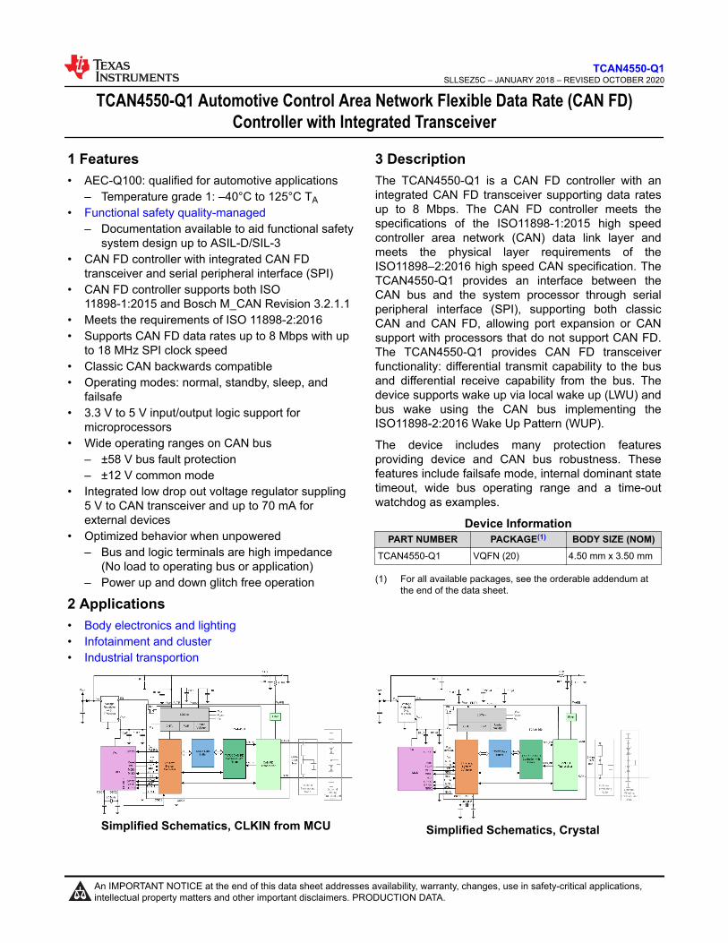
Simplified Schematics, CLKIN from MCU Simplified Schematics, Crystal
www.ti.comTCAN4550-Q1
SLLSEZ5C – JANUARY 2018 – REVISED OCTOBER 2020
Copyright © 2020 Texas Instruments Incorporated Submit Document Feedback 1
Product Folder Links: TCAN4550-Q1
TCAN4550-Q1SLLSEZ5C – JANUARY 2018 – REVISED OCTOBER 2020
An IMPORTANT NOTICE at the end of this data sheet addresses availability, warranty, changes, use in safety-critical applications,intellectual property matters and other important disclaimers. PRODUCTION DATA.
Table of Contents1 Features............................................................................12 Applications..................................................................... 13 Description.......................................................................14 Revision History.............................................................. 25 Pin Configuration and Functions...................................36 Specification.................................................................... 4
6.1 Absolute Maximum Ratings ....................................... 46.2 ESD Ratings .............................................................. 46.3 ESD Ratings, IEC ESD and ISO Transient
Specification ................................................................. 46.4 Recommended Operating Conditions ........................56.5 Thermal Information ...................................................56.6 Supply Characteristics ............................................... 66.7 Electrical Characteristics ............................................76.8 Timing Requirements ...............................................106.9 Switching Characteristics .........................................106.10 Typical Characteristics............................................ 12
7 Parameter Measurement Information.......................... 138 Detailed Description......................................................21
8.1 Overview................................................................... 218.2 Functional Block Diagram......................................... 22
8.3 Feature Description...................................................248.4 Device Functional Modes..........................................288.5 Programming............................................................ 418.6 Register Maps...........................................................45
9 Application and Implementation................................ 1299.1 Application Design Consideration........................... 1299.2 Typical Application.................................................. 133
10 Power Supply Recommendations............................13611 Layout.........................................................................137
11.1 Layout Guidelines................................................. 13711.2 Layout Example.................................................... 138
12 Device and Documentation Support........................13912.1 Documentation Support........................................ 13912.2 Receiving Notification of Documentation Updates13912.3 Support Resources............................................... 13912.4 Trademarks...........................................................13912.5 Electrostatic Discharge Caution............................13912.6 Glossary................................................................139
13 Mechanical, Packaging, and OrderableInformation.................................................................. 140
4 Revision HistoryNOTE: Page numbers for previous revisions may differ from page numbers in the current version.
Changes from Revision B (November 2019) to Revision C (October 2020) Page• Changed UVSUP rising max from 5.9 to 5.7 and added min value of 5.2...........................................................6• Added UVSUP falling max value of 5.0................................................................................................................ 6• Changed bit 2:0 To: 3:0 in Table 8-28 .............................................................................................................. 71
Changes from Revision A (April 2019) to Revision B (November 2019) Page• Added Functional safety quality-managed front page bullets............................................................................. 1• Changed VIO value IIL for SDI, SCK and nCS inputs in test conditions cell value from 0 V to 5.25 V................ 7• Changed Power Up Timing diagram VSUP ramp voltage level for INH turn on and timing..............................13• Added INH Brownout Behavior section in Application section........................................................................132
Changes from Revision * (October 2017) to Revision A (April 2019) Page• Changed the document status From: Advanced Information To: Production data ............................................ 1• Changed footnote Gauranteed to Specied throughout the electric table............................................................6• Added VIO values for tSOV.................................................................................................................................10• Changed Power Up Timing diagram VSUP ramp voltage level for INH turn on and timing. ............................13• Deleted CLKOUT from the GPIO1 circuit in Figure 8-2 ................................................................................... 22• Deleted CLKOUT: Off from Sleep Mode section in Figure 8-14 .......................................................................34• Deleted CLKOUT: Off From Sleep Mode section in Figure 8-15 ..................................................................... 34• Deleted bits 15 and 14 from GPO1_CONFIG from in Table 8-15 ....................................................................50• Changed CLKOUT_GPIO1_CONFIG To: GPIO1_CONFIG for GPO1_CONFIG in Table 8-15 ...................... 50• Changed the name of offset 1048 From: TDCE To: TDCR ..............................................................................61
TCAN4550-Q1SLLSEZ5C – JANUARY 2018 – REVISED OCTOBER 2020 www.ti.com
2 Submit Document Feedback Copyright © 2020 Texas Instruments Incorporated
Product Folder Links: TCAN4550-Q1
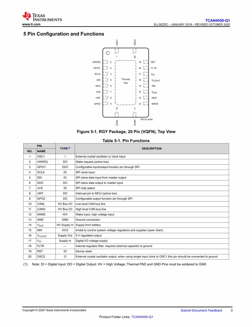
5 Pin Configuration and Functions
Thermal
Pad
2nWKRQ
3GPIO1
4SCLK
5SDI
6SDO
7nCS
8nINT
9GPO2
10
CA
NL
11
CA
NH
12 WAKE
13 GND
14 VSUP
15 INH
16 VCCOUT
17 VIO
18 FLTR
19 RST
20
OS
C2
1O
SC
1No t to scale
Figure 5-1. RGY Package, 20 Pin (VQFN), Top View
Table 5-1. Pin FunctionsPIN
TYPE(1) DESCRIPTIONNO. NAME
1 OSC1 I External crystal oscillator or clock input
2 nWKRQ DO Wake request (active low)
3 GPIO1 DI/O Configurable input/output function pin through SPI
4 SCLK DI SPI clock input
5 SDI DI SPI slave data input from master output
6 SDO DO SPI slave data output to master input
7 nCS DI SPI chip select
8 nINT DO Interrupt pin to MCU (active low)
9 GPO2 DO Configurable output function pin through SPI
10 CANL HV Bus I/O Low level CAN bus line
11 CANH HV Bus I/O High level CAN bus line
12 WAKE HVI Wake input, high voltage input
13 GND GND Ground connection
14 VSUP HV Supply In Supply from battery
15 INH HVO Inhibit to control system voltage regulators and supplies (open drain)
16 VCCOUT Supply Out 5 V regulated output
17 VIO Supply In Digital I/O voltage supply
18 FLTR — Internal regulator filter, requires external capacitor to ground
19 RST DI Device reset
20 OSC2 O External crystal oscillator output; when using single input clock to OSC1 this pin should be connected to ground
(1) Note: DI = Digital Input; DO = Digital Output; HV = High Voltage; Thermal PAD and GND Pins must be soldered to GND
www.ti.comTCAN4550-Q1
SLLSEZ5C – JANUARY 2018 – REVISED OCTOBER 2020
Copyright © 2020 Texas Instruments Incorporated Submit Document Feedback 3
Product Folder Links: TCAN4550-Q1

6 Specification
6.1 Absolute Maximum Ratingsover operating free-air temperature range for – 40 ≤ TA ≤ 125 (unless otherwise noted)(1)
MIN MAX UNITVSUP Supply voltage –0.3 42 V
VIO Supply voltage I/O level shifter –0.3 6 V
VCCOUT 5 V output supply –0.3 6 V
VBUS CAN bus I/O voltage (CANH, CANL) –58 58 V
VWAKE WAKE pin input voltage –0.3 42 V
VINH Inhibit pin output voltage –0.3 42 V
VLogic_Input Logic input terminal voltage –0.3 6 V
VSO Digital output terminal voltage –0.5 6 V
IO(SO) Digital output current 8 mA
IO(INH) Inhibit output current 4 mA
IO(WAKE) Wake current if due to ground shift V(WAKE) ≤ V(GND) – 0.3 V 3 mA
TJ Junction temperature –40 150 °C
Tstg Storage temperature –65 150 °C
(1) Stresses beyond those listed under Absolute Maximum Rating may cause permanent damage to the device. These are stress ratingsonly, which do not imply functional operation of the device at these or any other conditions beyond those indicated underRecommended Operating Condition. Exposure to absolute-maximum-rated conditions for extended periods may affect devicereliability.
6.2 ESD RatingsVALUE UNIT
V(ESD) Electrostatic dischargeHuman body model (HBM) classification level 3A per AEC Q100-002 Allterminal except for CANH and CANL. (1) WAKE terminals which are withrespect to ground only (2)
±4000 V
V(ESD) Electrostatic discharge Human body model (HBM) classification level H2 for CANH and CANL (2) ±15000 V
V(ESD) Electrostatic dischargeCharged device model (CDM)classification level C5, per AECQ100-011
All terminals ±750 V
(1) AEC Q100-002 indicates that HBM stressing shall be in accordance with the ANSI/ESDA/JEDEC JS-001 specification.(2) Terminals stressed with respect to GND
6.3 ESD Ratings, IEC ESD and ISO Transient SpecificationVALUE UNIT
V(ESD)Electrostatic discharge according to IBEE CANEMC (1)
Contact discharge ±8000 V
Air discharge ±15 000 V
V(ESD)Electrostatic discharge according toSAEJ2962-2 (2)
Contact discharge ±8000
V
Air discharge ±15 000
ISO7637 Transients according to IBEE CAN EMC test specCAN bus terminals (CANH and CANL), VSUP and WAKE (3)
Pulse 1 -100
Pulse 2 75
Pulse 3a -150
Pulse 3b 100
(1) IEC 61000-4-2 is a system-level ESD test. Results given here are specific to the IBEE LIN EMC Test specification conditions per IECTS 62228. Different system-level configurations may lead to different results
(2) SAEJ2962-2 Testing performed at 3rd party US3 approved EMC test facility, test report available upon request.
TCAN4550-Q1SLLSEZ5C – JANUARY 2018 – REVISED OCTOBER 2020 www.ti.com
4 Submit Document Feedback Copyright © 2020 Texas Instruments Incorporated
Product Folder Links: TCAN4550-Q1

(3) ISO7637 is a system-level transient test. Results given here are specific to the IBEE CAN EMC Test specification conditions. Differentsystem-level configurations may lead to different results.
6.4 Recommended Operating Conditionsover operating free-air temperature range for – 40 ≤ TA ≤ 125 (unless otherwise noted)
MIN TYP MAX UNITVSUP Supply voltage 5.5 30 V
VIO Logic pin supply voltage 3.135 5.25 V
IOH(DO) Digital terminal high-level output current –2 mA
IOL(DO) Digital terminal low-level output current 2 mA
IO (INH) INH output current 1 mA
C(FLTR) Filter pin capacitance See Power Supply Recommendations 300 nF
C(VCCOUT) VCCOUT supply capacitance See Power Supply Recommendations 10 µF
CWAKE External WAKE pin capacitance 10 nF
TSDR Thermal shutdown rising 160 TSDF Thermal shutdown falling 150 TSD(HYS) Thermal shutdown hysteresis 10
6.5 Thermal Information
THERMAL METRIC(1)
TCAN4550UNITPKG DES (RGY)
20 PINSRθJA Junction-to-ambient thermal resistance 35.2 °C/W
RθJC(top) Junction-to-case (top) thermal resistance 28.1 °C/W
RθJB Junction-to-board thermal resistance 12.8 °C/W
ΨJT Junction-to-top characterization parameter 0.3 °C/W
ΨJB Junction-to-board characterization parameter 12.7 °C/W
RθJC(bot) Junction-to-case (bottom) thermal resistance 1.1 °C/W
(1) For more information about traditional and new thermal metrics, see the Semiconductor and IC Package Thermal Metrics applicationreport.
www.ti.comTCAN4550-Q1
SLLSEZ5C – JANUARY 2018 – REVISED OCTOBER 2020
Copyright © 2020 Texas Instruments Incorporated Submit Document Feedback 5
Product Folder Links: TCAN4550-Q1

6.6 Supply Characteristicsover operating free-air temperature range for – 40 ≤ TA ≤ 125 (unless otherwise noted)
PARAMETER TEST CONDITIONS MIN TYP MAX UNIT
ISUP
Supply current, normal mode
Dominant
See Figure 7-3 RL = 60 Ω, CL =open. typical bus load. VCCOUT= no load
80 mA
See Figure 7-3 RL = 50 Ω, CL =open, high bus load. VCCOUT =no load
90 mA
Dominant with bus faultSee Figure 7-3 CANH = - 25 V,RL = open, CL = open VCCOUT =no load
180 mA
RecessiveSee Figure 7-3 RL = 60 Ω, CL =open, RCM = open, VCCOUT =no load
15 mA
Supply current, standby mode
See Figure 7-3 RL = 60 Ω, CL =open, -40°C < TA < 85°C,VCCOUT = no load, CANH/Lterminated to 2.5 V
3.5 mA
See Figure 7-3 RL = 60 Ω, CL =open, -40°C < TA < 85°C,VCCOUT = no load CANH/Lterminated to GND ± 100 mV
3.4 mA
ISUP Supply current, sleep mode SPI bus, OSC/CLKIN disabled:-40°C < TA < 85°C, VIO = 0 25 42 µA
IVIOI/O supply current normal modedominant I/O supply current
CLKIN = 40 MHz, VIO = 5 V 800 µA
Crystal = 40 MHz, VIO = 5 V 3 mA
IVIO I/O supply current, sleep mode I/O supply currentSleep Mode VIO = 5 V; OSC1 =CLKIN = 0 V and OSC2 = GND(2)
9 µA
IVCCOUT VCCOUT supply currentNormal Mode: VCCOUT = 5 V;-40°C < TA < 85°C SeeSection VCCOUT Pin
70 mA
UVSUP
Under voltage detection on VSUP rising ramp for protectedmode See Section Under Voltage
Lockout (UVLO) andUnpowered Device
5.2 5.5 5.7 V
Under voltage detection on VSUP falling ramp for protectedmode 4.5 4.7 5.0 V
UVIO
Under voltage detection on VIO rising ramp for protectedmode See Section Under Voltage
Lockout (UVLO) andUnpowered Device
2.45 2.6 V
Under voltage detection on VIO falling ramp for protectedmode 2.1 2.25 V
tUV/TSD Under voltage filter time and thermal shutdown timer (1)
Upon a UVIO event this timerstarts and provides time for VIOinput to return. See sectionThermal Shutdown fordescription of thermal shutdown.
200 500 ms
(1) Specified by design(2) When a crystal is used this current will be higher until the crystal's capacitors bleed off their energy. How much current and length of
time to bleed of the energy is system dependent and will not be specified.
TCAN4550-Q1SLLSEZ5C – JANUARY 2018 – REVISED OCTOBER 2020 www.ti.com
6 Submit Document Feedback Copyright © 2020 Texas Instruments Incorporated
Product Folder Links: TCAN4550-Q1
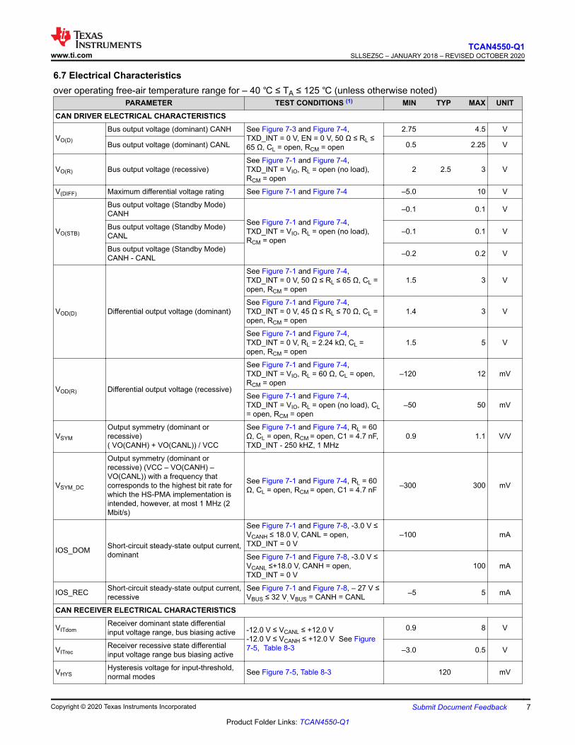
6.7 Electrical Characteristicsover operating free-air temperature range for – 40 ≤ TA ≤ 125 (unless otherwise noted)
PARAMETER TEST CONDITIONS (1) MIN TYP MAX UNITCAN DRIVER ELECTRICAL CHARACTERISTICS
VO(D)
Bus output voltage (dominant) CANH See Figure 7-3 and Figure 7-4,TXD_INT = 0 V, EN = 0 V, 50 Ω ≤ RL ≤65 Ω, CL = open, RCM = open
2.75 4.5 V
Bus output voltage (dominant) CANL 0.5 2.25 V
VO(R) Bus output voltage (recessive)See Figure 7-1 and Figure 7-4,TXD_INT = VIO, RL = open (no load),RCM = open
2 2.5 3 V
V(DIFF) Maximum differential voltage rating See Figure 7-1 and Figure 7-4 –5.0 10 V
VO(STB)
Bus output voltage (Standby Mode)CANH
See Figure 7-1 and Figure 7-4,TXD_INT = VIO, RL = open (no load),RCM = open
–0.1 0.1 V
Bus output voltage (Standby Mode)CANL –0.1 0.1 V
Bus output voltage (Standby Mode)CANH - CANL –0.2 0.2 V
VOD(D) Differential output voltage (dominant)
See Figure 7-1 and Figure 7-4,TXD_INT = 0 V, 50 Ω ≤ RL ≤ 65 Ω, CL =open, RCM = open
1.5 3 V
See Figure 7-1 and Figure 7-4,TXD_INT = 0 V, 45 Ω ≤ RL ≤ 70 Ω, CL =open, RCM = open
1.4 3 V
See Figure 7-1 and Figure 7-4,TXD_INT = 0 V, RL = 2.24 kΩ, CL =open, RCM = open
1.5 5 V
VOD(R) Differential output voltage (recessive)
See Figure 7-1 and Figure 7-4,TXD_INT = VIO, RL = 60 Ω, CL = open,RCM = open
–120 12 mV
See Figure 7-1 and Figure 7-4,TXD_INT = VIO, RL = open (no load), CL= open, RCM = open
–50 50 mV
VSYM
Output symmetry (dominant orrecessive)( VO(CANH) + VO(CANL)) / VCC
See Figure 7-1 and Figure 7-4, RL = 60Ω, CL = open, RCM = open, C1 = 4.7 nF,TXD_INT - 250 kHZ, 1 MHz
0.9 1.1 V/V
VSYM_DC
Output symmetry (dominant orrecessive) (VCC – VO(CANH) –VO(CANL)) with a frequency thatcorresponds to the highest bit rate forwhich the HS-PMA implementation isintended, however, at most 1 MHz (2Mbit/s)
See Figure 7-1 and Figure 7-4, RL = 60Ω, CL = open, RCM = open, C1 = 4.7 nF –300 300 mV
IOS_DOM Short-circuit steady-state output current,dominant
See Figure 7-1 and Figure 7-8, -3.0 V ≤VCANH ≤ 18.0 V, CANL = open,TXD_INT = 0 V
–100 mA
See Figure 7-1 and Figure 7-8, -3.0 V ≤VCANL ≤+18.0 V, CANH = open,TXD_INT = 0 V
100 mA
IOS_REC Short-circuit steady-state output current,recessive
See Figure 7-1 and Figure 7-8, – 27 V ≤VBUS ≤ 32 V, VBUS = CANH = CANL –5 5 mA
CAN RECEIVER ELECTRICAL CHARACTERISTICS
VITdomReceiver dominant state differentialinput voltage range, bus biasing active -12.0 V ≤ VCANL ≤ +12.0 V
-12.0 V ≤ VCANH ≤ +12.0 V See Figure7-5, Table 8-3
0.9 8 V
VITrecReceiver recessive state differentialinput voltage range bus biasing active –3.0 0.5 V
VHYSHysteresis voltage for input-threshold,normal modes See Figure 7-5, Table 8-3 120 mV
www.ti.comTCAN4550-Q1
SLLSEZ5C – JANUARY 2018 – REVISED OCTOBER 2020
Copyright © 2020 Texas Instruments Incorporated Submit Document Feedback 7
Product Folder Links: TCAN4550-Q1

6.7 Electrical Characteristics (continued)over operating free-air temperature range for – 40 ≤ TA ≤ 125 (unless otherwise noted)
PARAMETER TEST CONDITIONS (1) MIN TYP MAX UNIT
VIT(ENdom)
Receiver dominant state differentialinput voltage range, bus biasing inactive(VDiff)
-12.0 V ≤ VCANL ≤ +12.0 V-12.0 V ≤ VCANH ≤ +12.0 V See Figure7-5, Table 8-3
1.15 8 V
VIT(ENrec)
Receiver recessive state differentialinput voltage range, bus biasing inactive(VDiff)
-12.0 V ≤ VCANL ≤ +12.0 V-12.0 V ≤ VCANH ≤ +12.0 V See Figure7-5, Table 8-3
–3 0.4 V
VCM Common mode range: normal See Figure 7-5, Table 8-3 –12 12 V
VCM(EN) Common mode range: standby mode See Figure 7-5, Table 8-3 –12 12 V
IIOFF(LKG)Power-off (unpowered) bus inputleakage current
VCANH = VCANL = 5 V, Vsup to GND via 0Ω and 47 kΩ resistor 5 µA
CIInput capacitance to ground (CANH orCANL) 25 pF
CID Differential input capacitance 14 pF
RID Differential input resistanceTXD_INT = VCCINT, normal mode: -2.0 V≤ VCANH ≤+7.0 V; -2.0 V ≤VCANL ≤ + 7.0V
60 100 kΩ
RINSingle ended Input resistance (CANH orCANL)
-2.0 V ≤ VCANH ≤+7.0 V; -2.0 V ≤VCANL ≤+ 7.0 V 30 50 kΩ
RIN(M)Input resistance matching: [1 –(RIN(CANH) / (RIN(CANL))] × 100% VCANH = VCANL = 5.0 V –1 1 %
VCCOUT SUPPLY TERMINAL
VCCOUT 5 V output supply ICCOUT = -70 mA to 0 mA; VSUP = 5.5 Vto 18 V; -40°C < TA < 85°C 4.75 5 5.25 V
VDROP Drop out voltage VCCOUT = 5 V, VSUP = 12 V, ICCOUT = 70mA 300 500 mV
ΔVCC(ΔVSUP) Line regulation VSUP = 5.5 V to 30 V, ΔVCCOUT, ICCOUT= 10 mA 50 mV
ΔVCC(ΔVSUPL) Load regulation VSUP = 14 V, ICCOUT = 1 mA to 70mA, ΔVCCOUT, –40 ≤ TA ≤ 125 60 mV
UVCCOUT Under voltage threshold on VCCOUT 4.2 4.55 V
FLTR TERMINALVMEASURE Voltage measured at FLTR pin 1.5 V
C(FLTR) Filter pin capacitor External filter capacitor 300 330 nF
INH OUTPUT TERMINAL (HIGH VOLTAGE OUTPUT)
ΔVHHigh-level voltage drop INH with respectto VSUP
IINH = - 0.5 mA 0.5 1 V
ILKG(INH) Leakage current INH = 0 V, Sleep Mode –0.5 0.7 µA
WAKE INPUT TERMINAL (HIGH VOLTAGE INPUT)VIH High-level input voltage Standby mode, WAKE pin enabled VSUP–2 V
VIL Low-level input voltage Standby mode, WAKE pin enabled VSUP–3 V
IIH High-level input current WAKE = VSUP–1 V –25 –15 µA
IIL Low-level input current WAKE = 1 V 15 25 µA
tWAKE WAKE filter time Wake up filter time from a wake edge onWAKE; standby, sleep mode 50 µs
SDI, SCK, GPIO1 INPUT TERMINALSVIH High-level input voltage 0.7 VIO
VIL Low-level input voltage 0.3 VIO
IIH High-level input leakage current Inputs = VIO = 5.25 V –1 1 µA
IIL Low-level input leakage current Inputs = 0 V, VIO = 5.25 V –100 –5 µA
TCAN4550-Q1SLLSEZ5C – JANUARY 2018 – REVISED OCTOBER 2020 www.ti.com
8 Submit Document Feedback Copyright © 2020 Texas Instruments Incorporated
Product Folder Links: TCAN4550-Q1

6.7 Electrical Characteristics (continued)over operating free-air temperature range for – 40 ≤ TA ≤ 125 (unless otherwise noted)
PARAMETER TEST CONDITIONS (1) MIN TYP MAX UNITCIN Input capacitance 18 MHz 10 12 pF
ILKG(OFF)Unpowered leakage current (SDI andSCK only) Inputs = 5.25 V, VIO = VSUP = 0 V –1 1 µA
nCS INPUT TERMINALVIH High-level input voltage 0.7 VIO
VIL Low-level input voltage 0.3 VIO
IIH High-level input leakage current nCS = VIO = 5.25 V –1 1 µA
IIL Low-level input leakage current nCS = VIO = 5.25 V –50 –5 µA
ILKG(OFF) Unpowered leakage current nCS = 5.25 V, VIO = VSUP = 0 V –1 1 µA
RST INPUT TERMINALVIH High-level input voltage 0.7 VIO
VIL Low-level input voltage 0.3 VIO
IIH High-level input leakage current RST = VIO = 5.25 V 1 10 µA
IIL Low-level input leakage current RST = 0 V –1 1 µA
ILKG(OFF) Unpowered leakage current RST = VIO, VSUP = 0 V –7.5 7.5 µA
tPULSE_WIDTH Width of the input pulse 30 µs
SDO, GPIO1, GPO2 OUTPUT TERMINAL; nINT (OPEN DRAIIN) and nWKRQ (WHEN PROGRAMMED TO WORK OFF OF VIO AND ISOPEN DRAIN)VOH High-level output voltage 0.8 VIO
VOL Low-level output voltage 0.2 VIO
nWKRQ OUTPUT TERMINAL (DEFAULT INTERNAL VOLTAGE RAIL)
VOH High-level output voltage Default value when based upon internalvoltage rail 2.8 3.6 V
VOL Low-level output voltage Default value when based upon internalvoltage rail 0.7 V
OSC1 TERMINAL AND CRYSTAL SPECIFICATIONVIH High-level input voltage 0.85 1.10 VIO
VIL Low-level input voltage 0.3 VIO
FOSC1
Clock-In frequency tolerance , seesection Crystal and Clock InputRequirements
20 MHz –0.5 0.5 %
FOSC1
Clock-In frequency tolerance, seesection Crystal and Clock InputRequirements
40 MHz –0.5 0.5 %
tDC Input duty cycle 45 55 %
ESR Crystal ESR for load capacitance (2) 60 Ω
(1) All TXD_INT, RXD_INT and EN_INT references are for internal nodes that represent the same functions for a physical layertransceiver.
(2) Specified by design
www.ti.comTCAN4550-Q1
SLLSEZ5C – JANUARY 2018 – REVISED OCTOBER 2020
Copyright © 2020 Texas Instruments Incorporated Submit Document Feedback 9
Product Folder Links: TCAN4550-Q1

6.8 Timing Requirementsover operating free-air temperature range for – 40 ≤ TA ≤ 125 (unless otherwise noted)
MIN TYP MAX UNITMODE CHANGE TIMES (FULL DEVICE)
tMODE_STBY_NOMStandby to normal mode change time based upon SPIwrite 70 µs
tMODE_NOM_SLPSPI write to go to Sleep from Normal: INH and nWKRQturned off, See Figure 7-15 200 µs
tMODE_SLP_STBYWUP or LWU event until INH and nWKRQ asserted, SeeFigure 7-14 200 µs
tMODE_SLP_STBY_VCCOUT_ON WUP or LWU event until VCCOUT on, See Figure 7-14 1.5 ms
tMODE_NOM_STBYSPI write to go to standby from normal mode, See Figure7-16 200 µs
6.9 Switching Characteristicsover operating free-air temperature range for – 40 ≤ TA ≤ 125 (unless otherwise noted)
PARAMETER TEST CONDITIONS MIN TYP MAX UNITSWITCHING CHARACTERISTICS (CAN TRANSCEIVER ONLY)
tpHRPropagation delay time, high TXD_INTto Driver Recessive (1)
See Figure 7-4, RST = 0 V. Typicalconditions: RL = 60 Ω, CL = 100 pF, RCM= open
50 85 110 ns
tpLDPropagation delay time, low TXD_INT todriver dominant (1) 35 75 100 ns
tsk(p) Pulse skew (|tpHR – tpLD|) 30 40 ns
tR/F Differential output signal rise time: 8 55 75 ns
tpRHPropagation delay time, bus recessiveinput to high RXD_INT output See Figure 7-5, typical conditions:
CANL = 1.5 V, CANH = 3.5 V.
35 55 90 ns
tpDLPropagation delay time, bus dominantinput to RXD_INT low output 35 55 90 ns
DEVICE SWITCHING CHARACTERISTICS
tLOOP Loop delay(3)(CAN transceiver only)See Figure 7-6, RST = 0 V. typicalconditions: RL = 60 Ω, CL = 100 pF,CRXD = 15 pF
235 ns
tWK_FILTERBus time to meet filtered busrequirements for wake up request See Figure 8-6, standby mode. 0.5 1.8 µs
tWK_TIMEOUT
Bus wake-up timeout: time that a WUPmust take place within to be consideredvalid
See Figure 8-6 0.5 2.9 ms
tSILENCE Timeout for bus inactivity (6)Timer is reset and restarted when buschanges from dominant to recessive orvice versa.
0.6 1.2 s
tINACTIVE
Time required for the processor to clearwake flag or put the device into normalmode upon power up, power on reset orafter wake event otherwise the devicewill enter sleep mode (6)
2 4 6 min
tBiasTime from the start of a dominant-recessive-dominant sequence
Each phase 6 µs until Vsym ≥ 0.1.See Figure 7-10 250 µs
tPower_Up Power up time on VSUP (6) See Figure 7-13 250 µs
tTXD_INT_DTODominant time out(2) (CAN transceiveronly)(1) See Figure 8-7, RL = 60 Ω, CL = open 1 5 ms
TCAN4550-Q1SLLSEZ5C – JANUARY 2018 – REVISED OCTOBER 2020 www.ti.com
10 Submit Document Feedback Copyright © 2020 Texas Instruments Incorporated
Product Folder Links: TCAN4550-Q1

6.9 Switching Characteristics (continued)over operating free-air temperature range for – 40 ≤ TA ≤ 125 (unless otherwise noted)
PARAMETER TEST CONDITIONS MIN TYP MAX UNITTRANSMITTER AND RECEIVER SWITCHING CHARACTERISTICS
tBit(Bus)2MTransmitted recessive bit width @ 2Mbps See Figure 7-5, RST = 0 V typical
conditions: RL = 60 Ω, CL = 100 pF,CRXD = 15 pF
435 530 ns
tBit(Bus)5MTransmitted recessive bit width @ 5Mbps 155 210 ns
tBit(Bus)8M (5) Transmitted recessive bit width @ 8Mbps
See Figure 7-5, RST = 0 V typicalconditions: RL = 60 Ω, CL = 100 pF,CRXD = 15 pF
80 135 ns
tBit(RXD)2M Received recessive bit width @ 2 Mbps See Figure 7-5, RST = 0 V typicalconditions: RL = 60 Ω, CL = 100 pF,CRXD = 15 pF,
400 550 ns
tBit(RXD)5M Received recessive bit width @ 5 Mbps 120 220 ns
tBit(RXD)8M (5) Received recessive bit width @ 8 MbpsSee Figure 7-5, RST = 0 V typicalconditions: RL = 60 Ω, CL = 100 pF,CRXD = 15 pF
80 135 ns
ΔtRec (4)Receiver Timing symmetry @ 2 Mbps See Figure 7-5, RST = 0 V typical
conditions: RL = 60 Ω, CL = 100 pF,CRXD = 15 pF
–65 30 40 ns
Receiver Timing symmetry @ 5 Mbps –45 5 15 ns
SPI SWITCHING CHARACTERISTICSfSCK SCK, SPI clock frequency (6) 18 MHz
tSCK SCK, SPI clock period (6) See Figure 7-12 56 ns
tRSCK SCK rise time (6) See Figure 7-11 10 ns
tFSCK SCK fall time (6) See Figure 7-11 10 ns
tSCKH SCK, SPI clock high (6) See Figure 7-12 18 ns
tSCKL SCK, SPI clock low (6) See Figure 7-12 18 ns
tCSS Chip select setup time (6) See Figure 7-11 28 ns
tCSH Chip select hold time (6) See Figure 7-11 28 ns
tCSD Chip select disable time (6) See Figure 7-11 125 ns
tSISU Data in setup time (6) See Figure 7-11 5 ns
tSIH Data in hold time (6) See Figure 7-11 10 ns
tSOV Data out valid (6) VIO = 3.135 V to 5.25 V, See Figure7-12 20 ns
tRSO SO rise time (6) See Figure 7-12 10 ns
tFSO SO fall time (6) See Figure 7-12 10 ns
(1) All TXD_INT, RXD_INT, EN_INT and CAN transceiver only references are for internal nodes that represent the same functions for astand-alone transceiver.
(2) The TXD_INT dominant time out (tTXD_INT_DTO) disables the driver of the transceiver once the TXD_INT has been dominant longerthan tTXD_INT_DTO, which releases the bus lines to recessive, preventing a local failure from locking the bus dominant. The driver mayonly transmit dominant again after TXD_INT has been returned HIGH (recessive). While this protects the bus from local faults, lockingthe bus dominant, it limits the minimum data rate possible. The CAN protocol allows a maximum of eleven successive dominant bits(on TXD_INT) for the worst case, where five successive dominant bits are followed immediately by an error frame. This, along with thetTXD_INT_DTO minimum, limits the minimum bit rate. The minimum bit rate may be calculated by: Minimum Bit Rate = 11/ tTXD_INT_DTO =11 bits / 1.2 ms = 9.2 kbps.
(3) Time span from signal edge on TXD_INT input to next signal edge with same polarity on RXD output, the maximum of delay of bothsignal edges is to be considered.
(4) ΔtRec = tBit(RXD) – tBit(Bus)(5) Characterized but not 100% tested(6) Specified by design
www.ti.comTCAN4550-Q1
SLLSEZ5C – JANUARY 2018 – REVISED OCTOBER 2020
Copyright © 2020 Texas Instruments Incorporated Submit Document Feedback 11
Product Folder Links: TCAN4550-Q1

6.10 Typical Characteristics
VSUP (V)
I SU
P (P
A)
6 8 10 12 14 16 18 20 22 2420
22
24
26
28
30
32
34
36
38
D001
-40 °C25 °C55 °C85 °C100 °C125 °C
VCCOUT = 0 V ICCOUT = 0 mA CAN Bus Load = 60 Ω
Figure 6-1. ISUP vs VSUP Sleep Mode
VSUP (V)
I SU
P (
mA
)
6 8 10 12 14 16 18 20 22 2435
40
45
50
55
60
65
70
75
80
85
90
95
100
105
D003
-40 °C25 °C55 °C85 °C100 °C125 °C
VCCOUT = 5 V ICCOUT = 70 mA CAN Transceiver Off
Figure 6-2. ISUP Current Across Temperature andVSUP LDO Output Only.
TCAN4550-Q1SLLSEZ5C – JANUARY 2018 – REVISED OCTOBER 2020 www.ti.com
12 Submit Document Feedback Copyright © 2020 Texas Instruments Incorporated
Product Folder Links: TCAN4550-Q1
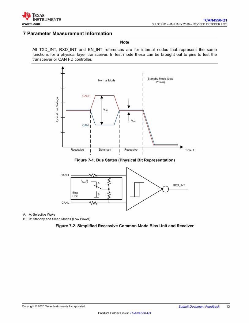
7 Parameter Measurement InformationNote
All TXD_INT, RXD_INT and EN_INT references are for internal nodes that represent the samefunctions for a physical layer transceiver. In test mode these can be brought out to pins to test thetransceiver or CAN FD controller.
Recessive Dominant Recessive Time, t
Typ
ica
l B
us V
olta
ge
Normal ModeStandby Mode (Low
Power)
CANL
CANH
Vdiff
Vdiff
Figure 7-1. Bus States (Physical Bit Representation)
Bias
Unit
RXD_INT
CANH
CANL
VCC/2A
B
A. A: Selective WakeB. B: Standby and Sleep Modes (Low Power)
Figure 7-2. Simplified Recessive Common Mode Bias Unit and Receiver
www.ti.comTCAN4550-Q1
SLLSEZ5C – JANUARY 2018 – REVISED OCTOBER 2020
Copyright © 2020 Texas Instruments Incorporated Submit Document Feedback 13
Product Folder Links: TCAN4550-Q1

RL
CANH
CANL
TXD_INT
CL
Figure 7-3. Supply Test Circuit
VODRL
CANH
CANL
TXD_INT
RCM
RCM
VCMCL
TXD_INT
0.9 V
0.5 V
VOD
tpLD tpHR
50% 50%
VO(CANH)
VO(CANL)
10%
tR tF
90%
0 V
VCC
Figure 7-4. Driver Test Circuit and Measurement
VOCL_RXD_INT
CANHRXD_INT
CANL
VID
VID
0.5 V
0.9 V
1.5 V
0 V
VO(RXD_INT)
70%
VOH
VOL
tpDL
tpRH
90%
10%
tR tF
IO
30%
Figure 7-5. Receiver Test Circuit and Measurement
TCAN4550-Q1SLLSEZ5C – JANUARY 2018 – REVISED OCTOBER 2020 www.ti.com
14 Submit Document Feedback Copyright © 2020 Texas Instruments Incorporated
Product Folder Links: TCAN4550-Q1
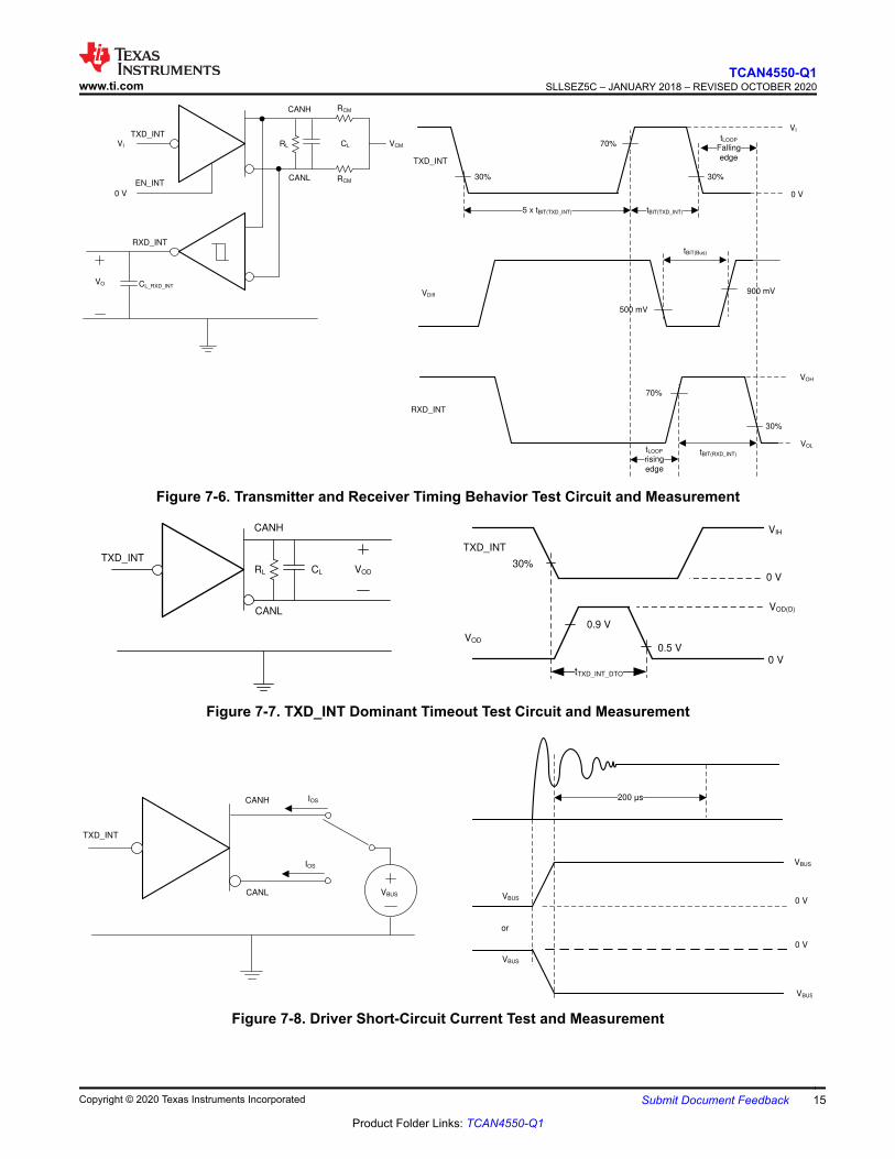
RL
CANH
CANL
TXD_INTCL
VO CL_RXD_INT
RXD_INT
EN_INT
VI
0 V
5 x tBIT(TXD_INT)
TXD_INT
RXD_INT
VOH
VOL
70%
70%
30%
tBIT(TXD_INT)
30%
tLOOP
Falling
edge
30%
VI
0 V
tBIT(RXD_INT)
RCM
RCM
VCM
VDiff
500 mV
900 mV
tBIT(Bus)
tLOOP
rising
edge
Figure 7-6. Transmitter and Receiver Timing Behavior Test Circuit and Measurement
VODRL
CANH
CANL
TXD_INTCL
TXD_INT
0.9 V
0.5 VVOD
0 V
VIH
tTXD_INT_DTO
0 V
VOD(D)
30%
Figure 7-7. TXD_INT Dominant Timeout Test Circuit and Measurement
CANH
CANL
TXD_INT
0 V
VBUS
VBUS
IOS
VBUS
0 V
VBUS
VBUS
or
200 s
IOS
Figure 7-8. Driver Short-Circuit Current Test and Measurement
www.ti.comTCAN4550-Q1
SLLSEZ5C – JANUARY 2018 – REVISED OCTOBER 2020
Copyright © 2020 Texas Instruments Incorporated Submit Document Feedback 15
Product Folder Links: TCAN4550-Q1

CVSUP
VSUP
VWAKE
INH
INH = H
VSUP
0 V
VSUP -1 V
tWAKE
VSUP - 2
TCAN4550
INH
VWAKE
VWAKE
INH
INH = H
VSUP
VSUP -1 V
tWAKE
VSUP - 3
OR
Figure 7-9. tWAKE While Monitoring INH Output
t > tWAKE_FILTER(MAX) t > tWAKE_FILTER(MAX) t > tWAKE_FILTER(MAX)
VDIFF
2.0 V
1.15 V
0.4 V
tBias
VSYM
0.1
Figure 7-10. Test Signal Definition for Bias Reaction Time Measurement
MSB In LSB
In
nCS
SCLK
SDI
SDO
tCSStRSCK tFSCK
tSISU tSIH
tCSH
tCSD
Figure 7-11. SPI AC Characteristic Write
TCAN4550-Q1SLLSEZ5C – JANUARY 2018 – REVISED OCTOBER 2020 www.ti.com
16 Submit Document Feedback Copyright © 2020 Texas Instruments Incorporated
Product Folder Links: TCAN4550-Q1
MSB OutLSB
Out
nCS
SCLK
SDI
SDO
tSCKH
tRSO tFSO
tSOV
tSCKL
tSCK
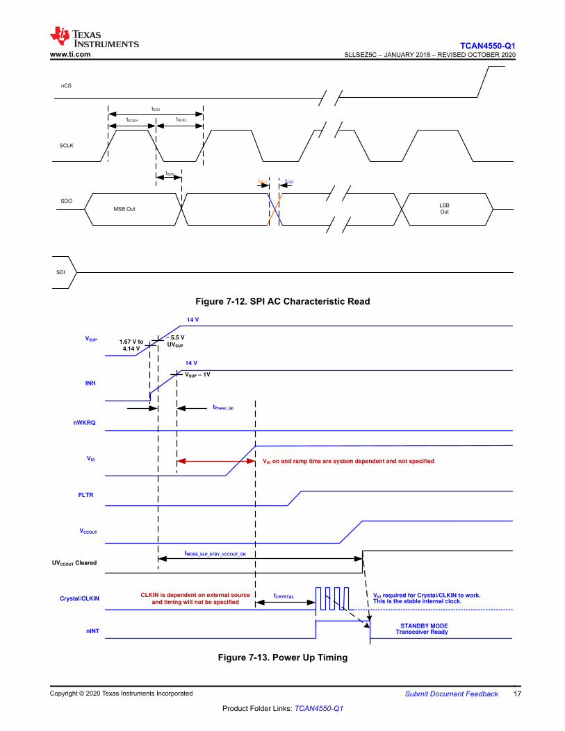
Figure 7-12. SPI AC Characteristic Read
VSUP
14 V
UVCCOUT Cleared
INH
FLTR
VCCOUT
VIO
Crystal/CLKIN
nINTSTANDBY MODE
Transceiver Ready
nWKRQ
VIO on and ramp time are system dependent and not specified
14 V
VIO required for Crystal/CLKIN to work. This is the stable internal clock.
VSUP ± 1V
1.67 V to
4.14 V
tPower_Up
CLKIN is dependent on external source
and timing will not be specifiedtCRYSTAL
tMODE_SLP_STBY_VCCOUT_ON
~ 5.5 V
UVSUP
Figure 7-13. Power Up Timing
www.ti.comTCAN4550-Q1
SLLSEZ5C – JANUARY 2018 – REVISED OCTOBER 2020
Copyright © 2020 Texas Instruments Incorporated Submit Document Feedback 17
Product Folder Links: TCAN4550-Q1

VSUP
14V
UVCCOUT Cleared
INH
FLTR
VCCOUT
VIO
Crystal/CLKIN
nINT STANDBY MODETransceiver Ready
nWKRQ
14V
VSUP ± 1V
Wake Event WUP or LWU
tMODE_SLP_STBY
tMODE_SLP_STBY_VCCOUT_ON
VIO on and ramp time are system dependent and not specified
VIO required for Crystal/CLKIN to work. This is the stable internal clock.
CLKIN is dependent on external source
and timing will not be specifiedtCRYSTAL
Figure 7-14. Sleep to Standby Timing
TCAN4550-Q1SLLSEZ5C – JANUARY 2018 – REVISED OCTOBER 2020 www.ti.com
18 Submit Document Feedback Copyright © 2020 Texas Instruments Incorporated
Product Folder Links: TCAN4550-Q1

VSUP
14V
EN_VCCOUT_S
INH
FLTR
VCCOUT
VIO
Crystal/CLKIN
Mode
120:6/3
Normal Mode
nWKRQ
14V
VSUP ± 1V
SPI Mode
Change
Normal to
Sleep CMD
tMODE_NOM_SLP
VIO off and ramp time are system dependent and not specified
VIO required for Crystal/CLKIN to work.
Sleep Mode
VCCOUT off ramp time is system dependent and not specified
tSILENCE Expires
Figure 7-15. Normal to Sleep Timing
www.ti.comTCAN4550-Q1
SLLSEZ5C – JANUARY 2018 – REVISED OCTOBER 2020
Copyright © 2020 Texas Instruments Incorporated Submit Document Feedback 19
Product Folder Links: TCAN4550-Q1

VSUP
14 V
INH
FLTR
VCCOUT
VIO
Crystal/CLKIN
Mode
120:6/3
Normal Mode
nWKRQ
14 V
SPI Mode
Change
Normal to
Standby CMD
tMODE_NOM_STBY
Standby Mode
Transceiver
5 V
High
Low
Figure 7-16. Normal to Standby Timing
TCAN4550-Q1SLLSEZ5C – JANUARY 2018 – REVISED OCTOBER 2020 www.ti.com
20 Submit Document Feedback Copyright © 2020 Texas Instruments Incorporated
Product Folder Links: TCAN4550-Q1

8 Detailed Description8.1 OverviewThe TCAN4550-Q1 is a CAN FD controller with an integrated CAN FD transceiver supporting data rates up to 8Mbps. The CAN FD controller meets the specifications of the ISO 11898-1:2015 high speed Controller AreaNetwork (CAN) data link layer and meets the physical layer requirements of the ISO 11898-2:2016 High SpeedController Area Network (CAN) specification providing an interface between the CAN bus and the CAN protocolcontroller supporting both classical CAN and CAN FD up to 5 megabits per second (Mbps). The TCAN4550-Q1provides CAN FD transceiver functionality: differential transmit capability to the bus and differential receivecapability from the bus. The device includes many protection features providing device and CAN bus robustness.The device can also wake up via remote wake up using CAN bus implementing the ISO 11898-2:2016 Wake UpPattern (WUP). Input/Output support for 3.3 V and 5 V microprocessors using VIO pin for seamless interface.The TCAN4550-Q1 has a Serial Peripheral Interface (SPI) that connects to a local microprocessor for thedevice's configuration; transmission and reception of CAN frames. The SPI interface supports clock rates up to18 MHz.
The CAN bus has two logical states during operation: recessive and dominant. See Figure 7-1 and Figure 7-2.
In the recessive bus state, the bus is biased to a common mode of 2.5 V via the high resistance internal inputresistors of the receiver of each node. Recessive is equivalent to logic high. The recessive state is also the idlestate.
In the dominant bus state, the bus is driven differentially by one or more drivers. Current flows through thetermination resistors and generates a differential voltage on the bus. Dominant is equivalent to logic low. Adominant state overwrites the recessive state.
During arbitration, multiple CAN nodes may transmit a dominant bit at the same time. In this case, the differentialvoltage of the bus is greater than the differential voltage of a single driver.
Transceivers with low power Standby Mode have a third bus state where the bus terminals are weakly biased toground via the high resistance internal resistors of the receiver. See Figure 7-1 and Figure 7-2. The TCAN4550-Q1 supports auto biasing, see Section 9.1.3.2
The TCAN4550-Q1 has the ability to configure many of the pins for multiple purposes and are described in moredetail in Section 8.3 section. Much of the parametric data is based on internal links like the TXD/RXD_INT whichrepresent the TXD and RXD of a standalone CAN transceiver. The TCAN4550-Q1 has a test mode that mapsthese signals to an external pin in order to perform compliance testing on the transceiver (TXD/RXD_INT_PHY)and CAN core (TXD/RXD_INT_CAN) independently.
www.ti.comTCAN4550-Q1
SLLSEZ5C – JANUARY 2018 – REVISED OCTOBER 2020
Copyright © 2020 Texas Instruments Incorporated Submit Document Feedback 21
Product Folder Links: TCAN4550-Q1

8.2 Functional Block Diagram
Note• OSC1 pin is either a crystal or external clock input• When OSC1 is used as an external clock input pin OSC2 must be connected directly to ground• When using an external clock input on OSC1 the input voltage should be the same as the VIO
voltage rail• The recommended crystal or clock rate to meet CAN FD 5 Mbps rates is 40 MHz
TCAN4550-Q1SLLSEZ5C – JANUARY 2018 – REVISED OCTOBER 2020 www.ti.com
22 Submit Document Feedback Copyright © 2020 Texas Instruments Incorporated
Product Folder Links: TCAN4550-Q1

VCCINT1
CANH
CANL
RXD_INT
Low Power Standby Bus
Receiver & Monitor
TXD_INT
EN_INT
DOMINANT
TIME OUT
OVER
TEMP
WAKE UP LOGIC /
MONITOR
M
U
X
LOGIC
OUTPUT
MODE AND CONTROL LOGIC
UNDER
VOLTAGE
BIA
S U
NIT
VLVRX
VSUP
WAKEWAKE
DRIVER
Transceiver Block Diagram
Communication Bus
TXD_INT_PHY
TXD_INT
RXD_INT
RXD_INT_PHY
WAKE
INH
INH_CNTL
VSUP
VSUP
Figure 8-1. CAN Transceiver Block Diagram
www.ti.comTCAN4550-Q1
SLLSEZ5C – JANUARY 2018 – REVISED OCTOBER 2020
Copyright © 2020 Texas Instruments Incorporated Submit Document Feedback 23
Product Folder Links: TCAN4550-Q1

SPI & I/O
Controller
SCLK
GPI01
SDI
SDO
nINT
RXD_INT_PHY
TXD_INT_CAN
SDO
SCLK
SDI
nCS
VIO
VIO
VIO
GPO
VIO
RST
VIO
VIO
VIO
GPI
Chip
Reset
nWKRQ
GPO2
VIO
VIO
3P6_SLEEP
EN_INT
Test Mode
WKRQ_VIO
WKRQ_3P6_SLEEP
Test Mode
RXD_INT_CAN
TXD_INT_PHYTest Mode
GPO2 ± for all non test mode
Figure 8-2. SPI and Digital IO Block Diagram
8.3 Feature Description8.3.1 VSUP Pin
This pin connects to the battery supply. It provides the supply to the internal regulators that support the digitalcore, CAN transceiver and VCCOUT . This Pin requires a 100 nF capacitor at the pin. See Section 10 for moreinformation. Upon power up; VSUP needs to rise above UVSUP rising threshold.
TCAN4550-Q1SLLSEZ5C – JANUARY 2018 – REVISED OCTOBER 2020 www.ti.com
24 Submit Document Feedback Copyright © 2020 Texas Instruments Incorporated
Product Folder Links: TCAN4550-Q1
8.3.2 VIO Pin
The VIO pin provides the digital IO voltage to match the microprocessor IO voltage thus avoiding therequirements for a level shifter. VIO supports IO pins SPI IO, GPIO1 and GPO2. It also provides power to theoscillator block supporting the crystal or CLKIN pins. It supports a range of 3.3 V to 5 V ± 5% nominal valueproviding the widest range of controller support. This pin requires a 100 nF capacitor at the pin. See Section 10for more information.
8.3.3 VCCOUT Pin
An internal LDO provides power for the integrated CAN transceiver and the VCCOUT pin for a total availablecurrent of 125 mA. The amount of current that can be sourced is dependent upon the CAN transceiverrequirements during normal operation. When a bus fault takes place that requires all the current from the LDO,the device is not able to source current to external components. During sleep mode this regulator is disabled andno current is provided. Once in the other active modes the regulator is enabled for normal operation. This pinrequires a 10 µF external capacitor as close to the pin as possible. See Section 10 for more information.
8.3.4 GND
This pin is a ground pin as is the thermal pad. Both need to connect to a ground plane to support heatdissipation.
8.3.5 INH Pin
The INH pin is a high voltage output pin that provides voltage from the VSUP minus a diode drop to enable anexternal high voltage regulator. These regulators are usually used to support the microprocessor and VIO pin.The INH function is on in all modes but sleep mode. In sleep mode the INH pin is turned off, going into a high Zstate. This allows the node to be placed into the lowest power state while in sleep mode. If this function is notrequired it can be disabled by setting register 16'h0800[9] = 1 using the SPI interface. If not required in the endapplication to initiate a system wake-up, INH can be left floating.
Note
This terminal should be considered a "high voltage logic" terminal. It is not a power output thus shouldbe used to drive the EN terminal of the system’s power management device. It should be not used asa switch for power management supply itself. This terminal is not reverse battery protected and thusshould not be connected outside of the system module.
8.3.6 WAKE Pin
The WAKE pin is used for a high voltage device local wake up (LWU). This function is explained further inSection 8.4.3.2 section. The pin is defaulted to bi-directional edge trigger, meaning it recognizes a LWU on eithera rising or falling edge of WAKE pin transition. This default value can be changed via a SPI command thatdisables the function, make it a rising edge only or a falling edge only. This is done by using register16'h0800[31:30]. Pin requires a 10 nF capacitor to ground for improved transient immunity in applications thatroute WAKE externally. If local wake-up functionality is not needed in the end application, WAKE can be tieddirectly to VSUP or GND.
8.3.7 FLTR Pin
This pin is used to provide filtering for the internal digital core regulator. Pin requires 300 nF of capacitance toground. See Section 10 for more information.
8.3.8 RST Pin
The RST pin is a device reset pin. It has a weak internal pull down resistor for normal operation. Ifcommunication has stopped with the TCAN4550-Q1, the RST pin can be pulsed high and then back low forgreater than tPULSE_WIDTH to perform a power on reset to the device. This resets the device to the default settingsand puts the device into standby mode. If the device was in normal or standby mode the INH and nWKRQ pinsremain active (on) and do not toggle; see Figure 8-3. If the device is in sleep mode and reset is toggled thedevice enters standby mode and at that time INH and nWKRQ turns on; see Figure 8-4.
www.ti.comTCAN4550-Q1
SLLSEZ5C – JANUARY 2018 – REVISED OCTOBER 2020
Copyright © 2020 Texas Instruments Incorporated Submit Document Feedback 25
Product Folder Links: TCAN4550-Q1

After a RST has taken place, a wait time of ≥ 700 µs should be used before reading or writing to the TCAN4550-Q1.
VSUP
14V
INH
VIO
nWKRQ
14V
Device SPI Access
Device ready to be read and written to
Standby Mode
RST
Low
High
tPULSE_WIDTH
700 µs
Normal or
Standby Mode
Figure 8-3. Timing for RST Pin in Normal and Standby Modes
VSUP
14V
INH
VIO
nWKRQ
Device SPI Access
Device ready to be read and written to
Standby Mode
RST
Float
High
tPULSE_WIDTH
700 µs
Sleep Mode
Low
14V
Low
250 µs
Figure 8-4. Timing for RST Pin in Sleep Mode
8.3.9 OSC1 and OSC2 Pins
These pins are used for a crystal oscillator. The OSC1 pin can also be used as a single-ended clock input fromthe microprocessor or some other clock source. See Section 9.1 section for further information on the functionsof these pins. It is recommended to provide a 40 MHz crystal or CLKIN to support CAN FD data rates.
8.3.10 nWKRQ Pin
This pin is a dedicated wake up request pin from a bus wake (WUP) request, local wake (LWU) request andpower on (PWRON). The nWKRQ pin is defaulted to a wake enable based upon a wake event. In thisconfiguration the output is pulled low and latched to serve as an enable for a regulator that does not use the INHpin to control voltage level. The nWKRQ pin can be configured by setting 16'h0800[8] = 1 as an interrupt pin thatpulls the output low, but once the wake interrupt flag is cleared it releases the output back to a high. This pin
TCAN4550-Q1SLLSEZ5C – JANUARY 2018 – REVISED OCTOBER 2020 www.ti.com
26 Submit Document Feedback Copyright © 2020 Texas Instruments Incorporated
Product Folder Links: TCAN4550-Q1
defaults to an internal 3.6 V rail that is active during sleep mode. In this configuration, if a wake event takesplace, the nWKRQ pin switches from high to low. This output can be configured to be powered from the VIO railthrough SPI programming, 16'h0800[19]. When powered off of the VIO pin, the device does not insert an interruptuntil the VIO rail is stable. When configured for VIO, this pin is an open drain output and requires an external pullup resistor to VIO rail. This configuration bit is saved for all modes of operation and does not reset in sleep mode.As some external regulators or power management chips may need a digital logic pin for a wake up request, thispin can be used.
Note• This pin is active low and is logical OR of CANINT, LWU and WKERR register 16'h0820 that are
not masked• If a pull-up resistor is placed on this pin it must be configured for power from the VIO rail
8.3.11 nINT Interrupt Pin
The nINT is a dedicated open drain global interrupt output pin. This pin needs an external pull-up resistor to VIOto function properly. All interrupt requests are reflected by this pin when pulled low.
In test mode, this pin is used as an EN pin input for testing the CAN transceiver and is shown as EN_INTthroughout the document. When this pin is high, the device is in normal mode and when low it is in standbymode. This is accomplished by writing 0 to register 16'h0800[0].
Note
This pin is an active low and is the logical OR of all faults in registers 16'h0820 and 16'h0824 that arenot masked.
8.3.12 GPIO1 Pin
This pin defaults out as the M_CAN_INT 1 (active low) interrupt. The functionality of the pin can be changed to aconfigurable output function pin by setting register 16'h0800[15:14] = 00. The GPO function is further configuredby using register 16'h0800[11:10]. To configure the pin to support a watchdog input timer reset pin use SPIregister 16'h0800[15:14] = 10.
When in test mode the GPIO1 pin is used to provide the input signal for the transceiver (TXD_INT_PHY) or theinput to the M_CAN core (RXD_INT_CAN). This is accomplished by first putting the device into test mode usingregister 16'h0800[21] = 1 and then selecting which part of the device is to be tested by setting register16'h0800[0]
www.ti.comTCAN4550-Q1
SLLSEZ5C – JANUARY 2018 – REVISED OCTOBER 2020
Copyright © 2020 Texas Instruments Incorporated Submit Document Feedback 27
Product Folder Links: TCAN4550-Q1

8.3.13 GPO2 Pin
The GPO2 pin is an open drain configurable output function pin that provides selected interrupts. This pin needsan external pull-up resistor to VIO to function properly. The output function can be changed by using register16'h0800[23:22] and can be configured as a watchdog output reset pin.
In test mode, this pin becomes the RXD_INT_PHY transceiver output or TXD_INT_CAN CAN Controller outputpin.
8.3.14 CANH and CANL Bus Pins
These are the CAN high and CAN low differential bus pins. These pins are connected to the CAN transceiverand the low voltage WUP CAN receiver. The functionality of these is explained throughout the document. Seesection Section 9.1.3.2 for can bus biasing.
8.4 Device Functional ModesThe TCAN4550-Q1 has several operating modes: normal, standby, and sleep modes and two protected modes.The first three mode selections are made by the SPI register. The two protected modes are modified standbymodes used to protect the device or bus. The TCAN4550-Q1 automatically goes from sleep to standby modewhen receiving a WUP or LWU event. See Table 8-1 for the various modes and what parts of the device areactive during the each mode.
The TCAN4550-Q1 state diagram figure, see Figure 8-5 , shows the biasing of the CAN bus in each of themodes of operation.
Table 8-1. Mode Overview
Mode RST Pin nINT nWKRQ INH GPO2Low
PowerCAN RX
WAKEPin WD SPI GPIO1 OSC CAN TX/
RX VCCOUT
Memory &Configuratio
n
Normal L On On On On Off Off On On On On On On Saved
Standby L On On On On On On On On On On Off On/ Saved
TSDProtected L On On On On On On On On On On Off Off Saved
UVIOProtected L Off On Off Off On On Off Off Off Off Mode
Dependent On Saved
Sleep L Off On Off Off On On Off Off Off Off Off Off Partial Saved
Note• In test mode the watchdog (WD) function can be used for Mode 01 CAN FD. The pin function for
WD is used by other pins in this mode but WD_ACTION reg16'h0800[17:16] = 00 and 01 areavailable and WD_BIT reg16'h0800[18] is how the timer would be reset.
TCAN4550-Q1SLLSEZ5C – JANUARY 2018 – REVISED OCTOBER 2020 www.ti.com
28 Submit Document Feedback Copyright © 2020 Texas Instruments Incorporated
Product Folder Links: TCAN4550-Q1

Normal Mode
RST: L
INH: H
Wake Pin: Active
All GPIO: Active
SPI: Active
OSC: Active
VCCOUT: Enabled
Power On
Start Up
Standby Mode
RST: L
Wake Sources: CAN, WAKE
INH: H
Wake Pin: Active
All GPIO: Active
SPI: Active
OSC: Active
VCCOUT: Enabled
Sleep Mode
RST: L
Wake Sources: CAN, WAKE
INH: floating
Wake Pin: Active
nINT Pin: Off
nWKRQ Pin: Active
Other GPIO: Off
SPI: Off
OSC: Off
VCCOUT: Off
SPI Write
MO = 00
SPI Write
MO = 01
SPI Write
MO = 10
NOTE: Upon a wake event the device will
transition into Standby mode and must be
reconfigured using SPI
Wake-up Event:
CAN bus
or
WAKE Pin
SPI Write
MO = 00
RST Pin: Set high to
reset device. Once
finished set back low
UVLO VSUP
TSD Protected
RST: L
Wake Sources: WAKE
INH: H
Wake Pin: Active
All GPIO: Active
SPI: Active
OSC: Active
VCCOUT: Off
Timer Start
Normal Mode
TSD = 1
TSD State
TSD Timer
TSD = 0 &
Timer Expires
TSD = 1 &
Timer Expires
UVIO Protected
RST: L
Wake Sources: CAN, WAKE
INH: H
Wake Pin: Active
All GPIO: Off
SPI: Off
OSC: Off
VCCOUT: On
Timer Start
UVIO State
UVIO Timer
UVIO = 1
UVIO = 1 Normal Mode
UVIO = 0
UVIO = 1 &
Timer Expires
TSD = 1
Resets Sleep
Core
Note:
x UVIO Protected status will lose the CLKIN/Crystal. During this time the digital core will reset and the M_CAN will have to be
reprogrammed. If timer times out and UVIO = 1 the device goes to sleep at which time all are cleared.
x If a Thermal Shutdown and UVIO event take place at the same time the device will enter sleep mode until the faults are rectified
Continued decrease below UVSUP
low the device will reset and clear
everything and come back on as if
a power up sequence has taken
place entering standby mode
Power Off
SWE timer
times out
Figure 8-5. Device State Diagram
8.4.1 Normal Mode
This is the normal operating mode of the device. The CAN driver and receiver are fully operational and CANcommunication is bi-directional. The driver translate a digital input on the internal TXD_INT signal from the CANFD controller to a differential output on CANH and CANL. The receiver translates the differential signal fromCANH and CANL to a digital output on the internal RXD_INT signal to the CAN FD controller. Normal mode isenabled or disabled via the SPI interface.
Note
If an under voltage event has taken place and cleared, the interrupt flags have to be cleared beforethe device can enter normal mode.
8.4.2 Standby Mode
In standby mode, the bus transmitter does not send data nor will the normal mode receiver accept data. Thereare several blocks that are active in this mode. The low power CAN receiver is active, monitoring the bus for thewake up pattern (WUP). The wake pin monitor is active. The SPI interface is active so that the microprocessorcan read and write registers in the memory for status and configuration. The INH pin is active in order to supplyan enable to the VIO controller if this function is used. The nWKRQ pin is low in this mode in the defaultconfiguration and can also be used as a digital enable pin to an external regulator or power managementintegrated circuit (PMIC). All other blocks are put into the lowest power state possible. This is the only mode thatthe TCAN4550-Q1 automatically switches to without a SPI transaction. The device goes from sleep mode tostandby mode automatically upon a bus WUP event or a local wake up from the wake pin. Upon entry to
www.ti.comTCAN4550-Q1
SLLSEZ5C – JANUARY 2018 – REVISED OCTOBER 2020
Copyright © 2020 Texas Instruments Incorporated Submit Document Feedback 29
Product Folder Links: TCAN4550-Q1

Standby Mode, only one wake interrupt is given (either LWU, CANINT ). New wake interrupts is not given instandby mode unless the device changes to normal or sleep mode and then back to standby. This prevents CANtraffic from spamming the processor with interrupts while in standby, and it gives the processor the first wakeinterrupt that was issued.
Upon power up, a power on reset or wake event from sleep mode the TCAN4550-Q1 enters standby mode. Thisstarts a four minute timer, tINACTIVE, that requires the processor to either reset the interrupt flags or configure thedevice to normal mode. This feature makes sure the node is in the lowest power mode if the processor does notcome up properly. This automatic mode change also takes place when the device has been put into sleep modeand receives a wake event, WUP or LWU. To disable this feature for sleep events register 16'h0800[1](SWE_DIS) must be set to one. This will not disable the feature when powering up or when a power on resettakes place.
8.4.3 Sleep Mode
Sleep mode is similar to the standby mode except the SPI interface and INH is disabled. As the low power CANreceiver is powered off of VSUP the implementer can turn off VIO. The nWKRQ pin is powered off the VSUP supplyinternal logic level regulator. This allows the TCAN4550-Q1 to provide an interrupt to the MCU when a wakeevent takes place with out requiring VIO to be up. When the device goes into sleep mode the power to theregisters and memory is removed to conserve power. This requires the device to be re-configured prior to beingput into normal mode. As the SPI interface is turned off the only ways to exit sleep mode is by a wake up event,RST pin toggle or power cycle. A sleep mode status flag is provided to determine if the device entered sleepmode through normal operation or if a fault caused the mode change. Register 16'h0820[23] provides the status.If a fault causes the device to enter sleep mode, this flag is set to a one.
Note
Difference between sleep and standby mode• Sleep mode reduces whole node power by shutting off INH/nWKRQ to MCU VREG and shuts off
SPI.• Standby mode reduces TCAN4550-Q1 power as INH and nWKRQ is enabled turning on node
MCU VREG and SPI interface is active.
Note
When entering sleep mode it is possible for the TCAN4550-Q1 to assert an interrupt due to UVCCOUTevent as the LDO is powering down. This interrupt should be ignored or can be masked out by using16'h830[22] before initiating the go to sleep command.
8.4.3.1 Bus Wake via RXD_INT Request (BWRR) in Sleep Mode
As the TCAN4550-Q1 supports low power sleep mode and uses a wake up from the CAN bus mechanism calledbus wake via RXD_INT Request (BWRR). Once this pattern is received, the TCAN4550-Q1 automaticallyswitches to standby mode and inserts an interrupt onto the nINT and nWKRQ pins to indicate to a hostmicroprocessor that the bus is active, and it should wake up and service the TCAN4550-Q1. The low powerreceiver and bus monitor are enabled in sleep mode to allow for RXD_INT Wake Requests via the CAN bus. Awake up request is output to the internal RXD_INT (driven low) as shown in Figure 8-7. The wake logic monitorsRXD_INT for transitions (high to low) and reactivate the device to standby mode based on the RXD_INT WakeRequest. The CAN bus terminals are weakly pulled to GND during this mode, see Figure 7-2.
These devices use the wake up pattern (WUP) from ISO 11898-2:2016 to qualify bus traffic into a request towake the host microprocessor. The bus wake request is signaled to the integrated CAN FD controller by a fallingedge and low corresponding to a “filtered” bus dominant on the RXD_INT terminal (BWRR).
The wake up pattern (WUP) consists of• A filtered dominant bus of at least tWK_FILTER followed by• A filtered recessive bus time of at least tWK_FILTER followed by• A second filtered dominant bus time of at least tWK_FILTER
TCAN4550-Q1SLLSEZ5C – JANUARY 2018 – REVISED OCTOBER 2020 www.ti.com
30 Submit Document Feedback Copyright © 2020 Texas Instruments Incorporated
Product Folder Links: TCAN4550-Q1

Once the WUP is detected, the device starts issuing wake up requests (BWRR) on the RXD_INT signal everytime a filtered dominant time is received from the bus. The first filtered dominant initiates the WUP and the busmonitor is now waiting on a filtered recessive, other bus traffic does not reset the bus monitor. Once a filteredrecessive is received, the bus monitor is now waiting on a filtered dominant and again, other bus traffic does notreset the bus monitor. Immediately upon receiving of the second filtered dominant the bus monitor recognizesthe WUP and transition to BWRR output. Immediately upon verification receiving a WUP the device transitionsthe bus monitor into BWRR mode, and indicates all filtered dominant bus times on the RXD_INT internal signalby driving it low for the dominant bus time that is in excess of tWK_FILTER, thus the RXD_INT output during BWRRmatches the classical 8 pin CAN devices that used the single filtered dominant on the bus as the wake uprequest mechanism from ISO 11898-2:2016.
For a dominant or recessive to be considered “filtered”, the bus must be in that state for more than tWK_FILTERtime. Due to variability in the tWK_FILTER the following scenarios are applicable.• Bus state times less than tWK_FILTER(MIN) are never detected as part of a WUP, and thus no BWRR is
generated.• Bus state times between tWK_FILTER(MIN) and tWK_FILTER(MAX) may be detected as part of a WUP and a BWRR
may be generated.• Bus state times more than tWK_FILTER(MAX) is always detected as part of a WUP, and thus, a BWRR is always
be generated.
See Figure 8-6 for the timing diagram of the WUP.
The pattern and tWK_FILTER time used for the WUP and BWRR prevents noise and bus stuck dominant faultsfrom causing false wake requests while allowing any CAN or CAN FD message to initiate a BWRR. If the deviceis switched to normal mode or an under voltage event occurs on VCC the BWRR is lost. The WUP pattern musttake place within the tWK_TIMEOUT time otherwise the device is in a state waiting for the next recessive and then avalid WUP pattern.
Bus VDiff
WWK_FILTER WWK_FILTER WWK_FILTER
Bus
Filtered
Dominant
Filtered
DominantFiltered
Recessive
Wake Up Pattern (WUP) ZKHUHWWWK_TIMEOUT
RXD_INT
WWK_FILTER
Filtered Dominant RXD Output
Bus Wake Via RXD Requests
Bus Wake via RXD
Request
Waiting for
Filtered Recessive
Waiting for
Filtered
Dominant
INH
nWKRQ
tMODE_SLP_STBY
Figure 8-6. Wake Up Pattern (WUP) and Bus Wake via RXD_INT Request (BWRR)
www.ti.comTCAN4550-Q1
SLLSEZ5C – JANUARY 2018 – REVISED OCTOBER 2020
Copyright © 2020 Texas Instruments Incorporated Submit Document Feedback 31
Product Folder Links: TCAN4550-Q1
Normal CAN communication
CAN Bus
Signal
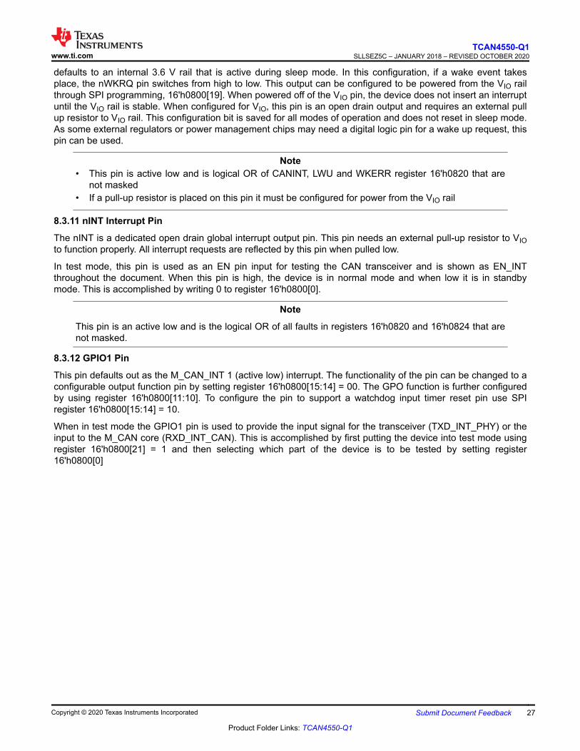
TXD fault stuck dominant: example PCB failure or bad software Fault is repaired & transmission capability
restored
TXD_INT (driver)
%XVZRXOGEH³VWXFNGRPLQDQW´EORFNLQJFRPPXQLFDWLRQIRUWKHZKROHQHWZRUNEXW7;''72
prevents this and frees the bus for communication after the time tTXD_DTO.
tTXD_DTO
Communication from local
node
Communication from repaired
node
RXD_INT
(receiver)
Communication from other
bus node(s)Communication from repaired
local node
Communication from other
bus node(s)
tTXD_DTO Driver disabled freeing bus for other nodes
Figure 8-7. Example timing diagram with TXD_INT DTO
8.4.3.2 Local Wake Up (LWU) via WAKE Input Terminal
The WAKE terminal is a high voltage input terminal which can be used for local wake up (LWU) request via avoltage transition. The terminal triggers a LWU event on either a low to high or high to low transition as it has bi-directional input thresholds. This terminal may be used with a switch to VSUP or ground. If the terminal is notused it should be pulled to ground or VSUP to avoid unwanted wake up events.
The LWU circuitry is active in sleep mode and standby mode. If a valid LWU event occurs, the device transitionsto standby mode. The LWU circuitry is not active in normal mode. To minimize system level current consumption,the internal bias voltages of the terminal follows the state on the terminal. The wake filter time for a valid wake toavoid glitches on wake pin is provided by filter value of tWAKE(MIN). A constant high level on WAKE has aninternal pull up to VSUP and a constant low level on WAKE has an internal pull down to GND. On power up, thismay look like a LWU event and could be flagged as such.
TCAN4550-Q1SLLSEZ5C – JANUARY 2018 – REVISED OCTOBER 2020 www.ti.com
32 Submit Document Feedback Copyright © 2020 Texas Instruments Incorporated
Product Folder Links: TCAN4550-Q1

RXD_INT
INH
WWWAKE
No Wake
UP
Wake
Wake
Threshold
Not Crossed
Mode Sleep Mode Standby Mode
Local Wake Request
WWWAKE
Wake UP
*
Figure 8-8. Local Wake Up – Rising Edge
INH
WWWAKE
No Wake
UP
Wake
Wake
Threshold
Not Crossed
Mode Sleep Mode Standby Mode
Local Wake Request
RXD_INT
WWWAKE
Wake UP
*
Figure 8-9. Local Wake Up – Falling Edge
Note
RXD_INT is an internal signal and can be seen in Transceiver test mode when VIO is present.
www.ti.comTCAN4550-Q1
SLLSEZ5C – JANUARY 2018 – REVISED OCTOBER 2020
Copyright © 2020 Texas Instruments Incorporated Submit Document Feedback 33
Product Folder Links: TCAN4550-Q1

8.4.4 Test Mode
The TCAN4550-Q1 includes a test mode that has four configurations. Two are enabled by the SPI interfaceusing the configuration register by setting register bit 16'h0800[21] = 1. In this mode the transceiverTXD_INT_PHY or CAN core RXD_INT_CAN can be mapped to the GPIO1 pin and RXD_INT_PHY orTXD_INT_CAN can be mapped to the GPO2 pin. EN_INT pin is mapped to the nINT pin, see Figure 8-10 andFigure 8-11 . This is accomplished by setting register 16'h0800[0] to 0 for transceiver testing or 1 for M_CANcore testing. This mapping is only valid when in test mode. There are two M_CAN core specific test modesentered using SPI but written to the M_CAN core registers directly, see Figure 8-12 and Figure 8-13.
SCLK
CANHVCCINT2
CANLSPI slave,
System Controller
SDI
SDO
nCS
nINT
GPIO1
GPO2
MCAN
Core
RX
TX
EN_INT
TXD_INT_PHY
RXD_INT_PHY
Figure 8-10. Transceiver Test Mode
SCLK
CANHVCCINT2
CANLSPI slave,
System
Controller
SDI
SDO
nCS
GPIO1
GPO2
MCAN
Core
RX
TX
RXD_INT_CAN
TXD_INT_CAN
Figure 8-11. SPI and M_CAN Core Test Mode
SCLK
CANHVCCINT2
CANLSPI slave,
System
Controller
SDI
SDO
nCS
MCAN
Core
RX
TX= 1
Figure 8-12. M_CAN Internal Loop Back Test Mode
SCLK
CANHVCCINT2
CANLSPI slave,
System Controller
SDI
SDO
nCS
MCAN
Core
RX
TX
Figure 8-13. M_CAN External Loop Back Test Mode
8.4.5 Failsafe Feature
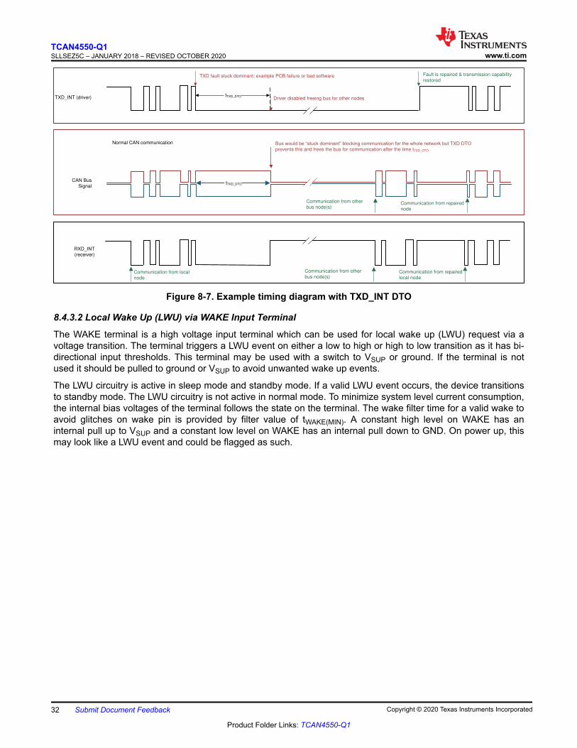
The TCAN4550-Q1 has three methods the failsafe feature is used in order to reduce node power consumptionfor a node system issue. Failsafe is the method the device uses to enter sleep mode from various other modes
TCAN4550-Q1SLLSEZ5C – JANUARY 2018 – REVISED OCTOBER 2020 www.ti.com
34 Submit Document Feedback Copyright © 2020 Texas Instruments Incorporated
Product Folder Links: TCAN4550-Q1
when specific issues arise. This feature uses the Sleep Wake Error (SWE) timer to determine if the nodeprocessor can communicate to the TCAN4550-Q1. The SWE timer is default enabled through the SWE_DIS;16'h0800[1] = 0 but can be disabled by writing a one to this bit. Even when the timer is disabled, a power onreset re-enables the timer and thus be active. Failsafe Feature is default disabled but can be enabled by writinga one to 16'h0800[13], FAILSAFE_EN.
Upon power up the SWE timer starts, tINACTIVE, the processor has typically four minutes to configure theTCAN4550-Q1, clear the PWRON flag or configure the device for normal mode; see Figure 8-14 . This featurecannot be disabled. If the device has not had the PWRON flag cleared or been placed into normal mode, itenters sleep mode. The device wakes up if the CAN bus provides a WUP or a local wake event takes place, thusentering standby mode. Once in standby mode tSILENCE and tINACTIVE timers starts. If tINACTIVE expires, thedevice re-enters sleep mode.
The second failure mechanism that causes the device to use the failsafe feature, if enabled, is when the devicereceives a CANINT, CAN bus wake (WUP) or WAKE pin (LWU), while in sleep mode such that the device leavessleep mode and enters standby mode. The processor has four minutes to clear the flags and place the deviceinto normal mode. If this does not happen the device enters sleep mode.
The third failure mechanism that causes the device to use the failsafe feature is when in standby or normal modeand the CANSLNT flag persists for tINACTIVE, the device enters sleep mode. Examples of events that couldcreate this are CLKIN or Crystal stops working, processor is no longer working and not able to exercise the SPIbus, a go-to-sleep command comes in and the processor is not able to receive it or is not able to respond. Seestate diagram Figure 8-15 .
Standby Mode
SWE Timer
tINACTIVE
Power On
Start Up
Sleep Mode
RST: L
Wake Sources: CAN, WAKE
INH: floating
Wake Pin: Active
nINT Pin: Off
nWKRQ Pin: Active
Other GPIO: Off
SPI: Off
OSC: Off
VCCOUT: Off
Stays in STBY mode
or switches to Normal mode if programmed
No &
Cleared
Timed out
Does timer
Expire and PWRON
flag cleared?
Figure 8-14. Power On Failsafe Feature
www.ti.comTCAN4550-Q1
SLLSEZ5C – JANUARY 2018 – REVISED OCTOBER 2020
Copyright © 2020 Texas Instruments Incorporated Submit Document Feedback 35
Product Folder Links: TCAN4550-Q1

SWE Timer
tINACTIVE
Normal Mode
0800[13] = 1
Fail Safe Mode En
Bus Inactivity
tSILENCE timerexpires
setting CANSLNT
flag
Sleep Mode
RST: L
Wake Sources: CAN, WAKE
INH: floating
Wake Pin: Active
nINT Pin: Off
nWKRQ Pin: Active
Other GPIO: Off
SPI: Off
OSC: Off
CLKOUT: Off
VCCOUT: Off
Does timer
expire?
No &
Cleared
SWE TimertINACTIVE
Monitoring CAN
Sleep Mode
RST: L
Wake Sources: CAN, WAKE
INH: floating
Wake Pin: Active
nINT Pin: Off
nWKRQ Pin: Active
Other GPIO: Off
SPI: Off
OSC: Off
VCCOUT: Off
Does timer
Expire and required
flags cleared?
Standby Mode
0800[13] = 1
Fail Safe Mode En
Bus Inactivity
Activity detected
leaving device in
current mode or
placing in selected
mode
Timed out
Figure 8-15. Normal and Standby Failsafe Feature
8.4.6 Protection Features
The TCAN4550-Q1 has several protection features that are described as follows.
8.4.6.1 Watchdog Function
The TCAN4550-Q1 contains a watchdog (WD) timeout function. When using the WD timeout function the WDruns continuously. The WD is default enabled and can be configured with four different timer values. WD isactive in normal and standby modes and off in sleep mode. Once the device enters standby or normal mode thetimer does not start until the first input trigger event. This event can be either writing a one to register16'h0800[18] or if selected, by changing the voltage level on the GPIO1 pin either high or low when configuredfor watchdog input. If the first trigger is not set the watchdog is disabled. The first trigger can happen in standbymode or normal mode. This is system implementation specific. While the timer is running, a SPI command
TCAN4550-Q1SLLSEZ5C – JANUARY 2018 – REVISED OCTOBER 2020 www.ti.com
36 Submit Document Feedback Copyright © 2020 Texas Instruments Incorporated
Product Folder Links: TCAN4550-Q1

writing a one to 16'h0800[18] resets the WD_TIMER timer or if configured for pin control the GPIO1 behaves asthe watchdog input bit.
The TCAN4550-Q1 has two ways of setting the trigger bit: via a SPI command and, if selected, through a GPI(GPIO1 configured as GPI). When a GPI pin is used any rising or falling edge resets the timer. A watchdog eventcan be conveyed back to the microprocessor in two methods: interrupt on nINT pin or, if selected, the GPO2 pincan be programmed to toggle upon a WD timeout. A timeout can initiate one of three actions by the TCAN4550-Q1: interrupt, INH toggle plus putting the device into standby mode or toggle watchdog output reset pin ifenabled. The input CLKIN or crystal values needs to be entered into reg 16'h0800[27] and is either 20 MHz or40MHz. See Table 8-2 for the register settings for the watchdog function.
Note
• If the device enters UVIO protected mode, the watchdog timer is held in reset. When the devicereturns to standby mode, the timer resumes counting.
• Once the command to enter sleep mode takes place, the WD timer is turned off and does nottrigger a watchdog event.
• If the any of the watchdog registers needs to be changed, the watchdog must be disabled and thechange made and then re-enabled.
Table 8-2. Watchdog Registers and DescriptionsAddress BIT(S) Field Type Reset DESCRIPTION
16'h0800
29:28 WD_TIMER R/W 2'b00
WD_TIMER: Watchdog timer
00 = 60 ms
01 = 600 ms
10 = 3 s
11 = 6 s
27 CLK_REF R/W 1'b1
CLK_REF: CLKIN/Crystal frequency reference
0 = 20 MHz
1 = 40 MHz
23:22 GPO2_CONFIG R/W 2'b00
GPO2_CONFIG: GPO2 configuration
00 = No action
01 = M_CAN_INT 0 interrupt (active low)
10 = Watchdog output
11 = Mirrors nINT pin
18 WD_BIT_SET W1C 1'b0
WD_BIT_SET: write a 1 to reset timer: if times out; this bit is set and thenthe selected action from register 16'h0800[17:16] takes place.
Note: This is a self-clearing bit. Writing a 1 resets the timer and then the bitclears.
17:16 WD_ACTION R/W 2'b00
WD_ACTION: Selected action when WD_TIMER times out
00 = Set interrupt flag and if a pin is configure to reflect WD output as aninterrupt the pin shows a low.
01 = Pulse INH pin and place device into standby mode – high - low - high≈300ms
10 = Pulse watchdog output pin if enabled – high - low - high ≈300ms
11 = Reserved
Note: Interrupt flag is always set for a WD timeout event.
www.ti.comTCAN4550-Q1
SLLSEZ5C – JANUARY 2018 – REVISED OCTOBER 2020
Copyright © 2020 Texas Instruments Incorporated Submit Document Feedback 37
Product Folder Links: TCAN4550-Q1
Table 8-2. Watchdog Registers and Descriptions (continued)Address BIT(S) Field Type Reset DESCRIPTION
16'h0800
15:14 GPIO1_CONFIG RW 2'b01
GPIO1_CONFIG: GPIO1 Pin Function Select
00 = GPO
01 = Reserved
10 = GPI – Automatically becomes a WD input trigger pin.
11 = Reserved
3 WD_EN RXU 1'b1
WD_EN - Watchdog Enable
0 = Disable
1 = Enabled
8.4.6.2 Driver and Receiver Function
The TXD_INT and RXD_INT are internal signal paths that behave like the TXD and RXD pins for a physical layertransceiver. During normal operation they are not accessible to external pins. The TCAN4550-Q1 provides a testmode that maps these signals to external pins see Section 8.4.4. The digital logic input and output levels forthese devices are CMOS levels with respect to VIO for compatibility with protocol controllers having 3.3 V to 5 Vlogic or I/O. Table 8-3 and Table 8-4 provides the states of the CAN driver and CAN receiver in each mode.
Table 8-3. Driver Function Table
DEVICE MODE TXD_INT INPUTBUS OUTPUTS
DRIVEN BUS STATECANH CANL
NormalL H L Dominant
H or Open Z Z Biased Recessive
Standby X Z Z Weak Pull to GND
Sleep X Z Z Weak Pull to GND
Table 8-4. Receiver Function Table Normal and Standby ModesDEVICE MODE CAN DIFFERENTIAL INPUTS
VID = VCANH – VCANLBUS STATE RXD_INT TERMINAL
Normal
VID ≥ 0.9 V Dominant L
0.5 V < VID < 0.9 V Undefined Undefined
VID ≤ 0.5 V Recessive H
Standby/Sleep
VID ≥ 1.15 V Dominant
See Figure 8-60.4 V < VID < 1.15 V Undefined
VID ≤ 0.4 V Recessive
Any Open (VID ≈ 0 V) Open H
8.4.6.3 Floating Terminals
There are internal pull ups and pull downs on critical terminals to place the device into known states if theterminal floats. See Table 8-5 for details on terminal bias conditions.
Table 8-5. Terminal BiasTERMINAL PULL UP or PULL DOWN COMMENT
SCLK Pull up Weakly biases input
SDI Pull up Weakly biases input
nCS Pull up Weakly biases input so the device is not selected
nWKRQ Pull up Weakly biases output when using internal voltage rail. When usingopen drain configuration an external pull up is be needed.
RST Pull down Weakly biases RST terminal towards normal operation mode
TCAN4550-Q1SLLSEZ5C – JANUARY 2018 – REVISED OCTOBER 2020 www.ti.com
38 Submit Document Feedback Copyright © 2020 Texas Instruments Incorporated
Product Folder Links: TCAN4550-Q1

Note
The internal bias should not be relied upon as only termination, especially in noisy environments butshould be considered a failsafe protection. Special care needs to be taken when the device is usedwith MCUs utilizing open drain outputs.
8.4.6.4 TXD_INT Dominant Timeout (DTO)
The TCAN4550-Q1 supports dominant state timeout. This is an internal function based upon the TXD_INT path.The transceiver can be tested for this by placing the device into test mode and putting a dominant on the GPIO1pin and monitor the GPO2 for RXD_INT_PHY. The TXD_INT DTO circuit prevents the local node from blockingnetwork communication in the event of a hardware or software failure where TXD_INT is held dominant (low)longer than the timeout period tTXD_INT_DTO. The TXD_INT DTO circuit is triggered by a falling edge on TXD_INT.If no rising edge is seen before the timeout constant of the circuit, tTXD_INT_DTO, the CAN driver is disabled. Thisfrees the bus for communication between other nodes on the network. The CAN driver is re-activated when arecessive signal (high) is seen on TXD_INT terminal, thus clearing the dominant timeout. The receiver remainsactive and the RXD_INT terminal reflects the activity on the CAN bus and the bus terminals is biased torecessive level during a TXD_INT DTO fault.
Note
The minimum dominant TXD_INT time allowed by the TXD_INT DTO circuit limits the minimumpossible transmitted data rate of the device. The CAN protocol allows a maximum of elevensuccessive dominant bits (on TXD_INT) for the worst case, where five successive dominant bits arefollowed immediately by an error frame.
8.4.6.5 CAN Bus Short Circuit Current Limiting
This device has several protection features that limit the short circuit current when a CAN bus line is shorted.These include CAN driver current limiting. The device has TXD_INT dominant timeout which preventspermanently having the higher short circuit current of dominant state in case of a system fault. During CANcommunication the bus switches between dominant and recessive states, thus the short circuit current may beviewed either as the current during each bus state or as a DC average current. For system current and powerconsiderations in the termination resistors and common mode choke ratings the average short circuit currentshould be used. The percentage dominant is limited by the TXD_INT dominant timeout and CAN protocol whichhas forced state changes and recessive bits such as bit stuffing, control fields, and inter frame space. Theseensure there is a minimum recessive amount of time on the bus even if the data field contains a high percentageof dominant bits.
Note
The short circuit current of the bus depends on the ratio of recessive to dominant bits and theirrespective short circuit currents. The average short circuit current may be calculated using Equation 1.
IOS(AVG) = %Transmit x [(%REC_Bits x IOS(SS)_REC) + (%DOM_Bits x IOS(SS)_DOM)] + [%Receive xIOS(SS)_REC]
(1)
Where• IOS(AVG) is the average short circuit current.• %Transmit is the percentage the node is transmitting CAN messages.• %Receive is the percentage the node is receiving CAN messages.• %REC_Bits is the percentage of recessive bits in the transmitted CAN messages.• %DOM_Bits is the percentage of dominant bits in the transmitted CAN messages.• IOS(SS)_REC is the recessive steady state short circuit current and IOS(SS)_DOM is the dominant steady
state short circuit current.
www.ti.comTCAN4550-Q1
SLLSEZ5C – JANUARY 2018 – REVISED OCTOBER 2020
Copyright © 2020 Texas Instruments Incorporated Submit Document Feedback 39
Product Folder Links: TCAN4550-Q1

Note
The short circuit current and possible fault cases of the network should be taken into considerationwhen sizing the power ratings of the termination resistance, other network components, and the powersupply used to generate VSUP.
8.4.6.6 Thermal Shutdown
This is a device preservation event. If the junction temperature of the device exceeds the thermal shut downthreshold, the device turns off the internal 5 V LDO for the CAN transceiver thus blocking the signal to bustransmission path as well as turning of the ability to source current and voltage to the VCCOUT pin. A thermal shutdown interrupt flag is set and an interrupt is inserted so that the microprocessor is informed. If this eventhappens, other interrupt flags may be set as an example a bus fault where the CAN bus is shorted to Vbat. Whenthis happens the digital core and SPI interface are still active. After a time of ≈ 300 ms the device checks thetemperature of the junction. The thermal shutdown (TSD) timer starts when TSD fault event starts and exits tostandby mode when a TSD fault is not present when the TSD timer is expired. While in thermal shut downprotected mode a SPI write to change the device to either Normal or Standby mode is ignored while writes tochange to sleep mode is accepted.
Note
If a thermal shut down event happens while the device is experiencing a VIO under voltage event thedevice enters sleep mode.
8.4.6.7 Under Voltage Lockout (UVLO) and Unpowered Device
The TCAN4550-Q1 monitors the VSUP , VIO and VCCOUT pin for undervoltage events. These voltage rails haveunder voltage detection circuitry which places the device into a protected state if an under voltage fault occursfor UVSUP and UVIO . This protects the bus during an under voltage event on these terminals. If VSUP is in undervoltage, the device loses the source needed to keep the internal regulators active. This causes the device to gointo a state where communication between the microprocessor and the TCAN4550-Q1 is disabled. TheTCAN4550-Q1 is not able to receive information from the bus, and thus does not pass any signals from the bus,including any Bus Wake via BWRR signals to the microprocessor. See Table 8-6 .
8.4.6.7.1 UVSUP and UVCCOUT
When VSUP drops to UVSUP level, the VCC CAN transceiver regulator loses the ability to maintain 5 V output. Atthis point, the UVCCOUT interrupt flag is set and the TCAN4550-Q1 turns off the regulator and place the CANtransceiver into a standby state. If VSUP returns to minimum levels the device enters standby mode. If VSUPcontinues to decrease to the power on reset level, the TCAN4550-Q1 shuts everything down. When VSUPreturns to acceptable levels the device will come up the same as initial power on. All registers are cleared andthe device has to be reconfigured.
8.4.6.7.2 UVIO
If VIO drops below UVIO under the voltage detection threshold, several functions are disabled. The transceiverswitchs off until VIO has recovered. The input clock or crystal circuits are disabled and the IO between theTCAN4550-Q1 and microprocessor is not active. When UVIO triggers the tUV timer starts. If the timer times outand the UVIO is still there, the device enters sleep mode, see Figure 8-5. Once in sleep mode a wake event isrequired to place the TCAN4550-Q1 into standby mode and enables the INH pin. As registers are cleared insleep mode the UVIO interrupt flag is lost. If the UVIO event is still in place, the cycle repeats. If during a thermalshut down event a UVIO event happens, the device automatically enters sleep mode.
The device is designed to be an "ideal passive" or “no load” to the CAN bus if the device is unpowered. The busterminals (CANH, CANL) have extremely low leakage currents when the device is unpowered so it does not loadthe bus. This is critical if some nodes of the network are unpowered while the rest of the of network remainsoperational. Logic terminals also have extremely low leakage currents when the device is unpowered, so they donot load other circuits which may remain powered.
The UVLO circuit monitors both rising and falling edge of a power rail when ramping and declining.
TCAN4550-Q1SLLSEZ5C – JANUARY 2018 – REVISED OCTOBER 2020 www.ti.com
40 Submit Document Feedback Copyright © 2020 Texas Instruments Incorporated
Product Folder Links: TCAN4550-Q1

Table 8-6. Under Voltage Lockout I and O Level Shifting DevicesVSUP VIO VCCOUT DEVICE STATE BUS RXD_INT
> UVSUP > UVVIO > UVCCOUT Normal Per TXD_INT Mirrors Bus
> UVSUP > UVVIO < UVCCOUT Protected High Impedance High (Recessive)
< UVSUP > UVVIO NA Protected High Impedance High (Recessive)
> UVSUP < UVVIO > UVCCOUT Protected Recessive High Impedance
< UVSUP < UVVIO NA Protected High Impedance High Impedance
Note
Once an under voltage condition and interrupt flags are cleared and the VSUP supply has returned tovalid level, the device typicallys need tMODE_CHANGE to transition to normal operation. The hostprocessor should not attempt to send or receive messages until this transition time has expired. If ENis low and VSUP has an under voltage event, the device goes into a protected mode which disables thewake up receiver and places the RXD_INT output into a high impedance state.
8.4.6.7.3 Fault and M_CAN Core Behavior:
During a UVIO, UVCCOUT or TSD fault the TCAN4550-Q1 automatically does the following to keep the M_CANcore in a known state. A write of 1 to CCCR.INIT will be issued anytime there is a transition from Normal →Standby. Any currently pending TX or RX processing is halted. Once the device re-enters Normal mode, a writeof 0 to CCCR.INIT is issued, and any pending messages (TXBRP active bits) is automatically transmitted.
8.4.7 CAN FD
The TCAN4550-Q1 performs CAN communication according to ISO 11898-1:2015 and Bosch CAN protocolspecification 3.2.1.1.
8.5 ProgrammingThe TCAN4550-Q1 uses 32 bit accesses. The TCAN4550-Q1 provides 2K bytes of MRAM that is fullyconfigurable for TX/RX buffer/FIFO as needed based upon the system needs. To avoid ECC errors right afterinitialization, the MRAM should be zeroed out during the initialization, power up, power on reset and wakeevents, a process thus ensuring ECC is properly calculated.
Note
At power up, MRAM values are unknown and thus ECC values is not valid. It is important that at least2 words (8 bytes) of payload data be written into any TX buffer element, even if the DLC is less than 8.Failure to do this results in a M_CAN BEU error, which puts the TCAN4550-Q1 device intoinitialization mode, and require user intervention before CAN communication can continue. One wayto avoid this, the MRAM should be zeroed out after power up, a power on reset or coming out of sleepmode.
8.5.1 SPI Communication
The SPI communication uses a standard SPI interface. Physically the digital interface pins are nCS (Chip SelectNot), SDI (Slave Data In), SDO (Slave Data Out) and SCLK (SPI Clock). Each SPI transaction is a 32 bit wordcontaining a command byte followed by two address bytes and length bytes. The data shifted out on the SDOpin for the transaction always starts with the Global Status Register (byte). This register provides the high levelstatus information about the device status. The two data bytes which are the ‘response’ to the command byte areshifted out next. Data bytes shifted out during a write command is content of the registers prior to the new databeing written and updating the registers. Data bytes shifted out during a read command are the current contentof the registers and the registers will not be updated.
The SPI input data on SDI is sampled on the low to high edge of the SCLK. The SPI output data on SDO ischanged on the high to low edge of the SCLK.
www.ti.comTCAN4550-Q1
SLLSEZ5C – JANUARY 2018 – REVISED OCTOBER 2020
Copyright © 2020 Texas Instruments Incorporated Submit Document Feedback 41
Product Folder Links: TCAN4550-Q1
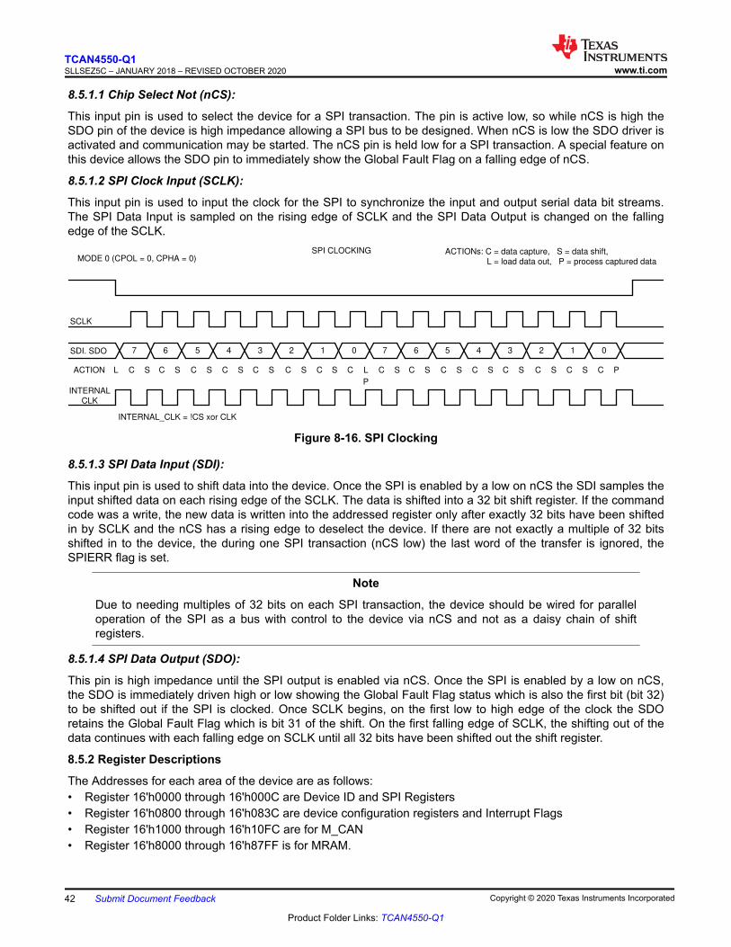
8.5.1.1 Chip Select Not (nCS):
This input pin is used to select the device for a SPI transaction. The pin is active low, so while nCS is high theSDO pin of the device is high impedance allowing a SPI bus to be designed. When nCS is low the SDO driver isactivated and communication may be started. The nCS pin is held low for a SPI transaction. A special feature onthis device allows the SDO pin to immediately show the Global Fault Flag on a falling edge of nCS.
8.5.1.2 SPI Clock Input (SCLK):
This input pin is used to input the clock for the SPI to synchronize the input and output serial data bit streams.The SPI Data Input is sampled on the rising edge of SCLK and the SPI Data Output is changed on the fallingedge of the SCLK.
SCLK
7
SPI CLOCKINGMODE 0 (CPOL = 0, CPHA = 0)
SDI. SDO 6 5 4 3 2 1 0 7 6 5 4 3 2 1 0
ACTION
ACTIONs: C = data capture, S = data shift,
L = load data out, P = process captured data
L C S C S C S C S C S C S C L
P
C S C S C S C S C S C S CS C S C P
INTERNAL
CLK
INTERNAL_CLK = !CS xor CLK
Figure 8-16. SPI Clocking
8.5.1.3 SPI Data Input (SDI):
This input pin is used to shift data into the device. Once the SPI is enabled by a low on nCS the SDI samples theinput shifted data on each rising edge of the SCLK. The data is shifted into a 32 bit shift register. If the commandcode was a write, the new data is written into the addressed register only after exactly 32 bits have been shiftedin by SCLK and the nCS has a rising edge to deselect the device. If there are not exactly a multiple of 32 bitsshifted in to the device, the during one SPI transaction (nCS low) the last word of the transfer is ignored, theSPIERR flag is set.
Note
Due to needing multiples of 32 bits on each SPI transaction, the device should be wired for paralleloperation of the SPI as a bus with control to the device via nCS and not as a daisy chain of shiftregisters.
8.5.1.4 SPI Data Output (SDO):
This pin is high impedance until the SPI output is enabled via nCS. Once the SPI is enabled by a low on nCS,the SDO is immediately driven high or low showing the Global Fault Flag status which is also the first bit (bit 32)to be shifted out if the SPI is clocked. Once SCLK begins, on the first low to high edge of the clock the SDOretains the Global Fault Flag which is bit 31 of the shift. On the first falling edge of SCLK, the shifting out of thedata continues with each falling edge on SCLK until all 32 bits have been shifted out the shift register.
8.5.2 Register Descriptions
The Addresses for each area of the device are as follows:• Register 16'h0000 through 16'h000C are Device ID and SPI Registers• Register 16'h0800 through 16'h083C are device configuration registers and Interrupt Flags• Register 16'h1000 through 16'h10FC are for M_CAN• Register 16'h8000 through 16'h87FF is for MRAM.
TCAN4550-Q1SLLSEZ5C – JANUARY 2018 – REVISED OCTOBER 2020 www.ti.com
42 Submit Document Feedback Copyright © 2020 Texas Instruments Incorporated
Product Folder Links: TCAN4550-Q1
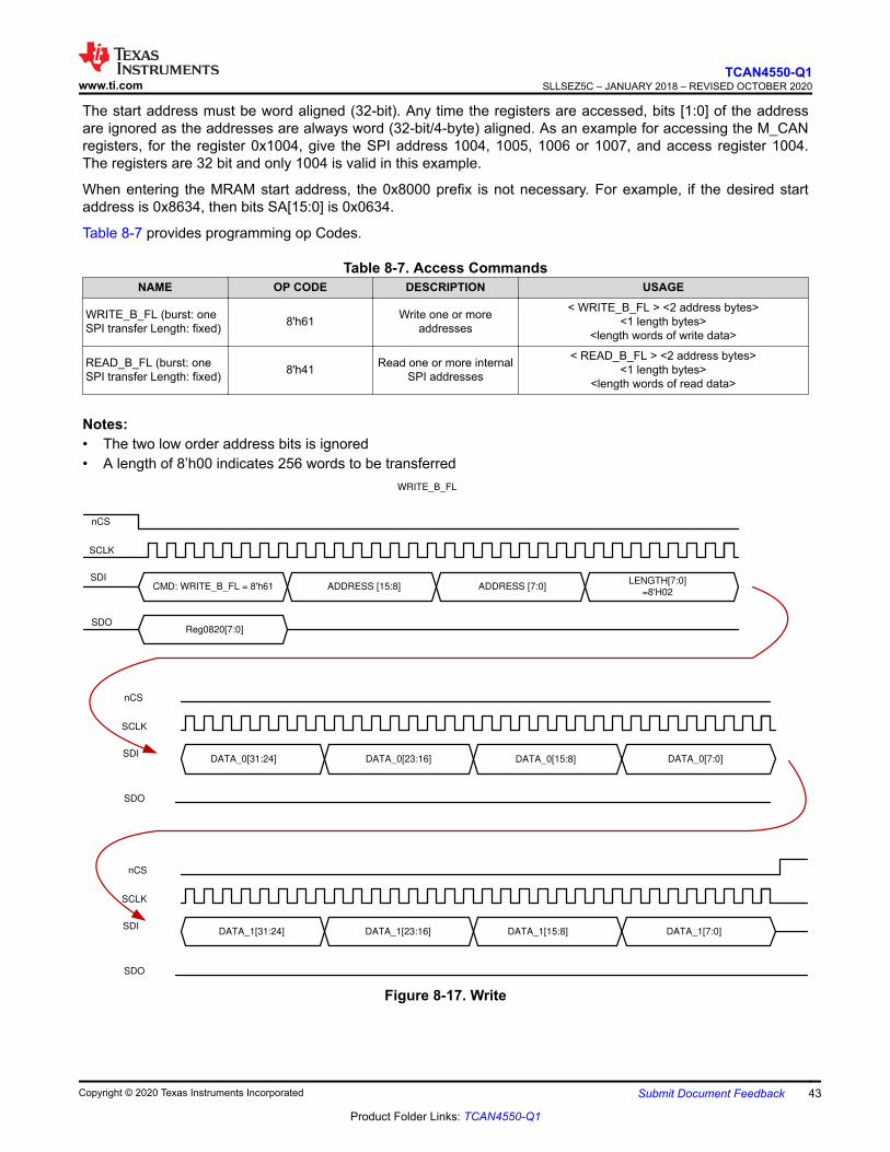
The start address must be word aligned (32-bit). Any time the registers are accessed, bits [1:0] of the addressare ignored as the addresses are always word (32-bit/4-byte) aligned. As an example for accessing the M_CANregisters, for the register 0x1004, give the SPI address 1004, 1005, 1006 or 1007, and access register 1004.The registers are 32 bit and only 1004 is valid in this example.
When entering the MRAM start address, the 0x8000 prefix is not necessary. For example, if the desired startaddress is 0x8634, then bits SA[15:0] is 0x0634.
Table 8-7 provides programming op Codes.
Table 8-7. Access CommandsNAME OP CODE DESCRIPTION USAGE
WRITE_B_FL (burst: oneSPI transfer Length: fixed) 8'h61 Write one or more
addresses
< WRITE_B_FL > <2 address bytes><1 length bytes>
<length words of write data>
READ_B_FL (burst: oneSPI transfer Length: fixed) 8'h41 Read one or more internal
SPI addresses
< READ_B_FL > <2 address bytes><1 length bytes>
<length words of read data>
Notes:• The two low order address bits is ignored• A length of 8’h00 indicates 256 words to be transferred
nCS
WRITE_B_FL
SDO
ADDRESS [15:8] ADDRESS [7:0]LENGTH[7:0]
=8'H02
DATA_0[31:24]
Reg0820[7:0]
SCLK
SDICMD: WRITE_B_FL = 8'h61
nCS
SDO
SCLK
SDI
nCS
SDO
SCLK
SDI
DATA_0[23:16] DATA_0[15:8] DATA_0[7:0]
DATA_1[31:24] DATA_1[23:16] DATA_1[15:8] DATA_1[7:0]
Figure 8-17. Write
www.ti.comTCAN4550-Q1
SLLSEZ5C – JANUARY 2018 – REVISED OCTOBER 2020
Copyright © 2020 Texas Instruments Incorporated Submit Document Feedback 43
Product Folder Links: TCAN4550-Q1

nCS
READ_B_FL
SDO
ADDRESS [15:8] ADDRESS [7:0]LENGTH[7:0]
=8'H02
DATA_0[31:24]
Reg0820[7:0]
SCLK
SDI CMD: READ_B_FL
= 8'h41
nCS
SDO
SCLK
SDI
nCS
SDO
SCLK
SDI
DATA_0[23:16] DATA_0[15:8] DATA_0[7:0]
DATA_1[31:24] DATA_1[23:16] DATA_1[15:8] DATA_1[7:0]
Figure 8-18. Read (Command OpCode 8h41)
TCAN4550-Q1SLLSEZ5C – JANUARY 2018 – REVISED OCTOBER 2020 www.ti.com
44 Submit Document Feedback Copyright © 2020 Texas Instruments Incorporated
Product Folder Links: TCAN4550-Q1

8.6 Register MapsThe TCAN4550-Q1 has a comprehensive register set with 32 bit addressing. The register is broken down intoseveral sections:• Section 8.6.1.• Section 8.6.2.• Section 8.6.3.• Section 8.6.4.
Note
All addresses are the lower order 16 address bit within the defined 32 bit address space.
Upper 16 address bits are ignored.
8.6.1 Device ID and Interrupt/Diagnostic Flag Registers: 16'h0000 to 16'h002F
This register block provided the device name and revision level. It provides all the interrupt flags as well.
Table 8-8. Device ID and Interrupt/Diagnostic Flag RegistersADDRESS REGISTER TCAN4550
VALUE ACCESS
‘h0000
DEVICE_ID[7:0] "T" 54 R
DEVICE_ID[15:8] "C" 43 R
DEVICE_ID[23:16] "A" 41 R
DEVICE_ID[31:24] "N" 4E R
‘h0004
DEVICE_ID[39:32] "4" 34 R
DEVICE_ID[47:40] "5" 35 R
DEVICE_ID[55:48] "5" 35 R
DEVICE_ID[63:56] "0" 30 R
‘h0008 SPI_2_revision, 8’h00 (Reserved), REV_ID Major, REV_ID Minor REV_IDMajor 00 R
‘h000C Status 00 R
Table 8-9. Device Configuration Access Type CodesAccess Type Code DescriptionRead Type
R R Read
Write Type
W W Write
WC W Write
Reset or Default Value
-n Value after reset or the default value
U U Undefined
www.ti.comTCAN4550-Q1
SLLSEZ5C – JANUARY 2018 – REVISED OCTOBER 2020
Copyright © 2020 Texas Instruments Incorporated Submit Document Feedback 45
Product Folder Links: TCAN4550-Q1
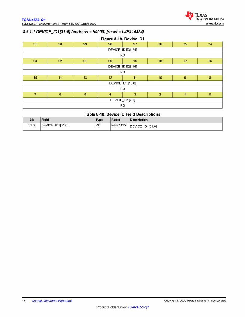
8.6.1.1 DEVICE_ID1[31:0] (address = h0000) [reset = h4E414354]
Figure 8-19. Device ID131 30 29 28 27 26 25 24
DEVICE_ID1[31:24]
RO
23 22 21 20 19 18 17 16
DEVICE_ID1[23:16]
RO
15 14 13 12 11 10 9 8
DEVICE_ID1[15:8]
RO
7 6 5 4 3 2 1 0
DEVICE_ID1[7:0]
RO
Table 8-10. Device ID Field DescriptionsBit Field Type Reset Description
31:0 DEVICE_ID1[31:0] RO h4E414354 DEVICE_ID1[31:0]
TCAN4550-Q1SLLSEZ5C – JANUARY 2018 – REVISED OCTOBER 2020 www.ti.com
46 Submit Document Feedback Copyright © 2020 Texas Instruments Incorporated
Product Folder Links: TCAN4550-Q1

8.6.1.2 DEVICE_ID2[31:0] (address = h0004) [reset = h30353534]
Figure 8-20. Device ID231 30 29 28 27 26 25 24
DEVICE_ID2[31:24]
RO
23 22 21 20 19 18 17 16
DEVICE_ID2[23:16]
RO
15 14 13 12 11 10 9 8
DEVICE_ID2[15:8]
RO
7 6 5 4 3 2 1 0
DEVICE_ID2[7:0]
RO
Table 8-11. Device ID Field DescriptionsBit Field Type Reset Description
31:0 DEVICE_ID2[31:0] RO h30353534 DEVICE_ID2[63:32]
www.ti.comTCAN4550-Q1
SLLSEZ5C – JANUARY 2018 – REVISED OCTOBER 2020
Copyright © 2020 Texas Instruments Incorporated Submit Document Feedback 47
Product Folder Links: TCAN4550-Q1
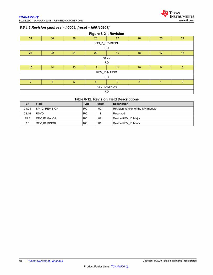
8.6.1.3 Revision (address = h0008) [reset = h00110201]
Figure 8-21. Revision31 30 29 28 27 26 25 24
SPI_2_REVISION
RO
23 22 21 20 19 18 17 16
RSVD
RO
15 14 13 12 11 10 9 8
REV_ID MAJOR
RO
7 6 5 4 3 2 1 0
REV_ID MINOR
RO
Table 8-12. Revision Field DescriptionsBit Field Type Reset Description
31:24 SPI_2_REVISION RO h00 Revision version of the SPI module
23:16 RSVD RO h11 Reserved
15:8 REV_ID MAJOR RO h02 Device REV_ID Major
7:0 REV_ID MINOR RO h01 Device REV_ID Minor
TCAN4550-Q1SLLSEZ5C – JANUARY 2018 – REVISED OCTOBER 2020 www.ti.com
48 Submit Document Feedback Copyright © 2020 Texas Instruments Incorporated
Product Folder Links: TCAN4550-Q1
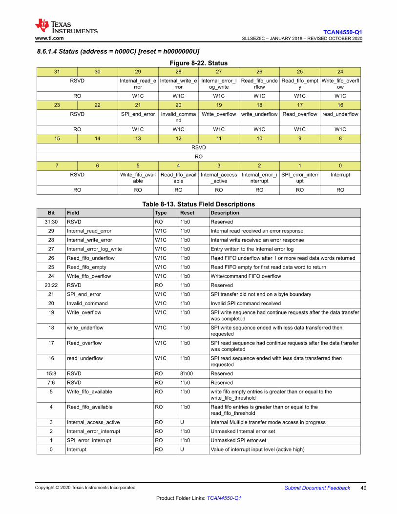
8.6.1.4 Status (address = h000C) [reset = h0000000U]
Figure 8-22. Status31 30 29 28 27 26 25 24
RSVD Internal_read_error
Internal_write_error
Internal_error_log_write
Read_fifo_underflow
Read_fifo_empty
Write_fifo_overflow
RO W1C W1C W1C W1C W1C W1C
23 22 21 20 19 18 17 16
RSVD SPI_end_error Invalid_command
Write_overflow write_underflow Read_overflow read_underflow
RO W1C W1C W1C W1C W1C W1C
15 14 13 12 11 10 9 8
RSVD
RO
7 6 5 4 3 2 1 0
RSVD Write_fifo_available
Read_fifo_available
Internal_access_active
Internal_error_interrupt
SPI_error_interrupt
Interrupt
RO RO RO RO RO RO RO
Table 8-13. Status Field DescriptionsBit Field Type Reset Description
31:30 RSVD RO 1’b0 Reserved
29 Internal_read_error W1C 1’b0 Internal read received an error response
28 Internal_write_error W1C 1’b0 Internal write received an error response
27 Internal_error_log_write W1C 1’b0 Entry written to the Internal error log
26 Read_fifo_underflow W1C 1’b0 Read FIFO underflow after 1 or more read data words returned
25 Read_fifo_empty W1C 1’b0 Read FIFO empty for first read data word to return
24 Write_fifo_overflow W1C 1’b0 Write/command FIFO overflow
23:22 RSVD RO 1’b0 Reserved
21 SPI_end_error W1C 1’b0 SPI transfer did not end on a byte boundary
20 Invalid_command W1C 1’b0 Invalid SPI command received
19 Write_overflow W1C 1’b0 SPI write sequence had continue requests after the data transferwas completed
18 write_underflow W1C 1’b0 SPI write sequence ended with less data transferred thenrequested
17 Read_overflow W1C 1’b0 SPI read sequence had continue requests after the data transferwas completed
16 read_underflow W1C 1’b0 SPI read sequence ended with less data transferred thenrequested
15:8 RSVD RO 8’h00 Reserved
7:6 RSVD RO 1’b0 Reserved
5 Write_fifo_available RO 1’b0 write fifo empty entries is greater than or equal to thewrite_fifo_threshold
4 Read_fifo_available RO 1’b0 Read fifo entries is greater than or equal to theread_fifo_threshold
3 Internal_access_active RO U Internal Multiple transfer mode access in progress
2 Internal_error_interrupt RO 1’b0 Unmasked Internal error set
1 SPI_error_interrupt RO 1’b0 Unmasked SPI error set
0 Interrupt RO U Value of interrupt input level (active high)
www.ti.comTCAN4550-Q1
SLLSEZ5C – JANUARY 2018 – REVISED OCTOBER 2020
Copyright © 2020 Texas Instruments Incorporated Submit Document Feedback 49
Product Folder Links: TCAN4550-Q1

8.6.2 Device Configuration Registers: 16'h0800 to 16'h08FF
Registers not listed are reserved and return h’00.
Table 8-14. Device Configuration RegistersADDRESS REGISTER VALUE ACCESS
0800 Modes of Operation and Pin Configurations h'C8000468 R/W/U
0804 Timestamp Prescalar h’00000002 R/W
0808 Read and Write Test Registers h’00000000 R/W
080C – 0810 ECC and TDR Registers h'00000000 R/W/U
0814 -081C Reserved h'00000000 R
0820 Interrupt Flags h'00000000 R
0824 MCAN Interrupt Flags h’00000000 R
0829 – 082F Reserved h'00000000 R
0830 Interrupt Enable h’FFFFFFFF R/W
0834 – 083F Reserved h'00000000 R
Note
The following bits are being saved when entering sleep mode and will show up bold in register maps.• 16'h0800 bits 0, 1, 8, 9, 10, 11, 13, 14, 15, 19, 21, 22, 23, 30 and 31.• 16'h0820 bits 18, 19 and 21• 16'h0830 bits 14 and 15
8.6.2.1 Modes of Operation and Pin Configuration Registers (address = h0800) [reset = hC8000468]
Figure 8-23. Modes of Operation and Pin Configuration Registers31 30 29 28 27 26 25 24
WAKE_CONFIG WD_TIMER CLK_REF RSVD RSVD RSVD
R/W R/W R/W R R R
23 22 21 20 19 18 17 16
GPO2_CONFIG TEST_MODE_EN
RSVD nWKRQ_VOLTAGE
WD_BIT_SET WD_ACTION
R/W R/W R R/W R/W R/W
15 14 13 12 11 10 9 8GPIO1_CONFIG FAIL_SAFE_E
NRSVD GPIO1_GPO_CONFIG INH_DIS nWKRQ_CONF
IGR/W R/W R R/W R/W R/W
7 6 5 4 3 2 1 0MODE_SEL RSVD RSVD WD_EN DEVICE_RESE
TSWE_DIS TEST_MODE_
CONFIGR/W/U R R R/W/U R/W/U R/W R/W
Table 8-15. Modes of Operation and Pin Configuration Registers Field DescriptionsBit Field Type Reset Description
31:30 WAKE_CONFIG R/W 2’b11
WAKE_CONFIG: Wake pin configuration00 = Disabled01 = Rising edge10 = Falling edge11 = Bi-Directional – either edge
TCAN4550-Q1SLLSEZ5C – JANUARY 2018 – REVISED OCTOBER 2020 www.ti.com
50 Submit Document Feedback Copyright © 2020 Texas Instruments Incorporated
Product Folder Links: TCAN4550-Q1
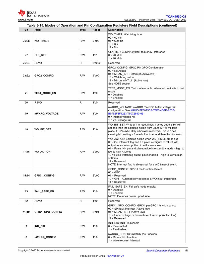
Table 8-15. Modes of Operation and Pin Configuration Registers Field Descriptions (continued)Bit Field Type Reset Description
29:28 WD_TIMER R/W 2’b00
WD_TIMER: Watchdog timer00 = 60 ms01 = 600 ms10 = 3 s11 = 6 s
27 CLK_REF R/W 1'b1CLK_REF: CLKIN/Crystal Frequency Reference0 = 20 MHz1 = 40 MHz
26:24 RSVD R 3'b000 Reserved
23:22 GPO2_CONFIG R/W 2’b00
GPO2_CONFIG: GPO2 Pin GPO Configuration00 = No Action01 = MCAN_INT 0 interrupt (Active low)10 = Watchdog output11 = Mirrors nINT pin (Active low)See NOTE section
21 TEST_MODE_EN R/W 1'b0
TEST_MODE_EN: Test mode enable. When set device is in testmode0 = Disabled1 = Enabled
20 RSVD R 1'b0 Reserved
19 nWKRQ_VOLTAGE R/W 1’b0
nWKRQ_VOLTAGE: nWKRQ Pin GPO buffer voltage railconfiguration: See #GUID-7F8075CA-78F3-4D7E-A637-B9752F8F1263/T5072690-660 = Internal voltage rail1 = VIO voltage rail
18 WD_BIT_SET R/W 1’b0
WD_BIT_SET: Write a 1 to reset timer: if times out this bit willset and then the selected action from 0800[17:16] will takeplace. (TCAN4x50 Only otherwise reserved) This is a self-clearing bit. Writing a 1 resets the timer and then the bit clears
17:16 WD_ACTION R/W 2’b00
WD_ACTION: Selected action when WD_TIMER times out00 = Set interrupt flag and if a pin is configure to reflect WDoutput as an interrupt the pin will show a low.01 = Pulse INH pin and placedevice into standby mode – high tolow to high ≈300ms10 = Pulse watchdog output pin if enabled – high to low to high≈300ms11 = ReservedNOTE: Interrupt flag is always set for a WD timeout event.
15:14 GPIO1_CONFIG R/W 2’b00
GPIO1_CONFIG: GPIO1 Pin Function Select00 = GPO01 = Reserved10 = GPI – Automatically becomes a WD input trigger pin.11 = Reserved
13 FAIL_SAFE_EN R/W 1'b0
FAIL_SAFE_EN: Fail safe mode enable:0 = Disabled1 = EnabledNOTE: Excludes power up fail safe.
12 RSVD R 1'b0 Reserved
11:10 GPIO1_GPO_CONFIG R/W 2’b01
GPIO1_GPO_CONFIG: GPIO1 pin GPO1 function select00 = SPI fault Interrupt (Active low)01 = MCAN_INT 1 (Active low)10 = Under voltage or thermal event interrupt (Active low)11 = Reserved
9 INH_DIS R/W 1'b0INH_DIS: INH Pin Disable0 = Pin enabled1 = Pin disabled
8 nWKRQ_CONFIG R/W 1'b0nWKRQ_CONFIG: nWKRQ Pin Function0 = Mirrors INH function1 = Wake request interrupt
www.ti.comTCAN4550-Q1
SLLSEZ5C – JANUARY 2018 – REVISED OCTOBER 2020
Copyright © 2020 Texas Instruments Incorporated Submit Document Feedback 51
Product Folder Links: TCAN4550-Q1
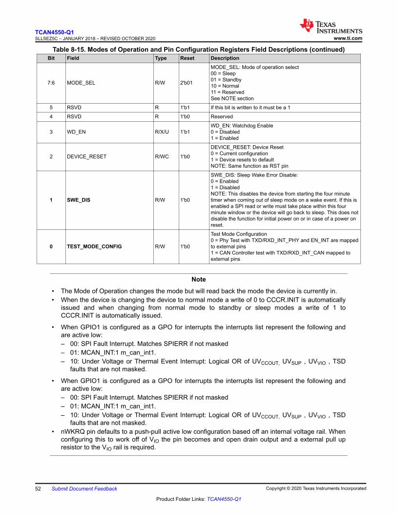
Table 8-15. Modes of Operation and Pin Configuration Registers Field Descriptions (continued)Bit Field Type Reset Description
7:6 MODE_SEL R/W 2'b01
MODE_SEL: Mode of operation select00 = Sleep01 = Standby10 = Normal11 = ReservedSee NOTE section
5 RSVD R 1'b1 If this bit is written to it must be a 1
4 RSVD R 1'b0 Reserved
3 WD_EN R/X/U 1’b1WD_EN: Watchdog Enable0 = Disabled1 = Enabled
2 DEVICE_RESET R/WC 1'b0
DEVICE_RESET: Device Reset0 = Current configuration1 = Device resets to defaultNOTE: Same function as RST pin
1 SWE_DIS R/W 1'b0
SWE_DIS: Sleep Wake Error Disable:0 = Enabled1 = DisabledNOTE: This disables the device from starting the four minutetimer when coming out of sleep mode on a wake event. If this isenabled a SPI read or write must take place within this fourminute window or the device will go back to sleep. This does notdisable the function for initial power on or in case of a power onreset.
0 TEST_MODE_CONFIG R/W 1'b0
Test Mode Configuration0 = Phy Test with TXD/RXD_INT_PHY and EN_INT are mappedto external pins1 = CAN Controller test with TXD/RXD_INT_CAN mapped toexternal pins
Note
• The Mode of Operation changes the mode but will read back the mode the device is currently in.• When the device is changing the device to normal mode a write of 0 to CCCR.INIT is automatically
issued and when changing from normal mode to standby or sleep modes a write of 1 toCCCR.INIT is automatically issued.
• When GPIO1 is configured as a GPO for interrupts the interrupts list represent the following andare active low:– 00: SPI Fault Interrupt. Matches SPIERR if not masked– 01: MCAN_INT:1 m_can_int1.– 10: Under Voltage or Thermal Event Interrupt: Logical OR of UVCCOUT, UVSUP , UVVIO , TSD
faults that are not masked.
• When GPIO1 is configured as a GPO for interrupts the interrupts list represent the following andare active low:– 00: SPI Fault Interrupt. Matches SPIERR if not masked– 01: MCAN_INT:1 m_can_int1.– 10: Under Voltage or Thermal Event Interrupt: Logical OR of UVCCOUT, UVSUP , UVVIO , TSD
faults that are not masked.• nWKRQ pin defaults to a push-pull active low configuration based off an internal voltage rail. When
configuring this to work off of VIO the pin becomes and open drain output and a external pull upresistor to the VIO rail is required.
TCAN4550-Q1SLLSEZ5C – JANUARY 2018 – REVISED OCTOBER 2020 www.ti.com
52 Submit Document Feedback Copyright © 2020 Texas Instruments Incorporated
Product Folder Links: TCAN4550-Q1

8.6.2.2 Timestamp Prescalar (address = h0804) [reset = h00000002]
Figure 8-24. Timestamp Prescalar31 30 29 28 27 26 25 24
RSVD
R
23 22 21 20 19 18 17 16
RSVD
R
15 14 13 12 11 10 9 8
RSVD
R
7 6 5 4 3 2 1 0
Timestamp Prescalar
R/W
Table 8-16. EMC Enhancement and Timestamp Prescalar Field DescriptionsBit Field Type Reset Description
31:24 RSVD R 8’h00 Reserved
23:16 RSVD R 8’h00 Reserved
15:8 RSVD R 8’h00 Reserved
7:0 Timestamp Prescalar R/W 8'h02Writing to this register resets the internal timestamp counter to 0and will set the internal CAN clock divider used for MCANTimestamp generation to (Timestamp Prescalar x 8)
www.ti.comTCAN4550-Q1
SLLSEZ5C – JANUARY 2018 – REVISED OCTOBER 2020
Copyright © 2020 Texas Instruments Incorporated Submit Document Feedback 53
Product Folder Links: TCAN4550-Q1

8.6.2.3 Test Register and Scratch Pad (address = h0808) [reset = h00000000]
Saved in sleep mode
Figure 8-25. Test and Scratch Pad Register31 30 29 28 27 26 25 24
Test Read and Write
R/W
23 22 21 20 19 18 17 16
Test Read and Write
R/W
15 14 13 12 11 10 9 8
Scratch Pad 1
R/W
7 6 5 4 3 2 1 0
Scratch Pad 2
R/W
Table 8-17. Test and Scratch Pad Register Field DescriptionsBit Field Type Reset Description
31:24 Test Read and Write RW 8’h00 Test Read and Write Register
23:16 Test Read and Write R/W 8’h00 Test Read and Write Register
15:8 Scratch Pad 1 R/W 8’h00 Bits 15:8 are saved when device is configured for sleep mode
7:0 Scratch Pad 2 R/W 8’h00 Bits 7:0 are saved when device is configured for sleep mode
TCAN4550-Q1SLLSEZ5C – JANUARY 2018 – REVISED OCTOBER 2020 www.ti.com
54 Submit Document Feedback Copyright © 2020 Texas Instruments Incorporated
Product Folder Links: TCAN4550-Q1

8.6.2.4 Test Register (address = h080C) [reset = h00000000]
Figure 8-26. Test Register31 30 29 28 27 26 25 24
RSVD
R
23 22 21 20 19 18 17 16
RSVD RSVD ECC_ERR_FORCE_BIT_SEL
R R R/W
15 14 13 12 11 10 9 8
RSVD RSVD ECC_ERR_FORCE
ECC_ERR_CHECK
RSVD RSVD RSVD
R R R/W R/W R R R
7 6 5 4 3 2 1 0
RSVD
R
Table 8-18. Test Register Field DescriptionsBit Field Type Reset Description
31:24 RSVD R 8’h00 Reserved
23:22 RSVD R 2'b00 Reserved
21:16 ECC_ERR_FORCE_BIT_SEL R/W
6’b000000
ECC_ERR_FORCE_BIT_SEL000000 = Bit 0000001 = Bit 1....100110 = Bit 38All other bit combinations are Reserved
15:13 RSVD R 3’b000 Reserved
12 ECC_ERR_FORCE R/W 1’b0ECC_ERR_FORCE0 = No Force1 = Force a single bit ECC error
11 ECC_ERR_CHECK R/W 1’b0ECC_ERR_CHECK0 = No Single Bit ECC error detected1 = Single Bit ECC error detected
10 RSVD R 1b'0 Reserved
9:0 RSVD R 10'b0000000000
Reserved
www.ti.comTCAN4550-Q1
SLLSEZ5C – JANUARY 2018 – REVISED OCTOBER 2020
Copyright © 2020 Texas Instruments Incorporated Submit Document Feedback 55
Product Folder Links: TCAN4550-Q1
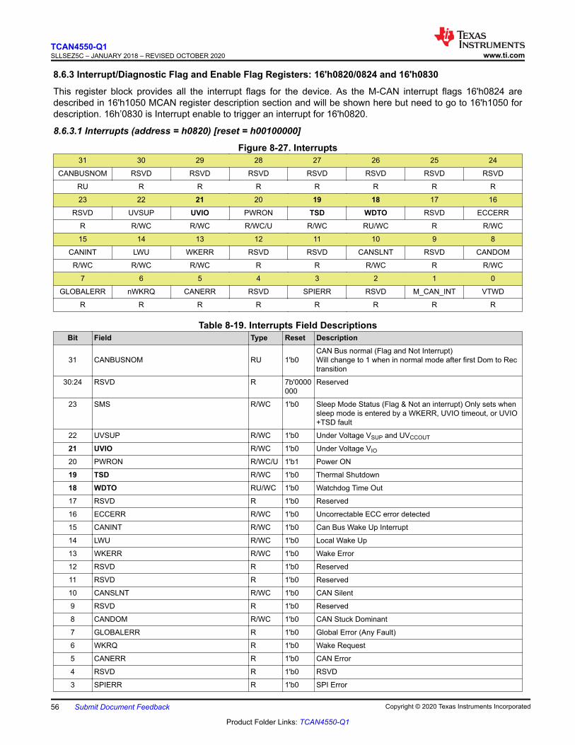
8.6.3 Interrupt/Diagnostic Flag and Enable Flag Registers: 16'h0820/0824 and 16'h0830
This register block provides all the interrupt flags for the device. As the M-CAN interrupt flags 16'h0824 aredescribed in 16'h1050 MCAN register description section and will be shown here but need to go to 16'h1050 fordescription. 16h’0830 is Interrupt enable to trigger an interrupt for 16'h0820.
8.6.3.1 Interrupts (address = h0820) [reset = h00100000]
Figure 8-27. Interrupts31 30 29 28 27 26 25 24
CANBUSNOM RSVD RSVD RSVD RSVD RSVD RSVD RSVD
RU R R R R R R R
23 22 21 20 19 18 17 16
RSVD UVSUP UVIO PWRON TSD WDTO RSVD ECCERR
R R/WC R/WC R/WC/U R/WC RU/WC R R/WC
15 14 13 12 11 10 9 8
CANINT LWU WKERR RSVD RSVD CANSLNT RSVD CANDOM
R/WC R/WC R/WC R R R/WC R R/WC
7 6 5 4 3 2 1 0
GLOBALERR nWKRQ CANERR RSVD SPIERR RSVD M_CAN_INT VTWD
R R R R R R R R
Table 8-19. Interrupts Field DescriptionsBit Field Type Reset Description
31 CANBUSNOM RU 1'b0CAN Bus normal (Flag and Not Interrupt)Will change to 1 when in normal mode after first Dom to Rectransition
30:24 RSVD R 7b'0000000
Reserved
23 SMS R/WC 1'b0 Sleep Mode Status (Flag & Not an interrupt) Only sets whensleep mode is entered by a WKERR, UVIO timeout, or UVIO+TSD fault
22 UVSUP R/WC 1'b0 Under Voltage VSUP and UVCCOUT
21 UVIO R/WC 1'b0 Under Voltage VIO
20 PWRON R/WC/U 1'b1 Power ON
19 TSD R/WC 1'b0 Thermal Shutdown
18 WDTO RU/WC 1'b0 Watchdog Time Out
17 RSVD R 1'b0 Reserved
16 ECCERR R/WC 1'b0 Uncorrectable ECC error detected
15 CANINT R/WC 1'b0 Can Bus Wake Up Interrupt
14 LWU R/WC 1'b0 Local Wake Up
13 WKERR R/WC 1'b0 Wake Error
12 RSVD R 1'b0 Reserved
11 RSVD R 1'b0 Reserved
10 CANSLNT R/WC 1'b0 CAN Silent
9 RSVD R 1'b0 Reserved
8 CANDOM R/WC 1'b0 CAN Stuck Dominant
7 GLOBALERR R 1'b0 Global Error (Any Fault)
6 WKRQ R 1'b0 Wake Request
5 CANERR R 1'b0 CAN Error
4 RSVD R 1'b0 RSVD
3 SPIERR R 1'b0 SPI Error
TCAN4550-Q1SLLSEZ5C – JANUARY 2018 – REVISED OCTOBER 2020 www.ti.com
56 Submit Document Feedback Copyright © 2020 Texas Instruments Incorporated
Product Folder Links: TCAN4550-Q1
Table 8-19. Interrupts Field Descriptions (continued)Bit Field Type Reset Description2 RSVD R 1'b0 Reserved
1 M_CAN_INT R 1'b0 M_CAN global INT
0 VTWD R 1'b0 Global Voltage, Temp or WDTO
GLOBALERR: Logical OR of all faults in registers 0x0820-0824.
WKRQ: Logical OR of CANINT, LWU and WKERR.
CANBUSNOM is not an interrupt but a flag. In normal mode after the first dominant-recessive transition it will set.It will reset to 0 when entering Standby or Sleep modes or when a bus fault condition takes place in normalmode.
CANERR: Logical OR of CANSLNT and CANDOM faults.
SPIERR: Will be set if any of the SPI status register 16'h000C[30:16] is set.• In the event of a SPI underflow, the error is not detected/alerted until the start of the next SPI transaction.• 16'h0010[30:16] are the mask for these errors
VTWD: Logical or of UVCCOUT , UVSUP, UVVIO, TSD, WDTO (Watchdog time out) and ECCERR.
CANINT: Indicates a WUP has occurred; Once a CANINT flag is set, LWU events will be ignored. Flag can becleared by changing to Normal or Sleep modes.
LWU: Indicates a local wake event, from toggling the WAKE pin, has occurred. Once a LWU flag is set, CANINTevents will be ignored. Flag can be cleared by changing to Normal or Sleep modes.
WKERR: If the device receives a wake up request WUP and does not transition to Normal mode or clear thePWRON or Wake flag before tINACTIVE, the device will transition to Sleep Mode. After the wake event, a WakeError (WKERR) will be reported and the SMS flag will be set to 1.
Note
PWRON Flag is cleared by either writing a 1 or by going to sleep mode or normal mode from standbymode.
www.ti.comTCAN4550-Q1
SLLSEZ5C – JANUARY 2018 – REVISED OCTOBER 2020
Copyright © 2020 Texas Instruments Incorporated Submit Document Feedback 57
Product Folder Links: TCAN4550-Q1
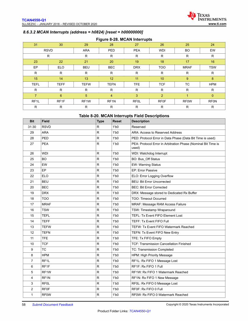
8.6.3.2 MCAN Interrupts (address = h0824) [reset = h00000000]
Figure 8-28. MCAN Interrupts31 30 29 28 27 26 25 24
RSVD ARA PED PEA WDI BO EW
R R R R R R R
23 22 21 20 19 18 17 16
EP ELO BEU BEC DRX TOO MRAF TSW
R R R R R R R R
15 14 13 12 11 10 9 8
TEFL TEFF TEFW TEFN TFE TCF TC HPM
R R R R R R R R
7 6 5 4 3 2 1 0
RF1L RF1F RF1W RF1N RF0L RF0F RF0W RF0N
R R R R R R R R
Table 8-20. MCAN Interrupts Field DescriptionsBit Field Type Reset Description
31:30 RSVD R 1'b0 Reserved
29 ARA R 1'b0 ARA: Access to Reserved Address
28 PED R 1'b0 PED: Protocol Error in Data Phase (Data Bit Time is used)
27 PEA R 1’b0 PEA: Protocol Error in Arbitration Phase (Nominal Bit Time isused)
26 WDI R 1'b0 WDI: Watchdog Interrupt
25 BO R 1'b0 BO: Bus_Off Status
24 EW R 1'b0 EW: Warning Status
23 EP R 1'b0 EP: Error Passive
22 ELO R 1'b0 ELO: Error Logging Overflow
21 BEU R 1'b0 BEU: Bit Error Uncorrected
20 BEC R 1'b0 BEC: Bit Error Corrected
19 DRX R 1’b0 DRX: Message stored to Dedicated Rx Buffer
18 TOO R 1'b0 TOO: Timeout Occurred
17 MRAF R 1'b0 MRAF: Message RAM Access Failure
16 TSW R 1'b0 TSW: Timestamp Wraparound
15 TEFL R 1'b0 TEFL: Tx Event FIFO Element Lost
14 TEFF R 1'b0 TEFF: Tx Event FIFO Full
13 TEFW R 1'b0 TEFW: Tx Event FIFO Watermark Reached
12 TEFN R 1'b0 TEFN: Tx Event FIFO New Entry
11 TFE R 1’b0 TFE: Tx FIFO Empty
10 TCF R 1'b0 TCF: Transmission Cancellation Finished
9 TC R 1'b0 TC: Transmission Completed
8 HPM R 1'b0 HPM: High Priority Message
7 RF1L R 1'b0 RF1L: Rx FIFO 1 Message Lost
6 RF1F R 1'b0 RF1F: Rx FIFO 1 Full
5 RF1W R 1'b0 RF1W: Rx FIFO 1 Watermark Reached
4 RF1N R 1'b0 RF1N: Rx FIFO 1 New Message
3 RF0L R 1’b0 RF0L: Rx FIFO 0 Message Lost
2 RF0F R 1'b0 RF0F: Rx FIFO 0 Full
1 RF0W R 1'b0 RF0W: Rx FIFO 0 Watermark Reached
TCAN4550-Q1SLLSEZ5C – JANUARY 2018 – REVISED OCTOBER 2020 www.ti.com
58 Submit Document Feedback Copyright © 2020 Texas Instruments Incorporated
Product Folder Links: TCAN4550-Q1
Table 8-20. MCAN Interrupts Field Descriptions (continued)Bit Field Type Reset Description0 RF0N R 1'b0 RF0N: Rx FIFO 0 New Message
www.ti.comTCAN4550-Q1
SLLSEZ5C – JANUARY 2018 – REVISED OCTOBER 2020
Copyright © 2020 Texas Instruments Incorporated Submit Document Feedback 59
Product Folder Links: TCAN4550-Q1

8.6.3.3 Interrupt Enables (address = h0830 ) [reset = hFFFFFFFF]
Figure 8-29. 32-bit, 4 Rows31 30 29 28 27 26 25 24
RSVD RSVD RSVD RSVD RSVD RSVD RSVD RSVD
R R R R R R R R
23 22 21 20 19 18 17 16
RSVD UVSUP UVIO RSVD TSD RSVD RSVD ECCERR
R R/W R/W R R/W R R R/W
15 14 13 12 11 10 9 8
CANINT LWU RSVD RSVD RSVD CANSLNT RSVD CANDOM
R/W R/W R R R R/W R R
7 6 5 4 3 2 1 0
RSVD
R
Table 8-21. Interrupt Enables Field DescriptionsBit Field Type Reset Description
31:24 RSVD R 8'hFF Reserved
23 RSVD R 1'b1 Reserved
22 UVSUP R/W 1'b1 Under Voltage VSUP and UVCC
21 UVIO R/W 1'b1 Under Voltage VIO
20 RSVD R 1'b1 Reserved
19 TSD R/W 1'b1 Thermal Shutdown
18 RSVD R 1'b1 Reserved
17 RSVD R 1'b1 Reserved
16 ECCERR R/W 1'b1 Uncorrectable ECC error detected
15 CANINT R/W 1'b1 Can Bus Wake Up Interrupt
14 LWU R/W 1'b1 Local Wake Up
13 RSVD R 1'b1 Reserved
12 RSVD R 1'b1 Reserved
11 RSVD R 1'b1 Reserved
10 CANSLNT R/W 1'b1 CAN Silent
9 RSVD R 1'b1 Reserved
8 CANDOM R/W 1'b1 CAN Stuck Dominant
7:0 RSVD R 8’hFF Reserved
TCAN4550-Q1SLLSEZ5C – JANUARY 2018 – REVISED OCTOBER 2020 www.ti.com
60 Submit Document Feedback Copyright © 2020 Texas Instruments Incorporated
Product Folder Links: TCAN4550-Q1

8.6.4 CAN FD Register Set: 16'h1000 to 16'h10FF
The following tables provide the CAN FD programming register sets starting at 16'h1000.
The MRAM and start address for the following registers has special consideration:• SIDFC (0x1084)• XIDFC (0x1088)• RXF0C (0x10A0)• RXF1C (0x10B0)• TXBC (0x10C0)• TXEFC (0x10F0)
The start address must be word aligned (32-bit) in the MRAM. The 2 least significant bits are ignored on a writeto ensure this behavior.
When entering the MRAM start address, the 0x8000 prefix is NOT necessary. For example, if the desired startaddress is 0x8634, then bits SA[15:0] will be 0x0634.
Table 8-22. LegendCode DescriptionR Read
C Clear on Write
d date
n Value after Reset
p Protected Set
P Protected Write
r Release
S Set on Read
t Test Value
U Undefined
W Write
X Reset on Read
Table 8-23. CAN FD Register SetADDRESS SYMBOL NAME RESET ACC
1000 CREL Core Release Register rrrd dddd R
1004 ENDN Endian Register 8765 4321 R
1008 CUST Customer Register 0000 0000 R
100C DBTP Data Bit Timing & Prescaler Register 0000 0A33 RP
1010 TEST Test Register 0000 0000 RP
1014 RWD RAM Watchdog 0000 0000 RP
1018 CCCR CC Control Register 0000 0019 RWPp
101C NBTP Nominal Bit Timing & Prescaler Register 0600 0A03 RP
1020 TSCC Timestamp Counter Configuration 0000 0000 RP
1024 TSCV Timestamp Counter Value 0000 0000 RC
1028 TOCC Timeout Counter Configuration FFFF 0000 RP
102C TOCV Timeout Counter Value 0000 FFFF RC
1030 RSVD Reserved 0000 0000 R
1034 RSVD Reserved 0000 0000 R
1038 RSVD Reserved 0000 0000 R
103C RSVD Reserved 0000 0000 R
www.ti.comTCAN4550-Q1
SLLSEZ5C – JANUARY 2018 – REVISED OCTOBER 2020
Copyright © 2020 Texas Instruments Incorporated Submit Document Feedback 61
Product Folder Links: TCAN4550-Q1

Table 8-23. CAN FD Register Set (continued)ADDRESS SYMBOL NAME RESET ACC
1040 ECR Error Counter Register 0000 0000 RX
1044 PSR Protocol Status Register 0000 0707 RXS
1048 TDCR Transmitter Delay Compensation Register 0000 0000 RP
104C RSVD Reserved 0000 0000 R
1050 IR Interrupt Register 0000 0000 RW
1054 IE Interrupt Enable 0000 0000 RW
1058 ILS Interrupt Line Select 0000 0000 RW
105C ILE Interrupt Line Enable 0000 0000 RW
1060 RSVD Reserved 0000 0000 R
1064 RSVD Reserved 0000 0000 R
1068 RSVD Reserved 0000 0000 R
106C RSVD Reserved 0000 0000 R
1070 RSVD Reserved 0000 0000 R
1074 RSVD Reserved 0000 0000 R
1078 RSVD Reserved 0000 0000 R
107C RSVD Reserved 0000 0000 R
1080 GFC Global Filter Configuration 0000 0000 RP
1084 SIDFC Standard ID Filter Configuration 0000 0000 RP
1088 XIDFC Extended ID Filter Configuration 0000 0000 RP
108C RSVD Reserved 0000 0000 R
1090 XIDAM Extended ID and MASK 1FFF FFFF RP
1094 HPMS High Priority Message Status 0000 0000 R
1098 NDAT1 New Data 1 0000 0000 RW
109C NDAT2 New Data 2 0000 0000 RW
10A0 RXF0C Rx FIFO 0 Configuration 0000 0000 RP
10A4 RXF0S Rx FIFO 0 Status 0000 0000 R
10A8 RXF0A Rx FIFO 0 Acknowledge 0000 0000 RW
10AC RXBC Rx Buffer Configuration 0000 0000 RP
10B0 RXF1C Rx FIFO 1 Configuration 0000 0000 RP
10B4 RXF1S Rx FIFO 1 Status 0000 0000 R
10B8 RXF1A Rx FIFO 1 Acknowledge 0000 0000 RW
10BC RXESC Rx Buffer/FIFO Element Size Configuration 0000 0000 RP
10C0 TXBC Tx Buffer Configuration 0000 0000 RP
10C4 TXFQS Tx FIFO/Queue Status 0000 0000 R
10C8 TXESC Tx Buffer Element Size Configuration 0000 0000 RP
10CC TXBRP Tx Buffer Request Pending 0000 0000 R
10D0 TXBAR Tx Buffer Add Request 0000 0000 RW
10D4 TXBCR Tx Buffer Cancellation Request 0000 0000 RW
10D8 TXBTO Tx Buffer Transmission Occurred 0000 0000 R
10DC TXBCF Tx Buffer Cancellation Finished 0000 0000 R
10E0 TXBTIE Tx Buffer Transmission Interrupt Enable 0000 0000 RW
10E4 TXBCIE Tx Buffer Cancellation Finished Interrupt Enable 0000 0000 RW
10E8 RSVD Reserved 0000 0000 R
10EC RSVD Reserved 0000 0000 R
10F0 TXEFC Tx Event FIFO Configuration 0000 0000 RP
TCAN4550-Q1SLLSEZ5C – JANUARY 2018 – REVISED OCTOBER 2020 www.ti.com
62 Submit Document Feedback Copyright © 2020 Texas Instruments Incorporated
Product Folder Links: TCAN4550-Q1
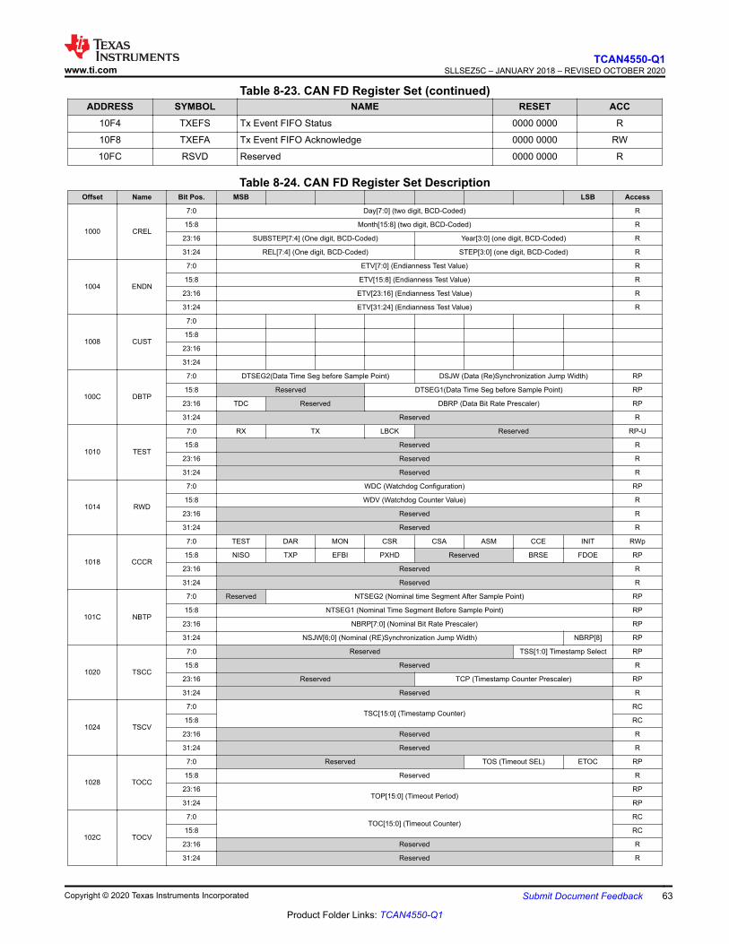
Table 8-23. CAN FD Register Set (continued)ADDRESS SYMBOL NAME RESET ACC
10F4 TXEFS Tx Event FIFO Status 0000 0000 R
10F8 TXEFA Tx Event FIFO Acknowledge 0000 0000 RW
10FC RSVD Reserved 0000 0000 R
Table 8-24. CAN FD Register Set DescriptionOffset Name Bit Pos. MSB LSB Access
1000 CREL
7:0 Day[7:0] (two digit, BCD-Coded) R
15:8 Month[15:8] (two digit, BCD-Coded) R
23:16 SUBSTEP[7:4] (One digit, BCD-Coded) Year[3:0] (one digit, BCD-Coded) R
31:24 REL[7:4] (One digit, BCD-Coded) STEP[3:0] (one digit, BCD-Coded) R
1004 ENDN
7:0 ETV[7:0] (Endianness Test Value) R
15:8 ETV[15:8] (Endianness Test Value) R
23:16 ETV[23:16] (Endianness Test Value) R
31:24 ETV[31:24] (Endianness Test Value) R
1008 CUST
7:0
15:8
23:16
31:24
100C DBTP
7:0 DTSEG2(Data Time Seg before Sample Point) DSJW (Data (Re)Synchronization Jump Width) RP
15:8 Reserved DTSEG1(Data Time Seg before Sample Point) RP
23:16 TDC Reserved DBRP (Data Bit Rate Prescaler) RP
31:24 Reserved R
1010 TEST
7:0 RX TX LBCK Reserved RP-U
15:8 Reserved R
23:16 Reserved R
31:24 Reserved R
1014 RWD
7:0 WDC (Watchdog Configuration) RP
15:8 WDV (Watchdog Counter Value) R
23:16 Reserved R
31:24 Reserved R
1018 CCCR
7:0 TEST DAR MON CSR CSA ASM CCE INIT RWp
15:8 NISO TXP EFBI PXHD Reserved BRSE FDOE RP
23:16 Reserved R
31:24 Reserved R
101C NBTP
7:0 Reserved NTSEG2 (Nominal time Segment After Sample Point) RP
15:8 NTSEG1 (Nominal Time Segment Before Sample Point) RP
23:16 NBRP[7:0] (Nominal Bit Rate Prescaler) RP
31:24 NSJW[6;0] (Nominal (RE)Synchronization Jump Width) NBRP[8] RP
1020 TSCC
7:0 Reserved TSS[1:0] Timestamp Select RP
15:8 Reserved R
23:16 Reserved TCP (Timestamp Counter Prescaler) RP
31:24 Reserved R
1024 TSCV
7:0TSC[15:0] (Timestamp Counter)
RC
15:8 RC
23:16 Reserved R
31:24 Reserved R
1028 TOCC
7:0 Reserved TOS (Timeout SEL) ETOC RP
15:8 Reserved R
23:16TOP[15:0] (Timeout Period)
RP
31:24 RP
102C TOCV
7:0TOC[15:0] (Timeout Counter)
RC
15:8 RC
23:16 Reserved R
31:24 Reserved R
www.ti.comTCAN4550-Q1
SLLSEZ5C – JANUARY 2018 – REVISED OCTOBER 2020
Copyright © 2020 Texas Instruments Incorporated Submit Document Feedback 63
Product Folder Links: TCAN4550-Q1

Table 8-24. CAN FD Register Set Description (continued)Offset Name Bit Pos. MSB LSB Access
1030 – 103C RSVD 31:0 Reserved R
TCAN4550-Q1SLLSEZ5C – JANUARY 2018 – REVISED OCTOBER 2020 www.ti.com
64 Submit Document Feedback Copyright © 2020 Texas Instruments Incorporated
Product Folder Links: TCAN4550-Q1

Table 8-24. CAN FD Register Set Description (continued)Offset Name Bit Pos. MSB LSB Access
1040 ECR
7:0 TEC (Transmit Error Counter) R
15:8 REC (Receive Error Counter) R
23:16 CEL (CAN Error Logging) X
31:24 Reserved R
1044 PSR
7:0 BO EW EP ACT (Activity) LEC (Last Error Code) RS
15:8 Reserved PXE RFDF RBRS RESI DLEC ( Data Phase Last Error Code) RSX
23:16 Reserved TDCV[6:0] (Transmitter Delay Compensation Value) R
31:24 Reserved R
1048 TDCR
7:0 Reserved TDCF (Transmitter Delay Compensation Filter Window Length) RP
15:8 Reserved TDCO (Transmitter Delay Compensation Offset) RP
23:16 Reserved R
31:24 Reserved R
104C RSVD 31:0 Reserved R
1050 IR
7:0 RF1L RF1F RF1W RF1N RF0L RF0F RF0W RF0N R/W
15:8 TEFL TEFF TEFW TEFN TFE TCF TC HPM R/W
23:16 EP ELO BEU BEC DRX TOO MRAF TSW R/W
31:24 Reserved ARA PED PEA WDI BO EW R/W
1054 IE
7:0 RF1LE RF1FE RF1WE RF1NE RF0LE RF0FE RF0WE RF0NE R/W
15:8 TEFLE TEFFE TEFWE TEFNE TFEE TCFE TCE HPME R/W
23:16 EPE ELOE BEUE BECE DRXE TOOE MRAFE TSWE R/W
31:24 Reserved ARAE PEDE PEAE WDIE BOE EWE R/W
1058 ILS
7:0 RF1LL RF1FL RF1WL RF1NL RF0LL RF0FL RF0WL RF0NL R/W
15:8 TEFLL TEFFL TEFWL TEFNL TFEL TCFL TCL HPML R/W
23:16 EPL ELOL BEUL BECL DRXL TOOL MRAFL TSWL R/W
31:24 Reserved ARAL PEDL PEAL WDIL BOL EWL R/W
105C ILE
7:0 Reserved EINT1 EINT0 R/W
15:8 Reserved R
23:16 Reserved R
31:24 Reserved R
1060 – 107C RSVD 31:0 Reserved R
1080 GFC
7:0 Reserved ANFS ANFE RRFS RRFE RP
15:8 Reserved R
23:16 Reserved R
31:24 Reserved R
1084 SIDFC
7:0 FLSS[7:2] (Filter List Standard Start Address) Reserved RP
15:8 FLSS[15:8] (Filter List Standard Start Address) RP
23:16 LSS (List Size Standard) RP
31:24 Reserved R
1088 XIDFC
7:0 FLESA[7:2] (Filter List Extended Start Address) Reserved RP
15:8 FLESA[15:8] (Filter List Extended Start Address) RP
23:16 Reserved LSE (List Size Extended) RP
31:24 Reserved R
108C RSVD 31:0 Reserved R
1090 XIDAM
7:0 EIDM[7:0] (Extended ID AND MASK) RP
15:8 EIDM[15:8] (Extended ID AND MASK) RP
23:16 EIDM[23:16] (Extended ID AND MASK) RP
31:24 Reserved EIDM[28:24] (Extended ID AND MASK) RP
1094 HPMS
7:0 MSI (Message StorageIndex) BIDX (Buffer Index) R
15:8 FLST FIDX (Filter Index) R
23:16 Reserved R
31:24 Reserved R
www.ti.comTCAN4550-Q1
SLLSEZ5C – JANUARY 2018 – REVISED OCTOBER 2020
Copyright © 2020 Texas Instruments Incorporated Submit Document Feedback 65
Product Folder Links: TCAN4550-Q1

Table 8-24. CAN FD Register Set Description (continued)Offset Name Bit Pos. MSB LSB Access
1098 NDAT1
7:0 ND7 ND6 ND5 ND4 ND3 ND2 ND1 ND0 R/W
15:8 ND15 ND14 ND13 ND12 ND11 ND10 ND9 ND8 R/W
23:16 ND23 ND22 ND21 ND20 ND19 ND18 ND17 ND16 R/W
31:24 ND31 ND30 ND29 ND28 ND27 ND26 ND25 ND24 R/W
109C NDAT2
7:0 ND39 ND38 ND37 ND36 ND35 ND34 ND33 ND32 R/W
15:8 ND47 ND46 ND45 ND44 ND43 ND42 ND41 ND40 R/W
23:16 ND55 ND54 ND53 ND52 ND51 ND50 ND49 ND48 R/W
31:24 ND63 ND62 ND61 ND60 ND59 ND58 ND57 ND56 R/W
10A0 RXF0C
7:0 F0SA[7:2] (RX FIFO 0 Start Address) Reserved RP
15:8 F0SA[15:8] (RX FIFO 0 Start Address) RP
23:16 Reserved F0S (RX FIFO 0 Size) RP
31:24 F0OM F0WM (RX FIFO 0 Watermark) RP
10A4 RXF0S
7:0 Reserved R
15:8 Reserved R
23:16 Reserved R
31:24 Reserved R
10A8 RXF0A
7:0 Reserved F0A (RX FIFO 0 Acknowledge Index) R/W
15:8 Reserved R
23:16 Reserved R
31:24 Reserved R
10AC RXBC
7:0 RBSA[7:2] (RX Buffer Configuration) Reserved RP
15:8 RBSA[15:8] (RX Buffer Configuration) RP
23:16 Reserved R
31:24 Reserved R
10B0 RXF1C
7:0 F1SA[7:2] (RX FIFO 1 Start Address) Reserved RP
15:8 F1SA[15:8] (RX FIFO 1 Start Address) RP
23:16 Reserved F1S (RX FIFO 1 Size) RP
31:24 F1OM F1WM (RX FIFO 1 Watermark) RP
10B4 RXF1S
7:0 Reserved F1FL (RX FIFO 1 Fill Level) R
15:8 Reserved F1GI (RX FIFO 1 Get Index) R
23:16 Reserved F1PI (RX FIFO 1 Put Index) R
31:24 DMS (Data Message Status) Reserved RF1L F1F R
10B8 RXF1A
7:0 Reserved F1AI (RX FIFO 1 Acknowledge Index) R/W
15:8 Reserved R
23:16 Reserved R
31:24 Reserved R
10BC RXESC
7:0 Reserved F1DS (RX FIFO 1 Data Field Size) Reserved F0DS (RX FIFO 0 Data Field Size) RP
15:8 Reserved RBDS (RX Buffer Data Field Size) RP
23:16 Reserved R
31:24 Reserved R
10C0 TXBC
7:0 TBSA[7:2] (TX Buffer Start Address) Reserved RP
15:8 TBSA[15:8] (TX Buffer Start Address) RP
23:16 Reserved NDTB (Number of Dedicated Transmit Buffers) RP
31:24 Reserved TFQM TFQS (Transmit FIFO/Queue Size) RP
10C4 TXQFS
7:0 Reserved TFFL (TX FIFO Free Level) R
15:8 Reserved TFGI (TX FIFO Get Index) R
23:16 Reserved TFQF TFQP (TX FIFO/Queue Put Index) R
31:24 Reserved R
10C8 TXESC
7:0 Reserved TBDS (TX Buffer Data Field Size) RP
15:8 Reserved R
23:16 Reserved R
31:24 Reserved R
TCAN4550-Q1SLLSEZ5C – JANUARY 2018 – REVISED OCTOBER 2020 www.ti.com
66 Submit Document Feedback Copyright © 2020 Texas Instruments Incorporated
Product Folder Links: TCAN4550-Q1
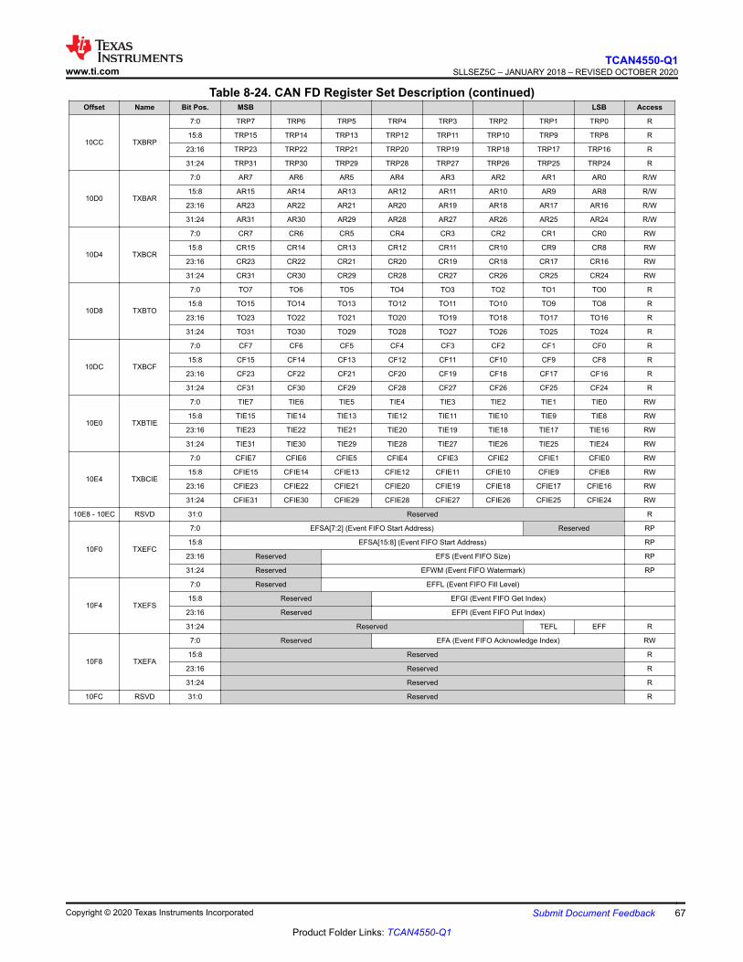
Table 8-24. CAN FD Register Set Description (continued)Offset Name Bit Pos. MSB LSB Access
10CC TXBRP
7:0 TRP7 TRP6 TRP5 TRP4 TRP3 TRP2 TRP1 TRP0 R
15:8 TRP15 TRP14 TRP13 TRP12 TRP11 TRP10 TRP9 TRP8 R
23:16 TRP23 TRP22 TRP21 TRP20 TRP19 TRP18 TRP17 TRP16 R
31:24 TRP31 TRP30 TRP29 TRP28 TRP27 TRP26 TRP25 TRP24 R
10D0 TXBAR
7:0 AR7 AR6 AR5 AR4 AR3 AR2 AR1 AR0 R/W
15:8 AR15 AR14 AR13 AR12 AR11 AR10 AR9 AR8 R/W
23:16 AR23 AR22 AR21 AR20 AR19 AR18 AR17 AR16 R/W
31:24 AR31 AR30 AR29 AR28 AR27 AR26 AR25 AR24 R/W
10D4 TXBCR
7:0 CR7 CR6 CR5 CR4 CR3 CR2 CR1 CR0 RW
15:8 CR15 CR14 CR13 CR12 CR11 CR10 CR9 CR8 RW
23:16 CR23 CR22 CR21 CR20 CR19 CR18 CR17 CR16 RW
31:24 CR31 CR30 CR29 CR28 CR27 CR26 CR25 CR24 RW
10D8 TXBTO
7:0 TO7 TO6 TO5 TO4 TO3 TO2 TO1 TO0 R
15:8 TO15 TO14 TO13 TO12 TO11 TO10 TO9 TO8 R
23:16 TO23 TO22 TO21 TO20 TO19 TO18 TO17 TO16 R
31:24 TO31 TO30 TO29 TO28 TO27 TO26 TO25 TO24 R
10DC TXBCF
7:0 CF7 CF6 CF5 CF4 CF3 CF2 CF1 CF0 R
15:8 CF15 CF14 CF13 CF12 CF11 CF10 CF9 CF8 R
23:16 CF23 CF22 CF21 CF20 CF19 CF18 CF17 CF16 R
31:24 CF31 CF30 CF29 CF28 CF27 CF26 CF25 CF24 R
10E0 TXBTIE
7:0 TIE7 TIE6 TIE5 TIE4 TIE3 TIE2 TIE1 TIE0 RW
15:8 TIE15 TIE14 TIE13 TIE12 TIE11 TIE10 TIE9 TIE8 RW
23:16 TIE23 TIE22 TIE21 TIE20 TIE19 TIE18 TIE17 TIE16 RW
31:24 TIE31 TIE30 TIE29 TIE28 TIE27 TIE26 TIE25 TIE24 RW
10E4 TXBCIE
7:0 CFIE7 CFIE6 CFIE5 CFIE4 CFIE3 CFIE2 CFIE1 CFIE0 RW
15:8 CFIE15 CFIE14 CFIE13 CFIE12 CFIE11 CFIE10 CFIE9 CFIE8 RW
23:16 CFIE23 CFIE22 CFIE21 CFIE20 CFIE19 CFIE18 CFIE17 CFIE16 RW
31:24 CFIE31 CFIE30 CFIE29 CFIE28 CFIE27 CFIE26 CFIE25 CFIE24 RW
10E8 - 10EC RSVD 31:0 Reserved R
10F0 TXEFC
7:0 EFSA[7:2] (Event FIFO Start Address) Reserved RP
15:8 EFSA[15:8] (Event FIFO Start Address) RP
23:16 Reserved EFS (Event FIFO Size) RP
31:24 Reserved EFWM (Event FIFO Watermark) RP
10F4 TXEFS
7:0 Reserved EFFL (Event FIFO Fill Level)
15:8 Reserved EFGI (Event FIFO Get Index)
23:16 Reserved EFPI (Event FIFO Put Index)
31:24 Reserved TEFL EFF R
10F8 TXEFA
7:0 Reserved EFA (Event FIFO Acknowledge Index) RW
15:8 Reserved R
23:16 Reserved R
31:24 Reserved R
10FC RSVD 31:0 Reserved R
www.ti.comTCAN4550-Q1
SLLSEZ5C – JANUARY 2018 – REVISED OCTOBER 2020
Copyright © 2020 Texas Instruments Incorporated Submit Document Feedback 67
Product Folder Links: TCAN4550-Q1

8.6.4.1 Core Release Register (address = h1000) [reset = hrrrddddd]
Figure 8-30. Core Release Register31 30 29 28 27 26 25 24
REL[3:0] STEP[3:0]
R R
23 22 21 20 19 18 17 16
SUBSTEP[3:0] YEAR[3:0]
R R
15 14 13 12 11 10 9 8
MONTH[7:0]
R
7 6 5 4 3 2 1 0
DAY[7:0]
R
Table 8-25. Core Release Register Field DescriptionsBit Field Type Reset Description
31:28 REL[3:0] R r one digit, BCD-coded
27:24 STEP[3:0] R r one digit, BCD-coded
23:20 SUBSTEP[3:0] R r one digit, BCD-coded
19:16 YEAR[3:0] R d one digit, BCD-coded
15:8 MONTH[7:0] R d two digit, BCD-coded
7:0 DAY[7:0] R d two digit, BCD-coded
TCAN4550-Q1SLLSEZ5C – JANUARY 2018 – REVISED OCTOBER 2020 www.ti.com
68 Submit Document Feedback Copyright © 2020 Texas Instruments Incorporated
Product Folder Links: TCAN4550-Q1

8.6.4.2 Endian Register (address = h1004) [reset = h87654321]
Figure 8-31. Endian Register31 30 29 28 27 26 25 24
ETV[31:24]
R
23 22 21 20 19 18 17 16
ETV[23:16]
R
15 14 13 12 11 10 9 8
ETV[15:8]
R
7 6 5 4 3 2 1 0
ETV[7:0]
R
Table 8-26. Endian Register Field DescriptionsBit Field Type Reset Description
31:24 ETV[31:24] R 0x87 Endianness Test Value
23:16 ETV[23:16] R 0x65 Endianness Test Value
15:8 ETV[15:8] R 0x43 Endianness Test Value
7:0 ETV[7:0] R 0x21 Endianness Test Value
www.ti.comTCAN4550-Q1
SLLSEZ5C – JANUARY 2018 – REVISED OCTOBER 2020
Copyright © 2020 Texas Instruments Incorporated Submit Document Feedback 69
Product Folder Links: TCAN4550-Q1
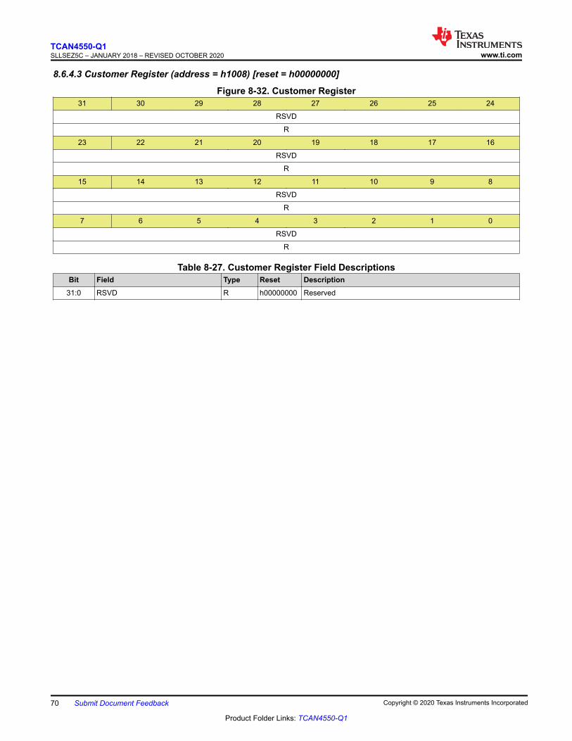
8.6.4.3 Customer Register (address = h1008) [reset = h00000000]
Figure 8-32. Customer Register31 30 29 28 27 26 25 24
RSVD
R
23 22 21 20 19 18 17 16
RSVD
R
15 14 13 12 11 10 9 8
RSVD
R
7 6 5 4 3 2 1 0
RSVD
R
Table 8-27. Customer Register Field DescriptionsBit Field Type Reset Description
31:0 RSVD R h00000000 Reserved
TCAN4550-Q1SLLSEZ5C – JANUARY 2018 – REVISED OCTOBER 2020 www.ti.com
70 Submit Document Feedback Copyright © 2020 Texas Instruments Incorporated
Product Folder Links: TCAN4550-Q1

8.6.4.4 Data Bit Timing & Prescaler (address = h100C) [reset = h0000A33]
Figure 8-33. Data Bit Timing & Prescaler31 30 29 28 27 26 25 24
RSVD
R
23 22 21 20 19 18 17 16
TDC RSVD DBRP[4:0]
n R RP
15 14 13 12 11 10 9 8
RSVD DTSEG1[4:0]
R RP
7 6 5 4 3 2 1 0
DTSEG2[3:0] DSJW[3:0]
RP RP
Table 8-28. Data Bit Timing & Prescaler Field DescriptionsBit Field Type Reset Description
31:24 RSVD R 0x0 Reserved
23 TDC RP 0x0Transmitter Delay Compensation0 – TDC Disabled1 – TDC Enabled
22:21 RSVD R 0x0 Reserved
20:16 DBRP[4:0] RP 0x0 Data Bit Rate Prescaler
15:13 RSVD R 0x0 Reserved
12:8 DTSEG1[4:0] RP 0xA Data time Segment before sample point
7:4 DTSEG2[3:0] RP 0x3 Data time Segment before sample point
3:0 DSJW[3:0] RP 0x3 Data (Re)Synchronization Jump Width
www.ti.comTCAN4550-Q1
SLLSEZ5C – JANUARY 2018 – REVISED OCTOBER 2020
Copyright © 2020 Texas Instruments Incorporated Submit Document Feedback 71
Product Folder Links: TCAN4550-Q1
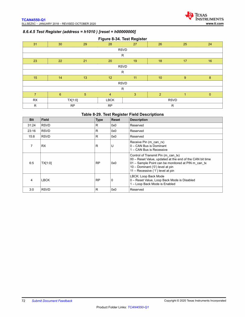
8.6.4.5 Test Register (address = h1010 ) [reset = h00000000]
Figure 8-34. Test Register31 30 29 28 27 26 25 24
RSVD
R
23 22 21 20 19 18 17 16
RSVD
R
15 14 13 12 11 10 9 8
RSVD
R
7 6 5 4 3 2 1 0
RX TX[1:0] LBCK RSVD
R RP RP R
Table 8-29. Test Register Field DescriptionsBit Field Type Reset Description
31:24 RSVD R 0x0 Reserved
23:16 RSVD R 0x0 Reserved
15:8 RSVD R 0x0 Reserved
7 RX R UReceive Pin (m_can_rx)0 – CAN Bus is Dominant1 – CAN Bus is Recessive
6:5 TX[1:0] RP 0x0
Control of Transmit Pin (m_can_tx)00 – Reset Value, updated at the end of the CAN bit time01 – Sample Point can be monitored at PIN m_can_tx10 – Dominant (‘0’) level at pin11 – Recessive (‘1’) level at pin
4 LBCK RP 0LBCK: Loop Back Mode0 – Reset Value, Loop Back Mode is Disabled1 – Loop Back Mode is Enabled
3:0 RSVD R 0x0 Reserved
TCAN4550-Q1SLLSEZ5C – JANUARY 2018 – REVISED OCTOBER 2020 www.ti.com
72 Submit Document Feedback Copyright © 2020 Texas Instruments Incorporated
Product Folder Links: TCAN4550-Q1

8.6.4.6 RAM Watchdog (address = h1014) [reset = h00000000]
Figure 8-35. RAM Watchdog31 30 29 28 27 26 25 24
RSVD
R
23 22 21 20 19 18 17 16
RSVD
R
15 14 13 12 11 10 9 8
WDV[7:0]
R
7 6 5 4 3 2 1 0
WDC[7:0]
RP
Table 8-30. RAM Watchdog Field DescriptionsBit Field Type Reset Description
31:24 RSVD R 0x0 Reserved
23:16 RSVD R 0x0 Reserved
15:8 WDV[7:0] R 0x0 Watchdog Counter Value
7:0 WDC[7:0] RP 0x0 Watchdog Configuration
www.ti.comTCAN4550-Q1
SLLSEZ5C – JANUARY 2018 – REVISED OCTOBER 2020
Copyright © 2020 Texas Instruments Incorporated Submit Document Feedback 73
Product Folder Links: TCAN4550-Q1

8.6.4.7 Control Register (address = h1018) [reset = 0000 0019]
Figure 8-36. Control Register31 30 29 28 27 26 25 24
RSVD
R
23 22 21 20 19 18 17 16
RSVD
R
15 14 13 12 11 10 9 8
NISO TXP EFBI PXHD RSVD BRSE FDOE
RP RP RP RP R RP RP
7 6 5 4 3 2 1 0
TEST DAR MON CSR CSA ASM CCE INIT
Rp RP Rp R/W R Rp RP R/W
Table 8-31. Control Register Field DescriptionsBit Field Type Reset Description
31:24 RSVD R 0x0 Reserved
23:16 RSVD R 0x0 Reserved
15 NISO RP 0
Non ISO Operation0 – CAN FD Frame format according to ISO 11898-1:20151 – CAN FD Frame format according to Bosch CAN FDSpecification V1.0
14 TXP RP 0Transmitter Pause0 – Transmitter Pause Disabled1 – Transmitter Pause Enabled
13 EFBI RP 0
Edge Filtering during Bus Integration0 – Edge Filtering Disabled1 – Two Consecutive Dominant tq required to detect an edge forhard synchronization
12 PXHD RP 0Protocol Exception Handling Disable0 – Protocol Exception Handling Enabled1 – Protocol Exception Handling Disabled
11:10 RSVD R 0x0 Reserved
9 BRSE RP 0Bit Rate Switch Enable0 – Bit Rate Switching for Transmission Disabled1 – Bit Rate Switching for Transmission Enabled
8 FDOE RP 0FD Operation Enable0 – FD Operation Disabled1 – FD Operation Enabled
7 TEST Rp 0
Test Mode Enable0 – Normal Mode of Operation, Register TEST Holds ResetValue1 – Test Mode, Write Access to Register TEST Enabled
6 DAR RP 0
Disable Automatic Retransmission0 – Automatic Retransmission of Messages not TransmittedSuccessfully Enabled1 – Automatic Retransmission Disabled
5 MON Rp 0Bus Monitoring Mode is Disabled0 – Bus Monitoring Mode is Disabled1 – Bus Monitoring Mode is Enabled
TCAN4550-Q1SLLSEZ5C – JANUARY 2018 – REVISED OCTOBER 2020 www.ti.com
74 Submit Document Feedback Copyright © 2020 Texas Instruments Incorporated
Product Folder Links: TCAN4550-Q1

Table 8-31. Control Register Field Descriptions (continued)Bit Field Type Reset Description
4 CSR R/W 1
Clock Stop Request0 – No clock Stop is requested1 – Clock Stop Requested. When requested first INIT and thenCSA will be set after all pending transfer request havecompleted and the CAN bus reached idleSee NOTE section
3 CSA R 1
Clock Stop Acknowledge0 – No Clock Stop Requested1 – m_can may be set in power down by stopping m_can-hclkand m_can_cclk
2 ASM Rp 0Restricted Operation Mode0 – Normal CAN Operation1 – Restricted Operation Mode Active
1 CCE RP 0
Configuration Change Enable0 – CPU has no write access to the protected configurationregisters1 – CPU has write access to the protected configurationregisters (While CCCR.INIT =1)
0 INIT R/W 1Initialization0 – Normal Operation1 – Initialization has started
Note
The TCAN4550-Q1 handles stop request through hardware. The means that a 1 should not be writtento CCCR.CSR (Clock Stop Request) as this will interfere with normal operation. If a Read-Modify-Write operation is performed in Standby mode a CSR = 1 will be read back but a 0 should be writtento it.
www.ti.comTCAN4550-Q1
SLLSEZ5C – JANUARY 2018 – REVISED OCTOBER 2020
Copyright © 2020 Texas Instruments Incorporated Submit Document Feedback 75
Product Folder Links: TCAN4550-Q1

8.6.4.8 Nominal Bit Timing & Prescaler Register (address = h101C) [reset = h06000A03]
Figure 8-37. Nominal Bit Timing & Prescaler Register31 30 29 28 27 26 25 24
NSJW[6:0] NBRP[8]
RP RP
23 22 21 20 19 18 17 16
NBRP[7:0]
RP
15 14 13 12 11 10 9 8
NTSEG1[7:0]
RP
7 6 5 4 3 2 1 0
RSVD NTSEG2[6:0]
R RP
Table 8-32. Nominal Bit Timing & Prescaler Register Field DescriptionsBit Field Type Reset Description
31:25 NSJW[6:0] RP 0x3
Nominal (RE)Synchronization Jump Width0x00 - 0x7F – Valid values are 0 to 127 - The actualinterpretation by the hardware of this value is such that onemore than the value programmed here is used.
24:16 NBRP[8:0] RP 0x0
Nominal Bit Rate Prescaler0x000 - 0x1FF – Value by which the oscillator frequency isdivided for generating the bit time quanta. Valid values are 0 to511. - The actual interpretation by the hardware of this value issuch that one more than the value programmed here is used.
15:8 NTSEG1[7:0] RP 0xA
Nominal Time Segment Before Sample Point)0x01-0xFF – Valid values are 1 to 255 - The actual interpretationby the hardware of this value is such that one more than thevalue programmed here is used.
7 RSVD R 0 Reserved
6:0 NTSEG2[6:0] RP 0x3
Nominal Time Segment After Sample Point0x01-0x7F – Valid values are 1 to 127 - The actual interpretationby the hardware of this value is such that one more than thevalue programmed here is used.
TCAN4550-Q1SLLSEZ5C – JANUARY 2018 – REVISED OCTOBER 2020 www.ti.com
76 Submit Document Feedback Copyright © 2020 Texas Instruments Incorporated
Product Folder Links: TCAN4550-Q1

8.6.4.9 Timestamp Counter Configuration (address = h1020) [reset = h00000000]
Figure 8-38. Timestamp Counter Configuration31 30 29 28 27 26 25 24
RSVD
R
23 22 21 20 19 18 17 16
RSVD TCP[3:0]
R RP
15 14 13 12 11 10 9 8
RSVD
R
7 6 5 4 3 2 1 0
RSVD TSS[1:0]
R RP
Table 8-33. Timestamp Counter Configuration DescriptionsBit Field Type Reset Description
31:24 RSVD R 0x0 Reserved
23:20 RSVD R 0x0 Reserved
19:16 TCP[3:0] RP 0x0Timestamp Counter Prescaler0x0 - 0xF – Configures timestamp and timeout counters timeunit in multiples of CAN bit times [1…16]
15:8 RSVD R 0x0 Reserved
7:2 RSVD R 0x0 Reserved
1:0 TSS[1:0] RP 0x0
Timestamp Select00 – Timestamp counter value always 0x000001 – Timestamp counter value incremented according to TCP10 – External timestamp counter value used11 – Same as "00"
www.ti.comTCAN4550-Q1
SLLSEZ5C – JANUARY 2018 – REVISED OCTOBER 2020
Copyright © 2020 Texas Instruments Incorporated Submit Document Feedback 77
Product Folder Links: TCAN4550-Q1

8.6.4.10 Timestamp Counter Value (address = h1024) [reset = h00000000]
Figure 8-39. Timestamp Counter Value31 30 29 28 27 26 25 24
RSVD
R
23 22 21 20 19 18 17 16
RSVD
R
15 14 13 12 11 10 9 8
TSC[15:8]
RC
7 6 5 4 3 2 1 0
TSC[7:0]
RC
Table 8-34. Timestamp Counter Value Field DescriptionsBit Field Type Reset Description
31:24 RSVD R 0x0 Reserved
23:20 RSVD R 0x0 Reserved
15:8
TSC[7:0] RC 0x0
Timestamp CounterThe internal/external Timestamp Counter value is captured onstart of frame (both Rx and Tx). When TSCC.TSS = “01”, theTimestamp Counter is incremented in multiples of CAN bit times[1…16] depending on the configuration of TSCC.TCP. A wraparound sets interrupt flag IR.TSW. Write access resets thecounter to zero. When TSCC.TSS = “10”, TSC reflects theexternalTimestamp Counter value. A write access has no impact.
7:0
TSC[7:0] RC 0x0
Timestamp CounterThe internal/external Timestamp Counter value is captured onstart of frame (both Rx and Tx). When TSCC.TSS = “01”, theTimestamp Counter is incremented in multiples of CAN bit times[1…16] depending on the configuration of TSCC.TCP. A wraparound sets interrupt flag IR.TSW. Write access resets thecounter to zero. When TSCC.TSS = “10”, TSC reflects theexternalTimestamp Counter value. A write access has no impact.
TCAN4550-Q1SLLSEZ5C – JANUARY 2018 – REVISED OCTOBER 2020 www.ti.com
78 Submit Document Feedback Copyright © 2020 Texas Instruments Incorporated
Product Folder Links: TCAN4550-Q1

8.6.4.11 Timeout Counter Configuration (address = h1028) [reset = hFFFF0000]
Figure 8-40. Timeout Counter Configuration31 30 29 28 27 26 25 24
TOP[15:8]
R
23 22 21 20 19 18 17 16
TOP[7:0]
R
15 14 13 12 11 10 9 8
RSVD
R
7 6 5 4 3 2 1 0
RSVD TOS[1:0] ETOC
R RP RP
Table 8-35. Timeout Counter Configuration Field DescriptionsBit Field Type Reset Description
31:24 TOP[15:8] RP 0xFFTimeout PeriodStart value of the timeout counter (down-counter). Configuresthe timeout period
23:16 TOP[7:0] RP 0xFFTimeout PeriodStart value of the timeout counter (down-counter). Configuresthe timeout period
15:8 RSVD R 0x0 Reserved
7:3 RSVD R 0x0 Reserved
2:1 TOS[1:0] RP 0x0
Timeout SelectWhen operating in Continuous mode, a write to TOCV presetsthe counter to the value configured by TOCC.TOP andcontinues down-counting. When the Timeout Counter iscontrolled by one of the FIFOs, an empty FIFO presets thecounter to the value configured by TOCC.TOP. Down-counting isstarted when the first FIFO element is stored00 – Continuous Operation01 – Timeout controlled by TX Event FIFO10 – Timeout controlled by Rx FIFO 011 – Timeout controlled by Rx FIFO 1
0 ETOC RP 0Enable Timeout Counter0 – Timeout counter disabled1 – Timeout counter enabled
www.ti.comTCAN4550-Q1
SLLSEZ5C – JANUARY 2018 – REVISED OCTOBER 2020
Copyright © 2020 Texas Instruments Incorporated Submit Document Feedback 79
Product Folder Links: TCAN4550-Q1

8.6.4.12 Timeout Counter Value (address = h102C) [reset = h0000FFFF]
Figure 8-41. Timeout Counter Value31 30 29 28 27 26 25 24
RSVD
R
23 22 21 20 19 18 17 16
RSVD
R
15 14 13 12 11 10 9 8
TOC[15:8]
RC
7 6 5 4 3 2 1 0
TOC[7:0]
RC
Table 8-36. Timeout Counter Value Field DescriptionsBit Field Type Reset Description
31:24 RSVD R 0x0 Reserved
23:16 RSVD R 0x0 Reserved
15:8 TOC[15:8] RC 0xFF
Timeout CounterThe Timeout Counter is decremented in multiples of CAN bittimes [1…16] depending on the configuration of TSCC.TCP.When decremented to zero, interrupt flag IR.TOO is set and theTimeout Counter is stopped. Start and reset/restart conditionsare configured via TOCC.TOS
7:0 TOC[7:0] RC 0xFF
Timeout CounterThe Timeout Counter is decremented in multiples of CAN bittimes [1…16] depending on the configuration of TSCC.TCP.When decremented to zero, interrupt flag IR.TOO is set and theTimeout Counter is stopped. Start and reset/restart conditionsare configured via TOCC.TOS
TCAN4550-Q1SLLSEZ5C – JANUARY 2018 – REVISED OCTOBER 2020 www.ti.com
80 Submit Document Feedback Copyright © 2020 Texas Instruments Incorporated
Product Folder Links: TCAN4550-Q1
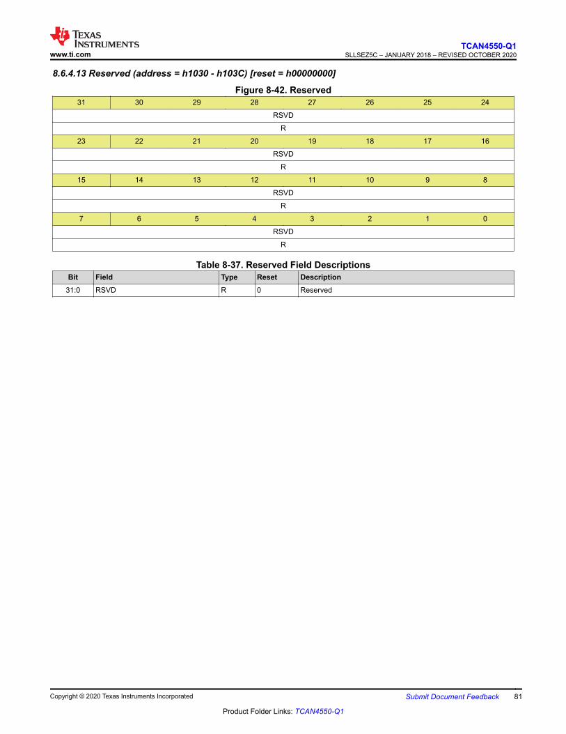
8.6.4.13 Reserved (address = h1030 - h103C) [reset = h00000000]
Figure 8-42. Reserved31 30 29 28 27 26 25 24
RSVD
R
23 22 21 20 19 18 17 16
RSVD
R
15 14 13 12 11 10 9 8
RSVD
R
7 6 5 4 3 2 1 0
RSVD
R
Table 8-37. Reserved Field DescriptionsBit Field Type Reset Description
31:0 RSVD R 0 Reserved
www.ti.comTCAN4550-Q1
SLLSEZ5C – JANUARY 2018 – REVISED OCTOBER 2020
Copyright © 2020 Texas Instruments Incorporated Submit Document Feedback 81
Product Folder Links: TCAN4550-Q1

8.6.4.14 Error Counter Register (address = h1040) [reset = h00000000]
Figure 8-43. Error Counter Register31 30 29 28 27 26 25 24
RSVD
R
23 22 21 20 19 18 17 16
CEL[7:0]
X
15 14 13 12 11 10 9 8
RP REC[6:0]
R R
7 6 5 4 3 2 1 0
TEC[7:0]
R
Table 8-38. Error Counter Register Field DescriptionsBit Field Type Reset Description
31:24 RSVD R 0x0 Reserved
23:16 CEL[7:0] X 0x0
CAN Error LoggingThe counter is incremented each time when a CAN protocolerror causes the Transmit Error Counter or the Receive ErrorCounter to be incremented. It is reset by read access to CEL.The counter stops at 0xFF; the next increment of TEC or RECsets interrupt flag IR.ELO
15 RP R 0
0 – The Receive Error Counter is below the error passive levelof 1281 – The Receive Error Counter has reached the error passivelevel of 128
14:8 REC[6:0] R 0x0 Actual state of the Receive Error Counter, values between 0 and127
7:0 TEC[7:0] R 0x0 Actual state of the Transmit Error Counter, values between 0and 255
Note
When CCCR.ASM is set, the CAN protocol controller does not increment TEC and REC when a CANprotocol error is detected, but CEL is still incremented.
TCAN4550-Q1SLLSEZ5C – JANUARY 2018 – REVISED OCTOBER 2020 www.ti.com
82 Submit Document Feedback Copyright © 2020 Texas Instruments Incorporated
Product Folder Links: TCAN4550-Q1

8.6.4.15 Protocol Status Register (address = h1044) [reset = h00000707]
Figure 8-44. Protocol Status Register31 30 29 28 27 26 25 24
RSVD
R
23 22 21 20 19 18 17 16
RSVD TDCV[6:0]
R R
15 14 13 12 11 10 9 8
RSVD PXE RFDF RBRS RESI DLEC[2:0]
R X X X X S
7 6 5 4 3 2 1 0
BO EW EP ACT[1:0] LEC[2:0]
R R R R S
Table 8-39. Protocol Status Register Field DescriptionsBit Field Type Reset Description
31:24 RSVD R 0x0 Reserved
23 RSVD R 0x0 Reserved
22:16 TDCV[6:0] R 0x0
Transmitter Delay Compensation Value0x00-0x7F – Position of the secondary sample point, defined bythe sum of the measured delay from m_can_tx to m_can_rx andTDCR.TDCO. The SSP position is, in the data phase, thenumber of mtq between the start of the transmitted bit and thesecondary sample point. Valid values are 0 to 127 mtq.
15 RSVD R 0 Reserved
14 PXE X 0Protocol Exception Event0 – No protocol exception event occurred since last read access1 – Protocol exception event occurred
13 RFDF X 0
Received a CAN FD MessageThis bit is set independent of acceptance filtering0 – Since this bit was reset by the CPU, no CAN FD messagehas been received1 – Message in CAN FD format with FDF flag set has beenreceived
12 RBRS X 0
BRS flag of last received CAN FD MessageThis bit is set together with RFDF, independent of acceptancefiltering.0 – Last received CAN FD message did not have its BRS flagset1 – Last received CAN FD message had its BRS flag set
11 RESI X 0
ESI flag of last received CAN FD MessageThis bit is set together with RFDF, independent of acceptancefiltering.0 – Last received CAN FD message did not have its ESI flag set1 – Last received CAN FD message had its ESI flag set
10:8 DLEC[2:0] X 0x7
Data Phase Last Error CodeType of last error that occurred in the data phase of a CAN FDformat frame with its BRS flag set. Coding is the same as forLEC. This field will be cleared to zero when a CAN FD formatframe with its BRS flag set has been transferred (reception ortransmission) without error.
7 BO R 0Bus_Off Status0 – The M_CAN is not Bus_Off1 – The M_CAN is in Bus_Off state
www.ti.comTCAN4550-Q1
SLLSEZ5C – JANUARY 2018 – REVISED OCTOBER 2020
Copyright © 2020 Texas Instruments Incorporated Submit Document Feedback 83
Product Folder Links: TCAN4550-Q1
Table 8-39. Protocol Status Register Field Descriptions (continued)Bit Field Type Reset Description
6 EW R 0
Warning Status0 – Both error counters are below the Error_Warning limit of 961 – At least one of error counter has reached the Error_Warninglimit of 96
5 EP R 0
Error Passive0 – The M_CAN is in the Error_Active state. It normally takespart in bus communication and sends an active error flag whenan error has been detected1 – The M_CAN is in the Error_Passive state
4:3 ACT[1:0] R 0x0
ActivityMonitors the module’s CAN communication state.00 – Synchronizing - node is synchronizing on CANcommunication01 – Idle - node is neither receiver nor transmitter10 – Receiver - node is operating as receiver11 – Transmitter - node is operating as transmitter
2:0 LEC[2:0] S 0x7
Last Error CodeThe LEC indicates the type of the last error to occur on the CANbus. This field will be cleared to ‘0’ when a message has beentransferred (reception or transmission) without error.0 – No Error: No error occurred since LEC has been reset bysuccessful reception or transmission1 – Stuff Error: More than 5 equal bits in a sequence haveoccurred in a part of a received message where this is notallowed.2 – Form Error: A fixed format part of a received frame has thewrong format.3 – AckError: The message transmitted by the M_CAN was notacknowledged by another node.4 – Bit1Error: During the transmission of a message (with theexception of the arbitration field), the device wanted to send arecessive level (bit of logical value ‘1’), but the monitored busvalue was dominant.5 – Bit0Error: During the transmission of a message (oracknowledge bit, or active error flag, or overload flag), thedevice wanted to send a dominant level (data or identifier bitlogical value ‘0’), but the monitored bus value was recessive.During Bus_Off recovery this status is set each time a sequenceof 11 recessive bits has been monitored. This enables the CPUto monitor the proceeding of the Bus_Off recovery sequence(indicating the bus is not stuck at dominant or continuouslydisturbed).6 – CRCError: The CRC check sum of a received message wasincorrect. The CRC of an incoming message does not matchwith the CRC calculated from the received data.7 – NoChange: Any read access to the Protocol Status Registerre-initializes the LEC to ‘7’. When the LEC shows the value ‘7’,no CAN bus event was detected since the last CPU read accessto the Protocol Status Register.
Note
When a frame in CAN FD format has reached the data phase with BRS flag set, the next CAN event(error or valid frame) will be shown in DLEC instead of LEC. An error in a fixed stuff bit of a CAN FDCRC sequence will be shown as a Form Error, not Stuff Error
TCAN4550-Q1SLLSEZ5C – JANUARY 2018 – REVISED OCTOBER 2020 www.ti.com
84 Submit Document Feedback Copyright © 2020 Texas Instruments Incorporated
Product Folder Links: TCAN4550-Q1

Note
The Bus_Off recovery sequence (see ISO 11898-1:2015) cannot be shortened by setting or resettingCCCR.INIT. If the device goes Bus_Off, it will set CCCR.INIT of its own accord, stopping all busactivities. Once CCCR.INIT has been cleared by the CPU, the device will then wait for 129occurrences of Bus Idle (129 * 11 consecutive recessive bits) before resuming normal operation. Atthe end of the Bus_Off recovery sequence, the Error Management Counters will be reset. During thewaiting time after the resetting of CCCR.INIT, each time a sequence of 11 recessive bits has beenmonitored, a Bit0Error code is written to PSR.LEC, enabling the CPU to readily checkup whether theCAN bus is stuck at dominant or continuously disturbed and to monitor the Bus_Off recoverysequence. ECR.REC is used to count these sequences.
www.ti.comTCAN4550-Q1
SLLSEZ5C – JANUARY 2018 – REVISED OCTOBER 2020
Copyright © 2020 Texas Instruments Incorporated Submit Document Feedback 85
Product Folder Links: TCAN4550-Q1
8.6.4.16 Transmitter Delay Compensation Register (address = h1048) [reset = h00000000]
Figure 8-45. Transmitter Delay Compensation Register31 30 29 28 27 26 25 24
RSVD
R
23 22 21 20 19 18 17 16
RSVD
R
15 14 13 12 11 10 9 8
RSVD TDCO[6:0]
R RP
7 6 5 4 3 2 1 0
RSVD TDCF[6:0]
R RP
Table 8-40. Transmitter Delay Compensation Register Field DescriptionsBit Field Type Reset Description
31:24 RSVD R 0x0 Reserved
23:16 RSVD R 0x0 Reserved
15 RSVD R 0 Reserved
14:8 TDCO[6:0] RP 0x0
Transmitter Delay Compensation Offset0x00-0x7F - Offset value defining the distance between themeasured delay from m_can_tx to m_can_rx and the secondarysample point. Valid values are 0 to 127 mtq.
7 RSVD R 0 Reserved
6:0 TDCF[6:0] RP 0x0
Transmitter Delay Compensation Filter Window Length0x00-0x7F - Defines the minimum value of the SSP position,dominant edges on m_can_rx that would result in an earlier SSPposition are ignored for transmitter delay measurement. Thefeature is enabled when TDCF is configured to a value greaterthan TDCO. Valid values are 0 to 127 mtq.
TCAN4550-Q1SLLSEZ5C – JANUARY 2018 – REVISED OCTOBER 2020 www.ti.com
86 Submit Document Feedback Copyright © 2020 Texas Instruments Incorporated
Product Folder Links: TCAN4550-Q1

8.6.4.17 Reserved (address = h104C) [reset = h00000000]
Figure 8-46. Reserved31 30 29 28 27 26 25 24
RSVD
R
23 22 21 20 19 18 17 16
RSVD
R
15 14 13 12 11 10 9 8
RSVD
R
7 6 5 4 3 2 1 0
RSVD
R
Table 8-41. Reserved Field DescriptionsBit Field Type Reset Description
31:0 RSVD R 0 Reserved
www.ti.comTCAN4550-Q1
SLLSEZ5C – JANUARY 2018 – REVISED OCTOBER 2020
Copyright © 2020 Texas Instruments Incorporated Submit Document Feedback 87
Product Folder Links: TCAN4550-Q1

8.6.4.18 Interrupt Register (address = h1050) [reset = h00000000]
Figure 8-47. Interrupt Register31 30 29 28 27 26 25 24
RSVD ARA PED PEA WDI BO EW
R R/W R/W R/W R/W R/W R/W
23 22 21 20 19 18 17 16
EP ELO BEU BEC DRX TOO MRF TSW
R/W R/W R/W R/W R/W R/W R/W R/W
15 14 13 12 11 10 9 8
TEFL TEFF TEFW TEFN TFE TCF TC HPM
R/W R/W R/W R/W R/W R/W R/W R/W
7 6 5 4 3 2 1 0
RF1L RF1F RF1W RF1N RF0L RF0F RF0W RF0N
R/W R/W R/W R/W R/W R/W R/W R/W
Table 8-42. Interrupt Register Field DescriptionsBit Field Type Reset Description
31:30 RSVD R 0x0 Reserved
29 ARA R/W 0Access to Reserved Address0 – No access to reserved address occurred1 – Access to reserved address occurred
28 PED R/W 0Protocol Error in Data Phase (Data Bit Time is used)0 – No protocol error in data phase1 – Protocol error in data phase detected (PSR.DLEC ≠ 0,7)
27 PEA R/W 0Protocol Error in Arbitration Phase (Nominal Bit Time is used)0 – No protocol error in arbitration phase1 – Protocol error in arbitration phase detected (PSR.LEC ≠ 0,7)
26 WDI R/W 0Watchdog Interrupt0 – No Message RAM Watchdog event occurred1 – Message RAM Watchdog event due to missing READY
25 BO R/W 0Bus_Off Status0 – Bus_Off status unchanged1 – Bus_Off status changed
24 EW R/W 0Warning Status0 – Error_Warning status unchanged1 – Error_Warning status changed
23 EP R/W 0Error Passive0 – Error_Passive status unchanged1 – Error_Passive status changed
22 ELO R/W 0ELO: Error Logging Overflow0 – CAN Error Logging Counter did not overflow1 – Overflow of CAN Error Logging Counter occurred
21 BEU R/W 0
Bit Error UncorrectedMessage RAM bit error detected, uncorrected. Controlled byinput signal m_can_aeim_berr[1] generated by an optionalexternal parity / ECC logic attached to the Message RAM. Anuncorrected Message RAM bit error sets CCCR.INIT to ‘1’. Thisis done to avoid transmission of corrupted data.0 – No bit error detected when reading from Message RAM1 – Bit error detected, uncorrected (e.g. parity logic)
20 BEC R/W 0
Bit Error CorrectedMessage RAM bit error detected and corrected. Controlled byinput signal m_can_aeim_berr[0] generated by an optionalexternal parity / ECC logic attached to the Message RAM.0 – No bit error detected when reading from Message RAM1 – Bit error detected and corrected (e.g. ECC)
TCAN4550-Q1SLLSEZ5C – JANUARY 2018 – REVISED OCTOBER 2020 www.ti.com
88 Submit Document Feedback Copyright © 2020 Texas Instruments Incorporated
Product Folder Links: TCAN4550-Q1

Table 8-42. Interrupt Register Field Descriptions (continued)Bit Field Type Reset Description
19 DRX R/W 0
Message stored to Dedicated Rx BufferThe flag is set whenever a received message has been storedinto a dedicated Rx Buffer.0 – No Rx Buffer updated1 – At least one received message stored into an Rx Buffer
18 TOO R/W 0Timeout Occurred0 – No timeout1 – Timeout reached
17 MRF R/W 0
Message RAM Access FailureThe flag is set, when the Rx Handler• has not completed acceptance filtering or storage of an
accepted message until the arbitration field of the followingmessage has been received. In this case acceptancefiltering or message storage is aborted and the Rx Handlerstart processing of the following message
• was not able to write a message to the Message RAM. Inthis case message storage is aborted.
In both cases the FIFO put index is not updated resp. the NewData flag for a dedicated Rx Buffer is not set, a partly storedmessage is overwritten when the next message is stored to thislocation. The flag is also set when the Tx Handler was not ableto read a message from the Message RAM in time. In this casemessage transmission is aborted. In case of a Tx Handleraccess failure the M_CAN is switched into Restricted OperationMode. To leave restricted Operation Mode, the Host CPU has toreset CCCR.ASM.0 – No Message RAM access failure occurred1 – Message RAM access failure occurred
16 TSW R/W 0Timestamp Wraparound0 – No timestamp counter wrap-around1 – Timestamp counter wrapped aroundo
15 TEFL R/W 0
Tx Event FIFO Element Lost0 – No Tx Event FIFO element lost1 – Tx Event FIFO element lost, also set after write attempt toTx Event FIFO of size zero
14 TEFF R/W 0Tx Event FIFO Full0 – Tx Event FIFO not full1 – Tx Event FIFO full
13 TEFW R/W 0Tx Event FIFO Watermark Reached0 – Tx Event FIFO fill level below watermark1 – Tx Event FIFO fill level reached watermark
12 TEFN R/W 0Tx Event FIFO New Entry0 – Tx Event FIFO unchanged1 – Tx Handler wrote Tx Event FIFO element
11 TFE R/W 0Tx FIFO Empty0 – Tx FIFO non-empty1 – Tx FIFO empty
10 TCF R/W 0Transmission Cancellation Finished0 – No transmission cancellation finished1 – Transmis
9 TC R/W 0Transmission Completed0 – No transmission completed1 – Transmission completed
8 HPM R/W 0High Priority Message0 – No high priority message received1 – High priority message received
www.ti.comTCAN4550-Q1
SLLSEZ5C – JANUARY 2018 – REVISED OCTOBER 2020
Copyright © 2020 Texas Instruments Incorporated Submit Document Feedback 89
Product Folder Links: TCAN4550-Q1

Table 8-42. Interrupt Register Field Descriptions (continued)Bit Field Type Reset Description
7 RF1L R/W 0
Rx FIFO 1 Message Lost0 – No Rx FIFO 1 message lost1 – Rx FIFO 1 message lost, also set after write attempt to RxFIFO 1 of size zero
6 RF1F R/W 0Rx FIFO 1 Full0 – Rx FIFO 1 not full1 – Rx FIFO 1 full
5 RF1W R/W 0Rx FIFO 1 Watermark Reached0 – Rx FIFO 1 fill level below watermark1 – Rx FIFO 1 fill level reached watermark
4 RF1N R/W 0Rx FIFO 1 New Message0 – No new message written to Rx FIFO1 – New message written to Rx FIFO 1
3 RF0L R/W 0
Rx FIFO 0 Message Lost0 – No Rx FIFO 0 message lost1 – Rx FIFO 0 message lost, also set after write attempt to RxFIFO 0 of size zero
2 RF0F R/W 0Rx FIFO 0 Full0 – Rx FIFO 0 not full1 – Rx FIFO 0 full
1 RF0W R/W 0Rx FIFO 0 Watermark Reached0 – Rx FIFO 0 fill level below watermark1 – Rx FIFO 0 fill level reached watermark
0 RF0N R/W 0Rx FIFO 0 New Message0 – No new message written to Rx FIFO 01 – New message written to Rx FIFO 0
TCAN4550-Q1SLLSEZ5C – JANUARY 2018 – REVISED OCTOBER 2020 www.ti.com
90 Submit Document Feedback Copyright © 2020 Texas Instruments Incorporated
Product Folder Links: TCAN4550-Q1

8.6.4.19 Interrupt Enable (address = h1054) [reset = h00000000]
The settings in the Interrupt Enable register determine which status changes in the Interrupt Register will besignaled on an interrupt line.• 0 – Interrupt disabled• 1 – Interrupt enabled
Figure 8-48. Interrupt Enable Register31 30 29 28 27 26 25 24
RSVD ARAE PEDE PEAE WDIE BOE EWE
R R/W R/W R/W R/W R/W R/W
23 22 21 20 19 18 17 16
EPE ELOE BEUE BECE DRXE TOOE MRAFE TSWE
R/W R/W R/W R/W R/W R/W R/W R/W
15 14 13 12 11 10 9 8
TEFLE TEFFE TEFW TEFNE TFEE TCFE TCE HPME
R/W R/W R/W R/W R/W R/W R/W R/W
7 6 5 4 3 2 1 0
RF1LE RF1FE RF1WE RF1NE RF0LE RF0FE RF0WE RF0NE
R/W R/W R/W R/W R/W R/W R/W R/W
Table 8-43. Interrupt Enable Field DescriptionsBit Field Type Reset Description
31:30 RSVD R 0x0 Reserved
29 ARAE R/W 0 Access to Reserved Address Enable
28 PEDE R/W 0 Protocol Error in Data Phase Enable
27 PEAE R/W 0 Protocol Error in Arbitration Phase Enable
26 WDIE R/W 0 Watchdog Interrupt Enable
25 BOE R/W 0 Bus_Off Status Interrupt Enable
24 EWE R/W 0 Warning Status Interrupt Enable
23 EPE R/W 0 Error Passive Interrupt Enable
22 ELOE R/W 0 Error Logging Overflow Interrupt Enable
21 BEUE R/W 0 Bit Error Uncorrected Interrupt Enable
20 BECE R/W 0 Bit Error Corrected Interrupt Enable
19 DRXE R/W 0 Message stored to Dedicated Rx Buffer Interrupt Enable
18 TOOE R/W 0 Timeout Occurred Interrupt Enable
17 MRAFE R/W 0 Message RAM Access Failure Interrupt Enable
16 TSWE R/W 0 Timestamp Wraparound Interrupt Enable
15 TEFLE R/W 0 Tx Event FIFO Event Lost Interrupt Enable
14 TEFFE R/W 0 Tx Event FIFO Full Interrupt Enable
13 TEFW R/W 0 Tx Event FIFO Watermark Reached Interrupt Enable
12 TEFNE R/W 0 Tx Event FIFO New Entry Interrupt Enable
11 TFEE R/W 0 Tx FIFO Empty Interrupt Enable
10 TCFE R/W 0 Transmission Cancellation Finished Interrupt Enable
9 TCE R/W 0 Transmission Completed Interrupt Enable
8 HPME R/W 0 High Priority Message Interrupt Enable
7 RF1LE R/W 0 Rx FIFO 1 Message Lost Interrupt Enable
6 RF1FE R/W 0 Rx FIFO 1 Full Interrupt Enable
5 RF1WE R/W 0 Rx FIFO 1 Watermark Reached Interrupt Enable
www.ti.comTCAN4550-Q1
SLLSEZ5C – JANUARY 2018 – REVISED OCTOBER 2020
Copyright © 2020 Texas Instruments Incorporated Submit Document Feedback 91
Product Folder Links: TCAN4550-Q1

Table 8-43. Interrupt Enable Field Descriptions (continued)Bit Field Type Reset Description4 RF1NE R/W 0 Rx FIFO 1 New Message Interrupt Enable
3 RF0LE R/W 0 Rx FIFO 0 Message Lost Interrupt Enable
2 RF0FE R/W 0 Rx FIFO 0 Full Interrupt Enable
1 RF0WE R/W 0 Rx FIFO 0 Watermark Reached Interrupt Enable
0 RF0NE R/W 0 Rx FIFO 0 New Message Interrupt Enable
TCAN4550-Q1SLLSEZ5C – JANUARY 2018 – REVISED OCTOBER 2020 www.ti.com
92 Submit Document Feedback Copyright © 2020 Texas Instruments Incorporated
Product Folder Links: TCAN4550-Q1

8.6.4.20 Interrupt Line Select (address = h1058) [reset = h00000000]
The Interrupt Line Select register assigns an interrupt generated by a specific interrupt flag from the InterruptRegister to one of the two module interrupt lines. For interrupt generation the respective interrupt line has to beenabled via ILE.EINT0 and ILE.EINT1.• 0 – Interrupt assigned to interrupt line m_can_int0• 1 – Interrupt assigned to interrupt line m_can_int1
Figure 8-49. Interrupt Line Select Register31 30 29 28 27 26 25 24
RSVD ARAL PEDL PEAL WDIL BOL EWL
R R/W R/W R/W R/W R/W R/W
23 22 21 20 19 18 17 16
EPL ELOL BEUL BECL DRXL TOOL MRAFL TSWL
R/W R/W R/W R/W R/W R/W R/W R/W
15 14 13 12 11 10 9 8
TEFLL TEFFL TEFWL TEFNL TFEL TCFL TCL HPML
R/W R/W R/W R/W R/W R/W R/W R/W
7 6 5 4 3 2 1 0
RF1LL RF1FL RF1WL RF1NL RF0LL RF0FL RF0WL RF0NL
R/W R/W R/W R/W R/W R/W R/W R/W
Table 8-44. Interrupt Line Select Field DescriptionsBit Field Type Reset Description
31:30 RSVD R 0x0 Reserved
29 ARAL R/W 0 Access to Reserved Address Line
28 PEDL R/W 0 Protocol Error in Data Phase Line
27 PEAL R/W 0 Protocol Error in Arbitration Phase Line
26 WDIL R/W 0 Watchdog Interrupt Line
25 BOL R/W 0 Bus_Off Status Interrupt Line
24 EWL R/W 0 Warning Status Interrupt Line
23 EPL R/W 0 Error Passive Interrupt Line
22 ELOL R/W 0 Error Logging Overflow Interrupt Line
21 BEUL R/W 0 Bit Error Uncorrected Interrupt Line
20 BECL R/W 0 Bit Error Corrected Interrupt Line
19 DRXL R/W 0 Message stored to Dedicated Rx Buffer Interrupt Line
18 TOOL R/W 0 Timeout Occurred Interrupt Line
17 MRAFL R/W 0 Message RAM Access Failure Interrupt Line
16 TSWL R/W 0 Timestamp Wraparound Interrupt Line
15 TEFLL R/W 0 Tx Event FIFO Event Lost Interrupt Line
14 TEFFL R/W 0 Tx Event FIFO Full Interrupt Line
13 TEFWL R/W 0 Tx Event FIFO Watermark Reached Interrupt Line
12 TEFNL R/W 0 Tx Event FIFO New Entry Interrupt Line
11 TFEL R/W 0 Tx FIFO Empty Interrupt Line
10 TCFL R/W 0 Transmission Cancellation Finished Interrupt Line
9 TCL R/W 0 Transmission Completed Interrupt Line
8 HPML R/W 0 High Priority Message Interrupt Line
7 RF1LL R/W 0 Rx FIFO 1 Message Lost Interrupt Line
6 RF1FL R/W 0 Rx FIFO 1 Full Interrupt Line
www.ti.comTCAN4550-Q1
SLLSEZ5C – JANUARY 2018 – REVISED OCTOBER 2020
Copyright © 2020 Texas Instruments Incorporated Submit Document Feedback 93
Product Folder Links: TCAN4550-Q1

Table 8-44. Interrupt Line Select Field Descriptions (continued)Bit Field Type Reset Description5 RF1WL R/W 0 Rx FIFO 1 Watermark Reached Interrupt Line
4 RF1NL R/W 0 Rx FIFO 1 New Message Interrupt Line
3 RF0LL R/W 0 Rx FIFO 0 Message Lost Interrupt Line
2 RF0FL R/W 0 Rx FIFO 0 Full Interrupt Line
1 RF0WL R/W 0 Rx FIFO 0 Watermark Reached Interrupt Line
0 RF0NL R/W 0 Rx FIFO 0 New Message Interrupt Line
TCAN4550-Q1SLLSEZ5C – JANUARY 2018 – REVISED OCTOBER 2020 www.ti.com
94 Submit Document Feedback Copyright © 2020 Texas Instruments Incorporated
Product Folder Links: TCAN4550-Q1

8.6.4.21 Interrupt Line Enable (address = h105C) [reset = h00000000]
Figure 8-50. Interrupt Line Enable Register31 30 29 28 27 26 25 24
RSVD
R
23 22 21 20 19 18 17 16
RSVD
R
15 14 13 12 11 10 9 8
RSVD
R
7 6 5 4 3 2 1 0
RSVD EINT1 EINT0
R R/W R/W
Table 8-45. Interrupt Line Enable Field DescriptionsBit Field Type Reset Description
31:24 RSVD R 0x0 Reserved
23:16 RSVD R 0x0 Reserved
15:8 RSVD R 0x0 Reserved
7:2 RSVD R 0x0 Reserved
1 EINT1 R/W 0Enable Interrupt Line 10 - Interrupt line m_can_int1 disabled1 - Interrupt line m_can_int1 enabled
0 EINT0 R/w 0Enable Interrupt Line 00 - Interrupt line m_can_int0 disabled1 - Interrupt line m_can_int0 enabled
www.ti.comTCAN4550-Q1
SLLSEZ5C – JANUARY 2018 – REVISED OCTOBER 2020
Copyright © 2020 Texas Instruments Incorporated Submit Document Feedback 95
Product Folder Links: TCAN4550-Q1

8.6.4.22 Reserved (address = h1060 - h107C) [reset = h00000000]
Figure 8-51. Reserved31 30 29 28 27 26 25 24
RSVD
R
23 22 21 20 19 18 17 16
RSVD
R
15 14 13 12 11 10 9 8
RSVD
R
7 6 5 4 3 2 1 0
RSVD
R
Table 8-46. Reserved Field DescriptionsBit Field Type Reset Description
31:0 RSVD R 0 Reserved
TCAN4550-Q1SLLSEZ5C – JANUARY 2018 – REVISED OCTOBER 2020 www.ti.com
96 Submit Document Feedback Copyright © 2020 Texas Instruments Incorporated
Product Folder Links: TCAN4550-Q1

8.6.4.23 Global Filter Configuration (address = h1080) [reset = h00000000]
Figure 8-52. Global Filter Configuration Register31 30 29 28 27 26 25 24
RSVD
R
23 22 21 20 19 18 17 16
RSVD
R
15 14 13 12 11 10 9 8
RSVD
R
7 6 5 4 3 2 1 0
RSVD ANFS[1:0] ANFE[1:0] RRFS RRFE
R RP RP RP RP
Table 8-47. Global Filter Configuration Field DescriptionsBit Field Type Reset Description
31:24 RSVD R 0x0 Reserved
23:16 RSVD R 0x0 Reserved
15:8 RSVD R 0x0 Reserved
7:6 RSVD R 0x0 Reserved
5:4 ANFS[1:0] RP 0x0
Accept Non-matching Frames StandardDefines how received messages with 11-bit IDs that do notmatch any element of the filter list are treated.00 - Accept in Rx FIFO 001 - Accept in Rx FIFO 110 - Reject11 - Reject
3:2 ANFE[1:0] RP 0x0
Accept Non-matching Frames ExtendedDefines how received messages with 29-bit IDs that do notmatch any element of the filter list are treated.00 - Accept in Rx FIFO 001 - Accept in Rx FIFO 110 - Reject11 - Reject
1 RRFS RP 0Reject Remote Frames Standard0 - Filter remote frames with 11-bit standard IDs1 - Reject all remote frames with 11-bit standard IDs
0 RRFE RP 0Reject Remote Frames Extended0 - Filter remote frames with 29-bit extended IDs1 - Reject all remote frames with 29-bit extended IDs
www.ti.comTCAN4550-Q1
SLLSEZ5C – JANUARY 2018 – REVISED OCTOBER 2020
Copyright © 2020 Texas Instruments Incorporated Submit Document Feedback 97
Product Folder Links: TCAN4550-Q1
8.6.4.24 Standard ID Filter Configuration (address = h1084) [reset = h00000000]
The MRAM and start address for this register, FLSSA, has special consideration.• The start address must be word aligned (32-bit) in the MRAM. The 2 least significant bits are ignored on a
write to ensure this behavior.• When entering the MRAM start address, the 0x8000 prefix is NOT necessary. For example, if the desired
start address is 0x8634, then bits SA[15:0] will be 0x0634.
Figure 8-53. Standard ID Filter Configuration Register31 30 29 28 27 26 25 24
RSVD
R
23 22 21 20 19 18 17 16
LSS[7:0]
RP
15 14 13 12 11 10 9 8
FLSSA[15:8]
RP
7 6 5 4 3 2 1 0
FLSSA[7:0]
RP
Table 8-48. Standard ID Filter Configuration Field DescriptionsBit Field Type Reset Description
31:24 RSVD R 0x0 Reserved
23:16 LSS[7:0] RP 0x0
List Size Standard0 - No standard Message ID filter1-128 - Number of standard Message ID filter elements>128 - Values greater than 128 are interpreted as 128
15:0 FLSSA[15:0] RP 0x0 Filter List Standard Start AddressStart address of standard Message ID filter list
TCAN4550-Q1SLLSEZ5C – JANUARY 2018 – REVISED OCTOBER 2020 www.ti.com
98 Submit Document Feedback Copyright © 2020 Texas Instruments Incorporated
Product Folder Links: TCAN4550-Q1

8.6.4.25 Extended ID Filter Configuration (address = h1088) [reset = h00000000]
The MRAM and start address for this register, FLSEA, has special consideration.• The start address must be word aligned (32-bit) in the MRAM. The 2 least significant bits are ignored on a
write to ensure this behavior.• When entering the MRAM start address, the 0x8000 prefix is NOT necessary. For example, if the desired
start address is 0x8634, then bits SA[15:0] will be 0x0634.
Figure 8-54. Extended ID Filter Configuration Register31 30 29 28 27 26 25 24
RSVD
R
23 22 21 20 19 18 17 16
RSVD LSE[6:0]
R RP
15 14 13 12 11 10 9 8
FLSEA[15:8]
RP
7 6 5 4 3 2 1 0
FLSEA[7:0]
RP
Table 8-49. Extended ID Filter Configuration Field DescriptionsBit Field Type Reset Description
31:24 RSVD R 0x0 Reserved
23 RSVD R 0 Reserved
22:16 LSE[6:0] RP 0x0
List Size Extended0 - No extended Message ID filter1-64 - Number of extended Message ID filter elements>64 - Values greater than 64 are interpreted as 64
15:0 FLSEA[15:0] RP 0x0 Filter List Extended Start AddressStart address of extended Message ID filter list
www.ti.comTCAN4550-Q1
SLLSEZ5C – JANUARY 2018 – REVISED OCTOBER 2020
Copyright © 2020 Texas Instruments Incorporated Submit Document Feedback 99
Product Folder Links: TCAN4550-Q1

8.6.4.26 Reserved (address = h108C) [reset = h00000000]
Figure 8-55. Reserved31 30 29 28 27 26 25 24
RSVD
R
23 22 21 20 19 18 17 16
RSVD
R
15 14 13 12 11 10 9 8
RSVD
R
7 6 5 4 3 2 1 0
RSVD
R
Table 8-50. Reserved Field DescriptionsBit Field Type Reset Description
31:0 RSVD R 0 Reserved
TCAN4550-Q1SLLSEZ5C – JANUARY 2018 – REVISED OCTOBER 2020 www.ti.com
100 Submit Document Feedback Copyright © 2020 Texas Instruments Incorporated
Product Folder Links: TCAN4550-Q1

8.6.4.27 Extended ID AND Mask (address = h1090) [reset = h1FFFFFFF]
Figure 8-56. Extended ID AND Mask Register31 30 29 28 27 26 25 24
RSVD EIDM[28:24]
R RP
23 22 21 20 19 18 17 16
EIDM[23:16]
RP
15 14 13 12 11 10 9 8
EIDM[15:8]
RP
7 6 5 4 3 2 1 0
RP-0xFF
RP
Table 8-51. Extended ID AND Mask Field DescriptionsBit Field Type Reset Description
31:30 RSVD R 2'b00 Reserved
29:24 EIDM[28:24] RP 6'b011111
Extended ID MaskFor acceptance filtering of extended frames the Extended IDAND Mask is ANDed with the Message ID of a received frame.Intended for masking of 29-bit IDs in SAE J1939. With the resetvalue of all bits set to one the mask is not active.
23:0 EIDM[23:16] to EIDM[7:0] RP 0xFFFFFF
Extended ID MaskFor acceptance filtering of extended frames the Extended IDAND Mask is ANDed with the Message ID of a received frame.Intended for masking of 29-bit IDs in SAE J1939. With the resetvalue of all bits set to one the mask is not active.
www.ti.comTCAN4550-Q1
SLLSEZ5C – JANUARY 2018 – REVISED OCTOBER 2020
Copyright © 2020 Texas Instruments Incorporated Submit Document Feedback 101
Product Folder Links: TCAN4550-Q1

8.6.4.28 High Priority Message Status (address = h1094) [reset = h00000000]
Figure 8-57. High Priority Message Status Register31 30 29 28 27 26 25 24
RSVD
R
23 22 21 20 19 18 17 16
RSVD
R
15 14 13 12 11 10 9 8
FLST FIDX[6:0]
R R
7 6 5 4 3 2 1 0
MSI[1:0] BIDX[5:0]
R R
Table 8-52. High Priority Message Status Field DescriptionsBit Field Type Reset Description
31:24 RSVD R 0x0 Reserved
23:16 RSVD R 0x0 Reserved
15 FLST R 0x0
Filter ListIndicates the filter list of the matching filter element.0 - Standard Filter List1 - Extended Filter List
14:8 FIDX[6:0] R 0x0Filter IndexIndex of matching filter element.Range is 0 to SIDFC.LSS - 1 resp. XIDFC.LSE - 1.
7:6 MSI[1:0] R 0x0
Message Storage Indicator00 - No FIFO selected01 - FIFO message lost10 - Message stored in FIFO 011 - Message stored in FIFO 1
5:0 BIDX[5:0] R 0x0Buffer IndexIndex of Rx FIFO element to which the message was stored.Only valid when MSI[1] = ‘1’
TCAN4550-Q1SLLSEZ5C – JANUARY 2018 – REVISED OCTOBER 2020 www.ti.com
102 Submit Document Feedback Copyright © 2020 Texas Instruments Incorporated
Product Folder Links: TCAN4550-Q1
8.6.4.29 New Data 1 (address = h1098) [reset = h00000000]
Figure 8-58. New Data 1 Register31 30 29 28 27 26 25 24
ND31 ND30 ND29 ND28 ND27 ND26 ND25 ND24
R/W R/W R/W R/W R/W R/W R/W R/W
23 22 21 20 19 18 17 16
ND23 ND22 ND21 ND20 ND19 ND18 ND17 ND16
R/W R/W R/W R/W R/W R/W R/W R/W
15 14 13 12 11 10 9 8
ND15 ND14 ND13 ND12 ND11 ND10 ND9 ND8
R/W R/W R/W R/W R/W R/W R/W R/W
7 6 5 4 3 2 1 0
ND7 ND6 ND5 ND4 ND3 ND2 ND1 ND1
R/W R/W R/W R/W R/W R/W R/W R/W
Table 8-53. New Data 1 Field DescriptionsBit Field Type Reset Description
31:0 ND31 to ND0 R/W 0
The register holds the New Data flags of Rx Buffers 0 to 31. Theflags are set when the respective Rx Buffer has been updatedfrom a received frame. The flags remain set until the Host clearsthem. A flag is cleared by writing a ’1’ to the corresponding bitposition. Writing a ’0’ has no effect. A hard reset will clear theregister.0 - Rx Buffer not updated1 - Rx Buffer updated from new message
www.ti.comTCAN4550-Q1
SLLSEZ5C – JANUARY 2018 – REVISED OCTOBER 2020
Copyright © 2020 Texas Instruments Incorporated Submit Document Feedback 103
Product Folder Links: TCAN4550-Q1

8.6.4.30 New Data 2 (address = h109C) [reset = h00000000]
Figure 8-59. New Data 2 Register31 30 29 28 27 26 25 24
ND63 ND62 ND61 ND60 ND59 ND58 ND57 ND56
R/W R/W R/W R/W R/W R/W R/W R/W
23 22 21 20 19 18 17 16
ND55 ND54 ND53 ND52 ND51 ND50 ND49 ND48
R/W R/W R/W R/W R/W R/W R/W R/W
15 14 13 12 11 10 9 8
ND47 ND46 ND45 ND44 ND43 ND42 ND41 ND40
R/W R/W R/W R/W R/W R/W R/W R/W
7 6 5 4 3 2 1 0
ND39 ND38 ND37 ND36 ND35 ND34 ND33 ND32
R/W R/W R/W R/W R/W R/W R/W R/W
Table 8-54. New Data 2 Field DescriptionsBit Field Type Reset Description
31:0 ND63 to ND32 R/W 0
The register holds the New Data flags of Rx Buffers 32 to 63.The flags are set when the respective Rx Buffer has beenupdated from a received frame. The flags remain set until theHost clears them. A flag is cleared by writing a ’1’ to thecorresponding bit position. Writing a ’0’ has no effect. A hardreset will clear the register0 - Rx Buffer not updated1 - Rx Buffer updated from new message
TCAN4550-Q1SLLSEZ5C – JANUARY 2018 – REVISED OCTOBER 2020 www.ti.com
104 Submit Document Feedback Copyright © 2020 Texas Instruments Incorporated
Product Folder Links: TCAN4550-Q1

8.6.4.31 Rx FIFO 0 Configuration (address = h10A0) [reset = h00000000]
The MRAM and start address for this register, F0SA, has special consideration.• The start address must be word aligned (32-bit) in the MRAM. The 2 least significant bits are ignored on a
write to ensure this behavior.• When entering the MRAM start address, the 0x8000 prefix is NOT necessary. For example, if the desired
start address is 0x8634, then bits SA[15:0] will be 0x0634.
Figure 8-60. Rx FIFO 0 Configuration Register31 30 29 28 27 26 25 24
F0OM F0WM[6:0]
RP RP
23 22 21 20 19 18 17 16
RSVD F0S[6:0]
R RP
15 14 13 12 11 10 9 8
F0SA[15:8]
RP
7 6 5 4 3 2 1 0
F0SA[7:0]
RP
Table 8-55. Rx FIFO 0 Configuration Field DescriptionsBit Field Type Reset Description
31 F0OM RP 0
FIFO 0 Operation ModeFIFO 0 can be operated in blocking or in overwrite mode0 - FIFO 0 blocking mode1 - FIFO 0 overwrite mode
32:24 F0WM[6:0] RP 0x0
Rx FIFO 0 Watermark0 - Watermark interrupt disabled1-64 - Level for Rx FIFO 0 watermark interrupt (IR.RF0W)>64 - Watermark interrupt disabled
23 RSVD R 0 Reserved
22:16 F0S[6:0] RP 0x0
Rx FIFO 0 Size0 - No Rx FIFO 01-64 - Number of Rx FIFO 0 elements>64 - Values greater than 64 are interpreted as 64The Rx FIFO 0 elements are indexed from 0 to F0S-1
15:0 F0SA[15:0] RP 0x00 Rx FIFO 0 Start AddressStart address of Rx FIFO 0 in Message RAM
www.ti.comTCAN4550-Q1
SLLSEZ5C – JANUARY 2018 – REVISED OCTOBER 2020
Copyright © 2020 Texas Instruments Incorporated Submit Document Feedback 105
Product Folder Links: TCAN4550-Q1

8.6.4.32 Rx FIFO 0 Status (address = h10A4) [reset = h00000000]
Figure 8-61. Rx FIFO 0 Status Register31 30 29 28 27 26 25 24
RSVD RF0L F0F
R R R
23 22 21 20 19 18 17 16
RSVD F0PI[5:0]
R R
15 14 13 12 11 10 9 8
RSVD F0GI[5:0]
R R
7 6 5 4 3 2 1 0
RSVD F0FL[6:0]
R R
Table 8-56. Rx FIFO 0 Status Field DescriptionsBit Field Type Reset Description
31:26 RSVD R 0x0 Reserved
25 RF0L R 0
Rx FIFO 0 Message LostThis bit is a copy of interrupt flag IR.RF0L. When IR.RF0L isreset, this bit is also reset.0 - No Rx FIFO 0 message lost1 - Rx FIFO 0 message lost; also set after write attempt to RxFIFO 0 of size zeroNote: Overwriting the oldest message when RXF0C.F0OM = ‘1’will not set this flag
24 F0F R 0Rx FIFO 0 Full0 - Rx FIFO 0 not full1 - Rx FIFO 0 full
23:22 RSVD R 0x0 Reserved
21:16 F0PI[5:0] R 0x0 Rx FIFO 0 Put IndexRx FIFO 0 write index pointer, range 0 to 63
15:14 RSVD R 0x0 Reserved
13:8 F0GI[5:0] R 0x0 Rx FIFO 0 Get IndexRx FIFO 0 read index pointer, range 0 to 63
7 RSVD R 0 Reserved
6:0 F0FL[6:0] R 0x0 Rx FIFO 0 Fill LevelNumber of elements stored in Rx FIFO 0, range 0 to 64.
TCAN4550-Q1SLLSEZ5C – JANUARY 2018 – REVISED OCTOBER 2020 www.ti.com
106 Submit Document Feedback Copyright © 2020 Texas Instruments Incorporated
Product Folder Links: TCAN4550-Q1

8.6.4.33 Rx FIFO 0 Acknowledge (address = h10A8) [reset = h00000000]
Figure 8-62. Rx FIFO 0 Acknowledge Register31 30 29 28 27 26 25 24
RSVD
R
23 22 21 20 19 18 17 16
RSVD
R
15 14 13 12 11 10 9 8
RSVD
R
7 6 5 4 3 2 1 0
RSVD F0AI[5:0]
R R/W
Table 8-57. Rx FIFO 0 Acknowledge Field DescriptionsBit Field Type Reset Description
31:24 RSVD R 0x0 Reserved
23:16 RSVD R 0x0 Reserved
15:8 RSVD R 0x0 Reserved
7:6 RSVD R 0x0 Reserved
5:0 F0AI[5:0] R/W 0x0
Rx FIFO 0 Acknowledge IndexAfter the Host has read a message or a sequence of messagesfrom Rx FIFO 0 it has to write the buffer index of the lastelement read from Rx FIFO 0 to F0AI. This will set the Rx FIFO0 Get Index RXF0S.F0GI to F0AI + 1 and update the FIFO 0 FillLevel RXF0S.F0FL.
www.ti.comTCAN4550-Q1
SLLSEZ5C – JANUARY 2018 – REVISED OCTOBER 2020
Copyright © 2020 Texas Instruments Incorporated Submit Document Feedback 107
Product Folder Links: TCAN4550-Q1

8.6.4.34 Rx Buffer Configuration (address = h10AC) [reset = h00000000]
Figure 8-63. Rx Buffer Configuration Register31 30 29 28 27 26 25 24
RSVD
23 22 21 20 19 18 17 16
RSVD
R
15 14 13 12 11 10 9 8
RBSA[15:8]
RP
7 6 5 4 3 2 1 0
RBSA[7:0]
RP
Table 8-58. Rx Buffer Configuration Field DescriptionsBit Field Type Reset Description
31:24 RSVD R 0x0 Reserved
23:16 RSVD R 0x0 Reserved
15:0 RBSA[15:0] RP 0x0Rx Buffer Start AddressConfigures the start address of the Rx Buffers section in theMessage RAM . Also used to reference debug messages A,B,C
TCAN4550-Q1SLLSEZ5C – JANUARY 2018 – REVISED OCTOBER 2020 www.ti.com
108 Submit Document Feedback Copyright © 2020 Texas Instruments Incorporated
Product Folder Links: TCAN4550-Q1

8.6.4.35 Rx FIFO 1 Configuration (address = h10B0) [reset = h00000000]
The MRAM and start address for this register, F1SA, has special consideration.• The start address must be word aligned (32-bit) in the MRAM. The 2 least significant bits are ignored on a
write to ensure this behavior.• When entering the MRAM start address, the 0x8000 prefix is NOT necessary. For example, if the desired
start address is 0x8634, then bits SA[15:0] will be 0x0634.
Figure 8-64. Rx FIFO 1 Configuration Register31 30 29 28 27 26 25 24
F10M F1WM[6:0]
RP RP
23 22 21 20 19 18 17 16
RSVD F1S[6:0]
R RP
15 14 13 12 11 10 9 8
F1SA[15:8]
RP
7 6 5 4 3 2 1 0
F1SA[7:0]
RP
Table 8-59. Rx FIFO 1 Configuration Field DescriptionsBit Field Type Reset Description
31 F10M RP 0
FIFO 1 Operation ModeFIFO 1 can be operated in blocking or in overwrite mode0 - FIFO 1 blocking mode1- FIFO 1 overwrite mode
30:24 F1WM[6:0] RP 0x0
Rx FIFO 1 Watermark0 - Watermark interrupt disabled1-64 - Level for Rx FIFO 1 watermark interrupt (IR.RF1W)>64 - Watermark interrupt disabled
23 RSVD R 0 Reserved
20:16 F1S[6:0] RP 0x0
Rx FIFO 1 Size0 - No Rx FIFO 11-64 - Number of Rx FIFO 1 elements>64 - Values greater than 64 are interpreted as 64The Rx FIFO 1 elements are indexed from 0 to F1S - 1
15:0 F1SA[15:0] RP 0x0 Rx FIFO 1 Start AddressStart address of Rx FIFO 1 in Message RAM
www.ti.comTCAN4550-Q1
SLLSEZ5C – JANUARY 2018 – REVISED OCTOBER 2020
Copyright © 2020 Texas Instruments Incorporated Submit Document Feedback 109
Product Folder Links: TCAN4550-Q1
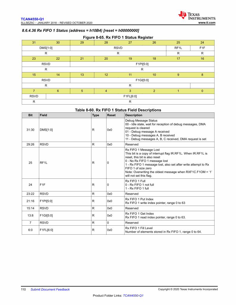
8.6.4.36 Rx FIFO 1 Status (address = h10B4) [reset = h00000000]
Figure 8-65. Rx FIFO 1 Status Register31 30 29 28 27 26 25 24
DMS[1:0] RSVD RF1L F1F
R R R R
23 22 21 20 19 18 17 16
RSVD F1PI[5:0]
R R
15 14 13 12 11 10 9 8
RSVD F1GI[5:0]
R R
7 6 5 4 3 2 1 0
RSVD F1FL[6:0]
R R
Table 8-60. Rx FIFO 1 Status Field DescriptionsBit Field Type Reset Description
31:30 DMS[1:0] R 0x0
Debug Message Status00 - Idle state, wait for reception of debug messages, DMArequest is cleared01 - Debug message A received10 - Debug messages A, B received11 - Debug messages A, B, C received, DMA request is set
29:26 RSVD R 0x0 Reserved
25 RF1L R 0
Rx FIFO 1 Message LostThis bit is a copy of interrupt flag IR.RF1L. When IR.RF1L isreset, this bit is also reset0 - No Rx FIFO 1 message lost1 - Rx FIFO 1 message lost, also set after write attempt to RxFIFO 1 of size zeroNote: Overwriting the oldest message when RXF1C.F1OM = ‘1’will not set this flag.
24 F1F R 0Rx FIFO 1 Full0 - Rx FIFO 1 not full1 - Rx FIFO 1 full
23:22 RSVD R 0x0 Reserved
21:16 F1PI[5:0] R 0x0 Rx FIFO 1 Put IndexRx FIFO 1 write index pointer, range 0 to 63
15:14 RSVD R 0x0 Reserved
13:8 F1GI[5:0] R 0x0 Rx FIFO 1 Get IndexRx FIFO 1 read index pointer, range 0 to 63.
7 RSVD R 0 Reserved
6:0 F1FL[6:0] R 0x0 Rx FIFO 1 Fill LevelNumber of elements stored in Rx FIFO 1, range 0 to 64.
TCAN4550-Q1SLLSEZ5C – JANUARY 2018 – REVISED OCTOBER 2020 www.ti.com
110 Submit Document Feedback Copyright © 2020 Texas Instruments Incorporated
Product Folder Links: TCAN4550-Q1

8.6.4.37 Rx FIFO 1 Acknowledge (address = h10B8) [reset = h00000000]
Figure 8-66. Rx FIFO 1 Acknowledge Register31 30 29 28 27 26 25 24
RSVD
R
23 22 21 20 19 18 17 16
RSVD
R
15 14 13 12 11 10 9 8
RSVD
R
7 6 5 4 3 2 1 0
RSVD F1AI[5:0]
R R/W
Table 8-61. Rx FIFO 1 Acknowledge Field DescriptionsBit Field Type Reset Description
31:24 RSVD R 0x0 Reserved
23:16 RSVD R 0x0 Reserved
15:8 RSVD R 0x0 Reserved
7:6 RSVD R 0x0 Reserved
5:0 F1AI[5:0] R/W 0x0
Rx FIFO 1 Acknowledge IndexAfter the Host has read a message or a sequence of messagesfrom Rx FIFO 1 it has to write the buffer index of the lastelement read from Rx FIFO 1 to F1AI. This will set the Rx FIFO1 Get Index RXF1S.F1GI to F1AI + 1 and update the FIFO 1 FillLevel RXF1S.F1FL.
www.ti.comTCAN4550-Q1
SLLSEZ5C – JANUARY 2018 – REVISED OCTOBER 2020
Copyright © 2020 Texas Instruments Incorporated Submit Document Feedback 111
Product Folder Links: TCAN4550-Q1
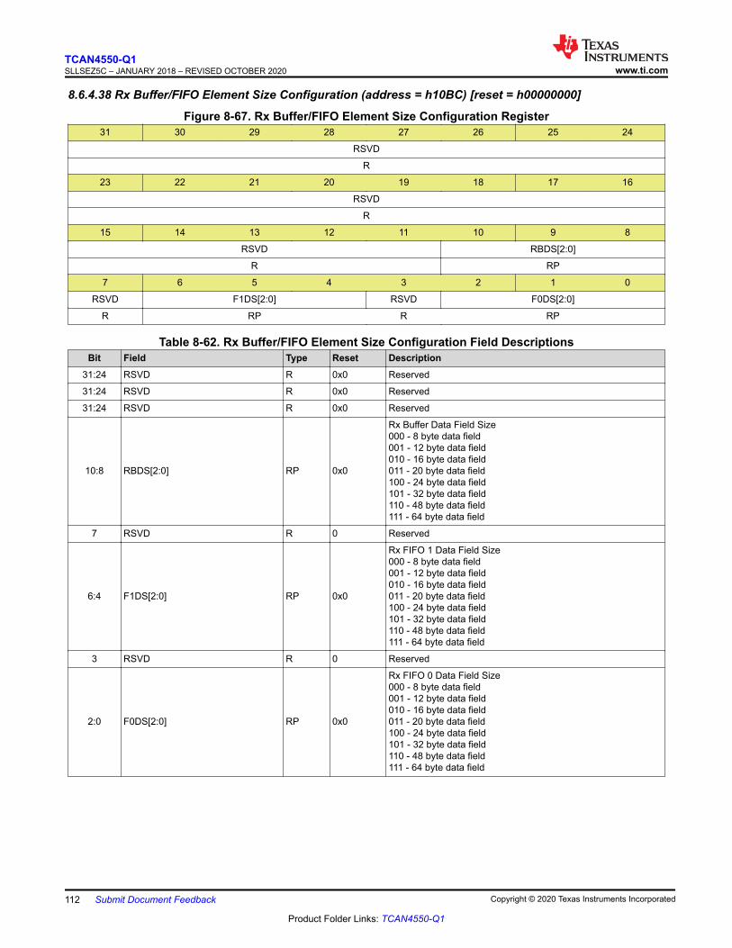
8.6.4.38 Rx Buffer/FIFO Element Size Configuration (address = h10BC) [reset = h00000000]
Figure 8-67. Rx Buffer/FIFO Element Size Configuration Register31 30 29 28 27 26 25 24
RSVD
R
23 22 21 20 19 18 17 16
RSVD
R
15 14 13 12 11 10 9 8
RSVD RBDS[2:0]
R RP
7 6 5 4 3 2 1 0
RSVD F1DS[2:0] RSVD F0DS[2:0]
R RP R RP
Table 8-62. Rx Buffer/FIFO Element Size Configuration Field DescriptionsBit Field Type Reset Description
31:24 RSVD R 0x0 Reserved
31:24 RSVD R 0x0 Reserved
31:24 RSVD R 0x0 Reserved
10:8 RBDS[2:0] RP 0x0
Rx Buffer Data Field Size000 - 8 byte data field001 - 12 byte data field010 - 16 byte data field011 - 20 byte data field100 - 24 byte data field101 - 32 byte data field110 - 48 byte data field111 - 64 byte data field
7 RSVD R 0 Reserved
6:4 F1DS[2:0] RP 0x0
Rx FIFO 1 Data Field Size000 - 8 byte data field001 - 12 byte data field010 - 16 byte data field011 - 20 byte data field100 - 24 byte data field101 - 32 byte data field110 - 48 byte data field111 - 64 byte data field
3 RSVD R 0 Reserved
2:0 F0DS[2:0] RP 0x0
Rx FIFO 0 Data Field Size000 - 8 byte data field001 - 12 byte data field010 - 16 byte data field011 - 20 byte data field100 - 24 byte data field101 - 32 byte data field110 - 48 byte data field111 - 64 byte data field
TCAN4550-Q1SLLSEZ5C – JANUARY 2018 – REVISED OCTOBER 2020 www.ti.com
112 Submit Document Feedback Copyright © 2020 Texas Instruments Incorporated
Product Folder Links: TCAN4550-Q1

8.6.4.39 Tx Buffer Configuration (address = h10C0) [reset = h00000000]
The MRAM and start address for this register, TBSA, has special consideration.• The start address must be word aligned (32-bit) in the MRAM. The 2 least significant bits are ignored on a
write to ensure this behavior.• When entering the MRAM start address, the 0x8000 prefix is NOT necessary. For example, if the desired
start address is 0x8634, then bits SA[15:0] will be 0x0634.
Figure 8-68. Tx Buffer Configuration Register31 30 29 28 27 26 25 24
RSVD TFQM TFQS[5:0]
R RP RP
23 22 21 20 19 18 17 16
RSVD NDTB[5:0]
R RP
15 14 13 12 11 10 9 8
TBSA[15:8]
RP
7 6 5 4 3 2 1 0
TBSA[7:0]
RP
Table 8-63. Tx Buffer Configuration Field DescriptionsBit Field Type Reset Description31 RSVD R 0 Reserved
30 TFQM RP 0Tx FIFO/Queue Mode0 - Tx FIFO operation1 - Tx Queue operation
29:24 TFQS[5:0] RP 0x0
Transmit FIFO/Queue Size0 - No Tx FIFO/Queue1-32 - Number of Tx Buffers used for Tx FIFO/Queue>32 - Values greater than 32 are interpreted as 32
23:22 RSVD R 0x0 Reserved
21:16 NDTB[5:0] RP 0x0
Number of Dedicated Transmit Buffers0 - No Dedicated Tx Buffers1-32 - Number of Dedicated Tx Buffers>32 - Values greater than 32 are interpreted as 32
15:0 TBSA[15:0] RP 0x0
Tx Buffers Start AddressStart address of Tx Buffers section in Message RAMNote: Be aware that the sum of TFQS and NDTB may be notgreater than 32. There is no check for erroneous configurations.The Tx Buffers section in the Message RAM starts with thededicated Tx Buffers.
www.ti.comTCAN4550-Q1
SLLSEZ5C – JANUARY 2018 – REVISED OCTOBER 2020
Copyright © 2020 Texas Instruments Incorporated Submit Document Feedback 113
Product Folder Links: TCAN4550-Q1

8.6.4.40 Tx FIFO/Queue Status (address = h10C4) [reset = h00000000]
Figure 8-69. Tx FIFO/Queue Status Register31 30 29 28 27 26 25 24
RSVD
R
23 22 21 20 19 18 17 16
RSVD TFQF TFQPI[4:0]
R R R
15 14 13 12 11 10 9 8
RSVD TFGI[4:0]
R R
7 6 5 4 3 2 1 0
RSVD TFFL[5:0]
R R
Table 8-64. Tx FIFO/Queue Status Field DescriptionsBit Field Type Reset Description
31:24 RSVD R 0x0 Reserved
23:22 RSVD R 0x0 Reserved
21 TFQF R 0Tx FIFO/Queue Full0 - Tx FIFO/Queue not full1 - Tx FIFO/Queue full
20:16 TFQPI[4:0] R 0x0 Tx FIFO/Queue Put IndexTx FIFO/Queue write index pointer, range 0 to 31.
15:13 RSVD R 0x0 Reserved
12:8 TFGI[4:0] R 0x0Tx FIFO Get IndexTx FIFO read index pointer, range 0 to 31. Read as zero whenTx Queue operation is configured (TXBC.TFQM = ‘1’).
7:6 RSVD R 0x0 Reserved
5:0 TFFL[5:0] R 0x0
Tx FIFO Free LevelNumber of consecutive free Tx FIFO elements starting fromTFGI, range 0 to 32. Read as zero when Tx Queue operation isconfigured (TXBC.TFQM = ‘1’)Note: In case of mixed configurations where dedicated TxBuffers are combined with a Tx FIFO or a Tx Queue, the Putand Get Indices indicate the number of the Tx Buffer startingwith the first dedicated Tx BuffersExample: For a configuration of 12 dedicated Tx Buffers and aTx FIFO of 20 Buffers a Put Index of 15 points to the fourthbuffer of the Tx FIFO
TCAN4550-Q1SLLSEZ5C – JANUARY 2018 – REVISED OCTOBER 2020 www.ti.com
114 Submit Document Feedback Copyright © 2020 Texas Instruments Incorporated
Product Folder Links: TCAN4550-Q1
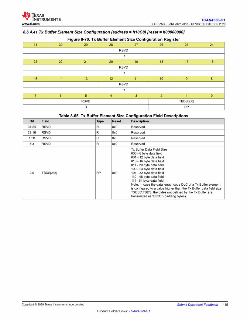
8.6.4.41 Tx Buffer Element Size Configuration (address = h10C8) [reset = h00000000]
Figure 8-70. Tx Buffer Element Size Configuration Register31 30 29 28 27 26 25 24
RSVD
R
23 22 21 20 19 18 17 16
RSVD
R
15 14 13 12 11 10 9 8
RSVD
R
7 6 5 4 3 2 1 0
RSVD TBDS[2:0]
R RP
Table 8-65. Tx Buffer Element Size Configuration Field DescriptionsBit Field Type Reset Description
31:24 RSVD R 0x0 Reserved
23:16 RSVD R 0x0 Reserved
15:8 RSVD R 0x0 Reserved
7:3 RSVD R 0x0 Reserved
2:0 TBDS[2:0] RP 0x0
Tx Buffer Data Field Size000 - 8 byte data field001 - 12 byte data field010 - 16 byte data field011 - 20 byte data field100 - 24 byte data field101 - 32 byte data field110 - 48 byte data field111 - 64 byte data fieldNote: In case the data length code DLC of a Tx Buffer elementis configured to a value higher than the Tx Buffer data field sizeTXESC.TBDS, the bytes not defined by the Tx Buffer aretransmitted as “0xCC” (padding bytes).
www.ti.comTCAN4550-Q1
SLLSEZ5C – JANUARY 2018 – REVISED OCTOBER 2020
Copyright © 2020 Texas Instruments Incorporated Submit Document Feedback 115
Product Folder Links: TCAN4550-Q1

8.6.4.42 Tx Buffer Request Pending (address = h10CC) [reset = h00000000]
Figure 8-71. Tx Buffer Request Pending Register31 30 29 28 27 26 25 24
TRP31 TRP30 TRP29 TRP28 TRP27 TRP26 TRP22 TRP24
R R R R R R R R
23 22 21 20 19 18 17 16
TRP23 TRP22 TRP21 TRP20 TRP19 TRP18 TRP17 TRP16
R R R R R R R R
15 14 13 12 11 10 9 8
TRP15 TRP14 TRP13 TRP12 TRP11 TRP10 TRP9 TRP8
R R R R R R R R
7 6 5 4 3 2 1 0
TRP7 TRP6 TRP5 TRP4 TRP3 TRP2 TRP1 TRP0
R R R R R R R R
Table 8-66. Tx Buffer Request Pending Field DescriptionsBit Field Type Reset Description
31:0 TRP31 to TRP0 R 0
Transmission Request PendingEach Tx Buffer has its own Transmission Request Pending bit.The bits are set via register TXBAR.The bits are reset after a requested transmission has completedor has been cancelled via register TXBCR. TXBRP bits are setonly for those Tx Buffers configured via TXBC. After a TXBRPbit has been set, a Tx scan is started to check for the pendingTx request with the highest priority (Tx Buffer with lowestMessage ID).A cancellation request resets the corresponding transmissionrequest pending bit of register TXBRP. In case a transmissionhas already been started when a cancellation is requested, thisis done at the end of the transmission, regardless whether thetransmission was successful or not. The cancellation requestbits are reset directly after the corresponding TXBRP bit hasbeen reset.After a cancellation has been requested, a finished cancellationis signaled via TXBCF• after successful transmission together with the
corresponding TXBTO bit• when the transmission has not yet been started at the point
of cancellation• when the transmission has been aborted due to lost
arbitration• when an error occurred during frame transmission
In DAR mode all transmissions are automatically cancelled ifthey are not successful. The corresponding TXBCF bit is set forall unsuccessful transmissions.0 - No transmission request pending1- Transmission request pendingNote: TXBRP bits which are set while a Tx scan is in progressare not considered during this particular Tx scan. In case acancellation is requested for such a Tx Buffer, this Add Requestis cancelled immediately, the corresponding TXBRP bit is reset.
TCAN4550-Q1SLLSEZ5C – JANUARY 2018 – REVISED OCTOBER 2020 www.ti.com
116 Submit Document Feedback Copyright © 2020 Texas Instruments Incorporated
Product Folder Links: TCAN4550-Q1

8.6.4.43 Tx Buffer Add Request (address = h10D0) [reset = h00000000]
Figure 8-72. Tx Buffer Add Request Register31 30 29 28 27 26 25 24
AR31 AR30 AR29 AR28 AR27 AR26 AR25 AR24
R/W R/W R/W R/W R/W R/W R/W R/W
23 22 21 20 19 18 17 16
AR23 AR22 AR21 AR20 AR19 AR18 AR17 AR16
R/W R/W R/W R/W R/W R/W R/W R/W
15 14 13 12 11 10 9 8
AR14 AR14 AR13 AR12 AR11 AR10 AR9 AR8
R/W R/W R/W R/W R/W R/W R/W R/W
7 6 5 4 3 2 1 0
AR7 AR6 AR5 AR4 AR3 AR2 AR1 AR0
R/W R/W R/W R/W R/W R/W R/W R/W
Table 8-67. Tx Buffer Add Request Field DescriptionsBit Field Type Reset Description
31:0 AR31 to AR0 R/W 0
Add RequestEach Tx Buffer has its own Add Request bit. Writing a ‘1’ will setthe corresponding Add Request bit; writing a ‘0’ has no impact.This enables the Host to set transmission requests for multipleTx Buffers with one write to TXBAR. TXBAR bits are set only forthose Tx Buffers configured via TXBC. When no Tx scan isrunning, the bits are reset immediately, else the bits remain setuntil the Tx scan process has completed.0 - No transmission request added1 - Transmission requested addedNote: If an add request is applied for a Tx Buffer with pendingtransmission request (corresponding TXBRP bit already set),this add request is ignored.
www.ti.comTCAN4550-Q1
SLLSEZ5C – JANUARY 2018 – REVISED OCTOBER 2020
Copyright © 2020 Texas Instruments Incorporated Submit Document Feedback 117
Product Folder Links: TCAN4550-Q1

8.6.4.43.1 Tx Buffer Cancellation Request (address = h10D4 [reset = h00000000]
Figure 8-73. Tx Buffer Cancellation Request Register31 30 29 28 27 26 25 24
CR31 CR30 CR29 CR28 CR27 CR26 CR25 CR24
R/W R/W R/W R/W R/W R/W R/W R/W
23 22 21 20 19 18 17 16
CR23 CR22 CR21 CR20 CR19 CR18 CR17 CR16
R/W R/W R/W R/W R/W R/W R/W R/W
15 14 13 12 11 10 9 8
CR15 CR14 CR13 CR12 CR11 CR10 CR9 CR8
R/W R/W R/W R/W R/W R/W R/W R/W
7 6 5 4 3 2 1 0
CR7 CR6 CR5 CR4 CR3 CR2 CR1 CR0
R/W R/W R/W R/W R/W R/W R/W R/W
Table 8-68. Tx Buffer Cancellation Request Field DescriptionsBit Field Type Reset Description
31:0 CR31 to CR0 R/W 0
Cancellation RequestEach Tx Buffer has its own Cancellation Request bit. Writing a‘1’ will set the corresponding Cancellation Request bit; writing a‘0’ has no impact. This enables the Host to set cancellationrequests for multiple Tx Buffers with one write to TXBCR.TXBCR bits are set only for those Tx Buffers configured viaTXBC. The bits remain set until the corresponding bit of TXBRPis reset.0 - No cancellation pending1 - Cancellation pending
TCAN4550-Q1SLLSEZ5C – JANUARY 2018 – REVISED OCTOBER 2020 www.ti.com
118 Submit Document Feedback Copyright © 2020 Texas Instruments Incorporated
Product Folder Links: TCAN4550-Q1

8.6.4.43.2 Tx Buffer Add Request Transmission Occurred (address = h10D8) [reset = h00000000]
Figure 8-74. Tx Buffer Add Request Transmission Occurred Register31 30 29 28 27 26 25 24
TO31 TO30 TO29 TO28 TO27 TO26 TO25 TO24
R R R R R R R R
23 22 21 20 19 18 17 16
TO23 TO22 TO21 TO20 TO19 TO18 TO17 TO16
R R R R R R R R
15 14 13 12 11 10 9 8
TO15 TO14 TO13 TO12 TO11 TO10 TO9 TO8
R R R R R R R R
7 6 5 4 3 2 1 0
TO7 TO6 TO5 TO4 TO3 TO2 TO1 TO0
R R R R R R R R
Table 8-69. Tx Buffer Add Request Transmission Occurred Field DescriptionsBit Field Type Reset Description
31:0 TO31 to TO0 R 0
Transmission OccurredEach Tx Buffer has its own Transmission Occurred bit. The bitsare set when the corresponding TXBRP bit is cleared after asuccessful transmission. The bits are reset when a newtransmission is requested by writing a ‘1’ to the correspondingbit of register TXBAR.0 - No transmission occurred1 - Transmission occurred
www.ti.comTCAN4550-Q1
SLLSEZ5C – JANUARY 2018 – REVISED OCTOBER 2020
Copyright © 2020 Texas Instruments Incorporated Submit Document Feedback 119
Product Folder Links: TCAN4550-Q1

8.6.4.43.3 Tx Buffer Cancellation Finished (address = h10DC) [reset = h00000000]
Figure 8-75. Tx Buffer Cancellation Finished Register31 30 29 28 27 26 25 24
CF31 CF30 CF29 CF28 CF27 CF26 CF25 CF24
R R R R R R R R
23 22 21 20 19 18 17 16
CF23 CF22 CF21 CF20 CF19 CF18 CF17 CF16
R R R R R R R R
15 14 13 12 11 10 9 8
CF15 CF14 CF13 CF12 CF11 CF10 CF9 CF8
R R R R R R R R
7 6 5 4 3 2 1 0
CF7 CF6 CF5 CF4 CF3 CF2 CF1 CF0
R R R R R R R R
Table 8-70. Tx Buffer Cancellation Finished Field DescriptionsBit Field Type Reset Description
31:0 CF31 to CF0 R 0
Cancellation FinishedEach Tx Buffer has its own Cancellation Finished bit. The bitsare set when the corresponding TXBRP bit is cleared after acancellation was requested via TXBCR. In case thecorresponding TXBRP bit was not set at the point ofcancellation, CF is set immediately. The bits are reset when anew transmission is requested by writing a ‘1’ to thecorresponding bit of register TXBAR.0 - No transmit buffer cancellation1 - Transmit buffer cancellation finished
TCAN4550-Q1SLLSEZ5C – JANUARY 2018 – REVISED OCTOBER 2020 www.ti.com
120 Submit Document Feedback Copyright © 2020 Texas Instruments Incorporated
Product Folder Links: TCAN4550-Q1

8.6.4.43.4 Tx Buffer Transmission Interrupt Enable (address = h10E0) [reset = h00000000]
Figure 8-76. Tx Buffer Transmission Interrupt Enable Register31 30 29 28 27 26 25 24
TIE31 TIE30 TIE29 TIE28 TIE27 TIE26 TIE25 TIE24
R/W R/W R/W R/W R/W R/W R/W R/W
23 22 21 20 19 18 17 16
TIE23 TIE22 TIE21 TIE20 TIE19 TIE18 TIE17 TIE16
R/W R/W R/W R/W R/W R/W R/W R/W
15 14 13 12 11 10 9 8
TIE15 TIE14 TIE13 TIE12 TIE11 TIE10 TIE9 TIE8
R/W R/W R/W R/W R/W R/W R/W R/W
7 6 5 4 3 2 1 0
TIE7 TIE6 TIE5 TIE4 TIE3 TIE2 TIE1 TIE0
R/W R/W R/W R/W R/W R/W R/W R/W
Table 8-71. Tx Buffer Transmission Interrupt Enable Field DescriptionsBit Field Type Reset Description
TIE31 to TIE0 R/W 0
Transmission Interrupt EnableEach Tx Buffer has its own Transmission Interrupt Enable bit.0 - Transmission interrupt disabled1 - Transmission interrupt enable
www.ti.comTCAN4550-Q1
SLLSEZ5C – JANUARY 2018 – REVISED OCTOBER 2020
Copyright © 2020 Texas Instruments Incorporated Submit Document Feedback 121
Product Folder Links: TCAN4550-Q1

8.6.4.43.5 Tx Buffer Cancellation Finished Interrupt Enable (address = h10E4) [reset = h00000000]
Figure 8-77. Tx Buffer Cancellation Finished Interrupt Enable Register31 30 29 28 27 26 25 24
CFIE31 CFIE30 CFIE29 CFIE28 CFIE27 CFIE26 CFIE25 CFIE24
R/W R/W R/W R/W R/W R/W R/W R/W
23 22 21 20 19 18 17 16
CFIE23 CFIE22 CFIE21 CFIE20 CFIE19 CFIE18 CFIE17 CFIE16
R/W R/W R/W R/W R/W R/W R/W R/W
15 14 13 12 11 10 9 8
CFIE15 CFIE14 CFIE13 CFIE12 CFIE11 CFIE10 CFIE9 CFIE8
R/W R/W R/W R/W R/W R/W R/W R/W
7 6 5 4 3 2 1 0
CFIE7 CFIE6 CFIE5 CFIE4 CFIE3 CFIE2 CFIE1 CFIE0
R/W R/W R/W R/W R/W R/W R/W R/W
Table 8-72. Tx Buffer Cancellation Finished Interrupt Enable Field DescriptionsBit Field Type Reset Description
31:0 CFIE31 to CFIE0 RW 0
Bit 31:0 CFIE[31:0]: Cancellation Finished Interrupt EnableEach Tx Buffer has its own Cancellation Finished InterruptEnable bit.0 - Cancellation finished interrupt disabled1 - Cancellation finished interrupt enabled
TCAN4550-Q1SLLSEZ5C – JANUARY 2018 – REVISED OCTOBER 2020 www.ti.com
122 Submit Document Feedback Copyright © 2020 Texas Instruments Incorporated
Product Folder Links: TCAN4550-Q1

8.6.4.43.6 Reserved (address = h10E8) [reset = h00000000]
Figure 8-78. Reserved31 30 29 28 27 26 25 24
RSVD
R
23 22 21 20 19 18 17 16
RSVD
R
15 14 13 12 11 10 9 8
RSVD
R
7 6 5 4 3 2 1 0
RSVD
R
Table 8-73. Reserved Field DescriptionsBit Field Type Reset Description
31:0 RSVD R 0 Reserved
www.ti.comTCAN4550-Q1
SLLSEZ5C – JANUARY 2018 – REVISED OCTOBER 2020
Copyright © 2020 Texas Instruments Incorporated Submit Document Feedback 123
Product Folder Links: TCAN4550-Q1

8.6.4.43.7 Reserved (address = h10EC) [reset = h00000000]
Figure 8-79. Reserved31 30 29 28 27 26 25 24
RSVD
R
23 22 21 20 19 18 17 16
RSVD
R
15 14 13 12 11 10 9 8
RSVD
R
7 6 5 4 3 2 1 0
RSVD
R
Table 8-74. Reserved Field DescriptionsBit Field Type Reset Description
31:0 RSVD R 0 Reserved
TCAN4550-Q1SLLSEZ5C – JANUARY 2018 – REVISED OCTOBER 2020 www.ti.com
124 Submit Document Feedback Copyright © 2020 Texas Instruments Incorporated
Product Folder Links: TCAN4550-Q1

8.6.4.43.8 Tx Event FIFO Configuration (address = h10F0) [reset = h00000000]
The MRAM and start address for this register, EFSA, has special consideration.• The start address must be word aligned (32-bit) in the MRAM. The 2 least significant bits are ignored on a
write to ensure this behavior.• When entering the MRAM start address, the 0x8000 prefix is NOT necessary. For example, if the desired
start address is 0x8634, then bits SA[15:0] will be 0x0634.
Figure 8-80. Tx Event FIFO Configuration Register31 30 29 28 27 26 25 24
RSVD EFWM[5:0]
R RP
23 22 21 20 19 18 17 16
RSVD EFS[5:0]
R RP
15 14 13 12 11 10 9 8
EFSA[15:8]
RP
7 6 5 4 3 2 1 0
EFSA[7:0]
RP
Table 8-75. Tx Event FIFO Configuration Field DescriptionsBit Field Type Reset Description
31:30 RSVD R 0x0 Reserved
29:24 EFWM[5:0] RP 0x0
Event FIFO Watermark0 - Watermark interrupt disabled1-32 - Level for Tx Event FIFO watermark interrupt (IR.TEFW)>32 - Watermark interrupt disabled
23:22 RSVD R 0x0 Reserved
21:16 EFS[5:0] RP 0x0
Event FIFO Size0 - Tx Event FIFO disabled1-32 - Number of Tx Event FIFO elements>32 - Values greater than 32 are interpreted as 32The Tx Event FIFO elements are indexed from 0 to EFS - 1
15:0 EFSA[15:0] RP 0x0 Event FIFO Start AddressStart address of Tx Event FIFO in Message RAM
www.ti.comTCAN4550-Q1
SLLSEZ5C – JANUARY 2018 – REVISED OCTOBER 2020
Copyright © 2020 Texas Instruments Incorporated Submit Document Feedback 125
Product Folder Links: TCAN4550-Q1

8.6.4.43.9 Tx Event FIFO Status (address = h10F4) [reset = h00000000]
Figure 8-81. Tx Event FIFO Status Register31 30 29 28 27 26 25 24
RSVD TEFL EFF
R R R
23 22 21 20 19 18 17 16
RSVD EFPI[4:0]
R R
15 14 13 12 11 10 9 8
RSVD REFGI[4:0]
R R
7 6 5 4 3 2 1 0
RSVD EFFL[5:0]
R R
Table 8-76. Tx Event FIFO Status Field DescriptionsBit Field Type Reset Description
31:26 RSVD R 0x0 Reserved
25 TEFL R 0
Tx Event FIFO Element LostThis bit is a copy of interrupt flag IR.TEFL. When IR.TEFL isreset, this bit is also reset.0 - No Tx Event FIFO element lost1 - Tx Event FIFO element lost, also set after write attempt to TxEvent FIFO of size zero.
24 EFF R 0Event FIFO Full0 - Tx Event FIFO not full1 - Tx Event FIFO full
23:21 RSVD R 0x0 Reserved
20:16 EFPI[4:0] R 0x0 Event FIFO Put IndexTx Event FIFO write index pointer, range 0 to 31.
15:13 RSVD R 0x0 Reserved
12:8 REFGI[4:0] R 0x0 Event FIFO Get IndexTx Event FIFO read index pointer, range 0 to 31.
7:6 RSVD R 0x0 Reserved
5:0 EFFL[5:0] R 0x0 Event FIFO Fill LevelNumber of elements stored in Tx Event FIFO, range 0 to 32
TCAN4550-Q1SLLSEZ5C – JANUARY 2018 – REVISED OCTOBER 2020 www.ti.com
126 Submit Document Feedback Copyright © 2020 Texas Instruments Incorporated
Product Folder Links: TCAN4550-Q1

8.6.4.43.10 Tx Event FIFO Acknowledge (address = h10F8) [reset = h00000000]
Figure 8-82. Tx Event FIFO Acknowledge Register31 30 29 28 27 26 25 24
RSVD
R23 22 21 20 19 18 17 16
RSVD
R15 14 13 12 11 10 9 8
RSVD
R7 6 5 4 3 2 1 0
RSVD EFAI[4:0]
R R/W
Table 8-77. Tx Event FIFO Acknowledge Field DescriptionsBit Field Type Reset Description
31:24 RSVD R 0x0 Reserved
23:16 RSVD R 0x0 Reserved
15:18 RSVD R 0x0 Reserved
7:5 RSVD R 0x0 Reserved
4:0 EFAI[4:0] E/W 0x0
Event FIFO Acknowledge IndexAfter the Host has read an element or a sequence of elementsfrom the Tx Event FIFO it has to write the index of the lastelement read from Tx Event FIFO to EFAI. This will set the TxEvent FIFO Get Index TXEFS.EFGI to EFAI + 1 and update theEvent FIFO Fill Level TXEFS.EFFL.
www.ti.comTCAN4550-Q1
SLLSEZ5C – JANUARY 2018 – REVISED OCTOBER 2020
Copyright © 2020 Texas Instruments Incorporated Submit Document Feedback 127
Product Folder Links: TCAN4550-Q1

8.6.4.43.11 Reserved (address = h10FC) [reset = h00000000]
Figure 8-83. Reserved31 30 29 28 27 26 25 24
RSVD
R
23 22 21 20 19 18 17 16
RSVD
R
15 14 13 12 11 10 9 8
RSVD
R
7 6 5 4 3 2 1 0
RSVD
R
Table 8-78. Reserved Field DescriptionsBit Field Type Reset Description
31:0 RSVD R 0 Reserved
TCAN4550-Q1SLLSEZ5C – JANUARY 2018 – REVISED OCTOBER 2020 www.ti.com
128 Submit Document Feedback Copyright © 2020 Texas Instruments Incorporated
Product Folder Links: TCAN4550-Q1

9 Application and ImplementationNote
Information in the following applications sections is not part of the TI component specification, and TIdoes not warrant its accuracy or completeness. TI’s customers are responsible for determiningsuitability of components for their purposes. Customers should validate and test their designimplementation to confirm system functionality.
9.1 Application Design Consideration9.1.1 Crystal and Clock Input Requirements
Selecting the crystal or clock input depends upon system implementation. To support 2 and 5 Mbps CAN FD theclock in or crystal needs to have 0.5% frequency accuracy. The minimum value of 20 MHz is needed to supportCAN FD with a rate of 2 Mbps. The recommended value for CLKIN or crystal is 40 MHz to meet CAN FD ratesup to 5 Mbps data rates in order to support higher data throughout. If a crystal is used see the manufacturer’sdocumentation on proper biasing.
Note
The TCAN4550-Q1 was evaluated with the NX2016SA 20MHz and 40MHz crystals
9.1.2 Bus Loading, Length and Number of Nodes
A typical CAN application can have a maximum bus length of 40 m and maximum stub length of 0.3 m. However,with careful design, users can have longer cables, longer stub lengths, and many more nodes to a bus. A highnumber of nodes require a transceiver with high input impedance such as this transceiver family.
Many CAN organizations and standards have scaled the use of CAN for applications outside the original ISO11898-2:2016 standard. They made system level trade off decisions for data rate, cable length, and parasiticloading of the bus. Examples of these CAN systems level specifications are ARINC825, CANopen, DeviceNet,SAE J2284, SAE J1939, and NMEA200.
A CAN system design is a series of tradeoffs. In ISO 11898-2:2016 the driver differential output is specified witha bus load that can range from 50 Ω to 65 Ω where the differential output must be greater than 1.5 V. TheTCAN4550-Q1 is specified to meet the 1.5 V requirement with a across this load range and is specified to meet1.4 V differential output at 45 Ω bus load. The differential input resistance of this family of transceiver is aminimum of 30kΩ. If 167 of these transceivers are in parallel on a bus, this is equivalent to an 180 Ω differentialload in parallel with the 60 Ω from termination gives a total bus load of 45 Ω. Therefore, this family theoreticallysupports over 167 transceivers on a single bus segment with margin to the 1.2 V minimum differential inputvoltage requirement at each receiving node. However for CAN network design margin must be given for signalloss across the system and cabling, parasitic loadings, timing, network imbalances, ground offsets and signalintegrity thus a practical maximum number of nodes is much lower. Bus length may also be extended beyond theoriginal ISO 11898-2:2016 standard of 40 m by careful system design and data rate tradeoffs. For exampleCANopen network design guidelines allow the network to be up to 1km with changes in the terminationresistance, cabling, less than 64 nodes and significantly lowered data rate.
This flexibility in CAN network design is one of its key strengths allowing for these system level networkextensions and additional standards to build on the original ISO 11898-2 CAN standard. However, when usingthis flexibility the CAN network system designer must take the responsibility of good network design to ensurerobust network operation.
9.1.3 CAN Termination
The standard CAN bus interconnection to be a single twisted pair cable (shielded or unshielded) with 120 Ωcharacteristic impedance (ZO).
www.ti.comTCAN4550-Q1
SLLSEZ5C – JANUARY 2018 – REVISED OCTOBER 2020
Copyright © 2020 Texas Instruments Incorporated Submit Document Feedback 129
Product Folder Links: TCAN4550-Q1

9.1.3.1 Termination
Resistors equal to the characteristic impedance of the line should be used to terminate both ends of the cable toprevent signal reflections. Unterminated drop-lines (stubs) connecting nodes to the bus should be kept as shortas possible to minimize signal reflections. The termination may be in a node but is generally not recommended,especially if the node may be removed from the bus. Termination must be carefully placed so that it is notremoved from the bus. System level CAN implementations such as CANopen allow for different termination andcabling concepts for example to add cable length.
MCU or DSP
TCAN4550
Node 1 MCU or DSP
CAN
Controller
TCAN1051/G
Node 2
MCU or DSP
CAN
Controller
Node 3
MCU or DSP
Node n
(with termination)
RTERM
TCAN1042/G
RTERM
TCAN4550
Figure 9-1. Typical CAN Bus
Termination may be a single 120 Ω resistor at each end of the bus, either on the cable or in a terminating node. Iffiltering and stabilization of the common mode voltage of the bus is desired then “split termination” may be used,see Figure 9-2. Split termination improves the electromagnetic emissions behavior of the network by eliminatingfluctuations in the bus common mode voltage levels at the start and end of message transmissions.
CAN
Transceiver
CAN
Transceiver
CANL
CANH
RTERM
CANL
CANH
RTERM/2
RTERM/2
CSPLIT
Standard Termination Split Termination
Figure 9-2. CAN Bus Termination Concepts
9.1.3.2 CAN Bus Biasing
Bus biasing can be normal biasing, active in normal mode and inactive in low-power mode. Automatic voltagebiasing is where the bus is active in normal mode but is controlled by the voltage between CANH and CANL inlower power modes. See Figure Figure 9-3 for the state diagram on how the TCAN4550-Q1 performs automaticbiasing. Figure Figure 9-4 provides the bus biasing based upon the mode of operation.
TCAN4550-Q1SLLSEZ5C – JANUARY 2018 – REVISED OCTOBER 2020 www.ti.com
130 Submit Document Feedback Copyright © 2020 Texas Instruments Incorporated
Product Folder Links: TCAN4550-Q1

Power On
Recessive state > tWK-FILTER
Dominant state > tWK-FILTER
Recessive state > tWK-FILTER
tWK_TIMEOUT
tWK_TIMEOUT
From all other nodes
Dominant state > tWK-FILTER
tSILENCE expired and implementation
In low power mode
tSILENCE expired and implementation
In low power mode
Low Power Mode:
Recessive state > tWK-FILTER
Normal Mode: Recessive state
Low Power Mode:
Dominant state > tWK-FILTER
Normal Mode: Dominant state
On implementation
enters Normal Mode
Bus Biasing Inactive
1
Bus Biasing Inactive
2
Bus Biasing Inactive
3
Bus Biasing Active
4
Bus Biasing
Active
Wait
Bus Biasing Inactive
Figure 9-3. Automatic bus biasing state diagram
www.ti.comTCAN4550-Q1
SLLSEZ5C – JANUARY 2018 – REVISED OCTOBER 2020
Copyright © 2020 Texas Instruments Incorporated Submit Document Feedback 131
Product Folder Links: TCAN4550-Q1

Power Up &
Reset
Standby Mode
Bus Bias: GND
Sleep Mode
Bus Bias: GND
Normal Mode
Bus Bias: 2.5 V
WAKE Pin
WUP
Prog to
Sleep Prog to
Normal
Standby Mode
Bus Bias: 2.5 V
Sleep Mode
Bus Bias: 2.5 V
Prog to
SleepProg to
Standby or
Fault
WUP
tSILENCEExpired
tSILENCEExpired
Yes
No No
Yes
tSILENCE
Expired
tSILENCE
Expired
WAKE
Pin
Fail-Safe
Figure 9-4. Bus Biasing Based on Modes of Operation
9.1.4 INH Brownout Behavior
A brownout condition takes place when VSUP ramps down below the minimum recommended operationconditions and then ramps back above the recommended operating conditions. Figure 9-5 provides the behaviorof the INH pin based upon process, voltage and temperature during this condition. Once VSUP drops below thedigital core going into reset, the device will have to be reprogrammed as all registers will be set back to default.
~ 4.7 V
~ 5.5 V UVSUP rise
UVSUP fallVSUP
INH
~ 3.6 VDigital core into reset
~ 4.25 VDigital core out
of reset
1.42 V < INH off < 3.14 V1.67 V > INH on > 4.15 V
Figure 9-5. INH Brownout Behavior
TCAN4550-Q1SLLSEZ5C – JANUARY 2018 – REVISED OCTOBER 2020 www.ti.com
132 Submit Document Feedback Copyright © 2020 Texas Instruments Incorporated
Product Folder Links: TCAN4550-Q1

9.2 Typical ApplicationThe TCAN4550-Q1 is typically used in applications with a host microprocessor or FPGA that does not includethe link layer portion of the CAN protocol. Below is a typical application configuration for 3.3 V microprocessorapplications.
SCLK
GPIO1
Reset
MCU
VCC
GPIOOptional:
TerminatingNode
Optional: Filtering,
Transient and ESD
Voltage Regulator
(e.g. TPSxxxx)
VIN
VOUT
VBAT
MOSI
MISO
nCS
VCCINT1
VLVRX for LP RX
2-wire CAN busSCLK
TX/RX CAN-FD Controller with
Filters
TX/RX Data Buffer
CANHTXD_INT
RXD_INT
LDO(s)
Under Voltage
POR
RST
VIO
WAKE
GND
Filter
VSUP
VINT
CNTL
VLVRX
VCCINT2
CANL
VIO
VIO
nCS
nINT
CAN-FD Transceiver
GPIO1
INH
EN
SPI slave, System
Controller
GPIO2GPO2
SDO
SDI
nWKRQGPIO3
VINT
VCCOUTFLTR
330 nF 10 µF
TCAN4550
OSC1 OSC2
40 MHz
CL
KO
UT
10 nF 33 k
3 k
10 µF
10 µF
100 nF
100 nF
Figure 9-6. Typical CAN Applications for TCAN4550-Q1 for 3.3 V µC and Crystal
Note: Add decoupling capacitors as needed.
www.ti.comTCAN4550-Q1
SLLSEZ5C – JANUARY 2018 – REVISED OCTOBER 2020
Copyright © 2020 Texas Instruments Incorporated Submit Document Feedback 133
Product Folder Links: TCAN4550-Q1

SCLK
GPIO1
Reset
MCU
VCC
GPIOOptional:
TerminatingNode
Optional: Filtering,
Transient and ESD
MOSI
MISO
nCS
VCCINT1
VLVRX for LP RX
2-wire CAN busSCLK
TX/RX CAN-FD Controller with
Filters
TX/RX Data Buffer
CANHTXD_INT
RXD_INT
LDO(s)
Under Voltage
POR
OSC1 OSC2
RST
VIO
GND
Filter
VINT
CNTL
VLVRX
VCCINT2
CANL
VIO
VIO
nCS
nINT
CAN-FD Transceiver
GPIO1
INH
SPI slave, System
Controller
GPIO2GPO2
SDO
SDI
nWKRQGPIO3
VINT
TCAN4550
OSC1 OSC2
20 MHz
CL
KO
UT
Voltage Regulator
(e.g. TPSxxxx)
VIN
VOUT
VBAT
WAKEVSUP
EN
VCCOUTFLTR
330 nF 10 µF
10 nF 33 k
3 k
10 µF
10 µF
100 nF
100 nF
Figure 9-7. Typical CAN Applications for TCAN4550-Q1 for 3.3 V µC; Clock from MCU
9.2.1 Detailed Requirements
The TCAN4550-Q1 works with 3.3 V and 5 V microprocessors when using the VIO pin from the microprocessorvoltage regulator. The bus termination is shown for illustrative purposes.
9.2.2 Detailed Design Procedures
The TCAN4550-Q1 is designed to work in application using the ISO 11898 standard supporting bus loads from50 Ω to 65 Ω. As the TCAN4550-Q1 supports CAN FD data rates up to 8 Mbps it is recommended to use a 40MHz crystal and keep trace lengths matched and short as feasible between the processor and device. As theCAN stub length are defined in the standard it is recommended to design the system according to these. As theTCAN4550-Q1 CAN transceiver is self-powered but also allows for up to 70 mA at 5 V to be sourced on VCCOUT,the system design needs to account for the CAN transceiver requirements when determining the load the LDO isto support. With this and the high temperature and input voltage range it is recommended to use a high-k boardusing proper thermal dissipation methods to ensure the highest performance.
9.2.3 Application Curves
Figure 9-8 and Figure 9-9 shows the behavior of the 5 V LDO in relationship to ISUP, VSUP, LDO load of 70 mA,CAN bus dominant and ambient temperature. The ISUP current is based upon a 70 mA load on VCCOUT and theCAN bus held dominant for about a total of 120 mA. As can be seen, an ambient temperature of 125°C cancause a thermal shut down event when VSUP reaches 20 V and VCCOUT is providing 70 mA to a load. The loadon the CAN bus is 60 Ω. When the CAN bus load is 50 Ω a VSUP of 19 V and ambient temperature of 125 cantrigger a thermal shut down event. The reason the curve shows ISUP leveling out to approximately 74.5 mA isdue to thermal shut down where the device shuts off the LDO and CAN transceiver. The device cools below TSDleaving thermal shutdown quickly. When the TSD event goes away the device then enters standby mode, turningon the LDO. The 74.5 mA is the 70 mA LDO load and a dominant on the CAN bus in standby mode. This ishappening quickly enough that LDO shut off is not seen. If the TSD event is prolonged the current would drop tomicro-amps and VCCOUT would be 0 V once the decoupling capacitor discharges.
TCAN4550-Q1SLLSEZ5C – JANUARY 2018 – REVISED OCTOBER 2020 www.ti.com
134 Submit Document Feedback Copyright © 2020 Texas Instruments Incorporated
Product Folder Links: TCAN4550-Q1

VSUP (V)
I SU
P (
mA
)
0 3 6 9 12 15 18 21 24 27 300
20
40
60
80
100
120
140
D003
-40°C25°C55°C85°C105°C125°C
A.VCCOUT = 5 V at 70mA
CAN Bus =Dominant
CAN Load = 60 Ω
Figure 9-8. ISUP vs VSUP CAN Dominant with 70 mALoad on VCCOUT
VSUP (V)
VC
CO
UT (
V)
0 3 6 9 12 15 18 21 24 27 300
0.5
1
1.5
2
2.5
3
3.5
4
4.5
5
5.5
D005
-40°C25°C55°C85°C105°C125°C
A.VCCOUT = 5 V at 70mA
CAN Bus =Dominant
CAN Load = 60 Ω
Figure 9-9. VCCOUT vs VSUP
www.ti.comTCAN4550-Q1
SLLSEZ5C – JANUARY 2018 – REVISED OCTOBER 2020
Copyright © 2020 Texas Instruments Incorporated Submit Document Feedback 135
Product Folder Links: TCAN4550-Q1

10 Power Supply RecommendationsThe TCAN4550-Q1 is designed to operate off of the battery Vbat. It has internal regulators to reduce the voltageto acceptable low power levels supporting the CAN FD controller, CAN transceiver and low voltage CANreceiver. In order to support a wide range of microprocessors the SPI and GPIO are powered off of the VIO pinwhich supports levels from 3 V to 5.5 V. Bulk capacitance, should be placed on the VSUP and the VIO voltagerails where system requirements are met. It is recommended that a capacitance of a 100 nF is placed near theTCAN4550-Q1 VSUP and the VIO supply terminals. The FLTR terminal requires a minimum of 300 nFcapacitance to ground to regulate the internal digital power rail. VCCOUT needs a minimum capacitance to groundof 10 µF at the terminal.
Note• The capacitance values selected should take into consideration the degradation over time such
that the values do not fall below the minimum values shown• Above is a minimum amount of capacitance but due to system considerations more may be
needed
TCAN4550-Q1SLLSEZ5C – JANUARY 2018 – REVISED OCTOBER 2020 www.ti.com
136 Submit Document Feedback Copyright © 2020 Texas Instruments Incorporated
Product Folder Links: TCAN4550-Q1

11 LayoutRobust and reliable bus node design often requires the use of external transient protection device in order toprotect against EFT and surge transients that may occur in industrial environments. Because ESD and transientshave a wide frequency bandwidth from approximately 3 MHz to 3 GHz, high-frequency layout techniques mustbe applied during PCB design. The family comes with high on-chip IEC ESD protection, but if higher levels ofsystem level immunity are desired external TVS diodes can be used. TVS diodes and bus filtering capacitorsshould be placed as close to the on-board connectors as possible to prevent noisy transient events frompropagating further into the PCB and system.
11.1 Layout GuidelinesPlace the protection and filtering circuitry as close to the bus connector, J1, to prevent transients, ESD and noisefrom propagating onto the board. The layout example provides information on components around the deviceitself. Transient voltage suppression (TVS) device can be added for extra protection, shown as D1. Theproduction solution can be either a bi-directional TVS diode or a varistor with ratings matching the applicationrequirements. This example also shows optional bus filter capacitors C10 and C11. A series common modechoke (CMC) is placed on the CANH and CANL lines between TCAN4550-Q1 and connector J1.
Design the bus protection components in the direction of the signal path. Do not force the transient current todivert from the signal path to reach the protection device. Use supply and ground planes to provide lowinductance.
Note
High-frequency currents follows the path of least impedance and not the path of least resistance.
Use at least two vias for supply and ground connections of bypass capacitors and protection devices to minimizetrace and via inductance.• Bypass and bulk capacitors should be placed as close as possible to the supply terminals of transceiver,
examples are C3, C4 and C5 on the FLTR, VIO, VCCOUT, pins and C6 and C7 on the VSUP supply.• Bus termination: this layout example shows split termination. This is where the termination is split into two
resistors, R5 and R6, with the center or split tap of the termination connected to ground via capacitor C9. Splittermination provides common mode filtering for the bus. When bus termination is placed on the board insteadof directly on the bus, additional care must be taken to ensure the terminating node is not removed from thebus thus also removing the termination.
• As terminal 8 (nINT) and 9 (GPO2) are open drain an external resistor to VIO is required. These can have avalue between 2 kΩ and 10 kΩ.
• Terminal 12 (WAKE) is a bi-directional triggered wake up input that is usually connected to an external switch.It should be configured as shown with a 10 nF (C8) to GND where R2 is 33 kΩ and R3 is 3 kΩ.
• Terminal 15 (INH) can be left floating if not used but a 100 kΩ pull-down resistor can be used to discharge theINH to a sufficient level when the INH output is high-Z.
www.ti.comTCAN4550-Q1
SLLSEZ5C – JANUARY 2018 – REVISED OCTOBER 2020
Copyright © 2020 Texas Instruments Incorporated Submit Document Feedback 137
Product Folder Links: TCAN4550-Q1

11.2 Layout Example
Choke
2
9
19
12
1 20
10
11
GND
GND
GND
GND
GND
VIO
VIO
VSUP
VSUP
VCCOUT
VIO
FLTR
RST
INH
WAKE
To Switch
GPO2
nINT
nCS
SDO
SDI
SCLK
GPIO1
nWKRQ
CANHCANL
GNDC1 C2
C3
C4
C5
C6 C7
C8
GND
C9
R1
R2
R3
R5 R4
R6
R7
GNDCrystal
40 MHz
50
Traces for Pin 1 and 20
need to be Matched length
C10C11
J1
D1
Figure 11-1. Example Layout
TCAN4550-Q1SLLSEZ5C – JANUARY 2018 – REVISED OCTOBER 2020 www.ti.com
138 Submit Document Feedback Copyright © 2020 Texas Instruments Incorporated
Product Folder Links: TCAN4550-Q1

12 Device and Documentation Support12.1 Documentation Support12.1.1 Related Documentation12.1.1.1 CAN Transceiver Physical Layer Standards:
• ISO 11898-2:2016: High speed medium access unit with low power mode• ISO 8802-3: CSMA/CD – referenced for collision detection from ISO11898-2• CAN FD 1.0 Spec and Papers• Bosch “Configuration of CAN Bit Timing”, Paper from 6th International CAN Conference (ICC), 1999. This is
repeated a lot in the DCAN IP CAN Controller spec copied into this system spec.• SAE J2284-2: High Speed CAN (HSC) for Vehicle Applications at 250 kbps• SAE J2284-3: High Speed CAN (HSC) for Vehicle Applications at 500 kbps• Bosch M_CAN Controller Area Network Revision 3.2.1.1 (3/24/2016)
12.1.1.2 EMC requirements:
• SAE J2962-2: US3 requirements for CAN Transceivers• HW Requirements for CAN, LIN,FR V1.3:
12.1.1.3 Conformance Test requirements:
• HS_TRX_Test_Spec_V_1_0: GIFT / ICT CAN test requirements for High Speed Physical Layer
12.1.1.4 Support Documents
• “A Comprehensible Guide to Controller Area Network”, Wilfried Voss, Copperhill Media Corporation• “CAN System Engineering: From Theory to Practical Applications”, 2nd Edition, 2013; Dr. Wolfhard Lawrenz,
Springer.
12.2 Receiving Notification of Documentation UpdatesTo receive notification of documentation updates, navigate to the device product folder on ti.com. Click onSubscribe to updates to register and receive a weekly digest of any product information that has changed. Forchange details, review the revision history included in any revised document.
12.3 Support ResourcesTI E2E™ support forums are an engineer's go-to source for fast, verified answers and design help — straightfrom the experts. Search existing answers or ask your own question to get the quick design help you need.
Linked content is provided "AS IS" by the respective contributors. They do not constitute TI specifications and donot necessarily reflect TI's views; see TI's Terms of Use.
12.4 TrademarksTI E2E™ is a trademark of Texas Instruments.All other trademarks are the property of their respective owners.12.5 Electrostatic Discharge Caution
This integrated circuit can be damaged by ESD. Texas Instruments recommends that all integrated circuits be handledwith appropriate precautions. Failure to observe proper handling and installation procedures can cause damage.ESD damage can range from subtle performance degradation to complete device failure. Precision integrated circuits maybe more susceptible to damage because very small parametric changes could cause the device not to meet its publishedspecifications.
12.6 GlossaryTI Glossary This glossary lists and explains terms, acronyms, and definitions.
www.ti.comTCAN4550-Q1
SLLSEZ5C – JANUARY 2018 – REVISED OCTOBER 2020
Copyright © 2020 Texas Instruments Incorporated Submit Document Feedback 139
Product Folder Links: TCAN4550-Q1

13 Mechanical, Packaging, and Orderable InformationThe following pages include mechanical, packaging, and orderable information. This information is the mostcurrent data available for the designated devices. This data is subject to change without notice and revision ofthis document. For browser-based versions of this data sheet, refer to the left-hand navigation.
TCAN4550-Q1SLLSEZ5C – JANUARY 2018 – REVISED OCTOBER 2020 www.ti.com
140 Submit Document Feedback Copyright © 2020 Texas Instruments Incorporated
Product Folder Links: TCAN4550-Q1
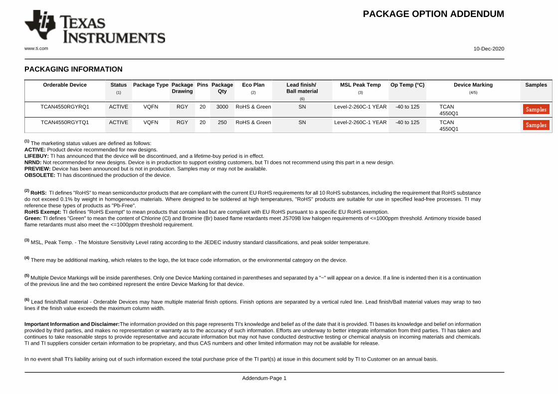
PACKAGE OPTION ADDENDUM
www.ti.com 10-Dec-2020
Addendum-Page 1
PACKAGING INFORMATION
Orderable Device Status(1)
Package Type PackageDrawing
Pins PackageQty
Eco Plan(2)
Lead finish/Ball material
(6)
MSL Peak Temp(3)
Op Temp (°C) Device Marking(4/5)
Samples
TCAN4550RGYRQ1 ACTIVE VQFN RGY 20 3000 RoHS & Green SN Level-2-260C-1 YEAR -40 to 125 TCAN4550Q1
TCAN4550RGYTQ1 ACTIVE VQFN RGY 20 250 RoHS & Green SN Level-2-260C-1 YEAR -40 to 125 TCAN4550Q1
(1) The marketing status values are defined as follows:ACTIVE: Product device recommended for new designs.LIFEBUY: TI has announced that the device will be discontinued, and a lifetime-buy period is in effect.NRND: Not recommended for new designs. Device is in production to support existing customers, but TI does not recommend using this part in a new design.PREVIEW: Device has been announced but is not in production. Samples may or may not be available.OBSOLETE: TI has discontinued the production of the device.
(2) RoHS: TI defines "RoHS" to mean semiconductor products that are compliant with the current EU RoHS requirements for all 10 RoHS substances, including the requirement that RoHS substancedo not exceed 0.1% by weight in homogeneous materials. Where designed to be soldered at high temperatures, "RoHS" products are suitable for use in specified lead-free processes. TI mayreference these types of products as "Pb-Free".RoHS Exempt: TI defines "RoHS Exempt" to mean products that contain lead but are compliant with EU RoHS pursuant to a specific EU RoHS exemption.Green: TI defines "Green" to mean the content of Chlorine (Cl) and Bromine (Br) based flame retardants meet JS709B low halogen requirements of <=1000ppm threshold. Antimony trioxide basedflame retardants must also meet the <=1000ppm threshold requirement.
(3) MSL, Peak Temp. - The Moisture Sensitivity Level rating according to the JEDEC industry standard classifications, and peak solder temperature.
(4) There may be additional marking, which relates to the logo, the lot trace code information, or the environmental category on the device.
(5) Multiple Device Markings will be inside parentheses. Only one Device Marking contained in parentheses and separated by a "~" will appear on a device. If a line is indented then it is a continuationof the previous line and the two combined represent the entire Device Marking for that device.
(6) Lead finish/Ball material - Orderable Devices may have multiple material finish options. Finish options are separated by a vertical ruled line. Lead finish/Ball material values may wrap to twolines if the finish value exceeds the maximum column width.
Important Information and Disclaimer:The information provided on this page represents TI's knowledge and belief as of the date that it is provided. TI bases its knowledge and belief on informationprovided by third parties, and makes no representation or warranty as to the accuracy of such information. Efforts are underway to better integrate information from third parties. TI has taken andcontinues to take reasonable steps to provide representative and accurate information but may not have conducted destructive testing or chemical analysis on incoming materials and chemicals.TI and TI suppliers consider certain information to be proprietary, and thus CAS numbers and other limited information may not be available for release.
In no event shall TI's liability arising out of such information exceed the total purchase price of the TI part(s) at issue in this document sold by TI to Customer on an annual basis.
PACKAGE OPTION ADDENDUM
www.ti.com 10-Dec-2020
Addendum-Page 2
OTHER QUALIFIED VERSIONS OF TCAN4550-Q1 :
• Catalog: TCAN4550
NOTE: Qualified Version Definitions:
• Catalog - TI's standard catalog product

TAPE AND REEL INFORMATION
*All dimensions are nominal
Device PackageType
PackageDrawing
Pins SPQ ReelDiameter
(mm)
ReelWidth
W1 (mm)
A0(mm)
B0(mm)
K0(mm)
P1(mm)
W(mm)
Pin1Quadrant
TCAN4550RGYRQ1 VQFN RGY 20 3000 330.0 12.4 3.8 4.8 1.18 8.0 12.0 Q1
TCAN4550RGYTQ1 VQFN RGY 20 250 180.0 12.4 3.8 4.8 1.18 8.0 12.0 Q1
PACKAGE MATERIALS INFORMATION
www.ti.com 8-Jan-2021
Pack Materials-Page 1
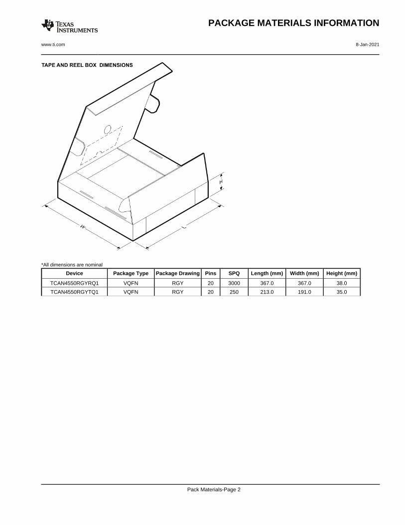
*All dimensions are nominal
Device Package Type Package Drawing Pins SPQ Length (mm) Width (mm) Height (mm)
TCAN4550RGYRQ1 VQFN RGY 20 3000 367.0 367.0 38.0
TCAN4550RGYTQ1 VQFN RGY 20 250 213.0 191.0 35.0
PACKAGE MATERIALS INFORMATION
www.ti.com 8-Jan-2021
Pack Materials-Page 2
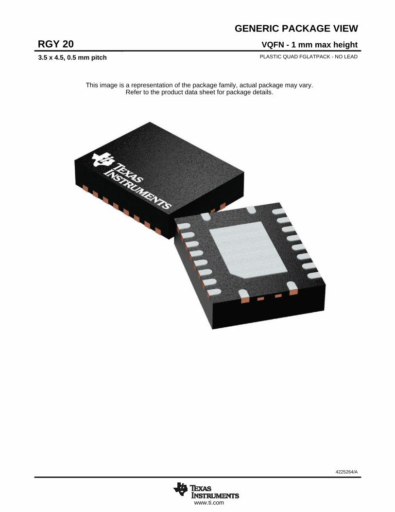
www.ti.com
GENERIC PACKAGE VIEW
This image is a representation of the package family, actual package may vary.Refer to the product data sheet for package details.
VQFN - 1 mm max heightRGY 20PLASTIC QUAD FGLATPACK - NO LEAD3.5 x 4.5, 0.5 mm pitch
4225264/A

A A
www.ti.com
PACKAGE OUTLINE
C
20X 0.30.2
2.2 0.1
20X 0.50.3
1 MAX
(0.2) TYP
0.050.00
14X 0.5
2X3.5
2X 1.5
3.2 0.1
4X 0.25 0.05
4.2 0.1
A 3.63.4
B
4.64.4
(0.05)
0.1 MIN
VQFN - 1 mm max heightRGY0020CPLASTIC QUAD FLATPACK - NO LEAD
4223814/A 06/2017
PIN 1 INDEX AREA
0.08 C
SEATING PLANE
1
912
10 11
2019
(OPTIONAL)PIN 1 ID
0.1 C A B0.05
EXPOSEDTHERMAL PAD
21SYMM
SYMM
2
NOTES: 1. All linear dimensions are in millimeters. Any dimensions in parenthesis are for reference only. Dimensioning and tolerancing per ASME Y14.5M. 2. This drawing is subject to change without notice. 3. The package thermal pad must be soldered to the printed circuit board for thermal and mechanical performance.
SCALE 3.000
SCALE 30.000SECTION A-ASECTION A-A
TYPICAL

www.ti.com
EXAMPLE BOARD LAYOUT
0.07 MINALL AROUND
0.07 MAXALL AROUND
20X (0.6)
20X (0.25)
14X (0.5)
(2.2)
(3.2)4X
(4.3)
4X (0.75)
(1.35)
(3.3)
(0.85)
(R0.05) TYP
2X (0.75)4X (0.25)
(4.2)
( 0.2) TYPVIA
VQFN - 1 mm max heightRGY0020CPLASTIC QUAD FLATPACK - NO LEAD
4223814/A 06/2017
SYMM1
9
10 11
12
219
20
SYMM
LAND PATTERN EXAMPLEEXPOSED METAL SHOWN
SCALE:18X
21
NOTES: (continued) 4. This package is designed to be soldered to a thermal pad on the board. For more information, see Texas Instruments literature number SLUA271 (www.ti.com/lit/slua271).5. Vias are optional depending on application, refer to device data sheet. If any vias are implemented, refer to their locations shown on this view. It is recommended that vias under paste be filled, plugged or tented.
SOLDER MASKOPENING
METAL UNDERSOLDER MASK
SOLDER MASKDEFINED
EXPOSED METALMETAL
SOLDER MASKOPENING
SOLDER MASK DETAILS
NON SOLDER MASKDEFINED
(PREFERRED)
EXPOSED METAL

www.ti.com
EXAMPLE STENCIL DESIGN
2X (0.25)
20X (0.6)
24X (0.25)
14X (0.5)
(3.3)
4X(4.3)
4X (0.98)
(0.82)TYP
4X (0.75)
(R0.05) TYP 4X(1.43)
(0.59) TYP
2X (0.2)
VQFN - 1 mm max heightRGY0020CPLASTIC QUAD FLATPACK - NO LEAD
4223814/A 06/2017
NOTES: (continued) 6. Laser cutting apertures with trapezoidal walls and rounded corners may offer better paste release. IPC-7525 may have alternate design recommendations.
SYMM
EXPOSED METALTYP
SOLDER PASTE EXAMPLEBASED ON 0.125 mm THICK STENCIL
EXPOSED PAD 21
80% PRINTED SOLDER COVERAGE BY AREA UNDER PACKAGESCALE:20X
SYMM21
1
9
10 11
12
219
20

IMPORTANT NOTICE AND DISCLAIMERTI PROVIDES TECHNICAL AND RELIABILITY DATA (INCLUDING DATASHEETS), DESIGN RESOURCES (INCLUDING REFERENCEDESIGNS), APPLICATION OR OTHER DESIGN ADVICE, WEB TOOLS, SAFETY INFORMATION, AND OTHER RESOURCES “AS IS”AND WITH ALL FAULTS, AND DISCLAIMS ALL WARRANTIES, EXPRESS AND IMPLIED, INCLUDING WITHOUT LIMITATION ANYIMPLIED WARRANTIES OF MERCHANTABILITY, FITNESS FOR A PARTICULAR PURPOSE OR NON-INFRINGEMENT OF THIRDPARTY INTELLECTUAL PROPERTY RIGHTS.These resources are intended for skilled developers designing with TI products. You are solely responsible for (1) selecting the appropriateTI products for your application, (2) designing, validating and testing your application, and (3) ensuring your application meets applicablestandards, and any other safety, security, or other requirements. These resources are subject to change without notice. TI grants youpermission to use these resources only for development of an application that uses the TI products described in the resource. Otherreproduction and display of these resources is prohibited. No license is granted to any other TI intellectual property right or to any third partyintellectual property right. TI disclaims responsibility for, and you will fully indemnify TI and its representatives against, any claims, damages,costs, losses, and liabilities arising out of your use of these resources.TI’s products are provided subject to TI’s Terms of Sale (https:www.ti.com/legal/termsofsale.html) or other applicable terms available eitheron ti.com or provided in conjunction with such TI products. TI’s provision of these resources does not expand or otherwise alter TI’sapplicable warranties or warranty disclaimers for TI products.IMPORTANT NOTICE
Mailing Address: Texas Instruments, Post Office Box 655303, Dallas, Texas 75265Copyright © 2021, Texas Instruments Incorporated