tb-fmcl-mipi hardware user manual - solutions.inrevium.com · tb-fmcl-mipi hardware user manual...
TRANSCRIPT

TB-FMCL-MIPI Hardware User Manual
1 Rev.3.01
TB-FMCL-MIPI Hardware User Manual
Rev.3.01

TB-FMCL-MIPI Hardware User Manual
2 Rev.3.01
Revision History
Version Date Description Publisher
Rev.1.00 5/22/2015 Initial release RH
Rev.1.10 5/25/2015 Reviewed and updated. General Release RH
Rev.1.99 8/26/2015 Reviewed. Updated for PA-10087-0x Rev2.0. Submitted for
review.
ST
Rev. 2.00 9/14/2015 Updated. Released. ST
Rev. 3.00 11/30/2015 Updated with new connector information ST
Rev. 3.01 6/30/2016 Updated 2.Overview , 8.2 HS Mode Interface
Updated Figure.4-1, Figure.7-1, Figure.10-1
Amano

TB-FMCL-MIPI Hardware User Manual
3 Rev.3.01
Table of Contents
1. Related Documents and Accessories .......................................................................................... 8
2. Overview ...................................................................................................................................... 8
3. Features ....................................................................................................................................... 9
4. Block Diagram ........................................................................................................................... 10
5. External View of the Board ........................................................................................................ 11
6. Board Specification .................................................................................................................... 13
7. Board Power System ................................................................................................................. 14
7.1. Power System Overview .......................................................................................................... 14
7.2. MIPI User Power Rail ............................................................................................................... 14
7.3. LDO regulators ......................................................................................................................... 15
7.4. LED Power Indicators ............................................................................................................... 15
8. MIPI PHY Device to FMC Interface ........................................................................................... 15
8.1. PHY Device Overview .............................................................................................................. 15
8.2. HS Mode Interface.................................................................................................................... 15
8.3. LP Mode Interface .................................................................................................................... 16
8.4. PHY Control .............................................................................................................................. 16
9. MIPI IO Signals .......................................................................................................................... 17
9.1. MIPI D-PHY Lanes ................................................................................................................... 17
9.2. MIPI GPIO Signals ................................................................................................................... 17
9.3. MIPI I2C Bus ............................................................................................................................ 19
10. Connectors ................................................................................................................................ 19
10.1. LPC FMC Connector to Host Carrier Board ......................................................................... 19
10.2. MIPI Front Edge (I/O Window) Receptacles ........................................................................ 24
10.3. MIPI GPIO and I2C Debug Headers .................................................................................... 26
11. FMC Facility I2C Bus ................................................................................................................. 27
11.1. FMC I2C EEPROM ............................................................................................................... 27
12. ESD Protection .......................................................................................................................... 27
13. Demonstration ........................................................................................................................... 27
14. Appendix A: FMC I2C EEPROM ............................................................................................... 28
15. Appendix B: Headers, Factory Default, and Orientation ........................................................... 31

TB-FMCL-MIPI Hardware User Manual
4 Rev.3.01
List of Figures
Figure 3-1 FMC LPC Connector Pinout per VITA 57.1 ...................................................................... 9
Figure 4-1 TB-FMCL-MIPI Block Diagram ....................................................................................... 10
Figure 5-1 Photo of TB-FMCL-MIPI (Side 1) .....................................................................................11
Figure 5-2 Photo of TB-FMCL-MIPI (Side 2) .................................................................................... 12
Figure 6-1 TB-FMCL-MIPI Board Dimensions (mm) ........................................................................ 13
Figure 7-1 TB-FMCL-MIPI Power Structure ..................................................................................... 14
Figure 7-2 VUSER Jumper Select Positions .................................................................................... 14
Figure 7-3 Power LEDs Identification ............................................................................................... 15
Figure 9-1 GPIO SIGNALS TO EACH MIPI PORT .......................................................................... 17
Figure 9-2 MIPI GPIO Voltage Select Options ................................................................................. 18
Figure 10-1 Resistor for connection to TB-7V-2000T-LSI ................................................................ 23
Figure 10-2 MIPI Connectors Faceplate View ................................................................................. 24
Figure 10-3 Axial removal vs zippering (picture courtesy of Samtec®) ............................................ 24
Figure 10-4 MIPI Debug header side access views ......................................................................... 26
Figure 15-1 Default Jumper Positions and Header Orientation ....................................................... 31
List of Tables
Table 1-1 Accessories ........................................................................................................................ 8
Table 8-1 MIPI PHY Mode Settings .................................................................................................. 16
Table 9-1 GPIO Signals: Recommended sequencing ...................................................................... 18
Table 10-1 LPC FMC Host Board Connector Pin Assignment ......................................................... 20
Table 10-2 MIPI D-PHY PORT A J5 (CSI) ........................................................................................ 25
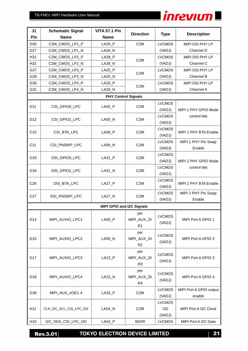
Table 10-3 MIPI D-PHY PORT B J16 (DSI) ..................................................................................... 26
Table 10-4 MIPI GPIO Debug Headers J15 and J18 ....................................................................... 27
Table 14-1 FMC I2C EEPROM Contents ......................................................................................... 28
Table 15-1 Default Header Explanation ........................................................................................... 31

TB-FMCL-MIPI Hardware User Manual
5 Rev.3.01
Introduction Thank you for purchasing the TB-FMCL-MIPI board. Before using the product, be sure to carefully
read this user manual and fully understand how to correctly use the product. First read through this
manual, and then always keep it handy.
SAFETY PRECAUTIONS Be sure to observe these precautions!
Observe the precautions listed below to prevent injuries to you or other personnel or damage to property.
Before using the product, read these safety precautions carefully to assure correct use.
These precautions contain serious safety instructions that must be observed.
After reading through this manual, be sure to always keep it handy.
The following conventions are used to indicate the possibility of injury/damage and classify precautions if
the product is handled incorrectly.
Indicates the high possibility of serious injury or death if the product is handled
incorrectly.
Indicates the possibility of serious injury or death if the product is handled
incorrectly.
Indicates the possibility of injury or physical damage in connection with houses or
household goods if the product is handled incorrectly.
The following graphical symbols are used to indicate and classify precautions in this manual.
(Examples)
Turn off the power switch.
Do not disassemble the product.
Do not attempt this.
Danger
Warning
Caution

TB-FMCL-MIPI Hardware User Manual
6 Rev.3.01
In the event of a failure, disconnect the power supply.
If the product is used as is, a fire or electric shock may occur. Disconnect the power supply
immediately and contact our sales personnel for repair.
If an unpleasant smell or smoking occurs, disconnect the power supply.
If the product is used as is, a fire or electric shock may occur. Disconnect the power supply
immediately. After verifying that there is no smoking, contact our sales personnel for repair.
Do not disassemble, repair or modify the product.
Otherwise, a fire or electric shock may occur due to a short circuit or heat generation. For
inspection, modification or repair, contact our sales personnel.
Do not touch a cooling fan.
As a cooling fan rotates at high speed, do not put your hand close to it. Otherwise, it may
cause injury to persons. Never touch a rotating cooling fan.
Do not place the product on unstable locations.
Otherwise, it may drop or fall, resulting in injury to persons or failure.
If the product is dropped or damaged, do not use it as is.
Otherwise, a fire or electric shock may occur.
Do not touch the product with a metallic object.
Otherwise, a fire or electric shock may occur.
Do not place the product in dusty or humid locations or where water may
splash.
Otherwise, a fire or electric shock may occur.
Do not get the product wet or touch it with a wet hand.
Otherwise, the product may break down or it may cause a fire, smoking or electric shock.
Do not touch a connector on the product (gold-plated portion).
Otherwise, the surface of a connector may be contaminated with sweat or skin oil, resulting
in contact failure of a connector or it may cause a malfunction, fire or electric shock due to
static electricity.
Warning

TB-FMCL-MIPI Hardware User Manual
7 Rev.3.01
Do not use or place the product in the following locations.
Humid and dusty locations
Airless locations such as closet or bookshelf
Locations which receive oily smoke or steam
Locations exposed to direct sunlight
Locations close to heating equipment
Closed inside of a car where the temperature becomes high
Static-prone locations
Locations close to water or chemicals
Otherwise, a fire, electric shock, accident or deformation may occur due to a short circuit or heat
generation.
Do not place heavy things on the product.
Otherwise, the product may be damaged.
■ Disclaimer
This product is a MIPI interface for Xilinx FPGA evaluation boards. Tokyo Electron Device Limited
assumes no responsibility for any damages resulting from the use of this product for purposes other than
those stated.
Even if the product is used properly, Tokyo Electron Device Limited assumes no responsibility for any
damages caused by:
(1) Earthquake, thunder, natural disaster or fire resulting from the use beyond our responsibility, acts by
a third party or other accidents, the customer’s willful or accidental misuse, or use under other
abnormal conditions.
(2) Secondary impact arising from use of this product or its unusable state (business interruption or
others)
(3) Use of this product against the instructions given in this manual.
(4) Malfunctions due to connection to other devices.
Tokyo Electron Device Limited assumes no responsibility or liability for:
(1) Erasure or corruption of data arising from use of this product.
(2) Any consequences or other abnormalities arising from use of this product, or
(3) Damage of this product not due to our responsibility or failure due to modification.
This product has been developed by assuming its use for research, testing or evaluation. It is not
authorized for use in any system or application that requires high reliability.
Repair of this product is carried out by replacing it on a chargeable basis, not repairing the faulty devices.
However, non-chargeable replacement is offered for initial failure if such notification is received within
two weeks after delivery of the product.
The specification of this product is subject to change without prior notice.
The product is subject to discontinuation without prior notice.
Caution

TB-FMCL-MIPI Hardware User Manual
8 Rev.3.01
1. Related Documents and Accessories
All documents relating to this board can be downloaded from the TED Support Web at address
https://www.teldevice.co.jp/spweb/c0201s
Table 1-1 Accessories
Description Manufacturer Quantity
Spacer, 10mm, M2.6 Hirosugi 2
Spacer, 25mm, M2.6 Hirosugi 2
Screw, 6mm, M2.6 w/ washers Hirosugi 6
2. Overview
The TB-FMCL-MIPI is an ANSI/VITA 57.1 compatible FPGA Mezzanine Card (FMC) with a
Low-Pin-Count (LPC) connector that presents two separate 4-lane MIPI ports to a pair of 40-pin
sockets located in the FMC I/O Window. Each side utilizes a PHY device designed to be
compatible with the MIPI D-PHY Specification 1.00.00, (September 2009) meeting the nominal
data throughput of 1 Gbit/s per lane.
The TB-FMCL-MIPI does not utilize any of the high-speed serial DPx data links and GBTCLKs
provided in the FMC standard, so present data speed is limited to the capabilities of HR and HP
SelectIO of Xilinx FPGAs.
The TB-FMCL-MIPI is produced as a CSI-DSI combo card that supports 4-lane MIPI input and
4-lane MIPI output on a single FMC LPC module.
Note: Through factory configuration (population options), the ports on the circuit board can support
CSI/DSI (default), CSI x2 (custom build required), or DSI x2 (custom build required). Please
contact a sales representative regarding custom board versions.
TB-FMCL-MIPI Hardware User Manual
9 Rev.3.01
3. Features
MIPI CSI-2 Receiver PHY Device Meticom MC20901
MIPI DSI Transmitter PHY Device Meticom MC20902
FMC LPC Main Connector Samtec ASP-134604-01
MIPI Connectors Samtec LSHM-120-01-F-DH-A-N-K-TR
Four MIPI GPIO ports direction individually selectable
MIPI I2C port Dedicated I2C port per MIPI connector
MIPI GPIO and I2C Voltage Individually jumper selected: VADJ, VUSER, 2.5V, 3.3V
Selectable MIPI VUSER up to 0.8A Teas Instruments TPS62150 Buck converter for 1.5/1.8/2.5/3.3V.
One VUSER services both ports.
FPGA VADJ GPIO Signal Level 1.65V through 3.3V using voltage level translators
12V power up to 200mA per MIPI PTC self-resetting fuse protected Cooper PTS120615V050
LDO regulators for PHYs Texas Instruments TPS74701 generating local 2.5V and 1.2V
FMC Configuration EEPROM Micron M24C02 2Kb I2C EEPROM with GA0/1 address selection
Voltage presence LED indicators One green LED for each on-board voltage rail
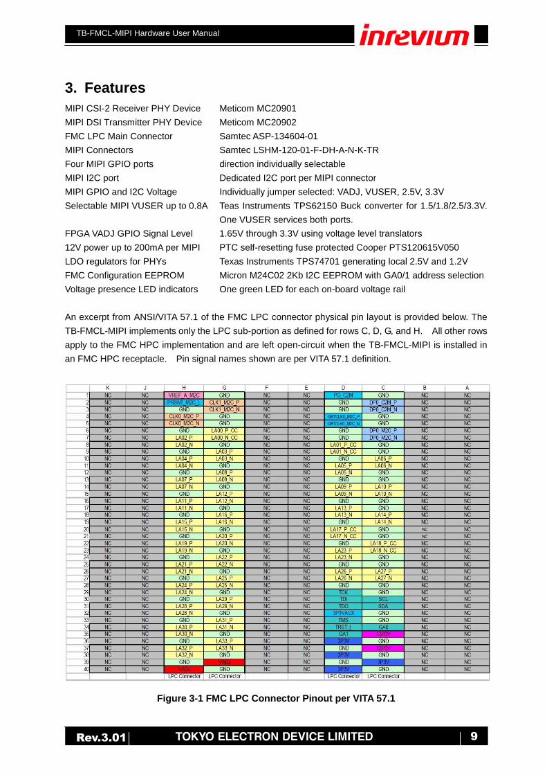
An excerpt from ANSI/VITA 57.1 of the FMC LPC connector physical pin layout is provided below. The
TB-FMCL-MIPI implements only the LPC sub-portion as defined for rows C, D, G, and H. All other rows
apply to the FMC HPC implementation and are left open-circuit when the TB-FMCL-MIPI is installed in
an FMC HPC receptacle. Pin signal names shown are per VITA 57.1 definition.
Figure 3-1 FMC LPC Connector Pinout per VITA 57.1

TB-FMCL-MIPI Hardware User Manual
10 Rev.3.01
4. Block Diagram
Figure 4-1 shows the TB-FMCL-MIPI block diagram.
FM
C L
ow
Pin
Count
Connecto
r A
SP
-134604-01
SN74AVC4T245 level translators use VADJ for the FMC connector side and 2.5V for the bridge side.
MC20901 5 Channel
MIPI CSI-2 Bridge
M24C02 EEPROM
3P3VAUXGA0GA1SDASCLTDITDO
GPIO-1
BTA
GPIO-0
PINSWAPSN74AVC4T245
SN74AVC4T245
SN74AVC4T245
HS-E_P/N
MC20902 5 Channel MIPI DSI Bridge
HS-D_P/NHS-C_P/NHS-B_P/NHS-A_P/N
LP-E_P
LP-D_P
LP-C_P
LP-B_NLP-A_P
GPIO-1
BTA
GPIO-0
PINSWAPSN74AVC4T245
SN74AVC4T245
SN74AVC4T245
LP-B_P
LP-C_N
LP-D_N
LP-E_N
LP-A_N
SN74AVC4T245
Section 1
Section 2
SN74AVC2T245
SN74AVC2T245
AUX_nOE1-4
12.0V VUSER 1.2V 2.5V
TPS74701 LDO TPS74701 LDO
VUSER jumper selectable for 1.5V, 1.8V, 2.5V, or 3.3V
12V0
VUSER
DSI MIPI PORT B
CSI-2 MIPI PORT A
SA
MT
EC
LS
HM
-12
0-0
1-F
-DH
-A-N
-K-T
RS
AM
TE
C L
SH
M-1
20
-01
-F-D
H-A
-N-K
-TR
TPS62150 SWITCHER
3.3V
I2C SDAI2C SCL
AUX_nOE5-8
MAX. 800mA Max. Draw 30mA Max. Draw 60mA
LP-D_P
LP-C_P
LP-B_NLP-B_P
LP-C_N
LP-D_N
HS-E_P/NHS-D_P/NHS-C_P/NHS-B_P/NHS-A_P/N
D-PHY-A_P/ND-PHY-B_P/ND-PHY-C_P/ND-PHY-D_P/ND-PHY-E_P/N
D-PHY-A_P/ND-PHY-B_P/ND-PHY-C_P/ND-PHY-D_P/ND-PHY-E_P/N
1.2V
2.5V
1.2V
2.5V
12.0V
3.3V
VADJ
2.5V & 1.2V
STATUS LEDs
I2C SDAI2C SCL
All CSI-2 and DSI MIPI Port SLVS, control, and I2C signals have ESD protection devices (not shown).
Four optional control bits set by jumpers to VADJ, 2.5V, 3.3V, or VUSER levels
VADJ = 1.8V or 2.5V
Transition boards or cables are used between the
Samtec LSHM connectors and the camera or display.
FXMA2102 I2C LEVEL TRANSLATOR
I2C Voltage set by jumpers to 1.8V, 2.5V, 3.3V, or
VUSER levels
FXMA2102 I2C LEVEL TRANSLATOR
I2C Voltage set by jumpers to VADJ, 2.5V, 3.3V, or
VUSER levels
Four optional control bits set by jumpers to VADJ, 2.5V, 3.3V, or VUSER levels
VUSER
3.3V_AUX
DIR
LP-E_PLP-E_N
SN74AVC4T245
Section 1
Section 2
DIR
10-pin header for DSI power, I2C and optional control bits
10-pin header for CSI power, I2C and optional control bits
LP-A_NLP-A_P
John Curnow 2014/08/06
SN74AVC2T245
IOEXPANDER
SN74AVC2T245
U10
U5
3V3
12V0
VUSER
3V3
Figure 4-1 TB-FMCL-MIPI Block Diagram

TB-FMCL-MIPI Hardware User Manual
11 Rev.3.01
5. External View of the Board
MIPI PORTB
GPIO DEBUG HDR J18
MIPI PORTB
MIPI AUX IO VOLTAGE
SELECTOR J19
MIPI PORTB
DSI CONNECTOR J16
MIPI PORTA
CSI CONNECTOR J5
MIPI PORTA
GPIO DEBUG
HDR J15
FMC LPC
CONNECTOR J1
MIPI PORTA/PORTB
PIN SWAP HDR J3
MIPI PORTA
MIPI AUX IO VOLTAGE
SELECTOR J12MIPI PORTB
I2C VOLTAGE
SELECTOR J17
VUSER VOLTAGE
SELECTOR J9
MIPI PORTA
I2C VOLTAGE
SELECTOR J6
Figure 5-1 Photo of TB-FMCL-MIPI (Side 1)

TB-FMCL-MIPI Hardware User Manual
12 Rev.3.01
Figure 5-2 Photo of TB-FMCL-MIPI (Side 2)

TB-FMCL-MIPI Hardware User Manual
13 Rev.3.01
6. Board Specification
The following shows the TB-FMCL-MIPI board physical specifications.
External Dimensions 76.50 mm L x 69.00 mm W – Dimensions/features per VITA57.1
Number of Layers 10 layers
Board Thickness 1.6 mm
Material Megtron 4
FMC LPC Connector Samtec ASP-134604-01
MIPI Connectors Samtec LSHM-120-01-F-DH-A-N-K-TR
Note: Refer to samtec.com for mating connector for
CL
63
.00
66.0
0
10.90
65.60
54.60
2.2
0
43.0
4
61.3
0
18.5
4
3.0
057.90
59
.05
58.3
0
Ø2.7, 6plcs
3.0
0
0.8
0
CL
Figure 6-1 TB-FMCL-MIPI Board Dimensions (mm)
Notes:
Board outline features conform to VITA57.1 air-cooled commercial grade single-width modules
MIPI connectors are pitched at 24.50mm center-to-center.
CSI position is defined as MIPI Port A, DSI position is defined as MIPI Port B
Board component side is defined in VITA 57.1 as Side 1 and faces the host carrier card when installed
Board solder side is defined as Side 2 and is probing and visually accessible when the card is installed

TB-FMCL-MIPI Hardware User Manual
14 Rev.3.01
7. Board Power System
7.1. Power System Overview
Figure 7-1 shows the TB-FMCL-MIPI power supply structure. The card uses the 12 Volt, the 3.3 Volt, the
3.3V AUX, and the VADJ rails supplied on the FMC connector from the carrier card. There is one 1.2V
LDO regulator to generate the PHY core voltage (MC20901/MC20902), one 2.5V LDO regulator for the
PHY IOs, and one switching regulator to generate the MIPI VUSER voltage rail. VADJ can range from
1.65V to 3.3V and is used mainly for the GPIO and I2C voltage translators. There is no control of power
sequencing. The 12V and 3.3V rails are protected by 0.5Amp PTC resettable fuses. If either fuse trips
due to an overcurrent fault, remove power to the card and wait a minute for the fuse to cool. Remove the
condition causing the excess current and apply power. If the fuse trips again, remove power, wait for the
fuse to cool, remove the card from the carrier, and contact our sales personnel for repair.
FMC LPC
CONNECTOR
12V0.5A PTC
3.3V0.5A PTC
3.3V AUX EEPROM
I2C I/O
EXPANDER
VADJ
Adjustable
Buck Switching
Regulator
GPIO
LEVEL
SHIFTERS
I2C
LEVEL
SHIFTERS
GPIO
LEVEL
SHIFTERS
VADJ
I2C
LEVEL
SHIFTERS
VUSER
3V32V5VADJ
3V32V5VADJVUSER
VUSER
LDO
Regulator2V5
LDO
Regulator1V2
1V51V82V53V3
VUSER
SELECTION
MIPI PORT 1
IO VOLTAGE
SELECTION
MIPI PORT A
MIPI PORT B
12V0
3V3_AUX
MIPI PORT 2
IO VOLTAGE
SELECTION
3V3
Figure 7-1 TB-FMCL-MIPI Power Structure
7.2. MIPI User Power Rail
The MIPI User power source connector power is supplied from a Texas Instruments TPS62150 switching
regulator. It provides four user selectable output voltages from 1.5V to 3.3V at a total current of 800mA,
or 400mA per MIPI port. The VUSER voltage does not necessarily need to reflect the MIPI IO logic
levels, however, it is available as one of the level shifter reference options. The VUSER selection
jumper is mapped as follows:
1
3.3V
2
3 4
5 6
7 8
1
2.5V
2
3 4
5 6
7 8
1
1.8V
2
3 4
5 6
7 8
1
1.5V
2
3 4
5 6
7 8
Figure 7-2 VUSER Jumper Select Positions
Note: Positioning more than one shunt, or positioning a shunt in a position not described above could
result in permanent damage to the board.

TB-FMCL-MIPI Hardware User Manual
15 Rev.3.01
7.3. LDO regulators
There are two Texas Instruments TPS74701 LDO regulators that are used to support the MIPI PHY
devices. The 1.2V regulator will need to supply up to 30mA to two PHY devices core supply in full
operation, and the 2.5V regulator will supply up to 60mA to two PHY devices IO supply in full operation.
In addition to the PHYs, the 2.5V regulator may also see an additional 72mA maximum loading from all
MIPI GPIO and 4.5mA maximum loading from MIPI I2C pullups if 2.5V is selected as the IO voltage
option for all the MIPI GPIO and I2C ports. Note that the TPS74701 requires a bias voltage of 1.3V
greater than the output voltage, thus the 2.5V regulator requires a bias input of at least 3.8V. Since
there is no 5V rail available, the bias input is generated by a zener diode from the FMC 12V power. The
zener regulation system draws 4.6mA (typ) to account for Bias current variation while still providing
sufficient reverse zener current to establish a stable voltage of approximately 4.3V.
The regulators each provide a Power-Good output; these open-collector outputs are tied together and
used as the control for the shared 2.5V and 1.2V LED indicator D4.
7.4. LED Power Indicators
A series of six green LEDs are located in a row on Side 2 (solder side) so they are visible when the card
is installed on an FMC carrier. The LEDs indicate the presence of the various supply rails, and under
normal conditions, all six LEDs should be lit when the card is powered-up. The following diagram of the
solder side displays the row of LEDs and their meaning:
12
V0
3V
3
3V
3_V
AU
X
2V
5 &
1V
2
VA
DJ
VU
SE
R
Figure 7-3 Power LEDs Identification
8. MIPI PHY Device to FMC Interface
8.1. PHY Device Overview
The PHY devices are produced by Meticom GmbH in both Receiver (MC20901) and Transmitter
(MC20902) versions. The devices draw very little power in operation and do not require any special
cooling considerations. The Meticom chip pinouts are designed to be mirrored between the Transmitter
(DSI) device, and Receiver (CSI-2) device. This permits a direct top-bottom PCB placement of the two
types while maintaining a fixed order and polarity of the MIPI differential pairs running to the connector.
This avoids signal integrity measures that would otherwise be needed in layout design to support the
dual CSI-2 or dual DSI assembly options.
8.2. HS Mode Interface
The FMC HS interface to the PHY devices consists of five differential pairs per MIPI port, totaling 10 IO
pins each. These signals are termed by Meticom as LVDS HS(0-4) and are the high-speed data
connection that carries MIPI payload data at up to Gb/s speeds. Typically, four lanes are assigned as

TB-FMCL-MIPI Hardware User Manual
16 Rev.3.01
data and one lane is assigned as clock. The HS mode data lanes operate in DDR mode with respect to
the clock, with one data bit transferred per clock transition. The Receiver (CSI-2) converts five low-swing,
high-speed differential signals (SLVS per Meticom’s terminology) to five LVDS links (4-data, 1-clock) sent
to the FMC LPC connector. The Transmitter (DSI) converts five LVDS links from the FMC LPC connector
to five SLVS links. Refer to the respective device datasheet for more details regarding electrical
characteristics and performance.
8.3. LP Mode Interface
Each PHY device also presents an alternate set of differential IOs, termed the CMOS LP(0-4). These
pins operate at LVCMOS level determined by VADJ, at up to 10Mb/s, and are active during Low-Power
(LP) mode transactions defined in the MIPI Specification. Low-power mode additionally features Bus
Turn Around (BTA) where the data direction on one of the CMOS LP links (Lane 0) is reversed to provide
host system read/write access to status and control registers from either a DSI (display) or CSI-2
(camera) MIPI peripheral. This facility supports minimized peripheral connectivity where additional
GPIOs, I2C or other side-band control links are absent.
8.4. PHY Control
Each PHY device presents a group of four control inputs to the host which govern the operation of the
MIPI link. Two pins, called GPIO-1 and GPIO-2, set the operating state of the PHY. Another input pin,
BTA, enables the Bus Turn Around (in LP) mode and is used for host access to status and control
registers within the peripheral device. The final input pin, called PINSWAP, is a three-mode input which
controls the differential polarity of all five MIPI lanes simultaneously. The following table outlines the
operating modes of the PHY device as selected by the input settings:
Table 8-1 MIPI PHY Mode Settings
Input Pins Mode
GPIO-1 GPIO-0 BTA PINSWAP
0 0 X X IC Power Down
0 1 X X SLVS-LVDS conversion unconditionally active
1 0 0 X MIPI D-PHY mode, BTA not Active during LP
1 0 1 X MIPI D-PHY mode, BTA Active on PHY channel E during LP
0 1 0 X *MIPI D-PHY mode, BTA not Active during LP
0 1 1 X *MIPI D-PHY mode, BTA Active on PHY channel A during LP
X X X 0 No HS Pin polarity Swaps
X X 0 1 HS Pin polarity swap each lane at the MIPI port
X X 1 1 No HS Pin polarity Swaps
X X X **Floating HS Pin polarity swap each lane at the LVDS HS port
* BTA on Channel A / MIPI lane 4 is not supported on the TB-FMCL-MIPI card. These settings should not
be used.
** This option is available by removing the appropriate shorting jumper from J3: pins 1-2 for CSI, pins 3-4
for DSI. Removed jumpers may be parked on unconnected pins 5-6 and 7-8. The user must ensure
that the jumpers are installed across pins 1-2 and 3-4 to select No Pin Swap mode.

TB-FMCL-MIPI Hardware User Manual
17 Rev.3.01
9. MIPI IO Signals
9.1. MIPI D-PHY Lanes
Each MIPI connector, whether input (CSI-2) or output (DSI), provides five differential pairs that are
designed to interface to 100-ohm differential wiring to the MIPI peripheral. The differential pairs are
assigned per Samtec’s recommendations for the LSHM series where each pair occupies adjacent pins
bounded on both sides by GND pins. For signal integrity reasons, in the 20-pin by 2-row connector pin
matrix, the high-speed differential lanes occupy the inside row, or “short” path (ROW 1), of the connector.
All five lanes from a connector to PHY device IO pads are delay matched to 10ps to minimize the PCB
impact on signal/clock timing relationship. Both the CSI and DSI port traces are approximately 31mm in
length, measured from the Meticom PHY pins to the LSHM connector.
9.2. MIPI GPIO Signals
Each MIPI connector is supplied with four GPIO signals that are supplied from SelectIO pins on the FMC
connector, as per the following diagram:
GA1
3.3V AUX
MIPI PORTA
MIPI PORTB
GA0 A0
A1
A2
3.3V AUX
ADDR: 01111xx
SDASCL
BI-DIR
LEVEL
SHIFTER
VADJ VADJ
VADJ
DIR
1
DIR
2
A1
A2
B1
B2
OEn
BI-DIR
LEVEL
SHIFTER
VADJ
DIR
1
DIR
2
A1
A2
B1
B2
OEn
DIR_MIPI_AUXIO_LPC3DIR_MIPI_AUXIO_LPC4
MIPI_AUXIO_LPC1
MIPI_AUXIO_LPC2
MIPI_AUXIO_nOE1-4
MIPI_AUXIO_LPC3
MIPI_AUXIO_LPC4
MIPI_AUXIO1
MIPI_AUXIO2
MIPI_AUXIO3
MIPI_AUXIO4
I2C I/O
EXPANDER
DIR_MIPI_AUXIO_LPC3
DIR_MIPI_AUXIO_LPC4
DIR_MIPI_AUXIO_LPC5
DIR_MIPI_AUXIO_LPC6
DIR_MIPI_AUXIO_LPC7
DIR_MIPI_AUXIO_LPC8
DIR_MIPI_AUXIO_LPC1
DIR_MIPI_AUXIO_LPC2
BI-DIR
LEVEL
SHIFTER
VADJ
A1
A2
B1
B2
OEn
BI-DIR
LEVEL
SHIFTER
VADJ
DIR
1
DIR
2
A1
A2
B1
B2
OEn
DIR_MIPI_AUXIO_LPC7DIR_MIPI_AUXIO_LPC8
MIPI_AUXIO_LPC5
MIPI_AUXIO_LPC6
MIPI_AUXIO_nOE5-8
MIPI_AUXIO_LPC7
MIPI_AUXIO_LPC8
MIPI_AUXIO5
MIPI_AUXIO6
MIPI_AUXIO7
MIPI_AUXIO8
DIR
1
DIR
2
DIR_MIPI_AUXIO_LPC5DIR_MIPI_AUXIO_LPC6
VUSER
3V32V5VADJ
VUSER
3V32V5VADJ
Figure 9-1 GPIO SIGNALS TO EACH MIPI PORT
The VADJ IO voltage domain of the FMC is level shifted to the user selected MIPI IO voltage domain
using Texas Instruments SN74AVC2T245 bi-directional dual-voltage transceivers. These devices can
operate to voltages as low as 1.2V, allowing the MIPI GPIO signals to support VADJ or VUSER down to
1.5V (actual minimum VADJ is 1.65V due to I2C translator limitations). Two FPGA pins on the FMC
connector control the output enable (OEn) of the level shifters (OEn=1 results in Hi-Z on each side of
translator). Each MIPI connector GPIO group can have its MIPI IO voltage selected from four options as

TB-FMCL-MIPI Hardware User Manual
18 Rev.3.01
shown:
1
3.3V
2
3 4
5 6
7 8
1
2.5V
2
3 4
5 6
7 8
1
VADJ
2
3 4
5 6
7 8
1
VUSER
2
3 4
5 6
7 8
Figure 9-2 MIPI GPIO Voltage Select Options
Each GPIO group has a header for voltage selection; MIPI PORT A (CSI-2) MIPI_AUXIO_(1-4) uses
header J12, and MIPI PORT B (DSI) MIPI_AUXIO_(5-8) uses header J19.
The direction of each of the eight GPIOs is determined by the Carrier Card FPGA via the MIPI FMC’s I2C
I/O Expander (Texas Instruments, PCA9534A). The I/O Expander is powered by 3V3_AUX and is
located on the dedicated FMC I2C bus at address: 01111xx (xx is determined by the FMC slot signals
GA[0:1]; GA0 → A1, GA1 → A0). The I/O Expander’s GPIOs default to input upon power up. Once
configured, when direction control pin is “high”, the GPIOs are outputs driven to the MIPI Port connector.
When the direction control pin is “low”, the GPIOs are inputs driven from the MIPI Port connector.
To help avoid contention, the recommended configuration sequence for the I/O Expander and Buffers
are as follows:
Table 9-1 GPIO Signals: Recommended sequencing
Stage Action Signals
T0 Power-Up, FPGA Configuration MIPI_AUXIO_nOE1-4 = 1
MIPI_AUXIO_nOE5-8 = 1
DIR_MIPI_AUXIO_LPC[1:8]= X (don’t Care)
MIPI_AUXIO_LPC[1:8] = X (don’t care)
Notes:
1. Both OE signals have resistor pull-ups to VADJ
2. Direction control signals have resistor pull-downs
T1 Program I/O Expander MIPI_AUXIO_nOE1-4 = 1
MIPI_AUXIO_nOE5-8 = 1
DIR_MIPI_AUXIO_LPC[1:8]= As required
T2 Start GPIO Signals MIPI_AUXIO_nOE1-4 = 1
MIPI_AUXIO_nOE5-8 = 1
DIR_MIPI_AUXIO_LPC[1:8]= As required
MIPI_AUXIO_LPC[1:8] = As required
T3 Enable Level Translators MIPI_AUXIO_nOE1-4 = 0
MIPI_AUXIO_nOE5-8 = 0
DIR_MIPI_AUXIO_LPC[1:8]= As required
MIPI_AUXIO_LPC[1:8] = As required

TB-FMCL-MIPI Hardware User Manual
19 Rev.3.01
9.3. MIPI I2C Bus
Each MIPI Port connector provides a standard I2C bus to any peripheral device that may be able to use
it (typically devices that do not utilize the MIPI BTA capability). Each connector receives its own set of
SelectIO pin assignments on the FMC connector, thus there is no I2C bus sharing on either MIPI port,
providing complete flexibility for MIPI device slave address assignment. The I2C bus of each port is IO
Voltage level selectable through headers J6 for the CSI port (MIPI Port A) and header J17 for the DSI
port (MIPI Port B). The jumper selection positions are identical to that of the GPIO selector headers
J12 and J19, detailed earlier in Figure 9-2. Note that the I2C translation buffer only supports voltages
down to 1.65V; the user must not to select a lower VUSER or VADJ voltage if the MIPI I2C is used.
However, if the I2C is not used, it is not harmful for VUSER or VADJ, if selected, to be below 1.65V as
long as the I2C port is not expected to operate.
10. Connectors
There are three main connectors on the TB-FMCL-MIPI card. One LPC FMC connector (J1) provides the
FMC host carrier interconnection, and the other two connectors (J5 and J16) are two right-angle MIPI
port sockets facing off the front edge (I/O window) of the FMC module. Additionally, for debug and
development access, two right angle headers, J15, and J18, located behind the MIPI port sockets and
facing out to the board side edges, provide access to the MIPI GPIO and I2C signals as well as VUSER
and 12V0.
10.1. LPC FMC Connector to Host Carrier Board
The LPC FMC connector (J1) used to mate to the Host Carrier Board is a Samtec ASP-134604-01. Only
the 160-pin LPC positions are populated, however, the module may be installed on a supported HPC
receptacle.
Table 10-1 shows the FMC connector pin assignment. In this table the C2M direction means
Carrier-to-Mezzanine, representing an input to the FMC. The M2C direction means Mezzanine-to-Carrier,
representing an output from the FMC. BIDIR identifies those signals whose direction can be application
selected. Signal Direction and Description in brackets represent MIPI port option assembly. Default
assembly shown is CSI-DSI (MIPI 1 – MIPI 2). Unused LAxx, DPx, and GBTCLKx signals are not
included in the table and are left unconnected. Power and GND pins are also not included; refer to
Figure 3-1 for power and ground pin connections.
FPGA IO allocations to FMC IO pins are platform specific and not included in the following table.
Please refer to the user manual of the particular FMC carrier host FPGA platform being used for the
mapping of FMC IOs to FPGA banks and pins.

TB-FMCL-MIPI Hardware User Manual
20 Rev.3.01
Table 10-1 LPC FMC Host Board Connector Pin Assignment
J1
Pin
Schematic Signal
Name
VITA 57.1 Pin
Name Direction Type Description
MIPI HS Signals
C18 M2C_LVDS_HS0_P LA14_P M2C LVDS
MIPI CSI PHY HS
Channel E C19 M2C_LVDS_HS0_N LA14_N
H13 M2C_LVDS_HS1_P LA07_P M2C LVDS
MIPI CSI PHY HS
Channel D H14 M2C_LVDS_HS1_N LA07_N
C14 M2C_LVDS_HS2_P LA10_P M2C LVDS
MIPI CSI PHY HS
Channel C C15 M2C_LVDS_HS2_N LA10_N
H16 M2C_LVDS_HS3_P LA11_P M2C LVDS
MIPI CSI PHY HS
Channel B H17 M2C_LVDS_HS3_N LA11_N
G6 **M2C_LVDS_HS4_P LA00_CC_P M2C LVDS
MIPI CSI PHY HS
Channel A G7 **M2C_LVDS_HS4_N LA00_CC_N
G24 C2M_LVDS_HS0_P LA22_P C2M LVDS
MIPI DSI PHY HS
Channel E G25 C2M_LVDS_HS0_N LA22_N
H22 C2M_LVDS_HS1_P LA19_P C2M LVDS
MIPI DSI PHY HS
Channel D H23 C2M_LVDS_HS1_N LA19_N
G21 C2M_LVDS_HS2_P LA20_P C2M LVDS
MIPI DSI PHY HS
Channel C G22 C2M_LVDS_HS2_N LA20_N
H25 C2M_LVDS_HS3_P LA21_P C2M LVDS
MIPI DSI PHY HS
Channel B H26 C2M_LVDS_HS3_N LA21_N
D20 **C2M_LVDS_HS4_P LA17_CC_P C2M LVDS
MIPI DSI PHY HS
Channel A D21 **C2M_LVDS_HS4_N LA17_CC_N
H4 CLK0_M2C_P CLK0_M2C_P
M2C LVDS
Optional MIPI CSI PHY
HS
Channel A H5 CLK0_M2C_N CLK0_M2C_N
G2 CLK1_M2C_P CLK1_M2C_P
C2M LVDS
Optional MIPI DSI PHY
HS
Channel A G3 CLK1_M2C_N CLK1_M2C_N
** inrevium strap option: route HS4 pairs to alternate clock FMC CLKx_M2C pins instead of LAxx_CC pins
MIPI LP Signals
G18 M2C_CMOS_BTA_LP0_P LA16_P M2C/C2M
LVCMOS
(VADJ)
MIPI CSI PHY LP
Channel E (BTA) G19 M2C_CMOS_BTA_LP0_N LA16_N
G15 M2C_CMOS_LP1_P LA12_P M2C LVCMOS
(VADJ)
MIPI CSI PHY LP
Channel D G16 M2C_CMOS_LP1_N LA12_N
G12 M2C_CMOS_LP2_P LA08_P M2C LVCMOS
(VADJ)
MIPI CSI PHY LP
Channel C G13 M2C_CMOS_LP2_N LA08_N
G9 M2C_CMOS_LP3_P LA03_P M2C
LVCMOS
(VADJ)
MIPI CSI PHY LP
Channel B G10 M2C_CMOS_LP3_N LA03_N
H7 M2C_CMOS_LP4_P LA02_P M2C
LVCMOS
(VADJ)
MIPI CSI PHY LP
Channel A H8 M2C_CMOS_LP4_N LA02_N
D23 C2M_CMOS_BTA_LP0_P LA23_P C2M/M2C
LVCMOS
(VADJ)
MIPI DSI PHY LP
Channel E (BTA) D24 C2M_CMOS_BTA_LP0_N LA23_N
TB-FMCL-MIPI Hardware User Manual
21 Rev.3.01
J1
Pin
Schematic Signal
Name
VITA 57.1 Pin
Name Direction Type Description
D26 C2M_CMOS_LP1_P LA26_P C2M LVCMOS
(VADJ)
MIPI DSI PHY LP
Channel D D27 C2M_CMOS_LP1_N LA26_N
H31 C2M_CMOS_LP2_P LA28_P C2M
LVCMOS
(VADJ)
MIPI DSI PHY LP
Channel C H32 C2M_CMOS_LP2_N LA28_N
G27 C2M_CMOS_LP3_P LA25_P C2M
LVCMOS
(VADJ)
MIPI DSI PHY LP
Channel B G28 C2M_CMOS_LP3_N LA25_N
G30 C2M_CMOS_LP4_P LA29_P C2M
LVCMOS
(VADJ)
MIPI DSI PHY LP
Channel A G31 C2M_CMOS_LP4_N LA29_N
PHY Control Signals
D11 CSI_GPIO0_LPC LA05_P C2M LVCMOS
(VADJ) MIPI 1 PHY GPIO Mode
control bits D12 CSI_GPIO1_LPC LA05_N C2M
LVCMOS
(VADJ)
C10 CSI_BTA_LPC LA06_P C2M LVCMOS
(VADJ) MIPI 1 PHY BTA Enable
C11 CSI_PNSWP_LPC LA06_N C2M LVCMOS
(VADJ)
MIPI 1 PHY Pin Swap
Enable
G33 DSI_GPIO0_LPC LA31_P C2M LVCMOS
(VADJ) MIPI 2 PHY GPIO Mode
control bits G34 DSI_GPIO1_LPC LA31_N C2M
LVCMOS
(VADJ)
C26 DSI_BTA_LPC LA27_P C2M LVCMOS
(VADJ) MIPI 2 PHY BTA Enable
C27 DSI_PNSWP_LPC LA27_N C2M LVCMOS
(VADJ)
MIPI 2 PHY Pin Swap
Enable
MIPI GPIO and I2C Signals
D14 MIPI_AUXIO_LPC1 LA09_P
per
MIPI_AUX_DI
R1
LVCMOS
(VADJ) MIPI Port A GPIO 1
D15 MIPI_AUXIO_LPC2 LA09_N
per
MIPI_AUX_DI
R2
LVCMOS
(VADJ) MIPI Port A GPIO 2
D17 MIPI_AUXIO_LPC3 LA13_P
per
MIPI_AUX_DI
R3
LVCMOS
(VADJ) MIPI Port A GPIO 3
D18 MIPI_AUXIO_LPC4 LA13_N
per
MIPI_AUX_DI
R4
LVCMOS
(VADJ) MIPI Port A GPIO 4
G36 MIPI_AUX_nOE1-4 LA33_P C2M LVCMOS
(VADJ)
MIPI Port A GPIO output
enable
H11 CLK_I2C_SCL_CSI_LPC_OD LA04_N C2M
LVCMOS
OD
(VADJ)
MIPI Port A I2C Clock
H10 I2C_SDA_CSI_LPC_OD LA04_P BIDIR LVCMOS MIPI Port A I2C Data

TB-FMCL-MIPI Hardware User Manual
22 Rev.3.01
J1
Pin
Schematic Signal
Name
VITA 57.1 Pin
Name Direction Type Description
OD
(VADJ)
H34 MIPI_AUXIO_LPC5 LA30_P
per
MIPI_AUX_DI
R5
LVCMOS
(VADJ) MIPI Port B GPIO 1
H35 MIPI_AUXIO_LPC6 LA30_N
per
MIPI_AUX_DI
R6
LVCMOS
(VADJ) MIPI Port B GPIO 2
H37 MIPI_AUXIO_LPC7 LA32_P
per
MIPI_AUX_DI
R7
LVCMOS
(VADJ) MIPI Port B GPIO 3
H38 MIPI_AUXIO_LPC8 LA32_N
per
MIPI_AUX_DI
R8
LVCMOS
(VADJ) MIPI Port B GPIO 4
G37 MIPI_AUX_nOE5-8 LA33_N C2M LVCMOS
(VADJ)
MIPI Port B GPIO
output enable
H20 CLK_I2C_SCL_DSI_LPC_OD LA15_N C2M
LVCMOS
OD
(VADJ)
MIPI Port B I2C Clock
H19 I2C_SDA_DSI_LPC_OD LA15_P BIDIR
LVCMOS
OD
(VADJ)
MIPI Port B I2C Data
FMC Facility Signals
C30 CLK_FMC_SCL_OD SCL C2M LVTTL
OD FMC IPMI EEPROM Clk
C31 FMC_SDA_OD SDA BIDIR LVTTL
OD
FMC IPMI EEPROM
Data
C34 GA0 GA0 C2M LVTTL
FMC IPMI EEPROM
slave address select
MSB
D35 GA1 GA1 C2M LVTTL
FMC IPMI EEPROM
slave address select
LSB
D1 FMC_PG_C2M PG_C2M C2M LVTTL Local LDO enable
H2 GND PRSNT_M2C_N M2C LVTTL
Card presence
(asserted)
D30
Loop back connection
TDI C2M LVTTL Looped JTAG data to
maintain carrier JTAG
loop D31 TDO M2C LVTTL
D29 Open TCK C2M LVTTL Not used
D33 Open TMS C2M LVTTL Not used
D34 Open TRST_N C2M LVTTL Not used
H1 TP1 testpoint VREF_A_M2C Testpoint access

TB-FMCL-MIPI Hardware User Manual
23 Rev.3.01
Note: If this FMC is to be connected to the inrevium TB-7V-2000T-LSI then populate R180 and R181
and depopulate R178 and R179, populate R184 and R185 and depopulate R182 and R183.
Figure 10-1 Resistor for connection to TB-7V-2000T-LSI

TB-FMCL-MIPI Hardware User Manual
24 Rev.3.01
10.2. MIPI Front Edge (I/O Window) Receptacles
The TB-FMCL-MIPI card utilizes Samtec Razor Beam™
LSHM series connectors for access to the MIPI
ports. These 0.5mm pitch receptacles provide 40 connections in mixed differential and single-ended
signals, in a format that is compact enough to fit two receptacles across a single-width FMC form-factor.
Each channel connector, in addition to the 4+1 MIPI lanes, provides 12V, 3.3V, and User Power
(on-board selectable voltage), an I2C link, and four General Purpose IOs. Using suitable adapter
modules, a MIPI camera sensor and/or low-power MIPI mobile display panel can be directly supported
without need for additional external connections. The two receptacles are located side-by-side at the
faceplate edge, with pinout as shown in the front view below in typical components-down orientation:
39
40
1
2PORT A
DFT=CSI DFT=DSI
PORT B39
40
1
2
Figure 10-2 MIPI Connectors Faceplate View
Note: These connectors offer good retention force, and provide an audible notification when properly
mated. During adapter insertion or extraction, “zippering” may cause irreparable damage to the
connectors and/or the solder joints. It is critical that the user insert and extract mating devices axially,
and avoid “zippering”.
Figure 10-3 Axial removal vs zippering (picture courtesy of Samtec®)

TB-FMCL-MIPI Hardware User Manual
25 Rev.3.01
The pinouts are provided in the following table:
Table 10-2 MIPI D-PHY PORT A J5 (CSI)
Connector J5 CSI (PORT A)
Pin Signal Pin Signal
1 GND 2 GND
3 NC (TEST POINT TP3) 4 MIPI_SLVS_IN4_N
5 NC (TEST POINT TP2) 6 MIPI_SLVS_IN4_P
7 GND 8 GND
9 LOOP_N 10 MIPI_SLVS_IN3_N
11 LOOP_P 12 MIPI_SLVS_IN3_P
13 GND 14 GND
15 MIPI_AUXIO_4 16 MIPI_SLVS_IN2_N
17 MIPI_AUXIO_3 18 MIPI_SLVS_IN2_P
19 GND 20 GND
21 MIPI_AUXIO_2 22 MIPI_SLVS_IN1_N
23 MIPI_AUXIO_1 24 MIPI_SLVS_IN1_P
25 GND 26 GND
27 I2C_SDA_MIPI_CSI_OD 28 MIPI_SLVS_IN0_BTA_N
29 CLK_I2C_SCL_MIPI_CSI_OD 30 MIPI_SLVS_IN0_BTA_P
31 GND 32 GND
33 VUSER 34 VUSER
35 GND 36 GND
37 3V3 38 3V3
39 GND 40 12V0
TB-FMCL-MIPI Hardware User Manual
26 Rev.3.01
Table 10-3 MIPI D-PHY PORT B J16 (DSI)
Connector J5 CSI (PORT A)
Pin Signal Pin Signal
1 GND 2 GND
3 NC (TEST POINT TP5) 4 MIPI_SLVS_OUT4_N
5 NC (TEST POINT TP4) 6 MIPI_SLVS_OUT4_P
7 GND 8 GND
9 LOOP_N 10 MIPI_SLVS_OUT3_N
11 LOOP_P 12 MIPI_SLVS_OUT3_P
13 GND 14 GND
15 MIPI_AUXIO_8 16 MIPI_SLVS_OUT2_N
17 MIPI_AUXIO_7 18 MIPI_SLVS_OUT2_P
19 GND 20 GND
21 MIPI_AUXIO_6 22 MIPI_SLVS_OUT1_N
23 MIPI_AUXIO_5 24 MIPI_SLVS_OUT1_P
25 GND 26 GND
27 I2C_SDA_MIPI_DSI_OD 28 MIPI_SLVS_OUT0_BTA_N
29 CLK_I2C_SCL_MIPI_DSI_OD 30 MIPI_SLVS_OUT0_BTA_P
31 GND 32 GND
33 VUSER 34 VUSER
35 GND 36 GND
37 3V3 38 3V3
39 GND 40 12V0
Note: LOOP_P and LOOP_N provide a passive method for two adapters to connect. Reserved for future
use.
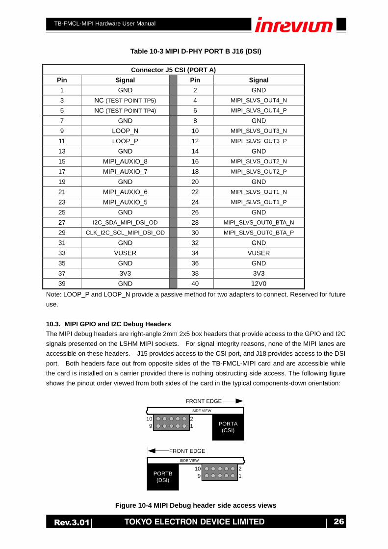
10.3. MIPI GPIO and I2C Debug Headers
The MIPI debug headers are right-angle 2mm 2x5 box headers that provide access to the GPIO and I2C
signals presented on the LSHM MIPI sockets. For signal integrity reasons, none of the MIPI lanes are
accessible on these headers. J15 provides access to the CSI port, and J18 provides access to the DSI
port. Both headers face out from opposite sides of the TB-FMCL-MIPI card and are accessible while
the card is installed on a carrier provided there is nothing obstructing side access. The following figure
shows the pinout order viewed from both sides of the card in the typical components-down orientation:
PORTA
(CSI)1
2
9
10
SIDE VIEW
FRONT EDGE
PORTB
(DSI)
SIDE VIEW
FRONT EDGE
1
2
9
10
Figure 10-4 MIPI Debug header side access views

TB-FMCL-MIPI Hardware User Manual
27 Rev.3.01
Table 10-4 MIPI GPIO Debug Headers J15 and J18
Header
J15 Pin Signal
Header
J18 Pin Signal
1 MIPI_AUXIO_1 1 MIPI_AUXIO_5
2 12V0 2 12V0
3 MIPI_AUXIO_2 3 MIPI_AUXIO_6
4 VUSER 4 VUSER
5 MIPI_AUXIO_3 5 MIPI_AUXIO_7
6 CLK_I2C_SCL_MIPI_CSI_O
D
6
CLK_I2C_SCL_MIPI_DSI_O
D
7 MIPI_AUXIO_4 7 MIPI_AUXIO_8
8 I2C_SDA_MIPI_CSI_OD 8 I2C_SDA_MIPI_DSI_OD
9 Ground 9 Ground
10 Ground 10 Ground
11. FMC Facility I2C Bus
11.1. FMC I2C EEPROM
A 2kbit I2C EEPROM (M24C02) is provided for FMC identification, as described in section 5.5 of
ANSI/VITA 57.1. It is at I2C address 0b1010000x and is connected to the FMC dedicated I2C pins at
J1-C30 (SCL) and J1-C31 (SDA). The pull-up resistors to 3V3_AUX are not populated (R148 and R149)
since the pull-ups should be provided on the carrier. The EEPROM is permanently enabled for writing.
The FMC identification EEPROM is programmed at the factory to enable automated identification,
verification, and configuration of Main Board parameters (typically VADJ voltage level). The contents of
the EEPROM are described in Appendix A.
Note: The user must be cognizant that the FMC I2C EEPROM is always write-enabled. As it contains
critical information required for correct operation, one must never overwrite the factory settings.
12. ESD Protection
All MIPI SLVS differential signals as well as the GPIO and I2C ports are protected with Texas
Instruments TPD1E05U06DPYT unidirectional ESD protection devices located close to the MIPI
receptacles. They provide IEC 61000-4-2 level 4 protection and are very low capacitance (0.5pF typical)
designed for up to 6Gbps speed interfaces. Applied to 100-ohm differential lines, these devices introduce
less than 1dB insertion loss up to 2GHz (4Gbps).
13. Demonstration
A reference load is available. Please ask your sales contact for additional information.

TB-FMCL-MIPI Hardware User Manual
28 Rev.3.01
14. Appendix A: FMC I2C EEPROM
The following table describes the contents of the FMC I2C EEPROM as programmed at the factory.
Table 14-1 FMC I2C EEPROM Contents
Board Information
Field Size Data
Language Code 1 0
Date / Time of Manufacture 3 <Variable>
Board Manufacturer 16 FidusSystemsInc
Board Product Name 16 TB-FMCL-MIPI
Board Serial Number 16 <Variable>
Board Part Number 16 PA-10087-xx
xx=01 for CSI/DSI
xx=02 for CSI/CSI
xx=03 for DSI/DSI
FRU File ID 1 0
Hardware Revision 6 <Variable>
MAC Address 6 00:00:00:00:00:00
Multi-Record Information
VITA Subtype 0 Record
Field Size Data Description
Vendor OUI 3 0x0012A2 Fixed value of 0x0012A2
Subtype/Version 1 0x00 7:4 (type): main definition type
3:0 (version): current version
Size/Connectors/Clock Dir 1 0x0C 7:6 (size): single width
5:4 (P1 size): LPC
3:2 (P2 size): not fitted
0 (clock dir): Mezzanine to Carrier
0: reserved 0
P1 Bank A Number Signals 1 0x42 66 signals
P1 Bank B Number Signals 1 0x00
P2 Bank A Number Signals 1 0x00
P2 Bank B Number Signals 1 0x00
P1/P2 Number Transceivers 1 0x00
Max Clock for TCK 1 0x95 In units of MHz: 149MHz

TB-FMCL-MIPI Hardware User Manual
29 Rev.3.01
DC Load Record – VADJ
Field Size Data Description
Output Information 1 0x00 Bit map containing output number, etc. (VADJ)
Nominal Voltage 2 0x00B4 In units of 10mV (1.8V)
Minimum Voltage 2 0x00A5 In units of 10mV (1.65V)
Maximum Voltage 2 0x014A In units of 10mV (3.3V)
Ripple and Noise (PK-PK) 2 0x0032 In units of 1mV (10Hz to 30MHz) (50mV)
Minimum Current Draw 2 0x0022 In units of 1mA (34mA)
Maximum Current Draw 2 0x0064 In units of 1mA (100mA)
DC Load Record – 3P3V
Field Size Data Description
Output Information 1 0x01 Bit map containing output number, etc. (3.3V)
Nominal Voltage 2 0x014A In units of 10mV (3.3V)
Minimum Voltage 2 0x0139 In units of 10mV (3.13V)
Maximum Voltage 2 0x0154 In units of 10mV (3.4V)
Ripple and Noise (PK-PK) 2 0x0032 In units of 1mV (10Hz to 30MHz) (50mV)
Minimum Current Draw 2 0x001E In units of 1mA (30mA)
Maximum Current Draw 2 0x0096 In units of 1mA (150mA)
DC Load Record – 12P0V
Field Size Data Description
Output Information 1 0x02 Bit map containing output number, etc. (12V)
Nominal Voltage 2 0x04B0 In units of 10mV (12V)
Minimum Voltage 2 0x0474 In units of 10mV (11.4V)
Maximum Voltage 2 0x04EC In units of 10mV (12.6V)
Ripple and Noise (PK-PK) 2 0x0064 In units of 1mV (10Hz to 30MHz) (100mV)
Minimum Current Draw 2 0x0023 In units of 1mA (35mA)
Maximum Current Draw 2 0x01F4 In units of 1mA (500mA)
DC Output Record – VIO_B_M2C (DOES NOT EXIST, LPC)
Field Size Data Description
Output Information 1 0x03 Bit map containing output number, etc.
Nominal Voltage 2 0x0000 In units of 10mV
Minimum Voltage 2 0x0000 In units of 10mV
Maximum Voltage 2 0x0000 In units of 10mV
Ripple and Noise (PK-PK) 2 0x0000 In units of 1mV (10Hz to 30MHz)
Minimum Current Load 2 0x0000 In units of 1mA
Maximum Current Load 2 0x0000 In units of 1mA

TB-FMCL-MIPI Hardware User Manual
30 Rev.3.01
DC Output Record – VREF_A_M2C (NOT CONNECTED)
Field Size Data Description
Output Information 1 0x04 Bit map containing output number, etc.
Nominal Voltage 2 0x0000 In units of 10mV
Minimum Voltage 2 0x0000 In units of 10mV
Maximum Voltage 2 0x0000 In units of 10mV
Ripple and Noise (PK-PK) 2 0x0000 In units of 1mV (10Hz to 30MHz)
Minimum Current Load 2 0x0000 In units of 1mA
Maximum Current Load 2 0x0000 In units of 1mA
DC Output Record – VREF_B_M2C (DOES NOT EXIST, LPC)
Field Size Data Description
Output Information 1 0x05 Bit map containing output number, etc.
Nominal Voltage 2 0x0000 In units of 10mV
Minimum Voltage 2 0x0000 In units of 10mV
Maximum Voltage 2 0x0000 In units of 10mV
Ripple and Noise (PK-PK) 2 0x0000 In units of 1mV (10Hz to 30MHz)
Minimum Current Load 2 0x0000 In units of 1mA
Maximum Current Load 2 0x0000 In units of 1mA

TB-FMCL-MIPI Hardware User Manual
31 Rev.3.01
15. Appendix B: Headers, Factory Default, and Orientation
The following depicts the factory default header jumper positions and clarifies the pin numbering and
orientation of the headers. Default strap selected functions are as follows:
Table 15-1 Default Header Explanation
Option Header Function Selected
J3 1-2: DSI_MIPI_PINSWP controlled by FPGA
3-4: CSI_MIPI_PINSWP controlled by FPGA
J6 7-8: MIPI PORT A CSI I2C set to VUSER IO voltage
J9 5-6: VUSER set to 1.8V
J12 7-8: MIPI PORT A MIPI_AUXIO_(1-4) set to VUSER IO voltage
J17 7-8: MIPI PORT B DSI I2C set to VUSER IO voltage
J19 7-8: MIPI PORT B MIPI_AUXIO_(5-8) set to VUSER IO voltage
J3
2
34
56
78
1
J12
2
34
56
78
1
J17
2
34
56
78
1
J9
2
34
56
78
1
J6
2
34
56
78
1
J19
2
345678
1
Figure 15-1 Default Jumper Positions and Header Orientation

TB-FMCL-MIPI Hardware User Manual
32 Rev.3.01
Inrevium Company URL: http://www.inrevium.com/ http://solutions.inrevium.com/
E-mail: [email protected] HEAD Quarter: Yokohama East Square, 1-4 Kinko-cho, Kanagawa-ku, Yokohama City,
Kanagawa, Japan 221-0056 TEL: +81-45-443-4031 FAX: +81-45-443-4063