table of contents 1. introduction 2. specification...
TRANSCRIPT

6BXA
1
TABLE OF CONTENTS
1. INTRODUCTION
1.1. PREFACE..........................................................................................................1-1
1.2. KEY FEATURES...............................................................................................1-1
1.3. PERFORMANCE LIST .....................................................................................1-2
1.4. BLOCK DIAGRAM ............................................................................................1-3
1.5. INTRODUCE THE Pentium II Processor & AGP..........................................1-4
1.6. What is AGP? ....................................................................................................1-5
2. SPECIFICATION
2.1. HARDWARE .....................................................................................................2-1
2.2. SOFTWARE......................................................................................................2-2
2.3. ENVIRONMENT................................................................................................2-2
3. HARDWARE INSTALLATION
3.1. UNPACKING.....................................................................................................3-1
3.2. MAINBOARD LAYOUT.....................................................................................3-2
3.3. QUICK REFERENCE FOR JUMPERS & CONNECTORS.............................3-2
3.4. DRAM INSTALLATION.....................................................................................3-6
3.5. CPU SPEED SETUP ........................................................................................3-7
3.6. CMOS RTC & ISA CFG CMOS SRAM ............................................................3-8
3.7. SPEAKER CONNECTOR INSTALLATION .....................................................3-8
3.8. HARDWARE RESET SWITCH CONNECTOR INSTALLATION ....................3-9
3.9. POWER LED CONNECTOR INSTALLATION ................................................3-9
3.10. IDE & ATAPI DEVICE INSTALLATION .........................................................3-9
Table of Contents
2
3.11. PERIPHERAL DEVICE INSTALLATION .......................................................3-9
3.12. KEYBOARD & PS/2 MOUSE INSTALLATION..............................................3-9
4. BIOS CONFIGURATION
4.1. ENTERING SETUP ..........................................................................................4-1
4.2. CONTROL KEYS..............................................................................................4-1
4.3. GETTING HELP................................................................................................4-2
4.3.1. Main Menu ............................................................................................4-2
4.3.2. Status Page Setup Menu / Option Page Setup Menu.........................4-2
4.4. THE MAIN MENU .............................................................................................4-2
4.5. STANDARD CMOS SETUP MENU .................................................................4-4
4.6. BIOS FEATURES SETUP................................................................................4-8
4.7. CHIPSET FEATURES SETUP.........................................................................4-13
4.8. POWER MANAGEMENT SETUP....................................................................4-17
4.9. PNP/PCI CONFIGURATION ............................................................................4-21
4.10. LOAD BIOS DEFAULTS.................................................................................4-23
4.11. LOAD PERFORMANCE DEFAULTS.............................................................4-24
4.12. INTEGRATED PERIPHERALS ......................................................................4-25
4.13. SUPERVISOR/USER PASSWORD...............................................................4-30
4.14. IDE HDD AUTO DETECTION........................................................................4-31
4.15. SAVE & EXIT SETUP.....................................................................................4-32
4.16. EXIT WITHOUT SAVING ...............................................................................4-33
6BXA
1-1
1. INTRODUCTION
1.1. PREFACE
Welcome to use the 6BXA motherboard. It is a Pentium II / CeleronProcessor based PC / AT compatible system with AGP/ PCI / ISA Bus, andhas been designed to be the fastest PC / AT system. There are some newfeatures allow you to operate the system with just the performance you want.
This manual also explains how to install the motherboard for operation, andhow to set up your CMOS CONFIGURATION with BIOS SETUP program.
1.2. KEY FEATURES
q Intel Pentium II / Celeron Processor based PC / AT compatiblemainboard.
q Slot 1 supports Pentium II / Celeron processor running at 233-633 MHz.
q Intel 440BX chipset, Supports SDRAM / Ultra DMA 33 IDE.
q Built-in PCI ESS SOLO 1 audio chip.
q Supports external Modem Ring-On on COM A&B and Internal.
q Supports Wake-up on LAN (JP10).
q Supports 3xDIMMs using 3.3V EDO or SDRAM DIMM module.
q Supports 16 MB - 768 MB SDRAM .
q 5xPCI Bus slots, 1xISA Bus slots, 1xAGP slot.
q Supports 2 channels Ultra DMA 33 IDE ports for 4 IDE Devices.
q Supports 2xCOM (16550), 1xLPT (EPP / ECP), 1x Floppy port.
q Supports 2xUSB ports, 1xPS/2 Mouse, 1xPS/2 Keyboard.
q Licensed AWARD BIOS, 2Mbits FLASH RAM.
q 30.5 cm x 19 cm ATX form factor, 4 layers PCB.

Introduction
1-2
1.3. PERFORMANCE LIST
The following performance data list is the testing results of some popularbenchmark testing programs.
These data are just referred by users, and there is no responsibility fordifferent testing data values gotten by users. (The different Hardware &Software configuration will result in different benchmark testing results.)
• CPU Pentium II processor
• DRAM (128 x 1) MB SDRAM (TOSHIBA TC59S6408FTL-80H)
• CACHE SIZE 512 KB included in CPU
• DISPLAY GA-630 voodoo banshee (16MB SGRAM)
• STORAGE Onboard IDE (IBM DHEA 36481)
• O.S. Windows NT ™ 4.0 SPK4
• DRIVER Display Driver at 1024 x 768 x 64K colors x 75Hz.
TRIONES Bus Master IDE Driver 3.70a
Intel Pentium IIProcessor
500MHz(100x5) 400MHz(100x4)
Winbench99
CPU mark32 1270 1080
FPU Winmark 2560 2070
Business Disk 4200 4070
Hi-End Disk 8210 8300
Business Graphics 228 198
Hi-End Graphics 408 345
Winstone99
Business 34.2 31.3
Hi-End 30.2 26.7

6BXA
1-3
3.3V EDO/SDRAMDIMM Sockets
Floppy Port
1.4. BLOCK DIAGRAM
Ultra DMA/33IDE Ports
Game Port PS/2 Keyboard
24MHz
33MHz
33MHz
33MHz
66MHz
66MHz
IDE Bus
PCI Bus
AGPBus
LPT Port
COM Ports
DRAM Bus
PS/2 Mouse
USB Bus
USB Ports14.318MHz
48MHz
14.318MHz
I/OCHIPSETIT8671F
Host Bus
PIIX 4CHIPSET
82443BXCHIPSET
ClockGenerator
MIC
L-IN
L-OUT
ESS
SOLO-1
14.318MHz
66MHz
AGPSlot
SLOT 1

Introduction
1-4
1.5. INTRODUCE THE Pentium II Processor & AGP
Figure 1:Retention Mechanism & attach Mount
Figure 2:OEM Pentium II Processor
6BXA
1-5
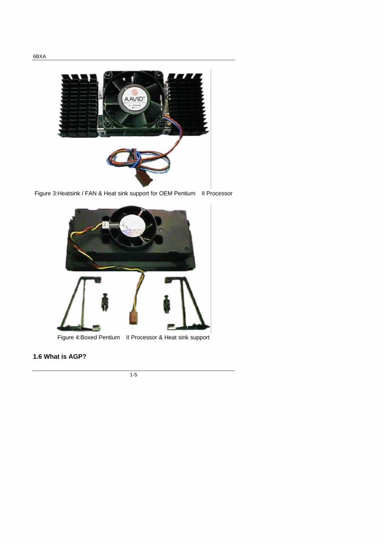
Figure 3:Heatsink / FAN & Heat sink support for OEM Pentium II Processor
Figure 4:Boxed Pentium II Processor & Heat sink support
1.6 What is AGP?

Introduction
1-6
The Accelerated Graphics Port (AGP) is a new port on the Host-To-PCIbridge device that supports an AGP port. The main purpose of the AGP port isto provide fast access to system memory.
The AGP port can be used either as fast PCI port (32-bits at 66MHz vs. 32-bits at 33MHz) or as an AGP port which supports 2x data-rate, a read queue,and side band addressing. When the 2x-data rate is used, the port cantransmit data at 533MB/sec (66.6*2*4). The read-queue can be used topipeline reads – removing the effects of the reads-latency. Side bandaddressing can be used to transmit the data address on a separate line inorder to speed up the transaction.

6BXA
2-1
2. SPECIFICATION
2.1. HARDWARE
• CPU− Pentium II / Celeron processor 233 – 633 MHz.− 242 pins 66 MHz slot1 on board.
• SPEED − 66/100 MHz system speed.− 66 MHz AGP bus speed. (2X mode 133MHz)− 33 MHz PCI-Bus speed.− 8 MHz AT bus speed.
• PROTECTION− Speaker Alarm when detect "CPU FAN Failure" or
“CPU Overheat”.− Automatically slow down CPU speed when "CPU
Overheat".− H/W monitor power status (±5V, ±12V, VCOREA,
VGTL, VCC3, VBAT, 5VSB voltage & CMOS batteryvoltage).(Optional)
• DRAM MEMORY − 3 banks 168 pins DIMM module sockets on board.− Use 16 / 32 / 64 / 128 / 256 MB DIMM module
DRAM.− 16 ~ 768MB SDRAM.− Supports 3.3V SDRAM / EDO type DRAM.
• CACHE MEMORY − 32 KB 1st cache memory included in CPU.− 256KB/512 KB 2nd cache in CPU.− Supports DIB speed mode for L2 Cache.
• I/O BUS SLOTS − 5 33MHz Master / Slave PCI-BUS.− 1 33MHz AGP BUS.− 1 8MHz 16 bits ISA BUS.
• IDE PORTS − 2 Ultra DMA 33 Bus Master IDE channels onboard.(Using IRQ14,15)
− Support Mode 3,4 IDE & ATAPI CD – ROM.
• Audio Ports − 1x Line in
− 1x Line out
− 1x Micro in
− 1x Game Port
− 2x CD Line in
− 1x TEL Port
Specification
2-2
• I/O PORTS − Supports 2 16550 COM ports.− Supports 1 LPT port.− Supports 1 Floppy port.− Supports 2 USB ports.− Supports 1 PS/2 Mouse.− Supports 1 PS/2 Keyboard.
• GREEN FUNCTION − Suspend mode support.− Green switch & Green LED support.− IDE & Display power down support.− Monitor all IRQ / DMA / Display / I/O events.
• BIOS − 2M bits FLASH RAM.− Supports Plug & Play, DMI Function.
• DIMENSION − ATX Form Factor, 4 layers PCB.
2.2. SOFTWARE
• DRIVER − Bus Master IDE Driver.
− INTEL Patch_95 Driver.
− ESS SOLO-1 Sound Driver.
• BIOS − Licensed AWARD BIOS.− AT CMOS Setup, BIOS / Chipset Setup, Green
Setup, Hard Disk Utility included.• O.S. − Operation with MS-DOS, Windows95,
Windows98, WINDOWS NT, OS/2, NOVELLand SCO UNIX.
2.3. ENVIRONMENT
• Ambient Temp. − 0°C to +50°C (Operating).• Relative Hum. − 0 to +85% (Operating).• Altitude − 0 to 10,000 feet (Operating).• Vibration − 0 to 1,000 Hz.• Electricity − 4.9 V to 5.2 V. (Max. 20A current at 5V.)
6BXA
3-1
3. HARDWARE INSTALLATION
3.1. UNPACKING
The mainboard package should contain the following:
• The 6BXA mainboard.
• The Retention Mechanism & Attach Mount
• USER'S MANUAL for mainboard.
• Cable set for IDE, Floppy devices.
• CD or diskette for Mainboard ¡ BSound and VGA Utility.
The mainboard contains sensitive electric components, which can be easilydamaged by static electricity, so the mainboard should be left in its originalpacking until it is installed.
Unpacking and installation should be done on a grounded anti-static mat. Theoperator should be wearing an anti static wristband, grounded at the samepoint as the anti-static mat.
Inspect the mainboard carton for obvious damage. Shipping and handlingmay cause damage to your board. Be sure there are no shipping and handlingdamages on the board before proceeding.
After opening the mainboard carton, extract the system board and place itonly on a grounded anti-static surface component side up. Again inspect theboard for damage. Press down on all of the socket IC's to make sure that theyare properly seated. Do this only on with the board placed on a firm flatsurface.
MDO NOT APPLY POWER TO THE BOARD IF IT HAS BEEN DAMAGED.

Hardware Installation
3-2
3.2. MAINBOARD LAYOUT6B
XA
ESSSOLO-1
INTEL443BX
PIIX4
BIOS
SLOT1
JP11
JP7CN 6
JP4
USB PS/2
JP18
JP9BAT1
J12
JP12 IR J9JP5
SW2 SW1
IDE 2
IDE 1
ATX POWER
FLOPPY
BANK 0
BANK 1BANK 2
GAME&AUDIO
COM A COM BLPT
BZ1
JP17
JP20
×Figure 3.1Ø
3.3. QUICK REFERENCE FOR JUMPERS & CONNECTORS
t I/O Ports ConnectorUSB USB port.IDE1 For Primary IDE port.IDE2 For Secondary IDE port.FLOPPY For Floppy portPS/2 For PS/2 Keyboard / Mouse port.COMB For Serial port2 (COM B).COMA For Serial port1 (COM A).LPT For LPT port.GAME For GAME port.ATX Power For ATX Power Connector.AUDIO For MIC,LINE-IN,LINE-OUT port.
t Slot 1For Pentium II / Celeron processor installed
6BXA
3-3
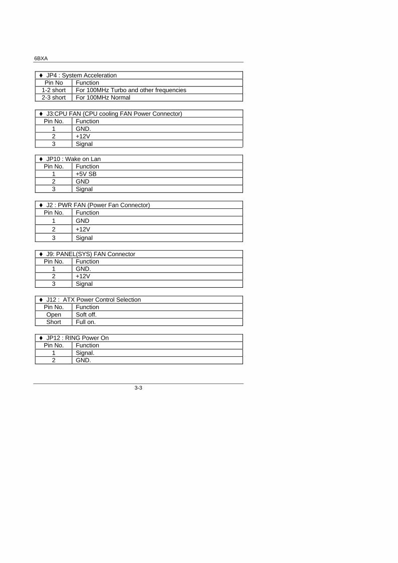
t JP4 : System AccelerationPin No Function
1-2 short For 100MHz Turbo and other frequencies2-3 short For 100MHz Normal
t J3:CPU FAN (CPU cooling FAN Power Connector)Pin No. Function
1 GND.2 +12V3 Signal
t JP10 : Wake on LanPin No. Function
1 +5V SB2 GND3 Signal
t J2 : PWR FAN (Power Fan Connector)Pin No. Function
1 GND2 +12V3 Signal
t J9: PANEL(SYS) FAN ConnectorPin No. Function
1 GND.2 +12V3 Signal
t J12 : ATX Power Control SelectionPin No. FunctionOpen Soft off.Short Full on.
t JP12 : RING Power OnPin No. Function
1 Signal.2 GND.

Hardware Installation
3-4
t JP13 : Clear CMOSPin No. Function
1-2 Short Clear CMOS.2-3 Short NORMAL.
t JP18 / JP19 : Onboard Sound Function SelectionPin No. Function
1-2 Close Onboard Sound Function Enabled.2-3 Close Onboard Sound function Disabled.
t JP17 : Onboard Sound Function SelectionPin No. Function
1.2 & 3.4 Open Onboard Sound Function Enabled.1.2 & 3.4 Close Onboard Sound function Disabled.
t JP1 : Keyboard Power On SelectionPin No. Function
1-2 Close Enabled Keyboard power on.2-3 Close Disabled Keyboard power on.
t JP11 : CASE OPEN (Optional)Pin No. Function
1 Signal2 GND
t IR: INFRARED Connector (OPTIONAL)Pin No. Function
1 IR Data Output2 GND3 IR Data Input4 NC5 POWER (+)
t JP14: Suspend To RAM Function (Optional)Pin No. FunctionShort Enabled Suspend To RAM FunctionOpen Normal Operation
6BXA
3-5
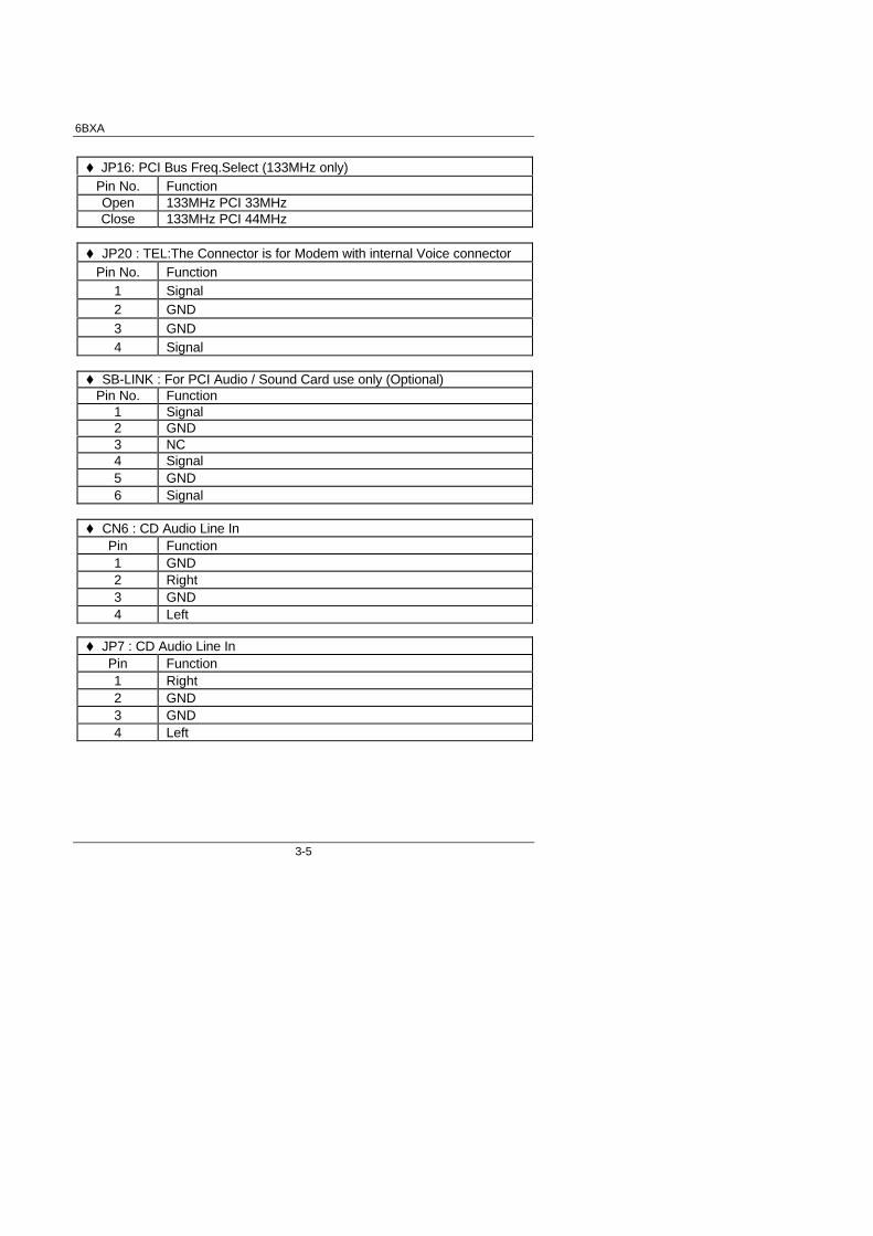
t JP16: PCI Bus Freq.Select (133MHz only)Pin No. FunctionOpen 133MHz PCI 33MHzClose 133MHz PCI 44MHz
t JP20 : TEL:The Connector is for Modem with internal Voice connectorPin No. Function
1 Signal2 GND3 GND4 Signal
t SB-LINK : For PCI Audio / Sound Card use only (Optional)Pin No. Function
1 Signal2 GND3 NC4 Signal5 GND6 Signal
t CN6 : CD Audio Line InPin Function1 GND2 Right3 GND4 Left
t JP7 : CD Audio Line InPin Function1 Right2 GND3 GND4 Left

Hardware Installation
3-6
JP5 : For 2X11 PINs Jumper
PW: Soft Power Connector
Open: Normal OperationShort: Power On/Off
RES: Reset Switch
Open: Normal OperationShort: For Hardware Reset System
P+P−P−: Power LED
PIN 1 : anode (+)PIN 2 : cathode (−)PIN 3 : cathode (−)
SPK: Speaker Connector
PIN 1 : VCCPIN 2 : VCCPIN 3 : DataPIN 4 : Data
HD: IDE Hard Disk Active LED
PIN 1: LED anode (+)PIN 2: LED cathode (−)
GN: Green Function Switch
Open : Normal operationShort : Entering Green Mode
1
1
1
PW P+P−P− HD
RES S P K
GNGD
JP51
1
1
+ −+ −
6BXA
3-7
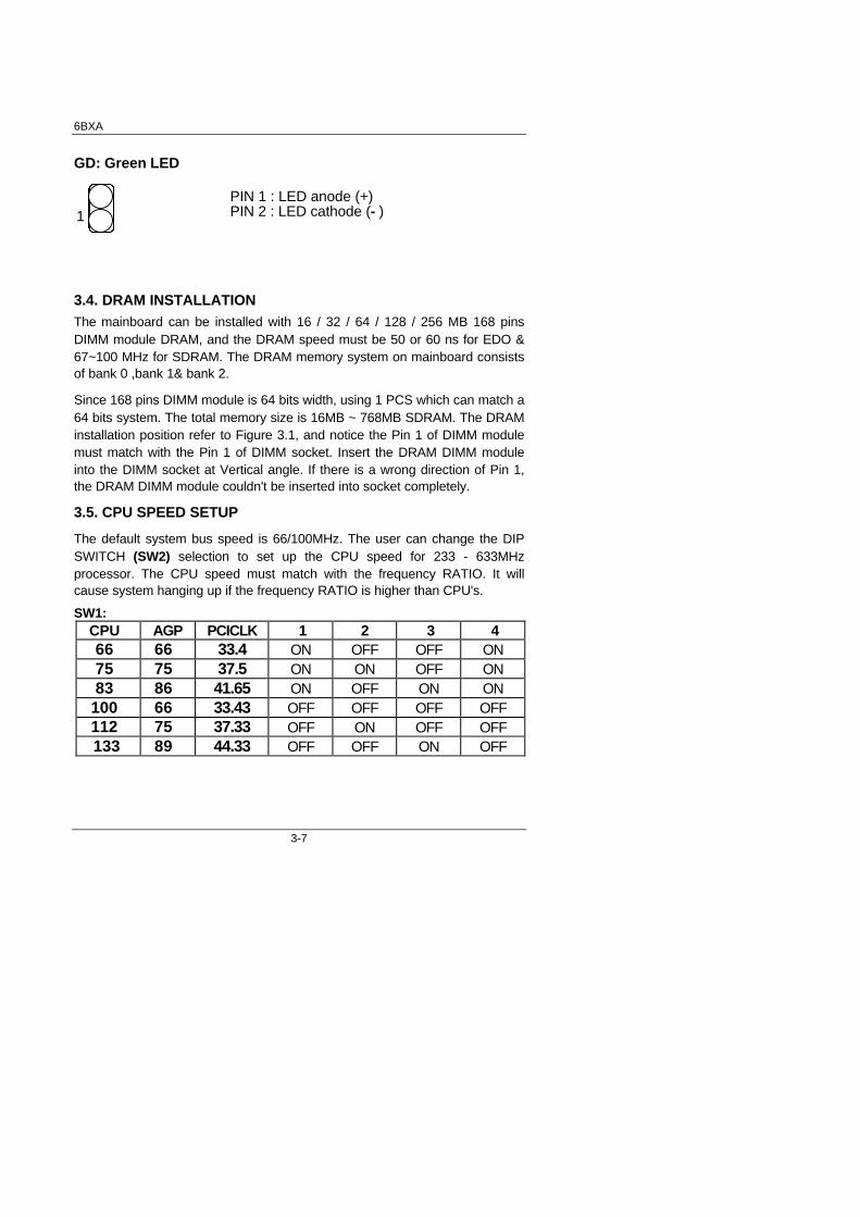
GD: Green LED
PIN 1 : LED anode (+)PIN 2 : LED cathode (−)
3.4. DRAM INSTALLATION
The mainboard can be installed with 16 / 32 / 64 / 128 / 256 MB 168 pinsDIMM module DRAM, and the DRAM speed must be 50 or 60 ns for EDO &67~100 MHz for SDRAM. The DRAM memory system on mainboard consistsof bank 0 ,bank 1& bank 2.
Since 168 pins DIMM module is 64 bits width, using 1 PCS which can match a64 bits system. The total memory size is 16MB ~ 768MB SDRAM. The DRAMinstallation position refer to Figure 3.1, and notice the Pin 1 of DIMM modulemust match with the Pin 1 of DIMM socket. Insert the DRAM DIMM moduleinto the DIMM socket at Vertical angle. If there is a wrong direction of Pin 1,the DRAM DIMM module couldn't be inserted into socket completely.
3.5. CPU SPEED SETUP
The default system bus speed is 66/100MHz. The user can change the DIPSWITCH (SW2) selection to set up the CPU speed for 233 - 633MHzprocessor. The CPU speed must match with the frequency RATIO. It willcause system hanging up if the frequency RATIO is higher than CPU's.
SW1:CPU AGP PCICLK 1 2 3 466 66 33.4 ON OFF OFF ON75 75 37.5 ON ON OFF ON83 86 41.65 ON OFF ON ON
100 66 33.43 OFF OFF OFF OFF112 75 37.33 OFF ON OFF OFF 133 89 44.33 OFF OFF ON OFF
1

Hardware Installation
3-8
SW2:
CLK RATIO 1 2 3 4X3 ON OFF ON ON
X3.5 OFF OFF ON ONX4 ON ON OFF ON
X4.5 OFF ON OFF ONX5 ON OFF OFF ON
X5.5 OFF OFF OFF ONX6 ON ON ON OFF
X6.5 OFF ON ON OFF
MThe CPU is a sensitive electric component and it can be easilydamaged by static electricity, so users must keep it away from metalsurface when the CPU is installed onto mainboard.
MNote: We don’t recommend you to setup your system speed to 75, 83,112 or 133MHz because these frequencies are not the standardspecifications for CPU, Chipset and most of the peripherals.Whether your system can run under 75, 83, 112 or 133MHzproperly will depend on your hardware configurations: CPU,SDRAM, Cards, etc.
3.6. CMOS RTC & ISA CFG CMOS SRAM
The mainboard contains RTC & CMOS SRAM on board. They have a powersupply from external battery to keep the DATA inviolate & effective. The RTCis a REAL-TIME CLOCK device, which provides the DATE & TIME to system.The CMOS SRAM is used for keeping the information of system configuration,so the system can automatically boot OS every time. Since the lifetime ofinternal battery is 5 years, the user can change a new Battery to replace oldone when it has consumed.
3.7. SPEAKER CONNECTOR INSTALLATION
There is a speaker in AT system for sound purpose. The 4 - Pins connectorSPK is used to connect speaker.

6BXA
3-9
3.8. HARDWARE RESET SWITCH CONNECTOR INSTALLATION
The RESET switch on panel provides users with HARDWARE RESETfunction. The system will do a cold start after the RESET switch is press andreleased by user. The RESET switch is a 2 PINS connector and should beinstalled to RES on mainboard.
3.9. POWER LED CONNECTOR INSTALLATION
System has power LED lamp on the panel of case. The power LED will lighton off or flash to indicate which step on the system. The connector should beconnected to LED of mainboard in correct direction.
3.10. IDE & ATAPI DEVICE INSTALLATION
There are two-Enhanced PCI IDE ports (IDE1, IDE2) on board, whichfollowing ATAPI standard SPEC. Any one IDE port can connected to twoATAPI devices (IDE Hard Disk, CD-ROM & Tape Driver), so total four ATAPIdevices can exist in a system. The HD is the active LED port for ATAPIdevices.
3.11. PERIPHERAL DEVICE INSTALLATION
After the I/O device installation and jumpers setup, the mainboard can bemounted into the case and fixed by screw. To complete the mainboardinstallation, the peripheral device could be installed now. The basic systemneeds a display interface card. If the PCI - Bus device is to be installed in thesystem, any one of four PCI - Bus slots can be used.
3.12.PS/2 KEYBOARD & MOUSE INSTALLATION
The main board supports PS/2 Mouse. The BIOS will auto detect whether thePS/2 Mouse is installed or not & assign IRQ12 for PS/2 Mouse port if it isinstalled. After installing the peripheral device, the user should checkeverything again, and prepare to power-on the system.

