systems software & sequential processor
TRANSCRIPT

Sequential Processor
Jin-Soo Kim([email protected])
Systems Software &Architecture Lab.
Seoul National University
Fall 2020
Chap. 4.1 – 4.4

4190.308: Computer Architecture | Fall 2020 | Jin-Soo Kim ([email protected]) 2
▪ CPU performance factors
• Instruction count – Determined by ISA and compiler
• CPI and cycle time – Determined by CPU hardware
▪ We will examine two RISC-V implementations
• A simplified (sequential) version
• A more realistic pipelined version
▪ Simple subset, shows most aspects
• Memory reference: ld, sd
• Arithmetic/logical: add, sub, and, or
• Control transfer: beq

4190.308: Computer Architecture | Fall 2020 | Jin-Soo Kim ([email protected]) 3
▪ Three components required to implement a digital system
• Combinational elements to compute Boolean functions
• Sequential elements to store bits
• Clock signals to regulate the updating of the memory elements
Combinational
elementsOut
Clock
In …
Seq
uen
tiale
lem
en
ts
4190.308: Computer Architecture | Fall 2020 | Jin-Soo Kim ([email protected]) 4
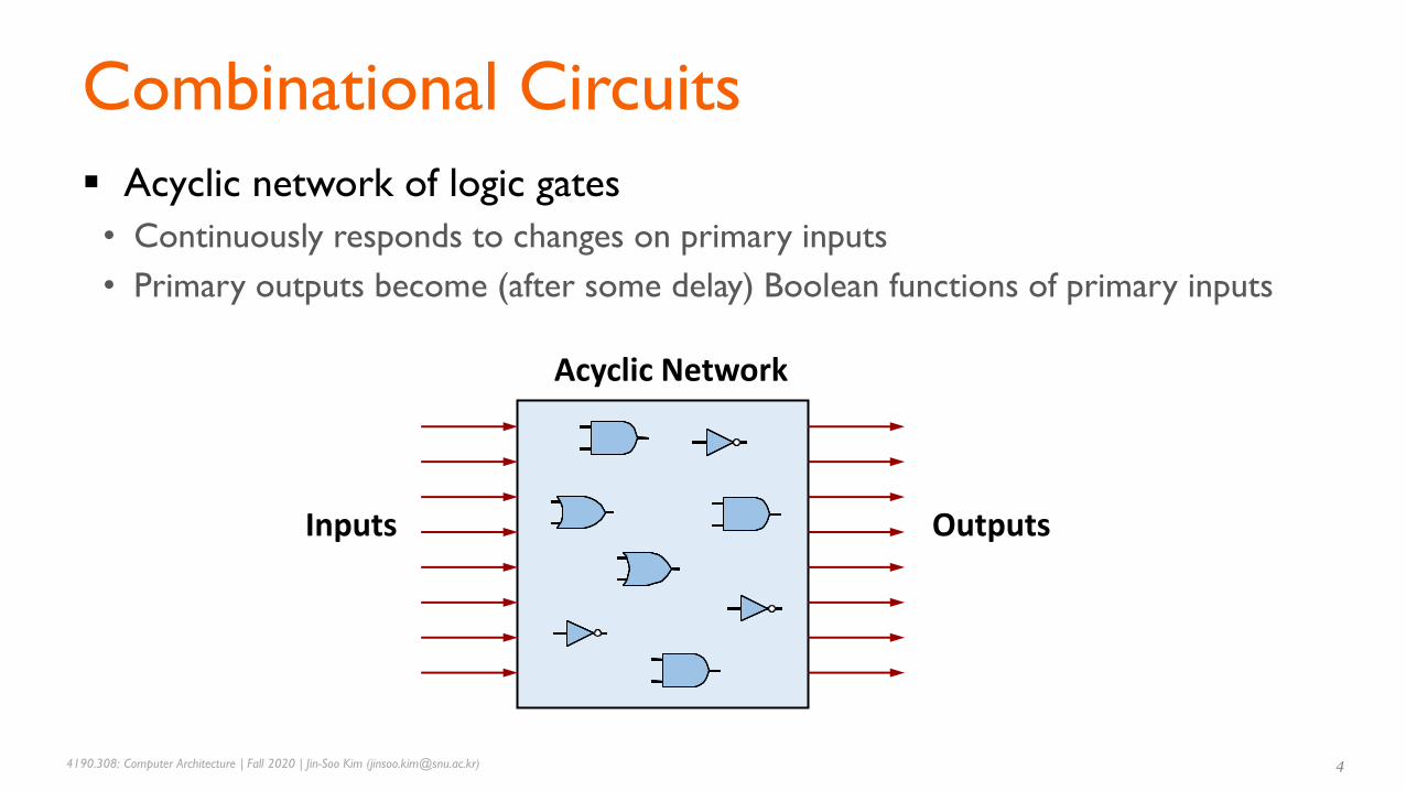
▪ Acyclic network of logic gates
• Continuously responds to changes on primary inputs
• Primary outputs become (after some delay) Boolean functions of primary inputs
Acyclic Network
Inputs Outputs

4190.308: Computer Architecture | Fall 2020 | Jin-Soo Kim ([email protected]) 5
▪ AND-gate
• Y = A & B
▪ Adder
• Y = A + B
▪ Multiplexer
• Y = S? A : B
▪ Arithmetic/Logic Unit
• Y = F(A, B)
AB
Y
A
B
Y+
A
B
YALU
F
AB
Y
S
MUX

4190.308: Computer Architecture | Fall 2020 | Jin-Soo Kim ([email protected]) 6
▪ Register with write control
• Only updates on clock edge when write control input is 1
• Used when stored value is required later
D
Clk
Q
Write
Write
D
Q
Clk
01 1
1 1

4190.308: Computer Architecture | Fall 2020 | Jin-Soo Kim ([email protected]) 7
▪ Stores data bits
▪ For most of time acts as barrier between input and output
▪ As clock rises, loads input
State = x
Risingclock
Output = xInput = y
x
State = y
Output = y
y

4190.308: Computer Architecture | Fall 2020 | Jin-Soo Kim ([email protected]) 8
▪ A collection of registers
• Holds values of “program registers”
• x0 ~ x31 in RISC-V
• Register identifier (5 bits) serves as address
▪ Multiple ports
• Can read and/or write multiple words
in one cycle
• Each has separate address and data input/output
• Data is written to the register
only when RegWrite signal is enabledClock
4190.308: Computer Architecture | Fall 2020 | Jin-Soo Kim ([email protected]) 9
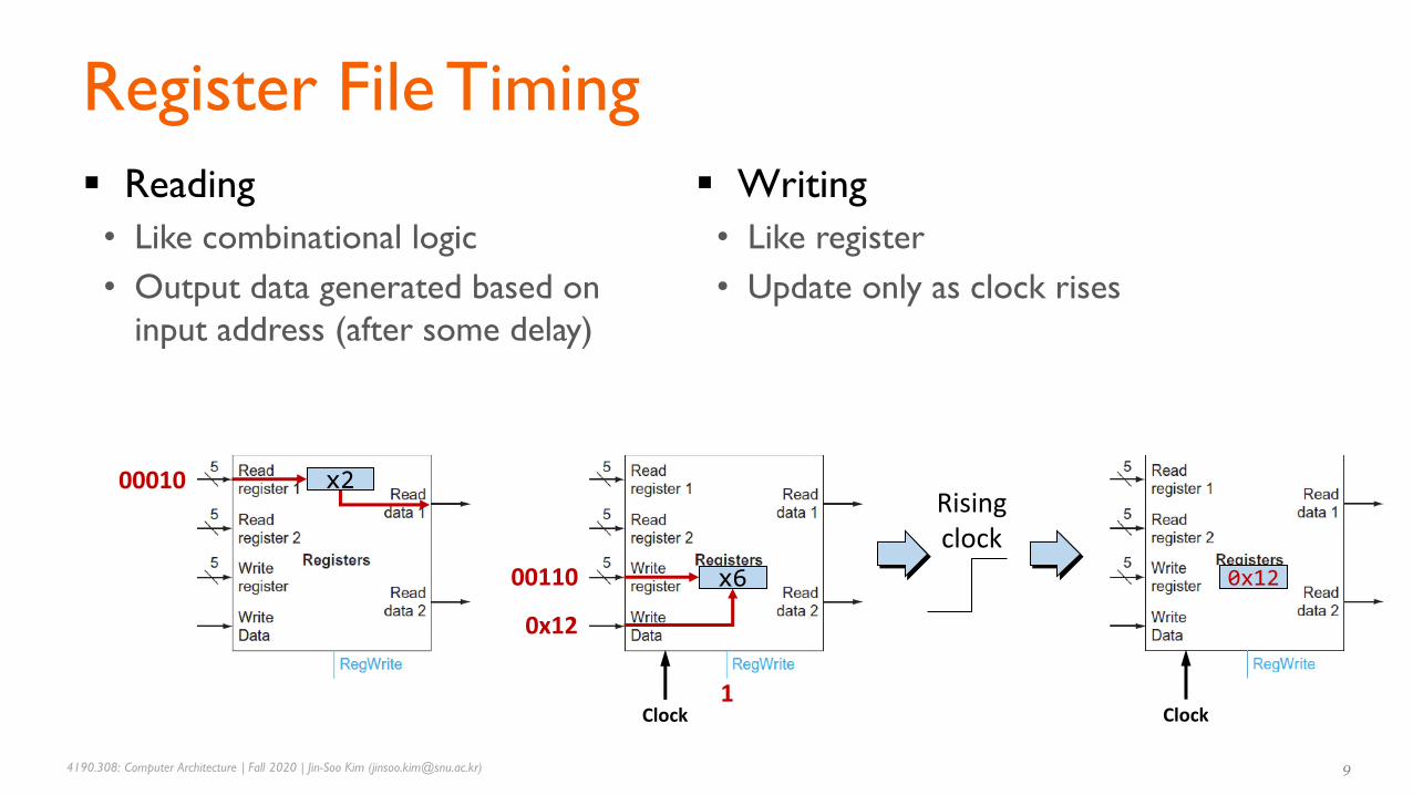
▪ Reading
• Like combinational logic
• Output data generated based on
input address (after some delay)
▪ Writing
• Like register
• Update only as clock rises
x200010
x600110
Clock
0x12
1
Risingclock
0x12
Clock

4190.308: Computer Architecture | Fall 2020 | Jin-Soo Kim ([email protected]) 10
Clock
▪ Random access memory for storing program data
▪ Operations similar to registers
▪ Reading: like combinational logic
▪ Writing: update only as clock rises
▪ Read/Write controlled using MemWrite and
MemRead signals
▪ Another read-only memory needed for instructions
▪ Dual-port memory: single memory for both instructions and data
• One read port for instructions, another read or write port for data

4190.308: Computer Architecture | Fall 2020 | Jin-Soo Kim ([email protected]) 11
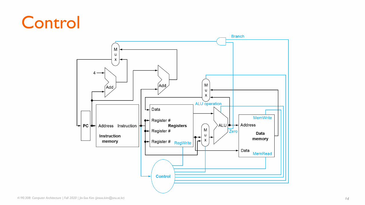
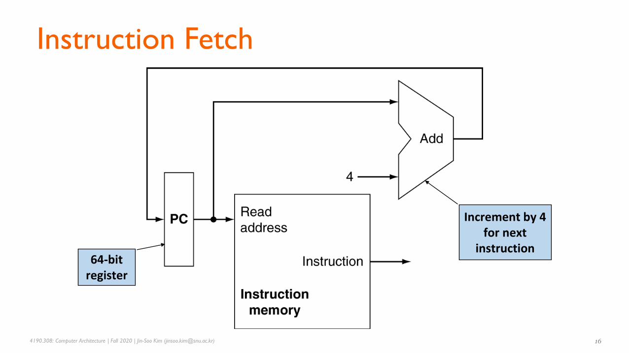
▪ PC → instruction memory, fetch instruction
▪ Register numbers → register file, read registers
▪ Depending on instruction class
• Use ALU to calculate: Arithmetic result
Memory address for load/store
Branch comparison
• Access data memory for load/store
• PC target address or PC + 4
CPU: Datapath + Control

4190.308: Computer Architecture | Fall 2020 | Jin-Soo Kim ([email protected]) 12

4190.308: Computer Architecture | Fall 2020 | Jin-Soo Kim ([email protected]) 13
Can’t just join wires together
→ Use multiplexers
4190.308: Computer Architecture | Fall 2020 | Jin-Soo Kim ([email protected]) 14

4190.308: Computer Architecture | Fall 2020 | Jin-Soo Kim ([email protected]) 15
▪ Datapath
• Elements that process data and addresses in the CPU
• Registers, ALUs, MUX’s, Memories, …
▪ We will build a RISC-V datapath incrementally
• Refining the overview design
4190.308: Computer Architecture | Fall 2020 | Jin-Soo Kim ([email protected]) 16
Increment by 4 for next
instruction64-bit
register

4190.308: Computer Architecture | Fall 2020 | Jin-Soo Kim ([email protected]) 17
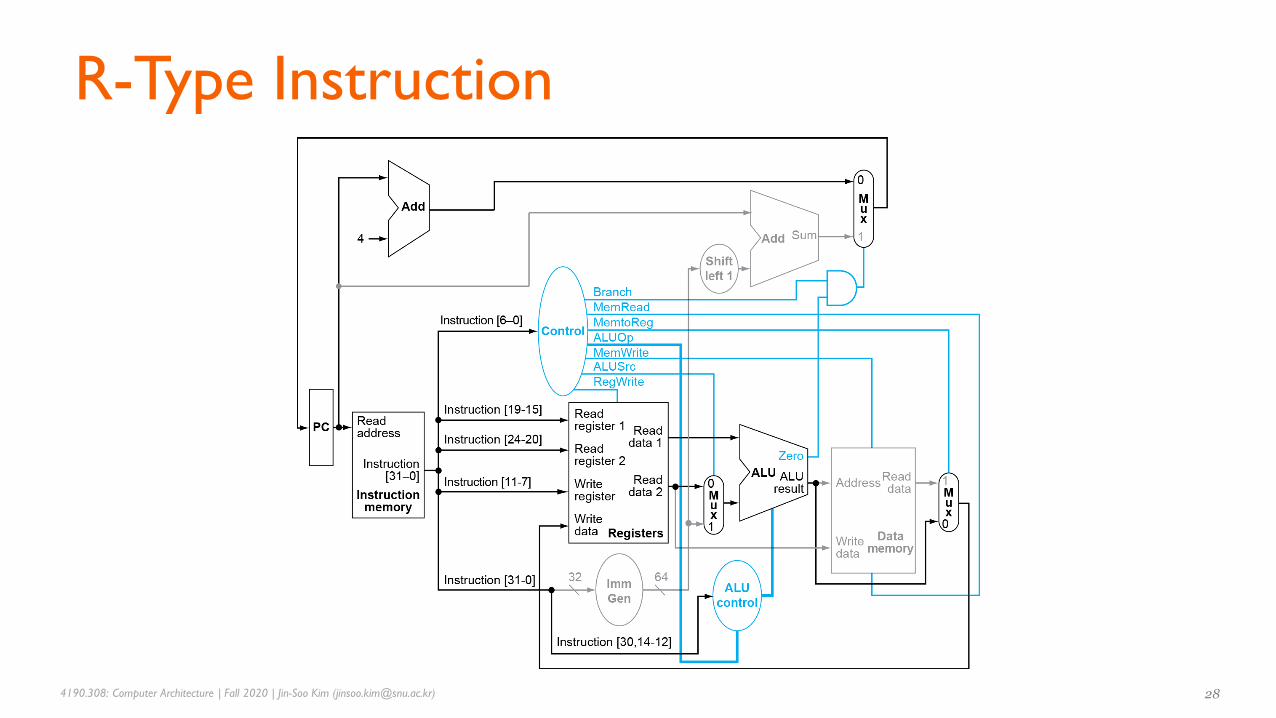
▪ Read two register operands
▪ Perform arithmetic/logical operation
▪ Write register result
4190.308: Computer Architecture | Fall 2020 | Jin-Soo Kim ([email protected]) 18
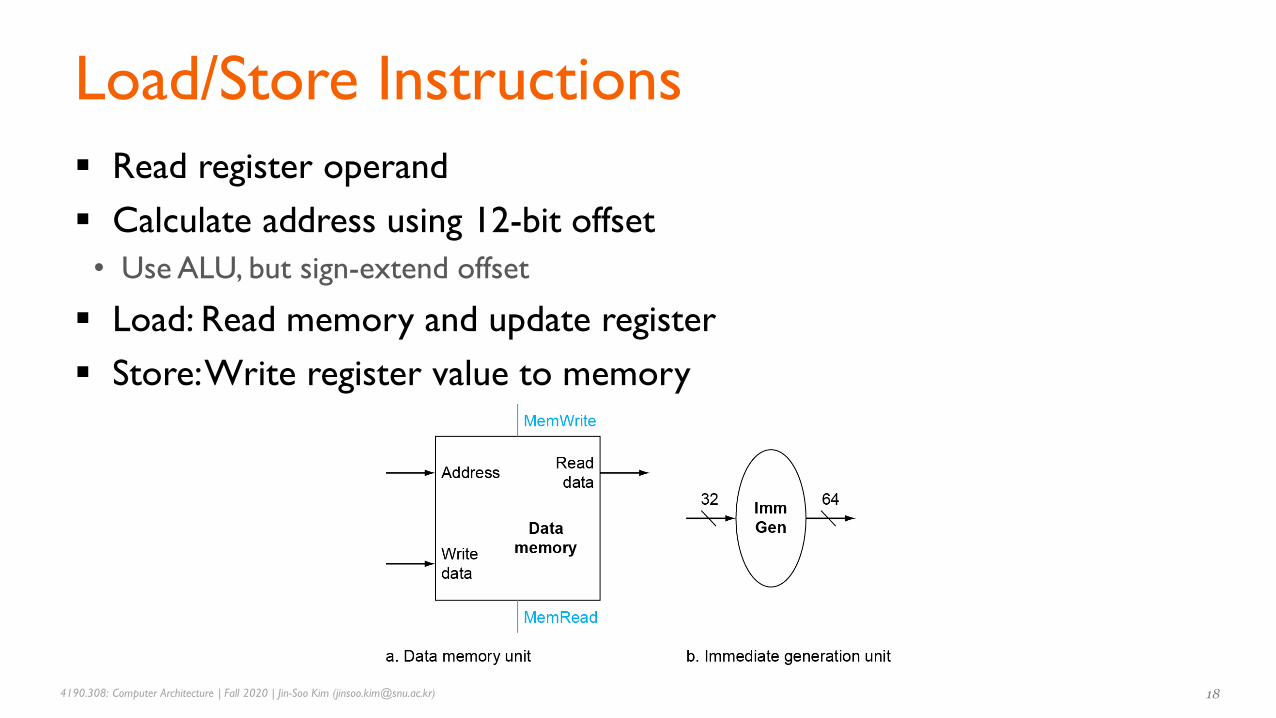
▪ Read register operand
▪ Calculate address using 12-bit offset
• Use ALU, but sign-extend offset
▪ Load: Read memory and update register
▪ Store: Write register value to memory

4190.308: Computer Architecture | Fall 2020 | Jin-Soo Kim ([email protected]) 19
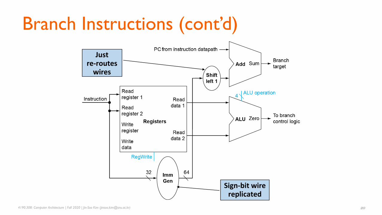
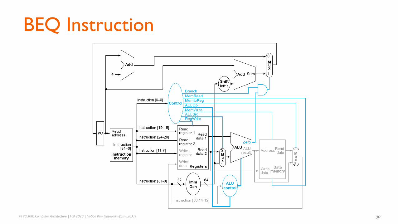
▪ Read register operands
▪ Compare operands
• Use ALU, subtract and check Zero output
▪ Calculate target address
• Sign-extend displacement
• Shift left 1 place (halfword displacement)
• Add to PC value
4190.308: Computer Architecture | Fall 2020 | Jin-Soo Kim ([email protected]) 20
Justre-routes
wires
Sign-bit wire replicated
4190.308: Computer Architecture | Fall 2020 | Jin-Soo Kim ([email protected]) 21
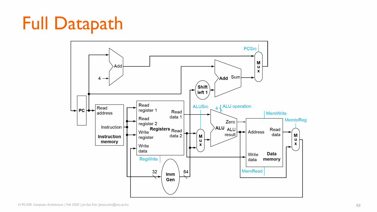
▪ First-cut datapath does an instruction in one clock cycle
• Each datapath element can only do one function at a time
• Hence, we need separate instruction and data memories
▪ Use multiplexers where alternate data sources are used for different
instructions

4190.308: Computer Architecture | Fall 2020 | Jin-Soo Kim ([email protected]) 22
4190.308: Computer Architecture | Fall 2020 | Jin-Soo Kim ([email protected]) 23

4190.308: Computer Architecture | Fall 2020 | Jin-Soo Kim ([email protected]) 24
▪ ALU used for
• Load/Store: F = add
• Branch: F = subtract
• R-type: F depends on opcode
ALU control Function
0000 AND
0001 OR
0010 add
0110 subtract

4190.308: Computer Architecture | Fall 2020 | Jin-Soo Kim ([email protected]) 25
▪ Assume 2-bit ALUOp derived from opcode
• Combinational logic derives ALU control
opcode ALUOp Operation funct7 funct3ALU
functionALU
control
ld 00 load register XXXXXXX XXX add 0010
sd 00 store register XXXXXXX XXX add 0010
beq 01 branch on equal XXXXXXX XXX subtract 0110
R-type 10
add 0000000 000 add 0010
subtract 0100000 000 subtract 0110
AND 0000000 111 AND 0000
OR 0000000 110 OR 0001

4190.308: Computer Architecture | Fall 2020 | Jin-Soo Kim ([email protected]) 26
▪ Control signals derived from instruction
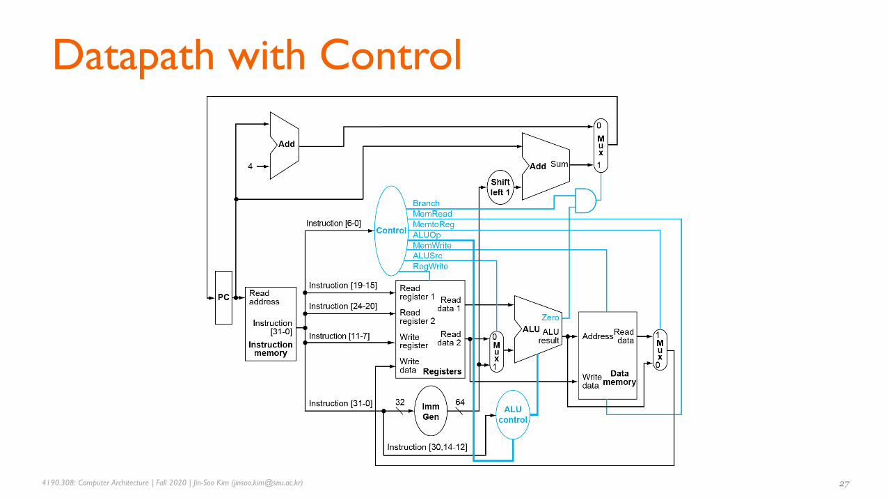
4190.308: Computer Architecture | Fall 2020 | Jin-Soo Kim ([email protected]) 27
4190.308: Computer Architecture | Fall 2020 | Jin-Soo Kim ([email protected]) 28

4190.308: Computer Architecture | Fall 2020 | Jin-Soo Kim ([email protected]) 29
4190.308: Computer Architecture | Fall 2020 | Jin-Soo Kim ([email protected]) 30

4190.308: Computer Architecture | Fall 2020 | Jin-Soo Kim ([email protected]) 31
▪ Longest delay determines clock period
• Critical path: load instruction
• Instruction memory → register file →ALU → data memory → register file
▪ Not feasible to vary period for different instructions
▪ Violates design principle: Making the common case fast
▪ We will improve performance by pipelining

SNURISC-SEQ
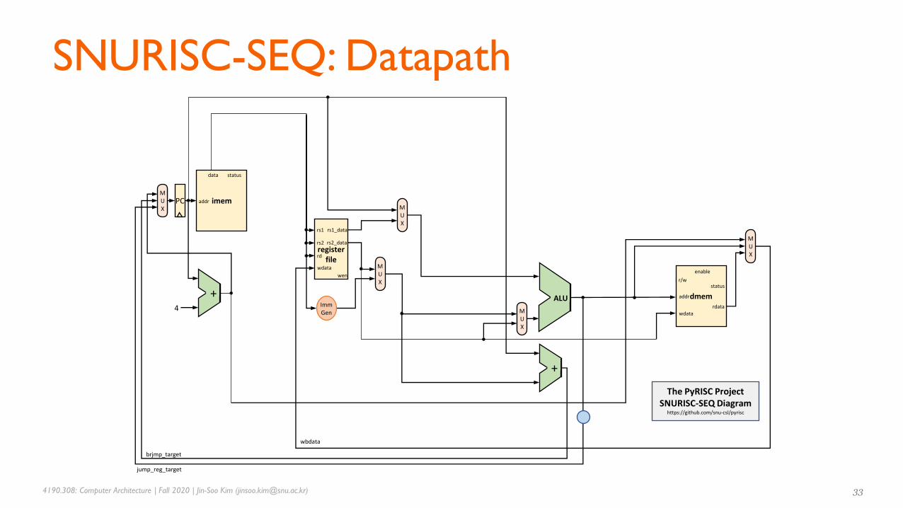
4190.308: Computer Architecture | Fall 2020 | Jin-Soo Kim ([email protected]) 33
registerfile
PC imem
4
MUX
MUX
ALU
+
+
brjmp_target
jump_reg_target
addr
data status
wbdata
rs1
rs2
wdata
rs1_data
rs2_data
The PyRISC ProjectSNURISC-SEQ Diagram
https://github.com/snu-csl/pyrisc
MUX
MUX
wen
rd
dmem
enable
status
rdata
r/w
addr
wdataMUX
ImmGen

4190.308: Computer Architecture | Fall 2020 | Jin-Soo Kim ([email protected]) 34
registerfile
Control
PC imem
4
MUX
MUX
ALU
+
+
brjmp_target
jump_reg_target
addr
data status
wbdatarf_wen
rs1
rs2
wdata
rs1_data
rs2_data
op2_sel
op1_sel
pc_sel
The PyRISC ProjectSNURISC-SEQ Diagram
https://github.com/snu-csl/pyrisc
MUX wb_sel
alu_fun
dmem_valid
dmem_fcn
MUX
wen
rd
exception
dmem
enable
status
rdata
r/w
addr
wdataMUX
br_type
ImmGen
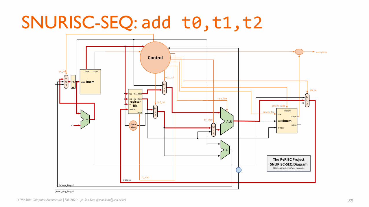
4190.308: Computer Architecture | Fall 2020 | Jin-Soo Kim ([email protected]) 35
registerfile
Control
PC imem
4
MUX
MUX
ALU
+
+
brjmp_target
jump_reg_target
addr
data status
wbdatarf_wen
rs1
rs2
wdata
rs1_data
rs2_data
op2_sel
op1_sel
pc_sel
The PyRISC ProjectSNURISC-SEQ Diagram
https://github.com/snu-csl/pyrisc
MUX wb_sel
alu_fun
dmem_valid
dmem_fcn
MUX
wen
rd
exception
dmem
enable
status
rdata
r/w
addr
wdataMUX
br_type
ImmGen

4190.308: Computer Architecture | Fall 2020 | Jin-Soo Kim ([email protected]) 36
registerfile
Control
PC imem
4
MUX
MUX
ALU
+
+
brjmp_target
jump_reg_target
addr
data status
wbdatarf_wen
rs1
rs2
wdata
rs1_data
rs2_data
op2_sel
op1_sel
pc_sel
The PyRISC ProjectSNURISC-SEQ Diagram
https://github.com/snu-csl/pyrisc
MUX wb_sel
alu_fun
dmem_valid
dmem_fcn
MUX
wen
rd
exception
dmem
enable
status
rdata
r/w
addr
wdataMUX
br_type
ImmGen

4190.308: Computer Architecture | Fall 2020 | Jin-Soo Kim ([email protected]) 37
registerfile
Control
PC imem
4
MUX
MUX
ALU
+
+
brjmp_target
jump_reg_target
addr
data status
wbdatarf_wen
rs1
rs2
wdata
rs1_data
rs2_data
op2_sel
op1_sel
pc_sel
The PyRISC ProjectSNURISC-SEQ Diagram
https://github.com/snu-csl/pyrisc
MUX wb_sel
alu_fun
dmem_valid
dmem_fcn
MUX
wen
rd
exception
dmem
enable
status
rdata
r/w
addr
wdataMUX
br_type
ImmGen
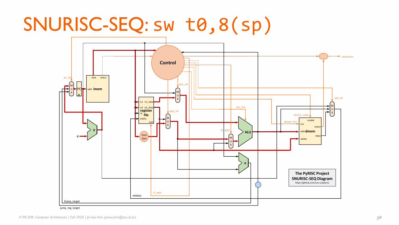
4190.308: Computer Architecture | Fall 2020 | Jin-Soo Kim ([email protected]) 38
registerfile
Control
PC imem
4
MUX
MUX
ALU
+
+
brjmp_target
jump_reg_target
addr
data status
wbdatarf_wen
rs1
rs2
wdata
rs1_data
rs2_data
op2_sel
op1_sel
pc_sel
The PyRISC ProjectSNURISC-SEQ Diagram
https://github.com/snu-csl/pyrisc
MUX wb_sel
alu_fun
dmem_valid
dmem_fcn
MUX
wen
rd
exception
dmem
enable
status
rdata
r/w
addr
wdataMUX
br_type
ImmGen
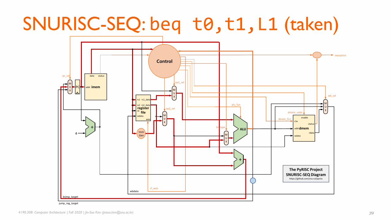
4190.308: Computer Architecture | Fall 2020 | Jin-Soo Kim ([email protected]) 39
registerfile
Control
PC imem
4
MUX
MUX
ALU
+
+
brjmp_target
jump_reg_target
addr
data status
wbdatarf_wen
rs1
rs2
wdata
rs1_data
rs2_data
op2_sel
op1_sel
pc_sel
The PyRISC ProjectSNURISC-SEQ Diagram
https://github.com/snu-csl/pyrisc
MUX wb_sel
alu_fun
dmem_valid
dmem_fcn
MUX
wen
rd
exception
dmem
enable
status
rdata
r/w
addr
wdataMUX
br_type
ImmGen
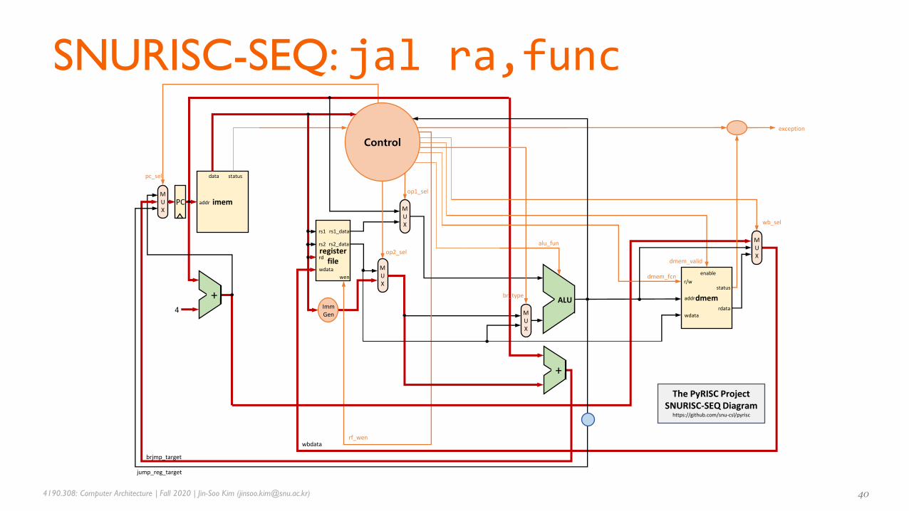
4190.308: Computer Architecture | Fall 2020 | Jin-Soo Kim ([email protected]) 40
registerfile
Control
PC imem
4
MUX
MUX
ALU
+
+
brjmp_target
jump_reg_target
addr
data status
wbdatarf_wen
rs1
rs2
wdata
rs1_data
rs2_data
op2_sel
op1_sel
pc_sel
The PyRISC ProjectSNURISC-SEQ Diagram
https://github.com/snu-csl/pyrisc
MUX wb_sel
alu_fun
dmem_valid
dmem_fcn
MUX
wen
rd
exception
dmem
enable
status
rdata
r/w
addr
wdataMUX
br_type
ImmGen

4190.308: Computer Architecture | Fall 2020 | Jin-Soo Kim ([email protected]) 41
registerfile
Control
PC imem
4
MUX
MUX
ALU
+
+
brjmp_target
jump_reg_target
addr
data status
wbdatarf_wen
rs1
rs2
wdata
rs1_data
rs2_data
op2_sel
op1_sel
pc_sel
The PyRISC ProjectSNURISC-SEQ Diagram
https://github.com/snu-csl/pyrisc
MUX wb_sel
alu_fun
dmem_valid
dmem_fcn
MUX
wen
rd
exception
dmem
enable
status
rdata
r/w
addr
wdataMUX
br_type
ImmGen