system-in-package research within the · pdf filesystem-in-package research within the iemrc...
TRANSCRIPT

System-in-Package Research within the IeMRC
Prof. Andrew RichardsonLancaster University
Contributions from Chris Bailey, Changhai Wang & Jean Marc Yannou (NXP)
LANCASTERU N I V E R S I T YCentre for Microsystems EngineeringFaculty of Applied Sciences
LANCASTERU N I V E R S I T YCentre for Microsystems EngineeringFaculty of Applied Sciences

Outline
•
IeMRC
System-in-Package Projects•
Partner Profiles
•
Introduction to SiP
and Challenges (NXP example)
•
IeMRC
Research–
Introduction to reliability modelling (extended by Stoyan)
–
Health Monitoring & Embedded Test

Project Statistics
•
Design for Manufacture Methodology for SiP–
Academic partners : Lancaster University & Greenwich
–
Industrial partners : NXP, Flowmerics, Coventor
& Selex–
£206K –
Nov 2005 –
Nov 2007
–
Focus : Reliability Engineering of SiP
assemblies
•
Integrated Health Monitoring of MNT Enabled Integrated Systems “I-Health”–
Academic partners : Lancaster University & Heriot
Watt
University–
Industrial partners : NXP, QinetiQ, Coventor, MCE
–
Focus : Embedded Test & Health Monitoring of SiP
based systems

SiP-Design
•
Design for Manufacture Methodology for SiP–
Realise algorithms and associated code to generate an integral thermal map across a behavioural model of an SiP
structure.
–
Realise algorithms and associated code to model and couple electromagnetic and electrostatic fields into functional devices and materials within an SiP
structure.–
Realise a method of injecting defects and degradation into structural SiP
models. Address the test issue.
–
Demonstrate the above advances in an industrial virtual prototype environment
“I-Health”
project SP/05/01/03
•
Integrated Health Monitoring of MNT Enabled Integrated Systems–
The potential to realise low cost temperature, stress, humidity and EM field sensors for integration in a health monitoring architecture.
–
Electrical only strategies that requires low performance electronics to monitor non-electrical functions both on-line and in production.
–
A solution for embedding both sensing and electrical monitoring functions within a SiP
level test access and control architecture
together with decision making functions based on re-use and / or reconfiguration of existing functions and both fault tolerance and self-
repair through redundancy and emulation.–
Implementation solutions including on-chip, on-substrate and through dedicated low cost health inserts for both silicon and LTCC platforms.

University of Greenwich
•
Centre for Numerical Modelling and Process Analysis–
5 Profs, 20+ Post Docs, 40 + PhD’s
–
One of largest groups in UK•
Electronics and Microsystems –
2 Profs, 4 Post Doc’s, 10 PhD’s
–
Over £4m of support since 1998 in electronics and microsystems modelling.
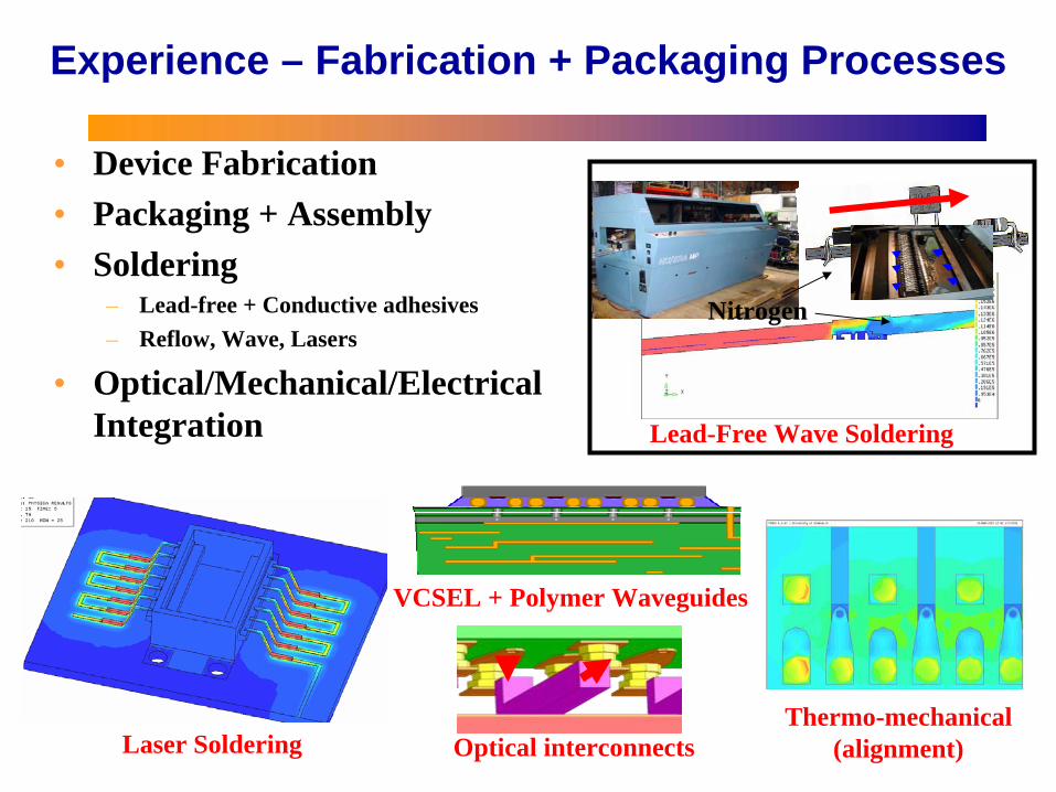
Experience – Fabrication + Packaging Processes
•
Device Fabrication•
Packaging + Assembly
•
Soldering–
Lead-free + Conductive adhesives–
Reflow, Wave, Lasers
•
Optical/Mechanical/Electrical Integration
Nitrogen
Lead-Free Wave Soldering
VCSEL + Polymer Waveguides
Optical interconnectsThermo-mechanical
(alignment)Laser Soldering
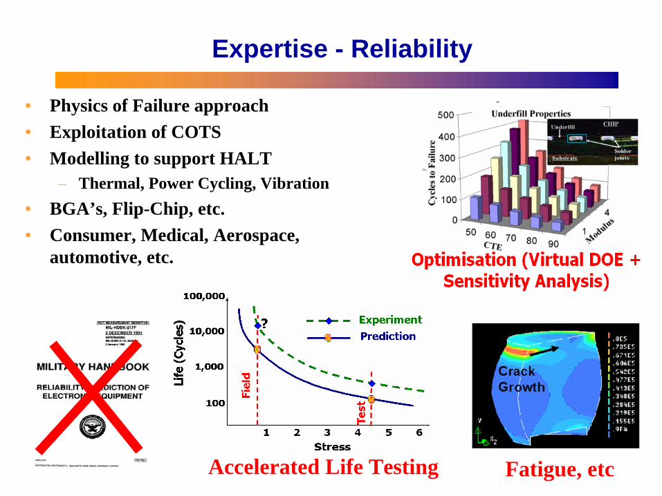
Expertise - Reliability
•
Physics of Failure approach•
Exploitation of COTS
•
Modelling to support HALT–
Thermal, Power Cycling, Vibration
•
BGA’s, Flip-Chip, etc.•
Consumer, Medical, Aerospace, automotive, etc.
Accelerated Life Testing Fatigue, etc

Lancaster University
•
Centre for Microsystems Engineering–
4 academic staff, 5 RA’s, 4 PhD’s
–
Delivered against £3.4M in grant income over the past 10 years
–
Leads the European Design for Micro & Nano Manufacture community through the FP6 Network of Excellence (PATENT-DfMM)

Research, training and industrial services in the Engineering ScResearch, training and industrial services in the Engineering Science ience associated with Design for Manufacture Technology for Micro & associated with Design for Manufacture Technology for Micro & NanoNano
Technology based ProductsTechnology based Products
Key SkillsDesign methodology, modelling & simulation of MNT based structures and systems.Fault tolerant design, design for test, condition monitoring and test engineering for MNT based systems.Integration technology for MNT based systems (packaging)
Active ProjectsEU FP6 “INTEGRAMplus" Integrated MNT Platforms & Services (IP), “PATENT-DfMM” Design for Micro & Nano Manufacture (NoE) and “MINOS-EURONET”Micro-Nanosystems European Network pursuing the integration of NMS and ACC in ERA.
EPSRC "Nanoelectronics”: Nanoelectronic Device Modelling for System Design " 2006 – 2009 and IeMRC projects SiP-Design and I-Health.HEIF / NWDA Science & Entrepreneurship training award in MNT
Centre for Microsystems Engineering - Mission
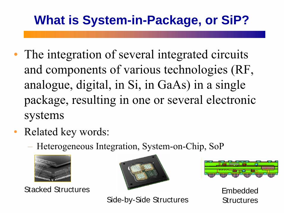
What is System-in-Package, or SiP?
•
The integration of several integrated circuits and components of various technologies (RF, analogue, digital, in Si, in GaAs) in a single package, resulting in one or several electronic systems
•
Related key words:–
Heterogeneous Integration, System-on-Chip, SoP
Stacked StructuresSide-by-Side Structures
Embedded Structures
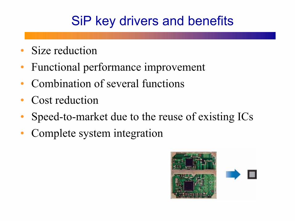
SiP key drivers and benefits
•
Size reduction•
Functional performance improvement
•
Combination of several functions•
Cost reduction
•
Speed-to-market due to the reuse of existing ICs•
Complete system integration
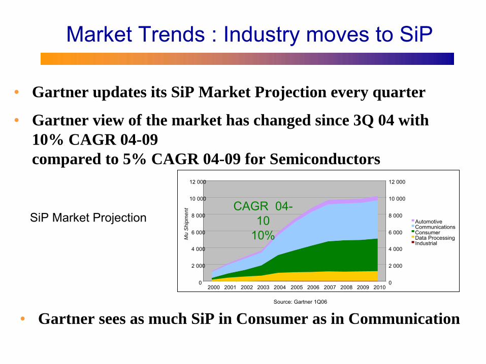
Market Trends : Industry moves to SiP
•
Gartner updates its SiP Market Projection every quarter
•
Gartner view of the market has changed since 3Q 04 with 10% CAGR 04-09 compared to 5% CAGR 04-09 for Semiconductors
SiP Market Projection
0
2 000
4 000
6 000
8 000
10 000
12 000
2000 2001 2002 2003 2004 2005 2006 2007 2008 2009 2010
Mu
Shi
pmen
t
0
2 000
4 000
6 000
8 000
10 000
12 000
AutomotiveCommunicationsConsumerData ProcessingIndustrial
Source: Gartner 1Q06
CAGR 04- 10
10%
•
Gartner sees as much SiP in Consumer as in Communication
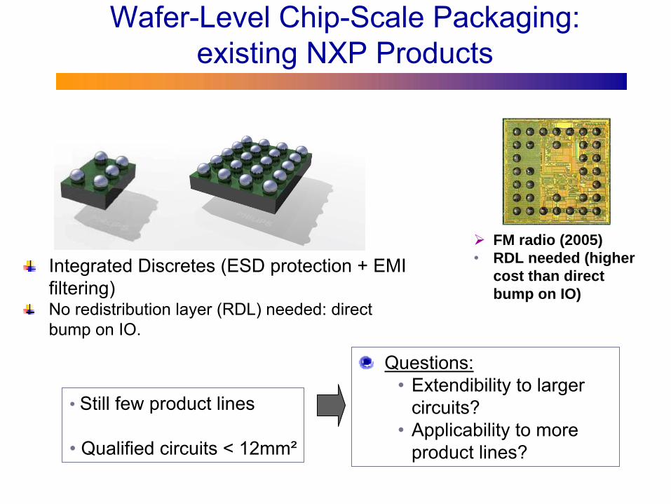
Wafer-Level Chip-Scale Packaging: existing NXP Products
Integrated Discretes
(ESD protection + EMI filtering)No redistribution layer (RDL) needed: direct bump on IO.
FM radio (2005)•
RDL needed (higher cost than direct bump on IO)
• Still few product lines
• Qualified circuits < 12mm²
Questions:•
Extendibility to larger circuits?
•
Applicability to more product lines?

Market Trends : Industry moves to WLP
•
Both TechSearch
and Gartner confirms a significant growth of WLP deliveries
•
70% of WLP applied to Integrated Passives in 2005
Source: Gartner 1Q06 + TechSearch
3Q04
WLP Market Projection
0
2 000
4 000
6 000
8 000
10 000
12 000
14 000
16 000
18 000
2000 2001 2002 2003 2004 2005 2006 2007 2008 2009 2010
Mu
ship
men
t
Gartner
TechSearchGartner 1Q06
CAGR 04-0933%
TechSearch 4Q04CAGR 04-09
26%
•
Expected CAGR 04- 09 > 25%
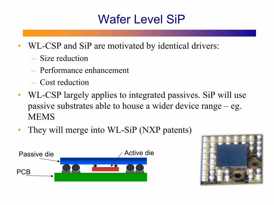
Wafer Level SiP
•
WL-CSP and SiP are motivated by identical drivers:–
Size reduction
–
Performance enhancement–
Cost reduction
•
WL-CSP largely applies to integrated passives. SiP will use passive substrates able to house a wider device range –
eg.
MEMS•
They will merge into WL-SiP (NXP patents)
Q i
d d f h i d ?
PCB
Passive die Active die
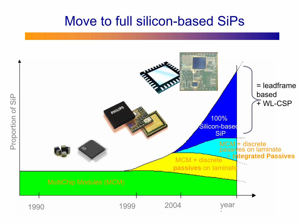
Move to full silicon-based SiPs
year
MCM + discretepassives on laminate
MCM + discretepassives on laminate+ Integrated Passive
Multi-Chip Modules (MCM)
100%silicon-based
SiP
1990 1999 2004
Pro
porti
on o
f SiP
year
MCM + discretepassives on laminate
MCM + discretepassives on laminate
+ Integrated Passives
MultiChip
Modules (MCM)
100%Silicon-based
SiP
1990 1999 2004
= leadframe based
+ WL-CSP

Integration Trend
Passive/Interconnect dieActive Die
SMDs
/ Components
Discretes
SolutionsPCB
MCM SolutionsPCB
Laminate + SMDs
SolutionsPCB
Laminate + SMDs
+ Passive diePCB
Double Flip Chip assemblyPCB
Wafer Level PackagingPCB
3D WLP SiPsPCB
NXP SiP Platforms Trend
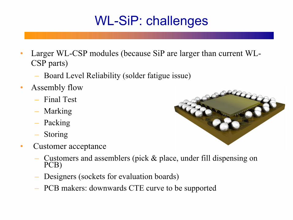
WL-SiP: challenges
•
Larger WL-CSP modules (because SiP are larger than current WL- CSP parts)
–
Board Level Reliability
(solder fatigue issue)•
Assembly flow–
Final Test
–
Marking–
Packing
–
Storing•
Customer acceptance–
Customers and assemblers (pick & place, under fill dispensing on
PCB)–
Designers (sockets for evaluation boards)
–
PCB makers: downwards CTE curve to be supported

Number of TMC cycles
% u
nits
faili
ng
Improved Si technologies, lower PCB CTE’s
Larger WLP modules
Board Level Reliability: solder fatigue (1)
•
Visible by thermal cycling
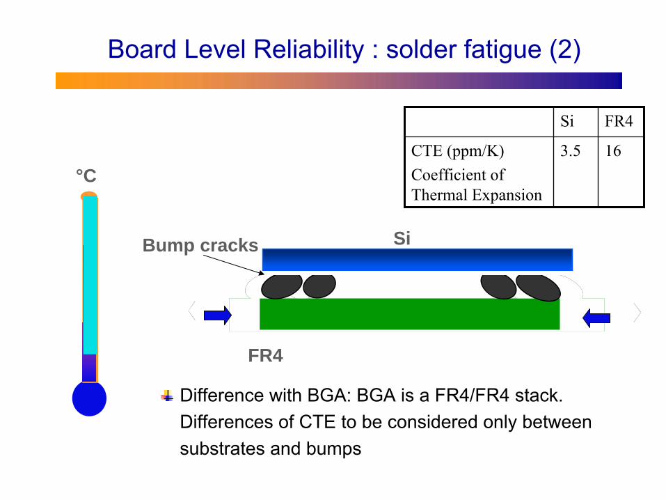
Board Level Reliability : solder fatigue (2)
FR4
Si
°C
Bump cracks
Si FR4
CTE (ppm/K)Coefficient of Thermal Expansion
3.5 16
Difference with BGA: BGA is a FR4/FR4 stack. Differences of CTE to be considered only between substrates and bumps

Simulation and Modelling
Requirements
•
Accurate simulation and modelling
is useful–
In the short term
•
To assess reliability of current WL-CSP technologies with respect to larger sizes
•
To compare possible technology options–
New materials (underfills, bump alloys, PCB’s)
–
New balling layout rules
–
In the longer term•
To “virtually qualify”
WL-CSP parts:
–
How to make sure a new product has every chance to first time pass qualification stresses according to the company specific General Quality System?
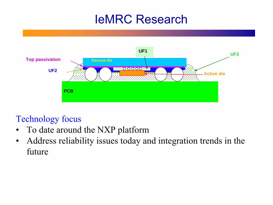
IeMRC Research
UF2
PCB
Passive die
Active die
UF3UF1
Top passivation
Technology focus•
To date around the NXP platform
•
Address reliability issues today and integration trends in the future
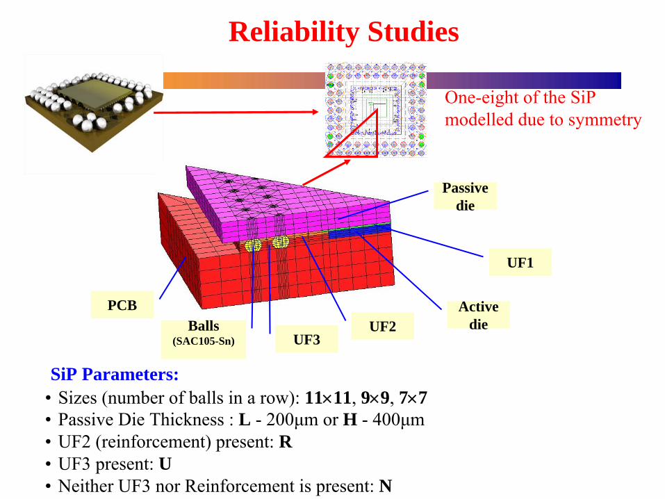
Reliability Studies
SiP Parameters:•
Sizes (number of balls in a row): 11×11, 9×9,
7×7
•
Passive Die Thickness : L -
200μm or H - 400μm•
UF2 (reinforcement) present: R
•
UF3 present: U •
Neither UF3 nor Reinforcement is present: N
One-eight of the SiP modelled due to symmetry
PCBBalls
(SAC105-Sn)
Passive die
Active dieUF2
UF3
UF1

Plan of ExperimentsTest Size UF Passive die
thickness11HR 11×11 UF2 40011LR 11×11 UF2 20011HU 11×11 UF3 40011LU 11×11 UF3 20011HN 11×11 None 40011LN 11×11 None 200
Test Size UF Passive die
09HR 9×9 UF2 400
09LR 9×9 UF2 200
09HU 9×9 UF3 400
09LU 9×9 UF3 200
09HN 9×9 None 400
09LN 9×9 None 200
Test Size UF Passive die thickness
07HR 7×7 UF2 40007LR 7×7 UF2 20007HU 7×7 UF3 40007LU 7×7 UF3 20007HN 7×7 None 40007LN 7×7 None 200
Assume a stress-free state at 125ºC
-40°C
125°C
45min
15min
105min
60min
120min
Thermal Cycling Profile
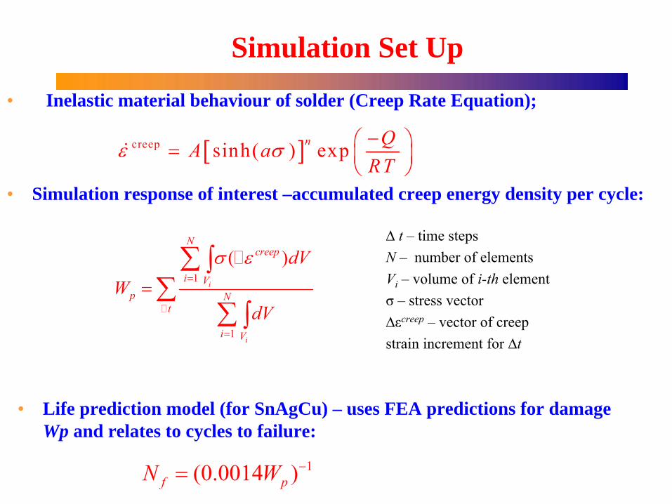
Simulation Set Up
[ ]creep sinh( ) expn QA aRT
ε σ −⎛ ⎞= ⎜ ⎟⎝ ⎠
&
•
Inelastic material behaviour of solder (Creep Rate Equation);
•
Simulation response of interest –accumulated creep energy density per cycle:
1
1
( )i
i
Ncreep
i Vp N
t
i V
dVW
dV
σ ε=
=
=∑∫
∑∑∫
∆
t – time stepsN –
number of elementsVi
–
volume of
i-th
elementσ
–
stress vector∆εcreep
–
vector of creep strain increment for ∆t
•
Life prediction model (for SnAgCu) – uses FEA predictions for damage Wp and relates to cycles to failure:
1(0.0014 )f pN W −=
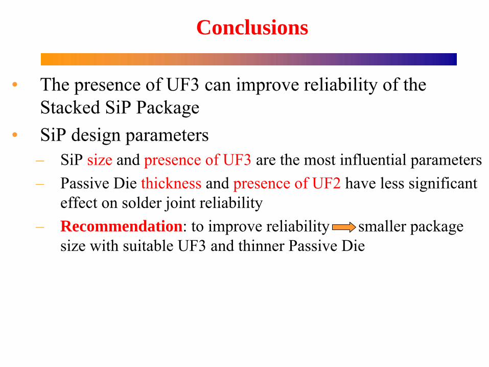
Conclusions
•
The presence of UF3 can improve reliability of the Stacked SiP Package
•
SiP design parameters–
SiP size
and presence of UF3
are the most influential parameters
–
Passive Die thickness
and presence of UF2
have less significant effect on solder joint reliability
–
Recommendation: to improve reliability smaller package size with suitable UF3 and thinner Passive Die

Carrier substrate
Active: Health monitor central unit
EMI probeTemperature sensor
Passives: test response read out & stimulus injection
MEMS
Health Monitoring –
embedded concept
- Integrated sensors: temperature, EMI probes etc…
- MEMS testing
- System reconfiguration
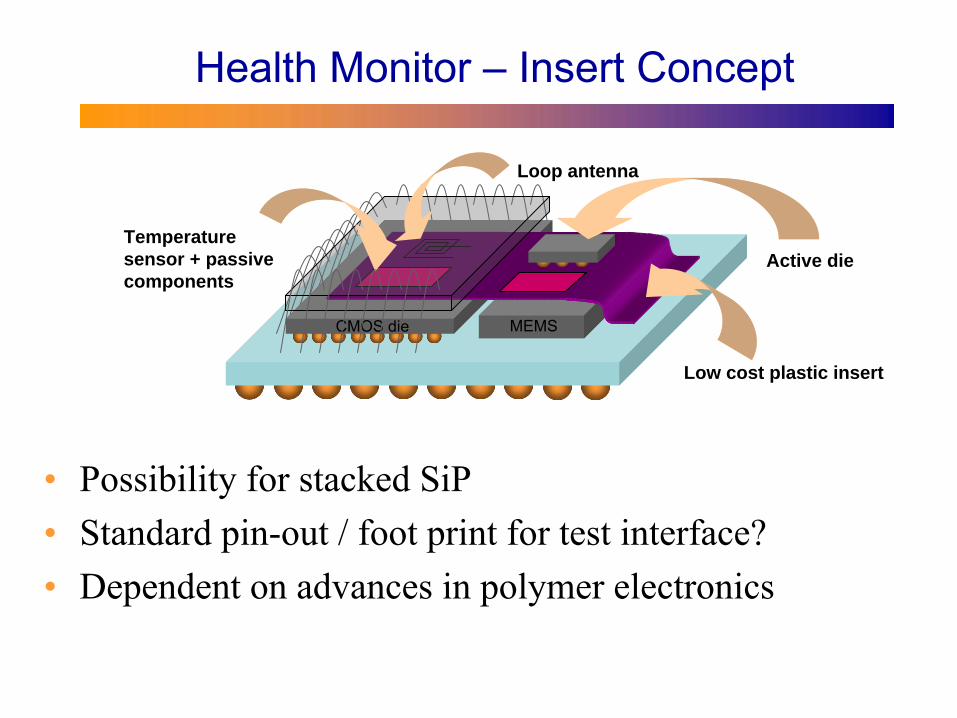
Health Monitor –
Insert Concept
•
Possibility for stacked SiP•
Standard pin-out / foot print for test interface?
•
Dependent on advances in polymer electronics
CMOS die MEMS
Loop antenna
Temperature sensor + passive components
Active die
Low cost plastic insert
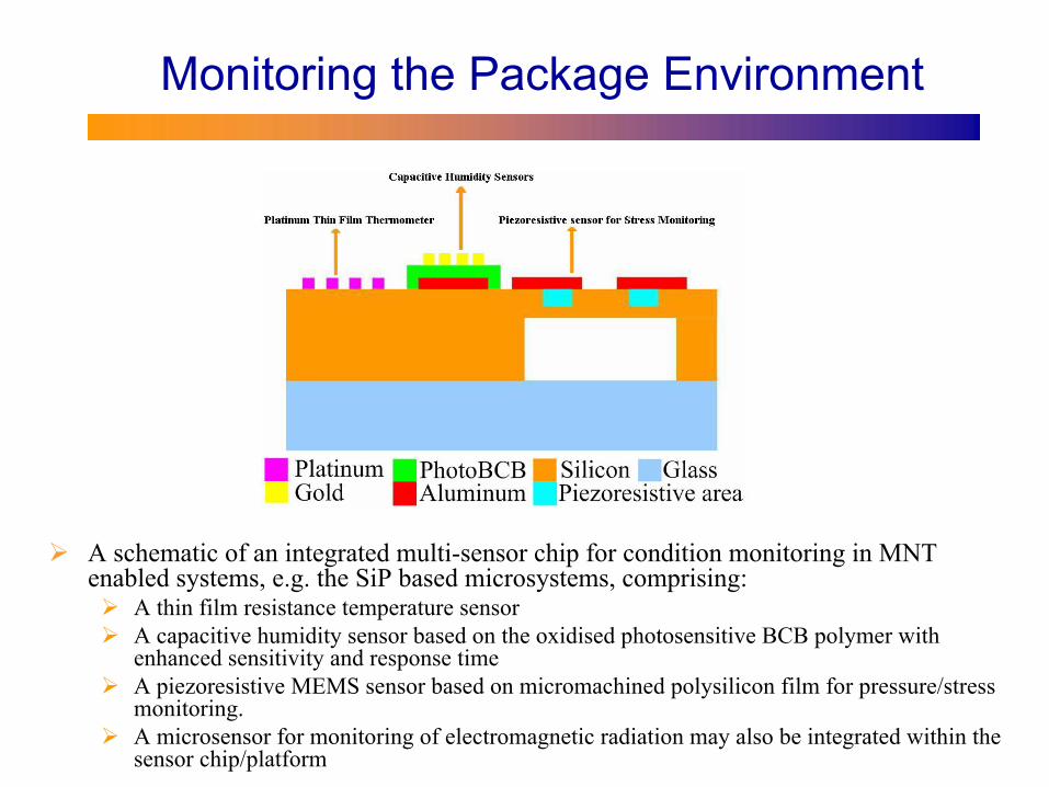
Monitoring the Package Environment
A schematic of an integrated multi-sensor chip for condition monitoring in MNT enabled systems, e.g. the SiP based microsystems, comprising:
A thin film resistance temperature sensorA capacitive humidity sensor based on the oxidised photosensitive BCB polymer with enhanced sensitivity and response timeA piezoresistive MEMS sensor based on micromachined polysilicon film for pressure/stress monitoring. A microsensor for monitoring of electromagnetic radiation may also be integrated within the sensor chip/platform

Platinum Thin Film Resistance Thermometer
–
The thin film resistance thermometer:
•
Temperature range: -200ºC ~ 1000ºC
•
Advantages: Accurate, stable. •
Disadvantages: Self-heating, nonlinear response.

Non-electrical functions –
bias superposition
Feasibility on magnetometer, accelerometer, conductance sensor
•
Electrical only test & monitoring techniques for MNT systems
TranducerPhysical
inputInterface
Electronics
Electrical Test signal
DSP
Test signal filter comparator
On-line-test output
Transducer outputBiasing
100 µm
Is it possible to use this method as a generic method to test MEMS structures?
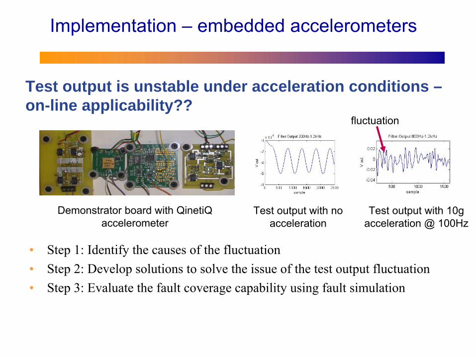
Implementation –
embedded accelerometers
Test output is unstable under acceleration conditions – on-line applicability??
•
Step 1: Identify the causes of the fluctuation•
Step 2: Develop solutions to solve the issue of the test output fluctuation
•
Step 3: Evaluate the fault coverage capability using fault simulation
Demonstrator board with QinetiQ accelerometer
Test output with no acceleration
Test output with 10g acceleration @ 100Hz
fluctuation

Solution –
encoding of test stimuli
•
Encoding the test stimulus
Sensor
Acceleration
Carrier
HP
VoutLP1
+×LFSRLFSR
×
LP2LP2
LP3Cov.
Cor.
Cov.
Cor.Demod.
Vdem
Vcode
Cov
El/AccEl/Acc
Cor
Generation of a pseudo-random bit
code sequence
Modulation of the test sine wave by the code
Test outputs
Operational output
Novel architecture
•
A pseudo-random code sequence modulates the test sine wave•
The code is retrieved by demodulation at the output
•
Covariance and correlation algorithms are applied•
The covariance gives a value related to the sensor sensitivity
•
The correlation gives information on the integrity of the covariance

Application to RF MEMS switch
Bridge Dielectric
Substrate
UP DOWN
Conductor
Cup
/ Cdown
RF in RF out
RF choke
DC blockDC block
Vbias
Switch model with the biasing circuitry in a shunt configuration
Raytheon/TI* switch:Cup = 35fF
(Insertion loss@10GHz = 0.025 dB)Cdown
= 3.5pF
(Isolation@10GHz = 15 dB)
*Raytheon/TI switch
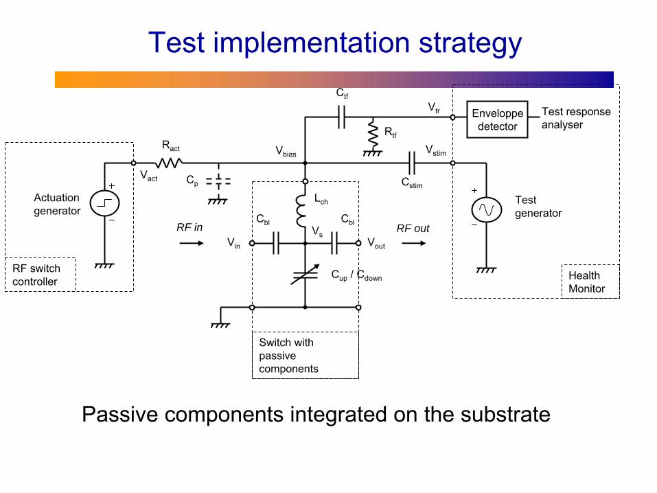
Test implementation strategy
Cup
/ Cdown
RF in RF out
Vbias
Actuation generator
Test generator
Cp
RF switch controller
Test response analyser
Health Monitor
Ract
Rtf
Ctf
Enveloppe
detector
Cstim
Cbl Cbl
Lch
Switch with passive components
Vin Vout
Vs
Vstim
Vtr
Vact
Passive components integrated on the substrate
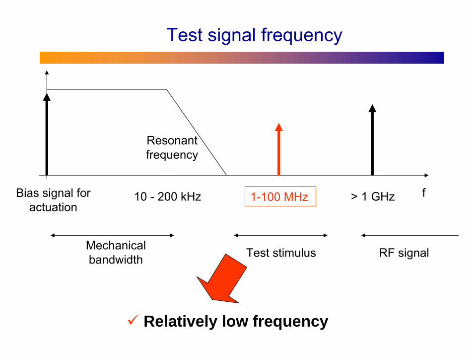
Test signal frequency
10 -
200 kHz fBias signal for actuation
Resonant frequency
Mechanical bandwidth
1-100 MHz > 1 GHz
Test stimulus RF signal
Relatively low frequency
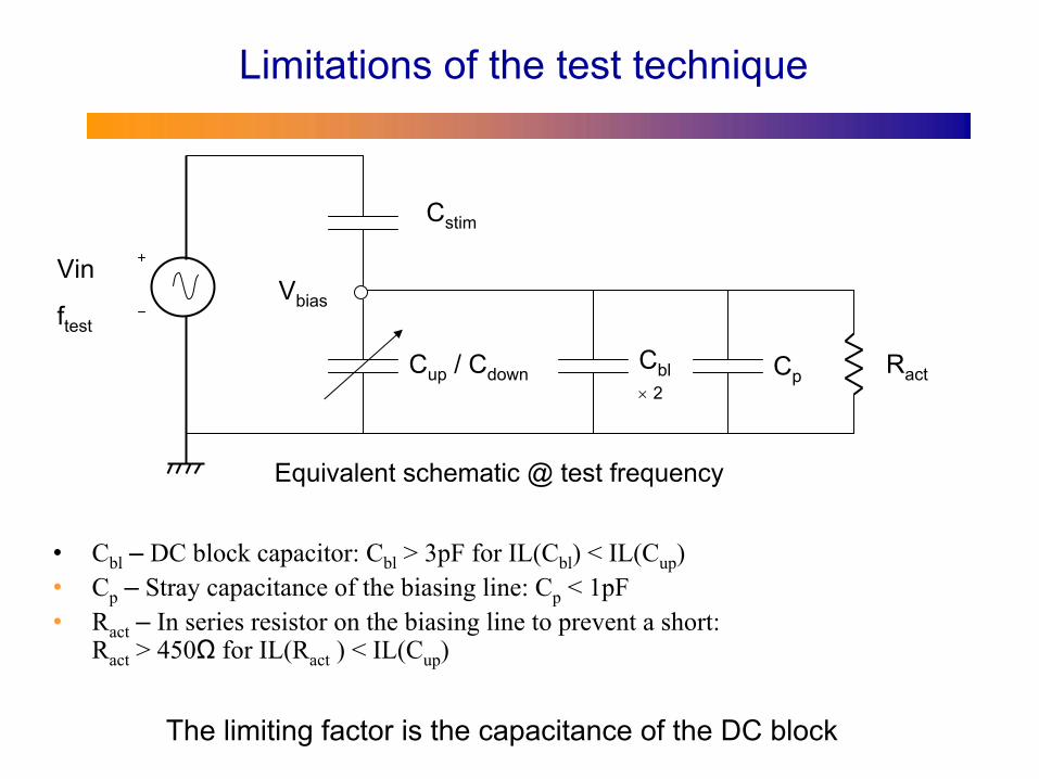
Limitations of the test technique
Cstim
Vin
ftest
Cup
/ Cdown
Vbias
Cbl×
2
Equivalent schematic @ test frequency
Cp Ract
•
Cbl
–
DC block capacitor: Cbl
> 3pF for IL(Cbl
) < IL(Cup
)•
Cp
–
Stray capacitance of the biasing line: Cp
< 1pF•
Ract
–
In series resistor on the biasing line to prevent a short: Ract
> 450Ω
for IL(Ract
) < IL(Cup
)
The limiting factor is the capacitance of the DC block
Conclusions
•
Work to date focused around silicon based WL- SiP
–
Embedded health monitoring–
Strategies for non-electrical functions
–
Reliability simulation –
structure & assembly•
Impact of underfill
on solder reliability
•
Impact of moulding process•
Impact of fan-out
•
Analytical reliability prediction strategies developed–
Extend to SoP
–
eg. Ceramic based
–
Investigate integration into EDA tools