synthesis and characterisation of graphene hybrid...
TRANSCRIPT
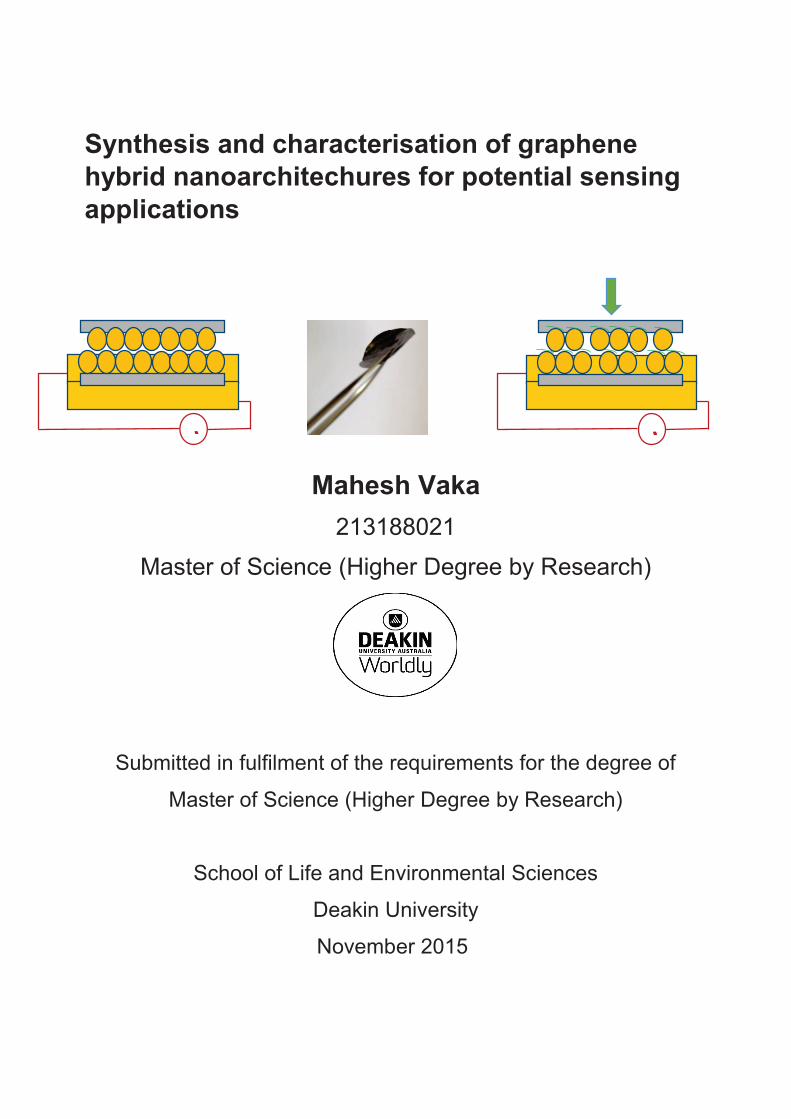
Synthesis and characterisation of graphene hybrid nanoarchitechures for potential sensing applications
Mahesh Vaka 213188021
Master of Science (Higher Degree by Research)
Submitted in fulfilment of the requirements for the degree of
Master of Science (Higher Degree by Research)
School of Life and Environmental Sciences
Deakin University
November 2015
V V


iii
Acknowledgement
First of all, I would like to say thanks to Deakin University for giving me the opportunity to
undertake my Master of Science project at the School of Life & Environmental Science.
Foremost, I would like to show my honour and express my gratitude to my supervisor Dr.
Wenrong Yang for his patience, guidance, helping, sharing his scientific knowledge and
constant encouragement throughout the project.
It’s honour to acknowledge Dr. Colin Barrow, my Co-supervisor who funded me for all the
chemicals and equipment’s which I required during the course of my project.
It’s my pleasure to thank Dr. Xavier Conlan, myCo-supervisor who helped with his valuable
suggestions and encouragement.
Special thanks to Motilal and Tej for helping with my thesis and for their valuable time and
great suggestions and supportive throughout my Master of Science.
Hearty thanks to Dr. Munish Puri and his lab members who helped with the equipment.
Sincere thanks to Dr. Nguyen Dam Nam who helped me with EIS data and valuable
suggestions with experimental data.
I would like to thank all my friends, especially my close friends (Ranjith, Shashank, Aditya
Potti, Thanuja, Mrudhula and Lavanya) and lab members who helped me in times and support
me and boosts my spirit throughout my project.
Last but not least, I dedicate this work and my career to my Dad, Mom, Grandfather and
brothers who have been with me all the time and supporting me both financially and
emotionally.
iv
Conference poster presentation
Mahesh Vaka, Motilal Mathesh, Da Li, Alireza Dijabi, Colin Barrow, Conlan, X and Wenrong
Yang
The application of Graphene based materials for electrochemical actuators presented at 19th
Australia and New Zealand Electrochemistry Symposiumheld at Melbourne on 2013.
Mahesh, V, Motilal, M, Li, D,Barrow, C J, Conlan, X and Yang, W*
A highly sensitive strain gauge using a hybrid graphene material presented at RACI national
congress held at Adelaide on December 2014.
Manuscripts under preparation
Mahesh et.al; Efficient electron transfer pathways: New class of graphene based electrodes.
v
List of Abbreviations
AuNPs Gold nanoparticles
Gr Graphene
GO Graphene Oxide
CRGO’s Chemically reduced graphene oxide
Cys Cystamine sulphate hydrate
ET Electron Transfer
SAM Self-assembled Monolayer
But Butanethiol
Hex Hexanethiol
Oct Octanethiol
Undec Undecanethiol
MBA Mercaptobutanoic acid
MHA Mercaptohexanoic acid
MOA Mercaptooctanoic acid
MUA Mercaptoundecanoic acid
DMF N,N-Dimethylformamide
KCl Potassium Chloride
K3[Fe(CN)6] Potassium ferricyanide H2O2 Hydrogen Peroxide
H2SO4 Sulphuric acid
HCl Hydrochloric acid
KMnO4 Potassium permagnate
mM Millimolar
Rct Charge transfer
Kapp Rate of charge transfer
vi
mN-1 Millinewton
μm Micrometer
MP 11 Microperoxidase
Nm Nanometer
AuNWs Gold nanowires
SWCNTs Single walled carbon nanotubes
MWCNTs Multiwalled carbon nanotubes
CNTs Carbon nanotubes
mg milligram
ml millilitre
Pa Pascals
kPa Kilopascals
mins Minutes
ms milliseconds CV Cyclic Voltammetry
CA Chronoamperometry
EIS Electrochemical Impedance Spectroscopy
dH2O Distilled water
UV-VIS Ultra Violet Visible Spectroscopy
FT-IR Fourier Transform Infrared Spectroscopy
SEM Scanning Electron Microscopy
TEM Transmission Electron Microscopy

vii
Table of Contents
Access to Thesis ……………………………………………………………………………….. i
Student declaration …………………………………………………………………………….. ii
Acknowledgement ..............................................................................................................iii
Conference poster presentation .......................................................................................iv
List of Abbreviations .......................................................................................................... v
List of Figures ..................................................................................................................... x
List of Tables ......................................................................................................................xi
Abstract ............................................................................................................................... 1
Chapter 1- Review of literature .......................................................................................... 2
1.1 Introduction ................................................................................................................... 2
1.2 Hybrid materials ........................................................................................................... 3
1.3 Nanocomposites ........................................................................................................... 3
1.4 Development of Hybrid Materials ................................................................................ 4
1.4.1 Graphene .................................................................................................................... 5
1.4.2 Graphene History....................................................................................................... 6
1.4.3 Graphene with Metals ................................................................................................ 8
1.4.4 Graphene with Thiols ................................................................................................ 8
1.5 Graphene Nanoelectrodes ..........................................................................................11
1.6 Graphene based material for actuators .....................................................................13
1.7 Graphene in touch screen technology ......................................................................15
1.8 Other applications of Graphene .................................................................................16
1.9 APPLICATIONS OF GRAPHENE AND ITS DERIVATIVES .........................................17
1.9.1 Electronic nanodevices ............................................................................................17
viii
1.9.1.1 Field effect transistor (FET) ........................................................................................................... 17
1.9.1.2 Energy Storage Devices ................................................................................................................. 19
1.9.1.3 Lithium Ion Battery ........................................................................................................................ 19
1.9.1.4 Ultra capacitor ............................................................................................................................... 20
1.9.2 Sensors .....................................................................................................................21
1.9.2.1 Electronic sensors .......................................................................................................................... 21
1.9.2.2 Electrochemical sensors ................................................................................................................ 22
1.9.2.3 Biosensors ...................................................................................................................................... 23
1.9.3 Bio-medical applications .........................................................................................24
1.9.3.1 Gene delivery ................................................................................................................................. 24
1.9.3.2 Drug Delivery ................................................................................................................................. 25
1.9.3.3 Tissue Engineering ......................................................................................................................... 26
1.9.3.4 Cancer Therapy .............................................................................................................................. 26
CHAPTER 2 – Materials & Methods .................................................................................28
2.1 Synthesis of AuNPs .....................................................................................................28
2.1.2 Surface Functionalisation of AuNPs .......................................................................28
2.1.3 Hybrid Film Preparation ...........................................................................................28
2.1.4 Preparation of CRGOs ..............................................................................................29
2.1.5 Stepwise preparation of various CRGOs modified gold electrode ......................29
2.2 Instrumentation, Acquisition Parameters and Sample Preparation ........................30
2.2.1 UV-Visible Spectroscopy (UV-Vis) ..........................................................................30
2.2.2 Attenuated Total reflection Fourier Transform Infra Red (ATR-FTIR) ..................30
2.2.3 Raman Spectroscopy ...............................................................................................30
2.2.4 Scanning Electron Microscopy (SEM) ....................................................................31
2.2.5 Transmission Electron Microscopy (TEM) .............................................................31
2.2.6 Potentiostat ...............................................................................................................31
2.2.7 Electrochemical measurements ..............................................................................31
Chapter 3 - Graphene based hybrid actuator for the potential application of artificial
muscle ................................................................................................................................33
ix
3.1 Introduction ..................................................................................................................33
3.2 Result and Discussion ................................................................................................35
3.3 Conclusion ...................................................................................................................41
CHAPTER 4 - Highly sensitive pressure sensor based on graphene hybrids .............43
4.1 Introduction ..................................................................................................................43
4.2 Results and Discussion ..............................................................................................45
4.3 Conclusion ...................................................................................................................52
Chapter 5 - Efficient electron transfer pathways: New class of graphene based
electrodes ...........................................................................................................................53
5.1. Introduction .................................................................................................................53
5.2 Results and Discussion ..............................................................................................55
5.2.1 Electrochemical studies ...........................................................................................55
5.3 Conclusion: ..................................................................................................................65
Chapter 6 – Summary and future perspective ................................................................66
6.1 A graphene hybrid Actuator .......................................................................................66
6.2 A highly sensitive pressure sensor based on graphene hybrid ..............................67
6.3 A new class of graphene electrode ............................................................................68
6.4 Future Perspective ......................................................................................................68
7 References ......................................................................................................................70
8 Appendices .....................................................................................................................77
x
List of Figures
Figure 1Armchair (blue) and zigzag (red) edges in monolayer graphene8. ............................................. 3 Figure 2 Nanocomposites Design Space11 ................................................................................................... 4 Figure 3 Different graphene forms17. ............................................................................................................. 6 Figure 4 Sp2-hybridization of carbon atoms monolayer model in graphene. The appropriate crystalline structure of graphene is a hexagonal grid19. .............................................................................. 7 Figure 5 Graphical representation of the protocol for the fabrication of a Graphene/SAM altered gold electrode and the heterogeneous ET mechanism on the Graphene altered electrode32. ................... 10 Figure 6 Diagrammatic illustration of four electro modified with SAMs of AET, AHT, AOT, and AUT and then subsequently altered with a monolayer of gold nanoparticles33.............................................. 11 Figure 7 Voltammetric responses of an Au/SAM modified graphene electrode in the solution of 1 M KCl containing 10 mM Ru(NH3)6 3+. Potential scanning rate: 10 mV/s40. ............................................. 12 Figure 8 Actuation of the bilayer paper sample as a function of relative humidity (%), a) 12, b) 25, c) 49, d) 61, e) 70, and f) 90. White-arrowed side: surface of graphene oxide layer44. ........................... 14 Figure 9 Illustrates the Change in resistance with the strain for a NP film which is functionalized by4-NTP52. ............................................................................................................................................................... 16 Figure 10 Graphene Field Effect Transistor70 ............................................................................................. 19 Figure 11 Alternating layers of graphene and tin are used to create a nanoscale composite for renewable lithium ion batteries79 .................................................................................................................. 20 Figure 12 Graphene based ultracapacitor71 ............................................................................................... 21 Figure 13 Represents protein detection by graphene-gold nanoparticle conjugates.86 ....................... 22 Figure 14 Graphene materials used in different sensors to detect biomolecules98 .............................. 24 Figure 15 Graphene material used in cancer therapy112 .......................................................................... 27 Figure 16 Represents the self-assembly of hybrid graphene film (Mahesh, Visual Molecular Dynamics). ....................................................................................................................................................... 35 Figure 17 Pictorial representation of graphene hybrid fabrication (Mahesh, PowerPoint). ................. 35 Figure 18 Surface properties: a) UV-Vis for Gr, AuNPs, AuNPs coated cystamine and Gr-AuNPs coated cystamine. b) Zeta potential Gr and Gr-functionalised gold NPs in aqueous dispersion. ...... 37 Figure 19 SEM image: Cross-section of graphene hybrid film. ............................................................... 38 Figure 20 Schematic representation graphene hybrid actuator a,b,c) Response of gr-hybrid actuator before and after applying different potential range ± 0.6, d) Front view of gr hybrid actuator (Mahesh, Power Point). ................................................................................................................................. 38 Figure 21 Deflection ∂ (swelling of the film) of the graphene hybrid actuator as a function of time, wave potential at ± 0.6 V. a) functionalised gold NPs sandwiched between graphene layers. b) thiourea functionalised gold NPs sandwiched between graphene layers. ............................................. 39 Figure 22 Actuator response on applying ± 0.6 V. a,b) Current as a function of time arising from charging and discharging current. c,d) Anson plot represents charging and discharging current. .... 40 Figure 23 Cyclic voltammograms of the graphene hybrid film before stability test and after 2000 cycles ................................................................................................................................................................ 41 Figure 24 Pictorial representation of the hybrid film (Mahesh, PowerPoint) ......................................... 45 Figure 25 SEM images a.) Cross-section of Gr hybrid film b.) Shows side view for Gr hybrid film. .. 46 Figure 26 TEM images a.) AuNPs coated Cyst b.) Shows the functionalised gold NPs on the Gr sheet. ................................................................................................................................................................ 47 Figure 27 Raman spectra of functionalized gold nanoparticles before and after binding on graphene sheets and cystamine. ................................................................................................................................... 48 Figure 28 a.) FTIR spectra of Gr, Gr hybrid and cystamine sulfate hydrate.......................................... 49

xi
Figure 29 a.) Relative change in resistance with respective to applied force. The sensitivity factor at the highest point shows 0.005 mN-1. b.) Detection of current response while loading and unloading of pressure by pressing. c) Plot shows current response for Tap and release. d) Plot for current response as a function of time for applied pressure. ................................................................................ 51 Figure 30 Schematic representation of CRGO’s self-assembly process on to the gold electrode (Mahesh, Power Point). ................................................................................................................................. 54 Figure 31 a) CVs of different COOH terminated thiols modified SAM electrode b) CVs of different CH3 terminated thiols modified SAM electrode in 1 M KCl of 10 mM Fe (CN)6
3-. ................................. 55 Figure 32A Cyclic voltammograms of a.) MBA with CRGO’s with different reduction times, b.) MHA with CRGO’s with different reduction times, and c.) MOA with CRGO’s with different reduction times and d.) MUA with CRGO’s with different reduction times in 10 mM Fe(CN)6
3- in1 M KCl solution. The scan rate is 100 mV/s..................................................................................................................................... 57
List of Tables Table 1 Electrochemical data obtained for different SAMs on gold electrode before and after modification with CRGO’s with different reduction times from impedance plots in 10 mM Fe(CN)6
3-
in1 M KCl solution. .......................................................................................................................................... 62 Table 2 Electrochemical parameters for SAM-modified Au electrode before and after adsorption of CRGO’s with different reduction times. ....................................................................................................... 64
1 | P a g e
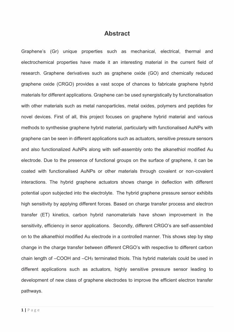
Abstract
Graphene’s (Gr) unique properties such as mechanical, electrical, thermal and
electrochemical properties have made it an interesting material in the current field of
research. Graphene derivatives such as graphene oxide (GO) and chemically reduced
graphene oxide (CRGO) provides a vast scope of chances to fabricate graphene hybrid
materials for different applications. Graphene can be used synergistically by functionalisation
with other materials such as metal nanoparticles, metal oxides, polymers and peptides for
novel devices. First of all, this project focuses on graphene hybrid material and various
methods to synthesise graphene hybrid material, particularly with functionalised AuNPs with
graphene can be seen in different applications such as actuators, sensitive pressure sensors
and also functionalized AuNPs along with self-assembly onto the alkanethiol modified Au
electrode. Due to the presence of functional groups on the surface of graphene, it can be
coated with functionalised AuNPs or other materials through covalent or non-covalent
interactions. The hybrid graphene actuators shows change in deflection with different
potential upon subjected into the electrolyte. The hybrid graphene pressure sensor exhibits
high sensitivity by applying different forces. Based on charge transfer process and electron
transfer (ET) kinetics, carbon hybrid nanomaterials have shown improvement in the
sensitivity, efficiency in senor applications. Secondly, different CRGO’s are self-assembled
on to the alkanethiol modified Au electrode in a controlled manner. This shows step by step
change in the charge transfer between different CRGO’s with respective to different carbon
chain length of –COOH and –CH3 terminated thiols. This hybrid materials could be used in
different applications such as actuators, highly sensitive pressure sensor leading to
development of new class of graphene electrodes to improve the efficient electron transfer
pathways.
2 | P a g e
Chapter 1- Review of literature
1.1 Introduction
Nanotechnology can be defined as the technology which is developed with particles of
dimensions 10-9 m and application of physical, chemical and biological molecules at the
scale which goes from single atoms or molecules to the submicron dimensions, as well as
combination of the resulting nanostructures into high architecture frameworks1.
Carbon has been known and studied from ancient times. It has two allotropes namely,
graphite and diamonds. Utilization of graphite dates back to 6000 years, but the utilization of
graphene, single layer of graphiteis just 50 years old and was studiedfor its high conductivity2.
From that point forward graphite as single atom was a captivating field for examination. In
2010, Andre Geim and Konstantin Novoselov won the Nobel Prize for discovery of single
layer of carbon which was stable, as conductive as copper, and as small as not even helium
molecule could go pass through it3. Since, then graphene and carbon nanotubes has been
broadly studied because of its electrical, mechanical, thermal and structural properties. This
nano size graphene is cutting edge material to be utilized as biosensor. The graphene film
thickness could be controlled from tens of nanometers to 10 μm4. Graphene sheets are
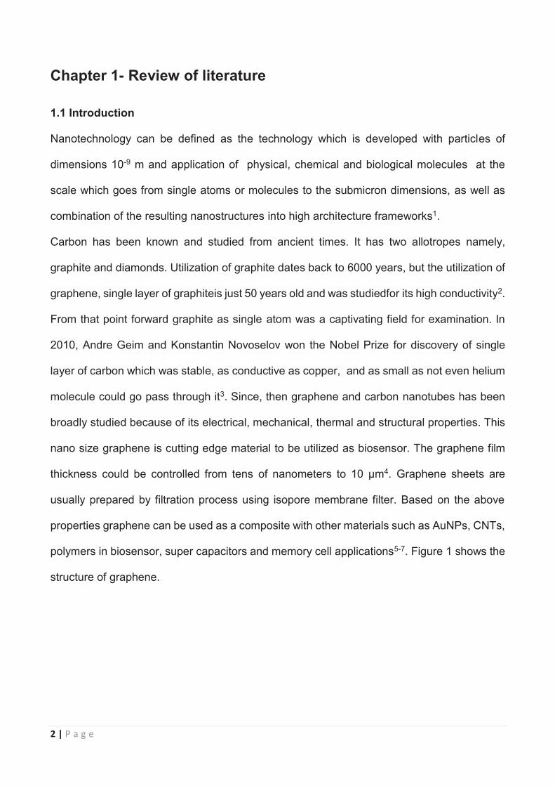
usually prepared by filtration process using isopore membrane filter. Based on the above
properties graphene can be used as a composite with other materials such as AuNPs, CNTs,
polymers in biosensor, super capacitors and memory cell applications5-7. Figure 1 shows the
structure of graphene.

3 | P a g e
Figure 1Armchair (blue) and zigzag (red) edges in monolayer graphene8.
1.2 Hybrid materials
The hybrid nanomaterials are designed through assembly of different molecules on the
carbon nanomaterial. The carbon nanomaterial has been covered by metals, biomolecules
and polymers as a second material which shows huge potential in future applications such
as senors, energy storage and supercapacitors9, 10. A hybrid material is generally defined as
a material which comprises of two moieties that are mixed on the molecular scale. Usually
one of the material is active and the other one is inactive in nature. Category I hybrids
represents the weak interaction between the two compounds like van der Waals, electrostatic
interactions or hydrogen bonding. Category II hybrids illustrate strong covalent interactions
between the two components11.
1.3 Nanocomposites
Nanocomposites is the combination of carbon nanomaterial with other materials in which one
acts as a filler (nanowires, nanotubes, nanoparticles) and other acts as a support or matrix
(ceramics, polymers).The main concept of the nanocomposite development is to integrate
specific properties of one material into another to achieve high performance and also to
enhance the electrical/ mechanical properties9, 12. Usually nanocomposites are prepared by
random mixing of two different materials and hence exhibiting non-uniform properties. This
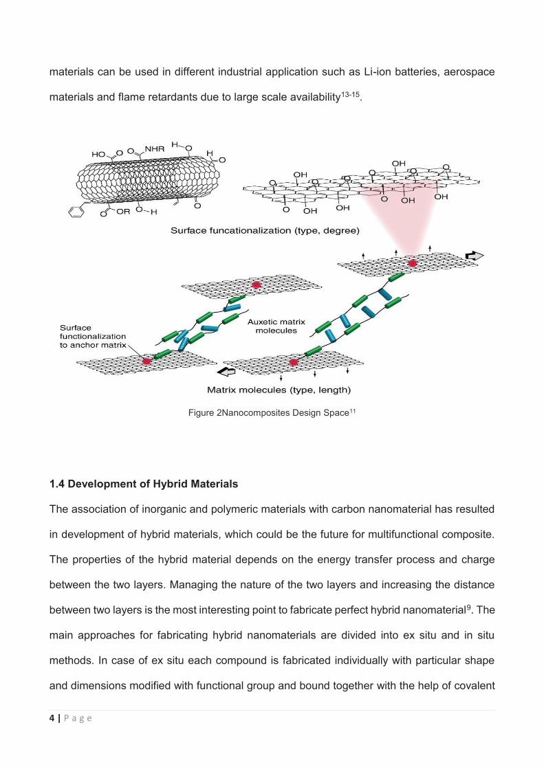
4 | P a g e
materials can be used in different industrial application such as Li-ion batteries, aerospace
materials and flame retardants due to large scale availability13-15.
Figure 2Nanocomposites Design Space11
1.4 Development of Hybrid Materials
The association of inorganic and polymeric materials with carbon nanomaterial has resulted
in development of hybrid materials, which could be the future for multifunctional composite.
The properties of the hybrid material depends on the energy transfer process and charge
between the two layers. Managing the nature of the two layers and increasing the distance
between two layers is the most interesting point to fabricate perfect hybrid nanomaterial9. The
main approaches for fabricating hybrid nanomaterials are divided into ex situ and in situ
methods. In case of ex situ each compound is fabricated individually with particular shape
and dimensions modified with functional group and bound together with the help of covalent
5 | P a g e
or non-covalent interactions. In the other case, one compound is directly synthesized on the
surface of other compound directly16.
1.4.1 Graphene
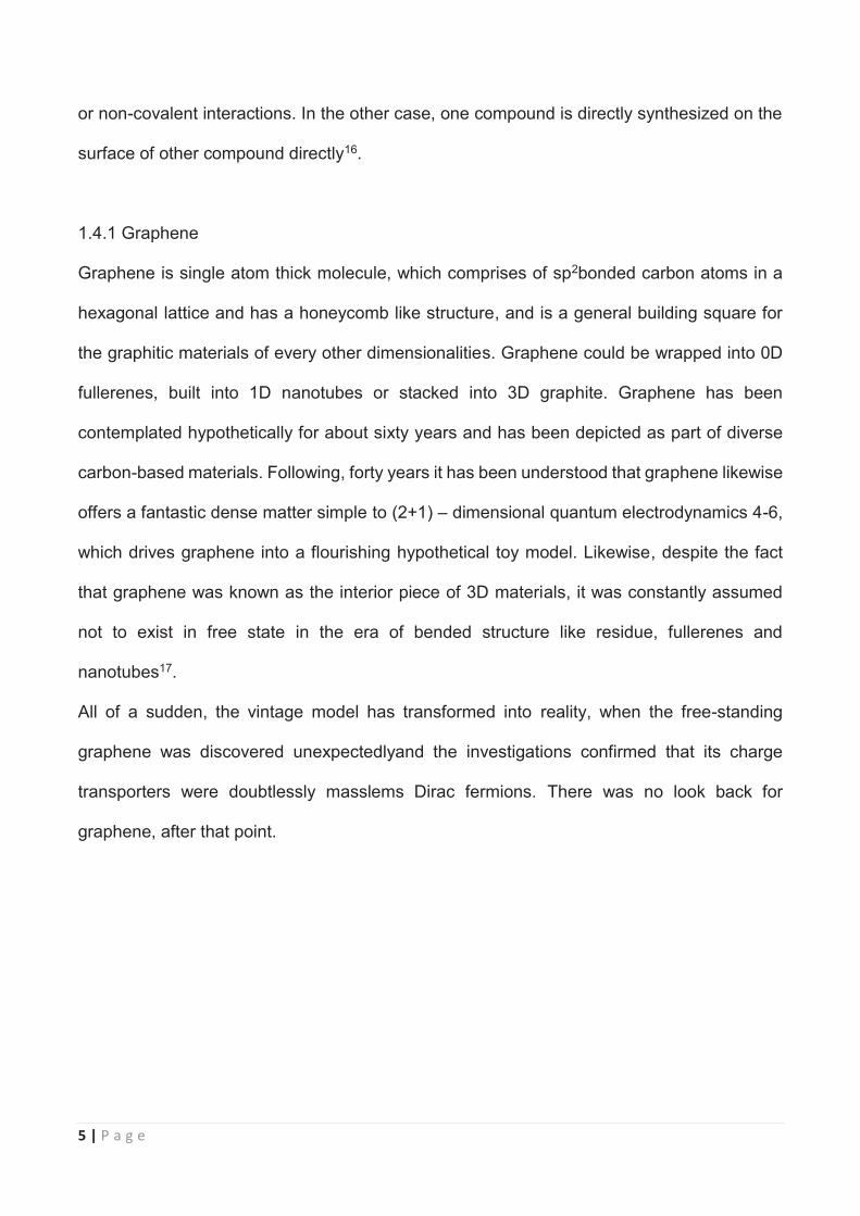
Graphene is single atom thick molecule, which comprises of sp2bonded carbon atoms in a
hexagonal lattice and has a honeycomb like structure, and is a general building square for
the graphitic materials of every other dimensionalities. Graphene could be wrapped into 0D
fullerenes, built into 1D nanotubes or stacked into 3D graphite. Graphene has been
contemplated hypothetically for about sixty years and has been depicted as part of diverse
carbon-based materials. Following, forty years it has been understood that graphene likewise
offers a fantastic dense matter simple to (2+1) – dimensional quantum electrodynamics 4-6,
which drives graphene into a flourishing hypothetical toy model. Likewise, despite the fact
that graphene was known as the interior piece of 3D materials, it was constantly assumed
not to exist in free state in the era of bended structure like residue, fullerenes and
nanotubes17.
All of a sudden, the vintage model has transformed into reality, when the free-standing
graphene was discovered unexpectedlyand the investigations confirmed that its charge
transporters were doubtlessly masslems Dirac fermions. There was no look back for
graphene, after that point.
6 | P a g e
Figure 3Different graphene forms17.
1.4.2 Graphene History
Once graphene was discovered, it had to be characterised to learn about the nature and
properties of 2D crystals. It has been showcased that the electronic structures create with the
layer numbers, drawing nearer as far as possible for graphite as of now at 10 layers.
Additionally, just graphene and, to the great estimate, its bilayer has straightforward
electronic spectra: they are both the zero-gap semiconductors with one sort of electrons and
one kind of gaps. For three and more layers, the spectra will get progressively troublesome.
Different charge transporters show up and the valence groups begin to eminently cover. This
will permit one to separate between single-, twofold, and couple of (3to <10) layer graphene
as three various types of 2D crystals. Structures which are thicker must be considered, to
every one of the purposes and reasons, as thin films of graphite18. From the experimental
view point, such type of definition is also sensible. The screening length in graphite is only
≈5Å and so one should distinguish between the surface and the bulk even for films as thin as
5 layers19.
7 | P a g e
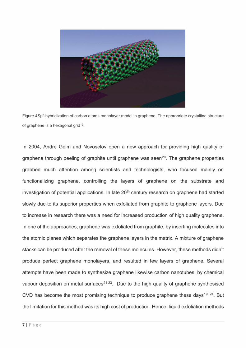
Figure 4Sp2-hybridization of carbon atoms monolayer model in graphene. The appropriate crystalline structure
of graphene is a hexagonal grid19.
In 2004, Andre Geim and Novoselov open a new approach for providing high quality of
graphene through peeling of graphite until graphene was seen20. The graphene properties
grabbed much attention among scientists and technologists, who focused mainly on
functionalizing graphene, controlling the layers of graphene on the substrate and
investigation of potential applications. In late 20th century research on graphene had started
slowly due to its superior properties when exfoliated from graphite to graphene layers. Due
to increase in research there was a need for increased production of high quality graphene.
In one of the approaches, graphene was exfoliated from graphite, by inserting molecules into
the atomic planes which separates the graphene layers in the matrix. A mixture of graphene
stacks can be produced after the removal of these molecules. However, these methods didn’t
produce perfect graphene monolayers, and resulted in few layers of graphene. Several
attempts have been made to synthesize graphene likewise carbon nanotubes, by chemical
vapour deposition on metal surfaces21-23. Due to the high quality of graphene synthesised
CVD has become the most promising technique to produce graphene these days19, 24. But
the limitation for this method was its high cost of production. Hence, liquid exfoliation methods
8 | P a g e
were established by reducing graphene oxide into graphene25, which resulted in decrease in
cost of production, together with increase in product.
1.4.3 Graphene with Metals
In general, fabrication of metal-matrix composites reinforced by graphene inclusions (sheets,
nanoplatelets) is very challenging. There has been few successful studies in this area which
are listed below, below are some of the examples focused on fabrication of metal graphene
nanocomposites with enhanced mechanical properties:
Wang and co-workers fabricated Al-graphene nanocomposites showing a dramatic
enhancement in strength, as compared to their graphene-free counterpart. This was achieved
by a novel approach based on flake powder metallurgy.
Wang with co-workers performed tensile tests with specimens of 5mmdiameter and
25mmgauge length machined from extruded rods consisting of Al-matrix reinforced by 0.3
wt. % graphene nanosheets. A good correlation was observed between the theoretical and
experimental values for mechanical strength of the Al-graphene nanocomposites. Based on
their results, Wang with co-coworkers concluded that reinforcement by graphene nanosheets
is most effective for Al-matrix materials and have a huge potential for applications26. There
still remains huge room of space for improvement of strength and other mechanical
characteristics exhibited by Al-matrix nanocomposites due to their strengthening by graphene
nanosheets.
1.4.4 Graphene with Thiols
In recent years, because of the advancement and development of commercial ventures, the
levels of contamination of water with heavy metals has increased. Contamination of water
bodies is a big issue for biological network and furthermore for the human life. Among these
9 | P a g e
different heavy metal contaminations, mercury stands out to be most hazardous because of
its poisonous nature. Various types of adsorbents have been utilized to remove Hg2+ from
the modern wastewaters. But still, there is a need to have improved absorbents. Addressing
this issue, a thiol-functionalized magnetite/graphene oxide (MGO) was synthesized for
effective adsorption of Hg2+by a two stage response27. It showcased a more prominent
adsorption ability as compared to graphene oxide and MGO separately, because of the
consolidated adsorption of thiol groups and magnetite nanocrystals. The absorption capacity
increased to 289.9 mg g−1with solution of 100 mg l-1 Hg2+ concentration. The adsorption of
Hg2+ by thiol-functionalized MGO fits well with the Freundlich isotherm and follows pseudo-
second-order reaction. Thiol-funcionalized adsorbents demonstrated a specific binding of
Hg2+ because of the complexation of Hg2+with thiol groups when they are in close vicinity.
Iron oxide nanocrystalsenhanced the absorption capacities because of their high specific
surface area28, 29. Another advantage of using iron oxide was the ease of removal of
adsorbate from wastewater by application of magnetic force. The presence of oxygen
functional groups on graphene oxide allows binding of such metal oxides and grafting of
organic groups to its surface30, 31. In this study, the reserachers havebound Fe3O4
nanoparticles on graphene oxide and grafted thiol groups on the Fe3O4/graphene oxide
(MGO). The thiol-functionalized MGO represented moderately higher Hg2+ adsorption
capacity. The adsorbent can be separated from the water with straightforward process and
reused after it was exchanged over with H+27.
Shao et.al, has examined the electrochemical behavior of the graphene sheets which was
bound to the SAM’s on a gold electrode. The electrochemical behavior of
graphene/SAM/modified electrode was investigated. The gold electrode was modified with
C18SAM followed by controllable adsorption of graphene onto the SAM modified Au electrode.
The graphene/SAM/Au electrode was successfully characterised by using atomic force
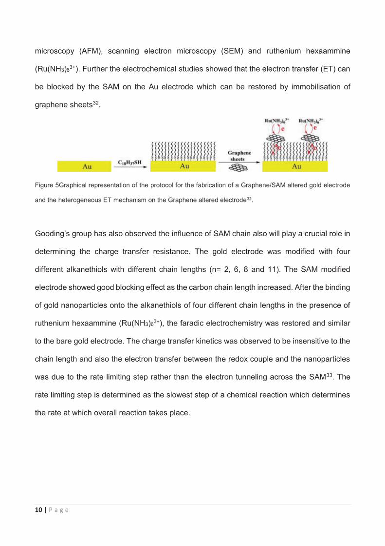
10 | P a g e
microscopy (AFM), scanning electron microscopy (SEM) and ruthenium hexaammine
(Ru(NH3)63+). Further the electrochemical studies showed that the electron transfer (ET) can
be blocked by the SAM on the Au electrode which can be restored by immobilisation of
graphene sheets32.
Figure 5Graphical representation of the protocol for the fabrication of a Graphene/SAM altered gold electrode
and the heterogeneous ET mechanism on the Graphene altered electrode32.
Gooding’s group has also observed the influence of SAM chain also will play a crucial role in
determining the charge transfer resistance. The gold electrode was modified with four
different alkanethiols with different chain lengths (n= 2, 6, 8 and 11). The SAM modified
electrode showed good blocking effect as the carbon chain length increased. After the binding
of gold nanoparticles onto the alkanethiols of four different chain lengths in the presence of
ruthenium hexaammine (Ru(NH3)63+), the faradic electrochemistry was restored and similar
to the bare gold electrode. The charge transfer kinetics was observed to be insensitive to the
chain length and also the electron transfer between the redox couple and the nanoparticles
was due to the rate limiting step rather than the electron tunneling across the SAM33. The
rate limiting step is determined as the slowest step of a chemical reaction which determines
the rate at which overall reaction takes place.
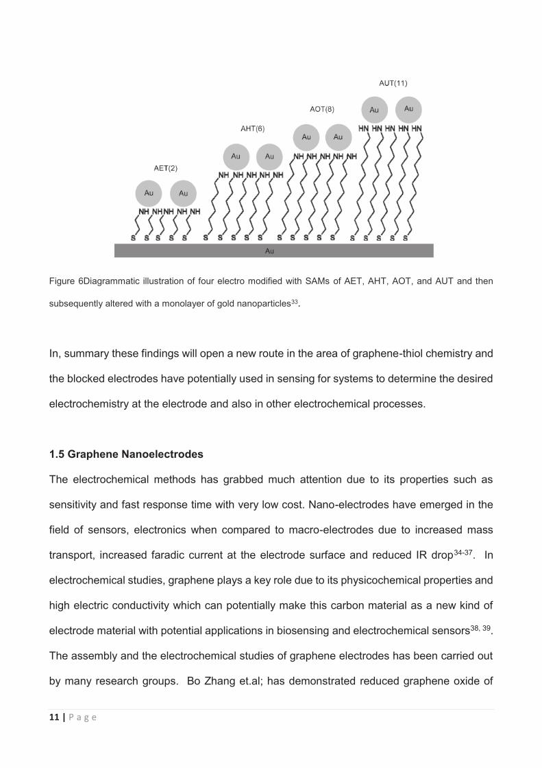
11 | P a g e
Figure 6Diagrammatic illustration of four electro modified with SAMs of AET, AHT, AOT, and AUT and then
subsequently altered with a monolayer of gold nanoparticles33.
In, summary these findings will open a new route in the area of graphene-thiol chemistry and
the blocked electrodes have potentially used in sensing for systems to determine the desired
electrochemistry at the electrode and also in other electrochemical processes.
1.5 Graphene Nanoelectrodes
The electrochemical methods has grabbed much attention due to its properties such as
sensitivity and fast response time with very low cost. Nano-electrodes have emerged in the
field of sensors, electronics when compared to macro-electrodes due to increased mass
transport, increased faradic current at the electrode surface and reduced IR drop34-37. In
electrochemical studies, graphene plays a key role due to its physicochemical properties and
high electric conductivity which can potentially make this carbon material as a new kind of
electrode material with potential applications in biosensing and electrochemical sensors38, 39.
The assembly and the electrochemical studies of graphene electrodes has been carried out
by many research groups. Bo Zhang et.al; has demonstrated reduced graphene oxide of
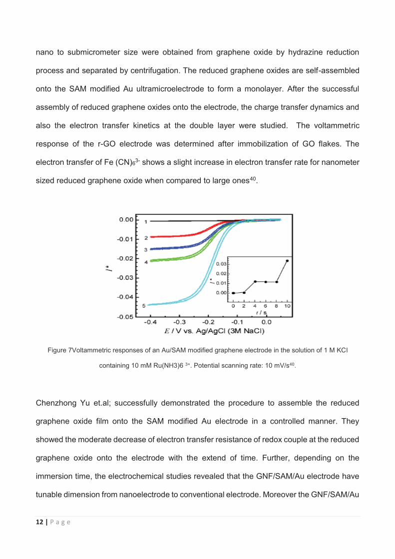
12 | P a g e
nano to submicrometer size were obtained from graphene oxide by hydrazine reduction
process and separated by centrifugation. The reduced graphene oxides are self-assembled
onto the SAM modified Au ultramicroelectrode to form a monolayer. After the successful
assembly of reduced graphene oxides onto the electrode, the charge transfer dynamics and
also the electron transfer kinetics at the double layer were studied. The voltammetric
response of the r-GO electrode was determined after immobilization of GO flakes. The
electron transfer of Fe (CN)63- shows a slight increase in electron transfer rate for nanometer
sized reduced graphene oxide when compared to large ones40.
Figure 7Voltammetric responses of an Au/SAM modified graphene electrode in the solution of 1 M KCl
containing 10 mM Ru(NH3)6 3+. Potential scanning rate: 10 mV/s40.
Chenzhong Yu et.al; successfully demonstrated the procedure to assemble the reduced
graphene oxide film onto the SAM modified Au electrode in a controlled manner. They
showed the moderate decrease of electron transfer resistance of redox couple at the reduced
graphene oxide onto the electrode with the extend of time. Further, depending on the
immersion time, the electrochemical studies revealed that the GNF/SAM/Au electrode have
tunable dimension from nanoelectrode to conventional electrode. Moreover the GNF/SAM/Au
13 | P a g e
electrode shows good electrocatalytic activity towards uric acid, dopamine and ascorbic
acid41.
In summary, these graphene nanoelectrodes in future can be used in electrochemical
investigations and more practical applications such as electroanalysis in vivo and in vitro.
1.6 Graphene based material for actuators
An actuator is a device which converts one form of energy such as thermal, electrical, light
into mechanical form. Under these external stimuli, actuators can undergo change in shape,
volume and other mechanical properties, in order to convert one form of energy into
mechanical energy42.
The ordinary activation materials such as piezoelectric, ferroelectric and conducting polymer
materials experience problems related to lower adaptability, higher driving voltages and lower
vitality. In contrast, graphene shows astounding mechanical, electrical, and optical angles
and chemical security, which has provoked graphene to be studied as an actuation incitation
material. Different actuation components and the required future improvements has been
reported below. Graphene subordinate materials with composites of different superior quality
components which are similar in material abundance, mechanical quality together with more
prominent actuation execution are anticipated to have more prominent probability for the
application in the cutting edge actuators43.
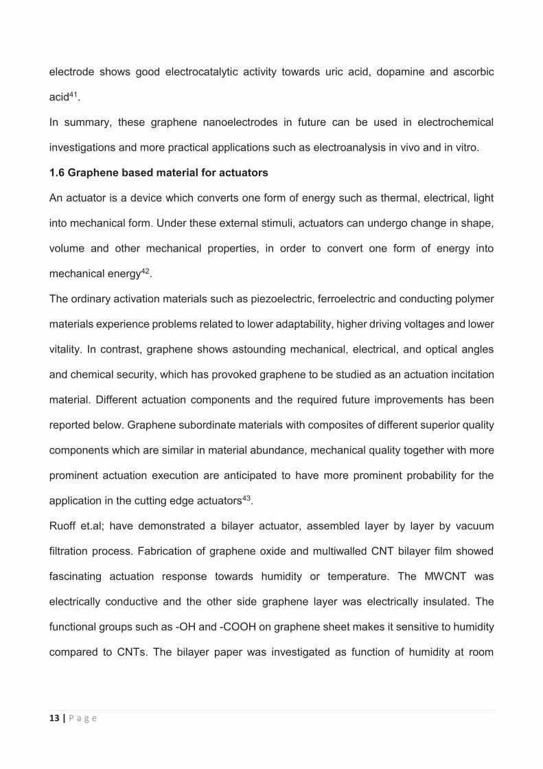
Ruoff et.al; have demonstrated a bilayer actuator, assembled layer by layer by vacuum
filtration process. Fabrication of graphene oxide and multiwalled CNT bilayer film showed
fascinating actuation response towards humidity or temperature. The MWCNT was
electrically conductive and the other side graphene layer was electrically insulated. The
functional groups such as -OH and -COOH on graphene sheet makes it sensitive to humidity
compared to CNTs. The bilayer paper was investigated as function of humidity at room
14 | P a g e
temperature. As, the temperature changed, the bilayer paper curls in two different directions
as shown in the Figure 744.
Figure 8 Actuation of the bilayer paper sample as a function of relative humidity (%), a) 12, b) 25, c) 49, d) 61,
e) 70, and f) 90. White-arrowed side: surface of graphene oxide layer44.
Raguse et.al; have successfully prepared a nanoparticle actuator based on gold
nanoparticles functionalised with short bifunctional cystamine hydrochloride. The surface
charge on the gold nanoparticles can be manipulated which helps to carry out the actuation
mechanism by applying different potentials. Based on the surface charge the actuator
showed forward and backward deflection by applying different voltage ± 0.6 V45.
15 | P a g e
1.7 Graphene in touch screen technology
Presently, the touch screen technology has observed a huge overhaul with the introduction
of the graphene-based innovations. Modern touch sensitive screens may utilize indium tin
oxide, a substance that is transparent but carries the electrical currents. One of the
drawbacks of indium tin oxide is its cost, they are expensive and has been put to application
only by few. So replacing the indium tin oxide with the graphene-based compounds would
facilitate for flexible and cheap paper-thin computers and television screens.
Touch sensors are the most sophisticated and emerging area of nanotechnology and are
gaining a great deal of attention due to their applications in human robotics,46 therapeutics47
and diagnostics.48 Sensation of touch is defined as the applied pressure over the specified
area of physical contact between the device and the object. For designing a flexible sensor,
it is necessary to pay special attention to the way the NPs are inserted on to the flexible
sensor. Change in thickness, morphology49 and density50 of the films affect the sensitivity,
selectivity and the overall functionality of NP-based sensor. Different supporting layers have
different adhesion properties corresponding to NP films which can alter the sensing signal51
as well as the sensor’s life. Several biomimetic sensors and strain gauges were successfully
developed by functionalization of gold nanoparticles with different peptides. The change in
resistance, with respect to the change in pressure, plays a key role in designing a flexible
sensor. The behavior of a device depends mostly on parameters like particle size,
interparticle distance and the conductance of linker molecule. Herrmann et al.52 have
successfully developed a sensitive strain gauge by functionalization of gold nanoparticles
with 4-nitrothiophenol (4-NTP). They observed that the sensitivity of the change in resistance
was relative to the change in pressure. To date, no one has completely explored the usage
of functionalized gold nanoparticles in the area of touch sensors and has great future in the
field of medicine, robotics and for the detection of environmental changes.
16 | P a g e
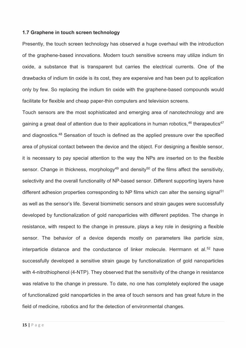
Figure 9 Illustrates the Change in resistance with the strain for a NP film which is functionalized by4-NTP52.
1.8 Other applications of Graphene
Graphene has pulled in much consideration from scientists because of its intriguing
mechanical, electrochemical and electronic properties. Graphene, a solitary nuclear layer of
sp2-fortified carbon atoms firmly stuffed in a two dimensional (2D) honeycomb cross section,
has evoked extraordinary enthusiasm all through established researchers since its revelation.
As a novel nanomaterial, graphene has one of a kind electronic, optical, warm, and
mechanical properties. Graphene and its subordinates have indicated extraordinary
possibilities in numerous fields, for example, nanoelectronics, designing nanocomposite
materials, vitality stockpiling, field impact transistor (FET), natural light emanation diodes
(OLED), sensors, catalysis and biomedical applications (biosensor, biodevices, medication
and quality conveyance, growth treatment and so on.). As of not long ago, a few techniques
have been created for manufacture, development or amalgamation of graphene and its
subordinates. Graphene is mainly exfoliated by mechanical exfoliation of graphite utilizing
glue tapes. Chemical vapour deposition (CVD) has been utilized to develop single and few-
layer graphene sheets on metal surfaces, for example, Ni and Cu. Graphene layers can

17 | P a g e
likewise be synthesized by depositing carbon on carbon-containing substrates like SiC
through high temperature toughening. Chemical oxidation and exfoliated graphite oxide has
been developed utilized to synthesize reduced graphene oxide (rGO) or chemically
functionalized graphene (CFG). Highlighting extraordinary physical and chemical properties
and having dependable engineered routines for both solid and solution-phase processes,
graphene and its subordinates have been functionalised with various functional materials to
shape composites and have been utilized as building blocks for different applications.
1.9 APPLICATIONS OF GRAPHENE AND ITS DERIVATIVES
The headway of newly discovered nanomaterials gives an interesting chance to
advancement in distinctive fields due to their structures, parts and properties. In correlation
with its antecedent, carbon nanotube (CNT), graphene displays a few benefits like minimal
effort, two external surfaces, easy creation and alteration and absence of harmful metal
particles53. Along these lines graphene and its subsidiaries are relied upon to discover
applications in numerous fields, for example, nanoelectronic gadgets, chemical and biological
sensors, energy storage and biomedical fields54.
1.9.1 Electronic nanodevices
Due to the superior electrical conductivity, mechanical flexibility and less expensive,
graphene and the other derivatives of it has got great range of applications in generating light
emitting diode (LED), Field effect transistor (FET), memory and photovoltaic devices55-58.
1.9.1.1 Field effect transistor (FET)
In view of unique band structure, the bearers in graphene are bipolar, with electrons and
openings that can be perseveringly tuned by a gateway electrical field. The electric field affect
in graphene was at first reported by Novoselov et al. in 200420. As indicated by this report,
graphene based FETs exhibited ambipolar qualities with electrons and entire centralization

18 | P a g e
of 1013 sq.cm with mobilities upto 10,000 sq.cm per volt.sec at room temperature. Graphene
FET gadgets with a solitary back entryway have been researched by a few different other
researchers as well59-61.
For the application as transistor, graphene ought to be as quasi one dimensional (1D)
structure with thin width and molecularly smooth edges termed as graphene
nanoribbons(GNRs). These GNRs displays band gap helpful or FET application with
phenomenal exchange rate and high transporter versatility at room temperature.
Consequently the quasi 1D GNRs is a semiconductors with limited vitality band gap62, 63.
Despite the band gap displayed in GNRs, these were exceptionally interesting in with regards
to transporter versatility and creation when compared to graphene.Many research groups
have been working on synthesis of GNR’s using different techniques which includes chemical
and lithographic techniques64-66.
Lu et al. created a high mobility adaptable graphene field-impact transistor with self-healing
door dielectrics for an extensive variety of utilizations in adaptable gadgets67. Szafranek and
his associates have exhibited current immersion and voltage pick up in bilayer graphene field
impact transistor68-70.
In summary, graphene combining with other materials provides a novel route to increase the
performance and mechanical flexibility.
19 | P a g e
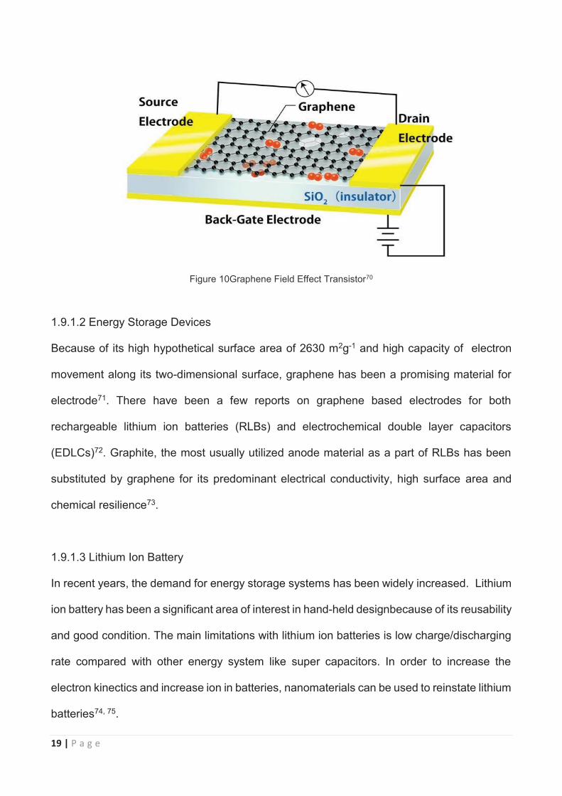
Figure 10Graphene Field Effect Transistor70
1.9.1.2 Energy Storage Devices
Because of its high hypothetical surface area of 2630 m2g-1 and high capacity of electron
movement along its two-dimensional surface, graphene has been a promising material for
electrode71. There have been a few reports on graphene based electrodes for both
rechargeable lithium ion batteries (RLBs) and electrochemical double layer capacitors
(EDLCs)72. Graphite, the most usually utilized anode material as a part of RLBs has been
substituted by graphene for its predominant electrical conductivity, high surface area and
chemical resilience73.
1.9.1.3 Lithium Ion Battery
In recent years, the demand for energy storage systems has been widely increased. Lithium
ion battery has been a significant area of interest in hand-held designbecause of its reusability
and good condition. The main limitations with lithium ion batteries is low charge/discharging
rate compared with other energy system like super capacitors. In order to increase the
electron kinectics and increase ion in batteries, nanomaterials can be used to reinstate lithium
batteries74, 75.
20 | P a g e
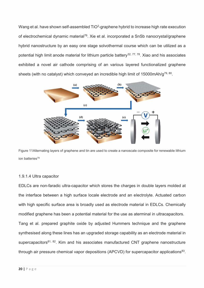
Wang et al. have shown self-assembled TiO2-graphene hybrid to increase high rate execution
of electrochemical dynamic material76. Xie et al. incorporated a SnSb nanocrystal/graphene
hybrid nanostructure by an easy one stage solvothermal course which can be utilized as a
potential high limit anode material for lithium particle battery32, 77, 78. Xiao and his associates
exhibited a novel air cathode comprising of an various layered functionalized graphene
sheets (with no catalyst) which conveyed an incredible high limit of 15000mAh/g79, 80.
Figure 11Alternating layers of graphene and tin are used to create a nanoscale composite for renewable lithium
ion batteries79
1.9.1.4 Ultra capacitor
EDLCs are non-faradic ultra-capacitor which stores the charges in double layers molded at
the interface between a high surface locale electrode and an electrolyte. Actuated carbon
with high specific surface area is broadly used as electrode material in EDLCs. Chemically
modified graphene has been a potential material for the use as aterminal in ultracapacitors.
Tang et al. prepared graphite oxide by adjusted Hummers technique and the graphene
synthesised along these lines has an upgraded storage capability as an electrode material in
supercapacitors81, 82. Kim and his associates manufactured CNT graphene nanostructure
through air pressure chemical vapor depositions (APCVD) for supercapacitor applications83.
21 | P a g e
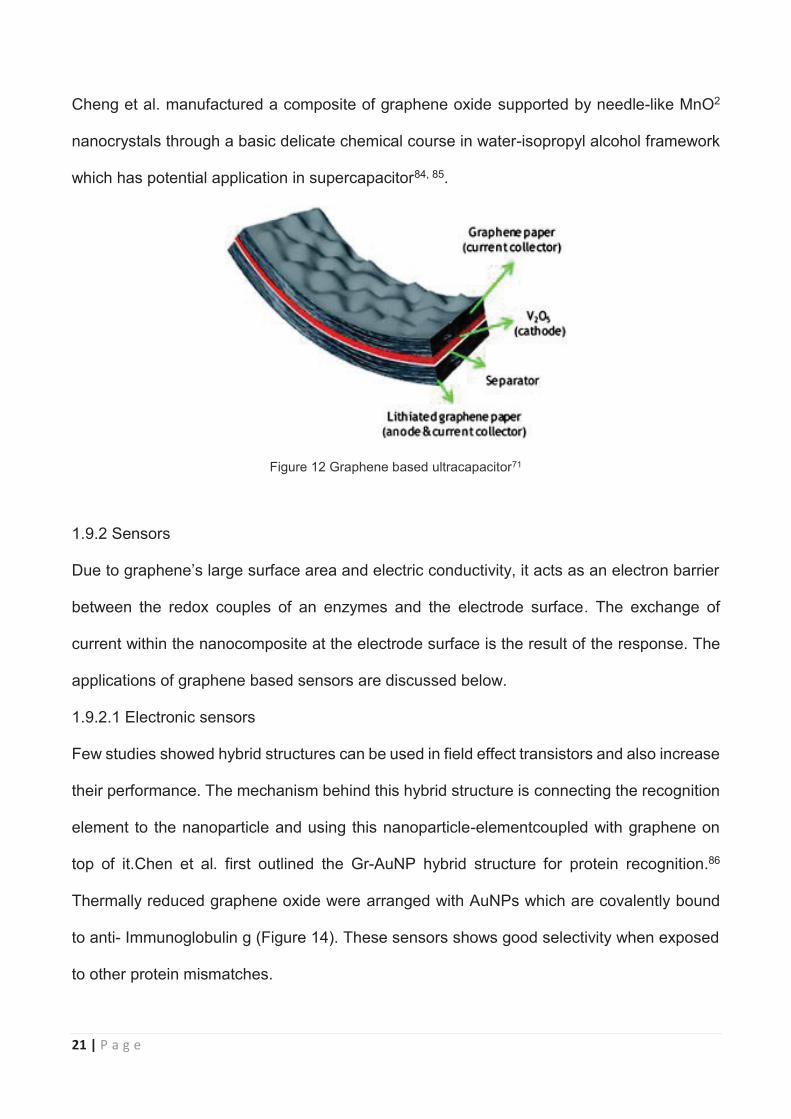
Cheng et al. manufactured a composite of graphene oxide supported by needle-like MnO2
nanocrystals through a basic delicate chemical course in water-isopropyl alcohol framework
which has potential application in supercapacitor84, 85.
Figure 12 Graphene based ultracapacitor71
1.9.2 Sensors
Due to graphene’s large surface area and electric conductivity, it acts as an electron barrier
between the redox couples of an enzymes and the electrode surface. The exchange of
current within the nanocomposite at the electrode surface is the result of the response. The
applications of graphene based sensors are discussed below.
1.9.2.1 Electronic sensors
Few studies showed hybrid structures can be used in field effect transistors and also increase
their performance. The mechanism behind this hybrid structure is connecting the recognition
element to the nanoparticle and using this nanoparticle-elementcoupled with graphene on
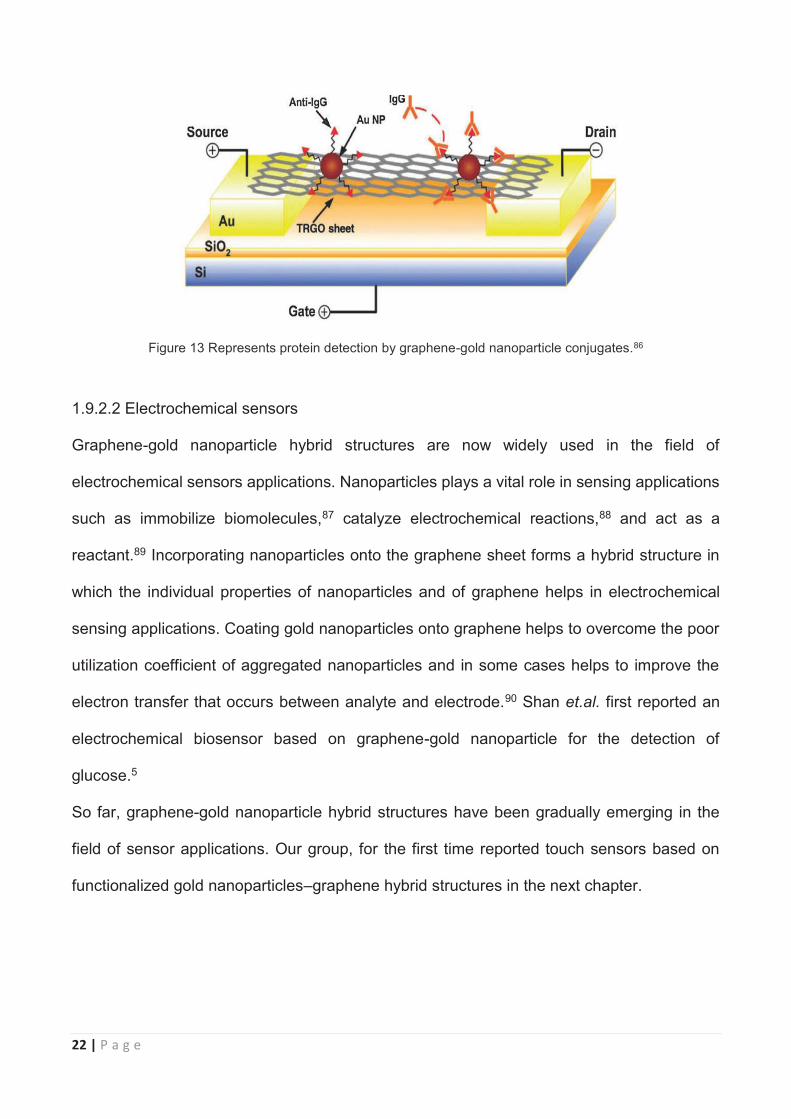
top of it.Chen et al. first outlined the Gr-AuNP hybrid structure for protein recognition.86
Thermally reduced graphene oxide were arranged with AuNPs which are covalently bound
to anti- Immunoglobulin g (Figure 14). These sensors shows good selectivity when exposed
to other protein mismatches.
22 | P a g e
Figure 13 Represents protein detection by graphene-gold nanoparticle conjugates.86
1.9.2.2 Electrochemical sensors
Graphene-gold nanoparticle hybrid structures are now widely used in the field of
electrochemical sensors applications. Nanoparticles plays a vital role in sensing applications
such as immobilize biomolecules,87 catalyze electrochemical reactions,88 and act as a
reactant.89 Incorporating nanoparticles onto the graphene sheet forms a hybrid structure in
which the individual properties of nanoparticles and of graphene helps in electrochemical
sensing applications. Coating gold nanoparticles onto graphene helps to overcome the poor
utilization coefficient of aggregated nanoparticles and in some cases helps to improve the
electron transfer that occurs between analyte and electrode.90 Shan et.al. first reported an
electrochemical biosensor based on graphene-gold nanoparticle for the detection of
glucose.5
So far, graphene-gold nanoparticle hybrid structures have been gradually emerging in the
field of sensor applications. Our group, for the first time reported touch sensors based on
functionalized gold nanoparticles–graphene hybrid structures in the next chapter.
23 | P a g e
1.9.2.3 Biosensors
Graphene is a promising tool in the field of biosensors because of its high sensitivity towards
fluorescent resonance energy transfer [FRET].In recent times, FRET is one of the powerful
tool available for measuring the changes at nano level both in vivo and in vitro91.
Lu et al. reported the first graphene-based biosensor involving a ssDNA that could be bound
and quenched by graphene oxide (GO), with the help of FRET quenching between due to
binding of fluorescently labelled ssDNA with GO92. Jang et al developed a novel GO-based
assay to study the helicase-mediated duplex DNA activity loss. Molecular beacons (MBs) are
unpredictably laid out DNA clasp structures that are double named by a fluorophore and a
quenchor at two ends93. MBs give more grouping specificity than linear probes because of
their dual labelling limits and variable fluorescence which can increase the limit of detection
making it more sensitive; consequently they have been generally utilized as a part of genetic
screening biosensors and biochips, location of single nucleotide polymorphism (SNP) and
mRNA checking in living cells. It has likewise been accounted that GO terminated MB can
identify DNA with higher affectability and single-base mismatch selectivity than routine MB.
Kodali et al. utilized the non-perturbative chemical change of graphene for protein
micropatterning that are pertinent to glucose sensors and cell sensors94. Wang et al. have
used an easy one-stage microwave helped course towards Ni nanosphere/reduced graphene
oxide (rGO) hybrid for non-enzymatic glucose detecting54. Numerous different studies
demonstrated the utilization of graphene and its subsidiaries for the detection of different
biomolecules, for example, amino acids, oligonucleotides, dopamine, adenosine triphosphate
(ATP) thrombin and so forth94, 95.
Alwarappan et al. reported the prompt response of glucose oxidase at an Au electrode
modified with graphene nanosheets96. Feng et al. arranged graphite oxide and graphene by
24 | P a g e
chemical synthesis and connected to alter electrodes in electrochemical identification of
hydroquinone and ascorbic corrosive97.
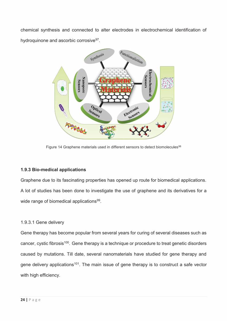
Figure 14 Graphene materials used in different sensors to detect biomolecules98
1.9.3 Bio-medical applications
Graphene due to its fascinating properties has opened up route for biomedical applications.
A lot of studies has been done to investigate the use of graphene and its derivatives for a
wide range of biomedical applications99.
1.9.3.1 Gene delivery
Gene therapy has become popular from several years for curing of several diseases such as
cancer, cystic fibrosis100. Gene therapy is a technique or procedure to treat genetic disorders
caused by mutations. Till date, several nanomaterials have studied for gene therapy and
gene delivery applications101. The main issue of gene therapy is to construct a safe vector
with high efficiency.
25 | P a g e
Liu et.al; and Chen et al reported that polyethylenimine (PEI) when grafted to other framework
diminishes the transfection proficiency, however PEI altered graphene oxide turned out to be
a promising contender for productive gene transfer102. Kim et al. built up a GO based effective
hybrid gene transfer through the establishment of low atomic weight branched
polyethylenimine (BPEI) a cationic polymer, which has been broadly utilized as a proficient
nonviral gene transfer vector103. Bao et al. reported the blend of a chitosan based
functionalized (GO-CS) sheets and its applications in gene transfer104.
1.9.3.2 Drug Delivery
Graphene and its derivaties acts as a platform to form nanocarriers for drug delivery
applications. Due to its structural properties such as mechanical strength, large surface area,
abundant oxygen functional groups, it provides good stability, solubility and high
biocompatibility by loading molecules by different approaches99.
In a study conducted by Sundar and Prajapati, carbon nano tube (CNT) and graphene were
found to be fabulous therapeutic agents for biomedical application. These nano particle
surface functionalized with particular biomolecule based drug delivery has driven another
novel course for balancing the pharmacokinetics, pharmacodynamics, biorecognisation and
for expanding the viability of targeted drugs105. These new measures would minimize the
degradation of drugs and will increase the drug accessibility. Wen and his colleagues showed
the joining of PEG shell has a huge diffusion barrier that antagonistically influences the arrival
of loaded drug and along these lines utilized a redox responsive PEG separation
instrument106. Tahara et al. has explored the accessibility of substantial amounts of single-
walled carbon nanohorns (SWNHs) cytotoxicity and the immunological reactions incited by
the rich uptake level in RAW. 7 murine macrophases, that resulted in apoptosis and death of
26 | P a g e
cells107. Rana et al. reported the drug deliveries of ibuprofen by utilizing a chitosan grafted
GO and controlled its discharge by altering of pH qualities108.
1.9.3.3 Tissue Engineering
Dikin et.al; shown that GO sheets scattered in water can assembled into an ordered structure
under a directional stream, yielding ultra-solid GO or rGO paper. This graphene paper was
utilized for culturing mouse fibroblast cell line (L929) and the outcomes affirmed graphene as
a possibility for adhesion and multiplication of L929 cells109.
Ryoo et.al; studied the behavior of NIH-3T3 fibroblast cells on graphene/ CNTs and
suggested high biocompatibility of these nanomaterials especially as surface coating
materials for implants without inducing notable deleterious effects while enhancing some of
the cellular functions. Lim and his co-workers studied the fabrication and characterization of
graphene hydrogel and its suitability in tissue engineering applications110. Many other
researchers have exploited the properties of graphene for its use in the field of tissue
engineering.
Ryoo et.al; contemplated the behavior of NIH-3T3 fibroblast cells on graphene/CNTs and
recommended high biocompatibility of these nanomaterials particularly as surface covering
materials for inserts without actuating remarkable deletion effects while upgrading a portion
of the cellular operations. Lim and his colleagues concentrated on the synthesis of graphene
hydrogel and its suitability in tissue engineering applications. Numerous different researchers
have explored the properties of graphene for its utilization in the field of tissue engineering110.
1.9.3.4 Cancer Therapy
Because of the distinct conjugated structure, high surface area and low costs, graphene has
opened a new opportunity in the pharmacological applications discipline, in both in-vitro and
27 | P a g e
in-vivo. Graphene and its associated compounds have been utilized for different biomedical
applications which comprises of anti-cancer therapy111. Studies conducted by Yang et.al;
showed in-vivo tumor uptake and effective photothermal therapy by intravenous injection of
PEGylated nano graphene sheets (NGS) in different xenograft mouse model111. Shen and
his colleagues have utilized the multi operational nanocomposite dependent on graphene
oxide (GO) for in-vitro hepatocarcinoma treatment and diagnosis99.
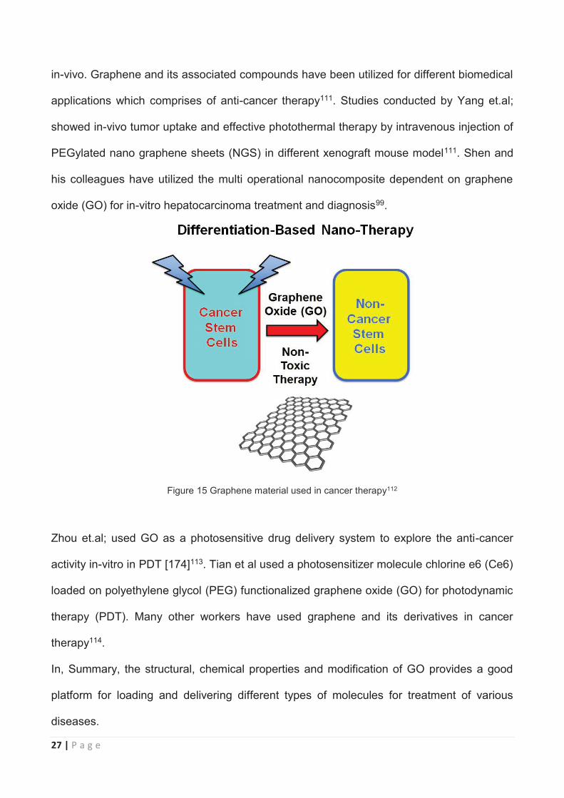
Figure 15 Graphene material used in cancer therapy112
Zhou et.al; used GO as a photosensitive drug delivery system to explore the anti-cancer
activity in-vitro in PDT [174]113. Tian et al used a photosensitizer molecule chlorine e6 (Ce6)
loaded on polyethylene glycol (PEG) functionalized graphene oxide (GO) for photodynamic
therapy (PDT). Many other workers have used graphene and its derivatives in cancer
therapy114.
In, Summary, the structural, chemical properties and modification of GO provides a good
platform for loading and delivering different types of molecules for treatment of various
diseases.
28 | P a g e
CHAPTER 2 – Materials & Methods
2.1 Synthesis of AuNPs AuNPs with diameters of 13nm, 45nm, 75nm and 100 nm were synthesized according to the
literature115. A stock solution of 5.0 x 10⁻³ M HAuCl4 was made by dissolving Gold (III) chloride
trihydrate (HAuCl4·3H2O, 99.9 + % metals basis, Sigma) in deionized water. 1 ml of as
prepared HAuCl4 was added to 18 ml of boiling water followed by addition of 0.5% (w/w)
sodium citrate tribasic dehydrate (C6H5Na3O7·2H2O, 99%, Sigma). As the volume of sodium
citrate determines the size of the AuNPs, different volumes were used for different size
AuNPs. Typically, in order to prepare 13nm, 45nm, 75nm and 100nm size AuNPs, aliquots
of 1000 μl, 365 μl, 200 μl and 150 μl volumes of sodium citrate were added, respectively. The
solution was continuously stirred until the change in color was observed. The solution was
carefully removed from the hot plate and was cooled by stirring atroom temperature. The
characterization was done by UV-Visible Spectroscopy and transmission electron
microscopy (TEM).
2.1.2 Surface Functionalisation of AuNPs
AuNPs were functionalised with cystamine sulfate hydrate (98% sigma aldrich), a short
bifunctional molecule. Addition of cystamine to AuNPs induces rapid aggregation. The
functionalisation of AuNPs with short bifunctional molecule is based on Au-S (gold and
sulphur) bond with cystamine as a sulphur containing bifunctional molecule. After addition of
250 μl of 0.1 M cystamine solution to 5 ml of AuNPs an immediate change of color was
observed from red to blue. The reduction was characterised by using UV-Vis spectroscopy
and conductance was measured using a multimeter (Digitech, QM1549, Aus).
2.1.3 Hybrid Film Preparation
Functionalized AuNPs (2 ml) was added to Gr (1mg/ml) solution (2 ml) and incubated for 10
mins with care being taken to prevent aggregation. Graphene and AuNPs films were
29 | P a g e
fabricated by layer by layer (LBL) assembly using an isoporous membrane (polycarbonate,
hydrophilic, 0.2 μm, 25mm, white, plain, Millipore Corporation, Australia). Typically, 2 ml of
graphene was used as the first layer followed by 2 ml of functionalised AuNP’s and finally 2
ml of graphene was added as a top layer. After adding each layer the solution was vacuum
filtered and made into thin film before addition of other layers. Another set of films were
prepared from a mixed solution of graphene and functionalized AuNPs. The film was then air
dried under fume hood for 10 mins and carefully peeled off from the membrane, to have a
free standing film. As such prepared films were used for Raman and FTIR spectroscopy
characterization.Sensitivity tests was performed by placing the sheet onto the gold electrode,
with care being taken to prevent breaking of sheet.
2.1.4 Preparation of CRGOs
Preparation of CRGOs, L-ascorbic acid was added GO solution(1mg/mL) in 10:1 ratio
followed by addition of ammonia and subjected to continuous stirring at different time
intervals, which involves high speed centrifugation. These CRGOs were then dispersed in
DMF solvent (1mg/ml).
2.1.5 Stepwise preparation of various CRGOs modified gold electrode
Au electrode was polished with fine alumina powders (1 and 0.05 μm) on the polishing cloth,
and then the electrode was rinsed with double distilled water followed by ethanol in an
ultrasonic bath for 5 mins, and finally rinsed with double distilled water. Then the electrode
was electrochemically cleaned by consecutive potential cycling between -0.5 to +2.0 at 100
mV/s in 1 MH2SO4 until a characteristic cyclic voltammogram of a clean Au surfacewas
obtained.
SAM modified Au electrodes were prepared by incubating the electrode in 10 mM solution of
respective alkanethiol in ethanol for 24 hrs at room temperature. The electrode was rinsed
with ethanol and dried under nitrogen atmosphere.
30 | P a g e
Subsequently, the immobilization of CRGO’s on the SAM surface was achieved by dipping
the electrode into CRGOs dispersion in DMF (1mg/mL). Sufficient time of dipping is required
to get a proper binding of CRGO on to the SAM electrode. Then the electrode was rinsed
with DMF followed by double distilled water to remove the unbound CRGO’s and then dried
under nitrogen atmosphere before running the experiment.
2.2 Instrumentation, Acquisition Parameters and Sample Preparation
2.2.1 UV-Visible Spectroscopy (UV-Vis)
All the scans was performed in a continuous mode from 800nm to 200 nm using quartz
cuvette of path length 1mm, with a scan rate of 500 nm/min and data interval of 1 nm using
Varian, Cary 300 model. 1 mg/ml of Gr and functionalized AuNPs +Gr solution were used for
the measurements.
2.2.2 Attenuated Total reflection Fourier Transform Infra Red (ATR-FTIR)
FTIR was performed using Alpha FTIR spectrometer( Bruker Optik GmbH,Ettlingen,
Germany) equipped with a deuteraed triglycine sulphate (DTGS) detector and a single
reflection diamond ATR sampling module (Platinum ATR quick-Snaptm). Spectral resolution
4cm-1 with 256 co-added scans were used. Background measurements were obtained before
scanning each sample.
2.2.3 Raman Spectroscopy
Measurements were conducted using Renishaw Invia Raman Microspectrometer (Reinshaw
pls, Gloucestershire, UK), equipped with 514nm laser and a thermo-electrical cooled CCD
detector. Spectral data was acquired using 20s exposure time together with 4cm-1 spectral
resolution. Further analysis was performed using OPUS 6.0 software suite.
31 | P a g e
2.2.4 Scanning Electron Microscopy (SEM)
For SEM imaging purpose, Supra 55VP from Carl ZEISS (Germany) uses Schottky-type field-
emission electron source. Imaging was performed at 0.02-30 kV acceleration voltage, 1.6nm
at 1kV resolution and magnification between 12-1,000,000 x and with variable pressure of 2-
133pa.
2.2.5 Transmission Electron Microscopy (TEM)
For TEM imaging purpose, JEM 2100 Lab6 TEM from JEOL (JEOL USA, Inc.) was used
equipped with Lanthanum Hexaboride (Lab6) as electron source. Scans were performed at
HT of 200 kV, 50-6,000x for lower magnification range and 2,000-1,500,000x for higher
magnification range.Samples were prepared by dropping them onto the carbon grid and
subjected to drying for 3 hours.
2.2.6 Potentiostat
Cyclic Voltammetry and Chronoamperometry were performed using Potentiostat
(Bioanalytical Systems Inc, U.S.A). All scans were performed with a scan rate 0-100 (mV/s),
potential range from 0-1000 mV and time range from 1-65 secs. Further analysis was
performed by Origin software.
2.2.7 Electrochemical measurements
The cyclic voltammetric (CV) measurements of the gold modified electrodes were recorded
using a 10 mM Fe(CN)63- solution in 0.1 M KCl at the cycling potential between –0.1 and 0.4
V vs. Ag/AgCl (scan rate: 100 mV/s). For impedance studies, 10 mV of amplitude of the
electrode and potential of the redox couple (0.2 V) was conducted with the frequency range
between 105 and 10-2 Hz. The ZSimp-Win program was used to calculate the electrochemical
impedance spectroscopy (EIS) data to determine the optimized values for the charge transfer
resistances.

32 | P a g e
For impedance studies, 10 mV of amplitude of the electrode and potential of the redox couple
(0.2 V) was conducted with the frequency range between 105 and 10-2 Hz. The ZSimp-Win
program was used to calculate the electrochemical impedance spectroscopy (EIS) data to
determine the optimized values for the charge transfer resistances.
33 | P a g e
Chapter 3 - Graphene based hybrid actuator for the potential application of artificial muscle
3.1 Introduction
Actuators are mechanical machines, which can transform one form of energy into another
form of energy under different external stimuli116. Under the different external stimuli,
actuators can serve as a transformational unit, which undergoes mechanical deformation due
to change in volume, which corresponds to a change of other stimuli into mechanical
energy42. This stimulus can be current, heat, light and temperature based on the actuation
mechanisms and supply of energy44.
Actuators have a wide range of applications, including medical devices117, switches118,
microrobotics119, and sensors120. Generally, the actuator material comprises of conducting
materials, polymers, and carbon-based materials44. Previously, a wide extent of inorganic
materials, comprising of shape memory alloys and piezoelectric ceramics has been
investigated as actuators121, 122. Though, the need of high intensity of heat inhibits their extent
of applications123. On the other hand, polymer based soft actuators such as conjugated
polymers and the polymer gels have benefits like flexibility, lightweight, transparency and
their long life span, but their short response time and poor energy conversion restricts the
efficiency of these polymer based actuators42, 83, 95.
Furthermore, most of the polymer dependent materials need post processing steps which
does not go hand in hand with fabrication steps. Clearly, actuator materials have various
benefits such as cost effective, response time, accuracy and device designing and
restrictions such as potential range and detection time42, 124. Thus, it still remains a challenge
to develop actuatorswith quick response time at lower potential difference, together with
design of well-suited assembly process125. Carbon-based materials, comprising carbon
nanotubescan provide actuation with the high stress results and efficacy at low potential, but
34 | P a g e
with low shear output126. Because of their distinctive structure and their superior aspects,
therehave been reports demonstrating the application of single walled carbon nanotubes
(SWCNT) for electromechanical actuators that can produce stresses which are higher than
that of natural muscles and produce excellent strain at lower voltages127-129.
Earlier, carbon nanotube (CNT) based actuators have grabbed lot of attention due to its
surface area and mechanical properties and charge transfer characteristics130, 131. Recently
single walled carbon nanotubes (SWCNTs) and multiwalled carbon nanotubes (MWCNTs)
are reported as actuators.132-134 Park et.al; demonstrates GO/MWCNT bilayer actuator curled
into various directions due to different temperature conditions44. The main drawback for this
type of actuators are 1) they are highly temperature dependent which may affect the response
of the actuator. Raguse et.al; demonstrated the actuators which were fabricated with gold
nanoparticles functionalised with short bifunctional molecules such as cystamine
hydrochloride. The limitations of this system are 1) the functionalised AuNP electrode is
dependent on substrate, which effects the deflection of actuator, 2) they did not focus on the
stability of the functionalised AuNP electrode, which plays an important role in actuator
applications.
Graphene hybrid materials could be used to overcome the above limitations and also to
satisfy the potential conditions such as high porosity, highly conductivity, high mechanically
strength, flexibility and the ability to move forward and backward which is essential for an
actuator. Graphene (Gr), a single layer carbon atoms arranged in a honeycomb like crystal
structure, with its extraordinary and unique properties, is in the limelight of researchers for
applying them as a actuation material135. Due to its mechanical strength, electrical
conductivity, large surface area and flexibility there employment as actuation material could
result in high quality actuator material136-138. To enhance the actuator performance,
functionalised AuNPs was sandwiched between two graphene layers as an
35 | P a g e
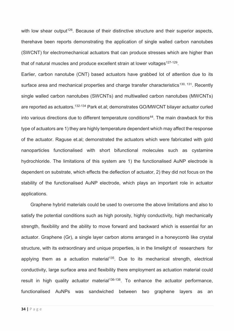
electromechanical graphene hybrid actuator. The self-assembly and the layer by layer
assembly can be clearly demonstrated in the pictorial representation by using VMD software
(shown in the figure 16). This results in improved deflection of the actuator material.
Chronoamperometry and cyclic voltammetry was used to study the response and stability of
actuator.
Figure 16 Represents the self-assembly of hybrid graphene film (Mahesh, Visual Molecular Dynamics).
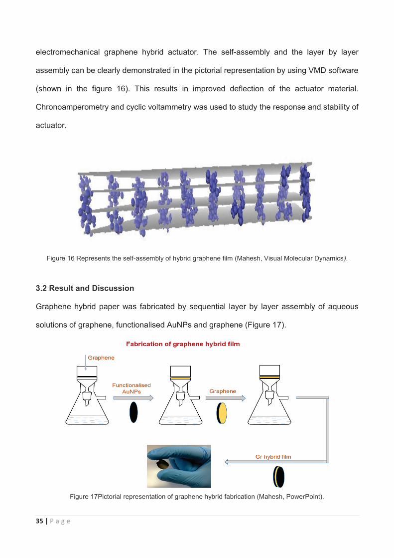
3.2 Result and Discussion
Graphene hybrid paper was fabricated by sequential layer by layer assembly of aqueous
solutions of graphene, functionalised AuNPs and graphene (Figure 17).
Figure 17Pictorial representation of graphene hybrid fabrication (Mahesh, PowerPoint).
36 | P a g e
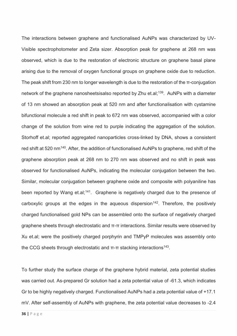
The interactions between graphene and functionalised AuNPs was characterized by UV-
Visible spectrophotometer and Zeta sizer. Absorption peak for graphene at 268 nm was
observed, which is due to the restoration of electronic structure on graphene basal plane
arising due to the removal of oxygen functional groups on graphene oxide due to reduction.
The peak shift from 230 nm to longer wavelength is due to the restoration of the π-conjugation
network of the graphene nanosheetsisalso reported by Zhu et.al;139. AuNPs with a diameter
of 13 nm showed an absorption peak at 520 nm and after functionalisation with cystamine
bifunctional molecule a red shift in peak to 672 nm was observed, accompanied with a color
change of the solution from wine red to purple indicating the aggregation of the solution.
Storhoff et.al; reported aggregated nanoparticles cross-linked by DNA, shows a consistent
red shift at 520 nm140. After, the addition of functionalised AuNPs to graphene, red shift of the
graphene absorption peak at 268 nm to 270 nm was observed and no shift in peak was
observed for functionalised AuNPs, indicating the molecular conjugation between the two.
Similar, molecular conjugation between graphene oxide and composite with polyaniline has
been reported by Wang et.al;141. Graphene is negatively charged due to the presence of
carboxylic groups at the edges in the aqueous dispersion142. Therefore, the positively
charged functionalised gold NPs can be assembled onto the surface of negatively charged
graphene sheets through electrostatic and π-π interactions. Similar results were observed by
Xu et.al; were the positively charged porphyrin and TMPyP molecules was assembly onto
the CCG sheets through electrostatic and π-π stacking interactions143.
To further study the surface charge of the graphene hybrid material, zeta potential studies
was carried out. As-prepared Gr solution had a zeta potential value of -61.3, which indicates
Gr to be highly negatively charged. Functionalised AuNPs had a zeta potential value of +17.1
mV. After self-assembly of AuNPs with graphene, the zeta potential value decreases to -2.4
37 | P a g e
mV when compared to graphene. Addition of functionalised AuNPs to the graphene resulted
in the formation of stable colloids which could be attributed to electrostatic interactions. Li
et.al; justified the stability of GO colloidals of aqueous dispersions to be due to electrostatic
stabilization of graphene sheets142.
Figure 18 Surface properties: a) UV-Vis for Gr, AuNPs, AuNPs coated cystamine and Gr-AuNPs coated
cystamine. b) Zeta potential Gr and Gr-functionalised gold NPs in aqueous dispersion.
The morphological structure of graphene hybrid paper were characterized by scanning
electron microscope (SEM) as shown in Figure 19. The cross-section of the graphene hybrid
sheet has broken edges, which indicates graphene and functionalised gold NPs are arranged
layer by layer with well order structure during fabrication process130. Yongshen Chen et.al;
demonstrated graphene/Fe3O4 hybrid paper as an electrochemical actuator, were in fractured
sheet indicates well-ordered layered structure43.
a b
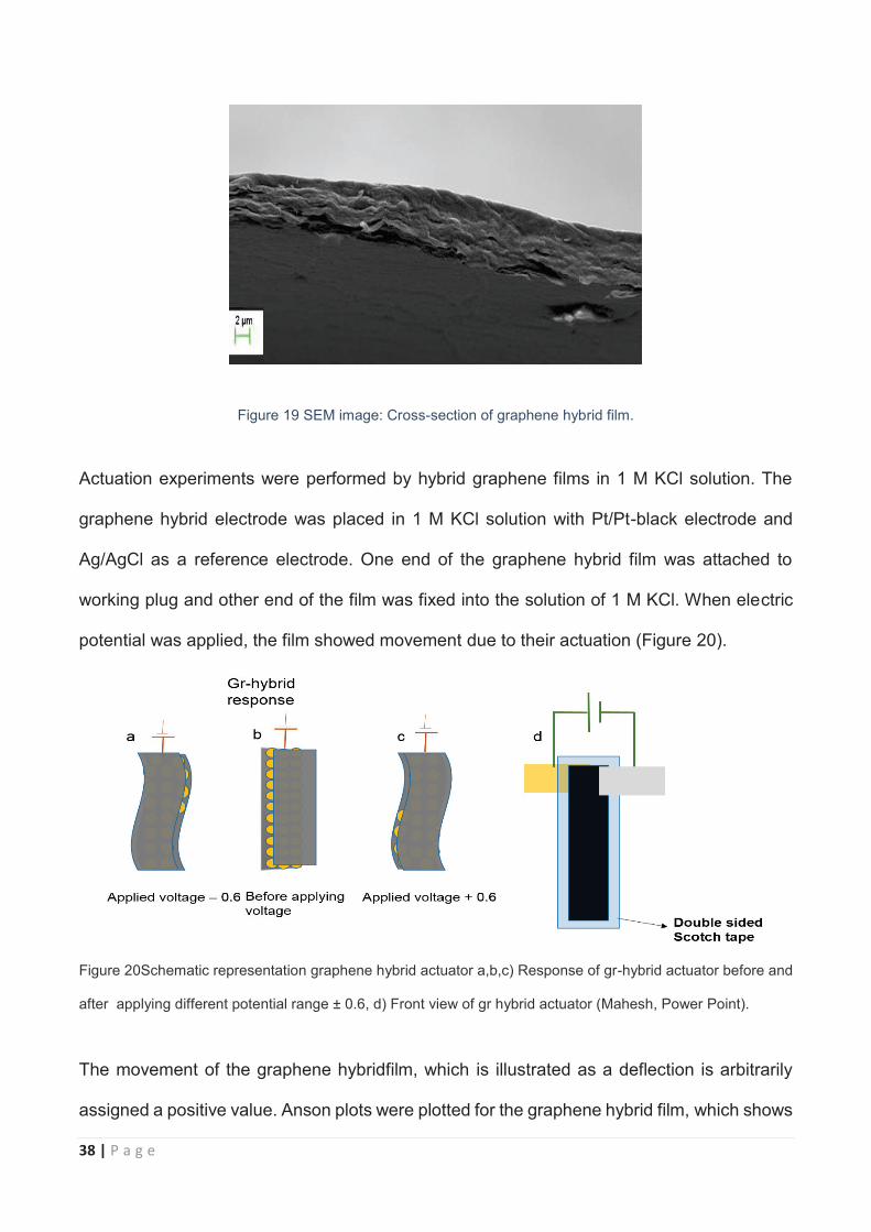
38 | P a g e
Figure 19 SEM image: Cross-section of graphene hybrid film.
Actuation experiments were performed by hybrid graphene films in 1 M KCl solution. The
graphene hybrid electrode was placed in 1 M KCl solution with Pt/Pt-black electrode and
Ag/AgCl as a reference electrode. One end of the graphene hybrid film was attached to
working plug and other end of the film was fixed into the solution of 1 M KCl. When electric
potential was applied, the film showed movement due to their actuation (Figure 20).
Figure 20Schematic representation graphene hybrid actuator a,b,c) Response of gr-hybrid actuator before and
after applying different potential range ± 0.6, d) Front view of gr hybrid actuator (Mahesh, Power Point).
The movement of the graphene hybridfilm, which is illustrated as a deflection is arbitrarily
assigned a positive value. Anson plots were plotted for the graphene hybrid film, which shows
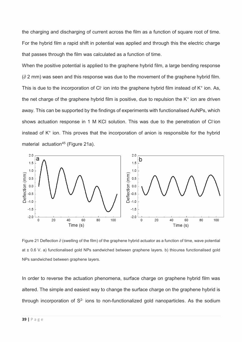
39 | P a g e
the charging and discharging of current across the film as a function of square root of time.
For the hybrid film a rapid shift in potential was applied and through this the electric charge
that passes through the film was calculated as a function of time.
When the positive potential is applied to the graphene hybrid film, a large bending response
(∂ 2 mm) was seen and this response was due to the movement of the graphene hybrid film.
This is due to the incorporation of Cl- ion into the graphene hybrid film instead of K+ ion. As,
the net charge of the graphene hybrid film is positive, due to repulsion the K+ ion are driven
away. This can be supported by the findings of experiments with functionalised AuNPs, which
shows actuation response in 1 M KCl solution. This was due to the penetration of Cl-ion
instead of K+ ion. This proves that the incorporation of anion is responsible for the hybrid
material actuation45 (Figure 21a).
Figure 21 Deflection ∂ (swelling of the film) of the graphene hybrid actuator as a function of time, wave potential
at ± 0.6 V. a) functionalised gold NPs sandwiched between graphene layers. b) thiourea functionalised gold
NPs sandwiched between graphene layers.
In order to reverse the actuation phenomena, surface charge on graphene hybrid film was
altered. The simple and easiest way to change the surface charge on the graphene hybrid is
through incorporation of S2- ions to non-functionalized gold nanoparticles. As the sodium
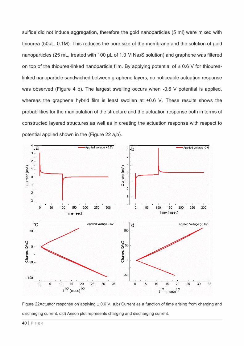
40 | P a g e
sulfide did not induce aggregation, therefore the gold nanoparticles (5 ml) were mixed with
thiourea (50μL, 0.1M). This reduces the pore size of the membrane and the solution of gold
nanoparticles (25 mL, treated with 100 μL of 1.0 M Na2S solution) and graphene was filtered
on top of the thiourea-linked nanoparticle film. By applying potential of ± 0.6 V for thiourea-
linked nanoparticle sandwiched between graphene layers, no noticeable actuation response
was observed (Figure 4 b). The largest swelling occurs when -0.6 V potential is applied,
whereas the graphene hybrid film is least swollen at +0.6 V. These results shows the
probabilities for the manipulation of the structure and the actuation response both in terms of
constructed layered structures as well as in creating the actuation response with respect to
potential applied shown in the (Figure 22 a,b).
Figure 22Actuator response on applying ± 0.6 V. a,b) Current as a function of time arising from charging and
discharging current. c,d) Anson plot represents charging and discharging current.
a b
c d
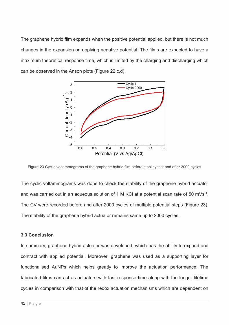
41 | P a g e
The graphene hybrid film expands when the positive potential applied, but there is not much
changes in the expansion on applying negative potential. The films are expected to have a
maximum theoretical response time, which is limited by the charging and discharging which
can be observed in the Anson plots (Figure 22 c,d).
Figure 23 Cyclic voltammograms of the graphene hybrid film before stability test and after 2000 cycles
The cyclic voltammograms was done to check the stability of the graphene hybrid actuator
and was carried out in an aqueous solution of 1 M KCl at a potential scan rate of 50 mVs-1.
The CV were recorded before and after 2000 cycles of multiple potential steps (Figure 23).
The stability of the graphene hybrid actuator remains same up to 2000 cycles.
3.3 Conclusion
In summary, graphene hybrid actuator was developed, which has the ability to expand and
contract with applied potential. Moreover, graphene was used as a supporting layer for
functionalised AuNPs which helps greatly to improve the actuation performance. The
fabricated films can act as actuators with fast response time along with the longer lifetime
cycles in comparison with that of the redox actuation mechanisms which are dependent on

42 | P a g e
the electrochemical doping of conducting polymers. The graphene hybrid results in the
actuation, when positive or negative potential is applied based on the surface charge. The
graphene hybrid actuators are simple to fabricate, uses lower voltage (< 0.6 V) for actuation,
and have a faster response time (<0.5 s). Furthermore, the graphene hybrid actuator has an
improved stability and the performance of the actuator remains same even after 1500 cycles
of actuation. These graphene hybrid actuator could be employed for future applications in
artificial muscles, robotics, micro-electromechanical machines (MEMs) and nano-
electromechanical machines (NEMs).
43 | P a g e
CHAPTER 4 - Highly sensitive pressure sensor based on graphene hybrids
4.1 Introduction
Gold nanoparticles are the most stable and unique particles compared with other metal
nanoparticles such as Ag, Pd with many applications related to sensors144, 145 and biological
systems146, 147.Moreover, to control the surface properties and interaction nature between the
hybrid structures,the sizes and shapes of the nanoparticles should be considered148, 149. The
ease of synthesis and functionalisation of different sizes of AuNPsmakes it more emanate.
AuNPs can be functionalized with different types of molecular ligands,such as
alkanethiolates, enzymes, DNA, proteins, sugars, oligonucleotides, phospholipids and
more150-152. In case of sensor applications, functionalised nanoparticles can be synthesised
with other materials with various physical and chemical functions, which has an impact on
the sensitivity and selectivity of the sensor. The assembly of functionalized AuNPs requires
a suitable platform exhibit unique properties153.Graphene and its hybrid materials have been
used presently, in the development of high performance sensors, as advanced systems
because of their large surface area, conductivity and ability for immobilization of enzymes17,
154, 155.Especially, the carboxylic groups present at the edge of the graphene could be
functionalised with other materials by 1-ethyl-3-(3-dimethylaminopropyl)- carbodiimide
(EDC)156 or thionyl chloride (SOCl2)157, 158. The non-covalent interactions are the weak
interactions between graphene and other molecules. For example Li et.al; reported MP-11
non-covalently functionalised on graphene159.
Increase in demand for portable sensors has lead for the development of sophisticated
sensors. Graphene acts as a potential candidate for the development of well-defined
structures due to its large surface area, electrical and mechanical properties.
Functionalisation with other materials could lead to development of sensors with properties
44 | P a g e
which is not easily obtainable16. Selectivity and sensitivity can be significantly increased by
coupling with a sensing component. In case of graphene hybrid sensor, the sensing
components can vary from metal oxides, metal NPs and biomolecules16. Herrmann et.al; was
first to demonstrate the functionalised gold NP-based sensitive strain gauges for sensor
applications. The study mainly focuses on tunneling model and sensitivity of the
functionalised NP films, which depends on various factors like size of the nanoparticle,
interparticle distance, and the conductance of the binding molecules. The drawbacks of this
system were 1) the sensitivity and detection range of weight was not varied based on suitable
applications. 2) the properties of NP-based sensors mainly dependent on substrate and the
linker molecules. Shu Gong et.al; reported a wearable and highly sensitive pressure sensor
with ultrathin gold nanowires which was able to show fast response time (<17 ms), high
sensitivity (1.14 kPa-1) and high stability160. The flaws with this system were 1) impregnation
of AuNWs on to tissue paper and sandwiched between PDMS instead of using only AuNW
2) it shows a high resistance of 2.5 ± 0.4 MΩ sq-1 which is not suitable for a sensor. To
overcome these problems, we designed a new device with higher sensitivity factor and well
organized structure. Herein, we show that functionalised gold NPs could be sandwiched
between two graphene layers, leading to a novel pressure sensor (shown in Figure24). The
advantage of using graphene hybrid is its sensing mechanism and its excellent electronic
and electrochemical properties of this material which helps to improve the sensitivity. When
compared with previous reports, our graphene hybrid device shows good sensitivity. It is
mandatory for the surface to be uniform and have good transfer of electrons for checking the
sensitivity of a device, the film fabricated here is free standing which fulfills both the
prerequisite mentioned above. This novel device shows good performance witha sensitivity
of 0.0009mN-1.
45 | P a g e
Figure 24 Pictorial representation of the hybrid film (Mahesh, PowerPoint)
4.2 Results and Discussion
A hybrid film with graphene and functionalised AuNPswas successfully fabricated using
vacuum filtration. The film shows good conductivity with widerange of pressure sensitive
responses. Surface morphology of the film was studied by SEM and TEM. Figure 25shows
the SEM image of layer-by-layer assembly of a graphene hybrid film. As the pressure
increases the layers were tightly packed one on top of the other and forms a compactfilm with
a thickness of 572nm. Figure 25b shows the layer by layer deposition of functionalised gold
NPs sandwiched between graphene layers. The cause for wrinkling of the film may be due
to the electrostatic interactionsbetween the functionalized gold NPs and the graphene layers
and the surface roughness of the film during surface compression, which increases with
increase in number of layers161, 162.
46 | P a g e
Figure 25SEM images a.) Cross-section of Gr hybrid film b.) Shows side view for Gr hybrid film.
Figure 26 a shows transmission electron microscope (TEM) image of the shape and size of
functionalised gold nanoparticles. The structure could be characterized as chain like structure
after functionalised with cystamine with an average particle size of 17 ± 3 nm,which is the
key for designing sensitive devices.Figure 26b shows the binding of functionalized gold
nanoparticles on the graphene sheets, which results in continuous flow of electrons which
can affect the resistance of the material.163The functionalised AuNPs are well dispersed on
the graphene sheets. The functionalized AuNPs are uniform in size on the graphene sheet.
Once the morphology studies were conducted, the structural characterization with respect to
functional groups were characterised by Raman and FTIR spectroscopy.
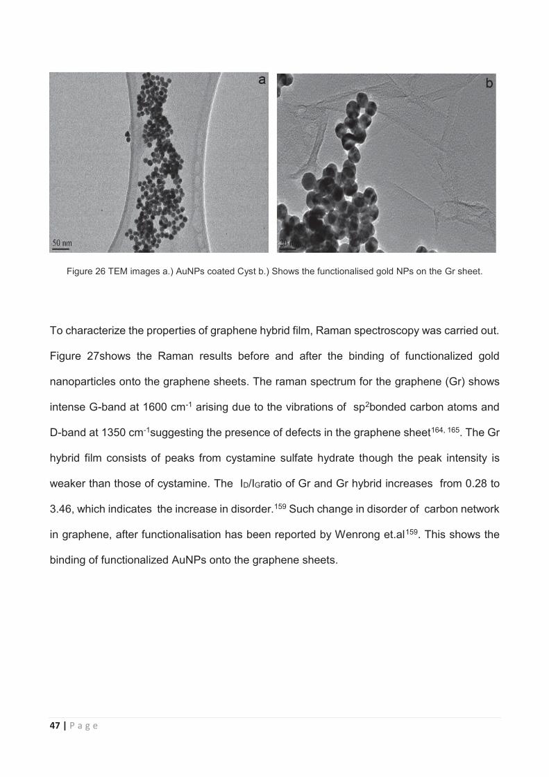
47 | P a g e
Figure 26 TEM images a.) AuNPs coated Cyst b.) Shows the functionalised gold NPs on the Gr sheet.
To characterize the properties of graphene hybrid film, Raman spectroscopy was carried out.
Figure 27shows the Raman results before and after the binding of functionalized gold
nanoparticles onto the graphene sheets. The raman spectrum for the graphene (Gr) shows
intense G-band at 1600 cm-1 arising due to the vibrations of sp2bonded carbon atoms and
D-band at 1350 cm-1suggesting the presence of defects in the graphene sheet164, 165. The Gr
hybrid film consists of peaks from cystamine sulfate hydrate though the peak intensity is
weaker than those of cystamine. The ID/IGratio of Gr and Gr hybrid increases from 0.28 to
3.46, which indicates the increase in disorder.159 Such change in disorder of carbon network
in graphene, after functionalisation has been reported by Wenrong et.al159. This shows the
binding of functionalized AuNPs onto the graphene sheets.
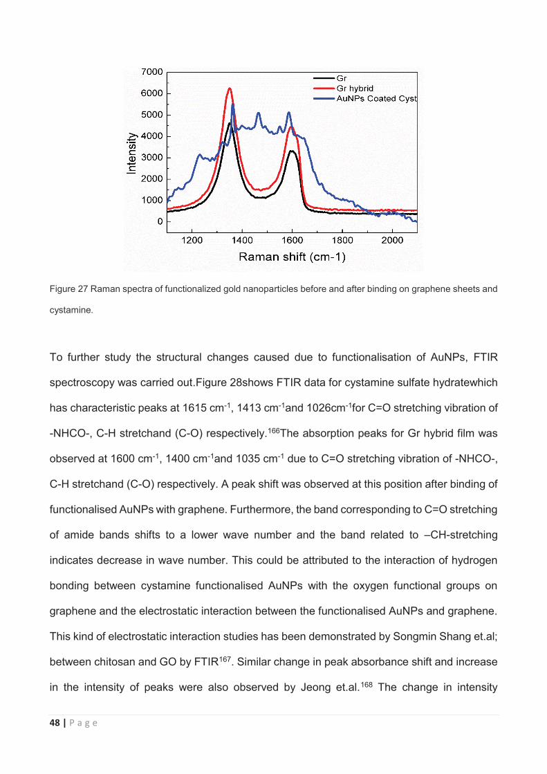
48 | P a g e
Figure 27 Raman spectra of functionalized gold nanoparticles before and after binding on graphene sheets and
cystamine.
To further study the structural changes caused due to functionalisation of AuNPs, FTIR
spectroscopy was carried out.Figure 28shows FTIR data for cystamine sulfate hydratewhich
has characteristic peaks at 1615 cm-1, 1413 cm-1and 1026cm-1for C=O stretching vibration of
-NHCO-, C-H stretchand (C-O) respectively.166The absorption peaks for Gr hybrid film was
observed at 1600 cm-1, 1400 cm-1and 1035 cm-1 due to C=O stretching vibration of -NHCO-,
C-H stretchand (C-O) respectively. A peak shift was observed at this position after binding of
functionalised AuNPs with graphene. Furthermore, the band corresponding to C=O stretching
of amide bands shifts to a lower wave number and the band related to –CH-stretching
indicates decrease in wave number. This could be attributed to the interaction of hydrogen
bonding between cystamine functionalised AuNPs with the oxygen functional groups on
graphene and the electrostatic interaction between the functionalised AuNPs and graphene.
This kind of electrostatic interaction studies has been demonstrated by Songmin Shang et.al;
between chitosan and GO by FTIR167. Similar change in peak absorbance shift and increase
in the intensity of peaks were also observed by Jeong et.al.168 The change in intensity
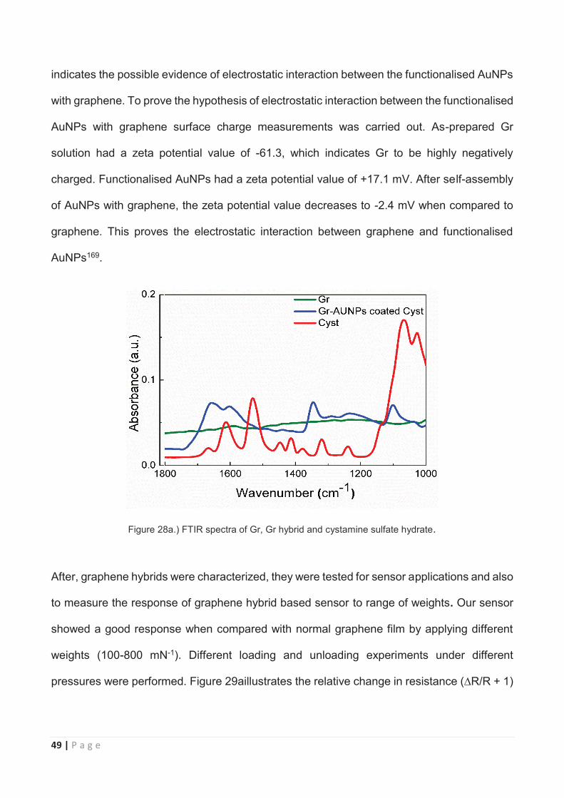
49 | P a g e
indicates the possible evidence of electrostatic interaction between the functionalised AuNPs
with graphene. To prove the hypothesis of electrostatic interaction between the functionalised
AuNPs with graphene surface charge measurements was carried out. As-prepared Gr
solution had a zeta potential value of -61.3, which indicates Gr to be highly negatively
charged. Functionalised AuNPs had a zeta potential value of +17.1 mV. After self-assembly
of AuNPs with graphene, the zeta potential value decreases to -2.4 mV when compared to
graphene. This proves the electrostatic interaction between graphene and functionalised
AuNPs169.
Figure 28a.) FTIR spectra of Gr, Gr hybrid and cystamine sulfate hydrate.
After, graphene hybrids were characterized, they were tested for sensor applications and also
to measure the response of graphene hybrid based sensor to range of weights. Our sensor
showed a good response when compared with normal graphene film by applying different
weights (100-800 mN-1). Different loading and unloading experiments under different
pressures were performed. Figure 29aillustrates the relative change in resistance (∆R/R + 1)
50 | P a g e
as a function of force (F), which shows the sensor sensitivity value of 0.0005 kPa-1 for applied
force of 130 mN-1. Using Eq.1170the sensitivity factor can be calculated.
(1)
Earlier Darren Alvares et.al; reported a sensitivity factor of (SF) of 0.0039 mN-1170 for
functionalised gold nanoparticle based sensor. Shu Gong et.al; demonstrated ultrathin gold
nanowires as a highly sensitive pressure sensor, the sensitivity factor was shown to be 1.14
kPa-1.160 Whereas, our graphene hybrid based sensor shows a high sensitivity factor of
0.0005 kPa-1 which is approximately 2000 times better as compared with above works. This
was due to the exhibition of extrinsic properties from the graphene and functionalised gold
NPs. These sensors have a large surface area, which has more sensitive contact positions
that varies charge transfer when pressure is applied. The device shows controllable pressure
response (change in resistance) with the same applied force (100-800 mN-1) repeatedly and
with a change in response time shown in Figure 29 a. The device was also tested for
sensitivity and compared the response with graphene film as shown in Figure 29 b. The
graphene hybrid based sensor shows stable responses and high sensitivity for tap and
release and weight press applications with a quicker response time of less than 10 ms. After
the addition of functionalised AuNPs to graphene, the graphene hybrid based sensor shows
increase in sensitivity when compared to normal graphene film.Further, the sensitivity was
tested for tap and release function. High signal to noise ratio were observed in the force
measurement, indicating the higher sensitivity of our graphene hybrid sensor as shown in
Figure 29 C. The graphene hybrid device shows a stable response for tap and release test.
Although the bandwith and line shape was nearly unaltered as the load frequency increased,a
quick response time of <15 ms was observed in the unloading process. Figure 29 d shows
the response of the device upon applying two different forces, the response time and
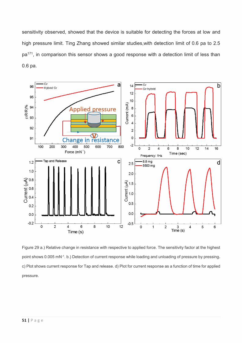
51 | P a g e
sensitivity observed, showed that the device is suitable for detecting the forces at low and
high pressure limit. Ting Zhang showed similar studies,with detection limit of 0.6 pa to 2.5
pa171, in comparison this sensor shows a good response with a detection limit of less than
0.6 pa.
Figure 29 a.) Relative change in resistance with respective to applied force. The sensitivity factor at the highest
point shows 0.005 mN-1. b.) Detection of current response while loading and unloading of pressure by pressing.
c) Plot shows current response for Tap and release. d) Plot for current response as a function of time for applied
pressure.

52 | P a g e
4.3 Conclusion
In summary, we have successfully developed a novel method for fabricating high sensitive
sensors by self-assembly of functionalised AuNPs between two graphene layers. The flexible
graphene hybrid based sensor, was constructed by layer by layer deposition of graphene
followed by functionalised AuNPs and graphene layers. Higher sensitivity was achieved to
mimic the natural touch senses. It provides a facile synthesis method for fabrication of hybrid
films which could be applied for flexible and high sensitive devices with very low cost of
production. The graphene hybrid based sensor demonstrated high sensitivity for detection of
minute forces together with fast response time and high stability. This novel device shows a
high sensitivity factor of 0.0005 mN-1, with a fast response time of < 15 ms which shows a
better sensitivity compared to previous reports160, 170. With this graphene hybrid sensor, we
could detect loads in a pressure range of (0.086 mN-1 to 53.9 mN-1 with corresponding to
applications like tap and release. The relative resistance of the films to the applied force is
consistent, which is due to electron tunneling current between the functionalised AuNPs and
the two graphene layers. This approach opens a new route for various applications such as
medical devices, health monitoring and the diagnostics.
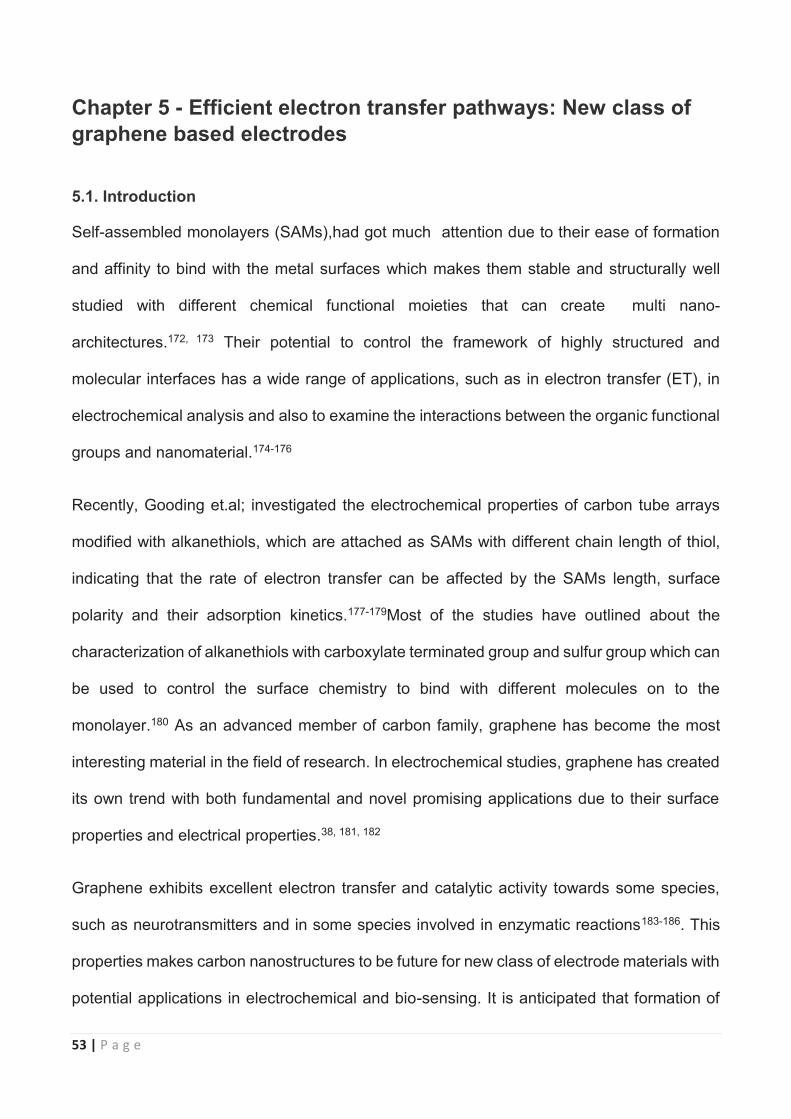
53 | P a g e
Chapter 5 - Efficient electron transfer pathways: New class of graphene based electrodes
5.1. Introduction
Self-assembled monolayers (SAMs),had got much attention due to their ease of formation
and affinity to bind with the metal surfaces which makes them stable and structurally well
studied with different chemical functional moieties that can create multi nano-
architectures.172, 173 Their potential to control the framework of highly structured and
molecular interfaces has a wide range of applications, such as in electron transfer (ET), in
electrochemical analysis and also to examine the interactions between the organic functional
groups and nanomaterial.174-176
Recently, Gooding et.al; investigated the electrochemical properties of carbon tube arrays
modified with alkanethiols, which are attached as SAMs with different chain length of thiol,
indicating that the rate of electron transfer can be affected by the SAMs length, surface
polarity and their adsorption kinetics.177-179Most of the studies have outlined about the
characterization of alkanethiols with carboxylate terminated group and sulfur group which can
be used to control the surface chemistry to bind with different molecules on to the
monolayer.180 As an advanced member of carbon family, graphene has become the most
interesting material in the field of research. In electrochemical studies, graphene has created
its own trend with both fundamental and novel promising applications due to their surface
properties and electrical properties.38, 181, 182
Graphene exhibits excellent electron transfer and catalytic activity towards some species,
such as neurotransmitters and in some species involved in enzymatic reactions183-186. This
properties makes carbon nanostructures to be future for new class of electrode materials with
potential applications in electrochemical and bio-sensing. It is anticipated that formation of
54 | P a g e
new class of graphene-SAM nanostructure and taking the benefits of the significant
properties of graphene and SAM, and further studying the hybrid material for advanced
electrochemical studies could give raise to a new field of research185, 187.
In this study, we report for very first time a new class of graphene electrode with different
CRGO’s sheet immobilized on CH3 and COOH terminated alkanethiol-modified Au electrodes
shown in the figure 30. Our main aim, is to reveal the minor changes in the electron transfer
(ET) after binding with CRGO’s on to the thiol, since the removal of oxygen functional groups
from the surface of graphene during theirincreased reduction time makes their surface more
hydrophobic and conductive.
Figure 30Schematic representation of CRGO’s self-assembly process on to the gold electrode (Mahesh, Power Point).
In most cases, SAM’s form into a very dense and firm film with long carbon chain length which
can block the electron transfer (ET) between the Au electrode surface and redox couple.40
ET can be restored after the attachment of nanomaterial on to the SAM’s either covalently or
non-covalently.32, 33, 41, 177, 188, 189
Our, present approach provides a step by step alteration in the electron transfer after the
fabrication of different CRGO’s with different reduction time on to the monolayer which
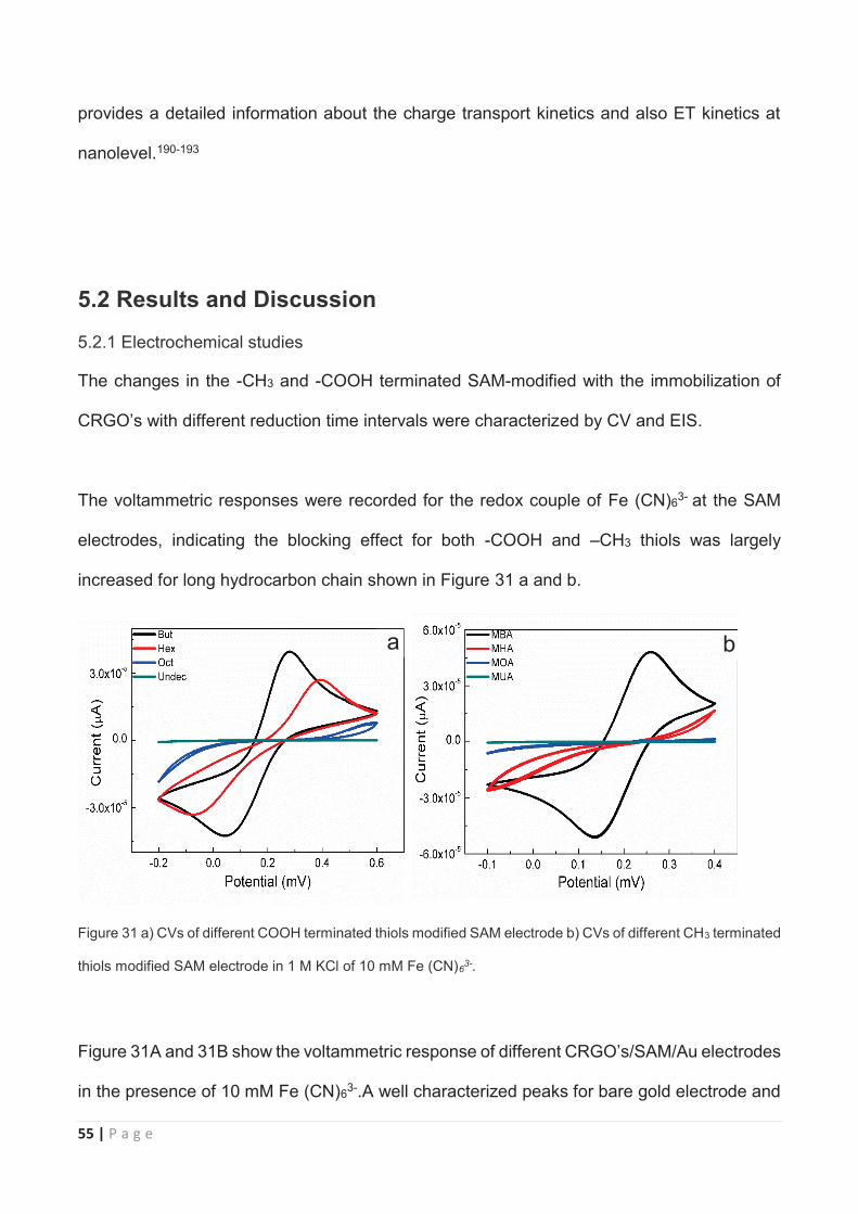
55 | P a g e
provides a detailed information about the charge transport kinetics and also ET kinetics at
nanolevel.190-193
5.2 Results and Discussion
5.2.1 Electrochemical studies
The changes in the -CH3 and -COOH terminated SAM-modified with the immobilization of
CRGO’s with different reduction time intervals were characterized by CV and EIS.
The voltammetric responses were recorded for the redox couple of Fe (CN)63- at the SAM
electrodes, indicating the blocking effect for both -COOH and –CH3 thiols was largely
increased for long hydrocarbon chain shown in Figure 31 a and b.
Figure 31 a) CVs of different COOH terminated thiols modified SAM electrode b) CVs of different CH3 terminated
thiols modified SAM electrode in 1 M KCl of 10 mM Fe (CN)63-.
Figure 31A and 31B show the voltammetric response of different CRGO’s/SAM/Au electrodes
in the presence of 10 mM Fe (CN)63-.A well characterized peaks for bare gold electrode and
a b

56 | P a g e
different -COOHterminated and -CH3 terminated self-assemblies on the gold electrode with
different peaks were observed, indicating the reaction between electrode and the redox
couple in the solution.
Figure 32A and 32B shows CV after the adsorption of CRGO’s with different reduction times
on the surface of different COOH terminated SAM’s such as MBA, MHA, MOA and MUA and
CH3 terminated SAM’s such as butanethiol, hexanethiol, octanethiol and undecanethiol
showed a change in ET behavior with a peak separation. It was observed that the adsorption
of CRGO’s with different reduction time showed a significant effect on the electrochemical
behavior of the CRGO/SAM/Au electrode. Withchange in the reduction time of CRGO’s a
change in the current-potential relationship was observed upon deposition of CRGO’s on
SAM. This is due to the restoration of heterogeneous ET on the CRGO’s/SAM/Au electrode
which is uniform with the nanomaterials (covalently33, 188, 194 and non-covalently195, 196) on the
gold electrode. Gooding’s177 group reported the restoration of ET by the attachment of metal
nanoparticles on the SAM by electrostatic interactions, which was due to the electron transfer
process.
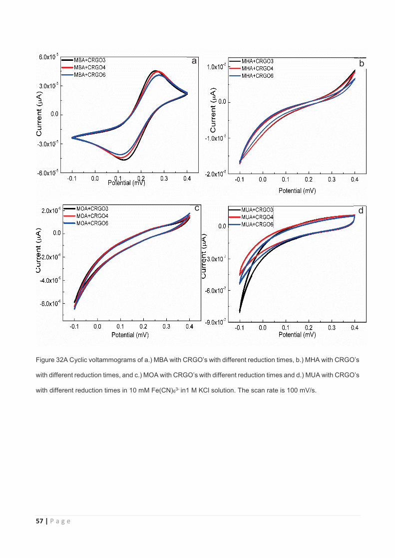
57 | P a g e
Figure 32A Cyclic voltammograms of a.) MBA with CRGO’s with different reduction times, b.) MHA with CRGO’s
with different reduction times, and c.) MOA with CRGO’s with different reduction times and d.) MUA with CRGO’s
with different reduction times in 10 mM Fe(CN)63- in1 M KCl solution. The scan rate is 100 mV/s.
a b
c d
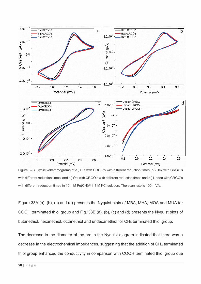
58 | P a g e
Figure 32B Cyclic voltammograms of a.) But with CRGO’s with different reduction times, b.) Hex with CRGO’s
with different reduction times, and c.) Oct with CRGO’s with different reduction times and d.) Undec with CRGO’s
with different reduction times in 10 mM Fe(CN)63- in1 M KCl solution. The scan rate is 100 mV/s.
Figure 33A (a), (b), (c) and (d) presents the Nyquist plots of MBA, MHA, MOA and MUA for
COOH terminated thiol group and Fig. 33B (a), (b), (c) and (d) presents the Nyquist plots of
butanethiol, hexanethiol, octanethiol and undecanethiol for CH3 terminated thiol group.
The decrease in the diameter of the arc in the Nyquist diagram indicated that there was a
decrease in the electrochemical impedances, suggesting that the addition of CH3 terminated
thiol group enhanced the conductivity in comparison with COOH terminated thiol group due
a b
c d
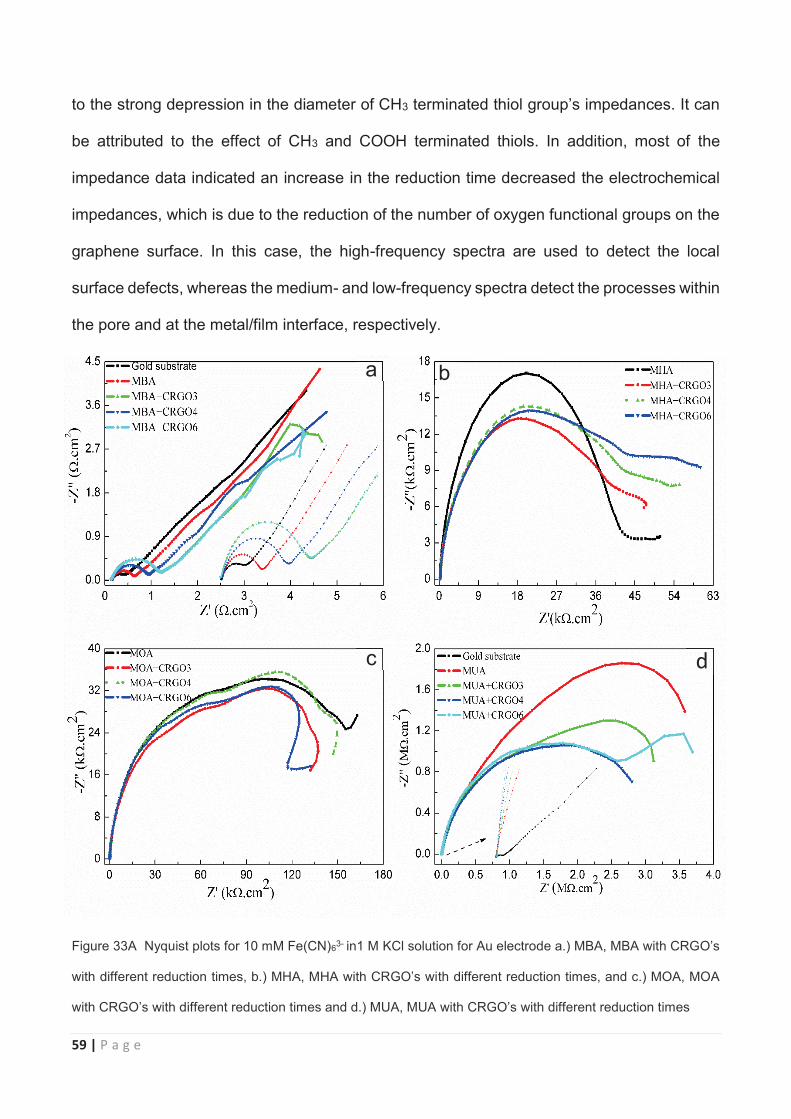
59 | P a g e
to the strong depression in the diameter of CH3 terminated thiol group’s impedances. It can
be attributed to the effect of CH3 and COOH terminated thiols. In addition, most of the
impedance data indicated an increase in the reduction time decreased the electrochemical
impedances, which is due to the reduction of the number of oxygen functional groups on the
graphene surface. In this case, the high-frequency spectra are used to detect the local
surface defects, whereas the medium- and low-frequency spectra detect the processes within
the pore and at the metal/film interface, respectively.
Figure 33A Nyquist plots for 10 mM Fe(CN)63- in1 M KCl solution for Au electrode a.) MBA, MBA with CRGO’s
with different reduction times, b.) MHA, MHA with CRGO’s with different reduction times, and c.) MOA, MOA
with CRGO’s with different reduction times and d.) MUA, MUA with CRGO’s with different reduction times
a b
c d
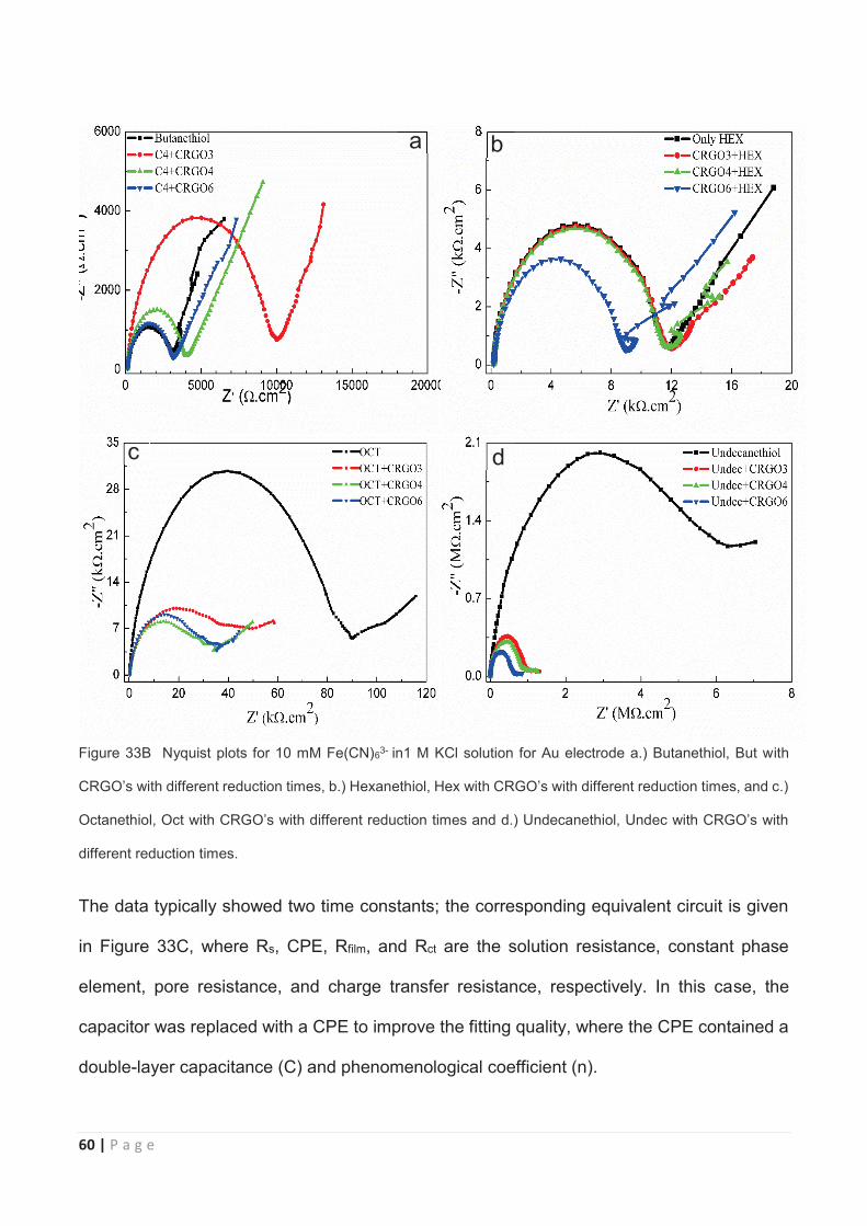
60 | P a g e
Figure 33B Nyquist plots for 10 mM Fe(CN)63- in1 M KCl solution for Au electrode a.) Butanethiol, But with
CRGO’s with different reduction times, b.) Hexanethiol, Hex with CRGO’s with different reduction times, and c.)
Octanethiol, Oct with CRGO’s with different reduction times and d.) Undecanethiol, Undec with CRGO’s with
different reduction times.
The data typically showed two time constants; the corresponding equivalent circuit is given
in Figure 33C, where Rs, CPE, Rfilm, and Rct are the solution resistance, constant phase
element, pore resistance, and charge transfer resistance, respectively. In this case, the
capacitor was replaced with a CPE to improve the fitting quality, where the CPE contained a
double-layer capacitance (C) and phenomenological coefficient (n).
a b
c d
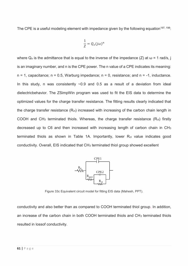
61 | P a g e
The CPE is a useful modeling element with impedance given by the following equation197, 198:
where Qo is the admittance that is equal to the inverse of the impedance (Z) at ω = 1 rad/s, j
is an imaginary number, and n is the CPE power. The n value of a CPE indicates its meaning:
n = 1, capacitance; n = 0.5, Warburg impedance; n = 0, resistance; and n = -1, inductance.
In this study, n was consistently ~0.9 and 0.5 as a result of a deviation from ideal
dielectricbehavior. The ZSimpWin program was used to fit the EIS data to determine the
optimized values for the charge transfer resistance. The fitting results clearly indicated that
the charge transfer resistance (Rct) increased with increasing of the carbon chain length in
COOH and CH3 terminated thiols. Whereas, the charge transfer resistance (Rct) firstly
decreased up to C6 and then increased with increasing length of carbon chain in CH3
terminated thiols as shown in Table 1A. Importantly, lower Rct value indicates good
conductivity. Overall, EIS indicated that CH3 terminated thiol group showed excellent
Figure 33c Equivalent circuit model for fitting EIS data (Mahesh, PPT).
conductivity and also better than as compared to COOH terminated thiol group. In addition,
an increase of the carbon chain in both COOH terminated thiols and CH3 terminated thiols
resulted in lossof conductivity.
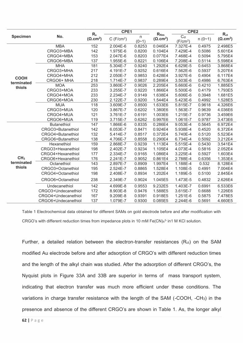
62 | P a g e
Specimen No. Rs (Ω.cm2)
CPE1 Rfilm (Ω.cm2)
CPE2 Rct (Ω.cm2) C (F/cm2) n
(0~1) Cdl
(F/cm2) n (0~1)
COOH terminated
thiols
MBA 152 2.004E-6 0.8253 0.046E4 7.327E-4 0.4975 2.498E5 CRGO3+MBA 142 1.975E-6 0.8200 0.104E4 7.429E-4 0.5086 5.601E4 CRGO4+MBA 153 2.047E-6 0.8203 0.077E4 7.468E-4 0.5094 5.795E4 CRGO6+MBA 137 1.955E-6 0.8221 0.106E4 7.208E-4 0.5114 5.598E4
MHA 181 5.304E-7 0.9240 1.292E4 6.629E-5 0.6453 3.868E4 CRGO3+MHA 217 4.191E-7 0.9252 0.616E4 7.562E-6 0.5937 5.207E4 CRGO4+MHA 212 2.050E-7 0.9853 0.428E4 3.927E-6 0.4904 6.117E4 CRGO6+ MHA 218 1.714E-7 0.9837 0.289E4 3.503E-6 0.4986 6.763E4
MOA 253 3.860E-7 0.9026 2.205E4 5.660E-6 0.4210 1.885E5 CRGO3+MOA 233 3.255E-7 0.9220 1.866E4 5.500E-6 0.4179 1.793E5 CRGO4+MOA 233 2.234E-7 0.9149 1.638E4 5.606E-6 0.3948 1.681E5 CRGO6+MOA 230 2.122E-7 0.9200 1.544E4 5.423E-6 0.4992 1.528E5
MUA 118 3.609E-7 0.8500 1.633E6 5.815E-7 0.9618 4.326E6 CRGO3+MUA 120 3.867E-7 0.6202 1.380E6 1.563E-7 0.9639 4.036E6 CRGO4+MUA 121 3.761E-7 0.6191 1.003E6 1.215E-7 0.9736 3.459E6 CRGO6+MUA 119 3.715E-7 0.6262 0.997E6 1.061E-7 0.9787 3.473E6
CH3 terminated
thiols
Butanethiol 147 1.866E-6 0.8335 0.286E4 9.053E-4 0.5645 6.972E4 CRGO3+Butanethiol 142 6.053E-7 0.8471 0.924E4 5.938E-4 0.4520 6.372E4 CRGO4+Butanethiol 132 5.414E-7 0.8517 0.372E4 5.740E-4 0.5120 5.523E4 CRGO6+Butanethiol 138 4.706E-7 0.8558 0.290E4 6.734E-4 0.5092 3.212E4
Hexanethiol 159 2.868E-7 0.9239 1.113E4 5.515E-4 0.5430 3.541E4 CRGO3+Hexanethiol 198 2.402E-7 0.9234 1.105E4 4.073E-4 0.5816 2.052E4 CRGO4+Hexanethiol 177 2.334E-7 0.9165 1.086E4 3.225E-4 0.5927 1.603E4 CRGO6+Hexanethiol 176 2.241E-7 0.9052 0.861E4 2.788E-4 0.6356 1.353E4
Octanethiol 143 2.897E-7 0.8909 1.997E4 1.188E-4 0.532 8.128E4 CRGO3+Octanethiol 195 2.524E-7 0.8865 1.528E4 1.108E-5 0.4991 7.004E4 CRGO4+Octanethiol 198 2.408E-7 0.8934 1.202E4 1.189E-5 0.5100 2.845E4 CRGO6+Octanethiol 238 2.349E-7 0.9024 1.045E5 1.473E-5 0.4832 2.626E4
Undecanethiol 142 4.699E-8 0.9553 9.232E5 1.403E-7 0.6991 6.533E6 CRGO3+Undecanethiol 172 8.903E-8 0.9476 1.588E5 3.615E-7 0.6688 1.226E6 CRGO4+Undecanethiol 167 9.209E-8 0.9391 0.918E5 1.251E-6 0.5875 7.478E5 CRGO6+Undecanethiol 137 1.079E-7 0.9300 0.085E5 2.244E-6 0.5691 4.660E5
Table 1 Electrochemical data obtained for different SAMs on gold electrode before and after modification with
CRGO’s with different reduction times from impedance plots in 10 mM Fe(CN)63- in1 M KCl solution.
Further, a detailed relation between the electron-transfer resistances (Rct) on the SAM
modified Au electrode before and after adsorption of CRGO’s with different reduction times
and the length of the alkyl chain was studied. After the adsorption of different CRGO’s, the
Nyquist plots in Figure 33A and 33B are superior in terms of mass transport system,
indicating that electron transfer was much more efficient under these conditions. The
variations in charge transfer resistance with the length of the SAM (-COOH, -CH3) in the
presence and absence of the different CRGO’s are shown in Table 1. As, the longer alkyl
63 | P a g e
thiols can form more densely closed packed structures than the shorter thiols which
resembles higher packing structures would guide to higher resistance when compared to
shorter ones. Till date most of the studies reported the influence of carbon chain length on
the packing thickness, intermolecular domain and geometry of self-assemblies.199, 200
The main aspect of this study, is to show that the charge transfer rate of the redox couple
can be calculated from Nyquist plot for the SAM modified Au electrode before and after
adsorption of CRGO’s with different reduction times. The charge transfer rate can be
calculated using following formula201:
Where kappis the apparent rate constant at the SAM-modified electrode, R is the gas constant,
T is temperature, F is the Faraday constant, the Rct is the charge transfer resistance and c is
the concentration of redox couple. The results are shown in the Table 1B.
The results in Table 1B clearly indicates the moderate change in the rate of charge transfer
between in each individual thiols before and after adsorption of CRGO’s. For electrode
terminated with SAM, the electrochemistry is blocked due to the presence of SAM. In case
of assemblies terminated with CRGO’s, the electrochemistry was well-defined and showed
an improved charge transfer (Rct). Figure 3A and 3B shows, with different CRGO’s, there is
a change in Rct. Therefore, the rate constant of electron transfer changes with different
CRGO’s. The results shows an additional proof to support the hypothesis that different
CRGO’s have the potential to act as “electron gate”, which forms a conducting pathways that
facilitate electron transfer through different CRGO’s if not blocked by SAMs. CRGO’s with
different reduction times influences the charge transfer rate after adsorption on to the SAM-
modified electrode. The observations clearly shows the rate of charge transfer varies with
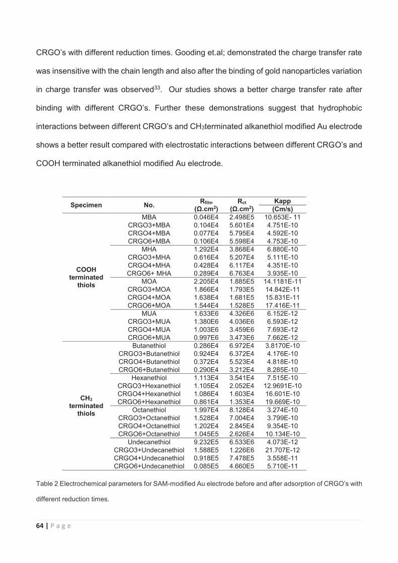
64 | P a g e
CRGO’s with different reduction times. Gooding et.al; demonstrated the charge transfer rate
was insensitive with the chain length and also after the binding of gold nanoparticles variation
in charge transfer was observed33. Our studies shows a better charge transfer rate after
binding with different CRGO’s. Further these demonstrations suggest that hydrophobic
interactions between different CRGO’s and CH3terminated alkanethiol modified Au electrode
shows a better result compared with electrostatic interactions between different CRGO’s and
COOH terminated alkanethiol modified Au electrode.
Table 2 Electrochemical parameters for SAM-modified Au electrode before and after adsorption of CRGO’s with
different reduction times.
Specimen No. Rfilm (Ω.cm2)
Rct (Ω.cm2)
Kapp (Cm/s)
COOH terminated
thiols
MBA 0.046E4 2.498E5 10.653E- 11 CRGO3+MBA 0.104E4 5.601E4 4.751E-10 CRGO4+MBA 0.077E4 5.795E4 4.592E-10 CRGO6+MBA 0.106E4 5.598E4 4.753E-10
MHA 1.292E4 3.868E4 6.880E-10 CRGO3+MHA 0.616E4 5.207E4 5.111E-10 CRGO4+MHA 0.428E4 6.117E4 4.351E-10 CRGO6+ MHA 0.289E4 6.763E4 3.935E-10
MOA 2.205E4 1.885E5 14.1181E-11 CRGO3+MOA 1.866E4 1.793E5 14.842E-11 CRGO4+MOA 1.638E4 1.681E5 15.831E-11 CRGO6+MOA 1.544E4 1.528E5 17.416E-11
MUA 1.633E6 4.326E6 6.152E-12 CRGO3+MUA 1.380E6 4.036E6 6.593E-12 CRGO4+MUA 1.003E6 3.459E6 7.693E-12 CRGO6+MUA 0.997E6 3.473E6 7.662E-12
CH3 terminated
thiols
Butanethiol 0.286E4 6.972E4 3.8170E-10 CRGO3+Butanethiol 0.924E4 6.372E4 4.176E-10 CRGO4+Butanethiol 0.372E4 5.523E4 4.818E-10 CRGO6+Butanethiol 0.290E4 3.212E4 8.285E-10
Hexanethiol 1.113E4 3.541E4 7.515E-10 CRGO3+Hexanethiol 1.105E4 2.052E4 12.9691E-10 CRGO4+Hexanethiol 1.086E4 1.603E4 16.601E-10 CRGO6+Hexanethiol 0.861E4 1.353E4 19.669E-10
Octanethiol 1.997E4 8.128E4 3.274E-10 CRGO3+Octanethiol 1.528E4 7.004E4 3.799E-10 CRGO4+Octanethiol 1.202E4 2.845E4 9.354E-10 CRGO6+Octanethiol 1.045E5 2.626E4 10.134E-10
Undecanethiol 9.232E5 6.533E6 4.073E-12 CRGO3+Undecanethiol 1.588E5 1.226E6 21.707E-12 CRGO4+Undecanethiol 0.918E5 7.478E5 3.558E-11 CRGO6+Undecanethiol 0.085E5 4.660E5 5.710E-11

65 | P a g e
5.3 Conclusion:
The electrochemical studies showed that the adsorption of CRGO’s with different reduction
times on to the electrode surface shows different electron transfer pathways which can
influence the electron transfer efficiency and also the rate of charge transfer. There is a strong
electrostatic interaction between COOH terminated SAM and CRGO’s and hydrophobic
interaction between CH3 terminated SAM and CRGO’s which shows a consistent effect on
the charge transfer resistance (Rct) and the apparent rate (kapp). The kinetics of ET activity
between the CRGO’s/SAM/Au electrode and redox species in the solution is attributed to
charge transfer being confined to CRGO’s with different reduction times. An increase of the
carbon chain in both COOH terminated thiols and CH3 terminated thiols lost the conductivity
due to long chain and high molecular weight which affects the conductivity. An increase in
the reduction time of graphene oxideslead to reduced number of oxygen functional groups
on their surface which significantly improves their conductivity.
66 | P a g e
Chapter 6 – Summary and future perspective
This chapter outlines the major findings in this project, which concludes the results of
graphene hybrid material and functionalised AuNPs self-assembly with graphene, which
opens a new route for the development of highly sensitive devices and actuators. On the
other hand, immobilization of different CRGO’s sheet on –COOH and –CH3 terminated
alkanethiols modified Au electrode showed an efficient electron transfer pathway which
paves path for new class of graphene electrode. This chapter also covers the future scope
from the current findings.
The assembly of graphene and its derivatives, which are cost-effective and easy to
synthesise, have made them favorable material for fabricating nanohybrids which could
be integrated with functionalised AuNPs and thiols. Fabrication of graphene hybrid
material have been done by sequential filtration of solution through vacuum filtration.
Incorporation of graphene into other materials has the promising advantage of improving
durability, mechanical strength, charge transport and other properties. In this thesis,
functionalised AuNPs sandwiched between graphene layers has been studied for
actuators and sensing applications.
6.1 A graphene hybrid Actuator
The graphene hybrid was successfully synthesised and the interactions were studied.
The binding of functionalised AuNPs and graphene is due to electrostatic interaction
between the positively charged functionalised AuNPs and negatively charged graphene
67 | P a g e
sheets. This graphene hybrid film showed good potential to be used as actuator for
artificial muscle application. The successful fabrication of graphene hybrid also improved
the stability of the device. Graphene hybrid actuator showed good movement with
application of different potentials and also, the charging and discharging of current
through the films in the process of deflection was observed by Anson plot. The
interactions between the functionalised AuNPs and graphene showed improvement in the
deflection, durability and life time of the device.
6.2 A highly sensitive pressure sensor based on graphene
hybrid
The graphene hybrid device was prepared by sequential filtration of solution through
vacuum filtration. To check the sensitivity of the device, good electronic and
electrochemical properties; surface uniformity and free standing film is preferred.
Moreover the device should be flexible and the fabrication process should be economical.
The addition of functionalised AuNPs to graphene showed tremendous improvement in
sensitivity and exhibits faster response with different weights. The hybrid device showed
a good response with minute forces, together with good response for tap and release
applications for real time monitoring devices. Further, the graphene hybrid can be used
as highly sensitive sensor for robotics and medical applications.
68 | P a g e
6.3 A new class of graphene electrode
The self-assembly of different CRGO’s onto the –COOH, -CH3 modified Au electrode
opens a new route in the development of new class of graphene electrodes for sensing
applications. Adetailed study of alkanethiols with two different end groups and their effect
on the Au electrode and type of interactions between different CRGO’s were taken into
consideration. The modification of SAM modified Au electrode with different CRGO’s in a
controlled manner is shown in chapter 5. Sufficient time had to be given to bind different
CRGO’s onto the SAM modified Au electrode. We clearly demonstrated the blocking
effect on the SAM modified Au electrode in the presence and absence of different
CRGO’s. The charge transfer resistance was found to be insensitive to the length of the
SAM. This new class of graphene electrodes showed significant changes in the rate of
charge transfer for different CRGO’s. Finally, CH3 terminated alkanethiol modified Au
electrode with different CRGO’s showed efficient charge transfer rate compared to COOH
terminated alkanethiols.
6.4 Future Perspective
The graphene hybrid materials has wide range of applications and definitely play an
important role in the future development of advanced hybrid materials for touch sensor,
actuators, energy storage and biosensor applications. Binding of graphene with other
materials helps to improve the conductivity, charge transport mechanism and mechanical
strength. Incorporation of one material into different functionalised materials can be useful
in obtaining new properties. A new method of approach for fabrication has been
developed for the construction of hybrid materials. Still particular efforts are required to

69 | P a g e
design and develop methods for the self-assembling hybrid nanostructures rather than
random mixing, which will drive a constant demand for optimized hybrid properties.
Future research on functionalised AuNPs sandwiched between graphene layers can be
helpful to improve performance and conductivity, which should be tested with different
applications. Investigation on the efficient electron transfer of different CRGO’s self-
assembled on –COOH, -CH3 modified Au electrode need to be carried out to further
investigate the step by step change in electron transfer with different CRGO’s. These
hybrid materials have the potential to for a wide range of applications such as sensors,
energy storage, touch screens, catalysis and photovoltaics.
70 | P a g e
7 References 1. Schulenburg, M.; Allemagne, R., Nanotechnology: Innovation for Tomorrow's World. EUR-OP: 2007. 2. Singh, V.; Joung, D.; Zhai, L.; Das, S.; Khondaker, S. I.; Seal, S. Progress in Materials Science 2011, 56, (8), 1178-1271. 3. Li, H.; He, X.; Kang, Z.; Huang, H.; Liu, Y.; Liu, J.; Lian, S.; Tsang, C. H. A.; Yang, X.; Lee, S. T. Angewandte Chemie International Edition 2010, 49, (26), 4430-4434. 4. Chen, H.; Müller, M. B.; Gilmore, K. J.; Wallace, G. G.; Li, D. Adv. Mater 2008, 20, (18), 3557-3561. 5. Shan, C.; Yang, H.; Han, D.; Zhang, Q.; Ivaska, A.; Niu, L. Biosensors and Bioelectronics 2010, 25, (5), 1070-1074. 6. Fan, Z.; Yan, J.; Zhi, L.; Zhang, Q.; Wei, T.; Feng, J.; Zhang, M.; Qian, W.; Wei, F. Advanced Materials 2010, 22, (33), 3723-3728. 7. Li, G. L.; Liu, G.; Li, M.; Wan, D.; Neoh, K.; Kang, E. The Journal of Physical Chemistry C 2010, 114, (29), 12742-12748. 8. Edwards, R. S.; Coleman, K. S. Nanoscale 2013, 5, (1), 38-51. 9. Vilatela, J. J.; Eder, D. ChemSusChem 2012, 5, (3), 456-478. 10. Eder, D. Chemical reviews 2010, 110, (3), 1348-1385. 11. Gómez-Romero, P.; Sanchez, C. New journal of chemistry 2005, 29, (1), 57-58. 12. Schottner, G. Chemistry of Materials 2001, 13, (10), 3422-3435. 13. Wu, Z.-S.; Ren, W.; Wen, L.; Gao, L.; Zhao, J.; Chen, Z.; Zhou, G.; Li, F.; Cheng, H.-M. ACS nano 2010, 4, (6), 3187-3194. 14. Baur, J.; Silverman, E. MRS bulletin 2007, 32, (04), 328-334. 15. Liao, S.-H.; Liu, P.-L.; Hsiao, M.-C.; Teng, C.-C.; Wang, C.-A.; Ger, M.-D.; Chiang, C.-L. Industrial & Engineering Chemistry Research 2012, 51, (12), 4573-4581. 16. Shearer, C. J.; Cherevan, A.; Eder, D. Advanced Materials 2014, 26, (15), 2295-2318. 17. Geim, A. K.; Novoselov, K. S. Nature materials 2007, 6, (3), 183-191. 18. Partoens, B.; Peeters, F. Physical Review B 2006, 74, (7), 075404. 19. Berger, C.; Song, Z.; Li, X.; Wu, X.; Brown, N.; Naud, C.; Mayou, D.; Li, T.; Hass, J.; Marchenkov, A. N. Science 2006, 312, (5777), 1191-1196. 20. Novoselov, K. S.; Geim, A. K.; Morozov, S.; Jiang, D.; Zhang, Y.; Dubonos, S. a.; Grigorieva, I.; Firsov, A. science 2004, 306, (5696), 666-669. 21. Krishnan, A.; Dujardin, E.; Treacy, M.; Hugdahl, J.; Lynum, S.; Ebbesen, T. Nature 1997, 388, (6641), 451-454. 22. Land, T.; Michely, T.; Behm, R.; Hemminger, J.; Comsa, G. Surface Science 1992, 264, (3), 261-270. 23. Nagashima, A.; Nuka, K.; Itoh, H.; Ichinokawa, T.; Oshima, C.; Otani, S. Surface Science 1993, 291, (1), 93-98. 24. Berger, C.; Song, Z.; Li, T.; Li, X.; Ogbazghi, A. Y.; Feng, R.; Dai, Z.; Marchenkov, A. N.; Conrad, E. H.; First, P. N. The Journal of Physical Chemistry B 2004, 108, (52), 19912-19916. 25. Coleman, J. N.; Lotya, M.; O’Neill, A.; Bergin, S. D.; King, P. J.; Khan, U.; Young, K.; Gaucher, A.; De, S.; Smith, R. J. Science 2011, 331, (6017), 568-571. 26. Yang, X.; Makita, Y.; Liu, Z.-h.; Ooi, K. Chemistry of materials 2003, 15, (6), 1228-1231. 27. Bao, J.; Fu, Y.; Bao, Z. Nanoscale research letters 2013, 8, (1), 1-6. 28. Chandra, V.; Park, J.; Chun, Y.; Lee, J. W.; Hwang, I.-C.; Kim, K. S. ACS nano 2010, 4, (7), 3979-3986. 29. Yavuz, C. T.; Mayo, J.; William, W. Y.; Prakash, A.; Falkner, J. C.; Yean, S.; Cong, L.; Shipley, H. J.; Kan, A.; Tomson, M. Science 2006, 314, (5801), 964-967. 30. Dreyer, D. R.; Park, S.; Bielawski, C. W.; Ruoff, R. S. Chemical Society Reviews 2010, 39, (1), 228-240.
71 | P a g e
31. Wang, X.; Tabakman, S. M.; Dai, H. Journal of the American Chemical Society 2008, 130, (26), 8152-8153. 32. Xie, X.; Zhao, K.; Xu, X.; Zhao, W.; Liu, S.; Zhu, Z.; Li, M.; Shi, Z.; Shao, Y. The Journal of Physical Chemistry C 2010, 114, (33), 14243-14250. 33. Shein, J. B.; Lai, L. M.; Eggers, P. K.; Paddon-Row, M. N.; Gooding, J. J. Langmuir 2009, 25, (18), 11121-11128. 34. Patolsky, F.; Lichtenstein, A.; Willner, I. Nature Biotechnology 2001, 19, (3), 253-257. 35. Xiao, Y.; Lubin, A. A.; Baker, B. R.; Plaxco, K. W.; Heeger, A. J. Proceedings of the National Academy of Sciences 2006, 103, (45), 16677-16680. 36. Zoski, C. G.; Simjee, N.; Guenat, O.; Koudelka-Hep, M. Analytical Chemistry 2004, 76, (1), 62-72. 37. Bond, A. M. Analyst 1994, 119, (11), 1R-21R. 38. Li, D.; Kaner, R. B. Nat Nanotechnol 2008, 3, 101. 39. Allen, M. J.; Tung, V. C.; Kaner, R. B. Chemical reviews 2009, 110, (1), 132-145. 40. Zhang, B.; Fan, L.; Zhong, H.; Liu, Y.; Chen, S. Journal of the American Chemical Society 2013, 135, (27), 10073-10080. 41. Yang, S.; Xu, B.; Zhang, J.; Huang, X.; Ye, J.; Yu, C. The Journal of Physical Chemistry C 2010, 114, (10), 4389-4393. 42. Huang, Y.; Liang, J.; Chen, Y. Journal of Materials Chemistry 2012, 22, (9), 3671-3679. 43. Liang, J.; Huang, Y.; Oh, J.; Kozlov, M.; Sui, D.; Fang, S.; Baughman, R. H.; Ma, Y.; Chen, Y. Advanced Functional Materials 2011, 21, (19), 3778-3784. 44. Park, S.; An, J.; Suk, J. W.; Ruoff, R. S. Small 2010, 6, (2), 210-212. 45. Raguse, B.; Müller, K. H.; Wieczorek, L. Advanced Materials 2003, 15, (11), 922-926. 46. Tegin, J.; Wikander, J. Industrial Robot: An International Journal 2005, 32, (1), 64-70. 47. Sokhanvar, S.; Packirisamy, M.; Dargahi, J. Smart materials and structures 2007, 16, (4), 989. 48. Teng, X.-F.; Zhang, Y.-T.; Poon, C. C.; Bonato, P. Biomedical Engineering, IEEE Reviews in 2008, 1, 62-74. 49. Farcau, C.; Moreira, H.; Viallet, B.; Grisolia, J.; Ciuculescu-Pradines, D.; Amiens, C.; Ressier, L. The Journal of Physical Chemistry C 2011, 115, (30), 14494-14499. 50. Tang, J.; Skotadis, E.; Stathopoulos, S.; Roussi, V.; Tsouti, V.; Tsoukalas, D. Sensors and Actuators B: Chemical 2012, 170, 129-136. 51. Segev-Bar, M.; Haick, H. ACS nano 2013, 7, (10), 8366-8378. 52. Herrmann, J.; Müller, K.-H.; Reda, T.; Baxter, G. R.; Raguse, B.; de Groot, G. J. J. B.; Chai, R.; Roberts, M.; Wieczorek, L. Applied Physics Letters 2007, 91, (18), -. 53. Chen, D.; Zhang, H.; Liu, Y.; Li, J. Energy & Environmental Science 2013, 6, (5), 1362-1387. 54. Wang, Y.; Shao, Y.; Matson, D. W.; Li, J.; Lin, Y. ACS nano 2010, 4, (4), 1790-1798. 55. Fan, Y.; Zhao, M.; Wang, Z.; Zhang, X.; Zhang, H. Applied Physics Letters 2011, 98, (8), 083103. 56. Lin, Y.-M.; Avouris, P. Nano letters 2008, 8, (8), 2119-2125. 57. Barone, V.; Hod, O.; Scuseria, G. E. Nano letters 2006, 6, (12), 2748-2754. 58. Jayasekera, T.; Mintmire, J. Nanotechnology 2007, 18, (42), 424033. 59. Wang, X.; Ouyang, Y.; Li, X.; Wang, H.; Guo, J.; Dai, H. Physical review letters 2008, 100, (20), 206803. 60. Kim, S.; Nah, J.; Jo, I.; Shahrjerdi, D.; Colombo, L.; Yao, Z.; Tutuc, E.; Banerjee, S. K. arXiv preprint arXiv:0901.2901 2009. 61. Ou, T.-M.; Borsa, T.; Van Zeghbroeck, B. In Graphene junction field-effect transistor, APS Meeting Abstracts, 2014; p 48011. 62. Britnell, L.; Gorbachev, R.; Jalil, R.; Belle, B.; Schedin, F.; Mishchenko, A.; Georgiou, T.; Katsnelson, M.; Eaves, L.; Morozov, S. Science 2012, 335, (6071), 947-950.
72 | P a g e
63. Meric, I.; Han, M. Y.; Young, A. F.; Ozyilmaz, B.; Kim, P.; Shepard, K. L. Nature nanotechnology 2008, 3, (11), 654-659. 64. Obradovic, B.; Kotlyar, R.; Heinz, F.; Matagne, P.; Rakshit, T.; Giles, M.; Stettler, M.; Nikonov, D. Applied Physics Letters 2006, 88, (14), 142102. 65. Mohamadpour, H.; Asgari, A. Physica E: Low-dimensional Systems and Nanostructures 2012, 46, 270-273. 66. Xia, F.; Farmer, D. B.; Lin, Y.-m.; Avouris, P. Nano letters 2010, 10, (2), 715-718. 67. Lu, C.-C.; Lin, Y.-C.; Yeh, C.-H.; Huang, J.-C.; Chiu, P.-W. ACS nano 2012, 6, (5), 4469-4474. 68. Szafranek, B. N.; Schall, D.; Otto, M.; Neumaier, D.; Kurz, H. Nano letters 2011, 11, (7), 2640-2643. 69. Echtermeyer, T. J.; Lemme, M. C.; Baus, M.; Szafranek, B. N.; Geim, A. K.; Kurz, H. Electron Device Letters, IEEE 2008, 29, (8), 952-954. 70. Szafranek, B.; Fiori, G.; Schall, D.; Neumaier, D.; Kurz, H. Nano letters 2012, 12, (3), 1324-1328. 71. Gwon, H.; Kim, H.-S.; Lee, K. U.; Seo, D.-H.; Park, Y. C.; Lee, Y.-S.; Ahn, B. T.; Kang, K. Energy & Environmental Science 2011, 4, (4), 1277-1283. 72. Pumera, M. Energy & Environmental Science 2011, 4, (3), 668-674. 73. Li, B.; Cao, H.; Shao, J.; Qu, M.; Warner, J. H. Journal of Materials Chemistry 2011, 21, (13), 5069-5075. 74. Arico, A. S.; Bruce, P.; Scrosati, B.; Tarascon, J.-M.; Van Schalkwijk, W. Nature materials 2005, 4, (5), 366-377. 75. Feckl, J. M.; Fominykh, K.; Döblinger, M.; Fattakhova-Rohlfing, D.; Bein, T. Angewandte Chemie International Edition 2012, 51, (30), 7459-7463. 76. Wang, H.; Cui, L.-F.; Yang, Y.; Sanchez Casalongue, H.; Robinson, J. T.; Liang, Y.; Cui, Y.; Dai, H. Journal of the American Chemical Society 2010, 132, (40), 13978-13980. 77. Zhu, N.; Liu, W.; Xue, M.; Xie, Z.; Zhao, D.; Zhang, M.; Chen, J.; Cao, T. Electrochimica Acta 2010, 55, (20), 5813-5818. 78. Li, Y.; Wang, H.; Xie, L.; Liang, Y.; Hong, G.; Dai, H. Journal of the American Chemical Society 2011, 133, (19), 7296-7299. 79. Xiao, J.; Mei, D.; Li, X.; Xu, W.; Wang, D.; Graff, G. L.; Bennett, W. D.; Nie, Z.; Saraf, L. V.; Aksay, I. A. Nano letters 2011, 11, (11), 5071-5078. 80. Wang, L.; Wang, H.; Liu, Z.; Xiao, C.; Dong, S.; Han, P.; Zhang, Z.; Zhang, X.; Bi, C.; Cui, G. Solid State Ionics 2010, 181, (37), 1685-1689. 81. Tang, Z.; Tang, C. h.; Gong, H. Advanced Functional Materials 2012, 22, (6), 1272-1278. 82. Cheng, Q.; Tang, J.; Ma, J.; Zhang, H.; Shinya, N.; Qin, L.-C. Physical Chemistry Chemical Physics 2011, 13, (39), 17615-17624. 83. Kim, H.; Abdala, A. A.; Macosko, C. W. Macromolecules 2010, 43, (16), 6515-6530. 84. Yang, W.; Chen, G.; Shi, Z.; Liu, C.-C.; Zhang, L.; Xie, G.; Cheng, M.; Wang, D.; Yang, R.; Shi, D. Nature materials 2013, 12, (9), 792-797. 85. Wang, Y.; Shi, Z.; Huang, Y.; Ma, Y.; Wang, C.; Chen, M.; Chen, Y. The Journal of Physical Chemistry C 2009, 113, (30), 13103-13107. 86. Mao, S.; Lu, G.; Yu, K.; Bo, Z.; Chen, J. Advanced materials 2010, 22, (32), 3521-3526. 87. Luo, X.; Morrin, A.; Killard, A. J.; Smyth, M. R. Electroanalysis 2006, 18, (4), 319-326. 88. Fiorito, P. A.; Gonçales, V. R.; Ponzio, E. A.; de Torresi, S. I. C. Chemical Communications 2005, (3), 366-368. 89. Xu, J.-J.; Zhao, W.; Luo, X.-L.; Chen, H.-Y. Chemical Communications 2005, (6), 792-794. 90. Xiao, Y.; Patolsky, F.; Katz, E.; Hainfeld, J. F.; Willner, I. Science 2003, 299, (5614), 1877-1881. 91. Selvin, P. R. Nature structural biology 2000, 7, (9), 730-734. 92. Lu, L.-M.; Li, H.-B.; Qu, F.; Zhang, X.-B.; Shen, G.-L.; Yu, R.-Q. Biosensors and Bioelectronics 2011, 26, (8), 3500-3504.
73 | P a g e
93. Jang, H. D.; Kim, S. K.; Chang, H.; Roh, K.-M.; Choi, J.-W.; Huang, J. Biosensors and Bioelectronics 2012, 38, (1), 184-188. 94. Kodali, V. K.; Scrimgeour, J.; Kim, S.; Hankinson, J. H.; Carroll, K. M.; De Heer, W. A.; Berger, C.; Curtis, J. E. Langmuir 2010, 27, (3), 863-865. 95. Zhang, N.; Li, R.; Zhang, L.; Chen, H.; Wang, W.; Liu, Y.; Wu, T.; Wang, X.; Wang, W.; Li, Y. Soft Matter 2011, 7, (16), 7231-7239. 96. Yang, W.; Ratinac, K. R.; Ringer, S. P.; Thordarson, P.; Gooding, J. J.; Braet, F. Angewandte Chemie International Edition 2010, 49, (12), 2114-2138. 97. Feng, L.; Liu, Z. Nanomedicine 2011, 6, (2), 317-324. 98. Lian, W.; Liu, S.; Yu, J.; Xing, X.; Li, J.; Cui, M.; Huang, J. Biosensors and Bioelectronics 2012, 38, (1), 163-169. 99. Shen, H.; Zhang, L.; Liu, M.; Zhang, Z. Theranostics 2012, 2, (3), 283. 100. McCormick, F. Nature Reviews Cancer 2001, 1, (2), 130-141. 101. Zhang, Y.; Nayak, T. R.; Hong, H.; Cai, W. Nanoscale 2012, 4, (13), 3833-3842. 102. Liu, C.; Zhang, P.; Zhai, X.; Tian, F.; Li, W.; Yang, J.; Liu, Y.; Wang, H.; Wang, W.; Liu, W. Biomaterials 2012, 33, (13), 3604-3613. 103. Kim, H.; Namgung, R.; Singha, K.; Oh, I.-K.; Kim, W. J. Bioconjugate chemistry 2011, 22, (12), 2558-2567. 104. Bao, H.; Pan, Y.; Ping, Y.; Sahoo, N. G.; Wu, T.; Li, L.; Li, J.; Gan, L. H. Small 2011, 7, (11), 1569-1578. 105. Sundar, S.; Prajapati, V. K. Current medicinal chemistry 2012, 19, (19), 3196. 106. Wen, H.; Dong, C.; Dong, H.; Shen, A.; Xia, W.; Cai, X.; Song, Y.; Li, X.; Li, Y.; Shi, D. Small 2012, 8, (5), 760-769. 107. Piochon, C.; Kloth, A. D.; Grasselli, G.; Titley, H. K.; Nakayama, H.; Hashimoto, K.; Wan, V.; Simmons, D. H.; Eissa, T.; Nakatani, J. Nature communications 2014, 5. 108. Rana, V. K.; Choi, M. C.; Kong, J. Y.; Kim, G. Y.; Kim, M. J.; Kim, S. H.; Mishra, S.; Singh, R. P.; Ha, C. S. Macromolecular Materials and Engineering 2011, 296, (2), 131-140. 109. Goenka, S.; Sant, V.; Sant, S. Journal of Controlled Release 2014, 173, 75-88. 110. Ryoo, S.-R.; Kim, Y.-K.; Kim, M.-H.; Min, D.-H. Acs Nano 2010, 4, (11), 6587-6598. 111. Yang, K.; Wan, J.; Zhang, S.; Tian, B.; Zhang, Y.; Liu, Z. Biomaterials 2012, 33, (7), 2206-2214. 112. Fiorillo, M.; Verre, A. F.; Iliut, M.; Peiris-Pagés, M.; Ozsvari, B.; Gandara, R.; Cappello, A. R.; Sotgia, F.; Vijayaraghavan, A.; Lisanti, M. P. Oncotarget 2015, 6, (6), 3553. 113. Zhou, Y.; Bao, Q.; Tang, L. A. L.; Zhong, Y.; Loh, K. P. Chemistry of Materials 2009, 21, (13), 2950-2956. 114. Tian, B.; Wang, C.; Zhang, S.; Feng, L.; Liu, Z. ACS nano 2011, 5, (9), 7000-7009. 115. Weng, Z.; Wang, H.; Vongsvivut, J.; Li, R.; Glushenkov, A. M.; He, J.; Chen, Y.; Barrow, C. J.; Yang, W. Analytica chimica acta 2013, 803, 128-134. 116. Baughman, R. H.; Cui, C.; Zakhidov, A. A.; Iqbal, Z.; Barisci, J. N.; Spinks, G. M.; Wallace, G. G.; Mazzoldi, A.; De Rossi, D.; Rinzler, A. G. Science 1999, 284, (5418), 1340-1344. 117. Jung, J.-H.; Jeon, J.-H.; Sridhar, V.; Oh, I.-K. Carbon 2011, 49, (4), 1279-1289. 118. Loomis, J.; King, B.; Burkhead, T.; Xu, P.; Bessler, N.; Terentjev, E.; Panchapakesan, B. Nanotechnology 2012, 23, (4), 045501. 119. Fusco, S.; Sakar, M. S.; Kennedy, S.; Peters, C.; Bottani, R.; Starsich, F.; Mao, A.; Sotiriou, G. A.; Pané, S.; Pratsinis, S. E. Advanced Materials 2014, 26, (6), 952-957. 120. Baker, C. O.; Shedd, B.; Innis, P. C.; Whitten, P. G.; Spinks, G. M.; Wallace, G. G.; Kaner, R. B. Advanced Materials 2008, 20, (1), 155-158. 121. de Lima, C. R.; Vatanabe, S. L.; Choi, A.; Nakasone, P. H.; Pires, R. F.; Silva, E. C. N. Sensors and Actuators A: Physical 2009, 152, (1), 110-118.
74 | P a g e
122. Kim, B.; Lee, S.; Park, J. H.; Park, J.-O. Mechatronics, IEEE/ASME Transactions on 2005, 10, (1), 77-86. 123. Liang, J.; Xu, Y.; Huang, Y.; Zhang, L.; Wang, Y.; Ma, Y.; Li, F.; Guo, T.; Chen, Y. The Journal of Physical Chemistry C 2009, 113, (22), 9921-9927. 124. Krishnamoorthy, G.; Tesar, D. In Multi-Sensor Architecture for Intelligent Electromechanical Actuators, Proceedings of the 12 th IFtoMM World Congress, 2007; Citeseer. 125. Yu, D.; Dai, L. The Journal of Physical Chemistry Letters 2009, 1, (2), 467-470. 126. Kong, L.; Chen, W. Advanced Materials 2014, 26, (7), 1025-1043. 127. Liang, J.; Huang, L.; Li, N.; Huang, Y.; Wu, Y.; Fang, S.; Oh, J.; Kozlov, M.; Ma, Y.; Li, F. ACS nano 2012, 6, (5), 4508-4519. 128. Bar-Cohen, Y. 2004. 129. Spinks, G. M.; Wallace, G. G.; Fifield, L. S.; Dalton, L. R.; Mazzoldi, A.; De Rossi, D.; Khayrullin, I. I.; Baughman, R. H. Advanced Materials 2002, 14, (23), 1728-1732. 130. Hughes, M.; Spinks, G. M. Advanced Materials 2005, 17, (4), 443-446. 131. Mirfakhrai, T.; Oh, J.; Kozlov, M.; Fang, S.; Zhang, M.; Baughman, R. H.; Madden, J. D. Journal of the Electrochemical Society 2009, 156, (6), K97-K103. 132. Landi, B. J.; Raffaelle, R. P.; Heben, M. J.; Alleman, J. L.; VanDerveer, W.; Gennett, T. Nano Letters 2002, 2, (11), 1329-1332. 133. Terasawa, N.; Ono, N.; Mukai, K.; Koga, T.; Higashi, N.; Asaka, K. Carbon 2012, 50, (1), 311-320. 134. Yun, Y.; Shanov, V.; Tu, Y.; Schulz, M. J.; Yarmolenko, S.; Neralla, S.; Sankar, J.; Subramaniam, S. Nano letters 2006, 6, (4), 689-693. 135. Kim, U.; Kang, J.; Lee, C.; Kwon, H. Y.; Hwang, S.; Moon, H.; Koo, J. C.; Nam, J.-D.; Hong, B. H.; Choi, J.-B. Nanotechnology 2013, 24, (14), 145501. 136. Zhao, Y.; Song, L.; Zhang, Z.; Qu, L. Energy & Environmental Science 2013, 6, (12), 3520-3536. 137. Zhu, S.-E.; Shabani, R.; Rho, J.; Kim, Y.; Hong, B. H.; Ahn, J.-H.; Cho, H. J. Nano letters 2011, 11, (3), 977-981. 138. Cao, J.; Wang, Y.; Zhou, Y.; Ouyang, J.-H.; Jia, D.; Guo, L. Journal of Electroanalytical Chemistry 2013, 689, 201-206. 139. Liu, K.; Zhang, J.-J.; Cheng, F.-F.; Zheng, T.-T.; Wang, C.; Zhu, J.-J. Journal of Materials Chemistry 2011, 21, (32), 12034-12040. 140. Storhoff, J. J.; Lazarides, A. A.; Mucic, R. C.; Mirkin, C. A.; Letsinger, R. L.; Schatz, G. C. Journal of the American Chemical Society 2000, 122, (19), 4640-4650. 141. Wang, H.; Hao, Q.; Yang, X.; Lu, L.; Wang, X. ACS applied materials & interfaces 2010, 2, (3), 821-828. 142. Li, D.; Mueller, M. B.; Gilje, S.; Kaner, R. B.; Wallace, G. G. Nature nanotechnology 2008, 3, (2), 101-105. 143. Xu, Y.; Zhao, L.; Bai, H.; Hong, W.; Li, C.; Shi, G. Journal of the American Chemical Society 2009, 131, (37), 13490-13497. 144. Yang, W.; Justin Gooding, J.; Brynn Hibbert, D. Journal of electroanalytical chemistry 2001, 516, (1), 10-16. 145. Li, Y.; Schluesener, H. J.; Xu, S. Gold Bulletin 2010, 43, (1), 29-41. 146. Han, G.; Ghosh, P.; Rotello, V. M. 2007. 147. Rosi, N. L.; Giljohann, D. A.; Thaxton, C. S.; Lytton-Jean, A. K.; Han, M. S.; Mirkin, C. A. Science 2006, 312, (5776), 1027-1030. 148. Qian, X.; Park, H. S. Nanotechnology 2010, 21, (36), 365704. 149. Yin, J.; Hu, P.; Luo, J.; Wang, L.; Cohen, M. F.; Zhong, C.-J. ACS nano 2011, 5, (8), 6516-6526. 150. Bhattacharya, S.; Srivastava, A. Langmuir 2003, 19, (10), 4439-4447. 151. Burkett, S. L.; Mann, S. Chem. Commun. 1996, (3), 321-322.
75 | P a g e
152. Daniel, M.-C.; Astruc, D. Chemical reviews 2004, 104, (1), 293-346. 153. Xu, C.; Wang, X.; Zhu, J. The Journal of Physical Chemistry C 2008, 112, (50), 19841-19845. 154. Hong, W.; Bai, H.; Xu, Y.; Yao, Z.; Gu, Z.; Shi, G. The Journal of Physical Chemistry C 2010, 114, (4), 1822-1826. 155. Shao, Y.; Wang, J.; Wu, H.; Liu, J.; Aksay, I. A.; Lin, Y. Electroanalysis 2010, 22, (10), 1027-1036. 156. Liu, Z.; Robinson, J. T.; Sun, X.; Dai, H. Journal of the American Chemical Society 2008, 130, (33), 10876-10877. 157. Xu, Y.; Liu, Z.; Zhang, X.; Wang, Y.; Tian, J.; Huang, Y.; Ma, Y.; Zhang, X.; Chen, Y. Advanced Materials 2009, 21, (12), 1275-1279. 158. Yang, H.; Shan, C.; Li, F.; Han, D.; Zhang, Q.; Niu, L. Chem. Commun. 2009, (26), 3880-3882. 159. Li, D.; Liu, J.; Barrow, C. J.; Yang, W. Chemical Communications 2014, 50, (60), 8197-8200. 160. Gong, S.; Schwalb, W.; Wang, Y.; Chen, Y.; Tang, Y.; Si, J.; Shirinzadeh, B.; Cheng, W. Nature communications 2014, 5. 161. Cote, L. J.; Kim, F.; Huang, J. Journal of the American Chemical Society 2008, 131, (3), 1043-1049. 162. Kim, J.; Cote, L. J.; Kim, F.; Huang, J. Journal of the American Chemical Society 2009, 132, (1), 260-267. 163. Tien, H.-W.; Huang, Y.-L.; Yang, S.-Y.; Wang, J.-Y.; Ma, C.-C. M. Carbon 2011, 49, (5), 1550-1560. 164. Berciaud, S.; Ryu, S.; Brus, L. E.; Heinz, T. F. Nano letters 2008, 9, (1), 346-352. 165. Kudin, K. N.; Ozbas, B.; Schniepp, H. C.; Prud'Homme, R. K.; Aksay, I. A.; Car, R. Nano letters 2008, 8, (1), 36-41. 166. Huang, I. Y.; Lee, M. C. Sensors and Actuators B: Chemical 2008, 132, (1), 340-348. 167. Yang, X.; Tu, Y.; Li, L.; Shang, S.; Tao, X.-m. ACS applied materials & interfaces 2010, 2, (6), 1707-1713. 168. Kumar, N. A.; Kim, S. H.; Kim, J. S.; Kim, J. T.; Jeong, Y. T. Surface Review and Letters 2009, 16, (03), 487-492. 169. Han, T. H.; Lee, W. J.; Lee, D. H.; Kim, J. E.; Choi, E. Y.; Kim, S. O. Advanced Materials 2010, 22, (18), 2060-2064. 170. Alvares, D.; Wieczorek, L.; Raguse, B.; Ladouceur, F.; Lovell, N. Procedia Engineering 2011, 25, 1349-1352. 171. Wang, X.; Gu, Y.; Xiong, Z.; Cui, Z.; Zhang, T. Advanced Materials 2014, 26, (9), 1336-1342. 172. Xing, Y.; O'Shea, S.; Li, S. Journal of Electroanalytical Chemistry 2003, 542, 7-11. 173. Gooding, J. J.; Mearns, F.; Yang, W.; Liu, J. Electroanalysis 2003, 15, (2), 81-96. 174. Wink, T.; Van Zuilen, S.; Bult, A.; Van Bennekom, W. Analyst 1997, 122, (4), 43R-50R. 175. Hu, X.; Dong, S. Journal of Materials Chemistry 2008, 18, (12), 1279-1295. 176. Lim, S. I.; Zhong, C.-J. Accounts of chemical research 2009, 42, (6), 798-808. 177. Chou, A.; Eggers, P. K.; Paddon-Row, M. N.; Gooding, J. J. The Journal of Physical Chemistry C 2009, 113, (8), 3203-3211. 178. Eggers, P. K.; Hibbert, D. B.; Paddon-Row, M. N.; Gooding, J. J. The Journal of Physical Chemistry C 2009, 113, (20), 8964-8971. 179. Subramanian, R.; Lakshminarayanan, V. Electrochimica Acta 2000, 45, (27), 4501-4509. 180. Mendes, R. K.; Freire, R. S.; Fonseca, C. P.; Neves, S.; Kubota, L. T. Journal of the Brazilian Chemical Society 2004, 15, (6), 849-855. 181. Wu, J.; Pisula, W.; Müllen, K. Chemical Reviews 2007, 107, (3), 718-747. 182. Brownson, D. A.; Kampouris, D. K.; Banks, C. E. Chemical Society Reviews 2012, 41, (21), 6944-6976. 183. Shang, N. G.; Papakonstantinou, P.; McMullan, M.; Chu, M.; Stamboulis, A.; Potenza, A.; Dhesi, S. S.; Marchetto, H. Advanced functional materials 2008, 18, (21), 3506-3514.
76 | P a g e
184. Alwarappan, S.; Erdem, A.; Liu, C.; Li, C.-Z. Journal of Physical Chemistry C 2009, 113, (20), 8853-8857. 185. Zhou, M.; Zhai, Y.; Dong, S. Analytical Chemistry 2009, 81, (14), 5603-5613. 186. Shan, C.; Yang, H.; Song, J.; Han, D.; Ivaska, A.; Niu, L. Analytical Chemistry 2009, 81, (6), 2378-2382. 187. Zhou, X.; Huang, X.; Qi, X.; Wu, S.; Xue, C.; Boey, F. Y.; Yan, Q.; Chen, P.; Zhang, H. The Journal of Physical Chemistry C 2009, 113, (25), 10842-10846. 188. Chen, Z.; Yang, Y.; Wu, Z.; Luo, G.; Xie, L.; Liu, Z.; Ma, S.; Guo, W. The Journal of Physical Chemistry B 2005, 109, (12), 5473-5477. 189. Bradbury, C. R.; Zhao, J.; Fermín, D. J. The Journal of Physical Chemistry C 2008, 112, (27), 10153-10160. 190. PENNER, R.; HEBEN, M.; LONGIN, T.; LEWIS, N. Science 1990, 250, (4984), 1118-1121. 191. Wang, Y.; Velmurugan, J.; Mirkin, M. V. Israel Journal of Chemistry 2010, 50, (3), 291-305. 192. Sun, P.; Mirkin, M. V. Analytical chemistry 2006, 78, (18), 6526-6534. 193. Chen, S.; Kucernak, A. The Journal of Physical Chemistry B 2002, 106, (36), 9396-9404. 194. Diao, P.; Liu, Z. The Journal of Physical Chemistry B 2005, 109, (44), 20906-20913. 195. Zhao, J.; Wasem, M.; Bradbury, C. R.; Fermín, D. J. The Journal of Physical Chemistry C 2008, 112, (18), 7284-7289. 196. Zhao, J.; Bradbury, C. R.; Fermín, D. J. The Journal of Physical Chemistry C 2008, 112, (17), 6832-6841. 197. McDonald, J. R. J. WILEY and Sons, New York 1987. 198. Nam, N. D.; Kim, M. J.; Kim, J. G. Metallurgical and Materials Transactions A 2014, 45, (2), 893-905. 199. Ulman, A. Chemical Reviews 1996, 96, (4), 1533-1554. 200. Ding, S.-J.; Chang, B.-W.; Wu, C.-C.; Lai, M.-F.; Chang, H.-C. Analytica chimica acta 2005, 554, (1), 43-51. 201. Bain, C. D.; Evall, J.; Whitesides, G. M. Journal of the American Chemical Society 1989, 111, (18), 7155-7164.

77 | P a g e
8 Appendices Gold (III) chloride trihydrate
Sigma Aldrich (AUS)
sodium citrate tribasic dehydrate Sigma Aldrich (AUS)
cystamine sulfate hydrate Sigma Aldrich (AUS)
Butanethiol Sigma Aldrich (AUS)
Hexanethiol Sigma Aldrich (AUS)
Octanethiol Sigma Aldrich (AUS)
Undecanethiol Sigma Aldrich (AUS)
Mercaptobenzoic acid Sigma Aldrich (AUS)
Mercaptohexanoic acid Sigma Aldrich (AUS)
Mercaptooctanoic acid Sigma Aldrich (AUS)

78 | P a g e
mercaptoundecanoic acid Sigma Aldrich (AUS)
Potassium ferricyanide Sigma Aldrich (AUS)
N,N-Dimethylformamide Sigma Aldrich (AUS)
Potassium Chloride Sigma Aldrich (AUS)