synergistic processor unit, instruction set architecturemidor/ese545/cell_spu_isa_v10.pdf ·...
TRANSCRIPT

Synergistic Processor Unit
Instruction Set Architecture
Version 1.0
August 1, 2005
Title Page

Copyright and Disclaimer© Copyright International Business Machines Corporation, Sony Computer Entertainment Incorporated, Toshiba Corporation 2005
All Rights ReservedPrinted in the United States of America August 2005
“ SONY ” and “*****“ are registered trademarks of Sony Corporation.
Other company, product, and service names may be trademarks or service marks of others.
All information contained in this document is subject to change without notice. The products described in this document are NOT intended for use in applications such as implantation, life support, or other hazardous uses where malfunction could result in death, bodily injury, or catastrophic property damage. The information contained in this document does not affect or change Sony and SCEI product specifications or warranties. Nothing in this document shall operate as an express or implied license or indemnity under the intellectual property rights of Sony and SCEI or third parties. All informa-tion contained in this document was obtained in specific environments, and is presented as an illustration. The results obtained in other operating environments can vary.
THE INFORMATION CONTAINED IN THIS DOCUMENT IS PROVIDED ON AN “AS IS” BASIS. In no event will Sony and SCEI be liable for damages arising directly or indirectly from any use of the information contained in this document.
Sony Corporation6-7-35 KitashinagawaShinagawa-ku, Tokyo, 141-0001 Japan
Sony Computer Entertainment Inc.2-6-21 Minami-Aoyama, Minato-ku,Tokyo, 107-0062 Japan
The Sony home page can be found at http://www.sony.netThe SCEI home page can be found at http://www.scei.co.jp
The Cell Broadband Engine home page can be found at http://cell.scei.co.jp
Version 1.0August 1, 2005

Instruction Set Architecture
Synergistic Processor Unit
Version 1.0August 1, 2005
Contents
Page 3 of 257
Contents
List of Figures ................................................................................................................. 9
List of Tables ................................................................................................................. 11
Preface .......................................................................................................................... 13
1. Introduction ............................................................................................................... 211.1 Rationale for SPU Architecture ....................................................................................................... 21
2. SPU Architectural Overview .................................................................................... 232.1 Data Representation ....................................................................................................................... 23
2.1.1 Byte Ordering ........................................................................................................................ 232.2 Data Layout in Registers ................................................................................................................. 262.3 Instruction Formats ......................................................................................................................... 26
3. Memory - Load/Store Instructions ........................................................................... 283.1 Local Store ...................................................................................................................................... 28
Load Quadword (d-form) ............................................................................................................ 29Load Quadword (x-form) ............................................................................................................ 30Load Quadword (a-form) ............................................................................................................ 31Load Quadword Instruction Relative (a-form) ............................................................................ 32Store Quadword (d-form) ........................................................................................................... 33Store Quadword (x-form) ............................................................................................................ 34Store Quadword (a-form) ........................................................................................................... 35Store Quadword Instruction Relative (a-form) ............................................................................ 36Generate Controls for Byte Insertion (d-form) ............................................................................ 37Generate Controls for Byte Insertion (x-form) ............................................................................ 38Generate Controls for Halfword Insertion (d-form) ..................................................................... 39Generate Controls for Halfword Insertion (x-form) ..................................................................... 40Generate Controls for Word Insertion (d-form) ........................................................................... 41Generate Controls for Word Insertion (x-form) ........................................................................... 42Generate Controls for Doubleword Insertion (d-form) ................................................................ 43Generate Controls for Doubleword Insertion (x-form) ................................................................ 44
4. Constant-Formation Instructions ............................................................................ 45Immediate Load Halfword .......................................................................................................... 46Immediate Load Halfword Upper ................................................................................................ 47Immediate Load Word ................................................................................................................ 48Immediate Load Address ........................................................................................................... 49Immediate Or Halfword Lower .................................................................................................... 50Form Select Mask for Bytes Immediate ..................................................................................... 51
5. Integer and Logical Instructions ............................................................................. 52Add Halfword .............................................................................................................................. 53Add Halfword Immediate ............................................................................................................ 54

Instruction Set Architecture Synergistic Processor Unit
Contents
Page 4 of 257Version 1.0
August 1, 2005
Add Word .................................................................................................................................... 55Add Word Immediate .................................................................................................................. 56Subtract From Halfword .............................................................................................................. 57Subtract From Halfword Immediate ............................................................................................ 58Subtract From Word ................................................................................................................... 59Subtract From Word Immediate ................................................................................................. 60Add Extended ............................................................................................................................. 61Carry Generate ........................................................................................................................... 62Carry Generate Extended ........................................................................................................... 63Subtract From Extended ............................................................................................................. 64Borrow Generate ........................................................................................................................ 65Borrow Generate Extended ........................................................................................................ 66Multiply ....................................................................................................................................... 67Multiply Unsigned ....................................................................................................................... 68Multiply Immediate ...................................................................................................................... 69Multiply Unsigned Immediate ..................................................................................................... 70Multiply and Add ......................................................................................................................... 71Multiply High ............................................................................................................................... 72Multiply and Shift Right ............................................................................................................... 73Multiply High High ....................................................................................................................... 74Multiply High High and Add ........................................................................................................ 75Multiply High High Unsigned ...................................................................................................... 76Multiply High High Unsigned and Add ........................................................................................ 77Count Leading Zeros .................................................................................................................. 78Count Ones in Bytes ................................................................................................................... 79Form Select Mask for Bytes ....................................................................................................... 80Form Select Mask for Halfwords ................................................................................................ 81Form Select Mask for Words ...................................................................................................... 82Gather Bits from Bytes ............................................................................................................... 83Gather Bits from Halfwords ........................................................................................................ 84Gather Bits from Words .............................................................................................................. 85Average Bytes ............................................................................................................................ 86Absolute Differences of Bytes .................................................................................................... 87Sum Bytes into Halfwords .......................................................................................................... 88Extend Sign Byte to Halfword ..................................................................................................... 89Extend Sign Halfword to Word ................................................................................................... 90Extend Sign Word to Doubleword .............................................................................................. 91And ............................................................................................................................................. 92And with Complement ................................................................................................................ 93And Byte Immediate ................................................................................................................... 94And Halfword Immediate ............................................................................................................ 95And Word Immediate .................................................................................................................. 96Or ................................................................................................................................................ 97Or with Complement ................................................................................................................... 98Or Byte Immediate ...................................................................................................................... 99Or Halfword Immediate ............................................................................................................. 100Or Word Immediate .................................................................................................................. 101Or Across .................................................................................................................................. 102Exclusive Or ............................................................................................................................. 103Exclusive Or Byte Immediate ................................................................................................... 104

Instruction Set Architecture
Synergistic Processor Unit
Version 1.0August 1, 2005
Contents
Page 5 of 257
Exclusive Or Halfword Immediate ............................................................................................ 105Exclusive Or Word Immediate .................................................................................................. 106Nand ......................................................................................................................................... 107Nor ............................................................................................................................................ 108Equivalent ................................................................................................................................. 109Select Bits ................................................................................................................................ 110Shuffle Bytes ............................................................................................................................ 111
6. Shift and Rotate Instructions ................................................................................. 112Shift Left Halfword .................................................................................................................... 113Shift Left Halfword Immediate .................................................................................................. 114Shift Left Word .......................................................................................................................... 115Shift Left Word Immediate ........................................................................................................ 116Shift Left Quadword by Bits ...................................................................................................... 117Shift Left Quadword by Bits Immediate .................................................................................... 118Shift Left Quadword by Bytes ................................................................................................... 119Shift Left Quadword by Bytes Immediate ................................................................................. 120Shift Left Quadword by Bytes from Bit Shift Count ................................................................... 121Rotate Halfword ........................................................................................................................ 122Rotate Halfword Immediate ...................................................................................................... 123Rotate Word ............................................................................................................................. 124Rotate Word Immediate ........................................................................................................... 125Rotate Quadword by Bytes ...................................................................................................... 126Rotate Quadword by Bytes Immediate ..................................................................................... 127Rotate Quadword by Bytes from Bit Shift Count ...................................................................... 128Rotate Quadword by Bits ......................................................................................................... 129Rotate Quadword by Bits Immediate ........................................................................................ 130Rotate and Mask Halfword ....................................................................................................... 131Rotate and Mask Halfword Immediate ..................................................................................... 132Rotate and Mask Word ............................................................................................................. 133Rotate and Mask Word Immediate ........................................................................................... 134Rotate and Mask Quadword by Bytes ...................................................................................... 135Rotate and Mask Quadword by Bytes Immediate .................................................................... 136Rotate and Mask Quadword Bytes from Bit Shift Count .......................................................... 137Rotate and Mask Quadword by Bits ......................................................................................... 138Rotate and Mask Quadword by Bits Immediate ....................................................................... 139Rotate and Mask Algebraic Halfword ....................................................................................... 140Rotate and Mask Algebraic Halfword Immediate ..................................................................... 141Rotate and Mask Algebraic Word ............................................................................................. 142Rotate and Mask Algebraic Word Immediate ........................................................................... 143
7. Compare, Branch, and Halt Instructions .............................................................. 144Halt If Equal .............................................................................................................................. 145Halt If Equal Immediate ............................................................................................................ 146Halt If Greater Than .................................................................................................................. 147Halt If Greater Than Immediate ................................................................................................ 148Halt If Logically Greater Than ................................................................................................... 149Halt If Logically Greater Than Immediate ................................................................................. 150Compare Equal Byte ................................................................................................................ 151Compare Equal Byte Immediate .............................................................................................. 152

Instruction Set Architecture Synergistic Processor Unit
Contents
Page 6 of 257Version 1.0
August 1, 2005
Compare Equal Halfword ......................................................................................................... 153Compare Equal Halfword Immediate ........................................................................................ 154Compare Equal Word ............................................................................................................... 155Compare Equal Word Immediate ............................................................................................. 156Compare Greater Than Byte .................................................................................................... 157Compare Greater Than Byte Immediate .................................................................................. 158Compare Greater Than Halfword ............................................................................................. 159Compare Greater Than Halfword Immediate ........................................................................... 160Compare Greater Than Word ................................................................................................... 161Compare Greater Than Word Immediate ................................................................................. 162Compare Logical Greater Than Byte ........................................................................................ 163Compare Logical Greater Than Byte Immediate ...................................................................... 164Compare Logical Greater Than Halfword ................................................................................. 165Compare Logical Greater Than Halfword Immediate ............................................................... 166Compare Logical Greater Than Word ...................................................................................... 167Compare Logical Greater Than Word Immediate ..................................................................... 168Branch Relative ........................................................................................................................ 169Branch Absolute ....................................................................................................................... 170Branch Relative and Set Link ................................................................................................... 171Branch Absolute and Set Link .................................................................................................. 172Branch Indirect ......................................................................................................................... 173Interrupt Return ........................................................................................................................ 174Branch Indirect and Set Link if External Data ........................................................................... 175Branch Indirect and Set Link .................................................................................................... 176Branch If Not Zero Word ........................................................................................................... 177Branch If Zero Word ................................................................................................................. 178Branch If Not Zero Halfword ..................................................................................................... 179Branch If Zero Halfword ............................................................................................................ 180Branch Indirect If Zero .............................................................................................................. 181Branch Indirect If Not Zero ....................................................................................................... 182Branch Indirect If Zero Halfword ............................................................................................... 183Branch Indirect If Not Zero Halfword ........................................................................................ 184
8. Hint-for-Branch Instructions .................................................................................. 185Hint for Branch (r-form) ............................................................................................................. 186Hint for Branch (a-form) ............................................................................................................ 187Hint for Branch Relative ............................................................................................................ 188
9. Floating-Point Instructions ..................................................................................... 1899.1 Single Precision (Extended-Range Mode) .................................................................................... 1899.2 Double Precision ........................................................................................................................... 190
9.2.1 Conversions Between Single and Double-Precision Format ............................................... 1919.2.2 Exception Conditions ........................................................................................................... 191
9.3 Floating-Point Status and Control Register (FPSCR) ................................................................... 193Floating Add ............................................................................................................................. 195Double Floating Add ................................................................................................................. 196Floating Subtract ...................................................................................................................... 197Double Floating Subtract .......................................................................................................... 198Floating Multiply ........................................................................................................................ 199Double Floating Multiply ........................................................................................................... 200

Instruction Set Architecture
Synergistic Processor Unit
Version 1.0August 1, 2005
Contents
Page 7 of 257
Floating Multiply and Add ......................................................................................................... 201Double Floating Multiply and Add ............................................................................................. 202Floating Negative Multiply and Subtract ................................................................................... 203Double Floating Negative Multiply and Subtract ...................................................................... 204Floating Multiply and Subtract .................................................................................................. 205Double Floating Multiply and Subtract ...................................................................................... 206Double Floating Negative Multiply and Add ............................................................................. 207Floating Reciprocal Estimate .................................................................................................... 208Floating Reciprocal Absolute Square Root Estimate ............................................................... 210Floating Interpolate ................................................................................................................... 212Convert Signed Integer to Floating ........................................................................................... 213Convert Floating to Signed Integer ........................................................................................... 214Convert Unsigned Integer to Floating ....................................................................................... 215Convert Floating to Unsigned Integer ....................................................................................... 216Floating Round Double to Single .............................................................................................. 217Floating Extend Single to Double ............................................................................................. 218Floating Compare Equal ........................................................................................................... 219Floating Compare Magnitude Equal ......................................................................................... 220Floating Compare Greater Than .............................................................................................. 221Floating Compare Magnitude Greater Than ............................................................................. 222Floating-Point Status and Control Register Write ..................................................................... 223Floating-Point Status and Control Register Read .................................................................... 224
10. Control Instructions .............................................................................................. 225Stop and Signal ........................................................................................................................ 226Stop and Signal with Dependencies ......................................................................................... 227No Operation (Load) ................................................................................................................. 228No Operation (Execute) ............................................................................................................ 229Synchronize .............................................................................................................................. 230Synchronize Data ..................................................................................................................... 231Move from Special-Purpose Register ....................................................................................... 232Move to Special-Purpose Register ........................................................................................... 233
11. Channel Instructions ............................................................................................ 234Read Channel .......................................................................................................................... 235Read Channel Count ................................................................................................................ 236Write Channel ........................................................................................................................... 237
12. SPU Interrupt Facility ........................................................................................... 23812.1 SPU Interrupt Handler ................................................................................................................. 23812.2 SPU Interrupt Facility Channels .................................................................................................. 239
13. Synchronization and Ordering ............................................................................ 24013.1 Speculation, Reordering, and Caching SPU Local Store Access ............................................... 24113.2 Internal Execution State .............................................................................................................. 24113.3 Synchronization Primitives .......................................................................................................... 24113.4 Caching SPU Local Store Access ............................................................................................... 24213.5 Self-Modifying Code .................................................................................................................... 24313.6 External Local Store Access ....................................................................................................... 243

Instruction Set Architecture Synergistic Processor Unit
Contents
Page 8 of 257Version 1.0
August 1, 2005
13.7 Speculation and Reordering of Channel Reads and Channel Writes ......................................... 24413.8 Channel Interface with External Device ...................................................................................... 24413.9 Execution State Set by an SPU Program through the Channel Interface ................................... 24413.10 Execution State Set by an External Device ............................................................................... 245
Appendix A. Programming Examples ....................................................................... 247A.1 Conversion from Single Precision to Double Precision ................................................................. 247A.2 Conversion from Double Precision to Single Precision ................................................................. 248
Appendix B. Instruction Table Sorted by Instruction Mnemonic ............................ 249
Appendix C. Details of the Compute-Mask Instructions .......................................... 255
Revision Log ................................................................................................................ 257

Instruction Set Architecture
Synergistic Processor Unit
Version 1.0August 1, 2005
List of Figures
Page 9 of 257
List of FiguresFigure i. Format of an Instruction Description ...................................................................................... 15
Figure 2-1. Bit and Byte Numbering of Halfwords .................................................................................... 24
Figure 2-2. Bit and Byte Numbering of Words .......................................................................................... 24
Figure 2-3. Bit and Byte Numbering of Doublewords ............................................................................... 24
Figure 2-4. Bit and Byte Numbering of Quadwords .................................................................................. 25
Figure 2-5. Register Layout of Data Types ............................................................................................... 26
Figure 2-6. RR Instruction Format ............................................................................................................ 26
Figure 2-7. RRR Instruction Format ......................................................................................................... 26
Figure 2-8. RI7 Instruction Format ............................................................................................................ 26
Figure 2-9. RI10 Instruction Format .......................................................................................................... 27
Figure 2-10. RI16 Instruction Format .......................................................................................................... 27
Figure 2-11. RI18 Instruction Format .......................................................................................................... 27
Figure 13-1. Systems with Multiple Accesses to Local Store ................................................................... 240

Instruction Set Architecture Synergistic Processor Unit
List of Figures
Page 10 of 257Version 1.0
August 1, 2005

Instruction Set Architecture
Synergistic Processor Unit
Version 1.0August 1, 2005
List of Tables
Page 11 of 257
List of TablesTable i. Temporary Names Used in the RTL and Their Widths .......................................................... 18
Table ii. Instruction Fields .................................................................................................................... 19
Table iii. Instruction Operation Notations .............................................................................................. 20
Table 1-1. Key Features of the SPU ISA Architecture and Implementation ............................................ 21
Table 2-1. Bit and Byte Numbering Figures ............................................................................................ 24
Table 3-1. Example LSLR Values and Corresponding Local Store Sizes ............................................... 28
Table 5-1. Binary Values in Register RC and Byte Results .................................................................. 111
Table 9-1. Single-Precision (Extended-Range Mode) Minimum and Maximum Values ........................ 189
Table 9-2. Instructions and Exception Settings ..................................................................................... 190
Table 9-3. Double-Precision (IEEE Mode) Minimum and Maximum Values ......................................... 190
Table 9-4. Single-Precision (IEEE Mode) Minimum and Maximum Values .......................................... 191
Table 9-5. Instructions and Exception Settings ..................................................................................... 193
Table 12-1. Feature Bits [D] and [E] Settings and Results ...................................................................... 238
Table 13-1. Local Store Accesses ........................................................................................................... 240
Table 13-2. Synchronization Instructions ................................................................................................ 242
Table 13-3. Synchronizing Multiple Accesses to Local Store .................................................................. 242
Table 13-4. Synchronizing through Local Store ...................................................................................... 243
Table 13-5. Synchronizing through Channel Interface ............................................................................ 244
Table B-1. Instructions Sorted by Mnemonic ......................................................................................... 249
Table C-1. Byte Insertion: Rightmost 4 Bits of the Effective Address and Created Mask ...................... 255
Table C-2. Halfword Insertion: Rightmost 4 Bits of the Effective Address and Created Mask ............... 255
Table C-3. Word Insertion: Rightmost 4 Bits of the Effective Address and Created Mask .................... 256
Table C-4. Doubleword Insertion: Rightmost 4 Bits of Effective Address and Created Mask ................ 256

Instruction Set Architecture Synergistic Processor Unit
List of Tables
Page 12 of 257Version 1.0
August 1, 2005

Instruction Set Architecture
Synergistic Processor Unit
Version 1.0August 1, 2005
Preface
Page 13 of 257
Preface
The purpose of this document is to provide a description of the Synergistic Processor Unit (SPU) Instruction Set Architecture (ISA) as it relates to the Cell Broadband Engine Architecture (CBEA).
Who Should Read This Document
This document is intended for designers who plan to develop products using the SPU ISA. Readers of this document should be familiar with the documents listed in Related Publications on page 14.
Document Organization
Document Section Description
Front Matter
Title PageDocument classification, version number, release date, and copyright and disclaimer information.
Front Matter ContentsList of FiguresList of TablesPreface
Describes this document, lists related publications, outlines conven-tions and notations, explains how to use the instruction descriptions, and provides other general information.
Section 1 Introduction on page 21 Provides a high-level description of the SPU architecture and its purpose.
Section 2 SPU Architectural Overview on page 23 Provides an overview of the SPU architecture.
Section 3 Memory - Load/Store Instructions on page 28 Lists and describes the SPU load/store instructions.
Section 4 Constant-Formation Instructions on page 45 Lists and describes the SPU constant-formation instructions.
Section 5 Integer and Logical Instructions on page 52 Lists and describes the SPU integer and logical instructions.
Section 6 Shift and Rotate Instructions on page 112 Lists and describes the SPU shift and rotate instructions.
Section 7 Compare, Branch, and Halt Instructions on page 144 Lists and describes the SPU compare, branch, and halt instructions.
Section 8 Hint-for-Branch Instructions on page 185 Lists and describes the SPU hint-for-branch instruction.
Section 9 Floating-Point Instructions on page 189 Lists and describes the SPU floating-point instructions.
Section 10 Control Instructions on page 225 Lists and describes the SPU control instructions.
Section 11 Channel Instructions on page 234 Describes the instructions used to communicate between the SPU and external devices through the channel interfaces.
Section 12 SPU Interrupt Facility on page 238 Describes the SPU interrupt facility.
Section 13 Synchronization and Ordering on page 240 Describes the SPU sequentially ordered programming model.
Appendix A Programming Examples on page 247 Contains several SPU programming examples.
Appendix B Instruction Table Sorted by Instruction Mne-monic on page 249 Lists the SPU instructions sorted by their mnemonics.
Appendix C Details of the Compute-Mask Instructions on page 255
Provides the details of the masks that are generated by the compute-mask instructions.
Revision Log on page 257 Lists revisions made to this document.

Instruction Set Architecture Synergistic Processor Unit
Preface
Page 14 of 257Version 1.0
August 1, 2005
Related Publications
The following is a list of reference materials for the SPU ISA.
Title Version Date
Cell Broadband Engine Architecture 1.0 August 2005
PowerPC® User Instruction Set Architecture, Book I 2.02 January 26, 2005
PowerPC Virtual Environment Architecture, Book II 2.02 January 26, 2005
PowerPC Operating Environment Architecture, Book III 2.02 January 26, 2005
Instruction Set Architecture
Synergistic Processor Unit
Version 1.0August 1, 2005
Preface
Page 15 of 257
How to Use the Instruction Descriptions
Figure i illustrates how to use the instruction descriptions provided in this document.
Figure i. Format of an Instruction Description
Instruction Mnemonic
Instruction Name
Instruction Operands
Instruction OpCode(Binary)
Instruction Format
Instruction Description
Instruction Calculations

Instruction Set Architecture Synergistic Processor Unit
Preface
Page 16 of 257Version 1.0
August 1, 2005
Conventions and Notations Used in This Manual
Byte Ordering
Throughout this document, standard IBM big-endian notation is used, meaning that bytes are numbered in ascending order from left to right. Big-endian and little-endian byte ordering are described in the Cell Broad-band Engine Architecture.
Bit Ordering
Bits are numbered in ascending order from left to right with bit 0 representing the most-significant bit (MSb) and bit 31 the least-significant bit (LSb).
Bit Encoding
The notation for bit encoding is as follows:
• Hexadecimal values are preceded by an “x” and enclosed in single quotation marks. For example: x‘0A00’.
• Binary values in sentences appear in single quotation marks. For example: ‘1010’.
Instructions, Mnemonics, and Operands
Instruction mnemonics are written in bold type. For example, sync for the synchronize instruction.
As shown in Figure i on page 15, the description of each instruction in this document includes the mnemonic and a formatted list of operands. In addition, it provides a sample assembler language statement showing the format supported by the assembler.
MS
b
LSb
0 1 2 3 4 5 6 7 8 9 10 11 12 13 14 15 16 17 18 19 20 21 22 23 24 25 26 27 28 29 30 31

Instruction Set Architecture
Synergistic Processor Unit
Version 1.0August 1, 2005
Preface
Page 17 of 257
Notations, Encoding, and Referencing
Referencing Registers or Channels, Fields, and Bit Ranges
Registers and channels are referenced by their full name or by their mnemonic, which is also called the short name. Fields are referenced by their field name or by their bit position.
Usually, the register mnemonic is followed by the field name or bit position enclosed in brackets. For example: MSR[R]. An equal sign followed by a value indicates the value to which the field is set. For example: MSR[R] = 0. When referencing a range of bit numbers, the starting and ending bit numbers are enclosed in brackets and separated by a colon. For example: [0:34].
Type of Reference Format Example
Reference to a specific register and a specific field using the register short name and the field name
Register_Short_Name[Field_Name] MSR[R]
Reference to a field using the field name [Field_Name] [R]
Reference to a specific register and to multiple fields using the register short name and the field names
Register_Short_Name[Field_Name1, Field_Name2] MSR[FE0, FE1]
Reference to a specific register and to multiple fields using the register short name and the bit positions.
Register_Short_Name[Bit_Number, Bit_Number] MSR[52, 55]
Reference to a specific register and to a field using the register short name and the bit position or the bit range.
Register_Short_Name[Bit_Number] MSR[52]
Register_Short_Name[Starting_Bit_Number:Ending_Bit_Number] MSR[39:44]
A field name followed by an equal sign (=) and a value indicates the value for that field.
Register_Short_Name[Field_Name]=n1 MSR[FE0]=1MSR[FE]=x‘1’
Register_Short_Name[Bit_Number]=n1 MSR[52]=0MSR[52]=x‘0’
Register_Short_Name[Starting_Bit_Number:Ending_Bit_Number]=n1 MSR[39:43]=’10010’MSR[39:43]=x‘11’
1. Where n is the binary or hex value for the field or bits specified in the brackets.

Instruction Set Architecture Synergistic Processor Unit
Preface
Page 18 of 257Version 1.0
August 1, 2005
Register Transfer Language (RTL) Instruction Definitions
This document generally follows the terminology and notation in the PowerPC Architecture™. The following terms and notations are used in this document.
• Quadwords are 128 bits.
• Doublewords are 64 bits.
• Words are 32 bits.
• Halfwords are 16 bits.
• Bytes are 8 bits.
• Numbers are generally shown in decimal format.
• The binary point for fixed-point format data is at the right end of the field or value.
– Operations are performed with the binary points aligned, even if the fields are of different widths.
• RTL descriptions are provided for most instructions and are intended to clarify the verbal description, which is the primary definition. The following conventions apply to the RTL:
– LocStor(x,y) refers to the y bytes starting at local storage location x.
– RepLeftBit(x,y) returns the value x with its leftmost bit replicated enough times to produce a total length of y.
– The program counter (PC) contains the address of the instruction being executed when used as an operand, or the address of the next instruction when used as a target.
– Temporary names used in the RTL descriptions have the widths shown in Table i.
Table i. Temporary Names Used in the RTL and Their Widths
Temporary Name Width
b, byte, byte1, byte2, c 8 bits
r, s 16 bits
bbbb, EA, QA, t, t0, t1, t2, t3, u, v 32 bits
Q, R, Memdata 128 bits
Rconcat 256 bits
i, j, k, m Meta (for description only)

Instruction Set Architecture
Synergistic Processor Unit
Version 1.0August 1, 2005
Preface
Page 19 of 257
Instruction Fields
The instructions in this document can contain one or more of the fields described in Table ii.
Table ii. Instruction Fields
Field Description
/, //, ///Reserved field in an instruction.Reserved fields are presently unused and should contain zeros, even where this is not checked by the archi-tecture, to allow for future use without causing incompatibility
I7 7-bit immediate
I8 8-bit immediate
I10 10-bit immediate
I16 16-bit immediate
OPor
OPCDOpcode
RA[18-24] Field used to specify a general-purpose register (GPR) to be used as a source or as a target.
RB[11-17] Field used to specify a GPR to be used as a source or as a target.
RC[4-10] Field used to specify a GPR to be used as a source or as a target.
RT[25-31] Field used to specify a GPR to be used as a target.

Instruction Set Architecture Synergistic Processor Unit
Preface
Page 20 of 257Version 1.0
August 1, 2005
Instruction Operation Notations
The instructions in this document use the notations described in Table iii. This table is ordered with respect to the order of precedence, where the first operator in the table binds most tightly.
Table iii. Instruction Operation Notations
Notation Description See Note
Xp Means bit p of register or value field X
Xp:q Means bits p through q inclusive of register or value X
Xp Means byte p of register or value X
Xp:q Means bytes p through q inclusive of register or value X
Xp::q Means bits p and the bits that follow for a total of q bits
Xp::q Means bytes p and the bytes that follow for a total of q bytes
p0 and p1 Mean a string of p 0 bits and of p 1 bits. 1
¬ unary NOT operator 2
*,|*|
Signed multiplication,Unsigned multiplication
3
+ Twos complement addition 2
- Twos complement subtraction, unary minus 2
=,≠
EqualsNot Equals relations
<, ≤, >, ≥ Signed comparison relations
<u, >u Unsigned comparison relations
& AND 2
| OR 2
⊕ Exclusive-Or (a & ¬b | ¬a & b) 2
← Assignment
LSA Local Store Address
LSLR Local Store Limit Register
LocStor(LSA,width) Contents of width bytes of the local store at address LSA
if... then... else... Conditional execution. Indenting shows range. Else is optional.
for, do Do loop. Indenting shows range. To or by clauses specify incrementing an iteration variable, and a while clause provides termination conditions.
/, //, ///Reserved field in an instruction.Reserved fields are presently unused and should contain zeros, even where this is not checked by the architecture, to allow for future use without causing incompatibility
1. This is different from the PowerPC notation, which uses a leading superscript rather than a subscript.2. The result of this operator is a bit vector of the same width as the input operands.3. The result of this operator is a bit vector of the width of the sum of the operand widths.

Instruction Set Architecture
Synergistic Processor Unit
Version 1.0August 1, 2005
Introduction
Page 21 of 257
1. Introduction
The purpose of the Synergistic Processor Unit (SPU) Instruction Set Architecture (ISA) document is to describe a processor architecture that can fill a void between general-purpose processors and special-purpose hardware. Whereas the objective of general-purpose processor architectures is to achieve the best average performance on a broad set of applications, and the objective of special-purpose hardware is to achieve the best performance on a single application, the purpose of the architecture described in this docu-ment is to achieve leadership performance on critical workloads for game, media, and broadband systems. The purpose of the SPU ISA and the Cell Broadband Engine Architecture (CBEA) is to provide information that allows a high degree of control by expert (real-time) programmers while still maintaining ease of programming.
1.1 Rationale for SPU Architecture
Key workloads for the SPU are:
• The graphics pipeline, which includes surface subdivision and rendering• Stream processing, which includes encoding, decoding, encryption, and decryption• Modeling, which includes game physics
The implementations of the SPU ISA achieve better performance to cost ratios than general-purpose proces-sors because the SPU ISA implementations require approximately half the power and approximately half the chip area for equivalent performance. This is made possible by the key features of the architecture and imple-mentation listed in Table 1-1.
Table 1-1. Key Features of the SPU ISA Architecture and Implementation (Page 1 of 2)
Feature Description
128-bit SIMD execution unit organization
Many of the applications mentioned above allow for single-instruction multiple-data (SIMD) concurrency. In an SIMD architecture, the cost (area, power) of fetching and decoding instructions is amortized over the multiple data elements processed. A 128-bit (most commonly 4-way 32-bit) SIMD was chosen for com-monality with SIMD processing units in other general-purpose processor architec-tures and hence the existing code base to support it.
Software-managed memory
Whereas most processors reduce latency to memory by employing caches, the SPU in the broadband architecture implements a small local memory rather than a cache. This approach requires approximately half the area per byte, and signifi-cantly less power per access, as compared to a cache hierarchy. In addition, it provides a high degree of control for real-time programming. Because the latency and instruction overhead associated with DMA transfers exceeds that of the latency of servicing a cache miss, this approach achieves an advantage only if the DMA transfer size is sufficiently large and is sufficiently predictable (that is, DMA can be issued before data is needed).
Load/store architecture to support efficient SRAM design.
The SPU ISA microarchitecture is organized to enable efficient implementations that use single-ported (local store) memory.
Large unified register file
The 128-entry register file in the SPU architecture allows for deeply pipelined high-frequency implementations without requiring register renaming to avoid reg-ister starvation. This is especially important when latencies are covered by soft-ware loop unrolling or other interleaving techniques. Rename hardware typically consumes a significant fraction of the area and power in modern high-frequency general-purpose processors.
ISA support to eliminate branchesThe SPU ISA defines compare instructions to set masks that can be used in three operand select instructions to create efficient conditional assignments. Such con-ditional assignments can be used to avoid difficult-to-predict branches.

Instruction Set Architecture Synergistic Processor Unit
Introduction
Page 22 of 257Version 1.0
August 1, 2005
ISA support to avoid branch penalties on predictable branches
The SPU “hint for branch” instructions allow programs to avoid a penalty on taken branches when the branch can be predicted sufficiently early. This mechanism achieves an advantage over common branch prediction schemes in that it does not require storing history associated with previous branches and thus saves area and power. The ISA solves the problem associated with hint bits in the branch instructions themselves, where considerable look-ahead (branch scan) in the instruction stream is necessary to process branches early enough that their targets are available when needed.
Graphics-oriented single-precision (extended-range) floating-point support
Much of the code base for game applications assumes a single-precision floating-point format that is distinct from the IEEE 754 format commonly implemented on general-purpose processors. For details on the single-precision format, see Section 9 Floating-Point Instructions on page 189.
Channel architecture
Blocking channels for communication with the Synergistic Memory Flow Control-ler (MFC) or other parts of the system external to the SPU, provide an efficient mechanism to wait for the completion of external events without polling or inter-rupts/wait loops, both of which burn power needlessly.
User-only architecture The SPU does not include certain features common in general-purpose processors. Specifically, the processor does not support a supervisor mode.
Table 1-1. Key Features of the SPU ISA Architecture and Implementation (Page 2 of 2)
Feature Description

Instruction Set Architecture
Synergistic Processor Unit
Version 1.0August 1, 2005
SPU Architectural Overview
Page 23 of 257
2. SPU Architectural Overview
This section provides an overview of the SPU architecture.
The SPU architecture defines a set of 128 general-purpose registers (GPRs), each of which contains 128 data bits. Registers are used to hold fixed-point and floating-point data. Instructions operate on the full width of the register, treating it as multiple operands of the same format.
The SPU supports halfword (16-bit) and word (32-bit) integers in signed format, and provides limited support for 8-bit unsigned integers. The number representation is twos complement.
The SPU supports single-precision (32-bit) and double-precision (64-bit) floating-point data in IEEE 754 format. However, full single-precision IEEE 754 arithmetic is not implemented.
The architecture does not use a condition register. Instead, comparison operations set results that are either 0 (false) or -1 (true), and that are the same width as the operands compared. These results can be used for bitwise masking, the select instruction, or conditional branches.
The SPU loads and stores access a private memory called local store. The SPU loads and stores transfer quadwords between GPRs and local store. Implementations can feature varying local store sizes; however, the local store address space is limited to 4 GB.
The SPU can send and receive data to external devices through the channel interface. SPU channel instruc-tions transfer quadwords between GPRs and the channel interface. Up to 128 channels are supported. Two channels are defined to access Save-and-Restore Register 0 (SRR0), which holds the address used by the Interrupt Return instruction (iret). The SPU also supports up to 128 special-purpose registers (SPRs). The Move To Special Purpose Register (mtspr) and Move From Special Purpose Register (mfspr) instructions move 128-bit data between GPRs and SPRs.
The SPU also monitors a status signal called the external condition. The Branch Indirect and Set Link If Enabled Data (bisled) instruction conditionally branches based upon the status of the external condition. The SPU interrupt facility can be configured to branch to an interrupt handler at address 0 when the external condition is true.
2.1 Data Representation
2.1.1 Byte Ordering
The architecture defines:
• An 8-bit byte• A 16-bit halfword• A 32-bit word• A 64-bit doubleword• A 128-bit quadword
Byte ordering defines how the bytes that make up halfwords, words, doublewords, and quadwords are ordered in memory. The SPU supports most-significant byte (MSB) ordering. With MSB ordering, also called big endian, the most-significant byte is located in the lowest addressed byte position in a storage unit (byte 0). Instructions are described in this document as they appear in memory, with successively higher addressed bytes appearing toward the right.

Instruction Set Architecture Synergistic Processor Unit
SPU Architectural Overview
Page 24 of 257Version 1.0
August 1, 2005
The conventions for bit and byte numbering within the various width storage units are shown in the figures listed in Table 2-1.
These conventions apply to integer and floating-point data (where the most-significant byte holds the sign and at a minimum the start of the exponent). The figures show byte numbers on the top and bit numbers below.
Figure 2-1. Bit and Byte Numbering of Halfwords
Figure 2-2. Bit and Byte Numbering of Words
Figure 2-3. Bit and Byte Numbering of Doublewords
Table 2-1. Bit and Byte Numbering Figures
For a figure that shows… See…
Bit and Byte Numbering of Halfwords Figure 2-1 on page 24
Bit and Byte Numbering of Words Figure 2-2 on page 24
Bit and Byte Numbering of Doublewords Figure 2-3 on page 24
Bit and Byte Numbering of Quadwords Figure 2-4 on page 25
Register Layout of Data Types Figure 2-5 on page 26
MS
b
LSb
0 1
0 1 2 3 4 5 6 7 8 9 10 11 12 13 14 15
MS
b
LSb
0 1 2 3
0 1 2 3 4 5 6 7 8 9 10 11 12 13 14 15 16 17 18 19 20 21 22 23 24 25 26 27 28 29 30 31
MS
b
0 1 2 3
0 1 2 3 4 5 6 7 8 9 10 11 12 13 14 15 16 17 18 19 20 21 22 23 24 25 26 27 28 29 30 31
LSb
4 5 6 7
32 33 34 35 36 37 38 39 40 41 42 43 44 45 46 47 48 49 50 51 52 53 54 55 56 57 58 59 60 61 62 63

Instruction Set Architecture
Synergistic Processor Unit
Version 1.0August 1, 2005
SPU Architectural Overview
Page 25 of 257
Figure 2-4. Bit and Byte Numbering of Quadwords
MS
b
0 1 2 3
0 1 2 3 4 5 6 7 8 9 10 11 12 13 14 15 16 17 18 19 20 21 22 23 24 25 26 27 28 29 30 31
4 5 6 7
32 33 34 35 36 37 38 39 40 41 42 43 44 45 46 47 48 49 50 51 52 53 54 55 56 57 58 59 60 61 62 63
8 9 10 11
64 65 66 67 68 69 70 71 72 73 74 75 76 77 78 79 80 81 82 83 84 85 86 87 88 89 90 91 92 93 94 95
LSb
12 13 14 15
96 97 98 99 100 101 102 103 104 015 106 107 108 109 110 111 112 113 114 115 116 117 118 119 120 121 122 123 124 125 126 127

Instruction Set Architecture Synergistic Processor Unit
SPU Architectural Overview
Page 26 of 257Version 1.0
August 1, 2005
2.2 Data Layout in Registers
All GPRs are 128 bits wide. The leftmost word (bytes 0, 1, 2, and 3) of a register is called the preferred slot. When instructions use or produce scalar operands or addresses, the values are in the preferred slot. A set of store assist instructions is available to help store bytes, halfwords, words, and doublewords. Figure 2-5 illus-trates how these data types are laid out in a GPR.
2.3 Instruction Formats
There are six basic instruction formats. These instructions are all 32 bits long. Minor variations of these formats are also used. Instructions in memory must be aligned on word boundaries. The instruction formats are shown in Figures 2-6 through 2-11.
Note: The OP code field is presented throughout this document in binary format.
Figure 2-6. RR Instruction Format
Figure 2-7. RRR Instruction Format
Figure 2-8. RI7 Instruction Format
Figure 2-5. Register Layout of Data Types
OP RB RA RT
0 10 11 17 18 24 25 31
OP RT RB RA RC
0 3 4 10 11 17 18 24 25 31
OP I7 RA RT
0 10 11 17 18 24 25 31
DOUBLEWORD
0 1 2 3 4 5 6 7 8 9 10 11 12 13 14 15
BYTE
HALFWORD
ADDRESS
QUAD WORD
Byte Index
Registers
Preferred Slot
WORD

Instruction Set Architecture
Synergistic Processor Unit
Version 1.0August 1, 2005
SPU Architectural Overview
Page 27 of 257
Figure 2-9. RI10 Instruction Format
Figure 2-10. RI16 Instruction Format
Figure 2-11. RI18 Instruction Format
OP I10 RA RT
0 7 8 17 18 24 25 31
OP I16 RT
0 8 9 24 25 31
OP I18 RT
0 6 7 24 25 31

Instruction Set Architecture Synergistic Processor Unit
Memory - Load/Store Instructions
Page 28 of 257Version 1.0
August 1, 2005
3. Memory - Load/Store Instructions
This section lists and describes the SPU load/store instructions.
3.1 Local Store
The SPU architecture defines a private memory, also called the local store, which is byte-addressed. Load and store instructions combine operands from one or two registers and an immediate value to form the effec-tive address of the memory operand. Only aligned 16-byte-long quadwords can be loaded and stored. There-fore, the rightmost 4 bits of an effective address are always ignored and are assumed to be zero.
The size of the SPU local store address space is 232 bytes. However, an implementation generally has a smaller actual memory size. The effective size of the memory is specified by the Local Store Limit Register (LSLR). Implementations can provide methods for accessing the LSLR; however, these methods are outside the scope of the SPU instruction set architecture. Implementations can allow modifications to the LSLR value; however, the LSLR must not change while the SPU is running. Every effective address is ANDed with the LSLR before it is used to reference memory. The LSLR can be used to make the memory appear to be smaller than it is, thus providing compatibility for programs compiled for a smaller memory size. The LSLR value is a mask that controls the effective memory size. This value must have the following properties:
• Limit the effective memory size to be less than or equal to the actual memory size
• Be monotonic, so that the least-significant 4 mask bits are ones and so that there is at most a single tran-sition from ‘1’ to ‘0’ and no transitions from ‘0’ to ‘1’ as the bits are read from the least-significant to the most-significant bit. That is, the value must be 2n-1, where n is log2 (effective memory size).
The effect of this is that references to memory beyond the last byte of the effective size are wrapped—that is, interpreted modulo the effective size. This definition allows an address to be used for a load before it has been checked for validity, and makes it possible to overlap memory latency with other operations more easily.
Stores of less than a quadword are performed by a load-modify-store sequence. A group of assist instructions is provided for this type of sequence. The assist instruction names are prefixed with Generate Control. These instructions are described in this section. For example, see Generate Controls for Byte Insertion (d-form) on page 37.
In a typical system configuration, the SPU local store is externally accessible. The possibility therefore exists of SPU memory being modified asynchronously during the course of execution of an SPU program. All refer-ences (loads, stores) to local store by an SPU program, and aligned external references to SPU memory, are atomic. Unaligned references are not atomic, and portions of such operations can be observed by a program executing in the SPU. Table 3-1 shows sample LSLRs and their sizes in local store.
Table 3-1. Example LSLR Values and Corresponding Local Store Sizes
LSLR Local Store Size
x‘0003 FFFF’ 256 KB
x‘0001 FFFF’ 128 KB
x‘0000 FFFF’ 64 KB
x‘0000 7FFF’ 32 KB
Instruction Set Architecture
Synergistic Processor Unit
Version 1.0August 1, 2005
Memory - Load/Store Instructions
Page 29 of 257
Load Quadword (d-form)
The local store address is computed by adding the signed value in the I10 field, with 4 zero bits appended, to the value in the preferred slot of register RA and forcing the rightmost 4 bits of the sum to zero. The 16 bytes at the local store address are placed into register RT. This instruction is computed using the following:
lqd rt,symbol(ra)
0 0 1 1 0 1 0 0 I10 RA RT
0 1 2 3 4 5 6 7 8 9 10 11 12 13 14 15 16 17 18 19 20 21 22 23 24 25 26 27 28 29 30 31
LSA ← (RepLeftBit(I10 || 0b0000,32) + RA0:3) & LSLR & 0xFFFFFFF0
RT ← LocStor(LSA, 16)

Instruction Set Architecture Synergistic Processor Unit
Memory - Load/Store Instructions
Page 30 of 257Version 1.0
August 1, 2005
Load Quadword (x-form)
The local store address is computed by adding the value in the preferred slot of register RA to the value in the preferred slot of register RB and forcing the rightmost 4 bits of the sum to zero. The 16 bytes at the local store address are placed into register RT. This instruction is computed using the following:
lqx rt,ra,rb
0 0 1 1 1 0 0 0 1 0 0 RB RA RT
0 1 2 3 4 5 6 7 8 9 10 11 12 13 14 15 16 17 18 19 20 21 22 23 24 25 26 27 28 29 30 31
LSA ← (RA0:3 + RB0:3) & LSLR & 0xFFFFFFF0
RT ← LocStor(LSA,16)

Instruction Set Architecture
Synergistic Processor Unit
Version 1.0August 1, 2005
Memory - Load/Store Instructions
Page 31 of 257
Load Quadword (a-form)
The value in the I16 field, with 2 zero bits appended and extended on the left with copies of the most-signifi-cant bit, is used as the local store address. The 16 bytes at the local store address are loaded into register RT.
lqa rt,symbol
0 0 1 1 0 0 0 0 1 I16 RT
0 1 2 3 4 5 6 7 8 9 10 11 12 13 14 15 16 17 18 19 20 21 22 23 24 25 26 27 28 29 30 31
LSA ← RepLeftBit(I16 || 0b00,32) & LSLR & 0xFFFFFFF0
RT ← LocStor(LSA,16)

Instruction Set Architecture Synergistic Processor Unit
Memory - Load/Store Instructions
Page 32 of 257Version 1.0
August 1, 2005
Load Quadword Instruction Relative (a-form)
The value in the I16 field, with 2 zero bits appended, is added to the program counter (PC) to form the local store address. The 16 bytes at the local store address are loaded into register RT.
lqr rt,symbol
0 0 1 1 0 0 1 1 1 I16 RT
0 1 2 3 4 5 6 7 8 9 10 11 12 13 14 15 16 17 18 19 20 21 22 23 24 25 26 27 28 29 30 31
LSA ← (RepLeftBit(I16 || 0b00,32) + PC) & LSLR & 0xFFFFFFF0
RT ← LocStor(LSA,16)

Instruction Set Architecture
Synergistic Processor Unit
Version 1.0August 1, 2005
Memory - Load/Store Instructions
Page 33 of 257
Store Quadword (d-form)
The local store address is computed by adding the signed value in the I10 field, with 4 zero bits appended, to the value in the preferred slot of register RA and forcing the rightmost 4 bits of the sum to zero. The contents of register RT are stored at the local store address.
stqd rt,symbol(ra)
0 0 1 0 0 1 0 0 I10 RA RT
0 1 2 3 4 5 6 7 8 9 10 11 12 13 14 15 16 17 18 19 20 21 22 23 24 25 26 27 28 29 30 31
LSA ← (RepLeftBit(I10 || 0b0000,32) + RA0:3) & LSLR & 0xFFFFFFF0
LocStor(LSA,16) ← RT

Instruction Set Architecture Synergistic Processor Unit
Memory - Load/Store Instructions
Page 34 of 257Version 1.0
August 1, 2005
Store Quadword (x-form)
The local store address is computed by adding the value in the preferred slot of register RA to the value in the preferred slot of register RB and forcing the rightmost 4 bits of the sum to zero. The contents of register RT are stored at the local store address.
stqx rt,ra,rb
0 0 1 0 1 0 0 0 1 0 0 RB RA RT
0 1 2 3 4 5 6 7 8 9 10 11 12 13 14 15 16 17 18 19 20 21 22 23 24 25 26 27 28 29 30 31
LSA ← (RA0:3 + RB0:3) & LSLR & 0xFFFFFFF0
LocStor(LSA,16) ← RT

Instruction Set Architecture
Synergistic Processor Unit
Version 1.0August 1, 2005
Memory - Load/Store Instructions
Page 35 of 257
Store Quadword (a-form)
The value in the I16 field, with 2 zero bits appended and extended on the left with copies of the most-signifi-cant bit, is used as the local store address. The contents of register RT are stored at the location given by the local store address.
stqa rt,symbol
0 0 1 0 0 0 0 0 1 I16 RT
0 1 2 3 4 5 6 7 8 9 10 11 12 13 14 15 16 17 18 19 20 21 22 23 24 25 26 27 28 29 30 31
LSA ← RepLeftBit(I16 || 0b00,32) & LSLR & 0xFFFFFFF0
LocStor(LSA,16) ← RT

Instruction Set Architecture Synergistic Processor Unit
Memory - Load/Store Instructions
Page 36 of 257Version 1.0
August 1, 2005
Store Quadword Instruction Relative (a-form)
The value in the I16 field, with two zero bits appended and extended on the left with copies of the most-signif-icant bit, is added to the program counter (PC) to form the local store address. The contents of register RT are stored at the location given by the local store address.
stqr rt,symbol
0 0 1 0 0 0 1 1 1 I16 RT
0 1 2 3 4 5 6 7 8 9 10 11 12 13 14 15 16 17 18 19 20 21 22 23 24 25 26 27 28 29 30 31
LSA ← (RepLeftBit(I16 || 0b00,32) + PC) & LSLR & 0xFFFFFFF0
LocStor(LSA,16) ← RT

Instruction Set Architecture
Synergistic Processor Unit
Version 1.0August 1, 2005
Memory - Load/Store Instructions
Page 37 of 257
Generate Controls for Byte Insertion (d-form)
A 4-bit address is computed by adding the value in the signed I7 field to the value in the preferred slot of register RA. The address is used to determine the position of the addressed byte within a quadword. Based on the position, a mask is generated that can be used with the Shuffle Bytes (shufb) instruction to insert a byte at the indicated position within a (previously loaded) quadword. The byte is taken from the rightmost byte position of the preferred slot of the RA operand of the shufb instruction. See Appendix C Details of the Compute-Mask Instructions on page 255 for the details of the created mask.
cbd rt,symbol(ra)
0 0 1 1 1 1 1 0 1 0 0 I7 RA RT
0 1 2 3 4 5 6 7 8 9 10 11 12 13 14 15 16 17 18 19 20 21 22 23 24 25 26 27 28 29 30 31
t ← (RA0:3 + RepLeftBit(I7,32)) & 0x0000000F
RT ← 0x101112131415161718191A1B1C1D1E1F
RTt ← 0x03

Instruction Set Architecture Synergistic Processor Unit
Memory - Load/Store Instructions
Page 38 of 257Version 1.0
August 1, 2005
Generate Controls for Byte Insertion (x-form)
A 4-bit address is computed by adding the value in the preferred slot of register RA to the value in the preferred slot of register RB. The address is used to determine the position of the addressed byte within a quadword. Based on the position, a mask is generated that can be used with the shufb instruction to insert a byte at the indicated position within a (previously loaded) quadword. The byte is taken from the rightmost byte position of the preferred slot of the RA operand of the shufb instruction. See Appendix C Details of the Compute-Mask Instructions on page 255 for the details of the created mask.
cbx rt,ra,rb
0 0 1 1 1 0 1 0 1 0 0 RB RA RT
0 1 2 3 4 5 6 7 8 9 10 11 12 13 14 15 16 17 18 19 20 21 22 23 24 25 26 27 28 29 30 31
t ← (RA0:3 + RB0:3) & 0x0000000F
RT ← 0x101112131415161718191A1B1C1D1E1F
RTt ← 0x03

Instruction Set Architecture
Synergistic Processor Unit
Version 1.0August 1, 2005
Memory - Load/Store Instructions
Page 39 of 257
Generate Controls for Halfword Insertion (d-form)
A 4-bit address is computed by adding the value in the signed I7 field to the value in the preferred slot of register RA and forcing the least-significant bit to zero. The address is used to determine the position of an aligned halfword within a quadword. Based on the position, a mask is generated that can be used with the shufb instruction to insert a halfword at the indicated position within a quadword. The halfword is taken from the rightmost 2 bytes of the preferred slot of the RA operand of the shufb instruction. See Appendix C Details of the Compute-Mask Instructions on page 255 for the details of the created mask.
chd rt,symbol(ra)
0 0 1 1 1 1 1 0 1 0 1 I7 RA RT
0 1 2 3 4 5 6 7 8 9 10 11 12 13 14 15 16 17 18 19 20 21 22 23 24 25 26 27 28 29 30 31
t ← (RA0:3 + RepLeftBit(I7,32)) & 0x0000000E
RT ← 0x101112131415161718191A1B1C1D1E1F
RTt::2 ← 0x0203

Instruction Set Architecture Synergistic Processor Unit
Memory - Load/Store Instructions
Page 40 of 257Version 1.0
August 1, 2005
Generate Controls for Halfword Insertion (x-form)
A 4-bit address is computed by adding the value in the preferred slot of register RA to the value in the preferred slot of register RB and forcing the least-significant bit to zero. The address is used to determine the position of an aligned halfword within a quadword. Based on the position, a mask is generated that can be used with the shufb instruction to insert a halfword at the indicated position within a quadword. The halfword is taken from the rightmost 2 bytes of the preferred slot of the RA operand of the shufb instruction. See Appendix C Details of the Compute-Mask Instructions on page 255 for the details of the created mask.
chx rt,ra,rb
0 0 1 1 1 0 1 0 1 0 1 RB RA RT
0 1 2 3 4 5 6 7 8 9 10 11 12 13 14 15 16 17 18 19 20 21 22 23 24 25 26 27 28 29 30 31
t ← (RA0:3 + RB0:3) & 0x0000000E
RT ← 0x101112131415161718191A1B1C1D1E1F
RTt::2 ← 0x0203
Instruction Set Architecture
Synergistic Processor Unit
Version 1.0August 1, 2005
Memory - Load/Store Instructions
Page 41 of 257
Generate Controls for Word Insertion (d-form)
A 4-bit address is computed by adding the value in the signed I7 field to the value in the preferred slot of register RA and forcing the least-significant 2 bits to zero. The address is used to determine the position of an aligned word within a quadword. Based on the position, a mask is generated that can be used with the shufb instruction to insert a word at the indicated position within a quadword. The word is taken from the preferred slot of the RA operand of the shufb instruction. See Appendix C Details of the Compute-Mask Instructions on page 255 for the details of the created mask.
cwd rt,symbol(ra)
0 0 1 1 1 1 1 0 1 1 0 I7 RA RT
0 1 2 3 4 5 6 7 8 9 10 11 12 13 14 15 16 17 18 19 20 21 22 23 24 25 26 27 28 29 30 31
t ← (RA0:3 + RepLeftBit(I7,32)) & 0x0000000C
RT ← 0x101112131415161718191A1B1C1D1E1F
RTt::4 ← 0x00010203

Instruction Set Architecture Synergistic Processor Unit
Memory - Load/Store Instructions
Page 42 of 257Version 1.0
August 1, 2005
Generate Controls for Word Insertion (x-form)
A 4-bit address is computed by adding the value in the preferred slot of register RA to the value in the preferred slot of register RB and forcing the least-significant 2 bits to zero. The address is used to determine the position of an aligned word within a quadword. Based on the position, a mask is generated that can be used with the shufb instruction to insert a word at the indicated position within a quadword. The word is taken from the preferred slot of the RA operand of the shufb instruction. See Appendix C Details of the Compute-Mask Instructions on page 255 for the details of the created mask.
cwx rt,ra,rb
0 0 1 1 1 0 1 0 1 1 0 RB RA RT
0 1 2 3 4 5 6 7 8 9 10 11 12 13 14 15 16 17 18 19 20 21 22 23 24 25 26 27 28 29 30 31
t ← (RA0:3 + RB0:3) & 0x0000000C
RT ← 0x101112131415161718191A1B1C1D1E1F
RTt::4 ← 0x00010203

Instruction Set Architecture
Synergistic Processor Unit
Version 1.0August 1, 2005
Memory - Load/Store Instructions
Page 43 of 257
Generate Controls for Doubleword Insertion (d-form)
A 4-bit address is computed by adding the value in the signed I7 field to the value in the preferred slot of register RA and forcing the least-significant 3 bits to zero. The address is used to determine the position of an aligned doubleword within a quadword. Based on the position, a mask is generated that can be used with the shufb instruction to insert a doubleword at the indicated position within a quadword. The doubleword is taken from the leftmost 8 bytes of the RA operand of the shufb instruction. See Appendix C Details of the Compute-Mask Instructions on page 255 for the details of the created mask.
cdd rt,symbol(ra)
0 0 1 1 1 1 1 0 1 1 1 I7 RA RT
0 1 2 3 4 5 6 7 8 9 10 11 12 13 14 15 16 17 18 19 20 21 22 23 24 25 26 27 28 29 30 31
t ← (RA0:3 + RepLeftBit(I7,32)) & 0x00000008
RT ← 0x101112131415161718191A1B1C1D1E1F
RTt::8 ← 0x0001020304050607

Instruction Set Architecture Synergistic Processor Unit
Memory - Load/Store Instructions
Page 44 of 257Version 1.0
August 1, 2005
Generate Controls for Doubleword Insertion (x-form)
A 4-bit address is computed by adding the value in the preferred slot of register RA to the value in the preferred slot of register RB and forcing the least-significant 3 bits to zero. The address is used to determine the position of the addressed doubleword within a quadword. Based on the position, a mask is generated that can be used with the shufb instruction to insert a doubleword at the indicated position within a quadword. The quadword is taken from the leftmost 8 bytes of the RA operand of the shufb instruction. See Appendix C Details of the Compute-Mask Instructions on page 255 for the details of the created mask.
cdx rt,ra,rb
0 0 1 1 1 0 1 0 1 1 1 RB RA RT
0 1 2 3 4 5 6 7 8 9 10 11 12 13 14 15 16 17 18 19 20 21 22 23 24 25 26 27 28 29 30 31
t ← (RA0:3 + RB0:3) & 0x00000008
RT ← 0x101112131415161718191A1B1C1D1E1F
RTt::8 ← 0x0001020304050607

Instruction Set Architecture
Synergistic Processor Unit
Version 1.0August 1, 2005
Constant-Formation Instructions
Page 45 of 257
4. Constant-Formation Instructions
This section lists and describes the SPU constant-formation instructions.

Instruction Set Architecture Synergistic Processor Unit
Constant-Formation Instructions
Page 46 of 257Version 1.0
August 1, 2005
Immediate Load Halfword
For each of eight halfword slots:
• The rightmost 16 bits of the value in the I16 field are placed in register RT.
Programming Note: There is no Immediate Load Byte instruction. However, that function can be performed by the ilh instruction with a suitable value in the I16 field.
ilh rt,symbol
0 1 0 0 0 0 0 1 1 I16 RT
0 1 2 3 4 5 6 7 8 9 10 11 12 13 14 15 16 17 18 19 20 21 22 23 24 25 26 27 28 29 30 31
s ← I16 & 0xFFFF
RT0:1 ← s
RT2:3 ← s
RT4:5 ← s
RT6:7 ← s
RT8:9 ← s
RT10:11 ← s
RT12:13 ← s
RT14:15 ← s

Instruction Set Architecture
Synergistic Processor Unit
Version 1.0August 1, 2005
Constant-Formation Instructions
Page 47 of 257
Immediate Load Halfword Upper
For each of four word slots:
• The value in the I16 field is placed in the leftmost 16 bits of the word.
• The remaining bits of the word are set to zero.
Programming Note: This instruction, when used in conjunction with Immediate Or Halfword Lower (iohl), can be used to form an arbitrary 32-bit value in each word slot of a register. It can also be used alone to load an immediate floating-point constant with up to 7 bits of significance in its fraction.
ilhu rt,symbol
0 1 0 0 0 0 0 1 0 I16 RT
0 1 2 3 4 5 6 7 8 9 10 11 12 13 14 15 16 17 18 19 20 21 22 23 24 25 26 27 28 29 30 31
t ← I16 || 0x0000
RT0:3 ← t
RT4:7 ← t
RT8:11 ← t
RT12:15 ← t

Instruction Set Architecture Synergistic Processor Unit
Constant-Formation Instructions
Page 48 of 257Version 1.0
August 1, 2005
Immediate Load Word
For each of four word slots:
• The value in the I16 field is expanded to 32 bits by replicating the leftmost bit.
• The resulting value is placed in register RT.
il rt,symbol
0 1 0 0 0 0 0 0 1 I16 RT
0 1 2 3 4 5 6 7 8 9 10 11 12 13 14 15 16 17 18 19 20 21 22 23 24 25 26 27 28 29 30 31
t ← RepLeftBit(I16,32)
RT0:3 ← t
RT4:7 ← t
RT8:11 ← t
RT12:15 ← t

Instruction Set Architecture
Synergistic Processor Unit
Version 1.0August 1, 2005
Constant-Formation Instructions
Page 49 of 257
Immediate Load Address
For each of four word slots:
• The value in the I18 field is placed unchanged in the rightmost 18 bits of register RT.
• The remaining bits of register RT are set to zero.
Programming Note: Immediate Load Address can be used to load an immediate value, such as an address or a small constant, without sign extension.
ila rt,symbol
0 1 0 0 0 0 1 I18 RT
0 1 2 3 4 5 6 7 8 9 10 11 12 13 14 15 16 17 18 19 20 21 22 23 24 25 26 27 28 29 30 31
t ← I18
RT0:3 ← t
RT4:7 ← t
RT8:11 ← t
RT12:15 ← t
Instruction Set Architecture Synergistic Processor Unit
Constant-Formation Instructions
Page 50 of 257Version 1.0
August 1, 2005
Immediate Or Halfword Lower
For each of four word slots:
• The value in the I16 field is prefaced with zeros and ORed with the value in register RT.
• The result is placed into register RT.
Programming Note: Immediate Or Halfword Lower can be used in conjunction with Immediate Load Half-word Upper to load a 32-bit immediate value.
iohl rt,symbol
0 1 1 0 0 0 0 0 1 I16 RT
0 1 2 3 4 5 6 7 8 9 10 11 12 13 14 15 16 17 18 19 20 21 22 23 24 25 26 27 28 29 30 31
t ← 0x0000 || I16
RT0:3 ← RT0:3 | t
RT4:7 ← RT4:7 | t
RT8:11 ← RT8:11 | t
RT12:15 ← RT12:15 | t

Instruction Set Architecture
Synergistic Processor Unit
Version 1.0August 1, 2005
Constant-Formation Instructions
Page 51 of 257
Form Select Mask for Bytes Immediate
The I16 field is used to create a mask in register RT by making eight copies of each bit. Bits in the operand are related to bytes in the result in a left-to-right correspondence.
Programming Note: This instruction can be used to create a mask for use with the Select Bits instruction. It can also be used to create masks for halfwords, words, and doublewords.
fsmbi rt,symbol
0 0 1 1 0 0 1 0 1 I16 RT
0 1 2 3 4 5 6 7 8 9 10 11 12 13 14 15 16 17 18 19 20 21 22 23 24 25 26 27 28 29 30 31
s ← I16 For j = 0 to 15
If sj = 0 then rj ← 0x00 else
rj ← 0xFFEnd
RT ← r

Instruction Set Architecture Synergistic Processor Unit
Integer and Logical Instructions
Page 52 of 257Version 1.0
August 1, 2005
5. Integer and Logical Instructions
This section lists and describes the SPU integer and logical instructions.

Instruction Set Architecture
Synergistic Processor Unit
Version 1.0August 1, 2005
Integer and Logical Instructions
Page 53 of 257
Add Halfword
For each of eight halfword slots:
• The operand from register RA is added to the operand from register RB.
• The 16-bit result is placed in RT.
• Overflows and carries are not detected.
ah rt,ra,rb
0 0 0 1 1 0 0 1 0 0 0 RB RA RT
0 1 2 3 4 5 6 7 8 9 10 11 12 13 14 15 16 17 18 19 20 21 22 23 24 25 26 27 28 29 30 31
RT0:1 ← RA0:1 + RB0:1
RT2:3 ← RA2:3 + RB2:3
RT4:5 ← RA4:5 + RB4:5
RT6:7 ← RA6:7 + RB6:7
RT8:9 ← RA8:9 + RB8:9
RT10:11 ← RA10:11 + RB10:11
RT12:13 ← RA12:13 + RB12:13
RT14:15 ← RA14:15 + RB14:15

Instruction Set Architecture Synergistic Processor Unit
Integer and Logical Instructions
Page 54 of 257Version 1.0
August 1, 2005
Add Halfword Immediate
For each of eight halfword slots:
• The signed value in the I10 field is added to the value in register RA.
• The 16-bit result is placed in RT.
• Overflows and carries are not detected.
ahi rt,ra,value
0 0 0 1 1 1 0 1 I10 RA RT
0 1 2 3 4 5 6 7 8 9 10 11 12 13 14 15 16 17 18 19 20 21 22 23 24 25 26 27 28 29 30 31
s ← RepLeftBit(I10,16)
RT0:1 ← RA0:1 + s
RT2:3 ← RA2:3 + s
RT4:5 ← RA4:5 + s
RT6:7 ← RA6:7 + s
RT8:9 ← RA8:9 + s
RT10:11 ← RA10:11 + s
RT12:13 ← RA12:13+ s
RT14:15 ← RA14:15 + s

Instruction Set Architecture
Synergistic Processor Unit
Version 1.0August 1, 2005
Integer and Logical Instructions
Page 55 of 257
Add Word
For each of four word slots:
• The operand from register RA is added to the operand from register RB.
• The 32-bit result is placed in register RT.
• Overflows and carries are not detected.
a rt,ra,rb
0 0 0 1 1 0 0 0 0 0 0 RB RA RT
0 1 2 3 4 5 6 7 8 9 10 11 12 13 14 15 16 17 18 19 20 21 22 23 24 25 26 27 28 29 30 31
RT0:3 ← RA0:3 + RB0:3
RT4:7 ← RA4:7 + RB4:7
RT8:11 ← RA8:11 + RB8:11
RT12:15 ← RA12:15 + RB12:15

Instruction Set Architecture Synergistic Processor Unit
Integer and Logical Instructions
Page 56 of 257Version 1.0
August 1, 2005
Add Word Immediate
For each of four word slots:
• The signed value in the I10 field is added to the operand in register RA.
• The 32-bit result is placed in register RT.
• Overflows and carries are not detected.
ai rt,ra,value
0 0 0 1 1 1 0 0 I10 RA RT
0 1 2 3 4 5 6 7 8 9 10 11 12 13 14 15 16 17 18 19 20 21 22 23 24 25 26 27 28 29 30 31
t ← RepLeftBit(I10,32)
RT0:3 ← RA0:3 + t
RT4:7 ← RA4:7 + t
RT8:11 ← RA8:11 + t
RT12:15 ← RA12:15 + t
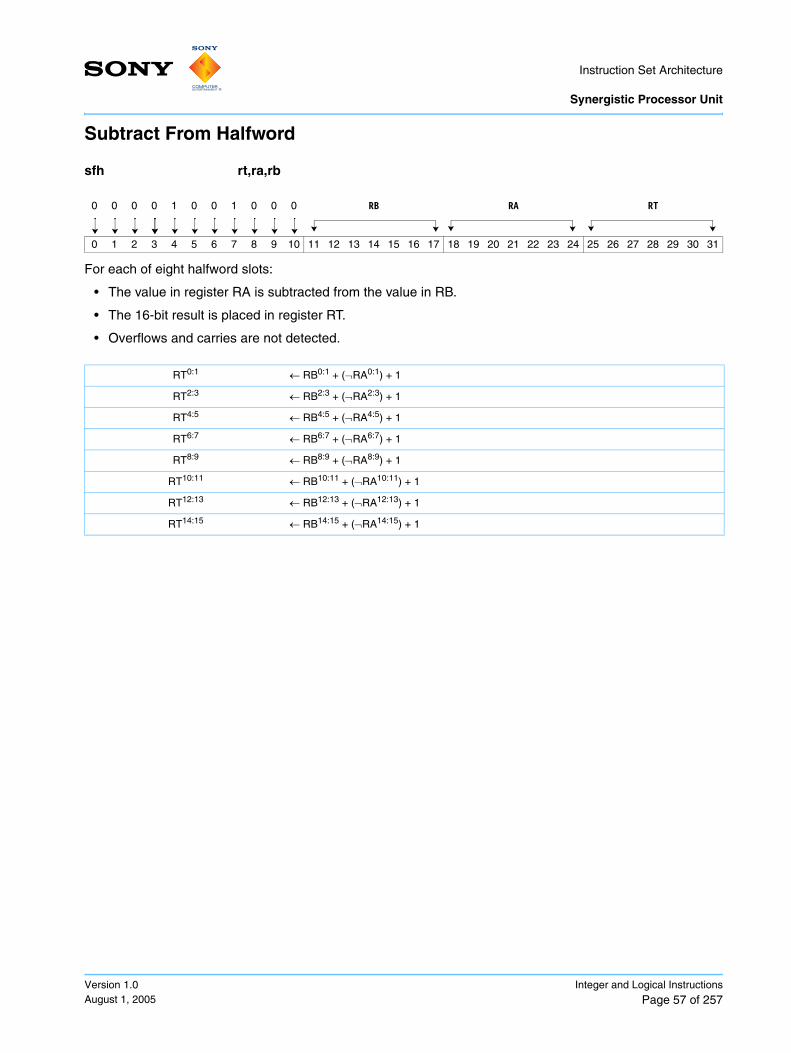
Instruction Set Architecture
Synergistic Processor Unit
Version 1.0August 1, 2005
Integer and Logical Instructions
Page 57 of 257
Subtract From Halfword
For each of eight halfword slots:
• The value in register RA is subtracted from the value in RB.
• The 16-bit result is placed in register RT.
• Overflows and carries are not detected.
sfh rt,ra,rb
0 0 0 0 1 0 0 1 0 0 0 RB RA RT
0 1 2 3 4 5 6 7 8 9 10 11 12 13 14 15 16 17 18 19 20 21 22 23 24 25 26 27 28 29 30 31
RT0:1 ← RB0:1 + (¬RA0:1) + 1
RT2:3 ← RB2:3 + (¬RA2:3) + 1
RT4:5 ← RB4:5 + (¬RA4:5) + 1
RT6:7 ← RB6:7 + (¬RA6:7) + 1
RT8:9 ← RB8:9 + (¬RA8:9) + 1
RT10:11 ← RB10:11 + (¬RA10:11) + 1
RT12:13 ← RB12:13 + (¬RA12:13) + 1
RT14:15 ← RB14:15 + (¬RA14:15) + 1

Instruction Set Architecture Synergistic Processor Unit
Integer and Logical Instructions
Page 58 of 257Version 1.0
August 1, 2005
Subtract From Halfword Immediate
For each of eight halfword slots:
• The value in register RA is subtracted from the signed value in the I10 field.
• The 16-bit result is placed in register RT.
• Overflows are not detected.
Programming Note: Although there is no Subtract Halfword Immediate instruction, its effect can be achieved by using the Add Immediate Halfword with a negative immediate field.
sfhi rt,ra,value
0 0 0 0 1 1 0 1 I10 RA RT
0 1 2 3 4 5 6 7 8 9 10 11 12 13 14 15 16 17 18 19 20 21 22 23 24 25 26 27 28 29 30 31
t ← RepLeftBit(I10,16)
RT0:1 ← t + (¬RA0:1) + 1
RT2:3 ← t + (¬RA2:3) + 1
RT4:5 ← t + (¬RA4:5) + 1
RT6:7 ← t + (¬RA6:7) + 1
RT8:9 ← t + (¬RA8:9) + 1
RT10:11 ← t + (¬RA10:11) + 1
RT12:13 ← t + (¬RA12:13) + 1
RT14:15 ← t + (¬RA14:15) + 1

Instruction Set Architecture
Synergistic Processor Unit
Version 1.0August 1, 2005
Integer and Logical Instructions
Page 59 of 257
Subtract From Word
For each of four word slots:
• The value in register RA is subtracted from the value in register RB.
• The result is placed in register RT.
• Overflows and carries are not detected.
sf rt,ra,rb
0 0 0 0 1 0 0 0 0 0 0 RB RA RT
0 1 2 3 4 5 6 7 8 9 10 11 12 13 14 15 16 17 18 19 20 21 22 23 24 25 26 27 28 29 30 31
RT0:3 ← RB0:3 + (¬RA0:3) + 1
RT4:7 ← RB4:7 + (¬RA4:7) + 1
RT8:11 ← RB8:11 + (¬RA8:11) + 1
RT12:15 ← RB12:15 + (¬RA12:15) + 1

Instruction Set Architecture Synergistic Processor Unit
Integer and Logical Instructions
Page 60 of 257Version 1.0
August 1, 2005
Subtract From Word Immediate
For each of four word slots:
• The value in register RA is subtracted from the value in the I10 field.
• The result is placed in register RT.
• Overflows and carries are not detected.
Programming Note: Although there is no Subtract Immediate instruction, its effect can be achieved by using the Add Immediate with a negative immediate field.
sfi rt,ra,value
0 0 0 0 1 1 0 0 I10 RA RT
0 1 2 3 4 5 6 7 8 9 10 11 12 13 14 15 16 17 18 19 20 21 22 23 24 25 26 27 28 29 30 31
t ← RepLeftBit(I10,32)
RT0:3 ← t + (¬RA0:3) + 1
RT4:7 ← t + (¬RA4:7) + 1
RT8:11 ← t + (¬RA8:11) + 1
RT12:15 ← t + (¬RA12:15) + 1

Instruction Set Architecture
Synergistic Processor Unit
Version 1.0August 1, 2005
Integer and Logical Instructions
Page 61 of 257
Add Extended
For each of four word slots:
• The operand from register RA is added to the operand from register RB and the least-significant bit of the operand from register RT.
• The 32-bit result is placed in register RT. Bits 0 to 30 of the RT input are reserved and should be zero.
addx rt,ra,rb
0 1 1 0 1 0 0 0 0 0 0 RB RA RT
0 1 2 3 4 5 6 7 8 9 10 11 12 13 14 15 16 17 18 19 20 21 22 23 24 25 26 27 28 29 30 31
RT0:3 ← RA0:3 + RB0:3 + RT31
RT4:7 ← RA4:7 + RB4:7 + RT63
RT8:11 ← RA8:11 + RB8:11 + RT95
RT12:15 ← RA12:15 + RB12:15 + RT127

Instruction Set Architecture Synergistic Processor Unit
Integer and Logical Instructions
Page 62 of 257Version 1.0
August 1, 2005
Carry Generate
For each of four word slots:
• The operand from register RA is added to the operand from register RB.
• The carry-out is placed in the least-significant bit of register RT.
• The remaining bits of RT are set to zero.
cg rt,ra,rb
0 0 0 1 1 0 0 0 0 1 0 RB RA RT
0 1 2 3 4 5 6 7 8 9 10 11 12 13 14 15 16 17 18 19 20 21 22 23 24 25 26 27 28 29 30 31
For j = 0 to 15 by 4t0:32 = ((0 || RAj::4) + (0 || RBj::4)) RTj::4 ← 310 || t0
End

Instruction Set Architecture
Synergistic Processor Unit
Version 1.0August 1, 2005
Integer and Logical Instructions
Page 63 of 257
Carry Generate Extended
For each of four word slots:
• The operand from register RA is added to the operand from register RB and the least-significant bit of register RT.
• The carry-out is placed in the least-significant bit of register RT.
• The remaining bits of RT are set to zero. Bits 0 to 30 of the RT input are reserved and should be zero.
cgx rt,ra,rb
0 1 1 0 1 0 0 0 0 1 0 RB RA RT
0 1 2 3 4 5 6 7 8 9 10 11 12 13 14 15 16 17 18 19 20 21 22 23 24 25 26 27 28 29 30 31
For j = 0 to 15 by 4t0:32 = (0 || RAj::4) + (0 || RBj::4) + (320 || RTj * 8 + 31) RTj::4 ← 310 || t0
End

Instruction Set Architecture Synergistic Processor Unit
Integer and Logical Instructions
Page 64 of 257Version 1.0
August 1, 2005
Subtract From Extended
For each of four word slots:
• The operand from register RA is subtracted from the operand from register RB. An additional ‘1’ is sub-tracted from the result if the least-significant bit of RT is ‘0’.
• The 32-bit result is placed in register RT. Bits 0 to 30 of the RT input are reserved and should be zero.
sfx rt,ra,rb
0 1 1 0 1 0 0 0 0 0 1 RB RA RT
0 1 2 3 4 5 6 7 8 9 10 11 12 13 14 15 16 17 18 19 20 21 22 23 24 25 26 27 28 29 30 31
RT0:3 ← RB0:3 + (¬RA0:3) + RT31
RT4:7 ← RB4:7 + (¬RA4:7) + RT63
RT8:11 ← RB8:11 + (¬RA8:11) + RT95
RT12:15 ← RB12:15 + (¬RA12:15) + RT127

Instruction Set Architecture
Synergistic Processor Unit
Version 1.0August 1, 2005
Integer and Logical Instructions
Page 65 of 257
Borrow Generate
For each of four word slots:
• If the unsigned value of RA is greater than the unsigned value of RB, then ‘0’ is placed in register RT. Oth-erwise, ‘1’ is placed in register RT.
bg rt,ra,rb
0 0 0 0 1 0 0 0 0 1 0 RB RA RT
0 1 2 3 4 5 6 7 8 9 10 11 12 13 14 15 16 17 18 19 20 21 22 23 24 25 26 27 28 29 30 31
For j = 0 to 15 by 4if (RBj::4 ≥u RAj::4) then RTj::4 ← 1else RTj::4 ← 0
End
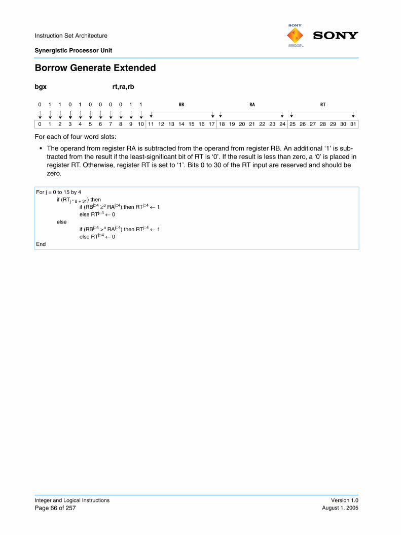
Instruction Set Architecture Synergistic Processor Unit
Integer and Logical Instructions
Page 66 of 257Version 1.0
August 1, 2005
Borrow Generate Extended
For each of four word slots:
• The operand from register RA is subtracted from the operand from register RB. An additional ‘1’ is sub-tracted from the result if the least-significant bit of RT is ‘0’. If the result is less than zero, a ‘0’ is placed in register RT. Otherwise, register RT is set to ‘1’. Bits 0 to 30 of the RT input are reserved and should be zero.
bgx rt,ra,rb
0 1 1 0 1 0 0 0 0 1 1 RB RA RT
0 1 2 3 4 5 6 7 8 9 10 11 12 13 14 15 16 17 18 19 20 21 22 23 24 25 26 27 28 29 30 31
For j = 0 to 15 by 4if (RTj * 8 + 31) then
if (RBj::4 ≥u RAj::4) then RTj::4 ← 1else RTj::4 ← 0
else if (RBj::4 >u RAj::4) then RTj::4 ← 1else RTj::4 ← 0
End
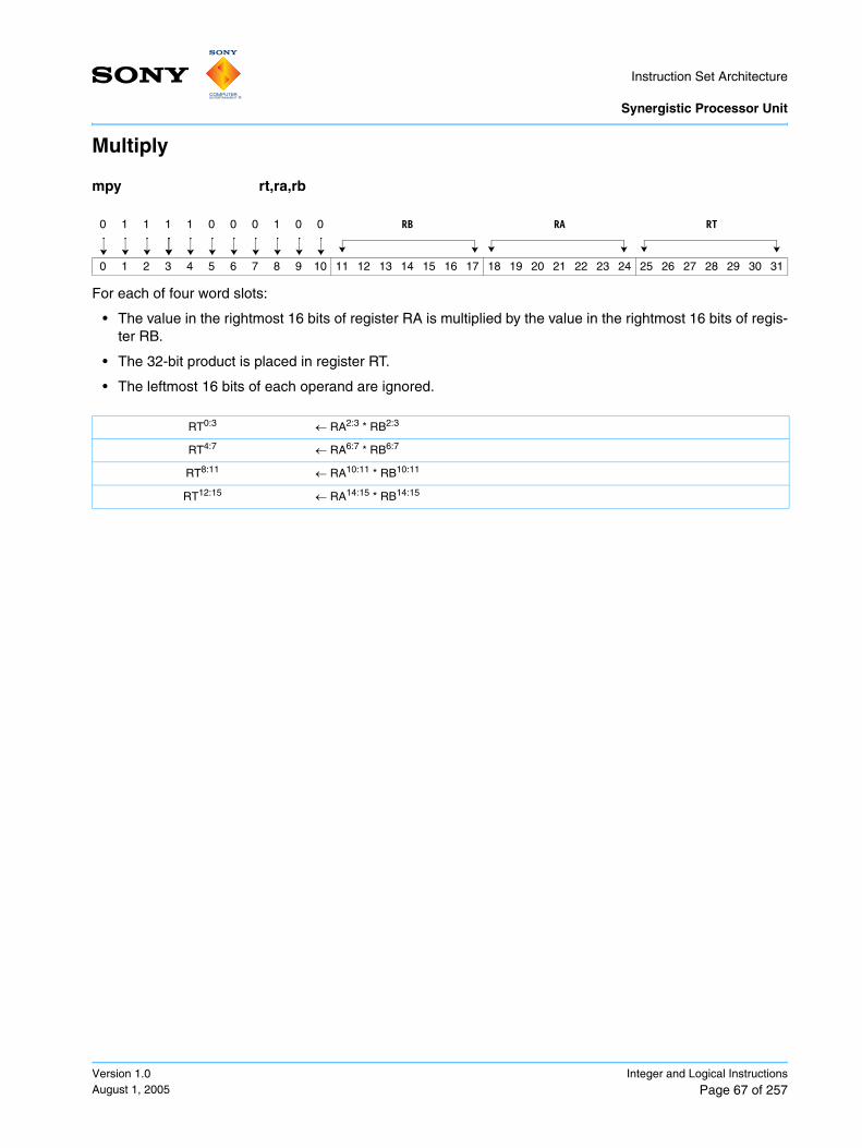
Instruction Set Architecture
Synergistic Processor Unit
Version 1.0August 1, 2005
Integer and Logical Instructions
Page 67 of 257
Multiply
For each of four word slots:
• The value in the rightmost 16 bits of register RA is multiplied by the value in the rightmost 16 bits of regis-ter RB.
• The 32-bit product is placed in register RT.
• The leftmost 16 bits of each operand are ignored.
mpy rt,ra,rb
0 1 1 1 1 0 0 0 1 0 0 RB RA RT
0 1 2 3 4 5 6 7 8 9 10 11 12 13 14 15 16 17 18 19 20 21 22 23 24 25 26 27 28 29 30 31
RT0:3 ← RA2:3 * RB2:3
RT4:7 ← RA6:7 * RB6:7
RT8:11 ← RA10:11 * RB10:11
RT12:15 ← RA14:15 * RB14:15

Instruction Set Architecture Synergistic Processor Unit
Integer and Logical Instructions
Page 68 of 257Version 1.0
August 1, 2005
Multiply Unsigned
For each of four word slots:
• The rightmost 16 bits of register RA are multiplied by the rightmost 16 bits of register RB, treating both operands as unsigned.
• The 32-bit product is placed in register RT.
mpyu rt,ra,rb
0 1 1 1 1 0 0 1 1 0 0 RB RA RT
0 1 2 3 4 5 6 7 8 9 10 11 12 13 14 15 16 17 18 19 20 21 22 23 24 25 26 27 28 29 30 31
RT0:3 ← RA2:3 |*| RB2:3
RT4:7 ← RA6:7 |*| RB6:7
RT8:11 ← RA10:11 |*| RB10:11
RT12:15 ← RA14:15 |*| RB14:15

Instruction Set Architecture
Synergistic Processor Unit
Version 1.0August 1, 2005
Integer and Logical Instructions
Page 69 of 257
Multiply Immediate
For each of four word slots:
• The signed value in the I10 field is multiplied by the value in the rightmost 16 bits of register RA.
• The resulting product is placed in register RT.
mpyi rt,ra,value
0 1 1 1 0 1 0 0 I10 RA RT
0 1 2 3 4 5 6 7 8 9 10 11 12 13 14 15 16 17 18 19 20 21 22 23 24 25 26 27 28 29 30 31
t ← RepLeftBit(I10,16)
RT0:3 ← RA2:3 * t
RT4:7 ← RA6:7 * t
RT8:11 ← RA10:11 * t
RT12:15 ← RA14:15 * t

Instruction Set Architecture Synergistic Processor Unit
Integer and Logical Instructions
Page 70 of 257Version 1.0
August 1, 2005
Multiply Unsigned Immediate
For each of four word slots:
• The signed value in the I10 field is extended to 16 bits by replicating the leftmost bit. The resulting value is multiplied by the rightmost 16 bits of register RA, treating both operands as unsigned.
• The resulting product is placed in register RT.
mpyui rt,ra,value
0 1 1 1 0 1 0 1 I10 RA RT
0 1 2 3 4 5 6 7 8 9 10 11 12 13 14 15 16 17 18 19 20 21 22 23 24 25 26 27 28 29 30 31
t ← RepLeftBit(I10,16)
RT0:3 ← RA2:3 |*| t
RT4:7 ← RA6:7 |*| t
RT8:11 ← RA10:11 |*| t
RT12:15 ← RA14:15 |*| t

Instruction Set Architecture
Synergistic Processor Unit
Version 1.0August 1, 2005
Integer and Logical Instructions
Page 71 of 257
Multiply and Add
For each of four word slots:
• The value in register RA is treated as a 16-bit signed integer and multiplied by the 16-bit signed value in register RB. The resulting product is added to the value in register RC.
• The result is placed in register RT.
• Overflows and carries are not detected.
Programming Note: The operands are right-aligned within the 32-bit field.
mpya rt,ra,rb,rc
1 1 0 0 RT RB RA RC
0 1 2 3 4 5 6 7 8 9 10 11 12 13 14 15 16 17 18 19 20 21 22 23 24 25 26 27 28 29 30 31
t0 ← RA2:3 * RB2:3
t1 ← RA6:7 * RB6:7
t2 ← RA10:11 * RB10:11
t3 ← RA14:15 * RB14:15
RT0:3 ← t0 + RC0:3
RT4:7 ← t1 + RC4:7
RT8:11 ← t2 + RC8:11
RT12:15 ← t3 + RC12:15

Instruction Set Architecture Synergistic Processor Unit
Integer and Logical Instructions
Page 72 of 257Version 1.0
August 1, 2005
Multiply High
For each of four word slots:
• The leftmost 16 bits of the value in register RA are shifted right by 16 bits and multiplied by the 16-bit value in register RB.
• The product is shifted left by 16 bits and placed in register RT. Bits shifted out at the left are discarded. Zeros are shifted in at the right.
Programming Note: This instruction can be used in conjunction with mpyu and add to perform a 32-bit multiply.
mpyh rt,ra,rb
0 1 1 1 1 0 0 0 1 0 1 RB RA RT
0 1 2 3 4 5 6 7 8 9 10 11 12 13 14 15 16 17 18 19 20 21 22 23 24 25 26 27 28 29 30 31
t0 ← RA0:1 * RB2:3
t1 ← RA4:5 * RB6:7
t2 ← RA8:9 * RB10:11
t3 ← RA12:13 * RB14:15
RT0:3 ← t02:3 || 0x0000
RT4:7 ← t12:3 || 0x0000
RT8:11 ← t22:3 || 0x0000
RT12:15 ← t32:3 || 0x0000

Instruction Set Architecture
Synergistic Processor Unit
Version 1.0August 1, 2005
Integer and Logical Instructions
Page 73 of 257
Multiply and Shift Right
For each of four word slots:
• The value in the rightmost 16 bits of register RA is multiplied by the value in the rightmost 16 bits of regis-ter RB.
• The leftmost 16 bits of the 32-bit product are placed in the rightmost 16 bits of register RT, with the sign bit replicated into the left 16 bits of the register.
mpys rt,ra,rb
0 1 1 1 1 0 0 0 1 1 1 RB RA RT
0 1 2 3 4 5 6 7 8 9 10 11 12 13 14 15 16 17 18 19 20 21 22 23 24 25 26 27 28 29 30 31
t0 ← RA2:3 * RB2:3
t1 ← RA6:7 * RB6:7
t2 ← RA10:11 * RB10:11
t3 ← RA14:15 * RB14:15
RT0:3 ← RepLeftBit(t00:1,32)
RT4:7 ← RepLeftBit(t10:1,32)
RT8:11 ← RepLeftBit(t20:1,32)
RT12:15 ← RepLeftBit(t30:1,32)

Instruction Set Architecture Synergistic Processor Unit
Integer and Logical Instructions
Page 74 of 257Version 1.0
August 1, 2005
Multiply High High
For each of four word slots:
• The leftmost 16 bits in register RA are multiplied by the leftmost 16 bits in register RB.
• The 32-bit product is placed in register RT.
mpyhh rt,ra,rb
0 1 1 1 1 0 0 0 1 1 0 RB RA RT
0 1 2 3 4 5 6 7 8 9 10 11 12 13 14 15 16 17 18 19 20 21 22 23 24 25 26 27 28 29 30 31
RT0:3 ← RA0:1 * RB0:1
RT4:7 ← RA4:5 * RB4:5
RT8:11 ← RA8:9 * RB8:9
RT12:15 ← RA12:13 * RB12:13

Instruction Set Architecture
Synergistic Processor Unit
Version 1.0August 1, 2005
Integer and Logical Instructions
Page 75 of 257
Multiply High High and Add
For each of four word slots:
• The leftmost 16 bits in register RA are multiplied by the leftmost 16 bits in register RB. The product is added to the value in register RT.
• The sum is placed in register RT.
mpyhha rt,ra,rb
0 1 1 0 1 0 0 0 1 1 0 RB RA RT
0 1 2 3 4 5 6 7 8 9 10 11 12 13 14 15 16 17 18 19 20 21 22 23 24 25 26 27 28 29 30 31
RT0:3 ← RA0:1 * RB0:1 + RT0:3
RT4:7 ← RA4:5 * RB4:5 + RT4:7
RT8:11 ← RA8:9 * RB8:9+ RT8:11
RT12:15 ← RA12:13 * RB12:13 + RT12:15

Instruction Set Architecture Synergistic Processor Unit
Integer and Logical Instructions
Page 76 of 257Version 1.0
August 1, 2005
Multiply High High Unsigned
For each of four word slots:
• The leftmost 16 bits in register RA are multiplied by the leftmost 16 bits in register RB, treating both oper-ands as unsigned.
• The 32-bit product is placed in register RT.
mpyhhu rt,ra,rb
0 1 1 1 1 0 0 1 1 1 0 RB RA RT
0 1 2 3 4 5 6 7 8 9 10 11 12 13 14 15 16 17 18 19 20 21 22 23 24 25 26 27 28 29 30 31
RT0:3 ← RA0:1 |*| RB0:1
RT4:7 ← RA4:5 |*| RB4:5
RT8:11 ← RA8:9 |*| RB8:9
RT12:15 ← RA12:13 |*| RB12:13
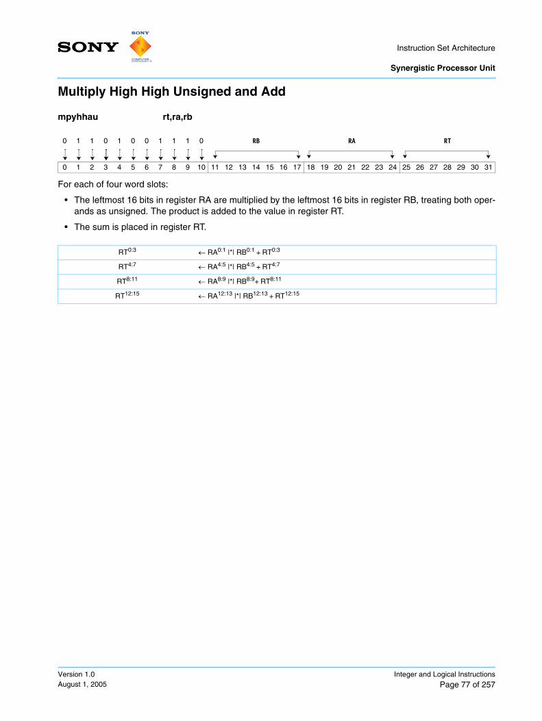
Instruction Set Architecture
Synergistic Processor Unit
Version 1.0August 1, 2005
Integer and Logical Instructions
Page 77 of 257
Multiply High High Unsigned and Add
For each of four word slots:
• The leftmost 16 bits in register RA are multiplied by the leftmost 16 bits in register RB, treating both oper-ands as unsigned. The product is added to the value in register RT.
• The sum is placed in register RT.
mpyhhau rt,ra,rb
0 1 1 0 1 0 0 1 1 1 0 RB RA RT
0 1 2 3 4 5 6 7 8 9 10 11 12 13 14 15 16 17 18 19 20 21 22 23 24 25 26 27 28 29 30 31
RT0:3 ← RA0:1 |*| RB0:1 + RT0:3
RT4:7 ← RA4:5 |*| RB4:5 + RT4:7
RT8:11 ← RA8:9 |*| RB8:9+ RT8:11
RT12:15 ← RA12:13 |*| RB12:13 + RT12:15

Instruction Set Architecture Synergistic Processor Unit
Integer and Logical Instructions
Page 78 of 257Version 1.0
August 1, 2005
Count Leading Zeros
For each of four word slots:
• The number of zero bits to the left of the first ‘1’ bit in the operand in register RA is computed.
• The result is placed in register RT. If register RA is zero, the result is 32.
Programming Note: The result placed in register RT satisfies 0 ≤ RT ≤ 32. The value in register RT is zero, for example, if the corresponding slot in RA is a negative integer. The value in register RT is 32 if the corre-sponding slot in register RA is zero.
clz rt,ra
0 1 0 1 0 1 0 0 1 0 1 /// RA RT
0 1 2 3 4 5 6 7 8 9 10 11 12 13 14 15 16 17 18 19 20 21 22 23 24 25 26 27 28 29 30 31
For i = 0 to 3t ← 0; j ← i * 4u ← RAj::4
For m = 0 to 31If um = 1 then leavet ← t + 1
EndRTj::4 ← t
End

Instruction Set Architecture
Synergistic Processor Unit
Version 1.0August 1, 2005
Integer and Logical Instructions
Page 79 of 257
Count Ones in Bytes
For each of 16 byte slots:
• The number of bits in register RA whose value is ‘1’ is computed.
• The result is placed in register RT.
Programming Note: The result placed in register RT satisfies 0 ≤ RT ≤ 8. The value in register RT is zero, for example, if the value in RA is zero. The value in RT is 8 if the value in RA is -1.
(See also the Form Select Mask for Bytes instruction on page 80.)
cntb rt,ra
0 1 0 1 0 1 1 0 1 0 0 /// RA RT
0 1 2 3 4 5 6 7 8 9 10 11 12 13 14 15 16 17 18 19 20 21 22 23 24 25 26 27 28 29 30 31
For j = 0 to 15c = 0 b ← RAj
For m = 0 to 7If bm = 1 then c ← c + 1
EndRTj ← c
End

Instruction Set Architecture Synergistic Processor Unit
Integer and Logical Instructions
Page 80 of 257Version 1.0
August 1, 2005
Form Select Mask for Bytes
The rightmost 16 bits of the preferred slot of register RA are used to create a mask in register RT by replicating each bit eight times. Bits in the operand are related to bytes in the result in a left-to-right correspondence.
fsmb rt,ra
0 0 1 1 0 1 1 0 1 1 0 /// RA RT
0 1 2 3 4 5 6 7 8 9 10 11 12 13 14 15 16 17 18 19 20 21 22 23 24 25 26 27 28 29 30 31
s ← RA2:3 & 0x0FFFFFor j = 0 to 15If sj
= 0 then rj ← 0x00 elserj ← 0xFF
EndRT ← r

Instruction Set Architecture
Synergistic Processor Unit
Version 1.0August 1, 2005
Integer and Logical Instructions
Page 81 of 257
Form Select Mask for Halfwords
The rightmost 8 bits of the preferred slot of register RA are used to create a mask in register RT by replicating each bit 16 times. Bits in the operand are related to halfwords in the result, in a left-to-right correspondence.
fsmh rt,ra
0 0 1 1 0 1 1 0 1 0 1 /// RA RT
0 1 2 3 4 5 6 7 8 9 10 11 12 13 14 15 16 17 18 19 20 21 22 23 24 25 26 27 28 29 30 31
s ← RA3 k = 0For j = 0 to 7
If sj = 0 then rk::2 ← 0x0000 else
rk::2 ← 0xFFFFk = k + 2
EndRT ← r

Instruction Set Architecture Synergistic Processor Unit
Integer and Logical Instructions
Page 82 of 257Version 1.0
August 1, 2005
Form Select Mask for Words
The rightmost 4 bits of the preferred slot of register RA are used to create a mask in register RT by replicating each bit 32 times. Bits in the operand are related to words in the result in a left-to-right correspondence.
fsm rt,ra
0 0 1 1 0 1 1 0 1 0 0 /// RA RT
0 1 2 3 4 5 6 7 8 9 10 11 12 13 14 15 16 17 18 19 20 21 22 23 24 25 26 27 28 29 30 31
s ← RA28:31 k = 0For j = 0 to 3
If sj = 0 then rk::4 ← 0x00000000 else
rk::4 ← 0xFFFFFFFFk = k + 4End
RT ← r

Instruction Set Architecture
Synergistic Processor Unit
Version 1.0August 1, 2005
Integer and Logical Instructions
Page 83 of 257
Gather Bits from Bytes
A 16-bit quantity is formed in the right half of the preferred slot of register RT by concatenating the rightmost bit in each byte of register RA. The leftmost 16 bits of register RT are set to zero, as are the remaining slots of register RT.
gbb rt,ra
0 0 1 1 0 1 1 0 0 1 0 /// RA RT
0 1 2 3 4 5 6 7 8 9 10 11 12 13 14 15 16 17 18 19 20 21 22 23 24 25 26 27 28 29 30 31
k = 0s = 0For j = 7 to 128 by 8
sk ← RAjk = k + 1End
RT0:3 ← 0x0000 || sRT4:7 ← 0RT8:11 ← 0RT12:15 ← 0

Instruction Set Architecture Synergistic Processor Unit
Integer and Logical Instructions
Page 84 of 257Version 1.0
August 1, 2005
Gather Bits from Halfwords
An 8-bit quantity is formed in the rightmost byte of the preferred slot of register RT by concatenating the right-most bit in each halfword of register RA. The leftmost 24 bits of the preferred slot of register RT are set to zero, as are the remaining slots of register RT.
gbh rt,ra
0 0 1 1 0 1 1 0 0 0 1 /// RA RT
0 1 2 3 4 5 6 7 8 9 10 11 12 13 14 15 16 17 18 19 20 21 22 23 24 25 26 27 28 29 30 31
k = 8s = 0For j = 15 to 128 by 16
sk ← RAjk = k + 1End
RT0:3 ← 0x0000 || sRT4:7 ← 0RT8:11 ← 0RT12:15 ← 0

Instruction Set Architecture
Synergistic Processor Unit
Version 1.0August 1, 2005
Integer and Logical Instructions
Page 85 of 257
Gather Bits from Words
A 4-bit quantity is formed in the rightmost 4 bits of register RT by concatenating the rightmost bit in each word of register RA. The leftmost 28 bits of register RT are set to zero, as are the remaining slots of register RT.
gb rt,ra
0 0 1 1 0 1 1 0 0 0 0 /// RA RT
0 1 2 3 4 5 6 7 8 9 10 11 12 13 14 15 16 17 18 19 20 21 22 23 24 25 26 27 28 29 30 31
k = 12s = 0
For j = 31 to 128 by 32sk ← RAjk ← k +1End
RT0:3 ← 0x0000 || sRT4:7 ← 0RT8:11 ← 0RT12:15 ← 0

Instruction Set Architecture Synergistic Processor Unit
Integer and Logical Instructions
Page 86 of 257Version 1.0
August 1, 2005
Average Bytes
For each of 16 byte slots:
• The operand from register RA is added to the operand from register RB, and ‘1’ is added to the result. These additions are done without loss of precision.
• That result is shifted to the right by 1 bit and placed in register RT.
avgb rt,ra,rb
0 0 0 1 1 0 1 0 0 1 1 RB RA RT
0 1 2 3 4 5 6 7 8 9 10 11 12 13 14 15 16 17 18 19 20 21 22 23 24 25 26 27 28 29 30 31
For j = 0 to 15RTj ← ((0x00 || RAj) + (0x00 || RBj) + 1)7:14
End
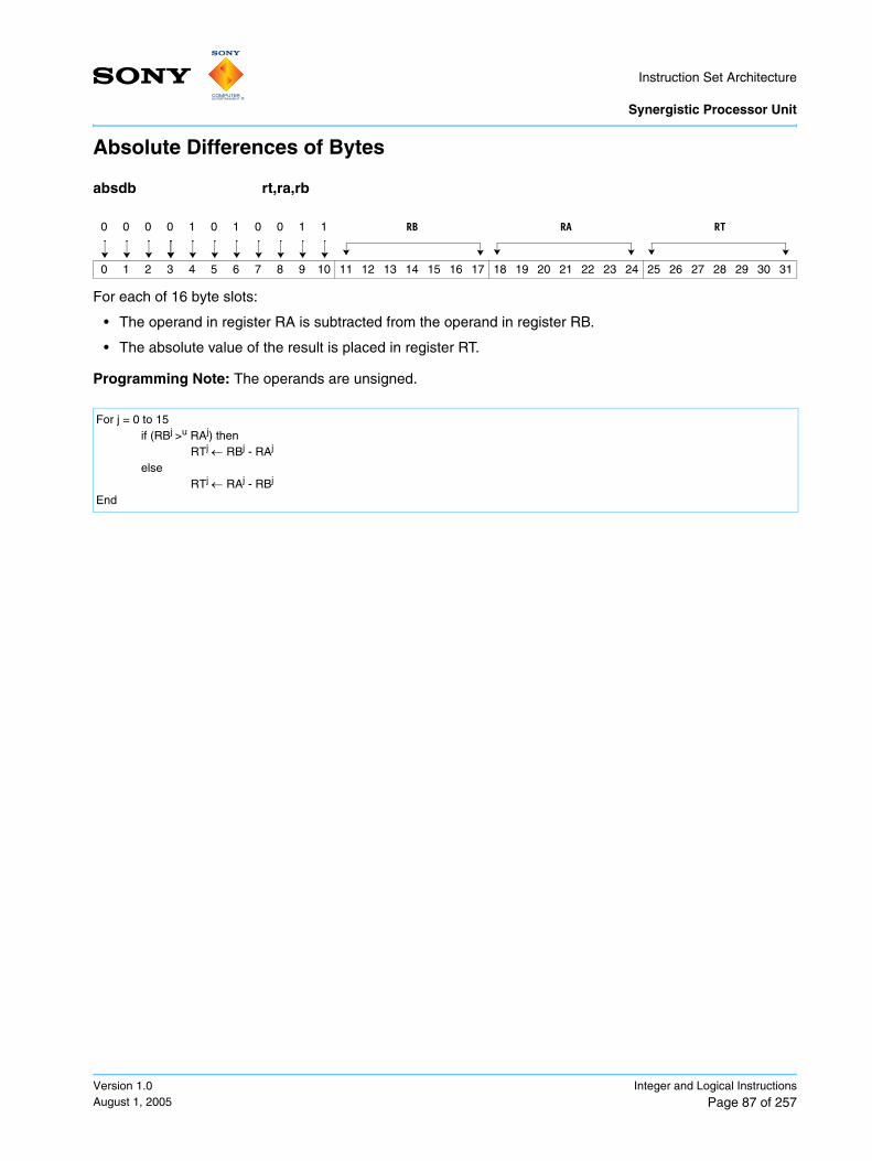
Instruction Set Architecture
Synergistic Processor Unit
Version 1.0August 1, 2005
Integer and Logical Instructions
Page 87 of 257
Absolute Differences of Bytes
For each of 16 byte slots:
• The operand in register RA is subtracted from the operand in register RB.
• The absolute value of the result is placed in register RT.
Programming Note: The operands are unsigned.
absdb rt,ra,rb
0 0 0 0 1 0 1 0 0 1 1 RB RA RT
0 1 2 3 4 5 6 7 8 9 10 11 12 13 14 15 16 17 18 19 20 21 22 23 24 25 26 27 28 29 30 31
For j = 0 to 15if (RBj >u RAj) then
RTj ← RBj - RAj
elseRTj ← RAj - RBj
End

Instruction Set Architecture Synergistic Processor Unit
Integer and Logical Instructions
Page 88 of 257Version 1.0
August 1, 2005
Sum Bytes into Halfwords
For each of four word slots:
• The 4 bytes in register RB are added, and the 16-bit result is placed in bytes 0 and 1 of register RT.
• The 4 bytes in register RA are added, and the 16-bit result is placed in bytes 2 and 3 of register RT.
Programming Note: The operands are unsigned.
sumb rt,ra,rb
0 1 0 0 1 0 1 0 0 1 1 RB RA RT
0 1 2 3 4 5 6 7 8 9 10 11 12 13 14 15 16 17 18 19 20 21 22 23 24 25 26 27 28 29 30 31
RT0:1 ← RB0 + RB1+ RB2 + RB3
RT2:3 ← RA0 + RA1+ RA2 + RA3
RT4:5 ← RB4 + RB5+ RB6 + RB7
RT6:7 ← RA4 + RA5+ RA6 + RA7
RT8:9 ← RB8 + RB9+ RB10 + RB11
RT10:11 ← RA8 + RA9+ RA10 + RA11
RT12:13 ← RB12 + RB13+ RB14 + RB15
RT14:15 ← RA12 + RA13+ RA14 + RA15

Instruction Set Architecture
Synergistic Processor Unit
Version 1.0August 1, 2005
Integer and Logical Instructions
Page 89 of 257
Extend Sign Byte to Halfword
For each of eight halfword slots:
• The sign of the byte in the right byte of the operand in register RA is propagated to the left byte.
• The resulting 16-bit integer is stored in register RT.
Programming Note: This is the only instruction that treats bytes as signed.
xsbh rt,ra
0 1 0 1 0 1 1 0 1 1 0 /// RA RT
0 1 2 3 4 5 6 7 8 9 10 11 12 13 14 15 16 17 18 19 20 21 22 23 24 25 26 27 28 29 30 31
RT0:1 ← RepLeftBit(RA1,16)
RT2:3 ← RepLeftBit(RA3,16)
RT4:5 ← RepLeftBit(RA5,16)
RT6:7 ← RepLeftBit(RA7,16)
RT8:9 ← RepLeftBit(RA9,16)
RT10:11 ← RepLeftBit(RA11,16)
RT12:13 ← RepLeftBit(RA13,16)
RT14:15 ← RepLeftBit(RA15,16)

Instruction Set Architecture Synergistic Processor Unit
Integer and Logical Instructions
Page 90 of 257Version 1.0
August 1, 2005
Extend Sign Halfword to Word
For each of four word slots:
• The sign of the halfword in the right half of the operand in register RA is propagated to the left halfword.
• The resulting 32-bit integer is placed in register RT.
xshw rt,ra
0 1 0 1 0 1 0 1 1 1 0 /// RA RT
0 1 2 3 4 5 6 7 8 9 10 11 12 13 14 15 16 17 18 19 20 21 22 23 24 25 26 27 28 29 30 31
RT0:3 ← RepLeftBit(RA2:3,32)
RT4:7 ← RepLeftBit(RA6:7,32)
RT8:11 ← RepLeftBit(RA10:11,32)
RT12:15 ← RepLeftBit(RA14:15,32)

Instruction Set Architecture
Synergistic Processor Unit
Version 1.0August 1, 2005
Integer and Logical Instructions
Page 91 of 257
Extend Sign Word to Doubleword
For each of two doubleword slots:
• The sign of the word in the right slot is propagated to the left word.
• The resulting 64-bit integer is stored in register RT.
xswd rt,ra
0 1 0 1 0 1 0 0 1 1 0 /// RA RT
0 1 2 3 4 5 6 7 8 9 10 11 12 13 14 15 16 17 18 19 20 21 22 23 24 25 26 27 28 29 30 31
RT0:7 ← RepLeftBit(RA4:7,64)
RT8:15 ← RepLeftBit(RA12:15,64)

Instruction Set Architecture Synergistic Processor Unit
Integer and Logical Instructions
Page 92 of 257Version 1.0
August 1, 2005
And
The values in register RA and register RB are logically ANDed. The result is placed in register RT.
and rt,ra,rb
0 0 0 1 1 0 0 0 0 0 1 RB RA RT
0 1 2 3 4 5 6 7 8 9 10 11 12 13 14 15 16 17 18 19 20 21 22 23 24 25 26 27 28 29 30 31
RT0:3 ← RA0:3 & RB0:3
RT4:7 ← RA4:7 & RB4:7
RT8:11 ← RA8:11 & RB8:11
RT12:15 ← RA12:15 & RB12:15

Instruction Set Architecture
Synergistic Processor Unit
Version 1.0August 1, 2005
Integer and Logical Instructions
Page 93 of 257
And with Complement
The value in register RA is logically ANDed with the complement of the value in register RB. The result is placed in register RT.
andc rt,ra,rb
0 1 0 1 1 0 0 0 0 0 1 RB RA RT
0 1 2 3 4 5 6 7 8 9 10 11 12 13 14 15 16 17 18 19 20 21 22 23 24 25 26 27 28 29 30 31
RT0:3 ← RA0:3 & (¬RB0:3)
RT4:7 ← RA4:7 & (¬RB4:7)
RT8:11 ← RA8:11 & (¬RB8:11)
RT12:15 ← RA12:15 & (¬RB12:15)
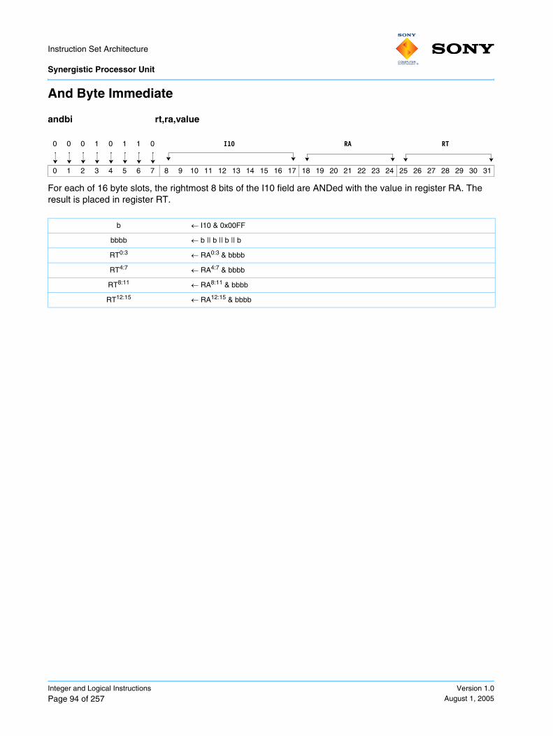
Instruction Set Architecture Synergistic Processor Unit
Integer and Logical Instructions
Page 94 of 257Version 1.0
August 1, 2005
And Byte Immediate
For each of 16 byte slots, the rightmost 8 bits of the I10 field are ANDed with the value in register RA. The result is placed in register RT.
andbi rt,ra,value
0 0 0 1 0 1 1 0 I10 RA RT
0 1 2 3 4 5 6 7 8 9 10 11 12 13 14 15 16 17 18 19 20 21 22 23 24 25 26 27 28 29 30 31
b ← I10 & 0x00FF
bbbb ← b || b || b || b
RT0:3 ← RA0:3 & bbbb
RT4:7 ← RA4:7 & bbbb
RT8:11 ← RA8:11 & bbbb
RT12:15 ← RA12:15 & bbbb

Instruction Set Architecture
Synergistic Processor Unit
Version 1.0August 1, 2005
Integer and Logical Instructions
Page 95 of 257
And Halfword Immediate
For each of eight halfword slots:
• The I10 field is extended to 16 bits by replicating its leftmost bit. The result is ANDed with the value in reg-ister RA.
• The 16-bit result is placed in register RT.
andhi rt,ra,value
0 0 0 1 0 1 0 1 I10 RA RT
0 1 2 3 4 5 6 7 8 9 10 11 12 13 14 15 16 17 18 19 20 21 22 23 24 25 26 27 28 29 30 31
t ← RepLeftBit(I10,16)
RT0:1 ← RA0:1 & t
RT2:3 ← RA2:3 & t
RT4:5 ← RA4:5 & t
RT6:7 ← RA6:7 & t
RT8:9 ← RA8:9 & t
RT10:11 ← RA10:11 & t
RT12:13 ← RA12:13 & t
RT14:15 ← RA14:15 & t

Instruction Set Architecture Synergistic Processor Unit
Integer and Logical Instructions
Page 96 of 257Version 1.0
August 1, 2005
And Word Immediate
For each of four word slots:
• The value of the I10 field is extended to 32 bits by replicating its leftmost bit. The result is ANDed with the contents of register RA.
• The result is placed in register RT.
andi rt,ra,value
0 0 0 1 0 1 0 0 I10 RA RT
0 1 2 3 4 5 6 7 8 9 10 11 12 13 14 15 16 17 18 19 20 21 22 23 24 25 26 27 28 29 30 31
t ← RepLeftBit(I10,32)
RT0:3 ← RA0:3 & t
RT4:7 ← RA4:7 & t
RT8:11 ← RA8:11 & t
RT12:15 ← RA12:15 & t
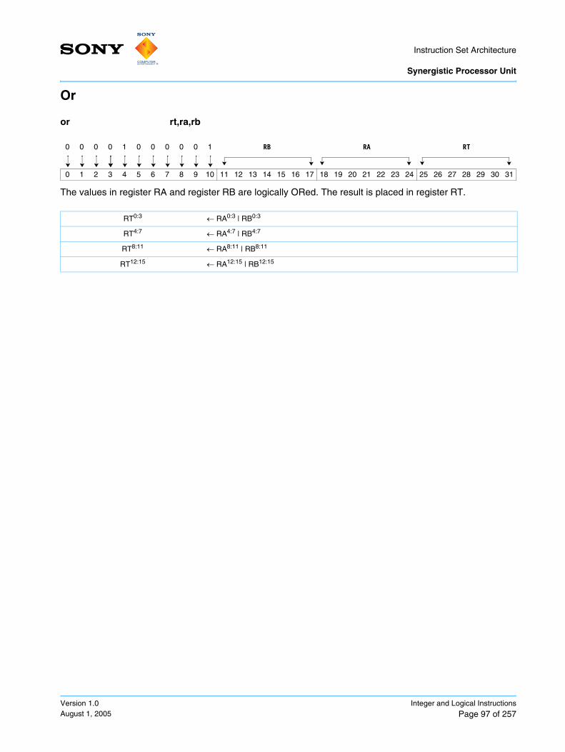
Instruction Set Architecture
Synergistic Processor Unit
Version 1.0August 1, 2005
Integer and Logical Instructions
Page 97 of 257
Or
The values in register RA and register RB are logically ORed. The result is placed in register RT.
or rt,ra,rb
0 0 0 0 1 0 0 0 0 0 1 RB RA RT
0 1 2 3 4 5 6 7 8 9 10 11 12 13 14 15 16 17 18 19 20 21 22 23 24 25 26 27 28 29 30 31
RT0:3 ← RA0:3 | RB0:3
RT4:7 ← RA4:7 | RB4:7
RT8:11 ← RA8:11 | RB8:11
RT12:15 ← RA12:15 | RB12:15

Instruction Set Architecture Synergistic Processor Unit
Integer and Logical Instructions
Page 98 of 257Version 1.0
August 1, 2005
Or with Complement
The value in register RA is ORed with the complement of the value in register RB. The result is placed in register RT.
orc rt,ra,rb
0 1 0 1 1 0 0 1 0 0 1 RB RA RT
0 1 2 3 4 5 6 7 8 9 10 11 12 13 14 15 16 17 18 19 20 21 22 23 24 25 26 27 28 29 30 31
RT0:3 ← RA0:3 | (¬RB0:3)
RT4:7 ← RA4:7 | (¬RB4:7)
RT8:11 ← RA8:11 | (¬RB8:11)
RT12:15 ← RA12:15 | (¬RB12:15)
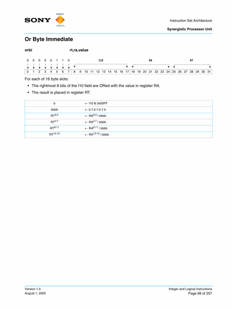
Instruction Set Architecture
Synergistic Processor Unit
Version 1.0August 1, 2005
Integer and Logical Instructions
Page 99 of 257
Or Byte Immediate
For each of 16 byte slots:
• The rightmost 8 bits of the I10 field are ORed with the value in register RA.
• The result is placed in register RT.
orbi rt,ra,value
0 0 0 0 0 1 1 0 I10 RA RT
0 1 2 3 4 5 6 7 8 9 10 11 12 13 14 15 16 17 18 19 20 21 22 23 24 25 26 27 28 29 30 31
b ← I10 & 0x00FF
bbbb ← b || b || b || b
RT0:3 ← RA0:3 | bbbb
RT4:7 ← RA4:7 | bbbb
RT8:11 ← RA8:11 | bbbb
RT12:15 ← RA12:15 | bbbb

Instruction Set Architecture Synergistic Processor Unit
Integer and Logical Instructions
Page 100 of 257Version 1.0
August 1, 2005
Or Halfword Immediate
For each of eight halfword slots:
• The I10 field is extended to 16 bits by replicating its leftmost bit. The result is ORed with the value in reg-ister RA.
• The result is placed in register RT.
orhi rt,ra,value
0 0 0 0 0 1 0 1 I10 RA RT
0 1 2 3 4 5 6 7 8 9 10 11 12 13 14 15 16 17 18 19 20 21 22 23 24 25 26 27 28 29 30 31
t ← RepLeftBit(I10,16)
RT0:1 ← RA0:1 | t
RT2:3 ← RA2:3 | t
RT4:5 ← RA4:5 | t
RT6:7 ← RA6:7 | t
RT8:9 ← RA8:9 | t
RT10:11 ← RA10:11 | t
RT12:13 ← RA12:13 | t
RT14:15 ← RA14:15 | t

Instruction Set Architecture
Synergistic Processor Unit
Version 1.0August 1, 2005
Integer and Logical Instructions
Page 101 of 257
Or Word Immediate
For each of four word slots:
• The I10 field is sign-extended to 32 bits and ORed with the contents of register RA.
• The result is placed in register RT.
ori rt,ra,value
0 0 0 0 0 1 0 0 I10 RA RT
0 1 2 3 4 5 6 7 8 9 10 11 12 13 14 15 16 17 18 19 20 21 22 23 24 25 26 27 28 29 30 31
t ← RepLeftBit(I10,32)
RT0:3 ← RA0:3 | t
RT4:7 ← RA4:7 | t
RT8:11 ← RA8:11 | t
RT12:15 ← RA12:15 | t

Instruction Set Architecture Synergistic Processor Unit
Integer and Logical Instructions
Page 102 of 257Version 1.0
August 1, 2005
Or Across
The four words of RA are logically ORed. The result is placed in the preferred slot of register RT. The other three slots of the register are written with zeros.
orx rt,ra
0 0 1 1 1 1 1 0 0 0 0 /// RA RT
0 1 2 3 4 5 6 7 8 9 10 11 12 13 14 15 16 17 18 19 20 21 22 23 24 25 26 27 28 29 30 31
RT0:3 ← RA0:3 | RA4:7 | RA8:11 | RA12:15
RT4:15 ← 0

Instruction Set Architecture
Synergistic Processor Unit
Version 1.0August 1, 2005
Integer and Logical Instructions
Page 103 of 257
Exclusive Or
The values in register RA and register RB are logically XORed. The result is placed in register RT.
xor rt,ra,rb
0 1 0 0 1 0 0 0 0 0 1 RB RA RT
0 1 2 3 4 5 6 7 8 9 10 11 12 13 14 15 16 17 18 19 20 21 22 23 24 25 26 27 28 29 30 31
RT0:3 ← RA0:3 ⊕ RB0:3
RT4:7 ← RA4:7 ⊕ RB4:7
RT8:11 ← RA8:11 ⊕ RB8:11
RT12:15 ← RA12:15 ⊕ RB12:15

Instruction Set Architecture Synergistic Processor Unit
Integer and Logical Instructions
Page 104 of 257Version 1.0
August 1, 2005
Exclusive Or Byte Immediate
For each of 16 byte slots:
• The rightmost 8 bits of the I10 field are XORed with the value in register RA.
• The result is placed in register RT.
xorbi rt,ra,value
0 1 0 0 0 1 1 0 I10 RA RT
0 1 2 3 4 5 6 7 8 9 10 11 12 13 14 15 16 17 18 19 20 21 22 23 24 25 26 27 28 29 30 31
b ← I10 & 0x00FF
bbbb ← b || b || b || b
RT0:3 ← RA0:3 ⊕ bbbb
RT4:7 ← RA4:7 ⊕ bbbb
RT8:11 ← RA8:11 ⊕ bbbb
RT12:15 ← RA12:15 ⊕ bbbb

Instruction Set Architecture
Synergistic Processor Unit
Version 1.0August 1, 2005
Integer and Logical Instructions
Page 105 of 257
Exclusive Or Halfword Immediate
For each of eight halfword slots:
• The I10 field is extended to 16 bits by replicating the leftmost bit. The resulting value is XORed with the value in register RA.
• The 16-bit result is placed in register RT.
xorhi rt,ra,value
0 1 0 0 0 1 0 1 I10 RA RT
0 1 2 3 4 5 6 7 8 9 10 11 12 13 14 15 16 17 18 19 20 21 22 23 24 25 26 27 28 29 30 31
t ← RepLeftBit(I10,16)
RT0:1 ← RA0:1 ⊕ t
RT2:3 ← RA2:3 ⊕ t
RT4:5 ← RA4:5 ⊕ t
RT6:7 ← RA6:7 ⊕ t
RT8:9 ← RA8:9 ⊕ t
RT10:11 ← RA10:11 ⊕ t
RT12:13 ← RA12:13 ⊕ t
RT14:15 ← RA14:15 ⊕ t

Instruction Set Architecture Synergistic Processor Unit
Integer and Logical Instructions
Page 106 of 257Version 1.0
August 1, 2005
Exclusive Or Word Immediate
For each of four word slots:
• The I10 field is sign-extended to 32 bits and XORed with the contents of register RA.
• The 32-bit result is placed in register RT.
xori rt,ra,value
0 1 0 0 0 1 0 0 I10 RA RT
0 1 2 3 4 5 6 7 8 9 10 11 12 13 14 15 16 17 18 19 20 21 22 23 24 25 26 27 28 29 30 31
t ← RepLeftBit(I10,32)
RT0:3 ← RA0:3 ⊕ t
RT4:7 ← RA4:7 ⊕ t
RT8:11 ← RA8:11 ⊕ t
RT12:15 ← RA12:15 ⊕ t
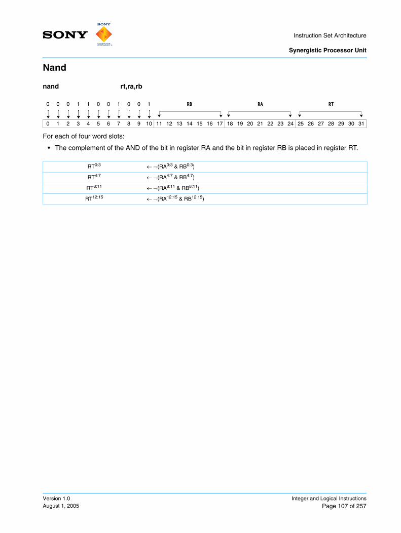
Instruction Set Architecture
Synergistic Processor Unit
Version 1.0August 1, 2005
Integer and Logical Instructions
Page 107 of 257
Nand
For each of four word slots:
• The complement of the AND of the bit in register RA and the bit in register RB is placed in register RT.
nand rt,ra,rb
0 0 0 1 1 0 0 1 0 0 1 RB RA RT
0 1 2 3 4 5 6 7 8 9 10 11 12 13 14 15 16 17 18 19 20 21 22 23 24 25 26 27 28 29 30 31
RT0:3 ← ¬(RA0:3 & RB0:3)
RT4:7 ← ¬(RA4:7 & RB4:7)
RT8:11 ← ¬(RA8:11 & RB8:11)
RT12:15 ← ¬(RA12:15 & RB12:15)

Instruction Set Architecture Synergistic Processor Unit
Integer and Logical Instructions
Page 108 of 257Version 1.0
August 1, 2005
Nor
For each of four word slots:
• The values in register RA and register RB are logically ORed.
• The result is complemented and placed in register RT.
nor rt,ra,rb
0 0 0 0 1 0 0 1 0 0 1 RB RA RT
0 1 2 3 4 5 6 7 8 9 10 11 12 13 14 15 16 17 18 19 20 21 22 23 24 25 26 27 28 29 30 31
RT0:3 ← ¬(RA0:3 | RB0:3)
RT4:7 ← ¬(RA4:7 | RB4:7)
RT8:11 ← ¬(RA8:11 | RB8:11)
RT12:15 ← ¬(RA12:15 | RB12:15)

Instruction Set Architecture
Synergistic Processor Unit
Version 1.0August 1, 2005
Integer and Logical Instructions
Page 109 of 257
Equivalent
For each of four word slots:
• If the bit in register RA and register RB are the same, the result is ‘1’; otherwise, the result is ‘0’.
• The result is placed in register RT.
eqv rt,ra,rb
0 1 0 0 1 0 0 1 0 0 1 RB RA RT
0 1 2 3 4 5 6 7 8 9 10 11 12 13 14 15 16 17 18 19 20 21 22 23 24 25 26 27 28 29 30 31
RT0:3 ← RA0:3 ⊕ (¬RB0:3)
RT4:7 ← RA4:7 ⊕ (¬RB4:7)
RT8:11 ← RA8:11 ⊕ (¬RB8:11)
RT12:15 ← RA12:15 ⊕ (¬RB12:15)

Instruction Set Architecture Synergistic Processor Unit
Integer and Logical Instructions
Page 110 of 257Version 1.0
August 1, 2005
Select Bits
For each of four word slots:
• If the bit in register RC is ‘0’, then select the bit from register RA; otherwise, select the bit from register RB.
• The selected bits are placed in register RT.
selb rt,ra,rb,rc
1 0 0 0 RT RB RA RC
0 1 2 3 4 5 6 7 8 9 10 11 12 13 14 15 16 17 18 19 20 21 22 23 24 25 26 27 28 29 30 31
RT0:15 ← RC0:15 & RB0:15 | (¬RC0:15) & RA0:15

Instruction Set Architecture
Synergistic Processor Unit
Version 1.0August 1, 2005
Integer and Logical Instructions
Page 111 of 257
Shuffle Bytes
Registers RA and RB are logically concatenated with the least-significant bit of RA adjacent to the most-significant bit of RB. The bytes of the resulting value are considered to be numbered from 0 to 31.
For each byte slot in registers RC and RT:
• The value in register RC is examined, and a result byte is produced as shown in Table 5-1.
• The result byte is inserted into register RT.
shufb rt,ra,rb,rc
1 0 1 1 RT RB RA RC
0 1 2 3 4 5 6 7 8 9 10 11 12 13 14 15 16 17 18 19 20 21 22 23 24 25 26 27 28 29 30 31
Table 5-1. Binary Values in Register RC and Byte Results
Value in Register RC(Expressed in Binary) Result Byte
10xxxxxx x‘00’
110xxxxx x‘FF’
111xxxxx x‘80’
Otherwise The byte of the concatenated register addressed by the rightmost 5 bits of register RC
Rconcat ← RA || RBFor j = 0 to 15
b ← RCj
If b0:1 = 0b10 then c ← 0x00; elseIf b0:2 = 0b110 then c ← 0xFF; elseIf b0:2 = 0b111 then c ← 0x80; else
Do; b ← b & 0x1F; c ← Rconcatb;
EndRTj ← c
End

Instruction Set Architecture Synergistic Processor Unit
Shift and Rotate Instructions
Page 112 of 257Version 1.0
August 1, 2005
6. Shift and Rotate Instructions
This section describes the SPU shift and rotate instructions.

Instruction Set Architecture
Synergistic Processor Unit
Version 1.0August 1, 2005
Shift and Rotate Instructions
Page 113 of 257
Shift Left Halfword
For each of eight halfword slots:
• The contents of register RA are shifted to the left according to the count in bits 11 to 15 of register RB.
• The result is placed in register RT.
• If the count is zero, the contents of register RA are copied unchanged into register RT. If the count is greater than 15, the result is zero.
• Bits shifted out of the left end of the halfword are discarded; zeros are shifted in at the right.
Note: Each halfword slot has its own independent shift amount.
shlh rt,ra,rb
0 0 0 0 1 0 1 1 1 1 1 RB RA RT
0 1 2 3 4 5 6 7 8 9 10 11 12 13 14 15 16 17 18 19 20 21 22 23 24 25 26 27 28 29 30 31
For j = 0 to 15 by 2s ← RBj::2 & 0x001Ft ← RAj::2
for b = 0 to 15if b + s < 16 then rb ← tb + selse rb ← 0
endRTj::2 ← r
end

Instruction Set Architecture Synergistic Processor Unit
Shift and Rotate Instructions
Page 114 of 257Version 1.0
August 1, 2005
Shift Left Halfword Immediate
For each of eight halfword slots:
• The contents of register RA are shifted to the left according to the count in bits 13 to 17 of the I7 field.
• The result is placed in register RT.
• If the count is zero, the contents of register RA are copied unchanged into register RT. If the count is greater than 15, the result is zero.
• Bits shifted out of the left end of the halfword are discarded; zeros are shifted in at the right.
shlhi rt,ra,value
0 0 0 0 1 1 1 1 1 1 1 I7 RA RT
0 1 2 3 4 5 6 7 8 9 10 11 12 13 14 15 16 17 18 19 20 21 22 23 24 25 26 27 28 29 30 31
s ← RepLeftBit(I7,16) & 0x001FFor j = 0 to 15 by 2
t ← RAj::2
for b = 0 to 15if b + s < 16 then rb ← tb + selse rb ← 0
endRTj::2 ← r
end

Instruction Set Architecture
Synergistic Processor Unit
Version 1.0August 1, 2005
Shift and Rotate Instructions
Page 115 of 257
Shift Left Word
For each of four word slots:
• The contents of register RA are shifted to the left according to the count in bits 26 to 31 of register RB.
• The result is placed in register RT.
• If the count is zero, the contents of register RA are copied unchanged into register RT. If the count is greater than 31, the result is zero.
• Bits shifted out of the left end of the word are discarded; zeros are shifted in at the right.
Note: Each word slot has its own independent shift amount.
shl rt,ra,rb
0 0 0 0 1 0 1 1 0 1 1 RB RA RT
0 1 2 3 4 5 6 7 8 9 10 11 12 13 14 15 16 17 18 19 20 21 22 23 24 25 26 27 28 29 30 31
For j = 0 to 15 by 4s ← RBj::4 & 0x0000003Ft ← RAj::4
for b = 0 to 31if b + s < 32 then rb ← tb + selse rb ← 0
endRTj::4 ← r
end

Instruction Set Architecture Synergistic Processor Unit
Shift and Rotate Instructions
Page 116 of 257Version 1.0
August 1, 2005
Shift Left Word Immediate
For each of four word slots:
• The contents of register RA are shifted to the left according to the count in bits 12 to 17 of the I7 field.
• The result is placed in register RT.
• If the count is zero, the contents of register RA are copied unchanged into register RT. If the count is greater than 31, the result is zero.
• Bits shifted out of the left end of the word are discarded; zeros are shifted in at the right.
shli rt,ra,value
0 0 0 0 1 1 1 1 0 1 1 I7 RA RT
0 1 2 3 4 5 6 7 8 9 10 11 12 13 14 15 16 17 18 19 20 21 22 23 24 25 26 27 28 29 30 31
s ← RepLeftBit(I7,32) & 0x0000003FFor j = 0 to 15 by 4
t ← RAj::4
for b = 0 to 31if b + s < 32 then rb ← tb + selse rb ← 0
endRTj::4 ← r
end

Instruction Set Architecture
Synergistic Processor Unit
Version 1.0August 1, 2005
Shift and Rotate Instructions
Page 117 of 257
Shift Left Quadword by Bits
The contents of register RA are shifted to the left according to the count in bits 29 to 31 of the preferred slot of register RB. The result is placed in register RT. A shift of up to 7 bit positions is possible.
If the count is zero, the contents of register RA are copied unchanged into register RT.
Bits shifted out of the left end of the register are discarded, and zeros are shifted in at the right.
shlqbi rt,ra,rb
0 0 1 1 1 0 1 1 0 1 1 RB RA RT
0 1 2 3 4 5 6 7 8 9 10 11 12 13 14 15 16 17 18 19 20 21 22 23 24 25 26 27 28 29 30 31
s ← RB29:31for b = 0 to 127
if b + s < 128 then rb ← RAb + selse rb ← 0
endRT ← r

Instruction Set Architecture Synergistic Processor Unit
Shift and Rotate Instructions
Page 118 of 257Version 1.0
August 1, 2005
Shift Left Quadword by Bits Immediate
The contents of register RA are shifted to the left according to the count in bits 15 to 17 of the I7 field. The result is placed in register RT. A shift of up to 7 bit positions is possible.
If the count is zero, the contents of register RA are copied unchanged into register RT.
Bits shifted out of the left end of the register are discarded, and zeros are shifted in at the right.
shlqbii rt,ra,value
0 0 1 1 1 1 1 1 0 1 1 I7 RA RT
0 1 2 3 4 5 6 7 8 9 10 11 12 13 14 15 16 17 18 19 20 21 22 23 24 25 26 27 28 29 30 31
s ← I7 & 0x07for b = 0 to 127
if b + s < 128 then rb ← RAb + selse rb ← 0
endRT ← r

Instruction Set Architecture
Synergistic Processor Unit
Version 1.0August 1, 2005
Shift and Rotate Instructions
Page 119 of 257
Shift Left Quadword by Bytes
The bytes of register RA are shifted to the left according to the count in bits 27 to 31 of the preferred slot of register RB. The result is placed in register RT.
If the count is zero, the contents of register RA are copied unchanged into register RT. If the count is greater than 15, the result is zero.
Bytes shifted out of the left end of the register are discarded, and bytes of zeros are shifted in at the right.
shlqby rt,ra,rb
0 0 1 1 1 0 1 1 1 1 1 RB RA RT
0 1 2 3 4 5 6 7 8 9 10 11 12 13 14 15 16 17 18 19 20 21 22 23 24 25 26 27 28 29 30 31
s ← RB27:31for b = 0 to 15
if b + s < 16 then rb ← RAb + s
else rb ← 0endRT ← r

Instruction Set Architecture Synergistic Processor Unit
Shift and Rotate Instructions
Page 120 of 257Version 1.0
August 1, 2005
Shift Left Quadword by Bytes Immediate
The bytes of register RA are shifted to the left according to the count in bits 13 to 17 of the I7 field. The result is placed in register RT.
If the count is zero, the contents of register RA are copied unchanged into register RT. If the count is greater than 15, the result is zero.
Bytes shifted out of the left end of the register are discarded, and zero bytes are shifted in at the right.
shlqbyi rt,ra,value
0 0 1 1 1 1 1 1 1 1 1 I7 RA RT
0 1 2 3 4 5 6 7 8 9 10 11 12 13 14 15 16 17 18 19 20 21 22 23 24 25 26 27 28 29 30 31
s ← I7 & 0x1Ffor b = 0 to 15
if b + s < 16 then rb ← RAb + s
else rb ← 0endRT ← r

Instruction Set Architecture
Synergistic Processor Unit
Version 1.0August 1, 2005
Shift and Rotate Instructions
Page 121 of 257
Shift Left Quadword by Bytes from Bit Shift Count
The bytes of register RA are shifted to the left according to the count in bits 24 to 28 of the preferred slot of register RB. The result is placed in register RT.
If the count is zero, the contents of register RA are copied unchanged into register RT. If the count is greater than 15, the result is zero.
Bytes shifted out of the left end of the register are discarded, and bytes of zeros are shifted in at the right.
shlqbybi rt,ra,rb
0 0 1 1 1 0 0 1 1 1 1 RB RA RT
0 1 2 3 4 5 6 7 8 9 10 11 12 13 14 15 16 17 18 19 20 21 22 23 24 25 26 27 28 29 30 31
s ← RB24:28for b = 0 to 15
if b + s < 16 then rb ← RAb + s
else rb ← x00endRT ← r

Instruction Set Architecture Synergistic Processor Unit
Shift and Rotate Instructions
Page 122 of 257Version 1.0
August 1, 2005
Rotate Halfword
For each of eight halfword slots:
• The contents of register RA are rotated to the left according to the count in bits 12 to 15 of register RB.
• The result is placed in register RT.
• If the count is zero, the contents of register RA are copied unchanged into register RT.
• Bits rotated out of the left end of the halfword are rotated in at the right end.
Note: Each halfword slot has its own independent rotate amount.
roth rt,ra,rb
0 0 0 0 1 0 1 1 1 0 0 RB RA RT
0 1 2 3 4 5 6 7 8 9 10 11 12 13 14 15 16 17 18 19 20 21 22 23 24 25 26 27 28 29 30 31
For j = 0 to 15 by 2s ← RBj::2 & 0x000Ft ← RAj::2
for b = 0 to 15if b + s < 16 then rb ← tb + selse rb ← tb + s - 16
endRTj::2 ← r
end

Instruction Set Architecture
Synergistic Processor Unit
Version 1.0August 1, 2005
Shift and Rotate Instructions
Page 123 of 257
Rotate Halfword Immediate
For each of eight halfword slots:
• The contents of register RA are rotated to the left according to the count in bits 14 to 17 of the I7 field.
• The result is placed in register RT.
• If the count is zero, the contents of register RA are copied unchanged into register RT.
• Bits rotated out of the left end of the halfword are rotated in at the right end.
rothi rt,ra,value
0 0 0 0 1 1 1 1 1 0 0 I7 RA RT
0 1 2 3 4 5 6 7 8 9 10 11 12 13 14 15 16 17 18 19 20 21 22 23 24 25 26 27 28 29 30 31
s ← RepLeftBit(I7,16) & 0x000FFor j = 0 to 15 by 2
t ← RAj::2
for b = 0 to 15if b + s < 16 then rb ← tb + selse rb ← tb + s - 16
endRTj::2 ← r
end

Instruction Set Architecture Synergistic Processor Unit
Shift and Rotate Instructions
Page 124 of 257Version 1.0
August 1, 2005
Rotate Word
For each of four word slots:
• The contents of register RA are rotated to the left according to the count in bits 27 to 31 of register RB.
• The result is placed in register RT.
• If the count is zero, the contents of register RA are copied unchanged into register RT.
• Bits rotated out of the left end of the word are rotated in at the right end.
rot rt,ra,rb
0 0 0 0 1 0 1 1 0 0 0 RB RA RT
0 1 2 3 4 5 6 7 8 9 10 11 12 13 14 15 16 17 18 19 20 21 22 23 24 25 26 27 28 29 30 31
For j = 0 to 15 by 4s ← RBj::4 & 0x0000001Ft ← RAj::4
for b = 0 to 31if b + s < 32 then rb ← tb + selse rb ← tb + s - 32
endRTj::4 ← r
end

Instruction Set Architecture
Synergistic Processor Unit
Version 1.0August 1, 2005
Shift and Rotate Instructions
Page 125 of 257
Rotate Word Immediate
For each of four word slots:
• The contents of register RA are rotated to the left according to the count in bits 13 to 17 of the I7 field.
• The result is placed in register RT.
• If the count is zero, the contents of register RA are copied unchanged into register RT.
• Bits rotated out of the left end of the word are rotated in at the right end.
roti rt,ra,value
0 0 0 0 1 1 1 1 0 0 0 I7 RA RT
0 1 2 3 4 5 6 7 8 9 10 11 12 13 14 15 16 17 18 19 20 21 22 23 24 25 26 27 28 29 30 31
s ← RepLeftBit(I7,32) & 0x0000001FFor j = 0 to 15 by 4
t ← RAj::4
for b = 0 to 31if b + s < 32 then rb ← tb + selse rb ← tb + s - 32
endRTj::4 ← r
end

Instruction Set Architecture Synergistic Processor Unit
Shift and Rotate Instructions
Page 126 of 257Version 1.0
August 1, 2005
Rotate Quadword by Bytes
The bytes in register RA are rotated to the left according to the count in the rightmost 4 bits of the preferred slot of register RB. The result is placed in register RT. Rotation of up to 15 byte positions is possible.
If the count is zero, the contents of register RA are copied unchanged into register RT.
Bytes rotated out of the left end of the register are rotated in at the right.
rotqby rt,ra,rb
0 0 1 1 1 0 1 1 1 0 0 RB RA RT
0 1 2 3 4 5 6 7 8 9 10 11 12 13 14 15 16 17 18 19 20 21 22 23 24 25 26 27 28 29 30 31
t4 ← RB28:31If t4 = 0 then r ← RA; Else Do
For i = 0 to 15c = mod(i + t4,16)ri ← RAc
EndEndRT ← r

Instruction Set Architecture
Synergistic Processor Unit
Version 1.0August 1, 2005
Shift and Rotate Instructions
Page 127 of 257
Rotate Quadword by Bytes Immediate
The bytes in register RA are rotated to the left according to the count in the rightmost 4 bits of the I7 field. The result is placed in register RT. Rotation of up to 15 byte positions is possible.
If the count is zero, the contents of register RA are copied unchanged into register RT.
Bytes rotated out of the left end of the register are rotated in at the right.
rotqbyi rt,ra,value
0 0 1 1 1 1 1 1 1 0 0 I7 RA RT
0 1 2 3 4 5 6 7 8 9 10 11 12 13 14 15 16 17 18 19 20 21 22 23 24 25 26 27 28 29 30 31
t4 ← I714:17If t4 = 0 then r ← RA;
Else DoFor i = 0 to 15
c = mod(i + t4,16)ri ← RAc
EndEndRT ← r

Instruction Set Architecture Synergistic Processor Unit
Shift and Rotate Instructions
Page 128 of 257Version 1.0
August 1, 2005
Rotate Quadword by Bytes from Bit Shift Count
The bytes of register RA are rotated to the left according to the count in bits 25 to 28 of the preferred slot of register RB. The result is placed in register RT.
If the count is zero, the contents of register RA are copied unchanged into register RT.
Bytes rotated out of the left end of the register are rotated in at the right.
rotqbybi rt,ra,rb
0 0 1 1 1 0 0 1 1 0 0 RB RA RT
0 1 2 3 4 5 6 7 8 9 10 11 12 13 14 15 16 17 18 19 20 21 22 23 24 25 26 27 28 29 30 31
s ← RB24:28for b = 0 to 15
if b + s < 16 then rb ← RAb + s
else rb ← RAb + s - 16
endRT ← r

Instruction Set Architecture
Synergistic Processor Unit
Version 1.0August 1, 2005
Shift and Rotate Instructions
Page 129 of 257
Rotate Quadword by Bits
The contents of register RA are rotated to the left according to the count in bits 29 to 31 of the preferred slot of register RB. The result is placed in register RT. Rotation of up to 7 bit positions is possible.
If the count is zero, the contents of register RA are copied unchanged into register RT.
Bits rotated out at the left end of the register are rotated in at the right.
rotqbi rt,ra,rb
0 0 1 1 1 0 1 1 0 0 0 RB RA RT
0 1 2 3 4 5 6 7 8 9 10 11 12 13 14 15 16 17 18 19 20 21 22 23 24 25 26 27 28 29 30 31
s ← RB29:31for b = 0 to 127
if b + s < 128 then rb ← RAb + selse rb ← RAb + s - 128
endRT ← r

Instruction Set Architecture Synergistic Processor Unit
Shift and Rotate Instructions
Page 130 of 257Version 1.0
August 1, 2005
Rotate Quadword by Bits Immediate
The contents of register RA are rotated to the left according to the count in bits 15 to 17 of the I7 field. The result is placed in register RT. Rotation of up to 7 bit positions is possible.
If the count is zero, the contents of register RA are copied unchanged into register RT.
Bits rotated out at the left end of the register are rotated in at the right.
rotqbii rt,ra,value
0 0 1 1 1 1 1 1 0 0 0 I7 RA RT
0 1 2 3 4 5 6 7 8 9 10 11 12 13 14 15 16 17 18 19 20 21 22 23 24 25 26 27 28 29 30 31
s ← I4:6for b = 0 to 127
if b + s < 128 then rb ← RAb + selse rb ← RAb + s - 128
endRT ← r

Instruction Set Architecture
Synergistic Processor Unit
Version 1.0August 1, 2005
Shift and Rotate Instructions
Page 131 of 257
Rotate and Mask Halfword
For each of eight halfword slots:
• The shift_count is (0 - RB) modulo 32.
• If the shift_count is less than 16, then RT is set to the contents of RA shifted right shift_count bits, with zero fill at the left.
• Otherwise, RT is set to zero.
Note: Each halfword slot has its own independent rotate amount.
Programming Note: The Rotate and Mask and Rotate and Mask Algebraic instructions provide support for a logical right shift and algebraic right shift, respectively. They differ from a conventional right logical or alge-braic shift in that the shift amount accepted by the instructions is the twos complement of the right shift amount. Thus, to shift right logically the contents of R2 by the number of bits given in R1, the following sequence could be used:
For the immediate forms of these instructions, the formation of the twos complement shift quantity can be performed during assembly or compilation.
rothm rt,ra,rb
0 0 0 0 1 0 1 1 1 0 1 RB RA RT
0 1 2 3 4 5 6 7 8 9 10 11 12 13 14 15 16 17 18 19 20 21 22 23 24 25 26 27 28 29 30 31
For j = 0 to 15 by 2s ← (0 - RBj::2) & 0x001Ft ← RAj::2
for b = 0 to 15if b ≥ s then rb ← tb - selse rb ← 0
endRTj::2 ← r
end
sfi r3,r1,0 Form twos complement rotm r4,r2,r3 Rotate, then mask

Instruction Set Architecture Synergistic Processor Unit
Shift and Rotate Instructions
Page 132 of 257Version 1.0
August 1, 2005
Rotate and Mask Halfword Immediate
For each of eight halfword slots:
• The shift_count is (0 - I7) modulo 32.
• If the shift_count is less than 16, then RT is set to the contents of RA shifted right shift_count bits, with zero fill at the left.
• Otherwise, RT is set to zero.
Programming Note: The Rotate and Mask and Rotate and Mask Algebraic instructions provide support for a logical right shift and algebraic right shift, respectively. They differ from a conventional right logical or alge-braic shift in that the shift amount accepted by the instructions is the twos complement of the right shift amount. Thus, to shift right logically the contents of R2 by the number of bits given in R1, the following sequence could be used:
For the immediate forms of these instructions, the formation of the twos complement shift quantity can be performed during assembly or compilation.
rothmi rt,ra,value
0 0 0 0 1 1 1 1 1 0 1 I7 RA RT
0 1 2 3 4 5 6 7 8 9 10 11 12 13 14 15 16 17 18 19 20 21 22 23 24 25 26 27 28 29 30 31
s ← (0 - RepLeftBit(I7,32)) & 0x0000003FFor j = 0 to 15 by 4
t ← RAj::4
for b = 0 to 31if b ≥ s then rb ← tb - selse rb ← t0
endRTj::4 ← r
end
sfi r3,r1,0 Form twos complement rotm r4,r2,r3 Rotate, then mask

Instruction Set Architecture
Synergistic Processor Unit
Version 1.0August 1, 2005
Shift and Rotate Instructions
Page 133 of 257
Rotate and Mask Word
For each of four word slots:
• The shift_count is (0 - RB) modulo 64.
• If the shift_count is less than 32, then RT is set to the contents of RA shifted right shift_count bits, with zero fill at the left.
• Otherwise, RT is set to zero.
Programming Note: The Rotate and Mask and Rotate and Mask Algebraic instructions provide support for a logical right shift and algebraic right shift, respectively. They differ from a conventional right logical or alge-braic shift in that the shift amount accepted by the instructions is the twos complement of the right shift amount. Thus, to shift right logically the contents of R2 by the number of bits given in R1, the following sequence could be used:
For the immediate forms of these instructions, the formation of the twos complement shift quantity can be performed during assembly or compilation.
rotm rt,ra,rb
0 0 0 0 1 0 1 1 0 0 1 RB RA RT
0 1 2 3 4 5 6 7 8 9 10 11 12 13 14 15 16 17 18 19 20 21 22 23 24 25 26 27 28 29 30 31
For j = 0 to 15 by 4s ← (0 - RBj::4) & 0x0000003Ft ← RAj::4
for b = 0 to 31if b ≥ s then rb ← tb - selse rb ← 0
endRTj::4 ← r
end
sfi r3,r1,0 Form twos complementrotm r4,r2,r3 Rotate, then mask

Instruction Set Architecture Synergistic Processor Unit
Shift and Rotate Instructions
Page 134 of 257Version 1.0
August 1, 2005
Rotate and Mask Word Immediate
For each of four word slots:
• The shift_count is (0 - I7) modulo 64.
• If the shift_count is less than 32, then RT is set to the contents of RA shifted right shift_count bits, with zero fill at the left.
• Otherwise, RT is set to zero.
Programming Note: The Rotate and Mask and Rotate and Mask Algebraic instructions provide support for a logical right shift and algebraic right shift, respectively. They differ from a conventional right logical or alge-braic shift in that the shift amount accepted by the instructions is the twos complement of the right shift amount. Thus, to shift right logically the contents of R2 by the number of bits given in R1, the following sequence could be used.
For the immediate forms of these instructions, the formation of the twos complement shift quantity can be performed during assembly or compilation.
rotmi rt,ra,value
0 0 0 0 1 1 1 1 0 0 1 I7 RA RT
0 1 2 3 4 5 6 7 8 9 10 11 12 13 14 15 16 17 18 19 20 21 22 23 24 25 26 27 28 29 30 31
s ← (0 - RepLeftBit(I7,32)) & 0x0000003FFor j = 0 to 15 by 4
t ← RAj::4
for b = 0 to 31if b ≥ s then rb ← tb - selse rb ← 0
endRTj::4 ← r
end
sfi r3,r1,0 Form twos complementrotm r4,r2,r3 Rotate, then mask

Instruction Set Architecture
Synergistic Processor Unit
Version 1.0August 1, 2005
Shift and Rotate Instructions
Page 135 of 257
Rotate and Mask Quadword by Bytes
The shift_count is (0 - the preferred word of RB) modulo 32. If the shift_count is less than 16, then RT is set to the contents of RA shifted right shift_count bytes, filling at the left with x‘00’ bytes. Otherwise, RT is set to zero.
rotqmby rt,ra,rb
0 0 1 1 1 0 1 1 1 0 1 RB RA RT
0 1 2 3 4 5 6 7 8 9 10 11 12 13 14 15 16 17 18 19 20 21 22 23 24 25 26 27 28 29 30 31
s ← (0 - RB27:31) & 0x1Ffor b = 0 to 15
if b ≥ s then rb ← tb - s
else rb ← 0x00endRT ← r
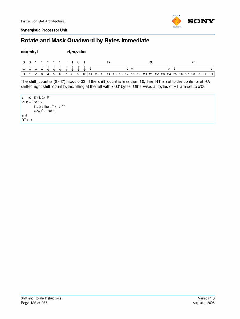
Instruction Set Architecture Synergistic Processor Unit
Shift and Rotate Instructions
Page 136 of 257Version 1.0
August 1, 2005
Rotate and Mask Quadword by Bytes Immediate
The shift_count is (0 - I7) modulo 32. If the shift_count is less than 16, then RT is set to the contents of RA shifted right shift_count bytes, filling at the left with x‘00’ bytes. Otherwise, all bytes of RT are set to x‘00’.
rotqmbyi rt,ra,value
0 0 1 1 1 1 1 1 1 0 1 I7 RA RT
0 1 2 3 4 5 6 7 8 9 10 11 12 13 14 15 16 17 18 19 20 21 22 23 24 25 26 27 28 29 30 31
s ← (0 - I7) & 0x1Ffor b = 0 to 15
if b ≥ s then rb ← tb - s
else rb ← 0x00endRT ← r

Instruction Set Architecture
Synergistic Processor Unit
Version 1.0August 1, 2005
Shift and Rotate Instructions
Page 137 of 257
Rotate and Mask Quadword Bytes from Bit Shift Count
The shift_count is (0 minus bits 24 to 28 of RB) modulo 32. If the shift_count is less than 16, then RT is set to the contents of RA, which is shifted right shift_count bytes, and filled at the left with x‘00’ bytes. Otherwise, all bytes of RT are set to x‘00’.
rotqmbybi rt,ra,rb
0 0 1 1 1 0 0 1 1 0 1 RB RA RT
0 1 2 3 4 5 6 7 8 9 10 11 12 13 14 15 16 17 18 19 20 21 22 23 24 25 26 27 28 29 30 31
s ← (0 - RB24:28) & 0x1Ffor b = 0 to 15
if b ≥ s then rb ← RAb - s
else rb ← 0x00end

Instruction Set Architecture Synergistic Processor Unit
Shift and Rotate Instructions
Page 138 of 257Version 1.0
August 1, 2005
Rotate and Mask Quadword by Bits
The shift_count is (0 - the preferred word of RB) modulo 8. RT is set to the contents of RA, shifted right by shift_count bits, filling at the left with zero bits.
rotqmbi rt,ra,rb
0 0 1 1 1 0 1 1 0 0 1 RB RA RT
0 1 2 3 4 5 6 7 8 9 10 11 12 13 14 15 16 17 18 19 20 21 22 23 24 25 26 27 28 29 30 31
s ← (0 - RB29:31) & 0x07for b = 0 to 127
if b ≥ s then rb ← tb - selse rb ← 0
endRT ← r

Instruction Set Architecture
Synergistic Processor Unit
Version 1.0August 1, 2005
Shift and Rotate Instructions
Page 139 of 257
Rotate and Mask Quadword by Bits Immediate
The shift_count is (0 - I7) modulo 8. RT is set to the contents of RA, shifted right by shift_count bits, filling at the left with zero bits.
rotqmbii rt,ra,value
0 0 1 1 1 1 1 1 0 0 1 I7 RA RT
0 1 2 3 4 5 6 7 8 9 10 11 12 13 14 15 16 17 18 19 20 21 22 23 24 25 26 27 28 29 30 31
s ← (0 - I7) & 0x07for b = 0 to 127
if b ≥ s then rb ← tb - selse rb ← 0
endRT ← r

Instruction Set Architecture Synergistic Processor Unit
Shift and Rotate Instructions
Page 140 of 257Version 1.0
August 1, 2005
Rotate and Mask Algebraic Halfword
For each of eight halfword slots:
• The shift_count is (0 - RB) modulo 32.
• If the shift_count is less than 16, then RT is set to the contents of RA shifted right shift_count bits, repli-cating bit 0 (of the halfword) at the left.
• Otherwise, all bits of this halfword of RT are set to bit 0 of this halfword of RA.
Note: Each halfword slot has its own independent rotate amount.
rotmah rt,ra,rb
0 0 0 0 1 0 1 1 1 1 0 RB RA RT
0 1 2 3 4 5 6 7 8 9 10 11 12 13 14 15 16 17 18 19 20 21 22 23 24 25 26 27 28 29 30 31
For j = 0 to 15 by 2s ← (0 - RBj::2) & 0x001Ft ← RAj::2
for b = 0 to 15if b ≥ s then rb ← tb - selse rb ← t0
endRTj::2 ← r
end

Instruction Set Architecture
Synergistic Processor Unit
Version 1.0August 1, 2005
Shift and Rotate Instructions
Page 141 of 257
Rotate and Mask Algebraic Halfword Immediate
For each of eight halfword slots:
• The shift_count is (0 - I7) modulo 32.
• If the shift_count is less than 16, then RT is set to the contents of RA shifted right shift_count bits, repli-cating bit 0 (of the halfword) at the left.
• Otherwise, all bits of this halfword of RT are set to bit 0 of this halfword of RA.
rotmahi rt,ra,value
0 0 0 0 1 1 1 1 1 1 0 I7 RA RT
0 1 2 3 4 5 6 7 8 9 10 11 12 13 14 15 16 17 18 19 20 21 22 23 24 25 26 27 28 29 30 31
s ← (0 - RepLeftBit(I7,16)) & 0x001FFor j = 0 to 15 by 2
t ← RAj::2
for b = 0 to 15if b ≥ s then rb ← tb - selse rb ← t0
endRTj::2 ← r
end

Instruction Set Architecture Synergistic Processor Unit
Shift and Rotate Instructions
Page 142 of 257Version 1.0
August 1, 2005
Rotate and Mask Algebraic Word
For each of four word slots:
• The shift_count is (0 - RB) modulo 64.
• If the shift_count is less than 32, then RT is set to the contents of RA shifted right shift_count bits, repli-cating bit 0 (of the word) at the left.
• Otherwise, all bits of this word of RT are set to bit 0 of this word of RA.
rotma rt,ra,rb
0 0 0 0 1 0 1 1 0 1 0 RB RA RT
0 1 2 3 4 5 6 7 8 9 10 11 12 13 14 15 16 17 18 19 20 21 22 23 24 25 26 27 28 29 30 31
For j = 0 to 15 by 4s ← (0 - RBj::4) & 0x0000003Ft ← RAj::4
for b = 0 to 31if b ≥ s then rb ← tb - selse rb ← t0
endRTj::4 ← r
end
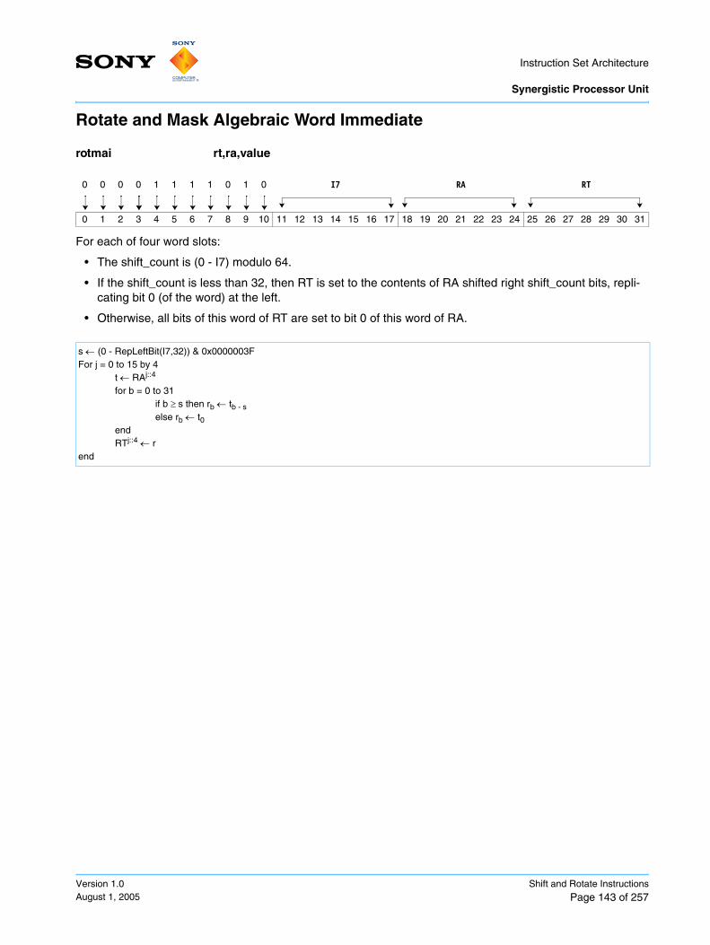
Instruction Set Architecture
Synergistic Processor Unit
Version 1.0August 1, 2005
Shift and Rotate Instructions
Page 143 of 257
Rotate and Mask Algebraic Word Immediate
For each of four word slots:
• The shift_count is (0 - I7) modulo 64.
• If the shift_count is less than 32, then RT is set to the contents of RA shifted right shift_count bits, repli-cating bit 0 (of the word) at the left.
• Otherwise, all bits of this word of RT are set to bit 0 of this word of RA.
rotmai rt,ra,value
0 0 0 0 1 1 1 1 0 1 0 I7 RA RT
0 1 2 3 4 5 6 7 8 9 10 11 12 13 14 15 16 17 18 19 20 21 22 23 24 25 26 27 28 29 30 31
s ← (0 - RepLeftBit(I7,32)) & 0x0000003FFor j = 0 to 15 by 4
t ← RAj::4
for b = 0 to 31if b ≥ s then rb ← tb - selse rb ← t0
endRTj::4 ← r
end

Instruction Set Architecture Synergistic Processor Unit
Compare, Branch, and Halt Instructions
Page 144 of 257Version 1.0
August 1, 2005
7. Compare, Branch, and Halt Instructions
This section lists and describes the SPU compare, branch, and halt instructions. For more information on the SPU interrupt facility, see Section 12 on page 238.
Conditional branch instructions operate by examining a value in a register, rather than by accessing a specialized condition code register. The value is taken from the preferred slot. It is usually set by a compare instruction.
Compare instructions perform a comparison of the values in two registers, or a value in a register and an immediate value. The result is indicated by setting into the target register a result value that is the same width as the register operands. If the comparison condition is met, the value is all one bits; if not, the value is all zero bits.
Logical comparison instructions treat the operands as unsigned integers. Other compare instructions treat the operands as twos complement signed integers.
A set of “Halt” instructions is provided that stops execution when the tested condition is met. These are intended to be used, for example, to check addresses or subscript ranges in situations where failure to meet the condition is regarded as a serious error. The stop that occurs is not precise, so execution can generally not be restarted.
Floating-point compare instructions are listed in Section 9 Floating-Point Instructions on page 189 with the other floating-point instructions.

Instruction Set Architecture
Synergistic Processor Unit
Version 1.0August 1, 2005
Compare, Branch, and Halt Instructions
Page 145 of 257
Halt If Equal
The value in the preferred slot of register RA is compared with the value in the preferred slot of register RB. If the values are equal, execution of the program stops at or after the halt.
Programming Note: RT is a false target. Implementations can schedule instructions as though this instruc-tion produces a value into RT. Programs can avoid unnecessary delay by programming RT so as not to appear to source data for nearby subsequent instructions. False targets are not written..
heq ra,rb
0 1 1 1 1 0 1 1 0 0 0 RB RA RT
0 1 2 3 4 5 6 7 8 9 10 11 12 13 14 15 16 17 18 19 20 21 22 23 24 25 26 27 28 29 30 31
If RA0:3 = RB0:3 thenStop after executing zero or more instructions after the halt.
End

Instruction Set Architecture Synergistic Processor Unit
Compare, Branch, and Halt Instructions
Page 146 of 257Version 1.0
August 1, 2005
Halt If Equal Immediate
The value in the I10 field is extended to 32 bits by replicating the leftmost bit. The result is algebraically compared to the value in the preferred slot of register RA. If the value from register RA is equal to the imme-diate value, execution of the SPU program stops at or after the halt instruction.
Programming Note: RT is a false target. Implementations can schedule instructions as though this instruc-tion produces a value into RT. Programs can avoid unnecessary delay by programming RT so as not to appear to source data for nearby subsequent instructions. False targets are not written.
heqi ra,symbol
0 1 1 1 1 1 1 1 I10 RA RT
0 1 2 3 4 5 6 7 8 9 10 11 12 13 14 15 16 17 18 19 20 21 22 23 24 25 26 27 28 29 30 31
If RA0:3 = RepLeftBit(I10,32) thenStop after executing zero or more instructions after the halt.
End

Instruction Set Architecture
Synergistic Processor Unit
Version 1.0August 1, 2005
Compare, Branch, and Halt Instructions
Page 147 of 257
Halt If Greater Than
The value in the preferred slot of register RA is compared with the value in the preferred slot of register RB. If the value from register RA is greater than the RB value, execution of the SPU program stops at or after the halt instruction.
Programming Note: RT is a false target. Implementations can schedule instructions as though this instruc-tion produces a value into RT. Programs can avoid unnecessary delay by programming RT so as not to appear to source data for nearby subsequent instructions. False targets are not written.
hgt ra,rb
0 1 0 0 1 0 1 1 0 0 0 RB RA RT
0 1 2 3 4 5 6 7 8 9 10 11 12 13 14 15 16 17 18 19 20 21 22 23 24 25 26 27 28 29 30 31
If RA0:3 > RB0:3 thenStop after executing zero or more instructions after the halt.
End

Instruction Set Architecture Synergistic Processor Unit
Compare, Branch, and Halt Instructions
Page 148 of 257Version 1.0
August 1, 2005
Halt If Greater Than Immediate
The value in the I10 field is extended to 32 bits by replicating the leftmost bit. The result is algebraically compared to the value in the preferred slot of register RA. If the value from register RA is greater than the immediate value, execution of the SPU program stops at or after the halt instruction.
Programming Note: RT is a false target. Implementations can schedule instructions as though this instruc-tion produces a value into RT. Programs can avoid unnecessary delay by programming RT so as not to appear to source data for nearby subsequent instructions. False targets are not written.
hgti ra,symbol
0 1 0 0 1 1 1 1 I10 RA RT
0 1 2 3 4 5 6 7 8 9 10 11 12 13 14 15 16 17 18 19 20 21 22 23 24 25 26 27 28 29 30 31
If RA0:3 > RepLeftBit(I10,32) thenStop after executing zero or more instructions after the halt.
End

Instruction Set Architecture
Synergistic Processor Unit
Version 1.0August 1, 2005
Compare, Branch, and Halt Instructions
Page 149 of 257
Halt If Logically Greater Than
The value in the preferred slot of register RA is compared with the value in the preferred slot of register RB. If the value from register RA is greater than the value from register RB, execution of the SPU program stops at or after the halt instruction.
Programming Note: RT is a false target. Implementations can schedule instructions as though this instruc-tion produces a value into RT. Programs can avoid unnecessary delay by programming RT so as not to appear to source data for nearby subsequent instructions. False targets are not written.
hlgt ra,rb
0 1 0 1 1 0 1 1 0 0 0 RB RA RT
0 1 2 3 4 5 6 7 8 9 10 11 12 13 14 15 16 17 18 19 20 21 22 23 24 25 26 27 28 29 30 31
If RA0:3 >u RB0:3 thenStop after executing zero or more instructions after the halt.
End

Instruction Set Architecture Synergistic Processor Unit
Compare, Branch, and Halt Instructions
Page 150 of 257Version 1.0
August 1, 2005
Halt If Logically Greater Than Immediate
The value in the I10 field is extended to 32 bits by replicating the leftmost bit. The result is logically compared to the value in the preferred slot of register RA. If the value from register RA is logically greater than the immediate value, execution of the SPU program stops at or after the halt instruction.
Programming Note: RT is a false target. Implementations can schedule instructions as though this instruc-tion produces a value into RT. Programs can avoid unnecessary delay by programming RT so as not to appear to source data for nearby subsequent instructions. False targets are not written.
hlgti ra,symbol
0 1 0 1 1 1 1 1 I10 RA RT
0 1 2 3 4 5 6 7 8 9 10 11 12 13 14 15 16 17 18 19 20 21 22 23 24 25 26 27 28 29 30 31
If RA0:3 >u RepLeftBit(I10,32) thenStop after executing zero or more instructions after the halt.
End

Instruction Set Architecture
Synergistic Processor Unit
Version 1.0August 1, 2005
Compare, Branch, and Halt Instructions
Page 151 of 257
Compare Equal Byte
For each of 16 byte slots:
• The operand from register RA is compared with the operand from register RB. If the operands are equal, a result of all one bits (true) is produced. If they are unequal, a result of all zero bits (false) is produced.
• The 8-bit result is placed in register RT.
ceqb rt,ra,rb
0 1 1 1 1 0 1 0 0 0 0 RB RA RT
0 1 2 3 4 5 6 7 8 9 10 11 12 13 14 15 16 17 18 19 20 21 22 23 24 25 26 27 28 29 30 31
for i = 0 to 15If RAi = RBi then
RTi ← 0xFFelse
RTi ← 0x00End

Instruction Set Architecture Synergistic Processor Unit
Compare, Branch, and Halt Instructions
Page 152 of 257Version 1.0
August 1, 2005
Compare Equal Byte Immediate
For each of 16 byte slots:
• The value in the rightmost 8 bits of the I10 field is compared with the value in register RA. If the two val-ues are equal, a result of all one bits (true) is produced. If they are unequal, a result of all zero bits (false) is produced.
• The 8-bit result is placed in register RT.
ceqbi rt,ra,value
0 1 1 1 1 1 1 0 I10 RA RT
0 1 2 3 4 5 6 7 8 9 10 11 12 13 14 15 16 17 18 19 20 21 22 23 24 25 26 27 28 29 30 31
for i = 0 to 15If RAi = I102:9 then
RTi ← 0xFFelse
RTi ← 0x00End

Instruction Set Architecture
Synergistic Processor Unit
Version 1.0August 1, 2005
Compare, Branch, and Halt Instructions
Page 153 of 257
Compare Equal Halfword
For each of 8 halfword slots:
• The operand from register RA is compared with the operand from register RB. If the operands are equal, a result of all one bits (true) is produced. If they are unequal, a result of all zero bits (false) is produced.
• The 16-bit result is placed in register RT.
ceqh rt,ra,rb
0 1 1 1 1 0 0 1 0 0 0 RB RA RT
0 1 2 3 4 5 6 7 8 9 10 11 12 13 14 15 16 17 18 19 20 21 22 23 24 25 26 27 28 29 30 31
for i = 0 to 15 by 2If RAi::2 = RBi::2 then
RTi::2 ← 0xFFFFelse
RTi::2 ← 0x0000End

Instruction Set Architecture Synergistic Processor Unit
Compare, Branch, and Halt Instructions
Page 154 of 257Version 1.0
August 1, 2005
Compare Equal Halfword Immediate
For each of eight halfword slots:
• The value in the I10 field is extended to 16 bits by replicating its leftmost bit and compared with the value in register RA. If the two values are equal, a result of all one bits (true) is produced. If they are unequal, a result of all zero bits (false) is produced.
• The 16-bit result is placed in register RT.
ceqhi rt,ra,value
0 1 1 1 1 1 0 1 I10 RA RT
0 1 2 3 4 5 6 7 8 9 10 11 12 13 14 15 16 17 18 19 20 21 22 23 24 25 26 27 28 29 30 31
for i = 0 to 15 by 2If RAi::2 = RepLeftBit(I10,16) then
RTi::2 ← 0xFFFFelse
RTi::2 ← 0x0000End

Instruction Set Architecture
Synergistic Processor Unit
Version 1.0August 1, 2005
Compare, Branch, and Halt Instructions
Page 155 of 257
Compare Equal Word
For each of four word slots:
• The operand from register RA is compared with the operand from register RB. If the operands are equal, a result of all one bits (true) is produced. If they are unequal, a result of all zero bits (false) is produced.
• The 32-bit result is placed in register RT.
ceq rt,ra,rb
0 1 1 1 1 0 0 0 0 0 0 RB RA RT
0 1 2 3 4 5 6 7 8 9 10 11 12 13 14 15 16 17 18 19 20 21 22 23 24 25 26 27 28 29 30 31
for i = 0 to 15 by 4If RAi::4 = RBi::4 then
RTi::4 ← 0xFFFFFFFFelse
RTi::4 ← 0x00000000End

Instruction Set Architecture Synergistic Processor Unit
Compare, Branch, and Halt Instructions
Page 156 of 257Version 1.0
August 1, 2005
Compare Equal Word Immediate
For each of four word slots:
• The I10 field is extended to 32 bits by replicating its leftmost bit and comparing it with the value in register RA. If the two values are equal, a result of all one bits (true) is produced. If they are unequal, a result of all zero bits (false) is produced.
• The 32-bit result is placed in register RT.
ceqi rt,ra,value
0 1 1 1 1 1 0 0 I10 RA RT
0 1 2 3 4 5 6 7 8 9 10 11 12 13 14 15 16 17 18 19 20 21 22 23 24 25 26 27 28 29 30 31
for i = 0 to 15 by 4If RAi::4 = RepLeftBit(I10,32) then
RTi::4 ← 0xFFFFFFFFelse
RTi::4 ← 0x00000000End

Instruction Set Architecture
Synergistic Processor Unit
Version 1.0August 1, 2005
Compare, Branch, and Halt Instructions
Page 157 of 257
Compare Greater Than Byte
For each of 16 byte slots:
• The operand from register RA is compared with the operand from register RB. If the operand in register RA is greater than the operand in register RB, a result of all one bits (true) is produced. Otherwise, a result of all zero bits (false) is produced.
• The 8-bit result is placed in register RT.
cgtb rt,ra,rb
0 1 0 0 1 0 1 0 0 0 0 RB RA RT
0 1 2 3 4 5 6 7 8 9 10 11 12 13 14 15 16 17 18 19 20 21 22 23 24 25 26 27 28 29 30 31
for i = 0 to 15If RAi > RBi then
RTi ← 0xFFelse
RTi ← 0x00End

Instruction Set Architecture Synergistic Processor Unit
Compare, Branch, and Halt Instructions
Page 158 of 257Version 1.0
August 1, 2005
Compare Greater Than Byte Immediate
For each of 16 byte slots:
• The value in the rightmost 8 bits of the I10 field is algebraically compared with the value in register RA. If the value in register RA is greater, a result of all one bits (true) is produced. Otherwise, a result of all zero bits (false) is produced.
• The 8-bit result is placed in register RT.
cgtbi rt,ra,value
0 1 0 0 1 1 1 0 I10 RA RT
0 1 2 3 4 5 6 7 8 9 10 11 12 13 14 15 16 17 18 19 20 21 22 23 24 25 26 27 28 29 30 31
for i = 0 to 15If RAi > I102:9 then
RTi ← 0xFFelse
RTi ← 0x00End

Instruction Set Architecture
Synergistic Processor Unit
Version 1.0August 1, 2005
Compare, Branch, and Halt Instructions
Page 159 of 257
Compare Greater Than Halfword
For each of 8 halfword slots:
• The operand from register RA is compared with the operand from register RB. If the operand in register RA is greater than the operand in register RB, a result of all one bits (true) is produced. Otherwise, a result of all zero bits (false) is produced.
• The 16-bit result is placed in register RT.
cgth rt,ra,rb
0 1 0 0 1 0 0 1 0 0 0 RB RA RT
0 1 2 3 4 5 6 7 8 9 10 11 12 13 14 15 16 17 18 19 20 21 22 23 24 25 26 27 28 29 30 31
for i = 0 to 15 by 2If RAi::2 > RBi::2 then
RTi::2 ← 0xFFFFelse
RTi::2 ← 0x0000End

Instruction Set Architecture Synergistic Processor Unit
Compare, Branch, and Halt Instructions
Page 160 of 257Version 1.0
August 1, 2005
Compare Greater Than Halfword Immediate
For each of eight halfword slots:
• The value in the I10 field is extended to 16 bits and algebraically compared with the value in register RA. If the value in register RA is greater than the I10 value, a result of all one bits (true) is produced. Other-wise, a result of all zero bits (false) is produced.
• The 16-bit result is placed in register RT.
cgthi rt,ra,value
0 1 0 0 1 1 0 1 I10 RA RT
0 1 2 3 4 5 6 7 8 9 10 11 12 13 14 15 16 17 18 19 20 21 22 23 24 25 26 27 28 29 30 31
for i = 0 to 15 by 2If RAi::2 > RepLeftBit(I10,16) then
RTi::2 ← 0xFFFFelse
RTi::2 ← 0x0000End

Instruction Set Architecture
Synergistic Processor Unit
Version 1.0August 1, 2005
Compare, Branch, and Halt Instructions
Page 161 of 257
Compare Greater Than Word
For each of four word slots:
• The operand from register RA is compared with the operand from register RB. If the operand in register RA is greater than the operand in register RB, a result of all one bits (true) is produced. Otherwise, a result of all zero bits (false) is produced.
• The 32-bit result is placed in register RT.
cgt rt,ra,rb
0 1 0 0 1 0 0 0 0 0 0 RB RA RT
0 1 2 3 4 5 6 7 8 9 10 11 12 13 14 15 16 17 18 19 20 21 22 23 24 25 26 27 28 29 30 31
for i = 0 to 15 by 4If RAi::4 > RBi::4 then
RTi::4 ← 0xFFFFFFFFelse
RTi::4 ← 0x00000000End

Instruction Set Architecture Synergistic Processor Unit
Compare, Branch, and Halt Instructions
Page 162 of 257Version 1.0
August 1, 2005
Compare Greater Than Word Immediate
For each of four word slots:
• The value in the I10 field is extended to 32 bits by sign extension and compared with the value in register RA. If the value in register RA is greater than the I10 value, a result of all one bits (true) is produced. Oth-erwise, a result of all zero bits (false) is produced.
• The 32-bit result is placed in register RT.
cgti rt,ra,value
0 1 0 0 1 1 0 0 I10 RA RT
0 1 2 3 4 5 6 7 8 9 10 11 12 13 14 15 16 17 18 19 20 21 22 23 24 25 26 27 28 29 30 31
for i = 0 to 15 by 4If RAi::4 > RepLeftBit(I10,32) then
RTi::4 ← 0xFFFFFFFFelse
RTi::4 ← 0x00000000End

Instruction Set Architecture
Synergistic Processor Unit
Version 1.0August 1, 2005
Compare, Branch, and Halt Instructions
Page 163 of 257
Compare Logical Greater Than Byte
For each of 16 byte slots:
• The operand from register RA is logically compared with the operand from register RB. If the operand in register RA is greater than the operand in register RB, a result of all one bits (true) is produced. Other-wise, a result of all zero bits (false) is produced.
• The 8-bit result is placed in register RT.
clgtb rt,ra,rb
0 1 0 1 1 0 1 0 0 0 0 RB RA RT
0 1 2 3 4 5 6 7 8 9 10 11 12 13 14 15 16 17 18 19 20 21 22 23 24 25 26 27 28 29 30 31
for i = 0 to 15If RAi >u RBi then
RTi ← 0xFFelse
RTi ← 0x00End

Instruction Set Architecture Synergistic Processor Unit
Compare, Branch, and Halt Instructions
Page 164 of 257Version 1.0
August 1, 2005
Compare Logical Greater Than Byte Immediate
For each of 16 byte slots:
• The value in the rightmost 8 bits of the I10 field is logically compared with the value in register RA. If the value in register RA is greater, a result of all one bits (true) is produced. Otherwise, a result of all zero (false) bits is produced.
• The 8-bit result is placed in register RT.
clgtbi rt,ra,value
0 1 0 1 1 1 1 0 I10 RA RT
0 1 2 3 4 5 6 7 8 9 10 11 12 13 14 15 16 17 18 19 20 21 22 23 24 25 26 27 28 29 30 31
for i = 0 to 15If RAi >u I102:9 then
RTi ← 0xFFelse
RTi ← 0x00End

Instruction Set Architecture
Synergistic Processor Unit
Version 1.0August 1, 2005
Compare, Branch, and Halt Instructions
Page 165 of 257
Compare Logical Greater Than Halfword
For each of eight halfword slots:
• The operand from register RA is logically compared with the operand from register RB. If the operand in register RA is greater than the operand in register RB, a result of all one bits (true) is produced. Other-wise, a result of all zero bits (false) is produced.
• The 16-bit result is placed in register RT.
clgth rt,ra,rb
0 1 0 1 1 0 0 1 0 0 0 RB RA RT
0 1 2 3 4 5 6 7 8 9 10 11 12 13 14 15 16 17 18 19 20 21 22 23 24 25 26 27 28 29 30 31
for i = 0 to 15 by 2If RAi::2 >u RBi::2 then
RTi::2 ← 0xFFFFelse
RTi::2 ← 0x0000End

Instruction Set Architecture Synergistic Processor Unit
Compare, Branch, and Halt Instructions
Page 166 of 257Version 1.0
August 1, 2005
Compare Logical Greater Than Halfword Immediate
For each of eight halfword slots:
• The value in the I10 field is extended to 16 bits by replicating the leftmost bit and logically compared with the value in register RA. If the value in register RA is logically greater than the I10 value, a result of all one bits (true) is produced. Otherwise, a result of all zero bits (false) is produced.
• The 16-bit result is placed in register RT.
clgthi rt,ra,value
0 1 0 1 1 1 0 1 I10 RA RT
0 1 2 3 4 5 6 7 8 9 10 11 12 13 14 15 16 17 18 19 20 21 22 23 24 25 26 27 28 29 30 31
for i = 0 to 15 by 2If RAi::2 >u RepLeftBit(I10,16) then
RTi::2 ← 0xFFFFelse
RTi::2 ← 0x0000End

Instruction Set Architecture
Synergistic Processor Unit
Version 1.0August 1, 2005
Compare, Branch, and Halt Instructions
Page 167 of 257
Compare Logical Greater Than Word
For each of four word slots:
• The operand from register RA is logically compared with the operand from register RB. If the operand in register RA is logically greater than the operand in register RB, a result of all one bits (true) is produced. Otherwise, a result of all zero bits (false) is produced.
• The 32-bit result is placed in register RT.
clgt rt,ra,rb
0 1 0 1 1 0 0 0 0 0 0 RB RA RT
0 1 2 3 4 5 6 7 8 9 10 11 12 13 14 15 16 17 18 19 20 21 22 23 24 25 26 27 28 29 30 31
for i = 0 to 15 by 4If RAi::4 >u RBi::4 then
RTi::4 ← 0xFFFFFFFFelse
RTi::4 ← 0x00000000End

Instruction Set Architecture Synergistic Processor Unit
Compare, Branch, and Halt Instructions
Page 168 of 257Version 1.0
August 1, 2005
Compare Logical Greater Than Word Immediate
For each of four word slots:
• The value in the I10 field is extended to 32 bits by sign extension and logically compared with the value in register RA. If the value in register RA is logically greater than the I10 value, a result of all one bits (true) is produced. Otherwise, a result of all zero bits (false) is produced.
• The 32-bit result is placed in register RT.
clgti rt,ra,value
0 1 0 1 1 1 0 0 I10 RA RT
0 1 2 3 4 5 6 7 8 9 10 11 12 13 14 15 16 17 18 19 20 21 22 23 24 25 26 27 28 29 30 31
for i = 0 to 15 by 4If RAi::4 >u RepLeftBit(I10,32) then
RTi::4 ← 0xFFFFFFFFelse
RTi::4 ← 0x00000000End

Instruction Set Architecture
Synergistic Processor Unit
Version 1.0August 1, 2005
Compare, Branch, and Halt Instructions
Page 169 of 257
Branch Relative
Execution proceeds with the target instruction. The address of the target instruction is computed by adding the value of the I16 field, extended on the right with two zero bits with the result treated as a signed quantity, to the address of the Branch Relative instruction.
Programming Note: If the value of the I16 field is zero, an infinite one instruction loop is executed.
br symbol
0 0 1 1 0 0 1 0 0 I16 ///
0 1 2 3 4 5 6 7 8 9 10 11 12 13 14 15 16 17 18 19 20 21 22 23 24 25 26 27 28 29 30 31
PC ← (PC + RepLeftBit(I16 || 0b00,32)) & LSLR

Instruction Set Architecture Synergistic Processor Unit
Compare, Branch, and Halt Instructions
Page 170 of 257Version 1.0
August 1, 2005
Branch Absolute
Execution proceeds with the target instruction. The address of the target instruction is the value of the I16 field, extended on the right with two zero bits and extended on the left with copies of the most-significant bit.
bra symbol
0 0 1 1 0 0 0 0 0 I16 ///
0 1 2 3 4 5 6 7 8 9 10 11 12 13 14 15 16 17 18 19 20 21 22 23 24 25 26 27 28 29 30 31
PC ← RepLeftBit(I16 || 0b00,32) & LSLR

Instruction Set Architecture
Synergistic Processor Unit
Version 1.0August 1, 2005
Compare, Branch, and Halt Instructions
Page 171 of 257
Branch Relative and Set Link
Execution proceeds with the target instruction. In addition, a link register is set.
The address of the target instruction is computed by adding the value of the I16 field, extended on the right with two zero bits with the result treated as a signed quantity, to the address of the Branch Relative and Set Link instruction.
The preferred slot of register RT is set to the address of the byte following the Branch Relative and Set Link instruction. The remaining slots of register RT are set to zero.
Programming Note: If the value of the I16 field is zero, an infinite one instruction loop is executed.
brsl rt,symbol
0 0 1 1 0 0 1 1 0 I16 RT
0 1 2 3 4 5 6 7 8 9 10 11 12 13 14 15 16 17 18 19 20 21 22 23 24 25 26 27 28 29 30 31
RT0:3 ← (PC + 4) & LSLR
RT4:15 ← 0
PC ← (PC + RepLeftBit(I16 || 0b00,32)) & LSLR

Instruction Set Architecture Synergistic Processor Unit
Compare, Branch, and Halt Instructions
Page 172 of 257Version 1.0
August 1, 2005
Branch Absolute and Set Link
Execution proceeds with the target instruction. In addition, a link register is set.
The address of the target instruction is the value of the I16 field, extended on the right with two zero bits and extended on the left with copies of the most-significant bit.
The preferred slot of register RT is set to the address of the byte following the Branch Absolute and Set Link instruction. The remaining slots of register RT are set to zero.
brasl rt,symbol
0 0 1 1 0 0 0 1 0 I16 RT
0 1 2 3 4 5 6 7 8 9 10 11 12 13 14 15 16 17 18 19 20 21 22 23 24 25 26 27 28 29 30 31
RT0:3 ← (PC + 4) & LSLR
RT4:15 ← 0
PC ← RepLeftBit(I16 || 0b00,32) & LSLR

Instruction Set Architecture
Synergistic Processor Unit
Version 1.0August 1, 2005
Compare, Branch, and Halt Instructions
Page 173 of 257
Branch Indirect
Execution proceeds with the instruction addressed by the preferred slot of register RA. The rightmost 2 bits of the value in register RA are ignored and assumed to be zero. Interrupts can be enabled or disabled with the E or D feature bits (see Section 12 SPU Interrupt Facility on page 238).
bi ra
0 0 1 1 0 1 0 1 0 0 0 / D E / / / / RA ///
0 1 2 3 4 5 6 7 8 9 10 11 12 13 14 15 16 17 18 19 20 21 22 23 24 25 26 27 28 29 30 31
PC ← RA0:3 & LSLR & 0xFFFFFFFCif (E = 0 and D = 0) interrupt enable status is not modifiedif (E = 1 and D = 0) enable interrupts at targetif (E = 0 and D = 1) disable interrupts at targetif (E = 1 and D = 1) reserved

Instruction Set Architecture Synergistic Processor Unit
Compare, Branch, and Halt Instructions
Page 174 of 257Version 1.0
August 1, 2005
Interrupt Return
Execution proceeds with the instruction addressed by SRR0. RA is considered to be a valid source whose value is ignored. Interrupts can be enabled or disabled with the E or D feature bits (see Section 12 SPU Inter-rupt Facility on page 238).
iret ra
0 0 1 1 0 1 0 1 0 1 0 / D E / / / / RA ///
0 1 2 3 4 5 6 7 8 9 10 11 12 13 14 15 16 17 18 19 20 21 22 23 24 25 26 27 28 29 30 31
PC ← SRR0
if (E = 0 and D = 0) interrupt enable status is not modifiedif (E = 1 and D = 0) enable interrupts at targetif (E = 0 and D = 1) disable interrupts at targetif (E = 1 and D = 1) reserved

Instruction Set Architecture
Synergistic Processor Unit
Version 1.0August 1, 2005
Compare, Branch, and Halt Instructions
Page 175 of 257
Branch Indirect and Set Link if External Data
The external condition is examined. If it is false, execution continues with the next sequential instruction. If the external condition is true, the effective address of the next instruction is taken from the preferred word slot of register RA.
The address of the instruction following the bisled instruction is placed into the preferred word slot of register RT; the remainder of register RT is set to zero.
If the branch is taken, interrupts can be enabled or disabled with the E or D feature bits (see Section 12 SPU Interrupt Facility on page 238).
bisled rt,ra
0 0 1 1 0 1 0 1 0 1 1 / D E / / / / RA RT
0 1 2 3 4 5 6 7 8 9 10 11 12 13 14 15 16 17 18 19 20 21 22 23 24 25 26 27 28 29 30 31
u ← LSLR & (PC + 4)t ← RA0:3 & LSLR & 0xFFFFFFFCRT0:3 ← uRT4:15 ← 0
if (external event) thenPC ← tif (E = 0 and D = 0) interrupt enable status is not modifiedif (E = 1 and D = 0) enable interrupts at targetif (E = 0 and D = 1) disable interrupts at targetif (E = 1 and D = 1) reserved
elsePC ← u
end

Instruction Set Architecture Synergistic Processor Unit
Compare, Branch, and Halt Instructions
Page 176 of 257Version 1.0
August 1, 2005
Branch Indirect and Set Link
The effective address of the next instruction is taken from the preferred word slot of register RA, with the rightmost 2 bits assumed to be zero. The address of the instruction following the bisl instruction is placed into the preferred word slot of register RT. The remainder of register RT is set to zero. Interrupts can be enabled or disabled with the E or D feature bits (see Section 12 SPU Interrupt Facility on page 238).
bisl rt,ra
0 0 1 1 0 1 0 1 0 0 1 / D E / / / / RA RT
0 1 2 3 4 5 6 7 8 9 10 11 12 13 14 15 16 17 18 19 20 21 22 23 24 25 26 27 28 29 30 31
t ← RA0:3 & LSLR & 0xFFFFFFFCu ← LSLR & (PC + 4)RT0:3 ← uRT4:15 ← 0x00PC ← t
if (E = 0 and D = 0) interrupt enable status is not modifiedif (E = 1 and D = 0) enable interrupts at targetif (E = 0 and D = 1) disable interrupts at targetif (E = 1 and D = 1) reserved

Instruction Set Architecture
Synergistic Processor Unit
Version 1.0August 1, 2005
Compare, Branch, and Halt Instructions
Page 177 of 257
Branch If Not Zero Word
Examine the preferred slot; if not zero, proceed with the branch target. Otherwise, proceed with the next instruction.
The address of the branch target is computed by appending two zero bits to the value of the I16 field, extending it on the left with copies of the most-significant bit, and adding it to the value of the instruction counter.
brnz rt,symbol
0 0 1 0 0 0 0 1 0 I16 RT
0 1 2 3 4 5 6 7 8 9 10 11 12 13 14 15 16 17 18 19 20 21 22 23 24 25 26 27 28 29 30 31
If RT0:3 ≠ 0 thenPC ← (PC + RepLeftBit(I16 || 0b00)) & LSLR & 0xFFFFFFFC
elsePC ← (PC+4) & LSLR
End

Instruction Set Architecture Synergistic Processor Unit
Compare, Branch, and Halt Instructions
Page 178 of 257Version 1.0
August 1, 2005
Branch If Zero Word
Examine the preferred slot. If it is zero, proceed with the branch target. Otherwise, proceed with the next instruction.
The address of the branch target is computed by appending two zero bits to the value of the I16 field, extending it on the left with copies of the most-significant bit, and adding it to the value of the instruction counter.
brz rt,symbol
0 0 1 0 0 0 0 0 0 I16 RT
0 1 2 3 4 5 6 7 8 9 10 11 12 13 14 15 16 17 18 19 20 21 22 23 24 25 26 27 28 29 30 31
If RT0:3 = 0 thenPC ← (PC + RepLeftBit(I16 || 0b00)) & LSLR & 0xFFFFFFFC
elsePC ← (PC + 4) & LSLR
End

Instruction Set Architecture
Synergistic Processor Unit
Version 1.0August 1, 2005
Compare, Branch, and Halt Instructions
Page 179 of 257
Branch If Not Zero Halfword
Examine the preferred slot. If the rightmost halfword is not zero, proceed with the branch target. Otherwise, proceed with the next instruction.
The address of the branch target is computed by appending two zero bits to the value of the I16 field, extending it on the left with copies of the most-significant bit, and adding it to the value of the instruction counter.
brhnz rt,symbol
0 0 1 0 0 0 1 1 0 I16 RT
0 1 2 3 4 5 6 7 8 9 10 11 12 13 14 15 16 17 18 19 20 21 22 23 24 25 26 27 28 29 30 31
If RT2:3 ≠ 0 thenPC ← (PC + RepLeftBit(I16 || 0b00)) & LSLR & 0xFFFFFFFC
elsePC ← (PC + 4) & LSLR
End

Instruction Set Architecture Synergistic Processor Unit
Compare, Branch, and Halt Instructions
Page 180 of 257Version 1.0
August 1, 2005
Branch If Zero Halfword
Examine the preferred slot. If the rightmost halfword is zero, proceed with the branch target. Otherwise, proceed with the next instruction.
The address of the branch target is computed by appending two zero bits to the value of the I16 field, extending it on the left with copies of the most-significant bit, and adding it to the value of the instruction counter.
brhz rt,symbol
0 0 1 0 0 0 1 0 0 I16 RT
0 1 2 3 4 5 6 7 8 9 10 11 12 13 14 15 16 17 18 19 20 21 22 23 24 25 26 27 28 29 30 31
If RT2:3 = 0 thenPC ← (PC + RepLeftBit(I16 || 0b00)) & LSLR & 0xFFFFFFFC
elsePC ← (PC + 4) & LSLR
End

Instruction Set Architecture
Synergistic Processor Unit
Version 1.0August 1, 2005
Compare, Branch, and Halt Instructions
Page 181 of 257
Branch Indirect If Zero
If the preferred slot of register RT is not zero, execution proceeds with the next sequential instruction. Other-wise, execution proceeds at the address in the preferred slot of register RA, treating the rightmost 2 bits as zero. If the branch is taken, interrupts can be enabled or disabled with the E or D feature bits (see Section 12 SPU Interrupt Facility on page 238).
biz rt,ra
0 0 1 0 0 1 0 1 0 0 0 / D E / / / / RA RT
0 1 2 3 4 5 6 7 8 9 10 11 12 13 14 15 16 17 18 19 20 21 22 23 24 25 26 27 28 29 30 31
t ← RA0:3 & LSLR & 0xFFFFFFFCu ← LSLR & (PC + 4)
If RT0:3 = 0 thenPC ← t & LSLR & 0xFFFF FFFCif (E = 0 and D = 0) interrupt enable status is not modifiedif (E = 1 and D = 0) enable interrupts at targetif (E = 0 and D = 1) disable interrupts at targetif (E = 1 and D = 1) reserved
elsePC ← u
End

Instruction Set Architecture Synergistic Processor Unit
Compare, Branch, and Halt Instructions
Page 182 of 257Version 1.0
August 1, 2005
Branch Indirect If Not Zero
If the preferred slot of register RT is zero, execution proceeds with the next sequential instruction. Otherwise, execution proceeds at the address in the preferred slot of register RA, treating the rightmost 2 bits as zero. If the branch is taken, interrupts can be enabled or disabled with the E or D feature bits (see Section 12 SPU Interrupt Facility on page 238).
binz rt,ra
0 0 1 0 0 1 0 1 0 0 1 / D E / / / / RA RT
0 1 2 3 4 5 6 7 8 9 10 11 12 13 14 15 16 17 18 19 20 21 22 23 24 25 26 27 28 29 30 31
t ← RA0:3 & LSLR & 0xFFFFFFFCu ← LSLR & (PC + 4)
If RT0:3 != 0 thenPC ← t & LSLR & 0xFFFFFFFCif (E = 0 and D = 0) interrupt enable status is not modifiedif (E = 1 and D = 0) enable interrupts at targetif (E = 0 and D = 1) disable interrupts at targetif (E = 1 and D = 1) reserved
elsePC ← u
End

Instruction Set Architecture
Synergistic Processor Unit
Version 1.0August 1, 2005
Compare, Branch, and Halt Instructions
Page 183 of 257
Branch Indirect If Zero Halfword
If the rightmost halfword of the preferred slot of register RT is not zero, execution proceeds with the next sequential instruction. Otherwise, execution proceeds at the address in the preferred slot of register RA, treating the rightmost 2 bits as zero. If the branch is taken, interrupts can be enabled or disabled with the E or D feature bits (see Section 12 SPU Interrupt Facility on page 238).
bihz rt,ra
0 0 1 0 0 1 0 1 0 1 0 / D E / / / / RA RT
0 1 2 3 4 5 6 7 8 9 10 11 12 13 14 15 16 17 18 19 20 21 22 23 24 25 26 27 28 29 30 31
t ← RA0:3 & LSLR & 0xFFFFFFFCu ← LSLR & (PC + 4)
If RT2:3 = 0 then doPC ← t & LSLR & 0xFFFFFFFCif (E = 0 and D = 0) interrupt enable status is not modifiedif (E = 1 and D = 0) enable interrupts at targetif (E = 0 and D = 1) disable interrupts at targetif (E = 1 and D = 1) reserved
elsePC ← u
End

Instruction Set Architecture Synergistic Processor Unit
Compare, Branch, and Halt Instructions
Page 184 of 257Version 1.0
August 1, 2005
Branch Indirect If Not Zero Halfword
If the rightmost halfword of the preferred slot of register RT is zero, execution proceeds with the next sequen-tial instruction. Otherwise, execution proceeds at the address in the preferred slot of register RA, treating the rightmost 2 bits as zero. If the branch is taken, interrupts can be enabled or disabled with the E or D feature bits (see Section 12 SPU Interrupt Facility on page 238).
bihnz rt,ra
0 0 1 0 0 1 0 1 0 1 1 / D E / / / / RA RT
0 1 2 3 4 5 6 7 8 9 10 11 12 13 14 15 16 17 18 19 20 21 22 23 24 25 26 27 28 29 30 31
t ← RA0:3 & LSLR & 0xFFFFFFFCu ← LSLR & (PC + 4)
If RT2:3 != 0 thenPC ← t & LSLR & 0xFFFFFFFCif (E = 0 and D = 0) interrupt enable status is not modifiedif (E = 1 and D = 0) enable interrupts at targetif (E = 0 and D = 1) disable interrupts at targetif (E = 1 and D = 1) reserved
elsePC ← u
End

Instruction Set Architecture
Synergistic Processor Unit
Version 1.0August 1, 2005
Hint-for-Branch Instructions
Page 185 of 257
8. Hint-for-Branch Instructions
This section lists and describes the SPU hint-for-branch instructions.
These instructions have no semantics. They provide a hint to the implementation about a future branch instruction, with the intention that the information be used to improve performance by either prefetching the branch target or by other means.
Each of the hint-for-branch instructions specifies the address of a branch instruction and the address of the expected branch target address. If the expectation is that the branch is not taken, the target address is the address of the instruction following the branch.
The instructions in this section use the variables brinst and brtarg, which are defined as follows:
• brinst = r0• brtarg = I16

Instruction Set Architecture Synergistic Processor Unit
Hint-for-Branch Instructions
Page 186 of 257Version 1.0
August 1, 2005
Hint for Branch (r-form)
The address of the branch target is given by the contents of the preferred slot of register RA. The RO field gives the signed word offset from the hbr instruction to the branch instruction. If the P feature bit is set, the instruction ignores the value of RA and instead allows an inline prefetch to occur. When the P feature bit is set, the RO field, formed by concatenating ROH (high) and ROL (low), must be set to zero.
hbr brinst,brtarg
0 0 1 1 0 1 0 1 1 0 0 P /// ROH RA ROL
0 1 2 3 4 5 6 7 8 9 10 11 12 13 14 15 16 17 18 19 20 21 22 23 24 25 26 27 28 29 30 31
branch target address ← RA0:3 & LSLR & 0xFFFFFFFCbranch instruction address ← (RepLeftBit(ROH || ROL || 0b00,32) + PC) & LSLR

Instruction Set Architecture
Synergistic Processor Unit
Version 1.0August 1, 2005
Hint-for-Branch Instructions
Page 187 of 257
Hint for Branch (a-form)
The address of the branch target is specified by an address in the I16 field. The value has 2 bits of zero appended on the right before it is used.
The RO field, formed by concatenating ROH (high) and ROL (low), gives the signed word offset from the hbra instruction to the branch instruction.
hbra brinst,brtarg
0 0 0 1 0 0 0 R0H I16 R0L
0 1 2 3 4 5 6 7 8 9 10 11 12 13 14 15 16 17 18 19 20 21 22 23 24 25 26 27 28 29 30 31
branch target address ← RepLeftBit(I16 || 0b00,32) & LSLRbranch instruction address ← (RepLeftBit(ROH || ROL || 0b00,32) + PC) & LSLR

Instruction Set Architecture Synergistic Processor Unit
Hint-for-Branch Instructions
Page 188 of 257Version 1.0
August 1, 2005
Hint for Branch Relative
The address of the branch target is specified by a word offset given in the I16 field. The signed I16 field is added to the address of the hbrr instruction to determine the absolute address of the branch target.
The RO field, formed by concatenating ROH (high) and ROL (low), gives the signed word offset from the hbrr instruction to the branch instruction.
hbrr brinst,brtarg
0 0 0 1 0 0 1 R0H I16 R0L
0 1 2 3 4 5 6 7 8 9 10 11 12 13 14 15 16 17 18 19 20 21 22 23 24 25 26 27 28 29 30 31
branch target address ← (RepLeftBit(I16 || 0b00,32) + PC) & LSLRbranch instruction address ← (RepLeftBit(ROH || ROL || 0b00,32) + PC) & LSLR

Instruction Set Architecture
Synergistic Processor Unit
Version 1.0August 1, 2005
Floating-Point Instructions
Page 189 of 257
9. Floating-Point Instructions
This section lists and describes the SPU floating-point instructions. This section also describe the differences between SPU floating point and IEEE standard floating point.
Although the single-precision, floating-point instructions do not calculate results compliant with IEEE Stan-dard 754, the data formats for single-precision and double-precision floating-point instructions that are used in the SPU are those defined by IEEE Standard 754.
9.1 Single Precision (Extended-Range Mode)
For single-precision operations, the range of normalized numbers is extended. However, the full standard is not implemented. The range of nonzero numbers that can be represented and operated on in the SPU is between the minimum and maximum listed in Table 9-1.
Zero has two representations:
• For a positive zero, all bits are zero; that is, the sign, exponent, and fraction are zero.
• For a negative zero, the sign is one; the exponent and fraction are zero.
As inputs, both kinds of zero are supported; however, a zero result is always a positive zero.
For single-precision operations:
• Not a Number (NaN) is not supported as an operand, and is not produced as a result.
• Infinity (Inf) is not supported. An operation that produces a magnitude greater than the largest number representable in the target floating-point format instead produces a number with the appropriate sign, the largest biased exponent, and a magnitude of all (binary) ones. It is important to note that the representa-tion of Inf, which is used on the power processor unit (PPU) and conforms to the IEEE standard, is inter-preted by the SPU as a number that is smaller than the largest number used on the SPU.
• Denorms are not supported, and are treated as zero. Thus, an operation that would generate a denorm under IEEE rules instead generates a +0. If a denorm is used as an operand, it is treated as a zero.
• The only supported rounding mode is truncation (toward zero).
Exceptions for single-precision extended-range arithmetic include the following:
• For extended-range arithmetic, four kinds of exception conditions are tested: overflow, underflow, divide-by-zero, and IEEE noncompliant result.
• Overflow (OVF)An overflow exception occurs when the magnitude of the result before rounding is bigger than the largest positive representable number, Smax. If the operation in slice k produces an overflow, the OVF flag for slice k in the Floating-Point Status and Control Register (FPSCR) is set, and the result is saturated to Smax with the appropriate sign.
Table 9-1. Single-Precision (Extended-Range Mode) Minimum and Maximum Values
Number Format Minimum (Smin) Maximum (Smax)
Binary (001)([1.]000... 000) (255)([1.]111... 111)
Decimal 1 x 2-126 (2 - 2-23) x 2128
1.2 x 10-38 6.8 x 1038

Instruction Set Architecture Synergistic Processor Unit
Floating-Point Instructions
Page 190 of 257Version 1.0
August 1, 2005
• Underflow (UNF)An underflow exception occurs when the magnitude of the result before rounding is smaller than the smallest positive representable number, Smin. If the operation in slice k produces an underflow, the UNF flag for slice k in the FPSCR is set, and the result is saturated to +0.
• Divide-by-Zero (DBZ)A divide-by-zero exception occurs when the input of an estimate instruction has a zero exponent. If the operation in slice k produces a divide-by-zero exception, the DBZ flag for slice k in the FPSCR is set.
• IEEE noncompliant result (DIFF)A different-from-IEEE exception indicates that the nonzero result produced with extended-range arith-metic could be different from the IEEE result. This occurs when one of the following conditions exists:
– Any of the inputs or the result has a maximal exponent (IEEE arithmetic treats such an operand as NaN or Infinity; extended-range arithmetic treats them as normalized values.)
– Any of the inputs has a zero exponent and a nonzero fraction (IEEE arithmetic treats such an oper-and as a denormal number; extended-range arithmetic treats them as a zero.)
– An underflow occurs; that is, the result before rounding is different from zero and the result after rounding is zero.
If this happens for the operation in slice k, the DIFF flag for slice k in the FPSCR is set.
These exceptions can only be set by extended-range floating-point instructions. Table 9-2 lists the instruc-tions for which exceptions can be set.
9.2 Double Precision
For double precision, normal IEEE semantics and definitions apply. The range of the nonzero numbers supported by this format is between the minimum and the maximum listed in Table 9-3.
For double-precision operations:
• Only a subset of the operations required by the IEEE standard is supported in hardware.
• All four rounding modes are supported. The field RN in the FPSCR specifies the current rounding mode.
• The IEEE exceptions are detected and accumulated in the FPSCR. Trapping is not supported.
Table 9-2. Instructions and Exception Settings
Instruction Set OVF Set UNF Set DBZ Set DIFF
fa, fs, fm, fma, fms, fnms, fi Yes Yes No Yes
frest, frsqest No No Yes No
csflt, cuflt Yes Yes No Yes
cflts, cfltu, fceq, fcneq, fcgt, fcmgt No No No No
Table 9-3. Double-Precision (IEEE Mode) Minimum and Maximum Values
Number Format Minimum (Dmin) Denormalized Maximum (Dmax) Normalized
Binary (0001)([0.]000...001) (2046)([1.]111...111)
Decimal2-52 x 2-1022 (2 - 2-52) x 21024
4.9 x10-324 1.8 x 10308

Instruction Set Architecture
Synergistic Processor Unit
Version 1.0August 1, 2005
Floating-Point Instructions
Page 191 of 257
• The IEEE standard recognizes two kind of NaNs. These are values that have the maximum biased expo-nent value and a nonzero fraction value. The sign bit is ignored. If the high-order bit of the fraction field is ‘0’, then the NaN is a Signaling NaN (SNaN); otherwise, it is a Quiet NaN (QNaN). When a QNaN is the result of a floating-point operation, the result is always the default QNaN. That is, the high-order bit of the fraction field is ‘1’, all the other bits of the fraction field are zero, and the sign bit is zero.
• The IEEE standard and the PowerPC Architecture have very strict rules on the propagation of NaNs, which are not implemented in this architecture. Thus, whenever a QNaN result is due to propagating an input QNaN or SNaN, the NAN flag in the FPSCR is set in order to signal a possibly noncompliant result.
• Denorms are only supported as results. A denormal operand is treated as zero (this also applies to the setting of the IEEE flags); the sign of the operand is preserved. Whenever a denormal operand is forced to zero, the DENORM flag in the FPSCR is set in order to signal a possibly noncompliant result.
9.2.1 Conversions Between Single and Double-Precision Format
There are two types of conversions: one rounding a double-precision number to a single-precision number, the other extending a single-precision number to a double-precision number. Both operations comply with the IEEE standard, except for the handling of denormal inputs, which are forced to zero. Thus, for these two oper-ations, NaNs, infinities, and denormal results are supported in double as well as in single precision. The range of nonzero IEEE single-precision numbers is between the minimum and the maximum listed in Table 9-4.
9.2.2 Exception Conditions
This architecture only supports nontrap exception handling; that is, exception conditions are detected and reported in the appropriate fields of the FPSCR. These flags are sticky; once set, they remain set until they are cleared by an FPSCR-write instruction. These exception flags are not set by the single-precision opera-tions executed in the extended range. Since the double-precision operations are 2-way SIMD, there are two sets of these flags.
Inexact Result (INX)An inexact result is detected when the delivered result value differs from what would have been computed if both the exponent range and precision were unbounded.
Overflow (OVF)An overflow occurs when the magnitude of what would have been the rounded result if the exponent range were unbounded exceeds that of the largest finite number of the specified result precision.
Table 9-4. Single-Precision (IEEE Mode) Minimum and Maximum Values
Number Format Minimum (Smin) Denormalized Maximum (Smas) Normalized
Binary (001)([0.]000... 001) (254)([1.]111... 111)
Decimal2-23 x 2-126 (2 - 2-23) x 2127
1.4 x 10-45 3.4 x 1038

Instruction Set Architecture Synergistic Processor Unit
Floating-Point Instructions
Page 192 of 257Version 1.0
August 1, 2005
Underflow (UNF)For nontrap exception handling, the IEEE 754 standard defines the underflow as the following:
UNF = tiny AND loss_of_accuracy
Where there are two definitions each for tiny and loss of accuracy, and the implementation is free to choose any of the four combinations. This architecture implements tiny-before-rounding and inexact result (INX), thus:
UNF = tiny_before_rounding AND inexact_result
Note: Tiny before rounding is detected when a nonzero result value, computed as though the exponent range were unbounded, would be less in magnitude than the smallest normalized number.
Invalid Operation (INV)An invalid operation exception occurs whenever an operand is invalid for the specified operation. For opera-tions implemented in hardware, the following operations give rise to an invalid operation exception condition:
• Any floating-point operation on a signaling NaN (SNaN)
• For add, subtract, and fused multiply add operations on magnitude subtraction of infinities; that is, infinity - infinity
• Multiplication of infinity by zero.
Note: Denormal inputs are treated as zeros.
Not Propagated NAN (NAN)The IEEE standard and the PowerPC Architecture require special handling of input NaNs, but SPU implementations can deliver the default QNaN as a result of double-precision operations. When at least one of the inputs is a NaN, the resulting QNaN can differ from the result delivered by a fully PowerPC-compliant design. This is flagged in the NAN field.
Denormal Input Forced to Zero (DENORM)SPU implementations can force certain double-precision denormal operands to zeros before the processing of double-precision operations. If an implementation forces these operands to zeros, the zero will preserve the sign of the original denormal value. When a denormal input is forced to zero, the DENORM exception flag is set in the FPSCR to signal that the result could differ from an IEEE-compliant result.
Programming Note: Applications that require IEEE-compliant double-precision results can use the NAN and DENORM flags in the FPSCR to detect noncompliant results. This allows the code to be re-executed in a less efficient but compliant manner. Both flags are sticky, so large blocks of code can be guarded, minimizing the overhead of the code checking. For example,
clear fpscrfast code blockif (NAN||DENORM)
{compliant code block}
On SPUs within CBEA-compliant processors, the SPU can stop and signal the PPE to request that the PPE perform the calculation and then restart the SPU.

Instruction Set Architecture
Synergistic Processor Unit
Version 1.0August 1, 2005
Floating-Point Instructions
Page 193 of 257
Table 9-5 lists the instructions for which exceptions can be set.
9.3 Floating-Point Status and Control Register (FPSCR)
The Floating-Point Status and Control Register (FPSCR) records the status resulting from the floating-point operations and controls the rounding mode for double-precision operations. The FPSCR is read by the Floating-Point Status and Control Register Read instruction (fscrrd) and written with the FPSCR-write instruction (fscrwr). Bits [22:23] are control bits; the remaining bits are either status bits or unused. All the status bits in the FPSCR are sticky. That is, once set, the sticky bits remain set until they are cleared by an fscrwr instruction.
The format of the FPSCR is as follows.
Table 9-5. Instructions and Exception Settings
Instruction Set OVF Set UNF Set INX Set INV Set NAN Set DENORM
dfa, dfs, dfm, dfma, dfms, dfnms, dfnma Yes Yes Yes Yes Yes Yes
fesd No No No Yes Yes Yes
frds Yes Yes Yes Yes Yes Yes
Bits Description
0:21 Unused
22:23 Rounding mode RN00 Round to nearest even01 Round towards zero (truncate)10 Round towards +infinity11 Round towards -infinity
24:28 Unused
29:31 Single-precision exception flags for slice 029 Overflow (OVF)30 Underflow (UNF)31 Nonzero result produced with extended-range arithmetic could be different from the IEEE compliant result (DIFF)
32:49 Unused
50:55 IEEE exception flags for slice 0 of the 2-way SIMD double-precision operations50 Overflow (OVF)51 Underflow (UNF)52 Inexact result (INX)53 Invalid operation (INV)54 Possibly noncompliant result due to QNaN propagation (NAN)55 Possibly noncompliant result due to denormal operand (DENORM)
56:60 Unused
61:63 Single-precision exception flags for slice 1 (OVF, UNF, DIFF)
64:81 Unused
82:87 IEEE exception flags for slice 1 of the 2-way SIMD double-precision operations (OVF, UNF, INX, INV, NAN, DENORM)
88:92 Unused
93:95 Single-precision exception flags for slice 2 (OVF, UNF, DIFF)

Instruction Set Architecture Synergistic Processor Unit
Floating-Point Instructions
Page 194 of 257Version 1.0
August 1, 2005
96:115 Unused
116:119 Single-precision divide-by-zero flags for each of the four slices116 DBZ for slice 0117 DBZ for slice 1118 DBZ for slice 2119 DBZ for slice 3
120:124 Unused
125:127 Single-precision exception flags for slice 3 (OVF, UNF, DIFF)
Bits Description

Instruction Set Architecture
Synergistic Processor Unit
Version 1.0August 1, 2005
Floating-Point Instructions
Page 195 of 257
Floating Add
For each of the four word slots:
• The operand from register RA is added to the operand from register RB.
• The result is placed in register RT.
If the magnitude of the result is greater than Smax, then Smax (with the correct sign) is produced as the result. If the magnitude of the result is less than Smin, then zero is produced.
fa rt,ra,rb
0 1 0 1 1 0 0 0 1 0 0 RB RA RT
0 1 2 3 4 5 6 7 8 9 10 11 12 13 14 15 16 17 18 19 20 21 22 23 24 25 26 27 28 29 30 31

Instruction Set Architecture Synergistic Processor Unit
Floating-Point Instructions
Page 196 of 257Version 1.0
August 1, 2005
Double Floating Add
For each of two doubleword slots:
• The operand from register RA is added to the operand from register RB.
• The result is placed in register RT.
dfa rt,ra,rb
0 1 0 1 1 0 0 1 1 0 0 RB RA RT
0 1 2 3 4 5 6 7 8 9 10 11 12 13 14 15 16 17 18 19 20 21 22 23 24 25 26 27 28 29 30 31

Instruction Set Architecture
Synergistic Processor Unit
Version 1.0August 1, 2005
Floating-Point Instructions
Page 197 of 257
Floating Subtract
For each of the four word slots:
• The operand from register RB is subtracted from the operand from register RA.
• The result is placed in register RT.
• If the magnitude of the result is greater than Smax, then Smax (with the correct sign) is produced as the result. If the magnitude of the result is less than Smin, then zero is produced.
fs rt,ra,rb
0 1 0 1 1 0 0 0 1 0 1 RB RA RT
0 1 2 3 4 5 6 7 8 9 10 11 12 13 14 15 16 17 18 19 20 21 22 23 24 25 26 27 28 29 30 31

Instruction Set Architecture Synergistic Processor Unit
Floating-Point Instructions
Page 198 of 257Version 1.0
August 1, 2005
Double Floating Subtract
For each of two doubleword slots:
• The operand from register RB is subtracted from the operand from register RA.
• The result is placed in register RT.
dfs rt,ra,rb
0 1 0 1 1 0 0 1 1 0 1 RB RA RT
0 1 2 3 4 5 6 7 8 9 10 11 12 13 14 15 16 17 18 19 20 21 22 23 24 25 26 27 28 29 30 31

Instruction Set Architecture
Synergistic Processor Unit
Version 1.0August 1, 2005
Floating-Point Instructions
Page 199 of 257
Floating Multiply
For each of the four word slots:
• The operand from register RA is multiplied by the operand from register RB.
• The result is placed in register RT.
• If the magnitude of the result is greater than Smax, then Smax (with the correct sign) is produced. If the magnitude of the result is less than Smin, then zero is produced.
fm rt,ra,rb
0 1 0 1 1 0 0 0 1 1 0 RB RA RT
0 1 2 3 4 5 6 7 8 9 10 11 12 13 14 15 16 17 18 19 20 21 22 23 24 25 26 27 28 29 30 31

Instruction Set Architecture Synergistic Processor Unit
Floating-Point Instructions
Page 200 of 257Version 1.0
August 1, 2005
Double Floating Multiply
For each of two doubleword slots:
• The operand from register RA is multiplied by the operand from register RB.
• The result is placed in register RT.
dfm rt,ra,rb
0 1 0 1 1 0 0 1 1 1 0 RB RA RT
0 1 2 3 4 5 6 7 8 9 10 11 12 13 14 15 16 17 18 19 20 21 22 23 24 25 26 27 28 29 30 31

Instruction Set Architecture
Synergistic Processor Unit
Version 1.0August 1, 2005
Floating-Point Instructions
Page 201 of 257
Floating Multiply and Add
For each of the four word slots:
• The operand from register RA is multiplied by the operand from register RB and added to the operand from register RC. The multiplication is exact and not subject to limits on its range.
• The result is placed in register RT.
• If the magnitude of the result of the addition is greater than Smax, then Smax (with the correct sign) is produced. If the magnitude of the result is less than Smin, then zero is produced.
fma rt,ra,rb,rc
1 1 1 0 RT RB RA RC
0 1 2 3 4 5 6 7 8 9 10 11 12 13 14 15 16 17 18 19 20 21 22 23 24 25 26 27 28 29 30 31

Instruction Set Architecture Synergistic Processor Unit
Floating-Point Instructions
Page 202 of 257Version 1.0
August 1, 2005
Double Floating Multiply and Add
For each of two doubleword slots:
• The operand from register RA is multiplied by the operand from register RB and added to the operand from register RT. The multiplication is exact and not subject to limits on its range.
• The result is placed in register RT.
dfma rt,ra,rb
0 1 1 0 1 0 1 1 1 0 0 RB RA RT
0 1 2 3 4 5 6 7 8 9 10 11 12 13 14 15 16 17 18 19 20 21 22 23 24 25 26 27 28 29 30 31

Instruction Set Architecture
Synergistic Processor Unit
Version 1.0August 1, 2005
Floating-Point Instructions
Page 203 of 257
Floating Negative Multiply and Subtract
For each of the four word slots:
• The operand from register RA is multiplied by the operand from register RB, and the product is subtracted from the operand from register RC. The result of the multiplication is exact and not subject to limits on its range.
• The result is placed in register RT.
• If the magnitude of the result of the subtraction is greater than Smax, then Smax (with the correct sign) is produced. If the magnitude of the result of the subtraction is less than Smin, then zero is produced.
fnms rt,ra,rb,rc
1 1 0 1 RT RB RA RC
0 1 2 3 4 5 6 7 8 9 10 11 12 13 14 15 16 17 18 19 20 21 22 23 24 25 26 27 28 29 30 31

Instruction Set Architecture Synergistic Processor Unit
Floating-Point Instructions
Page 204 of 257Version 1.0
August 1, 2005
Double Floating Negative Multiply and Subtract
For each of two doubleword slots:
• The operand from register RA is multiplied by the operand from register RB. The operand from register RT is subtracted from the product. The result, which is placed in register RT, is usually obtained by negating the rounded result of this multiply subtract operation. There is one exception: If the result is a QNaN, the sign bit of the result is zero.
• This instruction produces the same result as would be obtained by using the Double Floating Multiply and Subtract instruction and then negates any result that is not a NaN.
• The multiplication is exact and not subject to limits on its range.
dfnms rt,ra,rb
0 1 1 0 1 0 1 1 1 1 0 RB RA RT
0 1 2 3 4 5 6 7 8 9 10 11 12 13 14 15 16 17 18 19 20 21 22 23 24 25 26 27 28 29 30 31

Instruction Set Architecture
Synergistic Processor Unit
Version 1.0August 1, 2005
Floating-Point Instructions
Page 205 of 257
Floating Multiply and Subtract
For each of the four word slots:
• The operand from register RA is multiplied by the operand from register RB. The result of the multiplica-tion is exact and not subject to limits on its range. The operand from register RC is subtracted from the product.
• The result is placed in register RT.
• If the magnitude of the result of the subtraction is greater than Smax, then Smax (with the correct sign) is produced. If the magnitude of the result of the subtraction is less than Smin, then zero is produced.
fms rt,rb,ra,rc
1 1 1 1 RT RB RA RC
0 1 2 3 4 5 6 7 8 9 10 11 12 13 14 15 16 17 18 19 20 21 22 23 24 25 26 27 28 29 30 31

Instruction Set Architecture Synergistic Processor Unit
Floating-Point Instructions
Page 206 of 257Version 1.0
August 1, 2005
Double Floating Multiply and Subtract
For each of two doubleword slots:
• The operand from register RA is multiplied by the operand from register RB. The multiplication is exact and not subject to limits on its range. The operand from register RT is subtracted from the product.
• The result is placed in register RT.
dfms rt,ra,rb
0 1 1 0 1 0 1 1 1 0 1 RB RA RT
0 1 2 3 4 5 6 7 8 9 10 11 12 13 14 15 16 17 18 19 20 21 22 23 24 25 26 27 28 29 30 31

Instruction Set Architecture
Synergistic Processor Unit
Version 1.0August 1, 2005
Floating-Point Instructions
Page 207 of 257
Double Floating Negative Multiply and Add
For each of two doubleword slots:
• The operand from register RA is multiplied by the operand from register RB and added to the operand from register RT. The multiplication is exact and not subject to limits on its range. The result, which is placed in register RT, is usually obtained by negating the rounded result of this multiply add operation. There is one exception: If the result is a QNaN, the sign bit of the result is 0.
• This instruction produces the same result as would be obtained by using the Double Floating Multiply and Add instruction and then negating any result that is not a NaN.
dfnma rt,ra,rb
0 1 1 0 1 0 1 1 1 1 1 RB RA RT
0 1 2 3 4 5 6 7 8 9 10 11 12 13 14 15 16 17 18 19 20 21 22 23 24 25 26 27 28 29 30 31

Instruction Set Architecture Synergistic Processor Unit
Floating-Point Instructions
Page 208 of 257Version 1.0
August 1, 2005
Floating Reciprocal Estimate
For each of the four word slots:
• The operand in register RA is used to compute a base and a step for estimating the reciprocal of the operand. The result, in the form shown below, is placed in register RT. S is the sign bit of the base result.
• The base result is expressed as a floating-point number with 13 bits in the fraction, rather than the usual 23 bits. The remaining 10 bits of the fraction are used to encode the magnitude of the step as a 10-bit denormal fraction; the exponent is that of the base.
• The step fraction differs from the base fraction (and any normalized IEEE fraction) in that there is a ‘0’ in front of the binary point and three additional bits of ‘0’ between the binary point and the fraction. The rep-resented numbers are as follows:
• Let x be the initial value in register RA. The result placed in RT, which is interpreted as a regular IEEE number, provides an estimate of the reciprocal of a nonzero x.
• If the operand in register RA has a zero exponent, a divide-by-zero exception is flagged.
Programming Note: The result returned by this instruction is intended as an operand for the Floating Inter-polate instruction.
The quality of the estimate produced by the Floating Reciprocal Estimate instruction is sufficient to produce a result within 1 ulp of the IEEE single-precision reciprocal after interpolation and a single step of Newton-Raphson. Consider this code sequence:
FREST y0,x // table-lookupFI y1,x,y0 // interpolationFNMS t1,x,y1,ONE // t1 = -(x * y1 - 1.0)FMA y2,t1,y1,y1 // y2 = t1 * y1 + y1
Three ranges of input must be described separately:
frest rt,ra
0 0 1 1 0 1 1 1 0 0 0 /// RA RT
0 1 2 3 4 5 6 7 8 9 10 11 12 13 14 15 16 17 18 19 20 21 22 23 24 25 26 27 28 29 30 31
S Biased Exponent BaseFraction StepFraction
0 1 2 3 4 5 6 7 8 9 10 11 12 13 14 15 16 17 18 19 20 21 22 23 24 25 26 27 28 29 30 31
Base S 1.BaseFraction x 2BiasedExponent - 127
Step 0.000 StepFraction x 2BiasedExponent - 127
Zeros 1/0 is defined to give the maximum SPU single-precision extended-range floating point (sfp) number:
y2 = x‘7FFF FFFF’ (1.999 x 2128)

Instruction Set Architecture
Synergistic Processor Unit
Version 1.0August 1, 2005
Floating-Point Instructions
Page 209 of 257
Big If |x| ≥ 2126, then 1/x underflows to zero, y2 = 0.
Note: This underflows for one value of x that IEEE single-precision reciprocal would not. If this is a concern, the following code sequence produces the IEEE answer:
maxnounderflow=0x7e800000min=0x00800000msb=0x80000000FCMEQ selmask,x,maxnounderflowAND s1,x,msbOR smin,s1,minSELB y3,selmask,y2,smin
Normal 1/x = Y where x * Y < 1.0 and x * INC(Y) ≥ 1.0. INC(y) gives the sfp number with the same sign as y and next larger magnitude. The absolute error bound is:
| Y - y2 | ≤ 1 ulp (either y2 = Y, or INC(y2) = Y)

Instruction Set Architecture Synergistic Processor Unit
Floating-Point Instructions
Page 210 of 257Version 1.0
August 1, 2005
Floating Reciprocal Absolute Square Root Estimate
For each of the four word slots:
• The operand in register RA is used to compute a base and step for estimating the reciprocal of the square root of the absolute value of the operand. The result is placed in register RT. The sign bit (S) will be zero.
• Let x be the initial value of register RA. The result placed in register RT, interpreted as a regular IEEE number, provides an estimate of the reciprocal square root of abs(x).
• If the operand in register RA has a zero exponent, a divide-by-zero exception is flagged.
Programming Note: The result returned by this instruction is intended as an operand for the Floating Interpolate instruction.
The quality of the estimate produced by the Floating Reciprocal Absolute Square Root Estimate instruction is sufficient to produce an IEEE single-precision reciprocal after interpolation and a single step of Newton-Raphson. Consider the following code sequence:
mask=0x7fffffffhalf=0.5one=1.0FRSQEST y0,x // table-lookupAND ax,x,mask // ax=ABS(x)FI y1,ax,y0 // interpolationFM t1,ax,y1 // t1= ax * y1FM t2,y1,HALF // t2= y1 * 0.5FNMS t1,t1,y1,ONE // t1= -(t1 * y1 - 1.0)FMA y2,t1,t2,y1 // y2= t1 * t2 + y1
Three ranges of input must be described separately:
frsqest rt,ra
0 0 1 1 0 1 1 1 0 0 1 /// RA RT
0 1 2 3 4 5 6 7 8 9 10 11 12 13 14 15 16 17 18 19 20 21 22 23 24 25 26 27 28 29 30 31
S Biased Exponent BaseFraction StepFraction
0 1 2 3 4 5 6 7 8 9 10 11 12 13 14 15 16 17 18 19 20 21 22 23 24 25 26 27 28 29 30 31
Zeros, where: x fraction ≤ 0x000ff53c then y2 = 0x7fffffff (1.999 x 2128)
Zeros where: x fraction > 0x000ff53c, y2 ≥ 0x7fc00000
The following sequence could be used to correct the answer:
zero=0.0mask=0x7fffffffFCMEQ z,x,zeroAND zmask,z,maskOR y3,zmask,y2

Instruction Set Architecture
Synergistic Processor Unit
Version 1.0August 1, 2005
Floating-Point Instructions
Page 211 of 257
Normal 1/sqrt(x) = Y where x * Y2 < 1.0 and x * INC(Y)2 ≥ 1.0 INC(y) gives the sfp number with the same sign as y and next larger magnitude. The absolute error bound is:
| Y - y2 | ≤ 1 ulp (0 and ±1 are all possible)

Instruction Set Architecture Synergistic Processor Unit
Floating-Point Instructions
Page 212 of 257Version 1.0
August 1, 2005
Floating Interpolate
For each of the four word slots:
• The operand in register RB is disassembled to produce a floating-point base and step according to the format described in Floating Reciprocal Estimate on page 208; that is, a sign, biased exponent, base fraction, and step fraction.
• Bits 13 to 31 of register RA are taken to represent a fraction, Y, whose binary point is to the left of bit 13; that is, Y ← 0.RA13:31.
The result is computed by the following:
RT ← (-1)S * (1.BaseFraction - 0.000StepFraction * Y) * 2(BiasedExponent -127).
Programming Note: If the operand in register RB is the result of an frest or frsqest instruction with the oper-and from register RA, then the result of the fi instruction placed in register RT provides a more accurate esti-mation.
fi rt,ra,rb
0 1 1 1 1 0 1 0 1 0 0 RB RA RT
0 1 2 3 4 5 6 7 8 9 10 11 12 13 14 15 16 17 18 19 20 21 22 23 24 25 26 27 28 29 30 31

Instruction Set Architecture
Synergistic Processor Unit
Version 1.0August 1, 2005
Floating-Point Instructions
Page 213 of 257
Convert Signed Integer to Floating
For each of the four word slots:
• The signed 32-bit integer value in register RA is converted to an extended-range, single-precision, float-ing-point value.
• The result is divided by 2scale and placed in register RT. The factor scale is an 8-bit unsigned integer pro-vided by 155 minus the unsigned value from the I8 field. If the value scale is not in the range of 0 to 127, the result of the operation is undefined.
• The scale factor describes the number of bit positions between the binary point of the magnitude and the right end of register RA. A scale factor of zero means that the register RA value is an unscaled integer.
csflt rt,ra,scale
0 1 1 1 0 1 1 0 1 0 I8 RA RT
0 1 2 3 4 5 6 7 8 9 10 11 12 13 14 15 16 17 18 19 20 21 22 23 24 25 26 27 28 29 30 31

Instruction Set Architecture Synergistic Processor Unit
Floating-Point Instructions
Page 214 of 257Version 1.0
August 1, 2005
Convert Floating to Signed Integer
For each of the four word slots:
• The extended-range, single-precision, floating-point value in register RA is multiplied by 2scale. The factor scale is an 8-bit unsigned integer provided by 173 minus the unsigned value from the I8 field. If the value scale is not in the range of 0 to 127, the result of the operation is undefined.
• The product is converted to a signed 32-bit integer. If the intermediate result is greater than (231 - 1), it saturates to (231 - 1); if it is less than -231, it saturates to -231. The resulting signed integer is placed in register RT.
• The scale factor is the location of the binary point of the result, expressed as the number of bit positions from the right end of the register RT. A scale factor of zero means that the value in register RT is an unscaled integer.
cflts rt,ra,scale
0 1 1 1 0 1 1 0 0 0 I8 RA RT
0 1 2 3 4 5 6 7 8 9 10 11 12 13 14 15 16 17 18 19 20 21 22 23 24 25 26 27 28 29 30 31

Instruction Set Architecture
Synergistic Processor Unit
Version 1.0August 1, 2005
Floating-Point Instructions
Page 215 of 257
Convert Unsigned Integer to Floating
For each of the four word slots:
• The unsigned 32-bit integer value in register RA is converted to an extended-range, single-precision, floating-point value.
• The result is divided by 2scale and placed in register RT. The factor scale is an 8-bit unsigned integer pro-vided by 155 minus the unsigned value from the I8 field. If the value scale is not in the range of 0 to 127, the result of the operation is undefined.
• The scale factor describes the number of bit positions between the binary point of the magnitude and the right end of register RA. A scale factor of zero means that the register RA value is an unscaled integer.
cuflt rt,ra,scale
0 1 1 1 0 1 1 0 1 1 I8 RA RT
0 1 2 3 4 5 6 7 8 9 10 11 12 13 14 15 16 17 18 19 20 21 22 23 24 25 26 27 28 29 30 31

Instruction Set Architecture Synergistic Processor Unit
Floating-Point Instructions
Page 216 of 257Version 1.0
August 1, 2005
Convert Floating to Unsigned Integer
For each of the four word slots:
• The extended-range, single-precision, floating-point value in register RA is multiplied by 2scale. The factor scale is an 8-bit unsigned integer provided by 173 minus the unsigned value from the I8 field. If the value scale is not in the range of 0 to 127, the result of the operation is undefined.
• The product is converted to an unsigned 32-bit integer. If the intermediate result is greater than (232 - 1) it saturates to (232 - 1). If the product is negative, it saturates to zero. The resulting unsigned integer is placed in register RT.
• The scale factor is the location of the binary point of the result, expressed as the number of bit positions from the right end of the register RT. A scale factor of zero means that the value in RT is an unscaled inte-ger.
cfltu rt,ra,scale
0 1 1 1 0 1 1 0 0 1 I8 RA RT
0 1 2 3 4 5 6 7 8 9 10 11 12 13 14 15 16 17 18 19 20 21 22 23 24 25 26 27 28 29 30 31

Instruction Set Architecture
Synergistic Processor Unit
Version 1.0August 1, 2005
Floating-Point Instructions
Page 217 of 257
Floating Round Double to Single
For each of the two doubleword slots:
• The double-precision value in register RA is rounded to a single-precision, floating-point value and placed in the left word slot. Zeros are placed in the right word slot.
• The rounding is performed in accordance with the rounding mode specified in the Floating-Point Status Register. Double-precision exceptions are detected and accumulated in the FPU Status Register.
frds rt,ra
0 1 1 1 0 1 1 1 0 0 1 /// RA RT
0 1 2 3 4 5 6 7 8 9 10 11 12 13 14 15 16 17 18 19 20 21 22 23 24 25 26 27 28 29 30 31

Instruction Set Architecture Synergistic Processor Unit
Floating-Point Instructions
Page 218 of 257Version 1.0
August 1, 2005
Floating Extend Single to Double
For each of the two doubleword slots:
• The single-precision value in the left slot of register RA is converted to a double-precision, floating-point value and placed in register RT. The contents of the right word slot are ignored.
• Double-precision exceptions are detected and accumulated in the FPU Status Register.
fesd rt,ra
0 1 1 1 0 1 1 1 0 0 0 /// RA RT
0 1 2 3 4 5 6 7 8 9 10 11 12 13 14 15 16 17 18 19 20 21 22 23 24 25 26 27 28 29 30 31
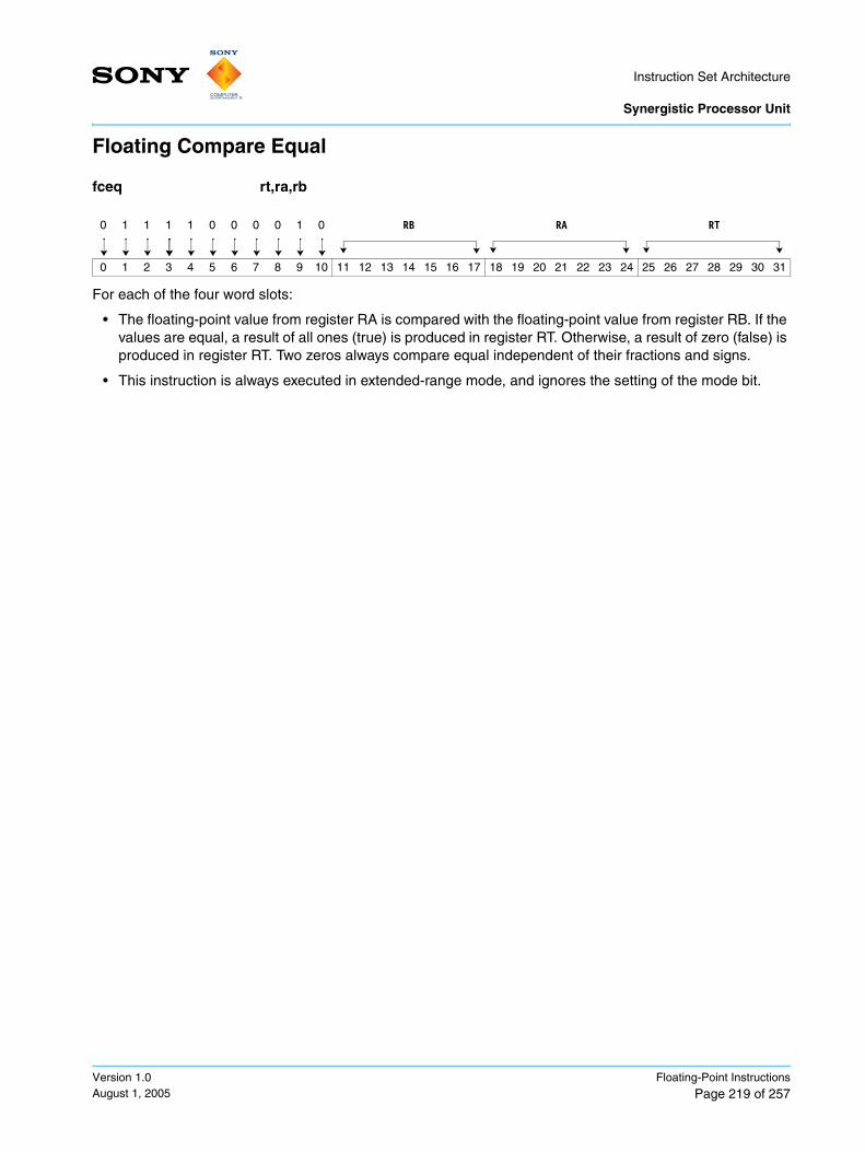
Instruction Set Architecture
Synergistic Processor Unit
Version 1.0August 1, 2005
Floating-Point Instructions
Page 219 of 257
Floating Compare Equal
For each of the four word slots:
• The floating-point value from register RA is compared with the floating-point value from register RB. If the values are equal, a result of all ones (true) is produced in register RT. Otherwise, a result of zero (false) is produced in register RT. Two zeros always compare equal independent of their fractions and signs.
• This instruction is always executed in extended-range mode, and ignores the setting of the mode bit.
fceq rt,ra,rb
0 1 1 1 1 0 0 0 0 1 0 RB RA RT
0 1 2 3 4 5 6 7 8 9 10 11 12 13 14 15 16 17 18 19 20 21 22 23 24 25 26 27 28 29 30 31

Instruction Set Architecture Synergistic Processor Unit
Floating-Point Instructions
Page 220 of 257Version 1.0
August 1, 2005
Floating Compare Magnitude Equal
For each of the four word slots:
• The absolute value of the floating-point number in register RA is compared with the absolute value of the floating-point number in register RB. If the absolute values are equal, a result of all ones (true) is pro-duced in register RT. Otherwise, a result of zero (false) is produced in register RT. Two zeros always com-pare equal independent of their fractions and signs.
• This instruction is always executed in extended-range mode, and ignores the setting of the mode bit.
fcmeq rt,ra,rb
0 1 1 1 1 0 0 1 0 1 0 RB RA RT
0 1 2 3 4 5 6 7 8 9 10 11 12 13 14 15 16 17 18 19 20 21 22 23 24 25 26 27 28 29 30 31

Instruction Set Architecture
Synergistic Processor Unit
Version 1.0August 1, 2005
Floating-Point Instructions
Page 221 of 257
Floating Compare Greater Than
For each of the four word slots:
• The floating-point value in register RA is compared with the floating-point value in register RB. If the value in RA is greater than the value in RB, a result of all ones (true) is produced in register RT. Otherwise, a result of zero (false) is produced in register RT. Two zeros never compare greater than independent of their sign bits and fractions.
• This instruction is always executed in extended-range mode, and ignores the setting of the mode bit.
fcgt rt,ra,rb
0 1 0 1 1 0 0 0 0 1 0 RB RA RT
0 1 2 3 4 5 6 7 8 9 10 11 12 13 14 15 16 17 18 19 20 21 22 23 24 25 26 27 28 29 30 31

Instruction Set Architecture Synergistic Processor Unit
Floating-Point Instructions
Page 222 of 257Version 1.0
August 1, 2005
Floating Compare Magnitude Greater Than
For each of the four word slots:
• The absolute value of the floating-point number in register RA is compared with the absolute value of the floating-point number in register RB. If the absolute value of the value from register RA is greater than the absolute value of the value from register RB, a result of all ones (true) is produced in register RT. Other-wise, a result of zero (false) is produced in register RT. Two zeros never compare greater than, indepen-dent of their fractions and signs.
• This instruction is always executed in extended-range mode, and ignores the setting of the mode bit.
fcmgt rt,ra,rb
0 1 0 1 1 0 0 1 0 1 0 RB RA RT
0 1 2 3 4 5 6 7 8 9 10 11 12 13 14 15 16 17 18 19 20 21 22 23 24 25 26 27 28 29 30 31

Instruction Set Architecture
Synergistic Processor Unit
Version 1.0August 1, 2005
Floating-Point Instructions
Page 223 of 257
Floating-Point Status and Control Register Write
The 128-bit value of register RA is written into the Floating-Point Status and Control Register (FPSCR). The value of the unused bits in the FPSCR is undefined. RT is a false target. Implementations can schedule instructions as though this instruction produces a value into RT. Programs can avoid unnecessary delay by programming RT so as not to appear to source data for nearby subsequent instructions. False targets are not written.
fscrwr ra
0 1 1 1 0 1 1 1 0 1 0 /// RA RT
0 1 2 3 4 5 6 7 8 9 10 11 12 13 14 15 16 17 18 19 20 21 22 23 24 25 26 27 28 29 30 31
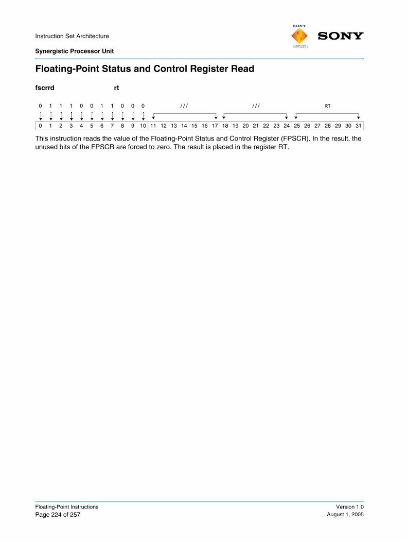
Instruction Set Architecture Synergistic Processor Unit
Floating-Point Instructions
Page 224 of 257Version 1.0
August 1, 2005
Floating-Point Status and Control Register Read
This instruction reads the value of the Floating-Point Status and Control Register (FPSCR). In the result, the unused bits of the FPSCR are forced to zero. The result is placed in the register RT.
fscrrd rt
0 1 1 1 0 0 1 1 0 0 0 /// /// RT
0 1 2 3 4 5 6 7 8 9 10 11 12 13 14 15 16 17 18 19 20 21 22 23 24 25 26 27 28 29 30 31

Instruction Set Architecture
Synergistic Processor Unit
Version 1.0August 1, 2005
Control Instructions
Page 225 of 257
10. Control Instructions
This section lists and describes the SPU control instructions.

Instruction Set Architecture Synergistic Processor Unit
Control Instructions
Page 226 of 257Version 1.0
August 1, 2005
Stop and Signal
Execution of the program in the SPU stops, and the external environment is signaled. No further instructions are executed.
stop
0 0 0 0 0 0 0 0 0 0 0 /// Stop and Signal Type
0 1 2 3 4 5 6 7 8 9 10 11 12 13 14 15 16 17 18 19 20 21 22 23 24 25 26 27 28 29 30 31
PC ← PC + 4 & LSLRprecise stop

Instruction Set Architecture
Synergistic Processor Unit
Version 1.0August 1, 2005
Control Instructions
Page 227 of 257
Stop and Signal with Dependencies
Execution of the program in the SPU stops.
Programming Note: This instruction differs from stop only in that, in typical implementations, instructions with dependencies can be replaced with stopd to create a breakpoint without affecting the instruction timings.
stopd
0 0 1 0 1 0 0 0 0 0 0 RB RA RC
0 1 2 3 4 5 6 7 8 9 10 11 12 13 14 15 16 17 18 19 20 21 22 23 24 25 26 27 28 29 30 31
PC ← PC + 4 & LSLRprecise stop

Instruction Set Architecture Synergistic Processor Unit
Control Instructions
Page 228 of 257Version 1.0
August 1, 2005
No Operation (Load)
This instruction has no effect on the execution of the program. It exists to provide implementation-defined control of instruction issuance. RT is a false target. Implementations can schedule instructions as though this instruction produces a value into RT. Programs can avoid unnecessary delay by programming RT so as not to appear to source data for nearby subsequent instructions. False targets are not written.
lnop
0 0 0 0 0 0 0 0 0 0 1 /// /// RT
0 1 2 3 4 5 6 7 8 9 10 11 12 13 14 15 16 17 18 19 20 21 22 23 24 25 26 27 28 29 30 31

Instruction Set Architecture
Synergistic Processor Unit
Version 1.0August 1, 2005
Control Instructions
Page 229 of 257
No Operation (Execute)
This instruction has no effect on the execution of the program. It exists to provide implementation-defined control of instruction issuance. RT is a false target. Implementations can schedule instructions as though this instruction produces a value into RT. Programs can avoid unnecessary delay by programming RT so as not to appear to source data for nearby subsequent instructions. False targets are not written.
nop
0 1 0 0 0 0 0 0 0 0 1 /// /// RT
0 1 2 3 4 5 6 7 8 9 10 11 12 13 14 15 16 17 18 19 20 21 22 23 24 25 26 27 28 29 30 31

Instruction Set Architecture Synergistic Processor Unit
Control Instructions
Page 230 of 257Version 1.0
August 1, 2005
Synchronize
This instruction has no effect on the execution of the program other than to cause the processor to wait until all pending store instructions have completed before fetching the next sequential instruction. This instruction must be used following a store instruction that modifies the instruction stream.
The C feature bit causes channel synchronization to occur before instruction synchronization occurs. Channel synchronization allows an SPU state modified through channel instructions to affect execution. Synchronization is discussed in more detail in Section 13 Synchronization and Ordering on page 240.
sync
0 0 0 0 0 0 0 0 0 1 0 C ///
0 1 2 3 4 5 6 7 8 9 10 11 12 13 14 15 16 17 18 19 20 21 22 23 24 25 26 27 28 29 30 31

Instruction Set Architecture
Synergistic Processor Unit
Version 1.0August 1, 2005
Control Instructions
Page 231 of 257
Synchronize Data
This instruction forces all earlier load, store, and channel instructions to complete before proceeding. No subsequent load, store, or channel instructions can start until the previous instructions complete. The dsync instruction allows SPU software to ensure that the local store data would be consistent if it were observed by another entity. This instruction does not affect any prefetching of instructions that the processor might have done. Synchronization is discussed in more detail in Section 13 Synchronization and Ordering on page 240.
dsync
0 0 0 0 0 0 0 0 0 1 1 /// /// ///
0 1 2 3 4 5 6 7 8 9 10 11 12 13 14 15 16 17 18 19 20 21 22 23 24 25 26 27 28 29 30 31

Instruction Set Architecture Synergistic Processor Unit
Control Instructions
Page 232 of 257Version 1.0
August 1, 2005
Move from Special-Purpose Register
Special-Purpose Register SA is copied into register RT. If SPR SA is not defined, zeros are supplied.
mfspr rt,sa
0 0 0 0 0 0 0 1 1 0 0 /// SA RT
0 1 2 3 4 5 6 7 8 9 10 11 12 13 14 15 16 17 18 19 20 21 22 23 24 25 26 27 28 29 30 31
if defined(SPR(SA)) thenRT ← SPR(SA)
elseRT ← 0

Instruction Set Architecture
Synergistic Processor Unit
Version 1.0August 1, 2005
Control Instructions
Page 233 of 257
Move to Special-Purpose Register
The contents of the preferred slot of register RT is written to Special-Purpose Register SA. If SPR SA is not defined, no operation is performed.
mtspr sa, rt
0 0 1 0 0 0 0 1 1 0 0 /// SA RT
0 1 2 3 4 5 6 7 8 9 10 11 12 13 14 15 16 17 18 19 20 21 22 23 24 25 26 27 28 29 30 31
if defined(SPR(SA)) thenSPR(SA) ← RT
elsedo nothing

Instruction Set Architecture Synergistic Processor Unit
Channel Instructions
Page 234 of 257Version 1.0
August 1, 2005
11. Channel Instructions
The SPU provides an input/output interface based on message passing called the “channel interface”. This section describes the instructions used to communicate between the SPU and external devices through the channel interface.
Channels are 128-bit wide communication paths between the SPU and external devices. Each channel oper-ates in one direction only, and is called either a read channel or a write channel, according to the operation that the SPU can perform on the channel. Instructions are provided that allow the SPU program to read from or write to a channel; the operations performed must match the type of channel addressed.
An implementation can implement any number of channels up to 128. Each channel has a channel number in the range 0-127. Channel numbers have no particular significance, and there is no relationship between the direction of a channel and its number.
The channels and the external devices have capacity. Channel capacity is the minimum number of reads or writes that can be performed without delay. Attempts to access a channel without capacity cause instruction processing to cease until capacity becomes available and the access can complete. The SPU maintains counters to measure channel capacity and provides an instruction to read channel capacity.
So long as capacity is available, the channels and external devices can service a burst of SPU accesses without requiring the SPU to delay execution. An attempt to write to a channel beyond its capacity causes the SPU to hang until the external device empties the channel. An attempt to read from a channel when it is empty also causes the SPU to hang until the device inserts data into the channel.

Instruction Set Architecture
Synergistic Processor Unit
Version 1.0August 1, 2005
Channel Instructions
Page 235 of 257
Read Channel
The SPU waits for data to become available in channel CA (capacity is available). When data is available to the channel, it is moved from the channel and placed into register RT.
If the channel designated by the CA field is not a valid, readable channel, the SPU will stop on or after the rdch instruction.
rdch rt,ca
0 0 0 0 0 0 0 1 1 0 1 /// CA RT
0 1 2 3 4 5 6 7 8 9 10 11 12 13 14 15 16 17 18 19 20 21 22 23 24 25 26 27 28 29 30 31
if readable(Channel(CA)) thenRT ← Channel(CA)
elseStop after executing zero or more instructions after the rdch.

Instruction Set Architecture Synergistic Processor Unit
Channel Instructions
Page 236 of 257Version 1.0
August 1, 2005
Read Channel Count
The channel capacity of channel CA is placed into the preferred slot of register RT. The channel capacity of unimplemented channels is zero.
rchcnt rt,ca
0 0 0 0 0 0 0 1 1 1 1 /// CA RT
0 1 2 3 4 5 6 7 8 9 10 11 12 13 14 15 16 17 18 19 20 21 22 23 24 25 26 27 28 29 30 31
RT0:3 ← Channel Capacity(CA)RT4:15 ← 0

Instruction Set Architecture
Synergistic Processor Unit
Version 1.0August 1, 2005
Channel Instructions
Page 237 of 257
Write Channel
The SPU waits for capacity to become available in channel CA before executing the wrch instruction. When capacity is available in the channel, the contents of register RT are placed into channel CA. Channel writes targeting channels that are not valid writable channels cause the SPU to stop on or after the wrch instruction.
wrch ca,rt
0 0 1 0 0 0 0 1 1 0 1 /// CA RT
0 1 2 3 4 5 6 7 8 9 10 11 12 13 14 15 16 17 18 19 20 21 22 23 24 25 26 27 28 29 30 31
if writeable(Channel(CA)) thenChannel(CA) ← RT
elseStop after executing zero or more instructions after the wrch.

Instruction Set Architecture Synergistic Processor Unit
SPU Interrupt Facility
Page 238 of 257Version 1.0
August 1, 2005
12. SPU Interrupt Facility
This section describes the SPU interrupt facility.
External conditions are monitored and managed through external facilities that are controlled through the channel interface. External conditions can affect SPU instruction sequencing through the following facilities:
• The bisled instruction
The bisled instruction tests for the existence of an external condition and branches to a target, if it is present. The bisled instruction allows the SPU software to poll for external conditions and to call a han-dler subroutine, if one is present. When polling is not required, the SPU can be enabled to interrupt nor-mal instruction processing and to vector to a handler subroutine when an external condition appears.
• The interrupt facility
The following indirect branch instructions allow software to enable and disable the interrupt facility during critical subroutines:
• bi• bisl• bisled• biz• binz• bihz• bihnz
All of these branch instructions provide the [D] and [E] feature bits. When one of these branches is taken, the interrupt-enable status changes before the target instruction is executed. Table 12-1 describes the feature bit settings and their results.
12.1 SPU Interrupt Handler
The SPU supports a single interrupt handler. The entry point for this handler is address 0 in local store. When a condition is present and interrupts are enabled, the SPU branches to address 0 and disables the interrupt facility. The address of the next instruction to be executed is saved in the SRR0 register. The iret instruction can be used to return from the handler. iret branches indirectly to the address held in the SRR0 register. iret, like the other indirect branches, has an [E] feature bit that can be used to re-enable interrupts.
Table 12-1. Feature Bits [D] and [E] Settings and Results
Feature Bit SettingResult
[D] [E]
0 0 Status does not change.
0 1 Interrupt processing is enabled.
1 0 Interrupt processing is disabled.
1 1 Causes undefined behavior.

Instruction Set Architecture
Synergistic Processor Unit
Version 1.0August 1, 2005
SPU Interrupt Facility
Page 239 of 257
12.2 SPU Interrupt Facility Channels
The interrupt facility uses several channels for configuration, state observation, and state restoration. The current value of SRR0 can be read from the SPU_RdSRR0 channel, and the SPU_WrSRR0 channel provides write access to SRR0. When SRR0 is written by wrch 14, synchronization is required to ensure that this new value is available to the iret instruction. This synchronization is provided by executing the sync instruction with the [C], or Channel Sync, feature bit set. Without this synchronization, iret instructions executed after wrch 14 instructions branch to unpredictable addresses. The SPU_RdSRR0 and SPU_WrSRR0 support nested interrupts by allowing software to save and restore SRR0 to a save area in local store.

Instruction Set Architecture Synergistic Processor Unit
Synchronization and Ordering
Page 240 of 257Version 1.0
August 1, 2005
13. Synchronization and Ordering
The SPU provides a sequentially ordered programming model so that, with a few exceptions, all previous instructions appear to be finished before the next instruction is started.
Systems including an SPU often feature external devices with direct local store access. Figure 13-1 shows a common organization in which the external devices also communicate with the SPU via the channel interface. These systems are shared memory multiprocessors with message passing.
Table 13-1 defines five transactions serviced by the local store. The SPU ISA does not define the behavior of the external device or how the external device accesses the local store. When this document refers to an external write of local store, it assumes the external device delivers data to the local store such that a subse-quent SPU load from local store can retrieve the data.
Interaction between the local store access of the external devices and those of the SPU can expose effects of SPU implementation-specific reordering, speculation, buffering, and caching. This section discusses how to order sequences of these transactions to obtain consistent results.
Figure 13-1. Systems with Multiple Accesses to Local Store
Table 13-1. Local Store Accesses
Name Description
Load SPU load instruction gets data from local store read.
Store SPU store instruction sends data to local store write.
Fetch SPU instruction fetch gets data from local store read.
ExtWrite External device sends data to local store write.
ExtRead External device gets data from local store read.
ExternalSPU
InstructionLoad Store ExtRead ExtWrite
Local Store
ChannelInterface
Fetch
Device

Instruction Set Architecture
Synergistic Processor Unit
Version 1.0August 1, 2005
Synchronization and Ordering
Page 241 of 257
13.1 Speculation, Reordering, and Caching SPU Local Store Access
SPU local store access is weakly consistent (see PowerPC Virtual Environment Architecture, Book II). There-fore, the sequential execution model, as applied to instructions that cause storage accesses, guarantees only that those accesses appear to be performed in program order with respect to the SPU executing the instruc-tions. These accesses might not appear to be performed in program order with respect to external local store accesses or with respect to the SPU instruction fetch. This means that, in the absence of external local store writes, an SPU load from any particular address returns the data written by the most recent SPU store to that address. However, an instruction fetch from that address does not necessarily return that data.
The SPU is allowed to cache, buffer, and otherwise reorder its local store accesses. SPU loads, stores, and instruction fetches might or might not access the local store. The SPU can speculatively read the local store. That is, the SPU can read the local store on behalf of instructions that are not required by the program. The SPU does not speculatively write the local store. If and when the SPU stores access the local store, the SPU only writes the local store on behalf of stores required by the program. Instruction fetches, loads, and stores can access the local store in any order.
13.2 Internal Execution State
The channel interface can be used to modify the SPU internal execution state. An internal execution state is any state within an SPU, but outside the local store, that is modified through the channel interface and that can affect the sequence or execution of instructions. For example, programs can change SRR0 by writing the SPU_WrSRR0 channel, and SRR0 is the internal execution state. State changes made through the channel interface might not be synchronized with SPU program execution.
13.3 Synchronization Primitives
The SPU provides three synchronization instructions: dsync, sync, and sync.c. These instructions have both coherency and instruction serializing effects, as shown in Table 13-2 Synchronization Instructions on page 242. Programs can use the coherency effects of these primitives to ensure that the local store state is consistent with SPU loads and stores. The instruction serializing effects allow the SPU program to order its local store access.
The dsync instruction orders loads, stores, and channel accesses but not instruction fetches. When a dsync completes, the SPU will have completed all prior loads, stores, and channel accesses and will not have begun execution of any subsequent loads, stores, or channel accesses. At this time, an external read from a local store address returns the data stored by the most recent SPU store to that address. SPU loads after the dsync return the data externally written prior to the moment when the dsync completes. The dsync instruc-tion affects only SPU instruction sequencing and the coherency of loads and stores with respect to actual local store state. The SPU does not broadcast dsync notification to external devices that access local store, and, therefore, does not affect the state of the external devices.
The sync instruction is much like dsync, but it also orders instruction fetches. Instruction fetches from a local store address after a sync instruction return data stored by the most recent store instruction or external write to that address. The sync.c instruction builds upon the sync instruction. It ensures that the effects upon the internal state caused by prior wrch instructions are propagated and influence the execution of the following instructions. SPU execution begins with a start event and ends with a stop event. Both start and stop perform sync.c.

Instruction Set Architecture Synergistic Processor Unit
Synchronization and Ordering
Page 242 of 257Version 1.0
August 1, 2005
Table 13-3 details which synchronization primitives are required between local store writes and local store reads to ensure that the reads access data written by the prior writes.
13.4 Caching SPU Local Store Access
Implementations of the SPU can feature caches of local store data for either instructions, data, or both. These caches must reflect data to and from the local store when synchronization requires the state of the local store to be consistent. The dsync instruction ensures that modified data is visible to external devices that access the local store, and that data modified by these external devices is visible to subsequent loads and stores. The sync instructions also ensure that data modified by either stores or external puts is visible to a subse-quent instruction fetch. For example, an instruction cache that does not snoop must be invalidated when sync is executed, and a copy-back data cache that does not snoop must be flushed and invalidated when either sync or dsync is executed.
Table 13-2. Synchronization Instructions
Instruction Coherency Effects Instruction Serialization Effects
dsync
Ensures that subsequent external reads access data written by prior stores.Ensures that subsequent loads access data written by external writes.
Forces load and store access of local store due to instruc-tions prior to the dsync to be completed prior to completion of dsync.Forces read channel operations due to instructions prior to the dsync to be completed prior to completion of the dsync.Forces load and store access of local store due to instruc-tions after the dsync to occur after completion of the dsync.Forces read and write channel operations due to instruc-tions after the dsync to occur after completion of the dsync.
sync
Ensures that subsequent external reads access data written by prior stores.Ensures that subsequent instruction fetches access data written by prior stores and external writes.Ensures that subsequent loads access data written by external writes.
Forces all access of local store and channels due to instruc-tions prior to the sync to be completed prior to completion of sync.Forces all access of local store and channels due to instruc-tions after the sync to occur after completion of the sync.
sync.c
Ensures that subsequent external reads access data written by prior stores.Ensures that subsequent instruction fetches access data written by prior stores and external writes.Ensures that subsequent loads access data written by external writes.Ensures that subsequent instruction processing is influ-enced by all internal execution states modified by previous wrch instructions.
Forces all access of local store and channels due to instruc-tions prior to the sync.c to be completed prior to completion of sync.c.Forces all access of local store and channels due to instruc-tions after the sync.c to occur after completion of the sync.c.
Table 13-3. Synchronizing Multiple Accesses to Local Store
Writer Store Fetch Load ExtRead
Store nothing sync nothing dsync
ExtWrite dsync sync dsync N/A

Instruction Set Architecture
Synergistic Processor Unit
Version 1.0August 1, 2005
Synchronization and Ordering
Page 243 of 257
13.5 Self-Modifying Code
SPU programs can store instructions in local store and execute them. If the SPU has already read the instruc-tions from local store, prior to the store, the new instructions are not seen by SPU execution. Self-modifying code should always execute a sync instruction before executing the stored code. The sync instruction ensures that all stores complete before the next instruction is fetched from local store.
13.6 External Local Store Access
Loads and stores do not necessarily access the local store in program order. Accesses from external devices can be interleaved in ways that are inconsistent with program order. The dsync instruction forces all preceding loads and stores to complete their local store access before allowing any further loads or stores to be initiated, while sync ensures that the next instruction is fetched after the sync instruction is executed. An external device can synchronize with an SPU program through local store access. Table 13-4 shows how an SPU program can reliably send and receive data from an external device, synchronizing only through the local store.
Table 13-4. Synchronizing through Local Store
ExternalDevice SPU Comment
SPU sends data through local store address C
Store data to C
dsync Force subsequent store to follow the store to C
Store marker to D
dsync Force the store to D to access the local store
eloop: Read D
If not marker goto eloop
Read C
SPU receives data through local store address A
Write data to AThis is the order in which the external device modifies local store. The ordering is not controlled by the SPU ISA.
Write marker to B
loop: dsync Force subsequent load to access local store
Load from B
If not marker goto loop Ensure A and B are both written to local store
dsync Force subsequent load to execute after load from B
Load from A Must get data

Instruction Set Architecture Synergistic Processor Unit
Synchronization and Ordering
Page 244 of 257Version 1.0
August 1, 2005
13.7 Speculation and Reordering of Channel Reads and Channel Writes
The SPU does not reorder or speculatively execute channel reads or channel writes. All operations at the channel interface represent instructions in the order they occur in the program.
13.8 Channel Interface with External Device
The channel interface delivers channel reads and writes to the SPU interface in program order, but there are no ordering guarantees with respect to load and stores. It is possible that a message sent to an external device may trigger the external device to directly access the local store. SPU programs might want to use either sync or dsync instructions, or both, to order SPU loads and stores relative to the external accesses. Table 13-5 shows how an SPU program might reliably send and receive data from an external device synchronizing through the channel interface.
Note: The SPU architecture does not specify what actions an external device can perform in response to a channel read or write. The SPU does not wait for those actions to complete, and it does not synchronize the local store state prior to or after the channel operation.
13.9 Execution State Set by an SPU Program through the Channel Interface
Some SPU channels can control aspects of SPU execution state; for example, SRR0. State changes made through channel writes might not affect subsequent instructions. Execution of the sync.c instruction ensures that the new state does affect the next instruction.
Table 13-5. Synchronizing through Channel Interface
ExternalDevice SPU Comment
SPU receives data through local store address A
Write data to A
Send message to channel B The ordering is not controlled by the SPU ISA.
rdch B Wait for message
dsync Ensure load from A is executed after rdch, and access the data in local store
load from A Must get data
SPU sends data through local store address C
Store data to C
dsync Ensure data is in local store
wrch D Send message
Receive message from channel D
Read data from C The ordering is not controlled by the SPU ISA.

Instruction Set Architecture
Synergistic Processor Unit
Version 1.0August 1, 2005
Synchronization and Ordering
Page 245 of 257
13.10 Execution State Set by an External Device
Execution state changes made by an external device are ordered with respect to other externally requested state changes but not with respect to SPU instruction execution. The external device can stop the SPU, make execution state changes, start the SPU, and be certain the new state is visible to program execution.

Instruction Set Architecture Synergistic Processor Unit
Synchronization and Ordering
Page 246 of 257Version 1.0
August 1, 2005

Instruction Set Architecture
Synergistic Processor Unit
Version 1.0August 1, 2005
Programming Examples
Page 247 of 257
Appendix A. Programming Examples
A.1 Conversion from Single Precision to Double Precision
This example converts four single-precision numbers in register rin to two double-precision numbers in each of rout and rout1.
shri.q rexph=rin,27 high order part of exponent as an integer
fceq.q rzero=rin,R0 Assumes r0=0; check for zero or denorm input
rotm.q rsign=rin,-31 Copy sign bit to bit 31
andi.q rexph=rexph,0b01111 Extract exponent bits 7 to 4
shli.q rsign=rsign,7 Rsign = 0…0 s 0^7
ai.q rexph= rexph,111000 Convert exponent to DP bias
shli.q rout=rin,5 Preshift of mantissa: e[3:0], f[1:23]^5
andc.q rexph=rexp,rzero Exponent cleared in case of zero/dernomal input
andc.q rout =rout,rzero Mantissa cleared in case of zero/dernomal input
or.q rexph=rexph,rsign Sign is ORed in, Rexp = (0…0, s g[10:4])
Nop Delay slot
shufb.q rout=rout,rexph,rindex First pair of DP results
shufb.q rout1=rout,rexph,rindex1 Second pair of DP results

Instruction Set Architecture Synergistic Processor Unit
Programming Examples
Page 248 of 257Version 1.0
August 1, 2005
A.2 Conversion from Double Precision to Single Precision
This example converts a double-precision number in the slot 0 of register rin to a single-precision value in the preferred slot of register rf.
or rhigh=rin,rin High order part copied
rotqbi rf=rin,3 Collect relevant mantissa bits (g[3:0], f[1:28])
rotm rhabs,rhigh,-1 Dropping the sign bit, shifted off the right end
rotm rsign,rhigh,-31 rsign = 0 … 0 s
rotm rexd, rhabs,-25 Extract exponent, rexp = 0…0 g[10:14]
rotm rf=rf,-5 Rf = 0^5, g[3:0], f[1:23]
ai rexs,rexd,8 rexp = rexp + 128/16
cgti Rmax, Rexd,71 rmax = -1 iff overflow; exponent > 128
andi rexs=rexs,’0 1^4’ Extract exponent bits, e[7:4]
cgt rmin,XMIN,rhabs rmin = 0 iff number to be truncated to 0
rotm rexs,rexs,-27 Align exponent for single-precision for-mat
rotm rsign=rsign,-31 rsign = s 0…0
A rf=rf,rexs Combine exponent and mantissa: 0, e[7:0], f[1:23]
cgt rmin=XMIN,rhabs rmin = 0 iff number to be truncated to 0
Nop
or Rf=Rf,rmax Set to 1…1 if rounded to Xmax
Nop Empty slot
And rf=rf,rmin Set to 0…0 if truncated to 0
Nop
or rf=rf,rsign OR in the sign bit

Instruction Set Architecture
Synergistic Processor Unit
Version 1.0August 1, 2005
Instruction Table Sorted by Instruction Mnemonic
Page 249 of 257
Appendix B. Instruction Table Sorted by Instruction Mnemonic
Table B-1. Instructions Sorted by Mnemonic (Page 1 of 6)
Mnemonic Instruction Page
a Add Word 55
absdb Absolute Differences of Bytes 87
addx Add Extended 61
ah Add Halfword 53
ahi Add Halfword Immediate 54
ai Add Word Immediate 56
and And 92
andbi And Byte Immediate 94
andc And with Complement 93
andhi And Halfword Immediate 95
andi And Word Immediate 96
avgb Average Bytes 86
bg Borrow Generate 65
bgx Borrow Generate Extended 66
bi Branch Indirect 173
bihnz Branch Indirect If Not Zero Halfword 184
bihz Branch Indirect If Zero Halfword 183
binz Branch Indirect If Not Zero 182
bisl Branch Indirect and Set Link 176
bisled Branch Indirect and Set Link if External Data 175
biz Branch Indirect If Zero 181
br Branch Relative 169
bra Branch Absolute 170
brasl Branch Absolute and Set Link 172
brhnz Branch If Not Zero Halfword 179
brhz Branch If Zero Halfword 180
brnz Branch If Not Zero Word 177
brsl Branch Relative and Set Link 171
brz Branch If Zero Word 178
cbd Generate Controls for Byte Insertion (d-form) 37
cbx Generate Controls for Byte Insertion (x-form) 38
cdd Generate Controls for Doubleword Insertion (d-form) 43
cdx Generate Controls for Doubleword Insertion (x-form) 44
ceq Compare Equal Word 155
ceqb Compare Equal Byte 151

Instruction Set Architecture Synergistic Processor Unit
Instruction Table Sorted by Instruction Mnemonic
Page 250 of 257Version 1.0
August 1, 2005
ceqbi Compare Equal Byte Immediate 152
ceqh Compare Equal Halfword 153
ceqhi Compare Equal Halfword Immediate 154
ceqi Compare Equal Word Immediate 156
cflts Convert Floating to Signed Integer 214
cfltu Convert Floating to Unsigned Integer 216
cg Carry Generate 62
cgt Compare Greater Than Word 161
cgtb Compare Greater Than Byte 157
cgtbi Compare Greater Than Byte Immediate 158
cgth Compare Greater Than Halfword 159
cgthi Compare Greater Than Halfword Immediate 160
cgti Compare Greater Than Word Immediate 162
cgx Carry Generate Extended 63
chd Generate Controls for Halfword Insertion (d-form) 39
chx Generate Controls for Halfword Insertion (x-form) 40
clgt Compare Logical Greater Than Word 167
clgtb Compare Logical Greater Than Byte 163
clgtbi Compare Logical Greater Than Byte Immediate 164
clgth Compare Logical Greater Than Halfword 165
clgthi Compare Logical Greater Than Halfword Immediate 166
clgti Compare Logical Greater Than Word Immediate 168
clz Count Leading Zeros 78
cntb Count Ones in Bytes 79
csflt Convert Signed Integer to Floating 213
cuflt Convert Unsigned Integer to Floating 215
cwd Generate Controls for Word Insertion (d-form) 41
cwx Generate Controls for Word Insertion (x-form) 42
dfa Double Floating Add 196
dfm Double Floating Multiply 200
dfma Double Floating Multiply and Add 202
dfms Double Floating Multiply and Subtract 206
dfnma Double Floating Negative Multiply and Add 207
dfnms Double Floating Multiply and Subtract 206
dfs Double Floating Subtract 198
dsync Synchronize Data 231
eqv Equivalent 109
Table B-1. Instructions Sorted by Mnemonic (Page 2 of 6)
Mnemonic Instruction Page

Instruction Set Architecture
Synergistic Processor Unit
Version 1.0August 1, 2005
Instruction Table Sorted by Instruction Mnemonic
Page 251 of 257
fa Floating Add 195
fceq Floating Compare Equal 219
fcgt Floating Compare Greater Than 221
fcmeq Floating Compare Magnitude Equal 220
fcmgt Floating Compare Magnitude Greater Than 222
fesd Floating Extend Single to Double 218
fi Floating Interpolate 212
fm Floating Multiply 199
fma Floating Multiply and Add 201
fms Floating Multiply and Subtract 205
fnms Floating Negative Multiply and Subtract 203
frds Floating Round Double to Single 217
frest Floating Reciprocal Estimate 208
frsqest Floating Reciprocal Absolute Square Root Estimate 210
fs Floating Subtract 197
fscrrd Floating-Point Status and Control Register Write 223
fscrwr Floating-Point Status and Control Register Read 224
fsm Form Select Mask for Words 82
fsmb Form Select Mask for Bytes 80
fsmbi Form Select Mask for Bytes Immediate 51
fsmh Form Select Mask for Halfwords 81
gb Gather Bits from Words 85
gbb Gather Bits from Bytes 83
gbh Gather Bits from Halfwords 84
hbr Hint for Branch (r-form) 186
hbra Hint for Branch (a-form) 187
hbrr Hint for Branch Relative 188
heq Halt If Equal 145
heqi Halt If Equal Immediate 146
hgt Halt If Greater Than 147
hgti Halt If Greater Than Immediate 148
hlgt Halt If Logically Greater Than 149
hlgti Halt If Logically Greater Than Immediate 150
il Immediate Load Word 48
ila Immediate Load Address 49
ilh Immediate Load Halfword 46
ilhu Immediate Load Halfword Upper 47
Table B-1. Instructions Sorted by Mnemonic (Page 3 of 6)
Mnemonic Instruction Page

Instruction Set Architecture Synergistic Processor Unit
Instruction Table Sorted by Instruction Mnemonic
Page 252 of 257Version 1.0
August 1, 2005
iohl Immediate Or Halfword Lower 50
iret Interrupt Return 174
lnop No Operation (Load) 228
lqa Load Quadword (a-form) 31
lqd Load Quadword (d-form) 29
lqr Load Quadword Instruction Relative (a-form) 32
lqx Load Quadword (x-form) 30
mfspr Move from Special-Purpose Register 232
mpy Multiply 67
mpya Multiply and Add 71
mpyh Multiply High 72
mpyhh Multiply High High 74
mpyhha Multiply High High and Add 75
mpyhhau Multiply High High Unsigned and Add 77
mpyhhu Multiply High High Unsigned 76
mpyi Multiply Immediate 69
mpys Multiply and Shift Right 73
mpyu Multiply Unsigned 68
mpyui Multiply Unsigned Immediate 70
mtspr Move to Special-Purpose Register 233
nand Nand 107
nop No Operation (Execute) 229
nor Nor 108
or Or 97
orbi Or Byte Immediate 99
orc Or with Complement 98
orhi Or Halfword Immediate 100
ori Or Word Immediate 101
orx Or Across 102
rchcnt Read Channel Count 236
rdch Read Channel 235
rot Rotate Word 124
roth Rotate Halfword 122
rothi Rotate Halfword Immediate 123
rothm Rotate and Mask Halfword 131
rothmi Rotate and Mask Halfword Immediate 132
roti Rotate Word Immediate 125
Table B-1. Instructions Sorted by Mnemonic (Page 4 of 6)
Mnemonic Instruction Page

Instruction Set Architecture
Synergistic Processor Unit
Version 1.0August 1, 2005
Instruction Table Sorted by Instruction Mnemonic
Page 253 of 257
rotm Rotate and Mask Word 133
rotma Rotate and Mask Algebraic Word 142
rotmah Rotate and Mask Algebraic Halfword 140
rotmahi Rotate and Mask Algebraic Halfword Immediate 141
rotmai Rotate and Mask Algebraic Word Immediate 143
rotmi Rotate and Mask Word Immediate 134
rotqbi Rotate Quadword by Bits 129
rotqbii Rotate Quadword by Bits Immediate 130
rotqby Rotate Quadword by Bytes 126
rotqbybi Rotate Quadword by Bytes from Bit Shift Count 128
rotqbyi Rotate Quadword by Bytes Immediate 127
rotqmbi Rotate and Mask Quadword by Bits 138
rotqmbii Rotate and Mask Quadword by Bits Immediate 139
rotqmby Rotate and Mask Quadword by Bytes 135
rotqmbybi Rotate and Mask Quadword Bytes from Bit Shift Count 137
rotqmbyi Rotate and Mask Quadword by Bytes Immediate 136
selb Select Bits 110
sf Subtract From Word 59
sfh Subtract From Halfword 57
sfhi Subtract From Halfword Immediate 58
sfi Subtract From Word Immediate 60
sfx Subtract From Extended 64
shl Shift Left Word 115
shlh Shift Left Halfword 113
shlhi Shift Left Halfword Immediate 114
shli Shift Left Word Immediate 116
shlqbi Shift Left Quadword by Bits 117
shlqbii Shift Left Quadword by Bits Immediate 118
shlqby Shift Left Quadword by Bytes 119
shlqbybi Shift Left Quadword by Bytes from Bit Shift Count 121
shlqbyi Shift Left Quadword by Bytes Immediate 120
shufb Shuffle Bytes 111
stop Stop and Signal 226
stopd Stop and Signal with Dependencies 227
stqa Store Quadword (a-form) 35
stqd Store Quadword (d-form) 33
stqr Store Quadword Instruction Relative (a-form) 36
Table B-1. Instructions Sorted by Mnemonic (Page 5 of 6)
Mnemonic Instruction Page

Instruction Set Architecture Synergistic Processor Unit
Instruction Table Sorted by Instruction Mnemonic
Page 254 of 257Version 1.0
August 1, 2005
stqx Store Quadword (x-form) 34
sumb Sum Bytes into Halfwords 88
sync Synchronize 230
wrch Write Channel 237
xor Exclusive Or 103
xorbi Exclusive Or Byte Immediate 104
xorhi Exclusive Or Halfword Immediate 105
xori Exclusive Or Word Immediate 106
xsbh Extend Sign Byte to Halfword 89
xshw Extend Sign Halfword to Word 90
xswd Extend Sign Word to Doubleword 91
Table B-1. Instructions Sorted by Mnemonic (Page 6 of 6)
Mnemonic Instruction Page

Instruction Set Architecture
Synergistic Processor Unit
Version 1.0August 1, 2005
Details of the Compute-Mask Instructions
Page 255 of 257
Appendix C. Details of the Compute-Mask Instructions
The tables in this section show the details of the masks that are generated by the eight Compute Mask instructions. The masks that are shown are intended for use as the RC operand of the Shuffle Bytes, shufb, instruction. Each row in a table shows the rightmost 4 bits of the effective address. An x in the first column indicates an ignored bit. Blanks within the “created mask” are shown only to improve clarity.
For byte insertion:
For halfword insertion:
Table C-1. Byte Insertion: Rightmost 4 Bits of the Effective Address and Created Mask
Rightmost 4 Bits of the Effective Address Created Mask
0000 03 11 12 13 14 15 16 17 18 19 1a 1b 1c 1d 1e 1f
0001 10 03 12 13 14 15 16 17 18 19 1a 1b 1c 1d 1e 1f
0010 10 11 03 13 14 15 16 17 18 19 1a 1b 1c 1d 1e 1f
0011 10 11 12 03 14 15 16 17 18 19 1a 1b 1c 1d 1e 1f
0100 10 11 12 13 03 15 16 17 18 19 1a 1b 1c 1d 1e 1f
0101 10 11 12 13 14 03 16 17 18 19 1a 1b 1c 1d 1e 1f
0110 10 11 12 13 14 15 03 17 18 19 1a 1b 1c 1d 1e 1f
0111 10 11 12 13 14 15 16 03 18 19 1a 1b 1c 1d 1e 1f
1000 10 11 12 13 14 15 16 17 03 19 1a 1b 1c 1d 1e 1f
1001 10 11 12 13 14 15 16 17 18 03 1a 1b 1c 1d 1e 1f
1010 10 11 12 13 14 15 16 17 18 19 03 1b 1c 1d 1e 1f
1011 10 11 12 13 14 15 16 17 18 19 1a 03 1c 1d 1e 1f
1100 10 11 12 13 14 15 16 17 18 19 1a 1b 03 1d 1e 1f
1101 10 11 12 13 14 15 16 17 18 19 1a 1b 1c 03 1e 1f
1110 10 11 12 13 14 15 16 17 18 19 1a 1b 1c 1d 03 1f
1111 10 11 12 13 14 15 16 17 18 19 1a 1b 1c 1d 1e 03
Table C-2. Halfword Insertion: Rightmost 4 Bits of the Effective Address and Created Mask
Rightmost 4 Bits of the Effective Address Created Mask
000x 0203 1213 1415 1617 1819 1a1b 1c1d 1e1f
001x 1011 0203 1415 1617 1819 1a1b 1c1d 1e1f
010x 1011 1213 0203 1617 1819 1a1b 1c1d 1e1f
011x 1011 1213 1415 0203 1819 1a1b 1c1d 1e1f
100x 1011 1213 1415 1617 0203 1a1b 1c1d 1e1f
101x 1011 1213 1415 1617 1819 0203 1c1d 1e1f
110x 1011 1213 1415 1617 1819 1a1b 0203 1e1f
111x 1011 1213 1415 1617 1819 1a1b 1c1d 0203

Instruction Set Architecture Synergistic Processor Unit
Details of the Compute-Mask Instructions
Page 256 of 257Version 1.0
August 1, 2005
For word insertion:
For doubleword insertion:
Table C-3. Word Insertion: Rightmost 4 Bits of the Effective Address and Created Mask
Rightmost 4 Bits of the Effective Address Created Mask
00xx 00010203 14151617 18191a1b 1c1d1e1f
01xx 10111213 00010203 18191a1b 1c1d1e1f
10xx 10111213 14151617 00010203 1c1d1e1f
11xx 10111213 14151617 18191a1b 00010203
Table C-4. Doubleword Insertion: Rightmost 4 Bits of Effective Address and Created Mask
Rightmost 4 Bits of the Effective Address Created Mask
0xxx 0001020304050607 18191a1b1c1d1e1f
1xxx 1011121303151617 0001020304050607

Instruction Set Architecture
Synergistic Processor Unit
Version 1.0August 1, 2005
Revision Log
Page 257 of 257
Revision Log
Revision Date Contents of Modification
August 1, 2005 Initial public release.