surface passivation and interface properties of bulk gaas and epitaxial-gaas/ge using atomic layer...
TRANSCRIPT

Surface Passivation and Interface Properties of Bulk GaAs andEpitaxial-GaAs/Ge Using Atomic Layer Deposited TiAlO AlloyDielectricG. K. Dalapati,*,† C. K. Chia,† C. C. Tan,† H. R. Tan,† S. Y. Chiam,† J. R. Dong,‡ A. Das,§,∥
S. Chattopadhyay,§,∥ C. Mahata,⊥ C. K. Maiti,⊥ and D. Z. Chi*,†
†Institute of Materials Research and Engineering, A*STAR (Agency for Science, Technology and Research), 3 Research Link,Singapore 117602‡Suzhou Institute of Nano-Tech and Nano-Bionics, Chinese Academy of Sciences, 398 Ruoshui Road, Suzhou Industrial Park, Jiangsu215125, China§Department of Electronic Science, University of Calcutta, 92-A. P. C. Road, Kolkata, India 700 009∥Centre for Research in Nanoscience and Nanotechnology (CRNN), University of Calcutta, JD-2 Sector III, Kolkata, India 700 098⊥Department of Electronics and ECE, Indian Institute of Technology-Kharagpur, India 721302
ABSTRACT: High quality surface passivation on bulk-GaAssubstrates and epitaxial-GaAs/Ge (epi-GaAs) layers wereachieved by using atomic layer deposited (ALD) titaniumaluminum oxide (TiAlO) alloy dielectric. The TiAlO alloydielectric suppresses the formation of defective native oxide onGaAs layers. X-ray photoelectron spectroscopy (XPS) analysisshows interfacial arsenic oxide (AsxOy) and elemental arsenic(As) were completely removed from the GaAs surface. Energydispersive X-ray diffraction (EDX) analysis and secondary ionmass spectroscopy (SIMS) analysis showed that TiAlOdielectric is an effective barrier layer for reducing the out-diffusion of elemental atoms, enhancing the electrical properties ofbulk-GaAs based metal-oxide-semiconductor (MOS) devices. Moreover, ALD TiAlO alloy dielectric on epi-GaAs with AlGaAsbuffer layer realized smooth interface between epi-GaAs layers and TiAlO dielectric, yielding a high quality surface passivation onepi-GaAs layers, much sought-after for high-speed transistor applications on a silicon platform. Presence of a thin AlGaAs bufferlayer between epi-GaAs and Ge substrates improved interface quality and gate dielectric quality through the reduction ofinterfacial layer formation (GaxOy) and suppression of elemental out-diffusion (Ga and As). The AlGaAs buffer layer and TiAlOdielectric play a key role to suppress the roughening, interfacial layer formation, and impurity diffusion into the dielectric, whichin turn largely enhances the electrical property of the epi-GaAs MOS devices.
KEYWORDS: III−V surface passivation, atomic layer deposition, TiAlO alloy dielectric, epi-GaAs/Ge, effective dielectric constant,hysteresis voltage, elemental out-diffusion, GaAs MOS
■ INTRODUCTION
Development of epitaxial III−V high mobility channel materialson a silicon (Si) platform is much sought-after to realizecomplementary metal oxide semiconductor (CMOS) deviceswith increased carrier mobility and device flexibility.1−4
Gallium-arsenide (GaAs) and germanium (Ge) have receivedmuch attention in this respect due to their lower effective massand hence intrinsic superior transport property than Si.4 It isalso possible to grow epitaxial GaAs (epi-GaAs) on Gesubstrate to realize high performance, flexibility, and enhancedfunctionality of III−V compounds coupled with the lowmanufacturing cost and sheer scale of the silicon process.1−5
For an example, Liu et al. demonstrated long-wavelength InAs/GaAs quantum-dot laser diode monolithically grown on Gesubstrate.5 Performance gains using an epitaxial layer as achannel material are still challenging due to the deleterious
effects from the surface roughness and poor interface qualitybetween the epitaxial layer and gate dielectric. The loss ofcarrier recombination at the surface and interface of GaAs/gatedielectric not only degrades the characteristics of minority-carrier injection devices but also reduces the device lifetime,due to the presence of poor quality native oxide. Therefore,development of high-quality interface with an epi-GaAs channelmaterial is among the most challenging problems in modernsemiconductor technology.1−4
Even though several approaches had been made to realizehigh quality interface on bulk-GaAs substrates using highpermittivity (high-k) dielectrics and interfacial passivation
Received: November 7, 2012Accepted: January 18, 2013Published: January 18, 2013
Research Article
www.acsami.org
© 2013 American Chemical Society 949 dx.doi.org/10.1021/am302537b | ACS Appl. Mater. Interfaces 2013, 5, 949−957
layers (IPL),6−16 there have been continuous efforts to improvethe interface quality further. In addition, it is necessary to findthe suitable dielectric which is also compatible with germaniumsubstrates. For directly deposited high-k dielectric on GaAssubstrates, large interface defects and high hysteresis voltage incapacitance−voltage characteristics were observed. Much effortwill be needed to improve the interface quality between epi-GaAs and high-k dielectrics. The epi-GaAs has unusually highsurface roughness (∼5 nm) compared with bulk-GaAssubstrates and conventional Si substrates (∼0.3 nm).17 Thisleads to the formation of thick defective native oxides; as aresult, the electrical properties of MOS devices degraded.6,17,18
It is well-known that the atomic layer deposited (ALD)dielectrics offer a unique opportunity to passivate bulk-GaAsand epi-GaAs layers using high-k dielectrics.6,11−16,19 Inparticular, ALD is very crucial for epi-GaAs systems comparedto the other deposition technique, since it provides betterinterface between epi-GaAs and dielectric through conformalcoating of the epi-GaAs layers.14 Even though the ALD HfO2and Al2O3/TiO2 dielectrics on epi-GaAs show promisingresults, the frequency dispersion and hysteresis voltage in C−V characteristics are high.14,15 The alloy dielectric of Al2O3 andTiO2 (TiAlO) is a very promising dielectric due to its highdielectric constant and high thermal stability.20 It has beenmainly studied for Si- and Ge-based devices for high-k gatestacks,20−22 while there is considerably less work related to thesurface passivation of GaAs using TiAlO dielectric.23,24 In thepresent work, we have investigated the surface passivation ofbulk GaAs substrates and epi-GaAs layer using TiAlO gatedielectric. Gate dielectric quality and interfacial layer formationbetween TiAlO/GaAs have been discussed in detailed by usingX-ray photoelectron spectroscopy (XPS) and secondary ion
mass spectroscopy (SIMS). The elemental out-diffusion of Gaand As into TiAlO dielectric was studied using high-resolutiontransmission electron microscopy (HR-TEM) analysis andelectrical properties. In addition, we have also simulatedcapacitance−voltage (C−V) characteristic and compared themwith experimental results to determine the interfacial layerthickness and dielectric constant of the interfacial layer.
■ EXPERIMENTAL SECTIONA thin layer of TiAlO dielectric (∼14 nm) was deposited on the epi-GaAs layer and bulk-GaAs substrates. The epi-GaAs are grown at 675°C by using the metal−organic chemical-vapor-deposition (MOCVD)technique on Ge(100) substrates with 6° off-cut toward the (111)plane. The surface native oxide of Ge substrate was removed at 720 °Cin H2 ambient. After that, the temperature is ramped down to 675 °Cto grow a thin AlGaAs (10 nm) buffer layer on the Ge substrates.AsH3, TMGa, and TMAl are introduced into the reactor for thegrowth of the AlGaAs buffer layer and 500 nm thick epi-GaAs layer.The details of the epi-GaAs layer that was grown can be found in ref17. Prior to the deposition of ALD TiAlO dielectric, the as-grown epi-GaAs layers and bulk p-type GaAs substrates are degreased usingisopropanol, cleaned in HF solution (1%) for 3 min, and then dippedin NH4OH solution for 10 min. Thin TiAlO films are deposited usingalternative cycles of ALD of Al2O3 and TiO2 with a starting layer ofAl2O3. Al2O3 is deposited on epi-GaAs and bulk-GaAs usingtrimethylaluminium (TMA, SAFC Hitech, 99.9%) and H2O as theprecursors in viscous flow type (0.6 Torr working pressure) ALDequipment with a N2 flow rate of 50 sccm at 170 °C. Vapors of TiCl4(Merck, 99%) and H2O precursors are sequentially introduced into thechamber for the TiO2 deposition. For XPS analysis, a TiAlO thin filmof ∼5 nm thickness was deposited on bulk-GaAs and the epi-GaAslayer using the same process recipe. Postdeposition annealing (PDA)was carried out in a N2 ambient at 500 °C for 1 min by rapid thermalannealing (RTA) technique.
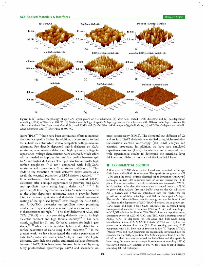
Figure 1. (a) Surface morphology of epi-GaAs layers grown on Ge substrates: (b) after ALD coated TiAlO dielectric and (c) postdepositionannealing (PDA) of TiAlO at 500 °C. (d) Surface morphology of epi-GaAs layers grown on Ge substrates with AlGaAs buffer layer between Gesubstrates and epi-GaAs layers: (e) after ALD coated TiAlO and (f) after PDA. AFM images of (g) bulk-GaAs, (h) ALD TiAlO deposition on bulk-GaAs substrates, and (i) after PDA at 500 °C.
ACS Applied Materials & Interfaces Research Article
dx.doi.org/10.1021/am302537b | ACS Appl. Mater. Interfaces 2013, 5, 949−957950
■ RESULTS AND DISCUSSION
The surface roughness of epi-GaAs and bulk p-GaAs wasmeasured using atomic force microscopy (AFM). The surfacetopography of epi-GaAs/Ge is nonuniform; it varies with thescan areas. Figure 1a shows the surface topography of epi-GaAsover the area of 10 × 10 μm2. The root-mean-square (rms)surface roughness is high, and the value is ∼6 nm with a distincttriangular feature. These triangular features are typical of epi-GaAs grown directly on Ge(100) substrates with 6° off-cuttoward the ⟨111⟩ direction. On a closer look with the scan areaof 1 × 1 μm2 (not shown), the surface roughness of epi-GaAshas a lower value compared with the large area (10 × 10 μm2).This suggests that the epi-GaAs has nonuniform surfacetopography, which also leads high surface roughness of ALDcoated TiAlO on the epi-GaAs layer. The surface roughness forALD coated TiAlO on the epi-GaAs layer was found to be inthe range of ∼6.6−7.2 nm over the scan area of 10 × 10 μm2
(Figure 1b,c). On the other hand, the epi-GaAs layers with
AlGaAs buffer layers reveals excellent surface morphology withlow rms roughness of ∼0.68 nm over the scan area of 1 × 1μm2, and the rms value remains same over the large area.Moreover, the surface roughness varies slightly between 0.65 to0.71 nm with ALD coated TiAlO dielectric (Figure 1d−f). It isworthwhile to note that the surface morphology for epi-GaAswith AlGaAs buffer layer is comparable with bulk-GaAssubstrates. The TiAlO dielectric on bulk p-GaAs substrateshows rms roughness of 0.23 −0.30 nm (Figure 1g−i). Thesurface roughness of bulk-GaAs with ALD coated TiAlO is verylow, and the value is typically observed for Si based MOSdevices. Furthermore, this rms value is lower compared withthe reported results on ALD Al2O3 deposited on similarchemically treated bulk-GaAs substrates.12 Low surface rough-ness of TiAlO on epi-GaAs with AlGaAs buffer layers revealsbetter surface morphology compared with epi-GaAs directlygrown on Ge substrates. This is due to the strain compensationat the GaAs/AlGaAs interface and AlGaAs/Ge interfaces.17 Thesmooth and uniform surface morphology of epi-GaAs layers
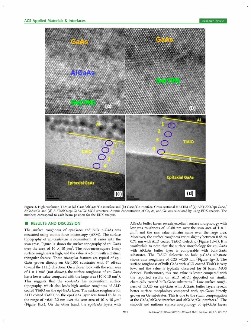
Figure 2. High resolution TEM at (a) GaAs/AlGaAs/Ge interface and (b) GaAs/Ge interface. Cross-sectional HRTEM of (c) Al/TiAlO/epi-GaAs/AlGaAs/Ge and (d) Al/TiAlO/epi-GaAs/Ge MOS structure. Atomic concentration of Ga, As, and Ge was calculated by using EDX analysis. Thenumbers correspond to each beam position for the EDX analysis.
ACS Applied Materials & Interfaces Research Article
dx.doi.org/10.1021/am302537b | ACS Appl. Mater. Interfaces 2013, 5, 949−957951
with AlGaAs buffer layer provides a platform to integrate high-kdielectrics for epi-GaAs/Ge based device application. The epi-GaAs/Ge based device requires high quality interface betweenhigh-k dielectric and epi-GaAs layers. Generally, the interfacequality depends on the surface morphology of the startinglayers. To the best of our knowledge, by using ALD TiAlOdielectric and epi-GaAs with AlGaAs buffer layer, we haveachieved uniform films with lowest surface roughness for epi-GaAs based gate stacks. Moreover, that the surface roughness ofTiAlO continues to remain the same even upon annealingreveals good thermal stability of the TiAlO/epi-GaAs/AlGaAs/Ge stacks.The high resolution transmission electron microscopy
(HRTEM) analysis is performed to investigate the interfaceproperties and TiAlO dielectric quality on epi-GaAs layers withand without AlGaAs buffer layers. The ALD TiAlO dielectricwas deposited on high quality epi-GaAs layer. The epi-GaAslayer was grown on Ge substrate with AlGaAs and withoutAlGaAs buffer layer, as shown in Figure 2a,b, respectively. Thecorresponding high-resolution TEM images at the interfacebetween TiAlO and the epi-GaAs layer are shown in Figure2c,d. For TiAlO/epi-GaAs/AlGaAs/Ge structure, the thicknessof TiAlO is ∼14 nm as shown in Figure 2c, which increased to15.5 nm for TiAlO/epi-GaAs/Ge due to higher surfaceroughness of the epi-GaAs layers grown directly on Gesubstrates without any buffer layer. According to Kim et al.25
the growth rate in ALD processes strongly depends on thedensity of functional groups on the reaction surface. It has beenconfirmed from the experiments that the saturated density offunctional groups on the semiconductor reaction surface ischanged during ALD growth. Thus, due to higher surfaceroughness, epi-GaAs exhibited a higher density of surfacehydroxyl groups which further enhance the film thickness ofTiAlO dielectric.12,25 Thus for the scale device, it is necessary toreduce the surface roughness of the epi-GaAs layer.A clear and sharp interface between TiAlO and epi-GaAs
layers was observed for the epi-GaAs with AlGaAs buffer layer,as shown in Figure 2c,d, respectively. According to theHRTEM images, the TiAlO film is amorphous in nature evenafter annealing at 500 °C. This is due to the presence of Al2O3in TiO2 films, which retains a high permittivity close to that ofTiO2 and also has excellent thermal stability like that ofAl2O3.
20 From the line energy dispersive X-ray analysis for thealloy gate stacks, the atomic concentration of Al and Ti is foundto be ∼28% and 21%, respectively. The incorporation ofelemental Ga and As into the dielectric is believed to beresponsible for the degradation of electrical properties of theMOS device.6,18 Therefore, the out-diffused elemental atomsare also a major concern for the reliability of the device. Theinterface quality as well as dielectric quality degrades due to thetraps created by the out-diffusion of the elemental Ga and Asatoms. The percentile amount of elemental Ga and As atdifferent positions of TiAlO dielectric is measured by EDXanalysis. The result shows that a very low amount of Ga diffusesinto the dielectric. There is almost no presence of elemental Asin the dielectric. Thus, TiAlO dielectric is able to reduce theout-diffusion of elemental Ga and As. This is due to the Tiincorporation into Al2O3, which acts as a barrier to elementaldiffusion of Ga and As into the dielectric.23The amount ofelemental Ga present in the TiAlO dielectric is also much lowercompared with the alloy dielectric of HfO2 and Al2O3 (HfAlO)deposited on the p-GaAs substrates.6 It is worth noting that thepercentile amount of Ga and As decreases further with the
presence of thin AlGaAs buffer layers for the epi-GaAs layer, asshown in Table 1. The ALD TiAlO dielectric not only improves
the interface quality by reducing the formation of defectivenative oxides (gallium-arsenide oxide) but also reduces the out-diffusion of elemental Ga and As, which are mainly responsiblefor increase oxide trap charges in the dielectric. Thin ILbetween TiAlO and the epi-GaAs layer (1.2 nm) was observedwhere epi-GaAs was grown directly on Ge substrates. On theother hand, there is no distinguishable IL between TiAlO andthe epi-GaAs interface, where epi-GaAs was grown on Gesubstrates with AlGaAs buffer layer. The combination of TiAlOdielectric and epi-GaAs with AlGaAs buffer layer plays a crucialrole to suppress the out-diffusion of elemental atoms into thedielectric, which mainly degrades electrical performance of thedevices.The interface chemical state of the ALD TiAlO alloy
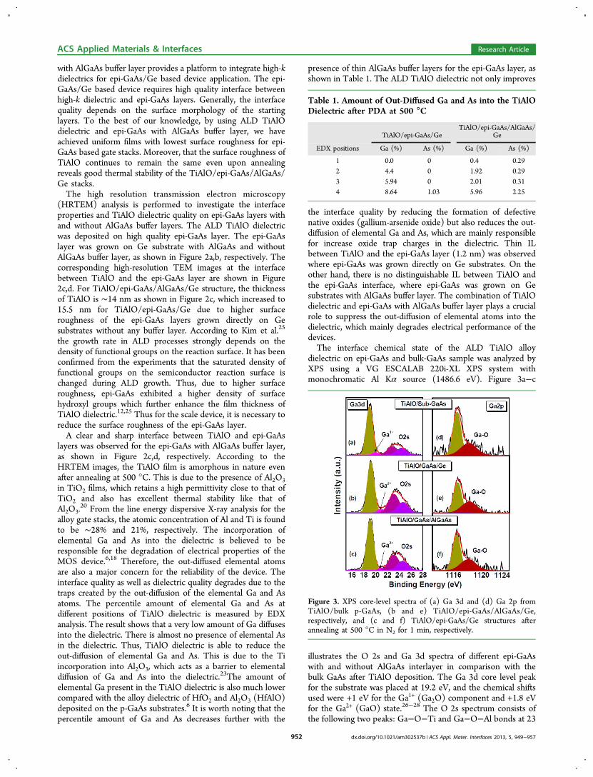
dielectric on epi-GaAs and bulk-GaAs sample was analyzed byXPS using a VG ESCALAB 220i-XL XPS system withmonochromatic Al Kα source (1486.6 eV). Figure 3a−c
illustrates the O 2s and Ga 3d spectra of different epi-GaAswith and without AlGaAs interlayer in comparison with thebulk GaAs after TiAlO deposition. The Ga 3d core level peakfor the substrate was placed at 19.2 eV, and the chemical shiftsused were +1 eV for the Ga1+ (Ga2O) component and +1.8 eVfor the Ga2+ (GaO) state.26−28 The O 2s spectrum consists ofthe following two peaks: Ga−O−Ti and Ga−O−Al bonds at 23
Table 1. Amount of Out-Diffused Ga and As into the TiAlODielectric after PDA at 500 °C
TiAlO/epi-GaAs/GeTiAlO/epi-GaAs/AlGaAs/
Ge
EDX positions Ga (%) As (%) Ga (%) As (%)
1 0.0 0 0.4 0.292 4.4 0 1.92 0.293 5.94 0 2.01 0.314 8.64 1.03 5.96 2.25
Figure 3. XPS core-level spectra of (a) Ga 3d and (d) Ga 2p fromTiAlO/bulk p-GaAs, (b and e) TiAlO/epi-GaAs/AlGaAs/Ge,respectively, and (c and f) TiAlO/epi-GaAs/Ge structures afterannealing at 500 °C in N2 for 1 min, respectively.
ACS Applied Materials & Interfaces Research Article
dx.doi.org/10.1021/am302537b | ACS Appl. Mater. Interfaces 2013, 5, 949−957952
eV and 24.5 eV attributed to formation of mix bonding in theinterface. As the electron affinity of Al is quit higher that of Ti,we have assumed that the higher O 2s peak is related with Al−O−Ga. The O 2s spectra of these samples are close to theprevious reported results.29 From the Ga 3d spectrum it isevident that the Ga−O feature has multiple oxidation states fordifferent samples including Ga1+ and Ga2+ probably due toGa2O and GaO formation. It is important to note that theTiAlO deposition has resulted in a Ga−O peak that is centeredat a lower binding energy for bulk GaAs samples. But for epi-GaAs/AlGaAs/Ge and epi-GaAs/Ge the resulting Ga−Ofeature with low intensity presents in the higher energyposition. According to Hinkle et al.30 binding energy may shiftdue to charge redistribution from second nearest neighborchanges in the Ga−O bonding environment. In our previousstudy, we have also found that there was a very thin interfaciallayer of Ga2O on the surface of bulk-GaAs for ALD HfO2;however, for epi-GaAs with high surface roughness (∼5 nm),the interface is distorted and shows a higher oxidation state ofGa, which is more closely related to the interface defectsformation.14,26 Suppressing the formation of Ga2Ox nativeoxide at the interface is important for epi-GaAs based devices toimprove the interface quality. The formation of Ga2Ox nativeoxide is also due to the intrinsic nature of n-type GaAssubstrate.6 Therefore, it is possible to suppress the formation ofGa2Ox native oxide at the interface by using p-type epi-GaAslayer with smooth surface morphology.Accurate identification of the 2p peak is more important,
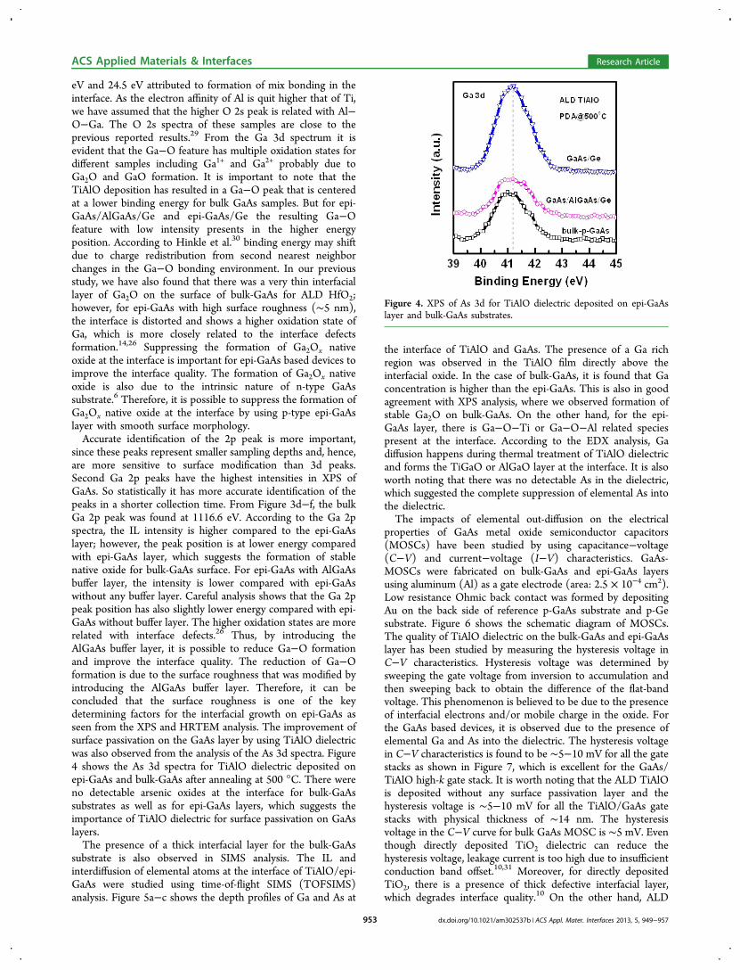
since these peaks represent smaller sampling depths and, hence,are more sensitive to surface modification than 3d peaks.Second Ga 2p peaks have the highest intensities in XPS ofGaAs. So statistically it has more accurate identification of thepeaks in a shorter collection time. From Figure 3d−f, the bulkGa 2p peak was found at 1116.6 eV. According to the Ga 2pspectra, the IL intensity is higher compared to the epi-GaAslayer; however, the peak position is at lower energy comparedwith epi-GaAs layer, which suggests the formation of stablenative oxide for bulk-GaAs surface. For epi-GaAs with AlGaAsbuffer layer, the intensity is lower compared with epi-GaAswithout any buffer layer. Careful analysis shows that the Ga 2ppeak position has also slightly lower energy compared with epi-GaAs without buffer layer. The higher oxidation states are morerelated with interface defects.26 Thus, by introducing theAlGaAs buffer layer, it is possible to reduce Ga−O formationand improve the interface quality. The reduction of Ga−Oformation is due to the surface roughness that was modified byintroducing the AlGaAs buffer layer. Therefore, it can beconcluded that the surface roughness is one of the keydetermining factors for the interfacial growth on epi-GaAs asseen from the XPS and HRTEM analysis. The improvement ofsurface passivation on the GaAs layer by using TiAlO dielectricwas also observed from the analysis of the As 3d spectra. Figure4 shows the As 3d spectra for TiAlO dielectric deposited onepi-GaAs and bulk-GaAs after annealing at 500 °C. There wereno detectable arsenic oxides at the interface for bulk-GaAssubstrates as well as for epi-GaAs layers, which suggests theimportance of TiAlO dielectric for surface passivation on GaAslayers.The presence of a thick interfacial layer for the bulk-GaAs
substrate is also observed in SIMS analysis. The IL andinterdiffusion of elemental atoms at the interface of TiAlO/epi-GaAs were studied using time-of-flight SIMS (TOFSIMS)analysis. Figure 5a−c shows the depth profiles of Ga and As at
the interface of TiAlO and GaAs. The presence of a Ga richregion was observed in the TiAlO film directly above theinterfacial oxide. In the case of bulk-GaAs, it is found that Gaconcentration is higher than the epi-GaAs. This is also in goodagreement with XPS analysis, where we observed formation ofstable Ga2O on bulk-GaAs. On the other hand, for the epi-GaAs layer, there is Ga−O−Ti or Ga−O−Al related speciespresent at the interface. According to the EDX analysis, Gadiffusion happens during thermal treatment of TiAlO dielectricand forms the TiGaO or AlGaO layer at the interface. It is alsoworth noting that there was no detectable As in the dielectric,which suggested the complete suppression of elemental As intothe dielectric.The impacts of elemental out-diffusion on the electrical
properties of GaAs metal oxide semiconductor capacitors(MOSCs) have been studied by using capacitance−voltage(C−V) and current−voltage (I−V) characteristics. GaAs-MOSCs were fabricated on bulk-GaAs and epi-GaAs layersusing aluminum (Al) as a gate electrode (area: 2.5 × 10⁻⁴ cm2).Low resistance Ohmic back contact was formed by depositingAu on the back side of reference p-GaAs substrate and p-Gesubstrate. Figure 6 shows the schematic diagram of MOSCs.The quality of TiAlO dielectric on the bulk-GaAs and epi-GaAslayer has been studied by measuring the hysteresis voltage inC−V characteristics. Hysteresis voltage was determined bysweeping the gate voltage from inversion to accumulation andthen sweeping back to obtain the difference of the flat-bandvoltage. This phenomenon is believed to be due to the presenceof interfacial electrons and/or mobile charge in the oxide. Forthe GaAs based devices, it is observed due to the presence ofelemental Ga and As into the dielectric. The hysteresis voltagein C−V characteristics is found to be ∼5−10 mV for all the gatestacks as shown in Figure 7, which is excellent for the GaAs/TiAlO high-k gate stack. It is worth noting that the ALD TiAlOis deposited without any surface passivation layer and thehysteresis voltage is ∼5−10 mV for all the TiAlO/GaAs gatestacks with physical thickness of ∼14 nm. The hysteresisvoltage in the C−V curve for bulk GaAs MOSC is ∼5 mV. Eventhough directly deposited TiO2 dielectric can reduce thehysteresis voltage, leakage current is too high due to insufficientconduction band offset.10,31 Moreover, for directly depositedTiO2, there is a presence of thick defective interfacial layer,which degrades interface quality.10 On the other hand, ALD
Figure 4. XPS of As 3d for TiAlO dielectric deposited on epi-GaAslayer and bulk-GaAs substrates.
ACS Applied Materials & Interfaces Research Article
dx.doi.org/10.1021/am302537b | ACS Appl. Mater. Interfaces 2013, 5, 949−957953
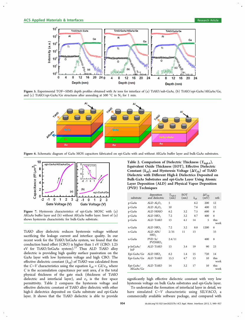
TiAlO alloy dielectric reduces hysteresis voltage withoutsacrificing the leakage current and interface quality. In ourrecent work for the TiAlO/InGaAs system, we found that theconduction band offset (CBO) is higher than 1 eV (CBO: 1.25eV for TiAlO/InGaAs system).23 Thus ALD TiAlO alloydielectric is providing high quality surface passivation on theGaAs layer with low hysteresis voltage and high CBO. Theeffective dielectric constant (keff) of TiAlO was calculated fromthe C−V characteristics using the equation keff = Cd/ε0, whereC is the accumulation capacitance per unit area, d is the totalphysical thickness of the gate stack (thickness of TiAlOdielectric and interfacial layer), and ε0 is the free spacepermittivity. Table 2 compares the hysteresis voltage andeffective dielectric constant of TiAlO alloy dielectric with otherhigh-k dielectrics deposited on GaAs substrate and epi-GaAslayer. It shows that the TiAlO dielectric is able to provide
significantly high effective dielectric constant with very lowhysteresis voltage on bulk GaAs substrates and epi-GaAs layer.To understand the formation of interfacial layer in detail, we
have simulated C−V characteristic using SILVACO, acommercially available software package, and compared with
Figure 5. Experimental TOF−SIMS depth profiles obtained with Ar ions for interface of (a) TiAlO/sub-GaAs, (b) TiAlO/epi-GaAs/AlGaAs/Ge,and (c) TiAlO/epi-GaAs/Ge structures after annealing at 500 °C in N2 for 1 min.
Figure 6. Schematic diagram of GaAs MOS capacitors fabricated on epi-GaAs with and without AlGaAs buffer layer and bulk-GaAs substrates.
Figure 7. Hysteresis characteristics of epi-GaAs MOSC with (a)AlGaAs buffer layer and (b) without AlGaAs buffer layer. Inset of (a)shows hysteresis characteristic for bulk-GaAs substrate.
Table 2. Comparison of Dielectric Thickness (Thigh‑k),Equivalent Oxide Thickness (EOT), Effective DielectricConstant (keff), and Hysteresis Voltage (ΔVFB) of TiAlODielectric with Different High-k Dielectrics Deposited onBulk-GaAs Substrates and epi-GaAs Layer Using AtomicLayer Deposition (ALD) and Physical Vapor Deposition(PVD) Techniques
substratedeposition
and dielectricThigh‑k(nm)
EOT(nm) keff
ΔVFB(mV) refs
p-GaAs ALD Al2O3 5 6.2 200 12p-GaAs ALD Al2O3 10 7.6 400 12p-GaAs ALD HfAlO 6.2 3.2 7.5 600 6p-GaAs ALD HfO2 7.2 3.2 8.7 400 6p-GaAs ALD TiAlO 13 4.1 14 5 this
workn-GaAs ALD HfO2 7.2 3.2 8.8 1200 6n-GaAs ALD AlN/
HfO2
2/35 11 13 33
n-GaAs PVD Si/PVDHfO2
2.4/11 400 8
p-InGaAs/InP
ALD TiAlO 13 3.4 19 90 23
Epi-GaAs/Ge ALD HfO2 6.2 1.4 15 720 14Epi-GaAs/Ge ALD TiAlO 15.3 4.7 13 10 this
workEpi-GaAs/AlGaAs/Ge
ALD TiAlO 14 3.2 17 10 thiswork
ACS Applied Materials & Interfaces Research Article
dx.doi.org/10.1021/am302537b | ACS Appl. Mater. Interfaces 2013, 5, 949−957954
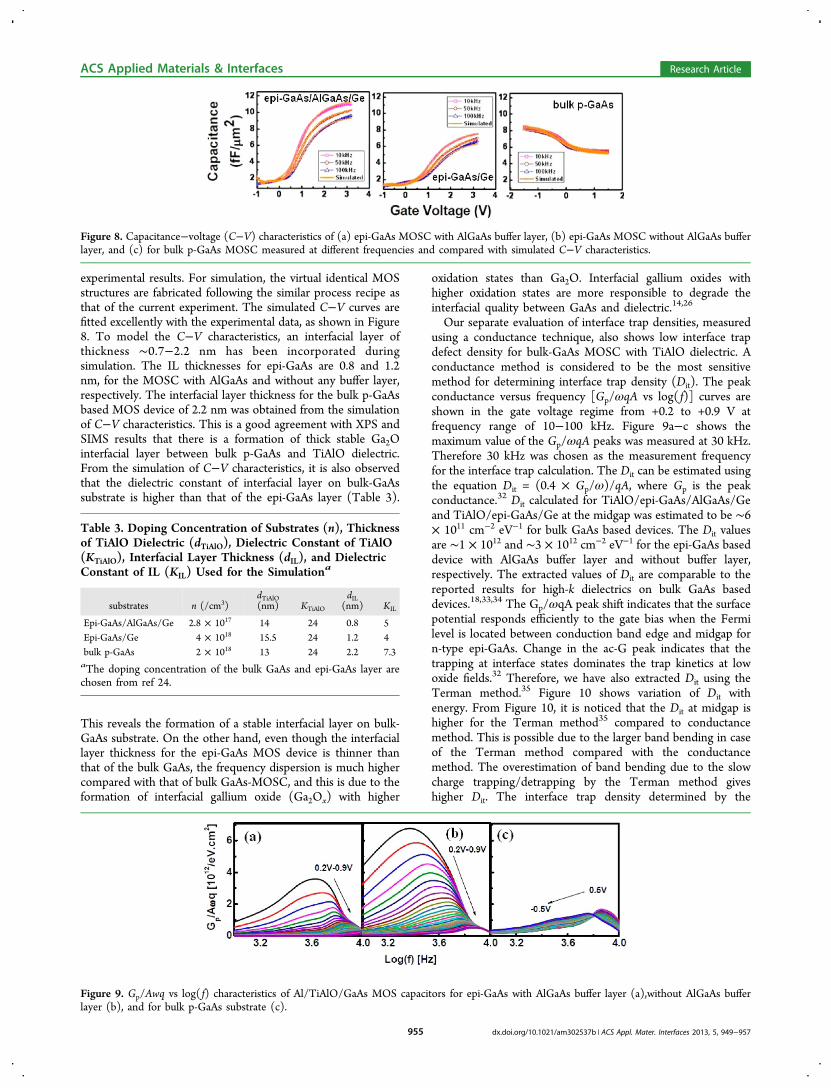
experimental results. For simulation, the virtual identical MOSstructures are fabricated following the similar process recipe asthat of the current experiment. The simulated C−V curves arefitted excellently with the experimental data, as shown in Figure8. To model the C−V characteristics, an interfacial layer ofthickness ∼0.7−2.2 nm has been incorporated duringsimulation. The IL thicknesses for epi-GaAs are 0.8 and 1.2nm, for the MOSC with AlGaAs and without any buffer layer,respectively. The interfacial layer thickness for the bulk p-GaAsbased MOS device of 2.2 nm was obtained from the simulationof C−V characteristics. This is a good agreement with XPS andSIMS results that there is a formation of thick stable Ga2Ointerfacial layer between bulk p-GaAs and TiAlO dielectric.From the simulation of C−V characteristics, it is also observedthat the dielectric constant of interfacial layer on bulk-GaAssubstrate is higher than that of the epi-GaAs layer (Table 3).
This reveals the formation of a stable interfacial layer on bulk-GaAs substrate. On the other hand, even though the interfaciallayer thickness for the epi-GaAs MOS device is thinner thanthat of the bulk GaAs, the frequency dispersion is much highercompared with that of bulk GaAs-MOSC, and this is due to theformation of interfacial gallium oxide (Ga2Ox) with higher
oxidation states than Ga2O. Interfacial gallium oxides withhigher oxidation states are more responsible to degrade theinterfacial quality between GaAs and dielectric.14,26
Our separate evaluation of interface trap densities, measuredusing a conductance technique, also shows low interface trapdefect density for bulk-GaAs MOSC with TiAlO dielectric. Aconductance method is considered to be the most sensitivemethod for determining interface trap density (Dit). The peakconductance versus frequency [Gp/ωqA vs log( f)] curves areshown in the gate voltage regime from +0.2 to +0.9 V atfrequency range of 10−100 kHz. Figure 9a−c shows themaximum value of the Gp/ωqA peaks was measured at 30 kHz.Therefore 30 kHz was chosen as the measurement frequencyfor the interface trap calculation. The Dit can be estimated usingthe equation Dit = (0.4 × Gp/ω)/qA, where Gp is the peakconductance.32 Dit calculated for TiAlO/epi-GaAs/AlGaAs/Geand TiAlO/epi-GaAs/Ge at the midgap was estimated to be ∼6× 1011 cm−2 eV−1 for bulk GaAs based devices. The Dit valuesare ∼1 × 10¹² and ∼3 × 1012 cm−2 eV−1 for the epi-GaAs baseddevice with AlGaAs buffer layer and without buffer layer,respectively. The extracted values of Dit are comparable to thereported results for high-k dielectrics on bulk GaAs baseddevices.18,33,34 The Gp/ωqA peak shift indicates that the surfacepotential responds efficiently to the gate bias when the Fermilevel is located between conduction band edge and midgap forn-type epi-GaAs. Change in the ac-G peak indicates that thetrapping at interface states dominates the trap kinetics at lowoxide fields.32 Therefore, we have also extracted Dit using theTerman method.35 Figure 10 shows variation of Dit withenergy. From Figure 10, it is noticed that the Dit at midgap ishigher for the Terman method35 compared to conductancemethod. This is possible due to the larger band bending in caseof the Terman method compared with the conductancemethod. The overestimation of band bending due to the slowcharge trapping/detrapping by the Terman method giveshigher Dit. The interface trap density determined by the
Figure 8. Capacitance−voltage (C−V) characteristics of (a) epi-GaAs MOSC with AlGaAs buffer layer, (b) epi-GaAs MOSC without AlGaAs bufferlayer, and (c) for bulk p-GaAs MOSC measured at different frequencies and compared with simulated C−V characteristics.
Table 3. Doping Concentration of Substrates (n), Thicknessof TiAlO Dielectric (dTiAlO), Dielectric Constant of TiAlO(KTiAlO), Interfacial Layer Thickness (dIL), and DielectricConstant of IL (KIL) Used for the Simulationa
substrates n (/cm3)dTiAlO(nm) KTiAlO
dIL(nm) KIL
Epi-GaAs/AlGaAs/Ge 2.8 × 10¹⁷ 14 24 0.8 5Epi-GaAs/Ge 4 × 10¹⁸ 15.5 24 1.2 4bulk p-GaAs 2 × 10¹⁸ 13 24 2.2 7.3aThe doping concentration of the bulk GaAs and epi-GaAs layer arechosen from ref 24.
Figure 9. Gp/Awq vs log( f) characteristics of Al/TiAlO/GaAs MOS capacitors for epi-GaAs with AlGaAs buffer layer (a),without AlGaAs bufferlayer (b), and for bulk p-GaAs substrate (c).
ACS Applied Materials & Interfaces Research Article
dx.doi.org/10.1021/am302537b | ACS Appl. Mater. Interfaces 2013, 5, 949−957955

conductance method only deals with fast interface traps withshort response times. However, for the Terman method, bothfast and slow traps are taken into consideration, which giveshigher value compared with conductance method.32
Current−voltage (I−V) characteristics were performed onGaAs MOS capacitors to evaluate the TiAlO gate dielectricquality on the GaAs surface. The leakage current analysis showsa breakdown field of ∼3.3 MV/cm for TiAlO dielectricdeposited on the bulk GaAs substrate and epi-GaAs layer. Theleakage current density shown in Figure 11 is ∼5 × 10⁻⁴ A/cm2
at Vfb + V with an EOT of ∼3.2 nm for epi-GaAs with AlGaAsbuffer layers. The leakage current is slightly high for an EOT of3.2 nm. This is due to the lower band gap of the TiAlOdielectric.23 The leakage current can be improved further byoptimizing Ti concentration in the TiAlO dielectric, since thepresence of Ti in Al2O3 decreases the band gap of the material.The conduction mechanism of the leakage current is similar tothe Fowler−Nordheim (F−N) tunneling characteristics. F−Ntunneling plot was performed as shown in the inset of Figure11. A straight line was observed, which indicates the presence ofan F−N tunneling phenomenon. Since F−N tunnelingconduction requires sufficient band offsets and a low densityof oxide traps in the dielectric, the presence of the F−Ntunneling phenomenon reveals the high quality TiAlOdielectric on epi-GaAs and bulk-GaAs with sufficient band gap.
■ CONCLUSIONSurface passivation of bulk-GaAs and epi-GaAs layer with ALDTiAlO dielectric is demonstrated to yield a high quality
interface between high-k dielectric and GaAs layer. The ALDTiAlO dielectric acts as an effective barrier to suppress the out-diffusion of elemental Ga and As into the dielectric. The ALDTiAlO eliminates formation of arsenic oxide completely fromthe GaAs surface. The stable Ga2O interfacial layer was formedon the bulk-GaAs surface. Excellent electrical properties withlow hysteresis voltage (5 mV) and interface defects (6 × 10¹¹
eV−1 cm−2) were observed for bulk-GaAs MOS capacitors. Ithas been also demonstrated that the TiAlO dielectric is apromising candidate for epi-GaAs based devices. By introduc-tion of the thin AlGaAs buffer layer between epi-GaAs and Gesubstrates, it is possible to improve the surface roughness ofTiAlO/epi-GaAs gate stack and uniformity of the films, out-diffusion of elemental Ga into the dielectric, and interfacequality between epi-GaAs and TiAlO dielectric further. Theelectrical characteristics of epi-GaAs MOSC with AlGaAs bufferlayer shows higher accumulation capacitance, lower fixed oxidecharge, and leakage current compared with epi-GaAs gate stackwithout buffer layer. The leakage current conductionmechanism shows the presence of F−N tunneling for theTiAlO dielectric with epi-GaAs and bulk-GaAs substrates. Theresults suggest that the high quality gate dielectric stacks onbulk-GaAs substrates and epi-GaAs layers with AlGaAs bufferlayer can pave the way toward the next generation III−V/Sibased high speed transistors.
■ AUTHOR INFORMATIONCorresponding Author*Corresponding author: G K Dalapati: [email protected] and D Z Chi: [email protected].
NotesThe authors declare no competing financial interest.
■ REFERENCES(1) Ko, H.; Takei, K.; Kapadia, R.; Chuang, S.; Fang, H.; Leu, P. W.;Ganapathi, K.; Plis, E.; Kim, H. S.; Chen, S. Y.; Madsen, M.; Ford, A.C.; Chueh, Y. L.; Krishna, S.; Salahuddin, S.; Javey, A. Nature 2010,468, 286−289.(2) Del Alamo, J. A. Nature 2011, 479, 317−323.(3) Suthram, S.; Sun, Y.; Majhi, P.; Ok, I.; Kim, H.; Harris, H. R.;Goel, N.; Parthasarathy, S.; Koehler, T.; Acosta, T. VLSI Symp. Tech.Dig. 2008, 182−183.(4) Passlack, M.; Zurcher, P.; Rajagopalan, K.; Droopad, R.;Abrokwah, J.; Tutt, T.; Park, Y. B.; Johnson, E.; Hartin, O.;Zlotnicka, A. IEDM Tech. Dig. 2007, 621−624.(5) Liu, H.; Wang, T.; Jiang, Q.; Hogg, R.; Tutu, F.; Pozzi, F.; Seeds,A. Nat. Photon. 2011, 5, 416−419.(6) Dalapati, G. K.; Tong, Y.; Loh, W. Y.; Mun, H. K.; Cho, B. J.IEEE Trans. Electron Devices 2007, 54, 1831−1837.(7) Dalapati, G. K.; Tong, Y.; Loh, W. Y.; Mun, H. K.; Cho, B. J.Appl. Phys. Lett. 2007, 90, 183510−1−183510−3.(8) Ok, I.; Kim, H.; Zhang, M.; Kang, C. Y.; Rhee, S. J.; Choi, C.;Krishnan, S. A.; Lee, T.; Zhu, F.; Thareja, G.; Lee, J. C. IEEE ElectronDevice Lett. 2006, 27, 145−147.(9) Hong, M.; Kwo, J.; Kortan, A. R.; Mannaerts, J. P.; Sergent, A. M.Science 1999, 283, 1897−1900.(10) Dalapati, G. K.; Sridhara, A.; Wong, A. S. W.; Chia, C. K.; Lee, S.J.; Chi, D. Z. J. Appl. Phys. 2008, 103, 034508-1−034508-5.(11) Frank, M. M.; Wilk, G. D.; Starodub, D.; Gustafsson, T.;Garfunkel, E.; Chabal, Y. J. Appl. Phys. Lett. 2005, 86, 152904-1−152904-3.(12) Xuan, Y.; Lin, H. C.; Ye, P. D. IEEE Trans. Electron Devices2007, 54, 1811−1817.(13) Hackley, J. C.; Demaree, J. D.; Gougousi, T. Appl. Phys. Lett.2008, 92, 162902-1−162902-3.
Figure 10. Dit spectra with energy for epi-GaAs MOSC and bulk-GaAsMOSC. Dit was calculated using the Terman method.
Figure 11. Leakage current density−voltage characteristics for ∼14 nmTiAlO film on epi-GaAs as well as bulk GaAs substrate. The insetshows F−N fitting of leakage current for different gate stacks.
ACS Applied Materials & Interfaces Research Article
dx.doi.org/10.1021/am302537b | ACS Appl. Mater. Interfaces 2013, 5, 949−957956

(14) Dalapati, G. K.; Kumar, M. K.; Chia, C. K.; Gao, H.; Wang, B.Z.; Wong, A. S. W.; Kumar, A.; Chiam, S. Y.; Pan, J. S.; Chi, D. Z. J.Electrochem. Soc. 2010, 157, H825−H831.(15) Dalapati, G. K.; Wong, T. K. S.; Li, Y.; Chia, C. K.; Das, A.;Mahata, C.; Gao, H.; Chattopadhyay, S.; Kumar, M. K.; Seng, H. L.;Maiti, C. K.; Chi, D. Z. Nanoscale Res. Lett. 2012, 7 (99), 1−8.(16) Dalapati, G. K.; Chia, C. K.; Mahata; Das, T.; Maiti, C. K.;Kumar, M. K.; Gao, H.; Chiam, S. Y.; Tan, C. C.; Chua, C. T.; Cheng,Y. B.; Chia, D. Z. Electrochem. Solid-State Lett. 2011, 14, G52−G55.(17) Chia, C. K.; Dalapati, G. K.; Chai, Y.; Lu, S. L.; He, W.; Dong, J.R.; Seng, D. H. L.; Hui, H. K.; Wong, A. S. W.; Lau, A. J. Y.; Cheng, Y.B.; Chi, D. Z.; Zhu, Z.; Yeo, Y. C.; Xu, Z.; Yoon, S. F. J. Appl. Phys.2011, 109, 066106−066109.(18) Dalapati, G. K.; Chattopadhyay, S.; Kwa, K. S. K.; Olsen, S. H.;Tsang, Y. L.; Agaiby, R.; Dobrosz, P.; Bull, S. J.; O’Neill, A. G. IEEETrans. Electron Devices 2006, 53, 1142−1152.(19) Shahrjerdi, D.; G.-Gutierrez, D. I.; Tutuc, E.; Banerjee, S. K.Appl. Phys. Lett. 2008, 92, 223501−1−223501−3.(20) Auciello, O.; Fan, W.; Kabius, B.; Saha, S.; Carlisle, J. A.; Chang,R. P. H.; Lopez, C.; Irene, E. A.; Baragiola, R. A. Appl. Phys. Lett. 2005,86, 042904-1−042904-3.(21) Kim, S. K.; Choi, G.-J.; Lee, S. Y.; Seo, M.; Lee, S. W.; Han, J.H.; Ahn, H. S.; Han, S.; Hwang, C. S. Adv. Mater. 2008, 20, 1429−1435.(22) Song, X.; Takoudis, C. G. J. Electrochem. Soc. 2007, 154, G177−G182.(23) Mahata, C.; Mallik, S.; Das, T.; Maiti, C. K.; Dalapati, G. K.;Tan, C. C.; Chia, C. K.; Gao, H.; Kumar, M. K.; Chiam, S. Y.; Tan, H.R.; Seng, H. L.; Chi, D. Z.; Miranda, E. Appl. Phys. Lett. 2012, 100,062905-1−062905-4.(24) Dalapati, G. K.; Chia, C. K.; Mahata, C.; Krishnamoorthy, S.;Tan, C. C.; Tan, H. R.; Maiti, C. K.; Chi, D. IEEE Trans. ElectronDevices 2013, 60, 192−199.(25) Kim, S. K.; Hoffmann-Eifert, S.; Reiners, M.; Waser, R. J.Electrochem. Soc. 2011, 158, D6−D9.(26) Hinkle, C. L.; Milojevic, M.; Brennan, B.; Sonnet, A. M.;Aguirre-Tostado, F. S.; Hughes, G. J.; Vogel, E. M.; Wallace, R. M.Appl. Phys. Lett. 2009, 94, 162101−1162101−3.(27) Surdu-Bob, C. C.; Saied, S. O.; Sullivan, J. L. Appl. Surf. Sci.2001, 183, 126−136.(28) Vilar, M. R.; Beghdadi, J. E.; Debontridder, F.; Artzi, R.;Naaman, R.; Ferraria, A. M.; Botelho do Rego, A. M. Surf. InterfaceAnal. 2005, 37, 673−682.(29) Geppert, I.; Eizenberg, M.; Ali, A.; Datta, S. Appl. Phys. Lett.2010, 97, 162109.(30) Hinkle, C. L.; Sonnet, A. M.; Vogel, E. M.; McDonnell, S.;Hughes, G. J.; Milojevic, M.; Lee, B.; Aguirre-Tostado, F. S.; Choi, K.j.; Kim, H. C.; Kim, J.; Wallace, R. M. Appl. Phys. Lett. 2008, 92,071901.(31) Robertson, J.; Falabretti, B. J. Appl. Phys. 2006, 100, 014111.(32) Engel-Herbert, R.; Hwang, Y.; Stemmer, S. J. Appl. Phy. 2010,108, 124101.(33) Jussila, H.; Mattila, P.; Oksanen, J.; Perros, A.; Riikonen, J.;Bosund, M.; Varpula, A.; Huhtio, T.; Lipsanen, H.; Sopanen, M. Appl.Phys. Lett. 2012, 100, 071606.(34) El Kazzi, M.; Czornomaz, L.; Webb, D. J.; Rossel, C.; Caimi, D.;Siegwart, H.; Fompeyrine, J.; Marchiori, C. Appl. Phys. Lett. 2011, 99,052102.(35) Terman, L. M. Solid-State Electron. 1962, 5, 285.
ACS Applied Materials & Interfaces Research Article
dx.doi.org/10.1021/am302537b | ACS Appl. Mater. Interfaces 2013, 5, 949−957957