distributed by: national technical information service … · w.dstiummov statement w 40* a"~...
TRANSCRIPT

AD-AO09 780
NEW PASSIVATION METHODS FOR GaAs
H. L. Hartnagel, et al
Newcastle-upon-Tyne University
Prepared for:
Army Research and Development Group(Europe)
January 1975
DISTRIBUTED BY:
National Technical Information ServiceU. S. DEPARTMENT OF COMMERCE

UNCLASSIFIED "6'' SECuRITY CLASWMCA'1ON OF TI41S PAGE (Iben Date Palwod) 4 n)/ /
REPORT DOCUMENTATION PAGE W- aa LM ORK1APGAT =0901 GOVT ACCESON NO. RCIPSEN S CATALOG NUM1eo
_____ _____ _____ R8D 2004i. TITLg few &A9 a. TYPE or REPORT & PERIOD COVKRED
Final Technical ReportNew Passivation Methodts for GaAs 1 Jan - 31 Dec 1974
6. P"FORMING ORg. REPORT UMmeR
t I OVIRM B. CONTRACT ON GRANT MUNGIEWS)
H.L. Hartnagel, R. Singh, DAJA73-74-C-1703H. Hasegawa, and I.E. Forward
s, p1.ERPOMI OGANIZATION ''. .A; 0'UGlma Tpjauwms', TAEDepartment of Electrical and 611 -02A-D6l lT02B31E
Electronic Engineering 00-444University of.Newcastle-upon-Tyne, U.K, 00-444
11. C"ONOLLIN@ OFFICC NAME1 AND A0011138 It. REPORT OATK
U.S. Aray" RD Group (Europe) January 197SBox 1S, FPO New York 09S10 i. U iorPi
W.UTopv GRUISCW "01E a '1A03ESSr41 a4ll bum G~j&V 00"e) 15. SECURJTY CLASSL (Of SWO #",No
UNCLASSIFIED
I f6YS03TIOut STATUMENY (.E . La.... ifO,
•ApprOved for public release; distribution unlimited-
W.DSTIummov STATEMENT W 40* a"~ &NOW" In* Al.i of on~I AV R'i
WS SVPPfteUETARY NOTES
WIS. KY WORMS (Caluie", i ff -I*.W7O u iF
Passivation, Surface passivation, GaAs, Anodization,Native oxide Al Z 0 3, MOS devices, Interface states,Solid state materials.
,AYRAC? em - 'in -, - -D*,dU, Sp a*.. .. b..j
The fabrication of high-quality oxides on GaAs with goodelectrical interface properties was investigated, Severalplimary and subsidiary approaches were explored. The bestr sults were obtained with a new anodization scheme based onas aqueous solution of tartaric or citric acid with glycol,aid a subsequent annealing at 250*C. This scheme is suitablefor both GaAs and At. In view of increased corrosion Cont/...
Do I W3 iTI ii O I o is OOLETt
39aJSTY CLASSIFICATION OP TWOS PAGE (Wh.W 0.
-rA

UNCLASSIFIEDSECUNTY CLASSIFICATIOM OF THIS PAOE(We at olus e4
20. Abstract Cont'd....
resistance of the resulting oxides if some amount of At isincluded, and in view of an optimization of interface latticematching, semi-insulating GaAtAs was grown by sliding-boatliquid-phase epitaxy prior to anodization. A new method ofdepositing pure AL203 by slow evaporation of AL through an02 atmosphere of S x 10' tcrr also gave encouraging resultswhich could be understood by the fact that this method isakin to that of molecular-beam epitaxy. The best electricalinterface prope ties obtained (interface state density about101 cm-2 (eV)-, vanishing capacitance hysteresis versusbias voltage, no frequency dispersion of capacitance etc.)make the results very useful for anti-corrosion passivationof optical devices and for MOS device applications.
J
iSCUJUTY C ASS FICATION OF THIS PA668%M 00e M094
.,-..A .

NEW PASSIVATION METHODS FOR GaAo
FINAL TECHNICAL REPORT
BY
* H.L. HARTNAGELR. SINGHH. HASEGAWASK.E. FORWARD
JANUARY1975
EUROPEAN RESEARCH OFFICE,United States Army,
London NW1 5TH, England,
Contract Number DAJA73-74-C 17Q3
UNIVERSITY OF NE14CASTLE UPON TYNE,Department of Electrica.l and Electronic Eneineering,
Newcastle upon Tyne, NEl 7RU.
Approved for public release; distribution unlimited.
II6
I I I 1- -I 1 1 1 F I -tali . . . .. J ...

TABLE OF CONTENTS,
ABSTRACT 1
CHAPTER I Introduction 2
CHAPTER 2 Deposition of Ala20%on GaA by 7
Evaporation of Al. through 02
Gas
Introduction 7
A12 03 Deposition 7
Electrical Measurements of the 8
Metal - Oxide - GaAs Structure
CHAPTER 3 Passivation Scheme utilizing GaAlAs 12
LPN Layer
Description of Passivation Schemne 12
using LPE Growth
Epitaxial Growth of Semi-insulating 15
GaA1As Layer by LPE Technique /
CHAPTER 4 Anodic Oxidation of GaAs 23
Introduction 23
Anodic Oxidation of GaAs using 25
the New Electrolyte
Dielectric and Interface Properties 29
of the Anodic Oxide II.
A New Double-Oxide Structure using 33
Anodization Technique
CHAPTER 5 Assessment of Interface Properties 39
Introduction 39C-V Plotting System 39
Application 39
Discussion of C-V Plotter 40
CHAPTER 6 Additional Passivation Schemes investigated .41
Introduction 41
Spin-on Si02 films 41
Anodization of Al 42
e-gunn evaporation of A12 03 43
SNOW

PEMe
Passivation with AS203 44
Native Oxidation of GaAs using 44
an aqueous solut ion of NaOCL
Passivation with semi-insulating 45
GaAs and GaAtAs layers produced byproton bombardment
MiPER 7 Fabrication of Devices 48
GaAs MOSFET 48
Fabrication 48
Discussion of M08 fabrication 49
Charge Coupled Device (CCD) 50
APPEND ICES
" IAn Automatic C-V Plotter", Copy of
a paper submitted to Journal of
Physics B., 1975.
II List of Publications on the results
obtained under this Grant.

1i
Abstract
The fabrication of high-quality oxides on GaAs with
good electrical interface properties was investigated.
Several primary and subsidiary approaches were explored,
The Lest results were obtained with a new anodization
schem~e bnsed on an aqueous solution of tartaric or citric
acid with glycol, and a subsequent annealing at 2500 C.
This scherie is suitable for both GaAs and AP. In view
of increased corrosion resistance of the resulting oxides
if 'me a:aount of Apis included, and in view of an
optimization of interface lattice matching, semi-
insulating GaAYAs was grownby sliding-boat liquid -
phase epitaxy prior to anodization. A new method of
depositing pure Av203 by slow evaporation of Ak through
ar: 2 atmosphere of 5 x - torr also gtve encouraging
results which could be understood by the fact that this
method is akin to that of molecular-beam epitaxy.
The best electrical interface propertiez obtained
(interface state density about 10I on,- 2 (eV)- ,
vpnishinG capacitance hycterezis versus bias volta7no frequency dispersion o' ca -pacitance etc.) make theresults very useful for anti-corrosion passivation of
optical devices and for MOS device -pplizrtions.
aI (Unclassificd)

2
CHAPTER 1 _
INTRODUCTION
Whereas the passivation of Si is well developed,
there are serious difficulties associated with surface
passivation of GaAs and other compound semiconductors.
These are primarily caused by the high vapour pressure of
one of the components such as As so that it is impossible
to apply easily similarly high temperatures as usually done
for the production of Si02. Non-native oxides, which can
be deposited at lower temperatures, exhibit poor adhesion,
high interface-state densities and increased lateral
diffusion of impurities along the semiconductor-oxide
interface which is particularly serious in connection with
diffusion masking applications.
We felt that a promising exception for GaAs would
be a slow deposition of AL203 together with some At,
particularly at the beginning of the deposition process.
At forms with GaAs a ternary compound with a lattice constant
which is very close to that of GaAs. Several schemes were
attempted such as evaporation of AZ203 from a W boat at very
high temperatures* and electron-beam sputtering without any
useful results. However, one of these exploratory efforts
gave encouraging results which lead us to embark on a more
systematic study of this metbod. This was slow evaporation
of At through 02 at a pressure of 5 . 10- 4 torr - a method
which is rather related to thrt of molecular-beam epitaxy.
These studies were then performed by R. Singh** and
resulted in MO0 capat1PtM with an already useful reduction
in interface state densities. This work is being continued
by a new comer to our laboratories, A. El-Safti.
Another new approach which was pursued by H. Hase gY***
is to try to passivate the semicondictor with an insulating
*These early experiments were undertaken here primarily byour colleague J. T. Kennair.
**On leave from the Department of Electrical Engineering,University of Rookee, India.
***On leave from the Department of Electri'1al EngineeringHokkaido University, Sapporo, Japan.

3
crystalline structure with a perfect lattice match to the
semiconductor rather than the usual scheme of growing
a non-crystalline amorphous structure on the semiconductor,
in order to obtain, in particular, very good interface
properties with low slow and fast state densities. Detailed
considerations led to the composite scheme of (1) growth of
a semi-insulating GaAkAs layer and (2) partial oxidation of
the grown layer by an anodization technique.
However, a series of efforts showed that it is not
possible to produce semi-insulating liquid epitaxy layers
with Cr doping, as all the layers produced turned out to
be not only semiconducting (without any intentional doping,
our liquid epitaxy system gives semiconducting GaAs with
n a 1015 cm- 3 ), but highly conducting. This is an
indication that Cr could probably then be incorporated as
a shallow donor impurity. On the other hand, sufficiently
high resistivities were generated with Fe doping. As a by-
product, an,.S-type instability was found with structures
made with metal-eemi-insulating GaAths - n GaAs sandwiches. IAn extensive effort was also made to find a
suitable anodizing agent of the GaAZAs layer in connection
with the proposed composite approach.
In the light of our previous experience, and taking
into account all the results reported by other laboratories,
including the results reported by B. Schwartz and co-workers1
on anodization in H202 , we were'able to develop, on the basis
of various ideas we had, an electrolyte based on an aqueous
solution of tartaric or citric acid. By adding a large
amount of glycol to this solution, the resulting oxides of
GaAXAs became layers of high quality.
More importantly, we have found thate new
electrolyte can produce the native oxide of GaAs with superior
dielectric properties. Therefore, detailed growth data of
such an oxide has been established..
An automatic C-V measurement system has been

4
developed by K.E. Forward* and extensive C-V studies ofMOS capacitors, made with such a native oxide, have been
carried out including annealing effect.
When the oxide layers, produced by our new
electrolyte, were annealed at about 3000C, an impressive
improvement of the electrical interface properties was
obtained, namely an interface state density of aboutlO11cm-2 (eV)-1 , a disappearance of the low-frequency
dispersion of the accumulated capacitance previously
always observed, and a large reduction of the capacitance
bias voltage hysteresis, i.e. a removal of the majority ofprobable traps in the oxide near the interface. These
results are indeed very promising so we decided to
fabricate a GaAs MOS transistor in order to measure the
surface mobility and other properties of such devices whichshould have important logic - circuit applications becauseof such properties as high carrier velocities and mobilities
and short excess-carrier life times due to direct-gap
transitions of GaAs. This has also been undertaken so farprimarily by K.E. Forward and H. Hasegawa. They have recentlybeen joined by a new postgraduate student, B, BayrAktaroglu,
who has also loohed into the possibility of producing a GaAs
CCD in order to study surface properties.
It has also been found that our native oxide of
GaAs has poor chemical and thermal stabilities as comparedwith SiO2. Therefore, various efforts have been initiated
to improve these properties without losing the favourableinterface properties.
It was establishud that At could be oxidised by ournew anodization process. Ak203 is resistant to most etchants
and produces therefore a layer of improved long-time stability.
Even small traces of AX203 in native oxide of GaAs improves
*On leave from the Department of Electrical Engineeringo
Monash University, Victoria, Australia.

5
the etch-resistance of the oxide layer. We therefore
evaporated At first onto GaAs and then anodized the whole
At and some part of the GaAs underneath it. The oxide
layers thus formed were indeed very stable.
In order to incorporate At with a uniform level
into the oxide, a layer of GaAZAs was grown by liquid-phase
epitaxy on GaAs and subsequently ionized. This epitaxyapproach enables one also to a certain extent (depending
on the solubility data) to incorporate other elements into
the oxide which might have beneficial effects such as anI increased thermal and etch-stability of the glassy structureand reduced impurity-diffusion across the oxide layer
produced in view of working applicathns.
Finally, we are continuously searching for
other solutions to oxidation of GaAs. An interesting
possibility of producing As2 03 on the (111) As surface of
GaAs bj -.oncentrated HNO3 was studied by B. Weiss.
This report describes therefore the results of
evaporation through 02 gas in Chapter 2, the liquid-epitaxy
work on GaAkAs in Chapter 3, the new-electrolyte data and
C-V data of MOS capacitators in Chapter 4, the electronic
circuit developments undertaken for a speedy assessment
of the electrical interface properties in Chapter 5.
Other miscellaneous efforts for oxidation which have been
tried are given in Chapter 6, which includes the use of
a spin-on Si0 2 film, an anodized AL 2 03 film, an electron-gun
deposited AZ 2 03 film, native oxide of GaAs produced by a
NaOCt solution, semi-insulating GaAs and GaAZAs produced
by proton bombardment and an As 2 03 layer from a HNO 3
solution. Finally, the work undertaken so far on
MOSFET and CCD struetuXes is presented in Chapter 7.
As appendices, we give the cc.uit detail of the C-V
data and list of papers submitted for public-atjon..

REFEREITCES
1. Logan, R.A., Schwartz, B., Sunclburg, W.J.
"The anodic oxidation of GaAs in aqueous
H202 solution". J. Electrochen. Suc.
120, p.1385, (1973).
CHX"PTE. 2
DEPO'SITION OF A.2-1 3~ onl _GaAs LB EVAPO iAT10ii OF A THZOUGHI 0 2 GAS
.1 7_11TAODUCTION
z t " _ describedt here hc-.. 2~ 203 is _ cpcA-d on G_-As .y
7,L!;1c! evaporation thrcLja a,, low pressurz- of oxygen. This*reh:- is si.ilar to ha cC.' oe~a-o~ opitaxy ()
A seacurernent of the interfa.co state dcnsity shows that
th-*s I's reduced, as co-.ip-rzed to the valzizs obtained w'ith
othe r co!.mon methods of covarn& Gas by an o; i-do. It
ca-n therefore boecxpecte' t-i.t further reductions can be
achievedl by exploring thI.s mcet -od more dGy
0,--r interf~cc state dc~itys deteriLie,: across
oa rt of the ena3rfr ga-p noir the fla)tband conlition.
_,s-t indicate that t.1 ---- ;ity peakIs near the
conliuctfon band eclgo mr ::lrrann~er :-s I*n Si, but
tha, the density ---Dioa osz not vairy a;: strongly
with energy as Founc.- f c!- S-.
2,.2. A' -3fDEPOSITION
'Ie lha ve :-ianuf-cturez .,.~ on Ga As slicac (Orientation
100) Jy ovaporation of 1I . Through i lc-. 02 at-:osphere.
The 3tched. -.. d claa coltaxiaol GaAC (n-n +) sample
was E; rs supplied -vith ai Cjed ohmic contact on the 1,
substra-te face, by evaporaitl.: In-Ge-A> fllu-s rand rilleyirz
_ ydoen atiaiosphere -A 620 0 C -or I ui.The ohm'c
contact thus formnec', wao covered with! a lanyer of photoresist
to protect it duirinE etchim':,, of the epitaxia-l layer for the
devosi4t]on of A) 203 Tho etch soluto1.:n zusodwa
NH11 0Hk1 2.3 2:H 20 of tbe rat-_oc 1 :4:20. The slicews
then- ;ucunted in a, vac, ua-. :r,,poritor. An i.lun.*nacatc
mclylodenumn boat war: ch;,rgd ;ith a snllqua-ntity of'
99. 999% nure Alamin. s-ri. W hcr. the vicu.sra pres sura isth
chi-iber was redJuced to ~:trthan 101- tcrr, the boat
tormperature wis slowJly ras to ,ibout -i n; nd
Ptluriniu.. was evapor.,.tzei_ c'5:iiue 1a;
-: Shttt r. Th-iF' s: ir nci.osary i'. . r

the Aluminium by first evaporating against a shutter for a short
........ t .. Tl() to cover all freely exposed elements present
in the chamber with an Aluminium film which will avoid oxidation
and evaporation of any material other than Aluminium. Setting
the temperature then just below evaporation, oxygen was admitted
into the chamber such that the equilibrium pressure of the out-
going gases and incoming oxygen is 5 x 10- 4 torr. Five minutes
later when the Aluminium vapours were fully saturated with
oxygen, the shutter was opened and the epitaxial layer was
exposed to a slow deposition of Aluminium Oxide. The distance
between the source and the sample was more than the mean free
path of the molecules at this pressure.
Thus, oxygen present in the chamber is permitted to
react with Aluminium at the molten surface, in the vapour phase
and at the epitaxial layer surface. This feature ensures that
the layer in immediate contact with the GaAs surface is A£203
and of the same quality as the top layer. Moreover, it results
in a higher yield than that of other methods.
When the .desired thickness of around 1200 of Ak2 03 is
grown the shutter is closed anU the heater supply switched off.
The sample was then allowed to cool down, exposed to air and
placed in an oven at 1500 C for 3 hours to anneal the layer and
to complete oxidation of any not fully oxidized Aluminium near
the surface. Subsequently a metal electrode as a field plate
is deposited by evaporating Aluminium under a good vacuum.
2.3 ELECTRICAL MEASUREMENTS OF THE METAL - OXIDE -GaAs STRUCTURE
It is important to establish the charge state density
at the semiconductor - oxide interface as a function of the
energy across the energy gap, and the relevant charge-capture
time constant Tof these states. This can be obtained most
conveniently by measuring the rf conductance as a function of
angular frequency w,, from which the equivalent interface-statc
conductance G can be derived (2). The function Gp/w = f(w)pIpeaks at wT =1, where its value gives also directly the
interface state density Nss. Unfortunately, this convenient
method is only strictly possible if Nss is not a continuous
function of energy but is present at a discrete energy level
i
9
only. The more accurate method for a continuous Nss functioninvolves a rather sophisticated evaluation procedure. However,it becomes doubtful whether the more involved procedure isjustified at this stage of order-of-magnitude investigations ofGaAs oxides, because it is quite possible that these structuresshow very different phenomena from those of Si - Si02 and thata different equivalent circuit to that given by Nicollian et al(4) is valid. Therefore it was decided to undertake theconductance evaluation by assuming a quasi-single-statebehaviour. A comparison of Nss for Si 02 on GaAs gave thesame value as obtained by Adams et al (3) so that the errorproduced by our assumption seems to be negligible. Unfortunately,it is only possible to obtain peaks of Gp/w with our Boontonlectronics Direct Capacitance Bridge for conditions when theFermi level .is near to the conduction band with our n-typematerial, as the value of T is then sufficiently short for thepeaks to occur above the minimum frequency of operation for ourbridge, namely 5 kEz. Several types of GaAs slices were used.,and tested and the results were basically the same. The dataof thl.sample where results are presented below is as follows:-:.
Gas-epitaxy 0.77Qcm layer of 6p thickness and of
mobility 7000 =2 /Vsec on n+ substrate, orientation (100)thickness of A4203 layer : 12001 as determined by profilemeasurement with Dektak'profile plotter after a slow evaporationprocess of 30 min. with a distance of 18 cm between
evaporation source and sample. The insulator capacitance Ciwas. determined by fabricating an At - AL203 - At sandwich on aglass substrate by a separate evaporation process with thespisparameters as used for the oxide on GaAs, and it was found thatCi - 15pF. The interface density obtained and the chargefilling time T are shown in Fig. 2.i.
A measurement of the device, .itSnce with biasvoltage VB shows that after the app,,4Lat4on of,:a positive biasvoltage of about 2 Volt, the capacitan.acqrve, is,, shifted up- "wards by typically 0.8 pF. It can,be assumed that- this .. ,caused by some traps filled in the insulator by.t.he applicationof a positive bias voltage. It is f9und, thatjthis shiftcannot be removed by the application of a negative VB up to at
i " : - I .. . . I IHH H>H

C- 10 -
least - 3 volt, and that it is maintained over many days.
By correctiE. toc measored capacitance increase due to this
trapped insulator charg,, and by the removal of the series
connected insulator capacitance Ci, thQ spaco charge layer
capacitance Cj) is f-irad as a funrc.i n of Vb. This is shown
In Fij. 2.2. This infornation can be used to find the
approxmatk: valuet of voltage V. at the se.ienductor surface
and curresponding zcait, s have been introduced on Figures 2.1
and 2.2. The results j Pig.2.2cun b. usel to obtain the flat-
band voltage VFB by taking the flat-band capacitance of our
zater'.al, which is ClL - 59.9pF where w- used the relative
permeability for GaAs, es&12. This gives a flat-band voltage
VrB +0.5 volt, which determines the value or the negative
fixed charge near the somiconductur surface inside the insulator,
namely 6 x 10¹⁰ c,:- 2 . The above described capacitance - curve
shift of 0.8pF after the application of a positive bias voltage
can be used to deturmine the dcosity of slow traps and it is
found that they arc 0ilso about 1 x 101 0 cm-2 .
In an attempt to obtain an estimate of Ng8 for
VB < 0.7 Volt, when the conductance peaks occurred at
frequencies below thu measurvment rango cf our Boonton Bridge,
we measured carefully capacitance versus frequency for various
bias voltages. After removing the contribution of the series-
connected C1 , we obtained the capacitance Cp. If the model of
Nicollian anJ Goetzberver (4) is corrcl for our oxide
structure, Cp would nave to satisly u given frequency dependance.
i Unfortunately, our experimental findings do not fit the required
dependance and it seems likely that uiff rent types of additional
states with different charging times have to be taken into account
wbich could be relatively fast traps inside the oxide. The
corresponding tim constants could be expected to be higher than
those of the interface states bocause tbey can only be filled by
a tunnelling process with reduced probability. It appears from
the experimental data that tho equivalent circuit does not have
a series RC branch connecti-, in parallel to CD as proposed by
Nicollian lt 1 (4), but in parallcl to Cs . This could indicate
that the traps can only b,. filld via a two-step process involving
an intermediate transtcr firsit into the intcrface states.
: ... . . . ... .. l l l l i ... .. " ... .. " ......
REFERENCES
1. Ilegerns, H., Dingle, R. "Acceptor
Incorporation in, GaAs 4Grown by Mclecular-Bean
Epitaxy"l. 1st paper of Vth International
Symposium on GaAs and Rel. Comp. Deauville
France, Sept. 1974. Proceedings from Institute
of Physics, London.
2. Nicollian E.H., Goetzberger, A., "1The Si - Si2Interface-Electrical Properties as Determined by
,.,the Metal-Insulator-Silicon Condu i tanc& Technique"
Bell1--Sst, Techn. J. 46, p1055, (1967 ).
3. Adams A.C. Pruniaux, B.R, -"''GaAs Surface Film
*Eval~uation by Ellippamrtry and .'Its Effects on
Schottky Barr. or" J. Electrochem,, Soq,,
Sol..:St 84C -and Techn. 120, 1973, p40.0.
EReproduced Io
FIGURE CAPTIONS
2.1 Interface state density Nss and clxarge capture time
T-versus bias voltage VB applied to the MOB sandwich
applied and approximate semiconductor-surface
potential V. for Ak203 deposited by evaporation
of A2. through 02.
2.2 Space-charge capacitance CD versus,VB and V5
for "22 03 sandwich of Fig. 2-.1.

12
Yig. 2. 1
NiCM2 e -I 12A e
1.5 20
1.0 10
0.5 0V$NOlt
(nonlinear scale)
0.026 0.05 0.08
Q7 1.0 1.3 1.5
(linear scale)
Int'jrface state density Ns5 and charge capture
time T versus bias voltage VB applied to the KOS
sandwich and approximate semiconductor-surface
potential Vs for A1203 deposited by evaporation
of At through 02.

13
Fig. 2. "2
80-
60 --- CFB
-40 1
Vs/Volt
(nonlinear scale)
-0.41 -0.24 -0.1 0.0 0.05
-1 -0.6 0 0.5 1.0VB/VOltO (i.n scaile)
Space-charge capacitance CD versus VB
and V, for AX202 sandwich of Fig. 2.1.
14
CIL'.PTEa 3
PASSIVATION SCHEKE UTIL2IZING GaAlAs LPE LAYBE2
ItE~s ee el rccnie nw ha o(ofth.-i
3. 1 DESCRI.PTION OF PASSIVATIO11 SCHEME USING LPE GROWTH
purposes to provide a pcossiva ting layer on a semiconductor
surf~ace is to "lectro-xic-clly! passivate th~e surface, i.e.
to provide a nearly idoal. tra.s itio-. from the active semi-
condu ctin- region to apassf;V_ insulatinji region withoutintrodu-cing additional elactrcn!cally active states at the
interfnce which .,ill1 deteriorate operation and stibility of
the dovi ce. The exact phycis-l origins c- th*.csa interface
statecs have not been -oa ,et even in thc case of the
Si-SC)2 system, but it i-s rger..rally acceptead that these states
a re assGociated with some types of structu-rn'. defects at the
interface (1)(2). ThIc f:c-t ceems to sgstthat, if one
can Crcw an inoulatinE crystalline material ini an epitaxinl
s~rigle-erystal form with n coialete lattice match to tie seni-
con:d-,rcr, it will prcviri.o.; -n excellent passivation layer.
Such a scheme is an. opposite,- extremne. Th:i -,assivation as
compa -red with the usual r-tylc w;here a crystalline structure
Js trn.zsj:ermed to an amrinphi>_n glassy structure.
Clearly, the success -f such a ocho-i depends on -.he
avzilailt of the is tnLcrystal -;-t'- agood latti'ce
match to the semiconducs_-or.
'Fortanately the int-r2i asic cat-rrier concentration of GaAs
and related ternary co-mpouncs ic, low, at ten2,_porratires of usual
cievics3 operation duo tc 'ad aiergy ga-ps, cc t-hat semi-
irnsulotia' crystals co;.! e1 :f rown eit'-o-r in the usual deep-
levol compensated form --r even "undoped" formr, epitaxinlly on
Ga~s surface w~ith a jgoc.' lattice inatch.
'-hv;i other hand1 onc: o-_-n not expect tlh,
(_":c u Ilcnt :ielectric broakAoi,rn pr, portA 'JS uzl ly
f --n 'it insult. :xi- e n,,terials. The

15
current conduction and electrical breakdown phenomena in semi-
insulating GaAs are known to be well explained, at least
qualitatively, by the space-change-limited current and double
injection theories of Lampert and others (3) (4) (5).
According to the experimental results the maximum resistivity
so far obtained is of the order of 108 ohm-cm and the break-
down voltages reported in the literature (6) vary from 15V
to 150V for bulk semi-insulating materials with the thickness
of 150pm, deperding on whether the material is undoped,
oxygen doped or chromiumdoped, and on the type of contacts
used. If one also takes into account that the so-called
trap-filled-limit-voltage, which gives a rough measure for
the breakdown voltage of semi-insulating materials under
carrier injection, varies in proportion to the square of the
thickness (3), the breakdown voltage of the semi-insulating
layer with several micron meter thickness will be estimated
to be only few volts at best. This means one needs the
additional formation of an insulating layer by suitable means
on the free surface to prevent carrier injection from outside
and to improve the overall dielectric properties. Although
various oxide or nitride deposition schemes could be employed
for such a purpose because requirements for interface
properties are not so severe there, a somewhat different scheme
has been pursued in the work reported here.
It is a two-step passivation scheme utilizing the liquid
phase epitaxial growth of GaA£As layer, which consists of
(1) the formation of a thin semi-insulating GaAlAslayer on GaAs by LPE techniques
and
(2) the subsequent partial oxidation of the LPE
layer by anodization techniques.
The reasons why GaAkAs is particularly chosen are as
follows: (1) GaAXAs has a close lattice match to GaAs;
(2) GaAXAs has a wider energy band-gap and should form a
heterojunction barrier to the carriers in GaAs: (3) a more
chemically and thermally stable native oxide could be formed
on GaAXAs than on GaAs, because of the inclusion of At atoms
which have high oxygen affinity.
" ... mmmmm mmm - - ...
16
The epitaxial growth of a GaAZAs layer cii GaAs can be easily
done by liquid-phase-epi4taxy, while vapour-phase growth of
this material (7) still seems to remain at its early stage.
A horizontal sliding LPZ System developed at this laboratory
by A. C'oiquhoun has been --ased for the present work, which is
basically similar to that described by Panich; et al (8) forthe fa*bri4cation of double-iieterojunction. lascer diodes.
Unfortunately thic work reported is ctill incomplete in-
tha sen~se that it has not yet reached the stage where a full
and final assessment of the proposed passlvation structure is
possible, although each of the_ steps lending- tO the structure
has ncw c3een well establicshec. This is partly because of
the difficulty encountered in ;:rowing chromium-doped sem-
insulating GaA'YAs layers by the LPE teclinio,.e, which had not
been foreseen. Mnother reason is that the extensive effort
to find a suitable electrolIyto for anodization of GaA 'As
layers hns led to the discovery of a new electrolyte which
has been also found to Eive excellent results on GaAs and
whf-'ch has led to the work rs'norted in Chapter 4.
The next section descr z. es the deta7ils of the growth of
GaA, As semi-insulating LPE layors and nn S-l-ypa instability
observed in Fe-doped laycrs-. The details of the anodization
process will be given in Chpapter A in cc nnect%-ior. with the
native oxidation of GaAs. 0.., of the main differences between
native oxides ofA GaAs anc'- G-aAk'As is that the latter has a
higher chemical stability ns verified 6y various etching.
experiments. This is a1sc consistent w~ith the result
reportad b3y Schwartz at al (9) where the notiv3 oxide of
GaA U~s layers was prepared '.-y 'boiling_ In an arluaous H 202solution.
Although the work concerning anodic native oxide given a
great h1one to passivate GaAs in a simi2.ar simnple manner to Si,
which certainly nakes the composite approa7ch described here
less attractive, we still bDclieve that it i, .,iorthwhile to
pursue it further in future, not only because passivation by
a crystalliae structure is conceptually interesting, b3ut more
inportantly because it *;c -ld CgLve a struct-ure which is iorc
stable chemically and therrnzlly than the struacture based on
the na7t'vo oxide.

17
.2 EPITAXIAL GR(Y4TH- OF SailI-ISULATI1G GaA As LAYER 3YT72 TEC-HNIQUE.
k typical. horizontal 1idin-boat1iqc-phase-upitnxy
system a.s shown in Figuira 3.1 with a Pul-di-7fused hydroGen "low
was *5 for the experi:men-t. L. high-purity lhip'h-density
caroo'on slider was des-J_:nod and! construct--L' for the purpose.
n-type Ga. s bulk mterinls (Si-doped) with (130)
orientation were used a~s the --~rae fo hegowh
The temperature starting tha growth was in the range of
780-'-330 0C and the cooling rate of typically 1 0 C/min. was
employed. A high-precision PID temperature control system
(Eurothern) was used to produce the contro~lled temperature
variation.
The substrate size ic 3 x 6 mm 2and the growth was done
from a Ga-rich melt which is typically 600-- 1000 mg in the
total .-,eight. To prepare the melt a s-"itable amount of
unioped polycrystalline GaAs and a suita'ala amount of the
deeap level dopant were put intc Ga solutio.,n and heated up
and kept in a H 2 flow for several hours at a temperature
which is higher than the actua-l growth temperature. This
is to ensure the complete d-issolution. Then, nfter coolinj
down, a suitable amount cf At' is added tc the melt and the
substrate is loaded to th;slider to start th-, actual -rowth.
A caireful cleaninE procedlure was applied to the substrate
before putting it into tlc -rowth system whichl- includesa
series of ultrasonic cleanino in various or,:anic solvents,
a 1 Soxlet" recycling clennini_ in isopropyl 7lcohol and
boilincr in HCX solution.
To establish the J;7sic performances of the growth
system various LPE layers were produced wi.1thc-ut doping, the
melt with the "deep-level', impurities. Ga1I- AUl As LPE
layers with x being from 0 to 0.3 and with a thickness
rang-inG, from I to 30 pm were grown with reas-ona bly good
surfnce appearances. The value of x wc:s -'tormined by the
X-ray microprobe analysis a~nd the thickness of the epitaxin]l
layer was measured by dcliie-tinC the bcuncory between the
epi-layer and substrate -Kth -. potassium forricyanide
etchant. It is well kn-. rn t--.t even P rmall lattice
18i
mismatch of a few fraction o' a percent can Cive rise to the
heterojunction interface state density as high as 1012 c - 2.
Thaiefore x was restricted to the above range of 0 to 0.3 by
taking the si:mple theoretical expression for the dangling
bond density as the measure for such states -nd by limitinr
this value well below 10 11c.- (10). The conduction type
of the "undoped" GaACAs LPE layers has been found always
n-type wLth the carrier 2onceotraticn of less than 5 x 10¹⁵ c' - 3 .
The carrier concentration 's determined by the C-V measurements
on the reverse-biased Schottky diode wita a Ag or A electrode
using a 3oonton 3ridge.
As the dopants to prod.ce sei-insulating GaA As by the
deep-level compensation mechanisi, various dopants have been
tried. These include chromiucm, chromium oxide (Cr0 3 , Cr 2 O3),
gallium oxide (Ga2 03 ) and iron, and, as described in what
follows, only iron has been fcund to produce highly resistive
layers, while all the ether dopants gave rise to highly
conducting layers in the coses of both GaAs and GaAQ2,s. In
order to prevent mixingj up cf 5lifferent dopants, a thorough
cleaning procedure was appliecd to both c2 the quartz furnace
tube and slider after the experiments cn each dopant,
including slight etching by MF solution for the tube and
cleaning with aqua regia, rrolcnged boiling in water, heating
in vacuim (10- torr) uni gettering impurities by undeped
pure Ga liquid.
Zhromiunm is added to the Ga-melt in the -:orm of powder.
%cccrding to tho literature (II) chromium is attached by Ga
and _.issolves into the :;t above 600 °C. The concentration
o' tho chroiiium in the vilt WIns varied from 1% up to the
maxaumnu oC 10% by weij-ht but within this range the grown layers
of GaAs and Ga _ xA xAs (x 0.3) were foun' to be all n-type and
highly conducting with the carrier concentration being in the
range of 1016 - cm17 '&- . Although chromium is known t be
the best dopant for the grn' of semi-:tnsulatiag GaAs by the
Czochralski method. the prese- rt result indicates that this is
no longer true for the epitaxlal ,rowth of GaAs and GaA As
, t:'- LPE techniquc. Th ro c-ul-., be ,vr-l puszible
2xp1'.:)oti no fcr this i'ffcr rzt bohviour. For instance

19
(1) the segregation coefficient, k, of Cr is too small in the
case of LPE or (2) the solid-solubility of Cr is too small,
either of which can lead to the situation of an insufficient
number of Cr atoms to compensate the "residual" donors of
about 5 x 101 cm- 3 . However if (1) is the case, the
effective segregation coefficient of Cr should be at least
5 x 10⁻⁶ to explain the experimental result. This seems too
small as comparea with the published data of the segregation
coefficient of about 5 x l0-4 at the stoichiometric condition
(11) (12) (13) even if one takes account of the differencesI
of the growth conditions. In this sense,case (2) is more
probable because the solid solubility 3f heavy-metal deep-level
impurities in both Si and GaAs can take quite commonly the
value in the range of 1015 cm - 3 at the temperatures of 600 -
8000c. In fact this seems to be the case for the vapor-
phase epitaxial growth of Cr-doped semi-insulating GaAs using
chromyl chloride reported by Mizuno et al (14),where successful
growth was done only when the donor concentration of the layer
is below 5 x 1015 cm- 3 . However, for the present case, neither
of above (1) and (2) can explain the high carrier concentrations
consistently observed in the growth GaAs and GaAkAs layers.
Other possible behaviours are as follows. Although
a sufficient number of Cr atoms are present in the grown layer,
they are no longer making the usual deep acceptors but acting
either (3) as electronically inactivc impurities or (4)
actively as shallow donors. The case (3) is known to be quite
common in Czochralski bulk materials where a certain fraction
of Cr atoms are always found to stay in the crystal being
electronically inactive (11) (15). The same type of inactivity
has been also reported in the case of diffused chromium (16).
As for ,he case (4), E. Andre et al (17) has rcported that Cr
acts like a shallow donor in the LPE GaAs, although the
segregation data of k.10 - 5 obtained by them seems too small
to explain the present case.
Apparently the present result seems best explained by the
case (4) of the above with the effectivu segregation coefficient
of the order of 10- 4 , although the other possibilities cannot
still be completely ruled out.

20
Obviously the be)aviour of chromium in GaAs and GaAkAs is very
complicated and future work is necessary to explain all the
experimental facts in a self-consistent manner. To clarify
the actual position taken by tho chromium atom in the crystal
lattice seems particularly important for such a work. For
example, it seems not twounrealistic to assume that the usual
deep acceptor level is associated with the chromium atom
substitutionally put into the Ga-site which would become less
possible in the Ga-rich situation of the LPE growth.
The doping of chromium oxide was also done in the form
of powder. Two types of oxide, i.e. Cr0 3 and Cr2 03 were tried
and both failed to produce semi-insulating layers. The reason
of trying chromium oxide was based on the experimental
observation (18) that most of the good Cr-doped semi-insulating
GaAs tends to contain oxygen atoms whose number is nearly equal
to that of Cr-atoms which seemed to suggest a possible presence
of a certain type of Cr-O complex. The present result obviously
canuot rule cut such a possiiility because both the extremely
unstable and volatile nature of Cr03 and the extremely stable
nature of Cr2 03 could equally become the cause for insufficient
doping into the melt. Dopinr by up to 10 wt. % into the melt
has been tried and resulted in n-typo ccnduction with the
carrier concentration ii, the low 1016 region in both cases.
Iron was doped in the fcrm of wire into the melt in the
range of 2-7 wt. % and it has been found that such a doping can
give rise to a very highly resistive p-type epitaxial GaAZAs or
GaAs layer with the specific resistivity of the oruer of
103-104 ohm.cm which is consistent with the double deep-
acceptor levels of Fe reported in the literature (19).
The detailed electrical properties of the iron doped
LPE layers were studied further by depositing metal contacts andforming M-i-n (metl-semi-insuiator-semicnductor) diodes
which is an alogous configuration to the MOS structure.
Aluminium is used as the contact material. Thickness of
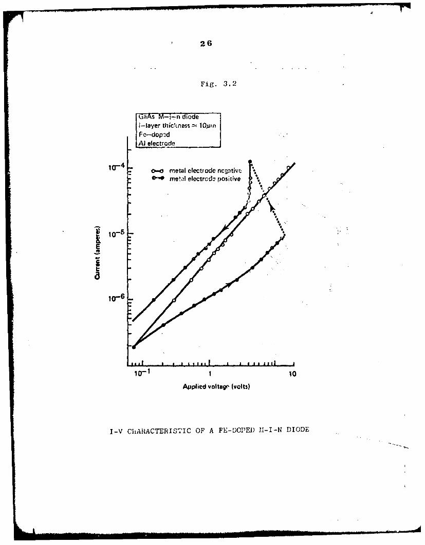
i-layer was 10 to 30Um. The current-voltage characteristic
of such a diode hts been found to show a reproducible S-type
negative instability. iA tynical V-.I characteristic is shown
in Fir. 3.2. The forwara characteristics (defined as the metal
21
contact positively biased) of the current I shows a linear
dependency on applied voltage V at first up to around 1-volt,
which is then followed by a half-power sub-linear dependency
of I a V0 5. This persists up to around lOV and after that,
a short super-linear portion of approximately I a V2 appears.
Subsequently, the diode shows an abrupt jump into a low-
voltage high-current state resulting in a current-controlled
negative resistance. The typical threshold voltage is l5V
to 20V. In the reverse direction (metal contact negative),
the linear dependency persists up to higher voltages of around
1OV, gradually changing into a super-linear dependency.
According to tht theory on the pre-breakdown current in semi-
insulating materials (20), a sublinear dependency of current
on voltage is a characterizlic feature of the semiconductor
in the "relaxation regime" in which the minority carrier life
time is much shorter than the dielectric relaxation time.
However, it is not clear at present whether the observed
behaviour is caused by this mechanism which does not seem to
have been established fully by the experiments (23) or by some
other mechanism such as fitld-dependent trapping.
The mechanism responsible fcr the negative resistance is
most probably the trap-dominated double injection first proposed
by Lampert (4), which leads to a filamentary conduction in the
post-breakdown region. Such conduction has been observed with
GaAs p-i-n diodes with chromium (21) or oxygen doped i-layer
(22) (23). The same type of situation would occur in M-i-n
diodes if holes are injected from the metal contact, which is
highly probable because of a low Schottky barrier height for
holes of GaAs cuased by the pinning of the Fermi level (24).
Nearly trap-free spoce charge limited current conduction
which is very similar to that observed in silicon (25) was also
observed by reducing the i-layer thickness to 311u5 um before
depositing metal contacts. Both single and doublc injection
behavi¢ur were observed which is consistent with the above
explanation for the S--type instability.
By placing an approximate resistcr of 5%100kQ in series,th-j negative resistance diode shows relaxation -- cillntions
whose trequency and waveform can be changud by changing the,

22
resistance and bias point. Maximum frequency for the diodes
with the contact area of about 10- 3cm2 is 10.20 MHz. A typical
oscillation waveform is shown in Figure 3.3(a). A similar
oscillation associated with a filamentary conduction has been
reported in the case of a GaP p-i-n diode (26). Under certain
conditions, relaxation oscillations involve a very fast
transient spike as shown in Figure 3.3(b) which is similar to
the behaviour of the picosecond pulse generating diode
proposed by Yamashita et al (27), although the I-V
characteristic including the bias polarity is quite different.
Such a negative resistance effect in M-i-n diodes could
have interesting device applications utilizing the stable,
reproducible and fairly fast switching and oscillation
behaviour, a simple structure and a simple solution of device
isolation. However, it does represent a limitation for direct
applications to passivation or MOS type devices, as has been
mentioned already at the beginninF of the previous section.
But, since the instability in question is caused by the carrier
injection and high field, it should be avoided by employing the
composite structure proposed in the previous section. One
might still worry about the effect coming from traps in the
compensated semiconductor region of such a structure, but it
could benegligible by making the semiconductor region
sufficiently thin,taking full advantage of the fine control-
lability of the anodization process on thickness.
Finally, doping of oxygen was tried in the form of Ga2 03.
Most of the grown layers showed again n-type high conduction,
being consistent with the experimental observation (28) (29)
that oxygen behaves like a shallow-donor rather than a deep
donor in LPE gallium arsenide. Some of the M-i-n diodes made
from oxygen doped GaAs layers also shbwed a similar negative
resistance effect with a smaller threshold voltage of around
4 to 5 V for an i-layer thickness of 5n'10tm. However,
this was not reproducible and needs further study.
L 6. .0l||||ammumm ,, ,,-,-- .....
23
REFERENCES
1. Deal, B.E., J. Electrochem. Soc. 121, 6, ppl98C-205C,1974.
2. Goetzberger A., "Interface States in Si-SiO 2 system",
presented at Int. Conf. on Technology and Applications of
Charged coupled Devices, Edinburgh, September 1974.
3. Lampert, M.A., Phys. Rev. 103, p.1648, 1965.
4. Lampert, M.A., Phys. Rev. 125, 4, p126, 1962.
5. Ashley, K.L., Milnes, A.G. J. Appl-Phys. 35, p369, 1964.
6. Haisty, R.W., and Hoyt P.L., Solid-State Electronics, 10,
pp795-800, 1967.
7. Manasevit, H.M., J. Electrochem. Soc. 118, p647, 197'
8. Panish, M.B., Sumski, S. and Hayashi, I, Met. Trans. 2,
p795, 1971.
9. Schwartz, B., Dyment, J.C. and Haszko, S.E., presented at
1972 Int. Symp. on GaAs, paper No. 19. 1972.
10. Milnes, A.G., Feucht, D.L., Heterojunctions and Metal-
Semiconductor Junction Academic Press; New York and London
1972, p94.
11. Cronin, G.R., Haisty, R.W., J. Electrochem. Soc. 111,
pp874-877, 1964.
12. Willardson, R.K., Allred, W.P., GaAs Conf., Reading,
p35, 1966.
13. Gimel'farb et al, Soviot Physics - Solid State, 11, 7,
p1612, 1970.
14. Mizuno,0O., Kikuchi, S., Seki, Y., Jap. J. Appl. Phys.
(Japan), 10, pp208-212, 1971.
15. Wolfstirn, K.B., J. Phys. Chem. Solids, 31, pp601-612, 1970.
16. Selway, P.R., Nicolle, W.M., J. Appl. Phys., 40,
pp4 087-4094, 1969.
17. Andre, E., LeDuc, J.M., Mat. Res. Bull. 4, pp149-152, 1969.
18. Mullin, 1. Private communication.
19. Sze, S.M., Irvin, J.C., Solid-state Electron., 11,
pp599-602, 1968.

24
20. Queisser, U.J. Proc. of 1972 olid State Devices, Conference,
Paper 8, Inst. Phys. Conf. Ser.No.15, p145.
21. Ferro A.P., Ghandhi. S.K., Appl. Phys. Letters, 16,
pp196-198, 1970.
22. jBarnttt, A.M., Jensen, I.A., Appl. Phys. Letters, 12,
pp341-3 2, 1968.
23. Ferro. A.P., Ghandhi, S.K., Jour. Apply. Phys., 42,
p4015, 1971.
24. Sze, S.M., Physics of Semiconductor Devices, Jonn Wiley
& Sons, 1969, p
25. Btget, U., Wright, G.T., Solid-St. Electron., i0,p199, 1967.
26. Taylor, J.C.W., Springthorpe, A.J., 1972 Symnp. on GaAs,
paper 17, p168, 1972.
27. Yamashita, S., Hosokawa, Y., Anbe, T., Nakamo, T., Proc.
IEEE, 58, p1280.
28. Solomon, R. Proc. 2nd Intern. Symp. on GaAs, 1968,
Phys. Soc. Conf. Ser. No. 7, pAl.
29. Otsubo, M., Segawa, K., Miki, H., Jap. J. Appl. Phys.
(Japan), 12, pp797-803 , 1973.
FIGURE CAPZIONS
3.1 Schematic diagram of the horizontal sliding-boat LPE system.
3.2 I-V characteristic of a Fe-doped M-i-n diode.
3.3 (a) Oscillation waveform of a Fe-doped M-i-n diode.
(b) Rel axation oscillation including a fast transient
spike.

25
Fig. 3. 1
-. -
06a
lifEMtI DIGACFTHRZNA LDIN-OTLESSE
26
Fig. 3. 2
GaaAs M-1---n diodei-layer tliictness, 10pinF c-dop~dAl electrode
7 o-o. mir~etal electrode ncgative~'Me!,,) electrodo p~ositive
10-1 1
Applid volair volts)
I-V ChARACTERISTIC OF A FL-DOPED B1-I-N DIODE

28
CHAPTER 4
,e9 ' a ANODIC OXIDATION OF GaAs-
(H. HASEGAWA)
4.1 INTRODUCTION
The simplest and most natural approach to form an
insulating layer on a semiconductor surface would be to
partially oxidize the semiconductor itself. The impressive
success in the Si-SiO 2 system strongly suggests inherent
superiorities of,.such a "native" oxide.', However, for this
approach of native oxidAtioi to be 4lso useful 'in the case of
GaAs (and other compoi1nd semicondictqrs), the essential
question is the availability of a suitable process which can
produce a uniform native oxide with reasonably.good thermal
and chemical stability'and a suitable structure i.e. an
amorphous glassy structure rather than a polycrystalline
structure.
.The thermal oxidation which gives the best results in
silicon technology is obviously not suitable to the oxidation
of GaAs because of the high temperature involved. This high
temperature firstly can cause the decompositio of GaAs itself
above the so-called decomposition temperature (6320 C) due to the
high volatility of As atoms and secondly would also violate the
thermal stability of the formed native oxide because all known
forms of arsenic oxides (As2 03 , As205 ) again decompose or sublime
at high temperatures.
Among the various oxidation processes which could be
carried out at relatively low temperatures, such as the accelerated
oxidation in high-pressure steam, plasma oxidatio'(1) etc.,
the anodic oxidation in an H202 electrolyte, proposed by Logan
et al (2) seems to be the most promising low-temperature
process in the sense that it is the only reliable method known
so far which can produce a glassy native oxide layer of
relatively high resistivity. Although nn data has been
reported so far concerning its MOS properties except a certain
result on the similar oxide on GaP, such an oxide would posses
a large potentiality to MOS applications. In addition,

27
Fig. 3.3
Oscilloscope
Rs~ (Tektronix)
V E M-i-n diode
OJUAti1on, wa.Veforrn of a Fe-doeddcWM-i-fl: diode
___ (a)
Horizontatl 500 ns;/divVertical I V/div
Relaxatiol, oscillation including ,a fast tr rs..eft A1ikL*
Horizontal 2,us/d ivVertical 4V/div
Conditions: large series resistor and near-threshold bias
29-
interesting applications for GnAis device prciessing,4a !p 'zeenpro0posed', which includes not only ;n:sks -for Iisa-etchinr (2)
and cifffusion (3) but also arn extremely. - ccurate electrp-
chr iCC-; etchino technique which is particularly useful in
the fabricaition of GaAs microwvvie MESFET's (U).
.4i cwe ver, frora the pra4Q.-±cal point c-f view, tho- folLowing
propertJ_- of the H 0, cloct:rclytc. scheime os .deacriSd -in tho
literature (2) could prczvie' rather seri-ous cL'Ifiqu~ties in
ppm of very co.-i-ior a cid like HG1 or HNO can turn3.i~the' oxidatiop %rtc'.tching9of t'!.e 'ezicoiductor.
*. ()Tho resultine, &,-'o cannot stnc tha vacuum
deposition of h-* :_h-neltinC-peoii tt n1ls such a s
Au and produces a. Scliottky cort::ct rather than a
* high inpedainco 140 c,-pacitor (PL) as been used
so far to mnake 140S ca-pacitors)-. This se ems to
suggest a low-den::ity porous -atiucture: of the
oxide nrd coul:! _ipyae a seriouis iiriiatc oh1
the utility o-f thc cxide.
(3). The pre-break.I.cur leakage current thrcugh-.the
oxide is 10 , 13-5 A/a2 which is rather t o
hig;h (the resiastivity is of the crde'r~ofA 1
The ainodUzAti rn wcrkc rcu;;orted here . ,)Oz sta~tor
naturailly to I',.-lcw this Ho '; scheme at first -ind ranhinito
di2 iculties aecnuse of ttu ,a v e propert4Cs (-in particular
(1)). Extensive effort:; -_t ..-.round thcuso d4ifficu-IitLs in
turn -;rve resulte-d in fnr. anew elctrl~ewhich can
solve completely all the a e 1 pcdi~aO~na h ai
ti.-ae provide various ad(!_t --Iszlavna;z
The now clectrolyt.; au Gui)l -:ixture of-()~~r
(2) weaik cairbcxilic acl(atrcor ci;tric acid) and (3)pclyhydr:'-c alcohol (ethylone glycol or propyrene grlycol) a
can prodt!,ce in an extremely otable and reproducible manner n
flss ntvoxelyr*i h:-st pcific resistivity of

30
1014 - 1016 ohm ca and the breakdown field 'strength of S x 106 V/cm.
In view of the large potential applications of our native
oxide to MOS applications, an extensive study on C-V character-istics has been done and it has been found that annealing of the
oxide at a relatively low temperature in hydrogen can improve
the interface properties a great deal. The best result showsthe density of fast interface states of 1-2xlOllcm 2 eV 1 near
the aid-gap with a small capacitance-voltage hysteresis and a
small frequency dispersion of capacitance.
The details of the anodic oxidation process is described
in section 4.2 and the C-V data will be discussed in section 4.3.Section 4.4 describes briefly a new double-oxide structure which
can be produced with the use of the same electrolyte.
4.2 An odic Oxidation of GaAs using the New ElectrolyteAs mentioned in the previous sections the new electrolyte
is a suitable mixture of (1) water, (2) weak carboxilic acid
and (3) polyhydric alcohol. So far, tartaric and citric acid
has been tried as the acid, and ethylene and propylene glycol
as the polyhydric alcohol, and each combination of these has
been found to work equally well. This suggests that many
variations would also be possible for the choice of acid and
alcohol.
Practically, the new electrolyte can be conveniently
made up by mixing an aqueous solutivn (3-S%) of the acid with
the polyhydric alcohol. The appropriate mixing ratio of
tartaric or citric acid solution to glycol has been found to
be roughly 1 s 2 to I s 4 by volume. Before mixing, the pH
of the acid solution can be adjusted by NH 4 OH.
Anodisation using the buffered acid solution only without
mixing with glycol has been found possible also under the
conditions of extreme purity and carefully controlled pH value#
but it tends to lack r.-producibility and to result in films with
poor uniformity and poor dielectrftc properties. The point is
that mixing with glycol stabilixes the whole process and ensures

31
growth of unifoam and dense films. It also maicos the
anodization process less sensitive to the PH value of the acid
solution. Glycol has been used previously in the anodization
of Si(S) and motals ouch as Ta and AiL(6)s (7) but its roleaeons far more essential in t'ho pres~ent case. The reason in
perhaps closely r~lated to the salubility of tho native oxide
of GaAs in aqueoL'z cc-lutiono (7) which is a atrong function ofthe pH and becomas largo towar~.e acid and baco limita. It
see"~ very proZ.)ab_. t~hat rixin-, v4.th a viscos2.ous non-aqueoussolute could roduco tho ov.t.. nclubility of the oxide in adrastic manner.I
UL cctniection iiith t'a-.) iit of th~o o=ido into aqueoussolutions, tho nature.l r,,Agcst:irci ono vzi 1ht r:owcu'ld be to usean aloctz'olyto wich. ic c, rplctcly .on-a4queour. In fact, to
Rininize tho 1i;"te' cc: ic tho Uc-U"1 -:.ctico of an~odizingsL(9). ' 'ct~'.. rIt=--n (Wc I:::%i' a-'ix~ type3 of non-aqueous oc rlyzfr- T : i~-r h rcz'iLlt so Car
reported dooo n- tl lc': 3o r.:; ccpared with theresults rc~; lf. ;-.e anct it r*i o' c-3zible that an
of GaAs flinn ne-~'~
P'uller et al. (11) :m -zp 7oczd ~cetya different type
of fo- ~z...a-;~oy~. c'r C!-An uzin,- N-zmthlacotanide whichhas a sir'ilzir ic or:-volt. .0ch-ot~~i to 'H case,but dotaile of f- ,ia'.~ prOnrtioz z:e not known
to make meanintgI'ul coparizons,
Figure, 4.1 r!icwc h eZ~~a co-,-up for anodization.Piees f n ~n -.. y'~ 3A~v6h olc bck contacts (In-Ge-Ag
for n-typo jan-4 Tn-bg fo; -. ?~~) are ch-r.ncchanically polishedin )IaOCl solution, ar-1 aftachocd to ;he capillrtry tube with ahigh-quality wan. Tho inita5.al c.nodization current is adjustedby a series rosintor to a fc-r4c Withou'lhsreitrgrow~th occura ir--ch rc.,ro r-apid31! Irat recultri in rxon-unif arm films
particularly- whan th r- '-
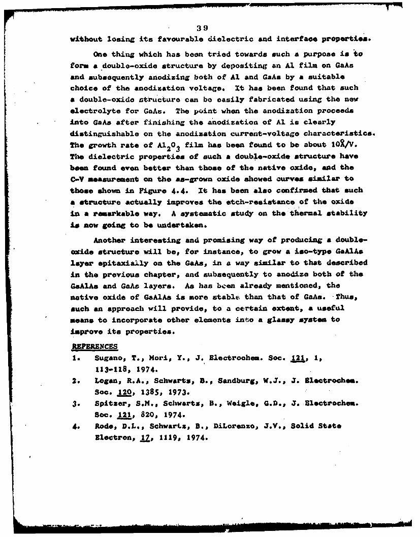
Th',5 zur-c iu Fkruro 4.2 is a t:,ical variation of
anodvatiou currea.t versus U V~ifcr.aI glarsy oxide layerswith well-r'.ofircd intcrc'icc colo,_7, r:!o Cr-wn wit-hin 10-20
32
minutes at room temperature, up to a thickness of about 7000R,
--.,depending onthe voltage applied. The make-up of electrolyte
,-..or the case of Fig.4. 2 is one part of 3% tartaric acid solution
with pH adjusted to.6, mixed wkth four parts of propylene glycol.
The thickness is measured by a Zeiss interference micro-.- scope and a Dektak profile plotter. As shown in Figure. 4-.3
the oxide thickness changes in direct proportion to the voltage
applied across the formed oxide, at a rate of 21W/V for pm. and
n-type samples with (100) orientations. A similar value is
reported in (2). Although the behaviour of current ve.r.us
time changes with bath parameters, this rate remains barely
.........,,:affected. The amount of GaAs consumed during oxidation is
also shown in Figure 4.3. Comparison with the H202 scheme
reveals that more GaAs is consumed in the present case, to
obtain the same oxide thickness. This could be explained in
two alternative ways, i.e. more of GaAs dissolves into.the
electrolyte in the form of native oxide in the present case, or
the present anodization gives denser oxide films. However,
other experimental evidences on the present oxide such as
that the elctrolyte _hardly. etch the as-grown oxide, that the
as-grown oxide is more impervious against metals in the sense
that it can bear the vacuum deposition of high-melting-point
metals, and that it has a higher resistivity, a higher breakdown
electric fldd strength and a higher dielectric constant, seem
to support the latter alternative.
The as-grown oxides sh,;w well-dt*finud and regular
occurrence of inference colours. Surnc of the data is listed
in Table 4.1. The approximate value 'f the refractive index
estimated from this is 1.8.
The maximum thickness which can be grown by anodization is
limited !-y the electrical breakdown in the oxide which accompanies
sharp spikes in the andization current an( results in a pitty
oxide zurface. It should be noted that, even on such a pitty
surface, mnost of the surface apart from the pits is uniform and
has a regular interference colour corrcspondini to the same
refractive index. This makes a largu contrast to the 1202
anodization scheme (2) where oxides Of different refractive
index start to [,ro: towards the maximum voltage (150^180V) of

33
anodization which finally leads to a completely granular
surface.
The maximum thickness of 700OR obtained without any
electrical breakdown (voltage 350 V)is much larger than the
reported value of 3000 in (2). But, it is still purely an
emprical value and could be further increased by optimization
of the process. It has been noted that the continuous
stirring of the electrolyte becomes very important to obtain
thicker films. For a further substantial increase of the film
thickness, there are two conflicting ideas which could be tried.
One is to cool the electrolyte to increase the breakdown voltage
of the oxide as has been successfully done in the case of
anodization of Si (12), and the other is to heat the electrolyte
to make the ionic transport through the oxide more efficient
(13). It requires future work to see which of these approaches
works better in the present electrolyte, but such an effort to
increase the maximum anodizable thickness seems very important in
view of application to the planar technology. Actually, the
film thickness of 7000R seems already to offer a possibility
of the dielectric isolation of microwave GaAs FET's where thin
epi-layers are commonly used.
As has been pointed out in the previous section, one of
the difficulties of the li202 eluctrolyte system is that it lacks
stability against impurities. For this reason, the process
stability of the present system was studied by additionally
introducing quite strong traces of various common acids and
bases into the electrolyte, and excellent stability was always
maintained. For example, the effect of TICI is shown in
Figure 4.2. In order not to change the gross pH, the pH of the
contaminant solution was adjusted beforehand by NH4OH. Up to
several hundred ppms, no change occurs in the anodization
current, and it only starts to become seriously affected from a
level of a thousand ppm, when the result is still a fairly
uniform oxide layer.
The study of the resulting surface with a scanning
electron microscope confirmed that it is smooth and featureless.
The oxide has chemical properties similar to those in literature
34
(2), being soluble in most of the acid and base solutions except
conc. HNO3 , but insoluble to the halogen-alcohol *chant of GaAs.
The dielectric and interface properties were successfully studied
on MOS devices formed by vacuum deposition of Au or Al and will
be described in the next section.
Though anodization of GaAs has been mainly studied so
far, the present electrolyti3 system appears to possess a large
potentiality for applications to other III-V compcund semi-
conductor materials. In fact, the anodization of a GaxAll1 x
As LPE layer (x<0.3) has been the starting point of this work
as already mentioned in the previous chapter, resulting in a
native oxide which is chemically more stable than the native
oxide of GaAs.
4.3 Dielectric and Interface Properties of the Anodic Oxide.
Experimental MOS capacitors to study dielectric and inter-
face properties of the an(cdic oxide were mainly fabricated on
surfaces cf Zn- doped p- type GaAs bulk materials (Mining
Chemical Product Ltd.) with a carrier concentration of NA =
1.4 x 1017 cm- 3 and (100) orientation. Ohmic back contacts were
provided by vacuum deposition of In and Ag films with a
subsequent brief annealing at 6000 C in H2. Surfaces to be
anodized were polished chemomechanically in an aqueous solution
of sodium hypochlorite. Care was taken to minimize possiblc
contamination by sodium ions and by other sources. After a
thorough rinse of the polished surface, nearly 104 A of GaAs
was etched away from the surface by a repeated process of
anodic oxidation followed by dissolution of the oxide in an
HCI solution. Then, the oxides to be studied were formed in a
fresh electrolyte. The composition of the electrolyte was ')ne
part of 3% aqueous solution of tartaric acid mixed with two to
four parts of propylone glycol. A Pt or Al cathode was used
anG oxides of 1800-20005 thick were formed. To form field
plates Au or Al dots 400-425 pm diameter were deposited in
vacuum through a metal mask. Apart from careful bridge
(Boonton, General Radio) and electrometer (Keithly) measurements,
of capacitance and leakage current respectively, dynamic
measurements and rapid assessments of interface properties arc

35
.performed with 'an automatic C-V plotter which wqp s pecifically
_.devel)46d for tbl'purpose and whose details wil..be given in
'the next Chapter and Appendix. This C-V plotti~ng system can
-m~a'sure the C-V characteristic"f'or a frequency range from 100Hz* to,2-.5,Wz with sweep speed ranges of lOmV/s. to.5V/s for the
field plate voltage. For all measurements the !40S capacitors
are enclosed in an electrically shielded light tigh9t box.o
As-grown oxides were found tQ have a breakdown fiei .
strength of 4-5 x 10⁶ V/cm, a prebreakdown leakage-ourrent"
density of 10-11 to ,0-9 A/cm2, and a specific resistivity
ranging fr om 1014 to 1016 Qcra. These values are' l63,-..105ti.mes 'larger than the 'previous results on native. ox*de of.GaAs (2) and a-re approaching the quality of therrmally grown
8i0 (1.). The relative permitivity measured at "HZ is 7-8
which is-considerably larger than the value of 5.4 ro-ported in
(2).
A typical C-V plot of one of our MCS-,capaoitors befor-o
afnealihg is shown in Figure 4.'!. It has been shown by
-t:p~rbvious'authors that the properties, of the interface beitw--n
GaiAs and various deposited oxides (Si .N~(5(~ i 2 -l)
A1203, Si02 - Al0 (1(19) are much more complicated than
those of 81'- SiO2 interfaces. The main problems-associated
witn C-V characteristics of such GaA§_NOS capacitors-are (i)
fibld-&n1.hduced hysteresis which is ob~servable at room..
terfperature, (ii) large frequjency, 4isp( rsion of the accumulation
'capacitance-at-low frequencies, and ,.,iii.) a high densty-of fast
interface states (mostly in the rangeof, .101.2 -11c~w
The results in Figure 4.4 show that such. a complicated
.behaviour is also present with the anodic rjatlvo oxide,-vhert.
*a fairly large hysteresis is shown which gives an effective
flat-band voltage shift AVF of about l5V ,f~r the..applied
,field of 1.1 x 10⁶ V/cm. This hysterqsis has an oppositedirection from that of the positive-Ijon instabil~ity in
Si-SiO2, and can be explained by a trt.p filling mechanism
where traps, distributed in the oxide, are filled -and emptied,
by-electrons tunnelling from and to the semiconductor.-,
The large frequency dependence of the cap-acitarice, evreft
in the accumulation region seemns to indicate that an inoompletely

36
oxidized and therefore fairly highly conducting layer in present
near the interface which effectively reduces the oxide thickness
at low frequencies (the classical Maxwell-Wagner effect (20)).
The presence of such a layer has been actually confirmed by Itob
et al (18) in the case of A1203 - GaAs and S102 - A1203 - GaAs
interfaces using ellipsometric means and has been termed a
*meta Aorphic layer*. Sugano et al (1) have also shown by
plasma oxidation of GaAs (a gaseous analogy of anodization)'
that a native oxide with a fairly low resistivity (108-101O )
is formed under a very rppid growth condition. A simple
analysis of the experimental data suggests that the "meta
morphic" layer should have a thickness of 150-200 with aresistivity of around 108 Qcm in the present case.
The positive voltage branch of the C-V curve in Figure 4.4
shows an effect typical of deep depletion for a sweep speed of
the field plate voltage of 2.6 V/sp indicating a slow
generation rate of minority carriers in GaAs. A similar effect
has been reported in the case of GaAsF (21). This dynanic
behaviour disappearsp of coursej as the sweep speed is reduced
Also within the measured frequency range down to IOOHz, only a
so-called "high frequency, characteristic has been observed
which is again consistent with the slow generation rate of
minority carriers.
The effect of a short-time, relatively low-temperature
annealing of such an oxide is shown in Figure 4.5. Hydrogen
gas was used because low temperature annealing (S00C) in N2
is known to be very effective in Si MOS technology to reducefast interface states owing to a certain complexing mechanism
of structural defects which are the origin of such states (22).
Remarkable improvements are clearly seen by comparing Figure 4.4
with 4.5. The hysteresis has been reduced by a factor of 15 in
terms of V., for the same field strength, which means roughlya reduction of the slow trap density by the same factor. The
frequency dispersion of the capacitance in also almost reduced
to zero, which indicates an extinction of the "meta morphic
layer". Estimates of fast interface-state densities N have
been conveniently made from the difference between the high-
frequency capacitance C., and low-frequency capacitance CLF
through the following equation (23).

37
. . - , [ 5 ..? s a v a i l a b l e C O P Y . _
N C CLF/Ci -F/Ci
1 - QLF/Ci I .CHF/Ci
where Ci is the insulator capacitance. The result for the-
annealed oxide shown in Fig. 4(b) is that N., is about
6xlQ'1cm-2 eV-1 near mid-gap.
The improvement which has been achieved'by annealing'is
ip .sharp contrast to previous reports on deposited oxides where
annealing has been found ineffective, aid seems-tosuggest the
importance of having a "native" oxide in -order to-obtain a
natural and less defective interface structure. -v,:.-
Extensive annealing experiments, using variois'arI ling
temetatures and times, have shown that the optimum annealing
temperature for such a native oxide is around 3000C. A naling
at 4000 C .for 1.5 hr. in H2 , reduces the oxide thidkness : ':about
30 .ndlqompletely changes the oxide color, possibly by the
:asublimitio n of As oxide (24). Although the oxide still"geems
very uniform the breakdown voltage is reduced to 1.5-kx1q50V/cm
and the direction of the C-V hysteresis is reversedV'., 1"
On the other hand, no appreciable change in oxide thick-
ness color or dielectric properties has been observed'after
times as long as 6 hours of annealing at 3000C in H2 gIas. The
effect of annealing has been found to be very reproducible.
The bbst result so far obtained by a longer annealing time is
summarized -in Table 4.2.
The result in Table 4.2 certainly indicates the large
pot-entiality of the anodic oxide towards various OS applications-,.... on GaAs. ThereforL, further systematic study is urgently
needed in the future to establish the most suitable processing
of such a native o;ide, optimizing th(e growth c3nditions and
post growth annealing conditions (gas species and temperature).
Another important feature is the stability study of the'0xide
where electrical, chemical and thermal stability should be
established and optimized, including the bias-temperature
treatments which have not been done so far. On the basis of

38
the results reported in Chapter 2 and also of work by Cooper
et al (16), both of which indicate that the widely accepted
model of a MOS capacitor (25) bccomes inadequate in the case
of GaAs, a more appropriate model of GaAs MOS capacitors should
also be developed, usin. the results of more detailed C-V andconductance measurements,
A certain work on the actual MOS device fabrication
using the present oxide han already been started and will
be briefly reported in Chapter 7.
4.4. A New Double-Oxide Structure using Anodization Techniaue
As compared with Si0 2 obtained by the thermal oxidation,
the present anodic native oxide of GaAs has a poorer chemical
and thermal stability. It dissolves into most of the acid
and base solutions. The as-grown oxide is etched even by pure
water although it occurs extremely slowly (below lO' 21/sec).Such a property could be uaoful in cortein applications such
as the controlled ctchling of GaAs (4) but, in generals, it
imposes a cc-.tain limitaticn on the processing application.
Fortunately, it dozz not dissolve into usual organic solvents
and halogon-alcohol otehants of GaAs both of which are very
useful properties for ruch -rnlicntions. It ha- been also
shown that tVhefot' trctnent of the preoent oxide above 3500C
resulto in a change in the oxide itself, leading to deterioration
in the dieloctric and intorfnco propertiei. Although 3500C is
much higher than tho ,tztal davico operation temperatures&, such
a property again imposes a sever4. limitation on device processing
such as diffusion and ohmic-contact alloying, and could also havean effect on the long-term stability 4f devices.
The present native oxide is thought to be a glassy
mixture of gallium oxide and a.-senic oxide as has been demon-
strated by Feldman et a! for a cimilar oxide (24). The
chemical and thermnl instability of the oxide is most probably
coming from the arsenic oxidn part which is apparently the
glassy network former of tho pr.naent oxide, Judging from the
known propertio3 of galliun oxid.cs and arponic oxides.The essential question would be now how one can possibly
enhance the chemical and thernal stab3.1ity of such an oxide
39
without losing its favourable dielectric and interface properties.
One thing which has boon tried towards such a purpose is to
form a doublo-oxide structure by depositing an Al film on GaAsand subsequently anodizing both of Al and GaAs by a suitable
choice of the anodization voltage. It has been found that such
a double-oxido structure can be easily fabricated using the newelectrolyte for GaAs* The point when the anodization proceeds
into GaAs after finishing the anodization of Al is clearly
distinguishable on the anodization current-voltage characteristics.
The growth rate of Al203 film has been found to be about 101/V.
Tie dielectric properties of such a double-oxide structure have
been found even better than those of the native oxide# and the
C-V measurement on the as-grown oxide showed curves similar to
those shown in Figure 4.4. It has been also confirmed that such
a structure actually improves the etch-resistance of the oxide
in a remmrkable way. A systematic study on the thermal stability
is now going to be undertaken.
Another interesting and promising way of producing a double-
oxide structure will be, for instance, to grow a iso-type GaAIAs
layer epitaxially on the GaAs, in a way similar to that described
in the previous chapter, and subsequently to anodize both of the
GaAlAs and GaAs layers. As has been already mentioned, the
native oxide of GaAlAs is more stable than that of GaAs. -Thus,
such an approach will provide, to a certain extent, a useful
means to incorporate other elements into a glassy system to
improve its properties.
RBBERENCOS
1. Suganop T.p Mori, Y., J. Blectrochem. Soc. 121# 1,
113-118, 1974.
2. Logan, R.A., Schwartx, D.p Sandburg, W.J., J. Slectrochem.
Soc. 120, 1385, 1973.
3. Spitzer, S.M.# Schwartz, B., Weiglep G.D., J. Blectrochem.
Soc. 121, 820, 1974.
4. Rode# D.L., Schwartz, B., DiLorenzop J.V., Solid State
Electron, jZp 1119, 1974.

* - 40
REFERENCES
5. Duffek, E.F., Benjamini, E.A.,.Mylroie, C., El'ectrochem.
Tech. 3, 75, 1965.
6. Nedberg, L.G., .Final Year Honours Thesis 343/1969, Dept.
of Electrical & Electronic Engrg., Univ. of Newcastle
upon Tyne, .1969.
7. Haden, C.R. et'al IEEE"Journ. .of Solid-St.. Cir., SC-9,
118,- 1974.
8.v Schwartz, -B.,'J. Electrochem. Soc. 118, 657,-1971.
9. Burger, R.M., Donovan, R.P., Fundamentals ofSico
integrated Device Technology Vol. 1 (Prentice-Hall,Englewood Cliffs N.J. 1967-see p.60).
10. Stoneham, E.B., J. Electrochem',;Soc. 121, 1382, 1974.
11. Muller, H., Gyulai J.'; Maybr,*J'.W.,yEise n, F.H. , Welch~ Be,presenteci at '74 Ion Implatation Coaf. Tokoyq, Jpa,papjr~.-2, p16, 1974.
12. 3esearch Triagle Institute, Selected Experiments in-
Silicon IntOgrated Device Technology, Technical D~ocumen-
tary Report No. AF-TDR-64-29, March, 1964.
13. Schwartz, B., private communication.
14. Burger, R.M., Donovan, H.P., Fundamentals of Silicon.Integrated Device Technology Vol. 1 (Prentice-Hall
Englewood~liffs N.J., 1967 p1O8 ).
15. Foster, J.E., Swartz, J.M., J. Electrochem. Soc. 2 117,
11, 1410-.1417, 1970.
16. Cooper, J.A-, Ward, E.R., Schwartz., R.J., Solid-wStateElectronics, 15:, 11219-1227, 1972.,
17. Kern, W., White, J.P.., RCA Review, 31, 771-785, 1970.
18. Ito, T., Sakai, Y., Trans.* I.E.E. J., 93-A,11, 1973.
19. Ito, T., Sakai, Y., Solid State Electronics, 17,751-7Z59,
1974.
20. Von Hiippell, A.R., Dielectrics and Wares, (Wiley, New
York, 1954, 412-424.

REFEBECES
21. Forbes, L. et al ,Solid StatelElectronics, 17, 25-29,1974.
22. (see for eximple) Deal, B.E., J. Electrochem. Soc. 121,6, 198C-2O5it, 1974.
23. Castagne, R., C.R. Soc. Paris t267 Serie B 866, 1968.
24. Felddman, L.C., Poate, J.M., Ermanis., F., dchwvatz, A.,Proc. Int. ConX. on Ion Beam S~rface Layer Analysis.Yorktown Heights, N.Y., June 1973.
25. Nicollian, Eli.r ,Goetzberger, A., Bel11 Syst. Tech. J.46
1.05, 1967.
Reproduced from
FIGURE CAPTIONS
4.1 Experimental set-up for anodic *oxidation of GaAs.
.4.2 Aiodization current versus time,'including the effect ofHC1 contamination. Electrolyte: one part of 3% tartaric
acid solution (p11=6-) mixed with four parts of propylene
glycol.
of3 Thckes artaricai d solution . El=iedtrwit: ton part
4.3 T3ces tatrc aislivoltge El=) ie trolt:on part
of propylene glycol.
4.4 C-v curves of a MO0B capacitor for the as-grown oxide.
4.5 C-v curves for a MOS capacitor after annealing at
3000C.

Ea Rs
Pt CATHODE
pYREX
- - CAPILLARY TUBE
-: ------
- GuMA SAMPLE
ELECTROLYTE
STIRRER
Fig. 4.1
1Experimental set-uP for anodic oxidation of GaAs
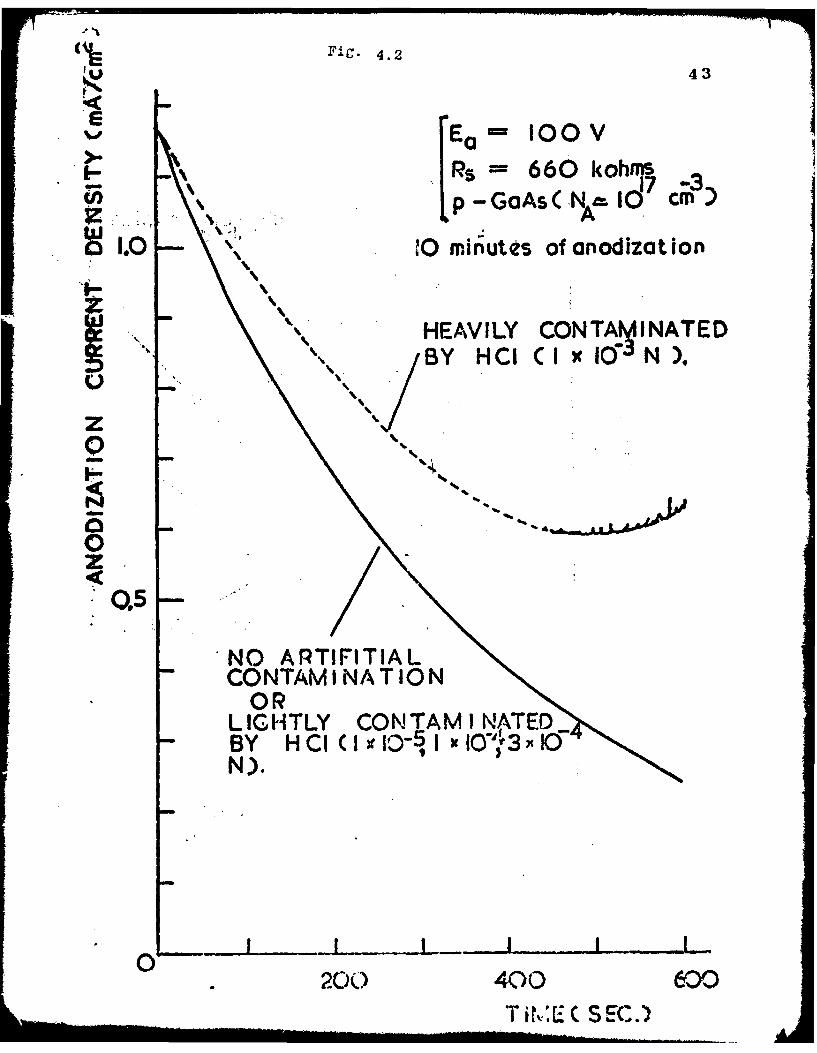
( Fig. 4.2
43
Ps = 660 koh ..p-GaAs (NA IT o,)
1. 10 minutes of anodization
HEAVILY CONTAMINATEDBY HCI C I xIVO N)X
0z'mu..
05z
NO APTIFITIALCONTAMINATION
ORLIGHTLY CONlAMI NATEDBY H CI(I I - I IO" 34 IOtN).
I!I I
0 LJ200 400 600
,T • ti,. E S SEC,.

Fig. 4.3
Thickness versus applied voltage. Electrolyte:
one part of 3% tartaric acid solution (pH=6)mixed with two parts of propylene glycol
GaAs < 100>
o OXIDE on p-typeC NA 1017 cr - ) ch momechanicaly
3 - OXIDE on n-type( N ~i ns cr6f3)
0< NTk1
O A GaAs consumed (p-type)00
OXIDE THICKNESSClinear up to 350 V,
2 71OO Az
UA
I- /0
I GaAs CONSUMED
0 50 100 150VOLTAGE C V)
10 A
InS .>,
-0 X
014.1e, >
,4 0 - -
0 ;.
I/VI0
LA.
LA.
i n0
InI
Fig. 4.4
C-V curves of a MOS capacitor for the as-grown oxide

Fig. 4.5 4
C-V curves for a Mos capacitor after
annealing at 3000C
rr
zz00 >
0

47
TABLE 4.1
INTERFERENCE COLOURS OF ANODIC NATIVE OXIDE OF GaAs
condition : observed perpendicularlyunder fluorescent light
4.ickness I colour
500 brown
800 dark violet
1000 royal blue
1300 light blue
.600 light green
1700 yellow
1800 gold
2200 red purple
2400 dark blue
2700 green

48
TABLE 4.2
INTERFACE PROPERTIES IMPROVED BY ANNEALING
IN H2 GaS
Annealing conditions 3000 C for 6 hours
1. hysteresis in below 400 mV for applied
terms ofVVFB field of 1 x 10⁶ V/cm
2. frequency dispersion change over the frequency
of accumulation range of 100Hz - 1MHz is
layer capacitance~ below 1%
3. fast interface 1-2 x 1.011cnV2eV-1 near
state density the mid gap

49
CHAPTER 5
ASSESSMENT OF INTERFACE F'ROPERTIES
(K.E. FORWARD)
5.1 IMOtURODUCTION
The best method of assessing interface properties is to
use C-V plots at high and low frequencies. Details of the
methods of determining fast interface states Nss, fixed change
Qss and trap densities NT from these curves are given in
Deal (1), Grove (2), Sze (3), Castegne (4), Fahrner (5), Kern
and White (6). The basic requirements are plots of C--9
against bias voltage at various small signal frequencies.
The plotting of these curves point by point with thi aid of a
bridge has the obvious disadvantages of operator frustration
and the consumption of valuable time which could be better spent
on other tasks less easily automated. We therefore devoted
considerable time to the development of an automatic C-V plotter.
5.2 C-V Plotting System
The details of the C-V plotting system developed is
described in Appendix 1, but the specification is given again
here as it is relevant to the discussion below. The system
has a sensitivity of 7 mV/pF for 25 mV pp signal applied to the
sample. The frequency range is from 100 Hz to 2.5 MHz and the
bias voltage range is ±30 volts. The ramp can be applied at
rates from lmV/S to 5v/S, and the drift rate in the hold
position is 0.01 mV/S. The instrument covers the range from
0 to 100 pF but could be modified to extend this range to
higher values if necessary.
5.3 Application
The instrument is usually used to plot small signal
capacitance against bias voltage but it can also be used for
the slow ramp technique of Castegne (4) to obtain low frequency
C-V curves. By applying a step instead of a ramp and then
observing C as a function of t~me, the retention time of MOS
capacitors can be measured, Sah and Fu (7), (8). This is a
useful technique for assessing the usefulness of MIS systems
601-

50
for CCD applications.
5.4 Discussina of C-V Plotter
As mentioned previously, a complete description of the
C-V plotter is given in Appendix 1. It has proved a very
useful tool in this work and enables extremely rapid assessment
of the effects of various processes, such as annealing. Care
is required in its use and in the interpretation of results as
factors such as ramp speed and signal amplitude can cause
spurious results. The input signal amplitude also requires
careful adjustment and must not be allowed to drift as the
output is proportional to the square of this voltage and is
hence sensitive to very small changes. The system must also
be recalibrated before each measurement as the end results such
as Nss and Qssare obtained from differences in two or more
readings. As these might be quite small differences in the
lirge numbers small errors due to drift in the instrument can
cause quite large errors in the results. The sensitivity and
zero level also change slightly with frequency so it is
essential to recalibrate before each reading and especially if
the frequency has been changeJ. Due to the very small signals
used and the high gain of the sigaal amplifier shielding from
mains hum and stray electromagnetic signals is essential if
errors from this source are to be avoided.
REFERENCES
1. Deal, B.E., J. Electrochem. Soc.. 121, 6, 198C-205C, 1974.
2. Grove, A.S., Physics and Technology of Semiconductor
Devices, John Wiley & Sons, U.S.A., 1967.
3. Sze, S.M., Physics of Semiconductor Devices, Wiley,
N.Y., 1969.
4. Castegne, R., C.R.Sc. Paris, 267, Serie B, 866, 1968.
5. Fahrner,W., J. Electrochem. Soc. 120, 1973.
6. Kern, W., White, J., R.C.A. Review, 31, 771, 1970.
7. Sah, C.T., Fu, H.S., Phys. Stat. Soc. (a) 11,297, 1972.
8. Sah, C.T., Fu, H.S., ribid 14. 59, .972.
9. FDrbes, L. et al Solid-State Electronics, 17,25-29, 1974.

5'
CHAPTER 6
ADDITIONAL PASSIVATION SCHEMES INVESTIGATED
6.1 INTRODUCTION
The four main techniques available for the depositionof insulators are:-
(i) Vacuum deposition (sputtering or evaporation)
(ii) Liquid coating followed by solvent evaporation
or chemical reaction which converts the liquid
to a solid
(iii) pyrolitic decomposition of suitable gases
(iv) Deposition of an element followed by anodic oxidation.
It would also be possible to carry out the oxidation
in (iv) pyrolitically but the sublimation of As from GaAs at
relatively low temperatures precludes this method. Method (iii)
has also been excluded by us on the same grounds but has been
attempted by others(l) with limited success.
In this chapter, additional passivation schemes
investigated are briefly described. They include four different
ways of insulator deposition, i.e. use of spin-on Si02 , A£203deposition by anodization, electron-gun evaporation of AZ20 3 and
a precipitation of As203 layer from a liquid solution. Theyalso include a different way of native oxidation using a Na0CZ
solution and also a somewhat different approach of using proton
bombardment. Some of them have turned out less promising and
some seem still worthwhile pursuing further.
6.2 Spin-on SiO2 films (K.E. Forward)
An attempt was made to use Silicafilm, a product of the
Emulsitone Company, which employs method (ii) above to coat GaAs
with Si02 using the following procedure. The GaAs in waferform was polished to a mirror finish using a chemomechanical
polishing technique. Then the surface of the GaAs was etched in
a polishing etch of either Br-methanol or NH4OH : H202 : H20

52
to remove the possibility of Na ion contamination. The surface
of the GaAs was then oxidized by exposing it to 02 for one hour
at 5000 C. This latter step was necessary to ensure the
adherence of the Si02 film. The silicafilm suspension was then
applied to the GaAs and reduced to a 2000R thick film by spinning
at 6000rpm. The resulting Si02 film was then baked at 900 C
for one hour and finally sintered at 2500 C for two hours. Al
field plates, about 400um diameter were then evaporated through
a metal mask to form field plates. Capacitance and conductance
were then determined with bias voltage as a parameter, using a
Boonton Bridge. Then using the method of the conductance
technique by Nicollian and Goetzberger (3) the density of fast
interface states Nss was determined. The results were not
encouraging for many reasons.
The disadvantages of spin on oxide were that it di Jt
coat evenly, due to edge build up which is not very serious and
to channeling of the solution from the centre during spinning
which is much more serious as it resulted in radial ridges in
the final film. The film of Si0 2 did not adhere to the etched
GaAs without pre-oxidation as described above and this means that
the undesirable double layer hysteresis effects reported by
various workers (4) (5) are unavoidable. The Si02 films also
craze if heated to temperatures above 5000 C, due to differential
expansion at the GaAs and Si0 2 interface, unless the SiO2 films
are less than 2000I thick. The density of interfaces states,
Nss, was also rather high at 2 - 4 x 1012 cm-2 eV- 1 . In some
cases spin on Si0 2 films may be of some use and N., may be
reduced by annealing but due to the fact that we have developed
more successful techniques the method was abandoned after these
initial experiments.
6.3 Anodization of Al (K.E. Forward)
The vacuum deposition of Al is extremely simple and can
be carried out using either an electron beam gun or a resistive
heater such as a 3 or 5 core tungsten wire hairpin coil or
basket. This is in strong contrast to A1203 which is a
refractory material which can only be successfully evapoured
in an e-gun. The ease of Al deposition therefore makes the
- " .. . .... 'lt ~ l | t a . H=. ........m-

53
technique of depositing Al and subsequently anodizing it to
produce an A12 03 film most attractive. There are many reports
in the literature on the anodization of Al and provided a
suitable electrolyte is used extremely dense film with excellent
electrical properties can be grown (6) (7) (8), as also
described in Chapter 4.
Before we succeeded with our new anodization of Chapter 4,
there were several negative results. Using the electrolyte
specified by Francis (6) or that of Davies (7) we were able to
anodize Al on glass. However, when Al on GaAs was used as the
anode, the only result achieved was the etching of the GaAs and
this removed the A1203 film. H202 30% aqueous solution as
reported by Logan et al (9) was then tried but due to the effect
of impurities this also failed to produce the desired results.
The failure of H202 as an electrolyte for this purpose is not
surprising as Logan et al reports that as little as 2 p.p.m. of
strong acid is sufficient impurity to convert the anodization
into etching . We could not even obtain H202 of that purity.
From the experiments it was concluded that in order to be
able to anodize Al on GaAs an electrolyte would have to be found
which could be suitable for GaAs as well as Al. H2 02 , which
was then the only known electrolyte in which GaAs could be
anodized, requires such high purities that it is not a very
practical solution. Only the anodization of GaAs in a glycol el-
ectrolyte, as described in Chapter 4, produced positive results,
producing a highly corrosion-resistant double-oxide structure.
6.4 e-gun evaporation of Al203 (K.E. Forward)
Although Dr. Hill at the Newcastle Polytechnic gave us
much of his valuable time we were not able to obtain useful
results with his equipment. Firstly alumina proved to be an
unsatisfactory source due to outgassing. It was therefore
decided to use single crystal A1203 in the form of artificial
ruby. The problem was attempted with the help of another local
laboratory and A1203 was successfully deposited. However, the
eiectrical assessnount has not yet been completed and the results
are going to be reported at a later date.

54
6.5 Passivation with As0 3 (B. Weiss)
It has been shown by Kyser and Millea (10) that the
chemical etching of GaAs in concentrated nitric acid solutions
produces a layer of arsnic oxide on the surface of the sample.
Several samples of (II) orientated GaAs were etched at
room temperature in a nitric acid solution, containing one part
cone. HINO3 with one part distilled H2 0 by volume, for five
minutes. The resulting oxide layer was examined in the S.E.M.
Due to the insulating nature of the sample surface it was coated
with a 3002 thick layer of gold to prevent it charging up.
S.E.M. micrographs of the surface of the sample are shown in
Figure 6.1 and they show that these layers are quite flat
although considerable work is required to produce more uniform
layers suitable for MOS devices and surface passivation.
6.6 Native Oxidation of GaAs using an aqueous solutionof NaOC1. (R. Hasegawa)
During some studies done in this laboratory by Hartnagel
and Weiss (2) of etch polising methods., it was discovered that
sodium hypochlorite is a di-:cation-revealing etch for (1ll)
GaAs and that it produces fter some initial etching a stable
and reasonably etch resistant thin native oxide layer. It
certainly means that this etchant removes only GaAs during the
initial period. Sodium hypochlorite is therefore primarily
employed for etch polishing when the oxide formed is continuously
removed by mechanical action. It was obvious that this
solution should be further explored in connection with its
oxidizing property.
As a result of further study, it has been confirmed that
a stable and highly etch-resistant thin native oxide layer can be
formed by placing polished GaAs chips into a dilute aqueous
solution of NaOCl with a volume mixing ratio of typically from
20:1 to 50:1. The resulting layer is opaque with a whitish
colour. It shows, under a microscope, a crystallite structure
rather than a vitreous state. The film thickness obtainable
by this method is restricted to several hundred angstroms,
possibly because the oxidizing agent cannot diffuse through the
grown native oxide layer. More concentrated solutions have been
~55
tried to increase thicknes 9 but it resulted in very dull
surfaces.
The highly etch-resistant nature of such a film is
oertainly interesting as compared with the chemical properties
of the anodic native oxide described in Chapter 4 where the oxide
is readily soluble to most of acid and base solutions. It seemsto suggest that during the oxidation by NaOCI As atomw of GaAsdissolve into the solution in a certain form of oxide, whereas
Ga atos remain on the surface, being oxidized and form a verystable crystal structure such as P-Ga20 3 or similar structure
including Na or Cl. A glassy structure cannot be formed because
basically the Ga atom is not a glass network former while the
existence of glassy As2 03 is well known. As203 is also known
to dissolve into water depending strongly on pH (II). However.
the above explanation is only a speculation and needs, of course,a detailed chemical analysis.
In conclusion, this approach of native oxidation has now
turned out to be less attractive primarily because of the limited
thickness available and the crystallite structure, where grain
boundaries can have detrimental effects for the practical
passivation applications, and also in view of the highly probablecontamination by sodium ions which might lead to serious ionic
ipstabilities encountered in Si ?IOS technology.
6.7 Passivation with semi-insulating GaAs and GaAlAs layersproduced by proton bo(Hbardent (. Hasegawa)
In connection with the epitaxial approach for the
passivation described in Chapter 3, an alternative method toform a semi-insulating semiconductor material is to use protonbombardment. Use of such a technique for GaAs junction device
isolation has been described by Foyt et al (12). GaAlAs can
also be converted into semi-insulating shown by Favennec
et &l. (13).
The actual mechanism which is responsible for such asconversion has not been established but seems to be closely related
to the disorder in the crystal produced by the bombardment.
In order to see whether such a technique is useful forpassivation purposes, proton bombarded n-GaAs and n-GaA2As

56
samples were produced with the aid of the Physics Department
at the University of Salford, U.Kf The proton energy and dose
used in the experiment is 40Ke V and 1013 1/cm3 , respectively.
..... Accordig to the literatures (12) (13), the thickness of the
resultant semi-insulating layer should be about 40002. To
investigate the electrical properties, an-Al field plate was
provided by the standard technique. Careful. electrical
measurements at small bias voltages indicated the .presence.of
a highly resistive layer. However, the breakdown voltagebof
such "MiS" devices have been found unfortunately veryswmal,
typically wound 1V, and therefore no meaningful C-V m~auroments
have been done so far. Within the measured range, no,.
.appreciable change in the capacitance was observed.,......
. The present results seem to indicate that.the::tden.que
-- proton bombardment is not suitable to "MiS" applicatitog, or
,insulation of metalization patterns as is employed in Si-J anar
technology. However, for the purpose of.producing".aaN7-
"electronically" passivated surface with reduced interface states
and traps, the question must be more carefully investigat.ed
because such a technique could still provide a better .nterface
as compared with the exposed air-GaAs interface which would have
an interface state density larger than 1013 1/cm3 . If.tbe usual
dose of 1012_1013 1/cm2 has actually a one-to-one correspondence
to the electronically active disorder- in the semiconductor and
the carriers in the active semiconductor can make frequent
'charge transfers across all these defects, there is no hope, but;
these assumptions seem unlikely to hold. In fact, there is a
certain experimental evidencc that the performance of GaAs
devices, in particular, Impatt devices, can actually be improved
by proton bombardment along the device periphery. Further study
is therefore required to clarify the interface properties of proton
bombarded GaAs layers.
*We should like to express our gratitude to Professor G. Carterand Dr. W. Grant of the University of Salford where our slideswere proton bombarded.
*1"'

REFERENCES b 7
1. Ito, T., Sakai, Y., Solid State Electronics, 17,751-759,
1974.
2. Hartnagel, H.L., Weiss, B.L., J. Mat. Sci., 8L 1061, 1973.
3. Nicollian, E., Goetzberger, A., Bell. Syst. Tech. J. Vol.
46, 1055, 1967.
4. Foster, J., Swartz, J., J. Electrochem. Soc. 117,1410,
1970.
5. Cooper, J.A., Ward, E.R., Schwartz, R.J., Solid-State
Electronics, 15, 1219-1227, 1972.
6. Francis, H.A., J. Electrochem. Soc., 112, 12, 1234-1237,
1965.
7. Davies, J.A., et al J. Electrochem. Soc., 112, 7, 675-680,
1965.
8. Haden, C.R., et al I.E.E.E. Trans. S-C 9, 3, 1974.
9. Logan, R.A., et al J. Electrochem. Soc., 120, 10, 1385-
1390, 1973.
10. Kyser, D.F., Millea, M.F., J. Electrochem. Soc.
11. Schwartz, B., J. Electrochem. Soc., 118, 657, 1971.
12. Foyt, A.G., Lindley, C.M., Wolfe, C.M., Donnelly, J.P.,
Solid-State Electronics, 12, 209-214, 1969.
13. Favennec, P.N., Diguet, D., Appl. Phys. Lett., 23,
546, 1973.
FIGURE CAPTIONS
6.1 SEM micrograph of arsenic oxiae layer.

58
2I
l --
SReproduced from6est available copy.
Fig. 6.1
S.E.M. micrograph of arsenic oxide layer

59-
CHAPTER 7
FABRICATION o,. DICES
(..E. FORWAPD)
The fabrication of two devices is currently in hand an)40S trinsistor and CCO. Both of these will be made in GaAs
using :the Gas/(GaA) Oxide described in Chapter 4 to obtain"Planar structures. The work so far carried out on tbe. FBT
is described first as this is more advanced than the CCD..
7•1 .aAs-'IOSFET
A GaAs-OSFET has been fabricated on an epitaxial layer
9p thisk oa..an n-substrate, using native oxide insulation.
The fabrication details are given here to provide a convenientreference for workers at these laboratories who will continue
ths.. work.
7.1.. .Fabrication
The mask set is shown in FiGure 7.1. The process steps
are given in Figure 7.2 but a few extra notes are needed to
avoid repeating mistakes of the past. In steps 3 and 4, the
anodization rate of 21X/Volt is used to determine oxide thickness
where the voltage is that measured between the sample and the
cathode at a current of 20A. The films have in some cases
been grown at constant current density of about So mA cm"2
but the current has always been reduced to 20A to determinethi.:itormtion voltage. When photo-lithography is used in anyphoteorlthographic step it must be remembered that the Shipleydev6loper-,is a strong base which rapidly dissolves the (GaAs)oxide. - This is useful as the photo-resist' can be developedand-the Windows opened simultaneously.
Another point that must be made is *hat when using
the Shipley 1350 the developer needs to be mixed I : 4,resist z water, in order to be strong enough to develop theVery narrow gaps used in these masks. The standard I s 10
mixture'is too slow to ensure complete development. For

60
both Shipley and Kodak resists 20 sec. exposure times have been
used. An unfortunate feature of the native oxide is that itrea~cts with Sa above .23240c -to procduce~tan almost insolublepowder which is extremely difficult to remove from the GaAs.
Alloying of the Sn:Ag junctions must .not be carried out using
GaAs (Oxide) as a mask for this reason. Before any further
progress can be made on this project both negative and positive
mask sets are required to ensure complete freedom og cho~,ce
of esitAbec~Ause in somo cases, Kodak Micro-n g-rss mustbet used as it has the advantageof developing in an papanicliquid which doos not attack GaAs (Oxide.). Yet in other casesShipley resist must be used as it is readily soluble in
acetone while Kodak resist is softened by boiling triloro-
*eti~n.and removed -with -a cotton bud. In step 1 the drainand.:source metalizations are -delineated -using the Shiple$,
-I .1vex"sist float-off tcchniqu3. The nativas:oxides have been{..,._...Auccssfully growvn using 5O mk/cm2 Anodization. current and
measuring the formation voltage at a current of 0.5mA/cW_*
The oxicIo will thien bo 21R thich per volt.Reruedrm
7.12 Dscusienaf~QSf-'i~aio~best available copy.
The main problems encounte-7ed are concerned .with the
photolithography.. The most obvious problem from the aboave isC.the.;harsh. caustic developer used with Shipley resist.- ,Z'b. would:-- be. much :better to~ workF witsi Kodak Micro-Neg. or Emulsil'one
-.resist.. The Y~odakc rcair't utses organic solvents for its:developer 2nd for its rinse, while the Emulsitone resizb
develops in water. These resists are both negative andt-so our
mask set is unseuitablo.. It would be well worthwhile making a-'new set suitable fo' .negative resicts, as both Kodak Micro-Neg.
and Eaulsitono 4re itociced by. this laboratory. The IOIL linewidth for. the dijode windown is too narrow and needs to be
opened up to t; leant 2011 and pribably to 309&. Masks which
have .10p lines only on them also require aligning mrzks at least
30OA wide, as it is irn'-,ozrible to observo the surface of the chip
throu .,a 10g. Wide olot., Those prol3erns o.line widths and
a;lignment marks could be overcc-p -at the time the negative mask.are produced. Thla is not to soy that the present set, of
mask& is impossible to use but they are more difficult to use
than they need to be. Fabrication of this MOSFET has taughtus a lot about device r-ocertaing using native oxide as an

61
insulator and mask and this experience will be invaluable
when the CCD's are fabricated.
7.2 Charge Coupled Device (CCD)
The CCD is essentially an interdigitaled electrode
structure with a very fine inter-electrode sptcing. (An
excellent review of CCD technology and application is
contained in the International Conference Proceeding,
Technology and Applications of CCD's, Edinburgh 1974). In
order to achieve this very fine spacing we intend to deposit
one set of electrodes using Au which will then be covered
by several hundred 2 of Al, which will then be anodized.
The second set of electrodes will then be deposited over-
lapping the first. The spacing of the electrodes at the
surface of the insulator will be determined by the
thickness of the oxide layer which will be 500 to 1000
thick, giving a very fine spacing indeed. In addition
to the narrow spacing a stepped gate structure as required
for 2-phase operation is also obtained. The set of
processing steps is similar to that shown in Figure 7.2 and
an explanation of each step is already given. The mask
set-for an 8 cell CCD and a set for a 64 cell CCD have been
cut and are shown in Figure 7.3 and Figure 7.4. This
work will be continued by Mr. Bayraktaroglu.
FIGURE CAPTIONS
7.1 Mask set for A GaAs MOSFET.
7.2 Process Steps of MOSFET fabrication.
7.3 Mask set for a 8 cell GaAs CCD.
7.4 Mask set for a 64 cell GaAs CCD.

62
Fig. 7.1
MASK SET FOR A GaAs MOSFET
II
t 9
an Wsv P o p3" o ,
II II II II
4. 4 t I,. i . o
1 9 III II4. S

63
FIGURE 7.2.
PROCESS STEPS FOR MOSFET
Step. 1. Alloy drain and source junction using mask 1
to obtain 30p wide Sn:Ag drain and source
stripes.
Step 2. Cover with 1OOO of Al.
Step 3. Anodize GaAs except gate area to depth of
4-50002 native oxide.
Ste 4. Anodize gate area with 500 native oxide.
Step 5. Deposit OOO of Al and arodize.
Step 6. Delineate drain and source contacts using mask
2 and expose GaAs under gate.
Step 7. Deposit drain source and gate contacts using
mask 4.

64
Fig. 7.3
LIASK SET FOR A 8 CELL GaAs CCD
I + --4-
t[[LI Libeg a a
--. I .....-.....- .+ -+-
L1
+ + ,++
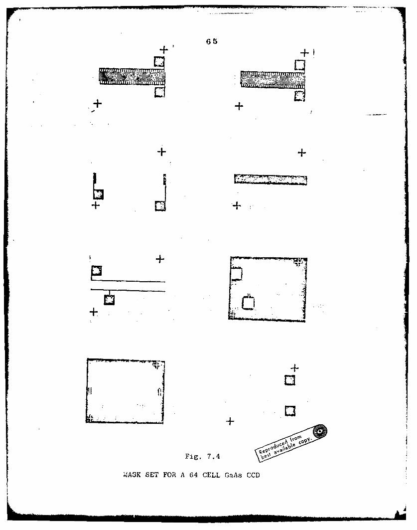
'353
-4S SETFORA 6 CLL aLsCC
66
APPENDIX I
AN AUTOMATI C C-V PLOTTER
-KBVIN E. FORWARD
4-+ HIDEKI HAS EGAWA
and
HANS L. * IA~RNAGEL
UNIVERSITY OF NO~ICASTLE UPON TYN5
Department of Electrical and Electronic Engineering1The kMerz Laboratories, Newcastle upon Tyne NE1 71W# U.K.
+ On leave from Honash Univormity, Victoria, Australia.
++ On leave from University of Hokkaido, Department. ofElectrical Engineering, Japan.

67
ABSTRACT
A C-V plotter is described which employs a novel
current sensing c.rcuit to enable the plotting of incremental
capacitance, do, as a function of bias 'oltage. The main
advantages off this current sensing circuit a're that the output
voltage, which is proportional to th, capacittive cur-rent thrnuga
the capacitor under test, i.s 'in phaz-,! with the-applied voltage
and t~hat its magnitude is inddpendent of frequency. The
product of these two terms at any sig~ial frequ-~ny therofor.3
contains a d.c. term which is p'roportional to -.he capacitance.
Design eqvations are ivnwbich enqble tis comtponcnts of
this circuit to be selected. Acomplete measurerint system
based on this circuit J- thea d~escribed and details of
particular c4: rcuitz- ar,, givenA. M-caples of plolts obtv-ined.
for GaAs MIS- _cb aditcrs are given as a iles of. the
a'l~ OZ of the s t .i

68
1. Introduction
According to Deal1 the study of insulator/semiconductorinterfaces is best carried out by means of C-V plots, and there
are many reports of the application of C-V plots to thedetermination of fast interface states, fixed charge and slow
trap densities (ref. 2' 3 4 , 6, for example). For therapid assessment of device processing which involves the use of
insulators on semiconductors an automatic C-V plotter is highlydesirable as manual methods such as point by point plotting
using a capacitance bridge tend to be tedious and timeconsuming. In designing such a system there are several
important -factora which must be considered to ensure that theinstrumcnt is versatile enough to permit those features of theC-V plots which ar' due to interface properties to bedistinguished from effects wl.ch are introduced by themoacuremont echniquo. The nub of this problem is that theeffects boirg c1se vcd are functions not only of bias voltage
but aloc of tin... The rate e change of the bias voltage is
therefore a criti'.Al fe.tor and consequently we have used aramp gcnorator, vith a rate controllable ove- a very widerangoo and have prov'.ded a hold feature which enables it to bestopp I at any point for quite long periods. -
The other ,actor which requires careful considerationis the amplitude and froquency of the small a.c. signalwhich ir urid to detect the incr mental or small signal
capccitanco. A5 tho stuey of fast interface state mequiresthe measurcr.-nt of Cnpnrwitc¢e i,.t widely differing frequenciesa novol ctnrrmto csi c',a.t hes been Covised which is
IW
independent of frequency but whIch still allows the test
capacqitor to be d.c. biased. This circuit is described in
detail below and an example is also given to show the
difference obtained by using,,- various frequencies when
measuring,11IS capacitors.
The capacitances to be measured are usu"-Ily quite
small and even small changes can be quite significant, so
that the system is required to have a relatively high
sensitivity. Some workers in tiis field have used the
variation ia detector current of a bri.dge circui ,t 'as an
isdicatiot. of h e change in capacitance, but-this is on-ly
Iitear over a limited ranv~e and is totally unr~aliable in
MSstudies', where, as Nicollian and Goetzbei-get poinr
out,' the c6nductance can vary much more rapidly than'the
capacitance. Another meThod wh~ich has. been propdsed by7* Tantk'apo~rA suffers from thae same disadvantage as
capacitive and conductive components are not distinguished
and has the added problem of having an output-,which is a'
.function of. freqiuency. We' 'have 'chosen a method. which eniab-les
a synchronous detector to be used, and which .has. an. outpufl.
independen*-of ,freque ncy. The synchronous detector ensures'
a high sensitivity ahd enables the capacitive-component td be
distinguished from tn.,e conductive Com.ponenL -,ensuring that the
variations obs~arved in the o~utput can reliably be interprtd
as variations in capacitanice.
A.- added advantage of' this system is that it is
extremely simple, due to the fct. that it can be realized xising
a few standard readil1y obtainable components.

70
2. Measurement System
Tantraporn has described a system for measuring
capacitance where a resi.tor is pliced in series with the
capacitor under test and the voltage across this resistor
is taken as proportional to the capacitance. The circuit
is shown in figure 1 and it can 1e seen by inspection that
provided R 4 l/C that the output voltage, vo, will be
given by
vu = vWC
Hence vo is directly proportioned to C but it also
varies with w. As pointed out above this circu. t also has
the disadvantage of not distinguishing between the
capacitance and the conductance and so is not suitable for
906 studies. The circuit in figire 2(a) shows a capacitor
in place of the resistor aad by inspection v0 is now given by
vos
provided Cs >>C. This circuit has two advantages: (1) it is
independent of frequency (2) vo and v are in phase if C is a
pure capacitance. When C is shunted by a conductance the
component of vo in phase with v is due to the capacitance and
independent of the shunting conduictance. The detection of
the in phase comp.)nent can be very simply achieved by
detecting the d.c. component of the product of v and vo .
Although the substitution oe C. for R enables C to be
easily detected, and removes the frequency dependence from the
output It eliminates the d.c. path by which the bias can be
applied to the test capacitor. A resistor R5 is therefore
k . . .. m m lm

7'
placed in parallel with C,, and provid- C R. >> l/WC S it will
not disturb v.. But R,. must also not disturb the d.c. bias
applied to C, so RS << a-.c., where RD.C is the d.c.
resistance of the test cap-acitor, is another inequality which
must also be satisfied. Figure 211b) shows a sam~pling circuit
which is completely satisfactcey provided the following
inequalitles are-satisfied:-
..a >> '-/,Cs (2)
* Re << RD.C (3)
In practice these inequalities are easily satisfied for high
qual'ity insulators such as are necessary in semiconductor
te~fizoiogies. As an exampl.e for C aSopr- and R%.C. >i10 1
CS - lOnF. and Rs 108 ohmns easily satisfy these requirements
while maintainin~g a measurement accuracy of better than 1%,
down to w as low at IOC rad.sec&1.
It has already 'jean stated above that the most
satisfactory detector for C is a ;.zultiplier with inputs v and
V 0 , so provided the r. mp is &pplied through a resistor R,
which.does. not attenuate the bmall signal voltage applied to
the-test capacit.or,a compleze syst6em for C-V measurement has
now been developed, and ---s shown ~nblocX diagram form in
figure .3. T~ae capacitor C1 ard C2 are provided to attenuate
the Wignai applied to the test capacitor so that the
measurement is Ynada with a suitu bl.y small voltage whilst
maintaining a svzbstantial sigaal at t!3e multi2lier input, ad
to isolate the d.c. bi as from th'e si Q2 enera7tor. The output
voltage fromn the current sam~pling c~ rCS requires

72
considerable amplificiticr. -nd, thWis can be carried out
by any high gain broad bancdwidth li-pass amplifier.
3. Circuit c'-n'ails
1The circui-ts -oq:. ro-X o realize the system
shown in figure 3 aro all. %V vzible in a variety
of integratod aaid d3i"-cre--. ncrj:-. ccuits, co the
Particular r ..... hr'c .;..Lo nl one of
an. izrZinite nL=nr o!7-.~iitc~ A1AW.-xoh re'* were- - -z..al ~ f:. 'qcencirc. from lO0flZ to Tu
and 1'e-nca desir-e:. <-r sy. ;- 'ri -aop'at- over t.-iat passaigeg
much hig qu'~tic-z'1 possilec. In Zatthe
ir, nocx. t , A Z~ a p'n-tL:ex% thee are rany
reacorbs -4 ke 1U nil' z-~mp ~rt hig!'kly desirable..Th- ce~t w i ~~r~ ae ~ir, to air.ly a step
ir.t t. .. z -~~ ~crl~~ cv? th,., step in V/
voltr nu,-*C) i' 0t. 4- 7 V. a-tr~~o:, ir. T then,,
thio o ,t-u4 i4-2- L. ~ 'VT~~~*~~~with a tin.
constant of At, 1 -- c or i~cen. cnd an input variable from0. 1 Volt t', 3 -,l r wArt ?oa10mv seJ-1
are possible. > zu . h-av3 uc-~d is3 shown in figure 4
wehere a. 74, !7p~~. ''i ro-"nrl. gain of 1O0is. h migSourco of 2n ii~i e the irt;Urtor. The single stage
output Tliir:.Kgt ~~' is pz'ovidedto enable anoutput swiria c" + C-- to~ !- c! tain-ad. Tho. d~ual - P.E.T.
usod in the in.-;at C'1317D tha' C13 .r- tofv t is small and
hence pruvi-A s a -7. :w'zift rato wl,,1"1,.~e inte!;raior is

73
switched to the hold position.
(B) Multiplier
An integrated Gilbert 10 multiplier which operates upto 156i"fI has been used and is the best of the multipliersZavaila1lee The potentiometers RV1 and RV2 are used to adjustthd'balanco and level of the output. An operational amplifier
has'ibien added as a level shifter and low pass filter.
Pinally, the output is filtered using a low pass passivefilter with a sharp cut-off at mains frequency to remove un-
wanted hiUm from the output. Figure 5 shows the multiplier,
output amplifier and filter.
(C) mlifier
We have used a four stage amplifier with a flat"Sponse up to 6MUi and a nominal midband gain of 750 which
ii stabilized by feedback applied to each stage,
Figure 6(a) shows some of the typical MIS curves we haveobtained for GaAs/(GaAs) oxide MOS system including the effect
of annealing, details of which have been reported by Hasegawa,
Forward and Hartnagel2. These curves show the wide range of
VALgnal frcquqnies, bias voltages and ramp rates which are
possible with this system. It is only fair to comment that
the bridge measurements required several hours of a skilled
operatorts time while the curves plotted automaticallyrequired only a few minutes.

74
S. Conclusion
A novel input circuit for a capacitance vs bias
voltage measurement system has boon described, which enables
measurements to be conveniently made over a wide frequencyrange. Provision has also been made for the application
of d.c. bias voltage and a sot of inequalities has been
given to enable the sampling capacitor and shunt resistorto be chosen. Circuits by which automatic C-V plotting
can be carried out using this input circuit have been Given.
Examples of its application to GaAs MIS capacitors are
provicLed, which show that this system is a most usefulinctrument in the study of MIS structures.
6 * Ai.-I-nodement
The authors wish to acknowledge the financialascist3nco of the U.S. Army European Research Office and the
Scicocc P.edebazoh Council of Groat Britain which made thiswork o ssible.
: R wr'nr *TCr;3
1. r I, B.E., J. 7lectr'ch,.. Soc. 121, 6, 198C, (1974).
2. Uaocrc.,a, H., Forward, K.'., Hartnagel, H.L.,
to be published.
3. ForbzsL., Yearenn, J.R., Keune, D.L., and Craford# M.G.Solid State Electronics jZ, 2S, (1974).
4. Foster, J.E., and Swartz, J.H., J. Electrochem. Soc.
11-7, 11, 1410, (1970).
5. Fahrner, W., J. Electrochem. Soc. 121, 6, 784-787 (1974).
6. Kern, W. and Whito, J.P.# R.C.A. Review Ll, 4,
771 (1970).
-75-
7. Tantraporn, W. J. Appi. Phys. 40,. 4665 (1969.).
8. Ikoma T. and Jeppson, B., 1972 International
Symposium on GaAs (1972).
9. Nicollian, E.H. and Goetzberger, A., J3.S.T.J. 46,
6, 1055 (1967).
10. Gilbert, B., IEEE, J. Solid State Circuits SC-3, 4,
p365-373 (1968).'

76
F'IGURZ CiAAP.!3C.TS
Figure 1.* Previous inpc.t cii-cuit 7
FiGure 2. Novelinpjut Circuit
Figure 3. B~1-f2 diaram of the co=.pleta system
Figure 4. Circuit diagUram of t*h-e rump generator
Pigure 5. Xultiylier, output cnplifio: and filter
Figure 6. =S.C-V plots by the 2resealt plotter as
successfully er-;.c-'yed to study effects
of aznea-ing on conodic native oxide of
Ga"s.
CO
qee \eCj%Oe\

7
PREVIOUS UNTUT CIRCUIT7
R v
Flgure 1

r
78
'-a.
p
0
0I-I
0.
0
1.4b3
a.
p
40

41
x* 79
4d4
C44
040
4Ar
U)q
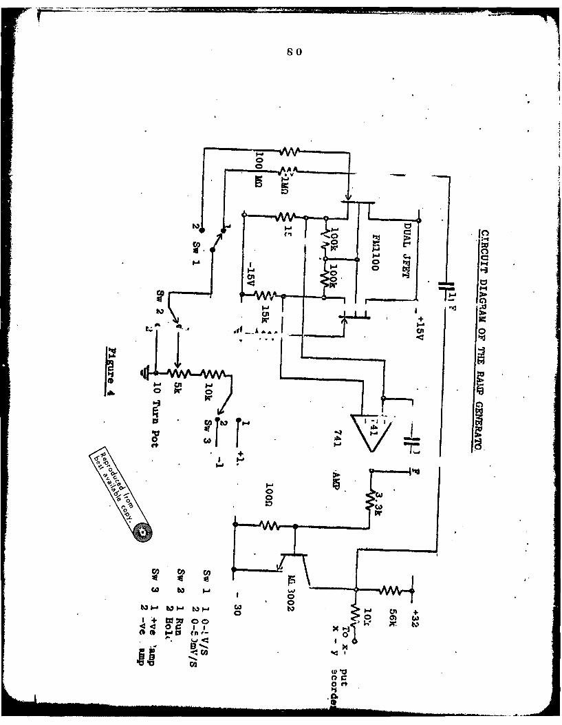
so
0- A4
I--3
w CA
0 coiC++
jCA,
co co ch
C b3 W Wt4
1+ W
00

P FJ84
OJN
14~
'A
&02F-tfc r*U) r-4
1-4l
oto> +1

riig
Ii 00I
/ /2
'-A /
/ z
,.. /1;/ j 2* /
-II
I /*1 ~-<~--"v_____I
o a-', /
I / ~ '-'JI
,~~:~ Li' -% ~.- / ..-.
~. %'st z* A,
S * 1/ //j*I 'I /j i.' /
* *" .11*1' ,/I~. jr/A, c~.
.4- 1/ f n
* ~.JLJW.J
-'-1 '~"a-.
~.4 ~
cJ -
*'~~ S.,
J* -~
~ ;~ ~A...
0,-~
II1 ~ N ~i
'-I ~ . S
Oi -~
ci -~
~ ~4.8K IQflimrft~1
~<
5.0 1/214 S
44

83
APPENJDIX. ir
LIST OF PUBLICATIONS
1. lartnagel, h., Singh, R., "New Method ofPassivating GaAs with AL20 3", presented at1974 International Electron Devices Meeting,Washington D.C., December 1974, TechnicalDigest p576.
2. Singh, R., Hartnagel, H., "Reduction inSurface Charge Density by New GaAs PassivationMethod", accepted for publication inJ. Phys. D, Letter.
3. Hasegawa, H., Forward, K.E., Hartnagel, H.,"An Improved Method of Anodic Oxidation ofGaAs", submitted for publication.
4. Hasegawa, H., Forward, K.E., Hartnagel, H.,"New Anodic Native Oxide of GaAs with ImprovedDielectric and Interface Properties",submitted for publication.
5. Forward, K.E., Hasegawa, H., Hartnagel, I.,"An automatic C-V Plotter", submitted forpublication.
uno|u~, lNruem.,.-,-- I ..J.