superlattices and microstructures - national chiao … addresses: [email protected] (r.b. kale),...
TRANSCRIPT

Superlattices and Microstructures 69 (2014) 239–252
Contents lists available at ScienceDirect
Superlattices and Microstructures
j o u r n a l h o m e p a g e : w w w . e l s e v i e r . c o m / l o ca t e / s u p e r l a t t i c es
Hydrothermal synthesis, characterizations andphotoluminescence study of single crystallinehexagonal ZnO nanorods with three dimensionalflowerlike microstructures
http://dx.doi.org/10.1016/j.spmi.2014.03.0030749-6036/� 2014 Elsevier Ltd. All rights reserved.
⇑ Corresponding authors. Tel.: +886 3 571464; fax: +886 3 5715408.E-mail addresses: [email protected] (R.B. Kale), [email protected] (S.-Y. Lu).
Rohidas B. Kale a,⇑, Yung-Jung Hsu b, Yi-Feng Lin c, Shih-Yuan Lu d,⇑a Department of Physics, Institute of Science, Mumbai 400032, MS, Indiab Department of Materials Science and Engineering, National Chiao Tung University, Hsinchu 30010, Taiwan, ROCc Department of Chemical Engineering and Materials Program, Chung Yuan Christian University, 200 Chung Pei Rd., Chung LiCity 32023, Taiwan, ROCd Department of Chemical Engineering, National Tsing-Hua University, Hsin-Chu 30013, Taiwan, ROC
a r t i c l e i n f o
Article history:Received 21 February 2014Received in revised form 24 February 2014Accepted 3 March 2014Available online 12 March 2014
Keywords:Hydrothermal methodMetal oxideX-ray diffractionScanning electron microscopeOptical properties
a b s t r a c t
A simple, low-cost, and environmentally benign hydrothermalapproach has been successfully developed to synthesize uniform,large-scale well-crystallized ZnO nanorods with different aspectratios that were united together to form three dimensional (3D)flowerlike structures. The method involved direct growth of ZnO3D microstructures using aqueous solution of Zn(CH3COO)2 asthe precursor and NaOH to adjust the pH of resultant solution. Sur-factants or templates were not used during the entire syntheticprocess. Moreover, the morphology evolution of the ZnO nanorodswith reaction time suggests a recrystallization–dissolution–growthmechanism that continuously takes place for prolonged interval oftime. The XRD pattern of the as-grown ZnO nanorods and relevantanalyses confirm the well crystallized hexagonal structure of theZnO microstructures and no evidence of any other impurity phases.SEM observations reveal that the ZnO product grew in the form ofnanorods that were united together to form 3D flowerlike mor-phology. The high resolution transmission electron microscopy(HRTEM) and selected area electron diffraction (SAED) shows thatthe ZnO nanorods were single crystalline and grew along the c-axisof the crystal plane. PL measurements of the as-synthesized nano-rods exhibit excellent excitation features and strong band-edge UV

240 R.B. Kale et al. / Superlattices and Microstructures 69 (2014) 239–252
luminescence even at room temperature. The uniform single crys-talline, defect free, and high aspect ratio nanorods may find prom-ising applications in optoelectronics and photo-catalysts. Thegrowth habit of ZnO crystal is also illustrated. This method is suit-able for large-scale production of ZnO microstructures and couldbe extended for syntheses of other metal oxides.
� 2014 Elsevier Ltd. All rights reserved.
1. Introduction
During the past decade, nanomaterials have drawn considerable research attentions, due to theirshape and size dependent structural and optoelectronic properties that differ from their bulk counter-parts [1–3]. In the present era, numerous researchers are actively engaged not only in syntheses butalso to control shape and size of nanostructures that includes nanowires, nanotubes, nanodiscs, nano-nails, nanobelts, nanocubes, nanoribbons, nanocables, nanorods, nanospheres and porous nanoscalematerials [4–10]. The smallest dimensional structures efficiently transport electrical carriers andmay find great applications in many areas, such as electronic, optoelectronic devices, and high perfor-mance photo-catalysts [10]. Also, shape and size of nanomaterial greatly affect the physicochemicalproperties that may be drastically different from those of their bulk counterparts [11]. Researchershave also demonstrated the correlation between the properties of nanomaterial and their morpholo-gies. As an example, ZnO nanorods exhibit improved near band edge emissions than porous nano-spheres [12]. The shape of Pt nanoparticles shows noticeable effects on the selectivity of benzenehydengenation [13]. SnO2 nanospheres with mesoporous structures have better electrochemical per-formances than the commercially available SnO2 samples [14]. It was observed that 2D nanowalls ofZnO have a higher transparency than 1D nanospike [15]. Among these numerous morphologies, con-trolled preparation of three-dimensional (3D) nanostructures composed of one dimensional nanoscalebuilding blocks, has stimulated extensive research attentions due to their enhanced physicochemicalproperties and superior device performances [16–20]. These hierarchical architectures combine thefeatures of nanoscale building units and can exhibit unique properties that are distinct from thoseof the low-dimensional structures. As stimulated by both the unique properties and promising appli-cations of such hierarchical architectures, great efforts have been focused on the design of rationalmethods to organize the nanoscale building blocks into complicated 3D microstructures.
Apart from numerous semiconductors, due to low-cost, environmental friendliness, easy to growand novel physicochemical properties. ZnO is exhaustively studied and gaining popularity as anintriguing candidate to be used for electronic and photonic devices [21]. It has a direct wide bandgap (3.37 eV) with a large exciton binding energy (60 meV), which can ensure sufficient exciton atroom temperature with an n-type conductivity and piezoelectric properties [22–25]. These promisingproperties make it an intriguing candidate to be used in various applications, such as dye sensitizedsolar cells, UV photon detectors, UV laser diodes, light emitting diodes, field emission displays, gassensors, active compounds in sunscreens, photo-catalysts, self-cleaning materials, energy harvestingdevices (nanogenerators), electronic devices (transistors), piezoelectric transducers, and actuators[26–34].
Previous studies also demonstrated that the properties of ZnO are closely related to the size andshape of the structures. For example, tetrapod ZnO nanostructures exhibit strong UV emissions [35]and needle-like ZnO arrays exhibit strong blue light emissions [36]. Thus, studying the morphologyof micro-nanostructure ZnO is an important research topic. As we know, the synthetic method andexperimental conditions greatly influence the morphology and/or shape as well as size of a nanoma-terial. Therefore, innovative synthetic methods or routes need to be developed for the control overmorphology, shape, and size. The most common method to synthesize one-dimensional ZnO nano-/microstructures is the vapor-phase transport process in the presence of metal catalysts,

R.B. Kale et al. / Superlattices and Microstructures 69 (2014) 239–252 241
microemulsion, thermal evaporation of Zn metal, and template-assisted growth [37–40]. However, theintroduction of templates to the reaction system makes the process more complicated and as a resultimpurity may be introduced in the final product. Moreover, the ZnO nanorods grown by the VLS pro-cess are usually interlinked together and form bundles with some junctions and defects that occur atelevated temperatures [41]. The poor dispersion of ZnO nanorods/nanowires synthesized by the VLSprocess may limit their practical applications [41]. Furthermore, preparation of one-dimensionalZnO macro-/nanostructures via solution growth processes without using templates provides a softand promising route for the large-scale production of uniform or well-dispersed macro-/nanostruc-tures of materials [42,43]. The ZnO nanorods and nanowires were synthesized earlier using micro-emulsion mediated hydrothermal processes [44,45]. However, it has disadvantages of ultrasonicpretreatment of the mixed solution and the usage of oil, chelating agents, and organic solvents, etc.which were adsorbed on the surface that affect the optical properties of the obtained ZnO nanorods.
Hydrothermal methods have attracted considerable attentions due to their mild reaction condi-tions, environmental benignancy, easy dispersion in liquid, pollution free, low cost, simplicity, highreaction rate, eco-friendliness, simplicity, low operating temperatures, large scale production, andeasy to control preparative parameters [46]. This method gives better control on the morphology aswell as size of the synthesized materials by changing the reaction conditions and the obtained productis of high crystalline in nature.
Previous reports are available on the hydrothermally synthesized 1D ZnO microstructures [47–50].However, non-uniform shape and size with poly-dispersed morphology were clearly seen. Hence,poly-disparity in morphology is still a challenging task during the growth of macro-/nanostructuresusing hydrothermal method. In the present study, we report on preparation of uniform flowerlike3D ZnO microstructures consisted of nanorod bundles with different aspect ratios, with a simplehydrothermal method, in the absence of unnecessary organic or inorganic additives, under mild con-ditions and low zinc concentrations. Subsequently, the influence of reaction time on the aspect ratio ofnanorods was also studied.
2. Experimental procedure
All the reagents were of analytical grade (purchased from Showa Chem. Co., Ltd., Japan) and usedwithout further purification. In a typical synthesis process, an appropriate amount of Zn(CH3COO)2
was dissolved in 50 ml (0.05 M) of deionized water (Milliq 18.2 MX) in a beaker. Then 50 ml (1 M)of aqueous solution of NaOH was added into it under constant stirring to get a clear aqueous solution.The pH of the resultant mixture was greater than 12. Then the resultant solution was transferred into aTeflon-container that was further sealed in a stainless steel autoclave. Finally, the autoclave was keptin a hot air oven and the temperature was maintained at 170 �C for 8, 16 and 24 h. After completion ofreaction, the autoclave was naturally cooled to room temperature. Subsequently, the resulting solidproduct was centrifuged, washed with distilled water and ethanol, finally dried at 80 �C in air and usedfor further characterizations.
The obtained samples were characterized by using different techniques. The crystallographic struc-ture and other relevant information related to structural determination were analyzed using an X-raydiffractometer (XRD, Mac Science, MXP18) with Cu Ka (k = 1.5406 Å) radiation over the range20� < 2h < 75�. The shape, size, and morphology of ZnO microstructures were characterized by usinga scanning electron microscope (SEM) (JEOL, JSM-5600) equipped with an energy dispersive X-rayanalyzer (EDXA, Oxford Instruments). A small drop of sample dispersed in ethanol was depositedon a carbon grid and then coated with gold (Au) layer for 30 s using an SEM sputter (SPI-Module Sput-ter Coating Unit, USA), before taking the SEM images. For TEM characterizations, ethanol dispersedsamples were deposited over a copper grid pre-coated with carbon. The transmission electron micro-scope (TEM) and electronic diffraction (ED) patterns were recorded on a JEOL JSM-2010 transmissionelectron microscope with an acceleration voltage of 200 kV. High-resolution electron microscope(HRTEM) images were obtained from a JEOL JEM-400EX operated at 400 kV. To study the optical prop-erties, optical absorption spectra were recorded using a UV–Visible spectrophotometer (Hitachi Mod-el-3300, Japan). Room temperature photoluminescence (PL) measurements were carried out using a

242 R.B. Kale et al. / Superlattices and Microstructures 69 (2014) 239–252
Hitachi F-4500 fluorescence spectrophotometer equipped with a xenon lamp (150 W) as the lightsource and photomultiplier (700 V) tube as a detector.
3. Results and discussions
XRD gives information about the crystalline phase, quality, orientation, composition, lattice param-eters, defects, stress, and strain of samples. Fig. 1 shows the XRD pattern of the ZnO microstructuresynthesized at 170 �C for 16 h and the standard card of bulk ZnO powders (PDF # 36-1451). All diffrac-tion peaks were indexed to a hexagonal wurtzite phase of ZnO, in agreement with the standard pat-tern. No characteristic peaks of any impurities were detected in the pattern, which confirms that theobtained products are pure ZnO. The comparison of the observed and the standard diffraction peakintensities does not show any preferred orientations. Also, it can be seen that the diffraction peaksare intensive and narrow that confirms the high crystalline nature of the as-synthesized ZnO micro-structures. Fig. 2 shows the XRD patterns of the ZnO microstructures obtained at 8 and 24 h. It clearlyreveals that the crystal growth of ZnO was not altered with increasing reaction time. It is also worthmentioning that the XRD peak positions of the 3D ZnO microstructures synthesized for 24 h matchesexactly with the standard JCPDS data. Only the peak positions of the sample synthesized at 8 h wereslightly shifted towards higher angles. It may be due to the initial nucleation and growth that contin-uously take place during the hydrothermal treatment.
Fig. 3(a) shows a representative EDAX pattern and the details of the relevant elemental analysis forthe ZnO microstructure (Inset shows the microstructure region that was used for the elemental anal-ysis). The pattern shows strong Zn and O peaks without any impurity peaks, confirming the purity ofthe observed ZnO microstructures. The average atomic percentage of the ZnO product is slightly richin oxygen for the sample synthesized at 8 h. It may be due to presence of some zinc hydroxide speciesin the sample that decomposes into ZnO in an extended time interval. The average atomic ratio for Znand O was found to be 1:1, indicating that the products synthesized at 16 and 24 h, were in good stoi-chiometric ratio. The peaks observed at 0.27 and 2.2 keV are of carbon (C) and gold (Au) due to thecarbon grid and gold sputtering, respectively.
Fig. 4(a and b) shows the SEM images of the ZnO product obtained at 170 �C for 8 h. SEM imagesclearly revealed that the numerous rods united together to form flowerlike three dimensional (3D)
Fig. 1. XRD pattern of ZnO microstructure synthesized with a reaction time of 16 h.

Fig. 2. XRD patterns of ZnO microstructures synthesized with a reaction time of (a) 8 h and (b) 24 h.
R.B. Kale et al. / Superlattices and Microstructures 69 (2014) 239–252 243
structures. The diameter of the nanorods is in the range of 300–500 nm and length is of the order of 6–8 lm. It is worth mentioning that a close observation reveals that some zinc hydroxide species arepresent at the base of the flowerlike microstructures and also in the surrounding region of the nano-rods that are decomposed into ZnO during prolonged time intervals. Also, the core of the microstruc-tures is somewhat bulky that will dissolve in due course of time and diffuse towards outer surfaces ofthe nanorods. It also reveals that the diameter is slightly thinner at the base of the nanorods and grad-ually increases (Fig. 4(b)) towards the end. Fig. 5(a and b) shows the SEM images of the ZnO productobtained for a 16 h reaction time. The morphology is more or less the same as that of the product syn-thesized for a 8 h reaction time. The lower magnification SEM images of ZnO revealed that the flow-erlike 3D structures are uniformly distributed over the grid surface and no evidence of poly-morphology. Furthermore, it is worth to mention that the diameter of the rod is in the range of300–400 nm, and the length is increased to 18–20 lm, with high aspect ratio of the order of 50. Suchhigh aspect ratio ZnO nanorods synthesized using a hydrothermal method has been scarcely reported.In addition to this, the diameter of the nanorods slightly but gradually decreases towards the end andthe surfaces of the rods are rounded curly. Fig. 6(a and b) shows the SEM images of the ZnO productobtained for a 24 h reaction time. It also reveals flowerlike 3D microstructure consisted of bunches ofnanorods with diameter �1 lm and length 6–8 lm. The SEM image clearly shows pronounced sharpsix faced prismatic microrods with flat top faces. Furthermore, the size of the rods tends to be uniformupon the erosion effect of extra base as reported [51]. The rods are bundled together with commoncrystallographic faces coalescing together due to oriented attachment to lower the surface area andto minimize the surface energy for thermodynamic stability. The oriented attachment mechanism de-scribes the spontaneous self-organization of adjacent particles, so that they share a common crystal-lographic orientation, followed by the joining of these particles at a planar interface. The decrease inlength of the rods can be explained in terms of growth kinetics, by which the fastest growing planesshould disappear to leave behind the slowest growing planes as the facets of the product [52]. It is dueto the fact that the fastest growing polar surfaces will be dissolved preferentially since this decreases

Fig. 3. EDAX pattern of the ZnO microstructures synthesized with reaction time of (a) 8 h (b) 16 h and (c) 24 h (insets shows theelemental analysis and region selected for it).
244 R.B. Kale et al. / Superlattices and Microstructures 69 (2014) 239–252
the system energy during further consequent aging process, and that progressively, leads to the for-mation of ZnO rods with sharp top surface. Growth morphology is also highly sensitive to the level

Fig. 4. SEM images of 3D flowerlike ZnO microstructures synthesized with reaction time of 8 h (a) low magnification and (b)high magnification.
R.B. Kale et al. / Superlattices and Microstructures 69 (2014) 239–252 245
of super-saturation. It has been suggested that precipitation should follow the order of sulfate, nitrate,chloride and acetate. Empirical observations followed the order of sulfate, chloride, nitrate, formateand acetate anion. The induction period for baths containing acetate was significantly longer thanfor baths containing the other salts [53].
In the present hydrothermal conditions, we have synthesized flowerlike ZnO microstructures bythe direct decomposition of soluble Zn(OH)4
2� precursor, which follows the growth habit of the ZnOcrystals. The crystal growth process involves the following four stages: nucleation, crystal growth, dis-solution and recrystallization. Experimental conditions not only affect on the morphology but also onthe size of a growing crystal, in which numerous factors integrate to dominate the process. The behav-ior of crystal growth depends on the aggregation that takes place in the initial induction period andthe subsequent growth, diffusion, dissolution, and recrystallization processes. As we know, duringthe initial reaction period, reaction time affects on the overall size of the aggregation rather than thatof the morphology. Subsequent depletion in reactant concentration during a further extension of reac-tion time, the effects of growth, dissolution and recrystallization processes affect the overall size andmorphology.
The formation process of ZnO in aqueous solution is generally suggested through the followingreactions:
Zn2þ þ 2ðOHÞ� ! ZnðOHÞ2 ð1Þ

Fig. 5. SEM images of 3D flowerlike ZnO microstructures synthesized with reaction time of 16 h (a) low magnification and (b)high magnification.
246 R.B. Kale et al. / Superlattices and Microstructures 69 (2014) 239–252
ZnðOHÞ2 þ 2OH� ! ZnðOHÞ42� ð2Þ
ZnðOHÞ2�4 ! ZnOþH2Oþ 2OH� ð3Þ
At the initial stage, when limited amount of aqueous alkaline NaOH solution was added, whiteZn(OH)2 precipitates were obtained. Further addition of excess sodium hydroxide into the solutionhowever led to the re-dissolution of Zn(OH)2 precipitates to form a homogeneous solution containingZn(OH)4
2� ions that played a key role in the morphology development of the ZnO crystallites. With theincrease in temperature above 160 �C, along with the autogenously generated pressure developed in-side the autoclave, the preformed Zn(OH)4
2� ions decomposed to ZnO nanoparticles that acts as seednuclei. Thus, at the early stage of the reaction, the product was composed of ZnO nuclei that were sur-rounded by abundant Zn(OH)4
2�. At higher concentration of NaOH (1 M) the nucleation followed bycrystal growth was relatively fast that resulted in formation of abundant ZnO nanoparticles. Thus atthe early stage, ZnO nuclei and growth species of Zn(OH)4
2� coexisted in equilibrium. These preformedZnO nanoparticles were highly unstable and quickly aggregated into bigger aggregates to minimizethe surface energy. In addition, soluble species of Zn(OH)4
2� deposited on the solid surfaces of pre-formed ZnO nanoparticles. After that, ZnO nanoparticles grew to a stable size, and they continuedto grow further by combining with smaller unstable nuclei [54]. Subsequent to this growth, relativelylarger particles formed on the surface of the aggregates, smaller and poorly-crystallized nanoparticleswere included at the core of the aggregates [55]. Due to the high surface energy of the smaller nano-

Fig. 6. SEM images of 3D flowerlike ZnO microstructures synthesized with reaction time of 24 h (a) low magnification and (b)high magnification.
R.B. Kale et al. / Superlattices and Microstructures 69 (2014) 239–252 247
particles, that were present in the cores, these smaller nanoparticles can dissolve easily and diffuseoutwards. The large nanoparticles located on the surfaces of the bigger aggregates served as the start-ing growth sites for the subsequent recrystallization process and crystal growth continued [56]. Dur-ing this process, a rupture of the initial homogeneous nucleation occurred and the growth units weredirectly incorporated into ZnO crystallites under the present experimental conditions. As the reactiontime increased, the concentrations of Zn2+ and OH� gradually decreased and the depletion of thesespecies favored the diffusion, dissolution, and recrystallization processes. These processes dominatedonly in the latter stage of the morphology evolution during the reforming period, when raw materialsbecame scarce. Thus, during the initial reaction period, the reaction time affects the overall size of theaggregates instead of the morphology. But, when the reactant concentration decreased gradually dur-ing the prolonged reaction time period, the effects of diffusion, dissolution, and recrystallization pro-cesses affected the overall morphology of the synthesized products. These processes were sensitive tothe pH of the reaction mixture, reaction temperature, and autogenously generated pressure [56].
According to the growth habit of ZnO crystals, the relative rates of the ZnO crystal growth in dif-ferent directions have been V(0001)>Vð0111Þ > Vð0110Þ > Vð00001Þ reported [57]. Hence, growthunits were preferentially supplied for the c-axis direction of every nucleus, which caused the genera-tion of numerous randomly distributed ZnO nanorods. Hence, during the diffusion, dissolution, andrecrystallization processes, numerous nanorods were grown on the bigger aggregates surfaces dueto the preferential attachment of growth units along the c-axis, leading to the formation of hierarchicalbundle-like architectures. Also, because of the gradual mass diffusion from the inner core to the out-

248 R.B. Kale et al. / Superlattices and Microstructures 69 (2014) 239–252
ermost surface, the rods located on the outer surface grew in length at the expense of the dissolvedcore materials. Finally, after prolonging the reaction further, the inner cores were consumed com-pletely and the typical flowerlike microstructures assembled with several nanorods were formed[58]. The oriented growth attachment became pronounced after the prolonged time interval. The sche-matic presentation of the possible growth mechanism of the flowerlike ZnO nanorods is shown inFig. 7. To support the growth mechanism that is illustrated in Fig. 7, the ZnO product was also synthe-sized for short reaction periods (4 h) and the SEM image is depicted in Fig. 8. It clearly reveals theaggregation of ZnO nanoparticles, and the numerous bursts originated from the aggregations.
The detailed structural and morphological characterizations of the as-grown ZnO nanorods synthe-sized for 16 h were also done by TEM and HRTEM equipped with SAED. Fig. 9(a) shows the low-mag-nification TEM image of the as-grown ZnO nanorods, which is in full agreement with the SEM image interms of their dimensionality. The SAED pattern of the corresponding nanorod is shown in Fig. 9(b),confirming that the grown nanorods are single crystalline with the wurtzite hexagonal phase and
Fig. 7. Schematic representation for the formation of 3D flowerlike ZnO microstructures.
Fig. 8. SEM image of ZnO microstructures synthesized with a reaction time of 4 h.

R.B. Kale et al. / Superlattices and Microstructures 69 (2014) 239–252 249
grown along the (0001) direction. HRTEM image of the nanorod displayed in Fig. 9(a) is shown inFig. 9(c), which clearly shows well-defined lattice fringes. The distances between two parallel latticefringes were measured to be about�0.259 nm, which corresponds to the spacing of the (0001) crystalplanes of ZnO with wurtzite hexagonal phase and confirming that the as-grown nanorods are single-crystalline with the wurtzite hexagonal phase and grown along the (0001) direction. The results re-vealed from the SAED pattern and HRTEM image of the ZnO nanorods are consistent with each otherand confirm the single crystalline nature of the nanorods and their growth along the c-axis.
It is commonly known that the room-temperature PL spectra for ZnO usually shows four majorpeaks: a UV emission peak around 380 nm, a blue emission peak around 440–480 nm, a green emis-sion peak around 520 nm, and a red or orange emission peak around 600 nm [59]. The UV peak isattributed to the near band-edge emission, while the other three broad visible bands are generallyattributed to the de-excitation process related to defects states in ZnO crystal, such as vacanciesand interstitials of zinc and oxygen [60]. Fig. 10 shows the room temperature PL spectra of the ZnO
Fig. 9. (a) TEM, (b) SAED and (c) HRTEM image of ZnO nanorod synthesized for 16 h.
Fig. 10. Room-temperature photoluminescence spectrum of ZnO microstructures synthesized for 16 h.

250 R.B. Kale et al. / Superlattices and Microstructures 69 (2014) 239–252
microstructure under different excitation wavelength. The room temperature PL spectra reveal highlyintense peaks centered at 395, 397, and 399 nm (kexc = 325, 300, and 275 nm)) that correspond to theUV emission. The intense UV emission band is explained by a near band edge transition of the wideband gap ZnO nanorods, namely the recombination of free exciton through an exciton–exciton colli-sion process [61]. The absence of the emission peaks due to impurities and defects in the present syn-thesized ZnO nanorods indicates excellent optical property free from any defects that are commonlyobserved for products from hydrothermal syntheses. The PL intensities were found to increase withnarrowing FWHM by decreasing the excitation wavelength and the results are in agreement with ear-lier reports [62]. Previous researchers observed that the PL peaks of ZnO are red-shifted [63,64] withincreasing excitation wavelengths. In the present study, no significant red shifts in peaks positionwere observed with changes in excitation wavelength.
Fig. 11(a and b) shows the SEM images of ZnO microstructures synthesized for 18 h, when the com-plex reagent NaOH was replaced with NH4OH, so that the pH of the reaction mixture was�10, withoutdisturbing other experimental conditions. It clearly reveals the formation of interesting flowerlike 3Dstructures composed of numerous nanorods with sharp prismatic hexagonal surfaces. It also clearlyreveals the existence of polar surfaces with sharp tip of the (0001) plane. The nanorods with sharpand narrow tip are the intriguing candidates for lasing action. It clearly divulges that the complex re-agent plays an important role and affects the growth habit of the ZnO nanorods. The schematic rep-resentation for growth habit of ZnO crystal under present experimental conditions is shown in Fig. 12.
Fig. 11. SEM images of 3D flowerlike ZnO microstructures synthesized for 16 h using NH4OH (a) low magnification and (b) highmagnification.
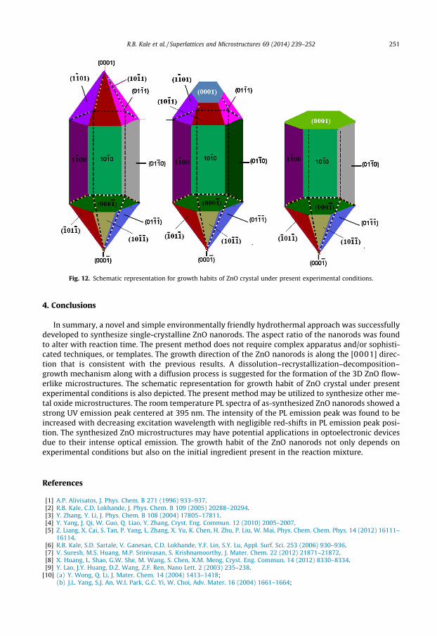
Fig. 12. Schematic representation for growth habits of ZnO crystal under present experimental conditions.
R.B. Kale et al. / Superlattices and Microstructures 69 (2014) 239–252 251
4. Conclusions
In summary, a novel and simple environmentally friendly hydrothermal approach was successfullydeveloped to synthesize single-crystalline ZnO nanorods. The aspect ratio of the nanorods was foundto alter with reaction time. The present method does not require complex apparatus and/or sophisti-cated techniques, or templates. The growth direction of the ZnO nanorods is along the [0001] direc-tion that is consistent with the previous results. A dissolution–recrystallization–decomposition–growth mechanism along with a diffusion process is suggested for the formation of the 3D ZnO flow-erlike microstructures. The schematic representation for growth habit of ZnO crystal under presentexperimental conditions is also depicted. The present method may be utilized to synthesize other me-tal oxide microstructures. The room temperature PL spectra of as-synthesized ZnO nanorods showed astrong UV emission peak centered at 395 nm. The intensity of the PL emission peak was found to beincreased with decreasing excitation wavelength with negligible red-shifts in PL emission peak posi-tion. The synthesized ZnO microstructures may have potential applications in optoelectronic devicesdue to their intense optical emission. The growth habit of the ZnO nanorods not only depends onexperimental conditions but also on the initial ingredient present in the reaction mixture.
References
[1] A.P. Alivisatos, J. Phys. Chem. B 271 (1996) 933–937.[2] R.B. Kale, C.D. Lokhande, J. Phys. Chem. B 109 (2005) 20288–20294.[3] Y. Zhang, Y. Li, J. Phys. Chem. B 108 (2004) 17805–17811.[4] Y. Yang, J. Qi, W. Guo, Q. Liao, Y. Zhang, Cryst. Eng. Commun. 12 (2010) 2005–2007.[5] Z. Liang, X. Cai, S. Tan, P. Yang, L. Zhang, X. Yu, K. Chen, H. Zhu, P. Liu, W. Mai, Phys. Chem. Chem. Phys. 14 (2012) 16111–
16114.[6] R.B. Kale, S.D. Sartale, V. Ganesan, C.D. Lokhande, Y.F. Lin, S.Y. Lu, Appl. Surf. Sci. 253 (2006) 930–936.[7] V. Suresh, M.S. Huang, M.P. Srinivasan, S. Krishnamoorthy, J. Mater. Chem. 22 (2012) 21871–21872.[8] X. Huang, L. Shao, G.W. She, M. Wang, S. Chen, X.M. Meng, Cryst. Eng. Commun. 14 (2012) 8330–8334.[9] Y. Lao, J.Y. Huang, D.Z. Wang, Z.F. Ren, Nano Lett. 2 (2003) 235–238.
[10] (a) Y. Wong, Q. Li, J. Mater. Chem. 14 (2004) 1413–1418;(b) J.L. Yang, S.J. An, W.I. Park, G.C. Yi, W. Choi, Adv. Mater. 16 (2004) 1661–1664;

252 R.B. Kale et al. / Superlattices and Microstructures 69 (2014) 239–252
(c) Z.R. Tian, J.A. Voigt, J. Liu, B. McKenzie, M.J. McDermott, M.A. Rodriguez, H.K. Xu, Nat. Mater. 2 (2003) 821–826;(d) G. Wang, D. Chen, H. Zhang, J.Z. Zhang, H.J. Li, J. Phys. Chem. C 112 (2008) 8850–8855.
[11] C.Z. Wen, H.B. Jiang, S.Z. Qiao, H.G. Yang, G.Q. Lu, J. Mater. Chem. 21 (2011) 7052–7061.[12] G. Yuan, J. Zhu, C. Li, X. Gao, Cryst. Eng. Commun. 14 (2012) 7450–7457.[13] I. Lee, F. Delbecq, R. Morales, M.A. Albiter, F. Zaera, Nat. Mater. 8 (2009) 132–138.[14] R.D. Cakan, Y.S. Hu, M. Antonietti, J. Maier, M.M. Titirici, Chem. Mater. 20 (2008) 1227–1229.[15] D. Pradhan, K.T. Leung, Langmuir 24 (2008) 9707–9716.[16] H.B. Wu, J.S. Chen, X.W. Lou, H.H. Hng, J. Phys. Chem. C 115 (2011) 24605–24610.[17] S. Baruah, J. Dutta, Sci. Technol. Adv. Mater. 10 (2009) 013001–0130018.[18] Z.M. Chen, H. Cao, C.W. Hu, J. Phys. Chem. C 115 (2011) 5522–5529.[19] Y. Li, Z.J. Si, Y.Q. Lei, X.N. Li, J.K. Tang, S.Y. Song, H.J. Zhang, Cryst. Eng. Commun. 13 (2011) 642–648.[20] X.L. Cheng, J.S. Jiang, M. Hu, G.Y. Mao, F.X. Bu, C.C. Lin, Y. Zeng, Q.H. Zhang, Cryst. Eng. Commun. 14 (2012) 7701–7708.[21] D.C. Look, B. Clafin, Y.J. Alivov, S.J. Park, Phys. Status Solidi A 201 (2004) 2203–2212.[22] J. Bae, J.B. Han, X.M. Zhang, M. Wei, X. Duan, Y. Zhang, Z.L. Wang, J. Phys. Chem. C 113 (2009) 10379–10383.[23] Y. Sun, G.M. Fuge, N.A. Fox, D.J. Riley, M.N.R. Ashfold, Adv. Mater. 17 (2005) 2477–2481.[24] Y. Qin, X.D. Wang, Z.L. Wang, Nature 451 (2008) 809–813.[25] X.D. Wang, J.H. Song, J. Liu, Z.L. Wang, Science 316 (2007) 102–105.[26] Q. Zhang, C.S. Dandeneau, X. Zhou, G. Cao, Adv. Mater. 21 (2009) 4087–4108.[27] C.Y. Lu, S.J. Chang, S.P. Chang, C.T. Lee, C.F. Kuo, H.M. Chang, Y.Z. Chiou, C.L. Hsu, I.C. Chen, Appl. Phys. Lett. 89 (2006)
153101–153103.[28] B.S. Zou, R. Liu, F. Wang, A. Pan, L. Cao, Z.L. Wang, J. Phys. Chem. B 110 (2006) 12865–12873.[29] S.H. Park, S.H. Kim, S.W. Han, Nanotechnology 18 (2007) 055608.[30] G. Kenanakis, D. Vernardou, N. Katsarakis, Appl. Catal. A: General 411–412 (2012) 7–14.[31] V.R. Shinde, T.P. Gujar, C.D. Lokhande, Sens. Actuators B: Chem. 120 (2007) 551–559.[32] X.D. Bai, E.G. Wang, P.X. Gao, Z.L. Wang, Nano Lett. 3 (2003) 1147–1150.[33] X.Y. Kong, Z.L. Wang, Nano Lett. 3 (2003) 1625–1631.[34] A.B. Djuri, X. Chen, Y.H. Leung, A.M. Ching, Ng, J. Mater. Chem. 22 (2012) 6526–6535.[35] Z.G. Chen, A.Z. Ni, F. Li, H.T. Cong, H.M. Cheng, G.Q. Lu, Chem. Phys. Lett. 434 (2007) 301–395.[36] T.G. You, J.F. Yan, Z.Y. Zhang, J. Li, J.X. Tian, J.N. Yun, W. Zhao, Mater. Lett. 66 (2012) 246–249.[37] A. Ishizumi, Y. Kanemitsu, Appl. Phys. Lett. 86 (2005) 253106–253109.[38] Z.R. Dai, Z.W. Pan, Z.L. Wang, Adv. Funct. Mater. 13 (2003) 9–24.[39] A. Umar, B.K. Kim, J.J. Kim, Y.B. Hahn, Nanotechnology 18 (2007) 175606.[40] S.T. Lee, C.H. Liu, J.A. Zapien, Y. Yao, X.M. Meng, C.S. Lee, S.S. Fan, Y. Lifshitz, Adv. Mater. 15 (2003) 838–841.[41] J. Wang, L. Gao, J. Mater. Chem. 13 (2003) 2551–2554.[42] X. Wang, Y.D. Li, J. Am. Chem. Soc. 41 (2002) 2446–2461.[43] T. Kasuga, M. Hiramatsu, A. Hoson, T. Sekino, K. Nihara, Adv. Mater. 11 (1999) 1307–1311.[44] J. Zhang, L. Sun, H. Pan, C. Liao, C. Yan, New J. Chem. 26 (2002) 33–34.[45] J.C. Lin, C.P. Lee, K.C. Ho, J. Mater. Chem. 22 (2012) 1270–1273.[46] H. Wang, J.K. Xiey, Y.M. Duan, J. Mater. Sci. Technol. 27 (2011) 153–158.[47] R.B. Kale, S.Y. Lu, J. Phys.: Condens. Matter 19 (2007) 096209.[48] Y. Wang, Z. Hou, H. Guo, L. Shen, G.F. Wang, Q. Zhang, Mater. Lett. 91 (2013) 107–110.[49] N. Kiomarsipour, R.S. Razavi, Superlattices Nanostruct. 52 (2012) 704–710.[50] P.K. Giri, S. Bhattacharya, B. Chetia, S. Kumari, D.K. Singh, P.K. Iyer, J. Nanosci. Nanotechnol. 11 (2011) 1–6.[51] Q.Q.P. Ding, Q.Q. Cao, H.B. Huang, S.G. Yang, X.N. Zhao, Y.W. Du, J. Phys. D: Appl. Phys. 39 (2006) 46–49.[52] Z.L. Wang, J. Phys. Chem. B 104 (2000) 1153–1175.[53] K. Govender, D.S. Boyle, P.B. Kenway, P. O’Brien, J. Mater. Chem. 14 (2004) 2575–2591.[54] H. Colfen, S. Mann, Angew. Chem. Int. Ed. 42 (2003) 2350–2365.[55] (a) B. Liu, H.C. Zeng, Small 1 (2005) 566–571;
(b) X.X. Yu, J.G. Yu, B. Cheng, B.B. Huang, Chem. Eur. J. 15 (2009) 6731–6739;(c) W. Cheng, K.B. Tang, Y.X. Qi, J. Sheng, Z.P. Liu, J. Mater. Chem. 20 (2010) 1799–1805.
[56] J. Zhang, L. Sun, J.L. Yin, H. Su, C. Liao, C. Yan, Chem. Mater. 14 (2002) 4172–4177.[57] A. Smith, R. Rodrıguez-Clemente, Thin Solid Films 345 (1999) 192–196.[58] X.L. Cheng, J.S. Jiang, M. Hu, G.Y. Mao, F.X. Bu, C.C. Lin, Y. Zeng, Q.H. Zhang, Cryst. Eng. Commun. 14 (2012) 7701–7708.[59] S.A. Studenikin, N. Golego, M.J. Cocivera, Appl. Phys. 84 (1998) 2287–2294.[60] (a) X. Liu, X. Wu, H. Cao, R.P.H. Chang, J. Appl. Phys. 95 (2004) 3141–3147;
(b) W.J. Qin, J. Sun, J. Yang, X.W. Du, Mater. Chem. Phys. 130 (2011) 425–430;(c) R.N. Bhargava, D. Gallagher, X. Hong, A. Nurmikko, Phys. Rev. Lett. 72 (1994) 416–419;(d) A.G. Joshi, S. Soanl, N. Gandhi, Y.G. Radha Krishna, D. Haranath, Appl. Phys. Lett. 96 (2010) 123102–123104;(e) W.M. Huang, P. Jiang, C.Y. Wei, D.K. Zhuang, J.L. Shi, J. Mater. Res. 23 (2008) 1946–1952.
[61] Y.C. Kong, D.P. Yu, B. Zhang, W. Fang, S.Q. Feng, Appl. Phys. Lett. 78 (2001) 407–409.[62] P. Zhang, L.J. Gao, Colloid Interface Sci. 266 (2003) 457–460.[63] L. Irimpan, B. Krishnan, A. Deepthy, V.P.N. Nampoori, P. Radhakrishnan, J. Phys. D: Appl. Phys. 40 (2007) 5670–5674.[64] F. Khan, S. Ameen, M. Song, S.H. Shin, J. Lumin. 134 (2013) 160–164.