study of self-heating effects in gan hemts by towhid ......study of self-heating effects in gan...
TRANSCRIPT

Study of Self-Heating Effects in GaN HEMTs
by
Towhid Chowdhury
A Thesis Presented in Partial Fulfillment of the Requirements for the Degree
Master of Science
Approved May 2013 by the Graduate Supervisory Committee:
Dragica Vasileska, Chair
Stephen Goodnick Michael Goryll
ARIZONA STATE UNIVERSITY
August 2013

i
ABSTRACT
GaN high electron mobility transistors (HEMTs) based on the III-V nitride material
system have been under extensive investigation because of their superb performance as
high power RF devices. Two dimensional electron gas(2-DEG) with charge density ten
times higher than that of GaAs-based HEMT and mobility much higher than Si enables a
low on-resistance required for RF devices. Self-heating issues with GaN HEMT and lack
of understanding of various phenomena are hindering their widespread commercial
development. There is a need to understand device operation by developing a model
which could be used to optimize electrical and thermal characteristics of GaN HEMT
design for high power and high frequency operation.
In this thesis work a physical simulation model of AlGaN/GaN HEMT is developed
using commercially available software ATLAS from SILVACO Int. based on the energy
balance/hydrodynamic carrier transport equations. The model is calibrated against
experimental data. Transfer and output characteristics are the key focus in the analysis
along with saturation drain current. The resultant IV curves showed a close
correspondence with experimental results. Various combinations of electron mobility,
velocity saturation, momentum and energy relaxation times and gate work functions were
attempted to improve IV curve correlation. Thermal effects were also investigated to get
a better understanding on the role of self-heating effects on the electrical characteristics
of GaN HEMTs. The temperature profiles across the device were observed. Hot spots
were found along the channel in the gate-drain spacing. These preliminary results
indicate that the thermal effects do have an impact on the electrical device characteristics
at large biases even though the amount of self-heating is underestimated with respect to

ii
thermal particle-based simulations that solve the energy balance equations for acoustic
and optical phonons as well (thus take proper account of the formation of the hot-spot).
The decrease in drain current is due to decrease in saturation carrier velocity. The
necessity of including hydrodynamic/energy balance transport models for accurate
simulations is demonstrated. Possible ways for improving model accuracy are discussed
in conjunction with future research.

iii
Dedicated to my beloved parents

iv
ACKNOWLEDGMENTS
Several individuals played an important role whose sincere help made me complete this
thesis. I would first like to thank Professor Dr. Dragica Vasileska for her ample support
in giving direction to my research, keeping the thesis on track, ensuring the quality of
final result and helping me in exploring the exciting challenging world of TCAD
simulations. I would like to thank my Graduate Supervisory Committee members
Professor Dr. Stephen M. Goodnick and Professor Dr. Michael Goryll for providing me
useful information regarding my research. Late Dr. Dieter Schroder had helped me
develop a better understanding of device physics theory by always being readily available
to answer my questions. He has been also an inspiration for me to take up the field of
solid state devices as a field of career. I would like to thank the group members of
Professor Dr. Dragica Vasileska in providing guidelines to edit my thesis and also
provide stimulating discussions on the physics of the device(Balaji Padmanabhan).
I thank my parents for their devotion in raising me and being a great support for me all
during these several months of hard work.

v
TABLE OF CONTENTS
Page
LIST OF TABLES……………………………………………………………………….vii
LIST OF FIGURES………………………………………………………………………ix
CHAPTER
1.INTRODUCTION………………………………………………………………….1
1.1. Overview………………………………………………………………………1
1.2. History of GaN Devices……………………………………………………….3
1.3. Piezoelectric and Spontaneous Polarization…………………………………..6
1.4.Thermal Issues of AlGaN/GaN HEMT……………………………………….11
1.5. Motivation for this work and Approach…...…………………………………17
2. DEVICE MODELING AND SIMULATION…………………………………….19
2.1.Semiconductor Device Simulations ................................................................. 19
2.1.1. Importance of Simulation………………………………………………19
2.1.2. General Device Simulation Framework.................................................. 19
2.2. SILVACO…………………………………………………………………….20
2.3. Device Structure.............................................................................................. 23
2.3.1. AlGaN/GaN HEMT ................................................................................ 24
2.3.2. GaN/AlGaN/AlN/GaN HEMT ............................................................... 25
2.4. Physical and Material Models .......................................................................... 26
2.4.1.Drift-Diffusion(DD)Transport Model(Homogenous Structure).………..27
2.4.2.Drift-diffusion with Position Dependent Band Structure ........................ 30
2.4.3. Hydrodynamic(Energy balance) Transport Model……………………..32

vi
CHAPTER Page
2.4.4. Hydrodynamic Boundary Condition ....................................................... 37
2.4.5. Boundary Physics: Ohmic and Schottky Contact………………………37
2.4.5.1. Ohmic Contacts...………………………………………………..38
2.4.5.2. Schottky Contact………………………………………………..38
2.4.6. Mobility Model…………………………………………………………39
2.4.7. Piezoelectric and Spontaneous Polarization Implementation………......43
2.5. Self-heating Simulations..………………………………………………….. 44
2.5.1. Overview………………………………………………………………..44
2.5.2. Numerics………………………………………………………………..44
2.5.3.Non-Isothermal Models…………………………………………………45
2.5.3.1. Lattice Heat Flow Equation…………………………………….45
2.5.3.2. Effective Density of States………………………………………46
2.5.3.3. Non-Isothermal Current Densities………………………………46
2.5.3.4. Heat Generation…………………………………………………48
2.5.3.5. Thermal Boundary Condition.……………………………..........51
2.6. Gummel’s Iteration Method………………………………………………….52
2.7. Model Development………………………………………………………….53
2.8. Importance of Use of Hydrodynamic Transport Model……………………...55
3. SIMULATION RESULTS………………………………………………………57
3.1. AlGaN/GaN HEMT .................................................................................... …57
3.1.1. Isothermal Simulation ......................................................................... …57
3.1.1.1. Transfer Curve…………………………………………………...57

vii
CHAPTER Page
3.1.1.2. Output I-V Curve...........................................................................58
3.1.2. Thermal Simulation…………………………………………………...59
3.1.2.1. Transfer Curve………………………………………………….59
3.1.2.2. Output I-V Curve………………………………………………..61
3.1.2.3. Temperature and Joule Heating Profile………………………....63
3.2. GaN/AlGaN/AlN/GaN HEMT .................................................................... ..65
3.2.1. Isothermal Simulation………………………………………………......65
3.2.1.1. Transfer Curve………………......................................................65
3.2.1.2. Output I-V Curve…………………………………………...........66
3.2.2. Non-Isothermal Simulation ............................................................... ….67
3.2.2.1. Transfer Curve……………………………………………..........67
3.2.2.2. Output I-V Curve………………………………………………...68
3.2.2.3. Temperature and Joule Heating Profile………………………….69
4. CONCLUSIONS AND FUTURE WORK……………………………………….72
4.1. Conclusions ...................................................................................................... 72
4.2. Future Work………………………………………………………………….73
REFERENCES……. ................................................................................................…….76

viii
LIST OF TABLES
Table Page 1.1 Semiconductor material properties at 300K………………………………………..1
1.2 Mobility and the corresponding temperature ........................................................... 13
1.3 Thermal conductivities of popular substrate materials…………………………….17
2.1 User definable parameters in field-dependent mobility model……………………43

ix
LIST OF FIGURES
Figure Page
1.1 TEM crosssection of MOCVD grown GaN on SiC substrate using AlN buffer
layer(left) and LEO grown GaN (right)......................................................................5
1.2 Field-Plated Device Structure ................................................................................... 5
1.3 IV characteristics showing knee walk-out .................................................................. 6
1.4 Crystal structure of wurtzite Ga-face and N-face Gallium Nitride.. ...................... ..…7
1.5 Spontaneous and Piezoelectric polarization charge and their direction in Ga-faced
and N-faced strained and relaxed AlGaN/GaN HEMT................................................9
1.6 Low-field mobility µo (cm2/Vs)variation with sheet carrier concentration
ns(cm-3)……………………………………………………………………………..13
1.7 Dependence of low-field mobility µo (cm2/Vs) on temperature T(K)……………...14
1.8 Inverse thermal conductivity 1/K(Tsub) (cm K/W) variation with temperature T(K)
for different substrate materials…………………………………….......................16
2.1 Schematic description of the device simulation sequence…………………………………………20
2.2 Representation of ATLAS’ modular structure…………………………...................21
2.3 Flowchart of ATLAS’ inputs and outputs ..............................................................……22
2.4 Simulated 2D AlGaN/GaN HEMT Structure…………………………....................24
2.5 ATLAS generated representation of doped AlGaN/GaN HEMT…………………..25
2.6 Simulated 2D GaN/AlGaN/AlN/GaN structure.........................................................26 2.7 ATLAS generated representation of dopedGaN/AlGaN/AlN/GaN HEMT………..26

x
Figure Page
2.8 Accumulation type ohmic contact…………………………………………………38
2.9 Gummel’s iteration scheme...………………………………………………………52
3.1 Comparison transfer I-V curve for AlGaN/GaN HEMT…………………….……..58
3.2 Comparison output I-V curve for AlGaN/GaN HEMT…………..………………..59
3.3 Comparison of transfer I-V curve for AlGaN/GaN HEMT...………………………60
3.4 Comparison of transfer I-V curve for AlGaN/GaN HEMT..……………………….61
3.5 Comparison of output I-V curve for AlGaN/GaN HEMT for different parameter sets
used for isothermal and thermal simulations……………………………………...62
3.6 Comparison of output I-V curve for AlGaN/GaN HEMT………………………………………63
3.7 Lattice temperature profile for AlGaN/GaN HEMT…………………….................64
3.8 Joule heat power profile for AlGaN/GaN HEMT………………………..................65
3.9 Comparison transfer I-V curve for GaN/AlGaN/AlN/GaN HEMT………………..66
3.10 Comparison output I-V curve for GaN/AlGaN/AlN/GaN HEMT………………..67
3.11 Comparison of transfer I-V curve for GaN/AlGaN/AlN/GaN HEMT……………68
3.12 Comparison output I-V curve for GaN/AlGaN/AlN/GaN HEMT………………..69
3.13 Lattice temperature profile for GaN/AlGaN/AlN/GaN HEMT………...................70
3.14 Joule heat power profile for GaN/AlGaN/AlN/GaN HEMT…………....................71
1
Chapter 1 INTRODUCTION
1.1. Overview
Silicon technology has dominated the semiconductor device industry with its
established CMOS process since 1960s[1].But there are some applications like Light
Emitting Diodes, Radio Frequency (RF) devices and high-temperature and high-power
electronic devices where III-V nitrides compound semiconductor have attracted intense
interest[2-4].Power amplifiers are key elements for applications like phased array radar
and base stations. AlGaN/GaN high electron mobility transistors (HEMTs) offer
important advantages for high power applications due to GaN large bandgap and high
breakdown electric field[5].High power microwave circuits have already been proposed
showing the great prospect of this technology. Table 1.1 shows a comparison of the
important material properties of GaN and other conventional semiconductors.
Table 1.1- Semiconductor material properties at 300K
Property Si GaAs SiC GaN
Bandgap(eV) 1.12 1.42 3.25 3.40
Breakdown field(MV/cm)
0.25 0.40 3.0 4.0
Electron mobility (cm2/Vs)
1350 6000 800 1300
Maximum velocity(cm/s)
1.0 2.0 2.0 3.0
Dielectric constant 11.8 12.8 9.7 9.0

2
In addition to large bandgap that leads to large breakdown field, the polar nature
of GaN crystal between the top layer (AlGaN) and that in the bottom layer (GaN)gives it
an advantage over other materials. This polarization is due to the bulk properties with
asymmetric lattice structure and strain in one or both layers. This leads to much higher
sheet carrier densities than conventional GaAs/AlGaAs heterostructures. The typical
charge density is about 2 × 1013 cm-2,which is about ten times higher than what can be
achieved in AlGaAs/GaAs HEMTs[6-9].This results in>10× power performance from
GaAs and Si structures[10].
With all the remarkable promises which GaN shows, the reliability of such
devices is still an issue. The overall power present in GaN based HEMTs is large and
cannot be totally dissipated through the substrate. As a result, AlGaN/GaN HEMTs suffer
from self-heating effects. Self-heating is one of the critical factors that reduces device
lifetime and reliability as channel temperature can reach several hundred degrees above
ambient base temperature. Severe self-heating effect may deteriorate the gate electrode
and can burn metal wires connecting the chip to the package, and hence result in device
failures and reliability issues[11–12].The study of reliability of GaN HEMTs and the
knowledge of heat dissipation in these transistors is crucial to develop a stable technology.
Computer modeling has proven to be a versatile tool for engineering design and
analysis. Nowadays, the Silvaco software, which is a Technology Computer Aided
Design (TCAD) program, has been extensively used for design and analysis of
semiconductor devices and processes. This thesis discusses the physics of self -heating by

3
performing numerical simulation using Silvaco. Numerical simulation is a good way to
develop understanding of device physics operation by creating a model of the real device
that incorporates various physical phenomena. It can be used to compare and predict
experimental output for different combination of voltages, doping levels etc. It also saves
a lot of device fabrication cost as fewer number of devices need to be fabricated in the
design and test process.
1.2. History of GaN devices
Group III-nitrides have shown a great prospect for realizing optoelectronic devices
and other type of devices particularly HEMT. Of the Group-III nitrides, Johnson et al.
[13]first synthesized GaN in 1928 as small needles and platelets. In 1969, Maruska and
Tietjen[14]found out that the undoped GaN crystals have very high inherent doping,
typically up to 1019 cm-3 due to the high density of nitrogen vacancies. They grew the
first single crystal film of GaN on the sapphire substrate[15] which initiated the first GaN
research for semiconductor devices (initially for bulk GaN) in the 1960s, and then for the
improvement of the epitaxial growth techniques in the 1980s.
In the late 1980s, Amano et al. reported that high quality GaN films could be obtained by
a two-step process, which used an AlN buffer layer before GaN deposition [16] (Figure
1.1). This paved the way for significant improvement of both the crystal structure and
electrical properties of GaN over the next few years. In 1989, the p-type doping problem
was solved by post-growth low-energy electron beam irradiation treatment of Mg-doped

4
GaN. Nakamura et al. replaced this process by a post growth thermal treatment. The first
AlGaN/GaN hetero-junction was reported by Khan et al.[17] with a carrier density of
1011 cm-2 and a mobility of 400-800 cm2/Vs. This was the first group to report the DC
and RF behavior of GaN HEMTs in 1993 and 1994 respectively[18,19]. The saturation
drain current of 40 mA/mm was achieved with a gate length of 0.25 µm. A power density
of 1.1 W/mm at 2 GHz was achieved by Wu et al. in 1996[20]. These early HEMTs
exhibited poor performance in terms of transconductance and frequency response. As the
crystal quality improved, the transconductance, current capacity, and frequency response
increased, and presently GaN HEMTS are one of the leading candidates for high power
and high frequency device applications. Metal-organic chemical vapor
deposition(MOCVD) and molecular beam epitaxy(MBE) are now the leading growth
technologies for depositing these high quality GaN heterostructure-based devices.
Optimization of the MOCVD growth of GaN-based quantum structures has enabled high
efficiency blue LEDs and laser diodes to be achieved. GaN-based blue and green LEDs
with external quantum efficiencies of 10% and 5 mW output power at 20 mA have been
demonstrated recently.
To further improve the performance of GaN HEMTs, SiN passivation layer is deposited
on top of GaN substrate using lateral epitaxial growth technique which has proven to be
extremely effective in reducing DC to RF dispersion[21]. Using this technique, small
windows are etched through to the underlying GaN film. The GaN film eventually grows

5
laterally over the mask and this film is defect free since the threading dislocations are
present only in the growth direction through the windows and not the lateral direction[22].
Figure 1.1 TEM crosssection of MOCVD grown GaN on SiC substrate using AlN buffer
layer (left) and LEO grown GaN (right)[22].
Another improvement on the operation of GaN HEMTs (used to increase the
break-down voltage)has been made with the inclusion of field plates. The field plate
technique is diagramed in Figure 1.2[24].It was first implemented on a GaN HEMT by
Chini. This technique greatly reduced drain current dispersion, avoiding the ‘knee walk-
out’ phenomena shown in Figure 1.3 as gate voltage is increased[25].
In summary, in the last decade and half, the performance of GaN HEMT has improved
significantly.
Figure 1.2. Field- Plated Device Structure[24] .

Figure 1.3 IV characteristics showing knee walk
1.3. Piezoelectric and Spontaneous Polarization
In GaN based heterostructures,
carriers at the hetero-interfac
inherent spontaneous polarization P
crystal (Ga or N at the face).In addition to spontaneous pol
at the crystal leads to piezoelectric polarization P
substrate, due to difference in their polarization, a net polarization charge develops at the
interface depending on the face of growt
6
ristics showing knee walk-out[25].
1.3. Piezoelectric and Spontaneous Polarization
In GaN based heterostructures, the main reason behind the accumulation of
interface is inherent net polarization. GaN based materials poses an
inherent spontaneous polarization PSP whose direction depends on the growth face of the
crystal (Ga or N at the face).In addition to spontaneous polarization, the strain developed
at the crystal leads to piezoelectric polarization PPE. When AlGaN is grown over the GaN
due to difference in their polarization, a net polarization charge develops at the
interface depending on the face of growth of the crystal. In the case of GaN, a basal
accumulation of
GaN based materials poses an
whose direction depends on the growth face of the
arization, the strain developed
When AlGaN is grown over the GaN
due to difference in their polarization, a net polarization charge develops at the
In the case of GaN, a basal
7
surface should be either Ga- or N-faced. It is, however, important to note that the (0001)
and (0001) surfaces of GaN are nonequivalent and differ in their chemical and physical
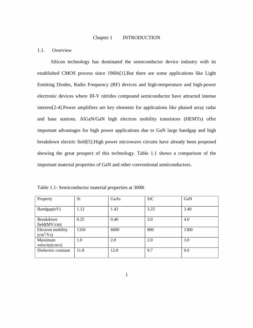
properties[26].Figure 1.4 shows the crystal structure of wurtzite Ga-face and N-face GaN.
Figure 1.4 Crystal structure of wurtzite Ga-face and N-face Gallium Nitride[26].
The HEMT structures are generally grown along the c-axes and the spontaneous
polarization along the axes is given by,
P = P zsp sp (1.1)
The piezoelectric polarization charge is evaluated by,
P = e ε + e (ε + ε )z x yPE 33 31 (1.2)
where, e33 and e31 are piezoelectric coefficients.Here,
8
c - c0ε =z c0 (1.3)
where, �� is the strain along the c axis and the strain in the plane perpendicular to the c-
axis is:
a - a0ε = ε =x y a0 (1.4)
The amount of piezoelectric polarization in the direction of the c axis can, thus, be
determined by
a - a C0 13P = 2 e - ePE 31 33a C0 33
(1.5)
where C13 and C33 are elastic constants. The piezoelectric polarization of AlGaN comes
out to be negative for tensile and positive for compressive strained barriers, respectively.
The spontaneous polarization for both GaN as well as AlN are found to be negative and
hence, for Ga(Al)-face heterostructures the spontaneous polarization will point towards
the substrate. The alignment of the piezoelectric and spontaneous polarization is parallel
in the case of tensile strain, and anti-parallel in the case of compressively strained top
layers as shown in Figure 1.5. If the polarity changes from Ga-face to N-face material,
the piezoelectric and spontaneous polarization changes its sign (Figure 1.5).

9
Figure 1.5 –Spontaneous and Piezoelectric polarization charge and their direction in Ga-
faced and N-faced strained and relaxed AlGaN/GaN HEMT [26].
The effective polarization charge at any interface is given by,
ρ =P P∇ (1.6)
where, ��is the polarization induced charge density.

10
σ = P(Top) - P(Bottom) (1.7)
σ = [P (Top) + P (Top)] - [P (Bottom) + P (Bottom)]PE PESP SP (1.8)
where, σ is the polarization sheet charge density.
The polarization induced sheet charge density is positive in pseudomorphically grown
AlGaN/GaN heterostructures and free electrons will tend to compensate the polarization
induced charge, thereby forming a two dimensional electron gas (2DEG) at the
AlGaN/GaN interface. A negative sheet charge density will accumulate holes at the
interface. The following set of linear interpolations between the physical properties of
GaN and AlN are utilized to calculate the net polarization induced sheet charge density
σ at the AlGaN/GaN as a function of the Aluminum mole fraction x of the AlxGa1-xN
barrier[26].
Lattice constant:
-10a(x) = (-0.077x + 3.189)10 m (1.9)
Elastic constants:
c (x) = (5x +103)GPa13 (1.10)
c (x) = (-32x + 405)GPa33 (1.11)
Piezoelectric constants:
2e (x) = (-0.11x - 0.49)C / m31 (1.12)

11
2e (x) = (0.73x + 0.73)C / m33 (1.13)
Spontaneous polarization:
2P (x) = (-0.052x - 0.029)C / mSP (1.14)
The GaN substrate is thick and therefore is not strained. Thus, its piezoelectric
component of polarization charge is taken as 0 C/m2.Therefore, the effective polarization
charge at the AlGaN/GaN interface is given by,
σ(x) = P (Al Ga N) + P (Al Ga N) - P (GaN)x xPE 1-x SP 1-x SP (1.15)
since,
σ = P(Top) - P(Bottom) (1.16)
The absence of stress along the growth direction helps us to represent the strain in
the z direction as,
c e AlGaN13 33ε = -2 ε + Ez x zc c33 33
(1.17)
where, AlGaNEz is the electric field in the AlGaN layer.
1.4. Thermal Issues of AlGaN/GaN HEMTs
Although the GaN based devices have the advantage of high electron density and
output current, the high current flow generates a lot of heat which is known as self-
heating. Self-heating is a serious concern in GaN devices. Due to self-heating, channel
temperatures can reach several hundred degrees above the ambient base temperature. The

12
temperature increases can significantly change the temperature dependent material
properties like band-gap and mobility which lead to degradation of device performance.
The reduction in mobility leads to a reduction in current due to increased operating
voltage. This decreases the maximum power density and also increases the gate leakage.
Figure 1.6 shows the dependence of mobility on sheet carrier concentration. Mobility
values at all temperatures reduce to same value for very high sheet concentration (>1020
cm-3). For small sheet carrier concentration the lower the temperature the higher the
carrier mobility[27].The dependence of the carrier mobility upon the temperature for
three different sheet carrier concentrations ns is shown in Figure 1.7.
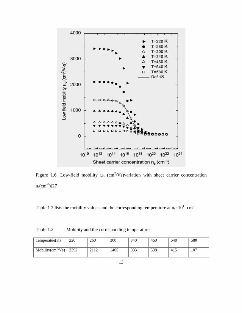
Figure 1.6. Low-field mobility µ
ns(cm-3)[27]
Table 1.2 lists the mobility values and the corresponding
Table 1.2 Mobility and the corresponding temperature
Temperatue(K) 220 260
Mobility(cm2/Vs) 3392 2112
13
field mobility µo (cm2/Vs)variation with sheet carrier concentration
lists the mobility values and the corresponding temperature at ns=10
Mobility and the corresponding temperature
260 300 340 460 540
2112 1405 983 538 415
/Vs)variation with sheet carrier concentration
=1011 cm-3.
580
107

Figure1.7. Dependence of low
The amount of self-heating also depends upon the thermal conductivity
that is used. Popular substrate materials currently used for GaN HEMTs include sapphire,
Silicon Carbide (SiC), silicon (Si)
14
Dependence of low-field mobility µo (cm2/Vs) on temperature T(K)
heating also depends upon the thermal conductivity of the substrate
Popular substrate materials currently used for GaN HEMTs include sapphire,
Silicon Carbide (SiC), silicon (Si) and Aluminum Nitride (AlN).Each substrate choice
on temperature T(K)[27].
of the substrate
Popular substrate materials currently used for GaN HEMTs include sapphire,
Each substrate choice

15
has been proven with individual successes.
• Sapphire(Al2O3) had been a popular choice for substrate material due to its
high melting point and ready availability. GaN purity levels are affected
during vapor growth by the interaction of hydrogen gas and the oxygen in
sapphire, creating unwanted defects, thus limiting the mobility. The thermal
conductivity of sapphire has also been a limiting factor[28].
• Pure silicon has been used quite successfully as a substrate material for GaN
HEMTs. Thermal conductivity of Si is similar to that of GaN. High purity
silicon is readily available. However, lattice mismatch requires the use of a
nucleation layer, further increasing the channel distance from the thermal
management substrate [29].
• SiC has been a popular choice for high-power HEMT use providing a much
higher thermal conductivity. But defects in SiC have made GaN layer growth
difficult as the structure struggles to maintain uniformity during the crystal
growth process [28]. AlN is often used as a nucleation layer between silicon
based substrates and GaN to allow for lattice matching.
• As a free standing substrate, AlN has shown some promise as a GaN HEMT
substrate choice but its thermal conductivity is only equal to that of sapphire.
• Bulk GaN substrate can eliminate trapping defect. But the thermal
conductivity of GaN is a challenge to overcome which can lead to loss of
linearity and device breakdown. While able to support high temperature
operation, GaN by itself is unable to sufficiently remove the heat generated
during device operation.
• Diamond, which has the best thermal conductivity, is an option for GaN
HEMT devices.
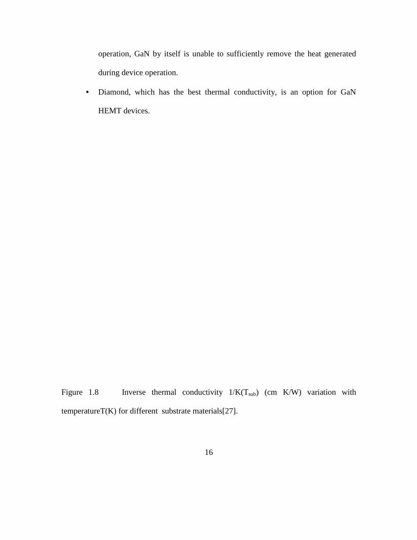
Figure 1.8 Inverse thermal conductivity 1/K(T
temperatureT(K) for different
16
operation, GaN by itself is unable to sufficiently remove the heat generated
during device operation.
Diamond, which has the best thermal conductivity, is an option for GaN
Inverse thermal conductivity 1/K(Tsub) (cm K/W) variation with
T(K) for different substrate materials[27].
operation, GaN by itself is unable to sufficiently remove the heat generated
Diamond, which has the best thermal conductivity, is an option for GaN
variation with
17
The GaN HEMT with best power performance till now has been grown on SiC. Figure
1.8 presents the temperature dependence of inverse of the thermal conductivity(1/K) of
various materials that can be used as substrates in AlGaN/GaN HEMTs. If the total
epilayer thickness in the devices is significantly smaller than the device length, the
thermal conductivity of the substrate plays a significant role in determining the
temperature distribution profile in the epilayer structure and the heat dissipation from the
active region of the device [27].
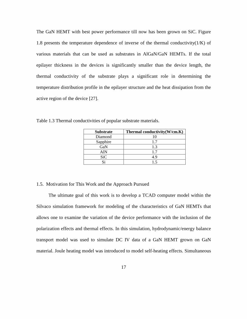
Table 1.3 Thermal conductivities of popular substrate materials.
Substrate Thermal conductivity(W/cm.K) Diamond 10 Sapphire 1.7
GaN 1.3 AlN 1.7 SiC 4.9 Si 1.5
1.5. Motivation for This Work and the Approach Pursued
The ultimate goal of this work is to develop a TCAD computer model within the
Silvaco simulation framework for modeling of the characteristics of GaN HEMTs that
allows one to examine the variation of the device performance with the inclusion of the
polarization effects and thermal effects. In this simulation, hydrodynamic/energy balance
transport model was used to simulate DC IV data of a GaN HEMT grown on GaN
material. Joule heating model was introduced to model self-heating effects. Simultaneous

18
understanding the thermal and electrical properties of the GaN HEMTs allows for better
optimization of the GaN transistor structure and prediction of thermal conductivity across
layer interfaces.
Chapter 2 discusses the modeling approach used in Silvaco for analyzing the operation of
GaN HEMTs. Chapters 3 presents important results for the different device simulations
(with and without the inclusion of some of the effects studied), and summarizes the
influence that these effects have on the device characteristics. Chapter 4 summarizes the
results of this work and also provides thoughts on the scope for future research work.

19
Chapter 2 DEVICE MODELING AND SIMULATION
2.1. Semiconductor Device Simulations
Semiconductor device simulations provide in depth understanding of actual
operations of solid state devices while at the same time reducing the computational
burden so that the results can be obtained within a reasonable time frame.
2.1.1. Importance of Simulation
The semiconductor Industry has developed device simulations tools to reduce
costs for R&D and production facilities. Semiconductor device modeling creates models
for the behavior of the electrical devices based on fundamental physics. It may also
include the creation of compact models which represent the electrical behavior of such
devices but do not derive them from underlying physics. Device modeling offers many
advantages such as: providing in-depth understanding, providing problem diagnostics and
decreasing design cycle time. Simulations require enormous technical expertise not only
in simulation techniques and tools but also in the fields of physics and chemistry. The
developer of simulation tools needs to be closely related to the development activities in
the research and commercial productions in industry.
2.1.2. General Device Simulation Framework
Figure 2.1 shows the main components of semiconductor device simulations at
any level. It all begins with the electronic properties of solid state materials. The two
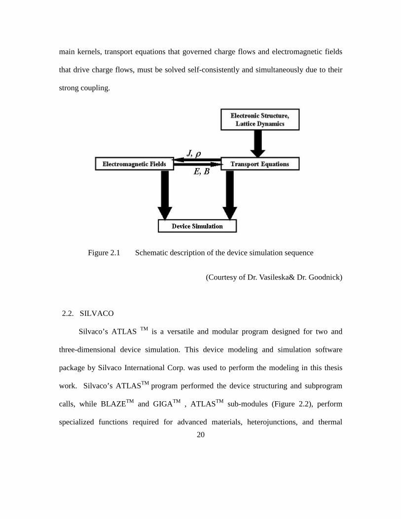
20
main kernels, transport equations that governed charge flows and electromagnetic fields
that drive charge flows, must be solved self-consistently and simultaneously due to their
strong coupling.
Figure 2.1 Schematic description of the device simulation sequence
(Courtesy of Dr. Vasileska& Dr. Goodnick)
2.2. SILVACO
Silvaco’s ATLAS TM is a versatile and modular program designed for two and
three-dimensional device simulation. This device modeling and simulation software
package by Silvaco International Corp. was used to perform the modeling in this thesis
work. Silvaco’s ATLASTM program performed the device structuring and subprogram
calls, while BLAZETM and GIGATM , ATLASTM sub-modules (Figure 2.2), perform
specialized functions required for advanced materials, heterojunctions, and thermal

21
modeling. To control, modify, and display the modeling and simulation, the Virtual
Wafer Fabrication (VWF) Interactive Tools, namely DECKBUILDTM and
TONYPLOTTM were utilized (see Figure 2.3 below).
Figure 2.2 Representation of ATLAS’ modular structure[30].
22
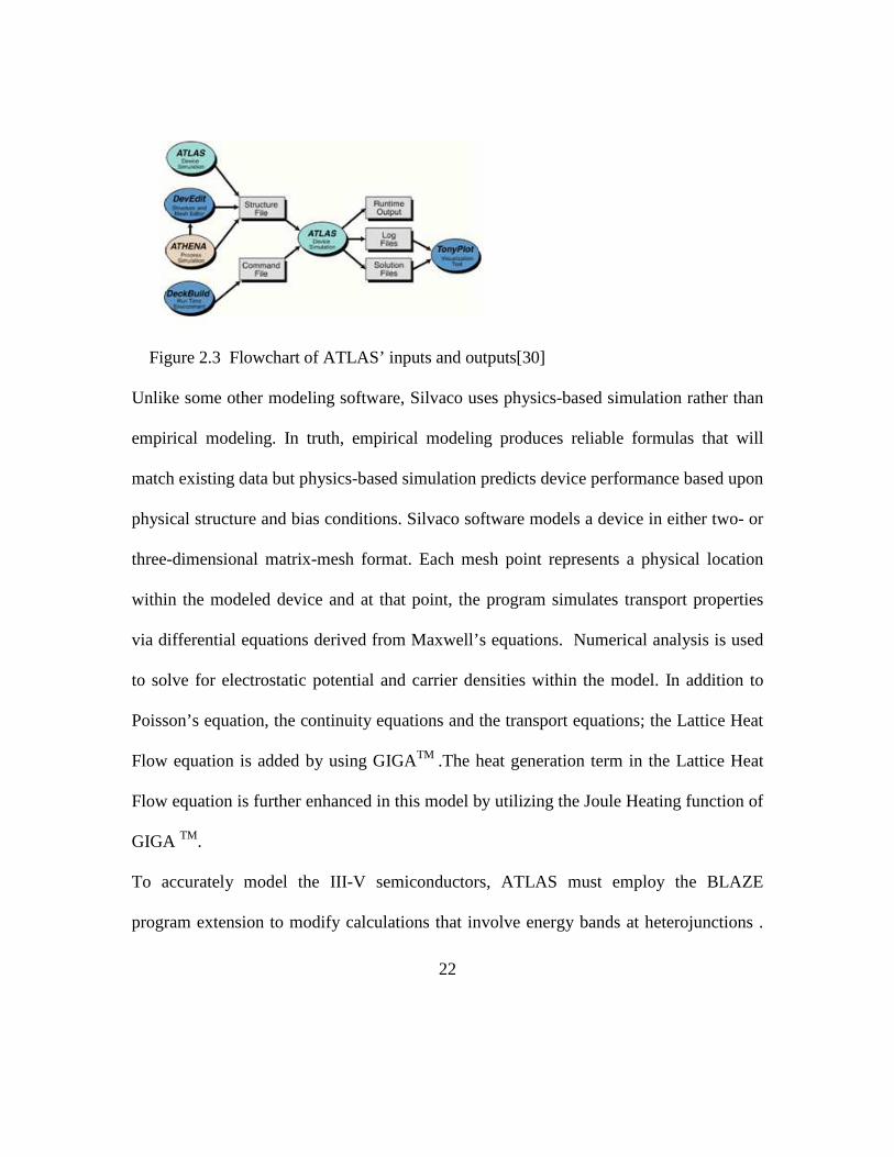
Figure 2.3 Flowchart of ATLAS’ inputs and outputs[30]
Unlike some other modeling software, Silvaco uses physics-based simulation rather than
empirical modeling. In truth, empirical modeling produces reliable formulas that will
match existing data but physics-based simulation predicts device performance based upon
physical structure and bias conditions. Silvaco software models a device in either two- or
three-dimensional matrix-mesh format. Each mesh point represents a physical location
within the modeled device and at that point, the program simulates transport properties
via differential equations derived from Maxwell’s equations. Numerical analysis is used
to solve for electrostatic potential and carrier densities within the model. In addition to
Poisson’s equation, the continuity equations and the transport equations; the Lattice Heat
Flow equation is added by using GIGATM .The heat generation term in the Lattice Heat
Flow equation is further enhanced in this model by utilizing the Joule Heating function of
GIGA TM.
To accurately model the III-V semiconductors, ATLAS must employ the BLAZE
program extension to modify calculations that involve energy bands at heterojunctions .

23
The heterojunctions require changes in calculating current densities, thermionic
emissions, velocity saturation, and recombination-generation.
ATLAS attempts to find solutions to carrier parameters such as current through
electrodes, carrier concentrations, and electric fields throughout the device. ATLAS sets
up the equations with an initial guess for parameter values then iterates through
parameters to resolve discrepancies. ATLAS will alternatively use a decoupled (Gummel)
approach or a coupled (Newton) approach to achieve an acceptable correspondence of
values. When convergence on acceptable values does not occur, the program
automatically reduces the iteration step size. ATLAS generates the initial guess for
parameter values by solving a zero-bias condition based on doping profiles in the device.
2.3. Device Structures Being Simulated
This work focuses on two GaN HEMT structures. One is an Al0.25Ga0.75N/GaN
HEMT. A GaN/AlGaN/AlN/GaN device is also being simulated. Inserting a very thin
AlN interfacial layer between the AlGaN and GaN layers helps to increase the sheet
charge density and improves mobility of the carriers in the channel. This owes to the
reduction of alloy disorder scattering in AlGaN/AlN/GaN HEMT’s when compared to
AlGaN/GaN HEMT’s. Since, the barrier height (conduction band difference) of
AlN/GaN layer is larger than AlGaN/GaN layer, the probability of the channel electrons
entering the AlGaN layer reduces significantly. This helps in reducing the impact of alloy

24
disorder scattering on the electron mobility, arising from the defects in the AlGaN
layer[31-34].
2.3.1. AlGaN/GaN HEMT
Figure 2.4 Simulated 2D AlGaN/GaN HEMT Structure.
Figure 2.4 shows the simulated AlGaN/GaN HEMT structure. A 23nm unintentionally
doped AlGaN layer was formed on 100nm of the unintentionally doped GaN layer. An
unintentionally doping of 1017 cm-3 is assumed for both the AlGaN and GaN layers. The
source and drain electrodes are Ohmic contacts and are doped to 1018 cm-3. The gate
electrode is a Schottky contact, and the Schottky barrier height is calculated to be equal to
1.17eV[35].Figure 2.5 is the ATLAS-generated representation of the
Al 0.25Ga0.75N/GaNHEMT device.
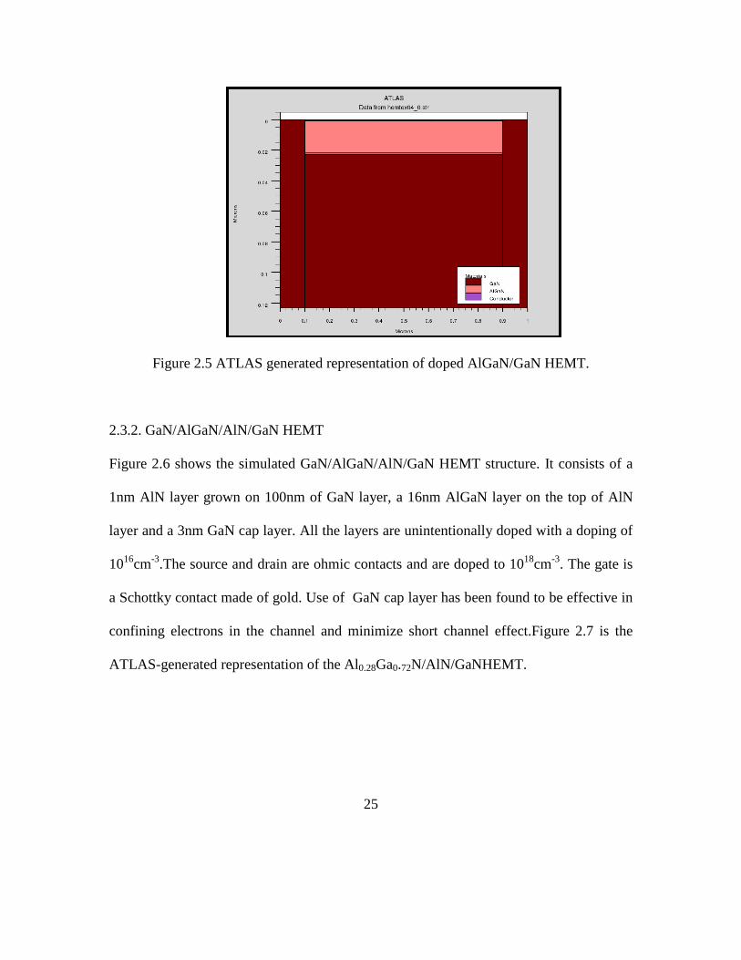
25
Figure 2.5 ATLAS generated representation of doped AlGaN/GaN HEMT.
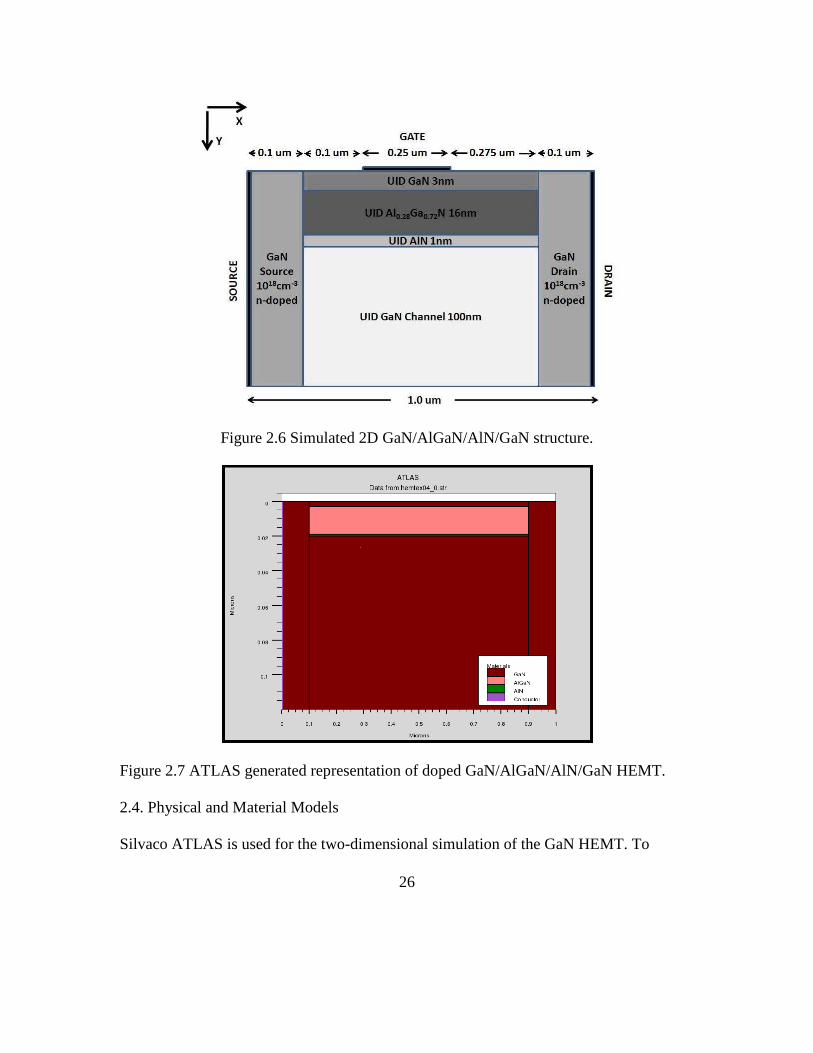
2.3.2. GaN/AlGaN/AlN/GaN HEMT
Figure 2.6 shows the simulated GaN/AlGaN/AlN/GaN HEMT structure. It consists of a
1nm AlN layer grown on 100nm of GaN layer, a 16nm AlGaN layer on the top of AlN
layer and a 3nm GaN cap layer. All the layers are unintentionally doped with a doping of
1016cm-3.The source and drain are ohmic contacts and are doped to 1018cm-3. The gate is
a Schottky contact made of gold. Use of GaN cap layer has been found to be effective in
confining electrons in the channel and minimize short channel effect.Figure 2.7 is the
ATLAS-generated representation of the Al0.28Ga0.72N/AlN/GaNHEMT.
26
Figure 2.6 Simulated 2D GaN/AlGaN/AlN/GaN structure.
Figure 2.7 ATLAS generated representation of doped GaN/AlGaN/AlN/GaN HEMT.
2.4. Physical and Material Models
Silvaco ATLAS is used for the two-dimensional simulation of the GaN HEMT. To

27
accurately model the III-V semiconductors, ATLAS must employ the BLAZE program
extension to modify calculations that involve energy bands at the heterostructure.
The heterojunctions require change in calculating current densities, velocity saturation
and recombination-generation. The hydrodynamic/Energy Balance carrier transport
model is used to achieve maximum accuracy as well as computational efficiency. This
model takes account of non-local carrier heating effects for device structures with gate
length less than 0.5 microns. As AlGaN/GaN HEMTs are unipolar devices,
computational effort is reduced by neglecting the transport equations for holes in this
work.
When using TCAD simulation software, a number of physical models have to be
included into the model to perform simulations and do reliable predictions about device
characteristics so that they closely match real device data. These models deal with the
carrier behavior in combined effects of boundary conditions such as lattice temperature,
electrostatic potential and fields, external forces and hetero-structures bandgap variations.
Because of the high operating voltages, self-heating effects need to be accounted for in
the model construction.
2.4.1. Drift-Diffusion(DD) Transport Model(Homogenous Structure)
Drift-diffusion is a transport model which approximates that the carrier flow
inside the device is due to the drift and diffusion under an external lateral or longitudinal

28
field concurrently with recombination and generation processes. The current density is
given by [36]:
n n nJ nqµ φ= − ∇ (2.1)
p p pJ pqµ φ= − ∇ (2.2)
Where nµ and pµare electron and hole mobility respectively ,nφ and pφ
are the respective
quasi Fermi levels ,p is the hole density and n is electron density. The quasi Fermi levels
are linked to the carrier concentrations and the potential through the Boltzmann
approximation:
( )exp n
ieL
qn n
kT
ψ ϕ −=
(2.3)
( )exp p
ieL
qp n
kT
ψ ϕ− =
(2.4)
Where ien is the effective intrinsic concentration and TL is the lattice temperature ,k is the
Boltzmann’s constant, kTL is the thermal energy in the system. These two equations may
be rewritten to give the quasi-Fermi levels:
lnLn
ie
kT n
q nϕ = Ψ − (2.5)
lnLp
ie
kT p
q nϕ = Ψ −
(2.6)
By substituting these equations into the current density equations, the following equations
are obtained:

29
( (ln ))n n n n L ieJ qD n qn n kT nµ ψ µ= ∇ − ∇ − ∇���
(2.7)
( (ln ))p p p p L ieJ qD p qp p kT nµ ψ µ= ∇ − ∇ − ∇���
(2.8)
The final term accounts for the gradient in the effective intrinsic carrier concentration,
which takes account of the bandgap narrowing effects. Effective electric fields are
defined normally as:
( ln )Ln ie
kTE n
qψ= −∇ +
���
(2.9)
( ln )Lp ie
kTE n
qψ= −∇ +
���
(2.10)
Which then allows the more conventional formulation of drift-diffusion equations to be
written:
n n n nJ qn E qD nµ= + ∇��� ���
(2.11)
p p p pJ qp E qD pµ= − ∇��� ���
(2.12)
This derivation has assumed that Einstein relationship holds. In case of Boltzmann
statistics this corresponds to:
Ln n
kTD
qµ=
(2.13)
Lp p
kTD
qµ= (2.14)
If Fermi-Dirac statistics are assumed for electrons then equation(2.13) becomes:

30
12
12
1( ) [ ]
1[ ]
Ln Fn C
Ln
Fn CL
kTF
q kTD
FkT
µ ε ε
ε ε−
−
=
− (2.15)
Where Fα is Fermi-Dirac integral of order α and Fnε is given by - nqφ .
2.4.2. Drift-diffusion with Position Dependent Band Structure(Heterostructure)
The current density equations must be modified to take into account the non-
uniform band structure[37].The current density equations are [38]:
n n nJ nµ φ= − ∇���
(2.16)
p p pJ nµ φ= − ∇���
(2.17)
Where nµ and pµ are electron and hole mobility respectively, nφ and pφ are the respective
quasi Fermi levels.
1n FNE
qφ = (2.18)
1p FPE
qφ =
(2.19)
The conduction and valence band edge energies can be written as:
0( )CE q ψ ψ χ= − − (2.20)
0( )V gE q Eψ ψ χ= − − − (2.21)

31
Where 0ψ is some reference potential, χ is position dependent electron affinity, gE is
position dependent bandgap and
0 ln lnr gcr vrr L L
ir ir
EN NkT kT
q q n q q n
χχψ+
= + = − (2.22)
wherenir is the intrinsic carrier concentration of the selected reference material, and r is
the index that indicates that all of the parameters are taken from reference material. Fermi
energies are expressed in the form:
lnFN C L Lc
nE E kT ln kT n
Nγ= + − (2.23)
lnFP V L Lv
nE E kT ln kT n
Nγ= + − (2.24)
The last terms on the RHS in equations (2.23) and(2.24)are due to the influence of
Fermi-Dirac statistics. These final terms are defined as follows:
( )12
n
n
n
F
eη
ηγ = , 1
12
FN Cn
L c
E E nF
kT Nη − −
= =
(2.25)
( )12
p
p
p
F
eη
ηγ = , 1
12
v Fpp
L p
E E pF
kT Nη −
−= =
(2.26)
Where Nc and Nv are position dependent and 1n pγ γ= = for Boltzmann statistics. By
combining the above results, one can obtain the following expression for the current
densities:

32
ln ln CL Ln L n n n
ir
NkT kTJ kT n q n
q q q n
χµ µ ψ γ
= ∇ − ∇ + + +
���
(2.27)
ln lng VL Lp L p p p
ir
E NkT kTJ kT p q p
q q q n
χµ µ ψ γ
+ = ∇ − ∇ + + +
���
(2.28)
2.4.3. Hydrodynamic/Energy Balance Transport Model
The conventional drift-diffusion model of charge transport neglects non–local
transport effects such as velocity overshoot, diffusion associated with the carrier
temperature and the dependence of impact ionization rates on carrier energy distributions.
These phenomena can have a significant effect in case of submicron devices. As a result
ATLAS offers two non-local models of charge transport, the energy balance and the
hydrodynamic models. The Energy Balance Transport Model follows the derivation by
Stratton [39,40]. Hydrodynamic model is derived from this model by applying certain
assumptions[41,42,43].
The Energy Balance Transport Model adds continuity equations for the carrier
temperatures, and treats mobilities and impact ionization coefficients as functions of the
carrier temperatures(Tn,Tp) rather than functions of the local electric field. For electrons,
the Energy Balance Transport Model consists of:
*1 3iv . ( )
2n n n n n
kd S J E W nT
q tλ∂= − −
∂
��� ��� ��
(2.29)
Tn n n n nJ qD n qn qnD Tµ ψ= ∇ − ∇ + ∇���
(2.30)

33
nn n n n n
kS K T J T
q
δ = − ∇ −
��� ���
(2.31)
( )3 3( )
2 . 2n L A
n n n n SRH g n n
k T TW n kT R E G R
TAUREL ELλ λ
−= + + − (2.32)
3 1
2 2
( ) / ( )n n nF h F hλ = (2.33)
And for holes:
*1 3iv . ( )
2p p p p p
kd S J E W nT
q tλ∂= − −
∂
��� ��� ��
(2.34)
Tp p p p pJ qD p qp qpD Tµ ψ= − ∇ − ∇ + ∇���
(2.35)
pp p p p p
kS K T J T
q
δ = − ∇ −
��� ���
(2.36)
( )3 3( )
2 . 2
p L Ap p p p SRH g p p
k T TW p kT R E G R
TAUREL HOλ λ
−= + + −
(2.37)
3 1
2 2
( ) / ( )p p pF h F hλ = (2.38)
Where nS���
and pS���
are energy flux densities associated with electrons and holes, and nµ
and pµare the electron and hole mobilities, RSRH is the SRH recombination rate, Rn
A and
RpAare Auger recombination rates related to electron and holes, Gn and Gp are impact
ionization rates, TAUREL.EL and TAUREL.HO are the electron and hole energy
relaxation times, Eg is the banggap energy of the semiconductor. The relaxation
parameters are user-definable on the MATERIAL statement. The relaxation times are

34
extremely important as they define the time constant for the rate of energy exchange and
therefore accurate values are required if the model is to be accurate.
The remaining terms, Dn and Dp are the thermal diffusivities for electrons and holes. Wn
and Wp are the energy density loss rates for electrons and holes as defined in (2.32) and
(2.37) respectively. Thus, the following relationships hold:
*n nn n
kTD
q
µ λ= (2.39)
*1( )( )21( )( )2
n
n
n
F
F
ηλ
η=
− (2.40)
where 11 2 ( )nF C
nn C
nF
kT N
ε εη −−
= = (2.41)
*2
3( )
2T
n n n n
kD
qµ λ µ= − (2.42)
2
3 ( )5 2( )12 ( )2
n n
n n n
n n
F
F
ξ
ξ
ηµ µ ξ
η
+= +
+ (2.43)
2. ( )n n n
kKn q n T
qµ= ∆
(2.44)
5 3( ) ( )7 52 23 12 2 ( )( ) 22
n n n n
n n n n
n nn n
F F
FF
ξ ξ
ξξ
η ηδ ξ ξ
ηη
+ + ∆ = + − + ++ (2.45)
2nn
n
µδµ
= (2.46)

35
Similar expressions for holes are as follows:
*p pp p
kTD
q
µλ=
(2.47)
*1( )( )21( )( )2
p
p
p
F
F
ηλ
η=
− (2.48)
where
11 2 ( )pV f
pp V
pF
kT N
ε εη −
−= =
(2.49)
*2
3( )
2T
p p p p
kD
qµ λ µ= − (2.50)
2
3 ( )5 2( )12 ( )2
p p
p p p
p p
F
F
ξ
ξ
ηµ µ ξ
η
+= +
+ (2.51)
2. ( )p p p
kKp q p T
qµ= ∆ (2.52)
5 3( ) ( )7 52 23 12 2 ( )( ) 22
p p p p
p p p p
p pp p
F F
FF
ξ ξ
ξξ
η ηδ ξ ξ
ηη
+ + ∆ = + − + ++
(2.53)
2 pp
p
µδ
µ=
(2.54)
Kn and Kp are thermal conductivities of electrons and holes as defined in (2.44) and (2.52)
respectively. If Boltzmann statistics are used in preference to Fermi statistics, the above
equations simplify to :
* * 1n pλ λ= = (2.55)

36
5
2n n nδ ξ ∆ = = +
(2.56)
5
2p p pδ ξ ∆ = = +
(2.57)
(ln )
(ln )n n n
nn n n
d T
d T T
µ µξµ
∂= =
∂ (2.58)
(ln )
(ln )p P P
pp P P
d T
d T T
µ µξµ
∂= =
∂ (2.59)
The parameters nξ and pξare carrier temperature dependent. Different assumptions
regarding nξ and pξcorrespond to different non-local models. In the high-field saturated
velocity model , the carrier mobilities are inversely proportional to carrier temperature.
Thus:
1n pξ ξ= = − (2.60)
corresponds to Energy Balance Transport Model. Furthermore when
0n pξ ξ= = , (2.61)
this corresponds to the simplified Hydrodynamic Transport Model.
The parameters nξ and pξcan be specified using the KSN and KSP parameters in the
MODELS statement.
Hot carrier transport equations are activated by the MODELS statement parameter:
HCTE.EL (electron temperature),HCTE.HL(hole temperature),HCTE(both carrier
temperature)[38].

37
2.4.4. Hydrodynamic Boundary conditions
Boundary conditions for n,p and ψ are same as for drift-diffusion model. Energy
balance equations are solved only in the semiconductor region. Electron and hole
temperatures are set equal to lattice temperature on the contacts. On the other part of the
boundary , the normal components of the energy fluxes vanish.
2.4.5. Boundary Physics: Ohmic and Schottky Contact
Many of useful properties of p-n junctions can be achieved by forming different
metal-semiconductor contacts[44].The major difference between ohmic and Schottky
contact is the Schottky barrier height, φB, is non-positive or positive. For ohmic contacts,
the barrier height should be near zero or negative, formed accumulation type contact, thus
the majority carriers are free to flow out the semiconductors, as shown below in Figure
2.8. On the contrary, for Schottky contacts, the barrier height would be positive, built
depletion type contacts, so that the majority carriers cannot be absorbed freely due to the
band bending caused by positive barrier height. Hence the way they are implemented in
the simulator is different.

38
Figure 2.8 Accumulation type ohmic contact.
2.4.5.1. Ohmic Contacts
Ohmic contacts are implemented as simple Dirichlet’s boundary condition, where
surface potential, hole concentration and electron concentration are fixed( ), ,s s sn pΨ .
Minority and majority carrier quasi-Fermi potentials are equal to the applied bias of the
electrode( )n p appliedVφ φ= = . The potential sψ is fixed at a value that is consistent with
space charge neutrality. If Boltzmann statistics is used then
ln lns sL Ls n p
ie ie
n pkT kT
q n q nψ φ φ= + = − (2.62)
where nie is intrinsic carrier concentration[38].
If work function is not specified, the contact will be ohmic regardless of the material.
2.4.5.2. Schottky Contacts
The surface potential of the Schottky contact is given by:

39
ln2 2
g CLs applied
V
E NkTAFFINITY WORKFUN V
q q Nψ = + + − + (2.63)
where AFFINITY is the electron affinity of the semiconductor material, Eg is the
bandgap,Nc is the conduction band density of states, Nv is the valence band density of
states, and TL is the ambient temperature. The workfunction is defined as:
WORKFUN=AFFINITY+ Bφ (2.64)
Where Bφ is the barrier height at the metal-semiconductor interface in eV[38].A
Schottky contact[45]is implemented by specifying workfunction using the WORKFUN
in the parameter of the contact statement.
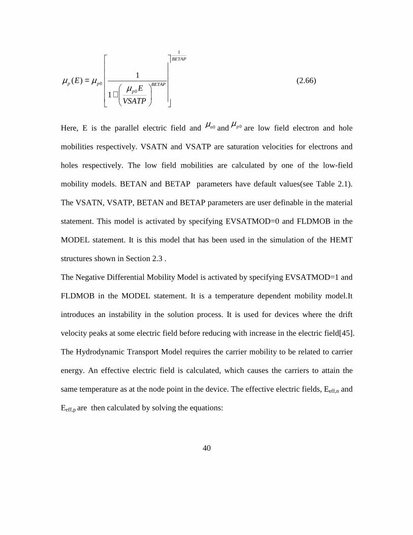
2.4.6. Mobility Model
There are two types of electric field dependent mobility models used in
ATLAS/BLAZE. These models are Standard Mobility Model and Negative Differential
Mobility Model. The standard mobility model takes account of velocity saturation. The
following Caughey and Thomas expression[46] is used to implement a field-dependent
mobility:
1
0
0
1( )
1
BETAN
n n BETAN
n
EE
VSATN
µ µµ
= +
(2.65)
40
1
0
0
1( )
1
BETAP
p p BETAP
p
EE
VSATP
µ µµ
=
+
(2.66)
Here, E is the parallel electric field and 0nµ and 0pµare low field electron and hole
mobilities respectively. VSATN and VSATP are saturation velocities for electrons and
holes respectively. The low field mobilities are calculated by one of the low-field
mobility models. BETAN and BETAP parameters have default values(see Table 2.1).
The VSATN, VSATP, BETAN and BETAP parameters are user definable in the material
statement. This model is activated by specifying EVSATMOD=0 and FLDMOB in the
MODEL statement. It is this model that has been used in the simulation of the HEMT
structures shown in Section 2.3 .
The Negative Differential Mobility Model is activated by specifying EVSATMOD=1 and
FLDMOB in the MODEL statement. It is a temperature dependent mobility model.It
introduces an instability in the solution process. It is used for devices where the drift
velocity peaks at some electric field before reducing with increase in the electric field[45].
The Hydrodynamic Transport Model requires the carrier mobility to be related to carrier
energy. An effective electric field is calculated, which causes the carriers to attain the
same temperature as at the node point in the device. The effective electric fields, Eeff,n and
Eeff,p are then calculated by solving the equations:

41
( ) 2, ,
( )3
2 .n L
n eff n eff n
k T Tq E E
TAUMOB ELµ −
= (2.67)
( ) 2, ,
( )3
2 .p L
P eff n eff p
k T Tq E E
TAUMOB HOµ
−=
(2.68)
These equations are derived from energy balance equations by stripping out all the
spatially varying terms. The effective electric fields are then introduced into the relevant
field dependent mobility model.
The resultant relationship between carrier mobility and carrier temperature is
given by:
( )0
1
1
nn
BETAN BETANnX
µµ =+
(2.69)
( )0
1
1
PP
BETAP BETAPPX
µµ =+
(2.70)
( )2 21( ) ( ) 4 ( )
2BETAN BETAN BETAN BETAN BETAN BETAN BETAN
n n n L n n L n n LX T T T T T Tα α α= − + − − − (2.71)
( )2 21( ) ( ) 4 ( )
2BETAN BETAP BETAP BETAP BETAP BETAP BETAP
P P P L P P L P P LX T T T T T Tα α α= − + − − − (2.72)
( )0
2
3
2 .B n
n
k
qVSATN TAUREL EL
µα = (2.73)
( )0
2
3
2 .B p
p
k
qVSATP TAUREL HO
µα = (2.74)

42
As carriers are accelerated in an electric field, their velocity will begin to saturate when
the electric field magnitude becomes significant. This effect has to be accounted for by a
reduction of effective mobility since the magnitude of drift velocity is the product of
mobility and the electric field component in the direction of the current flow. This
provides a smooth transition between low-field and high field behavior.
The saturation velocities are calculated by default from the temperature dependent
model[47]:
.
1 . exp.
L
ALPHAN FLDVSATN
TTHETAN FLD
TNOMN FLD
= +
(2.75)
.
1 . exp.
L
ALPHAP FLDVSATP
TTHETAP FLD
TNOMP FLD
= +
(2.76)
One can set them to constant values on the MOBILITY statement using VSATN and
VSATP parameters.

43
Table 2.1 User definable parameters in field-dependent mobility model.
Statement Parameter Default Units
MOBILITY ALPHAN.FLD 2.4X107 cm/s
MOBILITY ALPHAP.FLD 2.4X107 cm/s
MOBILITY BETAN 2.0
MOBILITY BETAP 1.0
MOBILITY THETAN.FLD 0.8
MOBILITY THETAP.FLD 0.8
MOBILITY TNOMN.FLD 600.0 K
MOBILITY TNOMP.FLD 600.0 K
2.4.7 Spontaneous and Piezoelectric Polarization Implementation
A good understanding of the electrical polarization effects at the AlxGa1-xN/GaN
interface is a key to proper device simulation. The spontaneous polarization Psp and the
strain induced piezoelectric polarization Pz are calculated by using:
( )P P P 1 xsp GaNAl Ga N 1 xsp sp
x= + −
− (2.77)
0 1331 33
0 33
2 sz
a a cP e e
a c
−= −
(2.78)

44
where a0 and as are lattice constants and 31e and 33e are piezoelectric coefficients and c13,
c33 are elastic constants[36].In this simulation, this interface charge was implemented by
making the region near the heterojunction highly doped n-type at the interface.
2.5. Self-heating Simulations
This section briefly describes the models used to simulate self-heating effects with
TCAD. These models are described in more details in the simulator manual[38]. Briefly,
the non-isothermal model modifies the drift-diffusion equations to account for the self-
heating effects. The assumption here is that the lattice is in thermal equilibrium with the
charge carriers. This implies that carrier and lattice temperature are described by a single
quantity TL. TL is calculated by coupling the lattice heat equation and the modified drift-
diffusion equation.
2.5.1. Overview
GIGA module extends the Silvaco TCAD software to account for lattice heat
flow and general thermal environments. GIGA implements Wachutka’s
thermodynamically rigorous model of lattice heating[48], which account for Joule
heating, heating and cooling due to carrier generation and recombination , and Peltier and
Thomson effects.
2.5.2 Numerics
45
GIGA module supplies numerical techniques that provide efficient solution of
equations that result when lattice heating is accounted for. These numerical techniques
include fully-coupled and block iteration method. When GIGA is used with energy
balance equations, the result is a solver for six PDEs.
2.5.3 Non-Isothermal Models
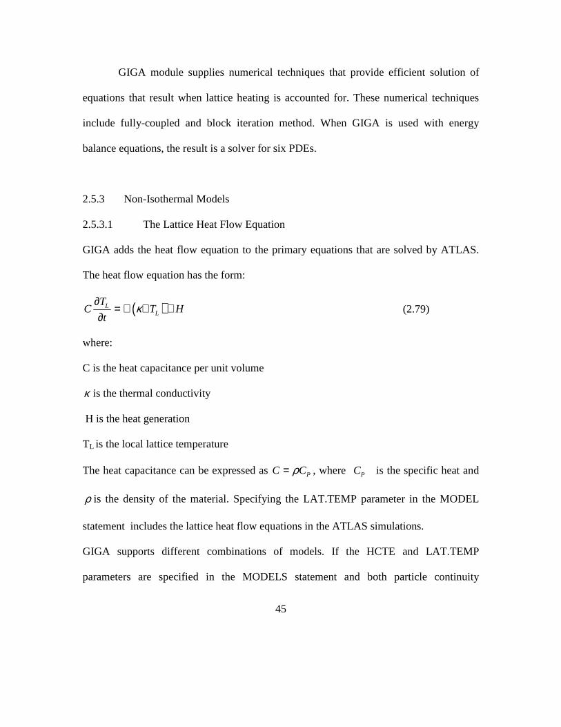
2.5.3.1 The Lattice Heat Flow Equation
GIGA adds the heat flow equation to the primary equations that are solved by ATLAS.
The heat flow equation has the form:
( )LL
TC T H
tκ∂
= ∇ ∇ +∂
(2.79)
where:
C is the heat capacitance per unit volume
κ is the thermal conductivity
H is the heat generation
TL is the local lattice temperature
The heat capacitance can be expressed as PC Cρ= , where PC is the specific heat and
ρ is the density of the material. Specifying the LAT.TEMP parameter in the MODEL
statement includes the lattice heat flow equations in the ATLAS simulations.
GIGA supports different combinations of models. If the HCTE and LAT.TEMP
parameters are specified in the MODELS statement and both particle continuity
46
equations are solved, all six equations are solved. If HCTE.EL is specified instead of
HCTE, only five equations are solved and hole temperature Tp is set equal to lattice
temperature TL.
2.5.3.2 Effective Density of States
When lattice heating is specified with energy balance model, the effective densities of
states are modeled as functions of the local carrier temperature , Tn and Tp, as defined by:
3 3* 2 2
2
2(300)
300e n n
C
m kT TN NC
h
π = =
(2.80)
3 3* 2 2
2
2(300)
300P p p
V
m kT TN NV
h
π = =
(2.81)
2.5.3.3 Non-Isothermal Current Densities
When GIGA is used, the electron and hole current densities are modified to account for
lattice temperatures:
( )n n n n LJ q n P Tµ φ= − ∇ + ∇���
(2.82)
( )p p p p LJ q p P Tµ φ= − ∇ + ∇���
(2.83)
Where Pn and Pp are absolute thermoelectric powers for electrons and holes. Pn and Pp are
expressed as follows:
47
Nk 5 CBP = - + ln + KSN +ξn nQ 2 n
(2.84)
Nk 5 VBP = + ln + KSP +ξp pQ 2 p
(2.85)
Here, kB is the Boltzmann constant. KSN and KSP are the exponents in the power law
relationship between relaxation time(mobility) and carrier energy. They are set on the
MODELS statement. The quantities nξ and Pξ are the phonon drag contribution to the
thermopower. ATLAS has a built in model for it and specifying PHONONDRAG
parameter on the MODELS statement enables it. The built-in model is:
PDEXP.Nk TB Lξ = PDA.Nn Q 300
for electrons (2.86)
PDEXP.Pk TB Lξ = PDA.Pp Q 300
for holes (2.87)
A theoretically derived value for PDEXP.N and PDEXP.N is 72− [49] but
experimentally obtained value is close to 52− [50].The values of PDA.N and PDA.P
depend on the doping level and sample size. So, one has to determine values to fit his
sample.
The thermopower consists of three components. The first is the derivative of the Fermi
Potential with respect to temperature. ATLAS incorporates this effect indirectly through
the boundary conditions. For Maxwell-Boltzmann statistics, this is

48
3ln
2CB Nk
Q n
− +
for electrons (2.88)
3ln
2VB Nk
Q p
+
for hole (2.89)
The second term is due to carrier scattering.
(1 )BkKSN
Q+ for electrons (2.90)
(1 )BkKSP
Q+ for holes (2.91)
The third term is the phonon drag contribution nξ− and pξ . The second and third terms
are included directly into the temperature gradient term in the expressions for current[38].
2.5.3.4. Heat generation
When carrier transport is handled in the drift-diffusion approximation the heat generation
term H has the form:
( ) ( )2 2
, ,
, ,
( )
n p
L n n L p pn p
pnL n L p
n p n p
pnL n n L p p
n p n p
J JH T J P T J P
q n q p
q R G T TT T
T P divJ T P divJT T
µ µ
φφ φ φ
φφ
= + − ∇ − ∇
∂ ∂ + − − − + ∂ ∂
∂ ∂ − + − + ∂ ∂
��� ���
��� ���
(2.92)
In the steady-state case current divergence can be replaced with the net recombination,
then the above equation simplifies to:

49
( ) ( )2 2
( )n p
p n L p n L n n p pn p
J JH q R G T P P T J P J P
q n q pφ φ
µ µ
= + + − − + − − ∇ + ∇
��� ���
��� ���
(2.93)
where:
2 2
n p
n p
J J
q n q pµ µ
+
��� ���
is the Joule heating term , ( )( ) p n L p nq R G T P Pφ φ − − + − is the
recombination and generation heating and cooling term, ( )L n n p pT J P J P− ∇ + ∇��� ���
accounts
for the Peltier and Joule-Thomson effects . A simple form of H that is widely used is:
( )n pH J J E= +��� ��� ��
(2.94)
GIGA can use either equation(2.93) or (2.94) for steady-state calculations. By default,
equation(2.94) is used. If HEAT.FULL in specified in the MODELS statement then
equation(2.93) is used. To enable/disable individual terms of equation(2.93) one need to
use JOULE.HEAT,GR.HEAT and PT.HEAT parameters on the MODEL statement. If
the general expression shown in equation(2.92) is used for the non-stationary case, the
derivatives ,
n
n pT
φ∂ ∂
and ,
p
n pT
φ∂ ∂
are evaluated for the case of an idealized non-
degenerate semiconductor and complete ionization.
The heat generation term ,H is always set to 0 in insulators.
For conductors, ( )2
VH
ρ∇
= . (2.95)
50
When electron and hole transport are modeled in the energy balance approximation(by
specifying HCTE on the MODELS statement)the following expression for H is used:
H=Wn +Wp+EgU, (2.96)
where,
U is the net generation-recombination rate given by:
A Asrh n P n pU R R R G G= + + − − (2.97)
RSRH is the SRH recombination rate, RnA and Rp
A Auger recombination rates related to
electron and holes, Gn and Gp are impact ionization rates.
If the energy balance model is enabled for only electrons or only for holes, then a
hybrid of equations (2.96) and (2.93) or (2.94) is used. If the energy balance equation is
solved for electrons, but not for holes, then H is evaluated as follows if HEAT.FULL is
specified:
( )2
p
n g L p pp
JH W E U T J P
q pµ= + + − ∇
���
���
(2.98)
A simpler form of heating will be used if HEAT.FULL is not specified.
n g pH W E U J E= + +�����
(2.99)
The first terms of Wn and Wp are output to structure files as Joule heating. The last
term(equation(2.98)) is output as Peltier Thomson heat power. The remaining terms are
output as recombination heat power[38].

51
2.5.3.5. Thermal Boundary Condition
At least one thermal boundary condition must be specified when lattice flow equation is
solved. The thermal boundary conditions used have the following general equation:
( . ) ( )uJ s T Ttot extLσ α= −���
�
(2.100)
where σ is either 0 or 1, utotJ�
is the total energy flux, and s�
is the unit external normal of
the boundary. The projection of the energy flux onto s is given by the equation:
. ( ) . ( ) .u Ltot L n n n L p p p
TJ s T P J s T P J s
nκ φ φ∂
= − + + + +∂
� � ��� � ��� �
(2.101)
When σ=0 , equation(2.100) specifies a Dirichlet (fixed temperature) boundary condition.
One can specify Dirichlet boundary conditions for an external boundary or for an
electrode inside the device. When σ=1 , equation(2.100) takes the form:
1( . ) ( )u
tot Lth
J s T TEMPERR
= −��
(2.102)
Where the thermal resistance, Rth is given by,
1thR
ALPHA= (2.103)
APLHA is user definable in THERMCONTACT statement.
Setting thermal boundary is similar to setting electrical boundary conditions. The
THERMCONTACT statement is used to specify the position of the thermal contact. One
52
can place thermal contact anywhere in the device. When a value of alpha is used,
equation (2.102) is used[38].
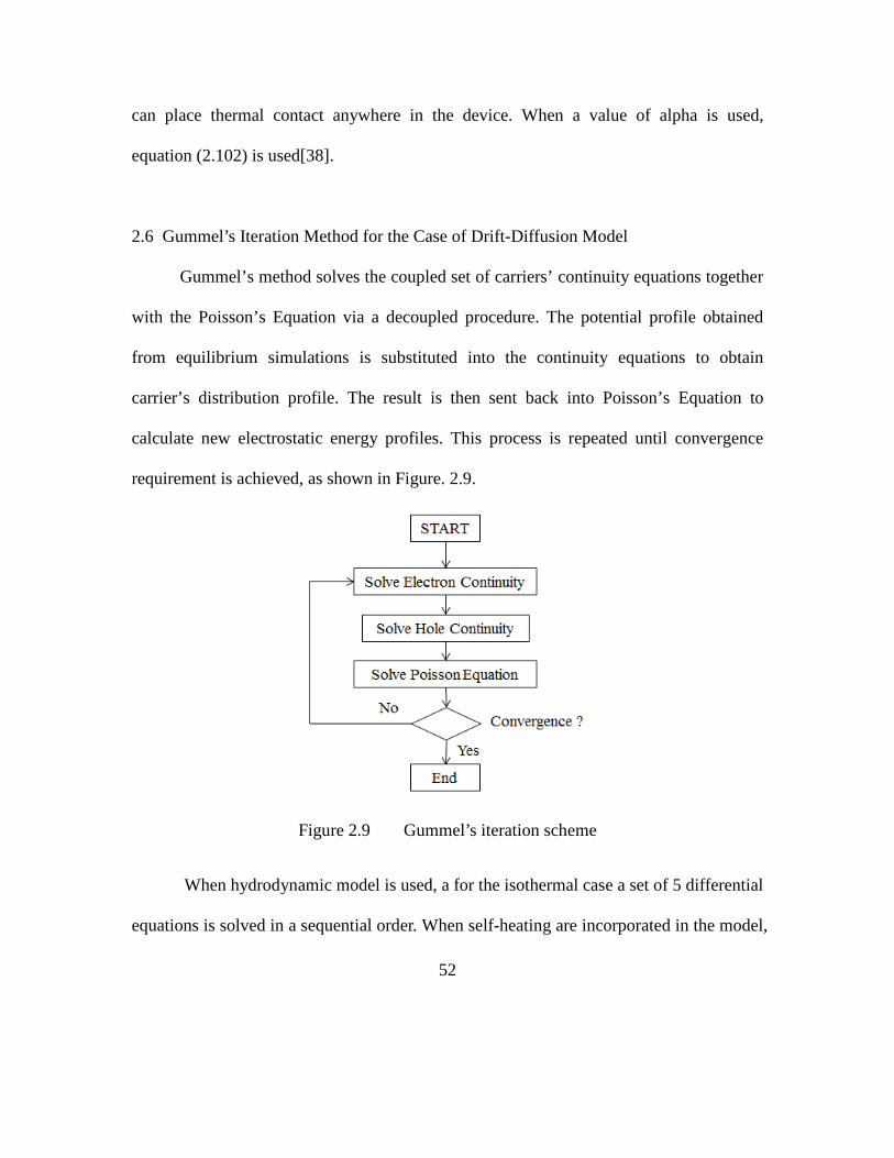
2.6 Gummel’s Iteration Method for the Case of Drift-Diffusion Model
Gummel’s method solves the coupled set of carriers’ continuity equations together
with the Poisson’s Equation via a decoupled procedure. The potential profile obtained
from equilibrium simulations is substituted into the continuity equations to obtain
carrier’s distribution profile. The result is then sent back into Poisson’s Equation to
calculate new electrostatic energy profiles. This process is repeated until convergence
requirement is achieved, as shown in Figure. 2.9.
Figure 2.9 Gummel’s iteration scheme
When hydrodynamic model is used, a for the isothermal case a set of 5 differential
equations is solved in a sequential order. When self-heating are incorporated in the model,

53
an additional (6th) PDE is solved to model the lattice temperature variation.
2.7. Model Development
Several assumptions were made when creating the model. One assumption is the
gate, drain and source contacts in the model are treated as perfect electrical conductors.
The interfaces between the layers were considered ideal with no modeled defects or
surface modifications besides the interface charge to simulate the piezoelectric effect.
First it was attempted to create an electrically accurate 2-dimensional model of the device
using ‘polarization’ function. After several unsuccessful attempts by this researcher using
the ‘polarization’ function to accurately model the electrical effects of a hetero-junction,
an interface charge was inserted at the AlGaN/GaN boundary using ‘interface’ function.
That also did not work. Then the interface charge was implemented by using n doped
AlGaN layer. When combined with a thin GaN region of increased mobility directly
below the AlGaN/GaN junction, the desired effect is achieved. One of the goals of this
research was to model the device in 2-dimensions.
Structuring the model to match the dimensional characteristics of the physical device was
of paramount importance. Such an approach seemed the most logical with the end goal to
eventually use 2-dimensional thermal modeling. The individual values that were most
often modified throughout the model development were AlGaN layer thickness, Gate
Work Function (WF), donor levels in AlGaN and GaN layers, the interface charge at the

54
heterojunction, momentum and energy relaxation rates, the electron mobilities and
saturation velocities in each of the AlGaN and GaN layers. Final values were chosen
through trial and error until the most accurate representation of IV curves was achieved.
Early on in the model development process, the donor levels(concentrations) were
given the most attention. So a variety of layer concentration were modeled to determine
which would give the closest electrical output characteristics to experimental results.
AlGaN thickness did not have a notably strong effect on modeled device performance.
Gate WF had the largest effect on device linearity and drain current over the modeled
bias ranges. A gate WF of 4.73 eV is used to coincide with the generally accepted WF of
a gate contact for a FET. Generally accepted ranges of available extra electrons at the
heterojunction for the piezoelectric and polarization effects of a GaN HEMT are around
1013 cm-2. Therefore, an interface charge near that level was necessary to model the
piezoelectric effect. The 2-dimensional model closely resembled the electrical
characteristics of the experimented device. The gate length in the model is 0.25 microns
between 0.375 to 0.625 microns. Upper thin layer of GaN acts as channel and lower GaN
layer works as substrate.
In this thesis, the Low Field Mobility Model chosen to simulate the device operation is
Parallel Electric Field Dependent Mobility model. The same structure and same model
was used throughout in the simulation. The effects of applying various parameters of
Albrecht’s model and the comparison with high field mobility models have been further
discussed in the ATLAS manual.

55
Through model development several notable discoveries were made based on
intermediate simulation results. GaN layer has most effect on the electrical characteristic
of the device. During thermal simulation using small value of alpha prevents the model
engine from converging and displays much higher maximum channel temperatures while
the simulation is running when compared to a model that will converge with appropriate
alpha value. Another discovery was that the upper GaN model layer representing channel
would be as thin as 0.002 microns and the electrical results were identical over the same
bias conditions reported by experiment. Thermal results were also identical over the same
bias conditions when compared to the experimental model. Conditions at higher bias
were not modeled during this research. One can postulate that decreasing the GaN layer
will have multiple effects at higher bias conditions due to the depletion region necessary
during device operation, but further research would have to be done to support this.
2.8. Importance of Use of Hydrodynamic Transport Model
The current density equations or charge transport models are usually obtained by
applying approximations and simplifications to the Boltzmann Transport Equation. These
assumptions can result in a number of different transport models such as drift-diffusion
model, the Energy Balance Transport Model or the hydrodynamic model.
The simplest model of charge transport is the Drift-Diffusion model. This model
has the attractive feature that it does not introduce any independent variables in addition

56
to ψ, n and p. Until recently drift-diffusion model was adequate for nearly all devices that
were technologically feasible. Drift-Diffusion (DD)transport equations are not adequate
to model overshoot effects. The limitations of the drift-diffusion model arise because the
model does not take into account hot electrons(only the lattice temperature is accounted
for, and not the energy of carriers). Monte Carlo methods involving the solution of the
Boltzmann kinetic equation are the most general approach. The drawback of this method
is the very high computational time required. The hydrodynamic model provides a very
good approximation to these Monte Carlo methods[51].The thermal hydrodynamic model
used in ATLAS solves six PDEs: Poisson, continuity and energy conservation equations
for holes and electrons, plus the lattice temperature equation.

57
Chapter 3 SIMULATION RESULTS
This section describes the simulations performed and the analysis of the
corresponding results for both HEMT structures introduced in Section 2.3.In both cases,
transfer and output I-V characteristics curves were simulated for the isothermal
(excluding self-heating effect) case. Then, transfer and output I-V characteristics curve
were simulated for the nonisothermal (including self-heating effect) case. The
nonisothermal simulation was performed by placing a thermal contact at the bottom of
the substrate which was set to 300K.Lattice temperature profile and Joule heat power
profile were plotted. The ambient temperature at which the model was simulated is 300 K.
All I-V curves were compared with corresponding experimental data.
3.1. AlGaN/GaN HEMT
3.1.1. Isothermal Simulation
3.1.1.1. Transfer Curve
The transfer curve was simulated for Vd=10 V. Shown in figure 3.1 is the transfer
I-V characteristic of Structure 1 being considered. The application of a gate bias greater
than the threshold voltage (which approximately equals -4.2 V) induces a 2DEG
concentration in the channel of the HEMT.
Also shown in this figure are the experimental measurements. Note that the
simulated result closely matches the experimental data. These results correspond to the
isothermal case.

58
Figure 3.1 Comparison transfer I-V curve for AlGaN/GaN HEMT.
3.1.1.2. Output I-V Curve
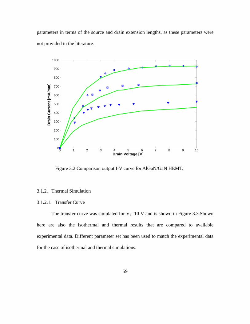
The output I-V curve was plotted for different gate biases: Vg=0V, -1V and -2V
while the drain voltage Vd is ramped from 0 to 10V.The device is biased at a gate voltage
greater than the threshold voltage to induce a channel at a constant drain bias. Shown in
Figure 3.2 are the output characteristics of the structure together with experimental data.
The simulated result closely matches the experimental data for Vg = 0V, but it deviates as
Vg becomes more negative. This can be attributed to the fact that Silvaco does not have
good mobility models for nitride devices. Also, there is an uncertainty in the structure
-6 -5 -4 -3 -2 -1 0 10
100
200
300
400
500
600
700
800
900
1000
Gate Voltage [V]
Cu
rren
t [m
A/m
m]
IsothermalExperimental
59
parameters in terms of the source and drain extension lengths, as these parameters were
not provided in the literature.
Figure 3.2 Comparison output I-V curve for AlGaN/GaN HEMT.
3.1.2. Thermal Simulation
3.1.2.1. Transfer Curve
The transfer curve was simulated for Vd=10 V and is shown in Figure 3.3.Shown
here are also the isothermal and thermal results that are compared to available
experimental data. Different parameter set has been used to match the experimental data
for the case of isothermal and thermal simulations.
0 1 2 3 4 5 6 7 8 9 100
100
200
300
400
500
600
700
800
900
1000
Drain Voltage [V]
Dra
in C
urr
ent
[mA
/mm
]

60
Simulated result shows that there is a reduction in drain current due to
degradation of mobility due to self-heating as well as a change in the slope which would
result in a change in the transconductance.
In Figure 3.4 we show the transfer characteristics when thermal model has been
used as a reference parameter set model.
Figure 3.3 Comparison of transfer I-V curve for AlGaN/GaN HEMT. Different parameter
set is used for isothermal and thermal simulations to match experimental data.
-6 -5 -4 -3 -2 -1 00
100
200
300
400
500
600
700
800
900
1000
Gate Voltage(V)
Cur
rent
[uA
/um
]
Isothermal
Experimental
Thermal
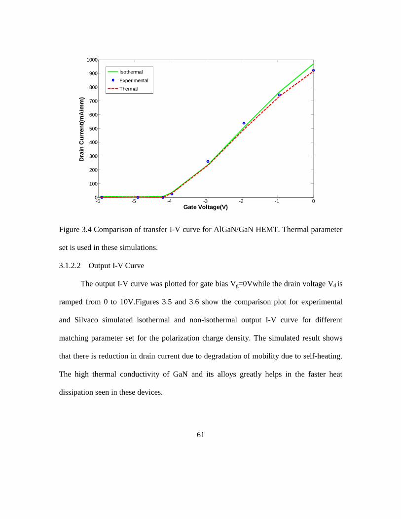
61
Figure 3.4 Comparison of transfer I-V curve for AlGaN/GaN HEMT. Thermal parameter
set is used in these simulations.
3.1.2.2 Output I-V Curve
The output I-V curve was plotted for gate bias Vg=0Vwhile the drain voltage Vd is
ramped from 0 to 10V.Figures 3.5 and 3.6 show the comparison plot for experimental
and Silvaco simulated isothermal and non-isothermal output I-V curve for different
matching parameter set for the polarization charge density. The simulated result shows
that there is reduction in drain current due to degradation of mobility due to self-heating.
The high thermal conductivity of GaN and its alloys greatly helps in the faster heat
dissipation seen in these devices.
-6 -5 -4 -3 -2 -1 00
100
200
300
400
500
600
700
800
900
1000
Gate Voltage(V)
Dra
in C
urr
ent(
mA
/mm
)
Isothermal
Experimental
Thermal

62
Figure 3.5 Comparison of output I-V curve for AlGaN/GaN HEMT for different
parameter sets used for isothermal and thermal simulations.
0 1 2 3 4 5 6 7 8 9 100
100
200
300
400
500
600
700
800
900
1000
Drain Voltage (V)
Dra
in C
urr
ent
[mA
/mm
]
Experimental dataIsothermal SimulationsThermal simulations

63
Figure 3.6 Comparison of output I-V curve for AlGaN/GaN HEMT. Thermal parameter
set is used in these isothermal simulations.
3.1.2.3. Temperature and Joule Heating Profile
Figures 3.7 and 3.8 show the lattice temperature and Joule heat power profile
respectively for gate bias Vg=0V and drain bias Vd=10 V for AlGaN/GaN HEMT. The
lattice temperature profile shows that the hot spot occurs in the gate-drain spacing, right
where the gate terminates, but is restricted closer to the AlGaN/GaN interface. This
means that most of the hot electrons are close to the AlGaN/GaN interface. The profile
also shows that there might be some high energy electrons in the AlGaN barrier layer on
the drain end.
0 1 2 3 4 5 6 7 8 9 100
100
200
300
400
500
600
700
800
900
1000
Drain Voltage (V)
Dra
in C
urr
ent
(mA
/mm
)

64
The mobility degrades rapidly around the hot spot due to high electric fields. This
degradation in mobility causes a reduction in drain current as shown in Figure 3.5.The
temperature around the hot spot reaches a maximum of 337 K.
Figure 3.7 Lattice temperature profile for AlGaN/GaN HEMT.

65
Figure 3.8 Joule heat power profile for AlGaN/GaN HEMT.
3.2. GaN/AlGaN/AlN/GaN HEMT
3.2.1 Isothermal simulation
3.2.1.1 Transfer Curve
The transfer curve was simulated for Vd=5 V. This simulation was done to match
the threshold voltage of the device which is experimentally found to be -3.7 V, and the
on-state current. Substrate and back polarization charges were manipulated for that
purpose. In this structure, the application of a gate bias greater than the threshold voltage
induces a 2DEG concentration in the channel of the HEMT. Figure 3.9 shows the
comparison plot for experimental and Silvaco simulated transfer I-V curve of Structure 2
introduced in Section 2.3.Simulated transfer characteristic closely matches the

66
experimental data. Isothermal situation is considered only. The effect of self-heating is
illustrated in section 3.2.2 below.
Figure 3.9 Comparison transfer I-V curve for GaN/AlGaN/AlN/GaN HEMT.
3.2.1.2. Output I-V Curve
The output I-V curve was plotted for different gate biases Vg=0V,-1V and -2V
while the drain voltage Vd is ramped from 0 to 5V. The device is biased at a gate voltage
greater than threshold voltage to induce a channel at a constant drain bias. Figure 3.10
shows the comparison plot for experimental and Silvaco simulated output I-V curve. The
simulated result closely matches the experimental data for Vg=0 V.
-6 -5 -4 -3 -2 -1 00
100
200
300
400
500
600
700
800
900
1000
Gate Voltage (V)
Dra
in C
urre
nt (
mA
/mm
)
Isothermal
Experimental data

67
Figure 3.10 Comparison output I-V curve for GaN/AlGaN/AlN/GaN HEMT
3.2.2. Non-Isothermal Simulation
3.2.2.1. Transfer Curve
Figure 3.11 shows the comparison plot for experimental and Silvaco simulated
isothermal and non-isothermal transfer I-V curve. The simulated result shows that there is
reduction in drain current due to degradation of mobility due to self-heating. We also
observe change in the slope which results in a change in the transconductance.
0 0.5 1 1.5 2 2.5 3 3.5 4 4.5 50
100
200
300
400
500
600
700
800
900
1000
Drain Voltage (V)
Dra
in C
urre
nt (
mA
/mm
)

68
Figure 3.11 Comparison of transfer I-V curve for GaN/AlGaN/AlN/GaN HEMT.
3.2.2.2. Output I-V Curve
The output I-V curve was plotted for gate bias Vg=0Vwhile the drain voltage is
ramped from 0 to 5V for the non-isothermal case. The device is biased at a gate voltage
greater than threshold voltage to induce a channel at a constant drain bias. Vg = 0 V is
chosen as at less negative gate voltage for which self-heating induced mobility
degradation dominates. Figure 3.12 shows the comparison plot for experimental and
Silvaco simulated isothermal and non-isothermal output I-V curves. The simulated result
shows there is reduction in drain current due to degradation of mobility due to self-
heating. The high thermal conductivity of GaN and its alloys greatly helps in the faster
-6 -5 -4 -3 -2 -1 00
100
200
300
400
500
600
700
800
900
1000
Gate Voltage (V)
Dra
in C
urre
nt (
mA
/mm
)
isothermalexperimentalthermal

69
heat dissipation seen in these devices. Larger current degradations are expected for higher
drain biases.
Figure 3.12 Comparison output I-V curve for GaN/AlGaN/AlN/GaN HEMT
3.2.2.3. Temperature and Joule Heating Profile
Figure 3.13 and Figure 3.14 show the lattice temperature and the Joule heat
power profile respectively for gate bias Vg=0V and drain bias Vd=8 V for
AlGaN/AlN/GaN HEMT. An important parameter related to the reliability of GaN
HEMTs is the lattice temperature profile. It is evident from the figure that the hot-spot is
near the drain end of the channel where the electron temperature is highest and is shifted
slightly towards the drain end on the lattice temperature profile due to the finite group
0 0.5 1 1.5 2 2.5 3 3.5 4 4.5 50
100
200
300
400
500
600
700
800
900
1000
Drain Voltage (V)
Dra
in C
urre
nt (
mA
/mm
)

70
velocity of the acoustic phonons. More importantly, the hot spot extends both towards the
gate and towards the channel. The mobility degrades rapidly around the hot spot due to
high electric fields. This degradation in mobility causes a reduction in drain current. The
temperature around the hot spot reaches a maximum of 320 K. It can be seen reduction in
self-heating away from the hot spot.
Figure 3.13 Lattice temperature profile for GaN/AlGaN/AlN/GaN HEMT.

71
Figure 3.14 Joule heat power profile for GaN/AlGaN/AlN/GaN HEMT.

72
Chapter 4 CONCLUSIONS AND FUTURE WORK
This section summarized the key features of this thesis project and its results,
followed by the plan for future research of GaN HEMTs.
4.1. Conclusions
To conclude, this work has been done for the purpose of understanding thermal
concerns in GaN HEMT technology devices used for high-power and RF applications.
An AlGaN/GaN HEMT hydrodynamic model has been developed utilizing the Silvaco
simulation software that is able to simulate an actual device over a similar range of
measured bias conditions. The spontaneous and piezoelectric polarization effects are
significant in AlGaN/GaN devices and can be modeled with good degree of accuracy
utilizing the Silvaco simulation software. In this work, the desired density of carriers has
been demonstrated to concur with established theory by performing the modeling. Also,
the current versus voltage performance (I-V curves) of the modeled device approximates
experiental results for isothermal case. But still some discrepancy was observed for lower
gate bias. It has been found that there is decrease in drain current due to mobility
degradation as electric field increases due to increase in lattice temperature using the
thermal model. This observation justifies the preference given to high thermal
conductivity substrate materials used in GaN HEMT manufacturing. This study has also
proven that the electrostatics near the gate-drain edge is a very critical for a reliable
performance of these devices. More research needs to be done on GaN HEMTs and that
73
could help in overcoming the unresolved issues and slowly bridging the technological
gap between the GaN and GaAs/Silicon devices.
4.2. Future Work
Although the simulation model developed in this thesis work has been able to
represent the operation of a HEMT device successfully, some of the issues faced during
the work remain unexplained and need to be addressed as future work in order to further
strengthen the reliability of such simulation model.
The model requires greater refinement and treatment to more closely match actual device
performance. Differences were found in the linear region of output I-V characterictics of the
model compared to experimental data. The difference increased as gate voltage was made more
negative(below 0V).Since such a slope represents the on-resistance of the device, it is certain that
resistive behavior was not correctly simulated. Various parameters were changed to solve the
issue. The issue is still open and needs to be investigated further. In addition to this, other
potential methods to resolve the I-V curve discrepancies are interface and quantum effects related
to the device. The Silvaco software TM has an INTERFACE statement that allows one to define
the interface charge density. This function might allow for a simple method for defining the
2DEG but it could modify the surface recombination velocity and thermionic emissions, which
might be undesirable.The quantum effects can be addressed in Silvaco by solving Schrodinger’s
equation, which will modify the normally calculated density of states and carrier concentrations.
Relying on an ATLASTM piezo’ function specifically built for the piezoelectric effect and using
74
constant saturation velocities and electron mobilities would make for a more plausible model at
high frequencies.
The simulations presented here have been done on a standard GaN HEMT with
fixed dimensions of various layers, but the code is capable of modeling GaN HEMT
constructed with varying layer dimensions and substrate material.
To provide a more accurate model from a thermal standpoint more data should be
gathered from a real device while under a variety of measured thermal conditions. This
data could be correlated to simulated data and lead to the use of alternative thermal
functions to provide a more accurate overall model. Another way to increase thermal
accuracy would be to incorporate hot carrier effects into the model. In this research, hot
carrier effects was avoided due to the insufficient amount of time an individual
simulation was taking to converge. By decreasing the amount of mesh points and
simplifying the physical dimensions of the device, the model may converge in a more
tolerable time frame and more functions within ATLASTM could be incorporated. For
these simulations, the trapping effects were not included. It has been reported that the
electrical performances are strongly affected by surface and substrate traps. The trapping
effects can also limit the output power performance of microwave field-effect transistors
(FETs)[52-53].In ATLAS user’s manual[38] various models are introduced to include the
trapping effects. Therefore, a possible next step to improve the modeling would be
including the trapping effects. Although the simulations done using Hydrodynamic model
give close match to experimental data, the difference Monte Carlo model would make

75
remains to be seen. The effect of shielding these devices which may have significant
impact on the reliability issues in these devices has to be investigated.

76
REFERENCES
[1] Frank et al. “Device scaling limits of Si MOSFETs and their application dependencies,” Proceedings of the IEEE , Vol.89, No.3,2001.
[2] T. P. Chow, R. Tyagi, “Wide bandgap compound semiconductors for superior high voltage unipolar devices,” IEEE Trans. Electron Devices, vol. 41, 1481-1483, Aug. 1994.
[3] Y. F. Wu, D. Kapolnek, J. P. Ibbeston, P. Parikh, B. P. Keller, and U.K. Mishra, “Very high power density AlGaN/GaN HEMTs,” IEEE Trans. Electron Devices, vol. 48, 586-590, Mar. 2001.
[4] V. Tilak, B. Green, V. Kaper, H. Kim, T. Prunty, J. Smart, J. Shealy, and L. Eastman, “Influence of barrier thickness on the high power performance of AlGaN/GaN HEMTs,” IEEE Electron Device Lett. , vol. 22, 268-270, Nov. 2001.
[5] S.T. Shepard, K. Doverspike, W.L.Pribble,S.T.Allen J.W.Palmour,L.T.Kehias and T.J Jenkins, “High-Power Microwave GaN/AlGaN HEMT’s on Semi-Insulating Silicon Carbide Substrates ,” IEEE Electron Device Letter ,Vol.20,No 4 pp.161-163,April 1999.
[6] Y. F. Wu, P. M. Chavarkar, M. Moore, P. Parikh, B. P. Keller and U. K. Mishra, “A 50-W AlGaN/GaN amplifier,” Int. Electron devices Meeting, CA, 2000.
[7] T. H. Yu and K. F. Brennan, “Theoretical study of the two-dimensional electron mobility in strained III – nitride heterostructures,” Journ. Of Appl. Phys., vol. 89, 3827-3834, Apr. 2001.
[8] Y. F. Wu, B. P. Keller, P. Fini, S. Keller, T. J. Jenkins, L. T. Kehias, S. P. DenBaars, and U. K. Mishra, Journ. Of Appl. Phys., vol. 19, 50, 1998.
[9] S. Strite and H. Morkoc, “GaN, AlN, and InN: A review,” J. Vac. Sci. Technol B, vol. 10, 1237-1266, Jul. 1992.

77
[10] Eimers, Karl P., “2D Modeling of GaN HEMTs Incorporating the Piezoelectric Effect,” Thesis, Naval Postgraduate School, March 2001.
[11] Manju K. Chattopadhyay and Sanjiv Tokekar, “Thermal model for dc characteristics of AlGaN/GaN HEMTs including self-heating effect and non-linear polarization,” Microelectronics Journal, vol. 39, pp. 1181–1188, 2008.
[12] E.R. Heller and A. Crespo, “Electro-thermal modeling of multifinger AlGaN/GaN HEMT device operation including thermal substrate effects,” Microelectronics Reliability, vol.48, pp.45-50, January 2008.
[13] W.C. Johnson, J. B. Parsons and M.C. Crew, J. Phys. Chem. 36 (1932) 2651.
[14] H.P. Maruska, J.J. Tietjen, Appl. Phys. Lett. 15 (1969) 327.
[15] H. P. Maruska, W. C. Rhines, D. A. Stevenson, “Preparation of Mg-doped GaN diodes exhibiting violet electroluminescence,” Mat. Res. Bull., vol. 7, 777, 1972.
[16] H. Amano, N. Sawaki and I. Akasaki, Y. Toyoda, “Metalorganicvapor phase epitaxial growth of a high quality GaN film using an AIN buffer layer,” App. Phys. Lett., vol. 77, 250-252, Jul. 2000.
[17] M. A. Khan, J. N. Kuznia, J. M. Vanhove, N. Pan, and J. Carter, "Observation of a 2-dimensional electron-gas in low-pressure metalorganic chemical vapor deposited GaN-AlGaN heterojunctions," Applied Physics Letters vol. 60, pp. 3027-3029, Jun 1992.
[18] M. A. Khan, A Bhattarai, J. N. Kuznia, and D. T. Olson, "High-electron-mobility transistor based on a GaN-AlGaN heterojunction," Applied Physics Letters, vol. 63, pp. 1214-1215, Aug 1993.
[19] M. A. Khan, J. N. Kuznia, D. T. Olson, W. J. Schaff, J. W. Burm, and M. S. Shur "Microwave performance of a 0.25 µm gate AlGaN/GaN heterostructure field-effect transistor," Applied Physics Letters, vol. 65, pp. 1121-1123, Aug 1994

78
[20] Y. F. Wu, B. P. Keller, S. Keller, D. Kapolnek, S. P. Denbaars, and U. K. Mishra, "Measured microwave power performance of AlGaN/GaN MODFET," IEEE Electron Device Letters, vol. 17, pp. 455-457, Sep 1996.
[21] B. M. Green, K. K. Chu, E. M. Chumbes, J. A. Smart, J. R. Shealy, and L. F. Eastman, "The effect of surface passivation on the microwave characteristics of undoped AlGaN/GaN HEMT's," IEEE Electron Device Letters, vol. 21, pp. 268-270, Jun 2000.
[22] Yoshiki Kato, Shota Kitamura, KazumasaHiramatsu, Nobuhiko Sawaki, “Selective growth of wurziteGaN and Al1-xGaxN on GaN/sapphire substrates by metalorganicvapor phase epitaxy,” Journ. Of Crystal Growth., vol. 144, 133-140, 1994.
[23] S. J. Pearton, F. Ren, A. P. Zhang, K. P. Lee, “Fabrication and performance of GaN electronic devices,” Materials Science and Engineering: R: Reports., vol. 30, 55-212, Dec. 2000.
[24] Xu, H., C. Sanabria, S. Heikman, S. Keller, U. K. Mishra, and R. A. York. “High Power GaN Oscillators Using Field-Plated HEMT Structure,” (2005): 1345-1348.
[25] Chini, A., D. Buttari, R. Coffie, S. Heikman, S. Keller, and U. K. Mishra. “12 W/mm Power Density AlGaN/GaN HEMTs on Sapphire Substrate.” Electronics Letters 40, no. 1TY - JOUR (2004): 73-74.
[26] O. Ambacher, J. Smart, J. R. Shealy, N. G. Weimann, K. Chu, M. Murphy, W. J. Schaff, and L. F. Eastman, R. Dimitrov, L. Wittmer, and M. Stutzmann, W. Rieger and J. Hilsenbeck, “Two-dimensional electron gases induced by spontaneous and piezoelectric polarization charges in N- and Ga-face AlGaN/GaNheterostructures,” Journ. Of Appl. Phys., vol. 85, 3222-3233, Mar. 1999.
[27] Manju K. Chattopadhyay and Sanjiv Tokekar, ” Thermal model for dc characteristics of AlGaN/GaN HEMTs including self-heating effect and non-linear polarization,” Microelectronics Journal, vol. 39, pp. 1181–1188, 2008.

79
[28] Xing, H. et al., “Gallium Nitride Based Transistors.” J. Phys.: Condens. Matter 13 - JOUR (2001):7139-7157.
[29] Borges, Ricardo, “High Electron Mobility Transistors (HEMT).” internet,www.nitronex.com/education/ganHEMT.pdf, December 2005.
[30] Kenneth L. Holmes, “ Two dimensional modeling of Aluminum Gallium Nitride/Gallium Nitride High electron mobility transistor,”MS thesis, June,2002.
[31] L. Shen, S. Heikman, B. Moran, R. Coffie, N.-Q. Zhang, D. Buttari, I. P. Smorchkova, S. Keller, S. P. DenBaars and U. K. Mishra, “AlGaN/AlN/GaN High-Power Microwave HEMT,” IEEE Trans. Electron Devices, vol. 22, 457-459, Oct. 2001.
[32] T. W. Kima and D. C. Choo, K. H. Yoo, M. H. Jung, Jae-Hoon Lee and Jung-Hee Lee, “Carrier density and mobility modifications of the two-dimensional electron gas due to an embedded AlN potential barrier layer in AlxGa1-xN/GaN heterostructures,” Journ. Of Appl. Phys., vol. 97, 103721, 1-5, May. 2005.
[33] L. Guo, X. Wang, C. Wang, H. Xiao, J. Ran, W. Luo, X. Wang, B. Wang, C. Fang, G. Hu, “The influence of 1 nm AlN interlayer on properties of the Al0.3Ga0.7N/AlN/GaN HEMT structure,” Microelectronics Journal, vol. 39, 777-781, Jan. 2008.
[34] G. Parish, G. A. Umana-Membreno, S. M. Jolley, D. Buttari, S. Keller, B. D. Nener and U. K. Mishra, “AlGaN/AlN/GaN High Electron Mobility Transistors with Improved Carrier Transport,” Optoelectronic and Microelectronic Materials and Devices, 2004.
[35] O. Ambacher, J. Smart, J. R. Shealy, N. G. Weimann, K. Chu, M. Murphy, W. J. Schaff, L. F. Eastman, R. Dimitrov, L. Wittmer, M. Stutzmann, W. Reiger, and J. Hilsenbeck, “Two-dimensional electron gases induced by spontaneous and piezoelectric polarization changes in N- and Ga-face AlGaN/GaN heterostructures,” Journ. of Appl. Phys., vol. 87, 334-344, Jan. 2000.

80
[36] Selberherr, S.Analysis and Simulation of Semiconductor Devices.Wien NewYork:Springer-Verlag,1984.
[37] Lundstrom M. ,and R.Shuelke, “Numerical Analysis of Heterostructure Semiconductor Devices ,”IEEE trans. Electron Devices Vol.30(1983):1151-1159.
[38] Silvaco Inc. , “ ATLAS User’s Manual Device Simulation Software,” August,2011.
[39] Stratton, R.,Phys.Rev.,126 ,6(1962):2002.
[40] Stratton, R,. “ Semiconductor Current-Flow Equations(Diffusion and Degeneracy,” IEEE Trans. ,Electron Devices Vol.19, No.12(1972):1288-1292.
[41] Meinerzhagen, B.,K. Bach, I. Bozk, and W.L.Eugl, “ A New Highly Efficient Nonlinear Relaxation Scheme for Hydrodynamic MOS Simulation,”Proc.NUPAD IV(1992):91.
[42] Apanovich Y.el.al, “Numerical Simulation of Submicron Devices, Including Coupled Non-local Transport and Non-isothermal effects,” IEEE trans. Electron Devices Vol.42, No.5(1995):890-898.
[43] Apanovich Y.el.al, “Steady-State and Transient Analysis of Submicron Devices Using Energy Balance and Simplified Hydrodynamic Models,” IEEE trans. Comp. Aided Design of Integrated Circuits and SystemsVol.13, No.6(June 1994):702-710.
[44] B.G. Streetman and S. Banerjee , “Solid State Electronic Devices,” Vol.2: Prentice-Hall Englewood Cliffs, NJ, 1995.
[45] Rhoderick , E.H.and R.H. Williams , “ Metal Semiconductor Contacts,” 2nd edition,Oxford Science Publications, 1988.
[46] Caughey , D.M., and R.E. Thomas , “Carrier Mobilities in Silicon Empirically related to Doping and Field,” Proc. IEEE 55,(1967),:2192-2193.

81
[47] Schwarz, S.A., and S.E. Russe , “ Semi-Empirical Equations for Electron Velocity in Silicon: Part II-MOS inversion Layer,” IEEE Trans. Electron Devices Vol.30, No 12(1983):1634-1639.
[48] Wachutka , G.K., “Rigorous Thermodynamic Treatment of Heat Generation in Semiconductor Device modeling,”IEEE Trans. Computer –Aided Design , Vol.9, No.11,(1990):1141-1149.
[49] Herring , C. “ Theory of the Thermoelectric Power of Semiconductors ,”Phys. Rev., Vol 96, (Dec 1954) : 1163-1187.
[50] Geballe T.H. ,T.W. Hull, “ Seebeck Effect in Silicon, “Phys. Rev., Vol 98, ( 1955)940-947.
[51] K.Blotejka ,“ Transport equations for electrons in 2 valley –semiconductors,” IEEE Transactions on Electronic Devices, vol. Ed 17,pp.38-& ,1970.
[52] Steven C. Binari ,P. B. Klein and Thomas E. Kazior,” Trapping effects in GaN and SiC microwave FETs,” Proceedings of the IEEE, vol.90, pp.1048-1058, June 2002.
[53] S. Augaudy, R. Quere, J.P. Teyssier, M.A. Di Forte-Poisson, S. Cassette, B. Dessertenne and S.L Delage,” Pulse characterization of trapping and thermal effects of microwave GaN power FETs,” Microwave Symposium Digest, vol.1,pp. 427-430, May 2001.