study of demolding process in thermal imprint lithography
TRANSCRIPT

Louisiana State UniversityLSU Digital Commons
LSU Master's Theses Graduate School
2007
Study of demolding process in thermal imprintlithography via numerical simulation andexperimental approachesZhichao SongLouisiana State University and Agricultural and Mechanical College, [email protected]
Follow this and additional works at: https://digitalcommons.lsu.edu/gradschool_theses
Part of the Mechanical Engineering Commons
This Thesis is brought to you for free and open access by the Graduate School at LSU Digital Commons. It has been accepted for inclusion in LSUMaster's Theses by an authorized graduate school editor of LSU Digital Commons. For more information, please contact [email protected].
Recommended CitationSong, Zhichao, "Study of demolding process in thermal imprint lithography via numerical simulation and experimental approaches"(2007). LSU Master's Theses. 2965.https://digitalcommons.lsu.edu/gradschool_theses/2965

STUDY OF DEMOLDING PROCESS IN THERMAL IMPRINT LITHOGRAPHY VIA NUMERICAL SIMULATION AND
EXPERIMENTAL APPROACHES
A Thesis
Submitted to Graduate Faculty of the Louisiana State University and
Agricultural and Mechanical College in partial fulfillment
of the requirements for the degree of Master of Science in Mechanical Engineering
in
The Department of Mechanical Engineering
by Zhichao Song
B.S, University of Science and Technology of China, Hefei, China, 2005 December, 2007

ii
To my parents, family and friends

iii
Acknowledgements
I would like to express my sincere thanks to all the people who have been helped me in my
success throughout my master’s program here at Louisiana State University.
It is my great pleasure to be guided, motivated and supported by Dr. Sunggook Park, who is
always available to me for any research related discussion, no matter how busy he is. Thank my
advisor for introducing me to the field of nanoimprint lithography and educating me to become a
qualified researcher.
Thanks are extended also to Dr M.C. Murphy and Dr D. E. Nikitopoulos for being my
committee members and for their time and expertise to evaluate the thesis.
I thank all my colleagues in Nanosystem Laboratory for their technical assistance. Special
thanks to Veronica and Lance for their assistance in demolding test. It is almost impossible for me
to fulfill the experimental part of my thesis in time without their help.
I also thank Jing Jiang, a senior graduate student in ME department, for fruitful discussion
and tremendous help on contact simulation in ANSYS.
It is time to mention about my friends, Fei Wang, Limin Xiao and Fan Huang. I clearly
remember those days we had fun together and I could not image how dull and difficult my life
would be without you guys.
Finally, I would like to acknowledge the love of my parents Changyin Song and Lanlin Lu
for their support and encouragement all my school days.

iv
Table of Contents
ACKOWLEDEGMENTS............................................................................................................iii
LIST OF TABLES………...............................................................................................................vii
LIST OF FIGURES……................................................................................................................viii
ABSTRACT.......................................................................................................................................xi
CHAPTER 1. INTRODUCTION……………………………………………….............................1 1.1 General Background……………………………..………………………....................................1 1.2 Goal and Objectives of this study……………………..…………………....................................3 CHAPTER 2. LITERATURE SURVEY..........................................................................................5 2.1 Thermal Imprint Lithography Process ……………......................................................................6 2.1.1 Development of Thermal Imprint Lithography and Its Variants.......................................... 7 2.1.2 Application of Thermal Imprint Lithography......................................................................10 2.1.2.1 Biological Application............................................................................................10 2.1.2.2 Polymer Photonic Device.......................................................................................11 2.2 Polymer Flow Behavior in Molding............................................................................................12 2.2.1 Experimental Study on Polymer Flow Behavior in Molding………….............................13 2.2.2 Simulation Study on Polymer Flow Behavior in Molding.................................................15 2.3 Study of the Demolding Process..................................................................................................18 2.3.1 Surface Treatment – Anti Adhesion Coating......................................................................18 2.3.2 Demolding Simulation and Experimen...............................................................................20 CHAPTER 3. SIMULATION METHODOLGY..........................................................................23 3.1Mold Creation...............................................................................................................................23 3.1.1 Boundary Conditions and Load Setting...............................................................................24 3.1.2 Element Type and Meshing Detail.......................................................................................25 3.2 Material Properties.......................................................................................................................25 3.2.1 Silicon – Linear isotropic elastic model...............................................................................25 3.2.2 PMMA – Viscoelastic Model...............................................................................................25 3.2.2.1Viscoelasticity...........................................................................................................26 3.2.2.2 Molecule Background..............................................................................................26 3.2.2.3 10-Element Maxwell Model....................................................................................27 3.2.2.4 Time-Temperature Superposition and Williams-Landel-Ferry (WLF) Equation.................................................................................................................. 29 3.2.2.5 Equation of State......................................................................................................31 3.3 Process Assumptions....................................................................................................................33 3.4 Governing Equations...................................................................................................................36 3.4.1 Continuity Equations…......................................................................................................36 3.4.2 Navier-Stokes Momentum Equations..................................................................................36

v
3.4.3 Strain-Displacement Equations…………............................................................................37 3.4.4 Strain Compatibility Equations............................................................................................37 3.5 Contact Algorithm .......................................................................................................................38 CHAPTER 4. DEMOLDING SIMULATION IN THERMAL NIL............................................40 4.1 Introduction..................................................................................................................................40 4.2 Mechanical Behavior of PMMA Resist during Normal Demolding…………………...............40 4.2.1 Stress Analysis in Noraml Demolding for Stamp of Single Symmetric Structure.............40 4.2.2 Stress Analysis in Noraml Demolding for Stamp of Multiple Symmetric Structure…......43 4.3 Parametric Study of Demolding...................................................................................................45 4.3.1 Influence of Demolding Angle............................................................................................45 4.3.2 Influence of Demolding Rate..............................................................................................46 4.3.3 Influence of Friction Coefficient.........................................................................................49 4.3.4 Influence of Demolding Temperature.................................................................................51 4.3.5 Influence of Stamp Aspect Ratio........................................................................................54 4.4Conclusions...................................................................................................................................56 CHAPTER 5. EXPERIMENTAL STUDY OF DEMOLDING PROCESS IN THERMAL NIL....................................................................................................................................................58 5.1Introduction...................................................................................................................................58 5.2 Experimental Details....................................................................................................................58 5.2.1 Stamp Fabrication...............................................................................................................59 5.2.1.1 Photomask Design..................................................................................................59 5.2.1.2 Photolithography.....................................................................................................59 5.2.1.3 Reactive Ion Etching………....................................................................................61
5.2.2 Surface Treatment – Anti Adhesion Coating.......................................................................64 5.2.3 Thermal Imprint Lithography..............................................................................................67 5.2.3.1 Spin Coating............................................................................................................68 5.2.3.2 Thermal Imprinting..................................................................................................68 5.2.4 Demolding Experiment........................................................................................................69 5.2.4.1 Standard Mechanical Tester.....................................................................................70 5.2.4.2 Fabrication of Vacuum Chuck..................................................................................71 5.2.4.3 Temperature Control System...................................................................................73 5.3 Result and Discussion................................................................................................................. 75 5.3.1 General Force-Displacement Response during Demolding................................................75 5.3.2 Influence of Demolding Temperature…………………………….....................................78 5.3.3 Inspection of Imprinted PMMA Patterns............................................................................79 5.3.4 Comparison with Demolding Simulation...........................................................................80
CHAPTER 6. FEM SIMULATION FOR UV IMPRINT............................................................83 6.1 Introduction..................................................................................................................................83 6.2 Volumetric and Mechanical Properties…………........................................................................85 6.3 Finite Element Method Model and Preliminary Theoretical Analysis………............................85 6.4 Simulation Results of Solidification in UV Imprint....................................................................87 CHAPTER 7. DEMOLDING SIMULATION FOR INJECTION MOLDING.........................90

vi
7.1 Introduction..................................................................................................................................90 7.2 Simulation Methodology and Results..........................................................................................93 7.2.1 2 Dimensional FEM Model................................................................................................93 7.2.2 Mesh Sensitivity..................................................................................................................94 7.2.3 Process Assumptions...........................................................................................................95 7.2.4 Material Properties..............................................................................................................96 7.2.5 Simulation...........................................................................................................................96 7.2.6 Stress Distribution in Polycarbonate after Cooling............................................................97 7.2.7 Stress Evolution during Demolding...................................................................................99 7.3 Effect of Friction Coefficient.......................................................................................................99 7.4 Stress Evolution with Modified Mold Insert.............................................................................102 7.5 Dependence on Size and Shape of Modified Structure.............................................................106 7.6 Conclusions................................................................................................................................109 CHAPTER 8 CONCLUSIONS AND FUTURE WORK……………………………………....111 8.1 Summary....................................................................................................................................111 8.2 Conclusions................................................................................................................................111 8.3 Future Work................................................................................................................................114 REFERENCES...............................................................................................................................116 VITA................................................................................................................................................120

vii
List of Tables Table 3.1 Elastic modulus and relaxation time for each Maxwell model in the simulation..............30 Table 4.1 Table 4.1 Temperature dependence of yield stress of PMMA and friction coefficient between PMMA and silicon...............................................................................................................52 Table 5.1 Detail Information on pattern layout of photomask...........................................................60 Table 7.1 Material properties of brass and polycarbonate used in simulation...................................96

viii
List of Figures Figure 2.1 Schematic of thermal imprint lithography..........................................................................7 Figure 2.2 (a) Typical imprint failures of imprinted PMMA patterns and (b) silicon stamp.............19 Figure 3.1 2D finite element method (FEM) model of a Si stamp/PMMA resist/Si substrate assembly............................................................................................................23 Figure 3.2 Schematic of Maxwell model (linear combination of spring and dashpot)..................... 28 Figure 3.3 A Schematic of Generalized Maxwell model ..................................................................29 Figure 4.1 (a) Von Mises stress evolution in PMMA resist during normal demolding for stamp of single symmetric structure and (b) the highest local stress versus demolding time for two location of stress concentration.................................................................................42 Figure 4.2 (a) Von Mises stress evolution in PMMA resist during normal demolding for stamp of
multiple symmetric structure and (b) the highest local stress versus demolding time for three different locations.....................................................................................................44
Figure 4.3 The highest local stress as a function of demolding time for different demolding angles... ...........................................................................................................................................47 Figure 4.4 The highest local stress as a function of demolding angle for first and second maximum
in the highest local stress for different demolding angles............................................... 47 Figure 4.5 The highest local stress as a function of demolding displacement for different demolding rates...................................................................................................................................48 Figure 4.6 Normalized Von Mises stress distribution for non-normal demolding at first maximum And different demolding rates...........................................................................................49 Figure 4.7 The highest local stress verse the demolding time for the demolding process with
different friction coefficient on interface (μ=0.1, 0.2, 0.3) .............................................50 Figure 4.8 Von Mises stress distribution at the first maximum for different demolding temperature (maximum stress in PMMA resist marked) ......................................................................53 Figure 4.9 The highest local stress as a function of demolding time (yield stress highlighted) ......................................................................................................................54 Figure 4.10 Normalized Von Mise stress distribution in PMMA domain at the first maximum for different demolding temperature.....................................................................................54

ix
Figure 4.11 Maximum Normalized Von Mises Stress vs. Demolding Temperature..........................55 Figure 4.12 The highest local stress as a function of the depth ratio at the first maximum in the highest local stress versus demolding time curve for different depth ratios..................56 Figure 5.1 AutoCAD pattern for the mask with line gratings and dot array......................................60 Figure 5.2 Schematic of photolithography.........................................................................................61 Figure 5.3 Silicon etching profile for different recipes (a) (CF4 90s + SF6 25s)×3; (b) (CF4 150s + SF6 25s)×3; (c) (CF4 240s + SF6 25s)×3........................................................................65 Figure 5.4 A schematic of silane coating on silicon surface..............................................................66 Figure 5.5 Water contact angle on a silicon wafer before and after silane coating............................67 Figure 5.6 Water contact angle on silicon wafer as a function of coating time.................................68 Figure 5.7 Obducat 6 inch nanoimprit system...................................................................................69 Figure 5.8 Imprinted PMMA patterns of line gratings with 9μm width and 18μm period................69 Figure 5.9 1000× class modulus cleanroom......................................................................................70 Figure 5.10 Automatic demolding unit based on a standard mechanical tester.................................71 Figure 5.11 (a) Side view of the brass vacuum chuck and (b) Top view of AutoCAD design of vacuum chuck................................................................................................................72 Figure 5.12 Cable connection insider the temperature control box...................................................73 Figure 5.13 A block diagram of a PID controller...............................................................................74 Figure 5.14 (a) force vs. time curve during demolding and (b) the determination of demolding Force..............................................................................................................................76 Figure 5.15 4 measurements of force-displacement curve at 25 ºC and 0.3 µm/s............................78 Figure 5.16 (a) Contact force vs. extension at different demolding temperature and (b) demolding force vs. demolding temperature.................................................................79 Figure 5.17 Imprinted PMMA patterns (line gratings) at different demolding temperature of (a) 25ºC, (b) 70ºC and (c) 100ºC....................................................................................81 Figure 6.1 Schematic of Step and flash imprint lithography (UV Imprintlithography) ...................84
x
Figure 6.2 2D finite element method (FEM) model of stamp/photoresist/substrate assembly..........86 Figure 6.3 Schematic of volumetric shrinkage during solidification.................................................87 Figure 6.4 Von Mises stress distribution in UV resist after solidification for different volumetric shrinkage (mark the highest local stress in each figure) ..................................................88 Figure 6.5 the highest local stress as a function of volumetric shrinkage.........................................88 Figure 7.1 Schematic and equipment of injection molding [Courtesy of B. You et al] ....................90 Figure 7.2 2 dimensional FEM model for cooling and demolding simulation..................................94 Figure 7.3 Shear stress versus the path indicated in the inset for different numbers of mesh in order to verify the mesh Convergence..............................................................................95 Figure 7.4 Shear stress distribution in Polycarbonate after cooling................................................100 Figure 7.5 Shear stress evolution during demolding process (without friction) .............................101 Figure 7.6 Shear stress evolution during demolding process for the outmost micropost (with friction coefficient of 0.3) .....................................................................................102 Figure 7.7 The highest local stress versus demolding time for the three microposts located
(a) 300 mm, (b) 200 mm, and (c) 100 mm from the symmetric center............................103 Figure 7.8 2-D FEM model for modified mold insert with a draft angle........................................104 Figure 7.9 Shear stress distribution after cooling (modified mold insert) ......................................105 Figure 7.10 Shear stress evolution during demolding process (modified mold insert) ..................106 Figure 7.11 The highest local stress as a function of demolding time for original and moldified mold insert....................................................................................................107 Figure 7.12 Shear stress distribution after cooling for PC molded with (a) original mold insert, modified with 50 μm width draft angle (c) 100 μm width draft angle (d) 200 μm width draft angle, and (e) 50 μm radius round corner...............................108 Figure 7.13 The highest local stress as a function of draft angle size..............................................108

xi
Abstract
The objective of present study was to analyze the mechanical behavior of polymer resist
during the demolding process, such as stress distribution and evolution; distortion and tilt of
microstructures in thermal imprint lithography, a new emerging technique in mass production of
micro/nanoscale patterns. One of the most challenging technical issues for thermal imprint
lithography is the structural damages during demolding process. Thermal stress, adhesion force and
friction force all play important roles in determination of the success of demolding and it is crucial
to understand the underlying physics in order to optimize the structure and process design.
In present study, we first studied the stress and deformation behavior of polymer during
demolding by commercial finite element method (FEM) software ANSYS 10.0. Based on plane
stress assumption, a 2-D model was created to represent one segment of the periodic structure. A 10
element Maxwell model was employed to describe the viscoelasticity of polymer resist. The normal
demolding process was simulated and local stress was found to be concentrated at two locations:
the corner of transition zone between patterns and residual layer and the contact region between
patterns and releasing stamp. Parametric study was conducted and the influence of demolding angle,
demolding rate, demolding temperature, friction coefficient and stamp geometry were all identified.
To verify the simulation results, we measured the force required to separate stamp from
substrate (demolding force) at three different temperatures (25ºC, 70ºC and 100ºC) and the lowest
value was shown at 70ºC, which implied the lowest mechanical resistance. Scanning electronic
microscopy (SEM) images also confirmed that the imprinted patterns showed both better overall
quality and sharper local profiles at 70ºC, which showed good agreement with simulation results.
In addition, we extended the FEM simulation to the demolding process of UV imprint
lithography and injection molding. In UV imprint lithography, the residual stress was shown much

xii
lower than the thermal imprint lithography; in injection molding, we predicted that local shear
stress can be reduced up to 25% by building a 10 μm, 45ºdraft angle structure.
Chapter 1 Introduction
1.1 General Background
Micro/nanofabrication commenly refers to an ensemble of technologies used to
fabricate structures at small scale (1-10000 nm), which can be integrated into complicated
hierarchical systems. One of the most important micro/nanofabrication technologies is
lithography, which enables the transformation of micro/nanoscale patterns to certain substrate,
such as silicon, metal, polymer. Conventional lithographic methods, such as electron beam
lithography, focused ion beam lithography, optical projection lithography, extreme UV
lithography and X-ray lithography, have been widely used in the fabrication of integrated
circuit (IC) chips [Guo et al., 2004], biomedical analytical instrumentation [Chen et al., 2001],
polymer photonic devices [Guo et al., 2004] and so on; however, there are a lot of issues yet
to be solved in these methods like the resolution; the cost of these conventional lithographic
methods is also extremely high for most potential users. Thus, it is difficult to commercialize
these conventional lithographic methods for the fabrication of micro/nano-electromechanical
system (MEMS/NEMS) devices.
Recently, several alternative lithographic methods have been investigated, including
microcontact printing, atomic force microscope (AFM) lithography, dip-pen lithography and
nanoimprint lithography (NIL). Among them, nanoimprint lithography (NIL), which was
firstly proposed by Chou’s group in 1995, has been put as one of the 10 emerging
technologies that are likely to change the world, by MIT’s Technology Review, for its high
resolution, high throughput and low cost. It has been illustrated that NIL has the capability of
patterning sub-10 nm features in a thin layer of polymer resist [Chou et al., 1997], which is

- 2 -
much higher than traditional optical lithography. Large area pattern replication has also been
realized by nanoimprint lithography and its in-parallel replication greatly improved the
throughput, comparing with E-beam lithography [Heidari et al., 2000].
Despite the huge advantages, a couple of technical challenges remain in the NIL
process: first, how to deform the polymer resist easily and fill micro/nanostructures on the
stamp efficiently; second, how to reduce the mechanical resistance of separating the stamp
from substrate, thus minimize the likelihood of structural damages.
The first issue is critical to the accuracy of pattern replication and the yield of the
process can be enhanced by fast filling. The physical process involves polymer rheological
behavior at elevated temperature, micro/nanoscale heat transfer, viscous driven and capillary
driven flow and so on. Several groups have worked on the first issue. Polymer flow behavior
was investigated by both experiments [Heydermann et al., 2001] and numerical simulation
[Jeong et al., 2001]. Cavity filling modes were found and the underlying physics was studied
for a better understanding of the process [Jeong et al., 2001; Rowland et al., 2004].
Parametric study was also performed for optimal process design, which enables fast
replication of high quality patterns.
The second issue is criucial for the success of the NIL since most of imprint failures
occur at the demolding stage and all-level mechanical and chemical interactions, such as
thermal stress, adhesion and friction, chemical bonding involve and may contribute to the
imprint failures. However, the study on the second issue is still lacking. Though some
preliminary work has been done in this area recently [Worgull et al., 2005; Guo et al., 2007],
fundamental study and systematic investigation of demolding, a process of separating the

- 3 -
stamp from substrate by overcoming all-level chemical and mechanical interactions between
stamp and substrate formed by the process history and properties of materials involved.
1.2 Goal and Objective of This Study
The primary goal of this study was to study the mechanical behavior of imprinted
poly(methyl methacrylate) (PMMA) resist during demolding in thermal imprint lithography.
Basic rules of stress distribution and evolution were extracted from the results of finite
element method (FEM) simulation and explained in the light of viscoelastic properties of
PMMA and geometrical singularity of stamp. We investigated the influence of several
process and geometrical parameters including demolding temperature, demolding rate,
demolding angle and stamp aspect ratio. The influence of demolding temperature was studied
by experiment and the results showed good agreement with simulation. Furthermore, we
extended the simulation to the study of the ejection process in injection molding and the
demolding process in step and flash lithography. For the injection molding, shear stress
concentration and visible distortion of replicated polycarbonate microposts were observed.
Particularly, we focused on the effect of mold insert geometries on stress concentration.
Based on the simulation results, we predicted that stress in molded PC microposts could be
significantly reduced by modifying sharp corners of the positive features on mold insert with
a draft angle and the size and geometric dependence of the draft angle were analyzed. For
step and flash lithography, simulation results showed much lower stress concentration than
thermal imprint lithography, with identical stamp geometry.
In this thesis, we first gave a brief introduction of the basic background and major
work of the thesis in chapter 1. Following the introduction chapter, we reviewed several

- 4 -
important researches which have been done in related fields in chapter 2. In chapter 3,
simulation methodology including governing equations, FEM modeling, material properties,
and contact algorithm was discussed in detail. Chapter 4 and chapter 5 focused on the study
of demolding in thermal imprint lithography from simulation and experiment, respectively.
Simulation work was extended to study the demolding process in step-and-flash lithography
and ejection process in injection molding in chapter 6 and chapter 7. Finally, we summarized
the work of the thesis and proposed some future work in chapter 8.

- 5 -
Chapter 2 Literature Survey
Thermal imprint lithography, also known as thermal-nanoimprint lithography (NIL)
was firstly proposed by Chou’s group [Chou et al., 1995, 1996]. It has been regarded as one
of the most promising techniques in mass production of micro- and nanoscale patterns.
Compared to the conventional lithographic methods, thermal imprint lithography has shown
great advantages in following aspects. First, since patterns are transferred by the mechanical
deformation of the polymer resist, the resolution of thermal imprint lithography is completely
free from the limitations of conventional lithographic methods, such as light diffraction, beam
scattering, and interference [Guo et al., 2001]. Second, as an in-parallel fabrication approach,
thermal imprint lithography has shown incomparable advantages in pattern replication
efficiency. Recently, large area of patterns (6 inch diameter wafer) with feature sizes down to
50 nm, separated by several hundreds of nanometers from the next feature has been imprinted
[Heidari et al., 2000]. Despite several technical challenges remaining, the “in parallel”
imprinting technique conceptually beats conventional “in sequence” lithography, which are
both expensive and time-consuming. Third, different kinds of thermoplastic polymer and co-
polymer are widely used as the resist layer in thermal imprint lithography. The commercial
availability and low price of these polymers and co-polymers make thermal imprint
lithography a cost-efficient lithographic method for mass production and the biocompatibility
of polymer enables great potential in the biological applications [Guo et al., 2001].
Since the mid 1990s, numerous researches have been performed to improve thermal
imprint lithography and various variants are developed [Chou et al., 1995; Colburn et al.,
1999]. Meanwhile, for better understanding of the physical process of thermal imprint

- 6 -
lithography, several groups focused on the fundamental study on the mechanical behavior of
resist during the molding and demolding process [Heyderman et al., 2000; H. D. Rowland et
al., 2004]. Both experimental and numerical approaches have been employed; several rules
and mechanisms of deformation and stress distribution were extracted, and underlying
physics was discussed. Numerical simulation, particularly finite element method (FEM) has
been proved to be a powerful tool in predicting the stress and deformation behavior of
material at micro/nano scale [Hirai et al., 2001].
In this chapter, we review several significant advances of thermal imprint lithography
(NIL) as well as its variants. Typical applications, like biological applications, polymer
photonic device, are briefly introduced. We also focus on the previous researches in the study
of polymer flow behavior during molding and defect analysis during demolding, which are
closely related to the work presented in the thesis.
2.1 Thermal Imprint Lithography Process
The process of thermal imprint lithography is schematically shown in Figure 2.1. It
consists of three steps: molding (include preheating), cooling, demolding, which altogether
determine the accuracy of pattern replication and strength of replicated patterns. During the
molding step, a stamp with desired micro/nano structures is pressed into a substrate coated
with a thin layer of polymer resist, which is heated above its glass transition temperature.
After conformal molding, the stamp/resist/substrate assembly is cooled down below the glass
transition temperature of the resist, with pressure hold. Finally, the pressure is released and
the stamp is separated from the replicated patterns.

- 7 -
2.1.1 Development of Thermal Imprint Lithography and Its Variants
Chou et al. initially proposed the technique of compression molding in a thin resist
coated on substrate by hard mold insert, followed by anisotropic etching to transfer pattern
through the entire resist thickness. Combine with a lift-off process, metal patterns with a
feature size of 25 nm and a period of 70 nm were fabricated. This work was published in
Science in 1996, in which Chou et al. predicted the great potential of thermal imprint
lithography as a high throughput lithographic method for manufacturing integrated circuits
and other nanodevices. They also pointed out sub-10-nanometer resolution can be achieved
by further development [Chou et al., 1995; Chou et al., 1996].
In 1997, Chou et al. further developed the thermal imprint lithography. They
fabricated 10 nm diameter and 40 nm period holes in PMMA on gold and silicon substrate,
and 6 nm diameter and 65 nm period holes in PMMA on silicon substrate. With this new
technique, they fabricated nanocompact disks with 10 nm features and 400 Gb/in2 data
density, which is three orders of magnitude higher than current CDs and they read back the
Figure 2.1 Schematic of thermal imprint lithography
- 8 -
data successfully by a silicon scan probe [Chou et al., 1997].
In thermal imprint lithography, polymer resist layer needs to be heated above its glass
transition temperature so that the polymer can be deformed easily. However, due to the
mismatch of thermal expansion coefficients, thermal stress is generated during the cooling
process, which may lead to structural failures. Also, the high molding temperature results in
inevitable long thermal cycle time. Khang et al. developed a room-temperature thermal
imprint lithography based on solvent sorption treatment on polymer resist layer [Khang et al.,
2000]. Instead of heating the polymer above its glass transition temperature, they added
solvent to the polymer to reduce the viscosity of the polymer, experiment results showed that
the mold features and imprinted features have the identical size and no patter distortion is
inspected.
Application of hard mold insert has the key advantage of high resolution, however,
the high pressure required to deform the resist may lead to the fracture of mold and substrate.
In order to prolong the lifetime of mold insert and ensure the pattern quality, Khang et al.
used a flexible film (~100μm) mold made of fluoropolymer material with the surface energy
as low as 15.6dyn/cm. SEM and AFM images of polymer surface imprinted were taken to
check the uniformity of pattern depth at four different regions on the sample and result
showed excellent uniformity of 147±3 nm [Khang et al., 2004].
Another well-known variant of thermal imprint lithography, developed by Willson’s
group, in University of Texas, Austin, is called step-and-flash imprint lithography (SFIL) [M.
Colburn et al., 1999]. In the SFIL process, an organic transfer layer is firstly coated on
substrate. Then, a surface treated, transparent template with pattern structures is closely

- 9 -
aligned to the substrate. Once in proximity, a drop of low viscosity, photpolymerizable,
organsilicon solution is introduced into the gap, which is filled by the capillary action of the
solution. After contact, the structure is exposed to UV light, which cures the photopolymer
and creates a solidified, silicon rich replica with low surface energy. Finally, the template is
separated from substrate after UV curing is completed. Compare to thermal imprint
lithography developed by Chou’s group, the SFIL process is implemented at room
temperature and requires low pressures only up to100 KPa. Experimental results have shown
excellent pattern fidelity with resolution down to 60 nm.
For micro- and nanopatterning on functional polymers, low molding temperature and
operation pressure is often desirable. To slove these problems, polymer inking, which is
known as a reverse-nanoimprint lithography, was reported by Bao et al. in 2003. They spin
coated a thin polymer film on a patterned mold on selective surfaces by different type of
surface coating. Then under suitable temperature and pressure condition, the polymer on
protruded surfaces of mold was transferred to the substrate and a positive image of the mold
was obtained [Bao et al., 2003].
Recently, Gao et al. proposed a novel imprint method, air cushion press (ACP) [Gao
et al., 2006]. Compare to widely used method, solid parallel plates press (SPP), air cushion
press showed much better pressure uniformity. Through comparison experiment, air cushion
press shows immunity to backside dust and minimizes the affected area of the dust particles
trapped between substrate and stamp; while solid parallel plate press showed tremendous
stress concentration in the cases above. And compare to solid parallel plates press, air cushion
press has much smaller thermal mass, thus faster the imprint process.

- 10 -
2.1.2 Application of Thermal Imprint Lithography
The high resolution, high throughput and cost-efficient capability of thermal imprint
lithography enable it to be widely used in both academic and industrial applications, which
require precise patterning. In this section, we briefly introduce several of the new applications.
2.1.2.1 Biological Application
It is well known that the reduction in sizes and volumes in miniaturized bio-systems
such as “lab-on-a-chip” can improve the efficiency, throughput and cost dramatically, thus
help the biological applications, such as diagnostics and drug screening, also the research on
genomics and proteomics. The key issue is how to fabricate micro- and nanofluidic devices in
order to minimize the bio-systems. Even though traditional, silica-based microfabrication
process can be used, the intrinsic disadvantages like the high cost and complicated procedure
determine that it cannot be widely used. However, as an emerging high resolution, high
throughput and low cost lithographic method, thermal imprinting based technique may play
an important role in fabrication of micro- and nanofluidic devices as well as direct molding in
polymers.
Guo et al. imprinted a nanochannel template into a very thin layer of resist, which is
coated on a cover slip [Guo et al., 2003]. Because of the limitation of resist supply, structures
on the nanochannel are not completely filled and enclosed channel structures are built. By
controlling the initial thickness of polymer resist layer, enclosed channels with desired size
can be achieved.
Falconnet et al. combined nanoimprint lithography (NIL) and molecular assembly
patterning by lift-off (MAPL) together and produced streptavidin patterns with feature size

- 11 -
down to 100 nm [Falconnet et al., 2004]. Pyrex plate sputter-coated with 12 nm transparent
Nb2O5 was used as substrates. Then, the substrate was spin-coated with a thin film of 125 nm
of PMMA. They imprinted a stamp into preheated thin PMMA layer after preheating and
removed the residual PMMA in protrusion areas in sequence by O2 plasma. After that, the
pattern was dipped into an aqueous solution PLL-g-PEG/PEG-biotin. Finally, they removed
the left PMMA by lift-off process and replaced with non-functionalized PLL-g-PEG/PEG
and streptavidin showed selective absorb behavior on the pattern as expected. The proposed
approach showed great advantage in minimizing the change of exposure of those complex
and delicate bio-molecules to the organic solvent or other harsh conditions.
Park et al. developed a fabrication method to modify local chemical properties on
surface by a process sequence of thermal imprint lithography, vapor phase deposition and lift-
off. AFM/LFM images clearly demonstrated the chemical patterns of fluorinated silane on
the feature size as small as 25 nm half-pitch [Park et al., 2005]. To solve the contamination
on the background surface area, which is associated with the lift-off process, a modified
process was proposed by performing surface modification before imprinting. Through the
comparison of AFM/LFM images and fluorescence micrographs, it was found that
contamination on the background surface area was dramatically reduced, though not
completely eliminated.
2.1.2.2 Polymer Photonic Device
Because of the high resolution and high throughput, thermal imprint lithography can
be applied in the fabrication of polymer photonic devices and waveguide devices, which
involves the replication of periodic features in the submicron regime.

- 12 -
Seecamp et al. successfully fabricated low refractive index passive optical devices via
thermal imprint lithography [Seecamp et al., 2002]. They imprinted diffraction gratings,
waveguides and one dimensional photonic structure in PMMA and PS respectively. The
pattern transfer was found to be accurate to the 10 nm level. PMMA diffraction gratings
showed less than 3% variations of their periodicity over area of 5×5 mm2; PS rib waveguides
and 1 dimensional photonic structure also showed acceptable results in experiments.
Micro-ring resonator device is another important optical application of nanoimprint
lithography. Chao et al. developed two methods to fabricate polymer microring devices based
on thermal imprint lithography [Chao et al., 2002]: one was direct imprint in polymer films;
the other involved a template filling process. The optical measurement demonstrated a
filtering behavior of microring resonators with a Q factor as high as 5800.
Wang et al. directly patterned organic light-emitting structures at submicron
resolution [Wang et al., 1999]. Both small molecules and polymer-based light-emitting
structures are patterned via thermal imprint lithography. Comparison experiment of
luminescence efficiency indicated that thermal imprint lithography did not lead to
degradation of the optical property.
2.2 Polymer Flow Behavior in Molding
Molding is a process to transfer the stamp patterns into the polymer resist by deform
the resist mechanically above its glass transition temperature. In order to ensure the accuarcy
of pattern replication, minimize the built-up stress, reduce the residual layer thickness and
prolong the lifetime of stamp, etc, it is essential to understand the polymer flow behavior in
molding and determine the optimal molding parameters, thus facilitate the conformal molding.

- 13 -
To find out the deformation mechanisms during molding, extensive researches have been
performed by both molding experiments and numerical simulations.
2.2.1 Experimental Study on Polymer Flow Behavior in Molding
This section reviews those representative works done via experimental methods to
study the polymer flow behavior in molding.
Heyderman et.al observed the top view and the height profile of PMMA pattern,
which is not completely transferred due to insufficient molding time [Heyderman et al., 2000].
Then, they increased the molding time gradually and observed the PMMA pattern at each
step. By comparing the pattern geometry and height profile at different step during molding,
they concluded that for stamp with simple and periodic cavities, filling mode is as follows:
First, the filling starts from the edges of cavity and polymer climbs up the cavity walls. Then,
polymer inside the cavity region prior to embossing is pushed by squeeze flow of polymer
and fills the central region of cavity. Finally, circular hole in the central region, governed by
surface tension shrinks until eventually disappears; (Sometimes, the circular hole will not
disappear as a result of air trapped in); for stamp with complex and irregular cavities, at low
pressure, polymer deformation may follow the same mode as the stamp with simple and
periodic cavities; however, at high pressure, mounds of PMMA may be formed within the
stamp cavities and then forced up.
Rowland and King focused on the microcavity filling behavior with polymer film of
sufficient thickness such that polymer supply is not limited [Rowland and King, 2004]. They
measured the polymer replicates by Atomic force microscopy (AFM) and Scanning electron
microscope (SEM) with various stamp geometries and at different imprint conditions. Single-

- 14 -
peak deformation was observed in 30μm width cavities, while dual-peak deformation
dominated by viscous flow and probable shear thinning behavior occurred for cavities of
50μm and 100μm, which indicate the dependence of polymer filling modes on pattern groove
scale. Dual-peak deformation was observed at low temperature, because viscosity is high and
polymer flow is largely restricted; single peak deformation was observed at high temperature,
because viscosity is low and two peaks merge into one peak very fast. And the overall height
of the deformation increases faster at high temperature, also because of the low viscosity.
Shen et.al embossed a silicon mold insert with circular openings of 100, 120 and
200μm in diameter into a 500μm thick polycarbonate substrate [Shen et al., 2002]. They
studied the influence of embossing temperature, embossing time and applied pressure on the
replicated patterns by measuring the height and curvature of the microlens. They concluded
that temperature dependent viscosity and surface tension play important roles in the
determination of pattern profile. As embossing temperature increases, viscosity of polymer
flow decreases dramatically and facilitates the filling process; the “buckling” phenomenon
observed by Heydermann also disappears at high temperature due to the decrease of surface
tension. The height of microlens increases linearly, as a function of applied pressure, while
the curvature of the microlens is independent on the applied pressure. Both the height and
curvature of microlens increases with time and gradually reaches a steady-state height.
Juang et.al investigated the dependence of replication accuracy and molded-in stress
on process conditions, for isothermal and non-isothermal embossing [Juang et al., 2002].
They concluded that for isothermal embossing, replication accuracy and molded-in stress are
strongly dependent on process conditions, which must be balanced with cycle time in order to
- 15 -
achieve good replication and low molded-in stress; for non-isothermal embossing, excellent
replication can always be achieved as long as embossing is completed, because local high
temperature can be achieved. In isothermal embossing, the flow pattern resembles a biaxial
extensional flow. For non-isothermal embossing, the polymer flows upward along the wall of
the mold feature, followed by being compressed downward and squeezed outward.
Martin et.al focused on the mechanical recovery of PMMA resist in the central region
of micro-scale structure replicated [Martin et al., 2003]. The height and width of recoveries
are measured by atomic force microscopy (AFM) statistically. The mechanical recoveries
increase as imprint force increases, until a critical force above which the recoveries
dramatically decrease to zero. Authors believe that the mechanical recoveries are not due to
elastic deformation of mold insert, but a relaxation of elastic stress stored in the resist during
imprint.
2.2.2 Simulation Study on Polymer Flow Behavior in Molding
Numerical simulation is an important tool to predict the stress and deformation
behavior of polymer resist during molding and find the optimal process conditions. Finite
element method (FEM) simulation is the most widely used tool in stress and deformation
analysis in molding; computational fluid dynamic (CFD) code based on finite difference
method and finite volume method is also a powerful tool to simulate the filling behavior of
polymer flow. Linear elastic model, non-linear elastic model, viscous fluid mold are
employed by different researchers to describe the mechanical properties of polymer resist
above its glass transition temperature. In this section, we review the simulation studies on
polymer flow behavior during molding and correlate them to experimental results.
- 16 -
To understand the effects of capillary force and width of stamp groove on flow
behavior at embossing stage. Jeong et.al simulated the filling behavior of polymer flow by
computational fluid dynamics (CFD) code, CFD-ACE, based on the finite volume method
[Jeong et al., 2002]. In simulation unsteady incompressible flow with free surface is solved
by full Navier-Stokes Equation. High order nonlinear boundary conditions are imposed on
free surface in order to simulate surface tension. Simulation results show that concave region
during cavity filling is formed by capillary force and without corners of cavities can not be
completely filled without surface tension. Width of stamp groove is dominant in
determination of topography of polymer flow. The simulation results are compared to
experimental observation from Heyderman and show excellent agreement.
Hirai et.al simulated the deformation of thin polymer film in nanoimprint lithography
by the commercial finite element method (FEM) software MARC [Hirai et al., 2001]. A
rubber elastic model, 2-parameter Mooney-Rivlin model was employed to describe the non-
linear stress-strain behavior of PMMA above its glass transition temperature. Systematic
simulation results reveal that not only high aspect ratio, but also low aspect ratio patterns
require high pressure for a complete filling, while the pressure is minimized when the aspect
ratio is around 0.8. Pressure required for complete filling is strongly dependent on the initial
thickness of polymer resist film. It can be reduced up to 70% by increasing the film thickness
from the depth of stamp structure to the triple of structure depth. These results were
theoretically explained by the non-linear deformation mechanism of the polymer and agree
well with the results of related experimental inspections.
In order to capture the underlying physics of polymer flow from the nanometer to

- 17 -
millimeter length scale and examine geometry and thermo-physical process quantities
affecting cavity filling and reveal the process design rules for nanoimprint lithography,
Rowland et.al simulated the polymer deformation process with free/moving boundary by a
Galerkin finite element program GOMA [Rowland and King, 2005]. They defined three non-
dimensional parameters: capillary number of polymer flow (Ca=ηυ/σ), the directional flow
ratio W/hi and the polymer supply ratio S/hr. Capillary number determines the viscous flow
versus capillary driven flow, the directional flow ratio predicts single or dual peak flow and
the polymer supply ratio determines shear dominant Stokes flow versus squeeze flow. All the
previous researches on the flow behavior and cavity filling modes are characterized by these
three parameters. In another publication from Rowland et.al, they investigated the polymer
flow and mold filling process of NIL for embossing tool having irregular spacing and sizes,
and focused on the geometric quantities governing cavity filling order, polymer peak
deformation and global mold filling time. The same simulation tool, finite element multi-
physics code GOMA is used and simulation results revealed that individual cavity
characteristic volume determines filling orders in non-uniform hot embossing; Global filling
time is governed by the characteristic size and volume of the maximum cavity with a
quadratic dependence.
Young analyzed the polymer flow behavior during the imprinting by a model based on
viscous fluid [Young et al., 2005]. Young believed that the relaxation effect is very quick for
the temperature several degrees above the glass transition temperature, thus, no elastic effect
would be left in the resist. He found that, for a constant imprint rate, the pressure does not
change much at the beginning and rises to a higher value as the tool base touches the polymer.

- 18 -
Also, the wave-like polymer front was also predicted.
Juang et.al simulated the polymer flow at isothermal and non-isothermal conditions
by finite element method (FEM) software DEFORM [Juang et al., 2002]. The study showed
that for the isothermal embossing, flow pattern predicted from simulation with a slip
boundary condition is more accurate than that with no-slip boundary conditions. And the
simulated results showed a fairly good comparison with experimental observations for non-
isothermal embossing.
2.3 Study of the Demolding Process
Demolding is a process to overcome all levels of chemical (adhesion force) and
mechanical interactions (residual stress) between stamp and substrate formed by the process
histories during molding and cooling, which strongly depends on material properties. During
demolding, resist at the interface experiences friction and adhesion forces (acting along and
perpendicular to the interface, respectively), which result in a significant change in the stress
distribution in the resist layer as demolding proceeds. Resist deformation is determined by the
relative magnitude of the local stress to the yield stress of the resist. When the local stress in
resist domain is higher than its mechanical strength, plastic deformation, even structural
collapse may occur during the demolding process, as shown in figure 2.2. However, compare
to the extensive researches on polymer deformation in the molding process, study on the
demolding process is still lacking, even though several groups have performed exciting work
on different aspects of the demolding process.
2.3.1 Surface Treatment – Anti Adhesion Coating
To understand the effect of self-assembled monolayer in minimizing adhesion

between
drop on
overall
conduct
record.
surface
Polycar
coating
weaker
tempera
silanize
of temp
tips at
hydroph
surface
Figure
n stamp and
n stamp sur
interaction
ted by AFM
The experi
can change
rbonate sho
and Optool
with the Op
Similar to
ature chem
ed with four
peratures [C
different c
hobic, as a
tension dec
e 2.2 (a) Typ
d polymer r
rfaces with
between sta
M nano-ind
mental resu
ed by nearly
ows lower
l is a better
ptool surfac
the work
mical force
r different s
Cameron et
onditions. M
result of f
creases mon
pical imprin
resist. Tallal
different an
amp and po
dentation an
ults showed
y one order
adhesion th
anti stickin
ce coating.
performed
microscopy
self-assemb
al., 2006].
Measureme
formation o
notonously
nt failures o
- 19 -
l et.al meas
nti adhesion
olymer resis
nd force cu
that force n
of magnitu
han PMMA
ng coating m
d by Tallal,
y and mea
ling monola
By Compa
ent results s
of organosil
verse conta
of imprinted
ured the co
n coating [T
st in demold
urve during
needed to p
ude with and
A and NEB
material than
, Cameron
asured the
ayers, from
aring the fo
showed tha
ane Self-as
act angle, th
d PMMA pa
ntact angle
Tallal, 2006
ding, Appro
loading-un
pull off AFM
d without an
B with iden
n Fots, beca
et.al empl
pull-off fo
m thin polym
orce require
at the silan
ssembling m
hus lead to l
tterns and (
of differen
6]. To repre
ach-retract
nloading pr
M tip from p
nti sticking
ntical anti
ause the adh
loyed the
orce of AF
mer film, at
ed to remov
nized substr
monolayers
low adhesio
(b) silicon st
nt liquids
esent the
tests are
rocess is
polymer
coating.
sticking
hesion is
variable
FM tips,
a series
ve AFM
rates are
and the
on force.
tamp

- 20 -
Temperature dependent adhesion force measurement results indicate that the pull-off force
increases verse the temperature. Particularly, at the glass transition temperature, both non-
hydrofluorinated tips and long-chain hydrofluorinated tips show substantial increase of
adhesion force, while short-hydroflurinated tips show slight increase.
2.3.2 Demolding Simulation and Experiment
In order to find proper methods to reduce shrinkage of molded parts and minimize
demolding forces, thus avoid damages of microstructures during demolding. Worgull et al
predicted the stress distribution during large area embossing by finite element simulation
[Worgull et al., 2006]. Based on the stress analysis, they concluded that, in order to avoid
inhomogeneous pressure distribution in polymer flow and achieve uniform shrinkage, it is
critical to bound the pattern area artificially with frames. Simulation results showed that non-
uniform shrinkage over the whole pattern area can be relaxed obviously by this method.
Simulation results also showed that, during imprinting, outer structures are always exposed to
higher stress than central structures, thus, it reduces the stress value in pattern area greatly to
create additional structures surrounding pattern area to protect it.
Guo et.al pointed out the thermal stress due to the mismatch of thermal expansion
coefficient and friction/adhesion on the interface were two main reasons which may lead to
structural damages during demolding [Guo et al., 2006]. They calculated the thermal stress
using a finite element method (FEM) software ABAQUS/Standard and proved that stress in
pattern area can be released by building stress barrier at the edge of the stamp. They
correlated the adhesion force and the surface energy of the two contact surfaces quantitatively
by an empirical formula based on elasto-plastic contact, which was proposed by Pollock et.al

- 21 -
in 1978. To minimize the surface energy, thus reduce the adhesion and facilitate the
demolding process, PTFE coating was applied on the nickel mold insert. Experimental results
showed that typical demolding defects like pull-up and damaged edge can be reduced.
Analysis of the demolding process in micro injection molding is also significant for
the study in nanoimprint, because of the extremely similar process and conditions. Fu et al.
also believed that there are two factors that possibly lead to demolding failure: shear stress
during demolding due to the contact pressure and thermally-induced stress due to cooling.
Based on the isotropic thermal shrinkage assumption and pressure -volume-temperature
relation of the resist, they theoretically derived a critical temperature for demolding, below
which there is no contact on mold insert-resist interface and demolding force is zero. By
analyzing the stress evolution during demolding, they concluded that the moment most
possibly subject to breakage during demolding is always the onset of demolding [Fu et al.,
2006].
M. Worgull et al. characterized the friction force during the demolding process by a
rate-controlled tensile test [Worgull et al., 2006]. They concluded that the demolding is
determined by the static friction between mold and polymer, which is responsible for the
structural damages during demolding. They investigated several process parameters which
may influence the friction considerably: First, the demolding force increases as molding
temperature increases, since polymers flow more freely at higher molding temperature and
fill the surface roughness of mold more easily, thus form strong adhesion and mechanical
interlock. Second, the higher molding pressure gives lower demolding force. They explained
the result from the pressure dependence of thermal expansion coefficient. With higher

- 22 -
molding pressure, the thermal shrinkage is smaller, thus the residual thermal stress is lower.
Third, they found that anti-sticking coating may decrease the demolding force dramatically,
by minimizing the surface tension and roughness.
Even though a lot of significant researches have been performed, the mechanical
response of the polymer resist during demolding under various molding and demolding
conditions in thermal imprint has not been fully understood. An in-depth and systematic study
on the demolding process will allow for determination of process conditions, stamp
geometries, and material selections, which will lead to low stress and deformation in the
polymer resist layer and thus the success of demolding. And in the thesis, we focus on the
issues mentioned above and try to find solutions to them thus improve the process and stamp
design for thermal imprint lithography.

reliable
under v
work in
properti
3.1 Mo
substrat
the silic
layer an
stamp i
F
Finite elem
e tools in m
various cond
n detail, in
ies, process
old Creat
Figure 1 sh
te assembly
con stamp i
nd the silic
s fully occu
igure 3.1 2D
Chapt
ment metho
mechanical
ditions. In th
ncluding ge
s conditions
tion
hows a two
y and the b
is 5μm and
con substrat
upied by PM
D finite elem
ter 3 Sim
od (FEM) s
analysis of
his chapter,
eometrical
and govern
-dimension
oundary co
the aspect
te have ide
MMA resist
ment methosubs
- 23 -
mulation
softwares h
f micro-elec
we describ
modeling,
ning equatio
nal (2-D) FE
onditions are
ratio of the
entical thick
t. The plane
od (FEM) mstrate assem
n Method
have been w
ctromechan
e the simula
boundary c
ons.
EM model o
e shown. T
e feature is
kness of 5μ
e stress assu
model of a Simbly
dology
widely used
nical system
ation metho
conditions,
of a Si stam
The depth o
1:2. Both t
μm. The rec
umption is a
i stamp/PM
d as power
m (MEMS)
odology use
meshing,
mp/PMMA
f recessive
the residual
cessive area
adopted to
MMA resist/S
rful and
devices
ed in this
material
resist/Si
area on
PMMA
a on the
simplify
Si
- 24 -
the simulation because the perpendicular motion of resist to the substrate surface during
demolding is negligible.
3.1.1 Boundary Conditions
The bottom surface is constrained on all three freedoms and a symmetric boundary
condition is applied on the centerline in order to reduce the calculation time. Since the
PMMA resist is spin coated on silicon substrate, the PMMA/Si substrate interface is defined
as glued interface, no stress and displacement discontinuity is allowed; on the other hand, the
interface between the silicon stamp and replicated PMMA pattern is set to be slip-allowed.,
however, no penetration and separation on normal direction is allowed. These boundary
conditions can be justified considering the fact that an anti-sticking coating is usually applied
to the stamp surface in order to reduce adhesion to the resist while increased adhesion is
preferred between the PMMA resist and Si substrate.
Uniform pressure of 10 MPa is applied on top surface of the stamp during the cooling
process to compensate the thermal shrinkage during cooling and ensures the dimensional
accuracy of replicated patterns; during the demolding step, the pressure is released and a
vertical displacement of 6 μm is applied on the stamp, at a demolding rate of 0.05 μm/s. For
the cooling process, we are only interested in the final profile of Von Mises stress distribution
in replicated PMMA patterns, 1 sub-step is defined. For the demolding process, 1000 sub-
steps are defined, which will allow for convergence within 25 iterations (up limit of ANSYS
program) for each sub-step of 0.1s (tracking time, not CPU time), in order to acquire enough
information for stress evolution analysis.

- 25 -
3.1.2 Element Type and Meshing Detail
Two types of different structural elements are employed in the simulation: PLANE42
and VISCO88. PLANE42 is a 2-dimensional, 4-nodal linear structural element and VISCO88
is a 2-dimensional, 8-nodel quadratic structural element. In the simulation, PLANE42 is
assigned to linear elastic material – silicon and VISCO88 is assigned to PMMA, which is
defined to be viscoelastic material.
Since we focus on the stress analysis in PMMA, the element size in the PMMA
domain is set to be 0.1 μm and the element size in silicon domain is set to be 0.2 μm. Due to
the irregular geometry of the stamp and resist domain, free mesh is applied.
3.2 Material Properties
3.2.1 Silicon – Linear Isotropic Elastic Model
Silicon has been widely used in micro/nanofabrication due to its outstanding optical,
mechanical and thermal properties. Particularly, silicon exhibits perfect tensile and
compression strength as high as 7 GPa with low toughness, thus we assume both the silicon
stamp and substrate to be linear isotropic elastic. Also, the temperature and rate dependence
of the material properties are neglected because the melting point of silicon (~ 1400ºC) is
much higher than the temperature range of thermal NIL process(< 200ºC). In the simulation,
Young’s modulus, Poisson’s ratio and thermal expansion coefficient of silicon are input as
constants 128 GPa, 0.28 and 2.5e-6/°C, respectively [Basic Mechanical and Thermal
Properties of Silicon, Virginia Semiconductor, Inc].
3.2.2 PMMA – Viscoelastic Material
Compared with the silicon stamp and substrate, the dependency of the PMMA

- 26 -
response on temperature and load rate cannot be ignored. Since we focus on the stress and
deformation analysis in the PMMA domain, the constitutive equations of PMMA are
particularly important. In previous FEM simulations of polymer molding, non-linear elastic
models, like Mooney-Rivlin model were used to describe the mechanical properties of
polymer resist [Hirai et al., 2001]. However, the Mooney-Rivlin model was proposed to
predict non-linear mechanical behavior for rubbery elastomer and is not suited to describe the
viscoelasticiy of polymers, which is not only temperature-dependent, but also time-dependent
[Kolmpen, 2005]. Thus, in this simulation a 10 element Maxwell model was used to
accommodate the time-dependent thermal and mechanical properties of PMMA.
3.2.2.1 Viscoelasticity
Viscoelasticity refers to material behavior that exhibits both viscous and elastic
characteristics when undergoing plastic deformation. Viscous materials resist shear strain
linearly with time when a stress is applied; elastic materials deform instantaneously when a
stress is applied and recover immediately once the stress is released. In the viscoelastic model,
both viscous (dashpot) and elastic elements (spring) are included.
3.2.2.2 Molecular Background
Previous researches have shown that the origin of polymer deformation lies in the
capability to adjust their chain configuration on a molecular level by rotation around single
covalent bonds in the main chain [Kolmpen, 2005]. This freedom of rotation is, however,
controlled by intra-molecular (chain stiffness) and inter-molecular (inter-chain) interactions.
Together these interactions give rise to an energy barrier that restricts conformational changes
of the main chain. The rate of conformational changes, i.e. the molecular mobility, is
- 27 -
determined totally by the thermal energy available in the system. Increasing of the thermal
energy increases the rate of change which, on a fixed time scale, allows for larger molecular
rearrangements and, thus, accommodation of larger deformations. Since thermal energy is
determined by temperature, there will be a relatively strong relation between temperature and
mobility, and thus also with macroscopic deformation (in fact polymers are known for their
pronounced temperature dependence). In addition to this, there is also a strong influence of
stress on molecular mobility since polymers allow for "mechanical" mobility when secondary
bonds are broken by applying stress. Last but not least, the molecular mobility at certain load
and temperature is also time-dependent, which is known as “creep”. The behavior is
governed by two characteristic relaxation mechanisms: the glass transition and the reptation
process [Kolmpen, 2005]. On short time scales the response is solid-like since only limited
molecular rearrangements are possible. With increasing time scales, the size of the
conformational changes increases, ultimately resulting in unbounded segmental diffusion at
the glass-rubber transition. Large scale motion of polymer chains is, however, inhibited by
physical entanglements that can be envisaged as temporary cross-links. At this stage the
polymer effectively behaves like a rubber, whereas at even longer times, reptation enables
main-chain-diffusion (entanglements are dissolved), and the polymer behaves as a fluid
(melt).
3.2.2.3 10-Element Maxwell Model
Different models, such as Maxwell model, Kelvin-Voigt model and Standard Linear
Solid Model, are widely used to predict stress-strain responses of materials under various
loading conditions. The viscoelastic behavior is comprised of elastic and viscous elements, as

the line
element
compon
elastic
express
widely
account
built w
accurate
one rela
Fi
ear combina
ts.
The elastic
nent is mold
The Maxw
spring con
sed as follow
The genera
used model
t the stress
with as man
ely. (Figure
Deformatio
axation me
igure 3.2 Sc
ations of spr
c componen
ded by a das
well model c
nnected in
wing:
tddε
alized Maxw
l to describ
relaxation
ny Maxwel
e 3.3)
on up to the
chanisms. E
chematic of
rints and da
nt is molded
shpot of vis
Eσ ε= (sp
ddtεσ η= (d
can be repr
series, as
total Dddt dt
ε= +
well model,
e the mecha
not a singl
ll model as
e yield poin
Each of the
Maxwell m
- 28 -
ashpots. Eac
d by a sprin
cosity η. Th
pring)
dashpot)
resented by
shown in f
sddtε σ
η+ = +
also known
anical respo
le time, but
s are neede
nt is govern
ese mechan
model (linea
ch model di
ng of elasti
he constituti
y a purely
figure 3.2.
1 dE dt
σ+ ⋅
n as Maxwe
onse of visc
t a distribut
ed to descr
ed by at lea
nisms has it
ar combinati
ffers in the
ic modulus
ive equation
viscous das
The const
ell-Weicher
coelastic ma
tion times.
ribe the vis
ast one, but
ts origin at
ion of spring
arrangemen
E and the
ns are as fol
(Equation
(Equation
shpot and a
titutive equ
(Equation
rt model is t
aterial. It ta
The model
scoelastic b
t usually mo
the molecu
g and dashp
nt of the
viscous
llows:
n 3.1 a)
n 3.1 b)
a purely
uation is
3.2)
the most
akes into
l can be
behavior
ore than
ule level
pot)

and is
describe
sufficie
system
rate de
corresp
110°C f
constan
3.2.2.4
activated
ed by a Bol
The time-d
nt number
(Maxwell m
Here, iτ η=
ependence
onding elas
from experi
nt which are
Time-Temp
Usually, the
by time a
ltzmann sing
dependent m
of elastic an
model) can b
/i iEη refers
is neglect
stic modulu
imental mea
e shown in t
perature Su
e viscosity o
Figure 3.3
and tempera
gle integrati
( )tσ−
=
modulus E(
nd viscous
be expresse
( )E t =∑
s to the rela
ted, thus
us is determ
asurement w
able 3.1.
uperpositio
of liquid sh
3 Schematic
- 29 -
ature. The
ion represen
( )t
E t t ε−∞
′−∫ &
(t) can be c
elements. T
ed as follow
10
1
exp(ii
E=
−∑
axation tim
relaxation
mined by fitt
with Equati
on and Wil
ows strong
c of Genera
viscoelasti
ntation in it
( )t dt′ ′
captured by
The elastic m
ws.
)i
tτ
−
me of the thi
time of e
ting the elas
on 3.4 [Wo
lliams-Land
temperatur
alized Maxw
ic deforma
ts relaxation
y a mechan
modulus of
Maxwell e
each Maxw
stic modulu
rgull et al.,
del-Ferry (
e dependen
well model
ation is com
n form,
nical model
f the spring-
element. Th
well eleme
us vs. time
2006] and
(WLF) Eq
nce. The visc
(Equation
(Equation
mmonly
l with a
-dashpot
he strain
ent and
curve at
input as
quation
cosity
n 3.3)
n 3.4)

- 30 -
of liquid tends to decrease as the temperature increases. There exist several models to express
this phenomenon, such as exponential model, Arrhenius model, Williams-Landel-Ferry (WLF)
equation and Seeton fit. In this work, we used the WLF equation which is widely used for
predicting polymer melting. The WLF equation can be expressed by equation 3.5.
1
2
( )log
( )g
Tg
C T Ta
C T T−
= −+ −
143 2.3
A
A g
TzCT T
= ⋅ ⋅−
; 2 g AC T T= −
Here, Tg is the glass transition temperature of PMMA and TA is the temperature for the
secondary transition of PMMA, which roughly equals to 0.75Tg. z refers to the coordination
number of a segment smaller by 2 than that of an ordinary molecule. For our simulation, Tg is
110°C; C1 and C2 are 12.796 and 74.787, respectively, which were also determined by
systematic dynamic mechanical analysis at different temperature and master curve fitting, by
Worgull et al [Worgull et al., 2005].
(Equation 3.5)
(Equation 3.6)
Table 3.1 Elastic modulus and relaxation time for each Maxwell model in the simulation

- 31 -
3.2.2.5 Equations of State
The basic goal of equations of state (EOS) is to accurately describe experimental PVT
data, i.e. specific volume as a function of temperature and pressure, from which further
physical properties such as thermal expansion coefficient and compressibility can be derived
at various conditions of pressure and temperature. There are two types of EOS: empirical
descriptions and those based on theoretical considerations. Tait Equations of state are typical
empirical description of the specific volume as a function of pressure and temperature,
expressed as equation 3.7 [M. Schmidt et al., 1997],
( , ) (0, ) {1 ln[1 ]}( )PV P T V T C
B T= ⋅ − ⋅ +
Temperature-dependent parameter B(T) is called Tait parameter and can be described
by an exponential expression as equation 3.8,
0 1( ) exp( )B T B BT= ⋅ −
Both B0 and B1 are constants. The zero-pressure isobar V(0,T) can be described by a
first or higher order polynomial (equation 3.9) or exponential expression (equation 3.10),
2 30 1 2 3(0, )V T C C T C T C T= + + +
0 0(0, ) exp( )V T V Tα=
For most polymers, the constant C turns out to be universal and equal to 0.0894
[P.Zoller, 1989].
An analysis in terms of the scaling parameters P*, V*, T* of the Simha-Somcynsky
EOS has resulted in a modified Tait EOS that takes into account the slight temperature and
pressure dependence of C as well as the pressure dependence of B [R. K. Jain et al., 1989].
The Simha-Somcynskey EOS theory is based on a quasi-lattice theory where the molecules,
(Equation 3.7)
(Equation 3.8)
(Equation 3.9)
(Equation 3.10)

- 32 -
consisting of n chemical repeat units, n-mers, with molecular weight Mr, are divided into s
equivalent segments, s-mers, with molecular weight M0 that occupy only a fraction y of the
lattice sites. Each chain has 3c external volume-dependent degrees of freedom and the
intersegmental potential is based on the 6-12 potential in the square-well approximation. The
fraction of lattice vacancies, is characterized by h = 1 – y. Assuming a random mixing of
vacant and occupied sites of equal size, the number of vacancies disordering the system is
determined by the minimization of the Helmholtz free energy for an equilibrium system. For
polymers, contributions from terminal groups become negligible as s tends to infinity and the
flexibility ratio 3c/s is generally assigned as the value of 1. The Simha-Somcynsky EOS can
be written in terms of two coupled equations 3.11 (a) and (b)
~ ~~ ~ ~
1/ 6 1/3 1 2 2~ ~
2[1 2 ( ) ] ( ) ( ) [1.011( ) 1.2045]PV yy yV yV yVT T
− − − − −= − + ⋅ × −
~ ~ ~1 2 2 1/6 1/3
~1( )[( ) ln(1 )] ( ) ( ) [2.409 3.033( ) ] [2 ( ) 1/ 3]
3 6
s s yy y yV yV y yVc s T
− − − − −−+ − = ⋅ − + − ×
~1/ 6 1/3 1[1 2 ( ) ]y yV− − −−
where ~ ~ ~
/ *, / *, / *P P P V V V T T T= = = are the reduced PVT variables and ~
yV is the
reduced cell volume. P*, V* and T* are the characteristic scaling parameters that are
determined from PVT equilibrium melt data and contain the molecular characteristics or the
structural characteristics of segment, as equation 3.12 (a), (b) and (c).
* * /( *) ( 2) * / *P qz sv z vε ε= = − 3 / 1c s =
0* ( / ) *AV N M v=
* * /( ) 3( 2) * /T qz ck z kε ε= = − 3 / 1c s =
Where qz is the number of inter-chain nearest neighbors or intermolecular contact
(Equation 3.11 a)
(Equation 3.11 b)
(Equation 3.12 a)
(Equation 3.12b)
(Equation 3.12c)

- 33 -
sites in quasi-lattice of coordination number z = 12, NA is Avogadro’s number and k is the
Boltzmann constant. v* and ε* are defined by the intersegment potential as the repulsive and
hard core volume and the maximum attractive energy or potential minimum respectively. The
molecular weight of the segment M0 can be calculated from the scaling parameters as
equation 3.13.
0 ( / 3) */( * *)M R T V P= ⋅ ×
In our simulation, we employ the PVT diagram in the definition of thermal expansion
coefficient of PMMA. As the pressure is held constant during the cooling process, we ignore
the pressure dependence of thermal expansion coefficient and focus on the temperature
dependence. As determined by the experimental measurement of Worgull et al., thermal
expansion coefficient is expressed in terms of three order polynomial function of temperature
as following,
2 3( ) (5.183 5) (1.221 6) (2.99 8) (1.012 10)T e e T e T e Tα = − − − + − − −
3.3 Process Assumption
Several assumptions are made in order to simplify the simulation.
First, we assume that the mechanical behavior of both silicon and PMMA at the
simulated scale is governed by the equations of continuum mechanics, in which we consider
all object to be continuous. Properties such as density, pressure, temperature, and velocity are
taken to be well-defined at "infinitely" small points, defining a REV (Reference Element of
Volume), at the geometric order of the distance between adjacent molecules of fluid.
Properties are assumed to vary continuously from one point to another, and are averaged over
values in the REV.
(Equation 3.13)
(Equation 3.14)

- 34 -
The Knudsen number (Kn), which is defined as the ratio of the molecular mean free
path length (λ) to a representative physical length scale (L) (Equation 3.15), is useful to
determine whether statistical mechanics or the continuum mechanics formulation of fluid
dynamics should be used.
22B
nK TK
L PLλ
πσ= =
Here, λ is the mean free path of fluid, L is representative physical length scale, KB is
Boltzmann’s constant, T is the temperature, σ is the particle diameter, and P is total pressure.
Chan and Horn proposed that the Reynolds description of the drainage process for organic
liquids appears to be very accurate down to film thickness of about 50 nm [D. Y. Chan et al.,
1985]. They also showed that the continuum hypothesis breaks down, as the film thickness is
less than about ten molecules thick. The dimensions of a polymer molecule-chain are usually
characterized by the radius of gyration, Rg, which can be calculated by equation 3.16.
0.5830.012gR M= (M – molecular weight)
Since the molecular weight of PMMA used in the experiment is 25,000g/mol, we
obtain the Rg value of 4.4 nm, which is much less the scale of the features on the pattern
(5000 nm). As a result, we believe that continuum hypothesis holds and finite element
method is still valid.
Second, we assume microcavities on silicon stamp are initially completely filled by
the PMMA flow at the molding temperature. Even though the polymer filling process is a
challenge in imprinting, several groups have shown that proper combination of process
parameters such as molding temperature, molding pressure, ensures perfect polymer filling.
(Equation 3.15)
(Equation 3.16)

- 35 -
In addition, No air is trapped inside the microcavities and buckling phenomenon due to
surface tension is ignored.
Third, the flow stress during molding is ignored. The residual stress in PMMA
consists of two parts: flow stress and thermal stress. We assume that flow stress in molding is
much less than the thermal stress generated due to the mismatch of thermal expansion
coefficient during cooling, as well as the shear stress at the stamp-resist interface during
demolding which results from the thermal stress and adhesion. This assumption can be
justified by results of the temperature-dependent residual stress measurements at polymer-
silicon interfaces, where negligible residual stress was revealed at the temperature above Tg
of the polymer [Wang et al., 2000].
Fourth, there is no heat transfer between different components during cooling, but
cooled down at an identical cooling rate. This point can be justified by the high thermal
conductivity of silicon (149 W/m·K) and the small scale of stamp/resist/substrate assembly.
(~10 μm)
Fifth, sliding is allowed at vertical interfaces between stamp and resist, but no
separation and penetration are allowed. This point can be justified by surface treatment of
anti-adhesion coating. However, the thermal shrinkage during cooling process is
compensated by the high pressure applied during cooling, thus the PMMA is always in hard
contact with silicon stamp during the whole process; no penetration and separation will occur.
Finally, we assume that all the material properties are isotropic. Since the polymer
chain length of PMMA is much smaller than the representative scale of feature structure of

- 36 -
stamps, the orientations of PMMA molecules are distributed randomly, thus, the material
properties are isotropic
3.4 Governing Equations
In this study, a computational method based on an implicit algorithm is employed and
in this section we will introduce the equations governing the solving process.
3.4.1 Continuity Equation
A continuity equation is an equation of conservation of mass. The law of conservation
of mass states that the mass of a closed system of substances will remain constant, regardless
of the processes acting inside the system. An equivalent statement is that matter can not be
created nor destroyed, although it may change form. Equation 3.17(a) and (b) are the integral
and differential form of the continuity equation, respectively.
( ) 0dv vt dtρ ρρ ρ∂+∇⋅ = + ∇⋅ =
∂
( ) ( )
0t s t
dV v ndstρ ρ
→
Ω
∂+ =
∂∫∫∫ ∫∫
Since we do not consider the influence of gravity in the simulation, the density in
equation 3.17 (a) and (b) is assume to be constant and the equation can be simplified as
following,
0v∇ ⋅ =
( )
0s t
v nds→
=∫∫
3.4.2 Navier-Stokes Momentum Equation
The Navier-Stokes momentum equation describes the relation of momentum transfer
and conversation. It states that the increment of momentum in a closed domain equals the
(Equation 3.17 a)
(Equation 3.17 b)
(Equation 3.18 a)
(Equation 3.18 b)
- 37 -
momentum that enters the domain through the surface. Equation 3.19 (a) and (b) are the
integral and differential form of Navier-Stokes momentum equation, respectively.
( ) ( ) ( )
( ) ( )i i i j ij jt t s t
v dv f v v n dstρ ρ ρ σ
Ω Ω
∂= − −
∂∫∫∫ ∫∫∫ ∫∫
1 iji i ij i
j j
v v dvv ft x dt x
σρ∂∂ ∂
+ = = +∂ ∂ ∂
3.4.3 Strain-Displacement Equations
Strain-Displacement equations describe the basic relations between displacement and
strain, which are shown as equation 3.20 (a) – (f).
xux
ε ∂=∂
yvy
ε ∂=∂
zwz
ε ∂=∂
1 ( )2xy
u vy x
γ ∂ ∂= +
∂ ∂
1 ( )2yz
w vy z
γ ∂ ∂= +
∂ ∂
1 ( )2zx
u wz x
γ ∂ ∂= +
∂ ∂
3.4.4 Strain Compatibility Equation
Strain compatibility equation is based on the consideration of the continuum
assumption. When we analyze the strain-displacement behavior of a small 3-D element, we
must ensure the continuity of material before and after deformation. Equations 3.21 (a) – (f)
are first derived by Saint-Venant from the strain-displacement equation.
(Equation 3.19 a)
(Equation 3.19 b)
(Equation 3.20 a)
(Equation 3.20 b)
(Equation 3.20 c)
(Equation 3.20 d)
(Equation 3.20 e)
(Equation 3.20 f)
- 38 -
2 22
2 2y xyx
y x x yε γε ∂ ∂∂
+ =∂ ∂ ∂ ∂
2 22
2 2y yzz
z y y zε γε∂ ∂∂
+ =∂ ∂ ∂ ∂
2 22
2 2x xzz
z x x zε γε∂ ∂∂
+ =∂ ∂ ∂ ∂
2
2 yz xyx xz
y z x x y zγ γε γ∂ ∂⎛ ⎞∂ ∂∂
= − + +⎜ ⎟∂ ∂ ∂ ∂ ∂ ∂⎝ ⎠
2
2 y yz xyxz
x z y x y zε γ γγ∂ ∂ ∂⎛ ⎞∂∂
= − +⎜ ⎟∂ ∂ ∂ ∂ ∂ ∂⎝ ⎠
2
2 yz xyxzz
x y x x y zγ γγε ∂ ∂⎛ ⎞∂∂ ∂
= + −⎜ ⎟∂ ∂ ∂ ∂ ∂ ∂⎝ ⎠
In summary, to obtain the stress distribution by finite element method (FEM), first,
the force load is transferred to strain load, then displacement load by constitutive equation
and strain-displacement equation, respectively. Then, the continuity equations and strain
compatibility equations are solved by finite element method (convert differential equation to
linear equation group) and calculate the displacement for each element. Finally, the strain and
stress for each element are derived from displacement data by strain-displacement equation
and constitutive equation in sequence.
3.5 Contact Algorithm
Since high stress concentration and deformation occur near the interface between
stamp and resist, the contact algorithm becomes an important element type option in analysis.
ANSYS 10.0 offers five different contact algorithms: pure penalty method, augmented
Lagrange method, pure Lagrange multiplier method, Lagrange multiplier on contact normal
and penalty on frictional direction and internal multipoint constraint method. In this study, we
(Equation 3.21 a)
(Equation 3.21 b)
(Equation 3.21 c)
(Equation 3.21 d)
(Equation 3.21 e)
(Equation 3.21 f)

- 39 -
employed the augmented Lagrange method for the calculation of contact status and stress. As
described in ANSYS documentation, augmented Lagrange method is an iterative series of
pure penalty method that uses a “spring” to represent the mechanical interaction between to
contact surface and the sprint stiffness is called contact stiffness. Compare to pure penalty
method, augmented Lagrange method is expected to lead to better conditioning and is less
sensitive to the magnitude of contact stiffness. The Lagrange multiplier & penalty method
and pure Lagrange multiplier method enforce zero penetration when contact is closed, which
does not satisfy the simulation requirement. The Internal multipoint constraint method is used
in conjunction with bonded contact to model several types of contact assemblies and
kinematic constraints, while the interface in the simulation is slip-allowed. And in the
simulation, augmented Lagrange method has not led to any convergence problem.
- 40 -
Chapter 4 Demolding Simulation in Thermal NIL
4.1 Introduction
Despite the great potential in mass production of micro/nanodevices, there are several
technical challenges remaining in thermal imprint lithography and the structural damages
during demolding process is one of the most challenging issues. In this chapter, we focus on
the micro/nanomechanics in the polymer resist domain and the stamp/resist interface at
cooling and demolding steps in thermal imprint lithography. Finite element methond (FEM)
simulations based on a 2-D symmetric model were performed to analyze the stress evolution
and distribution of PMMA patterns for cooling and demoldng steps. In order to find the
effects of different parameters, we simulated the identical process with various demolding
rate, demolding temperature, demolding angle and stamp aspect ratio; the underlying physics
is also discussed.
4.2 Mechanical Behavior of PMMA Resist during Normal Demolding
To understand the mechanical behavior in the PMMA resist layer as well as at the
stamp/resist interface during demolding, we firstly simulated a normal demolding process in
thermal imprint lithography. For stamps of both single symmetric structure and multiple
symmetric structures, the rules of stress concentration and evolution were extracted from the
simulation results.
4.2.1 Stress Analysis in Normal Demolding for Stamp of Single Symmetric Structure
In this section, we simulated the normal demolding process for the stamp of single
symmetric structure shown in Figure 4.1. The demolding temperature was 70°C and the
stamp was normally displaced from replicated patterns at a demolding rate of 0.05μm/s.

- 41 -
Figure 4.1 (a) shows the evolution of the Von Mises stress in the PMMA resist during the
demolding process. The maximum stress in the PMMA layer at each demolding time is
highlighted. Note that a different stress scale bar was used for 2.516 s because the stress at
this demolding time is much higher than the rest. The stress is concentrated at two different
locations in PMMA. The first location is at the corner of transition zone between the PMMA
pattern and the residual layer and the second location of stress concentration is near the
contact region between the replicated patterns and the stamp moving up as demolding
proceeds. Different from previous simulation by Guo et al., in which the stress in PMMA
resist concentrates only near the contact region with a Ni mold insert, our simulation results
clearly show that the stress concentration also exists at the transition zone between the
residual layer and replicated structure. This is attributed to the application of visoelastic
model in description of PMMA in our simulation. The thermal stress generated during
cooling will not relax immediately, but follow multi-relaxation mechanisms, each governed
by a certain relaxation time. Thus, the residual stress at the corner between the residual layer
and the replicated structure remains over the entire demolding process.
Figure 4.1 (b) plots the highest local stress at both locations as a function of
demolding time. The yield stress of PMMA at 70°C is shown as a horizontal line. At the
beginning of demolding, the highest local stresses at both locations increase dramatically and
reach the first maximum value, decay rapidly to a constant value, and then, just before
demolding completes, slightly increase again and show the second maximum stress. The
stress near the contact region with the moving stamp is always slightly higher than that at the
transition zone, which is again due to the time-dependent relaxation behavior of PMMA.

- 42 -
However, since the high stress in the PMMA structure exceeding the yield stress is
narrowly confined to the contact zone with the moving Si stamp, we cannot predict based on
this simulation result that a catastrophic failure, i.e. partial or total ripping of the PMMA
structure, will occur. However, this result is in turn an indication that, as the width of a
structure becomes smaller, (as the aspect ratio increases) it becomes more difficult to achieve
demolding without a structural damage.
The second maximum stress appearing just before the end of demolding in the highest
local stress versus demolding time curve is due to the strong geometrical confinement against
the tendency of PMMA to deform by the relaxation. Even though the second maximum stress
is much lower than the first maximum stress for normal demolding, it becomes significant for
a large offset from normal demolding or for structures far away from the centerline, which
will be discussed in the next sections. Nevertheless, the existence of the second maximum
stress indicates that a structural failure can also occur at the end of the demolding process and
this may account for the stretched structures often observed in the imprinted polymers.
Figure 4.1 (a) Von Mises stress evolution in PMMA resist during normal demolding for
stamp of single symmetric structure and (b) the highest local stress versus demolding time for two locations of stress concentration
- 43 -
The stress generated in the Si stamp during cooling and demolding is in the range of ~
200MPa, also concentrating at the structural corners. However, the stress in Si is still far
below the yield stress of Si (~ 7GPa). Considering the high Young’s Modulus value of Si (~
130GPa), deformation in the Si stamp structure is expected to be very little. Thus, our
discussion only focuses on the stress and deformation in the PMMA resist layer.
4.2.2 Stress Analysis in Normal Demolding for Stamp of Multiple Symmetric Structures
The stamps used in thermal imprint lithography normally contain more than a single
structure, usually periodic structures. Thus, we extend the simulation to stamps with multiple
structures in order to understand mechanics of demolding for different locations deviated
from the symmetry center. Figure 4.2 (a) plots the Von Mises stress evolution in the PMMA
resist layer as the demolding proceeds. Also included are the highest local stress values near
each contact interface, from symmetric centerline to edge. Similar to the previous simulation
results, the stress concentrates locally both at the corner of transition zone between the
replicated patterns and residual layer, and near the contact region between the patterns and
moving stamp. However, different highest local stress values are revealed depending on the
relative distance to the symmetric centerline.
Figure 4.2 (b) shows the evolution of the highest local stress for all three corners.
Similar to previous simulation result, the highest local stress shows two maximums, the first
at the beginning and the second right before the demolding ends. Comparing the stress values
at three different locations, the maximum is revealed at the microstructure furthest from the
centerline while the stress values for the inner two edges are low and almost identical to each
other. In agreement with the previous simulation results, this result also indicates that an

- 44 -
auxiliary structure added outside the active structures can act as a stress barrier protecting
active inner structures.
Considering a certian microcavity located away from the symmetry center, our
simulation result shows that high stress appears at both sides of the walls of the microcavity,
although the stress at the outer wall is higher relative to that for the inner wall. This is in
contrast with previous FEM simulation result [Guo et al., 2007], in which stress is
concentrated only at the sidewall close to the centerline of the whole structure and a micro
gap was formed between the replicated structure and the outer wall of the mold insert. This
discrepancy occurs due to two different assumptions taken for the simulation. First, no-
separation boundary condition was applied between the PMMA layer and the stamp surface
for our simulation. Second, the stress is instantaneously relaxed upon detachment of resist
from the mold insert wall using the linear elastic assumption for the resist layer in previous
simulation [Guo et al., 2007]. In a practical imprinting process, a pressure is applied during
cooling in order to keep the dimensional stability of the molded structure. Experimentally, no
measurable discrepancy in dimensions between the stamp structure and the imprinted pattern
Figure 4.2 (a) Von Mises stress evolution in PMMA resist during normal demolding for stamp of multiple symmetric structures and (b) the highest local stress versus
demolding time for three different locations

- 45 -
has been reported for micro- and nanoscale imprinting. On the other hand, an anti-sticking
coating usually applied for the stamp surface will make it easier for part of the resist adjacent
to the stamp surface to be detached from the stamp surface because it is difficult to achieve a
perfect surface coating which completely removes the adhesion of the resist to the stamp
surface. In all, we can speculate that the real situation will be between the two cases. In
addition, the result also implies that the viscoelasticity of PMMA and the adhesion and
friction at the interface play important roles in stress analysis in demolding.
4.3 Parametric Study of Demolding
The success of demolding is determined by the material properties, stamp geometries,
surface treatment, and process conditions. In this section, we focus on the influence of several
important parameters, such as the friction coefficient on the interface of replicated PMMA
and silicon stamp, demolding rate, demolding angle, demolding temperature and the aspect
ratio of the stamp. We extract the dependence of different parameters and explain them by
underlying physics mechanisms.
4. 3.1 Influence of Demolding Angle
Demolding angle is a critical angle in thermal imprinting lithography since absolutely
normal demolding is extremely difficult to achieve. Thus, the influence of demolding angle
on the stress level in the PMMA resist layer during demolding was studied in order to
determine the maximum allowed misalignment from the normal demolding. For that, we
simulated non-normal demolding of the single structure by applying a displacement of the
stamp at different tilt angles from the normal to the stamp surface. Figure 4.3 shows the
highest local stress as a function of the demolding time for different demolding angles up to
- 46 -
4.6°. As the demolding angle increases, the local highest stress increases over the entire
demolding process. At θ = 4.6° the highest local stress in PMMA lies above the yield stress
almost the entire demolding process.
Figure 4.4 shows the highest local stress as a function of demolding angle determined
at the first and second maximum. Despite a slight increase, the first maximum stress does not
show a strong dependence on the demolding angle; however the second maximum stress
increases significantly with the demolding angle. This is understandable because, as the
demolding proceeds, the PMMA resist layer in contact with the moving stamp experiences a
cumulative compression by the stamp wall in the horizontal direction. Particularly, for the
demolding angle larger than 4°, the second maximum stress even exceeds the first maximum
and become the dominant factor in demolding failures. In this case, highly stretched PMMA
replica in the direction of the demolding angle is expected to achieve.
4. 3.2 Influence of Demolding Rate
For the laboratory scale imprinting of micro- and nanostructures, demolding is usually
performed manually utilizing a sharp razor blade and the whole demolding process takes
place for relatively a short duration, in many cases within seconds. Since it difficult to control
the demolding rate accurately using the manual demolding method, the demolding rate has
not been considered as an important parameter for achieving good imprint results. However,
an accurate control over the demolding rate is now made possible using an automatic
demolding unit equipped with a precision strain sensor. Thus, we studied the influence of
demolding rate on the evolution of the Von Mises stress during normal demolding of the
single symmetric structure, which is shown in Figure 4.5.

- 47 -
However, as we discussed in previous section, it is extremely difficult to achieve
absolutely normal demolding; thus, it is more significant to study the influence of demolding
rate on the evolution of Von Mises stress during the demolding process with a certain angular
offset. We simulated the demolding process with a demolding angle of 2.3°, at different
demolding rates. Figure 4.6 shows the contours of the normalized Von Mises stress
Figure 4.3 The highest local stress as a function of demolding time for different demolding angles
Figure 4.4 The highest local stress as a function of demolding angle for first and second maximum in the highest local stress for different demolding angles

- 48 -
distribution, at the first maximum, which is normalized by the yield stress of PMMA at 70ºC.
At the demolding rate of 0.005 μm/s, PMMA is totally undergoing elastic deformation; at the
demolding rate of 0.05 μm/s, yielding occurs at the corner of the transition zone between
replicated PMMA pattern and residual layer; at the demolding rate of 0.5 μm/s, the plastic
deformation area expands, which means the likelihood of structural failures increases.
In general, local stress in PMMA domain is an monotonously increasing function of
demolding rate. Particularly, at the lowest demolding rate of 0.005 μm/s, the highest local
stress in the PMMA resist layer is below the yield stress over the entire demolding process.
This can also be explained by the viscoelastic property of the PMMA resist because the low
demolding rate allows for a quasi-static demolding process and enough time for the residual
stress in PMMA to be relaxed. However, the use of the low demolding rate will significantly
reduce the yield of the thermal imprint lithography. Thus, the optimized demolding rate needs
to be balanced in such a way that minimizes the process cycle time while at the same time
does not lead to any structural damage during demolding.
Figure 4.5 The highest local stress as a function of demolding displacement for different
demolding rates

- 49 -
4. 3.3 Influence of Friction Coefficient
The frictional shear stress on the interface between silicon stamp and replicated
PMMA patterns is one of the most important reasons that lead to structural damages in
thermal imprint lithography. It is determined by the normal stress and the friction coefficient.
Previous studies have shown that the friction coefficient of stamp surface can be reduced by
surface coating. In this section, we focus on the effect of friction coefficient on demolding
quantitively.
Figure 4.7 shows the highest local stress as a function of demolding time, with
different friction coefficient of 0.1, 0.2 and 0.3. Simulation results indicate that the highest
local stress, particularly the first maximum at the start of demolding, is strongly dependent on
the friction coefficient. When the friction coefficient is 0.1 or 0.2, the first maximum of
highest local stress is much less than the yield stress of PMMA at given temperature, which
means the replicated PMMA is undergoing elastic deformation and no structural damages
will occur; however, when the friction coefficient is 0.3, the first maximum of the highest
local stress increases up to 77MPa, which is much higher than the yield stress (23MPa).
Furthermore, the time interval with the highest local stress higher than the yield stress is
Figure 4.6 Normalized Von Mises stress distribution for non-normal demolding at first maximum and different demolding rates

- 50 -
increased from 0 to 7 seconds, as a result, structural failures may occur when the friction
coefficient is 0.3.
There are several methods that can be used to reduce the friction, thus facilitate the
demolding process. The first and mostly used method is anti-sticking coating. Since the
surface tension of the stamp can be reduced dramatically by the deposition of self assembled
monolayer, not only the friction coefficient, but also the normal force, partially the adhesion
force, can be reduced. However, the lifetime of anti sticking coating remains a challenging
issue for the commercialization since the effective limitation of anti adhesion coating is under
50 cycles. The second method is to reduce the surface roughness in order to minimize the
surface area and eliminate the mechanical interlock between stamp and polymer resist. The
last method is to release the holding pressure in cooling process. As we analyzed, during
cooling process, the polymer resist tends to shrink, however, the volumetric shrinkage is
compensated by the holding pressure, which deforms the polymer resist mechanically. By
Figure 4.7 The highest local stress verse the demolding time for the demolding process with different friction coefficient on interface (μ=0.1, 0.2, 0.3)

- 51 -
releasing the pressure in cooling process, a slight gap can be generated between silicon stamp
and replicated PMMA due to the mismatch of thermal expansion coefficient, thus the stamp
can be separated from replicated pattern without any mechanical resistance. However, the
control of gap size and uniformity can be a new challenge, particularly when the feature size
scales down to sub 100 nanometers.
4.3.4 Influence of Demolding Temperature
Temperature is one of the most important parameters in thermal imprint lithography
not only for the polymer flow in molding process, but also for demolding since the thermal
stress, the friction and adhesion forces and the mechanical strength of resist are all strongly
dependent on temperature. For example, the thermal stress is linearly proportional to the
temperature drop between molding and demolding, since thermal expansion coefficient is
assumed to be constant. The temperature dependence of the yield stress of PMMA and
friction coefficients between silicon stamp-PMMA resist interface with anti-sticking coating,
were taken from literatures, which are shown in Table 4.1. Yield stress at different
temperatures was calculated, based on linear interpolations of the experimental results by
Quinson et al. The friction coefficients between PMMA resist and silicon stamp with anti-
sticking coating were assumed to be slightly smaller than the friction force microscopy
results by Hammerschmidt et al. The friction coefficient shows the trend of linear decreasing
from the β relaxation (20-30°C) to glass transition temperature (110°C). The rough estimation
would cause an error in absolute values of local stress, however, it is expected that the overall
trend would hold.

- 52 -
Figure 4.8 shows the stress distribution in PMMA resist at the 1st maximum for
different demolding temperature at different demolding temperatures from 40°C to 100°C.
Both the overall stress and highest local stress in PMMA resist increase as demolding
temperature decreases, the highest local stress in PMMA at demolding temperature of 40°C is
as high as 175MPa, while the highest local stress at demolding temperature of 100°C is
53MPa. The simulation results achieve agreement with our theoretical analysis.
However, the deformation behavior of the replicated patterns is determined by, not
only the absolute stress, but also the yield stress of PMMA at the demolding temperature. The
experiment result indicates that the yield stress of PMMA decreases linearly from room
temperature to right below glass transition temperature. Figure 4.9 plots the highest local
stress as a function of demolding time for 40°C, 70°C and 100°C, with the yield stress at each
temperature highlighted.
Since the yield stress shows the same trend with the absolute local stress, we
normalize the local stress by the yield stress at the each demolding temperature. When the
normalized stress is above 1, material yielding occurs and structural damages may happen.
Figure 4.10 shows the normalized stress distribution at the first maximum for different
temperatures. At 70°C, normalized stress distribution shows the least plastic deformation area;
Table 4.1 Temperature dependence of yield stress of PMMA and friction coefficient between PMMA and silicon

- 53 -
while both at high demolding temperature (100°C) and low demolding temperature (40°C),
larger plastic deformation area is plotted. Figure 4.11 shows the highest normalized stress at
first maximum as a function of demolding temperature, which also shows the minimum at
70°C.
However, we need to point out that the optimal demolding temperature is closely
related to other process conditions. For example, thermal stress does not only depend on
temperature drop, but also depends on the mismatch of thermal expansion coefficient of the
resist, which can be influenced by material selection; friction coefficient between stamp and
resist does not only depend on temperature, but also strongly relates with surface roughness
and surface treatment like anti-adhesion coating; the mechanical strength does not only
depend on temperature, but also depends on the material selected as well as strain rate. In
conclusion, the analysis of optimal demolding temperature must include a comprehensive
Figure 4.8 Von Mises stress distribution at the first maximum for different demolding temperature (maximum stress in PMMA resist marked)
2.866t s= 2.516t s=
2.016t s= 1.866t s=
5.168t s=
max 115MPaσ = max 77MPaσ =
max 58MPaσ = max 53MPaσ =
40T C= 55T C= 70T C=
85T C= 100T C=
max 175MPaσ =
0 175MPa

- 54 -
consideration of selected material, process parameters and stamp geometries.
4.3.5 Influence of Stamp Aspect Ratio
Fabrication of high aspect ratio structures is a big technical challenge in thermal
imprint lithography because structural damages occur more frequently for high aspect ratio
Figure 4.9 The highest local stress as a function of demolding time (yield stress highlighted)
Figure 4.10 Normalized Von Mise stress distribution in PMMA domain at the first maximum for different demolding temperature
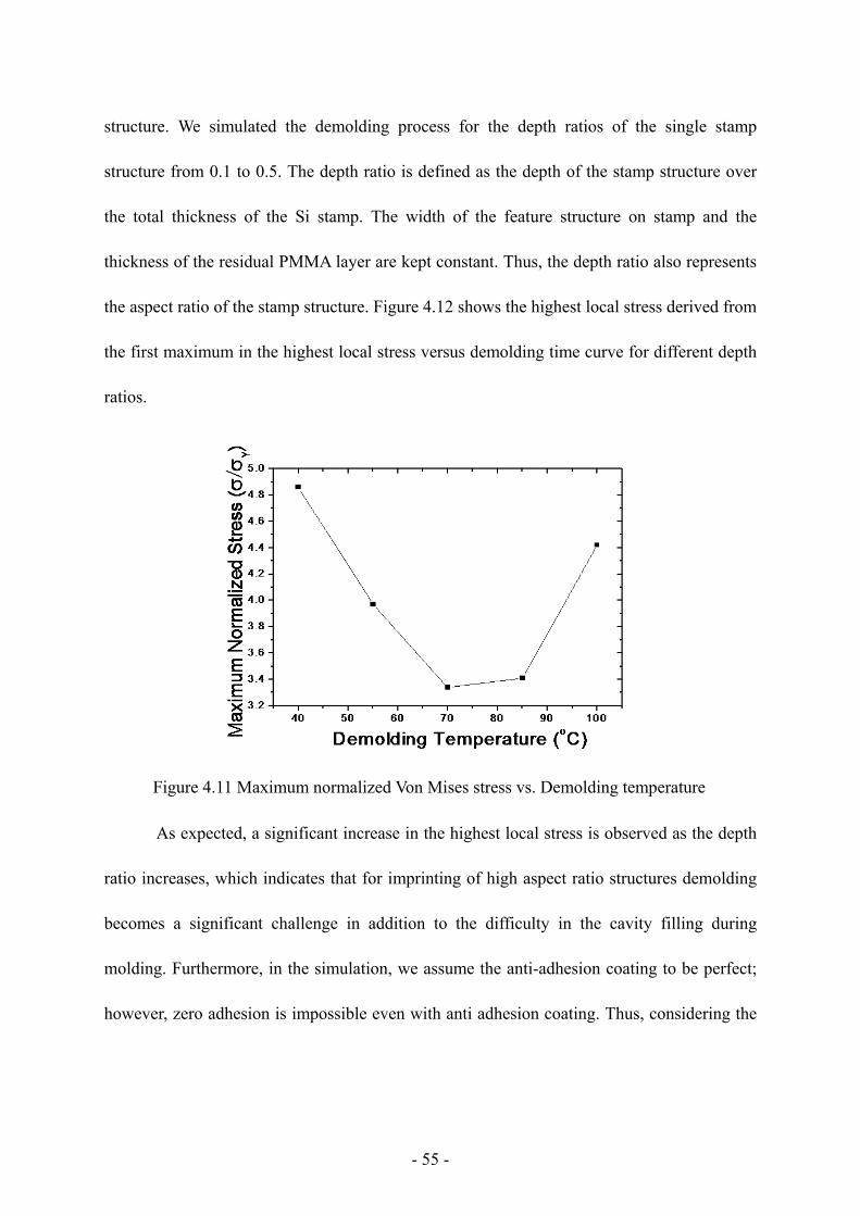
- 55 -
structure. We simulated the demolding process for the depth ratios of the single stamp
structure from 0.1 to 0.5. The depth ratio is defined as the depth of the stamp structure over
the total thickness of the Si stamp. The width of the feature structure on stamp and the
thickness of the residual PMMA layer are kept constant. Thus, the depth ratio also represents
the aspect ratio of the stamp structure. Figure 4.12 shows the highest local stress derived from
the first maximum in the highest local stress versus demolding time curve for different depth
ratios.
As expected, a significant increase in the highest local stress is observed as the depth
ratio increases, which indicates that for imprinting of high aspect ratio structures demolding
becomes a significant challenge in addition to the difficulty in the cavity filling during
molding. Furthermore, in the simulation, we assume the anti-adhesion coating to be perfect;
however, zero adhesion is impossible even with anti adhesion coating. Thus, considering the
Figure 4.11 Maximum normalized Von Mises stress vs. Demolding temperature

- 56 -
effect of adhesion force, high surface to volume ratio may bring additional difficulty in
fabrication of high aspect ratio structures.
4.4 Conclusions
The demolding process in thermal imprint lithography was studied in detail by the
FEM simulation based on the viscoelastic model of PMMA. We found two locations of stress
concentration in the PMMA layer during demolding: the corner of transition zone between
the replicated patterns to residual layer and the contact region between silicon stamp and
replicated patterns. As demolding proceeds, the highest local stress shows two maximums,
indicating that demolding failure can occur both at the beginning and the end of demolding. A
systematic parametric study has been performed on the demolding rate, demolding angle,
demolding temperature and the aspect ratio of the stamp structures. An accurate alignment in
the stamp displacement direction is critical to the success of demolding and there exists a
maximum allowed demolding angle leading to demolding without structural failure. Local
Figure 4.12 The highest local stress as a function of the depth ratio at the first maximum in the highest local stress versus demolding time curve for different depth ratios.
h
H
h/H=0.1 h/H=0.2
h/H=0.3 h/H=0.50.1 0.2 0.3 0.4 0.5
5.5x10⁷
6.0x10⁷
6.5x10⁷
7.0x10⁷
7.5x10⁷
8.0x10⁷
8.5x10⁷
9.0x10⁷
9.5x10⁷H
ighe
st L
ocal
Stre
ss (P
a)
Depth Ratio (h/H)

- 57 -
stress increases as demolding rate increases, particularly in non-normal demolding process.
Both simulation and experiment results show that the optimal demolding temperature in
given condition is around 70ºC, with both excellent overall pattern quality and satisfactory
local surface profile. Increase in the aspect ratio in the stamp structures leads to the increased
local stress during demolding, indicating the difficulty in fabrication of high aspect ratio
structures. In this paper, we only simulated simple structures such as a single symmetric
structure. However, the results indicate that, the ability of the FEM simulation for
complicated and actual structures will enable prediction of the demolding process as well as
determination of a range of process parameters which will allow for successful demolding
even at the stage of a process design in an economical and reliable way. This becomes more
important with the increasing requirement of high aspect ratio and complex structures.

- 58 -
Chapter 5 Experimental Study of Demolding Process in Thermal NIL
5.1 Introduction
In chapter 4, we simulated the demolding process in thermal imprint lithography via
finite element method and investigated the effects of several parameters, including demolding
rate, demolding temperature, demolding angle, and stamp geometry. From the simulation
results, rules of stress distribution and evolution were extracted and different parameters were
evaluated. To verify the reliability of simulation results, in this chapter, we studied demolding
in thermal imprint lithography via experimental approach. Since the only measurable
parameter to quantitatively characterize the mechanical resistance during demolding is
demolding force, which is defined as the force required releasing the stamp from the substrate.
We measured the demolding force using a temperature and rate controllable demolding unit,
which was modified from a standard mechanical tester. Particularly, we studied the effect of
demolding temperature. Even though the Si stamp/PMMA resist/Si substrate assembly used
in the experiments is not exactly identical to the 2D finite element model used for the
simulation in terms of the shape and size of the patterns, the experimental results show
satisfactory agreement with simulation result in general trends of stress evolution and
temperature dependence study.
5.2 Experiment Procedure
In this section, we introduce the entire procedure of the experimental study of
demolding force in sequence, including stamp fabrication, surface treatment, substrate
preparation, thermal imprinting, and demolding. Several critical techniques, such as
photolithography, silane coating and reactive ion etching are discussed in detail.
- 59 -
5.2.1 Stamp Fabrication
Stamp fabrication is the first step, and also one of the most important steps in thermal
imprint lithography. The quality of replicated patterns is directly determined by the quality of
stamp in terms of sidewall profile, aspect ratio, surface roughness and feature complexity. In
this section, we describe stamp fabrication procedure in sequence: photomask design, pattern
transfer by photolithography and reactive ion etching.
5.2.1.1 Photomask Design
A photomask is an opaque plate with holes or transparencies that allow light to shine
through in a defined pattern, which is widely used for selective patterning on silicon substrate
coated with photoresist in photolithography. Photomasks are typically transparent fused silica
blanks covered with a pattern defined with a chrome metal absorbing film. The patterns of
phtomask used in the experiment consist of line gratings and dot array, which are shown in
figure 5.1 and the detail information on the line width, dot size and period is given in table
5.1. The photomask design was then sent to a commercial company for the fabrication.
5.2.1.2 Photolithography
Photolithography, also known as optical lithography, is a widely used technique in
microfabrication to selectively remove parts of a thin resist film (or the bulk of a substrate). It
uses light to transfer a geometric pattern from a photomask to a light-sensitive chemical
(photoresist) on the substrate. A series of chemical treatments then engraves the exposure
pattern into the material underneath the photoresist.
Figure 5.2 presents schematics of the photolithography process. Test grade 4 inch
silicon wafer from Silicon Quest (Santa Clara, CA) weas firstly spin-coated with an adhesion

- 60 -
promoter, hexa-di-methyl-silazane (HDMS) at 3000 rpm for 60 s in order to promote the
adhesion between the photo-resist layer and the silicon substrate. After drying in air for 5 min
at room temperature, the HDMS coated wafer was further spin-coated with S1813 positive
photoresist from Shipley Company (Marlborough, MA) at 2000 rpm for 60 s and baked at 95°
C for 90 s; hence, a 2 μm thick resist S1813 layer forms on the wafer as verified by
profilometer measurements. Then, a UV exposure was performed on the coated silicon
Figure 5.1 AutoCAD pattern for the mask with line gratings and dot array
Table 5.1 Detail Information on pattern layout of photomask

- 61 -
substrate using a Quintel UL 7000-OBS aligner and DUV exposure station from Quintel
Corporation (Morgan Hill, CA), with the custom ordered photomask for a dosage of 70 mJ.
The exposed wafer was developed in MF 319 developer solution for 120 s. Two developer
trays were used to ensure better resist removal by reducing concentration changes of the
developer solution due to resist removal from the photomask; the first tray was used to
develop for about 40 s and the next tray was used for the remaining 80 s. The wafers were
washed in a DI water bath for 2 min and blow-dried with N2. Any residual resist layer in the
recessed area of the resist patterns was removed by etching with O2 plasma for about 10 s.
5.2.1.3 Reactive Ion Etching
Reactive ion etching (RIE) is an anisotropic etching technique widely used in
microfabrication. Chemically reactive plasma is used to remove materials deposited on
wafers or bulk silicon self. The plasma is generated under low vacuum by an electromagnetic
Figure 5.2 Schematic of photolithography

- 62 -
field and high-energy ions from the plasma attack the wafer surface.
A typical reactive ion etching (RIE) system consists of a cylindrical vacuum chamber,
with a wafer platter situated in the bottom portion of the chamber. The grounded wafer platter
is electrically isolated from the rest of the chamber. Gas enters through tiny inlets in the top
of the chamber, and exits to the vacuum pump system through the bottom. The types and
amount of gas used vary depending on the etching process; for instance, sulfur hexafluoride
is commonly used for etching silicon; oxygen is usually used to remove residual polymer.
Gas pressure is typically maintained in a range between a few millitorr and a few hundred
millitorr by adjusting gas flow rates and/or adjusting an exhaust orifice.
Plasma is initiated in the system by applying a strong RF (radio frequency)
electromagnetic field to the wafer platter. The field is typically set to a frequency of 13.56
megahertz, applied at a few hundred watts. The oscillating electric field ionizes the gas
molecules by stripping them of electrons, creating the plasma. In each cycle of the field, the
electrons are electrically accelerated up and down in the chamber, sometimes striking both
the upper wall of the chamber and the wafer platter. At the same time, the much more
massive ions move relatively little in response to the RF electric field. When electrons are
absorbed into the chamber walls they are simply fed out to ground and do not alter the
electronic state of the system. However, electrons absorbed into the wafer platter cause the
platter to build up charge due to its DC isolation. This charge build up develops a large
negative voltage on the platter, typically around a few hundred volts. The plasma itself
develops a slightly positive charge due to the higher concentration of positive ions compared
to free electrons. Because of the large voltage difference, positive ions tend to drift toward the

- 63 -
wafer platter, where they collide with the samples to be etched. The ions react chemically
with the materials on the surface of the samples, but can also knock off (sputter) some
material by transferring some of their kinetic energy. Due to the mostly vertical delivery of
reactive ions, reactive ion etching can produce very anisotropic etch profiles, which contrast
with the typically isotropic profiles of wet chemical etching.
For etching low aspect ratio structures in Si and for etching of PMMA for window
opening, a TECHNICS series 800 RIE machine located at the CBM2 facility on South
Campus of LSU was used. Two different gases, CF4 and SF6 are available for silicon etching.
SF6 etching is of high etching rate and usually creates an undercut for the etching profile,
which will lead to interlocking of resist material and thus demolding failures. The etching
rate of CF4 etching is much slower and produces sidewalls of highly tapered shape. Thus, we
combined these two gases together and tried to find an optimal condition for silicon etching,
which may give a preferred sidewall profile for NIL which is slightly tapered sidewalls.
Considering the much faster etching rate of SF6, we etched the silicon substrate by the
combination of the two gases with three different recipes: (CF4 90s + SF6 25s)×3, (CF4 150s
+ SF6 25s)×3 and (CF4 240s + SF6 25s)×3. The working power is 100 watts and the working
pressure is 250 millitorr. Figure 5.3 shows SEM imges for the silicon etching profile for
different recipes. The recipe of (CF4 240s + SF6 25s)×3 gives the best result with slightly
tapered sidewall that is preferred etching profile to be used as stamps for imprinting. The
depth of the structures for the stamp used for the demolding force experiments was 500 ~
1000 nm.

- 64 -
5.2.2 Surface Treatment – Anti Adhesion Coating
Despite significant advances in surface micromachining technology, strong adhesion
remains a key challenge, which limits the life time and reliability of MEMS devices. Local
defects, even structural collapse may occur during demolding as a result of strong adhesion,
particularly for the high aspect ratio structures with high surface to volume ratio. Strong
adhesion is generally caused by capillary, electrostatic and van der Waals forces, and in some
cases by ‘‘chemical’’ forces such as hydrogen bonding and solid bridging.
Self-assembled monolayer (SAM) coating has been demonstrated as an efficient way
in eliminating release stiction through minimization of the surface tension of stamp. In this
experiment, the SAM molecule used here is a fluorinated silane molecule 1H,1H,2H,2H-
Perfluorodecyltrichlorosilane (C10H4Cl3F17Si). This molecule consists of a head group with
three chlorosilanes and a fluorinated, long carbon chain (C10).
Upon deposition, the chlorinated silane groups in the molecule formed bonds with the
hydroxylated silicon surface with the presence of H2O on the surface, leaving volatile HCl
gas (Fig 5.4). In addition, cross-linking between silane groups in the neighboring molecules
also occurs, leading to a coating layer with high density. Those reactions between the head
group and the hydroxylated Si surface leave the fluorinated tail group at the surface side,
which renders the surface hydrophobic. As a result, the presence of a silane layer on Si lowers
the adhesion force between the polymer and the stamp with respect to an untreated stamp.
This helps ease demolding and produce better surface finish for the imprinted polymer. As
mentioned earlier, hydroxylation of the Si surface is a prerequisite for such reactions to occur,
which was achieved by treating Si surfaces with O2 plasma shortly before the silane coating

- 65 -
operation.
Prior to silane coating, silicon stamps were cleaned sequentially with acetone,
isopropanol, and distilled water and then exposed to O2 plasma at 150 watts and 250 millitorr
for about 10 s in order to produce the hydroxylated Si surface. The stamp is blow-cleaned by
Figure 5.3 Silicon etching profile for different recipes (a) (CF4 90s + SF6 25s)×3; (b) (CF4 150s + SF6 25s)×3; (c) (CF4 240s + SF6 25s)×3

- 66 -
compressed N2, then loaded into the CVD chamber. The chamber is evacuated to the base
pressure of 6×10⁻² torr. After shutting down the valve to the pump, the valve to the ampule
filled with the fluorinated silane is opened and the sample is exposed to the evaporated silane
molecules, which diffuses from the ampule to the chamber, for 10 min. After silane
deposition, the valve to the ampule is closed and the chamber is again evacuated to the base
pressure before venting the chamber with Argon gas. After removing the sample, the chamber
is subsequently cleaned with acetone and pumped again to the base pressure so that the
system is kept under vacuum until the next use.
The quality of anti-adhesion coating was evaluated by contact angle measurements
because the surface energy of a surface is related to the contact angle by Young’s Equation.
Figure 5.5 shows the variation of water contact angles of a silicon wafer surface before and
after silane coating. It can be seen that the water contact angle significantly increases from
Figure 5.4 A schematic of silane coating on silicon surface

- 67 -
39° to 107°, indicating an increased hydrophobicity of the silicon surface.
Since only a monolayer of silane molecules needs to be formed on the silicon surface,
excessive coating time will not enhance the coating quality and even make it worse. Figure
5.6 shows the contact angle as a function of coating time. Usually, 5 - 10min is a proper
deposition time for silane coating.
5.2.3 Thermal Imprint Lithography
The procedure of thermal imprint lithography consists of three steps in sequence:
molding (including preheating), cooling and demolding, which altogether determine the
replication fidelity and the mechanical stability of the patterns. During the molding step, a
silicon stamp with desired structures is pressed into a substrate coated with a thin polymer
resist. After conformal molding, the stamp/substrate assembly is cooled down to below the
glass transition temperature (Tg) of the resist while pressure is held constant. Finally, the
pressure is released and the stamp is separated from the substrate during demolding. The
schematic of thermal imprint lithography has already been shown in figure 2.1
Figure 5.5 Water contact angle on a silicon wafer before and after silane coating

- 68 -
5.2.3.1 Spin Coating
Prior to spin coating, a silicon wafer was preheated at 95ºC for 5 min to dehydrate the
Si surface. An excess amount of a PMMA solution was placed on the substrate by syringe
through a filter in order to remove any dust particles and air bubbles. Then, the substrate was
rotated at a certain angular velocity to homogeneously coat the PMMA over the silicon
surface. The angular velocity of rotation is determined by several factors, including the
required film thickness, the concentration of PMMA solution and the molecule weight of
solute PMMA. For example, to deposit PMMA film of 10 μm, we spin coated 25% weight
percentage, 25,000 molecule weight PMMA solution on silicon wafer at 1000 rpm for 60s.
After spin coating, the sample was soft baked for another 5 min at 95ºC.
5.2.3.2 Thermal Imprinting
Commercial Obducat nanoimprint system was employed in imprinting experiments,
which is shown in figure 5.7. Imprinting pressure, temperature and time were set to be 40 bar,
175ºC and 30min, respectively. A piece of a rubber sheet was placed on top of the silicon
stamp to ensure homogenous distribution of pressure. As shown in figure 5.8, imprinted
Figure 5.6 Water contact angle on silicon wafer as a function of coating time

- 69 -
PMMA patterns exhibited satisfactory overall pattern quality and local contrast. All the
operations were performed in a 1000× modulus cleanroom (Figure 5.9).
5.2.4 Demolding Experiment
Demolding is a process to overcome all level chemical and mechanical interactions
between silicon stamp and PMMA resist, formed by the history of molding and cooling. For
the laboratory scale imprinting of micro- and nanostructures, demolding is performed
Figure 5.8 Imprinted PMMA patterns of line gratings with 9μm width and 18μm period
Figure 5.7 Obducat 6 inch nanoimprit system

- 70 -
manually using a sharp razor blade. There are several inherent disadvantages for this
manually demolding method. First, it is difficult to control the demolding rate and structural
damages may occur as a result of the impact load. Second, the stamp is not normally
separated from the substrate and non-zero demolding angle would increase concentrated local
stress. Third, since the demolding is performed manually, high temperature demolding
(~100ºC) is a challenge and accurate temperature control is also difficult to be realized. In
order to overcome all the difficulties mentioned above, an automatic demolding unit is built
based on a standard mechanical tester from MTS Company.
5.2.4.1 Standard Mechanical Tester
Figure 5.10 shows the main frame of standard mechanical tester MTS Insight 5,
which is used to acquire the force-displacement relationship during demolding. Demolding
rate was controlled by accompanied software Testwork 4. The minimum test speed is 0.001
mm/min and the speed accuracy is ±0.05% of the full speed. The position resolution is
0.001mm. Demolding force is detected by the load cell of 5 kN capacity and the accuracy of
Figure 5.9 1000× class modulus cleanroom

- 71 -
force measurement is ±0.03%.
5.2.4.2 Fabrication of Vacuum Chuck
The fixture to hold the imprinted silicon stamp/PMMA resist/silicon substrate
assembly during demolding is another important component in the system. There are several
requirements that need to be considered in the design and building of the fixture. First, the
low toughness silicon stamp/substrate should not be broken in test. Since silicon is only ~500
μm thick, it is difficult to fix the thin wafer with metallic clamps. In addition, Si is a very
brittle material and thus, metallic clamps could be the point of stress concentration. Second,
the position of Si stamp and substrate must be fixed to ensure the normal demolding. Since
the thickness of silicon wafer is very thin (~500μm), it is extremely difficult to fix the silicon
stamp and substrate firmly from sides. Third, to ensure accurate force measurement, no soft
Figure 5.10 Automatic demolding unit based on a standard mechanical tester

- 72 -
material which may serve as a damping layer should be added in. Fourth, the force should be
applied uniformly on the whole area of stamp. Fifth, it should be easy to separate the sample
from adapter, without any contamination, both for sample and fixtures. As a result, glue
cannot be used to sample to the main frame of material tester.
In order to satisfy all the requirements mentioned above, a brass vacuum chuck was
built to hold the Si stamp/PMMA resist/Si substrate assembly. Figure 5.11(a) shows the side
view of vacuum chuck and figure 5.11(b) is the top view of AutoCAD design of the vacuum
chuck.
The theoretical maximum holding force can be calculated based on the groove area:
52 2
max 0 2 2 11
F ( ) (1 5 ) ( )V V n nn
P P S e P r rπ −=
= − × = − × × −∑
10
1(1 5 ) 282.6 0.002826 ( )V n V
ne P d r P Nπ
=
= − × × ≈ − ×∑ (Equation 5.1)
where P0 refers to one atmosphere; PV refers to the vacuum pressure inside the chuck; rn
refers to the radius of the nth groove.
Figure 5.11 (a) Side view of the brass vacuum chuck and (b) Top view of AutoCAD design of vacuum chuck
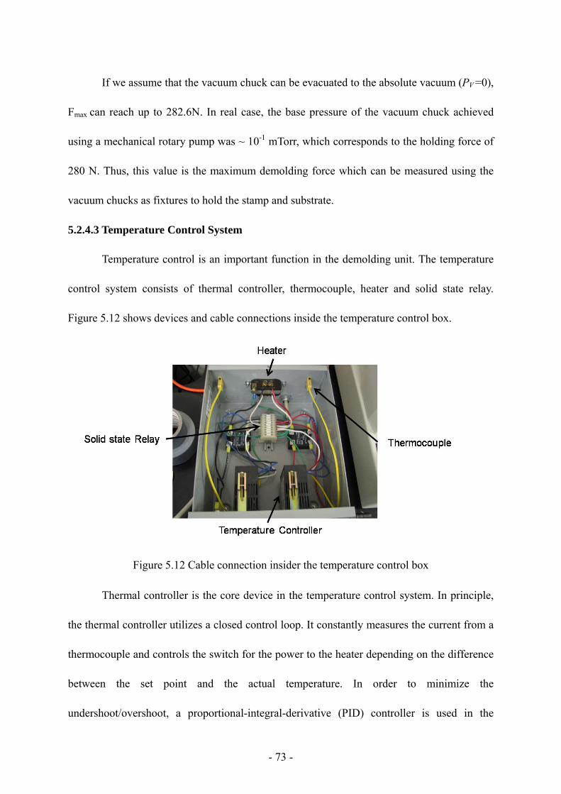
- 73 -
If we assume that the vacuum chuck can be evacuated to the absolute vacuum (PV =0),
Fmax can reach up to 282.6N. In real case, the base pressure of the vacuum chuck achieved
using a mechanical rotary pump was ~ 10-1 mTorr, which corresponds to the holding force of
280 N. Thus, this value is the maximum demolding force which can be measured using the
vacuum chucks as fixtures to hold the stamp and substrate.
5.2.4.3 Temperature Control System
Temperature control is an important function in the demolding unit. The temperature
control system consists of thermal controller, thermocouple, heater and solid state relay.
Figure 5.12 shows devices and cable connections inside the temperature control box.
Thermal controller is the core device in the temperature control system. In principle,
the thermal controller utilizes a closed control loop. It constantly measures the current from a
thermocouple and controls the switch for the power to the heater depending on the difference
between the set point and the actual temperature. In order to minimize the
undershoot/overshoot, a proportional-integral-derivative (PID) controller is used in the
Figure 5.12 Cable connection insider the temperature control box

experim
variable
adjust th
derivati
integral
reaction
constan
process
oscillati
range
our ex
type t
Alumi
ment. A PID
e and a desi
he process a
ive values.
l determine
n based on
nts in the PI
s requireme
ion. Figure
Thermoco
of tempera
xperiment, K
thermocoup
inum Alloy)
Solid state
D controlle
ired setpoin
accordingly
The propo
es the react
the rate b
ID controlle
ents includ
5.13 shows
ouple is a w
atures, offer
K type therm
ple is made
) and availa
relay (SSR
Figure
er attempts
nt by calcula
y, based upo
ortional valu
tion based
by which th
er algorithm
ing error r
s a blog diag
widely used
ring excelle
mocouple is
e of Chrom
able from -2
R) is an ele
5.13 A bloc
- 74 -
to correct
ating and th
on three par
ue determin
on recent e
he error ha
m the PID c
responsiven
gram of a P
type of tem
ent comprom
used to be
mel (Nicke
200ºC to 120
ectronic sw
ck diagram
the error
hen outputti
ameters, the
nes the reac
errors and
as been cha
can provide
ness, oversh
ID controlle
mperature se
mise of cos
compatible
el-Chromium
00ºC with a
witch. Unlik
of a PID co
between a
ing a correc
e proportion
ction to the
the derivat
anging. By
e individual
hoot of se
er.
ensor and c
st, accuracy
e with the th
m Alloy) /
accuracy of
ke an electr
ontroller
measured
ctive action
nal, the inte
e current er
tive determ
"tuning" th
lized contro
etpoint and
can measure
y and reliab
hermal contr
/ Alumel
±2.2ºC.
romechanic
process
that can
egral and
rror, the
ines the
he three
ol of the
system
e a wide
bility. In
roller. K
(Nickel-
al relay,

- 75 -
SSR contains no moving parts. The types of SSR include photo-coupled SSR, transformer-
coupled SSR, and hybrid SSR. A photo-coupled solid state relay is controlled by a low
voltage signal which is isolated optically from the load. The control signal in a photo-coupled
SSR typically energizes an LED which activates a photo-sensitive diode. The diode turns on a
back-to-back thyristor, silicon controlled rectifier, or MOSFET transistor to switch the load.
Heater is the output element in the system. A group of electric-thermal resistances are
embedded in a brass block with excellent thermal conductivity. The heater is activated by DC
power voltage and cooled off by air convection. The system can be heated up at 5ºC/min.
The working mechanism of the temperature control system is simple. The
thermocouple is placed into a hole built in a vacuum chuck to detect the surface temperature.
The temperature reading is then sent to the temperature controller as an input signal. If the
detected temperature is lower than the set point, output signal will active the heater to heat up.
As soon as the detected temperature reaches the set point, the solid state relay becomes active
and the temperature is maintained at the setpoint.
5.3 Results and Discussion
In this section, we present results from demolding force measurements performed
with the modified mechanical tester and scanning electron microscope (SEM) images of the
imprinted PMMA patterns. After reproducibility testing, systematic measurements were done
to investigate influence of demolding temperatures. Finally, we discuss the experimental
results and compare with pervious simulation results.
5.3.1 General Force-Displacement Response during Demolding
Demolding failures are determined by the value of local stress in resist with respect to
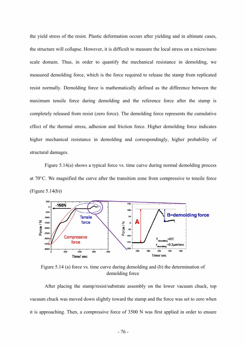
- 76 -
the yield stress of the resist. Plastic deformation occurs after yielding and in ultimate cases,
the structure will collapse. However, it is difficult to measure the local stress on a micro/nano
scale domain. Thus, in order to quantify the mechanical resistance in demolding, we
measured demolding force, which is the force required to release the stamp from replicated
resist normally. Demolding force is mathematically defined as the difference between the
maximum tensile force during demolding and the reference force after the stamp is
completely released from resist (zero force). The demolding force represents the cumulative
effect of the thermal stress, adhesion and friction force. Higher demolding force indicates
higher mechanical resistance in demolding and correspondingly, higher probability of
structural damages.
Figure 5.14(a) shows a typical force vs. time curve during normal demolding process
at 70°C. We magnified the curve after the transition zone from compressive to tensile force
(Figure 5.14(b))
After placing the stamp/resist/substrate assembly on the lower vacuum chuck, top
vacuum chuck was moved down slightly toward the stamp and the force was set to zero when
it is approaching. Then, a compressive force of 3500 N was first applied in order to ensure
Figure 5.14 (a) force vs. time curve during demolding and (b) the determination of demolding force

- 77 -
that the top vacuum chuck is in hard contact with the backside of silicon stamp so that no
leakage occurs at the interface. Note that the negative sign of force corresponds to a
compressive force. After that, the top vacuum chuck was moved up at a velocity of 0.03 μm/s.
As demolding proceeds, the compressive force was released and the slope of the curve in
compressive region was the global stiffness of the assembled parts along the displacement
direction. The nonlinearity of the measured force-time curve was due to some flexible parts
(most probably the composite plates for thermal insulation) and slight misalignment between
the two vacuum chucks. When the compressive force reached approximately -150 N, the
force-time curve entered a flat regime in which the contact force is constant while demolding
proceeds. We believed that it was the transition zone from compressive to tensile state.
Interestingly, the compressive to tensile transition did not occur at zero force, but -150 N. The
difference was considered to be an additional force required to overcome the bending of
substrate. After compressive to tensile transition, the tensile force kept increasing and the
stamp/resist/substrate assembly was pulled from both sides. Then, the force value reached a
maximum and finally dropped back to zero force after the stamp was completely released
from the resist. The demolding force is defined as the difference between the peak value of
tensile force and the force after the stamp is totally demolded, as shown in the plot.
For each demolding condition, at least four effective measurements were performed.
For the case that significant defects are observed in the molded structure after demolding, the
measured data were discarded because the measured force then cannot account for the actual
demolding force. Figure 5.15 shows force-time curves for a sequence of identical
measurements for demolding at room temperature. The average demolding force is 77.1 N

- 78 -
and the standard deviation amounts to 15 N.
5.3.2 Influence of Demolding Temperature
Temperature is one of the most important parameters for demolding in thermal
imprint lithography not only because the flow of polymer resist in molding process depends
on temperature, but also because the thermal stress, friction, adhesion and mechanical
strength of resist are temperature-dependent. In principle, the thermal stress generated during
cooling for elastic materials is linearly proportional to the temperature difference between the
molding and demolding, assuming thermal expansion coefficient to be constant; the adhesion
is stronger and friction coefficient is also higher at lower temperature, because the chemical
interactions are more stable [Hammerschmidt et al., 1999]; the mechanical strength of
PMMA is monotonously decrease function of temperature. As a result, an optimal demolding
temperature may be determined by consideration of all aspects of material properties and
process conditions
In this experiment, we measured the contact force during demolding with identical
Figure 5.15 4 measurements of force-displacement curve at 25 ºC and 0.3 µm/s
260 280 300 320 340-200
-150
-100
-50
0
50
100
150
Forc
e / N
Time/ sec

- 79 -
stamp and substrate at three different temperatures (25°C, 70°C and 100°C) and repeated at
least four times at each temperature.
Figure 5.16 (a) shows the force-time curve at three different temperatures. The
general trends of the force-time curve are similar at different temperatures, which consists of
four regions: compressive force (F < 150 N); compressive to tensile transition (F = 150N);
tensile force (F > 150N) and zero force status after releasing. However, the demolding force
values show great variation. Figure 5.16(b) plots the demolding force obtained from the
force-time curves at three different demolding temperatures, which clearly indicates that there
the best demolding temperature among three tested temperatures, is 70°C.
5.3.3 Inspection of Imprinted PMMA Patterns
To understand the temperature effect, we also observed the replicated PMMA patterns
demolded at different temperatures by scanning electronic microscope (SEM). Figure 5.17
shows the replicated PMMA patterns of 5 μm line width, 10 μm period and 10 μm depth. It
should be noted that the stamp used for the demolding force measurements was 4 inch wafer
and has low aspect ratio patterns with ~ 50 nm thickness because the maximum demolding
Figure 5.16 (a) Contact force vs. extension at different demolding temperature and (b) demolding force vs. demolding temperature

- 80 -
force that can be measured using the designed vacuum chucks was 282.6 N. For SEM
inspection, high aspect ratio patterns were used for a better observation of demolding failure
that might occur at different demolding conditions.
At a demolding temperature of 25°C, large portion of imprinted PMMA patterns were
ripped off due to high thermal stress and adhesion, even though the survived structures show
excellent surface roughness and sharp sidewall; at 100°C, most of the transferred patterns
survived after demolding, however, large local plastic deformation occurred at top surface,
the sidewalls as well as the bottom trenches of imprinted patterns due to low mechanical
strength of PMMA at elevated temperature. When the demolding was performed at 70°C, the
local plastic deformation in the imprinted PMMA patterns is significantly reduced and the
global pattern quality is satisfactory, furthermore, the inspection corroborates the demolding
force measurement results in which the optimal demolding temperature was found to be
70°C.
5.3.4 Comparison with Demolding Simulation
Both the inspection of the imprinted PMMA patterns and the measurement of
demolding force showed that 70ºC is the optimal demolding temperature with the stamp
design, resist and process conditions used in the experiment. Demolding at high temperature
will not result in large area damages in patterns such as ripping, however, local distortion and
warpage occur, thus reduce the accuracy of pattern transformation; on the other hand, low
demolding temperature shows excellent profile of replicated PMMA patterns, but, large
portion of patterns are ripped off due to extremely high residual stress. The demolding force
measurement also shows lower demolding force at 70ºC, which implies that the demolding is
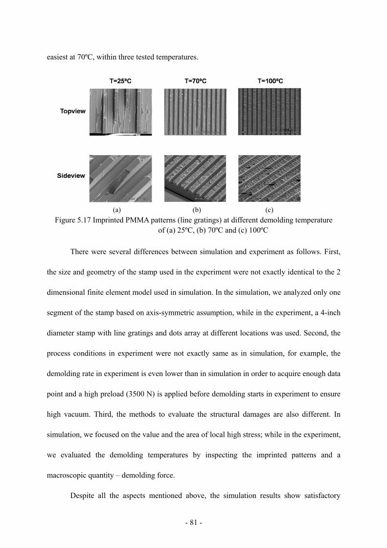
- 81 -
easiest at 70ºC, within three tested temperatures.
There were several differences between simulation and experiment as follows. First,
the size and geometry of the stamp used in the experiment were not exactly identical to the 2
dimensional finite element model used in simulation. In the simulation, we analyzed only one
segment of the stamp based on axis-symmetric assumption, while in the experiment, a 4-inch
diameter stamp with line gratings and dots array at different locations was used. Second, the
process conditions in experiment were not exactly same as in simulation, for example, the
demolding rate in experiment is even lower than in simulation in order to acquire enough data
point and a high preload (3500 N) is applied before demolding starts in experiment to ensure
high vacuum. Third, the methods to evaluate the structural damages are also different. In
simulation, we focused on the value and the area of local high stress; while in the experiment,
we evaluated the demolding temperatures by inspecting the imprinted patterns and a
macroscopic quantity – demolding force.
Despite all the aspects mentioned above, the simulation results show satisfactory
(a) (b) (c) Figure 5.17 Imprinted PMMA patterns (line gratings) at different demolding temperature
of (a) 25ºC, (b) 70ºC and (c) 100ºC

- 82 -
agreement with the experiment inspection and measurements with regard to demolding
temperature. Both confirmed that an optimal demolding temperature lies between the high
and low temperature, which implies a balance between the absolute value of residual stress
and mechanical strength of the material.

- 83 -
Chapter 6 FEM Simulation for UV Imprinting
6.1 Introduction
UV nanoimprint lithography (UV-NIL), also known as step and flash imprint
lithography, is an important variant of nanoimprint lithography developed by Wilson’s group
1997. Figure 6.1 shows schematic of the UV-NIL process. First, an organic transfer layer is
spin coated on a silicon substrate; then, a transparent stamp with desired micro/nanostructures
is closely aligned over the coated substrate; once in proximity, a low viscous solution of
photopolymerizable resin is dispensed into the gap between the substrate and the stamp; the
microcavities on the stamp is filled by the resin as a result of capillary action; once the stamp
cavities are fully filled by the resin, the whole assembly is exposed to UV light and the resin
is solidified by the cross-linking of resin; finally, the stamp is separated from the substrate
and usually, the process is followed by transfer layer etching by O2 plasma and barrier
striping.
Compare with thermal NIL, UV-NIL has several critical advantages: First, in thermal
NIL, the polymer resist is heated above its glass transition temperature in molding, as a result,
high thermal stress is formed in the polymer resist as cooling down to demolding temperature.
Furthermore, the heating and cooling processes cost longer time other than molding self;
however, in UV-NIL, the photolymerizable resin is solidified by UV irradiation, the intrinsic
stress due to the crosslinking of photolymerizable resin is much lower than the thermal stress
in thermal NIL and also, cycle time is greatly shorten since no heating and cooling processes
are needed. Second, in thermal NIL, the polymer flow is driven by high external pressure,
thus, for stamps with large depressed area and high aspect ratio structures, incomplete filling

- 84 -
of the cavities may occur; by the way, the stamp may be bended or even damaged during
imprinting; however, in UV-NIL, the flow behavior of photolymerizable resin is driven by the
capillary force, thus, it is more suitable for large area and high aspect ratio imprinting because
the filling process in UV-NIL is much easier than thermal NIL; moreover, since no high
pressure is applied, the lifetime of stamp is prolonged and flow stress is lower. Third, due to
high pressure and adhesion force between the stamp and polymer resist, high demolding force
is required to release the stamp from imprinted patterns in thermal NIL; however, in UV-NIL,
no high demolding force is required.
In this chapter, we simulated the solidification process in UV-NIL using commercial
FEM software, ANSYS 10.0. The distribution of Von Mises stress was studied and compared
with thermal NIL. It was found that for the identical model the solidification process in UN-
Figure 6.1 Schematic of step and flash imprint lithography (UV imprint lithography)

- 85 -
NIL induces much lower stress than the residual thermal stress in thermal NIL.
6.2 Volumetric and Mechanical Properties
The solidification of the photopolymerizable resin with UV exposure occurs via
cross-linking between the photopolymer precursors and is accompanied by volumetric
shrinkage. During the cross-linking reaction, interaction potential between photopolymer
precursors changes from Van der Waals force to covalent bonding. The average distance
between the molecules decreases and leads to volumetric contraction. Volumetric shrinkage
usually depends on the composition of the precursor resin, time and intensity of UV
irradiation. We simulated the solidification process with different volumetric shrinkage from
(0.3% to 3%) which occurs during UV NIL and found that the local high stress is linearly
proportional to volumetric shrinkage.
Mechanical properties including Young’s modulus and Poisson’s ratio also depend on
exposure conditions and material composition. Even though many UV-curable resins are
commercially available, there is no representative resin like PMMA or PC used in thermal
NIL. Thus, we took in our simulation the UV-curable resin used in the work of Mary B.
Chan-Park et al. and used the materials properties thereof. The Young’s modulus is 4 MPa
and the Poisson’s ratio is 0.3 [Park et al., 2005].
6.3 Finite Element Method Model and Preliminary Theoretical Analysis
Since ANSYS software is not able to simulate the UV irradiation and solidification
process directly, isotropic equivalent thermal strain is applied on the resin based on the
volumetric shrinkage. 4-nodal linear structural element PLANE42 is applied for all the
components including stamp, photoresist and substrate, and a contact pair TARGET169-

- 86 -
CONTACT172 is created at the interface between stamp and UV-curable resin.
2D FEM model (Figure 6.2) was created based on the plane stress assumption. The
bottom surface of substrate is confined and symmetric boundary condition is applied on the
centerline. A glued interface is defined between Si substrate and the UV-curable resin, and a
slip allowed interface is defined between stamp and the resin. The top surface of stamp was
confined.
To calculate the equivlant thermal strain, we assume that the volumetric shrinkage is
homogeneous and isotropic in the layer of the UV-resin, as shown in figure 6.3. The linear
contraction can be related to the volumetric shrinkage by the following equation:
3
X Y VX Y VΔ Δ Δ
= = (Equation 6.1)
Thus, the thermal stress on X and Y direction can be simply expressed as:
3XE X E V
X Vσ Δ Δ
= = ;3Y
E Y E VY V
σ Δ Δ= = (Equation 6.2)
Due to the plane stress assumption, we have:
0Zσ = (Equation 6.3)
Figure 6.2 2 D FEM model of stamp/photoresist/substrate assembly used in simulation

- 87 -
Thus, Von Mises stress can be calculated:
2 2 2( ) ( ) ( )2 3
X Y X Z Y ZX Y
E VV
σ σ σ σ σ σ σ σ− + − + − Δ= = = (Equation 6.5)
From equation 6.5, the local stress is proportional to the volumetric shrinkage. Thus, a
proper combination of process parameters, thus, it is crucial to minimize the volumetric
shrinkage of the resin in solidification.
6.4 Simulation Results of Solidification in UV Imprint
To study the local stress distribution in UV-curable resist after solidifcation, we
simulated the solidification process with different shrinkage ratio, from 0.3% to 3%. Figure
6.4 shows the distribution of Von Mises stress in resist domain after solidification. The
highest local stress increases linearly as volumetric shrinkage increases. At the lowest
volumetric shrinkage of 0.4%, the stress distribution is low and almost uniform over the
whole area; while at the highest volumetric shrinkage of 3%, the highest local stress is
Figure 6.3 Schematic of volume shrinkage during solidification

- 88 -
concentrated at the corner of transition zone between replicated patterns and residual layer,
similar to the stress distribution in the thermal NIL.
Figure 6.4 Von Mises stress distribution in UV resist after solidification for different volumetric shrinkage (mark the highest local stress in each figure)
Figure 6.5 the highest local stress as a function of volumetric shrinkage.
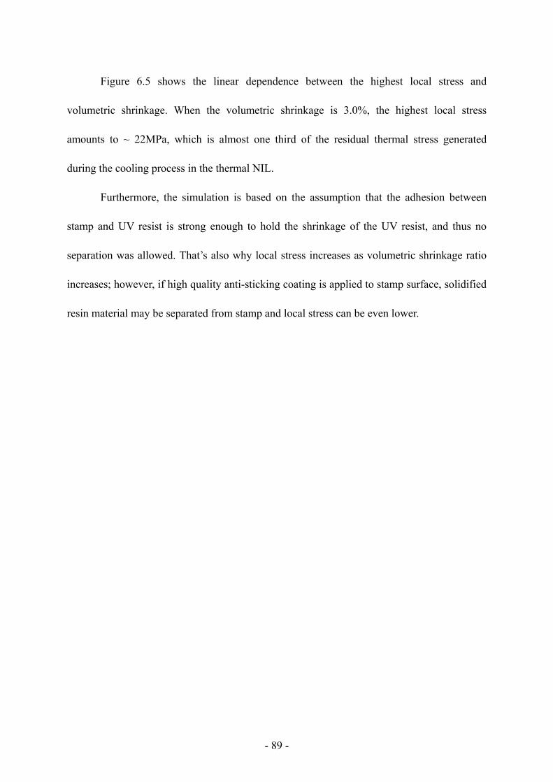
- 89 -
Figure 6.5 shows the linear dependence between the highest local stress and
volumetric shrinkage. When the volumetric shrinkage is 3.0%, the highest local stress
amounts to ~ 22MPa, which is almost one third of the residual thermal stress generated
during the cooling process in the thermal NIL.
Furthermore, the simulation is based on the assumption that the adhesion between
stamp and UV resist is strong enough to hold the shrinkage of the UV resist, and thus no
separation was allowed. That’s also why local stress increases as volumetric shrinkage ratio
increases; however, if high quality anti-sticking coating is applied to stamp surface, solidified
resin material may be separated from stamp and local stress can be even lower.

- 90 -
Chapter 7 Demolding Simulation for Injection Molding
7.1 Introduction
With the rapid advance of micro and nanotechnologies, high quality, low cost and
high throughput fabrication methods of MEMS devices are of crucial importance. Injection
molding, a well established technique in macroscopic production of polymer parts in industry
for decades, has been accommodated as a microfabrication technique by minimizing the
structure size on mold insert to micro scale [Su et al., 2004].
Similar to the thermal imprint lithography, the injection molding process consists of
three steps in sequence: injection (molding), cooling and ejection (demolding). First, a melted
polymer is fed by a screw into the mold block through a nozzle; then it fills into microcavities
of the mold insert at an injection molding temperature which is well above the glass transition
temperature of the polymer. For many injection molding processes, additional compression is
Figure 7.1 Schematic and equipment of injection molding [Courtesy of B. You et al]

- 91 -
applied to the mold block in addition to the pressure applied by the screw. The system is then
cooled down to an ejection temperature and the polymer filled into the microcavities is
solidified. Finally, the molded polymer part is separated from the mold insert at the ejection
temperature. There are significant differences in terms of physical process between injection
molding and thermal imprint lithography – for injection molding, the polymer melt at the
sprue is frozen first during cooling and after the polymer at the sprue is frozen, pressure on
molded part is released, thus, molded part can shrink freely.
Compared with other molding techniques such as thermal imprint lithography (hot
embossing), thermal forming and casting, injection molding has much shorter cycle time.
Thus, it is the preferred process for the cost-effective mass production of polymeric products
at the industrial level.
When injection molding is used for producing micro- and nanoscale patterns, the
increased surface-to-volume ratio significantly affects the flow behavior of the polymers.
Significant researches have been done in the study of mechanical and thermal behavior of the
melted polymer during injection [Hung et al., 2001; Yu et al., 2002; Ruprecht et al., 2002;
Despa et al., 1999]. Both numerical simulation and experimental measurement showed that
proper combinations of injection parameters, like the mold cavity temperature and injection
speed and injection pressure ensure the perfect dimension accuracy of pattern replication.
However, the study of cooling and ejection (demolding) process in injection molding is still
lacking, even though most of structural failures of molded polymer parts occur during these
steps. High local stress is generated in both the mold insert and molded polymer parts mainly
due to three factors: the first is the thermal stress formed during cooling as a result of the

- 92 -
mismatch of thermal expansion coefficients between the mold insert and the molded polymer
part; the second is the adhesion between the mold insert surface and molded part, from
chemical bonding, electrostatic interaction or mechanical interlock and it becomes significant
when the structure scales down or anti-sticking coating of the mold insert surface is not
perfect; the third is friction force between mold insert and molded part when relative sliding
occurs, which is simply assumed to be linearly proportional to the normal force due to the
thermal stress and the adhesion force. The proportionality constant is known as friction
coefficient. In order to minimize the thermal and adhesion induced stress, thus to ensure the
success of pattern replication, in-depth understanding of the mechanical response of molded
polymer part during cooling and demolding is imperative.
Recently, several groups have focused on the study of polymer mechanical behavior
during cooling and demolding [Fu et al., 2006; Worgull et al., 2006]. Fu et al. analyzed the
stress evolution during the ejection process of injection molding and concluded that the
microstructures at the edge of mold insert is exposed to the highest stress while inside
structures are protected [Fu et al., 2006]. Based on isotropic shrinkage assumption, they
predicted that a critical temperature exists, below which there is no surface contact between
mold insert and resist and thus demolding force is zero. However, the isotropic shrinkage
assumption used in their study is questionable, since only the thermal shrinkage towards the
local center of a certain micropost is considered while the global thermal shrinkage towards
the centerline of the whole mold insert/molded part was not taken into account. This will lead
to a significant error in predicting the stress and deformation behavior during demolding,
particularly for those structures far from the global centerline. Worgull et al. simulated the

- 93 -
cooling process in hot embossing and studied the location dependence of local stress
[Worgull et al., 2006]. Based on simulation results, they proposed a method of building
additional structures around the active pattern area to protect the active patterns from the high
stress concentration. However, the demolding process during hot embossing is different from
that for injection molding as described above. In this chapter, we extend the finite element
method (FEM) simulation to the demolding process for injection molding in order to achieve
a better understanding of the stress distribution and evolution, and deformation behavior of
molded polymer parts. Simulation results show that the microstructures at the edge of mold
insert is exposed to the highest shear stress resulting in a visible distortion in the molded part.
The microstructures inside are protected from high stress and no visible deformation was
observed. We also study the influence of the friction coefficient and geometries of the
microstructures in the mold insert. We find that the local maximum stress in the molded part
can be reduced up to 25% by modifying sharp corners of the microstructures in the mold
insert to have a draft angle.
7.2 Simulation Methodology and Results
7.2.1 2 Dimensional FEM Model
Figure 7.2 shows the 2-D finite element method (FEM) model and the boundary
conditions used in the simulation. The materials for the mold insert and the substrate were
brass and polycarbonate (PC) sheet, respectively. The brass mold insert contains three
identical recessed structures located at 100, 200 and 300 mm from the centerline (symmetric
boundary). The width and depth of the recessed structure are both 400 μm. The plane stress
assumption was made to simplify the simulation. This can be justified because there is little

- 94 -
deformation of the molded part in the vertical direction during the whole processes of cooling
and demolding. Vertical displacement was confined at both the top surface of the brass mold
insert and the bottom surface of the molded PC part. A symmetric boundary condition was
applied on the centerline. 4-nodal linear structural element PLANE42 was applied on both
brass mold insert and molded PC pattern, with gradually decreased element size from 50 μm
for areas of low and uniform stress distribution to 12.5 μm for sharp corners and interfaces
where high stress is concentrated. A standard contact pair of TARGET169-CONTACT172
was created on the interface between the mold insert and the molded PC part. Sliding and
separation were allowed at the interface.
7.2.2 Mesh Sensitivity
To ensure the reliability of simulation results, it is necessary to verify the convergence
of the simulation; in other word, the results are independent on the mesh size. To prove that,
we meshed the model with elements of different sizes while the element size ratio between
different region kept identical. Simulation was repeated under identical conditions (material
properties, contact alogrithm, load step). As shown in Figure 7.3, after cooling, shear stress at
Figure 7.2 2 dimensional FEM model for cooling and demolding simulation

- 95 -
the interface near the corner area converges to a certain value while the mesh density
increases. This indicates that the finite element analysis is mathematically reliable.
7.2.3 Process Assumptions
To simplify the finite element analysis without losing rationality and generality,
several assumptions were introduced.
First, the mechanical response of both brass mold insert and PC substrate at simulated
scale (microscale) is governed by equations of the continuum mechanics.
Second, microcavities in the brass mold insert are completely filled with the PC melt
at the molding temperature of 300 °C. Su et al. showed by simulation as well as experiment,
that at 300 °C and 50MPa injection pressure, the depth to opening ratio approaches 0.707,
which means the optimal filling [Su et al., 2004]
Third, the stress in the PC melt during the injection process is neglected. This
assumption can be justified by results of the temperature-dependent residual stress
Figure 7.3 Shear stress versus the path indicated in the inset for different numbers of mesh in order to verify the mesh Convergence

- 96 -
measurement at the polymer-metal interface [Wang et al., 2001]. Since the injection
temperature is well above the glass transition temperature of given polymer, the flow stress is
much less than the thermal stress generated during cooling and the shear stress at the
interface due to friction during demolding.
Fourth, there is no heat transfer between different components during cooling and the
whole system is cooled down at an identical cooling rate.
Fifth, no adhesion is taken into account in the simulation. We assume that the anti-
sticking coating on the surface of mold insert is perfect, thus the adhesion can also be
ignored, comparing with the thermal stress.
Finally, all the material properties are assumed to be time/temperature independent
and isotropic.
7.2.4 Material Properties
Both brass mold insert and molded PC parts are assumed to be linear elastic materials
with constant Young’s modulus, Poisson’s ratio and coefficient of thermal expansion listed in
table 7.1.
7.2.5 Simulation
The simulation consists of two load steps: cooling and demolding. During cooling
process, the mold insert and molded polymer part are cooled down from a temperature of
Table 7.1 Material properties of brass and polycarbonate used in simulation [Makrolon GP data sheet]

- 97 -
150ºC to the ejection temperature (100ºC). Even though the actual temperature of the PC
melts during injection amounts to ~ 300 °C, the stress generated in the molded part during
molding is still low before the temperature drops down to the Tg of PC (Tg = 150 °C).
Considering the assumption made for the simulation that the flow stress in melting polymer
can be ignored when temperature is well above glass transition temperature, the cooling
process starting from 150 °C will lead to the very similar, but much simplified results to
actual case. During the demolding process, normal displacement of 500 μm is applied on the
top surface of mold insert, while the bottom surface of molded PC is still fixed. Different
from the cooling process in thermal imprint, since the viscoelasticity of polymer is not
included here, the demolding process is considered to be temperature and rate-independent.
The Navier-Stokes equation, energy conservation equation, geometry equation and
constitutive equation are simultaneously solved using commercial finite element analysis
software ANSYS 10.0. Since the material properties of both brass and polycarbonate are
assumed to be rate-independent, analysis time only serves as a tracking parameter, not as
actual, chronological time. In order to study the stress evolution during demolding, we
divided the demolding step into 20 sub-steps and save the results after calculation of each
sub-step.
7.2.6 Stress Distribution in Polycarbonate after Cooling
In the first load step, the brass mold insert/molded PC was cooled from 150°C to the
ejection temperature of 100°C. Figure 7.4 shows the shear stress distribution in molded
polycarbonate after cooling. Since the coefficient of thermal expansion of polycarbonate is
much higher than that of brass, thermal shrinkage of molded polycarbonate towards the

- 98 -
centerline is limited by the brass mold insert. As a result, within a microcavity, high shear
stress concentrates at the inner corner of the transition zone between molded polycarbonate
and residual layer closer to the centerline where the molded PC and the brass mold insert are
in hard contact. On the other side, since we assume there is no adhesion between mold insert
and molded polymer, polycarbonate shrinks freely towards the centerline and a narrow gap is
formed between mold insert and molded part for the outer corner.
The maximum value for the local stress concentrated at each microstructure is also
highlighted in figure 7.4. The simulation results clearly reveal that the maximum shear stress
located at the micropost farthest from the centerline is much higher (59.8MPa) than the other
two microposts (17 and 5.5 MPa) located closer to the centerline. In order to evaluate the
deformation behavior of PC, the maximum shear stress criterion was employed, which is
widely used to predict the yielding of ductile materials. The maximum shear stress at the
outmost microcavity is above the yield stress of PC 41.3MPa [Makrolon GP data sheet],
indicating that plastic deformation will occurs locally. The maximum shear stress values at
the two inner microcavities are much lower than the yield stress and thus the material is still
undergoing elastic region. The simulation results show good agreement with previous finite
element analysis results in terms of the stress distribution versus the location of structures
from the centerline [Fu et al., 2006]. Moreover, the molded polycarbonate pillar shows visible
distortion at the corner of the transition zone between the mold insert and the molded
polycarbonate for the outmost microcavity, which has not been reported by previous research
groups. We believe this is the location where local defects are initiated. More fundamental
study needs to be done for a better understanding of the crack iniation and crack progagation

- 99 -
in molded PC parts.
7.2.7 Stress Evolution during Demolding
The success of demolding is determined by properties of the materials used,
geometries and scales of the microstructures on the mold insert, and process parameters.
Since the maximum shear stress at the outmost microcavity is much higher than the other two
inner microcavities, we focused on the shear stress evolution during demolding at the outmost
microcavity. We assumed that anti-adhesion coating on the brass mold insert surface is
perfect and thus the friction coefficient is zero. As a result, only the residual thermal stress
accounts for the local stress. Figure 7.5 shows how the shear stress at the outmost
microcavity evolves as demolding proceeds. Because the yield stress of brass is much higher
than the shear stress produced during cooling and demolding, we can exclude the possibility
of any deformation in the brass mold insert. The simulation results reveal that there are two
locations of stress concentration in the molded PC part. The first location is at the corner of
the transition zone between the molded PC and the residual layer and the second location is
the contact region between the molded PC and the mold insert which moves up as demolding
proceeds. And the highest local stress experiences its maximum at the onset of demolding,
indicating that structural damages are most probable to occur at the very beginning of
demolding
7.3 Effect of Friction Coefficient
As we discussed in introduction, structural damages of the molded polycarbonate may
result from the thermal stress, adhesion and friction. The friction force is determined by the
adhesion, normal projection of the thermal stress to the mold insert surface and friction

- 100 -
coefficient, as expressed by Equation (1)
( )
s
f dsμ σ σ ′= ⋅ +∫∫ (Equation 7.1)
where σ is surface adhesion, σ ′ is normal projection of the thermal stress to the mold insert
surface, and μ is the friction coefficient.
As we assumed that there is no adhesion on the interface between brass mold insert
and molded polycarbonate, the friction force is only determined by the normal projection of
the thermal stress, the friction coefficient and contact area. Since the thermal stress is
Figure 7.4 Shear stress distribution in Polycarbonate after cooling

- 101 -
determined by the mismatch of thermal expansion coefficients between the brass mold insert
and the molded PC, and the temperature difference from the Tg of PC to the ejection
temperature, for selected materials and given process, residual thermal stress is constant; the
contact area is also constant for given mold insert. Thus, minimization of the friction
coefficient becomes the major approach to reduce the friction force.
The influence of the friction coefficient on the local stress for injection molding was
determined by repeating the simulation with different friction coefficients from 0 to 0.3.
Figure 7.6 shows the evolution of the shear stress for the outmost post of the molded PC
during demolding with friction coefficient of 0.3. Compared with the stress evolution during
demolding without any friction, shown in figure 7.5, the maximum local stress increases up
to 20%. This indicates higher probability of structural damages during demolding.
Furthermore, the high stress area also expands, thus, the effect of friction at the interface is
Figure 7.5 Shear stress evolution during demolding process (without friction)

- 102 -
not only limited to the regions near the interface, but also significantly contributes to the
region far away from the interface.
Figure 7.7 plots the highest local stress as a function of demolding time for the three
microcavities located differently from the edge to the symmetric center. The yield point of
shear strength for PC is highlighted in the first curve which stands for the evolution of the
highest local stress of the micropost at the edge from the structural center. A highest increase
in the highest local shear stress was observed for the micropost farthest from the centerline.
7.4 Stress Evolution with Modified Mold Insert
Even though the anti-adhesion coating of the mold insert surface is an efficient way to
reduce the friction at the interface between mold insert and molded polymer, it cannot prevent
stress concentration at edges of the structures. In addition, the lifetime of the surface coating
Figure 7.6 Shear stress evolution during demolding process for the outmost micropost (with friction coefficient of 0.3)

- 103 -
is still an issue because part of the surface coating is removed after a few cycles. In this
section, we investigated the influence of mold insert geometries on the local stress in the
molded PC part. The draft angle structure of 100μm width and 45ºtilt angle was built at the
corner of protrusion on mold insert structure, as shown in figure 7.8. Since the stress
concentration factor depends on the geometrical singularity of a structure, we expect that the
(a)
(b)
(c)
Figure 7.7 The highest local stress versus demolding time for the three microposts located (a) 300 mm, (b) 200 mm, and (c) 100 mm from the symmetric center

- 104 -
draft angle structure will release the stress concentration at a sharp corner to some extent. To
identify the effect of modification of mold insert geometry quantitively, we simulated the
cooling and demolding process with modified mold insert.
In order to ensure the comparability with the previous simulation results without the
draft angle structure, all the simulation conditions, including mesh density and gradient,
material properties, boundary conditions, load setting, solver selection, were kept identical
with the previous simulation. Basically, the shear stress distribution after cooling and its
evolution during demolding shows similar behavior to the simulation results without the draft
angle structure. Figure 7.9 shows the shear stress distribution in PC after cooling. The
microstructure at the edge of the mold insert is exposed to the highest shear stress. Within the
same microcavity, the stress is concentrated at the corner of the transition zone between
molded PC and residual layer which is close to the centerline. A narrow gap was generated on
the other side of the structural corner.
Figure 7.10 shows the shear stress evolution in PC during the demolding process.
Despite the similar stress distribution and evolution, the shear stress values of the modified
Figure 7.8 2-D FEM model for modified mold insert with a draft angle

- 105 -
mold insert were reduced significantly with respect to those for the original mold insert
without the modification. Figure 7.11 plots the highest local stress in molded PC as a function
of demolding time for both original mold insert and modified mold insert. For both cases, the
highest shear stress shows the maximum at the beginning of demolding, then decreases to a
constant level rapidly. At the beginning of demolding where the local stress experiences its
maximum, the shear stress value can be reduced up to 25% while near the end of demolding
the reduction in the shear stress amounts to approximately 15%.
Figure 7.9 Shear stress distribution after cooling (modified mold insert)

- 106 -
Comparing with the simulation results of original and modified mold inserts, we can
conclude that that the shear stress in molded PC during demolding can be minimized by
applying a draft angle structure in the mold insert. Since the high stress always concentrates
at sharp corners with high geometry singularity, it is critical to avoid the sharp corner in mold
insert design or introduce certain modification like draft angle or round corner in the
fabrication.
7.5 Dependence on Size and Shape of Modified Structure
Figure 7.12 shows the shear stress distribution in PC for mold inserts with different
draft angle structures. The width of the draft angle structure was varied from 0 (unmodified
Figure 7.10 Shear stress evolution during demolding process (modified mold insert)

- 107 -
mold insert) to 200μm while keeping the 45° draft angle (Figure 11(a)-(d)). In addition, the
mold insert structure with round corner of 50μm radius was also simulated (Figure 12(e)).
The highest stress value is also shown for each structure. The maximum stress is reduced as
the width of the draft angle structure increase. If we compare the structure with the round
corner of 50 µm radius with the draft angle structure of 50 μm width, the rounded structure
shows less shear stress by 16%.
Figure 7.13 plots the highest shear stress in molded polycarbonate after cooling as a
function of the draft angle width. Upon application of a draft angle with a small width, the
shear stress decreases first significantly. However, the slope decreases as the draft angle
width becomes larger than 100 µm. This indicates that there exists a critical draft angle size
around 100 μm, above which the shear stress does not strongly depend on the draft angle size.
Thus, it is not necessary to build a large draft angle structure, which is sometimes not
acceptable in the design of mold insert structures for specific applications. There exists a
appropriate draft angle size for each geometries where the shear stress in molded part can be
Figure 7.11 The highest local stress as a function of demolding time for original and
moldified mold insert

- 108 -
reduced and the overall shape of the molded part is not much deviated from the desired mold
insert design, which can be determined by the FEM simulation Even though the round corner
Figure 7.12 Shear stress distribution after cooling for PC molded with (a) original mold insert, modified with 50 μm width draft angle (c) 100 μm width draft angle (d) 200 μm
width draft angle, and (e) 50 μm radius round corner
Figure 7.13 The highest local stress as a function of draft angle size

- 109 -
structure is more effective in minimizing the local stress, it will be much more difficult in
micromachining.
7.6 Conclusions
The cooling and demolding process of injection molding was studied by FEM
simulation. Similar to results for NIL, we found two locations of stress concentration: the
corner of transition zone between molded polycarbonate and residual layer, and the contact
region between molded polycarbonate and mold insert, which moves up as demolding
proceeds. However, the local shear stress does not drop dramatically at onset of demolding,
which was observed in the simulation of NIL. We believe that the difference originated from
different material models: In the simulation of thermal imprint lithography, PMMA resist was
assumed to be viscoelastic model and stress relaxation may account for the stress drop as
time goes while in the simulation of injection molding, molded polycarbonate is simply
defined as linear elastic model, thus the stress only depends on the deformation. The
microstructure at the edge of mold insert, which is the farthest from centerline, is always
exposed to the highest shear stress, while inside structures are protected, which achieve good
agreement with previous research from several groups.
To understand the contribution of friction force to the level of local shear stress, we
simulated the cooling and demolding process with different interface friction coefficients of 0
and 0.3, with all the other conditions identical. Comparison results showed that the local
shear stress is 20 % lower in case of zero friction. This indicates that surface coating could be
an efficient way to facilitate the injection molding.

- 110 -
The influence of mold insert geometry was also studied and it was found that the local
stress can be reduced up to 25% by modifying the protrusions on mold insert with a draft
angle. Some preliminary work on the size and shape dependence of draft angle was done and
we expect that there exists a certain critical size, above which the local stress is independent
on the size of draft angle structure.
In this chapter, we only simulated simple structures based on the linear elastic model,
which does not perfectly describe the behavior of PC. However, the results indicate that, the
ability of the FEM simulation for complicated and actual structures will enable prediction of
the stress and deformation behavior for the demolding process of injection molding and that it
is a powerful tool in determination of a range of process parameters which will allow for
success in injection molding even at the stage of a process design in an economical and
reliable way.

- 111 -
Chapter 8 Conclusions and Future Work
8.1 Summary
In this thesis, we studied the stress behavior in resist layer and the likelihood of
structural damages during demolding process, for thermal imprinting lithography, step and
flash imprint lithography and injection molding, via commercial finite element method (FEM)
software ANSYS 10.0. All the simulation details, such as stamp geometry, element and mesh,
material properties, contact algorithm, boundary conditions, load step setting and process
assumptions were discussed. Stress distribution and evolution in resist layer were obtained
from simulation. Rules of stress/deformation behaviors were extracted from simulation
results and underlying physics was discussed. Parametric study was performed systematically
to understand the effects of various process and geometric parameters.
In order to verify the simulation results, we studied the demolding process of
thermal imprint lithography experimentally. Experiment procedures from stamp fabrication,
substrate preparation, to molding and demolding were introduced in sequence and critical
techniques such as silane coating, reactive ion etching were specifically discussed. Imprinted
PMMA patterns were inspected by scanning electronic microscope (SEM), which provided us
the intuitionistic evidence to evaluate the effect of different temperature; furthermore, to
quantify the mechanical resistance during demolding, a standard material tester was modified
to measure the demolding force at different demolding temperatures repeatedly.
8.2 Conclusions
In the demolding process of thermal imprint lithography, we found two locations of
stress concentration in the PMMA layer during demolding: the corner of transition zone

- 112 -
between the replicated patterns to residual layer and the contact region between silicon stamp
and replicated patterns. As demolding proceeds, the highest local stress shows two
maximums, indicating that demolding failure can occur both at the beginning and the end of
demolding. A systematic parametric study has been performed on friction coefficient,
demolding rate, demolding angle, demolding temperature and the aspect ratio of the stamp
structures. Simulation results indicated that high friction coefficient leads to high stress in
demolding and structural damages may be avoided by anti-adhesion coating; an accurate
alignment in the stamp displacement direction is critical to the success of demolding and
there exists a maximum allowed demolding angle leading to demolding without structural
failure; local stress increases as demolding rate increases, particularly in non-normal
demolding process; both simulation and experiment results show that the optimal demolding
temperature in given condition is around 70ºC, with both low demolding force, excellent
overall pattern quality and satisfactory local surface profile; increase in the aspect ratio in the
stamp structures leads to the increased local stress during demolding, indicating the difficulty
in fabrication of high aspect ratio structures.
Similar to simulation results of thermal imprint lithography, we found two locations of
stress concentration during demolding step of injection molding: the corner of transition zone
between molded polycarbonate and residual layer, and the contact region between molded
polycarbonate and mold insert, which moves up as demolding proceeds. It was also indicated
that the microstructure at the edge of mold insert is always exposed to the highest shear
stress. As we expected, local shear stress decreases as friction coefficient on the interface
decreases. The influence of mold insert geometry was also studied and it was found that the

- 113 -
local stress can be reduced up to 25% by modifying the protrusions on mold insert with a
draft angle. This is quite significant because, for most cases in injection molding, there are no
strict requirements on the geometry of molded pattern at the base. Thus, we can greatly
reduce the likelihood of structural damages via this method. Some preliminary work on the
size and shape dependence of draft angle was done and we expect that there exists a certain
critical size, above which the local stress is independent on the size of draft angle structure.
Based on the assumption of isotropic thermal shrinkage and strong adhesion, we found
the linear relationship between volumetric shrinkage and local high stress in demolding
process of step and flash imprint lithography. The simulation results also indicated that the
residual stress in demolding of step and flash imprint lithography was much lower than that
of thermal imprint lithography.
In this thesis, we only simulated imprint with stamp of very simple structures, such as
a single symmetric structure or multiple symmetric structures. However, the results indicate
that, the ability of the FEM simulation for complicated and actual structures will enable
prediction of the demolding process as well as determination of a range of process parameters
which will allow for successful demolding even at the stage of a process design in an
economical and reliable way. This becomes more important with the increasing requirement
of high aspect ratio and complex structures. In addition, the new designed demolding unit,
which enables the normal demolding with controlled temperature and speed, is significant in
reducing the structural damages from declining demolding and offers an excellent tool for
parametric study of demolding process.

- 114 -
8.3 Future Work
The present study focused on the stress analysis in polymer resist layer with stamp of
very simple and ideal structures and revealed basic rules of stress concentration and evolution
during demolding. Some preliminary results were extracted from parametric study. However,
as we addressed in the introduction chapter, the research on demolding is still quite lacking.
Both the simulation and the experiments are far from perfect.
The present simulation can be improved by several considerations. First, the quasi-
static structural analysis in present simulation can be extended to a thermal-structural coupled
analysis based on the consideration of heat transfer between stamp and resist. Second, taking
the surface roughness into account, the interface between the stamp and resist should be
represented by fractal geometry, not the flat surface used in present simulation. More detailed
local modeling is imperative. Third, as we mentioned previously, the interface between stamp
and resist is neither “standard”, which means there are no interactions between each other,
nor “no separation”, which prevents any normal separation; but an intermediate state of the
two. In present simulation, we employed “no separation” boundary condition, which is more
close to physical reality; however, we may expect more accurate results by defining an
intermediate boundary condition properly. One possible solution is to define “dead/birth”
spring element on the interface. Fourth, the simulation can also be extended to three
dimensional, which is more realistic.
Experimental study can also be extended by scaling down the feature size and
increasing the aspect ratio of stamp. Surface treatment by chemical vapor deposition of
different chemicals, plasma deposition of different target can be performed to prepare the

- 115 -
stamp. Not only the demolding force, but also the dissipated thermal energy during
demolding can be used to characterize the mechanical resistance during demolding. By the
way, in evaluation of the mechanical behavior, we did not consider the difference on material
properties between thin film and bulk materials. By measuring the elastic modulus by
nanoindentation, we can expect to get more accurate results.

- 116 -
References Chen. Y. and A. Pépin, (2001), Nanofabrication: Conventional and nonconventional methods, Electrophoresis, 22, pp. 187-207. Chou. S. Y., P. R. Krauss and P. J. Renstrom, (1995), Imprint of sub-25nm vias and trenches in polymers, Appl. Phys. Lett., 67(21), pp. 3114-3116. Chou. S. Y., P. R. Krauss, Zhang. W., Guo. L. J. and Zhuang. L., (1997), Sub-10 nm imprint lithography and applications, J. Vac. Sci. Technol. B 15(6), pp. 2897-2904. Babak Heidari, Ivan Maximov and Lars Montelius., (2000), Nanoimprint lithography at the 6 in. wafer scale, J. Vac. Sci. Technol. B 18(6), pp. 3557-3560. Chou. S. Y., P. R. Krauss and P. J. Resntrom, (1996), Imprint lithography with 25-nanometer resolution, Science. 272(5258), pp. 85-87. D. Y. Khang and H. H. Lee, (2000), Room-temperature imprint lithography by solvent vapor treatment, Appl. Phys. Lett., 76(7), pp. 870-872. D. Y. Khang, H. Kang, T. Kim and H. H. Lee, (2004), Low-pressure nanoimprint lithography, Nano Lett., 4(4), pp 633-637. M. Colburn, S. Johnson, M. Stewart, S. Damle, T. Bailey, B. Choi, M. Wedlake, T. Michaelson, S. V. Sreenivasan, J. Ekerdt, and C. G. Willson, (1999), Step and flash imprint lithography: a new approach to high-resolution patterning, Proc. SPIE L. R. Bao, L. Tan, X. D. Huang, Y. P. Kong, L. J. Guo, S. W. Pang and A. F. Yee, (2003), Polymer inking as a micro- and nanopatterning technique, J. Vac. Sci. Technol. B, 21(6), pp 2749-2784. H. Gao, H. Tan, W. Zhang, K. Morton and Chou. S. Y., (2006), Air cushion press for excellent uniformity, high yield and fast nanoimprint across a 100 nm field, Nano Lett., 6(11), pp 2438-2441 L. J. Guo, X. Cheng and C. F. Chou, (2004), Fabrication of size-controllable nanofluidic channels by nanoimprinting and its application for DNA stretching, Nano Lett. 4(1), pp 69-73 D. Falconnet, D. Pasqui, S. Park, R. Eckert, H. Schift, J. Gobrecht, R. Barbucci and M. Textor, (2004), A novel approach to produce protein nanopatterns by combining nanoimprint lithography and molecular self-assembly, Nano Lett., 0(0), pp A-F S. Park, S. Saxer, C. Padeste, H. H. Solak, J. Gobrecht, H. Schift, (2005), Chemical

- 117 -
patterning of sub-50-nm half pitches via nanoimprint lithography, Microelectronic Engineering., 78-79, pp 682-688. J. Seekamp, S. Zankovych, A. H. Helfer, P. Maury, C. M. Sotomayor Torres, G. BÖttger, C. Liguda, M. Eich, B. Heidari, L. Montelius and J. Ahopelto, (2002), Nanoimprint passive optical device, Nanotechnology, 13, pp 581-586. C. Y. Chao and L. J. Guo, (2002), Polymer microring resonators fabricated by nanoimprint technique, J. Vac. Sci. Technol. B, 20(6), pp 2862-2866. J. Wang, X.Y. Sun, L. Chen and Chou. S. Y., (1999), Direct nanoimprint of submicron organic light-emitting structures, Appl. Phys. Lett., 75(18), pp 2767-2769. L. J. Guo, P. R. Krauss and Chou. S. Y., (1997), Nanoscale silicon field effect transistors fabricated using imprint lithography, Appl. Phys. Lett., 71(13), pp1881-1883 C. C. Cedeño, J. Seekamp, A. P. Kam, T. Hoffmann, S. Zankovych, C. M. S. Torres, C. Menozzi, M. Cavallini, M. Murgia, G. Ruani, F. Biscarini, M. Behl, R. Zentel, J. Ahopelto, (2002), Nanoimprint lithography for organic electronics, Microelectronic Engineering, 61-62, pp 25-31 Y. Chen, D. S. Macintyre, E. Boyd, D. Moran, I. Thayne and S. Thoms, (2003), High electron mobility transistors fabricated by nanoimprint lithography, Microelectronic Engineering, 67-68, pp 189-195 L. J. Heyderman, H. Schift, C. David, J. Gobrecht, T. Schweizer, (2000), Flow behavior of thin polymer films used for hot embossing lithography, Microelectronic Engineering, 54, pp 229-245. H. D. Rowland and W. P. King, (2004), Polymer deformation and filling modes during microembossing, J. Micromech. Microeng., 14, pp 1625-1632. X. J. Shen, L. W. Pan and L. W. Lin, (2002), Microplastic embossing process: experimental and theorectical characterizations, Sensors and Actuators A., 97-98, pp 428-433. Y. J. Juang, L. J. Lee and K. W. Koelling, (2002), Hot embossing in microfabrication. Part I: Experimental, Polymer Engineering and Science, 42(3), pp 539-550. C. Martin, L. Ressier and J. P. Peryrade, (2003), Study of PMMA recoviers on micrometric patterns replicated by nano-imprint lithography, Physica E, 17, pp 523-525. J. H. Jeong, Y. S. Choi, Y. J. Shin, J. J. Lee, K. T. Park, E. S. Lee and S. R. Lee, (2002), Flow behavior at the embossing stage of nanoimprint lithography, Fibers and Polymers, 3(3), pp 113-119.

- 118 -
Y. Hirai, M. Fujiwara, T. Okuno, Y. Tanaka, M. Endo, S. Irie, K. Nakagawa and M. Sasago, (2001), Resist deformation in nanoimprint lithography, J. Vac. Sci. Technol. B., 19(6), pp 2811-2815. H. D. Rowland, A. C. Sun, P. R. Schunk and W. P. King, (2005), Impact of polymer film thickness and cavity size on polymer flow during embossing: toward process design rules fo nanoimprint lithography, J. Micromech. Microeng., 15, pp 2414-2425 W. B. Young, (2005), Analysis of nanoimprint lithography with a viscous model, Microelectronic Engineering, 77, pp 405-411 Y. J. Juang, L. J. Lee and K. W. Koelling, (2002), Hot embossing in microfabrication. Part II: Rheological characterization and process analysis, Polymer Engineering and Science, 42(3), pp 551-566. J. Tallal, M. Gordon, K. Berton, A. L. Charley, D. Peyrade, (2006), AFM characterization of anti-sticking layers used in nanoimprint, Microelectronic Engineering, 83, pp 851-854. N. S. Cameron, A. Ott, H. Roberge and T. Veres, (2006), Chemical force microscopy for hot embossing lithography release layer characterization, Soft matter, 2, pp 553-557. M. Worgull, M. Heckele, and W. K. Schomburg, (2005), Large-scale hot embossing, Microsyst Technol, 12, pp 110-115. Y. H. Guo, G. Liu, Y. Xiong and Y. C. Tian, (2007), Study of the demolding process – implication for thermal stress adhesion and friction control, J. Micromech. Microeng., 17, pp 9-19. G. Fu, N. H. Loh, S. B. Tor, B. Y. Tay, Y. Murakoshi and R. Maeda, (2006), Analysis of demolding in micro metal injection molding, Microsyst Technol, 12, 554-564. M. Worgull, M. Heckele, J. F. Hétu and K. K. Kabanemi, (2006), Modeling and optimization of the hot embossing process for micro- and nanocomponent fabrication, J. Microlith., Microfab., Microsyst. 5(1), pp 011005/1-13. M. Worgull, M. Heckele, J. F. Hétu and K. K. Kabanemi, (2006), Characterization of friction during the demolding of microstructure molded by hot embossing, Symposium on Design, Test, Integration and Packaging of MEMS/MOEMS - DTIP’06, 26-28 April 2006, Stresa, Lago Maggiore, Italy. Basic Mechanical and Thermal Properties of Silicon, Virginia Semiconductor, Inc. Edwin T.J. Klompen, Mechanical properties of solid polymers – Constitutive modelling of

- 119 -
long and short term behavior, Dissertation from Eindhoven Technische Universiteit, 2005, ISBN 90-386-2806-4. M. Schmidt and F. H. J. Maurer, (1998), Pressure-volume-temperature properties and free volume parameters of PEO/PMMA blends, Journal of Polymer Science: Part B: Polymer Physics, 36, pp 1061-1080. H. C. Scheer and H. Schulz, (2001), A contribution to the flow behavior of thin polymer films during hot embossing lithography, Microelectronic Engineering, 56, pp 311-332. H. Chung, Y. I. Joe and H. Han, (2000) Effects of thickness on the residual stress behavior of high temperature polyimide films, Polymer Journal, 32(3), pp. 215-221. R. Quinson, J. Perez, M. Rink and A. Pavan, (1997), Yield criteria for amorphous glassy polymers, Journal of material science, 32, pp 1371-1379. J. A. Hammerschmidt, W. L. Gladfelter and G. Haugstad, (1999), Probing polymer viscoelastic relaxations with temperature-controlled friction force microscopy, Macromolecules, 32, pp 3360-3367. M. B. C. Park, Y. C. Lam, P. Laulia and S. C. Joshi, (2005), Simulation and investigation of factors affecting high aspect ratio UV embossing, Langmuir, 21, pp 2000-2007. Y. C. Su, J. Shah and L. W. Lin, (2004), Implementation and analysis of polymeric microstructure replication by micro injection molding, J. Micromech. Microeng., 14, pp 415-422. L. Y. Yu, C. G. Koh, L. J. Lee and K. W. Koelling, (2002), Experimental investigation and numerical simulation of injection molding with micro-features, Polymer engineering and science, 42(5), pp 871-888. R. Ruprecht, T. Gietzelt, K. Müller, V. Piotter and J. Hauβelt, (2002), Injection molding of microstructured components from plastics, metals and ceramics, Microsystem Technologies, 8, pp 351-358. M. S. Despa, K. W. Kelly and J. R. Collier, (1999), Injection molding of polymeric LIGA HARMs, Microsystem Technologies, 6, pp 60-66.

- 120 -
Vita
Zhichao Song was born in Fengyang, Anhui, China, in October 1984. He completed his high
school studies and joined the undergraduate program in theoretical and applied mechanics at
University of Science and Technology of China (USTC), Hefei, China, in 2001. He finished
his undergraduate studies in 2005 with a degree of Bachelor of Science. He joined Louisiana
State University, Baton Rouge, to pursue his master’s degree in August, 2005 and expects to
receive the degree of Master of Science in Mechanical Engineering at the December, 2007,
commencement.