structure analysisreport
TRANSCRIPT

Structure Analysis Report
——OMAP5432 Cross Section
Science Vision Inc. 128 Xiangyin Rd, Unit 12, Suite 101
Shanghai, P.R. China (200433)Tel: +86-21-54065080Fax: +86-21-61425728
Email: [email protected]

Report DisclaimerImportant notice regarding the use of this report:
This report is prepared for the exclusive use and benefit of the purchasing organization. Reproduction, distribution or communication of the
entire or the portions of this report to any third party is strictly prohibited. Science Vision does not accept any liability if this report is used for an
inducement to infringe on the patents and/or the copyright that covered in this report. Acceditation to Science Vision should be attached to any
portion of this report for the support of the purchasing organization’s further activities.
C Science Vision Inc. 2013 all rights reserved. Science Vision and Science Vision logo
are registered trademarks of Science Vision Inc.
Published: Aug 9, 2013
-2-
Table of Contents
Introduction
Device Summary
List of Figures
1.0 Die Overview
2.0 General Structure Analysis
3.0 Devices Structure Analysis
-3-
Introduction
This cross section analysis report of OMAP5432 processor consists of the following
sections:
Structure Analysis of Metal Layers
6T SRAM Cell
8T SRAM Cell
-4-

Device Summary
Items Contents
Part Number OMAP 5432
Manufacture Texas Instruments
Package Marking TI; X5432AAAN;32ZCN09; $N; G1;
Package Type 754-ball PBGA
Die Markings TPS65632AA0; TI; 2012
Die Size 9.1×8.8 mm2
Process
Process Type CMOS
Number of Metal Levels 9
Number of Poly Levels 1
Transistor Gate Length 28 nm
-5-

List of FiguresFigure 1.1 Package Top ViewFigure 1.2 Package Back ViewFigure 1.3 Die Photo
Figure 2.1 Structure of Metal Layers SEM 5,000XFigure 2.2 Thickness of Metal8-9 Layers_SEM 5,000XFigure 2.3 Thickness of Metal1-7 Layers_SEM 18.28KX
Figure 3.1 Position of 6T SRAM Cell Cross Section AnalysisFigure 3.1.1 Vertical Structure of X1_SEM 45.0KXFigure 3.1.2 Size of X1 Position_SEM 45.0KXFigure 3.1.3 Vertical Structure of X2_SEM 60.0KXFigure 3.1.4 Size of X2 Position 60.0KXFigure 3.2 Position of 8T SRAM Cell Cross Section AnalysisFigure 3.2.1 Vertical Structure of X3_SEM 32.0KXFigure 3.2.2 Size of X3 Position_SEM 32.0KX
-6-
1.0 Die Overview
Description
1.1 Package Photo1.2 Die Photo
-7-

Description
ImagingAn optical microscope is used to image overview of the device.
Sample PreparationA sample is decapped in order to examine the die and markings.The results of this analysis are presented in this section.
Results of AnalysisPackage Photo is shown in Figure 1.1 and 1.2.Die Photo: Whole die photograph of the device is shown in Figure 1.3.Die Size is 9.1 mm×8.8 mm with a die area of 80.08 mm2.
-8-
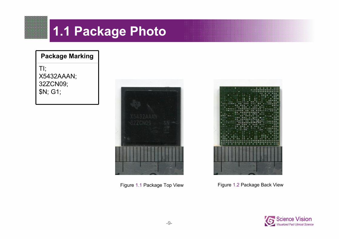
1.1 Package Photo
Package Marking
TI; X5432AAAN;32ZCN09; $N; G1;
Figure 1.1 Package Top View
-9-
Figure 1.2 Package Back View
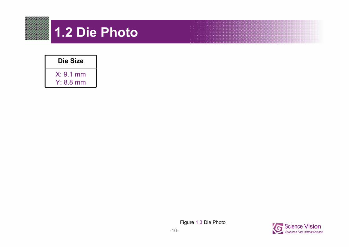
1.2 Die Photo
Die Size
X: 9.1 mmY: 8.8 mm
Figure 1.3 Die Photo-10-

2.0 General Structure Analysis
Description
2.1 Metal Layers Measurement Table2.2 Via Measurement Table2.3 Structure Analysis of Metal Layers2.4 Thickness of Metal8-9 Layers2.5 Thickness of Metal1-7 Layers
-11-

Description
ImagingAn optical microscope is used to image overview of the device. A Scanning Electron Microscope (SEM) is used to image cross section of the device. An Energy Dispersive X-Ray Spectroscopy (EDX) is used to measure the elements contained.
Sample PreparationHigh precision cross-section technique is used in this part. Prior to SEM analysis, the sample is chemically treated to either delineate different dielectric layers or to delineate P-type and N-type regions within the silicon substrate. After a specimen is delayered to the desired layer, a thin layer of Pt is sputter coated on the surface to be imaged in order to minimize sample charging. The results of this analysis are presented in this section.
Results of AnalysisGeneral Structure Analysis: The related information is shown through Figure 2.1 to Figure 2.3.
-12-

2.1 Metal Layers Measurement Table
Items Thickness MaterialMetal 9
Metal 8
Metal 7
Metal 6
Metal 5
Metal 4
Metal 3
Metal 2
Metal 1
-13-

2.2 Via Measurement Table
Items Thickness MaterialVia 8
Via 7
Via 6
Via 5
Via 4
Via 3
Via 2
Via 1
Contact
-14-

2.3 Structure Analysis of Metal Layers
Figure 2.1 Structure of Metal Layers SEM 5,000X-15-

2.4 Thickness of Metal 8-9 Layers
Thickness
Metal 9
Metal 8
Via 8
Via 7
Figure 2.2 Thickness of Metal8-9 Layers_SEM 5,000X
-16-

2.5 Thickness of Metal1-7 Layers
Thickness
Metal 7
Metal 6
Metal 5
Metal 4
Metal 3
Metal 2
Metal 1
Via 6
Via 5
Via 4
Via 3
Via 2
Via 1
Contact
Figure 2.3 Thickness of Metal1-7 Layers_SEM 18.28KX
-17-

3.0 SRAM Cell Structure Analysis
Description
3.1 Structure Analysis of 6T SRAM Cell 3.2 Structure Analysis of 8T SRAM Cell
-18-

Description
ImagingAn optical microscope is used to image overview of the device. And a Scanning Electron Microscope (SEM) is used to image cross section of the device.
Sample PreparationHigh precision cross-section technique is used in this part. Prior to SEM analysis, the sample is chemically treated to either delineate different dielectric layers or to delineate P-type and N-type regions within the silicon substrate. After a specimen is delayered to the desired layer, a thin layer of Pt is sputter coated on the surface to be imaged in order to minimize sample charging. The results of this analysis are presented in this section.
Results of AnalysisCross Section of 6T SRAM Cell : The related information is shown in Figure 3.1.1 to Figure 3.1.4.Cross Section of 8T SRAM Cell : The related information is shown in Figure 3.2.1 to Figure 3.2.2.
-19-

3.1 Structure Analysis of 6T SRAM Cell
Figure 3.1 Position of 6T SRAM Cell Cross Section Analysis
-20-
X1 X2

3.1.1 Vertical Structure of X1
Figure 3.1.1 Vertical Structure of X1_SEM 45.0KX
-21-

3.1.2 Size of X1 Position
Figure 3.1.2 Size of X1 Position_SEM 45.0KX
-22-
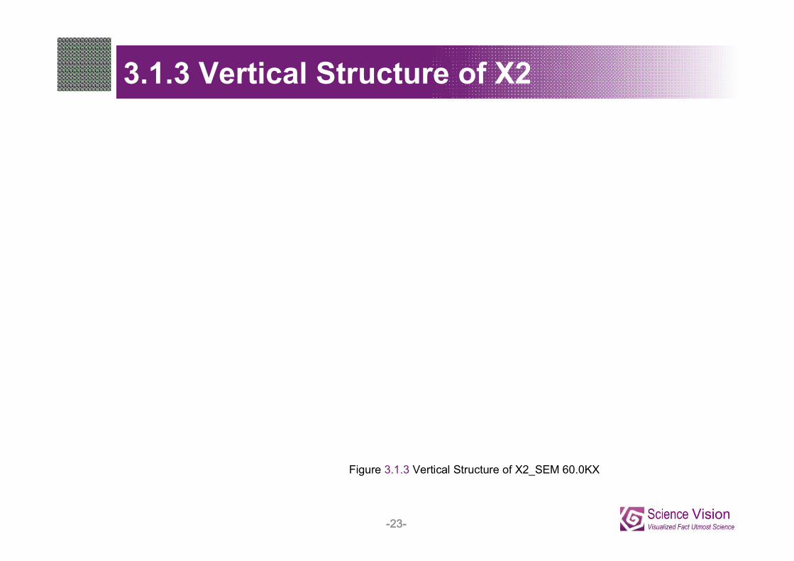
3.1.3 Vertical Structure of X2
Figure 3.1.3 Vertical Structure of X2_SEM 60.0KX
-23-
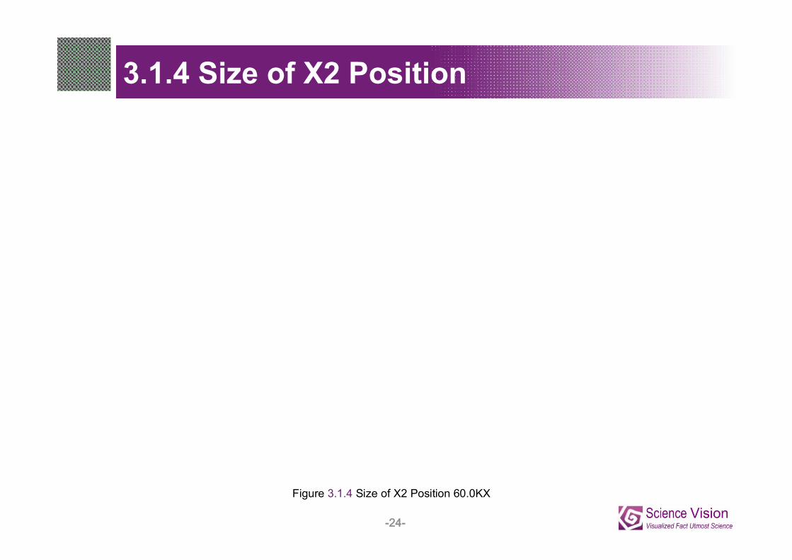
3.1.4 Size of X2 Position
Figure 3.1.4 Size of X2 Position 60.0KX
-24-

3.2 Structure Analysis of 8T SRAM Cell
Figure 3.2 Position of 8T SRAM Cell Cross Section Analysis
-25-
T1 T2
T3T4
T6 T7
T5 T8
X3

3.2.1 Vertical Structure of X3
Figure 3.2.1 Vertical Structure of X3_SEM 32.0KX
-26-

3.2.2 Size of X3 Position
Figure 3.2.2 Size of X3 Position_SEM 32.0KX
-27-