st16c554/554d - exar which allows easy integration with motorola processors. the ... cdb# rib# rxb...
TRANSCRIPT

ST16C554/554D2.97V TO 5.5V QUAD UART WITH 16-BYTE FIFO
JUNE 2006 REV. 4.0.1
GENERAL DESCRIPTION The ST16C554/554D (554) is a quad Universal Asynchronous Receiver and Transmitter (UART) with 16 bytes of transmit and receive FIFOs, selectable receive FIFO trigger levels and data rates of up to 1.5 Mbps. Each UART has a set of registers that provide the user with operating status and control, receiver error indications, and modem serial interface controls. An internal loopback capability allows onboard diagnostics. The 554 is available in a 64-pin LQFP and a 68-pin PLCC package. The 64-pin package only offers the 16 mode interface, but the 68-pin package offers an additional 68 mode interface which allows easy integration with Motorola processors. The ST16C554CQ64 (64-pin) offers three state interrupt output while the ST16C554DCQ64 provides continuous interrupt output. The 554 combines the package interface modes of the 16C554 and 68C554 on a single integrated chip.
FEATURES
• Pin-to-pin compatible with the industry standard ST16C454, ST68C454, ST68C554, TI’s TL16C554A and Philips’ SC16C554B
• Intel or Motorola Data Bus Interface select
• Four independent UART channels
■ Register Set Compatible to 16C550■ Data rates of up to 1.5 Mbps at 5 V ■ Data rates of up to 500 Kbps at 3.3V■ 16 byte Transmit FIFO■ 16 byte Receive FIFO with error tags■ 4 Selectable RX FIFO Trigger Levels■ Full modem interface
• 2.97V to 5.5V supply operation
• Crystal oscillator or external clock input
APPLICATIONS
• Portable Appliances
• Telecommunication Network Routers
• Ethernet Network Routers
• Cellular Data Devices
• Factory Automation and Process Controls
Exar Corporation 48720 Kato Road, Fremont CA, 94538 • (510) 668-7000 • FAX (510) 668-7017 • www.exar.com
FIGURE 1. ST16C554 BLOCK DIAGRAM
XTAL1XTAL2
Crystal Osc / Buffer
Data BusInterface
UART Channel A16 Byte TX FIFO
16 Byte RX FIFOBRG
IRENDECTX & RX
UARTRegs
2.97 V to 5.5V VCCGND
TXB, RXB, IRTXB, DTRB#,DSRB#, RTSB#, CTSB#,CDB#, RIB#
UART Channel B(same as Channel A)
A2:A0D7:D0
CSA#
16/68#
CSB#
INTAINTB
IOW#IOR#
Reset
INTSEL
TXRDY# A-DRXRDY# A-D
UART Channel C(same as Channel A)
TXA, RXA, IRTXA, DTRA#,DSRA#, RTSA#, CTSA#,CDA#, RIA#
TXC, RXC, IRTXC, DTRC#,DSRC#, RTSC#, CTSC#,CDC#, RIC#
UART Channel D(same as Channel A)
TXD, RXD, IRTXD, DTRD#,DSRD#, RTSD#, CTSD#,CDD#, RID#
CSC#CSD#
INTCINTD

ST16C554/554D 2.97V TO 5.5V QUAD UART WITH 16-BYTE FIFO REV. 4.0.1
FIGURE 2. PIN OUT ASSIGNMENT
ORDERING INFORMATION
PART NUMBER PACKAGEOPERATING TEMPERATURE
RANGEDEVICE STATUS
ST16C554CQ64 64-Lead LQFP 0°C to +70°C Active
ST16C554DCQ64 64-Lead LQFP 0°C to +70°C Active
ST16C554DIQ64 64-Lead LQFP -40°C to +85°C Active
ST16C554DCJ68 68-Lead PLCC 0°C to +70°C Active
ST16C554DIJ68 68-Lead PLCC -40°C to +85°C Active
ST68C554CJ68 68-Lead PLCC 0°C to +70°C Active
ST68C554IJ68 68-Lead PLCC -40°C to +85°C Active
9 8 7 6 5 4 3 2 1 68 67 66 65 64 63 62 63
10
11
12
13
14
15
16
17
18
19
20
21
22
23
24
25
26
60
59
58
57
56
55
54
53
52
51
50
49
48
47
46
45
44
27 28 29 30 31 32 33 34 35 36 37 38 39 40 41 42 43
DSRA#
CTSA#
DTRA#
VCC
RTSA#
INTA
CSA#
TXA
IOW#
TXB
CSB#
INTB
RTSB#
GND
DTRB#
CTSB#
DSRB#
CD
B#
RIB
#
RXB
VC
C
16/6
8# A2
A1
A0
XTA
L1
XTA
L2
RES
ET
RXR
DY
#
TXR
DY
#
GN
D
RXC
RIC
#
CD
C#
DSRD#
CTSD#
DTRD#
GND
RTSD#
INTD
CSD#
TXD
IOR#
TXC
CSC#
INTC
RTSC#
VCC
DTRC#
CTSC#
DSRC#
CD
A#
RIA
#
RXA
GN
D
D7
D6
D5
D4
D3
D2
D1
D0
INTS
EL
VC
C
RX
D
RID
#
CD
D#
ST16C55468-pin PLCCIntel Mode
(16/68# pin connected to VCC)
9 8 7 6 5 4 3 2 1 68 67 66 65 64 63 62 63
10
11
12
13
14
15
16
17
18
19
20
21
22
23
24
25
26
60
59
58
57
56
55
54
53
52
51
50
49
48
47
46
45
44
27 28 29 30 31 32 33 34 35 36 37 38 39 40 41 42 43
DSRA#
CTSA#
DTRA#
VCC
RTSA#
IRQ#
CS#
TXA
R/W#
TXB
A3
N.C.
RTSB#
GND
DTRB#
CTSB#
DSRB#
CD
B#
RIB
#
RXB
VCC
16/6
8# A2 A1 A0
XTAL
1
XTAL
2
RES
ET
RXR
DY#
TXR
DY#
GN
D
RXC
RIC
#
CD
C#
DSRD#
CTSD#
DTRD#
GND
RTSD#
N.C.
N.C.
TXD
N.C.
TXC
A4
N.C.
RTSC#
VCC
DTRC#
CTSC#
DSRC#
CD
A#
RIA
#
RXA
GN
D
D7
D6
D5
D4
D3
D2
D1
D0
GN
D
VC
C
RXD
RID
#
CD
D#
ST16C55468-pin PLCC
Motorola Mode(16/68# pin connected to GND)
1
2
3
4
5
6
7
8
9
10
11
12
13
14
15
16
17 18 19 20 21 22 23 24 25 26 27 28 29 30 31 32
48
47
46
45
44
43
42
41
40
39
38
37
36
35
34
33
64 63 62 61 60 59 58 57 56 55 54 53 52 51 50 49
DSRA#
CTSA#
DTRA#
VCC
RTSA#
INTA
CSA#
TXA
IOW#
TXB
CSB#
INTB
RTSB#
GND
DTRB#
CTSB#
DS
RB
#
CD
B#
RIB
#
RX
B
VC
C A2 A1 A0
XTAL
1
XTA
L2
RE
SE
T
GN
D
RXC
RIC
#
CD
C#
DS
RC
#
DSRD#
CTSD#
DTRD#
GND
RTSD#
INTD
CSD#
TXD
IOR#
TXC
CSC#
INTC
RTSC#
VCC
DTRC#
CTSC#
CD
A#
RIA
#
RX
A
GN
D
D7
D6
D5
D4
D3
D2
D1
D0
VCC
RX
D
RID
#
CD
D#
ST16C554/554D64-pin TQFP
Intel Mode Only
9 8 7 6 5 4 3 2 1 68 67 66 65 64 63 62 63
10
11
12
13
14
15
16
17
18
19
20
21
22
23
24
25
26
60
59
58
57
56
55
54
53
52
51
50
49
48
47
46
45
44
27 28 29 30 31 32 33 34 35 36 37 38 39 40 41 42 43
DSRA#
CTSA#
DTRA#
VCC
RTSA#
IRQ#
CS#
TXA
R/W#
TXB
A3
N.C.
RTSB#
GND
DTRB#
CTSB#
DSRB#
CD
B#
RIB
#
RXB
VCC
GN
D A2 A1 A0
XTAL
1
XTAL
2
RES
ET
RXR
DY#
TXR
DY#
GN
D
RXC
RIC
#
CD
C#
DSRD#
CTSD#
DTRD#
GND
RTSD#
N.C.
N.C.
TXD
N.C.
TXC
A4
N.C.
RTSC#
VCC
DTRC#
CTSC#
DSRC#
CD
A#
RIA
#
RXA
GN
D
D7
D6
D5
D4
D3
D2
D1
D0
GN
D
VC
C
RXD
RID
#
CD
D#
ST68C55468-pin PLCC
Motorola Mode Only
2

ST16C554/554DREV. 4.0.1 2.97V TO 5.5V QUAD UART WITH 16-BYTE FIFO
3
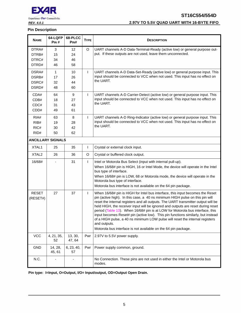
PIN DESCRIPTIONS Pin Description
NAME64-LQFP
PIN #68-PLCC
PIN# TYPE DESCRIPTION
DATA BUS INTERFACE
A2A1A0
222324
323334
I Address data lines [2:0]. These 3 address lines select one of the internal regis-ters in UART channel A-D during a data bus transaction.
D7D6D5D4D3D2D1D0
6059585756555453
54321
686766
I/O Data bus lines [7:0] (bidirectional).
IOR#(VCC)
40 52 I When 16/68# pin is HIGH, the Intel bus interface is selected and this input becomes read strobe (active low). The falling edge instigates an internal read cycle and retrieves the data byte from an internal register pointed by the address lines [A2:A0], puts the data byte on the data bus to allow the host processor to read it on the rising edge.When 16/68# pin is LOW, the Motorola bus interface is selected and this input is not used and should be connected to VCC.
IOW#(R/W#)
9 18 I When 16/68# pin is HIGH, it selects Intel bus interface and this input becomes write strobe (active low). The falling edge instigates the internal write cycle and the rising edge transfers the data byte on the data bus to an internal register pointed by the address lines.When 16/68# pin is LOW, the Motorola bus interface is selected and this input becomes read (HIGH) and write (LOW) signal.
CSA#(CS#)
7 16 I When 16/68# pin is HIGH, this input is chip select A (active low) to enable chan-nel A in the device.When 16/68# pin is LOW, this input becomes the chip select (active low) for the Motorola bus interface.
CSB#(A3)
11 20 I When 16/68# pin is HIGH, this input is chip select B (active low) to enable chan-nel B in the device.When 16/68# pin is LOW, this input becomes address line A3 which is used for channel selection in the Motorola bus interface.
CSC#(A4)
38 50 I When 16/68# pin is HIGH, this input is chip select C (active low) to enable chan-nel C in the device.When 16/68# pin is LOW, this input becomes address line A4 which is used for channel selection in the Motorola bus interface.
CSD#(VCC)
42 54 I When 16/68# pin is HIGH, this input is chip select D (active low) to enable chan-nel D in the device. When 16/68# pin is LOW, this input is not used and should be connected VCC.

ST16C554/554D 2.97V TO 5.5V QUAD UART WITH 16-BYTE FIFO REV. 4.0.1
4
INTA(IRQ#)
6 15 O(OD)
When 16/68# pin is HIGH for Intel bus interface, this ouput becomes channel A interrupt output. The output state is defined by the user and through the soft-ware setting of MCR[3]. INTA is set to the active mode when MCR[3] is set to a logic 1. INTA is set to the three state mode when MCR[3] is set to a logic 0 (default). See MCR[3]. When 16/68# pin is LOW for Motorola bus interface, this output becomes device interrupt output (active low, open drain). An external pull-up resistor is required for proper operation.
INTBINTCINTD(N.C.)
123743
214955
O When 16/68# pin is HIGH for Intel bus interface, these ouputs become the inter-rupt outputs for channels B, C, and D. The output state is defined by the user through the software setting of MCR[3]. The interrupt outputs are set to the active mode when MCR[3] is set to a logic 1 and are set to the three state mode when MCR[3] is set to a logic 0 (default). See MCR[3].When 16/68# pin is LOW for Motorola bus interface, these outputs are unused and will stay at logic zero level. Leave these outputs unconnected.
INTSEL - 65 I Interrupt Select (active high, input with internal pull-down). When 16/68# pin is HIGH for Intel bus interface, this pin can be used in conjunc-tion with MCR bit-3 to enable or disable the INT A-D pins or override MCR bit-3 and enable the interrupt outputs. Interrupt outputs are enabled continuously when this pin is HIGH. MCR bit-3 enables and disables the interrupt output pins. In this mode, MCR bit-3 is set to a logic 1 to enable the continuous output. See MCR bit-3 description for full detail. This pin must be LOW in the Motorola bus interface mode. For the 64 pin packages, this pin is bonded to VCC inter-nally in the ST16C554DCQ64 so the INT outputs operate in the continuous interrupt mode. This pin is bonded to GND internally in the ST16C554CQ64 and therefore requires setting MCR bit-3 for enabling the interrupt output pins.
TXRDY# - 39 O Transmitter Ready (active low). This output is a logically ANDed status of TXRDY# A-D. See Table 5. If this output is unused, leave it unconnected.
RXRDY# - 38 O Receiver Ready (active low). This output is a logically ANDed status of RXRDY# A-D. See Table 5. If this output is unused, leave it unconnected.
MODEM OR SERIAL I/O INTERFACE
TXATXBTXCTXD
8103941
17195153
O UART channels A-D Transmit Data and infrared transmit data. In this mode, the TX signal will be HIGH during reset, or idle (no data).
RXARXBRXCRXD
62202951
7294163
I UART channel A-D Receive Data. Normal receive data input must idle HIGH.
RTSA#RTSB#RTSC#RTSD#
5133644
14224856
O UART channels A-D Request-to-Send (active low) or general purpose output. If these outputs are not used, leave them unconnected.
CTSA#CTSB#CTSC#CTSD#
2163347
11254559
I UART channels A-D Clear-to-Send (active low) or general purpose input. These inputs should be connected to VCC when not used.
Pin Description
NAME64-LQFP
PIN #68-PLCC
PIN# TYPE DESCRIPTION
ST16C554/554DREV. 4.0.1 2.97V TO 5.5V QUAD UART WITH 16-BYTE FIFO
Pin type: I=Input, O=Output, I/O= Input/output, OD=Output Open Drain.
DTRA#DTRB#DTRC#DTRD#
3153446
12244658
O UART channels A-D Data-Terminal-Ready (active low) or general purpose out-put. If these outputs are not used, leave them unconnected.
DSRA#DSRB#DSRC#DSRD#
1173248
10264460
I UART channels A-D Data-Set-Ready (active low) or general purpose input. This input should be connected to VCC when not used. This input has no effect on the UART.
CDA#CDB#CDC#CDD#
64183149
9274361
I UART channels A-D Carrier-Detect (active low) or general purpose input. This input should be connected to VCC when not used. This input has no effect on the UART.
RIA#RIB#RIC#RID#
63193050
8284262
I UART channels A-D Ring-Indicator (active low) or general purpose input. This input should be connected to VCC when not used. This input has no effect on the UART.
ANCILLARY SIGNALS
XTAL1 25 35 I Crystal or external clock input.
XTAL2 26 36 O Crystal or buffered clock output.
16/68# - 31 I Intel or Motorola Bus Select (input with internal pull-up). When 16/68# pin is HIGH, 16 or Intel Mode, the device will operate in the Intel bus type of interface. When 16/68# pin is LOW, 68 or Motorola mode, the device will operate in the Motorola bus type of interface. Motorola bus interface is not available on the 64 pin package.
RESET(RESET#)
27 37 I When 16/68# pin is HIGH for Intel bus interface, this input becomes the Reset pin (active high). In this case, a 40 ns minimum HIGH pulse on this pin will reset the internal registers and all outputs. The UART transmitter output will be held HIGH, the receiver input will be ignored and outputs are reset during reset period (Table 13). When 16/68# pin is at LOW for Motorola bus interface, this input becomes Reset# pin (active low). This pin functions similarly, but instead of a HIGH pulse, a 40 ns minimum LOW pulse will reset the internal registers and outputs.Motorola bus interface is not available on the 64 pin package.
VCC 4, 21, 35, 52
13, 30, 47, 64
Pwr 2.97V to 5.5V power supply.
GND 14, 28, 45, 61
6, 23, 40, 57
Pwr Power supply common, ground.
N.C. - - No Connection. These pins are not used in either the Intel or Motorola bus modes.
Pin Description
NAME64-LQFP
PIN #68-PLCC
PIN# TYPE DESCRIPTION
5

ST16C554/554D 2.97V TO 5.5V QUAD UART WITH 16-BYTE FIFO REV. 4.0.1
1.0 PRODUCT DESCRIPTION
The ST16C554 (554) integrates the functions of 4 enhanced 16C550 Universal Asynchrounous Receiver and Transmitter (UART). Each UART is independently controlled and has its own set of device configuration registers. The configuration registers set is 16550 UART compatible for control, status and data transfer. Additionally, each UART channel has 16 bytes of transmit and receive FIFOs, programmable baud rate generator and data rate up to 1.5 Mbps at 5V. The ST16C554 can operate from 2.97 to 5.5 volts. The 554 is fabricated with an advanced CMOS process.
Enhanced FIFO
The 554 QUART provides a solution that supports 16 bytes of transmit and receive FIFO memory, instead of one byte in the ST16C454. The 554 is designed to work with high performance data communication systems, that require fast data processing time. Increased performance is realized in the 554 by the larger transmit and receive FIFOs and Receiver FIFO trigger level control. This allows the external processor to handle more networking tasks within a given time. This increases the service interval giving the external CPU additional time for other applications and reducing the overall UART interrupt servicing time.
Data Bus Interface, Intel or Motorola Type
The 554 provides a single host interface for all 4 UARTs and supports Intel or Motorola microprocessor (CPU) data bus interface. The Intel bus compatible interface allows direct interconnect to Intel compatible type of CPUs using IOR#, IOW# and CSA#, CSB#, CSC# and CSD# inputs for data bus operation. The Motorola bus compatible interface instead uses the R/W#, CS#, A3 and A4 signals for data bus transactions. Few data bus interface signals change their functions depending on user’s selection, see pin description for details. The Intel and Motorola bus interface selection is made through the 16/68# (pin 31 of the PLCC package).
Data Rate
The 554 is capable of operation up to 1.5 Mbps at 5V. The device can operate at 5V with a crystal or external clock of up to 24 MHz. With a typical crystal of 14.7456 MHz and through a software option, the user can set the sampling rate for data rates of up to 921.6 Kbps.
Enhanced Features
The rich feature set of the 554 is available through the internal registers. Selectable receive FIFO trigger levels, programmable baud rates, infrared encoder/decoder interface and modem interface controls are all standard features. In the 16 mode INTSEL and MCR bit-3 can be configured to provide a software controlled or continuous interrupt capability. For backward compatibility to the ST16C554, the 64-pin LQFP does not have the INTSEL pin. Instead, two different LQFP packages are offered. The ST16C554DIV operates in the continuous interrupt enable mode by internally bonding INTSEL to VCC. The ST16C554IV operates in conjunction with MCR bit-3 by internally bonding INTSEL to GND.
6

ST16C554/554DREV. 4.0.1 2.97V TO 5.5V QUAD UART WITH 16-BYTE FIFO
2.0 FUNCTIONAL DESCRIPTIONS
2.1 CPU Interface
The CPU interface is 8 data bits wide with 3 address lines and control signals to execute data bus read and write transactions. The 554 data interface supports the Intel compatible types of CPUs and it is compatible to the industry standard 16C550 UART. No clock (oscillator nor external clock) is required for a data bus transaction. Each bus cycle is asynchronous using CS# A-D, IOR# and IOW# or CS#, R/W#, A4 and A3 inputs. All four UART channels share the same data bus for host operations. A typical data bus interconnection for Intel and Motorola mode is shown in Figure 3.
FIGURE 3. ST16C554 TYPICAL INTEL/MOTOROLA DATA BUS INTERCONNECTIONS
VCCVCC
DSRA#CTSA#RTSA#DTRA#
RXATXA
RIA#CDA#
GND
A0A1A2
UART_CSA#UART_CSB#
IOR#IOW#
D0D1D2D3D4D5D6D7
A0A1A2
CSA#CSB#
D0D1D2D3D4D5D6D7
IOR#IOW#
UARTChannel A
UARTChannel B
UART_INTBUART_INTA
INTBINTA
UART_RESET RESET
Serial Interface ofRS-232
Serial Interface ofRS-232
Intel Data Bus (16 Mode) Interconnections
UARTChannel C
UARTChannel D
Similarto Ch A
Similarto Ch A
Similarto Ch A
UART_INTDUART_INTC
INTDINTC
UART_CSC#UART_CSD#
CSC#CSD#
VCC 16/68#
VCCVCC
GND
A0A1A2
UART_CS#
A3
R/W#
D0D1D2D3D4D5D6D7
A0A1A2
CSA#
CSB#
D0D1D2D3D4D5D6D7
IOR#IOW#
UART_IRQ#INTBINTA
RESET#
Serial Interface ofRS-232
Serial Interface ofRS-232
Motorola Data Bus (68 Mode) Interconnections
VCC
UART_RESET#
(no connect)
DSRA#CTSA#RTSA#DTRA#
RXATXA
RIA#CDA#
UARTChannel A
UARTChannel B
UARTChannel C
Similarto Ch A
Similarto Ch A
Similarto Ch AINTC(no connect)
INTD(no connect)
A4 CSC#CSD#VCC
16/68#
UARTChannel D
VCC
7
ST16C554/554D 2.97V TO 5.5V QUAD UART WITH 16-BYTE FIFO REV. 4.0.1
2.2 Device Reset
The RESET input resets the internal registers and the serial interface outputs in all channels to their default state (see Table 13). An active high pulse of longer than 40 ns duration will be required to activate the reset function in the device. Following a power-on reset or an external reset, the 554 is software compatible with previous generation of UARTs, 16C454 and 16C554.
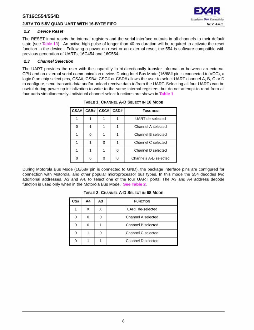
2.3 Channel Selection
The UART provides the user with the capability to bi-directionally transfer information between an external CPU and an external serial communication device. During Intel Bus Mode (16/68# pin is connected to VCC), a logic 0 on chip select pins, CSA#, CSB#, CSC# or CSD# allows the user to select UART channel A, B, C or D to configure, send transmit data and/or unload receive data to/from the UART. Selecting all four UARTs can be useful during power up initialization to write to the same internal registers, but do not attempt to read from all four uarts simultaneously. Individual channel select functions are shown in Table 1.
During Motorola Bus Mode (16/68# pin is connected to GND), the package interface pins are configured for connection with Motorola, and other popular microprocessor bus types. In this mode the 554 decodes two additional addresses, A3 and A4, to select one of the four UART ports. The A3 and A4 address decode function is used only when in the Motorola Bus Mode. See Table 2.
TABLE 1: CHANNEL A-D SELECT IN 16 MODE
CSA# CSB# CSC# CSD# FUNCTION
1 1 1 1 UART de-selected
0 1 1 1 Channel A selected
1 0 1 1 Channel B selected
1 1 0 1 Channel C selected
1 1 1 0 Channel D selected
0 0 0 0 Channels A-D selected
TABLE 2: CHANNEL A-D SELECT IN 68 MODE
CS# A4 A3 FUNCTION
1 X X UART de-selected
0 0 0 Channel A selected
0 0 1 Channel B selected
0 1 0 Channel C selected
0 1 1 Channel D selected
8

ST16C554/554DREV. 4.0.1 2.97V TO 5.5V QUAD UART WITH 16-BYTE FIFO
2.4 Channels A-D Internal Registers
Each UART channel in the 554 has a set of enhanced registers for controlling, monitoring and data loading and unloading. The configuration register set is compatible to those already available in the standard single 16C550. These registers function as data holding registers (THR/RHR), interrupt status and control registers (ISR/IER), a FIFO control register (FCR), receive line status and control registers (LSR/LCR), modem status and control registers (MSR/MCR), programmable data rate (clock) divisor registers (DLL/DLM), and a user accessible scratchpad register (SPR). All the register functions are discussed in full detail later in “Section 3.0, UART INTERNAL REGISTERS” on page 15.
2.5 INT Ouputs for Channels A-D
The interrupt outputs change according to the operating mode and enhanced features setup. Table 3 and 4summarize the operating behavior for the transmitter and receiver. Also see Figure 17 through 22.
2.6 DMA Mode
The device does not support direct memory access. The DMA Mode (a legacy term) in this document does not mean “direct memory access” but refers to data block transfer operation. The DMA mode affects the state of the RXRDY# A-D and TXRDY# A-D output pins. The transmit and receive FIFO trigger levels provide additional flexibility to the user for block mode operation. The LSR bits 5-6 provide an indication when the transmitter is empty or has an empty location(s) for more data. The user can optionally operate the transmit and receive FIFO in the DMA mode (FCR bit-3 = 1). When the transmit and receive FIFOs are enabled and the DMA mode is disabled (FCR bit-3 = 0), the 554 is placed in single-character mode for data transmit or receive operation. When DMA mode is enabled (FCR bit-3 = 1), the user takes advantage of block mode operation by
TABLE 3: INT PIN OPERATION FOR TRANSMITTER FOR CHANNELS A-D
FCR BIT-0 = 0 (FIFO DISABLED)
FCR BIT-0 = 1 (FIFO ENABLED)
FCR Bit-3 = 0 (DMA Mode Disabled)
FCR Bit-3 = 1(DMA Mode Enabled)
INT Pin LOW = a byte in THRHIGH = THR empty
LOW = FIFO above trigger levelHIGH = FIFO below trigger level or FIFO empty
LOW = FIFO above trigger levelHIGH = FIFO below trigger level or FIFO empty
TABLE 4: INT PIN OPERATION FOR RECEIVER FOR CHANNELS A-D
FCR BIT-0 = 0 (FIFO DISABLED)
FCR BIT-0 = 1 (FIFO ENABLED)
FCR Bit-3 = 0 (DMA Mode Disabled)
FCR Bit-3 = 1(DMA Mode Enabled)
INT Pin LOW = no dataHIGH = 1 byte
LOW = FIFO below trigger levelHIGH = FIFO above trigger level
LOW = FIFO below trigger levelHIGH = FIFO above trigger level
9
ST16C554/554D 2.97V TO 5.5V QUAD UART WITH 16-BYTE FIFO REV. 4.0.1
loading or unloading the FIFO in a block sequence determined by the programmed trigger level. The following table show their behavior. Also see Figure 17 through 22.
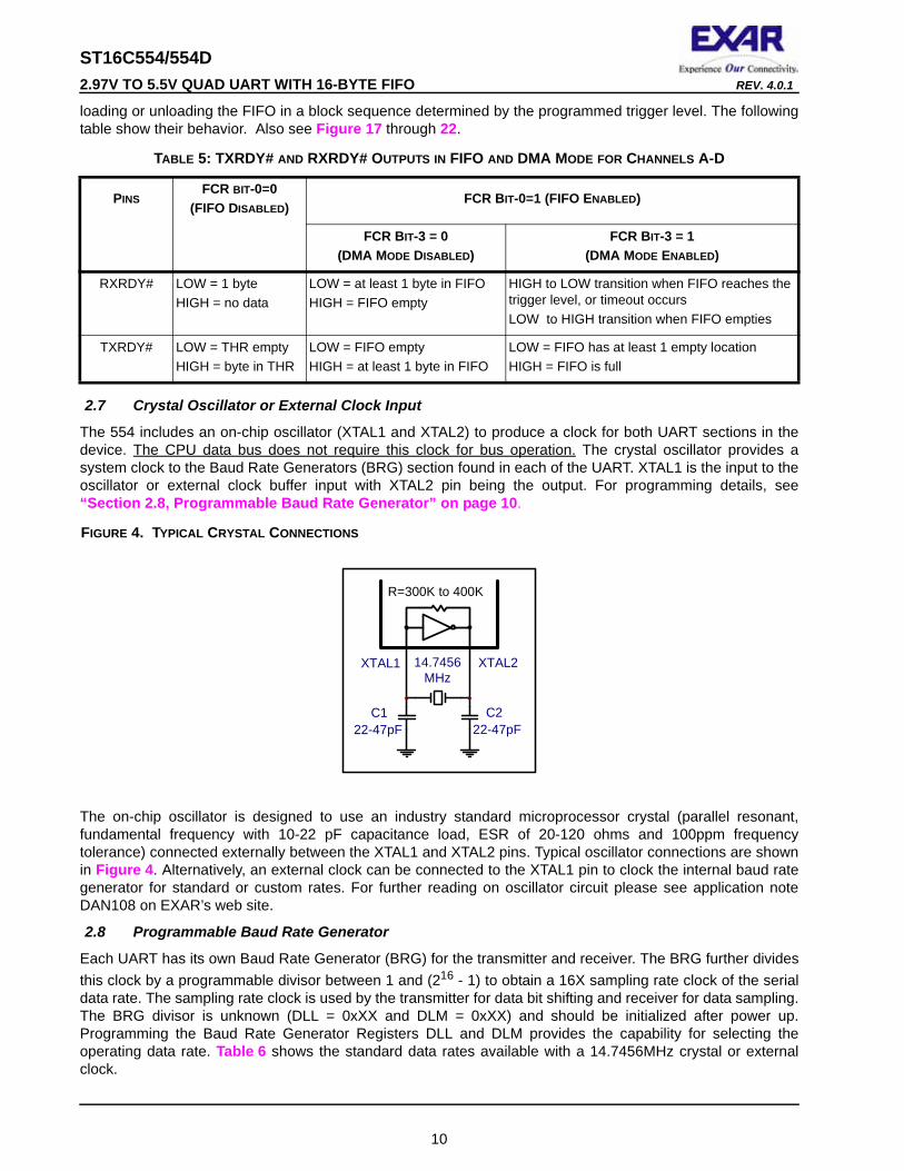
2.7 Crystal Oscillator or External Clock Input
The 554 includes an on-chip oscillator (XTAL1 and XTAL2) to produce a clock for both UART sections in the device. The CPU data bus does not require this clock for bus operation. The crystal oscillator provides a system clock to the Baud Rate Generators (BRG) section found in each of the UART. XTAL1 is the input to the oscillator or external clock buffer input with XTAL2 pin being the output. For programming details, see “Section 2.8, Programmable Baud Rate Generator” on page 10.
The on-chip oscillator is designed to use an industry standard microprocessor crystal (parallel resonant, fundamental frequency with 10-22 pF capacitance load, ESR of 20-120 ohms and 100ppm frequency tolerance) connected externally between the XTAL1 and XTAL2 pins. Typical oscillator connections are shown in Figure 4. Alternatively, an external clock can be connected to the XTAL1 pin to clock the internal baud rate generator for standard or custom rates. For further reading on oscillator circuit please see application note DAN108 on EXAR’s web site.
2.8 Programmable Baud Rate Generator
Each UART has its own Baud Rate Generator (BRG) for the transmitter and receiver. The BRG further divides this clock by a programmable divisor between 1 and (216 - 1) to obtain a 16X sampling rate clock of the serial data rate. The sampling rate clock is used by the transmitter for data bit shifting and receiver for data sampling. The BRG divisor is unknown (DLL = 0xXX and DLM = 0xXX) and should be initialized after power up. Programming the Baud Rate Generator Registers DLL and DLM provides the capability for selecting the operating data rate. Table 6 shows the standard data rates available with a 14.7456MHz crystal or external clock.
TABLE 5: TXRDY# AND RXRDY# OUTPUTS IN FIFO AND DMA MODE FOR CHANNELS A-D
PINSFCR BIT-0=0
(FIFO DISABLED)FCR BIT-0=1 (FIFO ENABLED)
FCR BIT-3 = 0(DMA MODE DISABLED)
FCR BIT-3 = 1(DMA MODE ENABLED)
RXRDY# LOW = 1 byteHIGH = no data
LOW = at least 1 byte in FIFO HIGH = FIFO empty
HIGH to LOW transition when FIFO reaches the trigger level, or timeout occurs LOW to HIGH transition when FIFO empties
TXRDY# LOW = THR emptyHIGH = byte in THR
LOW = FIFO emptyHIGH = at least 1 byte in FIFO
LOW = FIFO has at least 1 empty locationHIGH = FIFO is full
FIGURE 4. TYPICAL CRYSTAL CONNECTIONS
C122-47pF
C222-47pF
14.7456MHz
XTAL1 XTAL2
R=300K to 400K
10

ST16C554/554DREV. 4.0.1 2.97V TO 5.5V QUAD UART WITH 16-BYTE FIFO
2.9 Transmitter
The transmitter section comprises of an 8-bit Transmit Shift Register (TSR) and 16 bytes of FIFO which includes a byte-wide Transmit Holding Register (THR). TSR shifts out every data bit with the 16X internal sampling clock. A bit time is 16X clock periods. The transmitter sends the start-bit followed by the number of data bits, inserts the proper parity-bit if enabled, and adds the stop-bit(s). The status of the FIFO and TSR are reported in the Line Status Register (LSR bit-5 and bit-6).
2.9.1 Transmit Holding Register (THR) - Write Only
The transmit holding register is an 8-bit register providing a data interface to the host processor. The host writes transmit data byte to the THR to be converted into a serial data stream including start-bit, data bits, parity-bit and stop-bit(s). The least-significant-bit (Bit-0) becomes first data bit to go out. The THR is the input register to the transmit FIFO of 16 bytes when FIFO operation is enabled by FCR bit-0. Every time a write operation is made to the THR, the FIFO data pointer is automatically bumped to the next sequential data location.
FIGURE 5. BAUD RATE GENERATOR
TABLE 6: TYPICAL DATA RATES WITH A 14.7456 MHZ CRYSTAL OR EXTERNAL CLOCK
OUTPUT Data Rate MCR Bit-7=1
OUTPUT Data Rate MCR Bit-7=0
(DEFAULT)
DIVISOR FOR 16x Clock (Decimal)
DIVISOR FOR 16x Clock (HEX)
DLM PROGRAM
VALUE (HEX)
DLL PROGRAM
VALUE (HEX)
DATA RATE
ERROR (%)
100 400 2304 900 09 00 0
600 2400 384 180 01 80 0
1200 4800 192 C0 00 C0 0
2400 9600 96 60 00 60 0
4800 19.2k 48 30 00 30 0
9600 38.4k 24 18 00 18 0
19.2k 76.8k 12 0C 00 0C 0
38.4k 153.6k 6 06 00 06 0
57.6k 230.4k 4 04 00 04 0
115.2k 460.8k 2 02 00 02 0
230.4k 921.6k 1 01 00 01 0
XTAL1
XTAL2
CrystalOsc /Buffer
DLL and DLMRegisters
16 X SamplingRate Clock
to Transmitterand Receiver
To OtherChannels
Programmable BaudRate Generator Logic
11

ST16C554/554D 2.97V TO 5.5V QUAD UART WITH 16-BYTE FIFO REV. 4.0.1
2.9.2 Transmitter Operation in non-FIFO Mode
The host loads transmit data to THR one character at a time. The THR empty flag (LSR bit-5) is set when the data byte is transferred to TSR. THR flag can generate a transmit empty interrupt (ISR bit-1) when it is enabled by IER bit-1. The TSR flag (LSR bit-6) is set when TSR becomes completely empty.
2.9.3 Transmitter Operation in FIFO Mode
The host may fill the transmit FIFO with up to 16 bytes of transmit data. The THR empty flag (LSR bit-5) is set whenever the FIFO is empty. The THR empty flag can generate a transmit empty interrupt (ISR bit-1) when the FIFO becomes empty. The transmit empty interrupt is enabled by IER bit-1. The TSR flag (LSR bit-6) is set when TSR/FIFO becomes empty.
2.10 Receiver
The receiver section contains an 8-bit Receive Shift Register (RSR) and 16 bytes of FIFO which includes a byte-wide Receive Holding Register (RHR). The RSR uses the 16X clock for timing. It verifies and validates every bit on the incoming character in the middle of each data bit. On the falling edge of a start or false start bit, an internal receiver counter starts counting at the 16X clock rate. After 8 clocks the start bit period should be at the center of the start bit. At this time the start bit is sampled and if it is still LOW it is validated. Evaluating the start bit in this manner prevents the receiver from assembling a false character. The rest of the data bits and stop bits are sampled and validated in this same manner to prevent false framing. If there were any error(s), they are reported in the LSR register bits 2-4. Upon unloading the receive data byte from RHR, the receive FIFO pointer is bumped and the error tags are immediately updated to reflect the status of the data byte in RHR register. RHR can generate a receive data ready interrupt upon receiving a character or delay until it reaches the FIFO trigger level. Furthermore, data delivery to the host is guaranteed by a receive data ready time-out interrupt when data is not received for 4 word lengths as defined by LCR[1:0] plus 12 bits time. This is equivalent to 3.7-4.6 character times. The RHR interrupt is enabled by IER bit-0. See Figure 8 and Figure 9.
FIGURE 6. TRANSMITTER OPERATION IN NON-FIFO MODE
FIGURE 7. TRANSMITTER OPERATION IN FIFO MODE
TransmitHoldingRegister(THR)
Transmit Shift Register (TSR)
DataByte
LSB
MSB
THR Interrupt (ISR bit-1)Enabled by IER bit-1
TXNOFIFO1
16X Clock
Transmit Data Shift Register(TSR)
TransmitData Byte THR Interrupt (ISR bit-1)
when the TX FIFO becomes empty. FIFO is enabled by FCR bit-0 =1.
TransmitFIFO
16X Clock
TXFIFO1
12

ST16C554/554DREV. 4.0.1 2.97V TO 5.5V QUAD UART WITH 16-BYTE FIFO
2.10.1 Receive Holding Register (RHR) - Read-Only
The Receive Holding Register is an 8-bit register that holds a receive data byte from the Receive Shift Register. It provides the receive data interface to the host processor. The RHR register is part of the receive FIFO of 16 bytes by 11-bit wide, the 3 extra bits are for the 3 error tags to be reported in LSR register. When the FIFO is enabled by FCR bit-0, the RHR contains the first data character received by the FIFO. After the RHR is read, the next character byte is loaded into the RHR and the errors associated with the current data byte are immediately updated in the LSR bits 2-4.
FIGURE 8. RECEIVER OPERATION IN NON-FIFO MODE
FIGURE 9. RECEIVER OPERATION IN FIFO
Receive Data ShiftRegister (RSR)
ReceiveData Byteand Errors
RHR Interrupt (ISR bit-2)Receive Data
Holding Register(RHR)
RXFIFO1
16X Clock
Receive Data Characters
Data BitValidation
ErrorTags inLSR bits
4:2
Receive Data ShiftRegister (RSR)
RXFIFO 1
16X Clock
Err
or T
ags
(16-
sets
)Er
ror T
ags
inLS
R b
its 4
:2
Receive Data Characters
Data BitValidation
ReceiveData FIFO
ReceiveDataReceive Data
Byte and Errors
RHR Interrupt (ISR bit-2) programmed fordesired FIFO trigger level.FIFO is Enabled by FCR bit-0=1
Asking for stopping data when data fills above the flowcontrol trigger level to suspend remote transmitter.
Asking for sending data when data falls below the flowcontrol trigger level to restart remote transmitter.
16 bytes by 11-bit wideFIFO
FIFOTrigger=8
Data falls to4
Data fills to14
Example: - RX FIFO trigger level selected at 8 bytes
(See Note Below)
13

ST16C554/554D 2.97V TO 5.5V QUAD UART WITH 16-BYTE FIFO REV. 4.0.1
2.11 Internal Loopback
The 554 UART provides an internal loopback capability for system diagnostic purposes. The internal loopback mode is enabled by setting MCR register bit-4 to logic 1. All regular UART functions operate normally. Figure 10 shows how the modem port signals are re-configured. Transmit data from the transmit shift register output is internally routed to the receive shift register input allowing the system to receive the same data that it was sending. The TX pin is held HIGH or mark condition while RTS# and DTR# are de-asserted, and CTS#, DSR# CD# and RI# inputs are ignored. Caution: the RX input must be held HIGH during loopback test else upon exiting the loopback test the UART may detect and report a false “break” signal.
FIGURE 10. INTERNAL LOOP BACK IN CHANNEL A AND B
TX A-D
RX A-D
Mod
em /
Gen
eral
Pur
pose
Con
trol L
ogic
Inte
rnal
Dat
a B
us L
ines
and
Con
trol
Sig
nals
RTS# A-D
MCR bit-4=1
VCC
VCC
Transmit Shift Register(THR/FIFO)
Receive Shift Register(RHR/FIFO)
CTS# A-D
DTR# A-D
DSR# A-D
RI# A-D
CD# A-D
OP1#
OP2#
RTS#
CTS#
DTR#
DSR#
RI#
CD#
VCC
14
ST16C554/554DREV. 4.0.1 2.97V TO 5.5V QUAD UART WITH 16-BYTE FIFO
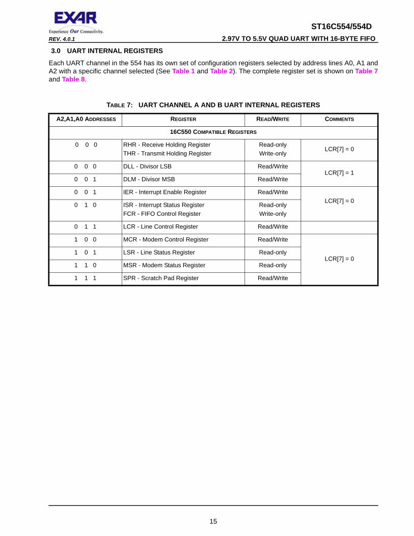
3.0 UART INTERNAL REGISTERS
Each UART channel in the 554 has its own set of configuration registers selected by address lines A0, A1 and A2 with a specific channel selected (See Table 1 and Table 2). The complete register set is shown on Table 7and Table 8.
TABLE 7: UART CHANNEL A AND B UART INTERNAL REGISTERS
A2,A1,A0 ADDRESSES REGISTER READ/WRITE COMMENTS
16C550 COMPATIBLE REGISTERS
0 0 0 RHR - Receive Holding Register THR - Transmit Holding Register
Read-onlyWrite-only
LCR[7] = 0
0 0 0 DLL - Divisor LSB Read/WriteLCR[7] = 1
0 0 1 DLM - Divisor MSB Read/Write
0 0 1 IER - Interrupt Enable Register Read/WriteLCR[7] = 0
0 1 0 ISR - Interrupt Status RegisterFCR - FIFO Control Register
Read-onlyWrite-only
0 1 1 LCR - Line Control Register Read/Write
1 0 0 MCR - Modem Control Register Read/Write
LCR[7] = 01 0 1 LSR - Line Status Register Read-only
1 1 0 MSR - Modem Status Register Read-only
1 1 1 SPR - Scratch Pad Register Read/Write
15

ST16C554/554D 2.97V TO 5.5V QUAD UART WITH 16-BYTE FIFO REV. 4.0.1
4.0 INTERNAL REGISTER DESCRIPTIONS
4.1 Receive Holding Register (RHR) - Read- Only
SEE”RECEIVER” ON PAGE 12.
4.2 Transmit Holding Register (THR) - Write-Only
SEE”TRANSMITTER” ON PAGE 11.
4.3 Interrupt Enable Register (IER) - Read/Write
The Interrupt Enable Register (IER) masks the interrupts from receive data ready, transmit empty, line status and modem status registers. These interrupts are reported in the Interrupt Status Register (ISR).
TABLE 8: INTERNAL REGISTERS DESCRIPTION.
ADDRESS
A2-A0REG
NAME
READ/WRITE
BIT-7 BIT-6 BIT-5 BIT-4 BIT-3 BIT-2 BIT-1 BIT-0 COMMENT
16C550 Compatible Registers
0 0 0 RHR RD Bit-7 Bit-6 Bit-5 Bit-4 Bit-3 Bit-2 Bit-1 Bit-0
LCR[7] = 0
0 0 0 THR WR Bit-7 Bit-6 Bit-5 Bit-4 Bit-3 Bit-2 Bit-1 Bit-0
0 0 1 IER RD/WR 0 0 0 0 Modem Stat. Int.
Enable
RX Line Stat. Int.
Enable
TX Empty
Int Enable
RX Data Int.
Enable
0 1 0 ISR RD FIFOs Enabled
FIFOs Enabled
0 0 INT Source Bit-3
INT Source
Bit-2
INT Source
Bit-1
INT Source
Bit-0
0 1 0 FCR WR RX FIFO Trigger
RX FIFO Trigger
0 0 DMA Mode
Enable
TX FIFO Reset
RX FIFO Reset
FIFOs Enable
0 1 1 LCR RD/WR Divisor Enable
Set TX Break
Set Parity
Even Parity
Parity Enable
Stop Bits
Word LengthBit-1
Word LengthBit-0
1 0 0 MCR RD/WR 0 0 0 Internal Lopback Enable
INT Output Enable(OP2#)
Rsvd(OP1#)
RTS# Output Control
DTR# Output Control
LCR[7] = 0 1 0 1 LSR RD/WR RX
FIFO Global Error
THR & TSR
Empty
THR Empty
RX Break RX Framing
Error
RX Parity Error
RX Over-run
Error
RX Data
Ready
1 1 0 MSR RD/WR CD# Input
RI# Input
DSR# Input
CTS# Input
Delta CD#
Delta RI#
Delta DSR#
Delta CTS#
1 1 1 SPR RD/WR Bit-7 Bit-6 Bit-5 Bit-4 Bit-3 Bit-2 Bit-1 Bit-0
Baud Rate Generator Divisor
0 0 0 DLL RD/WR Bit-7 Bit-6 Bit-5 Bit-4 Bit-3 Bit-2 Bit-1 Bit-0 LCR[7]=1LCR≠0xBF
0 0 1 DLM RD/WR Bit-7 Bit-6 Bit-5 Bit-4 Bit-3 Bit-2 Bit-1 Bit-0
16

ST16C554/554DREV. 4.0.1 2.97V TO 5.5V QUAD UART WITH 16-BYTE FIFO
4.3.1 IER versus Receive FIFO Interrupt Mode Operation
When the receive FIFO (FCR BIT-0 = 1) and receive interrupts (IER BIT-0 = 1) are enabled, the RHR interrupts (see ISR bits 2 and 3) status will reflect the following:
A. The receive data available interrupts are issued to the host when the FIFO has reached the programmed trigger level. It will be cleared when the FIFO drops below the programmed trigger level.
B. FIFO level will be reflected in the ISR register when the FIFO trigger level is reached. Both the ISR register status bit and the interrupt will be cleared when the FIFO drops below the trigger level.
C. The receive data ready bit (LSR BIT-0) is set as soon as a character is transferred from the shift register to the receive FIFO. It is reset when the FIFO is empty.
4.3.2 IER versus Receive/Transmit FIFO Polled Mode Operation
When FCR BIT-0 equals a logic 1 for FIFO enable; resetting IER bits 0-3 enables the ST16C554 in the FIFO polled mode of operation. Since the receiver and transmitter have separate bits in the LSR either or both can be used in the polled mode by selecting respective transmit or receive control bit(s).
A. LSR BIT-0 indicates there is data in RHR or RX FIFO.B. LSR BIT-1 indicates an overrun error has occurred and that data in the FIFO may not be valid.C. LSR BIT 2-4 provides the type of receive data errors encountered for the data byte in RHR, if any.D. LSR BIT-5 indicates THR is empty.E. LSR BIT-6 indicates when both the transmit FIFO and TSR are empty.F. LSR BIT-7 indicates a data error in at least one character in the RX FIFO.
IER[0]: RHR Interrupt Enable
The receive data ready interrupt will be issued when RHR has a data character in the non-FIFO mode or when the receive FIFO has reached the programmed trigger level in the FIFO mode.
• Logic 0 = Disable the receive data ready interrupt (default).
• Logic 1 = Enable the receiver data ready interrupt.
IER[1]: THR Interrupt Enable
This bit enables the Transmit Ready interrupt which is issued whenever the THR becomes empty. If the THR is empty when this bit is enabled, an interrupt will be generated.
• Logic 0 = Disable Transmit Ready interrupt (default).
• Logic 1 = Enable Transmit Ready interrupt.
IER[2]: Receive Line Status Interrupt Enable
If any of the LSR register bits 1, 2, 3 or 4 is a logic 1, it will generate an interrupt to inform the host controller about the error status of the current data byte in FIFO. LSR bit-1 generates an interrupt immediately when an overrun occurs. LSR bits 2-4 generate an interrupt when the character in the RHR has an error.
• Logic 0 = Disable the receiver line status interrupt (default).
• Logic 1 = Enable the receiver line status interrupt.
IER[3]: Modem Status Interrupt Enable
• Logic 0 = Disable the modem status register interrupt (default).
• Logic 1 = Enable the modem status register interrupt.
IER[7:4]: Reserved (Default 0)
17

ST16C554/554D 2.97V TO 5.5V QUAD UART WITH 16-BYTE FIFO REV. 4.0.1
4.4 Interrupt Status Register (ISR)
The UART provides multiple levels of prioritized interrupts to minimize external software interaction. The Interrupt Status Register (ISR) provides the user with six interrupt status bits. Performing a read cycle on the ISR will give the user the current highest pending interrupt level to be serviced, others are queued up to be serviced next. No other interrupts are acknowledged until the pending interrupt is serviced. The Interrupt Source Table, Table 9, shows the data values (bit 0-3) for the interrupt priority levels and the interrupt sources associated with each of these interrupt levels.
4.4.1 Interrupt Generation:
• LSR is by any of the LSR bits 1, 2, 3 and 4.
• RXRDY is by RX trigger level.
• RXRDY Time-out is by a 4-char plus 12 bits delay timer.
• TXRDY is by THR empty (non-FIFO mode) or TX FIFO empty (FIFO mode).
• MSR is by any of the MSR bits 0, 1, 2 and 3.
4.4.2 Interrupt Clearing:
• LSR interrupt is cleared by a read to the LSR register.
• RXRDY interrupt is cleared by reading data until FIFO falls below the trigger level.
• RXRDY Time-out interrupt is cleared by reading RHR.
• TXRDY interrupt is cleared by a read to the ISR register or by writing to THR.
• MSR interrupt is cleared by a read to the MSR register.]
ISR[0]: Interrupt Status
• Logic 0 = An interrupt is pending and the ISR contents may be used as a pointer to the appropriate interrupt service routine.
• Logic 1 = No interrupt pending (default condition).
ISR[3:1]: Interrupt Status
These bits indicate the source for a pending interrupt at interrupt priority levels (See Interrupt Source Table 9).
ISR[5:4]: Reserved (Default 0)
ISR[7:6]: FIFO Enable Status
These bits are set to a logic 0 when the FIFOs are disabled. They are set to a logic 1 when the FIFOs are enabled.
TABLE 9: INTERRUPT SOURCE AND PRIORITY LEVEL
PRIORITY ISR REGISTER STATUS BITS SOURCE OF INTERRUPT
LEVEL BIT-3 BIT-2 BIT-1 BIT-0
1 0 1 1 0 LSR (Receiver Line Status Register)
2 1 1 0 0 RXRDY (Receive Data Time-out)
3 0 1 0 0 RXRDY (Received Data Ready)
4 0 0 1 0 TXRDY (Transmit Empty)
5 0 0 0 0 MSR (Modem Status Register)
- 0 0 0 1 None (default)
18

ST16C554/554DREV. 4.0.1 2.97V TO 5.5V QUAD UART WITH 16-BYTE FIFO
4.5 FIFO Control Register (FCR) - Write-Only
This register is used to enable the FIFOs, clear the FIFOs, set the receive FIFO trigger levels, and select the DMA mode. The DMA, and FIFO modes are defined as follows:
FCR[0]: TX and RX FIFO Enable
• Logic 0 = Disable the transmit and receive FIFO (default).
• Logic 1 = Enable the transmit and receive FIFOs. This bit must be set to logic 1 when other FCR bits are written or they will not be programmed.
FCR[1]: RX FIFO Reset
This bit is only active when FCR bit-0 is a ‘1’.
• Logic 0 = No receive FIFO reset (default).
• Logic 1 = Reset the receive FIFO pointers and FIFO level counter logic (the receive shift register is not cleared or altered). This bit will return to a logic 0 after resetting the FIFO.
FCR[2]: TX FIFO Reset
This bit is only active when FCR bit-0 is a ‘1’.
• Logic 0 = No transmit FIFO reset (default).
• Logic 1 = Reset the transmit FIFO pointers and FIFO level counter logic (the transmit shift register is not cleared or altered). This bit will return to a logic 0 after resetting the FIFO.
FCR[3]: DMA Mode Select
Controls the behavior of the TXRDY# and RXRDY# pins. See DMA operation section for details.
• Logic 0 = Normal Operation (default).
• Logic 1 = DMA Mode.
FCR[5:4]: Reserved (Default 0)
FCR[7:6]: Receive FIFO Trigger Select
(logic 0 = default, RX trigger level =1)
These 2 bits are used to set the trigger level for the receive FIFO. The UART will issue a receive interrupt when the number of the characters in the FIFO crosses the trigger level. Table 10 shows the complete selections.
TABLE 10: RECEIVE FIFO TRIGGER LEVEL SELECTION
FCR BIT-7 FCR BIT-6 RECEIVE TRIGGER LEVEL
0011
0101
148
14
19

ST16C554/554D 2.97V TO 5.5V QUAD UART WITH 16-BYTE FIFO REV. 4.0.1
4.6 Line Control Register (LCR) - Read/Write
The Line Control Register is used to specify the asynchronous data communication format. The word or character length, the number of stop bits, and the parity are selected by writing the appropriate bits in this register.
LCR[1:0]: TX and RX Word Length Select
These two bits specify the word length to be transmitted or received.
LCR[2]: TX and RX Stop-bit Length Select
The length of stop bit is specified by this bit in conjunction with the programmed word length.
LCR[3]: TX and RX Parity Select
Parity or no parity can be selected via this bit. The parity bit is a simple way used in communications for data integrity check. See Table 11 for parity selection summary below.
• Logic 0 = No parity.
• Logic 1 = A parity bit is generated during the transmission while the receiver checks for parity error of the data character received.
LCR[4]: TX and RX Parity Select
If the parity bit is enabled with LCR bit-3 set to a logic 1, LCR BIT-4 selects the even or odd parity format.
• Logic 0 = ODD Parity is generated by forcing an odd number of logic 1’s in the transmitted character. The receiver must be programmed to check the same format (default).
• Logic 1 = EVEN Parity is generated by forcing an even number of logic 1’s in the transmitted character. The receiver must be programmed to check the same format.
BIT-1 BIT-0 WORD LENGTH
0 0 5 (default)
0 1 6
1 0 7
1 1 8
BIT-2 WORD LENGTH
STOP BIT LENGTH
(BIT TIME(S))
0 5,6,7,8 1 (default)
1 5 1-1/2
1 6,7,8 2
20

ST16C554/554DREV. 4.0.1 2.97V TO 5.5V QUAD UART WITH 16-BYTE FIFO
LCR[5]: TX and RX Parity Select
If the parity bit is enabled, LCR BIT-5 selects the forced parity format.
• LCR BIT-5 = logic 0, parity is not forced (default).
• LCR BIT-5 = logic 1 and LCR BIT-4 = logic 0, parity bit is forced to HIGH for the transmit and receive data.
• LCR BIT-5 = logic 1 and LCR BIT-4 = logic 1, parity bit is forced to LOW for the transmit and receive data.
LCR[6]: Transmit Break Enable
When enabled, the Break control bit causes a break condition to be transmitted (the TX output is forced to a “space’, logic 0, state). This condition remains, until disabled by setting LCR bit-6 to a logic 0.
• Logic 0 = No TX break condition. (default)
• Logic 1 = Forces the transmitter output (TX) to a “space”, logic 0, for alerting the remote receiver of a line break condition.
LCR[7]: Baud Rate Divisors Enable
Baud rate generator divisor (DLL/DLM) enable.
• Logic 0 = Data registers are selected (default).
• Logic 1 = Divisor latch registers are selected.
4.7 Modem Control Register (MCR) or General Purpose Outputs Control - Read/Write
The MCR register is used for controlling the serial/modem interface signals or general purpose inputs/outputs.
MCR[0]: DTR# Output
The DTR# pin is a modem control output. If the modem interface is not used, this output may be used as a general purpose output.
• Logic 0 = Force DTR# output HIGH (default).
• Logic 1 = Force DTR# output LOW.
MCR[1]: RTS# Output
The RTS# pin is a modem control output. If the modem interface is not used, this output may be used as a general purpose output.
• Logic 0 = Force RTS# output HIGH (default).
• Logic 1 = Force RTS# output LOW.
MCR[2]: Reserved
OP1# is not available as an output pin on the 554. But it is available for use during Internal Loopback Mode. In the Loopback Mode, this bit is used to write the state of the modem RI# interface signal.
TABLE 11: PARITY SELECTION
LCR BIT-5 LCR BIT-4 LCR BIT-3 PARITY SELECTION
X X 0 No parity
0 0 1 Odd parity
0 1 1 Even parity
1 0 1 Force parity to mark, HIGH
1 1 1 Forced parity to space, LOW
21

ST16C554/554D 2.97V TO 5.5V QUAD UART WITH 16-BYTE FIFO REV. 4.0.1
MCR[3]: INT Output Enable
Enable or disable INT outputs to become active or in three-state. This function is associated with the INTSEL input, see below table for details. This bit is also used to control the OP2# signal during internal loopback mode. INTSEL pin must be LOW during 68 mode.
• Logic 0 = INT (A-D) outputs disabled (three state) in the 16 mode (default). During internal loopback mode, OP2# is HIGH.
• Logic 1 = INT (A-D) outputs enabled (active) in the 16 mode. During internal loopback mode, OP2# is LOW.
MCR[4]: Internal Loopback Enable
• Logic 0 = Disable loopback mode (default).
• Logic 1 = Enable local loopback mode, see loopback section and Figure 10.
MCR[7:5]: Reserved (Default 0)
4.8 Line Status Register (LSR) - Read/Write
This register is writeable but it is not recommended. The LSR provides the status of data transfers between the UART and the host. If IER bit-2 is enabled, LSR bit-1 will generate an interrupt immediately and LSR bits 2-4 will generate an interrupt when a character with an error is in the RHR.
LSR[0]: Receive Data Ready Indicator
• Logic 0 = No data in receive holding register or FIFO (default).
• Logic 1 = Data has been received and can be read from the receive holding register or RX FIFO.
LSR[1]: Receiver Overrun Flag
• Logic 0 = No overrun error (default).
• Logic 1 = Overrun error. A data overrun error condition occurred in the receive shift register. This happens when additional data arrives while the FIFO is full. In this case the previous data in the receive shift register is overwritten. Note that under this condition the data byte in the receive shift register is not transferred into the FIFO, therefore the data in the FIFO is not corrupted by the error.
LSR[2]: Receive Data Parity Error Tag
• Logic 0 = No parity error (default).
• Logic 1 = Parity error. The receive character in RHR does not have correct parity information and is suspect. This error is associated with the character available for reading in RHR.
LSR[3]: Receive Data Framing Error Tag
• Logic 0 = No framing error (default).
• Logic 1 = Framing error. The receive character did not have a valid stop bit(s). This error is associated with the character available for reading in RHR.
TABLE 12: INT OUTPUT MODES
INTSEL PIN
MCR BIT-3 INT A-D OUTPUTS IN 16 MODE
0 0 Three-State
0 1 Active
1 X Active
22

ST16C554/554DREV. 4.0.1 2.97V TO 5.5V QUAD UART WITH 16-BYTE FIFO
LSR[4]: Receive Break Tag
• Logic 0 = No break condition (default).
• Logic 1 = The receiver received a break signal (RX was LOW for at least one character frame time). In the FIFO mode, only one break character is loaded into the FIFO. The break indication remains until the RX input returns to the idle condition, “mark” or HIGH.
LSR[5]: Transmit Holding Register Empty Flag
This bit is the Transmit Holding Register Empty indicator. The THR bit is set to a logic 1 when the last data byte is transferred from the transmit holding register to the transmit shift register. The bit is reset to logic 0 concurrently with the data loading to the transmit holding register by the host. In the FIFO mode this bit is set when the transmit FIFO is empty, it is cleared when the transmit FIFO contains at least 1 byte.
LSR[6]: THR and TSR Empty Flag
This bit is set to a logic 1 whenever the transmitter goes idle. It is set to logic 0 whenever either the THR or TSR contains a data character. In the FIFO mode this bit is set to a logic 1 whenever the transmit FIFO and transmit shift register are both empty.
LSR[7]: Receive FIFO Data Error Flag
• Logic 0 = No FIFO error (default).
• Logic 1 = A global indicator for the sum of all error bits in the RX FIFO. At least one parity error, framing error or break indication is in the FIFO data. This bit clears when there is no more error(s) in any of the bytes in the RX FIFO.
4.9 Modem Status Register (MSR) - Read/Write
This register is writeable but it is not recommended. The MSR provides the current state of the modem interface input signals. Lower four bits of this register are used to indicate the changed information. These bits are set to a logic 1 whenever a signal from the modem changes state. These bits may be used for general purpose inputs when they are not used with modem signals.
MSR[0]: Delta CTS# Input Flag
• Logic 0 = No change on CTS# input (default).
• Logic 1 = The CTS# input has changed state since the last time it was monitored. A modem status interrupt will be generated if MSR interrupt is enabled (IER bit-3).
MSR[1]: Delta DSR# Input Flag
• Logic 0 = No change on DSR# input (default).
• Logic 1 = The DSR# input has changed state since the last time it was monitored. A modem status interrupt will be generated if MSR interrupt is enabled (IER bit-3).
MSR[2]: Delta RI# Input Flag
• Logic 0 = No change on RI# input (default).
• Logic 1 = The RI# input has changed from LOW to HIGH, ending of the ringing signal. A modem status interrupt will be generated if MSR interrupt is enabled (IER bit-3).
MSR[3]: Delta CD# Input Flag
• Logic 0 = No change on CD# input (default).
• Logic 1 = Indicates that the CD# input has changed state since the last time it was monitored. A modem status interrupt will be generated if MSR interrupt is enabled (IER bit-3).
23
ST16C554/554D 2.97V TO 5.5V QUAD UART WITH 16-BYTE FIFO REV. 4.0.1
MSR[4]: CTS Input Status
A HIGH on the CTS# pin will stop UART transmitter as soon as the current character has finished transmission, and a LOW will resume data transmission. Normally MSR bit-4 bit is the compliment of the CTS# input. However in the loopback mode, this bit is equivalent to the RTS# bit in the MCR register. The CTS# input may be used as a general purpose input when the modem interface is not used.
MSR[5]: DSR Input Status
Normally this bit is the complement of the DSR# input. In the loopback mode, this bit is equivalent to the DTR# bit in the MCR register. The DSR# input may be used as a general purpose input when the modem interface is not used.
MSR[6]: RI Input Status
Normally this bit is the complement of the RI# input. In the loopback mode this bit is equivalent to bit-2 in the MCR register. The RI# input may be used as a general purpose input when the modem interface is not used.
MSR[7]: CD Input Status
Normally this bit is the complement of the CD# input. In the loopback mode this bit is equivalent to bit-3 in the MCR register. The CD# input may be used as a general purpose input when the modem interface is not used.
4.10 Scratch Pad Register (SPR) - Read/Write
This is a 8-bit general purpose register for the user to store temporary data.
4.11 Baud Rate Generator Registers (DLL and DLM) - Read/Write
These registers make-up the value of the baud rate divisor. The concatenation of the contents of DLM and DLL gives the 16-bit divisor value. See ”Section 2.8, Programmable Baud Rate Generator” on page 10.
24

ST16C554/554DREV. 4.0.1 2.97V TO 5.5V QUAD UART WITH 16-BYTE FIFO
TABLE 13: UART RESET CONDITIONS FOR CHANNELS A-D
REGISTERS RESET STATE
DLM, DLL DLM and DLL are unknown upon power up. They do not reset when the Reset Pin is asserted.
RHR Bits 7-0 = 0xXX
THR Bits 7-0 = 0xXX
IER Bits 7-0 = 0x00
FCR Bits 7-0 = 0x00
ISR Bits 7-0 = 0x01
LCR Bits 7-0 = 0x00
MCR Bits 7-0 = 0x00
LSR Bits 7-0 = 0x60
MSR Bits 3-0 = Logic 0 Bits 7-4 = Logic levels of the inputs inverted
SPR Bits 7-0 = 0xFF
I/O SIGNALS RESET STATE
TX HIGH
IRTX LOW
RTS# HIGH
DTR# HIGH
RXRDY# HIGH
TXRDY# LOW
INT(16 Mode)
ST16C554 = Three-State Condition (INTSEL = LOW)ST16C554 = LOW (INTSEL = HIGH)ST16C554D = LOW
IRQ#(68 Mode)
HIGH (INTSEL = LOW)
25

ST16C554/554D 2.97V TO 5.5V QUAD UART WITH 16-BYTE FIFO REV. 4.0.1
ABSOLUTE MAXIMUM RATINGS
Power Supply Range 7 Volts
Voltage at Any Pin GND-0.3 V to VCC+0.3 V
Operating Temperature -40o to +85oC
Storage Temperature -65o to +150oC
Package Dissipation 500 mW
TYPICAL PACKAGE THERMAL RESISTANCE DATA (MARGIN OF ERROR: ± 15%)
Thermal Resistance (64-LQFP) theta-ja = 50oC/W, theta-jc = 11oC/W
Thermal Resistance (68-PLCC) theta-ja = 46oC/W, theta-jc = 17oC/W
ELECTRICAL CHARACTERISTICS
DC ELECTRICAL CHARACTERISTICS
UNLESS OTHERWISE NOTED: TA = 0O TO +70OC (-40O TO +85OC FOR INDUSTRIAL GRADE PACKAGE), VCC IS 2.97V TO 5.5V
SYMBOL PARAMETER
LIMITS
3.3VMIN MAX
LIMITS
5VMIN MAX
UNITS CONDITIONS
VILCK Clock Input Low Level -0.3 0.6 -0.3 0.6 V
VIHCK Clock Input High Level 2.4 VCC 3.0 VCC V
VIL Input Low Voltage -0.3 0.8 -0.3 0.8 V
VIH Input High Voltage 2.0 VCC 2.2 VCC V
VOL Output Low Voltage 0.4 V IOL = 5 mA
0.4 V IOL = 4 mA
VOH Output High Voltage 2.4 V IOH = -5 mA
2.0 V IOH = -1 mA
IIL Input Low Leakage Current ±10 ±10 uA
IIH Input High Leakage Current ±10 ±10 uA
CIN Input Pin Capacitance 5 5 pF
ICC Power Supply Current 3 6 mA
26
ST16C554/554DREV. 4.0.1 2.97V TO 5.5V QUAD UART WITH 16-BYTE FIFO
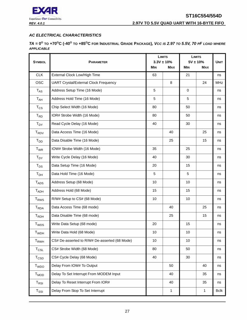
AC ELECTRICAL CHARACTERISTICS
TA = 0O TO +70OC (-40O TO +85OC FOR INDUSTRIAL GRADE PACKAGE), VCC IS 2.97 TO 5.5V, 70 PF LOAD WHERE APPLICABLE
SYMBOL PARAMETER
LIMITS
3.3V ± 10%MIN MAX
LIMITS
5V ± 10%MIN MAX
UNIT
CLK External Clock Low/High Time 63 21 ns
OSC UART Crystal/External Clock Frequency 8 24 MHz
TAS Address Setup Time (16 Mode) 5 0 ns
TAH Address Hold Time (16 Mode) 5 5 ns
TCS Chip Select Width (16 Mode) 80 50 ns
TRD IOR# Strobe Width (16 Mode) 80 50 ns
TDY Read Cycle Delay (16 Mode) 40 30 ns
TRDV Data Access Time (16 Mode) 40 25 ns
TDD Data Disable Time (16 Mode) 25 15 ns
TWR IOW# Strobe Width (16 Mode) 35 25 ns
TDY Write Cycle Delay (16 Mode) 40 30 ns
TDS Data Setup Time (16 Mode) 20 15 ns
TDH Data Hold Time (16 Mode) 5 5 ns
TADS Address Setup (68 Mode) 10 10 ns
TADH Address Hold (68 Mode) 15 15 ns
TRWS R/W# Setup to CS# (68 Mode) 10 10 ns
TRDA Data Access Time (68 mode) 40 25 ns
TRDH Data Disable Time (68 mode) 25 15 ns
TWDS Write Data Setup (68 mode) 20 15 ns
TWDH Write Data Hold (68 Mode) 10 10 ns
TRWH CS# De-asserted to R/W# De-asserted (68 Mode) 10 10 ns
TCSL CS# Strobe Width (68 Mode) 80 50 ns
TCSD CS# Cycle Delay (68 Mode) 40 30 ns
TWDO Delay From IOW# To Output 50 40 ns
TMOD Delay To Set Interrupt From MODEM Input 40 35 ns
TRSI Delay To Reset Interrupt From IOR# 40 35 ns
TSSI Delay From Stop To Set Interrupt 1 1 Bclk
27

ST16C554/554D 2.97V TO 5.5V QUAD UART WITH 16-BYTE FIFO REV. 4.0.1
TRRI Delay From IOR# To Reset Interrupt 45 40 ns
TSI Delay From Start To Interrupt 45 40 ns
TINT Delay From Initial INT Reset To Transmit Start 8 24 8 24 Bclk
TWRI Delay From IOW# To Reset Interrupt 45 40 ns
TSSR Delay From Stop To Set RXRDY# 1 1 Bclk
TRR Delay From IOR# To Reset RXRDY# 45 40 ns
TWT Delay From IOW# To Set TXRDY# 45 40 ns
TSRT Delay From Center of Start To Reset TXRDY# 8 8 Bclk
TRST Reset Pulse Width 40 40 ns
N Baud Rate Divisor 1 216-1 1 216-1 -
Bclk Baud Clock 16X of data rate Hz
FIGURE 11. CLOCK TIMING
AC ELECTRICAL CHARACTERISTICS
TA = 0O TO +70OC (-40O TO +85OC FOR INDUSTRIAL GRADE PACKAGE), VCC IS 2.97 TO 5.5V, 70 PF LOAD WHERE APPLICABLE
SYMBOL PARAMETER
LIMITS
3.3V ± 10%MIN MAX
LIMITS
5V ± 10%MIN MAX
UNIT
OSC
CLKCLK
EXTERNALCLOCK
28

ST16C554/554DREV. 4.0.1 2.97V TO 5.5V QUAD UART WITH 16-BYTE FIFO
FIGURE 12. MODEM INPUT/OUTPUT TIMING FOR CHANNELS A-D
FIGURE 13. 16 MODE (INTEL) DATA BUS READ TIMING FOR CHANNELS A-D
IO W #IO W
R T S #D T R #
C D #C T S #D S R #
IN T
IO R #
R I#
T W D O
T M O D T M O D
T R S I
T M O D
A c t iv e
A c t iv e
C h a n g e o f s ta te C h a n g e o f s ta te
A c t iv e A c t iv e A c t iv e
C h a n g e o f s ta te C h a n g e o f s ta te
C h a n g e o f s ta te
A c t iv e A c t iv e
TAS
TDD
TAH
TRD
TRDV
TDY
TDDTRDV
TAH
TAS
TCS
Valid Address Valid Address
Valid Data Valid Data
A0-A7
CS#
IOR#
D0-D7
RDTm
TCS
TRD
29

ST16C554/554D 2.97V TO 5.5V QUAD UART WITH 16-BYTE FIFO REV. 4.0.1
FIGURE 14. 16 MODE (INTEL) DATA BUS WRITE TIMING FOR CHANNELS A-D
FIGURE 15. 68 MODE (MOTOROLA) DATA BUS READ TIMING FOR CHANNELS A-D
16Write
TAS
TDH
TAH
TWR
TDS
TDY
TDHTDS
TAH
TAS
TCS
Valid Address Valid Address
Valid Data Valid Data
A0-A7
CS#
IOW#
D0-D7
TCS
TWR
68Read
TADS
TRDH
TADHTCSL
TRDA
TCSDTRWS
Valid Address Valid Address
Valid Data
A0-A7
CS#
R/W#
D0-D7
TRWH
Valid Data
30

ST16C554/554DREV. 4.0.1 2.97V TO 5.5V QUAD UART WITH 16-BYTE FIFO
FIGURE 16. 68 MODE (MOTOROLA) DATA BUS WRITE TIMING FOR CHANNELS A-D
FIGURE 17. RECEIVE READY & INTERRUPT TIMING [NON-FIFO MODE] FOR CHANNELS A-D
68Write
TADSTADHTCSL
TWDS
TCSDTRWS
Valid Address Valid Address
Valid Data
A0-A7
CS#
R/W#
D0-D7
TRWH
Valid Data
TWDH
RX
RXRDY#
IOR#
INT
D0:D7StartBit D0:D7
StopBit D0:D7
TSSR
1 Bytein RHR
ActiveData
Ready
ActiveData
Ready
ActiveData
Ready
1 Bytein RHR
1 Bytein RHR
TSSR TSSR
RXNFM
TRR TRR TRR
TSSR TSSR TSSR
(Reading dataout of RHR)
31

ST16C554/554D 2.97V TO 5.5V QUAD UART WITH 16-BYTE FIFO REV. 4.0.1
FIGURE 18. TRANSMIT READY & INTERRUPT TIMING [NON-FIFO MODE] FOR CHANNELS A-D
FIGURE 19. RECEIVE READY & INTERRUPT TIMING [FIFO MODE, DMA DISABLED] FOR CHANNELS A-D
TX
TXRDY#
IOW#
INT*
D0:D7StartBit D0:D7
StopBit D0:D7
TWT
TXNonFIFO
TWT TWT
TWRI TWRI TWRI
TSRT TSRT TSRT
*INT is cleared when the ISR is read or when data is loaded into the THR.
ISR is read ISR is readISR is read
(Loading datainto THR)
(Unloading)
IER[1]enabled
RX
RXRDY#
IOR#
INT
D0:D7S
TSSR
RXINTDMA#
RX FIFO fills up to RXTrigger Level or RX Data
Timeout
RX FIFO dropsbelow RX
Trigger Level
FIFOEmpties
First Byte isReceived in
RX FIFO
D0:D7S D0:D7T D0:D7S D0:D7ST D0:D7ST T D0:D7S T
StartBit
StopBit
TRRTRRI
TSSI
(Reading data outof RX FIFO)
32

ST16C554/554DREV. 4.0.1 2.97V TO 5.5V QUAD UART WITH 16-BYTE FIFO
FIGURE 20. RECEIVE READY & INTERRUPT TIMING [FIFO MODE, DMA ENABLED] FOR CHANNELS A-D
FIGURE 21. TRANSMIT READY & INTERRUPT TIMING [FIFO MODE, DMA MODE DISABLED] FOR CHANNELS A-D
RX
RXRDY#
IOR#
INT
D0:D7S
TSSR
RXFIFODMA
RX FIFO fills up to RXTrigger Level or RX Data
Timeout
RX FIFO dropsbelow RX
Trigger Level
FIFOEmpties
D0:D7S D0:D7T D0:D7S D0:D7ST D0:D7ST T D0:D7S T
StartBit
StopBit
TRRTRRI
TSSI
(Reading data outof RX FIFO)
TX
TXRDY#
IOW#
INT*
D0:D7S D0:D7T D0:D7S D0:D7ST D0:D7ST T D0:D7S T
StartBit
StopBit
(Unloading)
(Loading datainto FIFO)
Last Data ByteTransmitted
Data inTX FIFO
TX FIFOEmpty
TWT
TSI
TX FIFOEmpty
TTS
ISR is readIER[1]enabled
ISR is read
*INT is cleared when the ISR is read or when at least 1 byte is written to the TX FIFO.
TWRI
33

ST16C554/554D 2.97V TO 5.5V QUAD UART WITH 16-BYTE FIFO REV. 4.0.1
FIGURE 22. TRANSMIT READY & INTERRUPT TIMING [FIFO MODE, DMA MODE ENABLED] FOR CHANNELS A-D
TX
TXRDY#
IOW#
INT*
D0:D7S D0:D7T D0:D7S D0:D7ST D0:D7ST T D0:D7S T
StartBit
StopBit
(Unloading)
(Loading datainto FIFO)
Last Data ByteTransmitted
TSI
TX FIFOEmpty
TTS
ISR is readIER[1]enabled
ISR is read
*INT is cleared when the ISR is read or when at least 1 byte is written to the TX FIFO.
TWRI
At least 1empty location
in FIFO
TSRT
TX FIFOFull
TWT
34
ST16C554/554DREV. 4.0.1 2.97V TO 5.5V QUAD UART WITH 16-BYTE FIFO
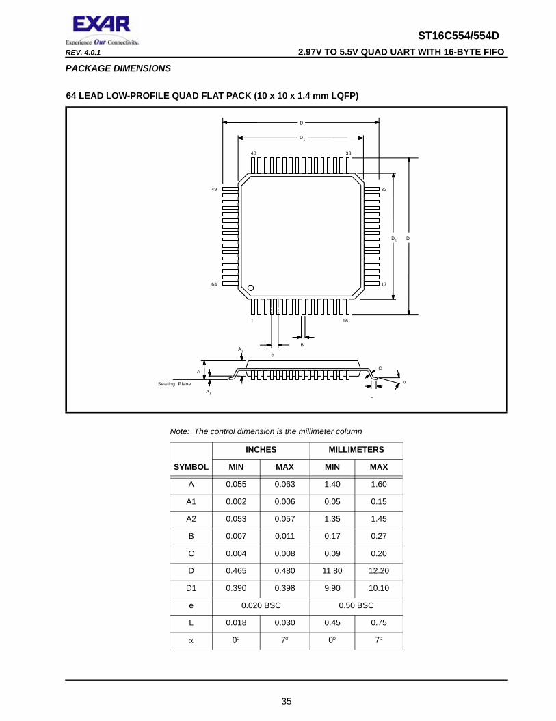
PACKAGE DIMENSIONS
64 LEAD LOW-PROFILE QUAD FLAT PACK (10 x 10 x 1.4 mm LQFP)
Note: The control dimension is the millimeter column
INCHES MILLIMETERS
SYMBOL MIN MAX MIN MAX
A 0.055 0.063 1.40 1.60
A1 0.002 0.006 0.05 0.15
A2 0.053 0.057 1.35 1.45
B 0.007 0.011 0.17 0.27
C 0.004 0.008 0.09 0.20
D 0.465 0.480 11.80 12.20
D1 0.390 0.398 9.90 10.10
e 0.020 BSC 0.50 BSC
L 0.018 0.030 0.45 0.75
α 0° 7° 0° 7°
48 33
32
17
1 16
49
64
D
D1
DD1
B
eA2
α
A1
A
Seating Plane
L
C
35

ST16C554/554D 2.97V TO 5.5V QUAD UART WITH 16-BYTE FIFO REV. 4.0.1
68 LEAD PLASTIC LEADED CHIP CARRIER (PLCC)
Note: The control dimension is the inch column
INCHES MILLIMETERS
SYMBOL MIN MAX MIN MAX
A 0.165 0.200 4.19 5.08
A1 0.090 0.130 2.29 3.30
A2 0.020 ---. 0.51 ---
B 0.013 0.021 0.33 0.53
B1 0.026 0.032 0.66 0.81
C 0.008 0.013 0.19 0.32
D 0.985 0.995 25.02 25.27
D1 0.950 0.958 24.13 24.33
D2 0.890 0.930 22.61 23.62
D3 0.800 typ. 20.32 typ.
e 0.050 BSC 1.27 BSC
H1 0.042 0.056 1.07 1.42
H2 0.042 0.048 1.07 1.22
R 0.025 0.045 0.64 1.14
1
D
D1
D D1
D3
D2
A
A1
2 68
B
A2
B1
e
Seating Plane
D3
45° x H2
45° x H1
C
R
36

ST16C554/554DREV. 4.0.1 2.97V TO 5.5V QUAD UART WITH 16-BYTE FIFO
REVISION HISTORY
DATE REVISION DESCRIPTION
August 2004 3.3.0 Added Revision History and Device Status.
August 2005 3.3.1 Updated the 1.4mm-thick Quad Flat Pack package description from "TQFP" to "LQFP" to be consistent with JEDEC and Industry norms.
April 2006 4.0.0 New datasheet format. Changed active low signal designator from "-" in front of sig-nal name to "#" after signal name. Updated AC Electrical Characteristics.
June 2006 4.0.1 Corrected Part Numbers in Ordering Information.
37
NOTICE
EXAR Corporation reserves the right to make changes to the products contained in this publication in order to improve design, performance or reliability. EXAR Corporation assumes no responsibility for the use of any circuits described herein, conveys no license under any patent or other right, and makes no representation that the circuits are free of patent infringement. Charts and schedules contained here in are only for illustration purposes and may vary depending upon a user’s specific application. While the information in this publication has been carefully checked; no responsibility, however, is assumed for inaccuracies.
EXAR Corporation does not recommend the use of any of its products in life support applications where the failure or malfunction of the product can reasonably be expected to cause failure of the life support system or to significantly affect its safety or effectiveness. Products are not authorized for use in such applications unless EXAR Corporation receives, in writing, assurances to its satisfaction that: (a) the risk of injury or damage has been minimized; (b) the user assumes all such risks; (c) potential liability of EXAR Corporation is adequately protected under the circumstances.
Copyright 2006 EXAR Corporation
Datasheet June 2006.
Send your UART technical inquiry with technical details to hotline: [email protected].
Reproduction, in part or whole, without the prior written consent of EXAR Corporation is prohibited.

ST16C554/554D 2.97V TO 5.5V QUAD UART WITH 16-BYTE FIFO REV. 4.0.1
TABLE OF CONTENTS
GENERAL DESCRIPTION ................................................................................................ 1FEATURES .................................................................................................................................................... 1APPLICATIONS............................................................................................................................................... 1
FIGURE 1. ST16C554 BLOCK DIAGRAM ........................................................................................................................................... 1FIGURE 2. PIN OUT ASSIGNMENT ..................................................................................................................................................... 2
ORDERING INFORMATION................................................................................................................................ 2PIN DESCRIPTIONS ........................................................................................................ 31.0 PRODUCT DESCRIPTION....................................................................................................................... 62.0 FUNCTIONAL DESCRIPTIONS............................................................................................................... 7
2.1 CPU INTERFACE................................................................................................................................................. 7FIGURE 3. ST16C554 TYPICAL INTEL/MOTOROLA DATA BUS INTERCONNECTIONS............................................................................. 7
2.2 DEVICE RESET ................................................................................................................................................... 82.3 CHANNEL SELECTION....................................................................................................................................... 8
TABLE 1: CHANNEL A-D SELECT IN 16 MODE ................................................................................................................................... 8TABLE 2: CHANNEL A-D SELECT IN 68 MODE ................................................................................................................................... 8
2.4 CHANNELS A-D INTERNAL REGISTERS ......................................................................................................... 92.5 INT OUPUTS FOR CHANNELS A-D................................................................................................................... 9
TABLE 3: INT PIN OPERATION FOR TRANSMITTER FOR CHANNELS A-D ............................................................................................. 9TABLE 4: INT PIN OPERATION FOR RECEIVER FOR CHANNELS A-D ................................................................................................... 9
2.6 DMA MODE.......................................................................................................................................................... 9TABLE 5: TXRDY# AND RXRDY# OUTPUTS IN FIFO AND DMA MODE FOR CHANNELS A-D ........................................................... 10
2.7 CRYSTAL OSCILLATOR OR EXTERNAL CLOCK INPUT.............................................................................. 10FIGURE 4. TYPICAL CRYSTAL CONNECTIONS................................................................................................................................... 10
2.8 PROGRAMMABLE BAUD RATE GENERATOR.............................................................................................. 10FIGURE 5. BAUD RATE GENERATOR ............................................................................................................................................... 11TABLE 6: TYPICAL DATA RATES WITH A 14.7456 MHZ CRYSTAL OR EXTERNAL CLOCK ...................................................................... 11
2.9 TRANSMITTER.................................................................................................................................................. 112.9.1 TRANSMIT HOLDING REGISTER (THR) - WRITE ONLY........................................................................................... 112.9.2 TRANSMITTER OPERATION IN NON-FIFO MODE .................................................................................................... 12
FIGURE 6. TRANSMITTER OPERATION IN NON-FIFO MODE .............................................................................................................. 122.9.3 TRANSMITTER OPERATION IN FIFO MODE ............................................................................................................. 12
FIGURE 7. TRANSMITTER OPERATION IN FIFO MODE...................................................................................................................... 122.10 RECEIVER ....................................................................................................................................................... 12
2.10.1 RECEIVE HOLDING REGISTER (RHR) - READ-ONLY ............................................................................................ 13FIGURE 8. RECEIVER OPERATION IN NON-FIFO MODE.................................................................................................................... 13FIGURE 9. RECEIVER OPERATION IN FIFO...................................................................................................................................... 13
2.11 INTERNAL LOOPBACK................................................................................................................................. 14FIGURE 10. INTERNAL LOOP BACK IN CHANNEL A AND B ................................................................................................................ 14
3.0 UART INTERNAL REGISTERS ............................................................................................................. 15TABLE 7: UART CHANNEL A AND B UART INTERNAL REGISTERS ...................................................................................... 15TABLE 8: INTERNAL REGISTERS DESCRIPTION. .................................................................................................................. 16
4.0 INTERNAL REGISTER DESCRIPTIONS............................................................................................... 164.1 RECEIVE HOLDING REGISTER (RHR) - READ- ONLY .................................................................................. 164.2 TRANSMIT HOLDING REGISTER (THR) - WRITE-ONLY ............................................................................... 164.3 INTERRUPT ENABLE REGISTER (IER) - READ/WRITE................................................................................. 16
4.3.1 IER VERSUS RECEIVE FIFO INTERRUPT MODE OPERATION ............................................................................... 174.3.2 IER VERSUS RECEIVE/TRANSMIT FIFO POLLED MODE OPERATION.................................................................. 17
4.4 INTERRUPT STATUS REGISTER (ISR) ........................................................................................................... 184.4.1 INTERRUPT GENERATION: ........................................................................................................................................ 184.4.2 INTERRUPT CLEARING: ............................................................................................................................................. 18
TABLE 9: INTERRUPT SOURCE AND PRIORITY LEVEL ....................................................................................................................... 184.5 FIFO CONTROL REGISTER (FCR) - WRITE-ONLY......................................................................................... 19
TABLE 10: RECEIVE FIFO TRIGGER LEVEL SELECTION ................................................................................................................... 194.6 LINE CONTROL REGISTER (LCR) - READ/WRITE......................................................................................... 20
TABLE 11: PARITY SELECTION ........................................................................................................................................................ 214.7 MODEM CONTROL REGISTER (MCR) OR GENERAL PURPOSE OUTPUTS CONTROL - READ/WRITE.. 21
TABLE 12: INT OUTPUT MODES ..................................................................................................................................................... 224.8 LINE STATUS REGISTER (LSR) - READ/WRITE ............................................................................................ 224.9 MODEM STATUS REGISTER (MSR) - READ/WRITE...................................................................................... 23
I

ST16C554/554DREV. 4.0.1 2.97V TO 5.5V QUAD UART WITH 16-BYTE FIFO
4.10 SCRATCH PAD REGISTER (SPR) - READ/WRITE ....................................................................................... 244.11 BAUD RATE GENERATOR REGISTERS (DLL AND DLM) - READ/WRITE................................................. 24
TABLE 13: UART RESET CONDITIONS FOR CHANNELS A-D ................................................................................................. 25ABSOLUTE MAXIMUM RATINGS ................................................................................. 26TYPICAL PACKAGE THERMAL RESISTANCE DATA (MARGIN OF ERROR: ± 15%) 26ELECTRICAL CHARACTERISTICS............................................................................... 26
DC ELECTRICAL CHARACTERISTICS............................................................................................................. 26AC ELECTRICAL CHARACTERISTICS............................................................................................................. 27TA = 0O TO +70OC (-40O TO +85OC FOR INDUSTRIAL GRADE PACKAGE), VCC IS 2.97 TO 5.5V, 70 PF LOAD WHERE APPLICABLE ................................................................................................................................................ 27
FIGURE 11. CLOCK TIMING............................................................................................................................................................. 28FIGURE 12. MODEM INPUT/OUTPUT TIMING FOR CHANNELS A-D .................................................................................................... 29FIGURE 13. 16 MODE (INTEL) DATA BUS READ TIMING FOR CHANNELS A-D ................................................................................... 29FIGURE 14. 16 MODE (INTEL) DATA BUS WRITE TIMING FOR CHANNELS A-D.................................................................................. 30FIGURE 15. 68 MODE (MOTOROLA) DATA BUS READ TIMING FOR CHANNELS A-D........................................................................... 30FIGURE 17. RECEIVE READY & INTERRUPT TIMING [NON-FIFO MODE] FOR CHANNELS A-D ............................................................ 31FIGURE 16. 68 MODE (MOTOROLA) DATA BUS WRITE TIMING FOR CHANNELS A-D ......................................................................... 31FIGURE 18. TRANSMIT READY & INTERRUPT TIMING [NON-FIFO MODE] FOR CHANNELS A-D .......................................................... 32FIGURE 19. RECEIVE READY & INTERRUPT TIMING [FIFO MODE, DMA DISABLED] FOR CHANNELS A-D........................................... 32FIGURE 20. RECEIVE READY & INTERRUPT TIMING [FIFO MODE, DMA ENABLED] FOR CHANNELS A-D............................................ 33FIGURE 21. TRANSMIT READY & INTERRUPT TIMING [FIFO MODE, DMA MODE DISABLED] FOR CHANNELS A-D .............................. 33FIGURE 22. TRANSMIT READY & INTERRUPT TIMING [FIFO MODE, DMA MODE ENABLED] FOR CHANNELS A-D ............................... 34
PACKAGE DIMENSIONS................................................................................................................................ 35REVISION HISTORY ..................................................................................................................................... 37
TABLE OF CONTENTS ..................................................................................................... I
II