ssntd ion track technology to nanotechnology
TRANSCRIPT
My Journey from Ion Track Technology to Nanotechnology
Hardev Singh VirkProfessor Emeritus
Eternal University, Baru Sahib,HP, India
History of Nuclear Tracks
Rutherford’s discovery Alpha tracks:1906(Wilson Cloud chamber used as a detector)
Ruchi Ram Sahni studied Alpha tracks in Nuclear Emulsion in Rutherford Lab.1915
Discovery of Pi Mesons by C.F. Powel using Nuclear Emulsions in Bristol 1940s
Beva Chowdhary used N. Emulsions for study of Pi mesons in Calcutta University.
D.Lal, Y.Pal & B.Peters in TIFR used NE:1950s

Routes to Nanotechnology
• Physical, chemical, biological and nature’s self assembly.
• Top-down and bottom-up approaches.• Chemical route to nanotechnology is simpler,
cheaper and allows fabrication at bench top conditions.
• Reverse micelles (microemulsions route) is a versatile method to produce a variety of nanoparticles.
My Route to Nanotechnology
• Ion Track Technology Route using Heavy Ion Beams from GSI, Darmstadt & JINR, Dubna.
• Chemical Route of Reverse micelles, co-precipitation, solvo-thermal, sol-gel and seed growth techniques.
• Quantum dots, nanorods and nanoneedles of Barium Carbonate, Barium Oxalate, Iron Oxalate, Barium hexaferrite, Zinc Oxide, Cadmium Sulphide, Cadmium Oxide and Silver prepared.

Ion Track Technology Ion Track Technology
Ion Track Technology [1] was developed at GSI, Ion Track Technology [1] was developed at GSI, Darmstadt. Ion Track Filters (ITFs) or Track-etched Darmstadt. Ion Track Filters (ITFs) or Track-etched membranes became precursors to development of membranes became precursors to development of nanotechnology during 1990s. ITFs were prepared nanotechnology during 1990s. ITFs were prepared by bombardment of thin polymer foils using heavy by bombardment of thin polymer foils using heavy ions. One of the first applications of ITFs was ions. One of the first applications of ITFs was separation of cancer blood cells from normal blood separation of cancer blood cells from normal blood by making use of Nuclepore filters. Author’s group by making use of Nuclepore filters. Author’s group used heavy ion beam facility available at GSI used heavy ion beam facility available at GSI UNILAC, Darmstadt during 1980s for Ion Beam UNILAC, Darmstadt during 1980s for Ion Beam Modification of Materials and to prepare ITFs in our Modification of Materials and to prepare ITFs in our laboratory. laboratory.
[1] R. Spohr: [1] R. Spohr: Ion Tracks and Microtechnology: Principles and Applications Ion Tracks and Microtechnology: Principles and Applications (Vieweg Publications, Weisbaden Germany, 1990) (Vieweg Publications, Weisbaden Germany, 1990)
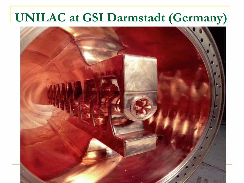
UNILAC at GSI Darmstadt (Germany)
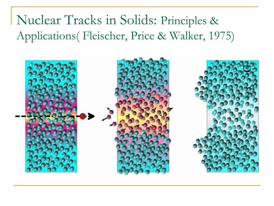
Nuclear Tracks in Solids: Principles & Applications( Fleischer, Price & Walker, 1975)

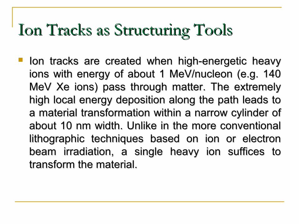
Ion Tracks as Structuring Tools Ion Tracks as Structuring Tools
Ion tracks are created when high-energetic heavy Ion tracks are created when high-energetic heavy ions with energy of about 1 MeV/nucleon (e.g. 140 ions with energy of about 1 MeV/nucleon (e.g. 140 MeV Xe ions) pass through matter. The extremely MeV Xe ions) pass through matter. The extremely high local energy deposition along the path leads to high local energy deposition along the path leads to a material transformation within a narrow cylinder of a material transformation within a narrow cylinder of about 10 nm width. Unlike in the more conventional about 10 nm width. Unlike in the more conventional lithographic techniques based on ion or electron lithographic techniques based on ion or electron beam irradiation, a single heavy ion suffices to beam irradiation, a single heavy ion suffices to transform the material. transform the material.
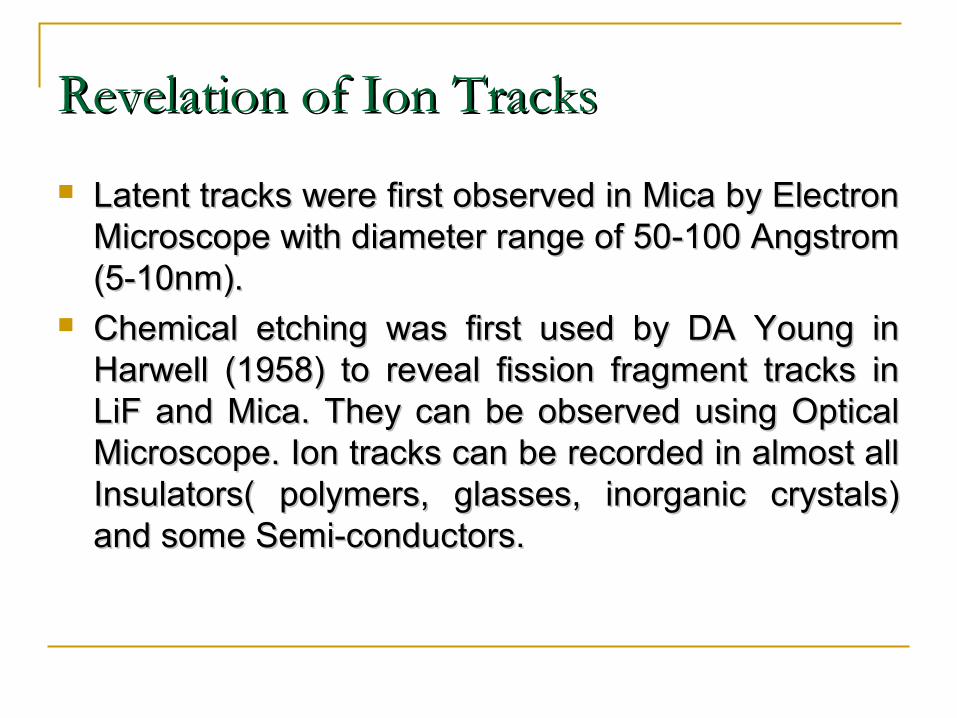
Revelation of Ion TracksRevelation of Ion Tracks
Latent tracks were first observed in Mica by Electron Latent tracks were first observed in Mica by Electron Microscope with diameter range of 50-100 Angstrom Microscope with diameter range of 50-100 Angstrom (5-10nm).(5-10nm).
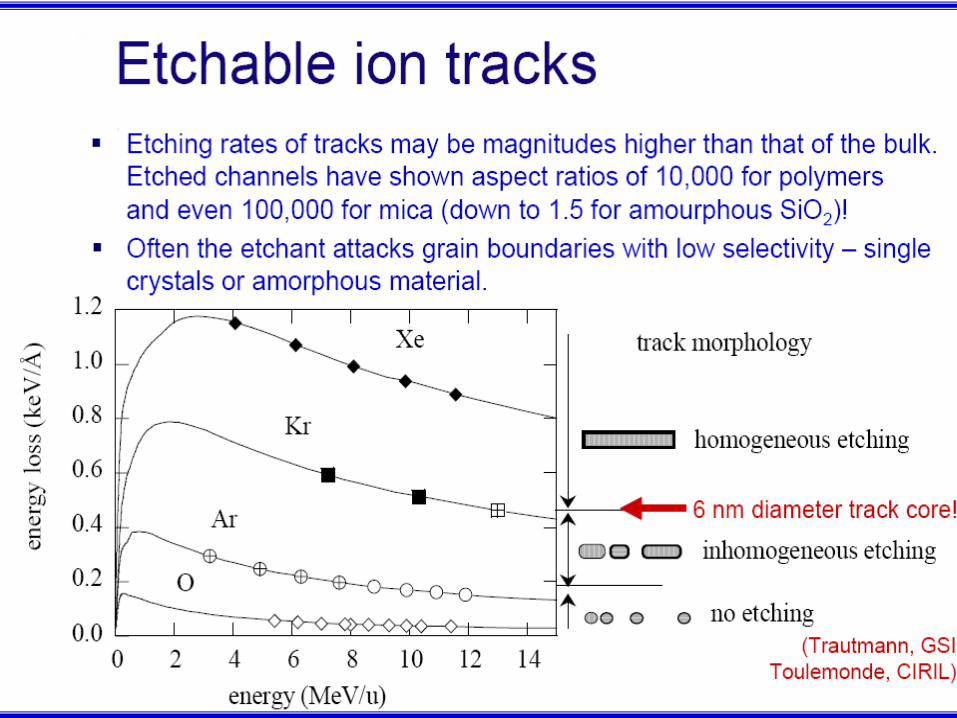
Chemical etching was first used by DA Young in Chemical etching was first used by DA Young in Harwell (1958) to reveal fission fragment tracks in Harwell (1958) to reveal fission fragment tracks in LiF and Mica. They can be observed using Optical LiF and Mica. They can be observed using Optical Microscope. Ion tracks can be recorded in almost all Microscope. Ion tracks can be recorded in almost all Insulators( polymers, glasses, inorganic crystals) Insulators( polymers, glasses, inorganic crystals) and some Semi-conductors.and some Semi-conductors.

Latent Pb-Ion Tracks in MicaLatent Pb-Ion Tracks in Mica
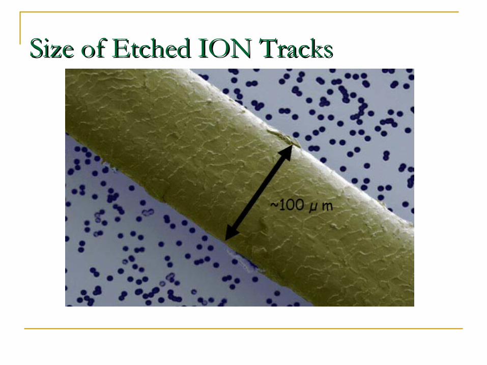
Size of Etched ION TracksSize of Etched ION Tracks
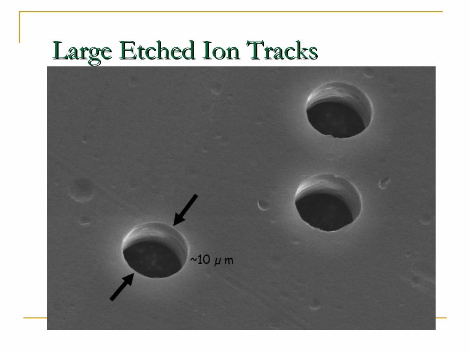
Large Etched Ion TracksLarge Etched Ion Tracks
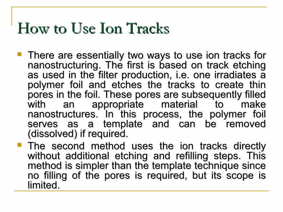
How to Use Ion TracksHow to Use Ion Tracks
There are essentially two ways to use ion tracks for There are essentially two ways to use ion tracks for nanostructuring. The first is based on track etching nanostructuring. The first is based on track etching as used in the filter production, i.e. one irradiates a as used in the filter production, i.e. one irradiates a polymer foil and etches the tracks to create thin polymer foil and etches the tracks to create thin pores in the foil. These pores are subsequently filled pores in the foil. These pores are subsequently filled with an appropriate material to make with an appropriate material to make nanostructures. In this process, the polymer foil nanostructures. In this process, the polymer foil serves as a template and can be removed serves as a template and can be removed (dissolved) if required.(dissolved) if required.
The second method uses the ion tracks directly The second method uses the ion tracks directly without additional etching and refilling steps. This without additional etching and refilling steps. This method is simpler than the template technique since method is simpler than the template technique since no filling of the pores is required, but its scope is no filling of the pores is required, but its scope is limited. limited.

Nanowire Fabrication
Template synthesis using polymer and anodic alumina membranes
Electrochemical deposition Ensures fabrication of electrically continuous wires
since it only takes place on conductive surfaces Applicable to a wide range of materials
High pressure injection Limited to elements and heterogeneously-melting
compounds with low melting points Does not ensure continuous wires Does not work well for diameters < 30-40 nm
Chemical Vapor Deposition (CVD) or VLS technique Laser assisted techniques

Polymer Template Synthesis of Nanowires
(T. Sands/ HEMI group http://www.mse.berkeley.edu/groups/Sands/HEMI/nanoTE.html)
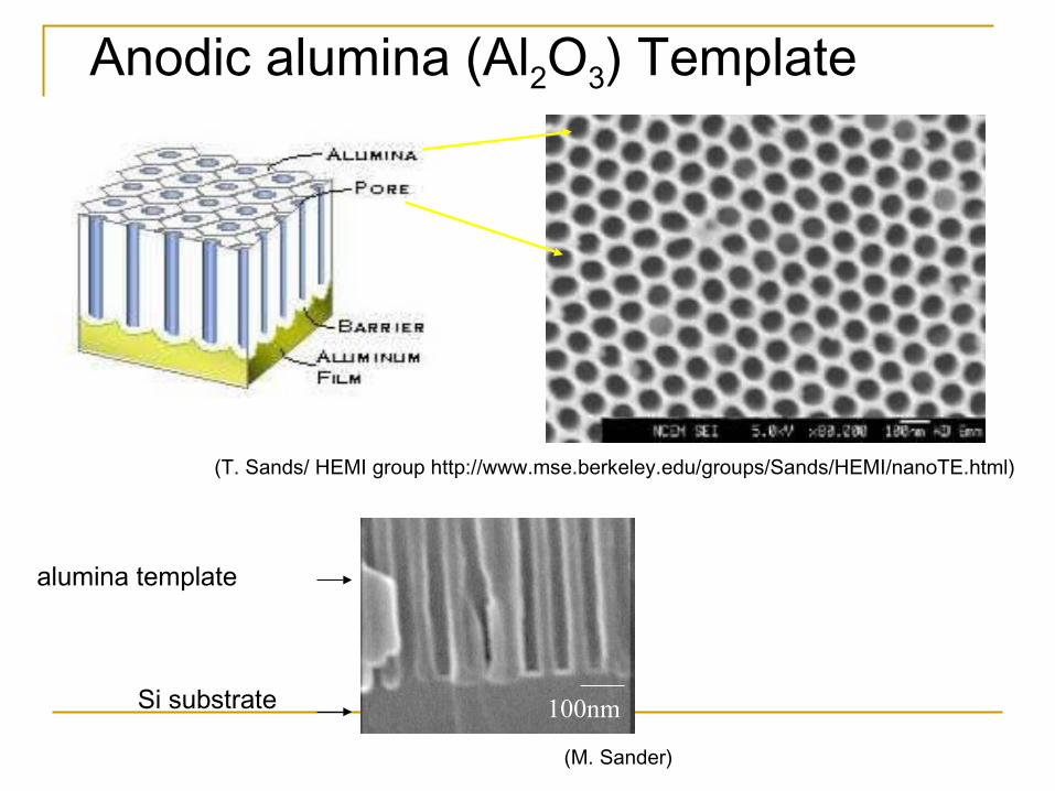
Anodic alumina (Al2O3) Template
100nmSi substrate
alumina template
(M. Sander)

Electrolytic CellElectrolytic Cell

Template Synthesis of Copper NanowiresTemplate Synthesis of Copper Nanowires
The concept of electro-deposition of metals through The concept of electro-deposition of metals through electroplating is described as an electrochemical electroplating is described as an electrochemical process. The etched pores of ITFs used would act process. The etched pores of ITFs used would act as a template. The electrolyte used here was as a template. The electrolyte used here was CuSO4.5H2O acidic solution. The rate of deposition CuSO4.5H2O acidic solution. The rate of deposition of metallic film depends upon many factors, i.e., of metallic film depends upon many factors, i.e., current density, inter-electrode distance, cell current density, inter-electrode distance, cell voltage, electrolyte concentration and temperature voltage, electrolyte concentration and temperature etc. In the present set up electrode distance was etc. In the present set up electrode distance was kept 0.5 cm and a current of 0.0025A was applied kept 0.5 cm and a current of 0.0025A was applied for 50 minutes. The developed microstructures for 50 minutes. The developed microstructures were scanned under SEM (Jeol, JSM-6100) for were scanned under SEM (Jeol, JSM-6100) for morphological and structural studies.morphological and structural studies.
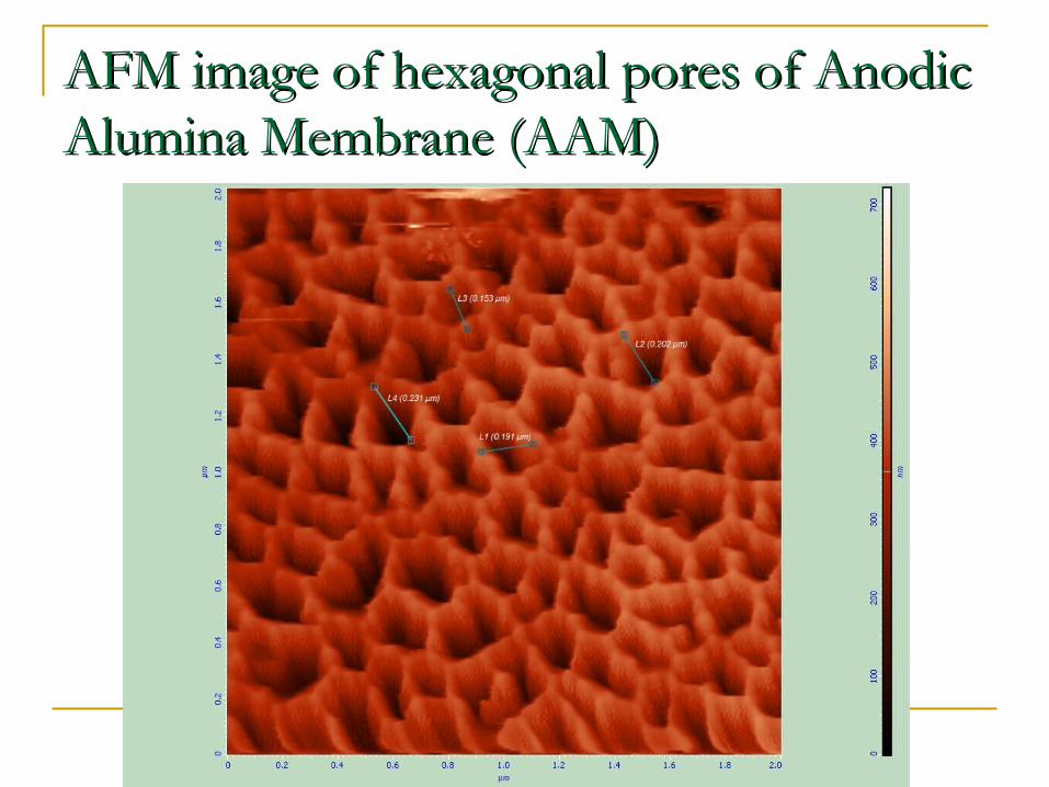
AFM image of hexagonal pores of Anodic AFM image of hexagonal pores of Anodic Alumina Membrane (AAM)Alumina Membrane (AAM)

SEM Images of Cu Nanowires using SEM Images of Cu Nanowires using Electrodeposition TechniqueElectrodeposition Technique
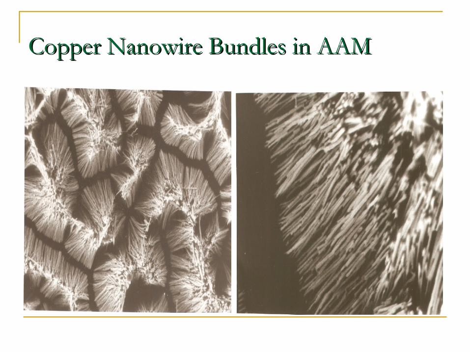
Copper Nanowire Bundles in AAMCopper Nanowire Bundles in AAM
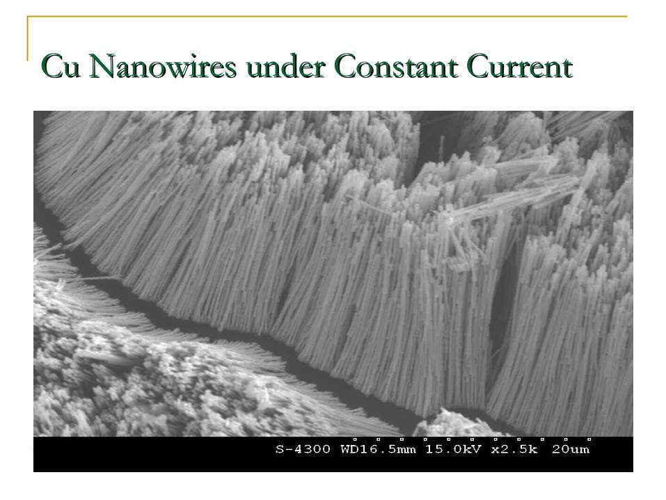
Cu Nanowires under Constant CurrentCu Nanowires under Constant Current
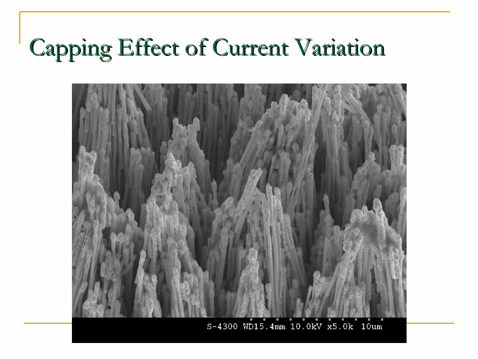
Capping Effect of Current VariationCapping Effect of Current Variation
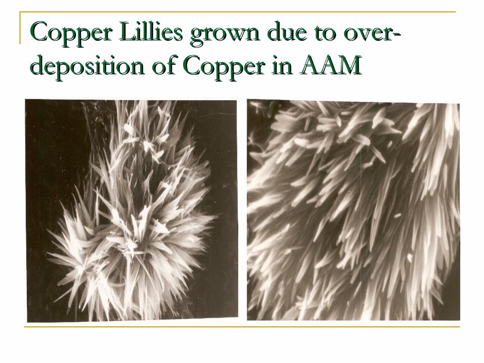
Copper Lillies grown due to over- Copper Lillies grown due to over- deposition of Copper in AAM deposition of Copper in AAM

Copper Nanoflowers grown in Polymer Template (100nm pores)
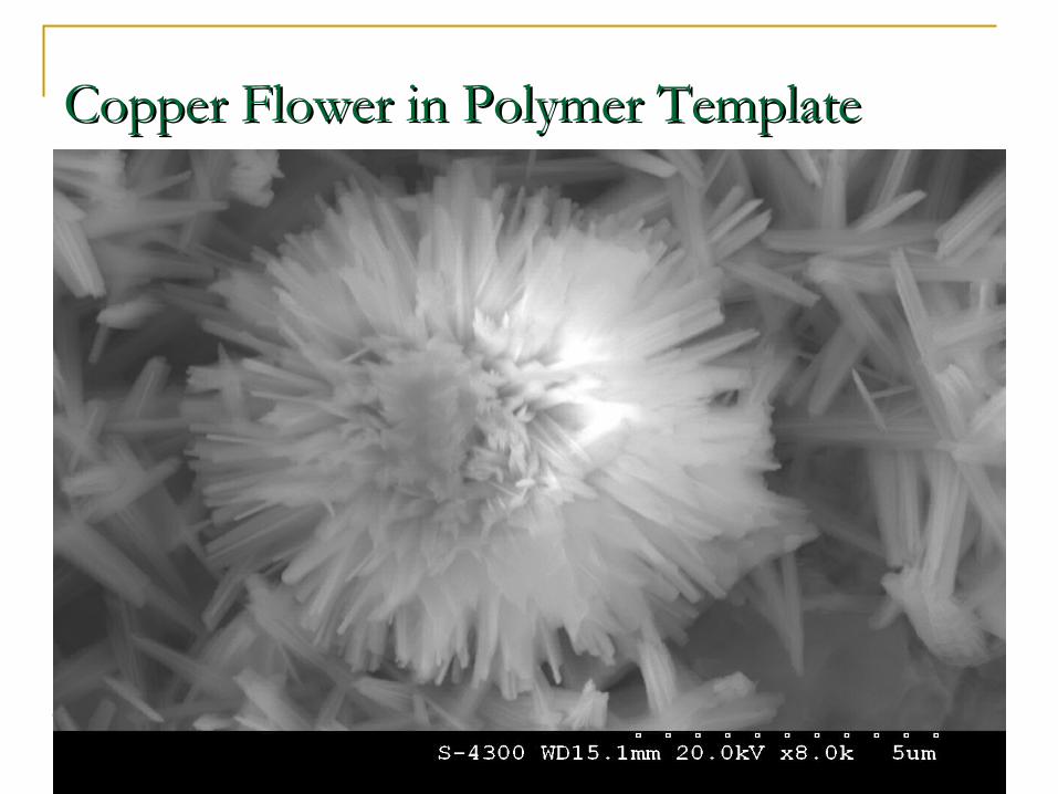
Copper Flower in Polymer Template Copper Flower in Polymer Template
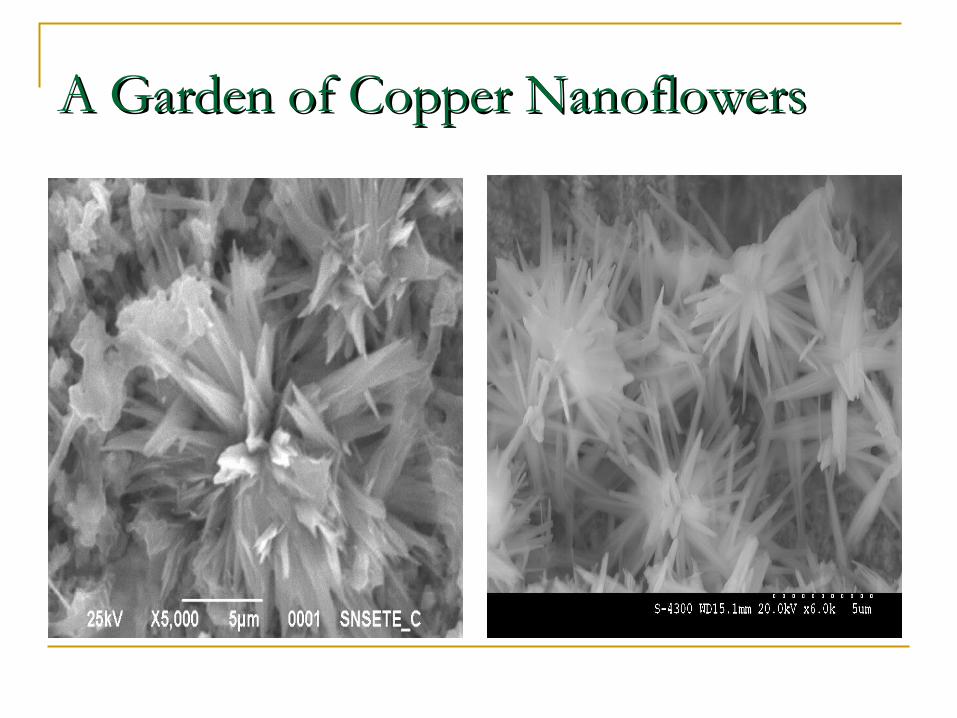
A Garden of Copper NanoflowersA Garden of Copper Nanoflowers

I-V Characteristics of Copper Nanowires I-V Characteristics of Copper Nanowires grown in-situ in AAMgrown in-situ in AAM
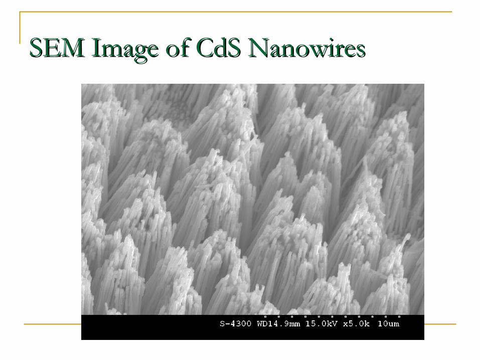
SEM Image of CdS NanowiresSEM Image of CdS Nanowires

HRTEM image showing CdS Nanowire & HRTEM image showing CdS Nanowire & Heterojunctions Heterojunctions

I-V plot of CdS Nanowire arrays showing I-V plot of CdS Nanowire arrays showing RTD characteristics RTD characteristics

SEM image of Cu-Se NanowiresSEM image of Cu-Se Nanowires

Cu-Se nanowires exhibit p-n junction Cu-Se nanowires exhibit p-n junction diode characteristicsdiode characteristics
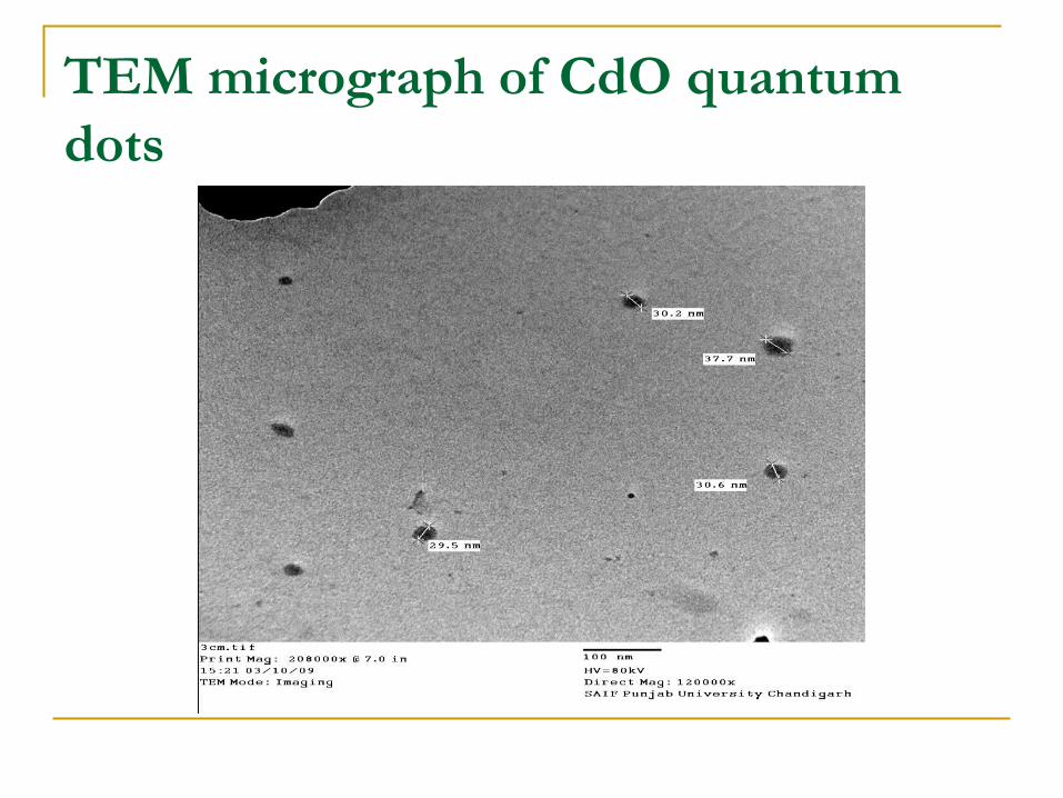
TEM micrograph of CdO quantum dots
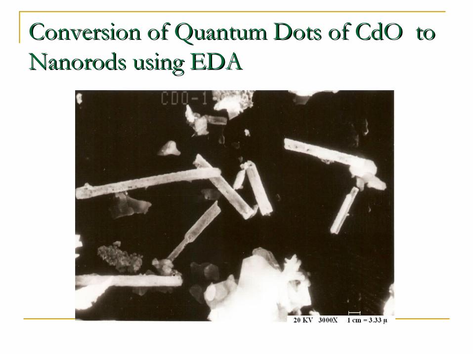
Conversion of Quantum Dots of CdO to Conversion of Quantum Dots of CdO to Nanorods using EDA Nanorods using EDA
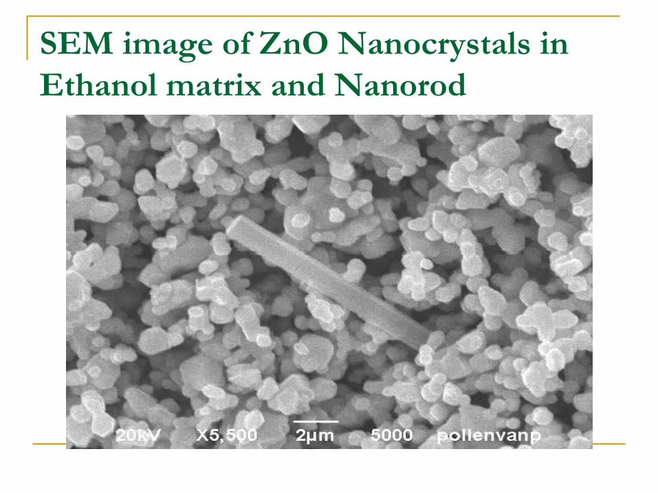
SEM image of ZnO Nanocrystals in Ethanol matrix and Nanorod
AcknowledgementsAcknowledgements
Reimer Spohr & Christina Trautman (GSI, Darmstadt)Reimer Spohr & Christina Trautman (GSI, Darmstadt) Sanjit Amrita Kaur (GND University, Amritsar)Sanjit Amrita Kaur (GND University, Amritsar) Vishal, Gurmit, Sehdev & KK (DAVIET, Jalandhar)Vishal, Gurmit, Sehdev & KK (DAVIET, Jalandhar) Dr SK Mehta, Chemistry Deptt. (PU, Chandigarh) Dr SK Mehta, Chemistry Deptt. (PU, Chandigarh) CSIO Chandigarh & IIT Roorkee for FESEM & TEM facility.CSIO Chandigarh & IIT Roorkee for FESEM & TEM facility. SEM & TEM facility (SAIF, PU, Chandigarh)SEM & TEM facility (SAIF, PU, Chandigarh) Rajeev Patnaik (Geology Deptt., PU, Chandigarh)Rajeev Patnaik (Geology Deptt., PU, Chandigarh) DAV MC, New Delhi for Research Grants.DAV MC, New Delhi for Research Grants. Dr. MS Atwal, VC, Eternal University, Baru Sahib.Dr. MS Atwal, VC, Eternal University, Baru Sahib.

Thank You !!!