spring-8-ii conceptual design report - rikenrsc.riken.jp/pdf/spring-8-ii.pdfspring-8-ii conceptual...
TRANSCRIPT

SPring-8-II
Conceptual Design Report
RIKEN SPring-8 Center
November, 2014

General Introduction

Seventeen years have passed since the 1997 inauguration of SPring-8 as the highest-electron-energy, large-scale third generation synchrotron radiation (SR) facility in the world. Since then, SPring-8 has been playing a leading role in high-energy photon science, welcoming around 170,000 users from both the academic and industrial sectors. It should be noted that no new SR facilities larger than SPring-8 have been built during this time. Instead, newer SR facilities have followed the model of lower-energy, medium-size electron storage rings with fairly low-emittance. This trend was kicked off by the research and development at SPring-8 for in-vacuum type undulators, which are able to reduce the magnetic period length of the undulators. SPring-8 employed in-vacuum undulators as standard insertion devices. In the earlier stages of the medium-sized facilities, we observed them managing to produce hard X-rays from undulators. But now, the performance of medium-sized facilities is about to surpass that of the older, large-scale facilities, owing to the past decade’s rapid technological progress. The newer technologies clearly have the potential to convert existing large-scale facilities into super-performance SR facilities. At the SPring-8 site, the first adaptation of newer technology was not in the storage ring, but in the X-ray free electron laser (XFEL). A shorter magnetic-period, in-vacuum undulator enabled us to implement a “compact” SASE (self-amplified spontaneous emission) XFEL. The first proposal for the compact SASE source was submitted in 2000, followed by an R&D phase from 2001 to 2005, and ending up with the construction of a prototype FEL operating in the extreme ultraviolet (EUV) region. This initiative was highlighted in the 3rd midterm “Basic Program for Science and Technology,” which designated the compact XFEL as one of the five “Key Technologies of National Importance”. The SACLA (SPring-8 Angstrom Compact Laser) project started accordingly in 2006 with a total budget of 40B JP¥ (approximately US$400M in 2014) and a 5-year schedule. We designed the SACLA linear accelerator (linac) to be used for a full-energy injector for
the SPring-8 storage ring. An ultra-low-emittance electron beam deliveredfrom the SACLA linac should be compatible with the future upgraded SPring-8 facility. SACLA completed the project on time and on budget. It is now in operation supporting user programs.
SACLA is delivering pulsed X-ray laser beams whose pulse duration is asshort as a few femtoseconds (10-15 second). The peak brilliance of the SASE FEL is so high that samples can be destroyed after a single shot irradiation of the SASE pulse. However, the extremely short pulse width enables us to extract sample information through scattering, absorption, photon or photoelectron emission before the sample is destroyed. This “measure before destroy” scheme is characteristic of FEL experiments. The scheme requires reconstructing the full data set from many independent data results taken from different samples as exemplified in serial femtosecond crystallography (SFX). This technique is a marked contrast to data taking with SR, which usually provides a full data set from measurement with a single sample. The complementary use of storage-ring light sources and XFELs is essential to opening new frontiers in science and technology, partly because XFELs allow access to ultra-fast time domains, which are inaccessible with storage ring sources. However, there is a wide gap between what the current SPring-8 can do and what SACLA can do. The SPring-8 upgrade to SPring-8-II should narrow the gap from the storage ring perspective. We expect the upgraded facility to offer lower emittance and a higher coherent flux. For many phenomena at the atomic scale, we know how they happen, but we do not know why they happen. The most important role of SPring-8-II, combined with SACLA, is the construction of the basic tool to provide the answers to the many “whys.” A joint design team for SPring-8-II was established in collaboration between RIKEN and JASRI. Dr. Hitoshi Tanaka, who is the Division Head of XFEL R&D, was nominated as the head of the design team. After several months of rigorous design work, we are pleased to publish the “Conceptual Design

Report (CDR).” PART-I provides an overview of the light source related design, including the accelerator, insertion devices, the control system, and radiation safety issues, while PART-II addresses scientific scope, beamline design, and end-station considerations. With this CDR, we would like to begin the review process with international experts. We hope to initiate the next step of the Engineering Design Process in 2015 FY. We welcome any feedback from machine experts and future users of the light source. We would like to inaugurate SPring-8-II in the early 2020s.
Tetsuya Ishikawa Director RIKEN SPring-8 Center

Table of Contents
PART-I: Light Source Development I-1 Accelerator Design………………………………..………. 1-97 I-2 Light Sources………………………………..……………... 98-133 I-3 Control System………………………………..…………...134-147 I-4 Safety Issues……………………………………..…………148-160
PART-II: Scientific Scope and Beamline Development II-1 Overview……………………………………..…………......161-165 II-2 Beamline Design………………………………………...166-190 II-3 Detector System………………………………………….191-199 Appendix

2
PART-I I-1 Accelerator Design
I-1.1. Overview I-1.2. Storage Ring Lattice I-1.3. Beam Dynamics Issues I-1.4. Magnet System I-1.5. Vacuum System I-1.6. RF System I-1.7. Beam Instrumentation and Instability Feedback I-1.8. Injector I-1.9. Storage Ring Lattice Data
2
I-1.1. Overview The following three factors led us to adopt more conservative, less
aggressive accelerator specifications compared with other upgrade plans under investigation. The first is the target date for restarting user operations with the upgraded ring, currently scheduled in the early 2020’s. This schedule allows only five more years to complete design, R&D, and manufacturing. The second factor is the limited human resources available for the upgrade project. We have to cover the XFEL and SPring-8 user operations, the near-term XFEL accelerator improvements, and the SPring-8 upgrade project with our current limited resources, with no additional headcount planned in the foreseeable future. The third factor is that no relevant R&D activities have yet been conducted regarding the planned upgrade. We therefore aim at the electron beam performance as high as possible using a conventional technology-based design.
Because this project is not a green field build, but rather an upgrade of an operating facility, we must also consider the following four conditions for our accelerator design: (a) maintenance of all the undulator beamline axes, (b) reuse of the existing machine tunnel, (c) electric power savings, and (d) a blackout period of one year or less. Taking these conditions into account, we determined the practical target emittance to be around 100 pmrad with undulator gaps closed and the target stored-current to be 100 mA, neither of which is difficult to achieve.
The lattice is a nonidentical five-bend achromat composed of four longer longitudinal gradient bends and one shorter homogeneous bend which mainly provides BM radiation in order to reduce the emittance from ~6 to ~0.1 nmrad under the doubly achromatic condition.
For the magnet system, we adopted a separated-function individual magnet, primarily to avoid the risks associated with manufacture, alignment and operations. The permanent magnet-based bending magnets and reasonably small bore-radii markedly reduce the power consumption.
The existing RF system is reused as much as possible to reduce labor and cost for the project. In place of the current injector system, the

3
linear accelerator of SACLA is introduced as the injector for the upgraded ring to reduce power consumption and to provide a tiny injection beam with a low emittance of less than 1x10⁻⁹ mrad. The timing system was configured to synchronize the beam ejection from SACLA with the specified RF bucket in the ring.
The vacuum system is generally conventional, with a design based on discrete absorbers without NEG coating. The challenges are minimizing the size of all the components and utilizing vacuum conditioning without requiring in-situ baking in the machine tunnel.

4
I-1.2. Storage Ring Lattice I-1.2.1. Design Basics
The lattice structure of the present SPring-8 storage ring is of the double-bend type. The natural emittance is 6.6 nmrad for achromat optics and 2.4 nmrad for non-achromat optics (with dispersion leakage) at the beam energy of 8 GeV. It is assumed that the present machine tunnel is reused in the upgrade. The X-ray source points of insertion device beamlines and beam injection point must be therefore kept unchanged. Under these constraints, the target emittance has been set to ~100 pmrad with undulator gaps closed. It is well known that a multi-bend lattice configuration is a promising way approaching to an extremely low emittance of a 100 pmrad range. As a result of investigating several kinds of multi-bend lattice we have adopted a five-bend achromatic configuration for a new lattice, which can be constructed by using conventional magnets and with feasible strengths of quadrupole and sextupole magnets.
Another method that we introduced for reducing the emittance is to use a bending magnet with a longitudinal gradient [Nagaoka2007]. A bending magnet in the arc was divided into three segments and the strength of each segment was optimized to achieve a half of the emittance value with a conventional homogeneous dipole field.
To reduce the emittance further, we lower the operation energy from 8 to 6 GeV since the emittance is proportional to the square of a beam energy. Though lowering of the operation energy shifts the synchrotron radiation spectrum to the lower energy regions, this can be compensated by shortening an undulator period-length. Lowering the operation energy also has a merit that the energy loss by bending magnets is largely reduced and the damping effect by insertion devices is enhanced. It is expected that the damping effect due to undulator radiations can reduce an emittance value of 149 pmrad by about 20 to 30%.
Figure I-1.2.1 shows a unit cell of the five-bend achromat optics. As seen from this figure, the lattice has a moderate value of dispersion in the arc section for chromaticity correction, and the betatron phase between the

5
two arc sections are set to be (2n+1)π, where n is an integer, to cancel non-linear kicks due to sextupoles. (The betatron phase is slightly detuned from the above values for controlling the amplitude-dependent tune shift). Though quadrupole strengths are not weak, the natural chromaticity is well suppressed by adopting an optics design having small betatron functions. These design considerations guarantee the stability of both on- and off-momentum electrons. This new type of multi-bend lattice was first proposed in the ESRF [Farvacque2013, Revol2013]. During the course of our design work, some concepts of the ESRF design were incorporated and some were not, and a five-bend achromat lattice was constructed to fit into the SPring-8 boundary conditions. The maximum field strength of bending, quadrupole and sextupole magnets are 0.953T, 55.4T/m and 2620T/m2, respectively.
Fig. I-1.2.1: A unit cell of the 5-bend achromat optics. The betatron functions in the horizontal (βx) and vertical (βy) directions, the dispersion function (ηx) and the betatron phase difference between the arcs (∆ψx and ∆ψy) are shown. The blue, green and orange boxes represent bending, quadrupole and sextupole magnets, respectively. Bending magnets are of sector type, and combined magnets are not used. I-1.2.2. Long-Straight Section
Since the present SPring-8 storage ring has four long straight sections (LSS's) and the machine tunnel will be reused, the new ring also
6
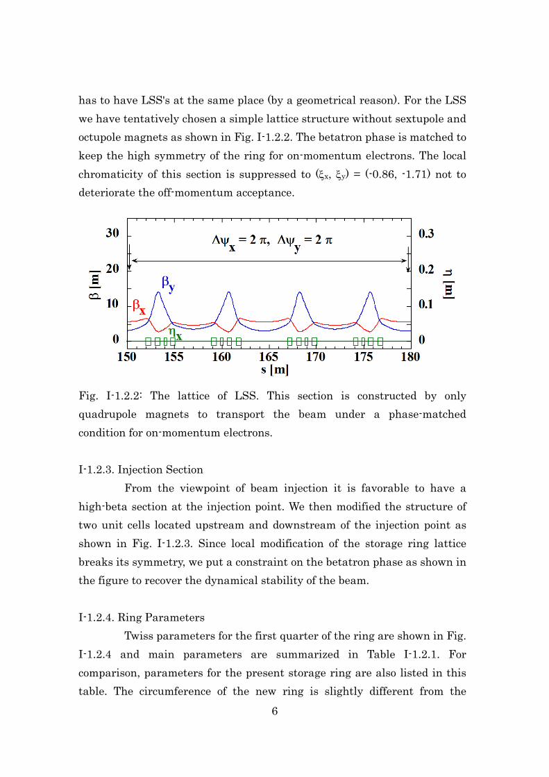
has to have LSS's at the same place (by a geometrical reason). For the LSS we have tentatively chosen a simple lattice structure without sextupole and octupole magnets as shown in Fig. I-1.2.2. The betatron phase is matched to keep the high symmetry of the ring for on-momentum electrons. The local chromaticity of this section is suppressed to (ξx, ξy) = (-0.86, -1.71) not to deteriorate the off-momentum acceptance.
Fig. I-1.2.2: The lattice of LSS. This section is constructed by only quadrupole magnets to transport the beam under a phase-matched condition for on-momentum electrons. I-1.2.3. Injection Section
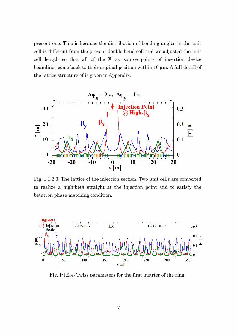
From the viewpoint of beam injection it is favorable to have a high-beta section at the injection point. We then modified the structure of two unit cells located upstream and downstream of the injection point as shown in Fig. I-1.2.3. Since local modification of the storage ring lattice breaks its symmetry, we put a constraint on the betatron phase as shown in the figure to recover the dynamical stability of the beam. I-1.2.4. Ring Parameters
Twiss parameters for the first quarter of the ring are shown in Fig. I-1.2.4 and main parameters are summarized in Table I-1.2.1. For comparison, parameters for the present storage ring are also listed in this table. The circumference of the new ring is slightly different from the
7
present one. This is because the distribution of bending angles in the unit cell is different from the present double-bend cell and we adjusted the unit cell length so that all of the X-ray source points of insertion device beamlines come back to their original position within 10 µm. A full detail of the lattice structure of is given in Appendix.
Fig. I-1.2.3: The lattice of the injection section. Two unit cells are converted to realize a high-beta straight at the injection point and to satisfy the betatron phase matching condition.
Fig. I-1.2.4: Twiss parameters for the first quarter of the ring.
8
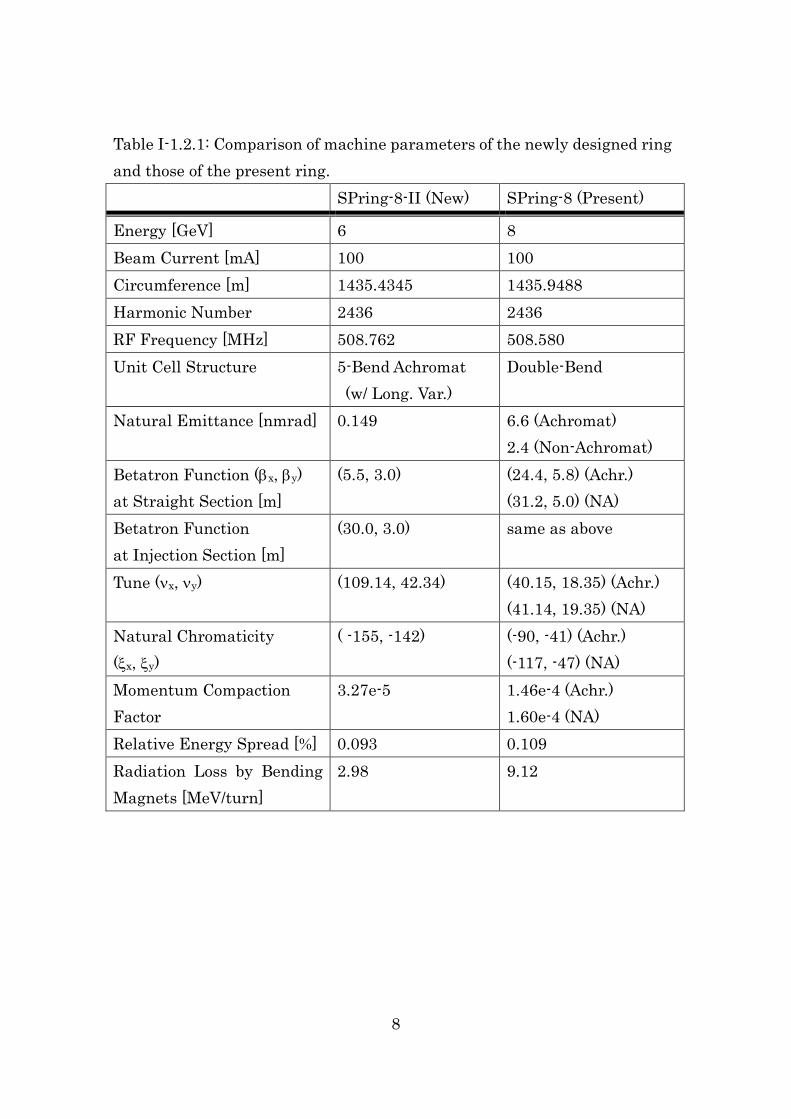
Table I-1.2.1: Comparison of machine parameters of the newly designed ring and those of the present ring. SPring-8-II (New) SPring-8 (Present)
Energy [GeV] 6 8 Beam Current [mA] 100 100 Circumference [m] 1435.4345 1435.9488 Harmonic Number 2436 2436 RF Frequency [MHz] 508.762 508.580 Unit Cell Structure 5-Bend Achromat
(w/ Long. Var.) Double-Bend
Natural Emittance [nmrad] 0.149 6.6 (Achromat) 2.4 (Non-Achromat)
Betatron Function (βx, βy) at Straight Section [m]
(5.5, 3.0) (24.4, 5.8) (Achr.) (31.2, 5.0) (NA)
Betatron Function at Injection Section [m]
(30.0, 3.0) same as above
Tune (νx, νy) (109.14, 42.34) (40.15, 18.35) (Achr.) (41.14, 19.35) (NA)
Natural Chromaticity (ξx, ξy)
( -155, -142) (-90, -41) (Achr.) (-117, -47) (NA)
Momentum Compaction Factor
3.27e-5 1.46e-4 (Achr.) 1.60e-4 (NA)
Relative Energy Spread [%] 0.093 0.109 Radiation Loss by Bending Magnets [MeV/turn]
2.98 9.12

9
I-1.3. Beam Dynamics Issues I-1.3.1. Dynamic Aperture and Momentum Acceptance
It is important to enlarge the dynamic aperture and momentum acceptance so as to achieve smooth commissioning and stable operation of the upgraded ring. In our design, sextupole magnets are located only in the arc sections and the betatron phase between the two arc sections in the unit cell are set to be (2n+1)π. Then, dominant effects of non-linear kicks due to sextupoles can be suppressed under this phase-matched condition. Though this interleaved-sextupole scheme [Brown1979, Emery1989, Oide1993, Soutome2008] works to a certain extent, the cancellation is not enough for achieving the required stability. We therefore introduced octupole magnets as a knob for the control of amplitude-dependent tuneshifts to increase the degree of freedom for suppressing the nonlinearity, i.e., the first- and second-order chromaticities, the amplitude-dependent tune shifts and the excitation strength of nonlinear resonances due to sextupoles and octupoles. The tuning knobs we used presently are (a) sextuople and octupole strengths, (b) betatron phase differences between the arcs, (c) betatron tunes per unit cell and (d) a ring operation point.
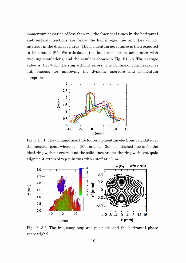
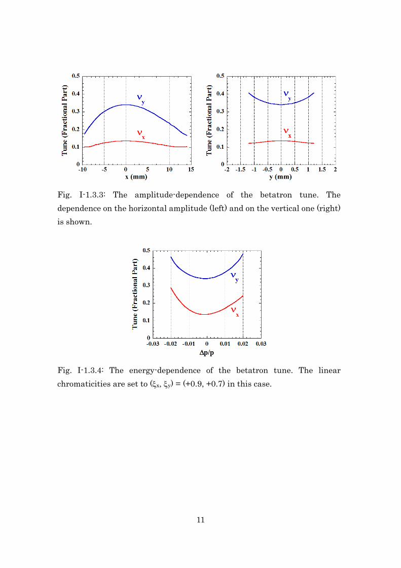
Figure I-1.3.1 shows a typical example of the dynamic aperture after the nonlinear optimization calculated with a symplectic tracking code CETRA [Schimizu2006]. We also show the result of frequency-map analysis and the horizontal phase space in Fig. I-1.3.2. The amplitude-dependent tune shifts are plotted in Fig. I-1.3.3. As discussed later in detail, a high-quality beam from SACLA can reduce a coherent injection amplitude down to ~3mm. The dynamic aperture shown here is thus large enough for the beam injection presently planned. We note that in Fig. I-1.3.2 there is an island above the main aperture area around the origin. We evaluate that such an island structure scarcely affects the injection efficiency because the injected beam emittance is small and electrons are well within the main aperture area.
As for the off-momentum stability we plot the energy-dependence of the betatron tune (nonlinear chromaticity) in Fig. I-1.3.4. For the
10
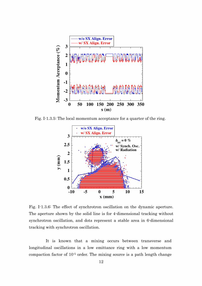
momentum deviation of less than 2%, the fractional tunes in the horizontal and vertical directions are below the half-integer line and they do not intersect in the displayed area. The momentum acceptance is then expected to be around 2%. We calculated the local momentum acceptance with tracking simulations, and the result is shown in Fig. I-1.3.5. The average value is 1.96% for the ring without errors. The nonlinear optimization is still ongoing for improving the dynamic aperture and momentum acceptance.
Fig. I-1.3.1: The dynamic aperture for on-momentum electrons calculated at the injection point where βx = 30m and βy = 3m. The dashed line is for the ideal ring without errors, and the solid lines are for the ring with sextupole alignment errors of 25µm in rms with cutoff at 50µm.
Fig. I-1.3.2: The frequency map analysis (left) and the horizontal phase space (right).
11
Fig. I-1.3.3: The amplitude-dependence of the betatron tune. The dependence on the horizontal amplitude (left) and on the vertical one (right) is shown.
Fig. I-1.3.4: The energy-dependence of the betatron tune. The linear chromaticities are set to (ξx, ξy) = (+0.9, +0.7) in this case.
12
Fig. I-1.3.5: The local momentum acceptance for a quarter of the ring.
Fig. I-1.3.6: The effect of synchrotron oscillation on the dynamic aperture. The aperture shown by the solid line is for 4-dimensional tracking without synchrotron oscillation, and dots represent a stable area in 6-dimensional tracking with synchrotron oscillation.
It is known that a mixing occurs between transverse and
longitudinal oscillations in a low emittance ring with a low momentum compaction factor of 10-5 order. The mixing source is a path length change
13
caused by a transverse deviation in a strong quadrupole and sextupole magnets. We checked this effect by tracking simulations with RF voltage switched on. As shown in Fig. I-1.3.6 the significant reduction of the dynamic aperture is not observed so far. Further investigation to suppress the mixing effect has been continued. I-1.3.2. Beam Lifetime
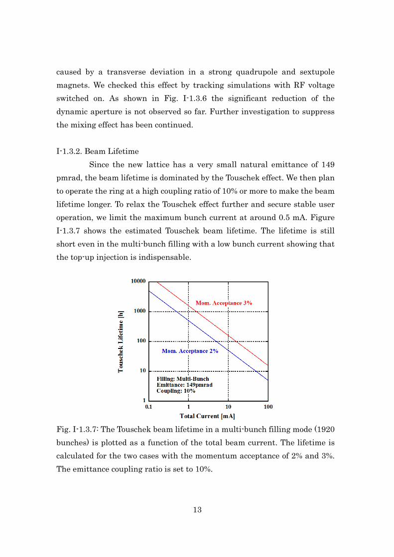
Since the new lattice has a very small natural emittance of 149 pmrad, the beam lifetime is dominated by the Touschek effect. We then plan to operate the ring at a high coupling ratio of 10% or more to make the beam lifetime longer. To relax the Touschek effect further and secure stable user operation, we limit the maximum bunch current at around 0.5 mA. Figure I-1.3.7 shows the estimated Touschek beam lifetime. The lifetime is still short even in the multi-bunch filling with a low bunch current showing that the top-up injection is indispensable.
Fig. I-1.3.7: The Touschek beam lifetime in a multi-bunch filling mode (1920 bunches) is plotted as a function of the total beam current. The lifetime is calculated for the two cases with the momentum acceptance of 2% and 3%. The emittance coupling ratio is set to 10%.

14
The intra-beam scattering (IBS) effect is generally not so large under the condition with the high coupling ratio and low bunch current. We checked the IBS effect on the beam emittance and energy spread by using Bane's formula [Bane2002]. The calculation results show that an increment of the emittance is only 3.2% and that of the energy spread is 0.5% when the natural emittance is ε0 = 149 pmrad. The emittance can potentially decrease to ~100 pmrad when most of undulator gaps are closed. Even in such a lower emittance case, evaluated increments of the emittance and the energy spread are 6.1% and 0.7%, respectively. I-1.3.3. Effects of Insertion Devices
Since we plan to lower the beam energy from 8 to 6 GeV, which leads to a shorter undulator period for generating hard X-rays, the effect of insertion devices (ID's) on the electron beam becomes larger than the present ring. We then estimated the effect of ID's on the tune shift, beta-distortion and the dynamic aperture. The calculations were performed in a symplectic manner [Forest1992] with 34 planar ID's having the following parameters: period length λ = 18mm, number of period N = 200, total length L = 3.6m and K value of 2.3. The dynamic aperture shrank to almost zero in the vertical direction due to a large vertical tune shift of +0.077 and vertical beta-distortion of 8.4% (rms) . We then tried to recover the dynamic aperture and found that a combination of local beta- and global tune- corrections is effective for restoration of the dynamic aperture. The present investigation suggests that a sophisticated scheme to correct the distortions by ID’s is necessary for a stable operation of the new ring and the study on developing such a scheme is under progress.
Another effect of ID's is the radiation damping. Figure I-1.3.8 shows the emittance and the relative energy spread as a function of the undulator K-value. In this calculation we assumed that the above 34 ID's are fully in use at the same K value. The emittance goes down to 100 pmrad when gaps of all the ID’s are closed at a K-value of 1.34.

15
Fig. I-1.3.8: A change of the emittance ε and the relative energy spread δ as a function of the undulator K value. It is assumed that 34 planar undulators (λ = 18mm, N = 200) are in use at the same K-value. For example, a K value of 1.34 corresponds to the photon energy of 10keV.
I-1.3.4. Alignment and Field Errors
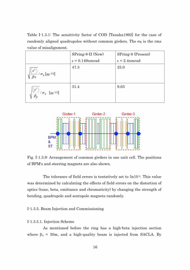
Since the quadrupole strengths required for the new ring are stronger than the present, we investigated the sensitivity factor of COD for the misalignment of quadrupole magnets. For the case of randomly aligned quadrupoles without common girders, we obtain the results shown in Table I-1.3.1. We see that the sensitivity of the new ring is 1.9 times higher in the horizontal direction and 3.3 times higher in the vertical direction when compared to the present ring. For smooth commissioning of the new ring, it is important to reduce the sensitivity factor as much as one can. We then plan to introduce common girders [Tanaka1992] as shown in Fig. I-1.3.9. By using such common girders the sensitivity factor can be reduced by a factor of 1.9 in the horizontal direction and 2.5 in the vertical direction. Based on these calculations we set the tentative alignment tolerance as follows: • Girder: better than 75 µm in rms with cutoff at 150 µm • Magnet on Girder: better than 25 µm in rms with cutoff at 50 µm
16
Table I-1.3.1: The sensitivity factor of COD [Tanaka1992] for the case of randomly aligned quadrupoles without common girders. The σR is the rms value of misalignment. SPring-8-II (New)
ε = 0.149nmrad SPring-8 (Present) ε = 2.4nmrad
[m-1/2] 47.3 25.0
[m-1/2] 31.4 9.63
Fig. I-1.3.9: Arrangement of common girders in one unit cell. The positions of BPM's and steering magnets are also shown.
The tolerance of field errors is tentatively set to 5x10⁻⁴. This value was determined by calculating the effects of field errors on the distortion of optics (tune, beta, emittance and chromaticity) by changing the strength of bending, quadrupole and sextupole magnets randomly. I-1.3.5. Beam Injection and Commissioning I-1.3.5.1. Injection Scheme
As mentioned before the ring has a high-beta injection section where βx = 30m, and a high-quality beam is injected from SACLA. By
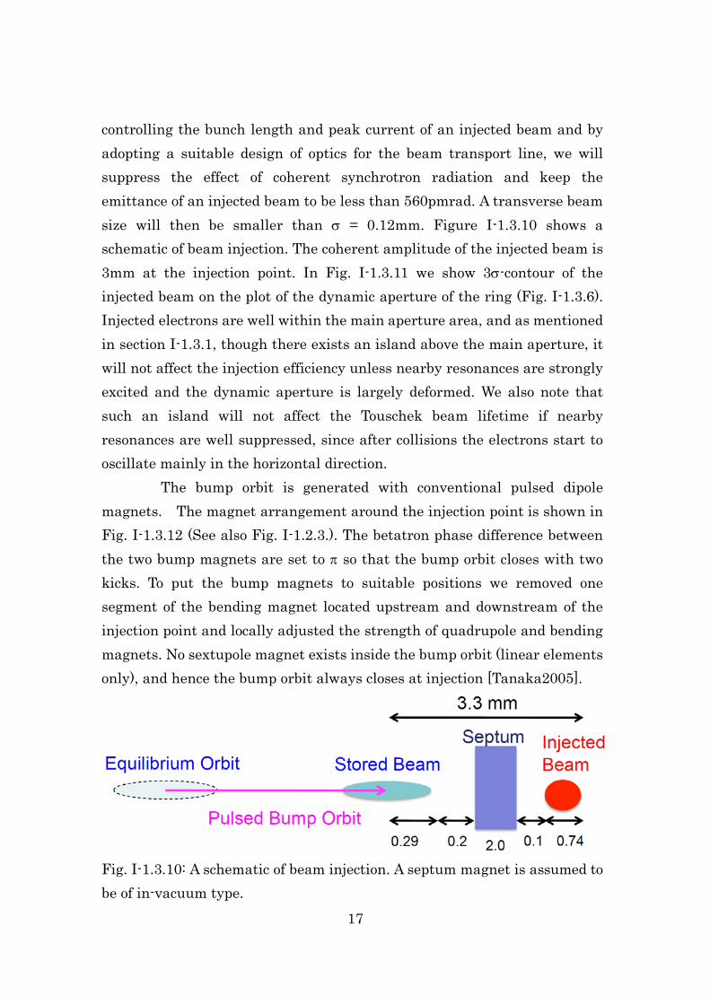
17
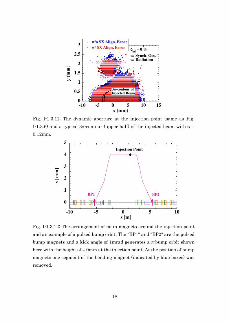
controlling the bunch length and peak current of an injected beam and by adopting a suitable design of optics for the beam transport line, we will suppress the effect of coherent synchrotron radiation and keep the emittance of an injected beam to be less than 560pmrad. A transverse beam size will then be smaller than σ = 0.12mm. Figure I-1.3.10 shows a schematic of beam injection. The coherent amplitude of the injected beam is 3mm at the injection point. In Fig. I-1.3.11 we show 3σ-contour of the injected beam on the plot of the dynamic aperture of the ring (Fig. I-1.3.6). Injected electrons are well within the main aperture area, and as mentioned in section I-1.3.1, though there exists an island above the main aperture, it will not affect the injection efficiency unless nearby resonances are strongly excited and the dynamic aperture is largely deformed. We also note that such an island will not affect the Touschek beam lifetime if nearby resonances are well suppressed, since after collisions the electrons start to oscillate mainly in the horizontal direction.
The bump orbit is generated with conventional pulsed dipole magnets. The magnet arrangement around the injection point is shown in Fig. I-1.3.12 (See also Fig. I-1.2.3.). The betatron phase difference between the two bump magnets are set to π so that the bump orbit closes with two kicks. To put the bump magnets to suitable positions we removed one segment of the bending magnet located upstream and downstream of the injection point and locally adjusted the strength of quadrupole and bending magnets. No sextupole magnet exists inside the bump orbit (linear elements only), and hence the bump orbit always closes at injection [Tanaka2005].
Fig. I-1.3.10: A schematic of beam injection. A septum magnet is assumed to be of in-vacuum type.
18
Fig. I-1.3.11: The dynamic aperture at the injection point (same as Fig. I-1.3.6) and a typical 3σ-contour (upper half) of the injected beam with σ = 0.12mm.
Fig. I-1.3.12: The arrangement of main magnets around the injection point and an example of a pulsed bump orbit. The "BP1" and "BP2" are the pulsed bump magnets and a kick angle of 1mrad generates a π-bump orbit shown here with the height of 4.0mm at the injection point. At the position of bump magnets one segment of the bending magnet (indicated by blue boxes) was removed.

19
I-1.3.5.2. Commissioning Scenario From simulations we found that the injected beam cannot be
stored without orbit correction when magnets and girders are aligned with rms errors of 25µm and 75µm, respectively. This is due to the fact that the dynamic aperture is small and the sensitivity factor is about a few times larger (Section I-1.3.4.) than the present ring. We hence start the beam commissioning with on-axis injection. Our scenario of beam commissioning is described below. (i) First-Turn Steering with On-Axis Injection: We measure a beam trajectory with single-pass BPM's and determine the kick angle of the first steering magnet so that the readout of a downstream BPM becomes zero (within a tolerance). We repeat the same procedure for the next steering magnet and fix the strength of all steering magnets on by one. Then, after one turn we can obtain an initial set of steering strengths for the COD correction. (ii) Beam Storage: By computer simulations we tested the above scheme when magnets and girders are aligned with rms errors of 25µm and 75µm, respectively. The results were promising: by using a set of steering strengths obtained with the above procedure, we calculated the dynamic aperture and found that it is large enough for proceeding to the tuning of off-axis injection for accumulation. (iii) Fine Correction of COD: After the beam storage with off-axis injection, we can experimentally measure COD, and based on it, we make fine orbit corrections. At this stage the dynamic aperture will be recovered further.
After we succeed in accumulation, we do machine tuning such as beta-distortion correction at a relatively low current (less than 20mA) since the Touschek beam lifetime is expected to be short (see Fig. I-1.3.7) at this very early stage of the machine tuning. For improving the beam lifetime, injection efficiency, emittance and other parameters, we continue the machine tuning step by step.
20
References of I-1.2 & I-1.3 [Bane2002] K. L. F. Bane, in Proc. of EPAC2002, p.1443; K. L. F. Bane, et al., Phys. Rev. ST Accel. Beams 5 (2002) 084403. [Brown1979] K. L. Brown, IEEE Trans. Nucl. Sci. NS-26 (1979) 3490. [Emery1989] L. Emery, in Proc. of 1989 IEEE PAC, p.1225. [Farvacque2013] L. Farvacque, et al., in Proc. of IPAC2014, p.79. [Forest1992] E. Forest and K. Ohmi, KEK Report 92-14 (1992). [Nagaoka2007] R. Nagaoka and A. F. Wrulich, Nucl. Instr. and Meth. in Phys. Res. A575 (2007) 292. [Oide1993] K. Oide and H. Koiso, Phys. Rev. E47 (1993) 2010. [Revol2013] J-L. Revol, et al., in Proc. of IPAC2014, p.1140. [Schimizu2006] Tracking simulations were carried out by using an in-house symplectic code CETRA; J.Schimizu, et al., in Proc. of 13th Symposium on Acc. Science and Technology, Osaka (2001), p.80; J.Schimzu, "Workshop SAD2006", Tsukuba. http://acc-physics.kek.jp/SAD/SAD2006/ [Soutome2008] K. Soutome, et al., in Proc. of EPAC2008, p.3149. [Tanaka1992] H. Tanaka, et al., Nucl. Instr. and Meth. in Phys. Res. A313 (1992) 529. [Tanaka2005] H. Tanaka, et al., Nucl. Instr. and Meth. in Phys. Res. A539 (2005) 547.
21
I-1.4. Magnet System I-1.4.1. Overview
Main requirements for the magnet system are listed in Table I-1.4.1. The five-bend lattice of SPring-8-II is composed of a normal bending magnet at the center of the cell and four other bending magnets with longitudinal field gradient. Here, we shall call such a bend with the field gradient a longitudinal gradient bend, or L.G.B. The new lattice needs not only 2.5 times more bending magnets than the current SPring-8 storage ring does, but also more quadrupole and sextupole magnets in between. In total, 944 quadrupoles, including 64 for long straight sections, and 352 sextupoles are necessary in addition to other magnets such as octupoles and steerings. On the other hand, it is a common issue in designing extremely small emittance rings that integrated field strengths of the multi-pole magnets become higher. It is the case for us, too. Although a longer magnet help mitigate a magnetic field of each component, it is necessary to consider a trade-off between the peak magnetic field and the packing factor. Thus, the lattice has been designed with the magnet settings as shown in Table I-1.4.1 so that we can make sure that the field gradients are available by existing technologies.
Table I-1.4.1: Main requirements for magnets.
Dipole
Quadrupole Sextupole Norm. B. L.G.B.
#/normal cell 1 4 20 8
Total # magnets 44 176 880+64 352
Max. field 0.953 T 0.775 T 55.4 T/m 2,620 T/m2
Gap/Bore dia. [mm] 25 25 34 36
GFR [mm] ±12 ±12 ±12 ±12
Field error
between magnets 5 x 10⁻⁴ 5 x 10⁻⁴ 5 x 10⁻⁴ 5 x 10⁻⁴
Norm. B.: normal bending magnet. L.G.B.: Longitudinal gradient bend.
GFR: Good field region where the integrated field deviation is within 10-3.
22
Good field regions for the integrated field deviation of within 10-3 are all assumed to be ±12 mm, and integrated field errors between magnets are assumed to be less than 5 x 10⁻⁴. Independent requirements for the magnets may be further discussed in detail.
I-1.4.2. Dipole Magnet
Dipole magnets are designed as shown in Fig. I-1.4.1(a)(b), and the major specifications are summarized in Table I-1.4.2. In order to reduce power consumption, we plan to apply permanent magnet to dipole magnets [Chavanne2014]. Both the normal and the longitudinal gradient bending magnets are C-shaped sector type with a gap of 25 mm. The C-type is chosen because we intend to install and de-install, if necessary, vacuum chambers without moving a gap of the permanent magnet. Instead the bending magnets will be horizontally moved in and out without interfering with vacuum chambers.
Due to a hybrid structure consisting of permanent magnet and irons, a magnetic field distribution on beam axis is smoothed out even if there is inhomogeneous magnetization of permanent magnet pieces. Further, since the permanent magnet pieces are placed far from the beam axis, a degradation of the magnetization by radiation is supposed to be significantly suppressed. Another notable feature is that "outer plates" will be embedded with the magnet so that the magnetic field on beam axis can be adjusted by changing the outer plate positions. This helps obtain the matching between the magnetic field and the nominal electron energy at the initial installation, and also change the operating energy for some specific purposes. The energy tuning range by the outer plates can be more than 10 % [Watanabe2014].
Fringe fields in the longitudinal axis need to be suppressed as low as possible for the magnets to fit in the designed lattice. The gap of the bending magnets, therefore, is fixed at 25 mm for both normal and longitudinal gradient bends. The field gradient of L.G.B. required by the lattice is produced by the gradients of permanent magnet distribution and
23
outer plate positions. The magnetic resistance along the longitudinal axis is enhanced by spacing between the magnets as shown in Fig. I-1.4.1.
Detailed designs of the permanent magnets are under development. As an example, since the temperature coefficient of remanent induction for Neodymium permanent magnet is -0.12 %/K, a temperature drift of ambient air will distort the lattice functions and dynamic apertures. Thus, the magnet temperature has to be stabilized within a fraction of degree, which we assume is feasible.
Table I-1.4.2: Major specifications of bending magnets. Normal bend L.G.B. (2 types)
Magnetic field [T] 0.953 0.166, 0.296, 0.582 / 0.221, 0.395, 0.775
Effective length [m] 0.42 0.7, 0.7, 0.35
Gap [mm] 25 25
Fig. I-1.4.1: Normal and longitudinal gradient bending magnets. (a) Cross section of normal bending magnet. (b) Longitudinal gradient bend (bird view).
24
I-1.4.3. Quadrupole, Sextupole, and Octupole Magnets Quadrupole magnets are designed as shown in Fig. I-1.4.2 and
Table I-1.4.3. All quadrupoles have the same cross sectional design, but are grouped by the longitudinal lengths into 7 groups (Leff = 0.20, 0.24, 0.30, 0.50, 0.55, 0.65, and 0.70 m). A bore diameter of 34 mm is defined by the maximum field gradient, 56 T/m, and the relatively small diameter is also preferred from the viewpoints of power consumption and fringe field along the longitudinal axis.
A coil distribution is one of key issues in the design. As a high packing factor is the most challenging in the design of extremely small emittance ring, magnets ought to be compact longitudinally, yet the peak field should not exceed the maximum value we set. Further, power consumption should be kept as low as possible. Considering these factors, a coil distribution is designed as indicated in Fig. I-1.4.2. In the design, coils stick out of the effective length of magnet by just 10.5 mm in each side.
Since the quadrupole magnet will be divided into four segments in an assembly and when vacuum chambers will be installed/de-installed. Repeatability of physical mounting of the segments has to be secured [Ohnishi1996]. For the purpose, the return yoke is made slightly thicker than it is needed in terms of magnetic saturation.
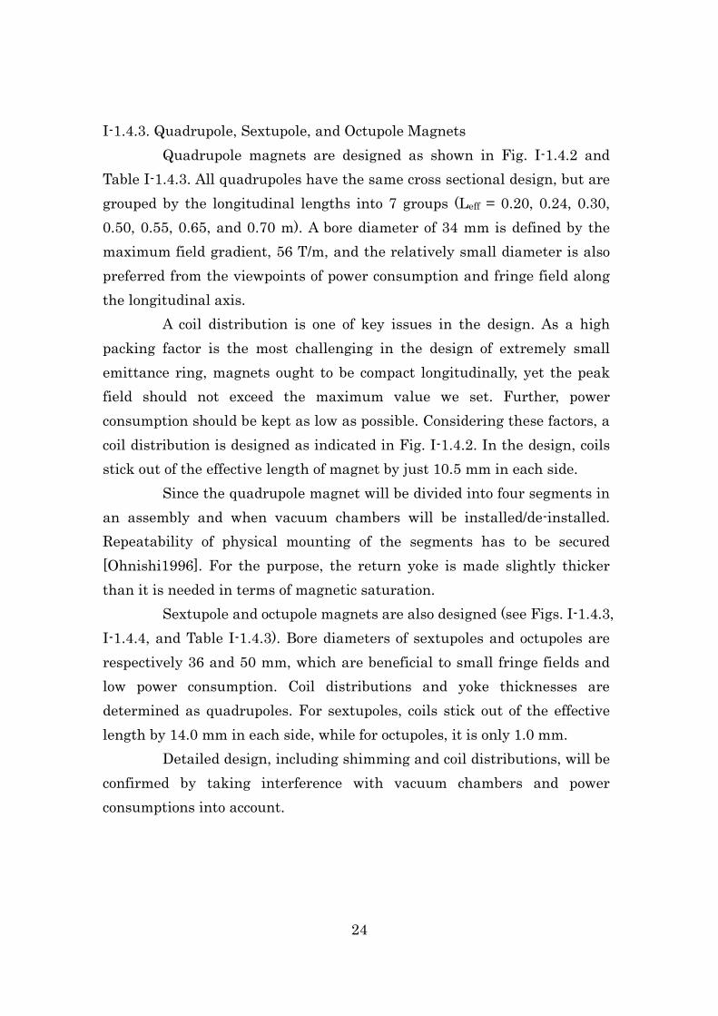
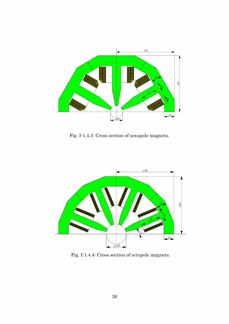
Sextupole and octupole magnets are also designed (see Figs. I-1.4.3, I-1.4.4, and Table I-1.4.3). Bore diameters of sextupoles and octupoles are respectively 36 and 50 mm, which are beneficial to small fringe fields and low power consumption. Coil distributions and yoke thicknesses are determined as quadrupoles. For sextupoles, coils stick out of the effective length by 14.0 mm in each side, while for octupoles, it is only 1.0 mm.
Detailed design, including shimming and coil distributions, will be confirmed by taking interference with vacuum chambers and power consumptions into account.

25
Table I-1.4.3: Major specifications of quadrupoles and sextupoles. Quadrupole Sextupole
Max. Field gradient [T/m, T/m2] 55.4 2,620 Effective length [mm] 200 - 700 180, 300
Pole length [mm] 181 - 681 168, 288 Total length incl. coil [mm] 221 - 721 208, 328
Bore diameter [mm] 34 36 Max. current [A] 335 250
# turns/pole 21 9
Fig. I-1.4.2: Cross section of quadrupole magnets. Transverse dimensions and coil distributions are to be optimized for matching with vacuum chambers (same for sexutpoles and octupoles).
26
Fig. I-1.4.3: Cross section of sexupole magnets.
Fig. I-1.4.4: Cross section of octupole magnets.

27
I-1.4.4. Steering Magnet Like other magnets, a steering magnet needs to be designed so that
it can fit in the lattice. In order to spare a space, the magnet has both horizontal and vertical kicks in a single segment as shown in Fig.I-1.4.5. Main parameters are listed in Table I-1.4.4. The kick angle is evaluated to be 0.12 and 0.06 mrad in each axis. Detailed specifications of steering coils will be further discussed from the viewpoints of commissioning scenario and spacing.
Table I-1.4.4: Main parameters for steering magnets.
Kick direction Horizontal Vertical Gap [mm] 56 90
Integrated field [T-m] 2.45 x 10⁻³ 1.32 x 10⁻³ Kick angle [mrad] 0.12 0.06
Effective length [mm] 83 105 Pole length [mm] 50 50
Total length incl. coil [mm] 95 95 I-1.4.5. Power Supply
The power supplies and auxiliary infrastructures will be prepared, considering (1) to make full use of existing resources, (2) to save energy and
Fig. I-1.4.5: Steering magnet.
28
space, and yet (3) to achieve high performances. We plan to reuse cables and cooling system with minimum changings, while all power supplies that have been used for the current SPring-8 storage ring since 1990's are to be replaced with new technologies for meeting required specifications. Aiming at the power factor of 99 % and the power efficiency of 94 %, new power supplies will be equipped with the switching technology. It will be beneficial not only to save energy, but also to reduce housing sizes as well as loads to cooling system.
It has been observed at SPring-8 that the output currents of power supplies drift in hours to months due to ambient air temperature shift. By introducing a feedback, we expect to suppress the drift and ripple within 10 ppm.
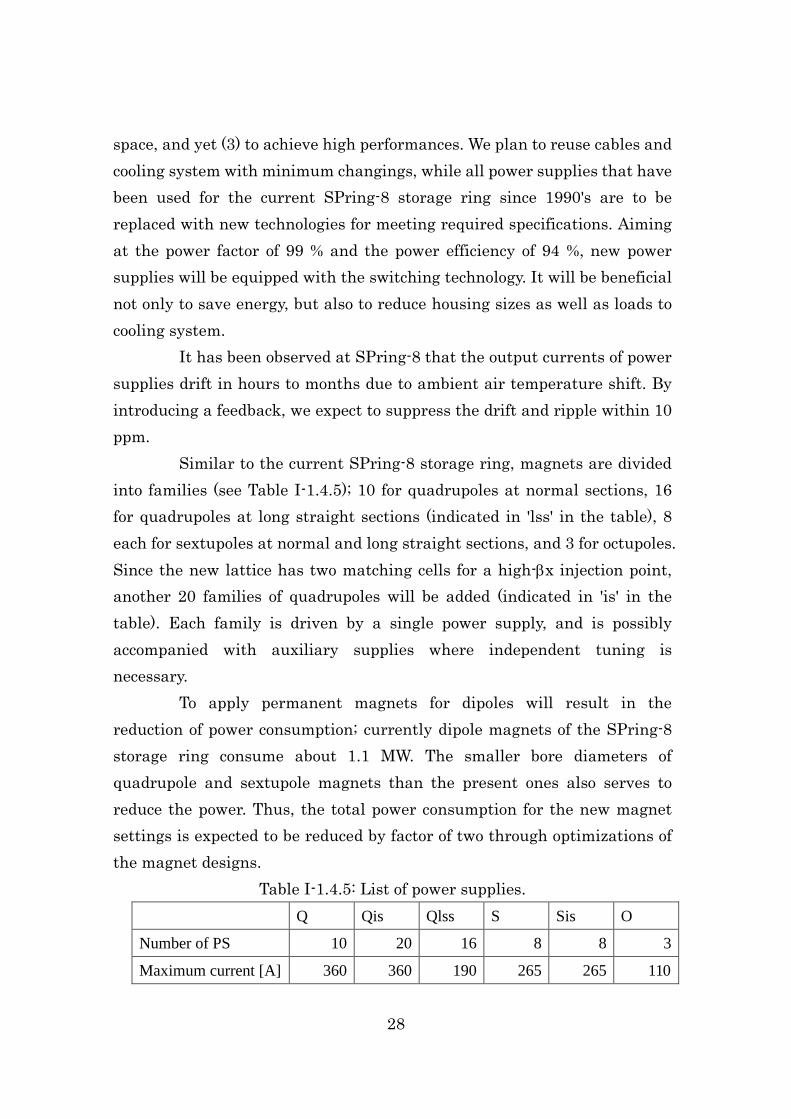
Similar to the current SPring-8 storage ring, magnets are divided into families (see Table I-1.4.5); 10 for quadrupoles at normal sections, 16 for quadrupoles at long straight sections (indicated in 'lss' in the table), 8 each for sextupoles at normal and long straight sections, and 3 for octupoles. Since the new lattice has two matching cells for a high-βx injection point, another 20 families of quadrupoles will be added (indicated in 'is' in the table). Each family is driven by a single power supply, and is possibly accompanied with auxiliary supplies where independent tuning is necessary.
To apply permanent magnets for dipoles will result in the reduction of power consumption; currently dipole magnets of the SPring-8 storage ring consume about 1.1 MW. The smaller bore diameters of quadrupole and sextupole magnets than the present ones also serves to reduce the power. Thus, the total power consumption for the new magnet settings is expected to be reduced by factor of two through optimizations of the magnet designs.
Table I-1.4.5: List of power supplies. Q Qis Qlss S Sis O
Number of PS 10 20 16 8 8 3
Maximum current [A] 360 360 190 265 265 110
29
I-1.4.6. Alignment In order to secure enough dynamic aperture, magnet alignment is
one of key issues in designing the new ring. The required goal of the alignment is 25 µm (rms) on a girder, and 75 µm (rms) between girders (see Section I-1.3.4.). Since better alignment helps obtain smaller COD and larger apertures, even better alignment, such as 10 µm (rms) on a girder, would be preferred. For the purpose, we plan to apply a combination of several alignment schemes based on laser schemes [Zhang2012] and a vibration wire method for the magnet alignment.
The vibrating wire method can be advantageous over other common schemes in a sense that there is no need to transfer a magnetic center to some fiducial point prior to the alignment [Jain2008, Temnykh1997, Fukami2014]; each magnet can be aligned while a wire directly senses the deviation of the magnetic center. We expect that magnets will be aligned within 20 µm (rms) or less by the wire method at the initial installation of magnets, then long-term drifts after the installation will be monitored by a laser that tracks fiducial points. The alignment between girders will be carried out by laser trackers as well [Zhang1995, Matsui1995, Tsumaki2002].
In a practical alignment procedure, not only to precisely measure a magnetic center but also to move a magnet with a good resolution and to obtain the good repeatability of magnet segments are essential. For that, mechanical structures such as a thickness of yokes, a stage for the fiducial point, and a magnetic support are carefully designed, taking these issues into account.

30
References [Chavanne2014] J. Chavanne and G.Le Bec, Proc. of IPAC'14, Dresden, Germany, TUZB01, p.968. [Fukami2014] K. Fukami et al., Proc. of IPAC'14, Dresden, Germany, MOPRO081, p.277. [Jain2008] A. Jain, et al., Proc. of the International Workshop on Accelerator Alignment 2008 (IWAA2008), Tsukuba, Japan, p.1. [Matsui1995] S. Matsui, et al., Proc. of the International Workshop on Accelerator Alignment 1995 (IWAA1995), Tsukuba, Japan (1995), p.174. [Ohnishi1996] J. Ohnishi, et al., IEEE Transactions on Magnetics 32 (1996) 3069. [Temnykh1997] A. Temnykh, et al., Nucl. Instrum. Meth. A 399 (1997) 185. [Tsumaki2002] K. Tsumaki et al., Proc. of the International Workshop on Accelerator Alignment 2002 (IWAA2002), Hyogo, Japan, p.210. [Watanabe2014] T. Watanabe, et al., Proc. of IPAC'14, Dresden, Germany, TUPRO092, p.1253. [Zhang1995] C. Zhang, et al., Proc. of the International Workshop on Accelerator Alignment 1995 (IWAA1995), Tsukuba, Japan (1995), p.185. [Zhang2012] C. Zhang, et al., Proc. of the International Workshop on Accelerator Alignment 2012 (IWAA2012), Batavia, U.S. (2012).

31
I-1.5. Vacuum System I-1.5.1. Design Concept
The design of a proper vacuum system, satisfying a lattice design for the targeted high-coherence ring of the upgrade project, holds the key to the success, which provides stable beam operation and highly brilliant synchrotron light. Several technical methods are applied to the new lattice design, which significantly affect the ring vacuum design. Not only arrangement of a large number of multi-pole magnets but also increase in number of photon absorbers, resulting from the multi-bend achromat configuration, brings severe space constraints. The constraints also have a substantial impact on designing vacuum components, such as bellows and gate valves. The extremely strong focusing of the magnets requires the miniaturization of vacuum chamber, which correlates the vacuum pumping design due to the low vacuum conductance. Furthermore, two other particular factors should be considered as well as the above requirements. One is the time constraints issue. All the replacement work, namely dismantlement, installation, alignment and evacuation to ultra-high-vacuum, should be done within a year followed by the beam commssioning and making the vacuum system fully outgassed as soon as possible. The other is that the new light extraction design for bending magnet beamlines should fit into the existing SPring-8 beamlines, although both light source point and light axis angle shall be naturally changed. Based on the above circumstances, some design concepts are presented. Baking strategy
It is apparently impossible to carry out the in-situ baking and the following non-evaporable getter (NEG) activation throughout a range of the ring after the installation because of the extremely severe time restrictions. On the other hand, even if the off-line baking is carried out in advance, to expose the vacuum surface to the air after the installation for vacuum connections and followed by conducting only the NEG activation without in-situ baking would be unreasonable. Hence, we plan to establish a highly performed and reasonable

32
procedure to realize the ultra-high vacuum (UHV) system in the tunnel within a limited amount of time, by completing the baking and NEG activation of a long integral chamber off-line before the black out with enough time to spare, and just by transporting and installing in the ring with UHV.
Pumping strategy Vacuum pumping will be mainly provided by discrete NEG cartridges integrated into a ConFlat Flange (CF), some of which combine a sputter ion pump (SIP) for the evacuation of CH4 and noble gases.
Vacuum chamber strategy The main chambers will be made from extruded aluminum alloy. Bending radiation is going to be intercepted by only discrete photon absorbers without directly irradiating any inner wall of vacuum chambers. As a result, an antechamber is necessary.
Light Extraction strategy The main prerequisite is to continue utilizing all the existing beamlines without making any alterations on shielding concrete structure of the existing SPring-8 storage ring tunnel.
Maintenance strategy Once a serious failure happens to a vacuum component, we plan to exchange entirely the troubled vacuum section delimited by transport gate valves (TGV; see section I-1.5.5.4). On the other hand, in case of a minor failure, ultra-high vacuum after the replacement work will be achieved under pure N2 purge, followed by non-baking or partial baking of SIP and NEG re-activation.
I-1.5.2. Vacuum Chamber I-1.5.2.1. Chamber Materials
Extruded aluminum alloy chamber (equivalent to A6063-T5), which has been used successfully at SPring-8, will be adopted because of the superior properties listed below:

33
・Easy forming of complex cross section by the extrusion; ・Low temperature rise caused by the wake field because of the high
electrical conductivity; ・High thermal conductivity resulting in relatively uniform temperature
distribution against heat generation from the baking and the wake field; ・Low radio-activation. I-1.5.2.2. Structural Design Straight section chambers The cross-section of the straight section chamber (SSC) is shown in Fig. I-1.5.1. The beam chamber (30 mm × 16 mm racetrack), which corresponds to the multi-pole magnets with a bore radius of 17 mm, is connected with an antechamber through a slot of 5 mm width for transporting the photon beam. The antechamber also works to enhance the vacuum conductance. The chamber has a cooling water channel to remove the heat generated by the wake field and the scattering light. The FEM analysis shows the maximum equivalent stress caused by the atmospheric pressure is well below the yield stress of 125 MPa at 150°C (Fig. I-1.5.2).
Fig. I-1.5.1: Extruded cross-section of the straight section chamber.
Fig. I-1.5.2: FEM structural analysis result of the straight section chamber.

34
Bending section chamber The bending section chamber (BSC), whose cross-section is shown
in Fig. I-1.5.3, will be manufactured by bending after the extrusion. The antechamber will be equipped with vacuum ports for inserting a photon absorber and the NEG pump.
Fig. I-1.5.3: Extruded cross-section of the bending section chamber.
Impedance of vacuum chambers
RF shielding such as a RF-finger or a RF-contact should be set inside bellows, gate valves and gaps between flanges to smooth the cross-section change for low impedance. When the RF-finger and the RF-contact are made of beryllium copper or stainless steal, they should be coated with silver or something high electrical conductance to decrease impedance. The change in the shape of the beam aperture should be designed to be a gentle tapered transition structure. I-1.5.2.3. Manufacturing and Treatment
The extruded chambers will be machined to prepare grooves of weld joint at both ends and some ports for the vacuum pumps and gauges. The detailed cleaning procedure for the UHV will be decided based on the results of R&D. To realize our baking strategy mentioned in section I-1.5.1, a vacuum unit cell would be divided into two sections, as shown in Fig. I-1.5.4, each of which has a half-cell length of about 12 m and mainly consists of SSCs and BSCs. To handle the severe space constraints issue, each section shall be a welded integral structure.

35
I-1.5.2.4. Evacuation and Baking with NEG Activation After all vacuum components and two TGVs are attached, the 12
m-long integral chamber (LIC) will be evacuated to UHV individually by off-line baking and the following NEG activation in advance.
Fig. I-1.5.4: Distribution map of photon absorbers and gate valves for a unit cell.
36
I-1.5.2.5. Installation and Alignment After the baking, rough alignment of the LIC will be conducted
off-line. Then, we are going to transport it to the ring tunnel under UHV and align it precisely inside the quadrupole and sextupole magnets whose upper half is removed. After the positional relation with the magnets is confirmed, C-type bending magnets will be installed from a lateral direction. As there are two LICs per unit cell, we are going to install a short joining chamber including the BM3 chamber to connect the LICs through the TGVs. We also install another joining chamber, which connects the LIC to the ID chamber. After the connections are finished in the tunnel, the joining chambers will be baked locally when necessary. Then, by opening the TGVs, the total vacuum system for a unit cell will be ready without exposing the vacuum surface to the air. In this way, the LICs will not be baked in the tunnel. I-1.5.3. Photon Absorbers I-1.5.3.1. Distribution
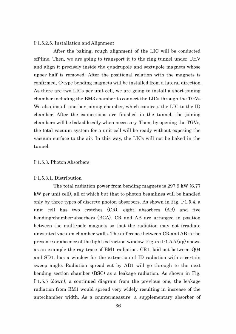
The total radiation power from bending magnets is 297.9 kW (6.77 kW per unit cell), all of which but that to photon beamlines will be handled only by three types of discrete photon absorbers. As shown in Fig. I-1.5.4, a unit cell has two crotches (CR), eight absorbers (AB) and five bending-chamber-absorbers (BCA). CR and AB are arranged in position between the multi-pole magnets so that the radiation may not irradiate unwanted vacuum chamber walls. The difference between CR and AB is the presence or absence of the light extraction window. Figure I-1.5.5 (up) shows as an example the ray trace of BM1 radiation. CR1, laid out between Q04 and SD1, has a window for the extraction of ID radiation with a certain sweep angle. Radiation spread cut by AB1 will go through to the next bending section chamber (BSC) as a leakage radiation. As shown in Fig. I-1.5.5 (down), a continued diagram from the previous one, the leakage radiation from BM1 would spread very widely resulting in increase of the antechamber width. As a countermeasure, a supplementary absorber of
37
BCA will be inserted into the downstream end of each BSC, which contributes to the miniaturization of the antechamber in a straight section chamber (SSC). Following this approach, the distance between the electron orbit and the end of antechamber can be kept to be 60 mm, as shown in Fig. I-1.5.1. The characters from A to C and from D to F shown in Fig. I-1.5.5 indicate longitudinally varying magnetic field regions in BM1 and BM2, respectively, as specified in Table I-1.4.2.
Fig. I-1.5.5: Ray trace of the BM1 (up) and the BM2 (down) radiations.
I-1.5.3.2. Material
The photon absorbers are going to be manufactured using Glidcop or oxygen free copper (OFC) as the situation demands based on a FEM analysis result. Basically, OFC will be used insofar as the maximum temperature is less than 200°C and in addition the maximum equivalent stress does not exceed yield point. For every case in excess of these criteria, Glidcop will be selected. As to the thermal limitation of a heat-absorbing
38
body made of Glidcop, we plan to use an evaluation method based on a low-cycle fatigue life prediction by using elasto-plastic analysis [Takahashi2008]. And the allowable number of cycles to failure will be set to be more than 10,000 cycles taking into consideration the top-up operation. I-1.5.3.3. Heat Load
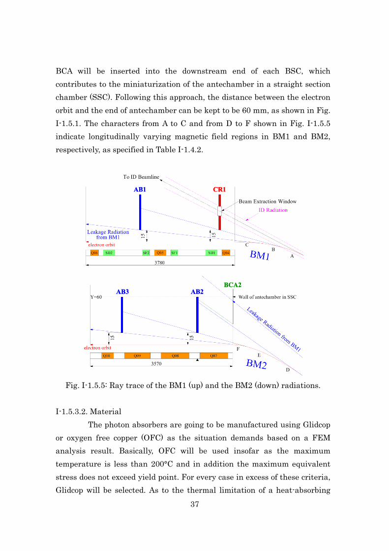
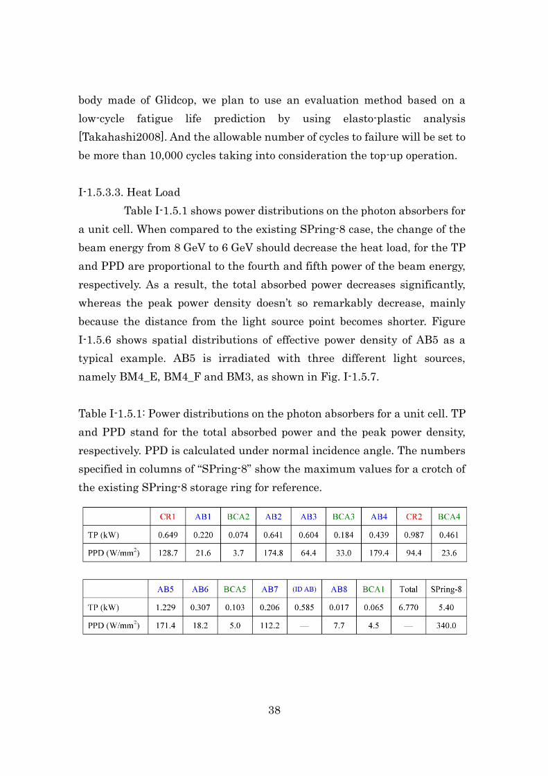
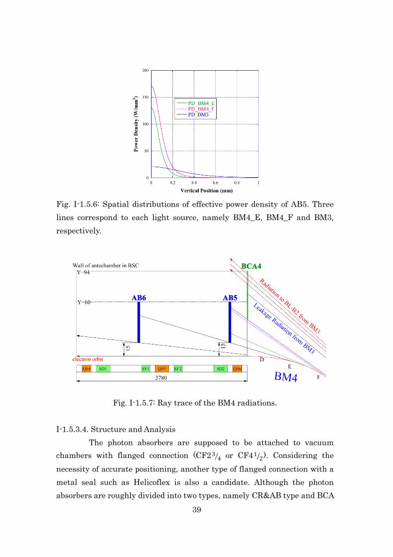
Table I-1.5.1 shows power distributions on the photon absorbers for a unit cell. When compared to the existing SPring-8 case, the change of the beam energy from 8 GeV to 6 GeV should decrease the heat load, for the TP and PPD are proportional to the fourth and fifth power of the beam energy, respectively. As a result, the total absorbed power decreases significantly, whereas the peak power density doesn’t so remarkably decrease, mainly because the distance from the light source point becomes shorter. Figure I-1.5.6 shows spatial distributions of effective power density of AB5 as a typical example. AB5 is irradiated with three different light sources, namely BM4_E, BM4_F and BM3, as shown in Fig. I-1.5.7.
Table I-1.5.1: Power distributions on the photon absorbers for a unit cell. TP and PPD stand for the total absorbed power and the peak power density, respectively. PPD is calculated under normal incidence angle. The numbers specified in columns of “SPring-8” show the maximum values for a crotch of the existing SPring-8 storage ring for reference.
39
Fig. I-1.5.6: Spatial distributions of effective power density of AB5. Three lines correspond to each light source, namely BM4_E, BM4_F and BM3, respectively.
Fig. I-1.5.7: Ray trace of the BM4 radiations. I-1.5.3.4. Structure and Analysis
The photon absorbers are supposed to be attached to vacuum chambers with flanged connection (CF23
4� or CF412� ). Considering the
necessity of accurate positioning, another type of flanged connection with a metal seal such as Helicoflex is also a candidate. Although the photon absorbers are roughly divided into two types, namely CR&AB type and BCA

40
type, downsizing design with proper cooling ability is a common target. Most of CR&AB can be installed horizontally into its exclusive chamber, which has the same cross section as SSC, whereas AB1 and AB5 should be vertically so as to prevent the interference with the light extraction line. On the other hand, BCA must be installed into BSC so that it is necessary to make the thickness of heat-absorbing body thin enough. In addition, BCA4 needs to have a beam extraction window, which would introduce BM3 radiation with a certain sweep angle to the existing SPring-8 BM2 beamline (B2-BL). Basically simple grazing angle configuration for reducing effective power density will be applied to the irradiated area for either type. As for the cooling water design, we have to keep it in mind that a cooling channel should not be arranged at the just downstream side of the irradiated area in the same plane as the electron orbit in order to avoid corrosion of copper resulting from the interaction between cooling water and synchrotron radiation. To keep the velocity of cooling water as low as possible within the thermally allowable range is also important as a countermeasure to severe vibration issue. Figure I-1.5.8 shows a schematic drawing of BCA4 as an example. Depending on the results of thermal and thermo-mechanical analyses by using FEM, which are ongoing, the irradiated area and the cooling channel configurations are to be optimized.
Fig. I-1.5.8: External (left) and cross-sectional (right) views of schematic drawings of
BCA4.

41
I-1.5.4. Pressure in the Vacuum System I-1.5.4.1. Beam Lifetime
In case of an ultra low emittance ring, not the gas scattering lifetime (τg) decided by vacuum pressure but the Touschek lifetime (τT) by intrabeam scattering naturally dominates the beam lifetime (τtotal). The correlation among them is given by equation (I-1.5.1),
1𝜏𝑡𝑜𝑡𝑎𝑙
= 1𝜏𝑔
+ 1𝜏𝑇
(I-1.5.1)
As for the new ring, the τT is estimated to be about as small as 12 h. As the τtotal is aimed to be kept at 10 h of a 20 % reduction from the 12 h, we set a targeted τg to 60 h. As is well known, the τg depends on three collision scattering processes, namely Rutherford scattering (τR), Bremsstrahlung (τB) and Möller scattering (τM). τg are written as
1𝜏𝑔
= 1𝜏𝑅
+ 1𝜏𝐵
+ 1𝜏𝑀
= 𝑐𝑁∑ �𝜎𝑅𝑖 + 𝜎𝐵𝑖 + 𝑍𝑖𝜎𝑀�𝑖 (I-1.5.2)
where c is a speed of light, N is a number of molecules, σj (j = Ri, Bi, Mi) is a cross-section of each scattering process, and 𝑍𝑖 is atomic number of molecules species i. In the case of narrow vacuum chamber of inner aperture, Rutherford scattering becomes dominant. Cross-section of Rutherford scattering is
𝜎𝑅𝑖 = 4𝜋𝑍𝑖2𝑟𝑒2
𝛾2𝜃𝑐2 (I-1.5.3)
where re = 2.818×10⁻¹⁵ and γ is a Lorentz factor. In case of elliptical cross section as inner shape of vacuum chamber, 1/θc2 is
1𝜃𝑐2
= ⟨𝛽𝑥⟩𝛽𝑥𝑚
2𝑎𝑥2+ ⟨𝛽𝑥⟩𝛽𝑥𝑚
2𝑎𝑦2 (I-1.5.4)
where <βx,y>, 𝑎𝑥,𝑦 , βmx,y (x; horizontal, y; vertical) are an average of betatron function, the half-size of the minimum aperture and the betatron function at that aperture, respectively.
Table I-1.5.2 shows parameters for the calculation of τg based on the cross section of the vacuum chamber shown in Fig. I-1.5.1. It should be

42
noted that 𝑎𝑦 and βm y naturally vary depending on the in-vacuum ID gap.
Figure I-1.5.9 shows the expected relationship between the gas scattering lifetime 𝜏𝑔𝑖 and the partial pressure 𝑃𝑖 of typical residual gases when ID gap is fully opened. The products of 𝜏𝑔𝑖 (h) and partial pressure 𝑃𝑖 (Pa) for typical residual gases are constant values. These values are shown in Table I-1.5.3 for the calculation of beam lifetime in the section of I-1.5.4.2.3.
Table I-1.5.2: Parameters of the new ring for the calculation of gas scattering lifetime when the conditions of ID gap are fully opened and 5 mm, respectively.
Parameter ID gap: fully opened ID gap: 5 mm
Min. vertical aperture (half-size); 𝑎𝑦 [m] 0.008 0.0025
Min. horizontal aperture (half-size); 𝑎𝑥 [m] 0.015 0.015
βm y [m] at 𝑎𝑦 27 4.08
βm x [m] at 𝑎𝑥 30 30
Average <βy> [m] 14 14
Average <βx> [m] 7 7
γc/γ 0.02 0.02
Fig. I-1.5.9: Relationship between the gas scattering lifetime and the partial pressure of typical residual gases by the parameters (Table I-1.5.2) of the new ring in the case of fully opened ID gap.

43
Table I-1.5.3: The products of gas scattering lifetime 𝜏𝑔𝑖 (h) and partial pressure (𝑃𝑖(Pa)) for typical residual gases at 6 GeV. 𝜏𝑔𝑖 × 𝑃𝑖 (Pa·h) H2 CH4 H2O CO CO2 ID gap: fully opened 1.29 × 10⁻⁴ 1.08 × 10⁻⁵ 7.15 × 10⁻⁶ 4.78 × 10⁻⁶ 2.95 × 10⁻⁶
ID gap: 5mm 1.14 × 10⁻⁴ 9.37 × 10⁻⁶ 6.15 × 10⁻⁶ 4.12 × 10⁻⁶ 2.55 × 10⁻⁶
I-1.5.4.2. Pressure Calculation I-1.5.4.2.1. Evaluation of Outgassing Rate
It is important to evaluate the outgassing rate based on the photon stimulated desorption (PSD) for a pressure calculation. The yield coefficient (η), indicating the intensity of PSD, depends on the material and the accumulated photon dose. As the main materials for the new ring are used to be same as the extruded aluminum alloy and Glidcop used in the existing SPring-8 storage ring, measurement results at the SPring-8 [Oishi2014] are applicable to the pressure calculation of the new ring. Using the data on the total pressure, partial pressure and pumping speed obtained from SPring-8 experience, we could evaluate the η related to the photon dose. It is assumed that the pumping speeds for NEG and SIP are the initial value from off-line measurements and the nominal value, respectively. Figure I-1.5.10 shows the PSD yield coefficients ( 𝜂𝑖 ) as a function of the accumulated photon dose. The expressions of the ηi for each residual gaseous species are also shown in Fig. I-1.5.10. 𝜂𝑖 is known to decrease with photon dose as D-a. In our case of existing SPring-8, exponent “a” is between 0.81 and 0.91 for a variety of gaseous species. These values are consistent with the previous reports (2/3 ≤ a ≤ 1) [Anashin1998], [Gröbner1994]. 𝜂𝑖 of 6 GeV new ring are assumed to be similar with that of the existing SPring-8. The estimated values of 𝜂𝑖 to be used in the calculation of the pressure distribution in the section of I-1.5.4.2.3 are listed in Table I-1.5.4. The photon dose is converted into the accumulated beam dose (A·h) of the 6 GeV new ring. We paid attention to H2 and CO having large outgassing rate, CO2 having short gas scattering lifetime, and CH4
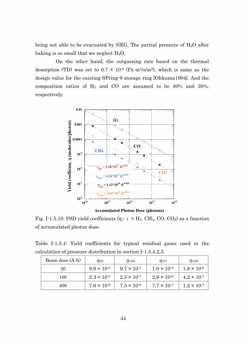
44
being not able to be evacuated by NEG. The partial pressure of H2O after baking is so small that we neglect H2O.
On the other hand, the outgassing rate based on the thermal desorption (TD) was set to 6.7 × 10⁻⁹ (Pa·m3/s/m2), which is same as the design value for the existing SPring-8 storage ring [Ohkuma1994]. And the composition ratios of H2 and CO are assumed to be 80% and 20%, respectively.
Fig. I-1.5.10: PSD yield coefficients (𝜂𝑖: 𝑖 = H2, CH4, CO, CO2) as a function of accumulated photon dose.
Table I-1.5.4: Yield coefficients for typical residual gases used in the calculation of pressure distribution in section I-1.5.4.2.3.
Beam dose (A·h) ηH2 ηCH4 ηCO ηCO2
20 8.6 × 10⁻⁵ 9.7 × 10⁻⁷ 1.0 × 10⁻⁵ 1.8 × 10⁻⁶ 100 2.3 × 10⁻⁵ 2.5 × 10⁻⁷ 2.6 × 10⁻⁶ 4.2 × 10⁻⁷ 400 7.6 × 10⁻⁶ 7.5 × 10⁻⁸ 7.7 × 10⁻⁷ 1.2 × 10⁻⁷
45
I-1.5.4.2.2. Arrangement of Vacuum Pumps A suitable arrangement of pumping systems was examined so as to
keep the τg at about 60 h at 100 mA after a beam dose of 400 A·h. This in turn means that it will be necessary to operate at a lower beam current or operate with a shorter τg in the early stage of the commissioning. NEG and SIP will be arranged at all the CR and AB where the PSD should be excited. Four different pumping systems with a combination of pumping speed for each residual gas are arranged, as specified in Table I-1.5.5. Expecting the SIP to evacuate only CH4, we selected relatively small-sized one. Although we have a plan to insert distributed ion pump (DIP) into the BSC near the BCA to increase evacuating ability of CH4, the pumping speed of DIP was not taken into account. We are ready to re-activate all the NEG cartridges when the beam dose reaches about 20 A·h in order to restore the pumping ability when the deterioration of the effective pumping speed is recognized beyond the accumulated beam dose of 20 A·h.
Conductance of each vacuum chamber calculated for each residual gas is used for the pressure calculation.
Table I-1.5.5: Assumed pumping speed and position. Pumping system
H2
(m3/s) CH4
(m3/s) CO (m3/s)
CO2 (m3/s)
Position
1 0.36 0.01 0.17 0.10 CR1, 2, AB1, 2, 3, 4, 6, 7, BCA4
2 0.12 0.01 0.05 0.03 AB8, BCA1, 3 3 0.47 0.01 0.22 0.13 AB5 4 0.23 0.01 0.1 0.06 BCA2, 5
I-1.5.4.2.3. Pressure Distribution and Beam Lifetime Using the outgassing rate, pumping speed and conductance
mentioned above, partial pressures for each residual gas were calculated. Figures I-1.5.11 and I-1.5.12 show the expected pressure distributions per unit cell except ID section at 100 mA when the beam doses reach 20 A·h and

46
400 A·h, respectively. The average pressures of each gaseous species are PH2 = 1.2 × 10⁻⁶ (1.3 × 10⁻⁷), PCH4 = 2.9 × 10⁻⁷ (2.3 × 10⁻⁸), PCO = 4.1 × 10⁻⁷ (5.3 × 10⁻⁸) and PCO2 = 8.7 × 10⁻⁸ (5.8 × 10⁻⁹) Pa by the photon stimulated desorption and the thermal desorption with the stored beam current of 100 mA at beam dose of 20 A·h (400 A·h). The each gas scattering lifetime is estimated from the average pressure of each gaseous species using the relationship of Table I-1.5.3. Then, the overall τg in a unit cell was calculated using the following equation,
1𝜏𝑔
= ∑ 1𝜏𝑔𝑖
𝑖 .
i= H2, CH4, CO and CO2 (I-1.5.5)
In this way, at a beam dose of 20 A·h, the τg was estimated at 6.6 h
resulting in the τtotal of 4.3 h derived from equation (I-1.5.1). Even if ID gap is closed to 5 mm, they just slightly decrease to 5.7 h and 3.8 h, respectively.
Typical results are summarized in Table I-1.5.6 and all the results are shown in Fig. I-1.5.13. As a matter of course, the lifetime increases with increasing beam dose. When the beam dose reaches 400 A·h, the τg will reach 62 h, which exceeds our target of 60 h. It will indeed decrease to 54 h when ID gap is closed to 5 mm, but this reduction has little influence on the τtotal. Furthermore, when the beam dose reaches 1000 A·h, as the τg will reach about 100 h even at an ID gap of 5 mm, which is more than seven times the τT of 12 h, it can be said that the τg has no impact on the τtotal. Consequently, it is confirmed that the targeted τg can be achieved by the assumed vacuum pumping system.

47
Fig. I-1.5.11: Expected pressure distribution in a unit cell with the stored beam current of 100 mA at beam dose of 20 A·h.
Fig. I-1.5.12: Expected pressure distribution in a unit cell with the stored beam current of 100 mA at beam dose of 400 A·h.

48
Fig. I-1.5.13: The gas scattering lifetime and the total beam lifetime with the stored beam current of 100 mA as a function of the beam dose. Average pressure at 100 mA is also shown here. Table I-1.5.6: Calculation results of the gas scattering lifetime and the beam lifetime with the average pressure for beam doses of 20, 100 and 400 A·h. GFO means that ID gap is fully opened.
Beam dose (A·h)
Average pressure (Pa)
τg (h) τtotal (h)
ID gap
GFO
ID gap
5 mm
ID gap
GFO
ID gap
5 mm
20 2.0 × 10⁻⁶ 6.6 5.7 4.3 3.8 100 5.5 × 10⁻⁷ 24 21 8.0 7.6 400 2.1 × 10⁻⁷ 62 54 10 9.8

49
I-1.5.5. Vacuum Components I-1.5.5.1. UHV Pump
We are going to select discrete NEG cartridges integrated into CF flanges as main UHV pumps to increase maintainability. Small-sized SIPs will also be installed for the evacuation of CH4, which cannot be evacuated by NEG pumps. And, insertion of the DIP element into the BSC is under consideration. Distributed NEG strips, which have been used in the existing SPring-8 storage ring, could not be installed inside the antechamber because they would interfere with synchrotron radiation due to the smallness of the chamber. The vacuum conductance of the chamber is so small that small-sized NEG cartridges will be installed nearby every photon absorbers. Half a year after the first commissioning stage, we plan to conduct re-activation of all the NEG cartridges in a shortest possible period within a month. In these days, NEG coating chamber has come to be employed in some synchrotron radiation facilities [Herbeaux2008], because it works effectively for a small chamber with low vacuum conductance. However, it would inevitably lead us to re-activate entire vacuum chambers composing the 1.5 km storage ring resulting in unacceptable enormous time for the activation procedure. In addition, we are concerned that it has essentially low sorption capacity so that the pumping ability would decrease in a short period of time [Benvenuti2001], [Bender2010], followed by frequent re-coating would be necessary compared with the NEG cartridges. Furthermore, according to the pressure distribution estimation (see section I-1.5.4), it was confirmed that enough ultimate pressure for the ultra low emittance ring with the top-up operation could be achieved by arranging local pumping systems effectively nearby all the photon absorbers. Therefore, we are negative about adapting NEG coating chambers to the new machine. I-1.5.5.2. Roughing Pump
Existing vacuum pump units in our facility, each of which consists of a turbo molecular pump (TMP) of 0.25 m3/s and a scroll pump, will be
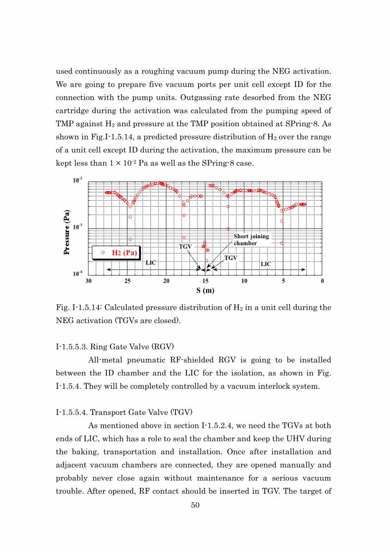
50
used continuously as a roughing vacuum pump during the NEG activation. We are going to prepare five vacuum ports per unit cell except ID for the connection with the pump units. Outgassing rate desorbed from the NEG cartridge during the activation was calculated from the pumping speed of TMP against H2 and pressure at the TMP position obtained at SPring-8. As shown in Fig.I-1.5.14, a predicted pressure distribution of H2 over the range of a unit cell except ID during the activation, the maximum pressure can be kept less than 1 × 10⁻² Pa as well as the SPring-8 case.
Fig. I-1.5.14: Calculated pressure distribution of H2 in a unit cell during the NEG activation (TGVs are closed). I-1.5.5.3. Ring Gate Valve (RGV)
All-metal pneumatic RF-shielded RGV is going to be installed between the ID chamber and the LIC for the isolation, as shown in Fig. I-1.5.4. They will be completely controlled by a vacuum interlock system. I-1.5.5.4. Transport Gate Valve (TGV)
As mentioned above in section I-1.5.2.4, we need the TGVs at both ends of LIC, which has a role to seal the chamber and keep the UHV during the baking, transportation and installation. Once after installation and adjacent vacuum chambers are connected, they are opened manually and probably never close again without maintenance for a serious vacuum trouble. After opened, RF contact should be inserted in TGV. The target of
51
designing the TGV is miniaturization and weight reduction with simple configuration. I-1.5.5.5. Bellows
Bellows with the RF shielding will be arranged at both ends of the BSC, and near the BPM. Both aluminum formed bellows and stainless steel welded bellows are under consideration. We will make a decision based on the R&D results, because innovative miniaturization is required. I-1.5.6. Light Extraction Design
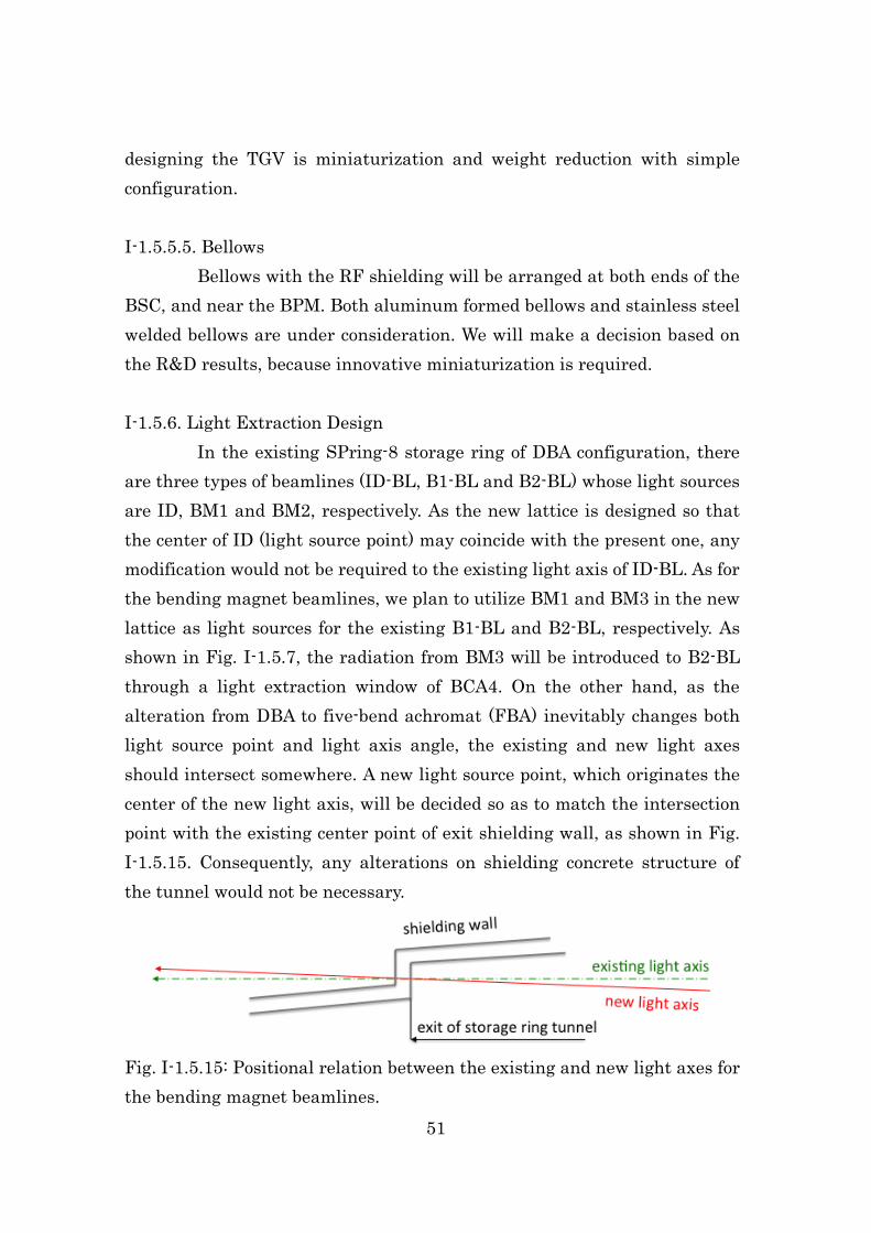
In the existing SPring-8 storage ring of DBA configuration, there are three types of beamlines (ID-BL, B1-BL and B2-BL) whose light sources are ID, BM1 and BM2, respectively. As the new lattice is designed so that the center of ID (light source point) may coincide with the present one, any modification would not be required to the existing light axis of ID-BL. As for the bending magnet beamlines, we plan to utilize BM1 and BM3 in the new lattice as light sources for the existing B1-BL and B2-BL, respectively. As shown in Fig. I-1.5.7, the radiation from BM3 will be introduced to B2-BL through a light extraction window of BCA4. On the other hand, as the alteration from DBA to five-bend achromat (FBA) inevitably changes both light source point and light axis angle, the existing and new light axes should intersect somewhere. A new light source point, which originates the center of the new light axis, will be decided so as to match the intersection point with the existing center point of exit shielding wall, as shown in Fig. I-1.5.15. Consequently, any alterations on shielding concrete structure of the tunnel would not be necessary.
Fig. I-1.5.15: Positional relation between the existing and new light axes for the bending magnet beamlines.

52
References [Anashin1998] V. Anashin et al., Proc. of the European Particle Accelerator Conference 1998, Stockholm, Sweden, (2008) pp. 2163-2165. [Bender2010] M. Bender et al., J. Nuclear Instruments and Method in Physics Research B268 (2010) pp. 1986-1990. [Benvenuti2001] C. Benvenuti et al., Vacuum 60 (2001) pp. 57-65. [Gröbner1994] O. Gröbner, et al., J. Vac.Sci. Technol A12(3), May, Jun 1994, pp.846-853. [Herbeaux2008] C. Herbeaux, et al., Proc. of the European Particle Accelerator for Conference 2008, Genoa, Italy, (2008) pp. 3696-3698. [Ohkuma1994] H. Ohkuma, et al., Proc. 9th Meeting on Ultra High Vacuum Techniques Accelerators and Storage Rings, KEK, Jpn., (1994), pp. 29-45. [Oishi2014] M. Oishi, et al., submitted to J. Vac. Soc. Jpn. (in Japanese). [Takahashi2008] S. Takahashi, et al., J. Synchrotron Rad. 15, (2008) 144-150.

53
I-1.6. RF System I-1.6.1. Introduction
The role of an RF acceleration system of a storage ring is to generate a sufficient beam-accelerating voltage and compensate for beam-energy loss caused by synchrotron radiation in bending magnets and insertion devices. The RF system of the SPring-8 storage ring has stably generated a voltage of 16 MV at a frequency of 508.58 MHz and accelerated an electron beam with a current of 100 mA since 1997 for synchrotron-radiation users. The necessary RF power is generated by klystrons in four RF stations and supplied to 32 bell-shaped single-cell cavities in the straight sections of the SPring-8 storage ring [Kawashima2008].
Table I-1.6.1 shows the parameters related to the RF system of the SPring-8-II. In upgrading the storage ring for the SPring-8-II, a beam energy is lowered to 6 GeV and energy losses by radiation in bending magnets and insertion devices are 3 MeV/turn and 2 MeV/turn, respectively. In consequence, a needed RF voltage decreases to 7 MV. Since the strength of radiation damping is weakened, we should be careful as to instabilities arising from parasitic impedances of cavities.
Since the momentum compaction factor exchanges the beam energy with the longitudinal beam position, the energy and the position become sensitive to the amplitude, phase, and frequency changes of the RF system. Hence, the stability of the acceleration RF field is also important for the SPring-8-II storage ring. We set requirements for the stabilities of the beam energy and the longitudinal beam position to < 1 × 10⁻⁴ and < 1 ps, respectively, which are well below the natural energy spread and the natural bunch length in Table I-1.6.1. From these requirements, the demanded stability for the acceleration RF field is derived, as listed in Table I-1.6.2. Thus, a precise low-level RF (LLRF) system to regulate the RF voltage and phase in the acceleration cavity is indispensable.
Taking these demands and upgrading cost-effectiveness into account, the present high-power RF components with the excellent

54
performance and durability are reused for the next high-power RF system. Although the performance of the present LLRF system is comparable to the requirement, the design of the present LLRF system is out-of-date and the electronic components are hard to maintain. Therefore, an entirely new digital LLRF system is designed to improve the stability in beam acceleration and to handle a low-emittance beam precisely.
Table I-1.6.1: Parameters of the SPring-8-II RF system.
Beam energy 6 GeV Beam current 100 mA Beam accelerating frequency 508.762 MHz Radiation energy loss per turn 5.0 MeV in bending magnets 3.0 MeV in insertion devices 2.0 MeV Beam accelerating voltage 7 MV Circumference 1435.43 m Harmonic number 2436 Beam revolution frequency 208.851 kHz Over-voltage ratio 1.4 Natural energy spread (∆E/E) 0.093% Synchrotron frequency 670 Hz Betatron function at the cavity position Horizontal Vertical
5.50 m 3.00 m
Momentum compaction factor 3.27×10⁻⁵ Bunch length 6 ps rms
RF stations 4 RF cavities 16 Shunt impedance of the bell-shaped cavity 6 MΩ Total wall loss in cavities 510 kW Beam loading power 500 kW

55
Table I-1.6.2: Requirements for the SPring-8-II RF system.
I-1.6.2. High-Power RF System I-1.6.2.1. Configuration of High-Power RF Components
An energy loss by radiation is up to 5 MeV/turn and the maximal power to beam loading is 500 kW at a beam current of 100 mA. We need an accelerating voltage of 7 MV in order to compensate the losses and have a sufficient quantum lifetime. Since the SPring-8-II employs multi-bending optics, the straight sections available for the cavities are about 20% shorter than those of the present storage ring. The number of RF cavities in the sections is reduced to half and the existing RF system is rearranged into one driving four cavities in each station. The 16 cavities consume an RF power of 510 kW to generate the accelerating voltage. The RF system with the four stations is so redundant that the beam acceleration of 7 MV can continue by raising RF power of the three stations by 55% in case one station fails.
The plan of using six cavities in one section or the total of 18 cavities has also been investigated to carry out the acceleration with three RF stations. This plan is also redundant against one station failure. However, it is barely capable to install the six cavities with incidental equipment such as vacuum chambers and further shorting the sections by change in optics design or other ring components is difficult to be accepted. Thus we employ the four-station system affording to install 16 cavities and having the redundancy described above.
Accelerating voltage stability and AM noise (Integral of DC – 200kHz)
< 1 × 10⁻³
Phase stability and phase noise (Integral of DC – 200kHz)
< 0.1 degree
Phase noise and AM noise at the offset frequency near the synchrotron frequency
< -100 dBc/Hz
Accelerating frequency stability < 3 × 10⁻⁹
56
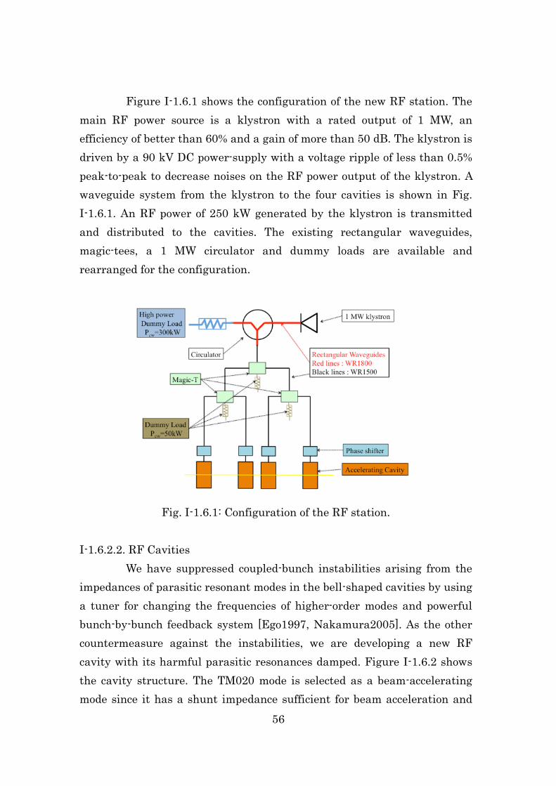
Figure I-1.6.1 shows the configuration of the new RF station. The main RF power source is a klystron with a rated output of 1 MW, an efficiency of better than 60% and a gain of more than 50 dB. The klystron is driven by a 90 kV DC power-supply with a voltage ripple of less than 0.5% peak-to-peak to decrease noises on the RF power output of the klystron. A waveguide system from the klystron to the four cavities is shown in Fig. I-1.6.1. An RF power of 250 kW generated by the klystron is transmitted and distributed to the cavities. The existing rectangular waveguides, magic-tees, a 1 MW circulator and dummy loads are available and rearranged for the configuration.
Fig. I-1.6.1: Configuration of the RF station.
I-1.6.2.2. RF Cavities We have suppressed coupled-bunch instabilities arising from the
impedances of parasitic resonant modes in the bell-shaped cavities by using a tuner for changing the frequencies of higher-order modes and powerful bunch-by-bunch feedback system [Ego1997, Nakamura2005]. As the other countermeasure against the instabilities, we are developing a new RF cavity with its harmful parasitic resonances damped. Figure I-1.6.2 shows the cavity structure. The TM020 mode is selected as a beam-accelerating mode since it has a shunt impedance sufficient for beam acceleration and

57
brings a compact damping structure to the cavity. The estimated shunt impedance and unloaded Q are 6.8 MΩ and 60,300, respectively. The cavity has two slots along the magnetic node of the TM020 mode and materials absorbing RF waves are fitted in them. Though the TM020 mode is insensible to the slots, the parasitic resonances have electromagnetic fields intruding into them and are damped sufficiently. Figure I-1.6.3 shows the estimated impedance distributions of all the monopole and dipole modes trapped in the cavity. The impedances of parasitic modes are reduced and less than the thresholds of the instabilities.
Fig. I-1.6.3: Impedance distributions of resonant modes trapped into the cavity calculated with MAFIA: (a) monopoles and (b) dipoles. The solid redlines show the thresholds of the instabilities. I-1.6.2.3. Solid-State Amplifier Option
Thanks to a recent progress of the semiconductor technology, hundred-kW class solid-state amplifiers (SSA) in an UHF frequency band were fabricated in several accelerator facilities and companies [Marchand2007, Pardine2012, Jacob2013, Broere2011]. The SSA is an
Fig. I-1.6.2: RF cavity with its harmful parsitic resonances damped.
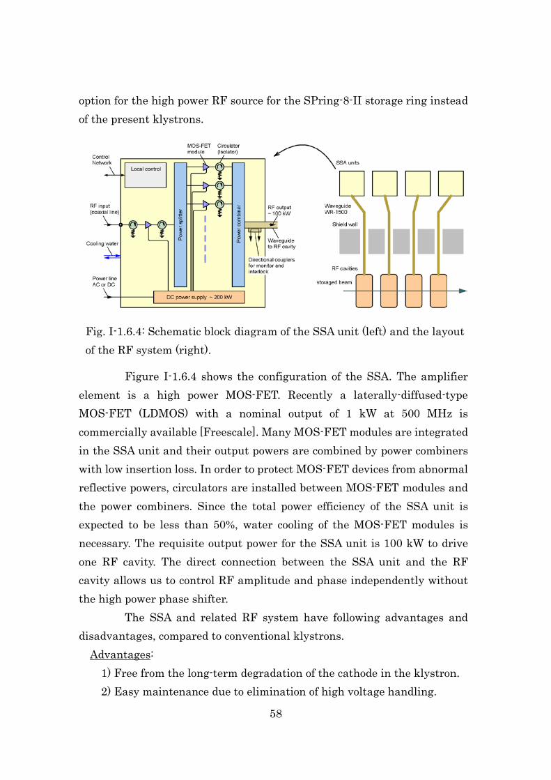
58
option for the high power RF source for the SPring-8-II storage ring instead of the present klystrons.
Figure I-1.6.4 shows the configuration of the SSA. The amplifier element is a high power MOS-FET. Recently a laterally-diffused-type MOS-FET (LDMOS) with a nominal output of 1 kW at 500 MHz is commercially available [Freescale]. Many MOS-FET modules are integrated in the SSA unit and their output powers are combined by power combiners with low insertion loss. In order to protect MOS-FET devices from abnormal reflective powers, circulators are installed between MOS-FET modules and the power combiners. Since the total power efficiency of the SSA unit is expected to be less than 50%, water cooling of the MOS-FET modules is necessary. The requisite output power for the SSA unit is 100 kW to drive one RF cavity. The direct connection between the SSA unit and the RF cavity allows us to control RF amplitude and phase independently without the high power phase shifter.
The SSA and related RF system have following advantages and disadvantages, compared to conventional klystrons. Advantages: 1) Free from the long-term degradation of the cathode in the klystron. 2) Easy maintenance due to elimination of high voltage handling.
Fig. I-1.6.4: Schematic block diagram of the SSA unit (left) and the layout of the RF system (right).

59
3) High modularity of the amplifier elements associated with redundancy and flexibility for the required RF power changes.
Disadvantages: 4) Low power efficiency less than 50 % for class-AB amplifier and the
resultant high operational cost. Improvement of the power efficiency should be studied with introducing the other class operation such as class-D.
5) High cost for development and production of the SSA, modification of electrical power lines and the cooling water system.
I-1.6.3. Low-Level RF System
The low-level RF (LLRF) system is demanded to have following functions in order to stabilize the phase and amplitude of the accelerating RF field. 1) Generate an appropriate RF signal for the klystron from a reference RF
signal. 2) Detect RF signals in the RF cavity and the waveguide precisely. 3) Control a RF cavity tuner and a klystron anode power supply. 4) Construct an optimum feedback loop among these functions.
Some of the requirements for the LLRF system are already shown in Table I-1.6.2. Although these requirements can be satisfied by the present LLRF system, the present system consists of out-of-date components, such as a diode amplitude detector, a mixer phase detector, and an analog feedback loop. Therefore, we are developing a new digital LLRF system with modern RF modulation/detection technique and a digital feedback loop. Since the number of analog components in the digital LLRF system is small, environmental perturbations, such as temperature drift, can be reduced. The digital LLRF system also has high adaptability to a modern digital feedback control.
Figure I-1.6.5 shows a schematic diagram of the digital LLRF system at each RF station. The reference RF signal is modulated by an IQ modulator and the RF signal is fed into the klystron. RF signals from the klystron output, the RF cavity input, the pickup of an RF cavity, etc. are
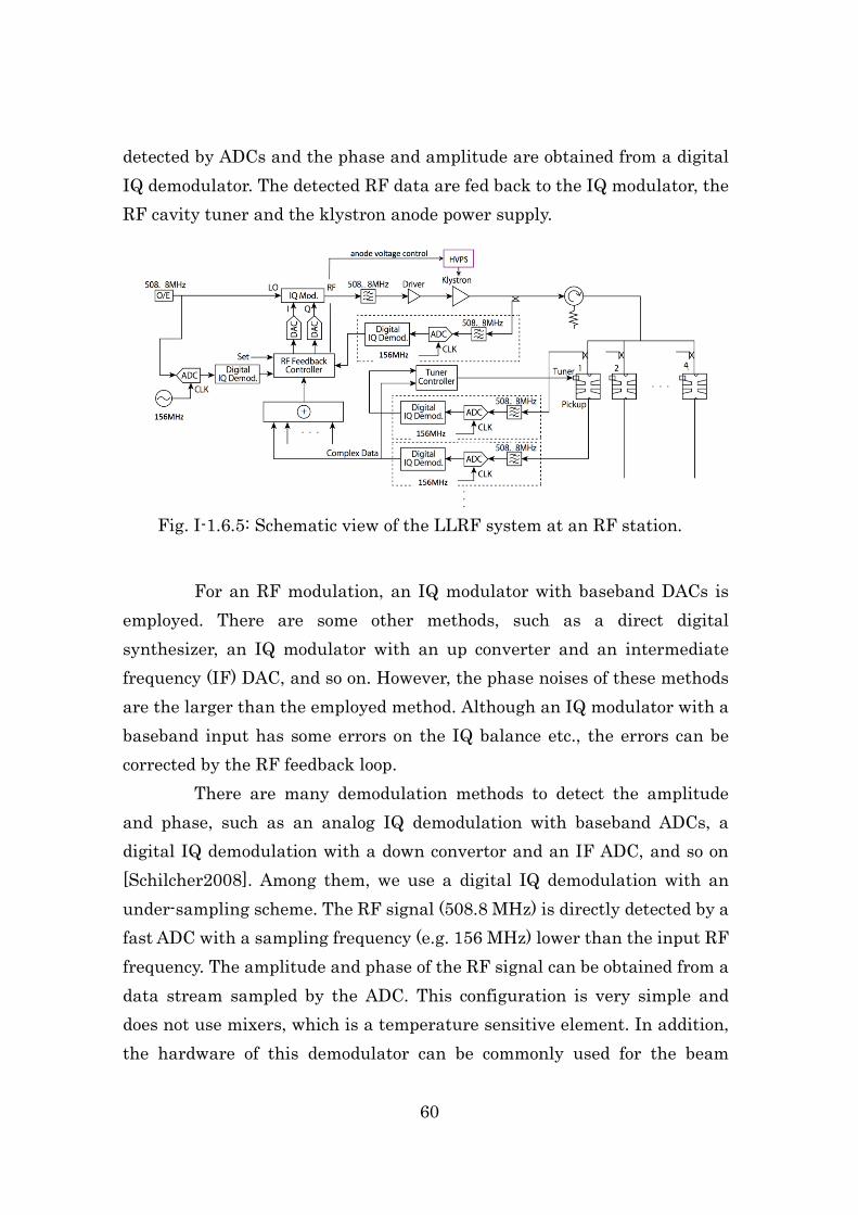
60
detected by ADCs and the phase and amplitude are obtained from a digital IQ demodulator. The detected RF data are fed back to the IQ modulator, the RF cavity tuner and the klystron anode power supply.
For an RF modulation, an IQ modulator with baseband DACs is
employed. There are some other methods, such as a direct digital synthesizer, an IQ modulator with an up converter and an intermediate frequency (IF) DAC, and so on. However, the phase noises of these methods are the larger than the employed method. Although an IQ modulator with a baseband input has some errors on the IQ balance etc., the errors can be corrected by the RF feedback loop.
There are many demodulation methods to detect the amplitude and phase, such as an analog IQ demodulation with baseband ADCs, a digital IQ demodulation with a down convertor and an IF ADC, and so on [Schilcher2008]. Among them, we use a digital IQ demodulation with an under-sampling scheme. The RF signal (508.8 MHz) is directly detected by a fast ADC with a sampling frequency (e.g. 156 MHz) lower than the input RF frequency. The amplitude and phase of the RF signal can be obtained from a data stream sampled by the ADC. This configuration is very simple and does not use mixers, which is a temperature sensitive element. In addition, the hardware of this demodulator can be commonly used for the beam
Fig. I-1.6.5: Schematic view of the LLRF system at an RF station.
61
position monitor electronics. Since a required RF amplitude stability is 1 × 10⁻³, the ADC is needed to have a resolution of 1 × 10⁻⁴, corresponding to a 16-bit level. Furthermore, an ADC clock jitter should be as small as 100 fs. This performance can be achieved by the present ADC technology, such as a 16-bit ADC module utilized in SACLA.
Perturbation sources to the amplitude and phase of an RF field in the cavity are the ripple of a klystron high voltage power supply (HVPS), a change of the electrical length of the waveguide between the klystron and the cavity, a change of the cavity resonant frequency by a cavity temperature change, a drift of the IQ modulator and so on. A noise component with an offset frequency higher than several 10 kHz is suppressed by the bandwidth of the accelerating cavity [Ego1996]. There are two feedback control loops to stabilize the amplitude and phase of the cavity. The first one is a klystron loop and it suppresses the ripple caused by the HVPS for the klystron, etc. The bandwidth of the klystron loop is several kHz. The second one is a cavity loop to suppress the effect from the temperature drift, etc. The bandwidth of the cavity loop is several 10 Hz. The response time of the feedback loop can be optimized by software modification of adjusting the bandwidth of a digital filter with balancing a noise level.
In addition to the stabilization of the acceleration RF field, we implement a suppression function of coherent synchrotron oscillation to the LLRF system. A dedicated feedback system to suppress the coherent synchrotron oscillation is in operation at the present storage ring [Ohshima2001]. This system will be upgraded for the SPring-8-II storage ring. A signal from the beam position monitor is transferred to the LLRF system, and an appropriate RF signal to suppress the coherent synchrotron oscillation is generated. Since the synchrotron frequency of the new storage ring is near the harmonics of the power line cycle (720Hz), the influence from the ripple of the klystron HVPS can be large. Even if such an effect exists, coherent synchrotron oscillation can be sufficiently reduced by this suppression scheme.
62
I-1.6.4. Synchronization and Timing
Since RF stations and other RF electronics are distributed along the storage ring, a reference RF signal of 508.8 MHz is demanded to be delivered to the RF electronics. The phase stability of the acceleration RF signal is required to be less than 1 ps, which is small enough compared to a bunch length of 6 ps. Therefore, a low-noise master oscillator and a stable RF distribution system are necessary for the synchronization between RF stations. A revolution signal of 208.85 kHz is also needed to be distributed together with a reference RF signal in order to trigger the electronics. In addition, SACLA is newly shared as an injector instead of the booster synchrotron of SPring-8. We need the pulse-by-pulse synchronization between the storage ring and SACLA, since a low-emittance and ultra-short pulse-width beam produced by SACLA must be conveyed and injected precisely to the storage ring with a small dynamic aperture.
I-1.6.4.1. Master Oscillator
The reference RF signal of an accelerating frequency is supplied from a master oscillator located at the E station. Requirements for the oscillator are as follows; 1) High frequency stability and a resolution of Δf/f < 3x10⁻⁹ to maintain the stored beam energy within one tenth of the natural energy spread. 2) Large tuning range of Δ f/f > 10-6 to cope with a change of the circumference caused by a seasonal change of ground temperature (~7x10⁻⁷/year [Takao2000]) and by the daily tidal deformation (~10-8/day [Date1999]). 3) Low SSB phase noise near the synchrotron frequency not to excite large coherent synchrotron oscillation. (< -100 dBc/Hz around an offset frequency of 670 Hz) The signal generator used at the present storage ring has a frequency stability of better than 10-10 and satisfies all the requirements. Therefore, the present signal generator is a candidate for the next ring.

63
I-1.6.4.2. Distribution of the Reference RF Signal The reference RF signal is delivered to four RF stations, several
tens of beam position monitor units and some synchrotron radiation users located along the ring. The optical transmission scheme is selected because of low transmission loss compared to that of a coaxial cable, and its electrical isolation capability between the RF stations. The allowance of the phase drift between the RF stations is set to be 1 ps. To reduce thermal optical fiber length drift, therefore, we use a phase-stabilized optical fiber (< 5 ps/km/K).
For connections from an optical transmitter to optical receivers for transmitting the reference RF signals, a bus topology or a star topology is commonly used for a network system. For the bus topology, the number of optical fibers can be reduced. However, the signal-to-noise (S/N) ratio is relatively small, since only a small portion of transmitted optical power at a brunched-off point using an optical coupler can be extracted to each receiver. Furthermore, optical power handled with one optical fiber is limited, because of non-linear response, where the power is over a certain threshold level. In this case, it is difficult to achieve the required phase noise and AM noise performance. In our case, therefore, a star topology is used because it has better S/N ratio by increasing the optical signal power at the receiver, as shown in Fig. I-1.6.6. In addition, the star topology has an ability to introduce an optical fiber length stabilization system as a future option.
Fig. I-1.6.6: A schematic view of the distribution system of reference and timing signals.
64
The revolution signal is generated by dividing the reference RF signal with the harmonic number and used to trigger the BPM electronics, the experimental apparatus of synchrotron radiation users and so on. The timing accuracy is required to be a few ps level, which is comparable to the reference RF signal. We use a Wavelength Division Multiplexing (WDM) based system, because it has a proved result of low time jitter of 5 ps p-p at SACLA [Otake2011].
I-1.6.4.3. Synchronization with SACLA
In order to inject an electron beam from SACLA to the SPring-8-II storage ring, the beam timing of SACLA must be synchronized with the desired bucket of the storage ring. In addition, the injection to the storage ring must be done in parallel with the SACLA user operation. Since beam parameters, such as a beam energy, a bunch charge and a bunch length are different between the injection and the SACLA operation, a pulse-by-pulse control system for changing the beam parameters conducted by changing machine conditions, such as RF phases, is required. In this section, we describe the synchronization scheme between the storage ring and SACLA and the pulse-by-pulse control system for SACLA.
I-1.6.4.3.1. Synchronization Scheme
The ratio between the acceleration frequency of the storage ring, 508.762 MHz, and the fundamental reference clock frequency of SACLA, 238 MHz, is 295/138. Therefore, if the RF phase of SACLA is locked to that of the storage ring, SACLA is synchronized with the storage ring at every 295 buckets (580 ns, corresponding to 1.72 MHz). Since the harmonic number, 2436, is relatively prime to 295, all the buckets can be synchronized with SACLA in 1.41 ms (= 580 ns x 2436). When a beam injection is requested by the storage ring, the SACLA accelerator is necessary to be triggered at appropriate timing for a desired bucket.
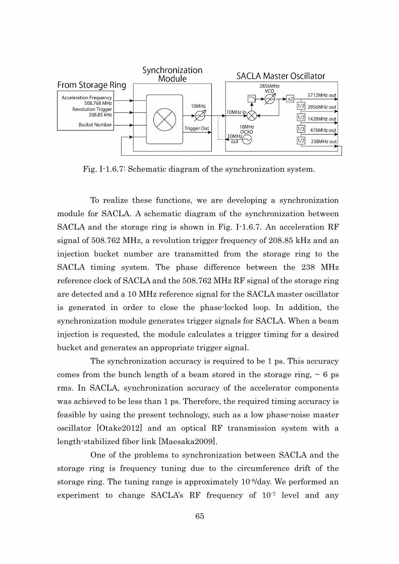
65
To realize these functions, we are developing a synchronization
module for SACLA. A schematic diagram of the synchronization between SACLA and the storage ring is shown in Fig. I-1.6.7. An acceleration RF signal of 508.762 MHz, a revolution trigger frequency of 208.85 kHz and an injection bucket number are transmitted from the storage ring to the SACLA timing system. The phase difference between the 238 MHz reference clock of SACLA and the 508.762 MHz RF signal of the storage ring are detected and a 10 MHz reference signal for the SACLA master oscillator is generated in order to close the phase-locked loop. In addition, the synchronization module generates trigger signals for SACLA. When a beam injection is requested, the module calculates a trigger timing for a desired bucket and generates an appropriate trigger signal.
The synchronization accuracy is required to be 1 ps. This accuracy comes from the bunch length of a beam stored in the storage ring, ~ 6 ps rms. In SACLA, synchronization accuracy of the accelerator components was achieved to be less than 1 ps. Therefore, the required timing accuracy is feasible by using the present technology, such as a low phase-noise master oscillator [Otake2012] and an optical RF transmission system with a length-stabilized fiber link [Maesaka2009].
One of the problems to synchronization between SACLA and the storage ring is frequency tuning due to the circumference drift of the storage ring. The tuning range is approximately 10-8/day. We performed an experiment to change SACLA’s RF frequency of 10-7 level and any
Fig. I-1.6.7: Schematic diagram of the synchronization system.
66
deterioration of X-ray laser intensity was not observed. Thus, the RF frequency of SACLA can follow the frequency shift of the storage ring by the tuning.
I-1.6.4.3.2. Pulse-by-Pulse Trigger and RF Control System for SACLA
In order to inject an electron beam to the storage ring in parallel with the SACLA user operation, we are developing a pulse-by-pulse trigger and RF control system. When this system receives an injection request during the SACLA operation, a certain trigger pulse for the SACLA operation is replaced with an injection trigger pulse. In addition, the injection trigger pulse is distributed to every accelerator unit of SACLA, and the acceleration RF amplitude and phase of the units are switched from the preset to appropriate values in time-sharing to the storage ring injection.
In order to switch the acceleration condition pulse-by-pulse, event information for each trigger pulse is demanded for the accelerator unit. Therefore, we considered following three methods for the event distribution.
1) Event code is transmitted together with the trigger pulse. 2) Event information is distributed with the existing Ethernet network. 3) Event information is distributed with a newly-built reflective memory
network. A schematic diagram of the method 1) is shown in Fig. I-1.6.8. The synchronization module, described in the previous section, generates the trigger pulse with the event code. The trigger signal is distributed to the Trigger Delay Unit (TDU) for each accelerator unit in SACLA. The TDU provides appropriate trigger pulses to accelerator components according to the event code. In addition, the TDU tells the event code to D/A and A/D converter boards for RF phase and amplitude control and the desired acceleration RF manipulation signal is generated.
The difference among the three methods is just a route of the event information. For the methods 1) and 2), no additional hardware is needed from the present trigger system situation. For the method 2), however, the latency of the Ethernet network strongly depends on a network traffic
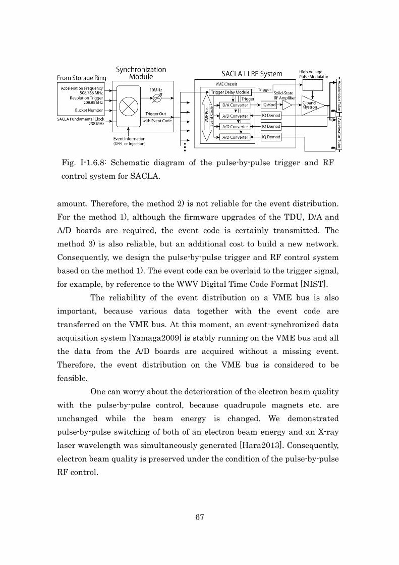
67
amount. Therefore, the method 2) is not reliable for the event distribution. For the method 1), although the firmware upgrades of the TDU, D/A and A/D boards are required, the event code is certainly transmitted. The method 3) is also reliable, but an additional cost to build a new network. Consequently, we design the pulse-by-pulse trigger and RF control system based on the method 1). The event code can be overlaid to the trigger signal, for example, by reference to the WWV Digital Time Code Format [NIST].
The reliability of the event distribution on a VME bus is also important, because various data together with the event code are transferred on the VME bus. At this moment, an event-synchronized data acquisition system [Yamaga2009] is stably running on the VME bus and all the data from the A/D boards are acquired without a missing event. Therefore, the event distribution on the VME bus is considered to be feasible.
One can worry about the deterioration of the electron beam quality with the pulse-by-pulse control, because quadrupole magnets etc. are unchanged while the beam energy is changed. We demonstrated pulse-by-pulse switching of both of an electron beam energy and an X-ray laser wavelength was simultaneously generated [Hara2013]. Consequently, electron beam quality is preserved under the condition of the pulse-by-pulse RF control.
Fig. I-1.6.8: Schematic diagram of the pulse-by-pulse trigger and RF control system for SACLA.

68
References [Broere2011] J. Broere, et. al., Proceedings of IPAC2011, MOPC137, (2011). [Date1999] S. Date, N. Kumagai, "A long-term observation of the DC component of the horizontal COD in the storage ring of SPring-8", Nuc. Instr. Meth. A421 (1999) 417-422. [Ego1996] H. Ego, et. al., Nucl. Instr. and Meth. A 383 (1996) pp. 325-336. [Ego1997] H. Ego, et al., Nucl. Instr. and Meth. A 400 (1997) p.195. [Freescale] For example, freescale MRFE6VP61K25H, http://www.freescale.com/ [Hara2013] T. Hara et al., Phys. Rev. ST Accel. and Beams, 16, 080701 (2013). [Jacob2013] J. Jacob, et. al., Proceedings of IPAC2013, WEPFI004, (2013). [Kawashima2008] Y. Kawashima, et. al., Proceedings of the 11th EPAC, Genoa (2008) p.1485. [Maesaka2009] H. Maesaka et al., Proceedings of ICALEPCS’09, 85-89 (2009). [Marchand2007] P. Marchand, et. al., Phys. Rev. ST Accel. and Beams, 10, 112001, (2007). [Nakamura2005] T. Nakamura and K. Kobayashi, Proceedings of ICALEPCS’05, PO2.022-2, (2005). [NIST] http://www.nist.gov/pml/div688/grp40/wwv.cfm [Ohshima2001] T. Ohshima and N. Kumagai, "Suppression of Coherent Synchrotron Oscillation of the SPring-8 Storage Ring", Proc. of PAC2001, p.1975-1977. [Otake2011] Y. Otake, "State-of-the-Art RF Distribution and Synchronization Techniques", Proc. of FEL2011, p.633-640. [Otake2012] Y. Otake et al., Nucl. Instrum. Meth. A 696, 151-163 (2012). [Pardine2012] C. Pardine, et. al., Proceedings of IPAC2012, THPPC052, (2012). [Schilcher2008] T. Schilcher, "RF applications in digital signal processing", Proceedings of CERN Accelerator School 2007, Sigtuna, Sweden p.249-283. [Takao2000] M. Takao T. Shimada, "Long Term Variation of the Circumference of the SPring-8 Storage Ring", Proc. of EPAC2000, p.

69
1572-1574. [Yamaga2009] M. Yamaga et al., Proceedings of ICALEPCS’09, 69-71 (2009).
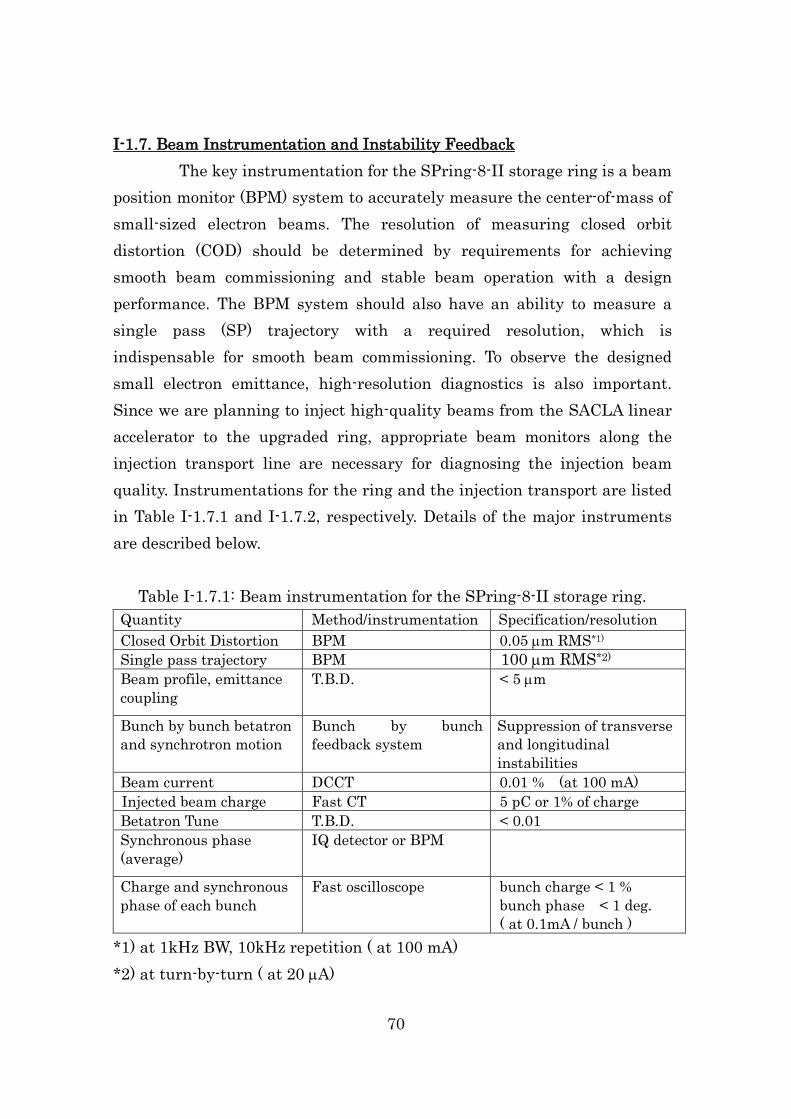
70
I-1.7. Beam Instrumentation and Instability Feedback The key instrumentation for the SPring-8-II storage ring is a beam
position monitor (BPM) system to accurately measure the center-of-mass of small-sized electron beams. The resolution of measuring closed orbit distortion (COD) should be determined by requirements for achieving smooth beam commissioning and stable beam operation with a design performance. The BPM system should also have an ability to measure a single pass (SP) trajectory with a required resolution, which is indispensable for smooth beam commissioning. To observe the designed small electron emittance, high-resolution diagnostics is also important. Since we are planning to inject high-quality beams from the SACLA linear accelerator to the upgraded ring, appropriate beam monitors along the injection transport line are necessary for diagnosing the injection beam quality. Instrumentations for the ring and the injection transport are listed in Table I-1.7.1 and I-1.7.2, respectively. Details of the major instruments are described below.
Table I-1.7.1: Beam instrumentation for the SPring-8-II storage ring. Quantity Method/instrumentation Specification/resolution Closed Orbit Distortion BPM 0.05 µm RMS*1) Single pass trajectory BPM 100 µm RMS*2) Beam profile, emittance coupling
T.B.D. < 5 µm
Bunch by bunch betatron and synchrotron motion
Bunch by bunch feedback system
Suppression of transverse and longitudinal instabilities
Beam current DCCT 0.01 % (at 100 mA) Injected beam charge Fast CT 5 pC or 1% of charge Betatron Tune T.B.D. < 0.01 Synchronous phase (average)
IQ detector or BPM
Charge and synchronous phase of each bunch
Fast oscilloscope bunch charge < 1 % bunch phase < 1 deg. ( at 0.1mA / bunch )
*1) at 1kHz BW, 10kHz repetition ( at 100 mA) *2) at turn-by-turn ( at 20 µA)
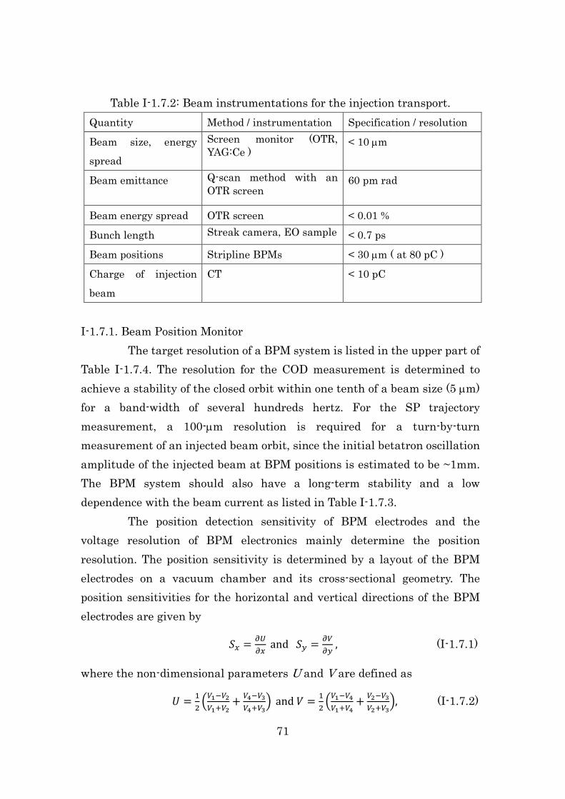
71
Table I-1.7.2: Beam instrumentations for the injection transport. Quantity Method / instrumentation Specification / resolution
Beam size, energy spread
Screen monitor (OTR, YAG:Ce )
< 10 µm
Beam emittance Q-scan method with an OTR screen
60 pm rad
Beam energy spread OTR screen < 0.01 %
Bunch length Streak camera, EO sample < 0.7 ps
Beam positions Stripline BPMs < 30 µm ( at 80 pC )
Charge of injection
beam
CT < 10 pC
I-1.7.1. Beam Position Monitor The target resolution of a BPM system is listed in the upper part of
Table I-1.7.4. The resolution for the COD measurement is determined to achieve a stability of the closed orbit within one tenth of a beam size (5 µm) for a band-width of several hundreds hertz. For the SP trajectory measurement, a 100-µm resolution is required for a turn-by-turn measurement of an injected beam orbit, since the initial betatron oscillation amplitude of the injected beam at BPM positions is estimated to be ~1mm. The BPM system should also have a long-term stability and a low dependence with the beam current as listed in Table I-1.7.3.
The position detection sensitivity of BPM electrodes and the voltage resolution of BPM electronics mainly determine the position resolution. The position sensitivity is determined by a layout of the BPM electrodes on a vacuum chamber and its cross-sectional geometry. The position sensitivities for the horizontal and vertical directions of the BPM electrodes are given by
𝑆𝑥 = 𝜕𝑈𝜕𝑥
and 𝑆𝑦 = 𝜕𝑉𝜕𝑦
, (I-1.7.1)
where the non-dimensional parameters U and V are defined as
𝑈 = 12�𝑉1−𝑉2𝑉1+𝑉2
+ 𝑉4−𝑉3𝑉4+𝑉3
� and 𝑉 = 12�𝑉1−𝑉4𝑉1+𝑉4
+ 𝑉2−𝑉3𝑉2+𝑉3
�, (I-1.7.2)
72
with the four signal voltages V1, V2, V3 and V4 from the electrodes. By using measured voltages and the position sensitivities, the horizontal and vertical beam positions are calculated as 𝑥 = 1 𝑆𝑥⁄ 𝑈 and 𝑦 = 1 𝑆𝑦⁄ 𝑉. As a result, the position resolution of the BPM system can be determined from these equations.
Table I-1.7.3: Features of the BPM system. Property Quantity Condition
Beam current dependence < 5 µm from 0.1 mA to 100 mA of stored beam current
Long-term stability < 5 µm for weeks Accuracy with respect to the centers of neighboring quadrupole / sextupole magnets
< 100 µm N.A.
I-1.7.1.1. BPM Electrode The geometrical dimension of a vacuum chamber of the SPring-8-II
storage ring is shown in Fig. I-1.7.1 and its vertical aperture is 16 mm. The “shorted-stripline” type electrode [Nakamura2005A] of the BPM could be selected, since larger signal strength at a detection frequency of 508 MHz can be expected over a conventional round-shape button type. In Fig. I-1.7.1, an example of the electrode under study is schematically shown. In the figure, the length, the width of the electrode, the gap between the electrode and the chamber, the horizontal separation of each electrode are 25 mm, 5 mm, 1 mm and 10 mm, respectively. The position sensitivities of the BPM electrodes are calculated as 0.14 / mm for both the horizontal and vertical directions. Then a signal-to-noise ratio (SNR) of 30 dB is required for the SP trajectory measurement and 96 dB is demanded for the COD measurement, in order to achieve the target resolution.
As for the SP trajectory measurement at a beam current of 20 µA, the SNR is determined by a signal strength detected with the BPM electrode. With this electrode, a signal strength of 10 dB larger than that of the button-type is expected. Similarly, a signal strength of -5 dBm is expected for the COD measurement at a stored beam current of 100 mA. These values are calculated by numerical simulations based on the above-mentioned equations and by using the geometrical dimension.
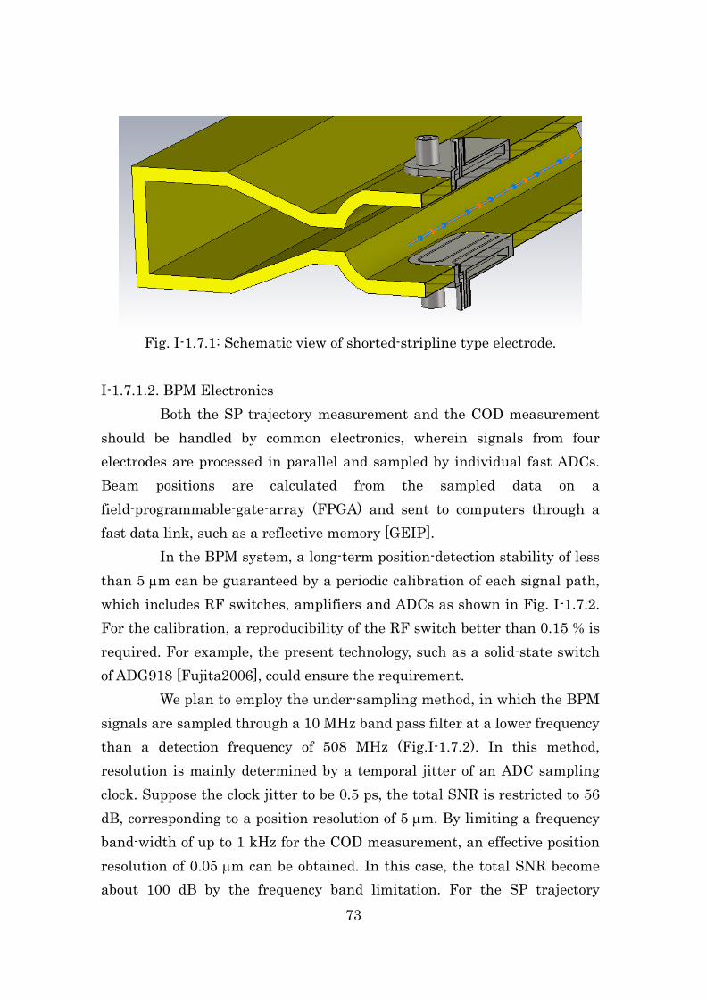
73
Fig. I-1.7.1: Schematic view of shorted-stripline type electrode.
I-1.7.1.2. BPM Electronics Both the SP trajectory measurement and the COD measurement
should be handled by common electronics, wherein signals from four electrodes are processed in parallel and sampled by individual fast ADCs. Beam positions are calculated from the sampled data on a field-programmable-gate-array (FPGA) and sent to computers through a fast data link, such as a reflective memory [GEIP].
In the BPM system, a long-term position-detection stability of less than 5 µm can be guaranteed by a periodic calibration of each signal path, which includes RF switches, amplifiers and ADCs as shown in Fig. I-1.7.2. For the calibration, a reproducibility of the RF switch better than 0.15 % is required. For example, the present technology, such as a solid-state switch of ADG918 [Fujita2006], could ensure the requirement.
We plan to employ the under-sampling method, in which the BPM signals are sampled through a 10 MHz band pass filter at a lower frequency than a detection frequency of 508 MHz (Fig.I-1.7.2). In this method, resolution is mainly determined by a temporal jitter of an ADC sampling clock. Suppose the clock jitter to be 0.5 ps, the total SNR is restricted to 56 dB, corresponding to a position resolution of 5 µm. By limiting a frequency band-width of up to 1 kHz for the COD measurement, an effective position resolution of 0.05 µm can be obtained. In this case, the total SNR become about 100 dB by the frequency band limitation. For the SP trajectory
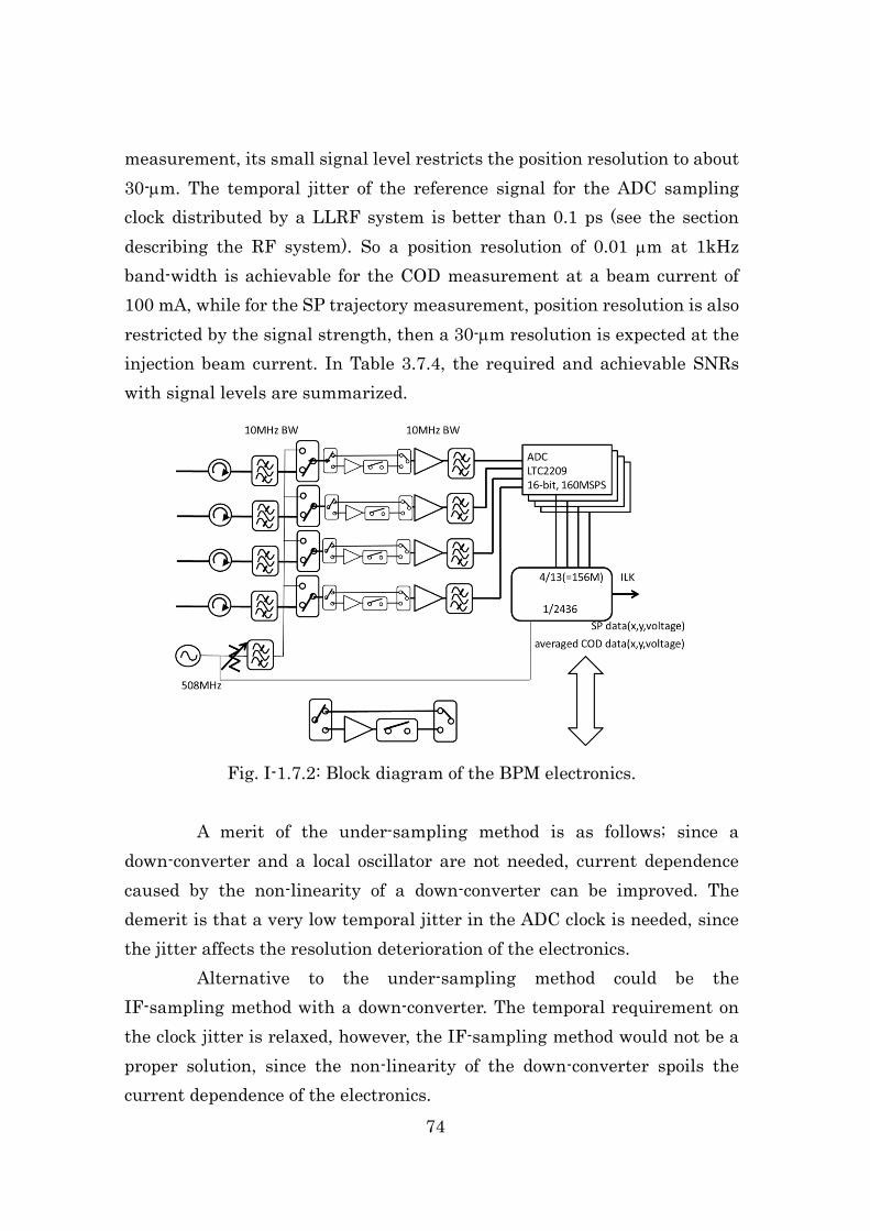
74
measurement, its small signal level restricts the position resolution to about 30-µm. The temporal jitter of the reference signal for the ADC sampling clock distributed by a LLRF system is better than 0.1 ps (see the section describing the RF system). So a position resolution of 0.01 µm at 1kHz band-width is achievable for the COD measurement at a beam current of 100 mA, while for the SP trajectory measurement, position resolution is also restricted by the signal strength, then a 30-µm resolution is expected at the injection beam current. In Table 3.7.4, the required and achievable SNRs with signal levels are summarized.
Fig. I-1.7.2: Block diagram of the BPM electronics.
A merit of the under-sampling method is as follows; since a down-converter and a local oscillator are not needed, current dependence caused by the non-linearity of a down-converter can be improved. The demerit is that a very low temporal jitter in the ADC clock is needed, since the jitter affects the resolution deterioration of the electronics.
Alternative to the under-sampling method could be the IF-sampling method with a down-converter. The temporal requirement on the clock jitter is relaxed, however, the IF-sampling method would not be a proper solution, since the non-linearity of the down-converter spoils the current dependence of the electronics.
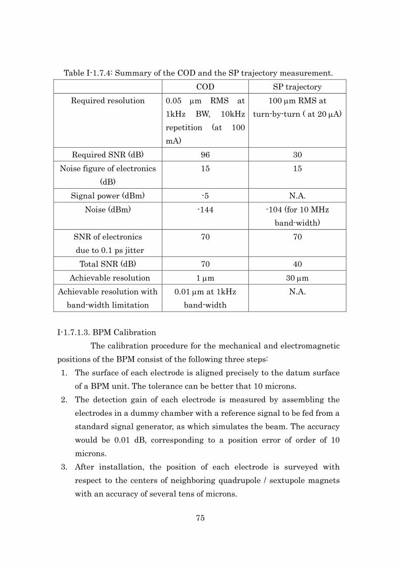
75
Table I-1.7.4: Summary of the COD and the SP trajectory measurement. COD SP trajectory
Required resolution 0.05 µm RMS at 1kHz BW, 10kHz repetition (at 100 mA)
100 µm RMS at turn-by-turn ( at 20 µA)
Required SNR (dB) 96 30 Noise figure of electronics
(dB) 15 15
Signal power (dBm) -5 N.A. Noise (dBm) -144 -104 (for 10 MHz
band-width) SNR of electronics due to 0.1 ps jitter
70 70
Total SNR (dB) 70 40 Achievable resolution 1 µm 30 µm
Achievable resolution with band-width limitation
0.01 µm at 1kHz band-width
N.A.
I-1.7.1.3. BPM Calibration The calibration procedure for the mechanical and electromagnetic
positions of the BPM consist of the following three steps: 1. The surface of each electrode is aligned precisely to the datum surface
of a BPM unit. The tolerance can be better that 10 microns. 2. The detection gain of each electrode is measured by assembling the
electrodes in a dummy chamber with a reference signal to be fed from a standard signal generator, as which simulates the beam. The accuracy would be 0.01 dB, corresponding to a position error of order of 10 microns.
3. After installation, the position of each electrode is surveyed with respect to the centers of neighboring quadrupole / sextupole magnets with an accuracy of several tens of microns.

76
By these procedures, we can expect the detection accuracy of the BPM is better than 100 µm. I-1.7.2. Beam Emittance Diagnostics at Storage Ring
For non-destructive diagnostics of the electron beam emittance, the transverse beam size should be measured by using synchrotron radiation emitted from a bending magnet. The BM3 or BM4 of the five bending magnets lattice of the SPring-8-II ring are possible candidates as light sources. The use of the BM3 or the BM4 allows us to install emittance measurement instrumentations without confliction among other accelerator equipment and the photon beamlines for user experiments. The smallest electron beam size in the bending magnets is 5 µm in RMS for the vertical plane at the source point of BM3 (see Table I-1.7.5). To observe the beam size, X-ray imaging by using a pinhole or a focusing element, such as a Fresnel zone plate [Takano2006], could be employed. The whole instrumentations for the beam emittance measurement is placed inside an accelerator tunnel, and, in this placement, the beam emittance is regularly monitored for machine tuning and user experiments.
Table I-1.7.5: Electron beam sizes in RMS at BM3 and ID source points. Source ( βx*εx )1/2(µm) ηx*σ/E(µm) σx (µm) σy (µm) Ec (keV) BM3 11.3 0.9 11.3 5.0 22.8 ID 26.5 0 26.5 6.2
I-1.7.3. Diagnostics of Injection Beam at Transport Line It is indispensable to diagnose the emittance, the transverse size,
the energy spread and the bunch length of an electron beam near to the injection point of the storage ring.
Since, as described in the section of injector, the emittance has to be less than 560 pm rad for a stable and highly-efficient beam injection, an emittance measurement resolution of less than one tenth of allowable emittance, i.e. 60 pm rad is required. The beam size should be diagnosed

77
with a resolution of less than 12 µm in RMS, which is one sixth of allowable beam size at the injection point. The energy spread and the bunch length of the injection beam should be less than 0.1 % and 7 ps from the designed energy spread and bunch length of the stored beam, respectively. Then the resolution of the diagnostics should sufficiently be less than them.
The emittance is evaluated by the Q-scan method using an OTR screen (A spatial resolution of less than 10 μm in RMS). This emittance evaluation is already working at a dispersion free section around the middle part of the beam transport line, XSBT, and its designed resolution is 60 pm rad. So the existing method is applicable to our emittance evaluation.
The beam size and the energy spread are also diagnosed by using an OTR screen. Suppose a dispersion function near the injection point of the beam transport line is 0.5 m, a spatial resolution of 10 µm is enough for a resolution of energy-spread measurement of within 0.01 %.
For a bunch length measurement system, a streak camera with an OTR radiator already realizes a temporal resolution of less than 300 fs in FWHM [Otake2013] and EO sampling works as a non-destructive and real-time temporal monitor using inorganic Pockels EO crystals, which could archive a temporal resolution of less than 200 fs in FWHM [Okayasu2013]. An enough resolution is obtained in both methods.
The beam trajectory near the injection point is measured by strip-line BPMs with a spatial resolution of 30 μm in RMS at a bunch charge of 80 pC. These measured positions are used for tuning of the beam injection.
I-1.7.4. Suppression of Beam Instabilities
In the transverse plane, resistive-wall impedance becomes a dominant source of electron beam instabilities because of a small-vertical vacuum chamber aperture of 16 mm and narrower gaps of 5 mm at a minimum in in-vacuum undulators. The growth rate of transverse instability due to the impedance is estimated to be 10 times faster than that of the present ring. The present transverse bunch-by-bunch feedback (BBF) system in the SPring-8 ring [Nakamura2005B] has enough capability to

78
suppress such strong instability. In the longitudinal direction, a longitudinal BBF system with a newly developed high-energy efficiency kicker [Nakamura2011, Masaki2013] is under development to cure suspected coupled-bunch-instability due to the HOMs of acceleration cavities. References
[Fujita2006] T. Fujita et al., EPAC2006, pp. 1130-1132, Edinburgh, Scotland (2006). [GEIP] http://ge-ip.com [Masaki2013] M. Masaki et al., IBIC2013, pp. 407-410, (2013). [Nakamura2005A] T. Nakamura, DIPAC2005, pp. 304-306, Lyon, France (2005). [Nakamura2005B]T. Nakamura, K. Kobayashi, ICALEPCS’05, PO02.022-2 (2005). [Nakamura2011] T. Nakamura, IPAC2011, pp. 493-495 (2011). [Okayasu2013] Y. Okayasu et al., Phys. Rev. ST Accel Beams 16, 052801 (2013). [Otake2013] Y. Otake et al., Phys. Rev. ST Accel. Beams 16, 042802 (2013). [Takano2006] S. Takano et al., Nucl. Instrum. Methods Phys. Res. A556, 357 (2006).

79
I-1.8 Injector I-1.8.1. Introduction
The use of SACLA as an injector of SPring-8-II has been considered to achieve good injection efficiency, low operation cost and minimum energy consumption. The SPring-8-II storage ring requires a low emittance injector due to its small dynamic aperture. Since the emittance of the injection beam is determined from its equilibrium state of the circulating electron beam in a synchrotron booster, it is hard to obtain a low emittance beam with the existing SPring-8 injector system composed of a linac and a FODO synchrotron. In addition, despite of a low injection frequency during top-up operation, it is necessary to maintain the injector system in a warmed-up condition, and it results in an increase of operation cost and energy consumption. On the other hand, the linac of SACLA is always running for its own user experiments independently from SPring-8-II. Therefore if the injection beam is distributed from SACLA, it will enable to save the energy consumption and operation cost for idling the accelerator.
The nominal beam energy of SPring-8-II is expected to be 6 GeV, whereas the beam energies used for the XFEL operation are around 5~8.5 GeV depending on the photon energy requested from the user experiment. In addition the electron bunch is highly compressed and its peak current reaches several kA, which is not necessary but even harmful for the injection beam due to the emittance degradation at a beam transport line. To achieve the SACLA XFEL operation and the beam injection to SPring-8-II in parallel, the control of the beam energy and the peak current is indispensable on a bunch-to-bunch basis.
I-1.8.2. Requirements on the Injection Beam
To avoid the beam loss, the injected beam should stay inside the dynamic aperture of the storage ring. The electron beam will be injected in a horizontal plane using an in-vacuum septum magnet at SPring-8-II, and a tentative normalized dynamic aperture 𝑥𝑑 of 2 mm1/2 is assumed as in Eq. (I-1.8.1).
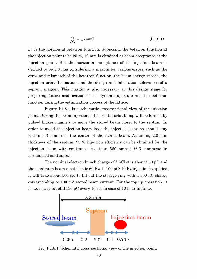
80
𝑥𝑑�𝛽𝑥
= ±2𝑚𝑚12 (I-1.8.1)
𝛽𝑥 is the horizontal betatron function. Supposing the betatron function at the injection point to be 25 m, 10 mm is obtained as beam acceptance at the injection point. But the horizontal acceptance of the injection beam is decided to be 3.3 mm considering a margin for various errors, such as the error and mismatch of the betatron function, the beam energy spread, the injection orbit fluctuation and the design and fabrication tolerances of a septum magnet. This margin is also necessary at this design stage for preparing future modification of the dynamic aperture and the betatron function during the optimization process of the lattice.
Figure I-1.8.1 is a schematic cross-sectional view of the injection point. During the beam injection, a horizontal orbit bump will be formed by pulsed kicker magnets to move the stored beam closer to the septum. In order to avoid the injection beam loss, the injected electrons should stay within 3.3 mm from the center of the stored beam. Assuming 2.0 mm thickness of the septum, 99 % injection efficiency can be obtained for the injection beam with emittance less than 560 pm-rad (6.6 mm-mrad in normalized emittance).
The nominal electron bunch charge of SACLA is about 200 pC and the maximum beam repetition is 60 Hz. If 100 pC- 10 Hz injection is applied, it will take about 500 sec to fill out the storage ring with a 500 nC charge corresponding to 100 mA stored-beam current. For the top-up operation, it is necessary to refill 130 pC every 10 sec in case of 10 hour lifetime.
Fig. I-1.8.1: Schematic cross-sectional view of the injection point.
0.265 0.2 2.0 0.1
3.3 mm
0.735
Septum
Stored beam Injection beam

81
I-1.8.3. Transport Line The beam transport line from SACLA to the exit of the existing
synchrotron booster had been already constructed together with the SACLA facility. The foremost concern about the beam transport is emittance degradation due to CSR effects. The lattice of this XSBT (XFEL to Synchrotron Beam Transport) line is based on DBA to mitigate emittance degradation. After XSBT, SSBT (Synchrotron to Storage ring Beam Transport) connects the exit of the synchrotron booster and the storage ring. SSBT has been used for the beam injection from the synchrotron booster to the current SPring-8 storage ring. The lattice of SSBT is based on FODO and not optimized for the transport of low emittance beams. The layout and lattice of XSBT and SSBT are shown in Figs. I-1.8.2 and I-1.8.3 respectively.
The emittance increase by CSR largely depends on the beam parameters, particularly the peak current and the energy spread. The kilo-ampere electron bunches used for the XFEL operation, whose bunch length is less than 10 fs (FWHM), will certainly not satisfy the required emittance of the beam injection. To prevent the emittance degradation at the transport line, the peak current should be reduced down to a few hundred amperes or less by lengthening the electron bunch.
Figure I-1.8.4 is an example of the emittance degradation through the beam transport line calculated with ELEGANT for the case of 8 GeV beams. In Fig. I-1.8.4 (a), 100 pm-rad initial emittance is assumed with 0.01% energy spread and a peak current of about 100 A without any energy chirp. Since there are both horizontal and vertical bending magnets in the transport line, the emittance is increased in both planes. Figure I-1.8.4 (b) is the case with energy chirp of 0.064 % over the full bunch length. The electron bunch is elongated by R56 of the first part of the transport line, and it results in the reduction of the peak current for the rest of the transport line. Thus the CSR effect and the emittance degradation are suppressed.
The beam transport through XSBT has been already tested. Further beam transport to the storage ring and the evaluation of the beam emittance are planned before the construction of SPring-8-II.
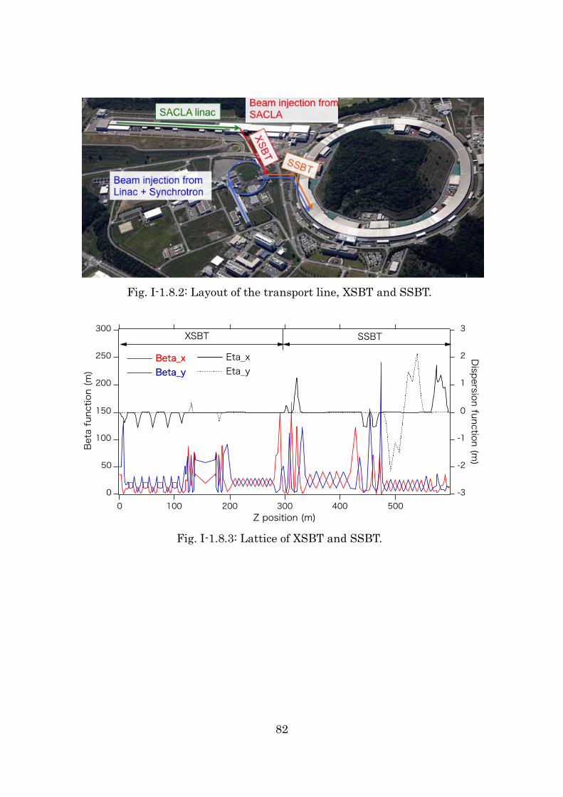
82
Fig. I-1.8.2: Layout of the transport line, XSBT and SSBT.
Fig. I-1.8.3: Lattice of XSBT and SSBT.
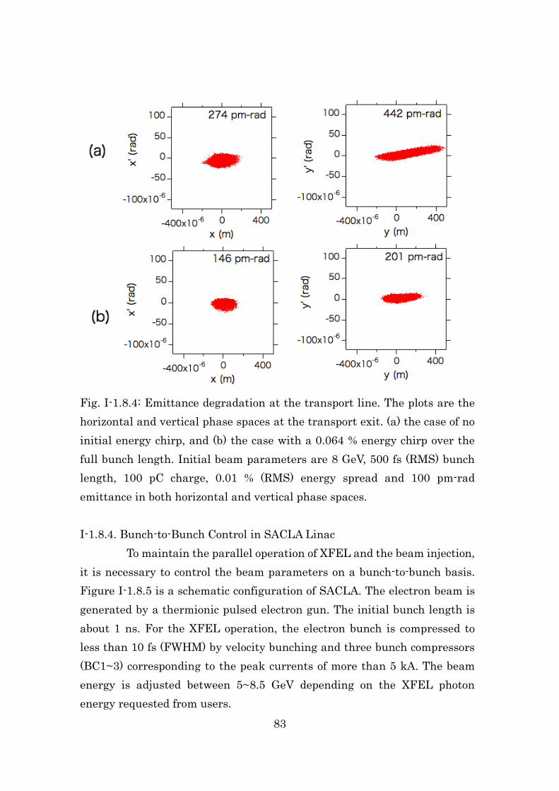
83
Fig. I-1.8.4: Emittance degradation at the transport line. The plots are the horizontal and vertical phase spaces at the transport exit. (a) the case of no initial energy chirp, and (b) the case with a 0.064 % energy chirp over the full bunch length. Initial beam parameters are 8 GeV, 500 fs (RMS) bunch length, 100 pC charge, 0.01 % (RMS) energy spread and 100 pm-rad emittance in both horizontal and vertical phase spaces. I-1.8.4. Bunch-to-Bunch Control in SACLA Linac
To maintain the parallel operation of XFEL and the beam injection, it is necessary to control the beam parameters on a bunch-to-bunch basis. Figure I-1.8.5 is a schematic configuration of SACLA. The electron beam is generated by a thermionic pulsed electron gun. The initial bunch length is about 1 ns. For the XFEL operation, the electron bunch is compressed to less than 10 fs (FWHM) by velocity bunching and three bunch compressors (BC1~3) corresponding to the peak currents of more than 5 kA. The beam energy is adjusted between 5~8.5 GeV depending on the XFEL photon energy requested from users.

84
Since it is necessary to keep the energy of the electron bunches at 6 GeV for the beam injection to SPring-8-II, the concept of multi-energy operation was proposed to share the bunches between XFEL and the beam injection [Hara2013]. In the multi-energy operation, the RF pulse repetitions of specific RF units are changed to control the beam energy from bunch to bunch.
The multi-energy operation has been successfully demonstrated at SACLA. Figure I-1.8.6 shows the energy of the electron bunches measured at a chicane located upstream of the BL3 undulators. In the demonstration, the repetition of the electron bunch was 10 Hz and 8 RF units were operated at 5 Hz. Since the beam energy gain of one RF unit is about 130 MeV, the beam energy is alternately changed from bunch to bunch between 8.0 GeV and 6.9 GeV. Once a kicker magnet is installed, the energy controlled electron bunches are distributed to the XFEL beamlines and the transport line.
For the beam injection to SPring-8-II, it is also necessary to elongate the bunch length, which is possible by controlling the RF phase to reduce the energy chirp at the bunch compressors. Since the electron beam should be injected on-demand timing from the storage ring during the top-up operation, the parameter of the RF units should be changed at any requested timing. In order to achieve the bunch-to-bunch control of the beam energy, the bunch length and the energy chirp, a new timing and low-level RF systems are under study.
At SACLA, a bunch-to-bunch beam distribution system using a kicker magnet and a DC twin-septum magnet is planned to be installed in the winter shutdown of 2014 for the multi-beamline XFEL operation. The electron bunch distribution with controlled energy and length at arbitrary timing will be further investigated and examined using the electron beam. Reference [Hara2013] T. Hara et al., Phys. Rev. ST Accel. Beams 16 (2013) 080701.

85
Fig. I-1.8.5: Schematic configuration of the SACLA accelerator.
Fig. I-1.8.6: The multi-energy operation demonstrated at SACLA. In this example, the electron bunch repetition is 10 Hz and the beam energy is alternately changed between 8.0 GeV and 6.9 GeV.
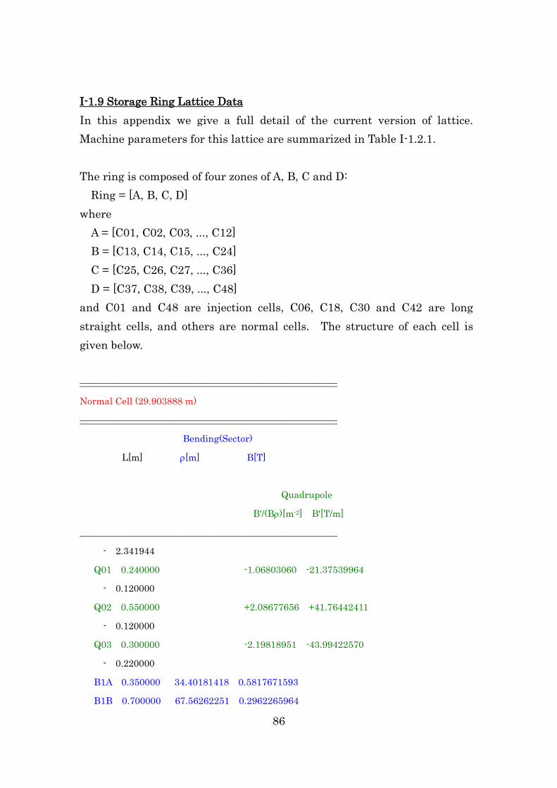
86
I-1.9 Storage Ring Lattice Data In this appendix we give a full detail of the current version of lattice. Machine parameters for this lattice are summarized in Table I-1.2.1. The ring is composed of four zones of A, B, C and D: Ring = [A, B, C, D] where A = [C01, C02, C03, ..., C12] B = [C13, C14, C15, ..., C24] C = [C25, C26, C27, ..., C36] D = [C37, C38, C39, ..., C48] and C01 and C48 are injection cells, C06, C18, C30 and C42 are long straight cells, and others are normal cells. The structure of each cell is given below. _______________________________________________________
Normal Cell (29.903888 m)
_______________________________________________________
Bending(Sector)
L[m] ρ[m] B[T]
Quadrupole
B'/(Bρ)[m-2] B'[T/m]
_______________________________________________________
- 2.341944
Q01 0.240000 -1.06803060 -21.37539964
- 0.120000
Q02 0.550000 +2.08677656 +41.76442411
- 0.120000
Q03 0.300000 -2.19818951 -43.99422570
- 0.220000
B1A 0.350000 34.40181418 0.5817671593
B1B 0.700000 67.56262251 0.2962265964

87
B1C 0.700000 120.89241670 0.1655508779
- 0.120000
Q04 0.200000 -1.93398472 -38.70647180
- 0.120000
S1 0.300000
- 0.420000
O1 0.160000
- 0.120000
S2 0.180000
- 0.120000
Q05 0.300000 +2.76586723 +55.35564000
- 0.120000
S3 0.180000
- 0.420000
O2 0.160000
- 0.120000
S4 0.300000
- 0.120000
Q06 0.200000 -2.27291040 -45.48967806
- 0.120000
B2D 0.700000 90.73380781 0.2205776016
B2E 0.700000 50.70806566 0.3946876192
B2F 0.350000 25.81971064 0.7751382651
- 0.120000
Q07 0.700000 +2.13318029 +42.69314120
- 0.270000
Q08 0.700000 -2.22567622 -44.54434047
- 0.270000
Q09 0.650000 +2.40641274 +48.16157330
- 0.270000
Q10 0.300000 -0.71315042 -14.27288248
- 0.290000
B3G 0.420000 21.00000000 0.9530402720
88
- 0.290000
Q10 0.300000 -0.71315042 -14.27288248
- 0.270000
Q09 0.650000 +2.40641274 +48.16157330
- 0.270000
Q08 0.700000 -2.22567622 -44.54434047
- 0.270000
Q07 0.700000 +2.13318029 +42.69314120
- 0.120000
B4F 0.350000 25.81971064 0.7751382651
B4E 0.700000 50.70806566 0.3946876192
B4D 0.700000 90.73380781 0.2205776016
- 0.120000
Q06 0.200000 -2.27291040 -45.48967806
- 0.120000
S5 0.300000
- 0.700000
S6 0.180000
- 0.120000
Q05 0.300000 +2.76586723 +55.35564000
- 0.120000
S7 0.180000
- 0.420000
O3 0.160000
- 0.120000
S8 0.300000
- 0.120000
Q04 0.200000 -1.93398472 -38.70647180
- 0.120000
B5C 0.700000 120.89241670 0.1655508779
B5B 0.700000 67.56262251 0.2962265964
B5A 0.350000 34.40181418 0.5817671593
- 0.220000
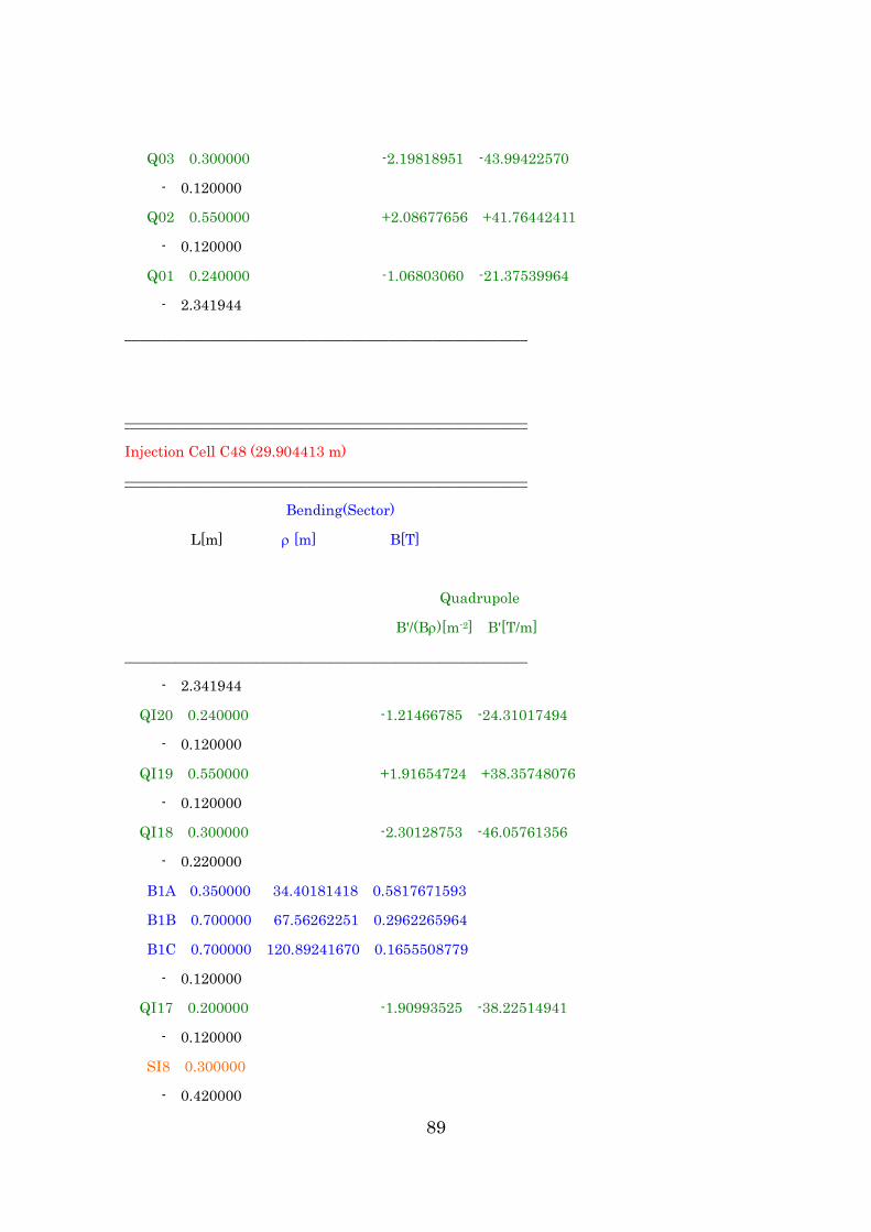
89
Q03 0.300000 -2.19818951 -43.99422570
- 0.120000
Q02 0.550000 +2.08677656 +41.76442411
- 0.120000
Q01 0.240000 -1.06803060 -21.37539964
- 2.341944
_______________________________________________________
_______________________________________________________
Injection Cell C48 (29.904413 m)
_______________________________________________________
Bending(Sector)
L[m] ρ [m] B[T]
Quadrupole
B'/(Bρ)[m-2] B'[T/m]
_______________________________________________________
- 2.341944
QI20 0.240000 -1.21466785 -24.31017494
- 0.120000
QI19 0.550000 +1.91654724 +38.35748076
- 0.120000
QI18 0.300000 -2.30128753 -46.05761356
- 0.220000
B1A 0.350000 34.40181418 0.5817671593
B1B 0.700000 67.56262251 0.2962265964
B1C 0.700000 120.89241670 0.1655508779
- 0.120000
QI17 0.200000 -1.90993525 -38.22514941
- 0.120000
SI8 0.300000
- 0.420000
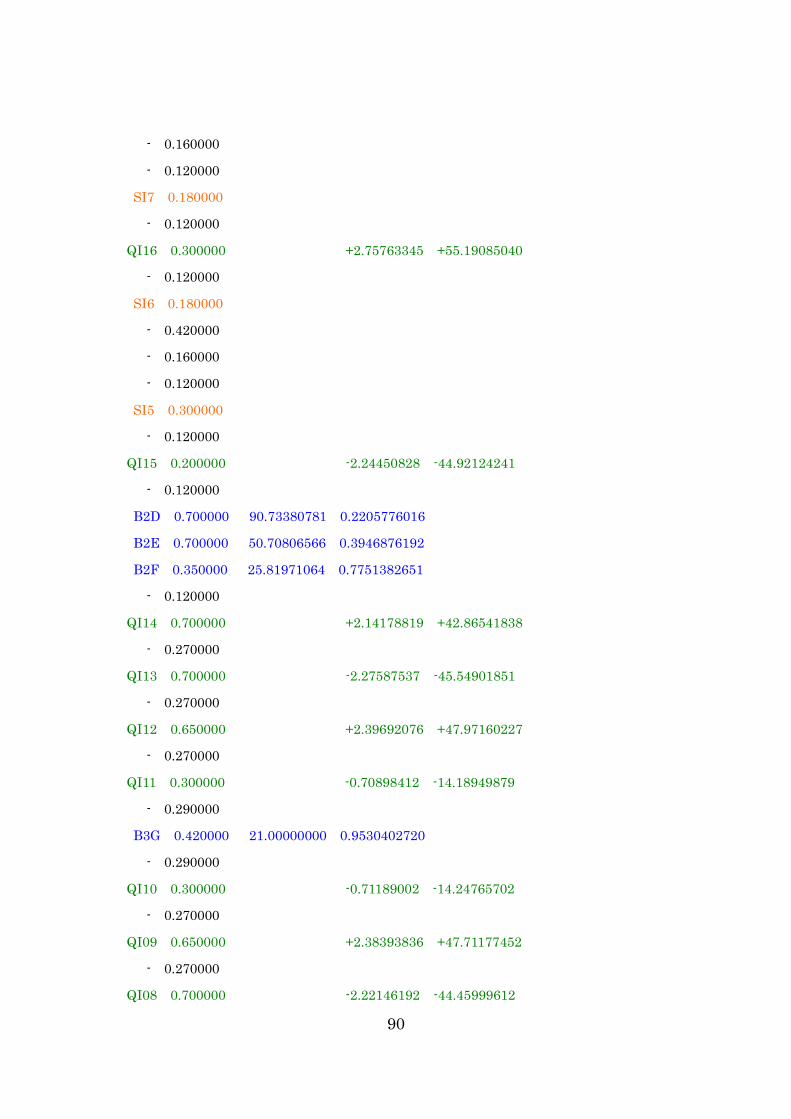
90
- 0.160000
- 0.120000
SI7 0.180000
- 0.120000
QI16 0.300000 +2.75763345 +55.19085040
- 0.120000
SI6 0.180000
- 0.420000
- 0.160000
- 0.120000
SI5 0.300000
- 0.120000
QI15 0.200000 -2.24450828 -44.92124241
- 0.120000
B2D 0.700000 90.73380781 0.2205776016
B2E 0.700000 50.70806566 0.3946876192
B2F 0.350000 25.81971064 0.7751382651
- 0.120000
QI14 0.700000 +2.14178819 +42.86541838
- 0.270000
QI13 0.700000 -2.27587537 -45.54901851
- 0.270000
QI12 0.650000 +2.39692076 +47.97160227
- 0.270000
QI11 0.300000 -0.70898412 -14.18949879
- 0.290000
B3G 0.420000 21.00000000 0.9530402720
- 0.290000
QI10 0.300000 -0.71189002 -14.24765702
- 0.270000
QI09 0.650000 +2.38393836 +47.71177452
- 0.270000
QI08 0.700000 -2.22146192 -44.45999612
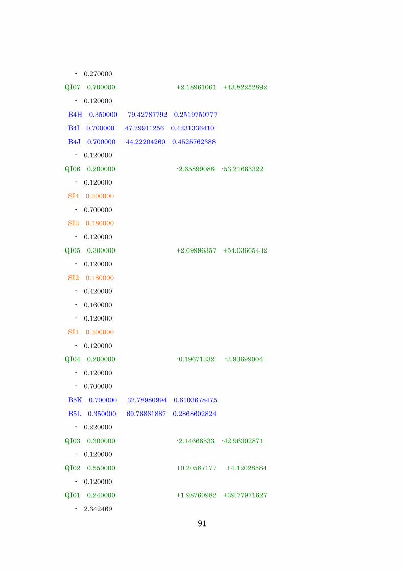
91
- 0.270000
QI07 0.700000 +2.18961061 +43.82252892
- 0.120000
B4H 0.350000 79.42787792 0.2519750777
B4I 0.700000 47.29911256 0.4231336410
B4J 0.700000 44.22204260 0.4525762388
- 0.120000
QI06 0.200000 -2.65899088 -53.21663322
- 0.120000
SI4 0.300000
- 0.700000
SI3 0.180000
- 0.120000
QI05 0.300000 +2.69996357 +54.03665432
- 0.120000
SI2 0.180000
- 0.420000
- 0.160000
- 0.120000
SI1 0.300000
- 0.120000
QI04 0.200000 -0.19671332 -3.93699004
- 0.120000
- 0.700000
B5K 0.700000 32.78980994 0.6103678475
B5L 0.350000 69.76861887 0.2868602824
- 0.220000
QI03 0.300000 -2.14666533 -42.96302871
- 0.120000
QI02 0.550000 +0.20587177 +4.12028584
- 0.120000
QI01 0.240000 +1.98760982 +39.77971627
- 2.342469
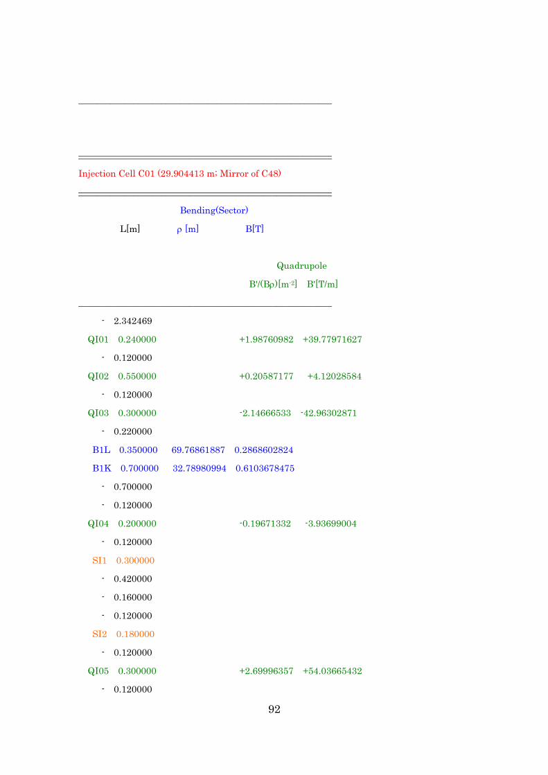
92
_______________________________________________________
_______________________________________________________
Injection Cell C01 (29.904413 m; Mirror of C48)
_______________________________________________________
Bending(Sector)
L[m] ρ [m] B[T]
Quadrupole
B'/(Bρ)[m-2] B'[T/m]
_______________________________________________________
- 2.342469
QI01 0.240000 +1.98760982 +39.77971627
- 0.120000
QI02 0.550000 +0.20587177 +4.12028584
- 0.120000
QI03 0.300000 -2.14666533 -42.96302871
- 0.220000
B1L 0.350000 69.76861887 0.2868602824
B1K 0.700000 32.78980994 0.6103678475
- 0.700000
- 0.120000
QI04 0.200000 -0.19671332 -3.93699004
- 0.120000
SI1 0.300000
- 0.420000
- 0.160000
- 0.120000
SI2 0.180000
- 0.120000
QI05 0.300000 +2.69996357 +54.03665432
- 0.120000
93
SI3 0.180000
- 0.420000
- 0.160000
- 0.120000
SI4 0.300000
- 0.120000
QI06 0.200000 -2.65899088 -53.21663322
- 0.120000
B2J 0.700000 44.22204260 0.4525762388
B2I 0.700000 47.29911256 0.4231336410
B2H 0.350000 79.42787792 0.2519750777
- 0.120000
QI07 0.700000 +2.18961061 +43.82252892
- 0.270000
QI08 0.700000 -2.22146192 -44.45999612
- 0.270000
QI09 0.650000 +2.38393836 +47.71177452
- 0.270000
QI10 0.300000 -0.71189002 -14.24765702
- 0.290000
B3G 0.420000 21.00000000 0.9530402720
- 0.290000
QI11 0.300000 -0.70898412 -14.18949879
- 0.270000
QI12 0.650000 +2.39692076 +47.97160227
- 0.270000
QI13 0.700000 -2.27587537 -45.54901851
- 0.270000
QI14 0.700000 +2.14178819 +42.86541838
- 0.120000
B4F 0.350000 25.81971064 0.7751382651
B4E 0.700000 50.70806566 0.3946876192
B4D 0.700000 90.73380781 0.2205776016

94
- 0.120000
QI15 0.200000 -2.24450828 -44.92124241
- 0.120000
SI5 0.300000
- 0.700000
SI6 0.180000
- 0.120000
QI16 0.300000 +2.75763345 +55.19085040
- 0.120000
SI7 0.180000
- 0.420000
- 0.160000
- 0.120000
SI8 0.300000
- 0.120000
QI17 0.200000 -1.90993525 -38.22514941
- 0.120000
B5C 0.700000 120.89241670 0.1655508779
B5B 0.700000 67.56262251 0.2962265964
B5A 0.350000 34.40181418 0.5817671593
- 0.220000
QI18 0.300000 -2.30128753 -46.05761356
- 0.120000
QI19 0.550000 +1.91654724 +38.35748076
- 0.120000
QI20 0.240000 -1.21466785 -24.31017494
- 2.341944
_______________________________________________________
_______________________________________________________
Long Straight Cell C06, C18, C30, C42 (29.915600 m)
_______________________________________________________

95
Bending(Sector)
L[m] ρ [m] B[T]
Quadrupole
B'/(Bρ)[m-2] B'[T/m]
_______________________________________________________
- 2.437800
QL1 0.500000 +0.98004213 +19.61441198
- 0.500000
QL2 0.500000 -1.44051710 -28.83028698
- 0.400000
QL3 0.300000 -0.07608812 -1.52281589
- 0.400000
QL4 0.500000 +0.68442003 +13.69787688
- 1.941100
- 1.941100
QL4 0.500000 +0.68442003 +13.69787688
- 0.400000
QL3 0.300000 -0.07608812 -1.52281589
- 0.400000
QL2 0.500000 -1.44051710 -28.83028698
- 0.500000
QL1 0.500000 +0.98004213 +19.61441198
- 2.437800
- 2.437800
QL1 0.500000 +0.98004213 +19.61441198
- 0.500000
QL2 0.500000 -1.44051710 -28.83028698
- 0.400000
QL3 0.300000 -0.07608812 -1.52281589
- 0.400000
QL4 0.500000 +0.68442003 +13.69787688
- 1.941100

96
- 1.941100
QL4 0.500000 +0.68442003 +13.69787688
- 0.400000
QL3 0.300000 -0.07608812 -1.52281589
- 0.400000
QL2 0.500000 -1.44051710 -28.83028698
- 0.500000
QL1 0.500000 +0.98004213 +19.61441198
- 2.437800
_______________________________________________________
_______________________________________________________
Sextupole (typical)
L[m] B"L/(Bρ)/2[m-2] B"/(Bρ)[m-3] B"[Tm-2]
_______________________________________________________
S1 0.300000 -19.60 -130.66667 -2615.1425
S2 0.180000 +9.332024 +103.68916 +2075.2188
S3 0.180000 +7.28 +80.88889 +1618.8977
S4 0.300000 -10.83 -72.20000 -1444.9997
S5 0.300000 ( = S4 )
S6 0.180000 ( = S3 )
S7 0.180000 ( = S2 )
S8 0.300000 ( = S1 )
SI1 0.300000 -19.60 -130.66667 -2615.1425
SI2 0.180000 +9.332024 +103.68916 +2075.2188
SI3 0.180000 +7.21 +80.11111 +1603.3314
SI4 0.300000 -10.70 -71.333333 -1427.6543
SI5 0.300000 ( = SI4 )
SI6 0.180000 ( = SI3 )
SI7 0.180000 ( = SI2 )

97
SI8 0.300000 ( = SI1 )
_______________________________________________________
_______________________________________________________
Octupole (typical)
L[m] B(3)L/(Bρ)/6[m-3] B(3)/(Bρ)[m-4] B(3)[Tm-3]
_______________________________________________________
O1 0.160000 -43.3543 -1625.79 -32538.2
O2 0.160000 -57.4151 -2153.07 -43091.1
O3 0.160000 -58.2721 -2185.20 -43734.2
_______________________________________________________
98
PART-I I-2 Light Sources
I-2.1. Basic Policy of ID Specification I-2.2. Hard X-ray Beamline I-2.3. Soft X-ray Beamline I-2.4. Expected Light Source Performances I-2.5. Facilitating the Mass Production and Installation of IDs I-2.6. Summary
99
In this chapter, specifications of insertion devices (IDs) to be installed in the upgraded storage ring are described and light source performances available in SPring-8-II are discussed. Firstly, the basic policy of how to define the specifications of IDs is described from the practical point of view. Secondly, detailed specifications of IDs in several typical beamlines are presented together with expected light source performances, which are computed with a more rigorous method than the traditional one based on a Gaussian approximation. Finally, a couple of technical issues are addressed toward mass production of IDs, which are crucial for the schedule and budget of SPring-8-II. Note that all the computations shown in the following sections are carried out with the SR calculation code SPECTRA [Tanaka2001]. I-2.1. Basic Policy of ID Specification
The insertion device (ID), in which the high-quality electron beam generates synchrotron radiation (SR), is one of the key components in SPring-8-II. Although there exist a lot of IDs currently installed in the existing storage ring of SPring-8, most of them cannot be used as is in SPring-8-II because of two reasons.
Firstly, the straight sections for installation of IDs in the upgraded storage ring will be shortened to around 4.7 m, nearly 1 m shorter than the current value in SPring-8, and thus the IDs should be shorter as well. This is to accommodate a lot of magnets required for the 5BA (5-bend achromat) lattice instead of the current DBA (double-bend achromat) lattice. Secondly, the electron energy is reduced from 8 GeV to 6 GeV to improve the emittance of the electron beam. In order to make sure that the tunable range of SR is comparable to that in SPring-8, the magnetic design of IDs should be revised.
In order to meet the requirements above, we have to at least refurbish the existing IDs to fit the new straight sections, or more preferably, replace them with new ones. In designing the new IDs, we have to keep in mind that the emittance of the electron beam will be reduced by a factor of nearly 20, in order to take full advantage of the performance of the

100
upgraded storage ring.
I-2.1.1. Consideration of Light Source Performance In order to consider the specifications of IDs, we need to answer a
fundamental question: what kind of quality is important as the SR light source?
The performance of a light source is defined by a lot of parameters. Among them, we have three important characteristics of radiation in SR beamlines: brilliance (or brightness), total flux, and transverse coherence, which are directly related to the number of photons to be actually delivered to the sample.
In order to discuss the practical performance of a specific SR beamline, we need to consider another important property of radiation, i.e., the radiation power, which denotes the photon intensity obtained by integrating the photon flux over the entire energy range. In most experiments using monochromatic photon beams, only the photons contained in a narrow bandwidth (typically of the order of 10-3~10-4) around the target photon energy are extracted by the monochromator and guided to the sample. All the other photons outside the monochromator bandwidth are usually absorbed by front-end components and optical elements in the beamline and then turn to heat sources. If the cooling capability of a particular component is not sufficient, it can be significantly damaged or at least deformed.
The heat load problem explained above is especially serious for the optical elements such as focusing mirrors and monochromators, because the deformation of these devices results in a fluctuation of the photon beam position and size at the sample, and a variation of the energy resolution. As a result, the effective brilliance and flux can be significantly reduced. In this sense, specifications of IDs should be defined not only to increase the brilliance and flux but also to reduce the radiation power or heat load, especially on the optical elements.

101
I-2.1.2. Undulators or Wigglers? It is well known that IDs can be classified into two types, i.e.,
undulators and wigglers. Although the magnetic structures of these two devices are identical in the point that they both generate periodic magnetic fields with the period of 𝜆𝑢 and peak field of 𝐵 , the radiation characteristics are completely different from each other. Namely, undulator radiation (UR) is coherent, while wiggler radiation is incoherent (WR). As a result, the brilliance of the former is always much higher than that of the latter, and thus we usually adopt an undulator for most applications, as long as it is available as a light source. To be specific, we need to consider the energy region ℏω𝑢 in which the undulator effectively works. Roughly speaking, it scales as
ω𝑢 ∝ 𝐸2/𝜆𝑢, (I-2.1.1)
where 𝐸 is the electron energy. Apart from technical issues such as machining and assembling of tiny magnets, the magnet period 𝜆𝑢 has a lower limit determined by a practical application. This is related to the peak field 𝐵 available in an ID, which scales as
𝐵 ∝ exp (−𝜋𝑔/𝜆𝑢), (I-2.1.2)
where 𝑔 is the magnet gap. The above formula means that the peak field exponentially decays as the ratio 𝑔/𝜆𝑢 , and thus 𝜆𝑢 cannot be much shorter than the minimum gap available in the storage ring, or more specifically, that at the straight section where the ID is installed. The lower limit of 𝜆𝑢 in turn determines the upper limit of the photon energy reached by an undulator. If the target photon energy is too high to be cover by any undulators, we have to turn to a wiggler, whose effective energy region ℏω𝑤 scales as
ω𝑤 ∝ 𝐸2𝐵. (I-2.1.3)
Note that the peak field 𝐵 should be strong enough to reach the target energy region, which usually imposes a longer period at the expense of the number of periods.
In SPring-8, all IDs are of undulator type except one exception in BL08W, thanks to the high electron energy of 8 GeV. This in turn means
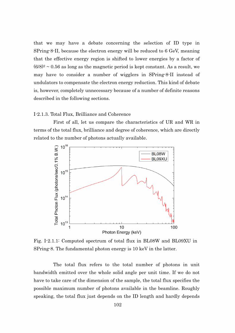
102
that we may have a debate concerning the selection of ID type in SPring-8-II, because the electron energy will be reduced to 6 GeV, meaning that the effective energy region is shifted to lower energies by a factor of (6/8)2 ~ 0.56 as long as the magnetic period is kept constant. As a result, we may have to consider a number of wigglers in SPring-8-II instead of undulators to compensate the electron energy reduction. This kind of debate is, however, completely unnecessary because of a number of definite reasons described in the following sections. I-2.1.3. Total Flux, Brilliance and Coherence
First of all, let us compare the characteristics of UR and WR in terms of the total flux, brilliance and degree of coherence, which are directly related to the number of photons actually available.
Fig. I-2.1.1: Computed spectrum of total flux in BL08W and BL09XU in SPring-8. The fundamental photon energy is 10 keV in the latter.
The total flux refers to the total number of photons in unit
bandwidth emitted over the whole solid angle per unit time. If we do not have to take care of the dimension of the sample, the total flux specifies the possible maximum number of photons available in the beamline. Roughly speaking, the total flux just depends on the ID length and hardly depends

103
on the ID type, as long as the parameters such as the magnetic period and strength are appropriately set. For example, Fig. I-2.1.1 shows the computed spectrum of total flux in BL08W (wiggler) and BL09XU (undulator) in SPring-8. Note that the fundamental photon energy in BL09XU has been assumed to be 10 keV, at which the total flux is found to be of the order of 1015 in both beamlines.
The above discussion on the total flux seems contradictory to the well-known fact that the brilliance of UR is much higher than that of WR. This is associated with the coherent properties of radiation as described below.
It has been mentioned in section I-2.1.2 that UR is coherent. To be more specific, the transverse coherence of radiation emitted from a single electron moving in an undulator is nearly perfect. As a result, most photons in UR are localized and contained in the coherent volume in the phase space. In other words, the optical emittance of UR is comparable to that of the diffraction-limited light.
On the other hand, photons in WR, which is an incoherent light source, are distributed widely throughout the phase space. In other words, the optical emittance is much larger than that of the diffraction-limited light, and that of UR.
Now let us recall the fact that the brilliance is given by the maximum photon density in the 4-dimensional phase space and is thus roughly given as the total flux divided by the optical emittance. It is easy to understand that the brilliance of WR is much lower than that of UR, typically by a few orders of magnitude. In practice, we have to consider the effects due to the finite emittance and energy spread of the electron beam, which always deteriorates the coherent properties of UR and degrades the brilliance. In other words, the low emittance electron beam is much more effective for UR than for WR.
I-2.1.4. Heat Load Reduction
Secondly, let us consider the selection of ID type in terms of how to reduce the heat load on optical elements. For this purpose, we need to
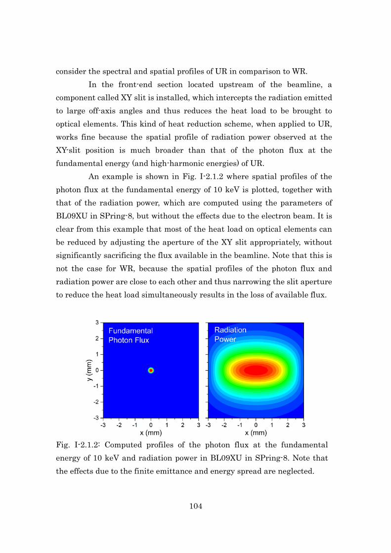
104
consider the spectral and spatial profiles of UR in comparison to WR. In the front-end section located upstream of the beamline, a
component called XY slit is installed, which intercepts the radiation emitted to large off-axis angles and thus reduces the heat load to be brought to optical elements. This kind of heat reduction scheme, when applied to UR, works fine because the spatial profile of radiation power observed at the XY-slit position is much broader than that of the photon flux at the fundamental energy (and high-harmonic energies) of UR.
An example is shown in Fig. I-2.1.2 where spatial profiles of the photon flux at the fundamental energy of 10 keV is plotted, together with that of the radiation power, which are computed using the parameters of BL09XU in SPring-8, but without the effects due to the electron beam. It is clear from this example that most of the heat load on optical elements can be reduced by adjusting the aperture of the XY slit appropriately, without significantly sacrificing the flux available in the beamline. Note that this is not the case for WR, because the spatial profiles of the photon flux and radiation power are close to each other and thus narrowing the slit aperture to reduce the heat load simultaneously results in the loss of available flux.
Fig. I-2.1.2: Computed profiles of the photon flux at the fundamental energy of 10 keV and radiation power in BL09XU in SPring-8. Note that the effects due to the finite emittance and energy spread are neglected.

105
It is worth noting here that the validity of the above discussions largely depends on the electron beam emittance. If it is much larger than the emittance of diffraction-limited light at the target photon energy, the heat load reduction using the XY slit is not so advantageous because the flux profile is broadened by the convolution with the electron beam distribution. This in turn means that the low emittance electron beam is directly linked to the effective reduction of the heat load of UR.
Another important point to be mentioned is the difference in spectral property between UR and WR. The spectrum of WR is essentially broadband as in the case of BM radiation and does not largely depend on the electron beam quality. On the other hand, the spectrum of UR is quasi monochromatic, if the aperture of the XY slit is adjusted appropriately. Its bandwidth gets narrower for smaller emittance and energy spread of the electron beam.
Summarizing the above discussions, undulators are superior to wigglers in terms of not only the brilliance but also the heat load reduction. I-2.1.5. Shortest Magnetic Period Available in SPring-8-II
As explained in the former two sections, undulators are much more advantageous than wigglers especially in the low-emittance storage ring to be achieved in SPring-8-II. Now we have to consider how to compensate the electron energy reduction, or more specifically, how we can shorten the magnetic period of undulators.
In fact, the shortest magnetic period to be available in SPring-8-II can be much shorter than that in SPring-8, because the possible minimum gap is expected to be narrower because of two factors. One is the shorter ID length and the other is the shorter vertical betatron function at the center of the straight section. As a result, the betatron function at the end of an ID, which determined the available minimum gap, becomes shorter than the current value by nearly 40 %. Based on the operational experience with the existing storage ring, the minimum gap available in SPring-8-II has been determined to be 5 mm, which is much narrower than the current minimum gap of 7 mm and thus the magnetic period of undulator can be shorter

106
accordingly. It should be also mentioned that the shorter period results in a larger number of periods, and thus higher flux and brilliance as well.
The bottom line is that undulators are supposed to be the main IDs in SPring-8-II and the choice of wigglers should not be made unless the users request special optical properties that cannot be provided by undulators, such as a white spectrum or broad spatial profile.
In the following sections, specifications of undulators to be installed in several typical beamlines are presented together with the computation results of expected light source performances. I-2.2. Hard X-ray Beamline
Firstly, specifications of undulators for hard x-ray beamlines (HXBLs) are discussed. In SPring-8, in-vacuum undulators (IVUs) [Hara1998a] have been aggressively adopted in pursuit of shortening the magnetic period. We will keep this concept as well in SPring-8-II, or rather, will explore utilization of more advanced form of IVUs, i.e., the cryogenic permanent magnet undulators (CPMUs) [Hara2004], toward further shortening of the magnetic period. I-2.2.1. Selection of Permanent Magnet Material
Before discussing the specifications for HXBLs, we need to consider the permanent magnet (PM) material for undulators in SPring-8-II.
Concerning the selection of PMs for IVUs, we have to keep in mind that they will undergo high-temperature bake-out processes and will be continuously placed in a high dose environment inside the storage ring. These two factors can lead to significant demagnetization of PMs and degradation of undulator performance. In order to avoid such a problem, we have to make sure that the coercivity of PM material, which is related to resistivity against demagnetization, should be high enough. In SPring-8, we have a criterion that the coercivity of PMs for IVUs should be at least higher than 2000 kA/m. In addition, all the PMs are annealed at a temperature slightly higher than that at the bake-out process in advance of assembly.
107
This thermal process improves the resistivity against demagnetization due to two sources, i.e., high temperature at the bake-out process and radiation damage during operation [Bizen2003]. Although we have never encountered a serious problem due to radiation damage of PMs in IVUs in SPring-8, we have to carefully examine if the above criteria and schemes are really sufficient, based on the operational experience of IVUs in SPring-8.
One good example may be the long-term change of integrated field observed specifically in the IVU for BL10XU, which might be probably due to radiation-induced demagnetization [Tanaka2011a]. After some inspection, it was found that the IVU was misaligned in the vertical direction, leading to reduction of the effective gap. Namely, the IVU had been operated at the effective minimum gap of 6.5 mm for many years, which was the narrowest aperture in the ring. As a result, a large fraction of electron loss took place at the entrance and damaged the PMs. Note that the demagnetization was localized at the entrance, and the light source performances such as the spectral and spatial profiles were not deteriorated at all.
The above experience suggests that the selection and thermal treatment of PMs are valid, if the condition in SPring-8-II is similar to that in SPring-8. The impact of the narrower minimum gap supposed in SPring-8-II may not be large, because it has been determined according to the shorter ID length and vertical betatron function. If we keep the criterion on the coercivity (> 2000 kA/m), we can make use of PMs with the average remanence of 1.25 T, which is about 10 % higher than that of PMs for IVUs in SPring-8. This improvement comes from the year-by-year advancement of PM technology such as the Dysprosium-diffusion technique.
As for the selection of PMs for CPMUs, we do not have to take care of the radiation damage too much, because the coercivity is drastically improved by cooling down the PMs to a cryogenic temperature. The only condition that the PM material should satisfy is that the PMs are not demagnetized during assembly at room temperature, when a strong demagnetizing field can be applied to the PMs. With this in mind, we can make use of PMs with the average remanence of 1.5 T at a cryogenic temperature.

108
Note that both of the above values, 1.25 T for IVUs and 1.5 T for CPMUs, are rather conservative, and PM materials with higher remanence may be available, according to the advancement of PM technology. I-2.2.2. Magnetic Configuration and Period
Having specified the remanence of PM material, let us discuss the possible magnetic period of IVUs for SPring-8-II. There are two familiar PM configurations to generate the sinusoidal field distribution necessary for undulators: Halbach and hybrid. For short-period undulators, the latter configuration is more advantageous in terms of the achievable field strength and feasibility of field correction, which is thus adopted in IVUs for HXBLs.
Fig. I-2.2.1: (a) Maximum K value at the minimum gap and (b) energy range available by the fundamental radiation, computed as a function of the period length.
109
In order to select the magnetic period, we have to consider the tunable range of UR under the boundary conditions such as the minimum gap and remanence of PM material. In other words, we need to estimate the maximum field strength, or more specifically, the maximum K value generated at the minimum gap, which has been carried out by numerical computation with the code RADIA [Chubar1998], with an assumption that the design of individual PM units are conventional, i.e., no special technique is applied to enhance the field strength such as additional PMs or inclined magnetization.
The computation results are shown in Fig. I-2.2.1 (a), where the maximum K values 𝐾𝑚𝑎𝑥 are plotted as a function of the magnetic period for two different values of remanence (Br). The lowest and highest fundamental photon energies of UR, ℏ𝜔1𝐿 and ℏ𝜔1𝐻 , are calculated by substituting 𝐾 = 𝐾𝑚𝑎𝑥 and 𝐾 = 0 into the well-known formula of the fundamental photon energy of UR,
𝜔1 = 4𝜋𝛾2𝑐𝜆𝑢(1+𝐾2/2)
, (I-2.2.1)
where 𝛾 = 1.174 × 10⁴ is the Lorentz factor of the 6-GeV electron beam. The results are shown in Fig. I-2.2.1 (b) for the two values of Br. For example, the selection of IVU (Br = 1.25 T) with 𝜆𝑢 = 18 mm results in 𝐾𝑚𝑎𝑥 = 1.66, and the fundamental radiation ranges from 8 keV to 19 keV.
Based on these results, the selection of the magnetic period is discussed for several typical HXBLs in the following sections. I-2.2.3. Standard Undulator for Wide Tunability
Firstly, we consider the magnetic period of “standard undulator”, which is supposed to be the main light sources in SPring-8-II. The most important specification of the standard undulator is that it should be widely tunable to be adapted to a variety of SR applications. This means that the tuning curves of respective harmonics of UR connect continuously with each other without no energy gap. Here, the tuning curve of a specific harmonic denotes the relation between the available photon flux or brilliance and the harmonic photon energy.

110
One criterion to realize the above condition is, roughly speaking, that the maximum K value is larger than 2.3 as indicated by the dashed line in Fig. I-2.2.1 (a), so that the tuning curves of the fundamental and 3rd harmonic are connected smoothly. In addition, the tunable range should go below 5 keV, which is another criterion for the standard HXBL adopted in SPring-8. We find that the magnetic period of the standard undulator should be longer than 22 mm for IVUs and 20 mm for CPMUs, in order to satisfy the above conditions.
Now let us discuss the utilization of CPMUs in SPring-8-II. We have two points to be concerned about in adopting the CPMUs as standard undulators: initial and running cost of the device, and feasibility of mass production.
We first consider the cost of the device. In order to cool down the PMs to a cryogenic temperature, we have two possible solutions. One is to utilize refrigerators, and the other is to circulate liquid nitrogen (LN2). Note that the LN2 circulation system will be also required for cooling the monochromator in each beamline. It is thus possible to reduce the initial and running costs in the latter solution (LN2 circulation), if we can share the infrastructure to provide LN2. If this is not possible, we have to install a large number of refrigerators, which increase not only the initial but also the running cost, because they require regular maintenance every year or more frequently. This is not a realistic scenario.
Next, we consider the feasibility of mass production. In manufacturing IDs, we have a process called field correction, in which the magnetic errors of IDs are corrected so that the resultant radiation characteristics are close to ideal ones. The errors can be roughly divided into two types, i.e., local and global errors. The former refers to the short-range field errors arising from the machining error of individual magnet units and the magnetization error of non-ideal PMs. The latter refers to the long-range field errors arising from the gradual gap variation along the longitudinal axis, which is usually caused by misalignment of mechanical components of IDs.
In the case of CPMUs, the local error can be corrected by the

111
normal procedure at room temperature, while the global error should be corrected based on the field distribution measured at the cryogenic temperature [Tanaka2009]. As a result, the field correction process of CPMUs usually takes a much longer time than normal IVUs. This may be a big obstacle to the mass production of CPMUs as standard undulators within the limited period of construction.
The final decision should be made based on the performance comparison together with the technical issues discussed above.
I-2.2.4. Short-Period Undulator for a Specific Energy Range
If the energy range of interest can be confined to a narrower one, the magnetic period can be shorter to improve the brilliance. This concept has been already applied to several beamlines in SPring-8. For example in BL35XU, an IVU with a magnetic period of 20 mm is installed, which covers the photon energy range from 14.4 keV to 26 keV.
We can apply the same concept to HXBLs in SPring-8-II, which are dedicated to a specific energy range. It is supposed that the number of such “dedicated” beamlines can be limited and thus utilization of CPMUs is validated.
As an example, let us consider the case when the energy range of interest is between 10 keV and 20 keV. Figure I-2.2.1 (b) indicates that a CPMU with the magnetic period of 16 mm is enough to cover the whole range. As shown later, the brilliance in this energy range is enhance by a factor of 2~3 compared to the standard undulator.
I-2.2.5. Adaptation to Higher-Energy Region
In SPring-8 BL08W, the only wiggler is installed as a light source to provide hard x-ray photons with energies up to 300 keV. As mentioned in section I-2.1.2, wigglers will not be adopted in SPring-8-II unless there exist a special reason for that. For hard x-ray applications like those in BL08W, utilization of high-harmonic UR is strongly recommended instead of WR.
If a variable polarization option is requested as in BL08W, we need to consider a novel magnetic configuration together with its operation,

112
because the phasing motion, i.e., moving the undulator magnets in the longitudinal direction to control the polarization state, is not feasible under the ultra-high vacuum condition, as long as the conventional magnetic configuration is assumed. Note that the polarization control based on a dedicated undulator is not necessary in the energy region below 30 keV, where a polarization control technique based on a crystal phase retarder using the Bragg diffraction has been realized and routinely used. I-2.3. Soft X-ray Beamline
Next, specifications of undulators for soft x-ray beamlines (SXBLs) are discussed. In SPring-8-II, the energy range of SXBL is defined to be between 250 eV and 2 keV. I-2.3.1. Design Consideration
The reduced electron beam energy of 6 GeV in SPring-8-II is still so high that a high K value is required to lower the fundamental energy of UR down to 250 eV. Assuming a conventional undulator, this results in a significant increase in the intensity of high harmonic radiation, which turns to heat sources in optical elements. The undulator specification should be defined to avoid such a heat load problem especially in SXBLs. In addition, the undulator should have a capability to control or at least select the polarization state unlike those in HXBLs, because the polarization control technique, such as the crystal phase retarder in the hard x-ray region, is not yet established in the soft x-ray region. In general, the so-called APPLE undulator [Sasaki1993] can be selected to produce a variety of polarization states. It should be noted, however, that the heat load in the linear polarization mode of this type of undulator can be significantly large when a high K value is applied, and thus it is impractical to be adopted in SXBLs in SPring-8-II for polarization control.
In order to solve the problem, special undulators designed to reduce the heat load have been installed in SPring-8 and successfully operated for many years: the helical undulators [Hara1998b] for circular polarization and figure-8 undulators [Tanaka1995] for linear polarization,
113
which are supposed to be the main IDs for SXBLs as well in SPring-8-II. In the former, the helicity of circular polarization can be flipped by the phasing motion. In the latter, the vertical or horizontal linear polarization can be selected by changing the undulator gap together with an adequate selection of the photon energy. It is not possible, however, to switch from the linear to circular polarization only with these undulators, and thus each SXBL in SPring-8 is currently confined to either of the linear- or circular-polarization application except a few exceptions.
In order to solve the problem, a new undulator scheme called helical-8 undulator has been proposed [Tanaka2011b], which enables the polarization control with the heat load being kept low. In this scheme, it is possible to switch the device from the helical undulator to the figure-8 undulator by means of a simple mechanical motion. Furthermore, inclined linear polarization with an arbitrary angle is available in the figure-8 undulator mode. Feasibility of this new undulator scheme has been recently tested using a prototype device constructed based on a preliminary design, and the results have been found to be promising [Kuroda2013]. Thus, introduction of this undulator scheme is seriously considered in SPring-8-II SXBLs, toward a flexible control of polarization states.
Now let us consider the practical design of undulators for SXBLs. Assuming that the undulator should be equipped with the mechanical system to control the phasing motion, the in-vacuum structure is not feasible. We assume that the minimum gap of out-vacuum devices in SPring-8-II is 12 mm, which has been deduced by extrapolating the current value of 20 mm in SPring-8, based on the consideration on the in-vacuum devices.
As an example, we consider the possible period length in the case of helical undulators based on the current design [Hara1998b] adopted in SPring-8. Note that this design can be easily modified to the other possible solutions, figure-8 and helical-8 undulators.

114
Fig. I-2.3.1: Maximum K value and lowest photon energy as a function of the period length, computed for the helical undulators for SXBLs.
The computation results are shown in Fig. I-2.3.1, in which the
maximum K value and corresponding fundamental photon energy are plotted as a function of the undulator period. In order to satisfy the condition of the minimum photon energy of 250 eV, the undulator period should be longer than 77 mm. I-2.3.2. Polarization Control Option
Although the helicity can be flipped by means of phasing motion of the helical (or helical-8) undulators, its switching speed cannot exceed 0.1 Hz at maximum, because it is carried out mechanically. In several experiments such as those with magnetic circular dichroism, the signal-to-noise ratio of the measurement strongly depends on the switching speed. For the purpose of improving the speed, a fast helicity switching system, composed of two undulators with opposite helicity and five kicker magnets, has been developed in SPring-8 and implemented in BL25SU [Shirasawa2003], which is currently operated at the maximum switching speed of 10 Hz. In order to install the same system in the normal straight
115
section of SPring-8-II, which is about 1 m shorter than that of SPring-8, we need to make the kicker magnets much more compact than the current ones.
Although the above helicity switching system with kicker magnets has been operated for more than 10 years and is reliable enough, it is not easy to achieve a switching speed higher than the current maximum value of 10 Hz. In order to aim at a much higher switching speed, a new helicity switching system called a segmented crossed undulator [Tanaka2002], which has been installed and under commissioning in SPring-8 BL07LSU, is considered. It is composed of several undulator segments, half of which produce linear polarization and the rest produce vertical polarization, and electromagnet phase shifters placed in between. In order to apply this concept to the normal straight section of SPring-8-II, downsizing the electromagnet phase shifters and shortening the magnetic period are crucial, because all these components should be packed into the limited space of 4.7 m. If necessary, the possibility of modifying them to in-vacuum devices is to be explored. I-2.4. Expected Light Source Performances
In this section, light source performances expected in the typical beamlines described in the previous sections are presented, together with the BM beamlines. The accelerator and undulator parameters to be used in the computations are summarized in Table I-2.4.1 and Table I-2.4.2.
As shown in Table I-2.4.2, two sets of parameters have been prepared for HXBLs. “HXBL-A” is an alternative to the standard undulator beamline of SPring-8, while “HXBL-B” is a beamline dedicated to the confined energy region (10 keV ~ 20 keV).
The light source performances have been computed with these parameters and compared with those in SPring-8 BL03XU (standard beamline), BL35XU, BL25SU (soft x-ray beamline), and BM2 (BM beamline).
116
Table I-2.4.1: Beam and Twiss parameters at straight and bending sections in SPring-8-II. Beam Parameters Twiss Parameters Energy (GeV) 6 Straight BM2 Average Current (mA) 100 βx (m) 5.5 0.93 Natural Emittance (m.rad)
149 βy (m) 3.0 1.88
Coupling Constant 0.1 αx 0 -0.029 Energy Spread 0.00093 αy 0 -0.015 ηx (m) 0 0.0016 ηx’ 0 0.0013
Table I-2.4.2: Light source specifications in typical beamlines. Beamline ID Type Period
(mm) Min. Gap (mm)
Max. K (Field)
Length (m)
HXBL-A IVU 22 5 2.33 3.6 HXBL-B CPMU 16 5 1.61 3.6 SXBL Helical-U 80 12 4.45 3.6 BM2 BM - - (0.95 T) - In what follows, the hard X-ray beamlines both in SPring-8-II and SPring-8 are collectively called HXBLs, the soft X-ray beamlines are called SXBLs, and bending magnet beamlines are called BMBLs. I-2.4.1. Reconsidering the Light Source Properties
Before describing the actual light source performances expected in SPring-8-II beamlines, let us first reconsider the numerical methods to estimate the properties of SR, which is important to design a number of components to be installed in the beamline. For this purpose, several numerical codes have been developed up to now, in which the numerical methods can be generally divided into two types.

117
One is a rigorous method based on the Maxwell equation and special theory of relativity, which does not require any assumptions and approximations except common ones in SR facilities such as that the electron beam is relativistic. The numerical process in this method is rather straightforward: the electric field of radiation emitted from a single electron is computed first, then its square is integrated over time to compute the radiation power density, or it is Fourier-transformed to compute the photon flux density. The effects due to the finite emittance and energy spread of the electron beam is taken into account by computing the convolution integral. Computations of photon flux and radiation power are usually carried out based on this direct method.
The other is an approximate method, which is based on some approximations and assumptions in addition to the direct numerical processes explained above. For example, the brilliance and transverse coherence of SR are in general computed in this manner, because these properties cannot be directly computed from the electric field of radiation, and a rather complicated set of mathematical operations is required to derive their exact forms. In order to avoid such a complicated process, the SR emitted from a single electron is approximated by a coherent Gaussian beam, whose angular divergence is defined to reproduce the angular profile of SR, and source size is determined from the theory of diffraction limit [Kim1989]. Once such an approximation is made, it is easy to compute the convolution with the electron beam, whose distribution function is also given as a Gaussian function.
Although the Gaussian approximation explained above has been widely used to evaluate the performances of light sources in many SR facilities, the computation results should be regarded only as a rough estimation. In particular, the accuracy and reliability of this method are not clear for SR facilities that accommodate the low-emittance storage ring like SPring-8-II.
In order to solve the above problems, numerical methods have been recently developed to significantly reduce the numerical cost, which is based on the formulation of complex amplitude of radiation right at the source
118
point (center of the SR source), and efficient computation of the Wigner function and its convolution with the electron beam [Tanaka2014]. The methods have been implemented in SPECTRA for a more rigorous characterization of SR.
In the following sections, the light source properties expected in typical beamlines in SPring-8-II, in comparison with the current values in SPring-8, are presented in terms of the brilliance, total flux, heat load, source distribution and transverse coherence. I-2.4.2. Brilliance
The brilliance is defined as the maximum value of the phase-space density, i.e., the photon flux density represented in the 4-dimensional phase space spanned by the positional and angular coordinates 𝒓 = (𝑥,𝑦) and 𝜽 = (𝑥 ′, 𝑦′). Although the meaning of the phase-space density is clear in geometrical optics, we have to consider its computation in the framework of wave optics for a rigorous characterization of SR. In practice, the mathematical form to compute the phase-space density is given by the Winger function 𝑊(𝒓,𝜽) defined by
𝑊(𝒓,𝜽) = 1𝜆2 ∫ 𝑑𝜽
′ ℰ∗(𝜽 + 𝜽′/2)ℰ(𝜽 − 𝜽′/2)exp (−𝑖𝑘𝜽′ ∙ 𝒓) (I-2.4.1)
where ℰ(𝜽) is the complex amplitude of radiation. The phase-space density is proportional to the Wigner function and the proportional coefficient should be defined so that the resultant phase-space density has the proper unit.
Note that the above definition is for the special case of radiation emitted from a single electron. In practical, we have to take a convolution with the distribution function of the electron beam. Then the brilliance is given by the on-axis Wigner function 𝑊(𝟎,𝟎) multiplied by the proportional coefficient.
Figure I-2.4.1 shows the brilliance curves expected in the typical beamlines in SPring-8-II in comparison with those currently available in the corresponding beamlines in SPring-8. Note that the brilliance curve means a graphical plot to show the available brilliance as a function of the
119
photon energy. This is exactly the same as a spectrum in BMBLs, while it
gives the maximum brilliance at a given photon energy retrieved from a
number of spectra for different K values. Note that brilliance curves in
HXBLs are composed of many harmonics. For example in HXBL-A, the
fundamental radiation covers from 5 keV to 13keV, the 3rd harmonic
radiation from 13 keV to 26 keV, and so on. On the other hand, only the
fundamental radiation covers the whole range in SXBLs.
Fig. I-2.4.1: Expected brilliance curves in typical beamlines in SPring-8-II
in comparison with those in SPring-8.
The solid lines indicate the brilliance curves in SPring-8-II, while
the dashed lines those in SPring-8. Note that the horizontal apertures in
BMBLs are assumed to be 0.1 mrad in both cases.
The brilliance enhancement in HXBLs by upgrading from SPring-8
to SPring-8-II depends on the photon energy. Around 10 keV, the
enhancement factor reaches nearly 20, which gradually drops for higher
energy regions. We find a similar trend in the BMBLs. On the other hand,
the enhancement is nearly constant in the whole energy range in SXBLs.
These trends of the brilliance enhancement are attributable to the
difference in the total flux. Refer to section I-2.4.3 for details.

120
Fig. I-2.4.2: Expected total flux in typical beamlines in SPring-8-II in
comparison with those in SPring-8.
I-2.4.3. Total Flux
Figure I-2.4.2 shows comparison of total flux curves, computed in
the same manner as the brilliance curve. Because the total flux is obtained
by integrating the angular flux density over the whole solid angle, it
depends mainly on the electron energy and beam current, and does not
depend on the emittance of the electron beam. As a result, the difference
between SPring-8-II and SPring-8 is not so significant as in the case of the
brilliance.
It should be mentioned that the total flux available in SPring-8-II
in the high energy regions above several 10 keV is less than that in
SPring-8. This is attributable to the fact that the total flux rapidly
decreases as the photon energy above the critical energy of SR, which is
proportional to the square of the electron energy. The reduction of the
electron energy thus gives rise to the loss of flux in the high energy region
as well as the improvement of the electron beam quality.

121
I-2.4.4. Heat Load
In addition to the light source performances described above, the heat load should be also investigated as explained in section 0, in particular, in the undulator beamline. Figure I-2.4.3 (a) shows the total radiation power as a function of the fundamental energy in the undulator beamlines, indicating that the maximum total power in SPring-8-II is of the same order of SPring-8, and thus the high heat load component such as the XY slit or absorber in the front end section may not be necessarily upgraded.
Concerning the heat load on optical elements such as the mirror and monochromator, we need to check the partial radiation power passing through the XY slit to eliminate the off-axis power. The calculation results are plotted in Fig. I-2.4.3 (b) as a function of the fundamental energy. The aperture size of the XY slit is assumed to be four times the photon beam size at the fundamental energy so as not to lose the available flux too much. The heat loads in the SPring-8-II beamlines are found to be reduced by a factor of ~4 in HXBLs and ~2 in SXBLs compared to those in the corresponding beamlines in SPring-8. This will greatly contribute to the improvement of stability of optical elements.
From the above discussions, it is now clear that the heat load reduction using the XY slit works better in SPring-8-II than in SPring-8 thanks to the better electron beam emittance.
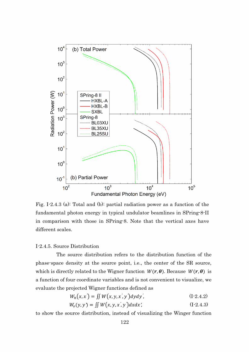
122
Fig. I-2.4.3 (a): Total and (b): partial radiation power as a function of the fundamental photon energy in typical undulator beamlines in SPring-8-II in comparison with those in SPring-8. Note that the vertical axes have different scales. I-2.4.5. Source Distribution
The source distribution refers to the distribution function of the phase-space density at the source point, i.e., the center of the SR source, which is directly related to the Wigner function 𝑊(𝒓,𝜽). Because 𝑊(𝒓,𝜽) is a function of four coordinate variables and is not convenient to visualize, we evaluate the projected Wigner functions defined as 𝑊ℎ�𝑥, 𝑥 ′� = ∬𝑊�𝑥,𝑦, 𝑥 ′,𝑦 ′�𝑑𝑦𝑑𝑦 ′, (I-2.4.2) 𝑊𝑣(𝑦,𝑦′) = ∬𝑊�𝑥,𝑦, 𝑥 ′, 𝑦 ′�𝑑𝑥𝑑𝑥′, (I-2.4.3) to show the source distribution, instead of visualizing the Winger function
123
𝑊(𝒓,𝜽). The functions 𝑊ℎ and 𝑊𝑣 give the source distributions in the horizontal and vertical phase spaces, if 𝑊(𝒓,𝜽) can be approximated by the decoupled form defined by
𝑊𝑑 = 𝑊ℎ𝑊𝑣𝐹
, (I-2.4.4)
where 𝐹 denotes the effective total flux obtained by integrating 𝑊(𝒓,𝜽) over the whole phase. In practice, this approximation is usually valid under the practical condition that the electron beam emittance is larger than, or at least comparable to the optical emittance of diffraction-limited light [Tanaka2014]. In what follows, the source distributions in the horizontal and vertical phase spaces are evaluated using these two functions.
Figures. I-2.4.4~I-2.4.6 show the comparisons of the source distributions for the three beamline HXBL-A, SXBL, and BM2 in SPring-8-II, with those for BL03XU, BL25SU, and BM2 in SPring-8, respectively. In each figure, (a) and (c) denote the distributions in the horizontal and vertical phase space for the SPring-8-II beamlines, while (b) and (d) denote those for the SPring-8 beamlines.
Figure I-2.4.4 shows the source distributions for HXBLs at the photon energy of 10 keV. The comparison between (a) and (b) indicates a significant improvement of the source size (width in the x direction) and a slight improvement of the angular divergence (width in the x’ direction) in the horizontal direction, which comes from the reduction of the horizontal emittance and betatron function. On the other hand, the vertical source size and angular divergence becomes slightly larger, as found from the comparison between (c) and (d). This reflects the larger coupling constant (and vertical emittance) of SPring-8-II than that of SPring-8.

124
Fig. I-2.4.4: Source distributions for HXBLs at 10 keV.
It is interesting to note that the vertical source distribution is slightly different from a Gaussian function as opposed to the horizontal one. This derives from the fact that the Wigner function of UR from a single electron is far from a Gaussian function. Because of the low emittance in the vertical direction, the original non-Gaussian profile survives even after convolution with the Gaussian distribution function of the electron beam.
Figure I-2.4.5 shows the source distributions for SXBLs at the photon energy of 500 eV. As in the case of HXBLs, the horizontal source size is significantly improved, while the other properties do not change largely. This means that the electron beam properties except the horizontal beam size do not contribute to the source distribution in this condition. Also note that the non-Gaussian nature of the vertical source distribution as shown in (c) and (d) is more pronounced. This may have to be taken into account for designing the optical elements in the SXBLs.
125
Fig. I-2.4.5: Source distributions for SXBLs at 500 eV.
Fig. I-2.4.6: Source distributions for BMBLs at 10 keV.
126
Figure I-2.4.6 shows the source distributions for BMBLs at the photon energy of 10 keV with the horizontal aperture of 0.1 mrad. The comparison between (a) and (b) indicates a significant improvement of the angular divergence as well as the source size in the horizontal direction. Not only the emittance reduction but also the modification of the betatron function contributes to this improvement. In the vertical direction, the source size is reduced as well, while the angular divergence grows. Note that both of them are not related to the emittance change. The former comes from the shorter betatron function, while the latter comes from the reduced electron energy: the angular divergence of BM radiation is inversely proportional to the Lorentz factor. I-2.4.6. Transverse Coherence
The source distribution presented in the former section can be extended to a more quantitative discussion in terms of the transverse coherence.
In general, the degree of transverse coherence 𝜇 is given as a function of two different points 𝒓1 and 𝒓2 and thus is not convenient to describe the light source performance. We thus introduce the overall degree of coherence ζ instead of 𝜇(𝒓1,𝒓2) , in order to denote the coherence property in a specific beamline, which is actually defined as a spatial average of 𝜇2(𝒓1,𝒓2), and can be computed using the Wigner functions as follows [Bazarov2012]
ζ = �𝜆𝐹�2∬𝑊2(𝒓,𝜽)𝑑𝒓𝑑𝜽. (I-2.4.5)
Assuming that the Wigner function can be decoupled, ζ is also given as a decoupled form ζ = ζ𝑥ζ𝑦, where
ζ𝑥 = 𝜆𝐹2 ∬𝑊ℎ
2�𝑥, 𝑥 ′�𝑑𝑥𝑑𝑥 ′, (I-2.4.6)
and
ζ𝑦 = 𝜆𝐹2 ∬𝑊𝑣
2(𝑦,𝑦′)𝑑𝑦𝑑𝑦′, (I-2.4.7)
are referred to as horizontal and vertical degrees of coherence.
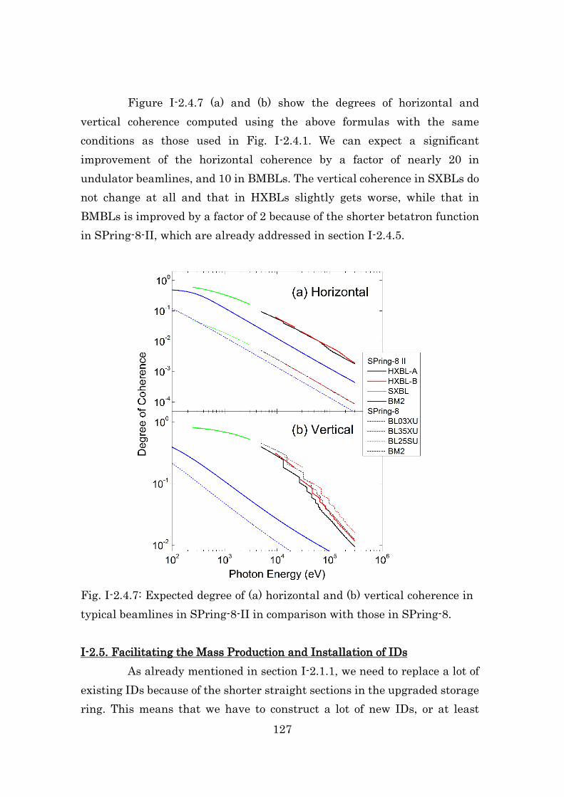
127
Figure I-2.4.7 (a) and (b) show the degrees of horizontal and vertical coherence computed using the above formulas with the same conditions as those used in Fig. I-2.4.1. We can expect a significant improvement of the horizontal coherence by a factor of nearly 20 in undulator beamlines, and 10 in BMBLs. The vertical coherence in SXBLs do not change at all and that in HXBLs slightly gets worse, while that in BMBLs is improved by a factor of 2 because of the shorter betatron function in SPring-8-II, which are already addressed in section I-2.4.5.
Fig. I-2.4.7: Expected degree of (a) horizontal and (b) vertical coherence in typical beamlines in SPring-8-II in comparison with those in SPring-8. I-2.5. Facilitating the Mass Production and Installation of IDs
As already mentioned in section I-2.1.1, we need to replace a lot of existing IDs because of the shorter straight sections in the upgraded storage ring. This means that we have to construct a lot of new IDs, or at least
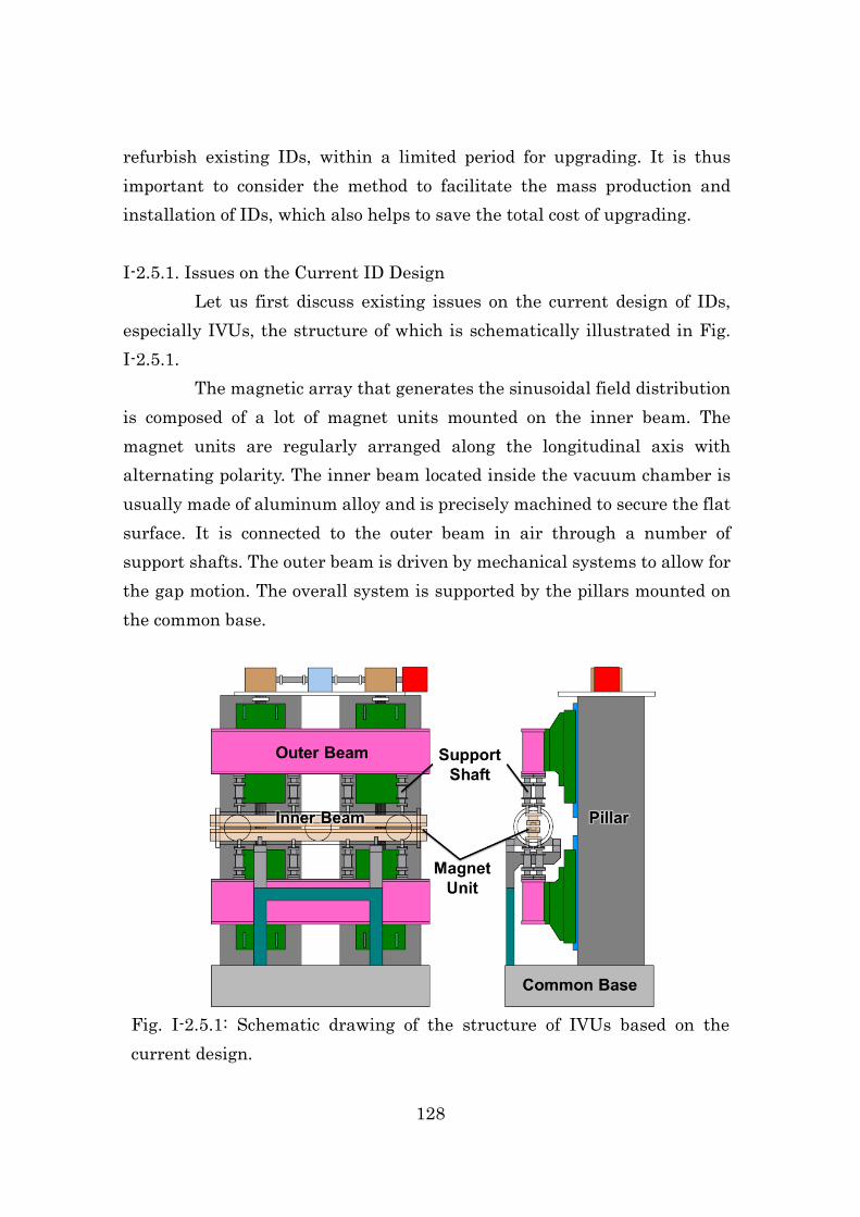
128
refurbish existing IDs, within a limited period for upgrading. It is thus important to consider the method to facilitate the mass production and installation of IDs, which also helps to save the total cost of upgrading. I-2.5.1. Issues on the Current ID Design
Let us first discuss existing issues on the current design of IDs, especially IVUs, the structure of which is schematically illustrated in Fig. I-2.5.1.
The magnetic array that generates the sinusoidal field distribution is composed of a lot of magnet units mounted on the inner beam. The magnet units are regularly arranged along the longitudinal axis with alternating polarity. The inner beam located inside the vacuum chamber is usually made of aluminum alloy and is precisely machined to secure the flat surface. It is connected to the outer beam in air through a number of support shafts. The outer beam is driven by mechanical systems to allow for the gap motion. The overall system is supported by the pillars mounted on the common base.
Fig. I-2.5.1: Schematic drawing of the structure of IVUs based on the current design.
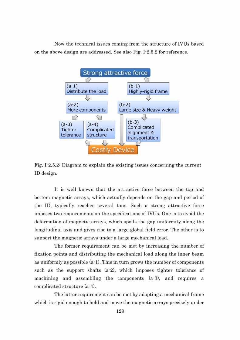
129
Now the technical issues coming from the structure of IVUs based on the above design are addressed. See also Fig. I-2.5.2 for reference.
Fig. I-2.5.2: Diagram to explain the existing issues concerning the current ID design.
It is well known that the attractive force between the top and
bottom magnetic arrays, which actually depends on the gap and period of the ID, typically reaches several tons. Such a strong attractive force imposes two requirements on the specifications of IVUs. One is to avoid the deformation of magnetic arrays, which spoils the gap uniformity along the longitudinal axis and gives rise to a large global field error. The other is to support the magnetic arrays under a large mechanical load.
The former requirement can be met by increasing the number of fixation points and distributing the mechanical load along the inner beam as uniformly as possible (a-1). This in turn grows the number of components such as the support shafts (a-2), which imposes tighter tolerance of machining and assembling the components (a-3), and requires a complicated structure (a-4).
The latter requirement can be met by adopting a mechanical frame which is rigid enough to hold and move the magnetic arrays precisely under

130
the strong attractive force (b-1). As a result, the mechanical frame becomes necessarily large and massive (b-2), which requires complicated procedures for alignment and transportation of the device (b-3). I-2.5.2. Structural Reform
All the problems explained in the previous section obviously come from the strong attractive force. In other words, we can expect a better solution, if the attractive force can be cancelled by some means. To be more specific, the mechanical frame can be much lighter, simpler, and more cost-effective, because it does not have to be too rigid any longer. Such a structural reform of IDs will contribute to shortening the lead time for the mass production and facilitating the transportation and alignment.
The key issue toward the structural reform is the development of the system to cancel the attractive force over the whole operational gap range. We need to generate a repulsive force which depends on the gap identically to the attractive force by the ID magnet array, which is actually an exponential function of the gap.
Fig. I-2.5.3: Possible solutions to cancel the attractive force of ID magnetic
arrays: (a) mechanical and (b) magnetic.
(b)(a)

131
Figure I-2.5.3 (a) shows a mechanical system based on springs attached to the both ends of the magnetic array to cancel the attractive force. Note that the repulsive force of the springs should be nonlinear (exponential), which is not easily fabricated. An alternative way based on the combination of a number of springs with different properties [Marcouillé2010] may help. In any case, we have a concern about the long-term stability of springs. In addition, precise field measurement, which is indispensable for the field correction process of IDs, is another challenge under the enclosed environment.
Another way as shown in Fig. I-2.5.3 (b) is to take advantage of the magnetic system, in which additional magnetic arrays to generate a repulsive force are attached to the main (central) magnetic array. The additional magnetic arrays should have the same magnetic properties as the main one, so that the attractive force is cancelled. In principle, this method will completely cancel the attractive force. It should be noted, however, that we need four more magnetic arrays in addition to the two main ones, which considerably increases not only the total cost but also the number of processes for manufacturing the IDs.
In order to overcome the above difficulty toward realization of the attractive force cancellation system, a new approach is under investigation, which is based on the magnetic method but is much more cost-effective than the above scheme. In a couple of years, we will demonstrate the new system and then build a prototype device based on it, toward the structural reform of IDs in prospect of utilization in SPring-8-II. I-2.5.3. Revision of the Field Correction Procedure
The field correction is an important process to eliminate the unwanted effects due to magnetic errors, which requires a precise measurement of the field distribution. For this purpose, the ID is usually transported to the field measurement laboratory which is equipped with a number of magnetic sensors and several multi-axis actuation stages to move the sensors precisely. Then alignment of the ID and measurement instrument is made to perform a precise and reliable measurement.

132
In the mass production of IDs for SPring-8-II, we need to repeat the field correction process so many times. To be specific, after completing the field correction, the ID is taken away from the measurement laboratory to be installed in the accelerator tunnel, or moved to the storage area. Then next ID is installed in the laboratory to continue the field correction.
In the above process, we waste a lot of time: during the installation and alignment of the ID in the laboratory, the measurement apparatus is not available and the field correction process stops.
One idea to reduce the waste of time in the field correction process is to install a kind of mechanical frame dedicated to the field correction in the measurement laboratory. After completing the field correction of a specific ID, we replace only the magnetic arrays without moving the mechanical frame. Then the time for installation and alignment is no longer necessary, which will significantly save the lead time for mass production of IDs.
In the above scheme, we have a concern that the global field error is induced in the final manufacturing process in which the magnetic array is assembled in the other mechanical frame to be actually used. The alignment accuracy of the support shafts that hold the magnetic array cannot be better than several microns at the best of times, which can lead to a long-range gap variation along the longitudinal axis. This kind of global error can give rise to relatively a large phase error and significant degradation of the available flux.
In order to solve the above problem, it is necessary to measure the field distribution after assembly and correct the global error if necessary. This requires a portable field measurement system and adjustable support shafts, which are already developed in SPring-8 and already applied to the field correction in CPMUs [Tanaka2009]. I-2.6. Summary
In this report, we have described the specifications and performances of new IDs to be replaced with the existing ones. We have another option to keep on using them after a minor or major revision.

133
The minor revision refers to the refurbishment only to fit the new straight section. The magnetic arrays, vacuum equipment, and mechanical components are disassembled first and then assembled again with reduced number of components to shorten the whole length. In the major revision, the magnetic arrays are renewed to have the optimized period in addition to the refurbishment above.
It should be noted that we are not sure about the total cost and lead time necessary for the above revision, even minor one, because the structure of the existing IDs is quite complicated as already mentioned and requires a careful alignment to restore the original performance. The final decision should be made comprehensively with all the related issues taken into account. References [Bazarov2012] I. V. Bazarov, Phys. Rev. ST-AB, 15, 050703 (2012). [Bizen2003] T. Bizen et al., Nucl. Instr. and Meth. A515, 850 (2003). [Chubar1998] O. Chubar et al., J. Synchrotron Radiation 5, 481 (1998). [Hara1998a] T. Hara et al., J. Synchrotron Rad., 5, 403 (1998). [Hara1998b] T. Hara et al., J. Synchrotron Rad., 5, 426 (1998). [Hara2004] T. Hara et al., Phys. Rev. ST-AB 7, 050702 (2004). [Kim1989] K. J. Kim, AIP Conf. Proc. 184, 565 (1989). [Kuroda2013] A. Kuroda et al., Proc. 10th PASJ Meeting, 897 (2013). [Marcouillé2010] O. Marcouillé et al., Proc. IPAC’10, 3104 (2010). [Sasaki1993] S. Sasaki et al., Nucl. Instrum. and Meth., A331, 763 (1993). [Shirasawa2003] K. Shirasawa et al. Proc. SRI2003, 191 (2003). [Tanaka1995] T. Tanaka et al., Nucl. Instrum. and Meth., A364, 368 (1995). [Tanaka2001] T. Tanaka et al., J. Synchrotron Rad., 8 (2001) 1221. [Tanaka2002] T. Tanaka et al., Nucl. Instrum. Meth., A490, 583 (2002). [Tanaka2009] T. Tanaka et al., Phys. Rev. ST-AB, 12, 120702 (2009). [Tanaka2011a] T. Tanaka et al, presented in 24th JSSRR Annual Meeting, Tsukuba (2011) (unpublished). [Tanaka2011b] T. Tanaka et al., Nucl. Instrum. and Meth., A659, 537 (2011). [Tanaka2014] T. Tanaka, Phys. Rev. ST-AB, accepted for publication.

134
PART-I I-3 Control System
I-3.1. Design Overview I-3.2. Computing and Network I-3.3. Accelerator Equipment Controls I-3.4. Beamline Control I-3.5. Safety Interlock
135
I-3. Control System I-3.1. Design Overview
The accelerator control system for the SPring-8-II storage ring is designed on the basis of the current control framework, MADOCA [Tanaka1997], with adding the state-of-the-art technologies. The MADOCA control framework was developed originally at SPring-8, and has been stably working for more than seventeen years as a keystone in order to control accelerators and beamlines. Recently, MADOCA messaging scheme was upgraded with ZeroQM middleware to handle variable data structure with no limitation of a carrying data size [Matsumoto2013]. And also, the new scheme supports Windows operation system (OS) in addition to the UNIX OS families. Application field of MADOCA is now extended to the experimental data-acquisition system in SACLA/XFEL in SPring-8.
The cutting edge technologies on the information and the electronics systems in the market have been making progress rapidly. In the design of SPring-8-II control system, we keep the reliable control components with good record in our operation experience. On the other hand, we will not use some components such as fairly out-of-date maintainability or less performance below the required level. Thee-tier control architecture is kept on the bases of distributed control architecture of MADOCA with considering continuity of the facility sustainability. The resources ever developed so far in SPring-8 will be re-used as much as possible both on software and hardware for the compatibility and quick construction of the control and operation system.
We keep the relational database management system (RDBMS) for the machine configuration data, and also adopt Key-Value Store (KVS) to handle the machine logging data [Kago2013]. A high-speed network with wide bandwidth and low latency plays a middleware physical layer between operator consoles and equipment device controllers. The network is built by using Ethernet technology that is properly segmented and aggregated. Firewalls are suitably installed for interconnection between network segments to guarantee access control and security with sufficient
136
bandwidth. Control components are selected to fit each accelerator sub-system on the classification of three levels of control processing performance; i.e. slow, medium and fast. We deploy the commercial off-the-shelf (COTS) products as the building blocks of the control system as much as possible in order to minimize construction cost and development task/risk.
A programmable logic controller (PLC) will be used for the slow control subsystems because of easy installation and maintenance. The VMEbus systems still survive as the well-established system that has been proven during the long duty operation in the current SPring-8. The VME will be adopted as a medium speed controller with many of re-usable software libraries ever built, which will reduce the production time and effort.
Recently, the demands on higher performance of digital data processing has been growing up, especially at low level RF (LLRF) control, waveform data handling/analysis and experimental data processing. The telecommunication packet transaction in the market needs ultra-fast digital-data processing at the huge scale of communication digital data. Hence, the data handling in this field requires high-bandwidth cutting-edge technology necessarily. The emerging technology such as TCA (Telecommunications and Computing Architecture) is promising as a candidate of the high-end control platform. The TCA system carries advanced mezzanine cards (AMC) that are expected to satisfy the high level requirements of the digital data processing.
In this section, the design of control system of accelerator, beamline, computing, network, utilities and safety interlock are described. I-3.2. Computing and Network
Reliability is important for the computing and network system as the elements of the controls, such as database and file servers, operation consoles, and backbone networks. To enhance reliability, we introduce virtualization technology for various layers of the computing systems including communication over network, operating system, middleware, and

137
application software beyond the hardware physical boundaries. By applying the virtualization technology, we can suppress the system proliferation, and expect cost effectiveness and low power consumption consequently. I-3.2.1. Server System
To achieve 24h365d availability as high enough, computer hardware will be settled concentrating into a computer room, which is equipped with CVCF power supply system and protected by voltage-drop-compensated electrical power. Database Server:
The Sybase, a commercial enterprise RDBMS, has been storing many signal points since 1997. The signals are not only the status of accelerator components, but also the facility status such as air conditioner, cooling water, and electrical powers. The RDBMS has been playing the essential role for the data management in SPring-8 by the standard SQL data-access to the relational schema.
Recently, Key-Value Store has been growing up at the market especially for the big data handling. The KVS that provides NoSQL data access, is suitable for handling of the chronological logging data. Hence, the KVS will be used to manage the on-line and archive database of the machine status logging. The RDBMS is kept to manage the machine configuration data. A promising database scheme by using KVS will consist of a combination of Redis and Cassandra that is under development in SPring-8 [Kago2013]. The KVS computer system will be composed of a group of PC assuring redundancy by the quorum determination method. File Server:
Both high IOPS performance and high capacity are required for file server, because the file server stores many file types, such as source code repository, binaries including middleware libraries, and disk image of virtual machines. To satisfy the requirements, the file server will be hierarchical storage using both non-volatile memory and high-capacity
138
magnetic hard disk. Most of computing system will be virtualized using hypervisor
and/or container technologies. By using virtualization, we can reduce the number of hardware, and improve availability simultaneously.
All network connections in the computer room will be based on 10-giga-bit Ethernet (10GbE) or wider bandwidth Ethernet. In the case of low-latency control performance such as fast feedback or correction, the InfiniBand will be an alternative choice for interconnection. I-3.2.2. Central Control Room
Thin client and virtual desktop technology will be used for operator consoles. Using the thin client with virtualized computers in the computer room, we can improve electric-power consumption. The virtualization technology also improves availability of the operator consoles. A large-sized screen, display wall, will be kept at the front of the control room. Operating status and alarms are displayed on the screen for information sharing by operators. I-3.2.3. Network System
The site-wide network system will be applied virtualization technology to reduce physical devices and to improve reliability. A 10GbE or wider bandwidth Ethernet will be used for trunk route of physical network. Logical networks, such as accelerator control, experimental control, and experimental data transfer, are segmented and established on the physical network. Performance of each logical network will be guaranteed using quality-of-service technology. For the access control, firewalls will be installed suitably between the logical networks. I-3.2.4. Software
The Linux OS family and Solaris that we have been using for the long time have proven its reliability by ever-lasting good records. The continuity of the same OS will be the keystone of the compatibility for a bunch of running application software. For the core software frameworks, C
139
and C++ standardized computer languages are chosen to guarantee long-term development.
In addition to the C and the C++ languages, script languages and visualized languages, such as Python and LabVIEW, will be offered to users for beamline components and experimental station control [Furukawa2013]. By using the latest MADOCA II framework, users can use Windows PC directly to operate the beamline components seamlessly, which had not been supported. To maintain code quality, static and dynamic program analysis tools will be offered. All versions of source codes and binaries are archived in the file server. I-3.3. Accelerator Equipment Controls
An interface from the control system to the accelerator equipment will be a mixture of the Programmable Logic Controller and the High Speed Serial Bus System such as MTCA.4 or ATCA, and the VME system. Each platform will be adopted on the concept of right platform in the right place. The PLC will be used for the slow control system for rigid control such as PID control and local device interlocks. The sequence control of PLC is firm and robust enough to support device interlock and radiation safety interlock too. The PLC can be used with Devicenet and/or EtherCAT field bus interface if it is necessary [EtherCAT_URL]. For the high-speed signal processing such as the low-level RF control and the beam monitor system, and trigger signal distribution, we will use the xTCA platform implemented with the A/D, D/A and FPGA, where the TCA platform family is noted as xTCA. One standard of the xTCA, micro-TCA, showed good performance as applied to the measurement of the electron beam emittance by using interferometer [Kiyomichi2013]. The VME system will be re-used for slow or medium speed control. We have many of well-established software libraries that are necessary to control the wide variety of VME I/O boards by using device drivers and application program interfaces. I-3.3.1. Vacuum System Control
To control the vacuum system including device interlock, a PLC
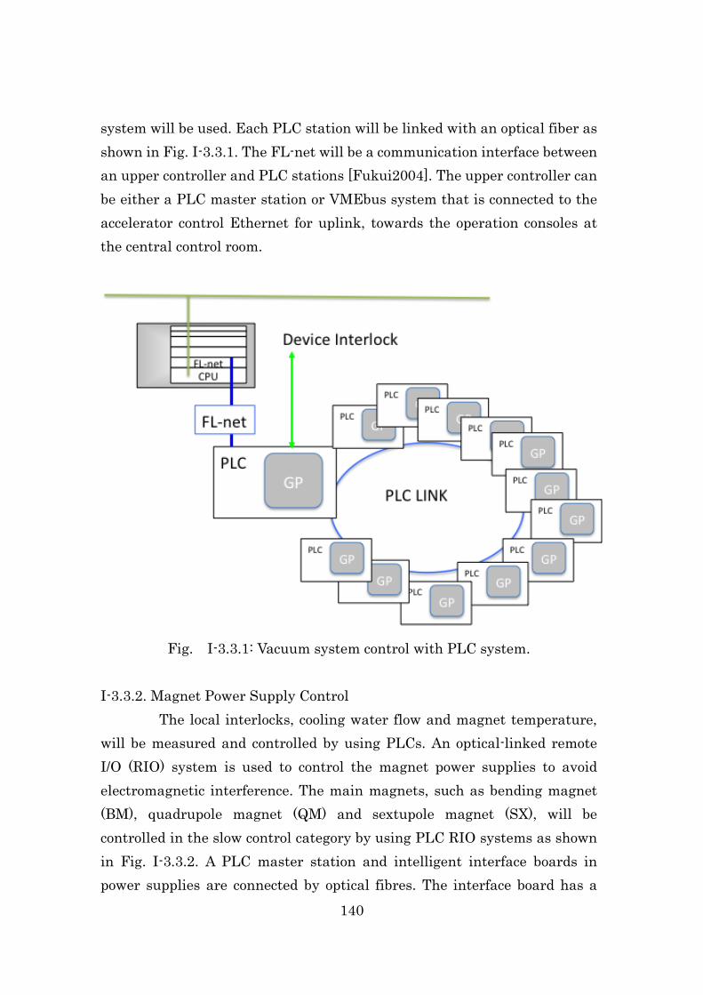
140
system will be used. Each PLC station will be linked with an optical fiber as shown in Fig. I-3.3.1. The FL-net will be a communication interface between an upper controller and PLC stations [Fukui2004]. The upper controller can be either a PLC master station or VMEbus system that is connected to the accelerator control Ethernet for uplink, towards the operation consoles at the central control room.
Fig. I-3.3.1: Vacuum system control with PLC system. I-3.3.2. Magnet Power Supply Control
The local interlocks, cooling water flow and magnet temperature, will be measured and controlled by using PLCs. An optical-linked remote I/O (RIO) system is used to control the magnet power supplies to avoid electromagnetic interference. The main magnets, such as bending magnet (BM), quadrupole magnet (QM) and sextupole magnet (SX), will be controlled in the slow control category by using PLC RIO systems as shown in Fig. I-3.3.2. A PLC master station and intelligent interface boards in power supplies are connected by optical fibres. The interface board has a

141
FPGA chip that stores a pre-defined control sequence of a power supply. The sequence is reconfigurable by installing an operation algorithm on the chip, and can be driven by the control commands issued from operator consoles. The response time is a millisecond or less when there are assuming two or more magnet power supplies in operation at the same time.
Fig. I-3.3.2: Magnet power-supply control by intelligent interface cards.
For a set of permanent magnets that are optional design of BM, the movable outer plate will be controlled by PLC with the pulse motor controller via the field bus to reduce the number of cablings. Because of the temperature dependence of magnetic field, we will measure magnet temperature with high precision of 0.01 degree. We need a fast control system for the power supplies of steering magnets (ST) and auxiliary power supplies of QM because of COD correction and tune correction of stored electron beams with feedback rate of 100Hz or faster. I-3.3.3. RF System Control
Figure I-3.3.3 shows a schematic view of the RF control system. A signal processing board will be designed with the high speed AD / DA and FPGA with the function of a digital down conversion to provide the amplitude and phase control for the acceleration cavities. The xTCA platform is suitable to handle the RF digital signals of low-level control components with better performance than the current NIM and VMEbus
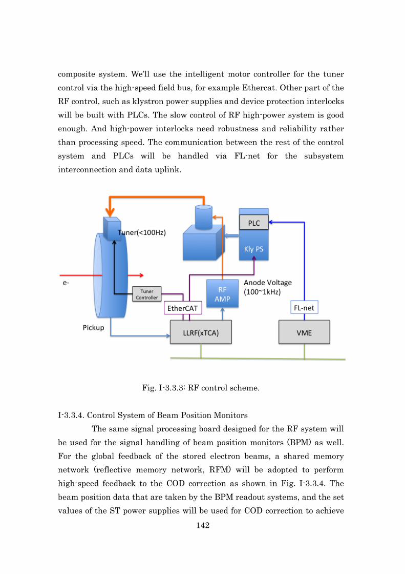
142
composite system. We’ll use the intelligent motor controller for the tuner control via the high-speed field bus, for example Ethercat. Other part of the RF control, such as klystron power supplies and device protection interlocks will be built with PLCs. The slow control of RF high-power system is good enough. And high-power interlocks need robustness and reliability rather than processing speed. The communication between the rest of the control system and PLCs will be handled via FL-net for the subsystem interconnection and data uplink.
Fig. I-3.3.3: RF control scheme.
I-3.3.4. Control System of Beam Position Monitors
The same signal processing board designed for the RF system will be used for the signal handling of beam position monitors (BPM) as well. For the global feedback of the stored electron beams, a shared memory network (reflective memory network, RFM) will be adopted to perform high-speed feedback to the COD correction as shown in Fig. I-3.3.4. The beam position data that are taken by the BPM readout systems, and the set values of the ST power supplies will be used for COD correction to achieve
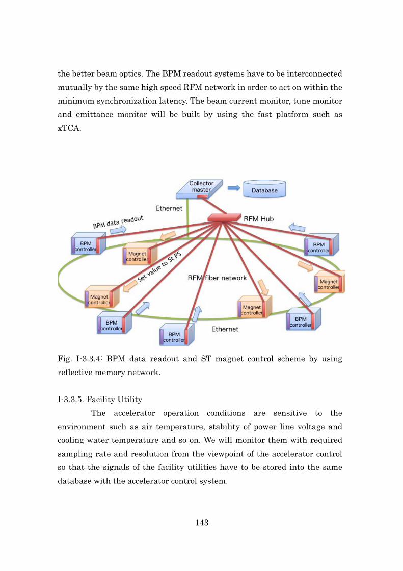
143
the better beam optics. The BPM readout systems have to be interconnected mutually by the same high speed RFM network in order to act on within the minimum synchronization latency. The beam current monitor, tune monitor and emittance monitor will be built by using the fast platform such as xTCA.
Fig. I-3.3.4: BPM data readout and ST magnet control scheme by using reflective memory network. I-3.3.5. Facility Utility
The accelerator operation conditions are sensitive to the environment such as air temperature, stability of power line voltage and cooling water temperature and so on. We will monitor them with required sampling rate and resolution from the viewpoint of the accelerator control so that the signals of the facility utilities have to be stored into the same database with the accelerator control system.

144
I-3.4. Beamline Control A beamline control system, which controls an insertion device (ID),
frontend components and a monochromator, is installed for each beamline [Ohata2001]. The beamline control system consists of two VME systems and a PC for operation. One VME system controls ID and the other one is for the control of the rest of beamline components. The control framework MADOCA connects the VME controllers and the PC over the network. However, it is difficult to synchronize the ID gap and the monochromator using the Ethernet.
Fig. I-3.4.1: A design of beamline control system for synchronizing the ID, the monochromator, and detectors.
The following new functions are required for SPring-8-II in order to use the brilliant light effectively: (a) Synchronous control of the gap of the ID and the monochromator. (b) Synchronous control of the monochromator and the detector.

145
The function (a) enables the effective use of the SR light because
user does not have to wait for satisfying both the monochromator and ID gap when user changes the photon energy. The ID gap is always kept by the appropriate value with the monochromator. The function (b) enables the quick-scan with changing the monochromator settings, which shorten a time required for the measurement of energy distribution such as XAFS experiment.
In order to realize the new functions, we designed a new beamline control system as shown in Fig. I-3.4.1. We will install a synchronous control system that consists of a BL sync master, some of slave stations and a fast field bus. The slaves control the ID gap, steering magnets for the ID, pulse motors of the monochromator and triggers for the detectors. The length of the filed bus is necessary for about 100m, and the system has to achieve the synchronization of the gap and monochromator control within 1ms. I-3.5. Safety Interlock
A safety interlock system protects users from radiation hazards induced by electron beam and synchrotron radiations. The schematic view of the safety interlock system for SPring-8-II is shown in Fig. I-3.5.1 The system is composed of accelerator safety interlock systems and beamline interlock systems. The accelerator safety interlock system based on the “area interlock” concept established in 2010 will be utilized [Saji2009]. Each area interlock system monitors the status of safety components and controls the permission signal for the RF located in each area according to the safety condition of the area. The gun permission signal is sent to the gun safety interlock. When all gun permissions are established, the gun safety interlock system permits the gun operation.
The beamline interlock system controls the doors of experimental hutches, beam shutters, and so on [Matushita2001]. When the safety condition is not established, the beamline interlock system closes and locks the beam shutter. In the case of emergency, the beamline interlock system
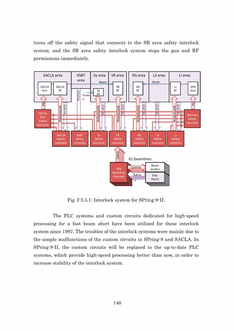
146
turns off the safety signal that connects to the SR area safety interlock system, and the SR area safety interlock system stops the gun and RF permissions immediately.
Fig. I-3.5.1: Interlock system for SPring-8-II.
The PLC systems and custom circuits dedicated for high-speed processing for a fast beam abort have been utilized for these interlock system since 1997. The troubles of the interlock systems were mainly due to the simple malfunctions of the custom circuits in SPring-8 and SACLA. In SPring-8-II, the custom circuits will be replaced to the up-to-date PLC systems, which provide high-speed processing better than now, in order to increase stability of the interlock system.

147
References [EtherCAT_URL] http://www.ethercat.org/en/technology.html [Fukui2004] T. Fukui et al., Proc. of PCaPAC2005, Hayama, Japan, 2004. [Furukawa2013] Y. Furukawa et al., Proc. of ICALEPCS2013, San Francisco, USA, 410 (2013). [Kago2013] M. Kago and A. Yamashita, Proc. of ICALEPCS2013, San Francisco, USA, 532 (2013). [Kiyomichi2013] A. Kiyomichi et al., Proc. of ICALEPCS2013, San Francisco, USA, 786 (2013). [Matsumoto2013] T. Matsumoto et al., Proc. of ICALEPCS2013, San Francisco, USA, 944 (2013). [Matushita2001] T. Matsushita et al., Nucl. Inst. and Meth. in Physics Res. A, 467-468 (2001) 816. [Ohata2001] T. Ohata et al., Nucl. Instrum. Methods 467 (2001) 820. [Saji2009] C. Saji et al., Proc. of ICALEPCS2009 (2009); M. Kago et al., Proc. of ICALEPCS2009 (2009); M. Kago et al., Proc. of IPAC’10, (2010). [Tanaka1997] R. Tanaka et al., Proc. of ICALEPCS1997, Beijing, China, 1 (1997).

148
PART-I I-4 Safety Issues
I-4.1. Introduction I-4.2. Radiation Shielding I-4.3. Safety System I-4.4. Induced Activity and the Radioactive Waste I-4.5. Summary

149
I-4.1. Introduction Since 1997, SPring-8 has been operated constantly with 8GeV
electrons without serious radiation problems, and the top-up operation for the steady stored current at the storage ring has been conducted from 2004[Tanaka2004], [Asano2007] . Radiation safety systems and radiation shielding have been operated and placed without significant changes from the beginning of the operation till now. In addition, the injection efficiency has been much improved rather than the initial establishments. However it is required to reassess the radiation shielding condition in occasion of the upgrade of SPring-8 to obtain the low emittance of the diffraction limit with 6 GeV electrons without changing the bulk shield, because of the expectation of severe conditions due to the larger quantity of the electron injection required to correct the deficit for prospective much shorter life time. Skyshine dose re-estimation is also required because the dose criterion at the site boundary has also a strong influence on the shielding conditions. A large amount of radioactive waste due to the dismantling of the existing storage ring will be produced so that the precious estimation of the induced activities is required strongly.
During the past 10 years, the simulation techniques have been improved drastically by using Monte Carlo methods, therefore the reassessments of shielding design should be performed by using these updated methods as much as possible [Asano2013] .
I-4.2. Radiation Shielding
For the SPring-8-II design, the upgrade of the bulk shield of the ring must be avoided as much as possible. Figure I-4.2.1 shows the design of the storage ring of SPring-8, and the shield thicknesses of the side wall are 1 m and 1.65 m ordinary concretes for normal section and injection section, respectively. The ratchet walls of the storage ring are made of 0.65 m ordinary concrete and 0.15 m lead. The largest possible number of the accelerated electron should be injected into the ring on the conditions. To do this, it is required to reassess the beam loss scenario with the shorter life time on the basis of the present design criteria and detailed analyses.

150
Fig. I-4.2.1: Drawing of the storage ring building and the experimental hall. I-4.2.1. Design Criteria
On the basis of ALARA principle and the Japanese law for the prevention from radiation hazards, the design criteria of the SPring-8 site was authorized as follows [Sasamoto1994] , (1) For radiation workers, the dose must be less than 50 mSv for every year
(25 μSv/h for 40 hours per week) and 100 mSv for every five years in the law so that the design criteria were decided to be 8μSv/h ( 25μSv/h *1/3)
(2) At the boundary of radiation controlled area, the dose must be less than 1.3mSv for every three months (2.5μSv/h ) and the design criteria are the same.
(3) At the site boundary, the dose must be less than 250μSv for every three months, and the design criteria of the external dose were decided to be 50μSv for every year.
I-4.2.2. Design Methods
For the shielding design of SPring-8, we employed the Swanson’s [Swanson1979] and Jenkins’ [Jenkins1979] formula for forward and lateral directions of the bulk shield, respectively. After the beginning of the operation, the shielding calculation methods have been improved drastically

151
such as Monte Carlo simulation codes [Asano2013]. In addition to these above mentioned formula, we have been mainly using the EGS4 [Nelson1985] and FLUKA [Fasso2005] Monte Carlo codes, and the SHIELD 11 [Nelson2005] empirical adjustment code, and the calculation results of the codes are shown in Fig. I-4.2.2. As shown in the figures, the target geometry is sensitive so that it must be treated carefully.
Fig. I-4.2.2: Inter-comparison of leakage dose calculations between Jenkins’ formula, SHIELD 11 and FLUKA. Left and right hand figures are for gamma and neutron leakage dose, respectively. Black solid lines are the results of Jenkins calculations, Blue lines are SHIELD 11 and blue diamonds are SHIELD11 without considering the self-shielding of the target. Red dots are FLUKA calculations. Target and its size were assumed as iron and 20cm thick. The shield wall is made of ordinary concrete with 1m in thickness.
I-4.2.3. Beam Loss Scenario
The present capacity of the beam operation of the storage ring is as follows: maximum electron energy, maximum stored power, and maximum stored electrons are 8 GeV, 7.6 kJ, and 2.4 x10¹³, respectively. And we have now four operation modes, these are tuning, stored injection, storage with decay, and top-up with steady stored current modes. For each mode, maximum permissible electron injection numbers are as follows, 1.8x10¹⁴
e/w and 1.5x10¹⁵ e/3M for tuning, 3.8x10¹⁴ e/w and 3.1x10¹⁵e/3M for stored
60 80 100 12010–8
10–7
10–6
10–5
Scattering angle(deg.)
Leak
age
gam
ma
dose
(pSv
/ele
ctro
n)
6GeV electron1m shield (O.C.)
60 80 100 12010–8
10–7
10–6
10–5
Scattering angle(deg.)
Leak
age
neut
ron
dose
(pSv
/ele
ctro
n)
6GeV electron1m shield (O.C.)
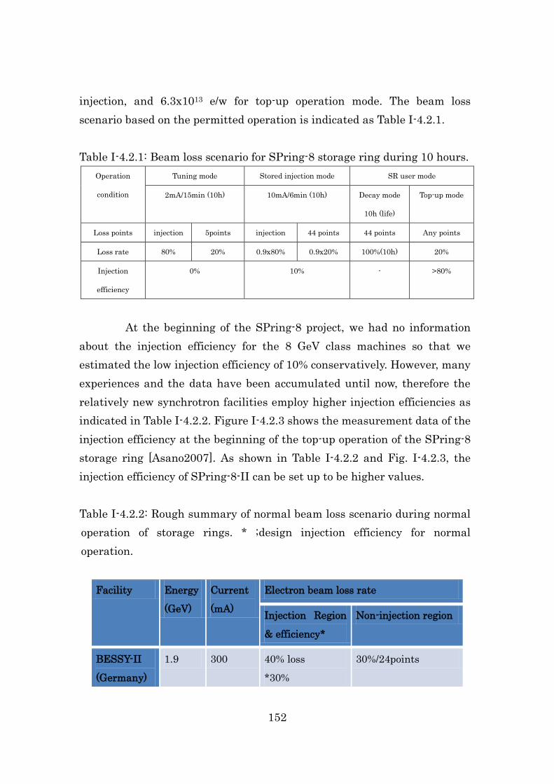
152
injection, and 6.3x10¹³ e/w for top-up operation mode. The beam loss scenario based on the permitted operation is indicated as Table I-4.2.1.
Table I-4.2.1: Beam loss scenario for SPring-8 storage ring during 10 hours.
Operation
condition
Tuning mode Stored injection mode SR user mode
2mA/15min (10h) 10mA/6min (10h) Decay mode
10h (life)
Top-up mode
Loss points injection 5points injection 44 points 44 points Any points
Loss rate 80% 20% 0.9x80% 0.9x20% 100%(10h) 20%
Injection
efficiency
0% 10% - >80%
At the beginning of the SPring-8 project, we had no information
about the injection efficiency for the 8 GeV class machines so that we estimated the low injection efficiency of 10% conservatively. However, many experiences and the data have been accumulated until now, therefore the relatively new synchrotron facilities employ higher injection efficiencies as indicated in Table I-4.2.2. Figure I-4.2.3 shows the measurement data of the injection efficiency at the beginning of the top-up operation of the SPring-8 storage ring [Asano2007]. As shown in Table I-4.2.2 and Fig. I-4.2.3, the injection efficiency of SPring-8-II can be set up to be higher values.
Table I-4.2.2: Rough summary of normal beam loss scenario during normal operation of storage rings. * ;design injection efficiency for normal operation.
Facility Energy
(GeV)
Current
(mA)
Electron beam loss rate
Injection Region
& efficiency*
Non-injection region
BESSY-II
(Germany)
1.9 300 40% loss
*30%
30%/24points

153
TLS (Taiwan)
1.5 200 35% loss *30%
35%ring uniformly
SSRL (U.S.A.)
3 500 16mW *75%
56mW/28points, 50mW at Dump
DIAMOND (U.K.)
3 500 40% *50%
10% at any points
Fig. I-4.2.3: Measurement data of the injection efficiency distributions during normal and top-up operations at SPring-8. These data were measured from 24th June to 8th July, 2004.
I-4.2.4. Beamline Shielding
For the beamline shielding, we must consider three radiation sources, one is high energy photons and associated neutrons due to high energy electron beam loss, one is the gas bremsstrahlung and associated neutrons, and the other is synchrotron radiation. Of them, high energy photons and associated neutrons directly depend on electron beam loss. Gas bremsstrahlung depends directly on the physical straight section length of
80 90
0
10
20
30
Injection efficiency ( percents )
Freq
uenc
y pr
obab
ility
( pe
rcen
ts )
: top–up: normal
including tuning
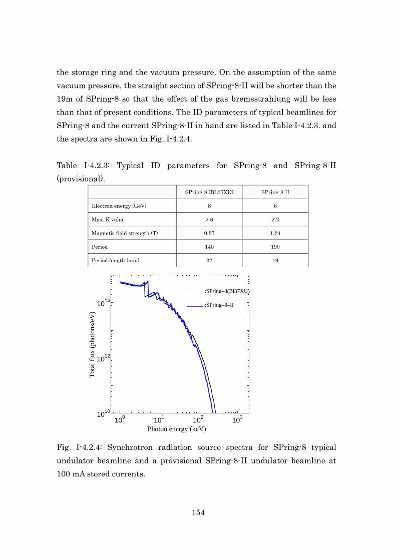
154
the storage ring and the vacuum pressure. On the assumption of the same vacuum pressure, the straight section of SPring-8-II will be shorter than the 19m of SPring-8 so that the effect of the gas bremsstrahlung will be less than that of present conditions. The ID parameters of typical beamlines for SPring-8 and the current SPring-8-II in hand are listed in Table I-4.2.3. and the spectra are shown in Fig. I-4.2.4. Table I-4.2.3: Typical ID parameters for SPring-8 and SPring-8-II (provisional).
SPring-8 (BL37XU) SPring-8-II
Electron energy (GeV) 8 6
Max. K value 2.6 2.2
Magnetic field strength (T) 0.87 1.24
Period 140 190
Period length (mm) 32 19
Fig. I-4.2.4: Synchrotron radiation source spectra for SPring-8 typical undulator beamline and a provisional SPring-8-II undulator beamline at 100 mA stored currents.
100 101 102 1031010
1012
1014
Photon energy (keV)
Tota
l flu
x (p
hoto
ns/e
V)
:SPring–8(Bl37XU)
:SPring–8–II
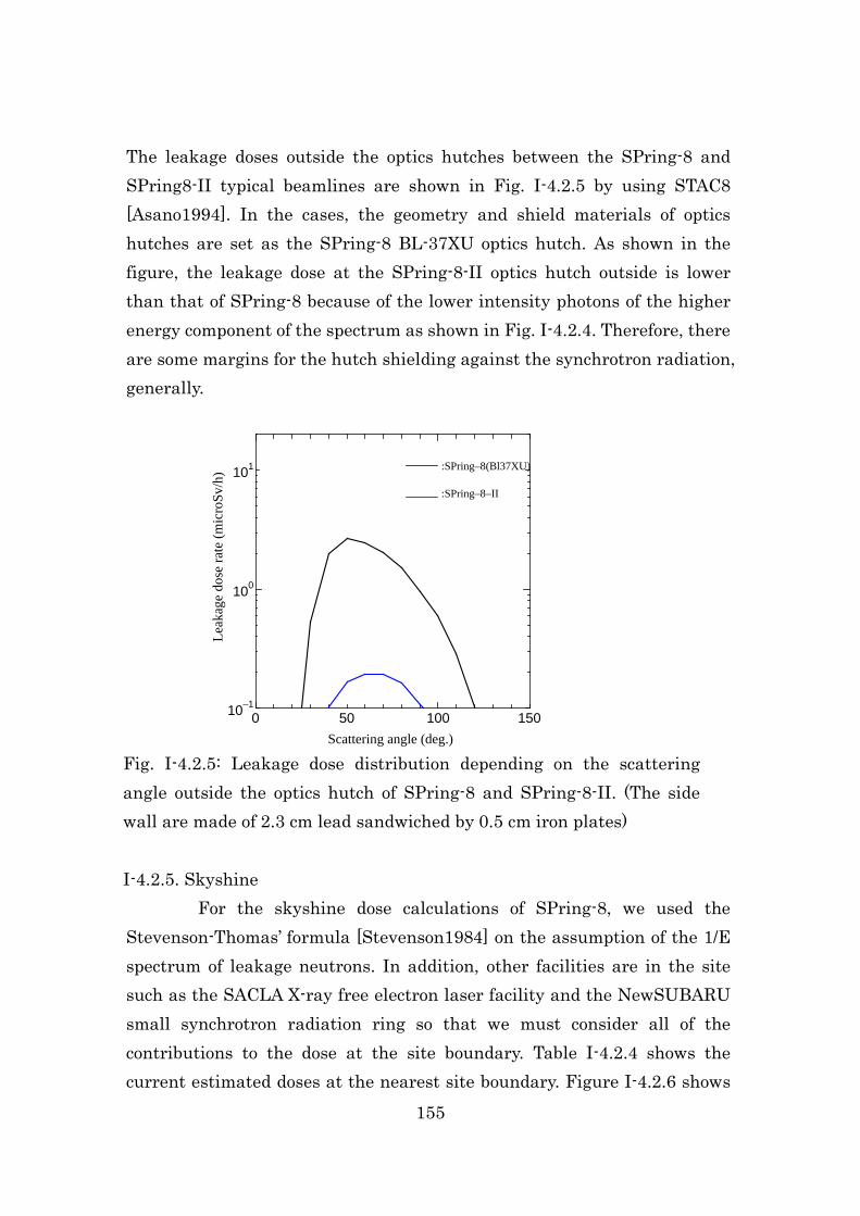
155
The leakage doses outside the optics hutches between the SPring-8 and SPring8-II typical beamlines are shown in Fig. I-4.2.5 by using STAC8 [Asano1994]. In the cases, the geometry and shield materials of optics hutches are set as the SPring-8 BL-37XU optics hutch. As shown in the figure, the leakage dose at the SPring-8-II optics hutch outside is lower than that of SPring-8 because of the lower intensity photons of the higher energy component of the spectrum as shown in Fig. I-4.2.4. Therefore, there are some margins for the hutch shielding against the synchrotron radiation, generally.
Fig. I-4.2.5: Leakage dose distribution depending on the scattering angle outside the optics hutch of SPring-8 and SPring-8-II. (The side wall are made of 2.3 cm lead sandwiched by 0.5 cm iron plates)
I-4.2.5. Skyshine
For the skyshine dose calculations of SPring-8, we used the Stevenson-Thomas’ formula [Stevenson1984] on the assumption of the 1/E spectrum of leakage neutrons. In addition, other facilities are in the site such as the SACLA X-ray free electron laser facility and the NewSUBARU small synchrotron radiation ring so that we must consider all of the contributions to the dose at the site boundary. Table I-4.2.4 shows the current estimated doses at the nearest site boundary. Figure I-4.2.6 shows
0 50 100 15010–1
100
101
Scattering angle (deg.)
Leak
age
dose
rate
(mic
roSv
/h) :SPring–8(Bl37XU)
:SPring–8–II
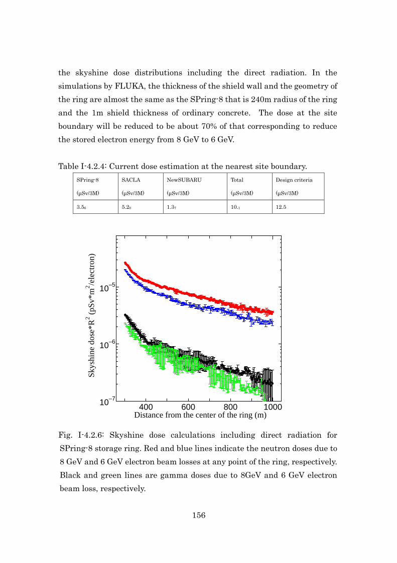
156
the skyshine dose distributions including the direct radiation. In the simulations by FLUKA, the thickness of the shield wall and the geometry of the ring are almost the same as the SPring-8 that is 240m radius of the ring and the 1m shield thickness of ordinary concrete. The dose at the site boundary will be reduced to be about 70% of that corresponding to reduce the stored electron energy from 8 GeV to 6 GeV.
Table I-4.2.4: Current dose estimation at the nearest site boundary.
SPring-8
(μSv/3M)
SACLA
(μSv/3M)
NewSUBARU
(μSv/3M)
Total
(μSv/3M)
Design criteria
(μSv/3M)
3.56 5.20 1.37 10.1 12.5
Fig. I-4.2.6: Skyshine dose calculations including direct radiation for SPring-8 storage ring. Red and blue lines indicate the neutron doses due to 8 GeV and 6 GeV electron beam losses at any point of the ring, respectively. Black and green lines are gamma doses due to 8GeV and 6 GeV electron beam loss, respectively.
400 600 800 100010–7
10–6
10–5
Distance from the center of the ring (m)
Skys
hine
dos
e*R
2 (pSv
*m2 /e
lect
ron)
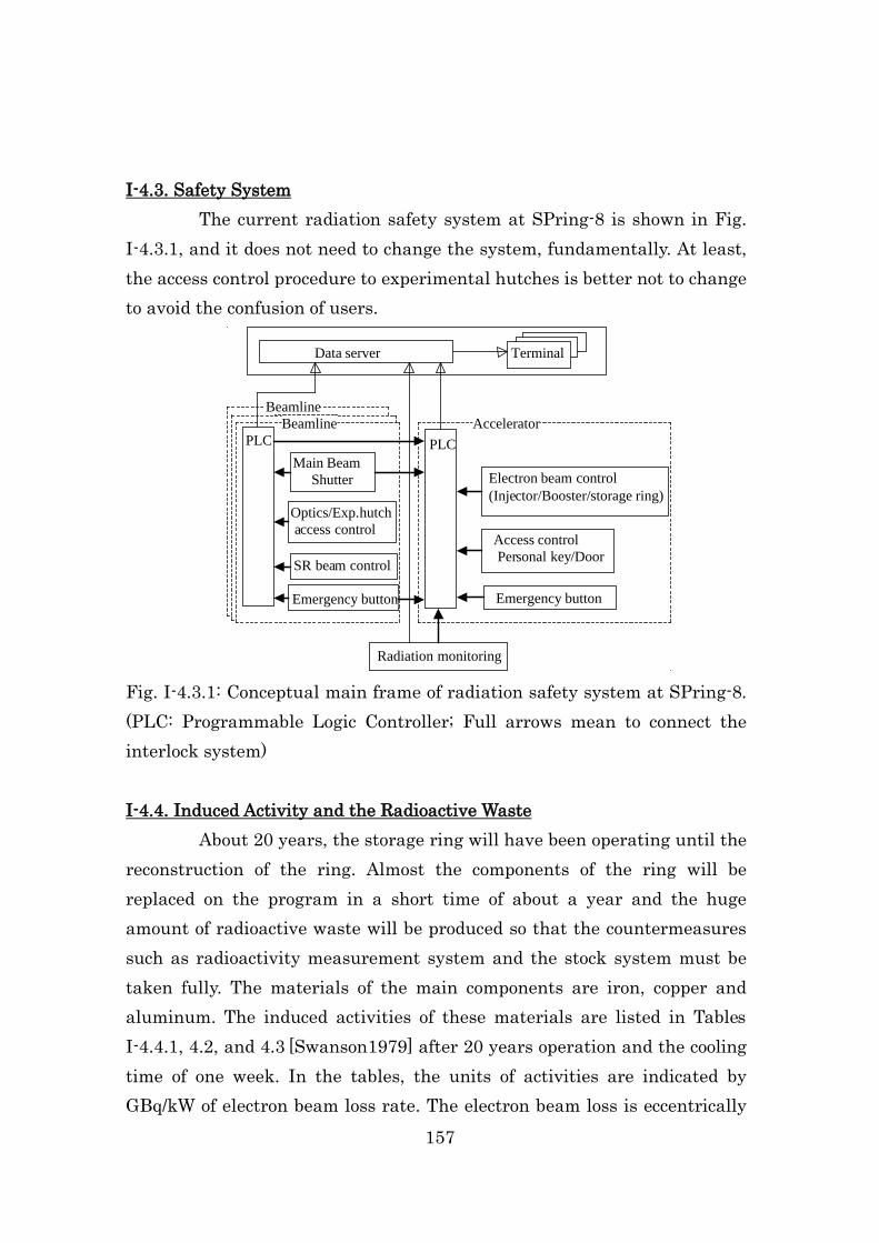
157
I-4.3. Safety System
The current radiation safety system at SPring-8 is shown in Fig. I-4.3.1, and it does not need to change the system, fundamentally. At least, the access control procedure to experimental hutches is better not to change to avoid the confusion of users.
Fig. I-4.3.1: Conceptual main frame of radiation safety system at SPring-8. (PLC: Programmable Logic Controller; Full arrows mean to connect the interlock system)
I-4.4. Induced Activity and the Radioactive Waste
About 20 years, the storage ring will have been operating until the reconstruction of the ring. Almost the components of the ring will be replaced on the program in a short time of about a year and the huge amount of radioactive waste will be produced so that the countermeasures such as radioactivity measurement system and the stock system must be taken fully. The materials of the main components are iron, copper and aluminum. The induced activities of these materials are listed in Tables I-4.4.1, 4.2, and 4.3 [Swanson1979] after 20 years operation and the cooling time of one week. In the tables, the units of activities are indicated by GBq/kW of electron beam loss rate. The electron beam loss is eccentrically
Beamline
Data server
Beamline
Main Beam Shutter
Optics/Exp.hutch access control
SR beam control
AcceleratorPLC PLC
Electron beam control (Injector/Booster/storage ring)
Access control Personal key/Door
Emergency button Emergency button
Radiation monitoring
Terminal
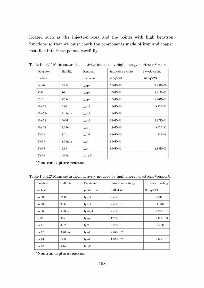
158
located such as the injection area and the points with high betatron functions so that we must check the components made of iron and copper installed into these points, carefully. Table I-4.4.1: Main saturation activity induced by high energy electrons (iron).
Daughter
nuclide
Half life Dominant
production
Saturation activity
(GBq/kW)
1 week cooling
(GBq/kW)
Sc-46 83.9d (γ,sp) 7.40E+00 6.98E+00
V-48 16d (γ,sp) 1.50E+01 1.11E+01
Cr-51 27.8d (γ,sp) 1.50E+01 1.26E+01
Mn-52 5.6d (γ,np) 1.30E+00 5.47E-01
Mn-52m 21.1min (γ,np) 1.30E+00 -
Mn-54 303d (γ,np) 2.20E+01 2.17E+01
Mn-56 2.576h (γ,p) 1.20E+00 8.67E-43
Fe-52 8.2h (γ,2n) 2.10E+00 1.43E-06
Fe-53 8.51min (γ,n) 2.70E+01 -
Fe-55 2.6a (γ,n) 4.90E+02 4.85E+02
Fe-59 45.6d (n, γ)* - -
*Neutron capture reaction
Table I-4.4.2: Main saturation activity induced by high energy electrons (copper). Daughter
nuclide
Half life Dominant
production
Saturation activity
(GBq/kW)
1 week cooling
(GBq/kW)
Co-58 71.3d (γ,sp) 2.40E+01 2.24E+01
Co-58m 9.2h (γ,sp) 2.40E+01 1.88E-01
Co-60 5.263a (γ,n2p) 2.40E+01 2.22E+01
Ni-63 92a (γ,np) 1.70E+01 2.38E+00
Cu-61 3.32h (γ,2n) 3.20E+01 8.41E-01
Cu-62 9.76min (γ,n) 4.07E+02 -
Cu-64 12.8h (γ,n) 1.85E+02 9.86E+01
Cu-66 5.1min (n,γ)* - -
*Neutron capture reaction
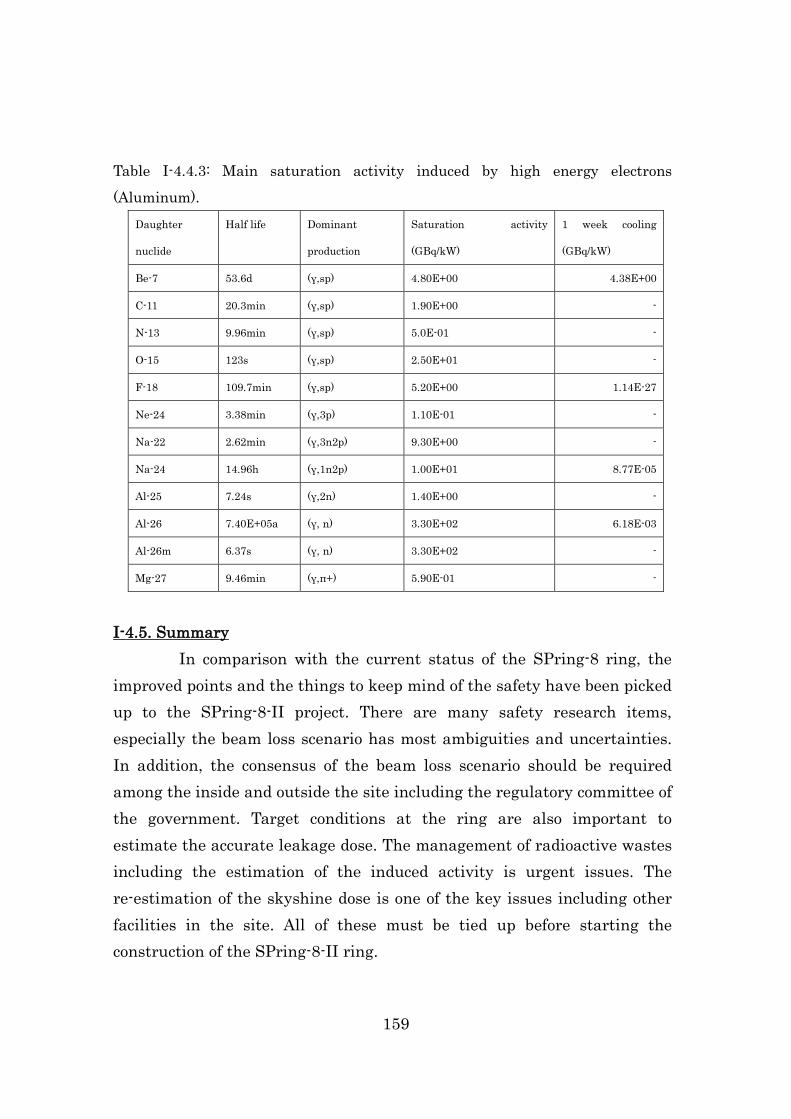
159
Table I-4.4.3: Main saturation activity induced by high energy electrons (Aluminum).
Daughter
nuclide
Half life Dominant
production
Saturation activity
(GBq/kW)
1 week cooling
(GBq/kW)
Be-7 53.6d (γ,sp) 4.80E+00 4.38E+00
C-11 20.3min (γ,sp) 1.90E+00 -
N-13 9.96min (γ,sp) 5.0E-01 -
O-15 123s (γ,sp) 2.50E+01 -
F-18 109.7min (γ,sp) 5.20E+00 1.14E-27
Ne-24 3.38min (γ,3p) 1.10E-01 -
Na-22 2.62min (γ,3n2p) 9.30E+00 -
Na-24 14.96h (γ,1n2p) 1.00E+01 8.77E-05
Al-25 7.24s (γ,2n) 1.40E+00 -
Al-26 7.40E+05a (γ, n) 3.30E+02 6.18E-03
Al-26m 6.37s (γ, n) 3.30E+02 -
Mg-27 9.46min (γ,π+) 5.90E-01 -
I-4.5. Summary
In comparison with the current status of the SPring-8 ring, the improved points and the things to keep mind of the safety have been picked up to the SPring-8-II project. There are many safety research items, especially the beam loss scenario has most ambiguities and uncertainties. In addition, the consensus of the beam loss scenario should be required among the inside and outside the site including the regulatory committee of the government. Target conditions at the ring are also important to estimate the accurate leakage dose. The management of radioactive wastes including the estimation of the induced activity is urgent issues. The re-estimation of the skyshine dose is one of the key issues including other facilities in the site. All of these must be tied up before starting the construction of the SPring-8-II ring.

160
References [Asano1994] Y.Asano & N.Sasamoto,, Radiation Physics and Chemistry Vol.44 No1/2 p.133-137 (1994). [Asano2007] Yoshihiro Asano & Tetsuya Takagi, Radiation measurements Vol.41 p.s236-241 (2007). [Asano2013] Yoshihiro Asano, J. Radiation Protection & Environments Vol.35 p.135-144 (2013). ISSN 0972-0464 [Fasso2005] A. Fasso et al., CERN-2005-10(2005); A. Fasso et al.,IFFN/TC_5/11; A. Fasso et al., SLAC-Report-773. [Jenkins1979] T. M. Jenkins, Nuclear Instr. & Methods Vol.159 p.265-288 (1979). [Nelson1985] W. R. Nelson, H. Hirayama and D. W. O. Rogers, SLAC-Report 265 (1985). [Nelson2005] W. R. Nelson & T. M. Jenkins, SLAC-Report 737 (2005). [Sasamoto1994] N. Sasamoto and Y. Asano, Proceedings of the 1st specialist's meeting on Shielding aspects of Accelerators, Targets and Irradiation Facilities: SATIF 1994 OECD NEA Documents p.235-245 (1994). [Stevenson1984] G. H. Stevenson & R. H. Thomas, Health Physics Vol.46 No.1 p.115-122(1984). [Swanson1979] W. P. Swanson, IAEA Technical Reports No.188 (1979). [Tanaka2004] H. Tanaka et al., Proceedings of 9th European Particle Accelerator Conference, p.222-224 Lucerne, Swiss (2004).

161
PART-II II-1 Overview
162
II-1. Overview Over the last half century, synchrotron radiation (SR) light sources
have steadily evolved with significant increases in brilliance. The advent of 3rd generation synchrotron facilities (e.g., ESRF, APS, and SPring-8 in the 1990s) together with the emergence of new experimental techniques drastically expanded the ranges for applications. These facilities, as well as subsequent medium-sized light sources, are now regarded as vital scientific infrastructure required to address essential problems facing society today.
A recent remarkable milestone in optical science is the development of XFEL light sources. At SPring-8, we inaugurated SACLA, the first compact XFEL facility, in 2012. SACLA produces ultrabrilliant, femtosecond X-ray pulses with excellent transverse coherence. These characteristics are completely different from those of SR sources that have modest peak intensity with quasi-CW pulse patterns. A new scheme, “measurement-before-destruction” (MBD), has been exploited as a key concept for experiments using XFEL. This technique offers atomic-scale spatial information with femtosecond snapshots, while the destructive property requires a huge number of repetitive measurements in order to understand the whole processes. This scheme is thus suited for elucidating fundamental characteristics using many replica samples, rather than for tracing spatiotemporal correlations and evolutions for a single complex target. For the latter purpose, SR is still an indispensable X-ray probe. The wide gap between XFEL and SR, however, has recently been recognized as a serious challenge that must be overcome in order to reveal the fundamental nature of materials of interest.
Our upgrade plan for the SPring-8 facility calls for bridging this gap by making drastic enhancements to SR capabilities. A brighter SR source naturally allows us to access (i) very complex and minute targets (ii) working in real environments (iii) with improved resolution (iv) using combinative experimental techniques. Moreover, the intense, high repetition-rate source enables (v) drastic reduction of the time constant of measurement from seconds to the millisecond or even microsecond range for

163
a broad range of applications. Based on these advanced capabilities, we plan to build a new scheme, “measurement-during-change”, as a standard experimental concept for SPring-8-II, which is distinct from the “static” observation available in the existing SPring-8 beamlines or from the MBD scheme used at SACLA. Practical utilization of X-ray nanoscopy combined with diffraction/scattering/spectroscopic techniques will enable us to reveal the complex functions of heterogeneous systems in catalytic and energy materials, to illuminate fluctuating dynamics in strongly correlated systems, to clarify distinct the characteristics of matter in extreme conditions, and to investigate essential reactions among biomolecules. Understanding these fundamental questions will provide promising clues on improving sustainability, major progress in information technology, management of disaster, and control & prevention of diseases. Several interesting scientific cases for ultralow-emittance SR sources proposed at the present stage can be found in the special issue “Diffraction-Limited Storage Rings and New Science Opportunities” in the Journal of Synchrotron Radiation [JSR2014].
To realize the potential of the upgraded facility, we must fully exploit the capabilities of the SPring-8-II light source. This necessitates upgrading the whole experimental system, including the beamlines, the end-stations, and the detector system [Yabashi2014].
For the beamlines, a primary challenge at the start of SPring-8 was how to manage high heat loads above 400 W for the most upstream optics. For SPring-8-II, the heat load will be mitigated, as described in Part I. A key requirement for SPring-8-II is speckle-free properties for all optics, including mirrors, crystals, and windows, to preserve coherent X-ray wavefronts. Another mandate is to reduce instability. To generate a small focusing spot using a current SPring-8 beamline, one utilizes a secondary slit as a virtual source, which removes an unwanted influence of instability, originating mainly from a double-crystal monochromator (DCM). However, this geometry results in the loss of considerable amounts of available photon flux for the samples. If we could remove the secondary slit at SPring-8-II, we would be able to keep the flux of ~1014 photons/s from the
164
source within an ultra-small spot of ~150×230 nm2. The flux density in this focusing condition is three orders of magnitude higher than that in the existing SPring-8 beamline. To achieve stabilization, it is increasing important to damp vibration of the cooling system, as well as to utilize precise X-ray diagnostics. Beamline design is described in more detail in Sect. II-2.
For end-stations, precise and fast data acquisition is essential for efficient utilization of SPring-8-II. This requires a detailed synchronization scheme among motions of sample stages, operand parameters, detectors, and data analysis. However, the technological development needed to meet the requirements is massive. Thus, core systems, which are extracted from various types of experimental setups, should be designed and constructed in a centralized and standardized way. Applications for each experimental instrument are conducted as variants of the core systems. This strategy is in contrast to that performed at end-stations of the existing SPring-8 facility, where development of experimental instruments is conducted rather independently at each place. Since the design work of the core systems is still in a very early stage, we do not include a detailed description in this report. However, in Sect. II-3 we present a design strategy for the detector system, which is the most important component of the core systems.
To reach this goal, we are able to exploit the experience gained and resources developed for SACLA utilization. At SACLA beamlines, state-of-the-art X-ray optical components are operated for advanced applications such as quantum X-ray optics, coherent diffractive imaging (CDI), and high-energy density science. Non-destructive beam monitors provide X-ray beam parameters in a shot-by-shot manner, allowing users to conduct reliable analysis on experimental data [Tono2013]. In the SACLA end-stations, standardized experimental systems are designed, constructed, and operated to address the majority of user applications. A good example is the DAPHNIS system, which was developed as a diffraction/scattering experimental platform. The system consists of a compact sample chamber, various types of sample injectors, and a short-work-distance octal MPCCD

165
detector [Kameshima2014; Tono2015]. Additionally, the DAQ system was developed for handling and analyzing massive data streams with a rate of ~4 Gbps and a volume of ~10 TB/day. Based on these prototype systems, we intend to design core experimental platforms for synthetic utilization of SPring-8-II.
Finally, we describe possible scenarios of how we intend to carry out the beamline upgrade. We could consider some alternatives depending on the available resources. If we have sufficient resources, we could upgrade all the beamlines and end-stations simultaneously with the accelerator upgrade. In case our resources are rather limited, we will start the upgrade for a select number of beamlines. Even in this case, one could continue to utilize the existing beamlines without major changes, whereas the performance is limited. To maintain compatibility between the existing and upgraded beamlines, we will preserve the beam axes for almost all beamlines, as described in Sect. I, except for realignment of the bending magnet B2 beamlines due to the small changes of the beam axes. This scenario allows us to balance resources over an extended term, rather than concentrating them into a short period. References [JSR2014] Special issue on Diffraction-Limited Storage Rings and New Science Opportunities, J. Synchrotron Rad. 21, Part 5 (2014). [Kameshima2014] T. Kameshima et al., Rev. Sci. Instrum. 85 (2014) 033110. [Tono2013] K. Tono et al., New. J. Phys. 12 (2013) 083035. [Tono2015] K. Tono et al., submitted. [Yabashi2014] M. Yabashi et al., J. Synchrotron Rad. 21 (2014) 976-985.

166
PART-II II-2 Beamline Design
II-2.1. High-heat-load optics II-2.2. X-ray optics with wavefront preservation II-2.3. Photon diagnostics II-2.4. New experimental schemes with innovative optics
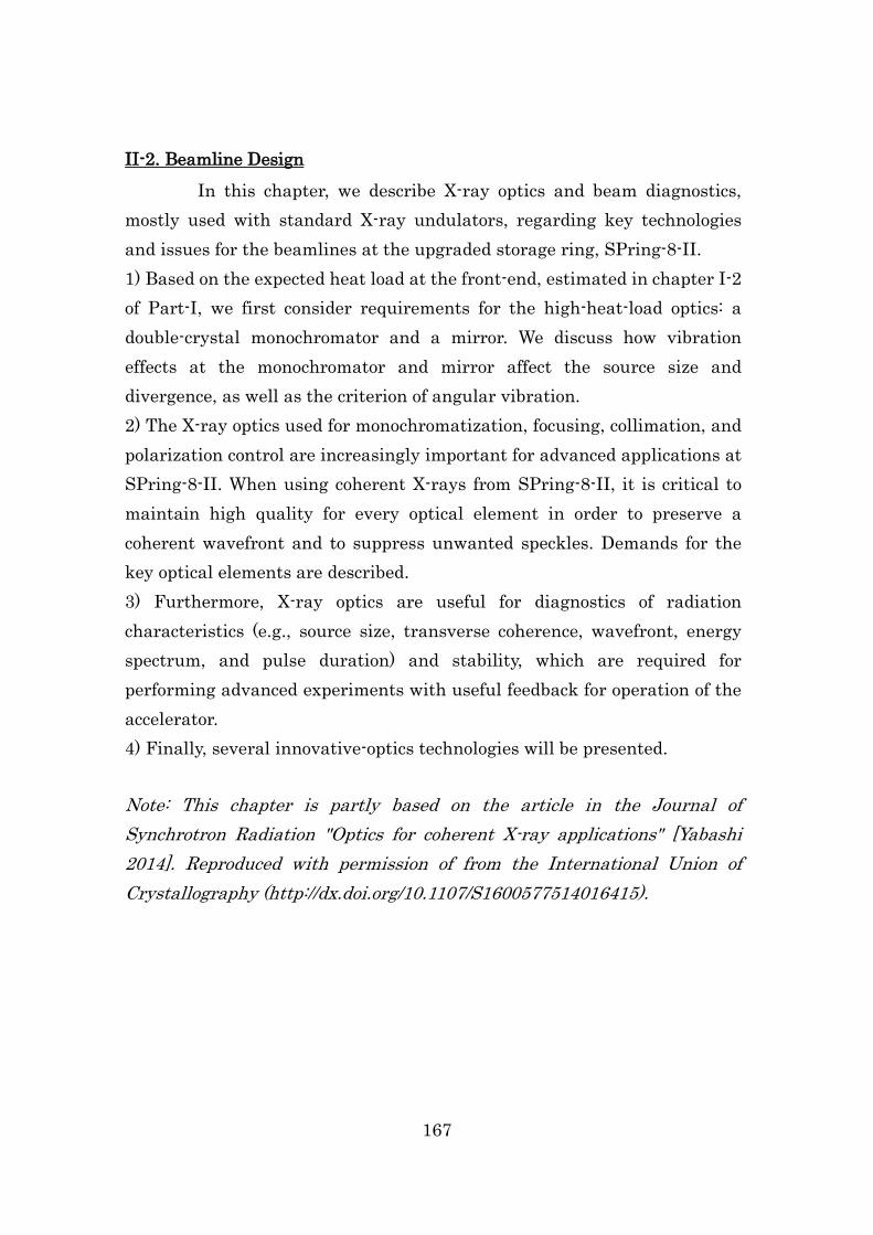
167
II-2. Beamline Design In this chapter, we describe X-ray optics and beam diagnostics,
mostly used with standard X-ray undulators, regarding key technologies and issues for the beamlines at the upgraded storage ring, SPring-8-II. 1) Based on the expected heat load at the front-end, estimated in chapter I-2 of Part-I, we first consider requirements for the high-heat-load optics: a double-crystal monochromator and a mirror. We discuss how vibration effects at the monochromator and mirror affect the source size and divergence, as well as the criterion of angular vibration. 2) The X-ray optics used for monochromatization, focusing, collimation, and polarization control are increasingly important for advanced applications at SPring-8-II. When using coherent X-rays from SPring-8-II, it is critical to maintain high quality for every optical element in order to preserve a coherent wavefront and to suppress unwanted speckles. Demands for the key optical elements are described. 3) Furthermore, X-ray optics are useful for diagnostics of radiation characteristics (e.g., source size, transverse coherence, wavefront, energy spectrum, and pulse duration) and stability, which are required for performing advanced experiments with useful feedback for operation of the accelerator. 4) Finally, several innovative-optics technologies will be presented. Note: This chapter is partly based on the article in the Journal of Synchrotron Radiation "Optics for coherent X-ray applications" [Yabashi 2014]. Reproduced with permission of from the International Union of Crystallography (http://dx.doi.org/10.1107/S1600577514016415).

168
II-2.1. High-heat-load optics II-2.1.1. Double-crystal monochromators (DCMs)
We propose to use short-period in-vacuum undulators (e.g., λu of 22 mm) to produce high photon energies at 6-GeV operation for the standard X-ray undulator beamline. In this case, one can keep the maximum K parameter over 2.3, which continuously covers a wide wavelength range by combining odd harmonics, with a minimum gap of 5 mm. We expect an increase of brilliance by a factor of 20 (Fig. II-2.1.1). Figures II-2.1.2 (a) and (b) show the comparison of the beam profiles of the central cone of the fundamental peaks observed at 30 m from the source. The horizontal beam size for the new design is more concentrated due to the smaller horizontal emittance. The vertical beam size is slightly larger due to the shorter length of the undulator. The smaller horizontal emittance helps to reduce the heat load on the first optical element, because one can control the aperture size of a pre-slit for the first optics without losing photon flux with moderate power. In the case of SPring-8-II, an aperture size of 1.1 mm(H) × 0.97 mm(V) for the frontend pre-slit is large enough to accommodate the central cone of the X-ray beam, which suppresses the maximum heat load below 300 W at a stored current of 100 mA. This is a typical amount of power, which is sufficiently controlled at the existing SPring-8 beamlines. Thus we could adopt the same cooling scheme for the first crystal of DCMs at SPring-8-II: indirect cooling using liquid nitrogen (LN2) circulation. In order to suppress thermal deformation of the silicon crystals, LN2 cooling has been widely applied for DCMs [Mochizuki 2001]. Figure II-2.1.3 shows the photon flux available using odd harmonics at K= 2.3. The photon flux with a Si 111 double-crystal monochromator (DCM) reaches ~1014 photons/s for a photon energy range below 15 keV, which is ~50% higher than that of the existing SPring-8 beamlines.

169
Fig. II-2.1.1: Increase of brilliance at the standard X-ray undulator at SPring-8-II, compared with that of SPring-8, for 10-keV X-rays with fundamental peaks.
Fig. II-2.1.2: Central cones of the fundamental peaks observed at 30 m from the source at K= 2.3.
(a) SPring-8 (8 GeV, λu= 32 mm, N= 140, I= 100 mA), (b) SPring-8-II (6 GeV, λu= 22 mm, N= 163, I= 100 mA).
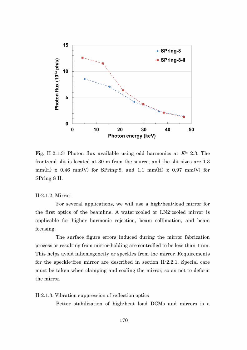
170
Fig. II-2.1.3: Photon flux available using odd harmonics at K= 2.3. The front-end slit is located at 30 m from the source, and the slit sizes are 1.3 mm(H) x 0.46 mm(V) for SPring-8, and 1.1 mm(H) x 0.97 mm(V) for SPring-8-II. II-2.1.2. Mirror
For several applications, we will use a high-heat-load mirror for the first optics of the beamline. A water-cooled or LN2-cooled mirror is applicable for higher harmonic rejection, beam collimation, and beam focusing.
The surface figure errors induced during the mirror fabrication process or resulting from mirror-holding are controlled to be less than 1 nm. This helps avoid inhomogeneity or speckles from the mirror. Requirements for the speckle-free mirror are described in section II-2.2.1. Special care must be taken when clamping and cooling the mirror, so as not to deform the mirror. II-2.1.3. Vibration suppression of reflection optics
Better stabilization of high-heat load DCMs and mirrors is a

171
critical challenge for utilization of SPring-8-II. In the case of LN2 cooling, the bumping of vaporized nitrogen could be a cause of vibration, in addition to typical sources such as the pulsations of coolant pumps and the turbulence within flow channels. To suppress short-term fluctuations (i.e., vibrations), the characteristics of the flexible tubes used for the flow channel are of great importance [Yamazaki 2013]. This is because the corrugation of a flexible tube can easily produce unwanted turbulence in the flow of LN2.
We recently developed a low-vibration flexible tube with low turbulence. A standard flexible tube made of stainless steel is fitted with soft sleeves of alumina fiber to serve as a smooth inner lining. This inner tube can remain pliable at LN2 temperature levels under radiation. Figure II-2.1.4 shows a trend of 12-keV X-ray intensity after the LN2-cooled DCM using (a) standard tubes and (b) the aforementioned low-vibration tubes, measured at an undulator beamline of SPring-8 with a sampling rate of 1 kHz. The angular fluctuation (peak-peak) was reduced from 5 μrad to 0.75 μrad with a corresponding decrease of intensity fluctuation from 5.3% to 2.0%. Even smaller angular fluctuation, however, is needed to reduce the growth of virtual source size and divergence caused by vibration.
Minute vibrations in the reflection optics cause a virtual increase of the source size and divergence [Goto 2014]. Figure II-2.1.5 shows the scheme, indicating how beam size and divergence grow due to vibrations. The virtual source size and divergence will be:
22,
222,2
,2
,vyx
vyxyxyx
zS
′′′
′′′
+Σ
Σ+Σ=
σσ
, (II-2.1.1)
22,
2, vyxyxS ′′′′′ +Σ= σ , (II-2.1.2)
where, z : the distance between the source and reflection optics, yx,Σ : the source size (convolution of electron and photon size), yx ′′Σ , : the source divergence (convolution of electron and photon divergence), and v′σ : the effective (rms) angular vibration of the reflected beam due to angular

172
vibration of the optics. v′σ is twice the angular vibration of the optics such as total reflection mirror and symmetrical-Bragg-case diffraction of perfect crystals. We assume that v′σ is very small, so that the reflectivity is maintained. In addition to increasing the effective beam size at the downstream location, the virtual beam waist shifts along the optical axis. The distance between the virtual beam waist and the reflection optics becomes:
zvyx
yx22
,
2,
′′′
′′
+Σ
Σ=
σς . (II-2.1.3)
The beam size observed with non-focusing optics will be expressed by convolution of the intrinsic beam size and the contribution of vibration:
( )2222',
2, zLLS vyxyxL −+Σ+Σ= ′′ σ (II-2.1.4)
where, L is the distance from the source, 22',
2, Lyxyx ′Σ+Σ provides the
intrinsic beam size, and ( )zLv −′σ is the contribution of vibration.
Using these equations, we can evaluate the criterion of vibration suppression, compared with the source size and divergence, particularly in the vertical direction. We must suppress the angular vibration as
yvxv ′′′′ Σ<<Σ<< σσ or . For example, we consider a vibration effect for DCM located at 40 m from the vertical beam size by eq. II-2.1.1. A 10% increase in the vertical size (in the case of μm6=Σ y , μrad2.4=Σ ′y , and μm6.6=yS ) corresponds to μrad07.0=′vσ . This is 1/10~1/5 of the present value. Thus, vibration suppression becomes more critical.
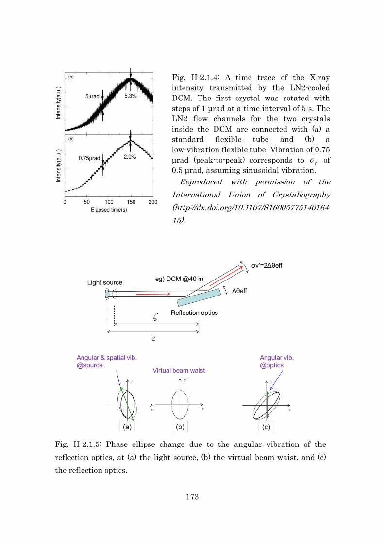
173
Fig. II-2.1.5: Phase ellipse change due to the angular vibration of the reflection optics, at (a) the light source, (b) the virtual beam waist, and (c) the reflection optics.
Fig. II-2.1.4: A time trace of the X-ray intensity transmitted by the LN2-cooled DCM. The first crystal was rotated with steps of 1 μrad at a time interval of 5 s. The LN2 flow channels for the two crystals inside the DCM are connected with (a) a standard flexible tube and (b) a low-vibration flexible tube. Vibration of 0.75 μrad (peak-to-peak) corresponds to v′σ of 0.5 μrad, assuming sinusoidal vibration. Reproduced with permission of the International Union of Crystallography (http://dx.doi.org/10.1107/S1600577514016415).
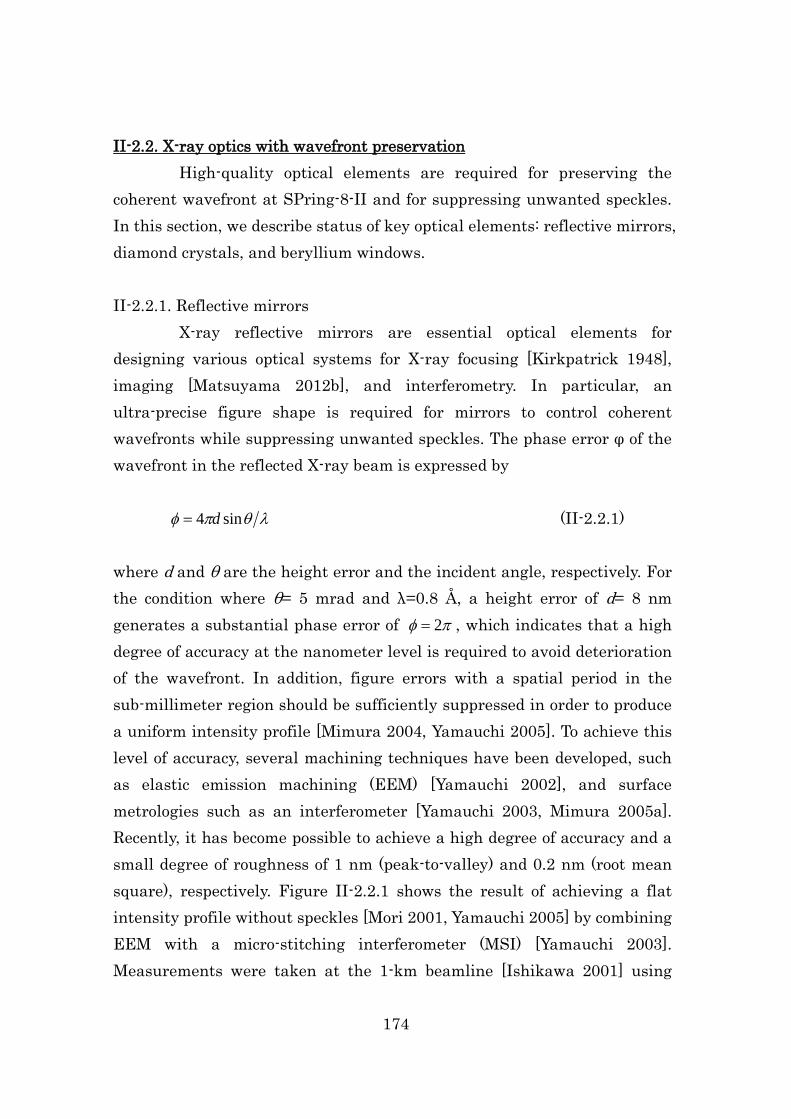
174
II-2.2. X-ray optics with wavefront preservation High-quality optical elements are required for preserving the
coherent wavefront at SPring-8-II and for suppressing unwanted speckles. In this section, we describe status of key optical elements: reflective mirrors, diamond crystals, and beryllium windows. II-2.2.1. Reflective mirrors
X-ray reflective mirrors are essential optical elements for designing various optical systems for X-ray focusing [Kirkpatrick 1948], imaging [Matsuyama 2012b], and interferometry. In particular, an ultra-precise figure shape is required for mirrors to control coherent wavefronts while suppressing unwanted speckles. The phase error φ of the wavefront in the reflected X-ray beam is expressed by
λθπφ sin4 d= (II-2.2.1) where d and θ are the height error and the incident angle, respectively. For the condition where θ= 5 mrad and λ=0.8 Å, a height error of d= 8 nm generates a substantial phase error of πφ 2= , which indicates that a high degree of accuracy at the nanometer level is required to avoid deterioration of the wavefront. In addition, figure errors with a spatial period in the sub-millimeter region should be sufficiently suppressed in order to produce a uniform intensity profile [Mimura 2004, Yamauchi 2005]. To achieve this level of accuracy, several machining techniques have been developed, such as elastic emission machining (EEM) [Yamauchi 2002], and surface metrologies such as an interferometer [Yamauchi 2003, Mimura 2005a]. Recently, it has become possible to achieve a high degree of accuracy and a small degree of roughness of 1 nm (peak-to-valley) and 0.2 nm (root mean square), respectively. Figure II-2.2.1 shows the result of achieving a flat intensity profile without speckles [Mori 2001, Yamauchi 2005] by combining EEM with a micro-stitching interferometer (MSI) [Yamauchi 2003]. Measurements were taken at the 1-km beamline [Ishikawa 2001] using
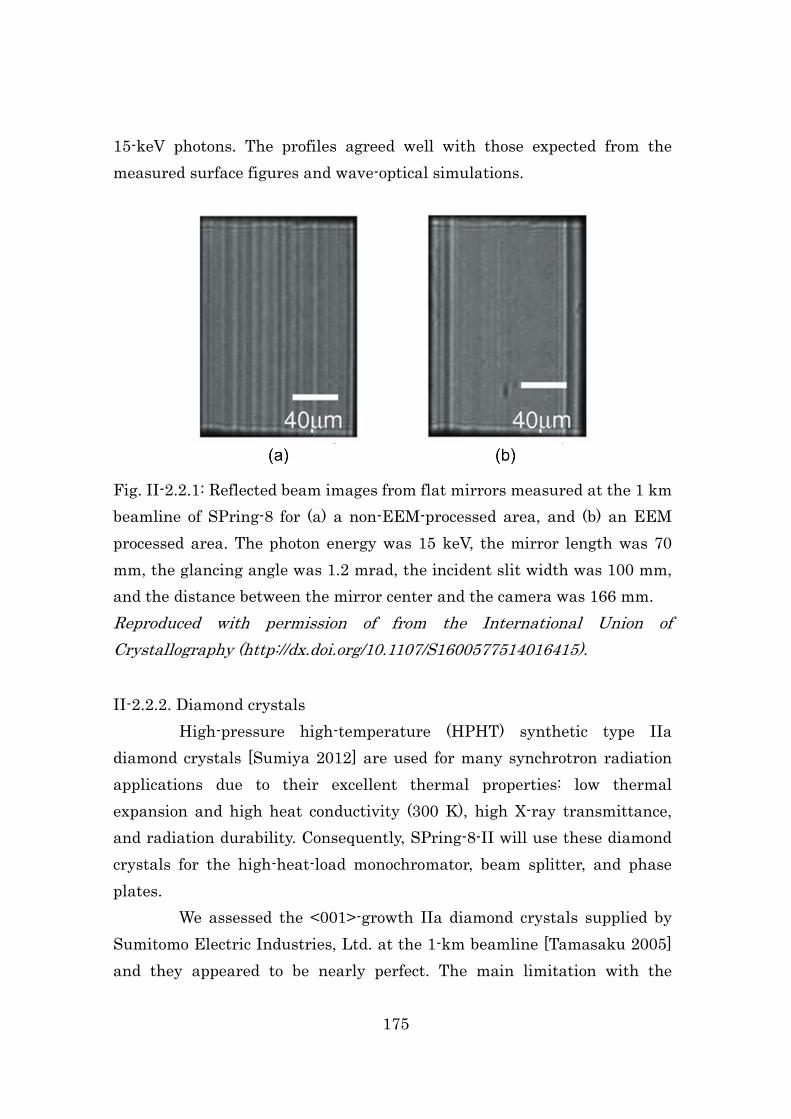
175
15-keV photons. The profiles agreed well with those expected from the measured surface figures and wave-optical simulations.
Fig. II-2.2.1: Reflected beam images from flat mirrors measured at the 1 km beamline of SPring-8 for (a) a non-EEM-processed area, and (b) an EEM processed area. The photon energy was 15 keV, the mirror length was 70 mm, the glancing angle was 1.2 mrad, the incident slit width was 100 mm, and the distance between the mirror center and the camera was 166 mm. Reproduced with permission of from the International Union of Crystallography (http://dx.doi.org/10.1107/S1600577514016415). II-2.2.2. Diamond crystals
High-pressure high-temperature (HPHT) synthetic type IIa diamond crystals [Sumiya 2012] are used for many synchrotron radiation applications due to their excellent thermal properties: low thermal expansion and high heat conductivity (300 K), high X-ray transmittance, and radiation durability. Consequently, SPring-8-II will use these diamond crystals for the high-heat-load monochromator, beam splitter, and phase plates.
We assessed the <001>-growth IIa diamond crystals supplied by Sumitomo Electric Industries, Ltd. at the 1-km beamline [Tamasaku 2005] and they appeared to be nearly perfect. The main limitation with the

176
diamond crystals was the non-uniformity of the intensity profiles of the reflected beam that was enhanced at the experimental station, located at a distance over 10 m from the monochromator when they were used for the double-crystal monochromator [Yabashi 2007]. A beam profile with speckles presents serious problems for coherent X-ray applications. A non-uniform profile with fringes up to 50% (rms) was observed in the X-ray beam images from the double-crystal monochromator at BL39XU at SPring-8. We performed simple simulations based on Fresnel diffraction from crystal segments, divided by the growth sector boundaries. When we assumed phase shifts due to a lattice inclination of 0.5 μrad or more, or a lattice step due to stacking faults, it caused a similar non-uniformity in the experimental results [Goto 2012]. The simple model suggests that a smaller phase shift in the whole region in the crystal is essential for wavefront preservation. Diamond crystals with better quality and a larger domain are required for practical use at the SPring-8-II facility. II-2.2.3. X-ray windows
Beryllium foil will be used for vacuum windows at the hard X-ray beamlines at SPring-8-II. The transmission of X-rays requires that the windows have high quality, without any speckles or non-uniformity.
After systematic studies, we found that speckles with bright spots resulted from internal voids, which were several to dozens of microns in diameter, for conventional beryllium foils fabricated by powder sintering (Electrofusion, PF-60) and a high-purity ingot foil (Electrofusion, IF-1) [Goto 2004]. A beryllium foil fabricated using physical-vapour-deposition (PVD) has fewer or even no internal voids [Goto 2007]. Figure II-2.2.2 shows the transmission X-ray images for PF-60, IF-1, and PVD beryllium foils measured at the 1-km beamline with a wavelength of 0.1 nm. They were supplied by the Electrofusion and polished to 0.1 μm (rms) or less. A two-dimensional X-ray detector with a spatial resolution of 0.5 μm was used for the observation. The sample-detector distance was set to 1.4 m. Fig. II-2.2.2 (d) shows the Fresnel diffraction patterns calculated for spherical
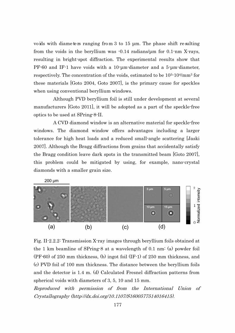
177
vo ids with diame te rs ranging fro m 3 to 15 μm. The phase shift re sulting from the voids in the beryllium was -0.14 radians/μm for 0.1-nm X-rays, resulting in bright-spot diffraction. The experimental results show that PF-60 and IF-1 have voids with a 10-μm-diameter and a 5-μm-diameter, respectively. The concentration of the voids, estimated to be 103-104/mm3 for these materials [Goto 2004, Goto 2007], is the primary cause for speckles when using conventional beryllium windows.
Although PVD beryllium foil is still under development at several manufacturers [Goto 2011], it will be adopted as a part of the speckle-free optics to be used at SPring-8-II.
A CVD diamond window is an alternative material for speckle-free windows. The diamond window offers advantages including a larger tolerance for high heat loads and a reduced small-angle scattering [Jaski 2007]. Although the Bragg diffractions from grains that accidentally satisfy the Bragg condition leave dark spots in the transmitted beam [Goto 2007], this problem could be mitigated by using, for example, nano-crystal diamonds with a smaller grain size.
Fig. II-2.2.2: Transmission X-ray images through beryllium foils obtained at the 1 km beamline of SPring-8 at a wavelength of 0.1 nm: (a) powder foil (PF-60) of 250 mm thickness, (b) ingot foil (IF-1) of 250 mm thickness, and (c) PVD foil of 100 mm thickness. The distance between the beryllium foils and the detector is 1.4 m. (d) Calculated Fresnel diffraction patterns from spherical voids with diameters of 3, 5, 10 and 15 mm. Reproduced with permission of from the International Union of Crystallography (http://dx.doi.org/10.1107/S1600577514016415).

178
II-2.3. Photon diagnostics SPring-8-II is capable of generating a small intense spot with a
diameter of ~100 nm and a photon flux of more than 1013 photons/s by direct demagnification of the source. Achieving this capability requires high stability for the source and every optical element, particularly in the reflection geometry, because one has to retract the aperture as the secondary source. The target level is less than 0.1 μrad in both the vertical and horizontal directions (see II-2.1.3).
An important step is performing precise diagnostics of the beam properties. We present useful online diagnostics tools and diagnostics of higher-order coherence with Hanbury-Brown and Twiss experiments in the X-ray region, which can provide access to ideal transverse coherence profiles and source sizes, even under conditions of optical instability. II-2.3.1. Online diagnostics
Online photon diagnostics are a prerequisite for new light sources, not only for experiments but also for the stable operation of accelerators and beamlines. In many cases, only a small fraction of X-rays are sampled for diagnostics through interactions between a transparent material and the X-rays. Such materials must have the “speckle-free” quality for wavefront preservation, as scientific applications intended for SPring-8-II rely on a high coherent flux, e.g., coherent X-ray imaging and X-ray photon correlation spectroscopy. For the in-line photon diagnostic systems at SPring-8-II, some good candidates are found in the XFEL beamlines, which also require the preservation of coherent wavefronts. In-line intensity and profile diagnostics have already been in operation at SACLA [Ishikawa 2012, Tono 2013].
One example is an in-line intensity/position monitor, in which scattered X-rays from a thin foil are detected using quadrant photodiodes as shown in Fig. II-2.3.1(a) [Alkire 2000, Tono 2011]. The foil, only 15 μm thick, is composed of small diamond crystals with an average grain size of only a few dozen nanometers. The beam position is obtained from the
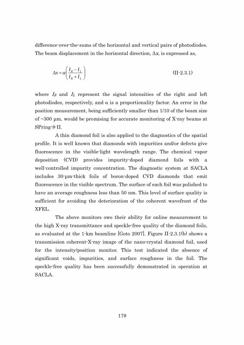
179
difference-over-the-sums of the horizontal and vertical pairs of photodiodes. The beam displacement in the horizontal direction, Δx, is expressed as,
+−
=∆LR
LR
IIIIx α (II-2.3.1)
where IR and IL represent the signal intensities of the right and left photodiodes, respectively, and α is a proportionality factor. An error in the position measurement, being sufficiently smaller than 1/10 of the beam size of ~300 μm, would be promising for accurate monitoring of X-ray beams at SPring-8-II.
A thin diamond foil is also applied to the diagnostics of the spatial profile. It is well known that diamonds with impurities and/or defects give fluorescence in the visible-light wavelength range. The chemical vapor deposition (CVD) provides impurity-doped diamond foils with a well-controlled impurity concentration. The diagnostic system at SACLA includes 30-μm-thick foils of boron-doped CVD diamonds that emit fluorescence in the visible spectrum. The surface of each foil was polished to have an average roughness less than 50 nm. This level of surface quality is sufficient for avoiding the deterioration of the coherent wavefront of the XFEL.
The above monitors owe their ability for online measurement to the high X-ray transmittance and speckle-free quality of the diamond foils, as evaluated at the 1-km beamline [Goto 2007]. Figure II-2.3.1(b) shows a transmission coherent-X-ray image of the nano-crystal diamond foil, used for the intensity/position monitor. This test indicated the absence of significant voids, impurities, and surface roughness in the foil. The speckle-free quality has been successfully demonstrated in operation at SACLA.
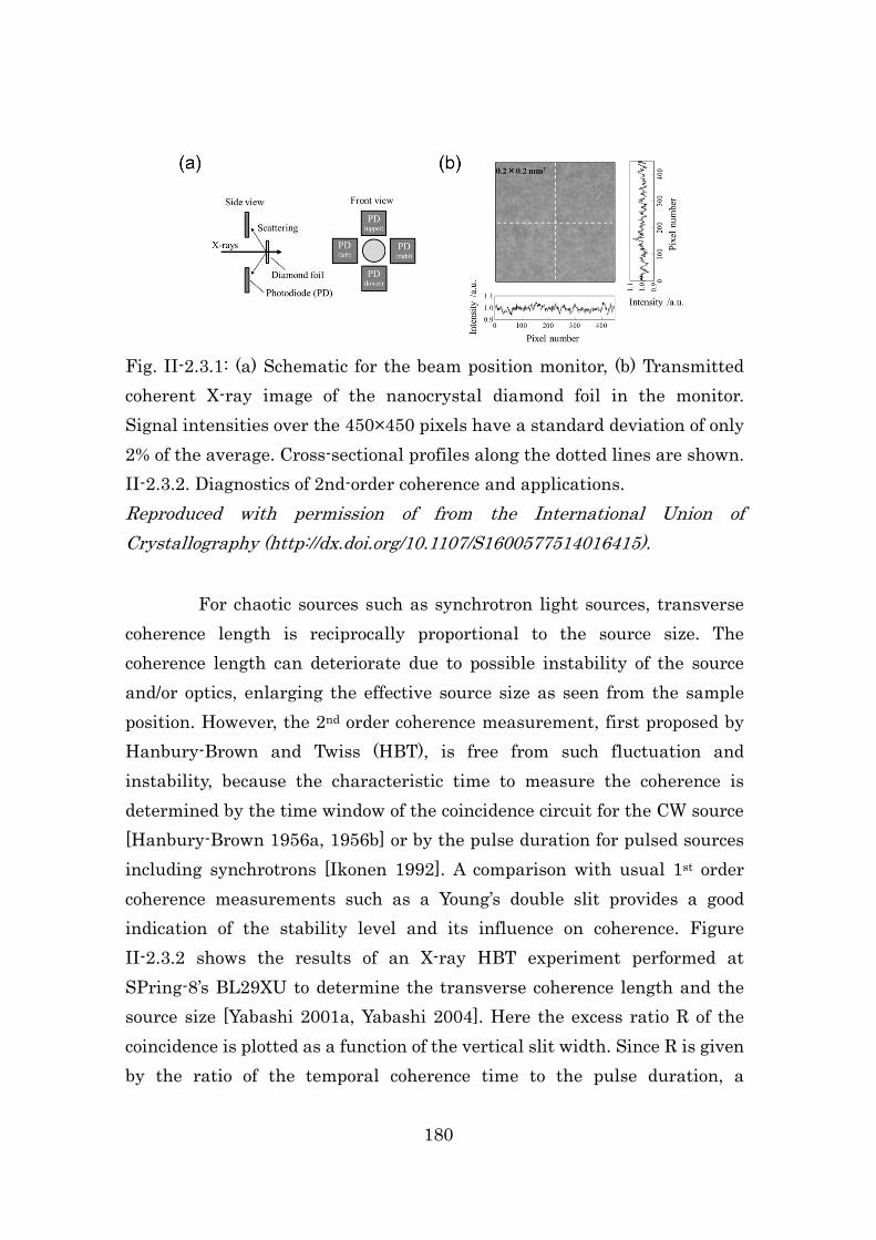
180
Fig. II-2.3.1: (a) Schematic for the beam position monitor, (b) Transmitted coherent X-ray image of the nanocrystal diamond foil in the monitor. Signal intensities over the 450×450 pixels have a standard deviation of only 2% of the average. Cross-sectional profiles along the dotted lines are shown. II-2.3.2. Diagnostics of 2nd-order coherence and applications. Reproduced with permission of from the International Union of Crystallography (http://dx.doi.org/10.1107/S1600577514016415).
For chaotic sources such as synchrotron light sources, transverse coherence length is reciprocally proportional to the source size. The coherence length can deteriorate due to possible instability of the source and/or optics, enlarging the effective source size as seen from the sample position. However, the 2nd order coherence measurement, first proposed by Hanbury-Brown and Twiss (HBT), is free from such fluctuation and instability, because the characteristic time to measure the coherence is determined by the time window of the coincidence circuit for the CW source [Hanbury-Brown 1956a, 1956b] or by the pulse duration for pulsed sources including synchrotrons [Ikonen 1992]. A comparison with usual 1st order coherence measurements such as a Young’s double slit provides a good indication of the stability level and its influence on coherence. Figure II-2.3.2 shows the results of an X-ray HBT experiment performed at SPring-8’s BL29XU to determine the transverse coherence length and the source size [Yabashi 2001a, Yabashi 2004]. Here the excess ratio R of the coincidence is plotted as a function of the vertical slit width. Since R is given by the ratio of the temporal coherence time to the pulse duration, a
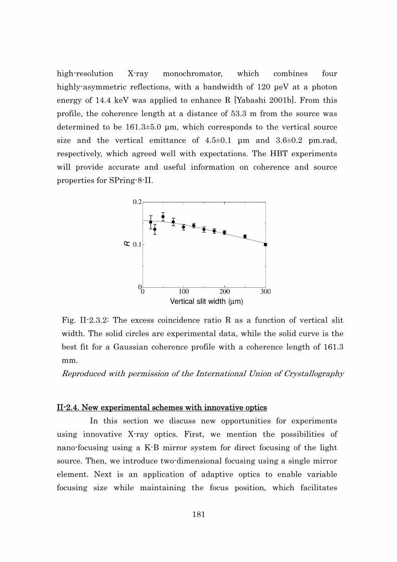
181
high-resolution X-ray monochromator, which combines four highly-asymmetric reflections, with a bandwidth of 120 μeV at a photon energy of 14.4 keV was applied to enhance R [Yabashi 2001b]. From this profile, the coherence length at a distance of 53.3 m from the source was determined to be 161.3±5.0 μm, which corresponds to the vertical source size and the vertical emittance of 4.5±0.1 μm and 3.6±0.2 pm.rad, respectively, which agreed well with expectations. The HBT experiments will provide accurate and useful information on coherence and source properties for SPring-8-II.
II-2.4. New experimental schemes with innovative optics
In this section we discuss new opportunities for experiments using innovative X-ray optics. First, we mention the possibilities of nano-focusing using a K-B mirror system for direct focusing of the light source. Then, we introduce two-dimensional focusing using a single mirror element. Next is an application of adaptive optics to enable variable focusing size while maintaining the focus position, which facilitates
Fig. II-2.3.2: The excess coincidence ratio R as a function of vertical slit width. The solid circles are experimental data, while the solid curve is the best fit for a Gaussian coherence profile with a coherence length of 161.3 mm. Reproduced with permission of the International Union of Crystallography
182
combinative analyses in an end-station. Last is a new optical scheme for emission spectroscopy, which combines a parabolic mirror and crystal optics. II-2.4.1. K-B mirror system for nano-focusing
The EEM techniques for mirror fabrication and high precision metrology were further applied to the development of focusing mirrors with aspherical surfaces. We successfully fabricated an elliptical focusing mirror to generate nearly diffraction-limited focusing, using wave-optical simulation [Yamauchi 2002b] and a relative angle determinable stitching interferometer (RADSI) [Mimura 2005a]. We constructed a two-dimensional focusing system with a beam size of 36 nm(V) × 48 nm(H) in the Kirkpatrick-Baez geometry at a photon energy of 15 keV [Mimura 2005b]. Using these techniques, we are able to design various nano-beam focusing systems.
The source sizes at SPring-8-II are as small as 24.0 μm(H) × 5.6 μm(V) (rms). This facilitates the generation of intense nano-beams by using a focusing optics scheme that directly demagnifies the source without requiring a small aperture for a secondary virtual source. For example, production of a small spot of 230 nm(H) × 150 nm(V) is possible with a flux of 5×10¹³ photons/s, which corresponds to a flux density as high as ~1021 photons/s/mm2. In this estimation, we assume the use of reflective focusing mirrors in the Kirkpatrick-Baez (KB) geometry [Kirkpatrick & Baez 1948], which is located 75 m from the source with focal lengths of 0.3 m(H) and 0.75 m (V) (Table II-2.4.1(a)). Rigorous control of vibration and temperature are essential to achieve high performance in the focusing system. A similar scheme will be adopted as for DCM and other pre-optics (II-2.1.3).
When we need X-ray beams smaller than 100 nm x 100 nm for nano- applications, we have the flexibility to configure the KB mirror system accordingly. Typical focusing conditions are shown in Table II-2.4.1 (b). We obtain a photon flux of 1013 ph/s, even with photon flux loss within limited acceptance at the mirrors. The potential of direct focusing opens the
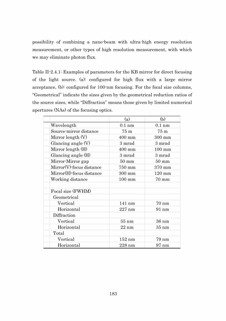
183
possibility of combining a nano-beam with ultra-high energy resolution measurement, or other types of high resolution measurement, with which we may eliminate photon flux. Table II-2.4.1: Examples of parameters for the KB mirror for direct focusing of the light source. (a): configured for high flux with a large mirror acceptance, (b): configured for 100-nm focusing. For the focal size columns, “Geometrical” indicate the sizes given by the geometrical reduction ratios of the source sizes, while “Diffraction” means those given by limited numerical apertures (NAs) of the focusing optics.
(a) (b)Wavelength 0.1 nm 0.1 nmSource-mirror distance 75 m 75 mMirror length (V) 400 mm 300 mmGlancing angle (V) 3 mrad 3 mradMirror length (H) 400 mm 100 mmGlancing angle (H) 3 mrad 3 mradMirror-Mirror gap 50 mm 50 mmMirror(V)-focus distance 750 mm 370 mmMirror(H)-focus distance 300 mm 120 mmWorking distance 100 mm 70 mm
Focal size (FWHM) Geometrical Vertical 141 nm 70 nm Horizontal 227 nm 91 nm Diffraction Vertical 55 nm 36 nm Horizontal 22 nm 35 nm Total Vertical 152 nm 79 nm Horizontal 228 nm 97 nm

184
II-2.4.2. Mirror systems for larger NAs Further increasing NA by using a graded multilayer coating allows
for much smaller focusing, with a sub-10 nm level. To achieve the higher accuracy required for this condition, we introduced adaptive optics, i.e., a deformable mirror that compensates for the excess error of the wavefront by applying the phase retrieval method [Mimura 2010]. We successfully generated a 2D focused spot with a size of less than 10 nm at 20 keV [Yamauchi 2011].
A two-stage focusing system, which consists of two KB focusing systems, was originally developed for the tight focusing of XFEL pulses. The first KB system expands the beam size, while the second one generates a small focus with a large NA. We successfully generated ultra-intense X-ray pulses of 1020 W/cm2 with a size of 30 nm× 55 nm for 9.9-keV XFEL pulses from SACLA [Mimura 2014]. We note that this system is also widely applicable for generating small spots for beamlines with limited length at SPring-8-II. II-2.4.3. Two-dimensional focusing using a single mirror element
Single-mirror focusing, using a mirror such as an ellipsoidal mirror or a Wolter mirror, promises high potential for nano-focusing. Recent breakthroughs with precision machining technology have enabled their development [Motoyama 2014], overcoming the difficulties of complicated and extremely steep profiles. As a prototype, we fabricated an ellipsoidal focusing mirror that has a ring-shaped aperture for the water-window wavelength region [Takei 2013]. The fabrication system consists of mandrel fabrication, surface replication, metrology and refiguring. An objective for the mirror is to focus soft X-ray FEL light to the sub-10 nm region without chromatic aberrations [Motoyama 2013].
For hard X-ray ranges, a grazing-incidence ellipsoidal mirror, which has a very steep curve in the transverse direction to the incident X-rays, is also under development. An advanced stitching interferometer was developed for profiling the three dimensional shape by combining the

185
MSI and the RADSI [Yumoto 2010]. An upgraded EEM [Takei 2014] system will also be combined for fabrication. II-2.4.4. Variable-sized focusing with adaptive optics
Combinative analysis using a flexible focusing size remains challenging, because it is more difficult to change the optical parameters in an X-ray focusing system. An adaptive focusing device [Susini 1995] is a promising candidate for expanding flexibility. 100-nm focusing using piezoelectric deformable mirrors was achieved with bimorphstructure at SPring-8 [Nakamori 2013], using techniques for the at-wavelength wavefront measurement, such as grating interferometry [Matsuyama 2012c].
A drawback of the single adaptive element applied for diffraction limited focusing is the change of the focus position along the optical axis. To overcome this problem, we propose an innovative adaptive focusing optical system comprised of four deformable mirrors arranged in a two-stage Kirkpatrick-Baez configuration, as shown in Fig. II-2.4.1 [Matsuyama 2012a, Kimura 2013]. This optical system can control the spot size at a fixed sample position while maintaining the diffraction-limited focusing by controlling the numerical aperture. We plan to use this system to deliver coherent X-rays with a controllable beam size ranging from one micrometer to a few dozen nanometers for various types of microscopy.
Fig. II-2.4.1: Schematic of a one-dimensional adaptive focusing system. The NA and final focus size are controlled by changing the configuration of the two deformable mirrors (DM1 and DM2). The inset shows an example of coherent diffraction imaging (CDI) and scanning microscopy. Reproduced
186
with permission of the International Union of Crystallography (http://dx.doi.org/10.1107/S1600577514016415). II-2.4.5. Optics for emission spectroscopy with parallel beam geometry
Advances in fabricating aspherical mirror surfaces with unprecedented precision are opening up new optical configurations, e.g., a mirror-based spectrometer, for various types of emission spectroscopy measurements including inelastic X-ray scattering and X-ray nonlinear optics.
Conventionally, cylindrically or spherically bent crystals have been widely used in the Rowland or the von Hamos geometries to disperse divergent X-rays from the samples (Figs. II-2.4.2 (a) and (b)). However, the curvature radius tends to become longer in order to avoid distortion, which enlarges the size of the spectrometer, e.g., ~10-m long. Furthermore, the optical layout is quite limited (for example, multicrystal optics, which is widely used in X-ray monochromators to control the bandwidth, cannot be applied). Now it becomes possible to collimate the divergent beam with aspherical mirrors. Once the beam is made parallel, the spectrometer can be designed more flexibly. A multicrystal spectrometer may be used to achieve sub-meV resolutions. Mirror-based spectrometers may become even more compact.
Here, we present a prototypical mirror-based spectrometer, which consists of a parabolic mirror and a channel-cut analyzer crystal (Fig. II-2.4.2(c)), designed for a future X-ray parametric down-conversion experiment [Tamasaku 2011]. In this nonlinear optical phenomenon, a down-converted X-ray photon is emitted into a small solid angle, e.g., about 1×10⁻⁵ sr, and has a typical bandwidth of about 1 eV around 10 keV. The parabolic mirror is 400-mm long with an effective width of 4 mm, and is manufactured on a fused silica block. The surface is coated with Pt film having a thickness of 60 nm. The roughness and the figure error are measured to be 0.12 nm (rms) and 0.7 nm (rms), respectively. The distance between the sample and the mirror center is set to be 400 mm, and the
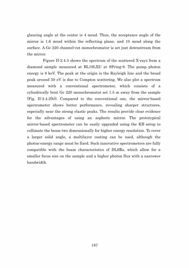
187
glancing angle at the center is 4 mrad. Thus, the acceptance angle of the mirror is 1.6 mrad within the reflecting plane, and 10 mrad along the surface. A Ge 220 channel-cut monochromator is set just downstream from the mirror.
Figure II-2.4.3 shows the spectrum of the scattered X-rays from a diamond sample measured at BL19LXU at SPring-8. The pump photon energy is 8 keV. The peak at the origin is the Rayleigh line and the broad peak around 50 eV is due to Compton scattering. We also plot a spectrum measured with a conventional spectrometer, which consists of a cylindrically bent Ge 220 monochromator set 1.5 m away from the sample (Fig. II-2.4.2(b)). Compared to the conventional one, the mirror-based spectrometer shows better performance, revealing sharper structures, especially near the strong elastic peaks. The results provide clear evidence for the advantages of using an aspheric mirror. The prototypical mirror-based spectrometer can be easily upgraded using the KB setup to collimate the beam two dimensionally for higher energy resolution. To cover a larger solid angle, a multilayer coating can be used, although the photon-energy range must be fixed. Such innovative spectrometers are fully compatible with the beam characteristics of DLSRs, which allow for a smaller focus size on the sample and a higher photon flux with a narrower bandwidth.
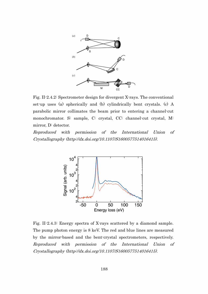
188
Fig. II-2.4.3: Energy spectra of X-rays scattered by a diamond sample. The pump photon energy is 8 keV. The red and blue lines are measured by the mirror-based and the bent-crystal spectrometers, respectively. Reproduced with permission of the International Union of Crystallography (http://dx.doi.org/10.1107/S1600577514016415).
Fig. II-2.4.2: Spectrometer design for divergent X-rays. The conventional set-up uses (a) spherically and (b) cylindrically bent crystals. (c) A parabolic mirror collimates the beam prior to entering a channel-cut monochromator. S: sample, C: crystal, CC: channel-cut crystal, M: mirror, D: detector. Reproduced with permission of the International Union of Crystallography (http://dx.doi.org/10.1107/S1600577514016415).

189
References [Alkire 2000] R. W. Alkire et al., J. Synchrotron Rad. 7, 61 (2000). [Goto 2004] S. Goto et al., AIP Conf. Proc. 705, 400 (2004). [Goto 2007] S. Goto et al., Proc. SPIE 6705, 67050H (2007). [Goto 2011] S. Goto et al., Proc. SPIE 8139, 813910 (2011). [Goto 2012] S. Goto et al., Proc. SPIE 8502, 85020A (2012). [Goto 2014] S. Goto, presented at 8th AOFSRR in Taiwan (2014) (unpublished). [Hanbury-Brown 1956a] R. Hanbury-Brown and R. Q. Twiss, Nature (London) 177, 27 (1956). [Hanbury-Brown 1956b] R. Hanbury-Brown and R. Q. Twiss, Nature (London) 178, 1046 (1956). [Ikonen 1992] E. Ikonen, Phys. Rev. Lett. 68, 2759 (1992). [Ishikawa 2001] T. Ishikawa et al., Proc. SPIE 4145, 1 (2001). [Ishikawa 2012] T. Ishikawa et al., Nat. Photon. 6, 540 (2012). [Jaski 2007] Y. Jaski and D. Cookson, AIP Conf. Proc. 879, 1053 (2007). [Kimura 2013] T. Kimura et al., Opt. Express 21, 9267–9276. [Kirkpatrick 1948] P. Kirkpatrick and A. V. Baez, J. Opt. Soc. Am. 38, 766 (1948). [Matsuyama 2012a] S. Matsuyama et al., Proc. SPIE 8503, 850303 (2012). [Matsuyama 2012b] S. Matsuyama et al., Opt. Express 20, 10310 (2012). [Matsuyama 2012c] S. Matsuyama et al., Opt. Express 20, 24977 (2012). [Mimura 2004] H. Mimura et al., J. Synchrotron Rad. 11, 343 (2004). [Mimura 2005a] H. Mimura et al., Rev. Sci. Instrum. 76, 045102 (2005). [Mimura 2005b] H. Mimura et al., Jpn. J. App. Phys. 76, L539 (2005). [Mimura 2010] H. Mimura et al., Nat. Phys. 6, 122 (2010). [Mimura 2014] H. Mimura et al., Nat. Commun. 5, 3539 (2014). [Mochizuki 2001] T. Mochizuki et al., Nucl. Instr. and Meth. A467-468, 647 (2001). [Mori 2001] Y. Mori et al., Proc. SPIE 4501, 30 (2001). [Motoyama 2013] H. Motoyama et al., Proc. SPIE 8848, 88480E (2013).
190
[Motoyama 2014] H. Motoyama et al., Jpn. J. Appl. Phys. 53, 022503 (2014). [Nakamori 2013] H. Nakamori et al., Nucl. Instr. and Meth. A 710, 93 (2013). [Snigirev 1996] A. Snigirev et al., Nucl. Instr. and Meth. A370, 634 (1996). [Sumiya 2012] H. Sumiya and K. Tamasaku, Jpn. J. Appl. Phys. 51, 090102 (2012). [Susini 1995] J. Susini et al., Rev. Sci. Instrum. 66, 2229 (1995). [Takei 2013] Y. Takei et al., Proc. SPIE 8848, 88480C (2013). [Takei 2014] Y. Takei and H. Mimura, Int. J. Nanomanufact (2014). In the press. [Tamasaku 2001] K. Tamasaku et al., Nucl. Instr. and Meth. A467-468, 686 (2001). [Tamasaku 2005] K. Tamasaku et al., J. Phys. D38, A61 (2005). [Tamasaku 2011] K. Tamasaku et al., Nat. Phys. 7, 705 (2011). [Tamasaku 2014] K. Tamasaku et al., Nat. Photon. 8, 313 (2014). [Tono 2011] K. Tono et al., Rev. Sci. Instrum. 82, 023108 (2011). [Tono 2013] K. Tono et al., New J. Phys. 15, 083035 (2013). [Yabashi 2001a] M. Yabashi et al., Phys. Rev. Lett. 87, 140801 (2001). [Yabashi 2001b] M. Yabashi et al., Rev. Sci. Instrum. 72, 4080 (2001). [Yabashi 2004] M. Yabashi et al., Phys. Rev. A, 69, 023813 (2004). [Yabashi 2007] M. Yabashi et al., AIP Conf. Proc. 879, 922 (2007). [Yabashi 2014] M. Yabashi et al., J. Synchrotron Rad. 21, 976 (2014). [Yamauchi 2002a] K. Yamauchi et al., Rev. Sci. Instrum. 73, 4028 (2002). [Yamauchi 2002b] K. Yamauchi et al., J. Synchrotron Rad. 9, 313 (2002). [Yamauchi 2003] K. Yamauchi et al. Rev. Sci. Instrum. 74, 2894 (2003). [Yamauchi 2005] K. Yamauchi et al., Appl. Opt. 44, 6927 (2005). [Yamauchi 2011] K. Yamauchi et al., J. Phys. Condens. Matter, 23, 394206 (2011). [Yamazaki 2013] H. Yamazaki et al., J. Phys. Conf. Ser. 425, 052001 (2013). [Yumoto 2010] H. Yumoto et al., Nucl. Instr. and Meth. A616, 203 (2010).
191
PART-II II-3 Detector System
II-3.1. Sensors II-3.2. Sensor Variants II-3.3. Detector System II-3.4. Infrastructure to operate coherently with the Detector System
192
II-3. Detector System X-ray imaging detectors will play a key role in the development of
new measurement technologies that are required to fully exploit the upgraded capabilities of SPring-8-II. Each scientific study (and beamline) requires specific detector functions. However, the expected development cost for state-of-the-art X-ray imaging detector systems is so high that establishing dedicated development programs for each individual scientific case is no longer practical. As discussed in Sec. II-1, we must therefore develop a core detector system to cover the baseline scientific needs and we must develop the ability to create alternate configurations of the detector system. The core detector system has functions to detect, visualize, store and analyze the data from the X-ray images. First we discuss the sensors and next aspects of the system design. II-3.1. Sensors
X-rays are detected by sensors. We address four critical demands on sensors, namely, (i) higher quantum efficiency even in the photon energy range of 20-30 keV, (ii) a count rate over 20 Mphotons/pixel/s, (iii) extreme X-ray radiation hardness, and (iv) a fast frame rate, preferably over 209 kHz to synchronize with the revolution frequency of the synchrotron. (i) Higher quantum efficiency even in the photon energy range of 20-30 keV
Silicon is the most widely used material in imaging sensors and electronics. Direct-detection silicon sensors have been proven to offer many advantages such as uniformity, high frame rate, and single-photon detection capability. To cover the higher photon energy regime, however, silicon becomes transparent and quantum efficiency (Q.E.) starts to drop significantly at around 15 keV. Non-silicon material such as CdTe, Germanium or GaAs can provide higher quantum efficiency owing to their higher density, although they have drawbacks such as non-uniformity, lower stability, a lower operation temperature, and/or greater difficulty in manufacturing. To overcome these difficulties, several groups are currently

193
conducting research. Another potential way to increase the Q.E. is using a layered silicon sensor.
In the SPring-8 upgrade plan, we will pursue development using layered silicon sensors. The baseline target is to assemble 3 layers of 0.65 mm thick sensors to form total sensitive thickness of 2 mm, which corresponds to 94% Q.E. at 20 keV, and 60% Q.E. at 30 keV. Each sensor is made using a quasi-monolithic sensor approach in order to maintain the quantum efficiency. The manufacturing process is assumed to be an extension of the monolithic CMOS sensor, SOPHIAS, under development for SACLA [Hatsui2013]. Two types of sensor modules are considered: a single-layer module and a triple-layer module. The baseline implementation uses flip chip bonding to a custom ceramic package. In this case, the layer separation will be about 0.5-1.0 mm. This geometry results in a large parallax. The development of a parallax calibration method must be carried out as well. We will also investigate direct stacking of three sensors layers without spacing in order to reduce the parallax. (ii) A count rate over 20 Mphotons/pixel/s
In many experiments, the maximum count rate is one of the bottlenecks in the overall throughput of the instrument system. This happens especially in experiments that study dynamics, where good statistics are required within a short exposure time. In the conventional photon-counting pixel detector, a maximum count rate is limited by the in-pixel analog circuitry. The typical count rate was reported to be below 5 Mphotons/pixel/s. Rate correction with a retrigger in-pixel circuit was reportedly able to calibrate the rate over 10 Mphotons/pixel/s [Trueb2013]. The maximum count rate has a trade-off with noise, power dissipation, and pixel size, and is difficult to improve significantly without degrading the other performance metrics. To overcome this limit, we will develop an integration pixel with multiple storage cells. We set the target peak count rate as 35 Mphotons/pixel/s for a photon energy of 12.4 keV. Reading out at the frame rate of 21 kHz with a peak signal of 1840 photons/frame gives a native maximum count rate of 38 Mphotons/pixel/s. By differentiating the
194
exposure time for each storage cell, we can effectively increase the peak count rate further. By combining the fast frame rate with alternating short and long exposure times of 1.9 and 47 µs, the effective count rate can be increased by 25 times to 950 Mphotons/pixels/s at the expense of a small increase in the photon shot noise. The sensor will have a global shutter line. The time constant to open and close the electronic shutter will be below 10 ns. The minimum exposure time will be about 100 ns. Thanks to the excellent effective count rate, this sensor can also be used in many of the diffraction experiments where we currently use one-dimensional strip sensors. (iii) Extreme X-ray radiation hardness
The X-ray radiation hardness is governed mainly by the structure of the sensor itself. Silicon dioxide is the major source of degradation as it undergoes a charge buildup after X-ray absorption. We will develop a monolithic sensor process that can resist up to 100 Mrad @ 10 keV by combining industry standard CMOS technology. With a short exposure time, such as 100 ns at a frame rate of 21 kHz, most of the X-rays illuminating the detector are just degrading the sensors. In this case, synchronizing the X-ray shutter to the bunch cycle, which removes the unwanted X-ray beams, will significantly reduce the X-ray dose onto the sensor. The effectiveness of this type of shutter configuration will be investigated in each scientific study. (iv) A fast frame rate, preferably at 209 kHz
The frame rate is determined by the sensor architecture and the production process. With an available complementary metal–oxide–semiconductor (CMOS) technology the feasible frame rate using a 0.3 Mpixel sensor was estimated to be about 21 kHz (Table I). The rate is limited by the analog voltage settling time for the signal transfer from the pixel to the on-chip periphery circuitry, the conversion speed of the column analog-to-digital converter (ADC) in the periphery, the bandwidth of the digital outputs, and power dissipation. Achieving a frame rate of 209 kHz is feasible using an identical design with a region-of-interest operation

195
mode, where about one-tenth of the image section is readout. In the readout mode of the full image section, all of the pixel data is read out at a frame rate of 21 kHz. In both the operation modes, the resulting data rate becomes 184 Gbps for a single sensor chip. II-3.2. Sensor Variants
Once the sensor platform has been established, sensor variants (such as higher time resolution up to 10 ns at the expense of the peak signal, spectroscopy imaging sensor with energy resolution less than 120 eV, or a smaller pixel for 0.5 µm resolution) can be developed at significantly lower cost. The sensor and other components discussed in the next section should be developed by taking into account maximum reuse of the design blocks for future development of these sensor variants. II-3.3. Detector System
An ideal implementation reads out, visualizes, and stores all of the data. However, this type of scheme is not practical simply due to the large data size. A sensor running at 21 kfps with 0.3 Mpixels of bit depth of 30 bits/pixel yields a data rate of 182 Gbps, reaching a data rate of 82.8 TBytes/hour/sensor (Table II-3-1). To cope with data of this size, we will develop proximity electronics, located near the sensor chip. The proximity electronics will have a data memory of 4 GBytes that can store data of about four thousand frames. The field-programmable gate array (FPGA) of the proximity electronics can conduct on-the-fly data analysis. Typical operation modes are listed below. (a) Video mode
Some experiments demand high dynamic ranges, but data acquisition can be slow. In these cases, the sensor chip operates at a frame rate maximum of 21 kHz, and the proximity electronics sum up multiple frames of data into low frequency image data. The presumed frame rate in this mode is a maximum of 1 kHz. (b) Burst mode

196
Some experiments demand acquisition of all of the image data. In these cases, all of the frame data is first buffered within the proximity electronics, and then transferred to the downstream computing server nodes. In this burst mode, X-ray detection and data transfer to the server are done sequentially. The highest bandwidth between the proximity electronics and the server will be implemented by optical link through the high bandwidth serial port of the FPGA. An optical link with 20 Gbps bandwidth will be used for a single sensor chip. The corresponding duty ratio is about 10 %. Data is then cashed on the main memory of the local PC cluster and analyzed by central processing units (CPUs). Analyzed data are stored locally using a wide bandwidth data cache. The burst mode is effective, for example, in destructive measurements, where samples are periodically exchanged. (c) On-the-fly data analysis mode
Some experiments have efficient analysis algorithms which reduces the data rate without losing critical information. One of the simplest cases is pump-probe experiments, where repetition of identical experimental conditions is assumed. Summing the adequate frame data in each cycle drastically reduces the data size. Other on-the-fly algorithms will be investigated in order to fulfill other scientific cases. II-3.4. Infrastructure to operate coherently with the Detector System
Frequently, X-ray image data is analyzed together with other instrument data, such as motor position and timing data of the pump optical laser. From the analysis point of view, X-ray image data is better formatted with a meta-data section containing all the experimental conditions including the other instrument data. Because the frame rate of the X-ray imaging detector is so high, efficient implementation should be investigated. The baseline implementation will have a parameter configuration function. Experiments will be conducted according to their specific parameter configuration, which will be set prior to the data acquisition. The parameter configuration will be sent to the X-ray imaging
197
detector system before the data acquisition starts, and the X-ray imaging system will write the other instrument data into the meta-data section according to the parameter configuration. To complement the parameter configuration scheme, a monitor function will be built to watch over the instruments in order to detect any failure. The synchronization of the X-ray imaging detector system and other instruments should be designed and implemented in a systematic way in order to reduce the costs of development, maintenance, and learning. The implementation details must carefully designed in terms of communication speed, failure patterns, mismatches between the configuration and execution data (as for high precision motors), and dependency on the efficiency of input/output throughput on the data format.
The X-ray imaging detector system will have a local data cache and computation power to diagnose the data quality during the experiment. In some end-stations, where the data volume is lower, the detector system will be able to run as a stand-alone system. However, for many of the beamlines, the local data cache is not large enough and we plan to move large data sets to a global computation infrastructure through seamless archiving software. The computation resources for post analysis should be implemented at the global computation infrastructure. The details of the functions of the global computation infrastructure must be carefully defined and developed. Synergies with the SACLA data analysis framework should also be considered in order to minimize construction and operations costs.
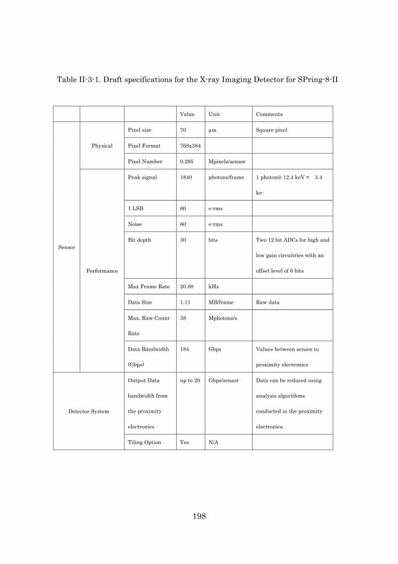
198
Table II-3-1. Draft specifications for the X-ray Imaging Detector for SPring-8-II
Value Unit Comments
Sensor
Physical
Pixel size 70 µm Square pixel
Pixel Format 768x384
Pixel Number 0.295 Mpixels/sensor
Performance
Peak signal 1840 photons/frame 1 photon@ 12.4 keV = 3.4
ke-
1 LSB 60 e-rms
Noise 60 e-rms
Bit depth 30 bits Two 12 bit ADCs for high and
low gain circuitries with an
offset level of 6 bits
Max Frame Rate 20.88 kHz
Data Size 1.11 MB/frame Raw data
Max. Raw Count
Rate
38 Mphotons/s
Data Bandwidth
(Gbps)
184 Gbps Values between sensor to
proximity electronics
Detector System
Output Data
bandwidth from
the proximity
electronics
up to 20 Gbps/sensor Data can be reduced using
analysis algorithms
conducted in the proximity
electronics.
Tiling Option Yes N/A
199
References [Hatsui2013] T. Hatsui, M. Omodani, T. Kudo, K. Kobayashi, T. Imamura,T. Ohmoto,A. Iwata, S. Ono,Y. Kirihara,T. Kameshima, H. Kasai, N. Miura, N. Kuriyama, M. Okihara, Y. Nagatomo, M. Nagasaki, T. Watanabe, M. Yabashi, Proc. Int. Image Sensor Workshop, (2013) Art. Num. 3.05. Online: http://www.imagesensors.org/Past%20Workshops/2013%20Workshop/2013%20Papers/03-5_058_hatsui_paper.pdf [Trueb2013] P. Trueb et al., Journal of Physics: Conf. Ser. 425 (2013) 062002.

200
Appendix Contributing Authors
Yoshihiro Asano Takashi Ohshima Teruhiko Bizen Masaya Oishi Hiroyasu Ego Yuichi Okayasu Takahiro Fujita Yuji Otake Kenji Fukami Shigeki Sasaki Toru Fukui Yoshito Shimosaki Shunji Goto Kouichi Soutome Toru Hara Takashi Sugimoto Takaki Hatsui Sunao Takahashi Takahiro Inagaki Shiro Takano Tetsuya Ishikawa Masaru Takao Kimitaka Kaneki Hideki Takebe Hirokazu Maesaka Kenji Tamasaku Mitsuhiro Masaki Hitoshi Tanaka Tomohiro Matsushita Ryotaro Tanaka Satoshi Matsuyama Takashi Tanaka Hidekazu Mimura Kensuke Tono Chikaori Mitsuda Takahiro Watanabe Takeshi Nakamura Makina Yabashi Haruhiko Ohashi Kazuto Yamauchi Haruo Ohkuma