spatial light modulators - lastek.co.kr · company structure. comments on driving ... ti 3panel...
TRANSCRIPT


SPATIAL LIGHT MODULATORS
AND APPLICATIONS - OVERVIEW
HOLOEYE Photonics AG

CONTENT
• Introduction
• Comments on driving forces for SLM development
• SLM-Technologies
• Requirements for micro-displays in Technical Optics
• Applications
• Comments on actual developments in micro-display industry

• Products and services related to diffractive micro-optics
• R&D in the field of diffractive optics
• Active Spatial Light Modulators – a[SLM]
• Micro-display technologies for technical optics
HOLOEYE Photonics AGAlbert-Einstein-Strasse 14Berlin, 12489, Germany
Phone/ Fax: +49 (0)30 6392-3660/ -3662
www.holoeye.com
HOLOEYE Corporation23151 Verdugo Dr., Suite 114Laguna Hills, CA 92653-1340
Phone/ Fax: (949) 461-7064/ 581-6838
www.holoeyecorp.com
HOLOEYE – Core Technologies

DOE SERVICES
Director
Andreas Hermerschmidt
Micro-Display - OEM
Director
Ulli Hendricks
a[SLM]
Director
Sven Krüger
Delivers the complete supply-chainDesign, mastering and replication in various materials and quantities
Current Focus: R&D and SME
Future Focus: Large Companies – OEM
Various types of a[SLM]:LC2002, LC-R 2500, LC-R 768, LC-R 720, LC-R 1080
Focused on R&D customers; large array of applications
Strong communication between HOLOEYE and these customers enables transfer of IP for future product developments
Strategic Partnership with BRILLIAN Corp., AZSupplies Brillian´s Displays for all niche markets, ranging from medical to commercial to defense applications
Strategic Partnership with BALLISTA, Inc., CAadditional offer of complete one-stop-solutions (displays, electronics, complete optical-engines)
COMPANY STRUCTURE

Comments on driving forces for SLM development
• Actual SLM-systems are either MEMS-based or LCD based
• Most micro-LCD developments are driven by consumer electronics industry for RPTV and front projectors
• Also MEMS-technologies such as DLP or GLV are driven by consumer electronics industry
• Some industrial applications forced optical MEMS development for scanning, printing technologies and also for automotive applications
• The only R&D related driving force for new SLM-technologies is the defense industry
TI 3Panel DLP-Developer Kit
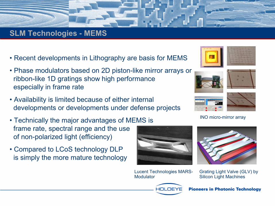
SLM Technologies - MEMS
Grating Light Valve (GLV) by Silicon Light Machines
INO micro-mirror array
Lucent Technologies MARS-Modulator
• Recent developments in Lithography are basis for MEMS
• Phase modulators based on 2D piston-like mirror arrays or ribbon-like 1D gratings show high performance especially in frame rate
• Availability is limited because of either internal developments or developments under defense projects
• Technically the major advantages of MEMS is frame rate, spectral range and the use of non-polarized light (efficiency)
• Compared to LCoS technology DLP is simply the more mature technology

Analog Devices' ADXL50 accelerometer
Pressure Sensor
• MEMS are all around
• Phase modulators and other optical implementations are niche markets for MEMS industry
• Customized MEMS development is still quite challenging and expensive – so it was for LCDs
• LCDs still have an advantage out of their driving force (RPTV market) in terms of resolution and minimal pixel size for 2D displays
• Some application require a polarization modulated wave field, best to be achieved with LCoS
SLM Technologies – MEMS ans LCDs

SLM - Spatial Light Modulators based on LC-displays
A New Generation of Optical Components:• Amplitude and phase modulation due to polarization rotation and/ or controlled birefringence• Modulation with a high Space-Bandwidth-Product (Pixel Number – Pixel Pitch – Dynamic Range)• Numerous applications as adaptive/addressable optical components• Addressing frame rate in video frequencies (60 – 72 Hz) up to kHz- frame rates for FLC-Systems• High light efficiency with reflective LCoSTM displays in all applications

Applications for Projection and Phase Modulation
Projection• Printer applications (Imaging, 3D)
• Optical Metrology and Fringe Projection
• Special projection applications (Simulation, Lithography)
• HUDs and HMDs in airborne and defense industries
• HUDs for automotive applications
• SLMs for R&D
• High resolution NTE applications (viewer)
Phase Modulation• Telecommunication (WDM, optical interconnection, switching)
• Holographic security systems
• SLMs for R&D
• Rapid DOE prototyping
• Dynamic calibration
• Bio-Photonics applications (micro-displays in microscopy)
• Wave front generation
• Digital Holography, dynamic diffractive optics

SLM – Applications
HOLOEYE´s SLM technology has now been utilized by over 150 companies, universities, and research institutes around the world.
Applications include:- Bio-Photonics- Optical Metrology- Holography (Display holography, holographic memory, holographic recording and security systems, including digital holography)- Beam splitting and beam shaping- Optical interconnection such as switching and information encoding- Interferometry- Material processing

FISBA - wave front control in interferometers
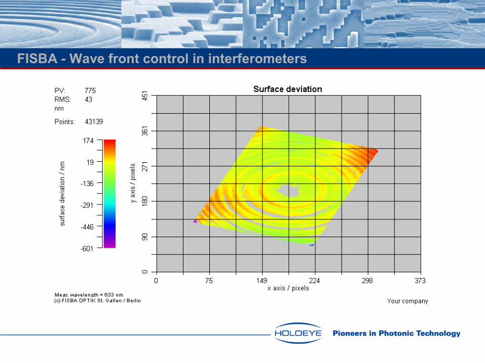
FISBA - Wave front control in interferometers

Applications – Wave front correction
SLM
H.-S.
Lase
r 543
nm
PC
Application
Set-up closed loop wave-front control

x [mm]
W[wavelength]
y[mm]
0/0
3.844
03.15
3.15
Open loop wave front
x [mm]
W[wavelength]
y[mm]
0/0
0.272
03.15
3.15
Closed loop wave front
SLM Phase Distribution
Features
Peak valley ~ 0.25λ Bandwidth ~ 0.1Hz
15 Legendre Modes corrected
Test of closed loop wave front control
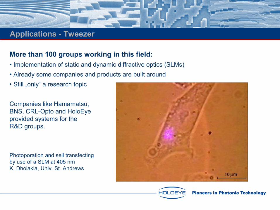
Applications - Tweezer
More than 100 groups working in this field:• Implementation of static and dynamic diffractive optics (SLMs)• Already some companies and products are built around• Still „only“ a research topic
Companies like Hamamatsu, BNS, CRL-Opto and HoloEye provided systems for theR&D groups.
Photoporation and sell transfectingby use of a SLM at 405 nmK. Dholakia, Univ. St. Andrews

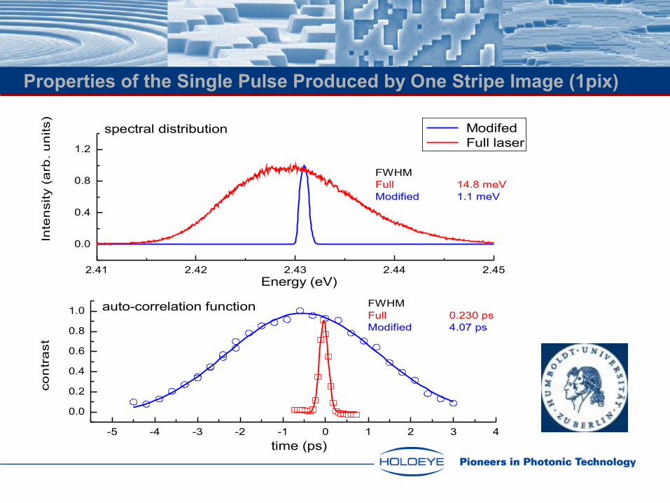
Application – Pulse shaping

Application – Pulse shaping
Grating
Polariser
Slit
SLM
two-color pump-probe
Double stripe image is used in case oftwo optical pulses with different frequency
“The width of the stripes was always taken small, i.e. not more than 5 pix, which is comparable with the resolution of the mini-spectrometer used to disperse the light. The reason is the following – to achieve the spectral shape – close to Gaussian - without varying the grey scale inside the stripe.„
2.41 2.42 2.43 2.44 2.45
0.0
0.4
0.8
1.2
-5 -4 -3 -2 -1 0 1 2 3 4
0.0
0.2
0.4
0.6
0.8
1.0
spectral distribution
FWHMFull 14.8 meVModified 1.1 meV
Inte
nsi
ty (
arb
. u
nits
)
Energy (eV)
Modifed Full laser
FWHMFull 0.230 psModified 4.07 ps
auto-correlation function
con
tra
st
time (ps)
Properties of the Single Pulse Produced by One Stripe Image (1pix)

Applications – Dynamic Calibration of opto-electronic sensors
HOLOEYE has developed a technique for calibrating optical sensor systems through the use of active spatial light modulators and/or diffractive optical elements.
Spatial calibration of optical sensors considers:
• Spherical and chromatic aberration of the optical system• Orientation of optics and sensor with respect to the optical axis• Inner-Orientation (i.e. The orientation of the optics relative to the sensor)
Diffraction grating

Instead of imaging a calibrated range HOLOEYE is using diffractive optics to generate reference beams of high angular accuracy to derive the aberrations and subsequently, generate a digital look-up table.
The Solution

The types of cameras that require spatial calibration are numerous:
• Satellite imaging systems;
• High-resolution cameras for 1D and 2D cartographic mapping;
• Industrial machine vision systems;
• IR and thermal imaging systems; and even
• Low-Cost commercial CCD-based digital cameras, where the optimization of the imaging capabilities is important due to the use of low-cost optics.
Camera Systems
Forest Fire Camera

Advantages
• Complete “field of view” calibration with one capture
• Geometrical pattern position independent from DOE position
• Translation invariant in x,y
• Measuring of chromatic aberration using different wavelengths
• Dynamic approach using SLM technology increases application field
• Compact, mobile, low-cost solution
Image taken with an Olympus E1 camera. The CCD sensor „looks“ through the DOE
onto the pin hole.

The implementation of this technology products and services:
• Calibration systems (alignment of components) in high-performance camera manufacturing
• Implemented (i.e. inflight) calibration systems
• Calibration services - mobile calibration systems
Development potential of the products and services
• Combination of static DOE and a SLM technology
• 2D and 1D sensors
• Calibration of Zoom lenses due to 3D calibration patterns
• CCD sensors, thermal sensors (i.e. pyro-electric sensors)
• Complex optical components (e.g. optical engines)
Implementation

Micro-Display technology has found numerous applications in the printing industry (film exposure, photo prints, projection systems) as well as in lithography. Dynamic, high-resolution, micro-display based holographic mastering systems were developed to service the Holographic Security industry.
Products and Services:• Transaction Cards• Bank Notes and Documents of Value• Product Authentication• Identification Documents• Security Packaging• Commercial Holography
One challenge currently being undertaken is the development of a dynamic, high-resolution holographic encoding system for individual data in passports.
Holographic Mastering

Application – Holography, Lithography
Optical Data Storage in Azobenzene Polyesters
• Polymer film is initially isotropic
• After irradiation with polarized light, azobenzene aligns perpendicular to polarization
• This causes a change in refractive index which is locked into position due to polymer chains
• Heat or circularly polarized light causes random reorientation, erasing the stored information

Application – Holography, Lithography
Isotropic photopolymer
Polarized illumination
Patterned, anisotropic photopolymer (refractive
index changed)
Polymers are photosensitive between 400 nm and 550 nm; High diffraction efficiency (>50%); High resolution (>5000 lines/mm), Long storage life (>12 years for aliphatic systems), Erasable and rewritable; Fast response time (<100 ps)

Application – Holography, Lithography
Holographic Memory Card
HMC Read/Write unit
HMC Read-Only unit

Application – Holography, Lithography
Micro-display technology is used for holographic mastering for object, or object sequence representation but also to code the object wave in a phase representation.
Resolution of sub-micron has been achieved.
The combination of SLMs and photolithography set-ups is currently an issue, where modulators are used as addressable amplitude or phase mask or as diffraction grating to expose the photo resist with dynamic diffraction patterns.

Application – Laser Material Processing
SLM as design tool and in rapid prototyping:
• High damaging threshold (~50 mJ/cm²)
• Implementation as test device for beam shaping tasks
• SLMs as tool for the design and implementation
• Implementations as dynamic mask and dynamic diffraction grating

LC2002 – 800 x 600 pixel, 32µm, 8 Bit, 60 Hz, VGA
LC-R 1080- 1920 x 1200 pixel, 8.1µm, 8 Bit, 60 Hz, DVI
LC-R 2500 – 1024 x 768 pixel, 19µm, 8 Bit, 75 Hz, DVI
LC-R 768 – 1280 x 768 pixel, 12µm, 8 Bit, 60 Hz, DVI
LC-R 720 – 1280 x 768 pixel, 20µm, 8 Bit, 60 Hz, DVI
SLM - Spatial Light Modulators

• Development of micro-display based Spatial Light Modulator systems – commercial systems
LC 2002 – based on 1,3“ SVGA display
LC-R 3000 – based on 0,85“ WUXGA LCoS display
LC-R 2500 – based on 0,97“ XGA LCoS display
LC-R 768 – based on 0,7“ WXGA LCoS display
LC-R 720 – based on 1,18“ WXGA LCoS display
LC-R 1080 – based on a 0,7”1920 x1200 display - 8,1 µm
HOLOEYE Microdisplay Systems

Micro-display Industry
How to bring Micro-display technology into new Applications?• Manufacturers are mainly focused on the consumer electronics market• Technology is specified for consumer electronics applications• Manufacturers have no resources for characterizing their products for other applications• There is no implementation assistance • There is no hardware of the latest micro-display technology available
HOLOEYE wants to fill this gap!• We offer implementation assistance • We can offer development of customized LC displays based on the latest micro-display backplane technology available

Primary Focus:• Transfer of micro-display technologies into the field of technical optics; applications ranging from medical, commercial, defense, and others • Strong cooperation with BRILLIAN, Corp., AZ (Sales and Technical Assistance)• Strong cooperation with BALLISTA, Inc., CA (Enables complete solutions by access to optical engines)• Constantly evaluating new applications for future products
MICRODISPLAY SERVICES – OEM

• Display technologies (transmissive, reflective)• LC-mode (ferroelectric, twisted nematic, VAN)• Resolution• Pixel size (pitch)• Geometrical dimensions
MICRODISPLAY SERVICES– OEM – Customer Display Requirements

MICRODISPLAY SERVICES –OEM– Customer Electronics Requirements
• Signal sources (Video, VGA, DVI, etc.)• Frame rates (display technology related)• Light source• Geometrical dimensions

MICRODISPLAY SERVICES – OEM – Standard Products
• Translucent OEM
8 Bit DVI-Input system for: 0.9“ XGA display, 1.8“ XGA display
12 Bit DVI-Input systems for:0.9“ XGA display, 1.8“ XGA display
• Reflective OEM
Philips DD720
Brillian 768 (Cholla board)
Brillian BR1080HC (1920x1080)
Brillian NTE BR86 (color sequential)

Phase Modulator based on 1920x1200 – 8 micron pitch backplane
• We do have a project for a HDTV phase modulator able to realize clearly 2 π phase shift in the visible an d near IR
• Send me you wish-list for such a device!