si photonic crystal slow-light modulators with … jlt 2017.pdf1684 journal of lightwave technology,...
TRANSCRIPT
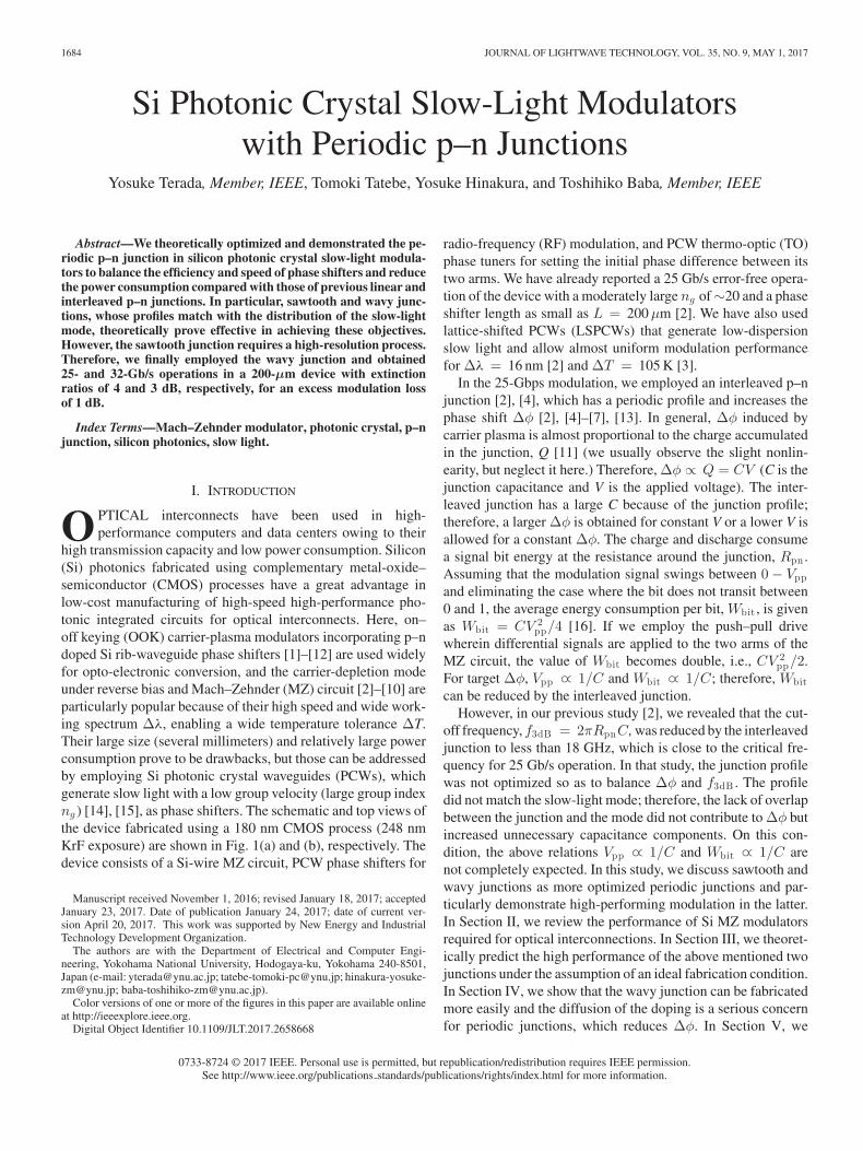
1684 JOURNAL OF LIGHTWAVE TECHNOLOGY, VOL. 35, NO. 9, MAY 1, 2017
Si Photonic Crystal Slow-Light Modulatorswith Periodic p–n Junctions
Yosuke Terada, Member, IEEE, Tomoki Tatebe, Yosuke Hinakura, and Toshihiko Baba, Member, IEEE
Abstract—We theoretically optimized and demonstrated the pe-riodic p–n junction in silicon photonic crystal slow-light modula-tors to balance the efficiency and speed of phase shifters and reducethe power consumption compared with those of previous linear andinterleaved p–n junctions. In particular, sawtooth and wavy junc-tions, whose profiles match with the distribution of the slow-lightmode, theoretically prove effective in achieving these objectives.However, the sawtooth junction requires a high-resolution process.Therefore, we finally employed the wavy junction and obtained25- and 32-Gb/s operations in a 200-µm device with extinctionratios of 4 and 3 dB, respectively, for an excess modulation lossof 1 dB.
Index Terms—Mach–Zehnder modulator, photonic crystal, p–njunction, silicon photonics, slow light.
I. INTRODUCTION
O PTICAL interconnects have been used in high-performance computers and data centers owing to their
high transmission capacity and low power consumption. Silicon(Si) photonics fabricated using complementary metal-oxide–semiconductor (CMOS) processes have a great advantage inlow-cost manufacturing of high-speed high-performance pho-tonic integrated circuits for optical interconnects. Here, on–off keying (OOK) carrier-plasma modulators incorporating p–ndoped Si rib-waveguide phase shifters [1]–[12] are used widelyfor opto-electronic conversion, and the carrier-depletion modeunder reverse bias and Mach–Zehnder (MZ) circuit [2]–[10] areparticularly popular because of their high speed and wide work-ing spectrum Δλ, enabling a wide temperature tolerance ΔT.Their large size (several millimeters) and relatively large powerconsumption prove to be drawbacks, but those can be addressedby employing Si photonic crystal waveguides (PCWs), whichgenerate slow light with a low group velocity (large group indexng ) [14], [15], as phase shifters. The schematic and top views ofthe device fabricated using a 180 nm CMOS process (248 nmKrF exposure) are shown in Fig. 1(a) and (b), respectively. Thedevice consists of a Si-wire MZ circuit, PCW phase shifters for
Manuscript received November 1, 2016; revised January 18, 2017; acceptedJanuary 23, 2017. Date of publication January 24, 2017; date of current ver-sion April 20, 2017. This work was supported by New Energy and IndustrialTechnology Development Organization.
The authors are with the Department of Electrical and Computer Engi-neering, Yokohama National University, Hodogaya-ku, Yokohama 240-8501,Japan (e-mail: [email protected]; [email protected]; [email protected]; [email protected]).
Color versions of one or more of the figures in this paper are available onlineat http://ieeexplore.ieee.org.
Digital Object Identifier 10.1109/JLT.2017.2658668
radio-frequency (RF) modulation, and PCW thermo-optic (TO)phase tuners for setting the initial phase difference between itstwo arms. We have already reported a 25 Gb/s error-free opera-tion of the device with a moderately large ng of ∼20 and a phaseshifter length as small as L = 200 μm [2]. We have also usedlattice-shifted PCWs (LSPCWs) that generate low-dispersionslow light and allow almost uniform modulation performancefor Δλ = 16 nm [2] and ΔT = 105 K [3].
In the 25-Gbps modulation, we employed an interleaved p–njunction [2], [4], which has a periodic profile and increases thephase shift Δφ [2], [4]–[7], [13]. In general, Δφ induced bycarrier plasma is almost proportional to the charge accumulatedin the junction, Q [11] (we usually observe the slight nonlin-earity, but neglect it here.) Therefore, Δφ ∝ Q = CV (C is thejunction capacitance and V is the applied voltage). The inter-leaved junction has a large C because of the junction profile;therefore, a larger Δφ is obtained for constant V or a lower V isallowed for a constant Δφ. The charge and discharge consumea signal bit energy at the resistance around the junction, Rpn .Assuming that the modulation signal swings between 0 − Vppand eliminating the case where the bit does not transit between0 and 1, the average energy consumption per bit, Wbit , is givenas Wbit = CV 2
pp/4 [16]. If we employ the push–pull drivewherein differential signals are applied to the two arms of theMZ circuit, the value of Wbit becomes double, i.e., CV 2
pp/2.For target Δφ, Vpp ∝ 1/C and Wbit ∝ 1/C; therefore, Wbitcan be reduced by the interleaved junction.
However, in our previous study [2], we revealed that the cut-off frequency, f3dB = 2πRpnC, was reduced by the interleavedjunction to less than 18 GHz, which is close to the critical fre-quency for 25 Gb/s operation. In that study, the junction profilewas not optimized so as to balance Δφ and f3dB . The profiledid not match the slow-light mode; therefore, the lack of overlapbetween the junction and the mode did not contribute to Δφ butincreased unnecessary capacitance components. On this con-dition, the above relations Vpp ∝ 1/C and Wbit ∝ 1/C arenot completely expected. In this study, we discuss sawtooth andwavy junctions as more optimized periodic junctions and par-ticularly demonstrate high-performing modulation in the latter.In Section II, we review the performance of Si MZ modulatorsrequired for optical interconnections. In Section III, we theoret-ically predict the high performance of the above mentioned twojunctions under the assumption of an ideal fabrication condition.In Section IV, we show that the wavy junction can be fabricatedmore easily and the diffusion of the doping is a serious concernfor periodic junctions, which reduces Δφ. In Section V, we
0733-8724 © 2017 IEEE. Personal use is permitted, but republication/redistribution requires IEEE permission.See http://www.ieee.org/publications standards/publications/rights/index.html for more information.

TERADA et al.: SI PHOTONIC CRYSTAL SLOW-LIGHT MODULATORS WITH PERIODIC P–N JUNCTIONS 1685
Fig. 1. Si PCW MZ modulator. (a) Schematic. (b) Total view of fabricateddevice and scanning electron micrograph (SEM) of p–n doped PCW. The latteris colored to show the p–n junction boundary. (c) Transmission (upper) and ng
(lower) spectra of PCW with neither lattice shifts nor p–n doping.
demonstrate the measured results of Δφ and 25–32 Gb/s modu-lation, which are beyond the previous results obtained using theinterleaved junction.
II. REQUIREMENTS
The requirement for OOK modulators in optical interconnectsdepends upon the power consumption of the optical transceiversand the total systems. An example of such requirements
Fig. 2. Δφ required for ER.
considered in this study include a bit rate BR � 25 Gb/s, anextinction ratio ER � 3 dB, a phase-shifter length L � 1 mm, anon-chip insertion loss Loss � 5 dB, and a temperature toleranceΔT � 100 K (or the corresponding working spectrum Δλ �8 nm). Our PCW slow-light modulator satisfies the requirementfor L and ΔT (or Δλ). In this study, we fixed L = 200 μmbecause a longer L increases the insertion loss. The insertionloss is given by the passive loss and the modulation-excessloss, ML. The passive loss is composed of (i) scattering losscaused by structural disordering of fabricated PCWs, (ii) free-carrier absorption caused by doping, (iii) connection loss be-tween the wire waveguide and PCW, and (iv) excess loss oftwo multimode-interference-type 1 × 2 couplers in the MZ cir-cuit. Fig. 1(c) shows the transmission spectrum of the fabricatedundoped 200 μm PCW normalized by that of the same-lengthSi-wire waveguide. From this transmission band, the sum of (i)and (iii) is estimated to be 1–2 dB. This value can be reducedby employing a more advanced CMOS process and optimiza-tion of the connection structure. The total excess loss of the twooptimized 1 × 2 couplers is ∼0.5 dB [17]. Thus, the sum of (i),(iii), and (iv) will not be greater than 2 dB.
Focusing on (ii) and ML, which is related to ER, if the initialphase difference between two arms of the MZ circuit is set closeto π by using TO phase tuners, we can obtain a large ER with asmall Δφ. However, this initial phase difference causes a largeML and degrades the signal-to-noise ratio, S/N. ML should bereduced, while ML = 0 dB requires a particularly large Δφfor the target ER. Therefore, minimizing the total loss by addinga moderate ML is a good strategy. Δφ required for a target ERand a given ML in [dB] is expressed as
Δφ = arccos(2 · 10−0.1(M L+ER) − 1
)
− arccos(2 · 10−0.1M L − 1
)(1)
and calculated, as shown in Fig. 2. Δφ = 0.50π is necessary forER = 3 dB and ML = 0 dB, whereas Δφ = 0.27π is nec-essary for ML = 1 dB. In the previous PCW modulator, ERexhibited a ∼1 dB fluctuation because of the fluctuation in theng spectrum [2]. This fluctuation can be reduced by optimiz-ing the connection structure and suppressing unwanted internal

1686 JOURNAL OF LIGHTWAVE TECHNOLOGY, VOL. 35, NO. 9, MAY 1, 2017
resonance; still ER > 4 dB would be desired to compensate forthis fluctuation, and Δφ = 0.32π is necessary for ML = 1 dB.
For high-speed modulators, Δφ is limited by f3dB , which isdominated by the RC time constant and also affected by thephase mismatch between slow light and RF signal [2]. Thephase mismatch becomes severe when the phase shifter is elon-gated, ng is enhanced, and BR is increased. In the discussionof this paper, we impose the limits L = 200 μm, ng ≈ 20,and BR = 25-32 Gb/ s to neglect the phase mismatch. Theequivalent circuit of the modulator is then simplified to a se-ries of internal resistance of pulse-pattern generator (PPG), R0 ,Rpn , and C [see Fig. 3(a)]. The capacitance voltage, VC (t),for operating the phase shifter is related to the PPG voltage,V0(t), as
dVC(t)dt
+VC(t)RC
=V0(t)RC
(2)
where R = R0 + Rpn . We observed the waveform of the RFsignal from the PPG (Anritsu MP1800A, MU183020A; thehighest BR is 32 Gb/s) actually used in this experiment us-ing a sampling oscilloscope, and the rise and fall of V0(t) wasestimated as
Vin,rise(t) = V0
[1 − exp
{−(
t
τ
)3}]
(3)
Vin,fall(t) = V0 exp
[−(
t
τ
)3]
(4)
where τ = 18 ps. From Eqs. (2)–(4),
VC ,rise(t, VC0) = V0
[1 − exp
(− t
RC
)]
+ exp(− t
RC
)[VC0 − V0
RC
∫ t
0
× exp
(−(
t′
τ
)3
+t′
RC
)dt′]
(5)
VC ,fall(t, VC0) = exp(− t
RC
)[VC0 +
V0
RC
∫ t
0
× exp
{−(
t′
τ
)3
+t′
RC
}dt′]
. (6)
When the RF signal is a pseudo-random bit sequence (PRBS),the above two VC (t) form an eye pattern. Assuming Δφ ∝VC(t), similar eye patterns are formed in the phase differ-ence between the two arms, φ. Examples of such eye pat-terns are shown in Fig. 3(b) and (c). The eye starts to closewhen the frequency component of the RF signal approachesf3dB = 1/2πRC. The difference between the local maximumof VC(t) for a sequence . . . →0→0→1→0→0→ . . . and thelocal minimum for . . . →1→1→0→1→1→ . . . gives the valueof the eye opening and effective Δφ in the modulation (RF Δφ).
Fig. 3. Analysis of transient response characteristics. (a) Lumped circuitmodel. (b) and (c) Transient response of phase at 25 and 32 Gb/s, respectively.(d) RF Δφ/DC Δφ calculated with f3dB .
For the timing of the maximum open eye, tm ,
RFΔφ =1V0
⎛⎜⎜⎝
VC ,fall
(tm , VC ,rise
(1
BR, 0))
−VC ,rise
(tm , VC ,fall
(1
BR, V0
))
⎞⎟⎟⎠DCΔφ
(7)

TERADA et al.: SI PHOTONIC CRYSTAL SLOW-LIGHT MODULATORS WITH PERIODIC P–N JUNCTIONS 1687
Fig. 4. Studied p–n junction profiles. (a) Total image including electrodes. (b) Linear junction. (c) Interleaved junction. (d) Sawtooth junction. (e) Wavy junction.
Fig. 5. (a) Average intensity distribution of slow-light mode at k = 0.405(2π/a). (b)–(e) Distribution of ΔnSi for each junction.
where DC Δφ is that not including the high-speed response.Fig. 3(c) shows the RF Δφ/DC Δφ calculated with f3dB , indi-cating that the reduction of f3dB by excessively increasing C ina deep interleaved junction severely reduces RF Δφ.
III. THEORETICAL PERFORMANCE
Four types of p–n junctions are theoretically analyzed, asshown in Fig. 4, to find the one junction that is well-balancedbetween DC Δφ and f3dB , resulting in the highest RF Δφ. Par-ticular attention is given to sawtooth and wavy junctions andthey are compared with linear and interleaved junctions. Thelongitudinal pitch, p, of the interleaved junction is set to a pre-viously determined value, 600 nm. For the sawtooth and wavyjunctions, we set p = 400 and 800 nm, respectively, and thejunction width, wy , as a free-design parameter. Other parame-ters are kept similar to those in [4]; the refractive indices of Siand silica cladding are 3.48 and 1.44, respectively; Si thicknessis 210 nm; lattice constant of the PCW is a = 400 nm; hole di-ameter is 2r = 210 nm; doping concentrations are NA (accep-tor) = 1.05 × 1018 cm−3 and ND (donor) = 6.2 × 1017 cm−3 ;
concentration at the p+ and n+ regions for the ohmic contact isN+
A = N+D = 1.9 × 1020 cm−3 ; and distance between these
regions is W = 4 μm (the distance between electrodes is alsoset at W ′ = 10 μm, but the result is not sensitive to this value).
An example slow-light mode distribution, |E|2, in the PCWis shown in Fig. 5(a). In this study, the distribution is averagedby taking the square of the Fourier transform of the modal timeevolution at each position. Large |E|2 appears periodically atthe center of the waveguide and near the first-row of holes. Thisfigure assumes a propagation constant of k = 0.405(2π/a),but the distribution does not change much for other values of kin the transmission band. When the reverse bias, VDC , is appliedto the junction, the carrier densities are changed by ΔNn,p andthe index of Si is locally changed by ΔnSi , which is expressedas [18]
ΔnSi = −8.8 × 10⁻⁴ΔNn − 2.1 × 10⁻³ΔNp0.8 (8)
where ΔNn,p are in units of 1018 cm−3. We calculated thedistribution of ΔNn,p using a commercial simulator, LumericalDEVICE, and obtain the distribution of ΔnSi for the voltageswing VDC = 0 − 3.0 V, as shown in Fig. 5(b)–(e). Large ΔnSi

1688 JOURNAL OF LIGHTWAVE TECHNOLOGY, VOL. 35, NO. 9, MAY 1, 2017
Fig. 6. Performance of PCW phase shifter with linear p–n junction and ng
spectrum. (a) DC Δφ. (b) Loss.
occurs at the edges of the depletion region around the p–njunction, and ΔnSi = 0 appears between the edges because thedepletion region already exists at VDC = 0V. We calculatedthe change of modal equivalent index, Δneq , using thefollowing formulas [4]:
Δneq =∫
ΔnSi|E|2dxdydz∫ |E|2dxdydz= Γslab
∫ΔnSi|E|2dxdy∫ |E|2dxdy
(9)
Γslab =
∫slab |E|2dxdydz∫all |E|2dxdydz
(10)
where Γslab is the confinement factor of the slow-lightmode into the photonic crystal slab, which was calculated asΓslab = 0.73 − 0.74 for different k. A large Δneq is expectedfor the sawtooth and wavy junctions because their profilesoverlap with the mode maxima. Δφ is given by
Δφ = ΔkL = k0ngΔneq
nSiζL ζ = − dnSi
dneq
nSi
ωb
dωb
dnSi(11)
where k0 is the wavenumber in vacuum and ωb is the frequencyof the photonic band. We slightly modify the definition of ζfrom that in [2], [4] for easy calculation; from the photonic bandcalculation, ζ = 1.45 − 1.57 is obtained for different k. Sincethe mode distribution and ng vary with k and correspondingwavelength in the PCW, Δφ also varies. The spectrum of DCΔφ obtained for the linear junction, as an example, is shownin Fig. 6(a), with the ng spectrum obtained from the slope ofthe photonic band [15]. DC Δφ increases with the increasein ng toward the band-edge wavelength. The loss because offree carrier absorption is also shown with ng in Fig. 6(b). It
Fig. 7. Comparision of performance between four junctions. (a) DC Δφ.(b) C and Wbit . (c) f3dB . (d)–(f) RF Δφ at different BRs. λ = 1564 nm.VDC = 0 − 3 V.
increases similarly to DC Δφ, but the increase is also observedat shorter wavelengths exhibiting lower ng . This is because ofthe increase of mode spreading toward the n+ and p+ regions.
We calculated DC Δφ, C, Wbit , f3dB , and RF Δφ,assuming ng = 22 and the push-pull drive, as shown inFig. 7. The linear junction (dashed line) shows high speed andsmall Wbit , but Δφ is so small that the eye opening is limited.DC Δφ for VDC = 0 − 3.0 V increases with increasing wy [seeFig. 7(a)]. It then decreases for the interleaved and wavy junc-tions because these junctions particularly overlap with the holesfor large wy . At wy = 400 nm, DC Δφ ∼ 0.45π is expectedfor these periodic junctions. According to Fig. 2, this valueallows ER = 3 dB even with ML < 0.2 dB, or ER > 8 dBwith ML = 1 dB. The difference between these periodic junc-tions is not significantly large; however, the interleaved junctionappears to be slightly advantageous compared with others. Re-garding C, we calculate Q at the center voltage, VDC = −1.5 V,and apply the relation C = dQ/dVDC . Unlike DC Δφ, Cdefinitely decreases for the sawtooth and wavy junctions [seeFig. 7(b)]. Wbit estimated from CV 2
pp/2 for the push–pull driveis as small as 0.3 pJ/bit for the sawtooth and wavy junctionsat wy = 400 nm, which is approximately 70% of that for theinterleaved junction and much smaller than that for the conven-tional rib-waveguide modulators, i.e., 4.2 pJ/bit [10]. f3dB is

TERADA et al.: SI PHOTONIC CRYSTAL SLOW-LIGHT MODULATORS WITH PERIODIC P–N JUNCTIONS 1689
Fig. 8. Design of p–n junction (upper) and SEM image of fabricateddevice in which surface etching occurred at p-type ion implantation (lower).(a) Interleaved junction. (b) Sawtooth junction. (c) Zigzag (wavy) junction.
determined from Rpn and C. Compared with the rib-waveguidemodulators, the slow-light mode in the PCW penetrates twice asfar into the photonic-crystal claddings. To avoid absorption loss,W must be increased appropriately, resulting in increased valueof Rpn . Actually, Rpn = 52Ω was calculated for the afore-mentioned W and doping concentration. A slightly larger valueof Rpn is often measured for fabricated devices because of thepresence of non-activated dopants near the periphery of the holes[8]; therefore, we assume Rpn = 60Ω, in this study. Addingthe internal resistance of PPG (R0 = 50Ω), we set R = 110Ωand calculate f3dB = 1/2πRC [see Fig. 7(c)]. The sawtoothand wavy junctions exhibit higher f3dB , although it is graduallyreduced by increasing wy . The interleaved junction exhibits alower value because of excess capacitance. We finally obtain RFΔφ by setting Vpp = 3.0 V and VDC = −1.5 V, which corre-spond to the values assumed for DC Δφ and f3dB , and substi-tuting the obtained value of DC Δφ and f3dB into Eqs. (5)–(7).At wy = 400 nm, RF Δφ for the wavy junction shows maxi-mum values of 0.41π–0.37π at 25–32 Gb/s, which allows ER> 4 dB with ML = 0.5 dB [see Fig. 7(d)]. Regarding RF Δφ,the wavy junction is slightly more advantageous than the inter-leaved junction particularly for higher BR, owing to the highervalues of f3dB . The sawtooth junction with wy > 500 nm ap-pears to be more advantageous. The next section demonstratesthat its structure is not actually fabricated.
IV. FABRICATED P–N JUNCTION
The p–n junction profile for the fabricated device divergesin some ways from the designed one. To evaluate the same,we observe irregular device samples in which the p-doped Sisurface is etched during ion implantation using SEM. As men-tioned earlier, the devices are fabricated using a 180 nm CMOSprocess. The interleaved and wavy junctions with larger p andfigure sizes are fabricated almost similarly to the correspondingdesigns, although their edges are slightly rounded. In contrast,the sawtooth junction with the smallest p and sharper shapeis not fabricated accurately and is much narrower than that
Fig. 9. Modeling of fabricated sawtooth and wavy junctions. Model for(a) sawtooth and (b) wavy junctions. (c) Expected lateral depth in fabrica-tion calculated for designed one. Three lines for each junction are obtained forD = 100, 150, and 200 nm.
designed because of the resolution limit of the lithography. Wemodel the designed and fabricated profiles of the sawtooth andwavy junctions, as shown in Fig. 9(a). The rounded edge isexpressed by an arc with diameter D. The fabricated junctionwidth, w′
y , is obtained by solving the following equations thatinclude the designed width wy :
(Sawtooth junction)
w′y = wy + D − wyD
p
⎡⎣(
1 +(
3p
4wy
)2)− 1
2
+
(1 +
(p
4wy
)2)− 1
2
⎤⎦ (12)

1690 JOURNAL OF LIGHTWAVE TECHNOLOGY, VOL. 35, NO. 9, MAY 1, 2017
(Wavy junction)
w′y = wy sin
(π
2− 2πb
p
)+ D −
√D2 − 4b2 (13)
D = 2b
√1 +
(p
πwy
)2(sin(
2π
pb
))−2
. (14)
For the 180 nm process, D = 200 nm is evaluated fromthe SEM images in Fig. 8, and w′
y is obtained, as shown inFig. 9(b). The sawtooth junction with p = 400 nm can be fab-ricated with a small error only when wy ≤ 100 nm. In the cal-culation shown in the previous section, the sawtooth junction isexpected to show a large value of RF Δφ at w′
y ≥ 500 nm, butsuch a junction is difficult to fabricate, even with D = 100 nm.In contrast, the wavy junction with p = 800 nm can be fabri-cated using the current process when wy = 400 nm, at whichRF Δφ assumes a maximal value.
In addition to the accuracy of the lithography, we must alsopay attention to the diffusion of dopants after the implantationand subsequent annealing. Let us assume that the doping con-centration NA,D (x) decays according to the following Gaussianfunction for the distance from the boundary, x [see Fig. 10(a)]:
NA .D(x) = NA ,D exp[−(x
σ
)2]
(15)
where σ is the diffusion length. Fig. 10(b) and (c) show thedistribution of calculated NA ,D . Since we consider the diffusionof both p- and n-type regions, the dopings are compensated atthe boundary and the intrinsic region is formed. The position ofthe intrinsic region is close to the n region because it is assumedthat NA and ND are different from each other. We input thesedistributions into the DEVICE and calculate the relative changeof DC Δφ, as shown in Fig. 10(d). DC Δφ for the wavy junctiondecreases with increasing σ. It is maintained at 90% for σ ∼ 25nm, but degrades to <70% for σ = 100 nm. The decrease inthe wavy junction is smaller than that in the interleaved junction.This may be because of a smaller intrinsic region for the samediffusion length, which is expected for the wavy junction withlarger p.
V. MODULATION CHARACTERISTICS
We measure the DC Δφ in the modulator with the wavyjunction and test the high-speed modulation. As shown inFig. 1(c), we use a PCW without lattice shifts, with ng chang-ing gradually. We selected a wavelength showing ng = 22. Inthe measurement of DC Δφ, we controlled the TO phase tunerso that the transmission intensity took a minimal (or maximal)value; we then changed the intensity by applying the reverse-bias VDC to the phase shifter and obtained DC Δφ by applyingthe change to the theoretical response of the MZ circuit. Asshown in Fig. 11(a), DC Δφ is almost linear for VDC , and thoseof the two arms are almost equal, suggesting that we can doublethe value of Δφ using a push–pull drive. When VDC is fixed at−3.0 V, DC Δφ is changed with wy , as indicated by circles inFig. 11(b). We evaluate DC Δφ = 0.29π with the push–pulldrive at wy = 320 and 390 nm. This value is approximately
Fig. 10. Influence of dopant diffusion. (a) Definition of diffusion length.(b) and (c) Doping concentration distribution in interleaved and wavy junction,respectively. σ is set as 66 nm as an example. (d) Relative change in DC Δφfor σ.
Fig. 11. DC Δφ measured for wavy junction. (a) VDC dependence. (b) wy
dependence. Solid line shows calculated values assuming σ = 119 nm.

TERADA et al.: SI PHOTONIC CRYSTAL SLOW-LIGHT MODULATORS WITH PERIODIC P–N JUNCTIONS 1691
Fig. 12. 25-Gb/s modulation characteristics of wavy junction device.(a) Transmission characteristics varied by TO phase tuner with and withoutPRBS signals applied to phase shifter. (b) Eye patterns at different initial phases.Labels correspond to those in (a).
70% of the theoretical value in Fig. 7(a). One reason for this is thediffusion of dopants, as mentioned above. The solid curve showsthe theoretical value by assuming σ = 119 nm, exhibiting be-haviors similar to the experimental plots. For this σ, we calculateC to be 39 fF for VDC = −1.5 V and Wbit = 0.17 pJ/ bit forVpp = 3.0 V.
For the high-speed modulation, we apply the push–pull PRBSsignals (231 – 1 bit) from PPG to the device. On the PPG, weset Vpp = 1.75 V and VDC = − 0.90 V. However, since RFelectrodes of this device are not electrically terminated by a50 Ω load, the signal should be reflected, and considering theRF loss at Rpn , Vpp actually applied to the junction would be1.7 times larger than the set value. Thus, actual Vpp ≈ 3.0 V,which corresponds to the Vpp value assumed in the calculationsof Fig. 7 and to the VDC value in Fig. 11. After the light output isamplified by an erbium-doped fiber amplifier and the amplifiedspontaneous emission is eliminated by a band-pass filter, theeye pattern is observed using sampling oscilloscopes Keysight86100C and 86109A. The responses of the TO phase tuner withand without 25 Gb/s PRBS signals are shown in Fig. 12(a). Themaximum ER of the phase tuner, ERtuner , decreases from 25 to13 dB with the PRBS signals, caused by the imbalance betweentwo arms induced by the push–pull drive. Δφ and ERtuner have
Fig. 13. Eye patterns at different BRs observed for wavy junction device. Weset the initial phase to obtain ER = 3 and 4 dB.
the following relationship:
cos(
Δφ
2
)=
100.1ER t u n e r − 1100.1ER t u n e r + 1
. (16)
The value of RF Δφ estimated from this equation is ∼0.3π,and it is close to the measured plots of DC Δφ in Fig. 11,suggesting that f3dB is reasonably high. The value of RF Δφmay degrade for the same reason as that for the degradation ofDC Δφ, but the value can still yield ER > 3 dB with ML =0.5 dB. We set the initial phase differences to be 0.37π [point Ain Fig. 12(a)] and 0.46π (point B) and observed the eye patternsin Fig. 12(b). We confirm that ER = 3 dB for ML = 0.5 dBand ER = 4 dB for ML = 1 dB, respectively. Either the ER islarger or the ML is smaller than that for the interleaved junctionwith the same ng [4]. The eye patterns for different BRs areshown in Fig. 13, where the initial phase difference is determinedsuch that ER becomes 3 or 4 dB. The clear eye opening withER = 3 dB is maintained up to 32 Gb/s, although ML increasesto 1 dB.
VI. CONCLUSION
We optimized the periodic p–n junction in the phase shifterof Si PCW MZ modulator to improve the device’s overall per-formance. Theoretically, the sawtooth and wavy junctions showa moderately larger value of RF Δφ and a 60% power con-sumption compared with those of the previously fabricatedinterleaved junction. However, fabrication errors for the saw-tooth junction were severe when the 180 nm CMOS processwas used. The wavy junction could be fabricated by this pro-cess with negligible error, making it advantageous in this case.We set Vpp = 1.75 V, VDC = − 0.9 V (PPG set value) andML = 1 dB in the wavy-junction device showing ng = 22and obtained the 25 and 32 Gb/s eye openings with ER = 4and 3 dB, respectively. Higher bit-rate operation will be avail-able by higher voltages, but 32 Gb/s may be the upper limit for

1692 JOURNAL OF LIGHTWAVE TECHNOLOGY, VOL. 35, NO. 9, MAY 1, 2017
the practical performance. In the comparison between theoreti-cal and experimental measurements, the degradation of perfor-mance was found to occur because of the diffusion of dopants.If this can be suppressed by optimizing ion implantation andannealing, a further 30% improvement of the performance canbe expected.
REFERENCES
[1] G. T. Reed, G. Mashanovich, F. Y. Gardes, and D. J. Thomson, “Siliconoptical modulators,” Nature Photon., vol. 4, no. 8, pp. 518–526, 2010.
[2] Y. Hinakura, Y. Terada, T. Tamura, and T. Baba, “Wide spectral char-acteristics of Si photonic crystal Mach-Zehnder modulator fabricated bycomplementary metal-oxide–semiconductor process,” Photonics, vol. 3,no. 2, pp. 17(1–11), 2016.
[3] H. C. Nguyen, N. Yazawa, S. Hashimoto, S. Otsuka, and T. Baba, “Sub-100 mm photonic crystal Si optical modulators: Spectral, athermal andhigh-speed performance,” IEEE J. Sel. Top. Quantum Electron., vol. 19,no. 6, Nov./Dec. 2013, Art. No. 3400811.
[4] Y. Terada, H. Ito, H. C. Nguyen, and T. Baba, “Theoretical and exper-imental investigation of low-voltage and low-loss 25-Gbps Si photoniccrystal slow light Mach-Zehnder modulators with interleaved p/n junc-tion,” Frontiers Phys., vol. 2, no. 61, pp. 1–9, 2014.
[5] H. Xu et al., “High speed silicon Mach-Zehnder modulator based oninterleaved PN junctions,” Opt. Exp., vol. 20, no. 14, pp. 15093–15099,Jul. 2012.
[6] D. Marris-Morini et al., “Low loss 40 Gbit/s silicon modulator based oninterleaved junctions and fabricated on 300 mm SOI wafers,” Opt. Exp.,vol. 21, no. 19, pp. 22471–22475, Sep. 2013.
[7] H. Xu et al., “Demonstration and characterization of high-speed silicondepletion-mode Mach–Zehnder modulators,” IEEE J. Sel. Topics QuantumElectron., vol. 20, no. 4, Jul./Aug. 2014, Art. No. 3400110.
[8] H. C. Nguyen, Y. Sakai, M. Shinkawa, N. Ishikura, and T. Baba,“10 Gb/s operation of photonic crystal silicon optical modulators,” Opt.Exp., vol. 19, no. 14, pp. 13000–13007, 2012.
[9] L. Yang and J. Ding, “High-speed silicon Mach–Zehnder optical mod-ulator with large optical bandwidth,” J. Lightw. Technol., vol. 32, no. 5,pp. 966–970, Mar. 2014.
[10] D. J. Thomson et al., “50-Gb/s silicon optical modulator,” IEEE Photon.Technol. Lett., vol. 24, no. 4, pp. 234–236, Feb. 15, 2012.
[11] S. Akiyama et al., “Compact PIN-diode-based silicon modulator usingside-wall-grating waveguide,” IEEE J. Sel. Topics Quantum Electron.,vol. 19, no. 6, Nov./Dec. 2013, Art. no. 3401611.
[12] X. Xiao et al., “44-Gb/s silicon microring modulators based on zigzag PNjunctions,” IEEE Photon. Technol. Lett., vol. 24, no. 19, pp. 1712–1714,Oct. 2012.
[13] Z.-Y. Li et al., “Silicon waveguide modulator based on carrier deple-tion in periodically interleaved PN junctions,” Opt. Exp., vol. 17, no. 18,pp. 15947–15958, Aug. 2009.
[14] T. Baba, “Slow light in photonic crystals,” Nature Photon., vol. 2, no. 8,pp. 465–473, 2008.
[15] T. Tamura et al., “Silica-clad silicon photonic crystal waveguides forwideband dispersion-free slow light,” J. Lightw. Technol., vol. 33, no. 14,pp. 3034–3040, Jul. 15, 2015.
[16] D. A. B. Miller, “Energy consumption in optical modulators for intercon-nects,” Opt. Exp., vol. 20, no. S2, pp. A293–A308, 2012.
[17] S. Kinugasa, N. Ishikura, H. Ito, N. Yazawa, and T. Baba, “One-chipintegration of optical correlator based on slow-light devices,” Opt. Exp.,vol. 23, no. 16, pp. 20767–20773, 2015.
[18] R. A. Soref and B. R. Bennet, “Electrooptical effects in silicon,” IEEE J.Quantum Electron., vol. QE-23, no. 1, pp. 123–129, Jan. 1987.
Yosuke Terada (M’14) received the B.E., M.E., and Ph.D. degrees from theGraduate School of Arts and Sciences, University of Tokyo, Tokyo, Japan, in2007, 2010, and 2013, respectively. During his Ph.D. degree, he focused mainlyon material physics with special focus on Ge light emitters. In 2013, he joinedYokohama National University, Yokohama, Japan, as a Research Associate. Heis currently working toward Si photonic-crystal slow-light modulators. He is aMember of the Japan Society for Applied Physics (JSAP).
Tomoki Tatebe received the B.E. degree from Yokohama National University in2016. He has studied Si photonic-crystal slow-light modulators. He is currentlyworking on a Si photonic-crystal optical deflector as a Master’s student in thesame university. He is a Member of JSAP.
Yosuke Hinakura received the B.E. degree from Yokohama National Univer-sity in 2015. He has studied Si photonic-crystal slow-light modulators. He iscurrently working toward Si photonic-crystal optical modulators as a Master’sstudent in the same university. He is a Member of JSAP.
Toshihiko Baba (M’93) received the Ph.D. degree from Yokohama NationalUniversity (YNU) in 1990. Then, he became a Research Associate at the TokyoInstitute of Technology, Tokyo, Japan, in 1990, an Associate Professor at YNUin 1994, and a full-time Professor in 2005. He has studied antiresonant reflectingoptical waveguides, verical-cavity surface-emitting lasers, photonic crystals, Siphotonics, nanolasers, slow light, and biosensing. He is the author and coauthorof more than 180 papers. Dr. Baba is a Member of JSAP, Institute of Electrical,Information and Communication Engineering, and the Optical Society. He hasreceived 17 academic awards, including the IEEE/LEOS Distinguished Lectureraward in 2006/2007.