source control drawing - abracon.com · ab08x5 real-time clock family date of issue: september 16,...
TRANSCRIPT

AB08X5 Real-Time Clock Family
Date of Issue: September 16, 2014 3.0 x 3.0 mm
Page 1 of 87 Abracon Drawing #453569 Revision: C
Source Control Drawing
Part Description: 3 x 3 x 0.9 mm Ultra Low Power RTC IC User’s Guide
Customer Part Number:
Abracon Part Number:
Customer Approval(Please return this copy as a certification of your approval.)
Approved By:
Approval Date:
PROPRIETARY NOTICEThese documents, and the contained information herein, areproprietary and are not to be reproduced, used or disclosed toothers for manufacture or for any other purpose, except asspecifically authorized, in writing, by ABRACON Corporation.
Abracon Corporation Headquarters:30332 EsperanzaRancho Santa Margarita, CA-92688Ph: (949) 546-8000Fax: (949) 546-8001
Internal Use Only
500192

AB08X5 Real-Time Clock Family
Date of Issue: September 16, 2014 3.0 x 3.0 mm
Page 2 of 87 Abracon Drawing #453569 Revision: C
Revision History
Rev. ECO Description Date Prep’d By Ck’d By Ck’d By Appr’d By
A
- Added limits and/or temperature range specifications for the following parameters:VCC,ABSMAX, VBAT,ABSMAX, VCCIO, VCCRST, VCCSWR, VCCSWF, VCCRS, VCCFS, VBATRST, VT+, VT-, ILEAK, IOH, IOL, RDSON, IOLEAK, CEX, OAXT, FRCC, FRCU, TAC, IVCC:I2C, IVCC:SPIW, IVCC:SPIR, IVCC:XT, IVCC:RC, IVCC:ACAL, IVCC:CK32, IVCC:CLK128, IVBAT:XT, IVBAT:RC, IVBAT:ACAL, IVBAT:VCC, VBRF, VBRR, VBRH, TBR, tLOW:VCC, tVL:FOUT, tVH:FOUT, tXTST, tVL:NRST, tVH:NRST, tRL:NRST, tRH:NRST- Removed tBREF parameter- Additional note on autocalibration operating temperature range in the electrical specification section- Added additional text to the Autocalibration Fail section- Updated XT digital calibration adjustment value equation- Removed VCCRS parameter as there is no requirement for the VCC rising slew rate- Added curves to the electrical specification section: VCC Current vs. Voltage in different operating modes, VCC Current
vs. Voltage During I2C/SPI burst read/write, VCC Current vs. Voltage with 32.768kHz Clock Output, VBAT Current vs. Volt-age in different operating modes, VBAT current vs. Voltage in VCC power state- Removed typ. values at 1.5V and 3.6V in VCC supply current table and replaced with VCC supply current vs. voltage curves- Removed typical values at 1.5V and 3.6V in VBAT supply current table and replaced with VBAT current vs. voltage curve
10/31/2013 SR YH CB JE
B
- Reduced part selection to AB0805 and AB0815- Updated RCPLS value to be consistent across the datasheet- Renamed datasheet to AB08X5
05/08/2014 SR YH CB JE
C
- Corrected a few typographical errors
- Added additional text to PWGT bit description- Specified VCC voltage range for IOLEAK parameter - Updated the AB0805 and AB0815 number of output
pins in the Family Summary Table
- Removed CLKOUT feature
- Clarified pin descriptions in Table 3
09/16/2014 SR YH CB JE

AB08X5 Real-Time Clock Family
Date of Issue: September 16, 2014 3.0 x 3.0 mm
Page 3 of 87 Abracon Drawing #453569 Revision: C
Features
• Ultra-low supply current (all at 3V):- 14 nA with RC oscillator- 22 nA with RC oscillator and Autocalibration- 55 nA with crystal oscillator
• Baseline timekeeping features:- 32.768 kHz crystal oscillator with integrated
load capacitor/resistor- Counters for hundredths, seconds, minutes,
hours, date, month, year, century, and week-day
- Alarm capability on all counters- Programmable output clock generation
(32.768 kHz to 1 year)- Countdown timer with repeat function- Automatic leap year calculation
• Advanced timekeeping features:- Integrated power optimized RC oscillator- Advanced crystal calibration to ± 2 ppm- Advanced RC calibration to ± 16 ppm- Automatic calibration of RC oscillator to crystal
oscillator- Watchdog timer with hardware reset- 256 bytes of general purpose RAM
• Power management features:- Automatic switchover to VBAT- External interrupt monitor- Programmable low battery detection threshold- Programmable analog voltage comparator
• I2C (up to 400 kHz) and 3-wire or 4-wire SPI (up to 2 MHz) serial interfaces available
• Operating voltage 1.5-3.6 V• Clock and RAM retention voltage 1.5-3.6 V• Operating temperature –40 to 85 °C• All inputs include Schmitt Triggers• 3x3 mm QFN-16 package
A
•••••••••
D
Tppsat
STocb
t
pplications
Smart cardsWireless sensors and tagsMedical electronicsUtility metersData loggersAppliancesHandsetsConsumer electronicsCommunications equipment
escription
he ABRACON AB08X5 Real-Time Clock familyrovides a groundbreaking combination of ultra-lowower coupled with a highly sophisticated featureet. With power requirements significantly lower thanny other industry RTC (as low as 14 nA), these arehe first semiconductors based on innovative
POTTM (Subthreshold Power Optimizedechnology) CMOS platform. The AB08X5 includesn-chip oscillators to provide minimum poweronsumption, full RTC functions including batteryackup and programmable counters and alarms for
imer and watchdog functions, and either an I2C orSPI serial interface for communication with a hostcontroller.
Disclaimer: AB08X5 series of devices arebased on innovative SPOT technology,proprietary to Ambiq Micro.

AB08X5 Real-Time Clock Family
Date of Issue: September 16, 2014 3.0 x 3.0 mm
Page 4 of 87 Abracon Drawing #453569 Revision: C
Typical Application Circuit
Note: Recommended tuning fork crystal is ABS07-120-32.768kHz-T.
VCC
VSS
FOUT/nIRQ IRQ
VCC
VSS
AB08X5 MCU
I2C/SPIVBAT
System Power
Battery/Supercap
XO
XI
1.5k*
* Total battery series impedance = 1.5k ohms, which may require an external resistor

AB08X5 Real-Time Clock Family
Date of Issue: September 16, 2014 3.0 x 3.0 mm
Page 5 of 87 Abracon Drawing #453569 Revision: C
Contents
1. Family Summary .......................................................................................................................... 12
2. Package Pins ............................................................................................................................... 13
2.1. Pin Configuration and Connections ...................................................................................... 132.2. Pin Descriptions ................................................................................................................... 14
3. Digital Architecture Summary .................................................................................................... 16
4. Electrical Specifications ............................................................................................................. 17
4.1. Absolute Maximum Ratings ................................................................................................. 174.2. Power Supply Parameters ................................................................................................... 174.3. Operating Parameters .......................................................................................................... 194.4. Oscillator Parameters ........................................................................................................... 204.5. VCC Supply Current .............................................................................................................. 224.6. VBAT Supply Current ............................................................................................................ 264.7. BREF Electrical Characteristics ........................................................................................... 294.8. I²C AC Electrical Characteristics .......................................................................................... 304.9. SPI AC Electrical Characteristics ......................................................................................... 314.10. Power On AC Electrical Characteristics ............................................................................. 33
5. Functional Description ................................................................................................................ 34
5.1. I²C Interface ......................................................................................................................... 355.1.1. Bus Not Busy .............................................................................................................. 365.1.2. Start Data Transfer ..................................................................................................... 365.1.3. Stop Data Transfer ..................................................................................................... 365.1.4. Data Valid ................................................................................................................... 365.1.5. Acknowledge .............................................................................................................. 365.1.6. Offset Address Transmission ..................................................................................... 375.1.7. Write Operation .......................................................................................................... 375.1.8. Read Operation .......................................................................................................... 37
5.2. SPI Interface ........................................................................................................................ 385.2.1. Write Operation .......................................................................................................... 385.2.2. Read Operation .......................................................................................................... 39
5.3. XT Oscillator ......................................................................................................................... 395.4. RC Oscillator ........................................................................................................................ 395.5. RTC Counter Access ........................................................................................................... 395.6. Hundredths Synchronization ................................................................................................ 405.7. Generating Hundredths of a Second .................................................................................... 405.8. Watchdog Timer ................................................................................................................... 405.9. Digital Calibration ................................................................................................................. 41
5.9.1. XT Oscillator Digital Calibration .................................................................................. 415.9.2. RC Oscillator Digital Calibration ................................................................................. 42
5.10. Autocalibration ................................................................................................................... 425.10.1. Autocalibration Operation ......................................................................................... 435.10.2. XT Autocalibration Mode .......................................................................................... 435.10.3. RC Autocalibration Mode .......................................................................................... 435.10.4. Autocalibration Frequency and Control .................................................................... 435.10.5. Autocalibration Filter (AF) Pin ................................................................................... 445.10.6. Autocalibration Fail ................................................................................................... 44
5.11. Oscillator Failure Detection ................................................................................................ 445.12. Interrupts ............................................................................................................................ 45

AB08X5 Real-Time Clock Family
Date of Issue: September 16, 2014 3.0 x 3.0 mm
Page 6 of 87 Abracon Drawing #453569 Revision: C
5.12.1. Interrupt Summary .................................................................................................... 455.12.2. Alarm Interrupt AIRQ ................................................................................................ 455.12.3. Countdown Timer Interrupt TIRQ ............................................................................. 465.12.4. Watchdog Timer Interrupt WIRQ .............................................................................. 465.12.5. Battery Low Interrupt BLIRQ .................................................................................... 465.12.6. External Interrupts X1IRQ and X2IRQ ...................................................................... 465.12.7. Oscillator Fail Interrupt OFIRQ ................................................................................. 465.12.8. Autocalibration Fail Interrupt ACIRQ ........................................................................ 465.12.9. Servicing Interrupts ................................................................................................... 46
5.13. Power Control and Switching ............................................................................................. 475.13.1. Battery Low Flag and Interrupt ................................................................................. 485.13.2. Analog Comparator .................................................................................................. 485.13.3. Pin Control and Leakage Management .................................................................... 485.13.4. Power Up Timing ...................................................................................................... 49
5.14. Software Reset ................................................................................................................... 505.15. Trickle Charger ................................................................................................................... 50
6. Registers ...................................................................................................................................... 51
6.1. Register Definitions and Memory Map ................................................................................. 516.2. Time and Date Registers ..................................................................................................... 53
6.2.1. 0x00 - Hundredths ...................................................................................................... 536.2.2. 0x01 - Seconds ........................................................................................................... 536.2.3. 0x02 - Minutes ............................................................................................................ 546.2.4. 0x03 - Hours ............................................................................................................... 546.2.5. 0x04 - Date ................................................................................................................. 556.2.6. 0x05 - Months ............................................................................................................. 566.2.7. 0x06 - Years ............................................................................................................... 566.2.8. 0x07 - Weekday .......................................................................................................... 57
6.3. Alarm Registers .................................................................................................................... 576.3.1. 0x08 - Hundredths Alarm ............................................................................................ 576.3.2. 0x09 - Seconds Alarm ................................................................................................ 586.3.3. 0x0A - Minutes Alarm ................................................................................................. 586.3.4. 0x0B - Hours Alarm .................................................................................................... 596.3.5. 0x0C - Date Alarm ...................................................................................................... 606.3.6. 0x0D - Months Alarm .................................................................................................. 606.3.7. 0x0E - Weekday Alarm ............................................................................................... 61
6.4. Configuration Registers ........................................................................................................ 616.4.1. 0x0F - Status (Read Only) .......................................................................................... 616.4.2. 0x10 - Control1 ........................................................................................................... 626.4.3. 0x11 - Control2 ........................................................................................................... 636.4.4. 0x12 - Interrupt Mask .................................................................................................. 646.4.5. 0x13 - SQW ................................................................................................................ 65
6.5. Calibration Registers ............................................................................................................ 666.5.1. 0x14 - Calibration XT .................................................................................................. 666.5.2. 0x15 - Calibration RC Upper ...................................................................................... 676.5.3. 0x16 - Calibration RC Lower ...................................................................................... 67
6.6. Interrupt Polarity Control Register ........................................................................................ 686.6.1. 0x17 - Interrupt Polarity Control .................................................................................. 68
6.7. Timer Registers .................................................................................................................... 686.7.1. 0x18 - Countdown Timer Control ................................................................................ 686.7.2. 0x19 - Countdown Timer ............................................................................................ 706.7.3. 0x1A - Timer Initial Value ........................................................................................... 71

AB08X5 Real-Time Clock Family
Date of Issue: September 16, 2014 3.0 x 3.0 mm
Page 7 of 87 Abracon Drawing #453569 Revision: C
6.7.4. 0x1B - Watchdog Timer .............................................................................................. 716.8. Oscillator Registers .............................................................................................................. 72
6.8.1. 0x1C - Oscillator Control ............................................................................................ 726.8.2. 0x1D – Oscillator Status Register ............................................................................... 73
6.9. Miscellaneous Registers ...................................................................................................... 736.9.1. 0x1F - Configuration Key ............................................................................................ 73
6.10. Analog Control Registers ................................................................................................... 746.10.1. 0x20 - Trickle ............................................................................................................ 746.10.2. 0x21 - BREF Control ................................................................................................ 756.10.3. 0x26 – AFCTRL ........................................................................................................ 756.10.4. 0x27 – Batmode IO Register .................................................................................... 766.10.5. 0x2F – Analog Status Register (Read Only) ............................................................ 766.10.6. 0x30 – Output Control Register ................................................................................ 77
6.11. ID Registers ....................................................................................................................... 776.11.1. 0x28 – ID0 - Part Number Upper Register (Read Only) ........................................... 776.11.2. 0x29 – ID1 - Part Number Lower Register (Read Only) ........................................... 786.11.3. 0x2A – ID2 - Part Revision (Read Only) ................................................................... 786.11.4. 0x2B – ID3 – Lot Lower (Read Only) ........................................................................ 786.11.5. 0x2C – ID4 – ID Upper (Read Only) ......................................................................... 796.11.6. 0x2D – ID5 – Unique Lower (Read Only) ................................................................. 796.11.7. 0x2E – ID6 – Wafer (Read Only) .............................................................................. 80
6.12. Ram Registers .................................................................................................................. 806.12.1. 0x3F - Extension RAM Address ............................................................................... 806.12.2. 0x40 - 0x7F – Standard RAM ................................................................................... 816.12.3. 0x80 - 0xFF – Alternate RAM ................................................................................... 81
7. Package Mechanical Information ............................................................................................... 82
8. Reflow Profile ............................................................................................................................... 83
9. Ordering Information ................................................................................................................... 84
10. ABRACON CORPORATION – TERMS & CONDITIONS OF SALE .......................................... 85

AB08X5 Real-Time Clock Family
Date of Issue: September 16, 2014 3.0 x 3.0 mm
Page 8 of 87 Abracon Drawing #453569 Revision: C
List of Figures
Figure 1. Pin Configuration Diagram .................................................................................................. 13Figure 2. Digital Architecture Summary .............................................................................................. 16Figure 3. Power Supply Switchover .................................................................................................... 17Figure 4. Calibrated RC Oscillator Typical Frequency Variation vs. Temperature ............................. 21Figure 5. Uncalibrated RC Oscillator Typical Frequency Variation vs. Temperature ......................... 21Figure 6. Typical VCC Current vs. Temperature in XT Mode ............................................................. 23Figure 7. Typical VCC Current vs. Temperature in RC Mode ............................................................ 23Figure 8. Typical VCC Current vs. Temperature in RC Autocalibration Mode ................................... 24Figure 9. Typical VCC Current vs. Voltage, Different Modes of Operation ........................................ 24Figure 10. Typical VCC Current vs. Voltage, I²C and SPI Burst Read/Write ...................................... 25Figure 11. Typical VBAT Current vs. Temperature in XT Mode ......................................................... 26Figure 12. Typical VBAT Current vs. Temperature in RC Mode ........................................................ 27Figure 13. Typical VBAT Current vs. Temperature in RC Autocalibration Mode ................................ 27Figure 14. Typical VBAT Current vs. Voltage, Different Modes of Operation ..................................... 28Figure 15. Typical VBAT Current vs. Voltage in VCC Power State .................................................... 28Figure 16. I²C AC Parameter Definitions ............................................................................................ 30Figure 17. SPI AC Parameter Definitions – Input ............................................................................... 31Figure 18. SPI AC Parameter Definitions – Output ............................................................................ 31Figure 19. Power On AC Electrical Characteristics ............................................................................ 33Figure 20. Detailed Block Diagram ..................................................................................................... 34Figure 21. Basic I²C Conditions .......................................................................................................... 35Figure 22. I²C Acknowledge Address Operation ................................................................................ 36Figure 23. I²C Address Operation ....................................................................................................... 37Figure 24. I²C Offset Address Transmission ...................................................................................... 37Figure 25. I²C Write Operation ........................................................................................................... 37Figure 26. I²C Read Operation ........................................................................................................... 38Figure 27. SPI Write Operation .......................................................................................................... 39Figure 28. SPI Read Operation .......................................................................................................... 39Figure 29. Power States ..................................................................................................................... 47Figure 30. Power Up Timing ............................................................................................................... 49Figure 31. Trickle Charger .................................................................................................................. 50Figure 32. Package Mechanical Diagram ........................................................................................... 82Figure 33. Reflow Soldering Diagram ................................................................................................. 83

AB08X5 Real-Time Clock Family
Date of Issue: September 16, 2014 3.0 x 3.0 mm
Page 9 of 87 Abracon Drawing #453569 Revision: C
List of Tables
Table 1: Family Summary ................................................................................................................... 12Table 2: Pin Connections ................................................................................................................... 13Table 3: Pin Descriptions .................................................................................................................... 14Table 4: Absolute Maximum Ratings .................................................................................................. 17Table 5: Power Supply and Switchover Parameters .......................................................................... 18Table 6: Operating Parameters .......................................................................................................... 19Table 7: Oscillator Parameters ........................................................................................................... 20Table 8: VCC Supply Current ............................................................................................................. 22Table 9: VBAT Supply Current ........................................................................................................... 26Table 10: BREF Parameters .............................................................................................................. 29Table 11: I²C AC Electrical Parameters .............................................................................................. 30Table 12: SPI AC Electrical Parameters ............................................................................................. 32Table 13: Power On AC Electrical Parameters .................................................................................. 33Table 14: Autocalibration Modes ........................................................................................................ 43Table 15: Interrupt Summary .............................................................................................................. 45Table 16: Register Definitions (0x00 to 0x0F) .................................................................................... 51Table 17: Register Definitions (0x10 to 0xFF) .................................................................................... 52Table 18: Hundredths Register ........................................................................................................... 53Table 19: Hundredths Register Bits .................................................................................................... 53Table 20: Seconds Register ............................................................................................................... 53Table 21: Seconds Register Bits ........................................................................................................ 53Table 22: Minutes Register ................................................................................................................. 54Table 23: Minutes Register Bits .......................................................................................................... 54Table 24: Hours Register (12 Hour Mode) ......................................................................................... 54Table 25: Hours Register Bits (12 Hour Mode) .................................................................................. 54Table 26: Hours Register (24 Hour Mode) ......................................................................................... 55Table 27: Hours Register Bits (24 Hour Mode) .................................................................................. 55Table 28: Date Register ...................................................................................................................... 55Table 29: Date Register Bits ............................................................................................................... 55Table 30: Months Register ................................................................................................................. 56Table 31: Months Register Bits .......................................................................................................... 56Table 32: Years Register .................................................................................................................... 56Table 33: Years Register Bits ............................................................................................................. 56Table 34: Weekdays Register ............................................................................................................ 57Table 35: Weekdays Register Bits ..................................................................................................... 57Table 36: Hundredths Alarm Register ................................................................................................ 57Table 37: Hundredths Alarm Register Bits ......................................................................................... 57Table 38: Seconds Alarm Register ..................................................................................................... 58Table 39: Seconds Alarm Register Bits .............................................................................................. 58Table 40: Minutes Alarm Register ...................................................................................................... 58Table 41: Minutes Alarm Register Bits ............................................................................................... 58Table 42: Hours Alarm Register (12 Hour Mode) ............................................................................... 59Table 43: Hours Alarm Register Bits (12 Hour Mode) ........................................................................ 59Table 44: Hours Alarm Register (24 Hour Mode) ............................................................................... 59Table 45: Hours Alarm Register Bits (24 Hour Mode) ........................................................................ 59Table 46: Date Alarm Register ........................................................................................................... 60Table 47: Date Alarm Register Bits .................................................................................................... 60Table 48: Months Alarm Register ....................................................................................................... 60Table 49: Months Alarm Register Bits ................................................................................................ 60Table 50: Weekdays Alarm Register .................................................................................................. 61

AB08X5 Real-Time Clock Family
Date of Issue: September 16, 2014 3.0 x 3.0 mm
Page 10 of 87 Abracon Drawing #453569 Revision: C
Table 51: Weekdays Alarm Register Bits ........................................................................................... 61Table 52: Status Register ................................................................................................................... 61Table 53: Status Register Bits ............................................................................................................ 61Table 54: Control1 Register ................................................................................................................ 62Table 55: Control1 Register Bits ......................................................................................................... 62Table 56: Control2 Register ................................................................................................................ 63Table 57: Control2 Register Bits ......................................................................................................... 63Table 58: nIRQ2 Pin Control .............................................................................................................. 63Table 59: FOUT/nIRQ Pin Control ...................................................................................................... 63Table 60: Interrupt Mask Register ...................................................................................................... 64Table 61: Interrupt Mask Register Bits ............................................................................................... 64Table 62: SQW Register ..................................................................................................................... 65Table 63: SQW Register Bits .............................................................................................................. 65Table 64: Square Wave Function Select ............................................................................................ 65Table 65: Calibration XT Register ...................................................................................................... 66Table 66: Calibration XT Register Bits ............................................................................................... 66Table 67: Calibration RC Upper Register ........................................................................................... 67Table 68: Calibration RC Upper Register Bits .................................................................................... 67Table 69: CMDR Function .................................................................................................................. 67Table 70: Calibration RC Lower Register ........................................................................................... 67Table 71: Calibration RC Lower Register Bits .................................................................................... 68Table 72: Interrupt Polarity Control Register ...................................................................................... 68Table 73: Interrupt Polarity Control Register Bits ............................................................................... 68Table 74: Countdown Timer Control Register .................................................................................... 69Table 75: Countdown Timer Control Register Bits ............................................................................. 69Table 76: Repeat Function ................................................................................................................. 69Table 77: Countdown Timer Function Select ..................................................................................... 70Table 78: Countdown Timer Register ................................................................................................. 70Table 79: Countdown Timer Register Bits .......................................................................................... 70Table 80: Timer Initial Value Register ................................................................................................ 71Table 81: Timer Initial Value Register Bits ......................................................................................... 71Table 82: Watchdog Timer Register ................................................................................................... 71Table 83: Watchdog Timer Register Bits ............................................................................................ 71Table 84: Watchdog Timer Frequency Select .................................................................................... 72Table 85: Oscillator Control Register .................................................................................................. 72Table 86: Oscillator Control Register Bits ........................................................................................... 72Table 87: Oscillator Status Register ................................................................................................... 73Table 88: Oscillator Status Register Bits ............................................................................................ 73Table 89: Configuration Key Register ................................................................................................. 73Table 90: Configuration Key Register Bits .......................................................................................... 74Table 91: Trickle Register ................................................................................................................... 74Table 92: Trickle Register Bits ............................................................................................................ 74Table 93: Trickle Charge Output Resistor .......................................................................................... 74Table 94: BREF Control Register ....................................................................................................... 75Table 95: BREF Control Register Bits ................................................................................................ 75Table 96: VBAT Reference Voltage ................................................................................................... 75Table 97: AFCTRL Register ............................................................................................................... 75Table 98: AFCTRL Register Bits ........................................................................................................ 76Table 99: Batmode IO Register .......................................................................................................... 76Table 100: Batmode IO Register Bits ................................................................................................. 76Table 101: Analog Status Register ..................................................................................................... 76Table 102: Analog Status Register Bits .............................................................................................. 77

AB08X5 Real-Time Clock Family
Date of Issue: September 16, 2014 3.0 x 3.0 mm
Page 11 of 87 Abracon Drawing #453569 Revision: C
Table 103: Output Control Register .................................................................................................... 77Table 104: Output Control Register Bits ............................................................................................. 77Table 105: 28 – ID0 – Part Number Upper Register .......................................................................... 77Table 106: 28 – ID1 – Part Number Lower Register .......................................................................... 78Table 107: 2A – ID2 – Part Revision Register .................................................................................... 78Table 108: 2A – ID2 – Part Revision Register Bits ............................................................................. 78Table 109: 2B – ID3 – Lot Lower Register ......................................................................................... 78Table 110: 2B – ID3 – Lot Lower Register Bits .................................................................................. 78Table 111: 2C – ID4 – ID Upper Register ........................................................................................... 79Table 112: 2C – ID4 – ID Upper Register Bits .................................................................................... 79Table 113: 2D – ID5 – ID Lower Register ........................................................................................... 79Table 114: 2D – ID5 – ID Lower Register Bits .................................................................................... 79Table 115: 2E – ID6 – Wafer Register ................................................................................................ 80Table 116: 2E – ID6 – Wafer Register Bits ......................................................................................... 80Table 117: 3F – Extension RAM Address Register ............................................................................ 80Table 118: 3F – Extension RAM Address Register Bits ..................................................................... 80Table 119: Reflow Soldering Requirements (Pb-free assembly) ........................................................ 83Table 120: Ordering Information ......................................................................................................... 84

AB08X5 Real-Time Clock Family
Date of Issue: September 16, 2014 3.0 x 3.0 mm
Page 12 of 87 Abracon Drawing #453569 Revision: C
1. Family Summary
The AB08X5 family consists of several members (see Table 1). All devices are supplied in a standard 3x3mm QFN-16 package. Members of the software and pin compatible AB18X5 RTC family are also listed.
Table 1: Family Summary
Part #
Baseline Timekeeping
Advanced Timekeeping Power Management
InterfaceXT
Osc
Number of GP
Outputs
RC Osc
Calib/Auto-calib
Watch-dog
RAM (B)
VBATSwitch
Reset Mgmt
Ext Int
Power Switch and Sleep FSM
AB0805 3 256 I2C
AB0815 2 256 SPI
Software and Pin Compatible AB18X5 Family Components
AB1805 4 256 I2C
AB1815 3 256 SPI

AB08X5 Real-Time Clock Family
Date of Issue: September 16, 2014 3.0 x 3.0 mm
Page 13 of 87 Abracon Drawing #453569 Revision: C
2. Package Pins
2.1 Pin Configuration and ConnectionsFigure 1 and Table 2 show the QFN-16 pin configurations for the AB08X5 parts. Pins labeled NC must beleft unconnected. The thermal pad, pin 17, on the QFN-16 packages must be connected to VSS.
Figure 1. Pin Configuration Diagram
Table 2: Pin Connections
Pin Name Pin Type FunctionPin Number
AB0805 AB0815
VSS Power Ground 9,17 17
VCC Power System power supply 13 13
XI XT Crystal input 16 16
XO XT Crystal output 15 15
AF Output Autocalibration filter 14 14
VBAT Power Battery power supply 5 5
SCL Input I2C or SPI interface clock 7 7
SDO Output SPI data output 6
SDI Input SPI data input 9
nCE Input SPI chip select 12
SDA Input I2C data input/output 6
EXTI Input External interrupt input 10 10
WDI Input Watchdog reset input 2 2
FOUT/nIRQ Output Int 1/function output 11 11
nIRQ2 Output Int 2 output 4 4
nTIRQ Output Timer interrupt output 12
NC
WDI
NC
nIRQ2
FOUT/nIRQ
EXTI
VSS
SC
L
SD
A
VB
AT
XO
XI
VC
C
nTIRQ1 NC
WDI
NC
nIRQ2
EXTI
SDI
XO
XI
VC
C
nCE1
SC
L
SD
O
VB
AT
AB0805 AB0815
NC
NC
AF
AF
VSSPAD
VSSPAD
FOUT/nIRQ

AB08X5 Real-Time Clock Family
Date of Issue: September 16, 2014 3.0 x 3.0 mm
Page 14 of 87 Abracon Drawing #453569 Revision: C
2.2 Pin DescriptionsTable 3 provides a description of the pin connections.
Table 3: Pin Descriptions
Pin Name Description
VSSGround connection. In the QFN-16 packages the ground slug on the bottom of the package must beconnected to VSS.
VCC Primary power connection. If a single power supply is used, it must be connected to VCC.
VBATBattery backup power connection. If a backup battery is not present, VBAT must be connected directlyto VSS, but it may also be used to provide the analog input to the internal comparator (see Analog-Comparator).
XI Crystal oscillator input connection.
XO Crystal oscillator output connection.
AFAutocalibration filter connection. A 47pF ceramic capacitor must be placed between this pin and VSSfor improved Autocalibration mode timing accuracy.
SCL I/O interface clock connection. It provides the SCL input in both I2C and SPI interface parts. A pull-upresistor is required on this pin.
SDA (only available in
I2C environments)I/O interface I2C data connection. A pull-up resistor is required on this pin.
SDO (only available inSPI environments)
I/O interface SPI data output connection.
SDI I/O interface SPI data input connection.
nCE (only available inSPI environments)
I/O interface SPI chip select input connection. It is an active low signal. A pull-up resistor is recom-mended to be connected to this pin to ensure it is not floating. A pull-up resistor also prevents inadver-tent writes to the RTC during power transitions.
EXTI
External interrupt input connection. It may be used to generate an External 1 interrupt with polarityselected by the EX1P bit if enabled by the EX1E bit. The value of the EXTI pin may be read in the EXINregister bit. This pin does not have an internal pull-up or pull-down resistor and so one must be addedexternally. It must not be left floating or the RTC may consume higher current. Instead, it must be con-nected directly to either VCC or VSS if not used.
WDI
Watchdog Timer reset input connection. It may also be used to generate an External 2 interrupt withpolarity selected by the EX2P bit if enabled by the EX2E bit. The value of the WDI pin may be read inthe WDIN register bit. This pin does not have an internal pull-up or pull-down resistor and so one mustbe added externally. It must not be left floating or the RTC may consume higher current. Instead, itmust be connected directly to either VCC or VSS if not used.

AB08X5 Real-Time Clock Family
Date of Issue: September 16, 2014 3.0 x 3.0 mm
Page 15 of 87 Abracon Drawing #453569 Revision: C
FOUT/nIRQ
Primary interrupt output connection. This pin is an open drain output. An external pull-up resistor mustbe added to this pin. It should be connected to the host device and is used to indicate when the RTCcan be accessed via the serial interface. FOUT/nIRQ may be configured to generate several signals asa function of the OUT1S field(see 0x11 - Control2). FOUT/nIRQ is also asserted low on a power up
until the AB08X5 has exited the reset state and is accessible via the I/O interface.
1. FOUT/nIRQ can drive the value of the OUT bit.2. FOUT/nIRQ can drive the inverse of the combined interrupt signal IRQ (see Interrupts).3. FOUT/nIRQ can drive the square wave output (see 0x13 - SQW) if enabled by SQWE.4. FOUT/nIRQ can drive the inverse of the alarm interrupt signal AIRQ (see Interrupts).
nIRQ2
1. Secondary interrupt output connection. It is an open drain output. This pin can be left floating if not used. nIRQ2 may be configured to generate several signals as a function of the OUT2S field (see 0x11 - Control2). nIRQ2 can drive the value of the OUTB bit.
2. nIRQ2 can drive the square wave output (see 0x13 - SQW) if enabled by SQWE.3. nIRQ2 can drive the inverse of the combined interrupt signal IRQ(see Interrupts).4. nIRQ2 can drive the inverse of the alarm interrupt signal AIRQ(see Interrupts).5. nIRQ2 can drive either sense of the timer interrupt signal TIRQ.
nTIRQ (only available in
I2C environments)
Timer interrupt output connection. It is an open drain output. nTIRQ always drives the active low nTIRQsignal. If this pin is used, an external pull-up resistor must be added to this pin. If the pin is not used, itcan be left floating.
Table 3: Pin Descriptions
Pin Name Description

AB08X5 Real-Time Clock Family
Date of Issue: September 16, 2014 3.0 x 3.0 mm
Page 16 of 87 Abracon Drawing #453569 Revision: C
3. Digital Architecture Summary
Figure 2 illustrates the overall architecture of the pin inputs and outputs of the AB08X5.
Figure 2. Digital Architecture Summary
CDT nTIRQTIRQ
Alarms
SQW Mux
Calendar Counters
OUT
OUT1 Mux
AIRQ
FOUT/nIRQ
IRQ OR +Msk
OUT2 Mux
EXTI
WDI
OUTB
IRQ
WDT
OF
ACF
BL
nIRQ2
Power On
SQW
AB08X5 Real-Time Clock Family
Date of Issue: September 16, 2014 3.0 x 3.0 mm
Page 17 of 87 Abracon Drawing #453569 Revision: C
4. Electrical Specifications
4.1 Absolute Maximum RatingsTable 4 lists the absolute maximum ratings.
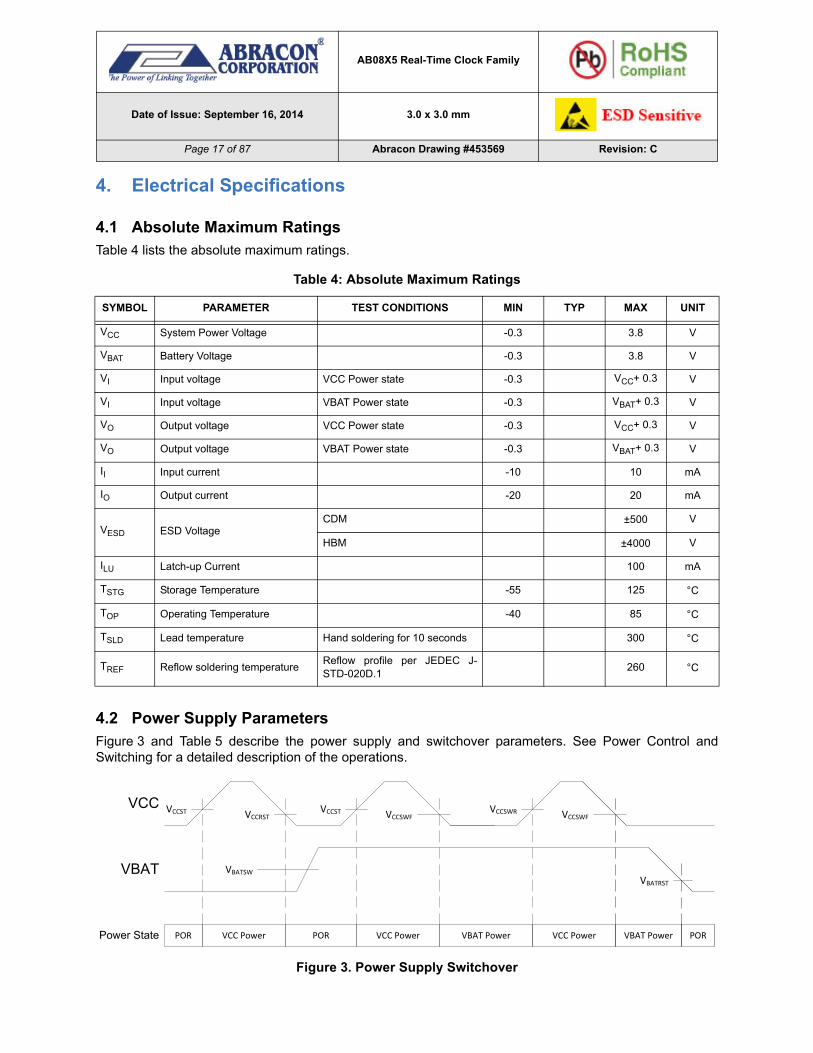
4.2 Power Supply ParametersFigure 3 and Table 5 describe the power supply and switchover parameters. See Power Control andSwitching for a detailed description of the operations.
Figure 3. Power Supply Switchover
Table 4: Absolute Maximum Ratings
SYMBOL PARAMETER TEST CONDITIONS MIN TYP MAX UNIT
VCC System Power Voltage -0.3 3.8 V
VBAT Battery Voltage -0.3 3.8 V
VI Input voltage VCC Power state -0.3 VCC+ 0.3 V
VI Input voltage VBAT Power state -0.3 VBAT+ 0.3 V
VO Output voltage VCC Power state -0.3 VCC+ 0.3 V
VO Output voltage VBAT Power state -0.3 VBAT+ 0.3 V
II Input current -10 10 mA
IO Output current -20 20 mA
VESD ESD VoltageCDM ±500 V
HBM ±4000 V
ILU Latch-up Current 100 mA
TSTG Storage Temperature -55 125 °C
TOP Operating Temperature -40 85 °C
TSLD Lead temperature Hand soldering for 10 seconds 300 °C
TREF Reflow soldering temperatureReflow profile per JEDEC J-STD-020D.1
260 °C
VCC
VBAT
Power State POR
VCCST VCCRST
VCC Power
VCCST
POR
VCCSWF
VCC Power VBAT Power
VBATSW
VCCSWR
VCC Power
VCCSWF
VBATRST
VBAT Power POR

AB08X5 Real-Time Clock Family
Date of Issue: September 16, 2014 3.0 x 3.0 mm
Page 18 of 87 Abracon Drawing #453569 Revision: C
For Table 5, TA = -40 °C to 85 °C, TYP values at 25 °C.
Table 5: Power Supply and Switchover Parameters
SYMBOL
PARAMETER PWR TYPE POWER STATETEST
CONDITIONSMIN TYP MAX UNIT
VCC System Power Voltage VCC Static VCC PowerClocks operatingand RAM andregisters retained
1.5 3.6 V
VCCIOVCC I/O Interface Voltage
VCC Static VCC Power I2C or SPI opera-tion
1.5 3.6 V
VCCST VCC Start-up Voltage(1) VCC Rising POR -> VCC Power 1.6 V
VCCRST VCC Reset Voltage VCC Falling VCC Power -> PORVBAT < VBAT,MIN or
no VBAT1.3 1.5 V
VCCSWRVCC Rising Switch-overThreshold Voltage
VCC RisingVBAT Power -> VCC Power
VBAT ≥ VBATRST 1.6 1.7 V
VCCSWFVCC Falling Switch-overThreshold Voltage
VCC FallingVCC Power -> VBAT Power
VBAT ≥ VBATSW,MIN 1.2 1.5 V
VCCSWHVCC Switchover Thresh-
old Hysteresis(2) VCC Hyst.VCC Power <-> VBAT Power
70 mV
VCCFSVCC Falling Slew Rate
to switch to VBAT state(4) VCC FallingVCC Power -> VBAT Power
VCC < VCCSW,MAX 0.7 1.4 V/ms
VBAT Battery Voltage VBAT Static VBAT PowerClocks operatingand RAM and reg-isters retained
1.4 3.6 V
VBATSWBattery Switchover Volt-
age Range(5) VBAT StaticVCC Power -> VBAT Power
1.6 3.6 V
VBATRSTFalling Battery POR Volt-
age(7) VBAT FallingVBAT Power ->POR
VCC < VCCSWF 1.1 1.4 V
VBMRGVBAT Margin above
VCC(3) VBAT Static VBAT Power 200 mV
VBATESRVBAT supply series resis-
tance(6)VBAT Static VBAT Power 1.0 1.5 k
(1) VCC must be above VCCST to exit the POR state, independent of the VBAT voltage.(2) Difference between VCCSWR and VCCSWF.(3) VBAT must be higher than VCC by at least this voltage to ensure the AB08X5 remains in the VBAT Power state.(4) Maximum VCC falling slew rate to guarantee correct switchover to VBAT Power state. There is no VCC falling slew rate
requirement if switching to the VBAT power source is not required.(5) VBAT voltage to guarantee correct transition to VBAT Power state when VCC falls.(6) Total series resistance of the power source attached to the VBAT pin. The optimal value is 1.5k, which may require an
external resistor. VBAT power source ESR + external resistor value = 1.5k(7) VBATRST is also the static voltage required on VBAT for register data retention.

AB08X5 Real-Time Clock Family
Date of Issue: September 16, 2014 3.0 x 3.0 mm
Page 19 of 87 Abracon Drawing #453569 Revision: C
4.3 Operating ParametersTable 6 lists the operating parameters.
For Table 6, TA = -40 °C to 85 °C, TYP values at 25 °C.
Table 6: Operating Parameters
SYMBOL PARAMETERTEST
CONDITIONSVCC MIN TYP MAX UNIT
VT+Positive-going Input Thresh-old Voltage
3.0V 1.5 2.0V
1.8V 1.1 1.25
VT-Negative-going Input Thresh-old Voltage
3.0V 0.8 0.9V
1.8V 0.5 0.6
IILEAK Input leakage current 3.0V 0.02 80 nA
CI Input capacitance 3 pF
VOHHigh level output voltage onpush-pull outputs
1.7V – 3.6V 0.8•VCC V
VOL Low level output voltage 1.7V – 3.6V 0.2•VCC V
IOHHigh level output current onpush-pull outputs
VOH = 0.8VCC
1.7V -2 -3.8
mA1.8V -3 -4.3
3.0V -7 -11
3.6V -8.8 -15
IOL Low level output current VOL = 0.2VCC
1.7V 3.3 5.9
mA1.8V 6.1 6.9
3.0V 17 19
3.6V 18 20
IOLEAK Output leakage current 1.7V – 3.6V 0.02 80 nA

AB08X5 Real-Time Clock Family
Date of Issue: September 16, 2014 3.0 x 3.0 mm
Page 20 of 87 Abracon Drawing #453569 Revision: C
4.4 Oscillator Parameters
Table 7 lists the oscillator parameters.
For Table 7, TA = -40 °C to 85 °C unless otherwise indicated.VCC = 1.7 to 3.6V, TYP values at 25 °C and 3.0V.
Table 7: Oscillator Parameters
SYMBOL PARAMETER TEST CONDITIONS MIN TYP MAX UNIT
FXTXI and XO pin Crystal Fre-quency
32.768 kHz
FOFXT Oscillator failure detectionfrequency
8 kHz
CINXInternal XI and XO pin capac-itance
1 pF
CEXExternal XI and XO pin PCBcapacitance
1 pF
OAXT XT Oscillation AllowanceAt 25°C using a 32.768 kHzcrystal
270 320 kΩ
FRCCCalibrated RC Oscillator Fre-
quency(1)Factory Calibrated at 25°C,VCC = 2.8V
128 Hz
FRCUUncalibrated RC OscillatorFrequency
Calibration Disabled (OFF-SETR = 0)
89 122 220 Hz
JRCCCRC Oscillator cycle-to-cyclejitter
Calibration Disabled (OFF-SETR = 0) – 128 Hz
2000
ppmCalibration Disabled (OFF-SETR = 0) – 1 Hz
500
AXTXT mode digital calibration
accuracy(1)Calibrated at an initial tem-perature and voltage
-2 2 ppm
AAC
Autocalibration mode timingaccuracy, 512 second period,
TA = -10°C to 60°C(1)
24 hour run time 35
ppm1 week run time 20
1 month run time 10
1 year run time 3
TACAutocalibration mode operat-
ing temperature(2) -10 60 °C
(1) Timing accuracy is specified at 25°C after digital calibration of the internal RC oscillator and 32.768 kHz crystal. A typical 32.768 kHz tuning fork crystal has a negative temperature coefficient with a parabolic frequency deviation, which due to the crystal alone can result in a change of up to 150 ppm across the entire operating temperature range of -40°C to 85°C in XT mode. Autocalibration mode timing accuracy is specified relative to XT mode timing accuracy from -10°C to 60°C.
(2) Outside of this temperature range, the RC oscillator frequency change due to temperature may be outside of the allowable RC digital calibration range (+/-12%) for autocalibration mode.If this happens, an autocalibration failure will occur and the ACF interrupt flag is set. The AB08X5 should be switched to use the XT oscillator as its clock source. Please see the Autocalibration Fail section for more details.

AB08X5 Real-Time Clock Family
Date of Issue: September 16, 2014 3.0 x 3.0 mm
Page 21 of 87 Abracon Drawing #453569 Revision: C
Figure 4 shows the typical calibrated RC oscillator frequency variation vs. temperature. RC oscillatorcalibrated at 2.8V, 25°C.
Figure 4. Calibrated RC Oscillator Typical Frequency Variation vs. Temperature
Figure 5 shows the typical uncalibrated RC oscillator frequency variation vs. temperature.
Figure 5. Uncalibrated RC Oscillator Typical Frequency Variation vs. Temperature
115
120
125
130
135
140
145
150
‐40 ‐30 ‐20 ‐10 0 10 20 30 40 50 60 70 80
RC Frequency (Hz)
Temperature (°C)
VCC = 1.8V
VCC = 3.0V
TA = 25 °C
115
120
125
130
135
140
145
‐40 ‐30 ‐20 ‐10 0 10 20 30 40 50 60 70 80
RC Frequency (Hz)
Temperature (°C)
VCC = 1.8V
VCC = 3.0V
TA = 25 °C

AB08X5 Real-Time Clock Family
Date of Issue: September 16, 2014 3.0 x 3.0 mm
Page 22 of 87 Abracon Drawing #453569 Revision: C
4.5 VCC Supply Current
Table 8 lists the current supplied into the VCC power input under various conditions.
For Table 8, TA = -40 °C to 85 °C, VBAT = 0 V to 3.6 VTYP values at 25 °C, MAX values at 85 °C, VCC Power state
Table 8: VCC Supply Current
SYMBOL PARAMETER TEST CONDITIONS VCC MIN TYP MAX UNIT
IVCC:I2CVCC supply current during I2C
burst read/write
400kHz bus speed, 2.2k pull-up
resistors on SCL/SDA(1)
3.0V 6 10µA
1.8V 1.5 3
IVCC:SPIWVCC supply current during SPI
burst write2 MHz bus speed (2)
3.0V 8 12µA
1.8V 4 6
IVCC:SPIRVCC supply current during SPI
burst read2 MHz bus speed (2)
3.0V 23 37µA
1.8V 13 21
IVCC:XTVCC supply current in XT oscil-
lator mode
Time keeping mode with XT
oscillator running(3)
3.0V 55 330nA
1.8V 51 290
IVCC:RCVCC supply current in RC oscil-
lator mode
Time keeping mode with onlythe RC oscillator running (XT
oscillator is off)(3)
3.0V 14 220nA
1.8V 11 170
IVCC:ACAL
Average VCC supply current in
Autocalibrated RC oscillatormode
Time keeping mode with onlyRC oscillator running and Auto-calibration enabled. ACP =
512 seconds(3)
3.0V 22 235
nA1.8V 18 190
(1) Excluding external peripherals and pull-up resistor current. All other inputs (besides SDA and SCL) are at 0V or VCC.
AB0805 only. Test conditions: Continuous burst read/write, 0x55 data pattern, 25 s between each data byte, 20 pF load on each bus pin.
(2) Excluding external peripheral current. All other inputs (besides SDI, nCE and SCL) are at 0V or VCC. AB0815 only. Test
conditions: Continuous burst write, 0x55 data pattern, 25 s between each data byte, 20 pF load on each bus pin.(3) All inputs and outputs are at 0 V or VCC

AB08X5 Real-Time Clock Family
Date of Issue: September 16, 2014 3.0 x 3.0 mm
Page 23 of 87 Abracon Drawing #453569 Revision: C
Figure 6 shows the typical VCC power state operating current vs. temperature in XT mode.
Figure 6. Typical VCC Current vs. Temperature in XT Mode
Figure 7 shows the typical VCC power state operating current vs. temperature in RC mode.
Figure 7. Typical VCC Current vs. Temperature in RC Mode
40
50
60
70
80
90
100
110
120
130
‐40 ‐30 ‐20 ‐10 0 10 20 30 40 50 60 70 80
VCC Power State, XT Mode Current (nA)
Temperature (°C)
VCC = 1.8V
VCC = 3.0V
TA = 25 °C
5
15
25
35
45
55
65
75
‐40 ‐30 ‐20 ‐10 0 10 20 30 40 50 60 70 80
VCC Power State, RC M
ode Current (nA)
Temperature (°C)
VCC = 1.8V
VCC = 3.0V
TA = 25 °C
AB08X5 Real-Time Clock Family
Date of Issue: September 16, 2014 3.0 x 3.0 mm
Page 24 of 87 Abracon Drawing #453569 Revision: C
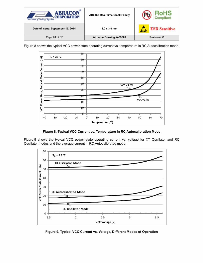
Figure 8 shows the typical VCC power state operating current vs. temperature in RC Autocalibration mode.
Figure 8. Typical VCC Current vs. Temperature in RC Autocalibration Mode
Figure 9 shows the typical VCC power state operating current vs. voltage for XT Oscillator and RCOscillator modes and the average current in RC Autocalibrated mode.
Figure 9. Typical VCC Current vs. Voltage, Different Modes of Operation
5
10
15
20
25
30
35
40
45
50
55
‐40 ‐30 ‐20 ‐10 0 10 20 30 40 50 60 70
VCC
Pow
er State, A
utocal Mode Current (nA)
Temperature (°C)
VCC = 1.8V
VCC = 3.0V
TA = 25 °C
0
10
20
30
40
50
60
70
1.5 2 2.5 3 3.5
VCC
Pow
er State
Current (nA)
VCC Voltage (V)
RC Oscillator Mode
XT Oscillator Mode
RC Autocalibrated Mode
TA = 25 °C

AB08X5 Real-Time Clock Family
Date of Issue: September 16, 2014 3.0 x 3.0 mm
Page 25 of 87 Abracon Drawing #453569 Revision: C
Figure 10 shows the typical VCC power state operating current during continuous I2C and SPI burst readand write activity. Test conditions: TA = 25 °C, 0x55 data pattern, 25 s between each data byte, 20 pFload on each bus pin, pull-up resistor current not included.
Figure 10. Typical VCC Current vs. Voltage, I²C and SPI Burst Read/Write
0
5
10
15
20
25
30
1.8 2 2.2 2.4 2.6 2.8 3 3.2 3.4 3.6
VCC Current (µA)
VCC Voltage (V)
I2C Burst Read/Write
SPI Burst Read
SPI Burst Write
TA = 25 °C

AB08X5 Real-Time Clock Family
Date of Issue: September 16, 2014 3.0 x 3.0 mm
Page 26 of 87 Abracon Drawing #453569 Revision: C
4.6 VBAT Supply CurrentTable 9 lists the current supplied into the VBAT power input under various conditions.
Figure 11 shows the typical VBAT power state operating current vs. temperature in XT mode.
Figure 11. Typical VBAT Current vs. Temperature in XT Mode
For Table 9, TA = -40 °C to 85 °C, TYP values at 25 °C, MAX values at 85 °C, VBAT Power state.
Table 9: VBAT Supply Current
SYMBOL PARAMETER TEST CONDITIONS VCC VBAT MIN TYP MAX UNIT
IVBAT:XTVBAT supply current inXT oscillator mode
Time keeping mode with
XT oscillator running(1)< VCCSWF
3.0V 56 330nA
1.8V 52 290
IVBAT:RCVBAT supply current inRC oscillator mode
Time keeping mode withonly the RC oscillator run-
ning (XT oscillator is off)(1)< VCCSWF
3.0V 16 220nA
1.8V 12 170
IVBAT:ACAL
Average VBAT supplycurrent in AutocalibratedRC oscillator mode
Time keeping mode withthe RC oscillator running.Autocalibration enabled.
ACP = 512 seconds(1)
< VCCSWF
3.0V 24 235
nA1.8V 20 190
IVBAT:VCCVBAT supply current inVCC powered mode
VCC powered mode(1) 1.7 - 3.6 V3.0V -5 0.6 20
nA1.8V -10 0.5 16
(1) Test conditions: All inputs and outputs are at 0 V or VCC.
40
50
60
70
80
90
100
110
120
130
‐40 ‐30 ‐20 ‐10 0 10 20 30 40 50 60 70 80
VBAT Power State, XT Mode Current (nA)
Temperature (°C)
VBAT = 1.8V
VBAT= 3.0V
TA = 25 °C

AB08X5 Real-Time Clock Family
Date of Issue: September 16, 2014 3.0 x 3.0 mm
Page 27 of 87 Abracon Drawing #453569 Revision: C
Figure 12 shows the typical VBAT power state operating current vs. temperature in RC mode.
Figure 12. Typical VBAT Current vs. Temperature in RC Mode
Figure 13 shows the typical VBAT power state operating current vs. temperature in RC Autocalibrationmode.
Figure 13. Typical VBAT Current vs. Temperature in RC Autocalibration Mode
5
15
25
35
45
55
65
75
‐40 ‐30 ‐20 ‐10 0 10 20 30 40 50 60 70 80
VBAT Power State, RC Mode Current (nA)
Temperature (°C)
VBAT= 1.8V
VBAT= 3.0V
TA = 25 °C
5
10
15
20
25
30
35
40
45
50
55
‐40 ‐30 ‐20 ‐10 0 10 20 30 40 50 60 70
VBAT Pow
er State, Autocal M
ode
Current (nA
)
Temperature (°C)
VBAT= 1.8V
VBAT= 3.0V
TA = 25 °C
AB08X5 Real-Time Clock Family
Date of Issue: September 16, 2014 3.0 x 3.0 mm
Page 28 of 87 Abracon Drawing #453569 Revision: C
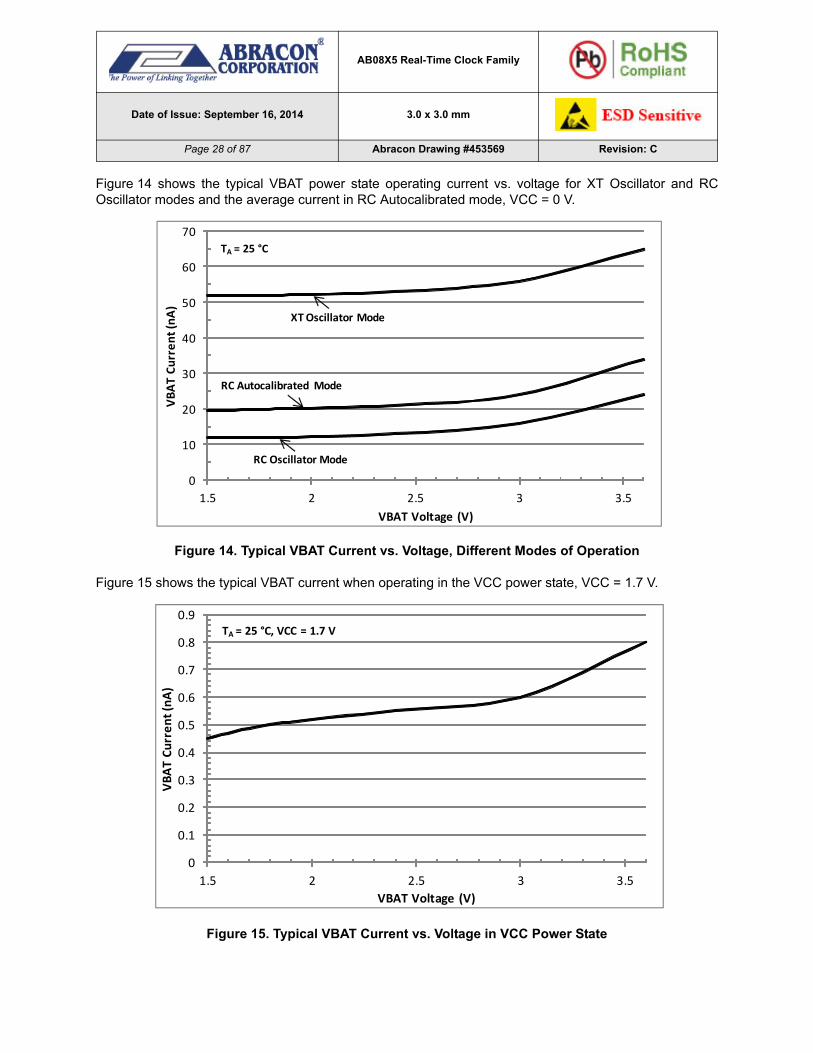
Figure 14 shows the typical VBAT power state operating current vs. voltage for XT Oscillator and RCOscillator modes and the average current in RC Autocalibrated mode, VCC = 0 V.
Figure 14. Typical VBAT Current vs. Voltage, Different Modes of Operation
Figure 15 shows the typical VBAT current when operating in the VCC power state, VCC = 1.7 V.
Figure 15. Typical VBAT Current vs. Voltage in VCC Power State
0
10
20
30
40
50
60
70
1.5 2 2.5 3 3.5
VBAT Current (nA)
VBAT Voltage (V)
RC Oscillator Mode
XT Oscillator Mode
RC Autocalibrated Mode
TA = 25 °C
0
0.1
0.2
0.3
0.4
0.5
0.6
0.7
0.8
0.9
1.5 2 2.5 3 3.5
VBAT Current (nA)
VBAT Voltage (V)
TA = 25 °C, VCC = 1.7 V

AB08X5 Real-Time Clock Family
Date of Issue: September 16, 2014 3.0 x 3.0 mm
Page 29 of 87 Abracon Drawing #453569 Revision: C
4.7 BREF Electrical CharacteristicsTable 10 lists the parameters of the VBAT voltage thresholds. BREF values other than those listed in thetable are not supported.
For Table 10, TA = -20 °C to 70 °C, TYP values at 25 °C, VCC = 1.7 to 3.6V.
Table 10: BREF Parameters
SYMBOL PARAMETER BREF MIN TYP MAX UNIT
VBRF VBAT falling threshold
0111 2.3 2.5 3.3
V1011 1.9 2.1 2.8
1101 1.6 1.8 2.5
1111 1.4
VBRR VBAT rising threshold
0111 2.6 3.0 3.4
V1011 2.1 2.5 2.9
1101 1.9 2.2 2.7
1111 1.6
VBRH VBAT threshold hysteresis
0111 0.5
V1011 0.4
1101 0.4
1111 0.2
TBRVBAT analog comparator recom-mended operating temperature range
All values -20 70 °C

AB08X5 Real-Time Clock Family
Date of Issue: September 16, 2014 3.0 x 3.0 mm
Page 30 of 87 Abracon Drawing #453569 Revision: C
4.8 I²C AC Electrical Characteristics
Figure 16 and Table 11 describe the I2C AC electrical parameters.
Figure 16. I²C AC Parameter Definitions
For Table 11, TA = -40 °C to 85 °C, TYP values at 25 °C.
Table 11: I²C AC Electrical Parameters
SYMBOL PARAMETER VCC MIN TYP MAX UNIT
fSCL SCL input clock frequency 1.7V-3.6V 10 400 kHz
tLOW Low period of SCL clock 1.7V-3.6V 1.3 µs
tHIGH High period of SCL clock 1.7V-3.6V 600 ns
tRISE Rise time of SDA and SCL 1.7V-3.6V 300 ns
tFALL Fall time of SDA and SCL 1.7V-3.6V 300 ns
tHD:STA START condition hold time 1.7V-3.6V 600 ns
tSU:STA START condition setup time 1.7V-3.6V 600 ns
tSU:DAT SDA setup time 1.7V-3.6V 100 ns
tHD:DAT SDA hold time 1.7V-3.6V 0 ns
tSU:STO STOP condition setup time 1.7V-3.6V 600 ns
tBUF Bus free time before a new transmission 1.7V-3.6V 1.3 µs
tBUF
SCL
SDA
tHD:STA
tLOW
tRISE
SDA tSU:STA
tHD:DAT
tHIGH
tSU:DAT
tSU:STO
tFALL
AB08X5 Real-Time Clock Family
Date of Issue: September 16, 2014 3.0 x 3.0 mm
Page 31 of 87 Abracon Drawing #453569 Revision: C
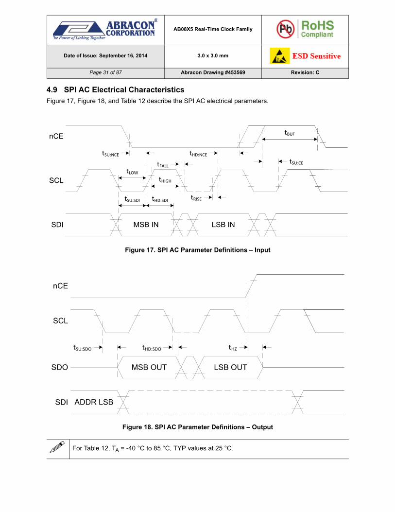
4.9 SPI AC Electrical CharacteristicsFigure 17, Figure 18, and Table 12 describe the SPI AC electrical parameters.
Figure 17. SPI AC Parameter Definitions – Input
Figure 18. SPI AC Parameter Definitions – Output
For Table 12, TA = -40 °C to 85 °C, TYP values at 25 °C.
SCL tHIGH
tLOW
nCE
tSU:NCE
SDI
tSU:SDI tHD:SDI
MSB IN LSB IN
tRISE
tFALL
tHD:NCEtSU:CE
tBUF
SCL
nCE
SDI
tHD:SDOtSU:SDO
SDO
ADDR LSB
MSB OUT LSB OUT
tHZ

AB08X5 Real-Time Clock Family
Date of Issue: September 16, 2014 3.0 x 3.0 mm
Page 32 of 87 Abracon Drawing #453569 Revision: C
Table 12: SPI AC Electrical Parameters
SYMBOL PARAMETER VCC MIN TYP MAX UNIT
fSCL SCL input clock frequency 1.7V–3.6V 0.01 2 MHz
tLOW Low period of SCL clock 1.7V–3.6V 200 ns
tHIGH High period of SCL clock 1.7V–3.6V 200 ns
tRISE Rise time of all signals 1.7V–3.6V 1 µs
tFALL Fall time of all signals 1.7V–3.6V 1 µs
tSU:NCE nCE low setup time to SCL 1.7V–3.6V 200 ns
tHD:NCE nCE hold time to SCL 1.7V–3.6V 200 ns
tSU:CE nCE high setup time to SCL 1.7V–3.6V 200 ns
tSU:SDI SDI setup time 1.7V–3.6V 40 ns
tHD:SDI SDI hold time 1.7V–3.6V 50 ns
tSU:SDO SDO output delay from SCL 1.7V–3.6V 150 ns
tHD:SDO SDO output hold from SCL 1.7V–3.6V 0 ns
tHZ SDO output Hi-Z from nCE 1.7V–3.6V 250 ns
tBUF nCE high time before a new transmission 1.7V–3.6V 200 ns
AB08X5 Real-Time Clock Family
Date of Issue: September 16, 2014 3.0 x 3.0 mm
Page 33 of 87 Abracon Drawing #453569 Revision: C
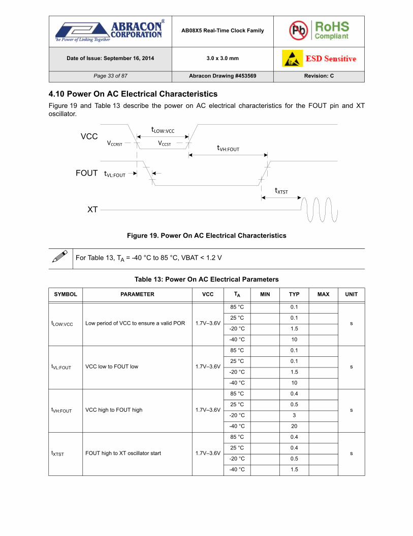
4.10 Power On AC Electrical CharacteristicsFigure 19 and Table 13 describe the power on AC electrical characteristics for the FOUT pin and XToscillator.
Figure 19. Power On AC Electrical Characteristics
For Table 13, TA = -40 °C to 85 °C, VBAT < 1.2 V
Table 13: Power On AC Electrical Parameters
SYMBOL PARAMETER VCC TA MIN TYP MAX UNIT
tLOW:VCC Low period of VCC to ensure a valid POR 1.7V–3.6V
85 °C 0.1
s25 °C 0.1
-20 °C 1.5
-40 °C 10
tVL:FOUT VCC low to FOUT low 1.7V–3.6V
85 °C 0.1
s25 °C 0.1
-20 °C 1.5
-40 °C 10
tVH:FOUT VCC high to FOUT high 1.7V–3.6V
85 °C 0.4
s25 °C 0.5
-20 °C 3
-40 °C 20
tXTST FOUT high to XT oscillator start 1.7V–3.6V
85 °C 0.4
s25 °C 0.4
-20 °C 0.5
-40 °C 1.5
VCC
FOUT tVL:FOUT
tLOW:VCC
tVH:FOUTVCCRST VCCST
XT
tXTST

AB08X5 Real-Time Clock Family
Date of Issue: September 16, 2014 3.0 x 3.0 mm
Page 34 of 87 Abracon Drawing #453569 Revision: C
5. Functional Description
Figure 20 illustrates the AB08X5 functional design.
Figure 20. Detailed Block Diagram
The AB08X5 serves as a full function RTC for host processors such as microcontrollers. The AB08X5includes 3 distinct feature groups: 1) baseline timekeeping features, 2) advanced timekeeping features,and 3) basic power management features. Functions from each feature group may be controlled via I/O
offset mapped registers. These registers are accessed using either an I2C serial interface (e.g., in theAB0805) or a SPI serial interface (e.g., in the AB0815). Each feature group is described briefly below andin greater detail in subsequent sections.
The baseline timekeeping feature group supports the standard 32.786 kHz crystal (XT) oscillation mode formaximum frequency accuracy with an ultra-low current draw of 55 nA. The baseline timekeeping featuregroup also includes a standard set of counters monitoring hundredths of a second up through centuries. Acomplement of countdown timers and alarms may additionally be set to initiate interrupts or resets onseveral of the outputs.
XT Osc
RC Osc
Divider
Seconds
Minutes
Hours
Days
Weekdays
Months
Years
Power Control
VCC VBAT
I2C/SPI InterfaceSCL
SDA/O
Control
Alarms
Int/Clock
FOUT/nIRQnIRQ2
VSS
SDInCE
WDIRAM
XO
XI
nTIRQ
Timer
WDT
100ths
Divider
Calibration Engine
EXTI
AnalogCompare

AB08X5 Real-Time Clock Family
Date of Issue: September 16, 2014 3.0 x 3.0 mm
Page 35 of 87 Abracon Drawing #453569 Revision: C
The advanced timekeeping feature group supports two additional oscillation modes: 1) RC oscillator mode,and 2) Autocalibration mode. At only 14 nA, the temperature-compensated RC oscillator mode provides aneven lower current draw than the XT oscillator for applications with reduced frequency accuracyrequirements. A proprietary calibration algorithm allows the AB08X5 to digitally tune the RC oscillatorfrequency and the XT oscillator frequency with accuracy as low as 2 ppm at a given temperature. InAutocalibration mode, the RC oscillator is used as the primary oscillation source and is periodicallycalibrated against the XT oscillator. Autocalibration may be done automatically every 8.5 minutes or 17minutes and may also be initiated via software. This mode enables average current draw of only 22 nAwith frequency accuracy similar to the XT oscillator. The advanced timekeeping feature group alsoincludes a rich set of input and output configuration options that enables the monitoring of externalinterrupts (e.g., pushbutton signals), the generation of clock outputs, and watchdog timer functionality.
Power management features built into the AB08X5 enable it to operate as a backup device in both line-powered and battery-powered systems. An integrated power control module automatically detects whenmain power (VCC) falls below a threshold and switches to backup power (VBAT). 256B of ultra-lowleakage RAM enable the storage of key parameters when operating on backup power. The AB08X5 alsoincludes digitally-tunable voltage detection on the backup power supply.
Each functional block is explained in detail in the remainder of this section. The functional descriptionsrefer to the registers shown in the Register Definitions (0x00 to 0x0F) and Register Definitions (0x10 to0xFF) tables. A detailed description of all registers can be found in the Registers section of this document.
5.1 I²C Interface
The AB08X5 includes a standard I2C interface. The device is accessed at addresses 0xD2/D3, and
supports Fast Mode (up to 400 kHz). The I2C interface consists of two lines: one bi-directional data line(SDA) and one clock line (SCL). Both the SDA and the SCL lines must be connected to a positive supplyvoltage via a pull-up resistor. By definition, a device that sends a message is called the “transmitter”, andthe device that accepts the message is called the “receiver”. The device that controls the message transferby driving SCL is called “master”. The devices that are controlled by the master are called “slaves”. TheAB08X5 is always a slave device.
I2C termination resistors should be above 2.2 kΩ, and for systems with short I2C bus wires/traces and fewconnections these terminators can typically be as large as 22 kΩ (for 400 kHz operation) or 56 kΩ (for 100kHz operation). Larger resistors will produce lower system current consumption.
The following protocol has been defined:
• Data transfer may be initiated only when the bus is not busy.• During data transfer, the data line must remain stable whenever the clock line is high.• Changes in the data line while the clock line is high will be interpreted as control signals.
A number of bus conditions have been defined (see Figure 21) and are described in the following sections.
Figure 21. Basic I²C Conditions
SDA
SCL
START SDA Stable
SDA may change
STOP
Not Busy

AB08X5 Real-Time Clock Family
Date of Issue: September 16, 2014 3.0 x 3.0 mm
Page 36 of 87 Abracon Drawing #453569 Revision: C
5.1.1 Bus Not Busy
Both SDA and SCL remain high.
5.1.2 Start Data Transfer
A change in the state of SDA from high to low, while SCL is high, defines the START condition. A STARTcondition which occurs after a previous START but before a STOP is called a RESTART condition, andfunctions exactly like a normal STOP followed by a normal START.
5.1.3 Stop Data Transfer
A change in the state of SDA from low to high, while SCL is high, defines the STOP condition.
5.1.4 Data Valid
After a START condition, SDA is stable for the duration of the high period of SCL. The data on SDA may bechanged during the low period of SCL. There is one clock pulse per bit of data. Each data transfer isinitiated with a START condition and terminated with a STOP condition. The number of data bytestransferred between the START and STOP conditions is not limited. The information is transmitted byte-wide and each receiver acknowledges with a ninth bit.
5.1.5 Acknowledge
Each byte of eight bits is followed by one acknowledge (ACK) bit as shown in Figure 22. This acknowledgebit is a low level driven onto SDA by the receiver, whereas the master generates an extra acknowledgerelated SCL pulse. A slave receiver which is addressed is obliged to generate an acknowledge after thereception of each byte. Also, on a read transfer a master receiver must generate an acknowledge after thereception of each byte that has been clocked out of the slave transmitter. The device that acknowledgesmust pull down the SDA line during the acknowledge clock pulse in such a way that the SDA line is astable low during the high period of the acknowledge related SCL pulse. A master receiver must signal anend-of-data to the slave transmitter by not generating an acknowledge (a NAK) on the last byte that hasbeen clocked out of the slave. In this case, the transmitter must leave the data line high to enable themaster to generate the STOP condition.
Figure 22. I²C Acknowledge Address Operation
Figure 23 illustrates the operation with which the master addresses the AB08X5. After the STARTcondition, a 7-bit address is transmitted MSB first. If this address is 0b1101001 (0xD2/3), the AB08X5 isselected, the eighth bit indicate a write (RW = 0) or a read (RW = 1) operation and the AB08X5 suppliesthe ACK. The AB08X5 ignores all other address values and does not respond with an ACK.
SDA
SCL
START
MSB (bit 7) Bit 6 Bit 0 ACK
1 2 8 9

AB08X5 Real-Time Clock Family
Date of Issue: September 16, 2014 3.0 x 3.0 mm
Page 37 of 87 Abracon Drawing #453569 Revision: C
Figure 23. I²C Address Operation
5.1.6 Offset Address Transmission
If the RW bit of the Address Operation indicates a write, the next byte transmitted from the master is theOffset Address as shown in Figure 24. This value is loaded into the Address Pointer of the AB08X5.
Figure 24. I²C Offset Address Transmission
5.1.7 Write Operation
In a write operation the master transmitter transmits to the AB08X5 slave receiver. The Address Operationhas a RW value of 0, and the second byte contains the Offset Address as in Figure 24. The next byte iswritten to the register selected by the Address Pointer (which was loaded with the Offset Address) and theAddress Pointer is incremented. Subsequent transfers write bytes into successive registers until a STOPcondition is received, as shown in Figure 25.
Figure 25. I²C Write Operation
5.1.8 Read Operation
In a read operation, the master first executes an Offset Address Transmission to load the Address Pointerwith the desired Offset Address. A subsequent operation will again issue the address of the AB08X5 butwith the RW bit as a 1 indicating a read operation. Figure 26 illustrates this transaction beginning with aRESTART condition, although a STOP followed by a START may also be used. After the addressoperation, the slave becomes the transmitter and sends the register value from the location pointed to bythe Address Pointer, and the Address Pointer is incremented. Subsequent transactions producesuccessive register values, until the master receiver responds with a NAK and/or STOP or RESTART to
A1 1 0 1 0 0 0SDA
SCL
RW
A1 1 0 1 0 0 0SDA
SCL
0 A7 6 5 4 3 2 1 0
Offset Address
Addr OffsetSDA
SCL
7 0
Byte N
AW A A 7 0
Byte N+1
A 7 0
Byte N+2
A
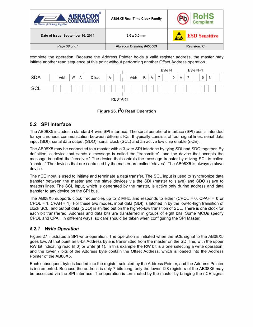
AB08X5 Real-Time Clock Family
Date of Issue: September 16, 2014 3.0 x 3.0 mm
Page 38 of 87 Abracon Drawing #453569 Revision: C
complete the operation. Because the Address Pointer holds a valid register address, the master mayinitiate another read sequence at this point without performing another Offset Address operation.
Figure 26. I²C Read Operation
5.2 SPI InterfaceThe AB08X5 includes a standard 4-wire SPI interface. The serial peripheral interface (SPI) bus is intendedfor synchronous communication between different ICs. It typically consists of four signal lines: serial datainput (SDI), serial data output (SDO), serial clock (SCL) and an active low chip enable (nCE).
The AB08X5 may be connected to a master with a 3-wire SPI interface by tying SDI and SDO together. Bydefinition, a device that sends a message is called the “transmitter”, and the device that accepts themessage is called the “receiver.” The device that controls the message transfer by driving SCL is called“master.” The devices that are controlled by the master are called “slaves”. The AB08X5 is always a slavedevice.
The nCE input is used to initiate and terminate a data transfer. The SCL input is used to synchronize datatransfer between the master and the slave devices via the SDI (master to slave) and SDO (slave tomaster) lines. The SCL input, which is generated by the master, is active only during address and datatransfer to any device on the SPI bus.
The AB08X5 supports clock frequencies up to 2 MHz, and responds to either (CPOL = 0, CPAH = 0 orCPOL = 1, CPAH = 1). For these two modes, input data (SDI) is latched in by the low-to-high transition ofclock SCL, and output data (SDO) is shifted out on the high-to-low transition of SCL. There is one clock foreach bit transferred. Address and data bits are transferred in groups of eight bits. Some MCUs specifyCPOL and CPAH in different ways, so care should be taken when configuring the SPI Master.
5.2.1 Write Operation
Figure 27 illustrates a SPI write operation. The operation is initiated when the nCE signal to the AB08X5goes low. At that point an 8-bit Address byte is transmitted from the master on the SDI line, with the upperRW bit indicating read (if 0) or write (if 1). In this example the RW bit is a one selecting a write operation,and the lower 7 bits of the Address byte contain the Offset Address, which is loaded into the AddressPointer of the AB08X5.
Each subsequent byte is loaded into the register selected by the Address Pointer, and the Address Pointeris incremented. Because the address is only 7 bits long, only the lower 128 registers of the AB08X5 maybe accessed via the SPI interface. The operation is terminated by the master by bringing the nCE signal
SDA
SCL
7 0
Byte N
A A 7 0
Byte N+1
NAddr AR
RESTART
Addr OffsetAW

AB08X5 Real-Time Clock Family
Date of Issue: September 16, 2014 3.0 x 3.0 mm
Page 39 of 87 Abracon Drawing #453569 Revision: C
high. Note that the SDO line is not used in a write operation and is held in the high impedance state by theAB08X5.
Figure 27. SPI Write Operation
5.2.2 Read Operation
Figure 28 illustrates a read operation. The address is transferred from the master to the slave just as it is ina write operation, but in this case the RW bit is a 0 indicating a read. After the transfer of the last addressbit, bit 0, the AB08X5 begins driving data from the register selected by the Address Pointer onto the SDOline, bit 7 first, and the Address Pointer is incremented. The transfer continues until the master brings thenCE line high.
Figure 28. SPI Read Operation
5.3 XT OscillatorThe AB08X5 includes a very power efficient crystal (XT) oscillator which runs at 32.786 kHz. This oscillatoris selected by setting the OSEL bit to 0 and includes a low jitter calibration function.
5.4 RC OscillatorThe AB08X5 includes an extremely low power RC oscillator which runs at 128 Hz. This oscillator isselected by setting the OSEL bit to 1. Switching between the XT and RC Oscillators is guaranteed toproduce less than one second of error in the Calendar Counters. The AB08X5 may be configured toautomatically switch to the RC Oscillator when VCC drops below its threshold by setting the AOS bit, and/or be configured to automatically switch if an XT Oscillator failure is detected by setting the FOS bit.
5.5 RTC Counter AccessWhen reading any of the counters in the RTC using a burst operation, the 1 Hz and 100 Hz clocks are heldoff during the access. This guarantees that a single burst will either read or write a consistent timer value(other than the Hundredths Counter – see Hundredths Synchronization). There is a watchdog function toensure that a very long pause on the interface does not cause the RTC to lose a clock.
W 6 5 4 3 2 1SDI
SCL
0 7 6 5 4 3 2 1 0
Offset Address
nCE
X
Data Byte N
7 6 5 4 3 2 1 0
Data Byte N+1
X
SDO
R 6 5 4 3 2 1SDI
SCL
0
Offset Address
nCE
X
Data Byte N Data Byte N+1
7 6 5 4 3 2 1 0 7 6 5 4 3 2 1 0SDO
X
AB08X5 Real-Time Clock Family
Date of Issue: September 16, 2014 3.0 x 3.0 mm
Page 40 of 87 Abracon Drawing #453569 Revision: C
On a write to any of the Calendar Counters, the entire timing chain up to 100 Hz (if the XT Oscillator isselected) or up to 1Hz (if the RC Oscillator is selected) is reset to 0. This guarantees that the Counters willbegin counting immediately after the write is complete, and that in the XT oscillator case the next 100 Hzclock will occur exactly 10 ms later. In the RC Oscillator case, the next 1 Hz clock will occur exactly 1second later. This allows a burst write to configure all of the Counters and initiate a precise time start. Notethat a Counter write may cause one cycle of a Square Wave output to be of an incorrect period.
The WRTC bit must be set in order to write to any of the Counter registers. This bit can be cleared toprevent inadvertent software access to the Counters.
5.6 Hundredths SynchronizationIf the Hundredths Counter is read as part of the burst read from the counter registers, the followingalgorithm must be used to guarantee correct read information.
1. Read the Counters, using a burst read. If the Hundredths Counter is neither 00 nor 99, the read is cor-rect.
2. If the Hundredths Counter was 00, perform the read again. The resulting value from this second readis guaranteed to be correct.
3. If the Hundredths Counter was 99, perform the read again.
A. If the Hundredths Counter is still 99, the results of the first read are guaranteed to be correct. Note that it is possible that the second read is not correct.
B. If the Hundredths Counter has rolled over to 00, and the Seconds Counter value from the sec-ond read is equal to the Seconds Counter value from the first read plus 1, both reads produced correct values. Alternatively, perform the read again. The resulting value from this third read is guaranteed to be correct.
C. If the Hundredths Counter has rolled over to 00, and the Seconds Counter value from the sec-ond read is equal to the Seconds Counter value from the first read, perform the read again. The resulting value from this third read is guaranteed to be correct.
5.7 Generating Hundredths of a SecondThe generation of an exact 100 Hz signal for the Hundredths Counter requires a special logic circuit. The2.048 kHz clock signal is divided by 21 for 12 iterations, and is alternately divided by 20 for 13 iterations.This produces an effective division of:
(21 * 12 + 20 * 13)/25 = 20.48
producing an exact long-term average 100 Hz output, with a maximum jitter of less than 1 ms. TheHundredths Counter is not available when the 128 Hz RC Oscillator is selected.
5.8 Watchdog TimerThe AB08X5 includes a Watchdog Timer (WDT), which can be configured to generate an interrupt or areset if it times out. The WDT is controlled by the Watchdog Timer Register (see 0x1B - Watchdog Timer).The RB field selects the frequency at which the timer is decremented, and the BMB field determines thevalue loaded into the timer when it is restarted. If the timer reaches a value of zero, the WDS bitdetermines whether an interrupt is generated in nIRQ. The timer reaching zero sets the WDT flag in theStatus Register, which may be cleared by setting the WDT flag to zero.
Two actions will restart the WDT timer:
1. Writing the Watchdog Timer Register with a new watchdog value.
2. A change in the level of the WDI pin.
AB08X5 Real-Time Clock Family
Date of Issue: September 16, 2014 3.0 x 3.0 mm
Page 41 of 87 Abracon Drawing #453569 Revision: C
If the Watchdog Timer generates an interrupt or reset, the Watchdog Timer Register must be written inorder to restart the Watchdog Timer function. If the BMB field is 0, the Watchdog Timer function is disabled.
The BMB field describes the maximum timeout delay. For example, if RB = 01 so that the clock period is250 ms, a BMB value of 9 implies that the timeout will occur between 2000 ms and 2250 ms after writingthe Watchdog Timer Register.
5.9 Digital Calibration
5.9.1 XT Oscillator Digital Calibration
In order to improve the accuracy of the XT oscillator, a Distributed Digital Calibration function is included(see 0x14 - Calibration XT). This function uses a calibration value, OFFSETX, to adjust the clock periodover a 16 second or 32 second calibration period. When the 32.786 kHz XT oscillator is selected, the clockat the 16.384 kHz level of the divider chain is modified on a selectable interval. Clock pulses are eitheradded or subtracted to ensure accuracy of the counters. If the CMDX bit is a 0 (normal calibration),OFFSETX cycles of the 16.384 kHz clock are gated (negative calibration) or replaced by 32.786 kHzpulses (positive calibration) within every 32 second calibration period. In this mode, each step in OFFSETXmodifies the clock frequency by 1.907 ppm, with a maximum adjustment of ~+120/-122 ppm. If the CMDXbit is 1 (coarse calibration), OFFSETX cycles of the 16.384 kHz clock are gated or replaced by the 32.786kHz clock within every 16 second calibration period. In this mode, each step in OFFSETX modifies theclock frequency by 3.814 ppm, with a maximum adjustment of ~+240/-244 ppm. OFFSETX contains atwo's complement value, so the possible steps are from -64 to +63. Note that unlike other implementations,Distributed Digital Calibration guarantees that the clock is precisely calibrated every 32 seconds withnormal calibration and every 16 seconds when coarse calibration is selected.
In addition to the normal calibration, the AB08X5 also includes an Extended Calibration field tocompensate for low capacitance environments. The frequency generated by the Crystal Oscillator may beslowed by 122 ppm times the value in the XTCAL (see 0x1D – Oscillator Status Register) field (0, -122,-244 or -366 ppm). The clock is still precisely calibrated in 16 or 32 seconds. The pulses which are added toor subtracted from the 16.384 kHz clock are spread evenly over each 16 or 32 second period using theAmbiq Micro patented Distributed Calibration algorithm. This ensures that in XT mode the maximum cycle-to-cycle jitter in any clock of a frequency 16.384 kHz or lower caused by calibration will be no more thanone 16.384 kHz period. This maximum jitter applies to all clocks in the AB08X5, including the CalendarCounter, Countdown Timer and Watchdog Timer clocks and any clock driven onto a clock output pin.
The XT oscillator calibration value is determined by the following process:
1. Set the OFFSETX, CMDX and XTCAL register fields to 0 to ensure calibration is not occurring.
2. Select the XT oscillator by setting the OSEL bit to 0.
3. Configure a 32768 Hz frequency square wave output on one of the output pins.
4. Precisely measure the exact frequency, Fmeas, at the output pin in Hz.
5. Compute the adjustment value required in ppm as ((32768 – Fmeas)*1000000)/32768 = PAdj
6. Compute the adjustment value in steps as PAdj/(1000000/2^19) = PAdj/(1.90735) = Adj
7. If Adj < -320, the XT frequency is too high to be calibrated
8. Else if Adj < -256, set XTCAL = 3, CMDX = 1, OFFSETX = (Adj +192)/2
9. Else if Adj < -192, set XTCAL = 3, CMDX = 0, OFFSETX = Adj +192
10. Else if Adj < -128, set XTCAL = 2, CMDX = 0, OFFSETX = Adj +128
11. Else if Adj < -64, set XTCAL = 1, CMDX = 0, OFFSETX = Adj + 64
12. Else if Adj < 64, set XTCAL = 0, CMDX = 0, OFFSETX = Adj
13. Else if Adj < 128, set XTCAL = 0, CMDX = 1, OFFSETX = Adj/2
14. Else the XT frequency is too low to be calibrated

AB08X5 Real-Time Clock Family
Date of Issue: September 16, 2014 3.0 x 3.0 mm
Page 42 of 87 Abracon Drawing #453569 Revision: C
5.9.2 RC Oscillator Digital Calibration
The RC Oscillator has a patented Distributed Digital Calibration function similar to that of the XT Oscillator(see 0x14 - Calibration XT). However, because the RC Oscillator has a greater fundamental variability, therange of calibration is much larger, with four calibration ranges selected by the CMDR field. When the 128Hz RC oscillator is selected, the clock at the 64 Hz level of the divider chain is modified on a selectableinterval using the calibration value OFFSETR. Clock pulses are either added or subtracted to ensureaccuracy of the counters. If the CMDR field is 00, OFFSETR cycles of the 64 Hz clock are gated (negativecalibration) or replaced by 128 Hz pulses (positive calibration) within every 8,192 second calibrationperiod. In this mode, each step in OFFSETR modifies the clock frequency by 1.907 ppm, with a maximumadjustment of +15,623/-15,625 ppm (+/- 1.56%). If the CMDR field is 01, OFFSETR cycles of the 64 Hzclock are gated or replaced by the 128 Hz clock within every 4,096 second calibration period. In this mode,each step in OFFSETR modifies the clock frequency by 3.82 ppm, with a maximum adjustment of +31,246/-31,250 ppm (+/-3.12%). If the CMDR field is 10, OFFSETR cycles of the 64 Hz clock are gated (negativecalibration) or replaced by 128 Hz pulses (positive calibration) within every 2,048 second calibrationperiod. In this mode, each step in OFFSETR modifies the clock frequency by 7.64 ppm, with a maximumadjustment of +62,492/-62,500 ppm (+/- 6.25%). If the CMDR field is 11, OFFSETR cycles of the 64 Hzclock are gated or replaced by the 128 Hz clock within every 1,024 second calibration period. In this mode,each step in OFFSETR modifies the clock frequency by 15.28 ppm, with a maximum adjustment of+124,984/-125,000 ppm (+/-12.5%). OFFSETR contains a two's complement value, so the possible stepsare from -8,192 to +8,191.
The pulses which are added to or subtracted from the 64 Hz clock are spread evenly over each 8,192second period using the Ambiq Micro patented Distributed Calibration algorithm. This ensures that in RCmode the maximum cycle-to-cycle jitter in any clock of a frequency 64 Hz or lower caused by calibrationwill be no more than one 64 Hz period. This maximum jitter applies to all clocks in the AB08X5 includingthe Calendar Counter, Countdown Timer and Watchdog Timer clocks and any clock driven onto a clockoutput pin.
The RC oscillator calibration value is determined by the following process:
1. Set the OFFSETR and CMDR register fields to 0 to ensure calibration is not occurring.
2. Select the RC oscillator by setting the OSEL bit to 1.
3. Configure a 128 Hz frequency square wave output on one of the output pins.
4. Precisely measure the exact frequency, Fmeas, at the output pin in Hz.
5. Compute the adjustment value required in ppm as ((128 – Fmeas)*1000000)/Fmeas = PAdj
6. Compute the adjustment value in steps as PAdj/(1000000/2^19) = PAdj/(1.90735) = Adj
7. If Adj < -65,536, the RC frequency is too high to be calibrated
8. Else if Adj < -32,768, set CMDR = 3, OFFSETR = Adj/8
9. Else if Adj < -16,384, set CMDR = 2, OFFSETR = Adj/4
10. Else if Adj < -8,192, set CMDR = 1, OFFSETR = Adj/2
11. Else if Adj < 8192, set CMDR = 0, OFFSETR = Adj
12. Else if Adj < 16,384, set CMDR = 1, OFFSETR = Adj/2
13. Else if Adj < 32,768, set CMDR = 2, OFFSETR = Adj/4
14. Else if Adj < 65,536, set CMDR = 3, OFFSETR = Adj/8
15. Else the RC frequency is too low to be calibrated
5.10 AutocalibrationThe AB08X5 includes a very powerful, patented automatic calibration feature, referred to asAutocalibration, which allows the RC Oscillator to be automatically calibrated to the XT Oscillator. The XTOscillator typically has much better stability than the RC Oscillator but the RC Oscillator requires

AB08X5 Real-Time Clock Family
Date of Issue: September 16, 2014 3.0 x 3.0 mm
Page 43 of 87 Abracon Drawing #453569 Revision: C
significantly less power. Autocalibration enables many system configurations to achieve accuracy andstability similar to that of the XT Oscillator while drawing current similar to that of the RC Oscillator.Autocalibration functions in two primary modes: XT Autocalibration Mode and RC Autocalibration Mode.See Abracon Application Note – AB08X5/AB18X5 Family Autocalibration for more details.
5.10.1 Autocalibration Operation
The Autocalibration operation counts the number of calibrated XT clock cycles within a specific period asdefined by the RC Oscillator and then loads new values into the Calibration RC Upper and RC Lowerregisters which will then adjust the RC Oscillator output to match the XT frequency.
5.10.2 XT Autocalibration Mode
In XT Autocalibration Mode, the OSEL register bit is 0 and the AB08X5 uses the XT Oscillator wheneverthe system power VCC is above the VCCSWF voltage. The RC Oscillator is periodically automaticallycalibrated to the XT Oscillator. If the AOS bit is set, when VCC drops below the VCCSWF threshold thesystem will switch to using VBAT, the clocks will begin using the RC Oscillator, Autocalibration will bedisabled and the XT Oscillator will be disabled to reduce power requirements. Because the RC Oscillatorhas been continuously calibrated to the XT Oscillator, it will be very accurate when the switch occurs.When VCC is again above the threshold, the system will switch back to use the XT Oscillator and restartAutocalibration.
5.10.3 RC Autocalibration Mode
In RC Autocalibration Mode, the OSEL register bit is 1 and the AB08X5 uses the RC Oscillator at all times.However, periodically the XT Oscillator is turned on and the RC Oscillator is calibrated to the XT Oscillator.This allows the system to operate most of the time with the XT Oscillator off but allow continuouscalibration of the RC Oscillator.
5.10.4 Autocalibration Frequency and Control
The Autocalibration function is controlled by the ACAL field in the Oscillator Control register as shown inTable 14. If ACAL is 00, no Autocalibration occurs. If ACAL is 10 or 11, Autocalibration occurs every 1024or 512 seconds, which is referred to as the Autocalibration Period (ACXP). In RC Autocalibration Mode, anAutocalibration operation results in the XT Oscillator being enabled for roughly 50 seconds. The 512second Autocalibration cycles have the XT Oscillator enabled approximately 10% of the time, while 1024second Autocalibration cycles have the XT Oscillator enabled approximately 4% of the time.
If ACAL is 00 and is then written with a different value, an Autocalibration cycle is immediately executed.This allows Autocalibration to be completely controlled by software. As an example, software could chooseto execute an Autocalibration cycle every 2 hours by keeping ACAL at 00, getting a two hour interruptusing the alarm function, generating an Autocalibration cycle by writing ACAL to 10 or 11, and thenreturning ACAL to 00.
Table 14: Autocalibration Modes
ACAL Value Calibration Mode
00 No Autocalibration
01 RESERVED
10 Autocalibrate every 1024seconds (~17minutes)
11 Autocalibrate every 512seconds (~9 minutes)

AB08X5 Real-Time Clock Family
Date of Issue: September 16, 2014 3.0 x 3.0 mm
Page 44 of 87 Abracon Drawing #453569 Revision: C
5.10.5 Autocalibration Filter (AF) Pin
In order to produce the optimal accuracy for the Autocalibrated RC Oscillator, a filter pin AF is provided. A47 pF capacitor should be connected between the AF pin and VSS. In order to enable the filter, the value0xA0 must be written to the AFCTRL Register at address 0x26(see 0x26 – AFCTRL). The AF filter isdisabled by writing 0x00 to the AFCTRL Register. No other values should be written to this register. TheConfiguration Key Register must be written with the value 0x9D immediately prior to writing the AFCTRLRegister.
If the filter capacitor is not connected to the AF pin or is not enabled, the RC Oscillator frequency willtypically be between 10 and 50 ppm slower than the XT Oscillator. If the capacitor is connected to the AFpin and enabled, the RC Oscillator frequency will be within the accuracy range specified in the OscillatorParameters table of the XT Oscillator.
5.10.6 Autocalibration Fail
If the operating temperature of the AB08X5 exceeds the Autocalibration range specified in the OscillatorParameters table or internal adjustment parameters are altered incorrectly, it is possible that the basicfrequency of the RC Oscillator is so far away from the nominal 128 Hz value (off by more than 12%) thatthe RC Calibration circuitry does not have enough range to correctly calibrate the RC Oscillator. If thissituation is detected during an Autocalibration operation, the ACF interrupt flag is set, an external interruptis generated if the ACIE register bit is set and the Calibration RC registers are not updated.
If an Autocalibration failure is detected while running in RC Autocalibration mode, it is advisable to switch into XT Autocalibration mode to maintain the timing accuracy. This is done by first ensuring a crystal oscillator failure has not occurred (OF flag = 0) and then clearing the OSEL bit. The ACAL field should remain set to either 11 (512 second period) or 10 (1024 second period). After the switch occurs, the OMODE bit is cleared.
While continuing to operate in XT Autocalibration mode, the following steps can be used to determine when it is safe to return to RC Autocalibration mode.
1. Clear the ACF flag and ACIE register bit.
2. Setup the Countdown Timer or Alarm to interrupt after the next Autocalibration cycle completes or lon-ger time period.
3. After the interrupt occurs, check the status of the ACF flag.
4. If the ACF flag is set, it is not safe to return to RC Autocalibration mode. Clear the ACF flag andrepeat steps 2-4.
5. If the ACF flag is still cleared, it is safe to return to RC Autocalibration mode by setting the OSEL bit.
As mentioned in the RC oscillator section, switching between XT and RC oscillators is guaranteed toproduce less than one second of error. However, this error needs to be considered and can be safelymanaged when implementing the steps above. For example, switching between oscillator modes every 48hours will produce less than 6 ppm of error.
5.11 Oscillator Failure DetectionIf the 32.786 kHz XT Oscillator generates clocks at less than 8 kHz for a period of more than 32 ms, theAB08X5 detects an Oscillator Failure. The Oscillator Failure function is controlled by several bits in theOscillator Control Register (see 0x1C Oscillator Control) and the Oscillator Status Register (see 0x1D -Oscillator Status Register). The OF flag is set when an Oscillator Failure occurs, and is also set when theinitially powers up. If the OFIE bit is set, the OF flag will generate an interrupt on IRQ.
If the FOS bit is set and the AB08X5 is currently using the XT Oscillator, it will automatically switch to theRC Oscillator on an Oscillator Failure. This guarantees that the system clock will not stop in any case. The

AB08X5 Real-Time Clock Family
Date of Issue: September 16, 2014 3.0 x 3.0 mm
Page 45 of 87 Abracon Drawing #453569 Revision: C
OMODE bit indicates the currently selected oscillator, which will not match the oscillator requested by theOSEL bit if the XT Oscillator is not running.
The OF flag will be set when the AB08X5 powers up, and will also be set whenever the XT Oscillator isstopped. This can happen when the STOP bit is set or the OSEL bit is set to 1 to select the RC Oscillator.Since the XT Oscillator is stopped in RC Autocalibration mode (see RC Autocalibration Mode), OF willalways be set in this mode. The OF flag should be cleared whenever the XT Oscillator is enabled prior toenabling the OF interrupt with OFIE.
5.12 InterruptsThe AB08X5 may generate a variety of interrupts which are ORed into the IRQ signal. This may be drivenonto either the FOUT/nIRQ pin or the nIRQ2 pin depending on the configuration of the OUT1S and OUT2Sfields (see 0x11 - Control2).
5.12.1 Interrupt Summary
The possible interrupts are summarized in Table 15. All enabled interrupts are ORed into the IRQ signalwhen their respective flags are set. Note that most interrupt outputs use the inverse of the interrupt (i.e.nIRQ). The fields are:
• Interrupt - the name of the specific interrupt.• Function - the functional area which generates the interrupt.• Enable - the register bit which enables the interrupt. Note that for the Watchdog interrupt, WDS is the
steering bit, so that the flag generates an interrupt if WDS is 0 and a reset if WDS is 1. In either case, the BMB field must be non-zero to generate the interrupt or reset.
• Pulse/Level - some interrupts may be configured to generate a pulse based on the register bits in this column. "Level Only" implies that only a level may be generated, and the interrupt will only go away when the flag is reset by software.
• Flag - the register bit which indicates that the function has occurred. Note that the flag being set will only generate an interrupt signal on an external pin if the corresponding interrupt enable bit is also set.
5.12.2 Alarm Interrupt AIRQ
The AB08X5 may be configured to generate the AIRQ interrupt when the values in the Time and DateRegisters match the values in the Alarm Registers. Which register comparisons are required to generateAIRQ is controlled by the RPT field as described in the Repeat Function table, allowing software to specifythe interrupt interval. When an Alarm Interrupt is generated, the ALM flag is set and an external interrupt is
Table 15: Interrupt Summary
Interrupt Function Enable Pulse/Level Flag
AIRQ Alarm Match AIE IM ALM
TIRQ Countdown Timer TIM TM TIM
WIRQ Watchdog !WDS Level Only WDT
BLIRQ Battery Low BLIE Level Only BL
X1IRQ External 1 EX1E Level Only EX1
X2IRQ External 2 EX2E Level Only EX2
OFIRQ Oscillator Fail OFIE Level Only OF
ACIRQ Autocal Fail ACIE Level Only ACF

AB08X5 Real-Time Clock Family
Date of Issue: September 16, 2014 3.0 x 3.0 mm
Page 46 of 87 Abracon Drawing #453569 Revision: C
generated based on the AIE bit and the pin configuration settings. The IM field controls the period of theexternal interrupt, including both level and pulse configurations.
5.12.3 Countdown Timer Interrupt TIRQ
The AB08X5 may be configured to generate the TIRQ interrupt when the Countdown Timer is enabled bythe TE bit and reaches the value of zero, which will set the TIM flag. The TM, TRPT and TFS fields controlthe interrupt timing (see 0x18 - Countdown Timer Control), and the TIE bit and the pin configurationsettings control external interrupt generation. The Timer interrupt is always driven onto the nTIRQ pin if it isavailable, and may also be driven onto a clock output pin by a configuration of the SQFS field (see 0x13 -SQW).
5.12.4 Watchdog Timer Interrupt WIRQ
The AB08X5 may be configured to generate the WIRQ interrupt when the Watchdog Timer reaches itstimeout value. This sets the WDT flag and is described in Watchdog Timer.
5.12.5 Battery Low Interrupt BLIRQ
The AB08X5 may be configured to generate the BLIRQ when the voltage on the VBAT pin crosses one ofthe thresholds set by the BREF field. The polarity of the detected crossing is set by the BPOL bit.
5.12.6 External Interrupts X1IRQ and X2IRQ
The AB08X5 may be configured to generate the X1IRQ and X2IRQ interrupts when the EXTI (X1IRQ) orWDI (X2IRQ) inputs toggle. The register bits EX1P and EX2P control whether the rising or fallingtransitions generate the respective interrupt. Changing EX1P or EX2P may cause an immediate interrupt,so the corresponding interrupt flag should be cleared after changing these bits.
The values of the EXTI and WDI pins may be directly read in the EXIN and WDIN register bits (see 0x3F -Extension RAM Address). By connecting an input such as a pushbutton to both EXTI and WDI, softwarecan debounce the switch input using software configurable delays.
5.12.7 Oscillator Fail Interrupt OFIRQ
The AB08X5 may be configured to generate the OFIRQ interrupt if the XT oscillator fails (see OscillatorFailure Detection).
5.12.8 Autocalibration Fail Interrupt ACIRQ
The AB08X5 may be configured to generate the ACIRQ interrupt if an Autocalibration operation fails (seeAutocalibration Fail).
5.12.9 Servicing Interrupts
When an interrupt is detected, software must clear the interrupt flag in order to prepare for a subsequentinterrupt. If only a single interrupt is enabled, software may simply write a zero to the correspondinginterrupt flag to clear the interrupt. However, because all of the flags in the Status register are written atonce, it is possible to clear an interrupt which has not been detected yet if multiple interrupts are enabled.The ARST register bit is provided to ensure that interrupts are not lost in this case. If ARST is a 1, a read ofthe Status register will produce the current state of all the interrupt flags and then clear them. An interruptoccurring at any time relative to this read is guaranteed to either produce a 1 on the Status read, or to setthe corresponding flag after the clear caused by the Status read. After servicing all interrupts whichproduced 1s in the read, software should read the Status register again until it returns all zeros in the flags,and service any interrupts with flags of 1.

AB08X5 Real-Time Clock Family
Date of Issue: September 16, 2014 3.0 x 3.0 mm
Page 47 of 87 Abracon Drawing #453569 Revision: C
Note that the OF and ACF interrupts are not handled with this process because they are in the OscillatorStatus register, but error interrupts are very rare and typically do not create any problems if the interruptsare cleared by writing the flag directly.
5.13 Power Control and SwitchingThe main power supply to the AB08X5 is the VCC pin, which operates over the range specified by theVCCIO parameter if there are I/O interface operations required, and the range specified by the VCC
parameter if only timekeeping operations are required. Some versions also include a backup supply whichis provided on the VBAT pin and must be in the range specified by the VBAT parameter in order to supplybattery power if VCC is below VCCSWF. Refer to the Power Supply and Switchover Parameters table for thespecifications related to the power supplies and switchover. There are several functions which are directlyrelated to the VBAT input. If a single power supply is used it must be connected to the VCC pin.
Figure 29 illustrates the various power states and the transitions between them. There are three powerstates:
1. POR – the power on reset state. If the AB08X5 is in this state, all registers including the Counter Reg-isters are initialized to their reset values.
2. VCC Power – the AB08X5 is powered from the VCC supply.
3. VBAT Power – the AB08X5 is powered from the VBAT supply.
Initially, VCC is below the VCCST voltage, VBAT is below the VBATSW voltage and the AB08X5 is in thePOR state. VCC rising above the VCCST voltage causes the AB08X5 to enter the VCC Power state. IfVBAT remains below VBATSW, VCC falling below the VCCRST voltage returns the AB08X5 to the POR state.
Figure 29. Power States
If VBAT rises above VBATSW in the POR state, the AB08X5 remains in the POR state. This allows theAB08X5 to be built into a module with a battery included, and minimal current will be drawn from thebattery until VCC is applied to the module the first time.
If the AB08X5 is in the VCC Power state and VBAT rises above VBATSW, the AB08X5 remains in the VCCPower state but automatic switchover becomes available. VBAT falling below VBATSW has no effect on thepower state as long as VCC remains above VCCSWF. If VCC falls below the VCCSWF voltage while VBAT isabove VBATSW the AB08X5 switches to the VBAT Power state. VCC rising above VCCSWR returns theAB08X5 to the VCC Power state. There is hysteresis in the rising and falling VCC thresholds to ensure thatthe AB08X5 does not switch back and forth between the supplies if VCC is near the thresholds. VCCSWF
and VCCSWR are independent of the VBAT voltage and allow the AB08X5 to minimize the current drawn
VCC
VBAT
Power State POR
VCCST VCCRST
VCC Power
VCCST
POR
VCCSWF
VCC Power VBAT Power
VBATSW
VCCSWR
VCC Power
VCCSWF
VBATRST
VBAT Power POR

AB08X5 Real-Time Clock Family
Date of Issue: September 16, 2014 3.0 x 3.0 mm
Page 48 of 87 Abracon Drawing #453569 Revision: C
from the VBAT supply by switching to VBAT only at the point where VCC is no longer able to power thedevice.
If the AB08X5 is in the VBAT Power state and VBAT falls below VBATRST, the AB08X5 will return to thePOR state.
Whenever the AB08X5 enters the VBAT Power state, the BAT flag in the Status Register (see 0x0F -Status (Read Only)) is set and may be polled by software. If the XT oscillator is selected and the AOS bit(see 0x1C - Oscillator Control) is set, the AB08X5 will automatically switch to the RC oscillator in the VBATPower state in order to conserve battery power. If the IOBM bit (see 0x27 – Batmode IO Register) is clear,
the I2C or SPI interface is disabled in the VBAT Power state in order to prevent erroneous accesses to theAB08X5 if the bus master loses power.
5.13.1 Battery Low Flag and Interrupt
If the VBAT voltage drops below the Falling Threshold selected by the BREF field (see 0x21 - BREFControl), the BL flag in the Status Register (see 0x0F - Status (Read Only)) is set. If the BLIE interruptenable bit (see 0x12 - Interrupt Mask) is set, the IRQ interrupt is generated. This allows software todetermine if a backup battery has been drained. Note that the BPOL bit must be set to 0. The algorithm inthe Analog Comparator section should be used when configuring the BREF value.
If the VBAT voltage is above the rising voltage which corresponds to the current BREF setting, BBOD willbe set. At that point the VBAT voltage must fall below the falling voltage in order to clear the BBOD bit, setthe BAT flag and generate a falling edge BL interrupt. If BBOD is clear, the VBAT voltage must rise abovethe rising voltage in order to clear the BBOD bit and generate a rising edge BL interrupt.
5.13.2 Analog Comparator
If a backup battery is not required, the VBAT pin may be used as an analog comparator input. The voltagecomparison level is set by the BREF field. If the BPOL bit is 0, the BL flag will be set when the VBATvoltage crosses from above the BREF Falling Threshold to below it. If the BPOL bit is 1, the BL flag will beset when the VBAT voltage crosses from below the BREF Rising Threshold to above it. The BBOD bit inthe Analog Status Register (see 0x2F – Analog Status Register (Read Only)) may be read to determine ifthe VBAT voltage is currently above the BREF threshold (BBOD = 1) or below the threshold (BBOD = 0).
There is a reasonably large delay (on the order of seconds) between changing the BREF field and a validvalue of the BBOD bit. Therefore, the algorithm for using the Analog Comparator should comprise thefollowing steps:
1. Set the BREF and BPOL fields to the desired values.
2. Wait longer than the maximum tBREF time.
3. Clear the BL flag, which may have been erroneously set as BBOD settles.
4. Check the BBOD bit to ensure that the VBAT pin is at a level for which an interrupt can occur. If a fall-ing interrupt is desired (BPOL = 0), BBOD should be 1. If a rising interrupt is desired (BPOL = 1),BBOD should be 0.
If the comparison voltage on the VBAT pin can remain when VCC goes to 0, it is recommended that aSoftware Reset be generated to the AB08X5 after power up.
5.13.3 Pin Control and Leakage Management
Like most ICs, the AB08X5 may draw unnecessary leakage current if an input pin floats to a value near thethreshold or an output pin is pulled to a power supply. Because external devices may be powered fromVCC, extra care must be taken to ensure that any input or output pins are handled correctly to avoidextraneous leakage when VCC goes away and the AB08X5 is powered from VBAT. The Output Control

AB08X5 Real-Time Clock Family
Date of Issue: September 16, 2014 3.0 x 3.0 mm
Page 49 of 87 Abracon Drawing #453569 Revision: C
register (see 0x30 – Output Control Register), the Batmode IO register (see 0x27 – Batmode IO Register)and the Extension RAM Address register (see 0x3F - Extension RAM Address) include bits to manage thisleakage, which should be used as follows:
1. EXBM should be cleared if the EXTI pin is connected to a device which is powered down when theAB08X5 is in the VBAT Power state.
2. WDBM should be cleared if the WDI pin is connected to a device which is powered down when theAB08X5 is in the VBAT Power state.
3. IOBM should be cleared if the I2C or SPI bus master is powered down when the AB08X5 is in theVBAT Power state.
5.13.4 Power Up Timing
When the voltage levels on both the VCC and VBAT signals drop below VCCRST, the AB08X5 will enter thePOR state. Once VCC rises above VCCST, the AB08X5 will enter the VCC Power state. I/O accesses via
the I2C or SPI interface will be disabled for a period of tVH:FOUT. The FOUT/nIRQ pin will be low at powerup, and will go high when tVH:FOUT expires. Software should poll the FOUT/nIRQ value to determine whenthe AB08X5 may be accessed. Figure 30 illustrates the timing of a power down/up operation.
Figure 30. Power Up Timing
State
VCC
VBAT
PwrUpPower DownOper Oper
No I/O Access
FOUT/nIRQ
tVH:FOUT

AB08X5 Real-Time Clock Family
Date of Issue: September 16, 2014 3.0 x 3.0 mm
Page 50 of 87 Abracon Drawing #453569 Revision: C
5.14 Software ResetSoftware may reset the AB08X5 by writing the special value of 0x3C to the Configuration Key register atoffset 0x1F. This will provide the equivalent of a power on reset by initializing all of the AB08X5 registers.
5.15 Trickle ChargerThe devices supporting the VBAT pin include a trickle charging circuit which allows a battery orsupercapacitor connected to the VBAT pin to be charged from the power supply connected to the VCC pin.The circuit of the Trickle Charger is shown in Figure 31. The Trickle Charger configuration is controlled bythe Trickle register (see 0x20 - Trickle). The Trickle Charger is enabled if a) the TCS field is 1010, b) theDIODE field is 01 or 10 and c) the ROUT field is not 00. A diode, with a typical voltage drop of 0.6V, isinserted in the charging path if DIODE is 10. A Schottky diode, with a typical voltage drop of 0.3V, isinserted in the charging path if DIODE is 01. The series current limiting resistor is selected by the ROUTfield as shown in the figure.
Figure 31. Trickle Charger
Enable
3 k
11 k
6 k
DIODE ROUT
VCC VBAT
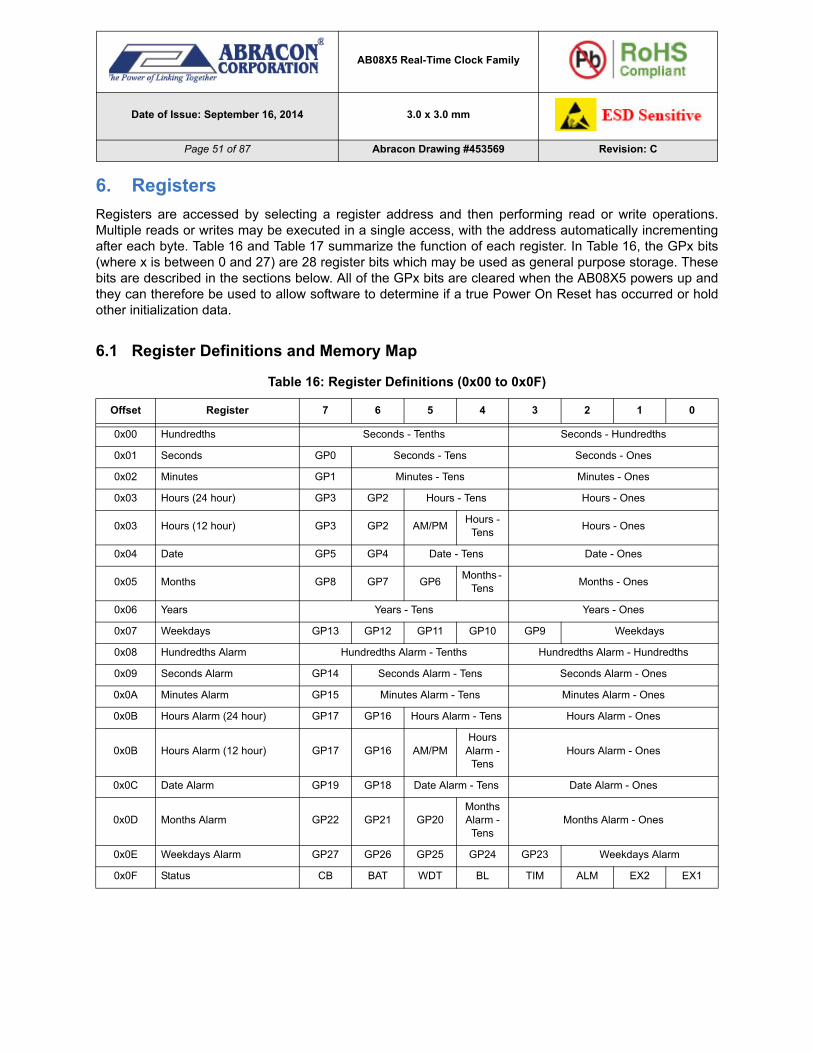
AB08X5 Real-Time Clock Family
Date of Issue: September 16, 2014 3.0 x 3.0 mm
Page 51 of 87 Abracon Drawing #453569 Revision: C
6. Registers
Registers are accessed by selecting a register address and then performing read or write operations.Multiple reads or writes may be executed in a single access, with the address automatically incrementingafter each byte. Table 16 and Table 17 summarize the function of each register. In Table 16, the GPx bits(where x is between 0 and 27) are 28 register bits which may be used as general purpose storage. Thesebits are described in the sections below. All of the GPx bits are cleared when the AB08X5 powers up andthey can therefore be used to allow software to determine if a true Power On Reset has occurred or holdother initialization data.
6.1 Register Definitions and Memory Map
Table 16: Register Definitions (0x00 to 0x0F)
Offset Register 7 6 5 4 3 2 1 0
0x00 Hundredths Seconds - Tenths Seconds - Hundredths
0x01 Seconds GP0 Seconds - Tens Seconds - Ones
0x02 Minutes GP1 Minutes - Tens Minutes - Ones
0x03 Hours (24 hour) GP3 GP2 Hours - Tens Hours - Ones
0x03 Hours (12 hour) GP3 GP2 AM/PMHours -
TensHours - Ones
0x04 Date GP5 GP4 Date - Tens Date - Ones
0x05 Months GP8 GP7 GP6Months -
TensMonths - Ones
0x06 Years Years - Tens Years - Ones
0x07 Weekdays GP13 GP12 GP11 GP10 GP9 Weekdays
0x08 Hundredths Alarm Hundredths Alarm - Tenths Hundredths Alarm - Hundredths
0x09 Seconds Alarm GP14 Seconds Alarm - Tens Seconds Alarm - Ones
0x0A Minutes Alarm GP15 Minutes Alarm - Tens Minutes Alarm - Ones
0x0B Hours Alarm (24 hour) GP17 GP16 Hours Alarm - Tens Hours Alarm - Ones
0x0B Hours Alarm (12 hour) GP17 GP16 AM/PMHours
Alarm - Tens
Hours Alarm - Ones
0x0C Date Alarm GP19 GP18 Date Alarm - Tens Date Alarm - Ones
0x0D Months Alarm GP22 GP21 GP20Months Alarm - Tens
Months Alarm - Ones
0x0E Weekdays Alarm GP27 GP26 GP25 GP24 GP23 Weekdays Alarm
0x0F Status CB BAT WDT BL TIM ALM EX2 EX1

AB08X5 Real-Time Clock Family
Date of Issue: September 16, 2014 3.0 x 3.0 mm
Page 52 of 87 Abracon Drawing #453569 Revision: C
Table 17: Register Definitions (0x10 to 0xFF)
Offset Register 7 6 5 4 3 2 1 0
0x10 Control1 STOP 12/24 OUTB OUT - ARST - WRTC
0x11 Control2 - - - OUT2S OUT1S
0x12 IntMask CEB IM BLIE TIE AIE EX2E EX1E
0x13 SQW SQWE - SQFS
0x14 Cal_XT CMDX OFFSETX
0x15 Cal_RC_Hi CMDR OFFSETR[13:8]
0x16 Cal_RC_Low OFFSETR[7:0]
0x17 Int Polarity - - EX2P EX1P - - - -
0x18 Timer Control TE TM TRPT RPT TFS
0x19 Timer Countdown Timer
0x1A Timer_Initial Timer Initial Value
0x1B WDT WDS BMB WRB
0x1C Osc. Control OSEL ACAL AOS FOS - OFIE ACIE
0x1D Osc. Status XTCAL LKO2 OMODE - - OF ACF
0x1E RESERVED RESERVED
0x1F Configuration Key Configuration Key
0x20 Trickle TCS DIODE ROUT
0x21 BREF Control BREF -
0x22 RESERVED RESERVED
0x23 RESERVED RESERVED
0x24 RESERVED RESERVED
0x25 RESERVED RESERVED
0x26 AFCTRL AFCTRL
0x27 BATMODE I/O IOBM RESERVED
0x28 ID0 (Read only) Part Number –MS Byte = 00001000 (0x08)
0x29 ID1 (Read only) Part Number – LS Byte (e.g. 00000101 for AB0805)
0x2A ID2 (Read only) Revision – Major = 00010 Revision – Minor = 011
0x2B ID3 (Read only) Lot[7:0]
0x2C ID4 (Read only) Lot[9] Unique ID[14:8]
0x2D ID5 (Read only) Unique ID[7:0]
0x2E ID6 (Read only) Lot[8] Wafer – –
0x2F ASTAT BBOD BMIN - - - - VINIT -
0x30 OCTRL WDBM EXBM - - - - - -
0x3F Extension Address - BPOL WDIN EXIN - XADA XADS
0x40–7F RAM Normal RAM Data
0x80–FF RAM Alternate RAM Data (I2C Mode Only)

AB08X5 Real-Time Clock Family
Date of Issue: September 16, 2014 3.0 x 3.0 mm
Page 53 of 87 Abracon Drawing #453569 Revision: C
6.2 Time and Date Registers
6.2.1 0x00 - Hundredths
This register holds the count of hundredths of seconds, in two binary coded decimal (BCD) digits. Valueswill be from 00 to 99. Note that in order to divide from 32.786 kHz, the hundredths register will not be fullyaccurate at all times but will be correct every 500 ms. Maximum jitter of this register will be less than 1 ms.The Hundredths Counter is not valid if the 128 Hz RC Oscillator is selected.
6.2.2 0x01 - Seconds
This register holds the count of seconds, in two binary coded decimal (BCD) digits. Values will be from 00to 59.
Table 18: Hundredths Register
Bit 7 6 5 4 3 2 1 0
Name Seconds - Tenths Seconds - Hundredths
Reset 1 0 0 1 1 0 0 1
Table 19: Hundredths Register Bits
Bit Name Function
7:4Seconds -
TenthsHolds the tenths place in the hundredths counter.
3:0Seconds -
HundredthsHolds the hundredths place in the hundredths counter.
Table 20: Seconds Register
Bit 7 6 5 4 3 2 1 0
Name GP0 Seconds - Tens Seconds - Ones
Reset 0 0 0 0 0 0 0 0
Table 21: Seconds Register Bits
Bit Name Function
7 GP0 Register bit for general purpose use.
6:4 Seconds - Tens Holds the tens place in the seconds counter.
3:0Seconds -
OnesHolds the ones place in the seconds counter.

AB08X5 Real-Time Clock Family
Date of Issue: September 16, 2014 3.0 x 3.0 mm
Page 54 of 87 Abracon Drawing #453569 Revision: C
6.2.3 0x02 - Minutes
This register holds the count of minutes, in two binary coded decimal (BCD) digits. Values will be from 00to 59.
6.2.4 0x03 - Hours
This register holds the count of hours, in two binary coded decimal (BCD) digits. Values will be from 00 to23 if the 12/24 bit (see 0x10 - Control1) is clear. If the 12/24 bit is set, the AM/PM bit will be 0 for AM hoursand 1 for PM hours, and hour values will range from 1 to 12.
Table 22: Minutes Register
Bit 7 6 5 4 3 2 1 0
Name GP1 Minutes - Tens Minutes - Ones
Reset 0 0 0 0 0 0 0 0
Table 23: Minutes Register Bits
Bit Name Function
7 GP1 Register bit for general purpose use.
6:4 Minutes - Tens Holds the tens place in the minutes counter.
3:0 Minutes - Ones Holds the ones place in the minutes counter.
Table 24: Hours Register (12 Hour Mode)
Bit 7 6 5 4 3 2 1 0
Name GP3 GP2 AM/PMHours -
TensHours - Ones
Reset 0 0 0 0 0 0 0 0
Table 25: Hours Register Bits (12 Hour Mode)
Bit Name Function
7 GP3 Register bit for general purpose use.
6 GP2 Register bit for general purpose use.
5 AM/PM 0 = AM hours. 1 = PM hours.
4 Hours - Tens Holds the tens place in the hours counter.
3:0 Hours - Ones Holds the ones place in the hours counter.

AB08X5 Real-Time Clock Family
Date of Issue: September 16, 2014 3.0 x 3.0 mm
Page 55 of 87 Abracon Drawing #453569 Revision: C
6.2.5 0x04 - Date
This register holds the current day of the month, in two binary coded decimal (BCD) digits. Values willrange from 01 to 31. Leap years are correctly handled from 1900 to 2199.
Table 26: Hours Register (24 Hour Mode)
Bit 7 6 5 4 3 2 1 0
Name GP3 GP2 Hours - Tens Hours - Ones
Reset 0 0 0 0 0 0 0 0
Table 27: Hours Register Bits (24 Hour Mode)
Bit Name Function
7 GP3 Register bit for general purpose use.
6 GP2 Register bit for general purpose use.
5:4 Hours - Tens Holds the tens place in the hours counter.
3:0 Hours - Ones Holds the ones place in the hours counter.
Table 28: Date Register
Bit 7 6 5 4 3 2 1 0
Name GP5 GP4 Date - Tens Date - Ones
Reset 0 0 0 0 0 0 0 1
Table 29: Date Register Bits
Bit Name Function
7 GP5 Register bit for general purpose use.
6 GP4 Register bit for general purpose use.
5:4 Date - Tens Holds the tens place in the date counter.
3:0 Date - Ones Holds the ones place in the date counter.

AB08X5 Real-Time Clock Family
Date of Issue: September 16, 2014 3.0 x 3.0 mm
Page 56 of 87 Abracon Drawing #453569 Revision: C
6.2.6 0x05 - Months
This register holds the current month, in two binary coded decimal (BCD) digits. Values will range from 01to 12.
6.2.7 0x06 - Years
This register holds the current year, in two binary coded decimal (BCD) digits. Values will range from 00 to99.
Table 30: Months Register
Bit 7 6 5 4 3 2 1 0
Name GP8 GP7 GP6Months -
TensMonths - Ones
Reset 0 0 0 0 0 0 0 1
Table 31: Months Register Bits
Bit Name Function
7 GP8 Register bit for general purpose use.
6 GP7 Register bit for general purpose use.
5 GP6 Register bit for general purpose use.
4 Months - Tens Holds the tens place in the months counter.
3:0 Months - Ones Holds the ones place in the months counter.
Table 32: Years Register
Bit 7 6 5 4 3 2 1 0
Name Years - Tens Years - Ones
Reset 0 0 0 0 0 0 0 0
Table 33: Years Register Bits
Bit Name Function
7:4 Years - Tens Holds the tens place in the years counter.
3:0 Years - Ones Holds the ones place in the years counter.

AB08X5 Real-Time Clock Family
Date of Issue: September 16, 2014 3.0 x 3.0 mm
Page 57 of 87 Abracon Drawing #453569 Revision: C
6.2.8 0x07 - Weekday
This register holds the current day of the week. Values will range from 0 to 6.
6.3 Alarm Registers
6.3.1 0x08 - Hundredths Alarm
This register holds the alarm value for hundredths of seconds, in two binary coded decimal (BCD) digits.Values will range from 00 to 99.
Table 34: Weekdays Register
Bit 7 6 5 4 3 2 1 0
Name GP13 GP12 GP11 GP10 GP9 Weekdays
Reset 0 0 0 0 0 0 0 0
Table 35: Weekdays Register Bits
Bit Name Function
7 GP13 Register bit for general purpose use.
6 GP12 Register bit for general purpose use.
5 GP11 Register bit for general purpose use.
4 GP10 Register bit for general purpose use.
3 GP9 Register bit for general purpose use.
2:0 Weekdays Holds the weekday counter value.
Table 36: Hundredths Alarm Register
Bit 7 6 5 4 3 2 1 0
Name Seconds Alarm - Tenths Seconds Alarm - Hundredths
Reset 0 0 0 0 0 0 0 0
Table 37: Hundredths Alarm Register Bits
Bit Name Function
7:4Seconds Alarm
- TenthsHolds the tenths place for the hundredths alarm.
3:0Seconds Alarm - Hundredths
Holds the hundredths place for the hundredths alarm.
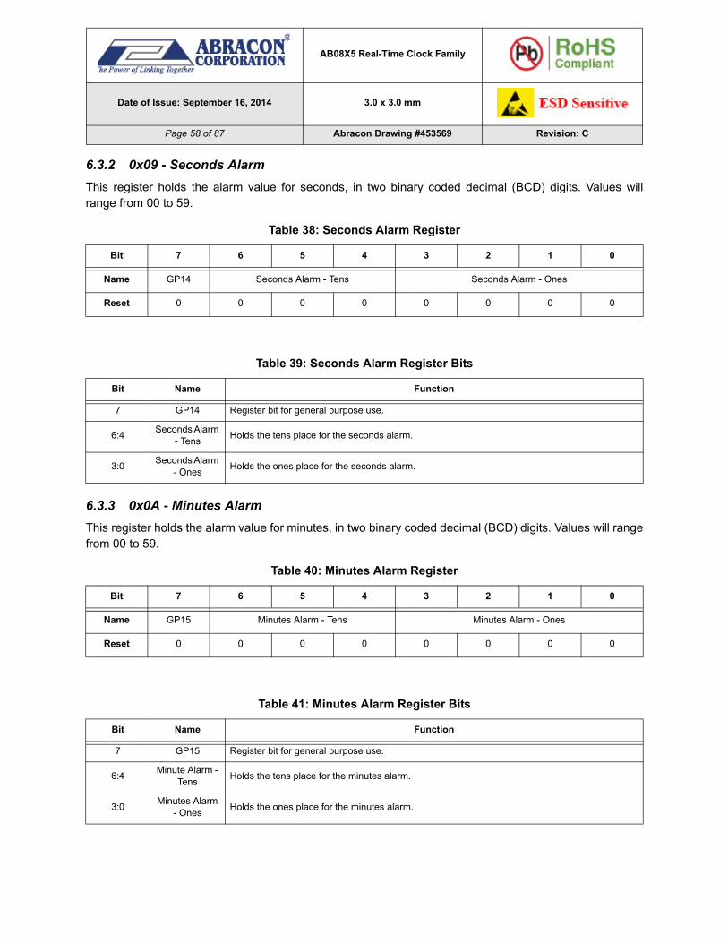
AB08X5 Real-Time Clock Family
Date of Issue: September 16, 2014 3.0 x 3.0 mm
Page 58 of 87 Abracon Drawing #453569 Revision: C
6.3.2 0x09 - Seconds Alarm
This register holds the alarm value for seconds, in two binary coded decimal (BCD) digits. Values willrange from 00 to 59.
6.3.3 0x0A - Minutes Alarm
This register holds the alarm value for minutes, in two binary coded decimal (BCD) digits. Values will rangefrom 00 to 59.
Table 38: Seconds Alarm Register
Bit 7 6 5 4 3 2 1 0
Name GP14 Seconds Alarm - Tens Seconds Alarm - Ones
Reset 0 0 0 0 0 0 0 0
Table 39: Seconds Alarm Register Bits
Bit Name Function
7 GP14 Register bit for general purpose use.
6:4Seconds Alarm
- TensHolds the tens place for the seconds alarm.
3:0Seconds Alarm
- OnesHolds the ones place for the seconds alarm.
Table 40: Minutes Alarm Register
Bit 7 6 5 4 3 2 1 0
Name GP15 Minutes Alarm - Tens Minutes Alarm - Ones
Reset 0 0 0 0 0 0 0 0
Table 41: Minutes Alarm Register Bits
Bit Name Function
7 GP15 Register bit for general purpose use.
6:4Minute Alarm -
TensHolds the tens place for the minutes alarm.
3:0Minutes Alarm
- OnesHolds the ones place for the minutes alarm.

AB08X5 Real-Time Clock Family
Date of Issue: September 16, 2014 3.0 x 3.0 mm
Page 59 of 87 Abracon Drawing #453569 Revision: C
6.3.4 0x0B - Hours Alarm
This register holds the alarm value for hours, in two binary coded decimal (BCD) digits. Values will rangefrom 00 to 23 if the 12/24 bit (see 0x10 - Control1) is clear. If the 12/24 bit is set, the AM/PM bit will be 0 forAM hours and 1 for PM hours, and hour values will be from 1 to 12.
Table 42: Hours Alarm Register (12 Hour Mode)
Bit 7 6 5 4 3 2 1 0
Name GP17 GP16 AM/PMHours
Alarm - Tens
Hours Alarm - Ones
Reset 0 0 0 0 0 0 0 0
Table 43: Hours Alarm Register Bits (12 Hour Mode)
Bit Name Function
7 GP17 Register bit for general purpose use.
6 GP16 Register bit for general purpose use.
5 AM/PM 0 = AM hours. 1 = PM hours.
4Hours Alarm -
TensHolds the tens place for the hours alarm.
3:0Hour Alarm -
OnesHolds the ones place for the hours alarm.
Table 44: Hours Alarm Register (24 Hour Mode)
Bit 7 6 5 4 3 2 1 0
Name GP17 GP16 Hours Alarm - Tens Hours Alarm - Ones
Reset 0 0 0 0 0 0 0 0
Table 45: Hours Alarm Register Bits (24 Hour Mode)
Bit Name Function
7 GP17 Register bit for general purpose use.
6 GP16 Register bit for general purpose use.
5:4Hours Alarm -
TensHolds the tens place for the hours alarm.
3:0Hours Alarm -
OnesHolds the ones place for the hours alarm.

AB08X5 Real-Time Clock Family
Date of Issue: September 16, 2014 3.0 x 3.0 mm
Page 60 of 87 Abracon Drawing #453569 Revision: C
6.3.5 0x0C - Date Alarm
This register holds alarm value for the date, in two binary coded decimal (BCD) digits. Values will rangefrom 01 to 31. Leap years are correctly handled from 1900 to 2199.
6.3.6 0x0D - Months Alarm
This register holds alarm value for months, in two binary coded decimal (BCD) digits. Values will rangefrom 01 to 12.
Table 46: Date Alarm Register
Bit 7 6 5 4 3 2 1 0
Name GP19 GP18 Date Alarm - Tens Date Alarm - Ones
Reset 0 0 0 0 0 0 0 0
Table 47: Date Alarm Register Bits
Bit Name Function
7 GP19 Register bit for general purpose use.
6 GP18 Register bit for general purpose use.
5:4 Date Alarm - Tens Holds the tens place for the date alarm.
3:0Date Alarm -
OnesHolds the ones place for the date alarm.
Table 48: Months Alarm Register
Bit 7 6 5 4 3 2 1 0
Name GP22 GP21 GP20Months Alarm - Tens
Months Alarm - Ones
Reset 0 0 0 0 0 0 0 0
Table 49: Months Alarm Register Bits
Bit Name Function
7 GP22 Register bit for general purpose use.
6 GP21 Register bit for general purpose use.
5 GP20 Register bit for general purpose use.
4Months Alarm -
TensHolds the tens place for the months alarm.
3:0Months Alarm -
OnesHolds the ones place for the months alarm.

AB08X5 Real-Time Clock Family
Date of Issue: September 16, 2014 3.0 x 3.0 mm
Page 61 of 87 Abracon Drawing #453569 Revision: C
6.3.7 0x0E - Weekday Alarm
This register holds the alarm value for the day of the week. Values will range from 0 to 6.
6.4 Configuration Registers
6.4.1 0x0F - Status (Read Only)
This register holds a variety of status bits. The register may be written at any time to clear or set any statusflag. If the ARST bit is set, any read of the Status Register will clear all of the bits except the CB bit.
Table 50: Weekdays Alarm Register
Bit 7 6 5 4 3 2 1 0
Name GP27 GP26 GP25 GP24 GP23 Weekdays Alarm
Reset 0 0 0 0 0 0 0 0
Table 51: Weekdays Alarm Register Bits
Bit Name Function
7 GP27 Register bit for general purpose use.
6 GP26 Register bit for general purpose use.
5 GP25 Register bit for general purpose use.
4 GP24 Register bit for general purpose use.
3 GP23 Register bit for general purpose use.
2:0 Weekdays Alarm Holds the weekdays alarm value.
Table 52: Status Register
Bit 7 6 5 4 3 2 1 0
Name CB BAT WDT BL TIM ALM EX2 EX1
Reset 0 0 0 0 0 0 0 0
Table 53: Status Register Bits
Bit Name Function
7 CBCentury. This bit will be toggled when the Years register rolls over from 99 to 00 if the CEB bit is a 1.A 0 assumes the century is 19xx or 21xx, and a 1 assumes it is 20xx for leap year calculations.
6 BAT Set when the system switches to the VBAT Power state.
5 WDT Set when the Watchdog Timer is enabled and is triggered, and the WDS bit is 0.
4 BLSet if the battery voltage VBAT crosses the reference voltage selected by BREF in the directionselected by BPOL.
3 TIM Set when the Countdown Timer is enabled and reaches zero.

AB08X5 Real-Time Clock Family
Date of Issue: September 16, 2014 3.0 x 3.0 mm
Page 62 of 87 Abracon Drawing #453569 Revision: C
6.4.2 0x10 - Control1
This register holds some major control signals.
2 ALMSet when the Alarm function is enabled and all selected Alarm registers match their respectivecounters.
1 EX2Set when an external trigger is detected on the WDI pin. The EX2E bit must be set in order for thisinterrupt to occur, but subsequently clearing EX2E will not automatically clear this flag.
0 EX1Set when an external trigger is detected on the EXTI pin. The EX1E bit must be set in order for thisinterrupt to occur, but subsequently clearing EX1E will not automatically clear this flag.
Table 54: Control1 Register
Bit 7 6 5 4 3 2 1 0
Name STOP 12/24 OUTB OUT RESERVED ARST RESERVED WRTC
Reset 0 0 0 1 0 0 0 1
Table 55: Control1 Register Bits
Bit Name Function
7 STOP
When 1, stops the clocking system. The XT and RC Oscillators are not stopped. In XT Modethe 32.786 kHz clock output will continue to run. In RC Mode, the 128 Hz clock output will con-tinue to run. Other clock output selections will produce static outputs. This bit allows the clocksystem to be precisely started, by setting it to 1 and back to 0.
6 12/24When 0, the Hours register operates in 24 hour mode. When 1, the Hours register operates in12 hour mode.
5 OUTBA static value which may be driven on the nIRQ2 pin. The OUTB bit cannot be set to 1 if theLKO2 bit is 1.
4 OUTA static value which may be driven on the FOUT/nIRQ pin. This bit also defines the defaultvalue for the Square Wave output when SQWE is not asserted.
3 RESERVED RESERVED
2 ARSTAuto reset enable. When 1, a read of the Status register will cause any interrupt bits (TIM, BL,ALM, WDT, XT1, XT2) to be cleared. When 0, the bits must be explicitly cleared by writing theStatus register.
1 RESERVED RESERVED
0 WRTCWrite RTC. This bit must be set in order to write any of the Counter registers (Hundredths, Sec-onds, Minutes, Hours, Date, Months, Years or Weekdays).
Table 53: Status Register Bits
Bit Name Function

AB08X5 Real-Time Clock Family
Date of Issue: September 16, 2014 3.0 x 3.0 mm
Page 63 of 87 Abracon Drawing #453569 Revision: C
6.4.3 0x11 - Control2
This register holds additional control and configuration signals for the flexible output pins FOUT/nIRQ and
nIRQ2. Note that nIRQ2 and FOUT/nIRQ are open drain outputs.
Table 56: Control2 Register
Bit 7 6 5 4 3 2 1 0
Name RESERVED OUT2S OUT1S
Reset 0 0 0 0 0 0 0 0
Table 57: Control2 Register Bits
Bit Name Function
7:5 RESERVED RESERVED
4:2 OUT2S Controls the function of the nIRQ2 pin, as shown in Table 58.
1:0 OUT1S Controls the function of the FOUT/NIRQ pin, as shown in Table 59.
Table 58: nIRQ2 Pin Control
OUT2S Value nIRQ2 Pin Function
000 nIRQ if at least one interrupt is enabled, else OUTB
001 SQW if SQWE = 1, else OUTB
010 RESERVED
011 nAIRQ if AIE is set, else OUTB
100 TIRQ if TIE is set, else OUTB
101 nTIRQ if TIE is set, else OUTB
110 RESERVED
111 OUTB
Table 59: FOUT/nIRQ Pin Control
OUT1S Value FOUT/nIRQ Pin Function
00 nIRQ if at least one interrupt is enabled, else OUT
01 SQW if SQWE = 1, else OUT
10 SQW if SQWE = 1, else nIRQ if at least one interrupt is enabled, else OUT
11 nAIRQ if AIE is set, else OUT
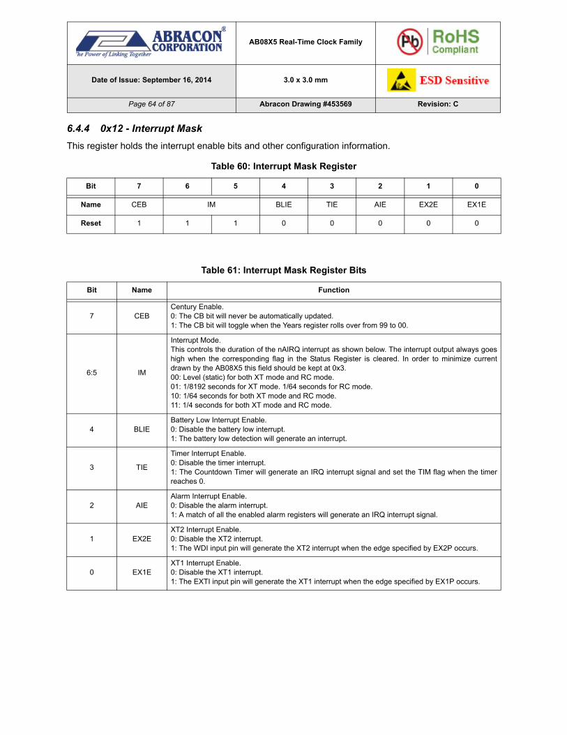
AB08X5 Real-Time Clock Family
Date of Issue: September 16, 2014 3.0 x 3.0 mm
Page 64 of 87 Abracon Drawing #453569 Revision: C
6.4.4 0x12 - Interrupt Mask
This register holds the interrupt enable bits and other configuration information.
Table 60: Interrupt Mask Register
Bit 7 6 5 4 3 2 1 0
Name CEB IM BLIE TIE AIE EX2E EX1E
Reset 1 1 1 0 0 0 0 0
Table 61: Interrupt Mask Register Bits
Bit Name Function
7 CEBCentury Enable. 0: The CB bit will never be automatically updated.1: The CB bit will toggle when the Years register rolls over from 99 to 00.
6:5 IM
Interrupt Mode.This controls the duration of the nAIRQ interrupt as shown below. The interrupt output always goeshigh when the corresponding flag in the Status Register is cleared. In order to minimize currentdrawn by the AB08X5 this field should be kept at 0x3.00: Level (static) for both XT mode and RC mode.01: 1/8192 seconds for XT mode. 1/64 seconds for RC mode.10: 1/64 seconds for both XT mode and RC mode.11: 1/4 seconds for both XT mode and RC mode.
4 BLIEBattery Low Interrupt Enable.0: Disable the battery low interrupt.1: The battery low detection will generate an interrupt.
3 TIE
Timer Interrupt Enable. 0: Disable the timer interrupt.1: The Countdown Timer will generate an IRQ interrupt signal and set the TIM flag when the timerreaches 0.
2 AIEAlarm Interrupt Enable.0: Disable the alarm interrupt.1: A match of all the enabled alarm registers will generate an IRQ interrupt signal.
1 EX2EXT2 Interrupt Enable.0: Disable the XT2 interrupt.1: The WDI input pin will generate the XT2 interrupt when the edge specified by EX2P occurs.
0 EX1EXT1 Interrupt Enable.0: Disable the XT1 interrupt.1: The EXTI input pin will generate the XT1 interrupt when the edge specified by EX1P occurs.

AB08X5 Real-Time Clock Family
Date of Issue: September 16, 2014 3.0 x 3.0 mm
Page 65 of 87 Abracon Drawing #453569 Revision: C
6.4.5 0x13 - SQW
This register holds the control signals for the square wave output. Note that some frequency selections arenot valid if the 128 Hz RC Oscillator is selected.
Table 62: SQW Register
Bit 7 6 5 4 3 2 1 0
Name SQWE RESERVED SQFS
Reset 0 0 1 0 0 1 1 0
Table 63: SQW Register Bits
Bit Name Function
7 SQWEWhen 1, the square wave output is enabled. When 0, the square wave output is held at thevalue of OUT.
6:5 RESERVED RESERVED
4:0 SQFSSelects the frequency of the square wave output, as shown in Table 64. Note that some selec-tions are not valid if the 128 Hz oscillator is selected. Some selections also produce shortpulses rather than square waves, and are intended primarily for test usage.
Table 64: Square Wave Function Select
SQFS Value Square Wave Output
00000 1 century(2)
00001 32.768 kHz(1)
00010 8.192 kHz(1)
00011 4.096 kHz(1)
00100 2.048 kHz(1)
00101 1.024 kHz(1)
00110 512 Hz(1) – Default value
00111 256 Hz(1)
01000 128 Hz
01001 64 Hz
01010 32 Hz
01011 16 Hz
01100 8 Hz
01101 4 Hz
01110 2 Hz
01111 1 Hz

AB08X5 Real-Time Clock Family
Date of Issue: September 16, 2014 3.0 x 3.0 mm
Page 66 of 87 Abracon Drawing #453569 Revision: C
6.5 Calibration Registers
6.5.1 0x14 - Calibration XT
This register holds the control signals for a digital calibration function of the XT Oscillator.
10000 ½ Hz
10001 ¼ Hz
10010 1/8 Hz
10011 1/16 Hz
10100 1/32 Hz
10101 1/60 Hz (1 minute)
10110 16.384 kHz (1)
10111 100 Hz (1)(2)
11000 1 hour(2)
11001 1 day(2)
11010 TIRQ
11011 NOT TIRQ
11100 1 year(2)
11101 1 Hz to Counters(2)
11110 1/32 Hz from Acal(2)
11111 1/8 Hz from Acal (2)
(1) NA if 128 Hz Oscillator selected.(2) Pulses for Test Usage.
Table 65: Calibration XT Register
Bit 7 6 5 4 3 2 1 0
Name CMDX OFFSETX
Reset 0 0 0 0 0 0 0 0
Table 66: Calibration XT Register Bits
Bit Name Function
7 CMDXThe calibration adjust mode. When 0 (Normal Mode), each adjustment step is +/- 2 ppm. When1 (Coarse Mode), each adjustment step is +/- 4 ppm.
6:0 OFFSETXThe amount to adjust the effective time. This is a two's complement number with a range of -64to +63 adjustment steps.
Table 64: Square Wave Function Select
SQFS Value Square Wave Output

AB08X5 Real-Time Clock Family
Date of Issue: September 16, 2014 3.0 x 3.0 mm
Page 67 of 87 Abracon Drawing #453569 Revision: C
6.5.2 0x15 - Calibration RC Upper
This register holds the control signals for the fine digital calibration function of the low power RC Oscillator.This register is initialized with a factory value which calibrates the RC Oscillator to 128 Hz.
6.5.3 0x16 - Calibration RC Lower
This register holds the lower 8 bits of the OFFSETR field for the digital calibration function of the low powerRC Oscillator. This register is initialized with a factory value which calibrates the RC Oscillator to 128 Hz.
Table 67: Calibration RC Upper Register
Bit 7 6 5 4 3 2 1 0
Name CMDR OFFSETRU
Reset Preconfigured Preconfigured
Table 68: Calibration RC Upper Register Bits
Bit Name Function
7:6 CMDRThe calibration adjust mode for the RC calibration adjustment. CMDR selects the highest fre-quency used in the RC Calibration process, as shown in Table 69.
5:0 OFFSETRUThe upper 6 bits of the OFFSETR field, which is used to set the amount to adjust the effectivetime. OFFSETR is a two's complement number with a range of -2^13 to +2^13-1 adjustmentsteps.
Table 69: CMDR Function
CMDR Calibration Period Minimum Adjustment Maximum Adjustment
00 8,192 seconds +/-1.91 ppm +/-1.56%
01 4,096 seconds +/-3.82 ppm +/-3.13%
10 2,048 seconds +/-7.64 ppm +/-6.25%
11 1,024 seconds +/-15.28 ppm +/-12.5%
Table 70: Calibration RC Lower Register
Bit 7 6 5 4 3 2 1 0
Name OFFSETRL
Reset Preconfigured
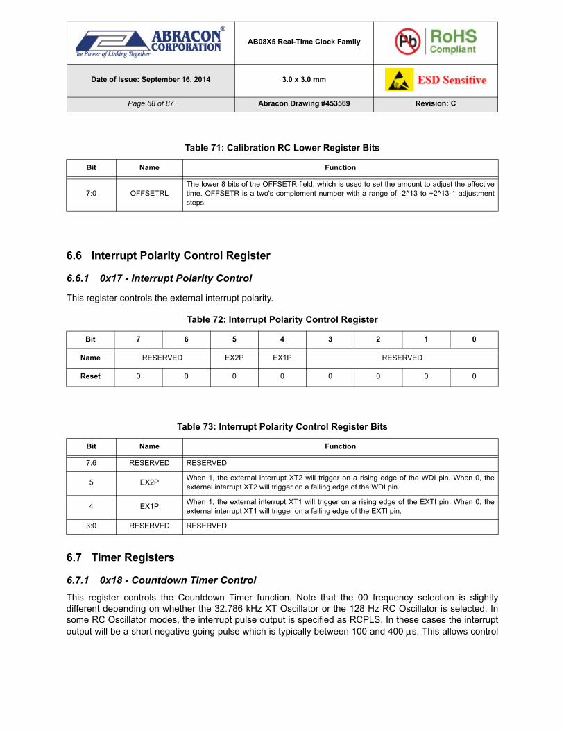
AB08X5 Real-Time Clock Family
Date of Issue: September 16, 2014 3.0 x 3.0 mm
Page 68 of 87 Abracon Drawing #453569 Revision: C
6.6 Interrupt Polarity Control Register
6.6.1 0x17 - Interrupt Polarity Control
This register controls the external interrupt polarity.
6.7 Timer Registers
6.7.1 0x18 - Countdown Timer Control
This register controls the Countdown Timer function. Note that the 00 frequency selection is slightlydifferent depending on whether the 32.786 kHz XT Oscillator or the 128 Hz RC Oscillator is selected. Insome RC Oscillator modes, the interrupt pulse output is specified as RCPLS. In these cases the interruptoutput will be a short negative going pulse which is typically between 100 and 400 s. This allows control
Table 71: Calibration RC Lower Register Bits
Bit Name Function
7:0 OFFSETRLThe lower 8 bits of the OFFSETR field, which is used to set the amount to adjust the effectivetime. OFFSETR is a two's complement number with a range of -2^13 to +2^13-1 adjustmentsteps.
Table 72: Interrupt Polarity Control Register
Bit 7 6 5 4 3 2 1 0
Name RESERVED EX2P EX1P RESERVED
Reset 0 0 0 0 0 0 0 0
Table 73: Interrupt Polarity Control Register Bits
Bit Name Function
7:6 RESERVED RESERVED
5 EX2PWhen 1, the external interrupt XT2 will trigger on a rising edge of the WDI pin. When 0, theexternal interrupt XT2 will trigger on a falling edge of the WDI pin.
4 EX1PWhen 1, the external interrupt XT1 will trigger on a rising edge of the EXTI pin. When 0, theexternal interrupt XT1 will trigger on a falling edge of the EXTI pin.
3:0 RESERVED RESERVED

AB08X5 Real-Time Clock Family
Date of Issue: September 16, 2014 3.0 x 3.0 mm
Page 69 of 87 Abracon Drawing #453569 Revision: C
of external devices which require pulses shorter than the minimum 7.8 ms pulse created directly by the RCOscillator.
Table 74: Countdown Timer Control Register
Bit 7 6 5 4 3 2 1 0
Name TE TM TRPT RPT TFS
Reset 0 0 1 0 0 0 1 1
Table 75: Countdown Timer Control Register Bits
Bit Name Function
7 TETimer Enable. When 1, the Countdown Timer will count down. When 0, the Countdown Timer retainsthe current value. If TE is 0, the clock to the Timer is disabled for power minimization.
6 TM
Timer Interrupt Mode. Along with TRPT, this controls the Timer Interrupt function as shown in Table28. A Level Interrupt will cause the nIRQ signal to be driven low by a Countdown Timer interrupt untilthe associated flag is cleared. A Pulse interrupt will cause the nIRQ signal to be driven low for thetime shown in Table 77 or until the flag is cleared.
5 TRPT
Along with TM, this controls the repeat function of the Countdown Timer. If Repeat is selected, theCountdown Timer reloads the value from the Timer_Initial register upon reaching 0, and continuescounting. If Single is selected, the Countdown Timer will halt when it reaches zero. This allows thegeneration of periodic interrupts of virtually any frequency.
4:2 RPTThese bits enable the Alarm Interrupt repeat function, as shown in Table 76. HA is the Hun-dredths_Alarm register value.
1:0 TFSSelect the clock frequency and interrupt pulse width of the Countdown Timer, as defined in Table 77.RCPLS is a 100-400 s pulse.
Table 76: Repeat Function
RPT HA Repeat When
7 FF Once per hundredth (*)
7 F[9-0] Once per tenth (*)
7 [9-0][9-0] Hundredths match (once per second)
6 Hundredths and seconds match (once per minute)
5 Hundredths, seconds and minutes match (once per hour)
4 Hundredths, seconds, minutes and hours match (once per day)
3 Hundredths, seconds, minutes, hours and weekday match (once per week)
2 Hundredths, seconds, minutes, hours and date match (once per month)
1 Hundredths, seconds, minutes, hours, date and month match (once per year)
0 Alarm Disabled
(*)Once per second if 128 Hz Oscillator selected

AB08X5 Real-Time Clock Family
Date of Issue: September 16, 2014 3.0 x 3.0 mm
Page 70 of 87 Abracon Drawing #453569 Revision: C
6.7.2 0x19 - Countdown Timer
This register holds the current value of the Countdown Timer. It may be loaded with the desired startingvalue when the Countdown Timer is stopped.
Table 77: Countdown Timer Function Select
TM TRPT TFS Int Repeat Countdown Timer Frequency Interrupt Pulse Width
32.786 kHz Oscil-lator
128 Hz Oscillator32.786 kHzOscillator
128 Hz Oscillator
0 0 00 Pulse Single 4.096 kHz 128 Hz 1/4096 s 1/128 s
0 0 01 Pulse Single 64 Hz 64 Hz 1/128 s 1/128 s
0 0 10 Pulse Single 1 Hz 1 Hz 1/64 s 1/64 s
0 0 11 Pulse Single 1/60 Hz 1/60 Hz 1/64 s 1/64 s
0 1 00 Pulse Repeat 4.096 kHz 128 Hz 1/4096 s 1/128 s
0 1 01 Pulse Repeat 64 Hz 64 Hz 1/128 s 1/128 s
0 1 10 Pulse Repeat 1 Hz 1 Hz 1/64 s 1/64 s
0 1 11 Pulse Repeat 1/60 Hz 1/60 Hz 1/64 s 1/64 s
1 0 00 Level Single 4.096 kHz 128 Hz N/A N/A
1 0 01 Level Single 64 Hz 64 Hz N/A N/A
1 0 10 Level Single 1 Hz 1 Hz N/A N/A
1 0 11 Level Single 1/60 Hz 1/60 Hz N/A N/A
1 1 00 Pulse Repeat 4.096 kHz 128 Hz 1/4096 s RCPLS
1 1 01 Pulse Repeat 64 Hz 64 Hz 1/4096 s RCPLS
1 1 10 Pulse Repeat 1 Hz 1 Hz 1/4096 s RCPLS
1 1 11 Pulse Repeat 1/60 Hz 1/60 Hz 1/4096 s RCPLS
Table 78: Countdown Timer Register
Bit 7 6 5 4 3 2 1 0
Name Countdown Timer
Reset 0 0 0 0 0 0 0 0
Table 79: Countdown Timer Register Bits
Bit Name Function
7:0Countdown
TimerThe current value of the Countdown Timer.

AB08X5 Real-Time Clock Family
Date of Issue: September 16, 2014 3.0 x 3.0 mm
Page 71 of 87 Abracon Drawing #453569 Revision: C
6.7.3 0x1A - Timer Initial Value
This register holds the value which will be reloaded into the Countdown Timer when it reaches zero if theTRPT bit is a 1. This allows for periodic timer interrupts, and a period of (Timer_initial + 1) * (1/Countdown_frequency).
6.7.4 0x1B - Watchdog Timer
This register controls the Watchdog Timer function.
Table 80: Timer Initial Value Register
Bit 7 6 5 4 3 2 1 0
Name Timer Initial Value
Reset 0 0 0 0 0 0 0 0
Table 81: Timer Initial Value Register Bits
Bit Name Function
7:0Timer Initial
ValueThe value reloaded into the Countdown Timer when it reaches zero if the TRPT bit is a 1.
Table 82: Watchdog Timer Register
Bit 7 6 5 4 3 2 1 0
Name WDS BMB WRB
Reset 0 0 0 0 0 0 0 0
Table 83: Watchdog Timer Register Bits
Bit Name Function
7 WDSWatchdog Steering. When 0, the Watchdog Timer will generate WIRQ when it times out. When 1,the Watchdog Timer will generate a reset when it times out.
6:2 BMBThe number of clock cycles which must occur before the Watchdog Timer times out. A value of00000 disables the Watchdog Timer function.
1:0 WRB The clock frequency of the Watchdog Timer, as shown in Table 84.

AB08X5 Real-Time Clock Family
Date of Issue: September 16, 2014 3.0 x 3.0 mm
Page 72 of 87 Abracon Drawing #453569 Revision: C
6.8 Oscillator Registers
6.8.1 0x1C - Oscillator Control
This register controls the overall Oscillator function. It may only be written if the Configuration Key registercontains the value 0xA1. An Autocalibration cycle is initiated immediately whenever this register is writtenwith a value in the ACAL field which is not zero.
Table 84: Watchdog Timer Frequency Select
WRB Value Watchdog Timer Frequency
00 16 Hz
01 4 Hz
10 1 Hz
11 1/4 Hz
Table 85: Oscillator Control Register
Bit 7 6 5 4 3 2 1 0
Name OSEL ACAL AOS FOS RESERVED OFIE ACIE
Reset 0 0 0 0 0 0 0 0
Table 86: Oscillator Control Register Bits
Bit Name Function
7 OSEL
When 1, request the RC Oscillator to generate a 128 Hz clock for the timer circuits. When 0,request the XT Oscillator to generate a 32.786 kHz clock to the timer circuit. Note that if the XTOscillator is not operating, the oscillator switch will not occur. The OMODE field in the OscillatorStatus register indicates the actual oscillator which is selected.
6:5 ACAL Controls the automatic calibration function, as described in Autocalibration.
4 AOSWhen 1, the oscillator will automatically switch to RC oscillator mode when the system is poweredfrom the battery. When 0, no automatic switching occurs.
3 FOSWhen 1, the oscillator will automatically switch to RC oscillator mode when an oscillator failure isdetected. When 0, no automatic switching occurs.
2 RESERVED RESERVED
1 OFIE Oscillator Fail interrupt enable. When 1, an Oscillator Failure will generate an IRQ signal.
0 ACIE When 1, an Autocalibration Failure will generate an interrupt.

AB08X5 Real-Time Clock Family
Date of Issue: September 16, 2014 3.0 x 3.0 mm
Page 73 of 87 Abracon Drawing #453569 Revision: C
6.8.2 0x1D – Oscillator Status Register
This register holds several miscellaneous bits used to control and observe the oscillators.
6.9 Miscellaneous Registers
6.9.1 0x1F - Configuration Key
This register contains the Configuration Key, which must be written with specific values in order to accesssome registers and functions. The Configuration Key is reset to 0x00 on any register write.
Table 87: Oscillator Status Register
Bit 7 6 5 4 3 2 1 0
Name XTCAL LKO2 OMODE RESERVED OF ACF
Reset 0 0 1 0 0 0 1 0
Table 88: Oscillator Status Register Bits
Bit Name Function
7:6 XTCAL
Extended Crystal Calibration. This field defines a value by which the Crystal Oscillator is adjustedto compensate for low capacitance crystals, independent of the normal Crystal Calibration func-tion controlled by the Calibration XT Register. The frequency generated by the Crystal Oscillatoris slowed by 122 ppm times the value in the XTCAL field (0, -122,-244 or -366 ppm).
5 LKO2Lock OUT2. If this bit is a 1, the OUTB register bit (see Section 7.3.2) cannot be set to 1. This istypically used when OUT2 is configured as a power switch, and setting OUTB to a 1 would turn offthe switch.
4 OMODE(read only) – Oscillator Mode. This bit is a 1 if the RC Oscillator is selected to drive the internalclocks, and a 0 if the Crystal Oscillator is selected. If the STOP bit is set, the OMODE bit is invalid.
3:2 RESERVED RESERVED
1 OFOscillator Failure. This bit is set on a power on reset, when both the system and battery voltageshave dropped below acceptable levels. It is also set if an Oscillator Failure occurs, indicating thatthe crystal oscillator is running at less than 8 kHz. It can be cleared by writing a 0 to the bit.
0 ACFSet when an Autocalibration Failure occurs, indicating that either the RC Oscillator frequency istoo different from 128 Hz to be correctly calibrated or the XT Oscillator did not start.
Table 89: Configuration Key Register
Bit 7 6 5 4 3 2 1 0
Name Configuration Key
Reset 0 0 0 0 0 0 0 0

AB08X5 Real-Time Clock Family
Date of Issue: September 16, 2014 3.0 x 3.0 mm
Page 74 of 87 Abracon Drawing #453569 Revision: C
1. Writing a value of 0xA1 enables write access to the Oscillator Control register
2. Writing a value of 0x3C does not update the Configuration Key register, but generates a SoftwareReset (see Software Reset).
3. Writing a value of 0x9D enables write access to the Trickle Register (0x20), the BREF Register(0x21), the AFCTRL Register (0x26), the Batmode I/O Register (0x27) and the Output Control Regis-ter (0x30).
6.10 Analog Control Registers
6.10.1 0x20 - Trickle
This register controls the Trickle Charger. The Key Register must be written with the value 0x9D in order toenable access to this register.
Table 90: Configuration Key Register Bits
Bit Name Function
7:0Configuration
KeyWritten with specific values in order to access some registers and functions.
Table 91: Trickle Register
Bit 7 6 5 4 3 2 1 0
Name TCS DIODE ROUT
Reset 0 0 0 0 0 0 0 0
Table 92: Trickle Register Bits
Bit Name Function
7:4 TCS A value of 1010 enables the trickle charge function. All other values disable the Trickle Charger.
3:2 DIODEDiode Select. A value of 10 inserts a standard diode into the trickle charge circuit, with a voltagedrop of 0.6V. A value of 01 inserts a schottky diode into the trickle charge circuit, with a voltage dropof 0.3V. Other values disable the Trickle Charger.
1:0 ROUT Output Resistor. This selects the output resistor of the trickle charge circuit, as shown in Table 93.
Table 93: Trickle Charge Output Resistor
ROUT Value Series Resistor
00 Disable
01 3 KΩ
10 6 KΩ
11 11 KΩ

AB08X5 Real-Time Clock Family
Date of Issue: September 16, 2014 3.0 x 3.0 mm
Page 75 of 87 Abracon Drawing #453569 Revision: C
6.10.2 0x21 - BREF Control
This register controls the reference voltages used in the Wakeup Control system. The Key Register must
be written with the value 0x9D in order to enable access to this register.
6.10.3 0x26 – AFCTRL
This register holds the enable code for the Autocalibration Filter (AF) filter capacitor connected to the AFpin. Writing the value 0xA0 to this register enables the AF pin. Writing the value 0x00 to this registerdisables the AF pin. No other value may be written to this register. The Configuration Key Register must bewritten with the value 0x9D prior to writing the AFCTRL Register.
Table 94: BREF Control Register
Bit 7 6 5 4 3 2 1 0
Name BREF RESERVED
Reset 1 1 1 1 0 0 0 0
Table 95: BREF Control Register Bits
Bit Name Function
7:4 BREFThis selects the voltage reference which is compared to the battery voltage VBAT to produce theBBOD signal. Typical values are shown in Table 96. The valid BREF values are 0x7, 0xB, 0xD,and 0xF. The reset value is 0xF. All other values are RESERVED.
3:0 RESERVED RESERVED
Table 96: VBAT Reference Voltage
BREF Value VBAT Falling Voltage (TYP) VBAT Rising Voltage (TYP)
0111 2.5V 3.0V
1011 2.1V 2.5V
1101 1.8V 2.2V
1111 1.4V 1.6V
Table 97: AFCTRL Register
Bit 7 6 5 4 3 2 1 0
Name AFCTRL
Reset 0 0 0 0 0 0 0 0

AB08X5 Real-Time Clock Family
Date of Issue: September 16, 2014 3.0 x 3.0 mm
Page 76 of 87 Abracon Drawing #453569 Revision: C
6.10.4 0x27 – Batmode IO Register
This register holds the IOBM bit which controls the enabling and disabling of the I/O interface when aBrownout Detection occurs. It may only be written if the Configuration Key register contains the value0x9D. All undefined bits must be written with 0.
6.10.5 0x2F – Analog Status Register (Read Only)
This register holds eight status bits which indicate the voltage levels of the VCC and VBAT power inputs.
Table 98: AFCTRL Register Bits
Bit Name Function
7:0 AFCTRL If 0xA0, enable the AF pin. If 0x00, disable the AF pin.
Table 99: Batmode IO Register
Bit 7 6 5 4 3 2 1 0
Name IOBM RESERVED
Reset 1 0 0 0 0 0 0 0
Table 100: Batmode IO Register Bits
Bit Name Function
7 IOBMIf 1, the AB08X5 will not disable the I/O interface even if VCC goes away and VBAT is still present.This allows external access while the AB08X5 is powered by VBAT.
6:0 RESERVED RESERVED - must write only 0000000.
Table 101: Analog Status Register
Bit 7 6 5 4 3 2 1 0
Name BBOD BMIN RESERVED VINIT RESERVED
Reset

AB08X5 Real-Time Clock Family
Date of Issue: September 16, 2014 3.0 x 3.0 mm
Page 77 of 87 Abracon Drawing #453569 Revision: C
6.10.6 0x30 – Output Control Register
This register holds bits which control the behavior of the I/O pins under various power down conditions.
The Key Register must be written with the value 0x9D in order to enable access to this register.
6.11 ID Registers
6.11.1 0x28 – ID0 - Part Number Upper Register (Read Only)
This register holds the upper eight bits of the part number in BCD format, which is always 0x08 for theAB08X5 family.
Table 102: Analog Status Register Bits
Bit Name Function
7 BBOD If 1, the VBAT input voltage is above the BREF threshold.
6 BMIN If 1, the VBAT input voltage is above the minimum operating voltage (1.2 V).
5:2 RESERVED RESERVED
1 VINIT If 1, the VCC input voltage is above the minimum power up voltage (1.6 V).
0 RESERVED RESERVED
Table 103: Output Control Register
Bit 7 6 5 4 3 2 1 0
Name WDBM EXBM RESERVED
Reset 0 0 0 0 0 0 0 0
Table 104: Output Control Register Bits
Bit Name Function
7 WDBMIf 1, the WDI input is enabled when the AB08X5 is powered from VBAT. If 0, the WDI input is dis-abled when the AB08X5 is powered from VBAT.
6 EXBMIf 1, the EXTI input is enabled when the AB08X5 is powered from VBAT. If 0, the EXTI input is dis-abled when the AB08X5 is powered from VBAT.
5:0 RESERVED
Table 105: 28 – ID0 – Part Number Upper Register
Bit 7 6 5 4 3 2 1 0
Name Part Number - Digit 3 Part Number - Digit 2
Reset 0 0 0 0 1 0 0 0

AB08X5 Real-Time Clock Family
Date of Issue: September 16, 2014 3.0 x 3.0 mm
Page 78 of 87 Abracon Drawing #453569 Revision: C
6.11.2 0x29 – ID1 - Part Number Lower Register (Read Only)
This register holds the lower eight bits of the part number in BCD format.
6.11.3 0x2A – ID2 - Part Revision (Read Only)
This register holds the Revision number of the part.
6.11.4 0x2B – ID3 – Lot Lower (Read Only)
This register holds the lower 8 bits of the manufacturing lot number.
Table 106: 28 – ID1 – Part Number Lower Register
Bit 7 6 5 4 3 2 1 0
Name Part Number - Digit 1 Part Number - Digit 0
Reset Preconfigured Digit 1 Preconfigured Digit 0
Table 107: 2A – ID2 – Part Revision Register
Bit 7 6 5 4 3 2 1 0
Name MAJOR MINOR
Reset 0 0 0 1 0 0 1 1
Table 108: 2A – ID2 – Part Revision Register Bits
Bit Name Function
7:3 MAJOR This field holds the major revision of the AB08X5.
2:0 MINOR This field holds the minor revision of the AB08X5.
Table 109: 2B – ID3 – Lot Lower Register
Bit 7 6 5 4 3 2 1 0
Name Lot[7:0]
Reset Preconfigured Lot Number
Table 110: 2B – ID3 – Lot Lower Register Bits
Bit Name Function
7:0 Lot[7:0] This field holds the lower 8 bits of the manufacturing lot number.

AB08X5 Real-Time Clock Family
Date of Issue: September 16, 2014 3.0 x 3.0 mm
Page 79 of 87 Abracon Drawing #453569 Revision: C
6.11.5 0x2C – ID4 – ID Upper (Read Only)
This register holds part of the manufacturing information of the part, including bit 9 of the manufacturing lotnumber and the upper 7 bits of the unique part identifier. The 15-bit ID field contains a unique value for
each AB08X5 part.
6.11.6 0x2D – ID5 – Unique Lower (Read Only)
This register holds the lower 8 bits of the unique part identifier. The 15-bit ID field contains a unique value
for each AB08X5 part.
Table 111: 2C – ID4 – ID Upper Register
Bit 7 6 5 4 3 2 1 0
Name Lot[9] ID[14:8]
Reset Preconfigured Value
Table 112: 2C – ID4 – ID Upper Register Bits
Bit Name Function
7 Lot[9] This field holds bit 9 of the manufacturing lot number.
1:0 ID[14:8] This field holds the upper 7 bits of the unique part ID.
Table 113: 2D – ID5 – ID Lower Register
Bit 7 6 5 4 3 2 1 0
Name ID]7:0]
Reset Preconfigured Value
Table 114: 2D – ID5 – ID Lower Register Bits
Bit Name Function
7:0 ID[7:0] This field holds the lower 8 bits of the unique part ID.
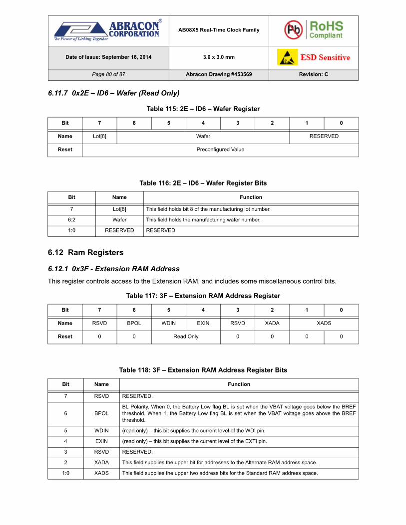
AB08X5 Real-Time Clock Family
Date of Issue: September 16, 2014 3.0 x 3.0 mm
Page 80 of 87 Abracon Drawing #453569 Revision: C
6.11.7 0x2E – ID6 – Wafer (Read Only)
6.12 Ram Registers
6.12.1 0x3F - Extension RAM Address
This register controls access to the Extension RAM, and includes some miscellaneous control bits.
Table 115: 2E – ID6 – Wafer Register
Bit 7 6 5 4 3 2 1 0
Name Lot[8] Wafer RESERVED
Reset Preconfigured Value
Table 116: 2E – ID6 – Wafer Register Bits
Bit Name Function
7 Lot[8] This field holds bit 8 of the manufacturing lot number.
6:2 Wafer This field holds the manufacturing wafer number.
1:0 RESERVED RESERVED
Table 117: 3F – Extension RAM Address Register
Bit 7 6 5 4 3 2 1 0
Name RSVD BPOL WDIN EXIN RSVD XADA XADS
Reset 0 0 Read Only 0 0 0 0
Table 118: 3F – Extension RAM Address Register Bits
Bit Name Function
7 RSVD RESERVED.
6 BPOLBL Polarity. When 0, the Battery Low flag BL is set when the VBAT voltage goes below the BREFthreshold. When 1, the Battery Low flag BL is set when the VBAT voltage goes above the BREFthreshold.
5 WDIN (read only) – this bit supplies the current level of the WDI pin.
4 EXIN (read only) – this bit supplies the current level of the EXTI pin.
3 RSVD RESERVED.
2 XADA This field supplies the upper bit for addresses to the Alternate RAM address space.
1:0 XADS This field supplies the upper two address bits for the Standard RAM address space.
AB08X5 Real-Time Clock Family
Date of Issue: September 16, 2014 3.0 x 3.0 mm
Page 81 of 87 Abracon Drawing #453569 Revision: C
6.12.2 0x40 - 0x7F – Standard RAM
64 bytes of RAM space which may be accessed in either I2C or SPI interface mode. The data in the RAMis held when using battery power. The upper 2 bits of the RAM address are taken from the XADS field, andthe lower 6 bits are taken from the address offset, supporting a total RAM of 256 bytes. The initial values ofthe RAM locations are undefined.
6.12.3 0x80 - 0xFF – Alternate RAM
128 bytes of RAM which may be accessed only in I2C interface mode. The data in the RAM is held whenusing battery power. The upper bit of the RAM address is taken from the XADA field, and the lower 7 bitsare taken from the address offset, supporting a total RAM of 256 bytes. The initial values of the RAMlocations are undefined.

AB08X5 Real-Time Clock Family
Date of Issue: September 16, 2014 3.0 x 3.0 mm
Page 82 of 87 Abracon Drawing #453569 Revision: C
7. Package Mechanical Information
Figure 32 illustrates the package mechanical information.
Figure 32. Package Mechanical Diagram
3.00 ± 0.05
3.00±0.05
0.85± 0.05
0.00 –0.05 Seating
Plane
0.20 REF
0.35 ± 0.05
0.25 ±0.05
x16
1.80±0.10
1.80 ± 0.10
0.25 REF
PACKAGE TOP VIEW
PACKAGE SIDE VIEW
PACKAGE BOTTOM VIEW
Thermal Pad0.25REF
1
Drawing Notes:1. All dimensions are in millimeters.2. These drawings are subject to change without notice.3. Quad Flat‐pack, No‐leads (QFN) package configuration.4. The package thermal pad must be soldered to the board for connectivity and mechanical performance .5. Customers should contact their board fabricator for minimum solder mask tolerances between signal pads.
EXAMPLE PCB LAND PATTERN
0.50 BSC
EXAMPLE SOLDER STENCIL
1
0.52
0.30
x16
1.80
1.80
0.50
2.26
3.30
0.48
0.26
x16
0.50
2.30
3.26
0.20
0.20
0.50
0.50
Pin1Marking
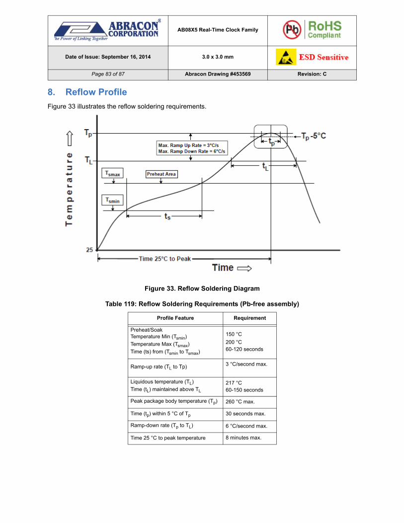
AB08X5 Real-Time Clock Family
Date of Issue: September 16, 2014 3.0 x 3.0 mm
Page 83 of 87 Abracon Drawing #453569 Revision: C
8. Reflow Profile
Figure 33 illustrates the reflow soldering requirements.
Figure 33. Reflow Soldering Diagram
Table 119: Reflow Soldering Requirements (Pb-free assembly)
Profile Feature Requirement
Preheat/SoakTemperature Min (Tsmin)
Temperature Max (Tsmax)
Time (ts) from (Tsmin to Tsmax)
150 °C
200 °C60-120 seconds
Ramp-up rate (TL to Tp) 3 °C/second max.
Liquidous temperature (TL)
Time (tL) maintained above TL
217 °C60-150 seconds
Peak package body temperature (Tp) 260 °C max.
Time (tp) within 5 °C of Tp 30 seconds max.
Ramp-down rate (Tp to TL) 6 °C/second max.
Time 25 °C to peak temperature 8 minutes max.

AB08X5 Real-Time Clock Family
Date of Issue: September 16, 2014 3.0 x 3.0 mm
Page 84 of 87 Abracon Drawing #453569 Revision: C
9. Ordering Information
Table 120: Ordering Information
AB08X5 Orderable Part Numbers Package
Temperature Range MSL Level(2)
P/N Tape and Reel Qty
AB0805-T3 3000pcs/reel Pb-Free(1) 16-Pin QFN 3 x 3 mm
-40 to +85 °C 1AB0815-T3 3000pcs/reel
(1) Compliant and certified with the current RoHS requirements for all 6 substances, including the requirement that lead not exceed 0.1% by weight in raw homogeneous materials. The package was designed to be soldered at high temperatures (per reflow profile) and can be used in specified lead-free processes.
(2) Moisture Sensitivity Level rating according to the JEDEC J-STD-020D.1 industry standard classifications.

AB08X5 Real-Time Clock Family
Date of Issue: September 16, 2014 3.0 x 3.0 mm
Page 85 of 87 Abracon Drawing #453569 Revision: C
10. ABRACON CORPORATION – TERMS & CONDITIONS OF SALE
The following are the terms and conditions under which Abracon Corporation (“AB”) agrees to sell, to theentity named on the face hereof (“Buyer”), the products specified on the face hereof (the “Products”).Notwithstanding Buyer’s desire to use standardized RFQs, purchase order forms, order forms,acknowledgment forms and other documents which may contain terms in addition to or at variance withthese terms, it is expressly understood and agreed that other forms shall neither add to, nor vary, theseterms whether or not these terms are referenced therein. Buyer may assent to these terms by writtenacknowledgment, implication and/or by acceptance or payment of goods ordered any of which willconstitute assent.
1. Prices: Prices shown on the face hereof are in US dollars, with delivery terms specified herein andare exclusive of any other charges including, without limitation, fees for export, special packaging,freight, insurance and similar charges. AB reserves the right to increase the price of Products by writ-ten notice to Buyer at least thirty (30) days prior to the original date of shipment. When quantity pricediscounts are quoted by AB, the discounts are computed separately for each type of product to besold and are based upon the quantity of each type and each size ordered at any one time. If any dis-counted order is reduced by Buyer with AB’s consent, the prices shall be adjusted to the higher prices,if applicable, for the remaining order.
2. Taxes: Unless otherwise specified in the quotation, the prices do not include any taxes, import orexport duties, tariffs, customs charges or any such other levies. Buyer agrees to reimburse AB theamount of any federal, state, county, municipal, or other taxes, duties, tariffs, or custom charges AB isrequired to pay. If Buyer is exempt from any such charges, Buyer must provide AB with appropriatedocumentation.
3. Payment Terms: For each shipment, AB will invoice Buyer for the price of the Products plus all appli-cable taxes, packaging, transportation, insurance and other charges. Unless otherwise stated in aseparate agreement or in AB’s quotation, payments are due within thirty (30) days from the date ofinvoice, subject to AB’s approval of Buyer’s credit application. All invoicing disputes must be submit-ted in writing to AB within ten (10) days of the receipt of the invoice accompanied by a reasonablydetailed explanation of the dispute. Payment of the undisputed amounts shall be made timely. ABreserves the right to require payment in advance or C.O.D. and otherwise modified credit terms.When partial shipments are made, payments for such shipments shall become due in accordancewith the above terms upon submission of invoices. If, at the request of Buyer, shipment is postponedfor more than thirty (30) days, payment will become due thirty days after notice to Buyer that Productsare ready for shipment. Any unpaid due amounts will be subject to interest at one decimal five per-cent (1.5%) per month, or, if less, the maximum rate allowed by law.
4. Delivery and Shipment: Shipment dates are estimates only. Failure to deliver by a specified dateshall neither entitle Buyer to any compensation nor impose any liability on AB. AB reserves the rightto ship and bill ten percent more or less than the exact quantity specified on the face hereof. All ship-ments will be made Ex Works as per Incoterms 2000 from AB’s place of shipment. In the absence ofspecific instructions, AB will select the carrier. Claims against AB for shortages must be made in writ-ing within ten (10) days after the arrival of the shipment. AB is not required to notify Buyer of the ship-ment. Buyer shall pay all freight charges, insurance and other shipping expenses. Freight charges,insurance and other shipping expenses itemized in advance of actual shipment, if any, are estimatesonly that are calculated on the basis of standard tariffs and may not reflect actual costs. Buyer mustpay actual costs.
5. Purchase Order Changes and Cancellations: Purchase orders for standard AB Products may notbe canceled within sixty (60) days of the original shipping date. Purchase orders for non-standard ABProducts are non-cancelable and non-returnable. All schedule changes must be requested at leastthirty (30) days prior to original shipping date. Maximum schedule change “push-out” shall be nomore than thirty (30) days from original shipping date. AB may terminate or cancel this order, in wholeor in part, at any time prior to the completion of performance by written notice to Buyer without incur-

AB08X5 Real-Time Clock Family
Date of Issue: September 16, 2014 3.0 x 3.0 mm
Page 86 of 87 Abracon Drawing #453569 Revision: C
ring any liability to Buyer for breach of contract or otherwise. AB reserves the right to allocate Prod-ucts in its sole discretion among Buyer and other potential buyers, or defer or delay the shipment ofany Product, which is in short supply due to any reason.
6. Title and Risk of Loss: AB’s responsibility for any loss or damage ends, and title passes, whenProducts are delivered Ex Works as per Incoterms 2000 at AB’s designated shipping location to car-rier, to Buyer or to Buyer’s agent, whichever occurs first.
7. Packing: Packaging shall be AB’s standard shipping materials or as specified on the face hereof.Any cost of non-standard packaging and handling requested by Buyer shall be abided by AB providedBuyer gives reasonable prior notice and agrees in writing to pay additional costs.
8. Security Interest: Buyer hereby grants AB a purchase money security interest in the Products soldand in the proceeds of resale of such Products until such time as Buyer has paid all charges. ABretains all right and remedies available to AB under the Uniform Commercial Code.
9. Specifications: Specifications for each Product are the specifications specified in the published data-sheets of such Product, as of the date of AB’s quotation (the “Specifications”). Except as otherwiseagreed, AB reserves the right to modify the Specifications at any time without adversely affecting thefunctionality.
10. Acceptance: Unless Buyer notifies AB in writing within ten (10) days from the date of receipt of Prod-ucts that the Products fail to conform to the Specifications, the Products will be deemed accepted byBuyer. No such claim of non-conformity shall be valid if (i) the Products have been altered, modifiedor damaged by Buyer, (ii) the rejection notice fails to explain the non-conformance in reasonable detailand is not accompanied by a test report evidencing the non-conformity, or (iii) rejected Products arenot returned to AB within thirty (30) days of rejection; provided, that no Product returns may be madewithout a return material authorization issued by AB.
11. Limited Warranties and Disclaimers: AB warrants to Buyer that each Product, for a period of twelve(12) months from shipment date thereof, will conform to the Specifications and be free from defects inmaterials and workmanship. AB’s sole liability and Buyer’s exclusive remedy for Products that fail toconform to this limited warranty (“Defective Products”) is limited to repair or replacement of suchDefective Products, or issue a credit or rebate of no more than the purchase price of such DefectiveProducts, at AB’s sole option and election. This warranty shall not apply: (i) if Products have beendamaged or submitted to abnormal conditions (mechanical, electrical, or thermal) during transit, stor-age, installation, or use; or (ii) if Products are subject to Improper Use (as defined below); or (iii) if thenon-conformance of Products results from misuse, neglect, improper testing, storage, installation,unauthorized repair, alteration, or excess usage at or beyond the maximum values (temperature limit,maximum voltage, and other Specification limits) defined by AB; (iv) to any other default not attribut-able to AB; or (v) removal, alteration, or tampering of the original AB product labeling. This warrantydoes not extend to Products or components purchased from entities other than AB or AB’s authorizeddistributors or to third-party software or documentation that may be supplied with any Product. In theevent no defect or breach of warranty is discovered by AB upon receipt of any returned Product, suchProduct will be returned to Buyer at Buyer’s expense and Buyer will reimburse AB for the transporta-tion charges, labor, and associated charges incurred in testing the allegedly Defective Product. Theabove warranty is for Buyer’s benefit only, and is non-transferable. OTHER THAN THE LIMITEDWARRANTY SET FORTH ABOVE, AB MAKES NO WARRANTIES, EXPRESS, STATUTORY,IMPLIED, OR OTHERWISE AND SPECIFICALLY DISCLAIMS THE IMPLIED WARRANTIES OFMERCHANTABILITY, FITNESS FOR A PARTICULAR PURPOSE AND NON-INFRINGEMENT, TOTHE MAXIMUM EXTENT PERMITTED BY LAW. WITHOUT LIMITING THE GENERALITY OF THEFOREGOING DISCLAIMERS, AB INCORPORATES BY REFERENCE ANY PRODUCT-SPECIFICWARRANTY DISCLAIMERS SET FORTH IN THE PUBLISHED PRODUCT DATASHEETS.
12. Limitation of Liability: AB SHALL HAVE NO LIABILITY FOR LOSS ARISING FROM ANY CLAIMMADE AGAINST BUYER, OR FOR SPECIAL, INDIRECT, RELIANCE, INCIDENTAL, CONSEQUEN-TIAL, OR PUNITIVE DAMAGES INCLUDING, WITHOUT LIMITATION, LOSS OF USE, PROFITS,REVENUES, OR COST OF PROCUREMENT OF SUBSTITUTE GOODS BASED ON ANY BREACH

AB08X5 Real-Time Clock Family
Date of Issue: September 16, 2014 3.0 x 3.0 mm
Page 87 of 87 Abracon Drawing #453569 Revision: C
OR DEFAULT OF AB, HOWEVER CAUSED, AND UNDER ANY THEORY OF LIABILITY. BUYER’SSOLE REMEDY AND AB’S SOLE AND TOTAL LIABILITY FOR ANY CAUSE OF ACTION,WHETHER IN CONTRACT (INCLUDING BREACH OF WARRANTY) OR TORT (INCLUDING NEG-LIGENCE OR MISREPRESENTATION) OR UNDER STATUTE OR OTHERWISE SHALL BE LIM-ITED TO AND SHALL NOT EXCEED THE AGGREGATE AMOUNTS PAID BY BUYER TO AB FORPRODUCTS WHICH GIVE RISE TO CLAIMS. BUYER SHALL ALWAYS INFORM AB OF ANYBREACH AND AFFORD AB REASONABLE OPPORTUNITY TO CORRECT ANY BREACH. THEFOREGOING LIMITATIONS SHALL APPLY REGARDLESS OF WHETHER AB HAS BEENADVISED OF THE POSSIBILITY OF SUCH DAMAGES AND NOTWITHSTANDING THE FAILUREOF ESSENTIAL PURPOSE OF ANY LIMITED REMEDY.
13. Improper Use: Buyer agrees and covenants that, without AB’s prior written approval, Products willnot be used in life support systems, human implantation, nuclear facilities or systems or any otherapplication where Product failure could lead to loss of life or catastrophic property damage (each suchuse being an “Improper Use”). Buyer will indemnify and hold AB harmless from any loss, cost, ordamage resulting from Improper Use of the Products.
14. Miscellaneous: In the event of any insolvency or inability to pay debts as they become due by Buyer,or voluntary or involuntary bankruptcy proceeding by or against Buyer, or appointment of a receiver orassignee for the benefit of creditors of Buyer, AB may elect to cancel any unfulfilled obligations. NoProducts or underlying information or technology may be exported or re-exported, directly or indi-rectly, contrary to US law or US Government export controls. AB will be excused from any obligationto the extent performance thereof is caused by, or arises in connection with, acts of God, fire, flood,riots, material shortages, strikes, governmental acts, disasters, earthquakes, inability to obtain laboror materials through its regular sources, delay in delivery by AB’s supplies or any other reason beyondthe reasonable control of AB. In the event any one or more of the provisions contained herein shall forany reason be held to be invalid, illegal, or unenforceable in any respect, such invalidity, illegality, orunenforceability shall not affect any other provision hereof and these terms shall be construed as ifsuch invalid, illegal, or unenforceable provision had never been contained herein. A waiver of abreach or default under these terms shall not be a waiver of any subsequent default. Failure of AB toenforce compliance with any of these terms shall not constitute a waiver of such terms. These termsare governed by the laws of the State of California without reference to conflict of law principles. Thefederal and state courts located within the State of California will have exclusive jurisdiction to adjudi-cate any dispute arising out of these terms.
END