solution to the e-beam gate resist blistering problem of 0 ... · a simple screening apparatus has...
TRANSCRIPT
Solution to the E-beam Gate Resist BlisteringProblem of 0.15 micron PHEMTs
Y.C. Pao, K. Tran, C. Shih, N. HardyFiltronic Solid State, Inc., 3251 Olcott Street, Santa Clara, CA 95054
Copyright © 1999 GaAs Mantech
AbstractIn this paper we report a simple solution to the E-beam
gate resist blistering problem encountered during the
Ti/Pt/Au metallization. This has been one of the major
yield concerns when manufacturing quarter micron or sub
quarter micron PHEMTs. A free space screening method
has been successfully used to eliminate the PMMA based
E-beam resist blisters during the gate metal deposition
process.
Introduction
It is common for PMMA based photoresist, used for E-
beam direct write processing, to blister during the e-beam
metal evaporation of Ti/Pt/Au based 0.15 and 0.25 micron
gate. This problem has been speculated [1] to be due to X-
ray irradiation, substrate heating, or free electron
bombardment. In this study, we will show evidence that the
resist blistering problem is mainly due to the excess
electron charging effect during refractory metal gate
evaporation. This free electron charging affects the PMMA
resist chemistry, causing gas outburst to make the resist
blistered. Experiments were carried out with wafers coated
with PMMA on the bottom and MMA(17.5)MAA EL on
the top. All metal evaporations were done in a commercial
Temescal E-beam evaporator. The gate metal consists of
three layers: titanium, platinum, and gold with a total
thickness ranging from 3500 to 5000 angstroms. From the
test results, it has been demonstrated that the evaporation
of the platinum layer is the source of excess electrons
leading to resist charging, hence causing chemical reaction
in the resist and evolving chemically reacted gas. The gas
trapped under the titanium layer caused bubbles and
eventually blistered the metal and resist layers.
A simple screening apparatus has been developed and
implemented to eliminate the electron charging effect
during the E-beam gate metallization. Details of the
experiment and the construction of the screening apparatus
will be discussed in this paper.
Experiments and results
The photoresist blistering experiment was carried out
in two different Temescal models of E-beam evaporators
with standard gate metal composition of Ti/Pt/Au. Both
systems are equipped with the same 10 KV e-guns. All
experiments were conducted with fixed metal deposition
rates of 3 angstroms/sec for titanium, 2 angstroms/sec for
platinum, and 10 angstroms/sec for gold.
The wafers are first coated with PMMA on the bottom
and MMA(17.5)MAA EL on the top. After E-beam direct
write exposure to form the gate patterns, the resist was
then developed and baked to form the desired cross
sectional profile. After the selective gate recess etch, the
wafer was loaded into the e-beam evaporation system.
Typical operation pressure is below 1E-6 torr. After the
Ti/Pt/Au metal evaporation, resist peeling at different
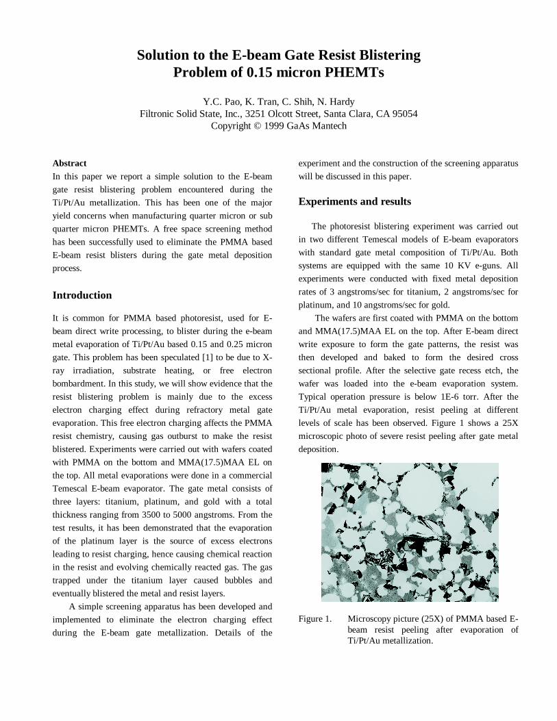
levels of scale has been observed. Figure 1 shows a 25X
microscopic photo of severe resist peeling after gate metal
deposition.
Figure 1. Microscopy picture (25X) of PMMA based E-beam resist peeling after evaporation ofTi/Pt/Au metallization.
It is speculated that the resist peeling may be caused
by thermal, electron or x-ray radiation [1]. Due to the fact
that the metal evaporation is performed with a high voltage
e-gun, it is most likely the radiation does come from the
free electrons inside the e-beam evaporation chamber.
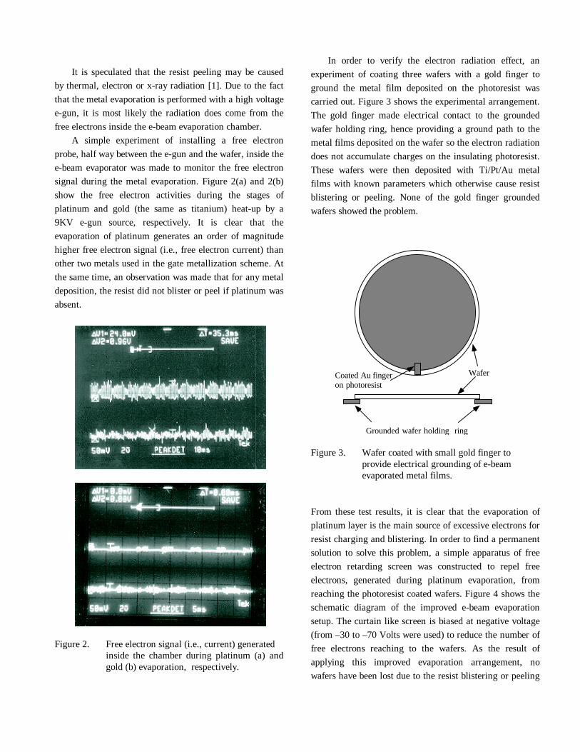
A simple experiment of installing a free electron
probe, half way between the e-gun and the wafer, inside the
e-beam evaporator was made to monitor the free electron
signal during the metal evaporation. Figure 2(a) and 2(b)
show the free electron activities during the stages of
platinum and gold (the same as titanium) heat-up by a
9KV e-gun source, respectively. It is clear that the
evaporation of platinum generates an order of magnitude
higher free electron signal (i.e., free electron current) than
other two metals used in the gate metallization scheme. At
the same time, an observation was made that for any metal
deposition, the resist did not blister or peel if platinum was
absent.
Figure 2. Free electron signal (i.e., current) generatedinside the chamber during platinum (a) andgold (b) evaporation, respectively.
In order to verify the electron radiation effect, an
experiment of coating three wafers with a gold finger to
ground the metal film deposited on the photoresist was
carried out. Figure 3 shows the experimental arrangement.
The gold finger made electrical contact to the grounded
wafer holding ring, hence providing a ground path to the
metal films deposited on the wafer so the electron radiation
does not accumulate charges on the insulating photoresist.
These wafers were then deposited with Ti/Pt/Au metal
films with known parameters which otherwise cause resist
blistering or peeling. None of the gold finger grounded
wafers showed the problem.
Figure 3. Wafer coated with small gold finger toprovide electrical grounding of e-beamevaporated metal films.
From these test results, it is clear that the evaporation of
platinum layer is the main source of excessive electrons for
resist charging and blistering. In order to find a permanent
solution to solve this problem, a simple apparatus of free
electron retarding screen was constructed to repel free
electrons, generated during platinum evaporation, from
reaching the photoresist coated wafers. Figure 4 shows the
schematic diagram of the improved e-beam evaporation
setup. The curtain like screen is biased at negative voltage
(from –30 to –70 Volts were used) to reduce the number of
free electrons reaching to the wafers. As the result of
applying this improved evaporation arrangement, no
wafers have been lost due to the resist blistering or peeling
Coated Au fingeron photoresist
Wafer
Grounded wafer holding ring

problems during the Ti/Pt/Au based 0.15 and 0.25 micron
PHEMT gate metallization.
Figure 4. Schematic diagram of the free electronretarding screen used during the e-beamevaporation of Ti/Pt/Au based metallization.
Conclusion
The problem of PMMA based E-beam resist blisters
during the e-beam gate metallization has been studied. The
problem is mainly due to excess electron charging effect
during refractory metal (or to be more specific the
platinum) gate evaporation. The free electron charging
effect during the platinum deposition affects the PMMA
resist chemistry, causing reacted gas to outburst under
vacuum. Since the gas is trapped under the titanium and
platinum layers, this causes bubbles and eventually breaks
through the metal and resist layers to create resist peeling,
which is shown in Figure 1.
From experimental results, it is further demonstrated
that there are two possible ways to prevent the E-beam
photoresist blistering and peeling problem; one is to
ground the coated wafer surface, the other is to repel free
electrons before they reach the processed wafers. A simple
screening apparatus has been developed and implemented
to eliminate the electron charging effect during the E-beam
gate metallization. This method has been proven to be very
effective to solve the E-beam photoresist blistering and
peeling problem.
Acknowledgments
The authors wish to thank J. Franklin, S. Ratcliff, and
T. Mirra for useful technical discussions.
References
[1] D. Kuhn, K. Prutt, A. Kashiwagi, J. Peterson, K. Yamamoto,L. Studebaker, S. Lafrancois, N. Caldwell, “E-beam MetalEvaporation: Photoresist Critical Dimensions & SubstrateAdhesion Dependence on Throw Distance, Deposition Rate,Radiation, and Film Stress”, Proceeding of 1998 MANTECHConference, p.213, 1998.
-V-V
Target E-gun
Wafer
e-
e-
-----
-----