solo-1 pci audiodrive solution data sheet - hardware secrets · preliminarysolo-1tm pci...
TRANSCRIPT

ESS Technology, Inc. SAM0090-012398 1
PRELIMINARY Solo-1 TM
PCI AudioDrive® SolutionData Sheet
DESCRIPTION
The Solo-1TM PCI AudioDrive® solution implements a single-chip PCI audio solution, providing high-quality audioprocessing while maintaining full legacy DOS gamecompatibility. With a dynamic range over 80 dB, the Solo-1complies with the Microsoft® PC 97/PC 98 specificationsand meets WHQL audio requirements. The Solo-1 forms acomplete audio subsystem on a single chip for both add-incard and motherboard platforms.
The Solo-1 incorporates a microcontroller, ESFMTM musicsynthesizer, 3-D stereo effects processor, 16-bit stereowave ADC and DAC, 16-bit stereo music DAC, MPU-401UART mode serial port, dual game port, hardware mastervolume control, a serial port interface to externalwavetable music synthesizer, DMA control logic withFIFO, and PCI bus interface logic. There are three stereoinputs (typically line-in, CD audio, and auxiliary line) and amono microphone input.
The Solo-1 integrates ESS’ field-proven hardware designfor DOS game compatibility with hardware FM synthesis(ESFM) and three methods for legacy audio controlinterface: PC/PCI, Distributed DMA, and TransparentDMA. Transparent DMA requires no sideband signalsfrom PC core logic chipsets in addition to the standard PCI2.1 bus. TDMA is compatible with Pentium®, PentiumPro®, and Pentium® II chipsets as well as standard PCIadd-in cards.
The Solo-1 can record, compress, and play back voice,sound, and music with built-in mixer controls. It supportsstereo full-duplex operation for simultaneous record andplayback. The ESFM synthesizer has extendedcapabilities within native mode operation providingsuperior sound and power-down capabilities.
The integrated 3-D audio effects processor usestechnology from Spatializer® Audio Laboratories, Inc. andexpands the sound field emitted by two speakers to createa resonant 3-D sound environment.
The Solo-1 is compliant with Advanced Configuration andPower Interface (ACPI) standards.
It is available in an industry-standard 100-pin Thin QuadFlat Pack (TQFP) package.
FEATURES
• Single, high-performance, mixed-signal, 16-bit stereo VLSI chip
• PCI bus specification, revision 2.1
• Full native DOS games compatibility, via three technologies:
– TDMA – DDMA – PC/PCI
• High-Quality ESFM music synthesizer
• Dynamic range (SNR) over 80 dB
• Integrated Spatializer® 3-D audio effects processor
Record and Playback Features • Record, compress, and play back voice, sound, and music
• 16-Bit stereo ADC and DAC
• Programmable independent sample rates from 4 kHz up to 48 kHz for record and playback
• Full-Duplex operation for simultaneous record and playback
• 2-Wire hardware volume control for up, down, and mute
Inputs and Outputs • Stereo inputs for line-in, auxiliary A (CD audio), and
auxiliary B, and a mono input for microphone
• MPU-401 (UART mode) interface for wavetable synthesizers and MIDI devices
• Integrated dual game port
• Separate mono input (MONO_IN) and mono output (MONO_OUT) for speakerphone
Mixer Features • 8-Channel mixer with stereo inputs for line, CD audio,
auxiliary line, music synthesizer, digital audio (wave files), and mono inputs for microphone and speakerphone
• Programmable 6-bit logarithmic master volume control
Power • Advanced power management meets ACPI standards
• Supports 5.0 V operation
Compatibility • Supports PC games and applications for Sound BlasterTM
and Sound BlasterTM Pro
• Supports Microsoft® WindowsTM Sound System®
• Meets PC 97/PC 98 and WHQL specifications
2 SAM0090-012398 ESS Technology, Inc.
SOLO-1 DATA SHEET
FEATURESPRELIMINARY
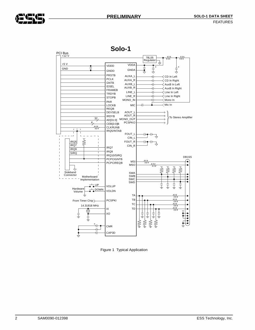
Figure 1 Typical Application
AOUT_L
LINE_R
LINE_L
CIN_R
CIN_LFOUT_L
FOUT_R
VDDA
GNDA
MIC
CMR
AUXA_R
AUXA_L
SWASWBSWCSWD
PRSTB
IRQ7
GNDD
IRQ5/INTAB
TA
TB
TC
TD
REQB
CEB[3:0]B
LOCKB
AD[31:0]
PAR
IRDYB
TRDYBFRAMEBIDSELGNTBPCLK
IRQ9IRQ10/SIRQ
AOUT_R
VDDD
MSOMSI
+12 V78L05
Regulator
CD In LeftCD In RightAuxB In LeftAuxB In RightLine In LeftLine In Right
AUXB_RAUXB_L
Mic In
To Stereo Amplifier
DB15S
+5 V
GND
Solo-1PCI Bus
STOPB
XI
XO
14.31818 MHz
DEVSELB
CLKRUNB
CAP3D
MONO_OUTPCSPKO
MONO_IN Mono In
+ +
PCSPKIFrom Timer Chip
UP
DOWN VOLDN
VOLUPHardwareVolume
32
4
+
PCPCIGNTBPCPCIREQB
Sideband
IRQ7IRQ9SIRQ
MotherboardImplementation
IRQ5
Connector

ESS Technology, Inc. SAM0090-012398 3
SOLO-1 DATA SHEET
CONTENTSPRELIMINARY
CONTENTS
DESCRIPTION . . . . . . . . . . . . . . . . . . . . . . . . . . . . . . . . . . . . 1FEATURES . . . . . . . . . . . . . . . . . . . . . . . . . . . . . . . . . . . . . . . 1PINOUT . . . . . . . . . . . . . . . . . . . . . . . . . . . . . . . . . . . . . . . . . 5PIN DESCRIPTION . . . . . . . . . . . . . . . . . . . . . . . . . . . . . . . . 6FUNCTIONAL DESCRIPTION . . . . . . . . . . . . . . . . . . . . . . . . 8
Digital Subsystems . . . . . . . . . . . . . . . . . . . . . . . . . . . . . 9Analog Subsystems . . . . . . . . . . . . . . . . . . . . . . . . . . . . . 9
MIXER SCHEMATIC BLOCK DIAGRAM . . . . . . . . . . . . . . . 10BUS INTERFACING . . . . . . . . . . . . . . . . . . . . . . . . . . . . . . . 11DIGITAL AUDIO . . . . . . . . . . . . . . . . . . . . . . . . . . . . . . . . . . 12
Data Formats . . . . . . . . . . . . . . . . . . . . . . . . . . . . . . . . . 12Audio 1 DMA Transfers in SB Compatibility Mode . 12Audio 1 DMA Transfers in Extended Mode . . . . . . 13Audio 1 DMA Transfers in Native PCI Mode . . . . . 13Data Transfers Using the Second Audio Channel . 13
First DMA Channel CODEC . . . . . . . . . . . . . . . . . . . . . 14INTERRUPTS . . . . . . . . . . . . . . . . . . . . . . . . . . . . . . . . . . . . 15
Interrupt Status Register . . . . . . . . . . . . . . . . . . . . . . . . 15Interrupt Mask Register . . . . . . . . . . . . . . . . . . . . . . . . . 15
PERIPHERAL INTERFACING . . . . . . . . . . . . . . . . . . . . . . . 16Wavetable Interface . . . . . . . . . . . . . . . . . . . . . . . . . . . . 16Joystick / MPU-401 Interface . . . . . . . . . . . . . . . . . . . . . 16
MPU-401 UART Mode . . . . . . . . . . . . . . . . . . . . . . 16Joystick / MIDI External Interface . . . . . . . . . . . . . . 16
MONO_IN and MONO_OUT . . . . . . . . . . . . . . . . . . . . . 17Spatializer Audio Processor . . . . . . . . . . . . . . . . . . . . . . 17Hardware and Master Volume Control . . . . . . . . . . . . . 18PC Speaker . . . . . . . . . . . . . . . . . . . . . . . . . . . . . . . . . . 18
PC Speaker Volume Control . . . . . . . . . . . . . . . . . 18ANALOG DESIGN CONSIDERATIONS . . . . . . . . . . . . . . . . 19
Game Port . . . . . . . . . . . . . . . . . . . . . . . . . . . . . . . . . . . 19Reference Generator . . . . . . . . . . . . . . . . . . . . . . . . . . . 19Switched-Capacitor Filter . . . . . . . . . . . . . . . . . . . . . . . . 19Audio Inputs and Outputs . . . . . . . . . . . . . . . . . . . . . . . 19
PCI CONFIGURATION REGISTERS . . . . . . . . . . . . . . . . . . 20Register Summary . . . . . . . . . . . . . . . . . . . . . . . . . . . . . 20Register Descriptions . . . . . . . . . . . . . . . . . . . . . . . . . . . 21
I/O PORTS . . . . . . . . . . . . . . . . . . . . . . . . . . . . . . . . . . . . . . 27Port Summary . . . . . . . . . . . . . . . . . . . . . . . . . . . . . . . . 27Port Descriptions . . . . . . . . . . . . . . . . . . . . . . . . . . . . . . 28
IO Device . . . . . . . . . . . . . . . . . . . . . . . . . . . . . . . . 28Audio/FM Device . . . . . . . . . . . . . . . . . . . . . . . . . . 28MPU-401 Device . . . . . . . . . . . . . . . . . . . . . . . . . . 31Game Port Device . . . . . . . . . . . . . . . . . . . . . . . . . 31DMAC Device . . . . . . . . . . . . . . . . . . . . . . . . . . . . . 32
PROGRAMMING THE SOLO-1 . . . . . . . . . . . . . . . . . . . . . . 33Identifying the Solo-1 . . . . . . . . . . . . . . . . . . . . . . . . . . . 33Resetting and Initializing the Solo-1 . . . . . . . . . . . . . . . 33Programming for DOS Game Compatibility . . . . . . . . . . 34Selecting DMA/IRQ Policy . . . . . . . . . . . . . . . . . . . . . . . 34Programming for Native PCI Audio . . . . . . . . . . . . . . . . 35
Configuring Audio 1 in Native Mode . . . . . . . . . . . . 35
Configuring Audio 2 in Native Mode . . . . . . . . . . . . 35Modes of Operation . . . . . . . . . . . . . . . . . . . . . . . . . . . . 35
Compatibility Mode Description . . . . . . . . . . . . . . . . 35Extended Mode Description . . . . . . . . . . . . . . . . . . 35Mixing Modes Not Recommended . . . . . . . . . . . . . 36
Data Formats . . . . . . . . . . . . . . . . . . . . . . . . . . . . . . . . . 36Compressed Data Formats . . . . . . . . . . . . . . . . . . . 36Sound Blaster Pro Compatible Data Formats . . . . . 36Stereo DMA Transfers in Compatibility Mode . . . . . 36Solo-1 Data Formats (Extended Mode and Audio 2) 37Sending Commands During DMA Operations . . . . 37
Compatibility Mode Programming . . . . . . . . . . . . . . . . . 37Compatibility Mode DAC Operation . . . . . . . . . . . . 37Compatibility Mode ADC Operation . . . . . . . . . . . . 38
Extended Mode Programming . . . . . . . . . . . . . . . . . . . . 39Commanding Solo-1 Controller Registers . . . . . . . . 39Solo-1 Command/Data Handshaking Protocol . . . . 39Extended Mode Audio 1 DAC Operation . . . . . . . . 40Extended Mode Audio 1 ADC Operation . . . . . . . . 41Extended Mode Programmed I/O Operation . . . . . . 43Second Audio Channel DAC Operation . . . . . . . . . 43
Programming the Solo-1 Mixer . . . . . . . . . . . . . . . . . . . . 45Writing and Reading Data from the Mixer Registers 45Resetting the Mixer Registers . . . . . . . . . . . . . . . . . 45Extended Access to SB Pro Mixer Volume Controls 46Extended Access to Mic Mix Volume . . . . . . . . . . . 46Extended Access to ADC Source Select . . . . . . . . 46Sound Blaster Pro Volume Emulation . . . . . . . . . . . 47Record and Playback Mixer . . . . . . . . . . . . . . . . . . 48
REGISTERS . . . . . . . . . . . . . . . . . . . . . . . . . . . . . . . . . . . . . 49Register Types . . . . . . . . . . . . . . . . . . . . . . . . . . . . . . . . 49
Types of Register Access . . . . . . . . . . . . . . . . . . . . 49Mixer Registers . . . . . . . . . . . . . . . . . . . . . . . . . . . . 49Controller Registers . . . . . . . . . . . . . . . . . . . . . . . . 58Controller Register Descriptions . . . . . . . . . . . . . . . 59
AUDIO MICROCONTROLLER COMMAND SUMMARY . . . 63POWER MANAGEMENT . . . . . . . . . . . . . . . . . . . . . . . . . . . 65
CLKRUN Protocol . . . . . . . . . . . . . . . . . . . . . . . . . . . . . 65PCI Power Management Interface (PPMI) . . . . . . . . . . . 65
ELECTRICAL CHARACTERISTICS . . . . . . . . . . . . . . . . . . . 66Absolute Maximum Ratings . . . . . . . . . . . . . . . . . . . . . . 66Thermal Characteristics . . . . . . . . . . . . . . . . . . . . . . . . . 66Operating Conditions . . . . . . . . . . . . . . . . . . . . . . . . . . . 66Operating Current (Typical) . . . . . . . . . . . . . . . . . . . . . . 66
TIMING DIAGRAMS . . . . . . . . . . . . . . . . . . . . . . . . . . . . . . . 68TIMING CHARACTERISTICS . . . . . . . . . . . . . . . . . . . . . . . . 69MECHANICAL DIMENSIONS . . . . . . . . . . . . . . . . . . . . . . . . 70APPENDIX A: ES689/ES69X DIGITAL SERIAL INTERFACE 71APPENDIX B: SCHEMATICS . . . . . . . . . . . . . . . . . . . . . . . . 72APPENDIX C: BILL OF MATERIALS . . . . . . . . . . . . . . . . . . 76APPENDIX D: LAYOUT GUIDELINES . . . . . . . . . . . . . . . . . 78
4 SAM0090-012398 ESS Technology, Inc.
SOLO-1 DATA SHEET
FIGURESPRELIMINARY
FIGURES
Figure 1 Typical Application . . . . . . . . . . . . . . . . . . . . . . . . . .2Figure 2 Solo-1 Pinout . . . . . . . . . . . . . . . . . . . . . . . . . . . . . .5Figure 3 Solo-1 Block Diagram . . . . . . . . . . . . . . . . . . . . . . . .8Figure 4 Solo-1 Mixer Schematic Block Diagram . . . . . . . . .10Figure 5 Data Transfer Modes . . . . . . . . . . . . . . . . . . . . . . .12Figure 6 Dual Joystick/MIDI Connector . . . . . . . . . . . . . . . . .16Figure 7 MIDI Serial Interface . . . . . . . . . . . . . . . . . . . . . . . .17Figure 8 PC Speaker Volume Circuitry . . . . . . . . . . . . . . . . .18Figure 9 Reference Generator Pin Diagram . . . . . . . . . . . . .19Figure 10 Switched-Capacitor Filter Pin Diagram . . . . . . . . .19Figure 11 Command Transfer Timing . . . . . . . . . . . . . . . . . .37
Figure 12 PCLK Timing . . . . . . . . . . . . . . . . . . . . . . . . . . . . 68Figure 13 PRST Timing . . . . . . . . . . . . . . . . . . . . . . . . . . . . 68Figure 14 PCI Signal Timing . . . . . . . . . . . . . . . . . . . . . . . . 68Figure 15 Solo-1 Mechanical Dimensions . . . . . . . . . . . . . . 70Figure 16 Solo-1 Schematic . . . . . . . . . . . . . . . . . . . . . . . . 72Figure 17 ES692 Schematic . . . . . . . . . . . . . . . . . . . . . . . . 73Figure 18 Amplifier . . . . . . . . . . . . . . . . . . . . . . . . . . . . . . . . 74Figure 19 PC Interface . . . . . . . . . . . . . . . . . . . . . . . . . . . . . 75Figure 20 Analog Components on One Side of the PCB . . . 78Figure 21 Analog Components on Both Sides of the PCB . 78
TABLES
Table 1 PCI Bus Interface Pins . . . . . . . . . . . . . . . . . . . . . . . 11Table 2 Extended Mode Audio 1 Controller Registers . . . . .13Table 3 Audio 2 Related Mixer Registers . . . . . . . . . . . . . . .14Table 4 Solo-1 Interrupt Sources . . . . . . . . . . . . . . . . . . . . . .15Table 5 Interrupt Status Bits in IOBase+7h . . . . . . . . . . . . . .15Table 6 Wavetable Interface Pins . . . . . . . . . . . . . . . . . . . . .16Table 7 PCI Configuration Registers Summary . . . . . . . . . . .20Table 8 Supported Legacy Audio Addresses . . . . . . . . . . . .24Table 9 I/O Port Summary . . . . . . . . . . . . . . . . . . . . . . . . . . .27Table 10 Hardware and Software Reset Initializations . . . . .33Table 11 ISA DMA Policy Bits for Add-On Cards . . . . . . . . .34Table 12 ISA DMA Policy Bits for Motherboards . . . . . . . . . .34Table 13 ISA IRQ Emulation Policy Bits . . . . . . . . . . . . . . . .34Table 14 Comparison of Operation Modes . . . . . . . . . . . . . .36Table 15 Uncompressed DAC Transfer Modes . . . . . . . . . . .38Table 16 Uncompressed ADC Transfer Modes . . . . . . . . . . .39
Table 17 Command Sequences for DMA Playback . . . . . . . 41Table 18 Command Sequence for DMA Record . . . . . . . . . 42Table 19 Sound Blaster Pro/Extended Access Registers . . 46Table 20 SB Pro Read Volume Emulation . . . . . . . . . . . . . . 47Table 21 SB Pro Write Volume Emulation . . . . . . . . . . . . . . 47Table 22 Extended Access Mixer Volume Values . . . . . . . . 48Table 23 Mixer Input Volume Registers . . . . . . . . . . . . . . . . 48Table 24 Sound Blaster Compatibility Register Summary . . 49Table 25 ESS Mixer Registers Summary . . . . . . . . . . . . . . . 50Table 26 ESS Controller Registers Summary . . . . . . . . . . . 58Table 27 Command Summary . . . . . . . . . . . . . . . . . . . . . . . 63Table 28 Digital Characteristics . . . . . . . . . . . . . . . . . . . . . . 66Table 29 Analog Characteristics . . . . . . . . . . . . . . . . . . . . . 67Table 30 Timing Characteristics . . . . . . . . . . . . . . . . . . . . . . 69Table 31 Solo-1 Bill of Materials (BOM) . . . . . . . . . . . . . . . . 76
ESS Technology, Inc. SAM0090-012398 5
SOLO-1 DATA SHEET
PINOUTPRELIMINARY
PINOUT
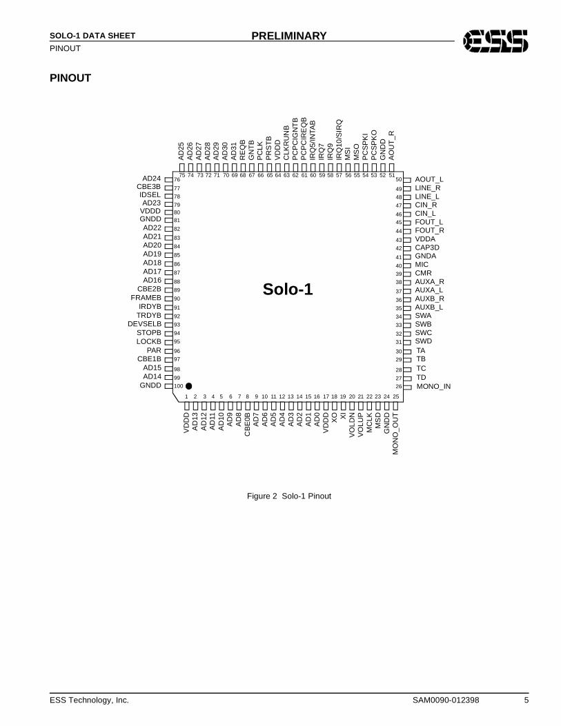
Figure 2 Solo-1 Pinout
1
AOUT_LLINE_RLINE_LCIN_RCIN_LFOUT_LFOUT_RVDDACAP3DGNDAMICCMRAUXA_RAUXA_LAUXB_RAUXB_LSWASWBSWCSWD
GNDDAD22AD21AD20AD19AD18AD17AD16
CBE2BFRAMEB
IRDYBTRDYB
DEVSELBSTOPBLOCKB
PARCBE1B
AD15AD14
GNDD
PC
PC
IRE
QB
PC
PC
IGN
TB
CLK
RU
NB
VD
DD
PR
ST
BP
CLK
GN
TB
RE
QB
AD
31A
D30
AD
29A
D28
AD
27A
D26
AD
25AD24
CBE3BIDSELAD23
VDDD
AO
UT
_RG
ND
DP
CS
PK
OP
CS
PK
IM
SO
MS
IIR
Q10
/SIR
QIR
Q9
IRQ
7IR
Q5/
INTA
B
Solo-1
26
25
50
VO
LDNXI
XO
VD
DD
AD
0A
D1
AD
2A
D3
AD
4A
D5
AD
6A
D7
CB
E0B
AD
8A
D9
AD
10A
D11
AD
12A
D13
VD
DD
TATBTCTDMONO_IN
MO
NO
_OU
TG
ND
DM
SD
MC
LKV
OLU
P
2 3 4 5 6 7 8 9 10 11 12 13 14 15 16 17 18 19 20 21 22 23 24
75 5174 73 72 71 70 69 68 67 66 65 64 63 62 61 60 59 58 57 56 55 54 53 52
49
48
47
4645
44
43
42
41
40
39
38
37
36
35
34
33
32
31
30
29
28
27100
76
77
78
798081
82
83
84
85
86
87
88
89
90
91
92
93
94
95
96
97
98
99

6 SAM0090-012398 ESS Technology, Inc.
SOLO-1 DATA SHEET
PIN DESCRIPTIONPRELIMINARY
PIN DESCRIPTION
Name Number I/O Description
VDDD 1,17,64,80 I Digital supply voltage, 5 V.
AD[31:0] 69:76,79,82:88,98:99,2:7,9:16
I/O Address and data lines from the PCI bus.
CBE[3:0]B 77,89,97,8 I/O PCI command/byte enable.
XO 18 O Oscillator output. Connect to external 14.318 MHz crystal.
XI 19 I Oscillator/external clock input. Connect to external 14.318 MHz crystal or clock source (must be CMOS levels).
VOLDN 20 I Active-low volume decrease button input with internal pull-up.
VOLUP 21 I Active-low volume increase button input with internal pull-up.
MCLK 22 I Input with internal pull-down. Music serial clock from external wavetable music synthesizer (ES689/ES69x).
MSD 23 I Input with internal pull-down. Music serial data from external wavetable music synthesizer (ES689/ES69x).
GNDD 24,52,81,100 I Digital ground.
MONO_OUT 25 O Mono output with source select and volume control (including mute). This pin can drive an external 5k AC load.
MONO_IN 26 I Mono input to mixer and ADC. This pin has an internal pull-up to CMR.
T(A-D) 30:27 I/O Joystick timer pins. These pins connect to the X-Y positioning variable resistors for the two joysticks.
SW(A-D) 34:31 I Active-low joystick switch setting inputs. These SW pins have an internal pull-up resistor.
AUXB_L 35 I Auxiliary B input left. AUXB_L has an internal pull-up resistor to CMR.
AUXB_R 36 I Auxiliary B input right. AUXB_R has an internal pull-up resistor to CMR.
AUXA_L 37 I Auxiliary A input left. AUXA_L has an internal pull-up resistor to CMR. Normally intended for connection to an internal or external CD-ROM analog output.
AUXA_R 38 I Auxiliary A input right. AUXA_R has an internal pull-up resistor to CMR. Normally intended for connection to an internal or external CD-ROM analog output.
CMR 39 O Common mode reference voltage (2.25 V ± 5%). Bypass this pin to analog ground with 47 µF electrolytic in parallel with a .1 µF capacitor.
MIC 40 I Microphone input. MIC has an internal pull-up resistor to CMR.
GNDA 41 I Analog ground.
CAP3D 42 I Bypass capacitor to analog ground for 3-D effects.
VDDA 43 I Analog supply voltage (5 V ± 5%). Must be greater than or equal to VDDD-0.3 V.
FOUT_R 44 O Filter output right. AC-coupled externally to CIN_R to remove DC offsets.
FOUT_L 45 O Filter output left. AC-coupled externally to CIN_L to remove DC offsets.
CIN_L 46 I ADC and first channel DAC mixer input. This pin has an internal 50k pull-up resistor to CMR.
CIN_R 47 I ADC and first channel DAC mixer input. This pin has an internal 50k pull-up resistor to CMR.
LINE_L 48 I Line input left. LINE_L has an internal pull-up resistor to CMR.
LINE_R 49 I Line input right. LINE_R has an internal pull-up resistor to CMR.
AOUT_L 50 O Line-level stereo output left. This pin can drive a 5k ohm AC load.
AOUT_R 51 O Line-level stereo output right. This pin can drive a 5k ohm AC load.

ESS Technology, Inc. SAM0090-012398 7
SOLO-1 DATA SHEET
PIN DESCRIPTIONPRELIMINARY
PCSPKO 53 O Analog output of PCSPKI with volume control.
PCSPKI 54 I Normally low digital PC speaker signal input. This signal is converted to an analog signal with volume control and appears on analog output PCSPKO.
MSO 55 O MIDI serial data output.
MSI 56 I MIDI serial input. Schmitt trigger input with internal pull-up resistor. Either MPU-401 or Sound Blaster formats.
IRQ10 57 O Active-high ISA interrupt request.
SIRQ I/O Serialized IRQ.
IRQ[7,9] 59,58 O Active-high ISA interrupt requests.
IRQ5 60 O Active-high ISA interrupt request.
INTAB O PCI interrupt request.
PCPCIREQB 61 O PC/PCI serialized DREQ output. (Motherboard implementation.)
PCPCIGNTB 62 I PC/PCI serialized DACK input. (Motherboard implementation.)
CLKRUNB 63 I/O PCI clock state for power management.
PRSTB 65 I PCI reset.
PCLK 66 I PCI clock. This clock times all PCI transactions.
GNTB 67 I PCI busmaster grant.
REQB 68 O PCI busmaster request, tristate output.
IDSEL 78 I PCI device select for configuration.
FRAMEB 90 I/O PCI cycle frame.
IRDYB 91 I/O PCI initiator ready.
TRDYB 92 I/O PCI target ready.
DEVSELB 93 I/O PCI device select.
STOPB 94 I/O PCI stop transaction.
LOCKB 95 I/O PCI lock.
PAR 96 I/O PCI parity.
Name Number I/O Description
8 SAM0090-012398 ESS Technology, Inc.
SOLO-1 DATA SHEET
FUNCTIONAL DESCRIPTIONPRELIMINARY
FUNCTIONAL DESCRIPTION
This section shows the overall structure of the Solo-1 anddiscusses its major functional subunits.
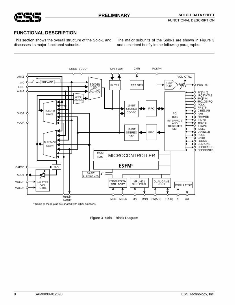
The major subunits of the Solo-1 are shown in Figure 3and described briefly in the following paragraphs.
Figure 3 Solo-1 Block Diagram
AOUT
LINE
VDDA
GNDA
MIC
CMR
AUXA
SW(A-D)
CBE[3:0]B
MSD MCLK
FRAMEB
AD[31:0]
T(A-D)
IRQ10/SIRQPCLK
PAR
PRSTB
XI XO
REF GEN
PCI
DUAL GAME
IRQ[7,9]
VOLUP
VOLDN
BUSINTERFACE
IRQ5/INTAB
RECORD
OSCILLATOR
ES689/ES69xPORTSER. PORT
VDDDGNDD
* Some of these pins are shared with other functions.
ROM
RAM
CODEC
FIFO
IRDYB
MICROCONTROLLER
MSOMSI
MPU-401SER. PORT
STEREO
ESFM™
1-BITDAC PCSPKO
PCSPKICIN FOUT
FILTER
16-BIT
VOL. CTRL.
MIXER
ANDREGISTER
SET
MASTERVOL
CTRL
16-BITSTEREO DAC
FIFO
TRDYB
RECORDSOURCE
MIXER
PLAYBACK
DACSTEREO16-BIT
ANDVOLUME
CONTROL
PREAMP
MIXERSOURCE
CAP3D 3-D
MONOIN/OUT
AUXB
IDSELSTOPB
DEVSELBREQBGNTBLOCKBCLKRUNBPCPCIREQBPCPCIGNTB
ESS Technology, Inc. SAM0090-012398 9
SOLO-1 DATA SHEET
FUNCTIONAL DESCRIPTIONPRELIMINARY
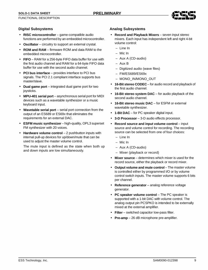
Digital Subsystems
• RISC microcontroller – game-compatible audio functions are performed by an embedded microcontroller.
• Oscillator – circuitry to support an external crystal.
• ROM and RAM – firmware ROM and data RAM to the embedded microcontroller.
• FIFO – RAM for a 256-byte FIFO data buffer for use with the first audio channel and RAM for a 64-byte FIFO data buffer for use with the second audio channel.
• PCI bus interface – provides interface to PCI bus signals. The PCI 2.1 compliant interface supports bus master/slave.
• Dual game port – integrated dual game port for two joysticks.
• MPU-401 serial port – asynchronous serial port for MIDI devices such as a wavetable synthesizer or a music keyboard input.
• Wavetable serial port – serial port connection from the output of an ES689 or ES69x that eliminates the requirements for an external DAC.
• ESFM music s ynthesizer – high-quality, OPL3 superset FM synthesizer with 20 voices.
• Hardware volume control – 2 pushbutton inputs with internal pull-up devices for up/down/mute that can be used to adjust the master volume control.
The mute input is defined as the state when both upand down inputs are low simultaneously.
Analog Subsystems
• Record and Pla yback Mixers – seven input stereo mixers. Each input has independent left and right 4-bit volume control:
– Line In
– Mic In
– Aux A (CD-audio)
– Aux B
– Digitized audio (wave files)
– FM/ES689/ES69x
– MONO_IN/MONO_OUT
• 16-Bit stereo CODEC – for audio record and playback of the first audio channel.
• 16-Bit stereo s ystem DAC – for audio playback of the second audio channel.
• 16-Bit stereo music DAC – for ESFM or external wavetable synthesizer.
• 1-Bit DAC – for PC speaker digital input.
• 3-D Processor – 3-D audio effects processor.
• Record source and input volume control – input source and volume control for recording. The recording source can be selected from one of four choices:
– Line In
– Mic In
– Aux A (CD-audio)
– Mixer (playback or record)
• Mixer source – determines which mixer is used for the record source, either the playback or record mixer.
• Output volume and mute control – The master volume is controlled either by programmed I/O or by volume control switch inputs. The master volume supports 6 bits per channel.
• Reference generator – analog reference voltage generator.
• PC speaker volume control – The PC speaker is supported with a 1-bit DAC with volume control. The analog output pin PCSPKO is intended to be externally mixed at the external amplifier.
• Filter – switched capacitor low-pass filter.
• Pre-amp – 26 dB microphone pre-amplifier.
10 SAM0090-012398 ESS Technology, Inc.
SOLO-1 DATA SHEET
MIXER SCHEMATIC BLOCK DIAGRAMPRELIMINARY
MIXER SCHEMATIC BLOCK DIAGRAM
Figure 4 Solo-1 Mixer Schematic Block Diagram
DMA 1ADC/DAC
digital audio
DAC
DMA 2digital audio
LINE
Mono_In
AUXA
AUXB
AOUT
ADC
Preamp
OutputVolume
Input
PlaybackMixer
Record
Record
Off
On
Record
MasterVolume
Volume
Source
Mixer
Monitor
MIC
DAC
FM
HWWT X
ESS Technology, Inc. SAM0090-012398 11
SOLO-1 DATA SHEET
BUS INTERFACINGPRELIMINARY
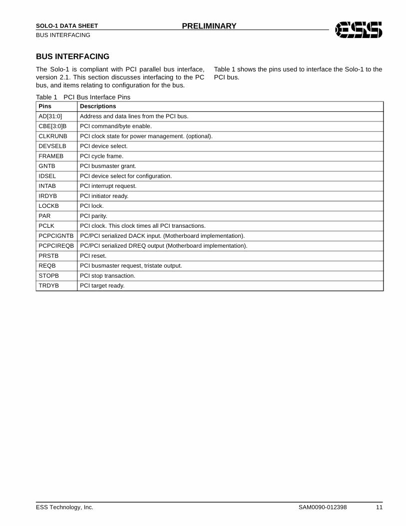
BUS INTERFACING
The Solo-1 is compliant with PCI parallel bus interface,version 2.1. This section discusses interfacing to the PCbus, and items relating to configuration for the bus.
Table 1 shows the pins used to interface the Solo-1 to thePCI bus.
Table 1 PCI Bus Interface PinsPins Descriptions
AD[31:0] Address and data lines from the PCI bus.
CBE[3:0]B PCI command/byte enable.
CLKRUNB PCI clock state for power management. (optional).
DEVSELB PCI device select.
FRAMEB PCI cycle frame.
GNTB PCI busmaster grant.
IDSEL PCI device select for configuration.
INTAB PCI interrupt request.
IRDYB PCI initiator ready.
LOCKB PCI lock.
PAR PCI parity.
PCLK PCI clock. This clock times all PCI transactions.
PCPCIGNTB PC/PCI serialized DACK input. (Motherboard implementation).
PCPCIREQB PC/PCI serialized DREQ output (Motherboard implementation).
PRSTB PCI reset.
REQB PCI busmaster request, tristate output.
STOPB PCI stop transaction.
TRDYB PCI target ready.

12 SAM0090-012398 ESS Technology, Inc.
SOLO-1 DATA SHEET
DIGITAL AUDIOPRELIMINARY
DIGITAL AUDIO
The Solo-1 incorporates two digital audio channels.
Audio 1 The first audio channel. This channel is used for Sound Blaster Pro compatible DMA, Extended mode DMA, and programmed I/O. It can be used for either record or playback.
In DOS mode, this channel uses TDMA, DDMA,or PCPCI to emulate ISA DMA on the PCI bus.Since most DOS games default to DMA channel1, the first audio channel should ideally beassigned to ISA channel 1. However, it ispossible to map audio 1 to one of three DMAchannels (0,1,3) through the PCI configurationregisters.
In Windows mode, this channel can use PCI BusMaster DMA.
Audio 2 The second audio channel. This channel is used for audio playback in full-duplex mode. Audio 2 uses PCI Bus Mastering with burst transfers to minimize PCI bus access.
Figure 5 Data Transfer Modes
Data Formats
See “Data Formats” on page 36.
Audio 1 DMA Transfers in SB Compatibilit y ModeThe first audio channel is programmed using standardSound Blaster compatible commands. These commandsare written to the chip through port SBBase+Ch.
When programming the first audio channel for transfers,one of the following modes can be used:
• Direct mode
• DMA modes
– Normal
– Auto-Initialize
In addition, both DMA Normal mode and DMA Auto-Initialize mode can use a special High-Speed mode.
Direct Mode
In Direct mode, timing for DMA transfers is handled by theapplication program. For example, the system timer canbe reprogrammed to generate interrupts at the desiredsample rate. At each system timer interrupt, the command10h, 11h, 20h, or 21h is issued followed by the sample.Polling of the Write-Buffer-Available flag (SBBase+Ch [bit7]) is required before writing the command and betweenwriting the command and the data.
NOTE: The switched capacitor filter is initialized by resetfor an intended sample rate of 8 kHz. In Direct mode, theapplication may wish to adjust this filter appropriate to theactual sample rate. Do this by programming the timer withcommand 40h just as if the application were using DMAmode.
DMA Modes
In DMA mode, the programmable timer in the Solo-1controls the rate at which samples are sent to the CODEC.The timer is programmed using command 40h, which alsosets up the programmable filters inside the Solo-1. TheSolo-1 firmware maintains an internal FIFO (32 levels for16-bit transfers, 64 levels for 8-bit transfers) that is filled byDMA transfers and emptied by timed transfers to the DAC.
Before a DMA transfer, the application first programs theDMA controller for the desired transfer size and address,then programs the Solo-1 with the same size information.At the end of the transfer, the Solo-1 generates aninterrupt request, indicating that the current block transferis complete. The FIFO gives the application programsufficient time to respond to the interrupt and initiate thenext block transfer.
The Solo-1 supports both Normal DMA mode and Auto-Initialize DMA mode.
Normal DMA ModeIn Normal mode DMA transfers, the DMA controller mustbe initialized and the Solo-1 commanded for every blockthat is transferred.
Auto-Initialize DMA ModeIn Auto-Initialize mode, the DMA transfer is continuous, ina circular buffer, and the Solo-1 generates an interrupt forthe transition between buffer halves. In this mode the DMAcontroller and Solo-1 only need to be set up once.
Digital Audio
Audio 1 Audio 2
CompatibilityMode
ExtendedMode
DirectMode
DMAMode
ProgrammedDMAMode I/O
PCIBusmaster
Native PCIMode
DMA
ESS Technology, Inc. SAM0090-012398 13
SOLO-1 DATA SHEET
DIGITAL AUDIOPRELIMINARY
High-Speed ModeThe Solo-1 supports mono 8-bit DMA transfers at a rate upto 44 kHz. Mono 16-bit transfers are supported up to a rateof 22 kHz.
The special “High-Speed mode” allows 8-bit sampling upto 44 kHz for ADC, using commands 98h (auto-initialize)and 99h (normal). No automatic gain control (AGC) isperformed. The input volume is controlled with commandDDh.
Audio 1 DMA Transfers in Extended ModeThe first audio channel is programmed using the controllerregisters internal to the Solo-1. The commands written tothe controller registers are written to the chip through portSBBase+Ch.
When programming the first audio channel for transfers,one of the following modes can be used:
• Programmed I/O
• DMA modes
– Normal (Single or Demand transfer)
– Auto-Initialize (Single or Demand transfer)
In addition, both DMA normal mode and DMA auto-initialize mode use Single transfer or Demand transfermodes.
Programmed I/O
For some applications, DMA mode is not suitable oravailable for data transfer, and it is not possible to takeexclusive control of the system for DAC and ADCtransfers. In these situations, use I/O block transfers withinan interrupt handler. The REP OUTSB instruction of the80x86 family transfers data from memory to an I/O portspecified by the DX register. The REP INSB instruction isthe complementary function. Use Solo-1 port SBBase+Fhfor block transfers.
I/O transfers to FIFO are nearly identical to the DMAprocess, except that an I/O access to port SBBase+Fhreplaces the DMA cycle. For details about programmedI/O operation see “Extended Mode Programmed I/OOperation” on page 43.
DMA Modes
Extended mode DMA supports both Normal and Auto-Ini-tialize mode. In addition Normal mode and Auto-Initialize mode both support Single and Demand transfer modes.
Single TransferOne byte is transferred per DMA request.
Demand Transfer
To reduce the number of DMA requests necessary tomake a transfer, two or four bytes are transferred per DMArequest (DRQ). Using Demand transfer enables multipleDMA acknowledges for each DMA request.
For a description of DMA mode including Normal DMAmode and Auto-Initialize DMA mode see “DMA Modes” onpage 12.
Extended Mode Audio 1 Controller Registers
The following registers control operation of the first audiochannel in Extended mode:
Audio 1 DMA Transfers in Native PCI ModeUnlike DOS game environments, the Solo-1 can becompletely controlled by drivers. This way the Solo-1 canperform Bus Master DMA for first channel audio datatransfers under Windows (or other operating systems).
Data Transfers Usin g the Second Audio ChannelThe second audio channel is programmed using mixerregisters 70h through 7Ch. The commands written to themixer registers are written to the chip through portsSBBase+4h and SBBase+5h.
The second audio channel always uses PCI Bus Mastertransfers instead of ISA-like DMA. IOBase+0h –IOBase+6h control Audio 2 Bus Master DMA. Both normaland auto-initialize modes are available, as in ISA-DMA.DMA counts for Audio 2 must be in multiples of 16 bytes,so that the Solo-1 can performs 4 DWord burst transfers.
Table 2 Extended Mode Audio 1 Controller Registers
Address Name
A1h Audio 1 Sample Rate Generator register
A2h Audio 1 Filter Clock Divider register
A4h Audio 1 Transfer Count Reload register – low byte
A5h Audio 1 Transfer Count Reload register – high byte
B1h Legacy Audio Interrupt Control register
B2h Audio 1 DRQ Control register
B4h Input Volume Control register
B5h Audio 1 DAC Direct Access register – low byte
B6h Audio 1 DAC Direct Access register – high byte
B7h Audio 1 Control 1 register
B8h Audio 1 Control 2 register
B9h Audio 1 Transfer Type register
14 SAM0090-012398 ESS Technology, Inc.
SOLO-1 DATA SHEET
DIGITAL AUDIOPRELIMINARY
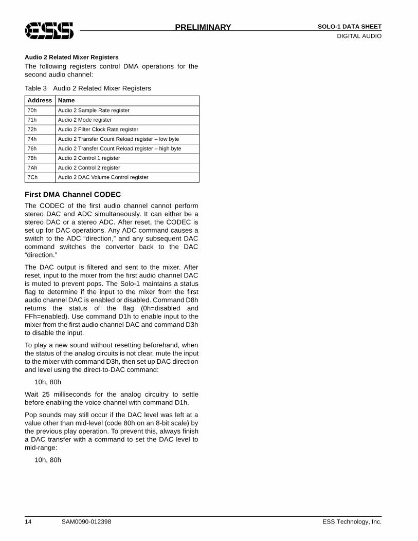
Audio 2 Related Mixer Registers
The following registers control DMA operations for thesecond audio channel:
First DMA Channel CODEC
The CODEC of the first audio channel cannot performstereo DAC and ADC simultaneously. It can either be astereo DAC or a stereo ADC. After reset, the CODEC isset up for DAC operations. Any ADC command causes aswitch to the ADC “direction,” and any subsequent DACcommand switches the converter back to the DAC“direction.”
The DAC output is filtered and sent to the mixer. Afterreset, input to the mixer from the first audio channel DACis muted to prevent pops. The Solo-1 maintains a statusflag to determine if the input to the mixer from the firstaudio channel DAC is enabled or disabled. Command D8hreturns the status of the flag (0h=disabled andFFh=enabled). Use command D1h to enable input to themixer from the first audio channel DAC and command D3hto disable the input.
To play a new sound without resetting beforehand, whenthe status of the analog circuits is not clear, mute the inputto the mixer with command D3h, then set up DAC directionand level using the direct-to-DAC command:
10h, 80h
Wait 25 milliseconds for the analog circuitry to settlebefore enabling the voice channel with command D1h.
Pop sounds may still occur if the DAC level was left at avalue other than mid-level (code 80h on an 8-bit scale) bythe previous play operation. To prevent this, always finisha DAC transfer with a command to set the DAC level tomid-range:
10h, 80h
Table 3 Audio 2 Related Mixer Registers
Address Name
70h Audio 2 Sample Rate register
71h Audio 2 Mode register
72h Audio 2 Filter Clock Rate register
74h Audio 2 Transfer Count Reload register – low byte
76h Audio 2 Transfer Count Reload register – high byte
78h Audio 2 Control 1 register
7Ah Audio 2 Control 2 register
7Ch Audio 2 DAC Volume Control register
ESS Technology, Inc. SAM0090-012398 15
SOLO-1 DATA SHEET
INTERRUPTSPRELIMINARY
INTERRUPTS
There are four interrupt sources in the Solo-1, shown in Table 4.
Interrupt Status Register
Port IOBase+7h of the configuration device can be read toquickly find out which Solo-1 interrupt sources are active.The bits are:
Interrupt Mask Register
Port IOBase+7h can be used to mask any of the fourinterrupt sources, with the exception of the Audio 1interrupt. The Audio 1 interrupt request can be enabled bybit 4 of IOBase+7h, or when bit 15 of PCI Configurationregister 40h (Legacy Audio Control register) is 0.
The mask bits can be used to force the interrupt source tobe zero, without putting the interrupt pin in a high-impedance state. Each bit is AND'ed with thecorresponding interrupt source. This register is set to allzeros by hardware reset.
The Interrupt Status register (ISR) is not affected by thestate of the Interrupt Mask register (IMR). That is, the ISRreflects the status of the interrupt request lines beforebeing masked by the IMR.
The IMR is useful because the Solo-1 shares interrupts.For example, assume that Audio 1, Audio 2, HardwareVolume, and MPU-401 all share the same interrupt inWindows. When returning from Windows to DOS, theHardware Volume, MPU-401, and Audio 2 interrupts canbe masked by setting the appropriate bits to 0.
A second use is within an interrupt handler. The first thingthe interrupt handler can do is mask all the interruptsources mapped to the interrupt handler. Then, the ISRcan be polled to decide which sources to process. Justbefore exiting the interrupt handler, the IMR can berestored. If an unprocessed interrupt remains active, itgenerates an interrupt request because the interrupt pinwas deasserted during the masked period and then wasasserted when the interrupt sources were unmasked.Also, while the interrupts are masked, the individualinterrupt sources can change state any number of timeswithout generating a false interrupt request.
Table 4 Solo-1 Interrupt Sources
Interrupt Source Description
Audio 1 An interrupt used for the first DMA channel (Sound Blaster compatible DMA, Extended mode DMA, and Extended mode programmed I/O), as well as Sound Blaster-compatible MIDI receive. Controller register B1h controls use of this interrupt for Extended mode DMA and programmed I/O. This interrupt request is cleared by hardware or software reset, or an I/O read from port SBBase+0Eh. The interrupt request can be polled by reading from port SBBase+0Ch.
Audio 2 An optional interrupt for the second DMA channel. The Solo-1 can operate in full-duplex mode using two DMA channels. However, since the second DMA channel must share the same sample rate as the first DMA chan-nel, it is not necessary to use a separate interrupt for the second DMA channel. The Audio 2 interrupt is masked by bit 6 of mixer register 7Ah. It can be polled and cleared by reading or writing bit 7 of register 7Ah.
Hardware Volume Hardware volume activity interrupt. This interrupt occurs when one of the three hardware volume controls changes state. Bit 1 of mixer register 64h is the mask bit for this interrupt. The interrupt request can be polled by reading bit 3 of register 64h. The interrupt request is cleared by writing any value to register 66h. Typically this interrupt, if used, is shared with an audio interrupt.
MPU-401 The MPU-401 interrupt occurs when a MIDI byte is received. It goes low when a byte is read from the MIDI FIFO and goes high again quickly if there are additional bytes in the FIFO. The interrupt status is the same as the Read-Data-Available status flag in the MPU-401 status register. The MPU-401 interrupt is masked by bit 6 of mixer register 64h.
Table 5 Interrupt Status Bits in IOBase+7h
Bit Description
4 Audio 1 interrupt request
5 Audio 2 interrupt request AND'ed with bit 6 of mixer register 7Ah
6 Hardware volume interrupt request AND'ed with bit 1 of mixer register 64h
7 MPU-401 receive interrupt request AND'ed with bit 6 of mixer register 64h
16 SAM0090-012398 ESS Technology, Inc.
SOLO-1 DATA SHEET
PERIPHERAL INTERFACINGPRELIMINARY
PERIPHERAL INTERFACING
Wavetable Interface
The Solo-1 contains a synchronous serial interface forconnection to an ES689/ES69x wavetable musicsynthesizer. Table 6 identifies pins in the wavetable interface.
Joystick / MPU-401 Interface
MPU-401 UART ModeThere is one MIDI interface in the Solo-1, an MPU-401“UART mode” compatible serial port. MPU-401 is asuperior method of MIDI serial I/O because it does notinterfere with DAC or ADC Sound Blaster commands.
MPU-401 requires an interrupt channel for MIDI receive.This interrupt should be selected using mixer register 64h.It should be different than the interrupt selected for audioDMA interrupts.
Joystick / MIDI External InterfaceThe joystick portion of the Solo-1 reference design isidentical to that on a standard PC game control adaptor orgame port. The PC compatible joystick can be connectedto a 15-pin D-sub connector. It supports all standard PCjoystick-compatible software. If the system already has agame card or port, remove the game card.
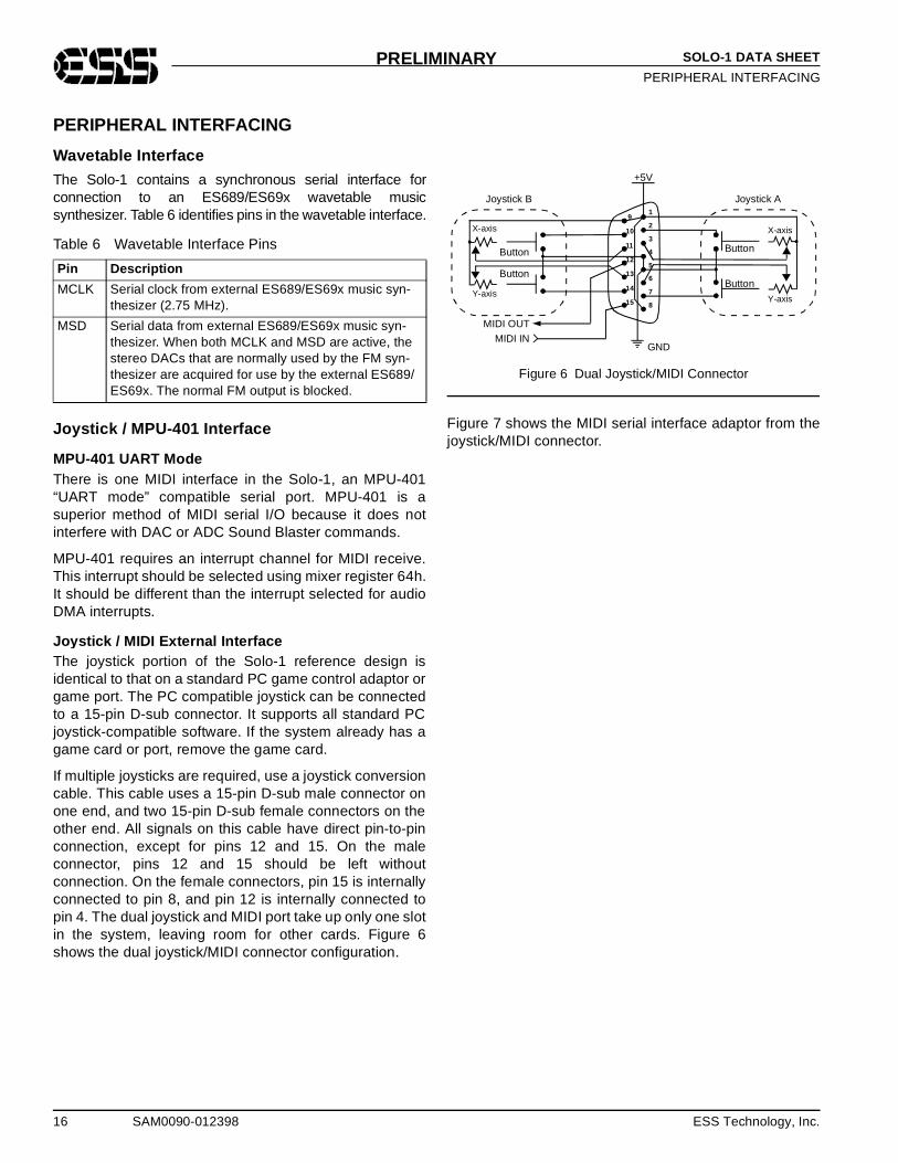
If multiple joysticks are required, use a joystick conversioncable. This cable uses a 15-pin D-sub male connector onone end, and two 15-pin D-sub female connectors on theother end. All signals on this cable have direct pin-to-pinconnection, except for pins 12 and 15. On the maleconnector, pins 12 and 15 should be left withoutconnection. On the female connectors, pin 15 is internallyconnected to pin 8, and pin 12 is internally connected topin 4. The dual joystick and MIDI port take up only one slotin the system, leaving room for other cards. Figure 6shows the dual joystick/MIDI connector configuration.
Figure 6 Dual Joystick/MIDI Connector
Figure 7 shows the MIDI serial interface adaptor from thejoystick/MIDI connector.
Table 6 Wavetable Interface Pins
Pin Description
MCLK Serial clock from external ES689/ES69x music syn-thesizer (2.75 MHz).
MSD Serial data from external ES689/ES69x music syn-thesizer. When both MCLK and MSD are active, the stereo DACs that are normally used by the FM syn-thesizer are acquired for use by the external ES689/ES69x. The normal FM output is blocked.
+5V
Button
Button
MIDI OUT
MIDI INGND
Button
Button
Joystick B Joystick A
X-axis
Y-axis
X-axis
Y-axis
1
2
3
4
5
6
7
8
9
10
11
12
13
14
15
ESS Technology, Inc. SAM0090-012398 17
SOLO-1 DATA SHEET
PERIPHERAL INTERFACINGPRELIMINARY
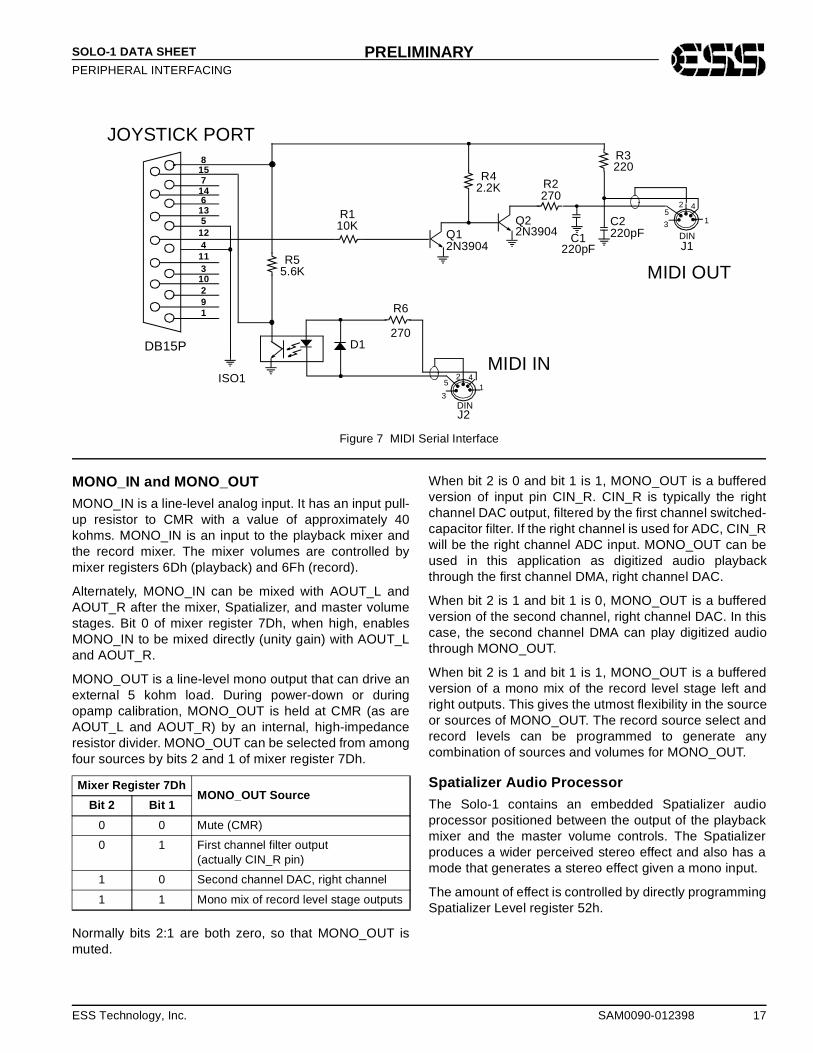
Figure 7 MIDI Serial Interface
MONO_IN and MONO_OUT
MONO_IN is a line-level analog input. It has an input pull-up resistor to CMR with a value of approximately 40kohms. MONO_IN is an input to the playback mixer andthe record mixer. The mixer volumes are controlled bymixer registers 6Dh (playback) and 6Fh (record).
Alternately, MONO_IN can be mixed with AOUT_L andAOUT_R after the mixer, Spatializer, and master volumestages. Bit 0 of mixer register 7Dh, when high, enablesMONO_IN to be mixed directly (unity gain) with AOUT_Land AOUT_R.
MONO_OUT is a line-level mono output that can drive anexternal 5 kohm load. During power-down or duringopamp calibration, MONO_OUT is held at CMR (as areAOUT_L and AOUT_R) by an internal, high-impedanceresistor divider. MONO_OUT can be selected from amongfour sources by bits 2 and 1 of mixer register 7Dh.
Normally bits 2:1 are both zero, so that MONO_OUT ismuted.
When bit 2 is 0 and bit 1 is 1, MONO_OUT is a bufferedversion of input pin CIN_R. CIN_R is typically the rightchannel DAC output, filtered by the first channel switched-capacitor filter. If the right channel is used for ADC, CIN_Rwill be the right channel ADC input. MONO_OUT can beused in this application as digitized audio playbackthrough the first channel DMA, right channel DAC.
When bit 2 is 1 and bit 1 is 0, MONO_OUT is a bufferedversion of the second channel, right channel DAC. In thiscase, the second channel DMA can play digitized audiothrough MONO_OUT.
When bit 2 is 1 and bit 1 is 1, MONO_OUT is a bufferedversion of a mono mix of the record level stage left andright outputs. This gives the utmost flexibility in the sourceor sources of MONO_OUT. The record source select andrecord levels can be programmed to generate anycombination of sources and volumes for MONO_OUT.
Spatializer Audio Processor
The Solo-1 contains an embedded Spatializer audioprocessor positioned between the output of the playbackmixer and the master volume controls. The Spatializerproduces a wider perceived stereo effect and also has amode that generates a stereo effect given a mono input.
The amount of effect is controlled by directly programmingSpatializer Level register 52h.
1
2
3
4
5
6
7
8
9
10
11
12
13
14
15
1
1
2
2
3
4
3
4
5
5
JOYSTICK PORT
DB15P
ISO1
R55.6K
R110K
R42.2K R2
270
R3220
C1220pF
C2220pF
Q22N3904Q1
2N3904
R6
270D1
DIN
DINJ1
J2
MIDI IN
MIDI OUT
Mixer Register 7DhMONO_OUT Source
Bit 2 Bit 1
0 0 Mute (CMR)
0 1 First channel filter output(actually CIN_R pin)
1 0 Second channel DAC, right channel
1 1 Mono mix of record level stage outputs

18 SAM0090-012398 ESS Technology, Inc.
SOLO-1 DATA SHEET
PERIPHERAL INTERFACINGPRELIMINARY
Hardware and Master Volume Control
Two external pins, VOLUP and VOLDN, can be connectedto external momentary switches to ground to implementhardware master volume controls. Pressing one of thesebuttons produces a low signal to one of the inputs andthereby changes the master volume.
MUTE is emulated by the state where both VOLUP andVOLDN inputs are low simultaneously.
The up and down buttons produce a single step change involume when they are first pressed. If these buttons areheld down, they enter a fast-scrolling mode. The singlestep change can be either one volume unit (.75 dB) orthree volume units (2.25 dB). In scrolling mode, the stepchange is always one volume unit.
The two inputs have debounce circuitry within the Solo-1.Hold each input low for 40 milliseconds or more for it to berecognized as a valid button press. Hold each input highfor 40 milliseconds or more between button presses. Asoftware option allows the debounce time to be reducedfrom 40 milliseconds to 10 microseconds.
Normally the hardware volume controls directly changethe master volume registers and produce an interrupt ateach change. However, the Solo-1 can be programmed sothat the hardware volume controls do not directly changethe master volume registers. This is called “split mode”, inwhich the hardware volume control counters are split fromthe master volume registers. Pressing a hardware volumecontrol button changes the hardware volume counters andproduces an interrupt. The host software can read thehardware volume counters and update the master volumeregisters as needed. Split mode is enabled by bit 7 ofmixer register 64h.
For support of mixer master volume control, a write tomixer registers 22h or 32h translates automatically intowrites to the master volume registers. Since register 22honly has 3-bit resolution per channel, and register 32h onlyhas 4-bit resolution per channel, a translation circuit isincluded in the Solo-1 that translates 3- or 4-bit volumevalues into the 6-bit volume + mute that is used in themaster volume registers. Support of these mixer registerscan be defeated under software control.
Reading master volume registers 22h or 32h also requiresa translation circuit to translate 6-bit + mute mastervolumes into 3- or 4-bit master volume numbers forregisters 22h or 32h.
PC Speaker
The PC Speaker is supported with a 1-bit DAC withvolume control. The analog output pin PCSPKO isintended to be externally mixed at the external amplifier.
PC Speaker Volume ControlWhen the PCSPKI signal is high, a resistive path to analogpower is enabled. The value of the resistor is selectedfrom among 7 choices to control the amplitude of theoutput signal.
Figure 8 PC Speaker Volume Circuitry
With the external circuit shown in Figure 8, the amplitudeof a square wave output on pin PCSPKO should beapproximately VDDD/2 for maximum volume, i.e., theinternal resistor is approximately 500 ohms (± 30%). Theother levels are relative to this amplitude as follows:
off, -18dB, -15dB, -12dB, -9dB, -6dB, -3dB, +0dB
The purpose of the circuit, beyond volume control of thespeaker, is to prevent digital noise from the PC speakersignal being mixed into the analog signal. This circuitprovides a clean analog signal. The output can be eithermixed with the AOUT_L and AOUT_R pins externally or itcan be used to drive a simple transistor amplifier to drivean 8 ohm speaker dedicated to producing beeps.
PCSPKI
VDDD
PCSPKO
.01 µF
.1 µF
500
GNDA

ESS Technology, Inc. SAM0090-012398 19
SOLO-1 DATA SHEET
ANALOG DESIGN CONSIDERATIONSPRELIMINARY
ANALOG DESIGN CONSIDERATIONS
This section describes design considerations related toinputs and outputs of analog signals and related pins onthe chip.
Game Port
The game port address GPBase+1h is decoded for timerpins TA, TB, TC, and TD, and switch pins SWA, SWB,SWC, and SWD. The MIDI serial input and output alsocome from the game port connector in most applications.
Reference Generator
Reference generator pin CMR is shown bypassed toanalog ground.
Figure 9 Reference Generator Pin Diagram
Switched-Capacitor Filter
The outputs of the FOUT_L and FOUT_R filters must beAC-coupled to the inputs CIN_L and CIN_R. This providesfor DC blocking and an opportunity for low-pass filteringwith capacitors to analog ground at these inputs.
Figure 10 Switched-Capacitor Filter Pin Diagram
Audio Inputs and Outputs
Analog inputs MIC, LINE_L, LINE_R, AUXA_L, andAUXA_R should be capacitively coupled to theirrespective input signals. All have pull-up resistors to CMR.
Solo-1 analog outputs AOUT_L and AOUT_R should beAC-coupled to an amplifier, volume control potentiometer,or line-level outputs.
Solo-1
CMR47 µF
.1 µF
+
Solo-1
FOUT_L
CIN_L
.22 µF
.22 µFFOUT_R
CIN_R680 pF
680 pF
20 SAM0090-012398 ESS Technology, Inc.
SOLO-1 DATA SHEET
PCI CONFIGURATION REGISTERSPRELIMINARY
PCI CONFIGURATION REGISTERS
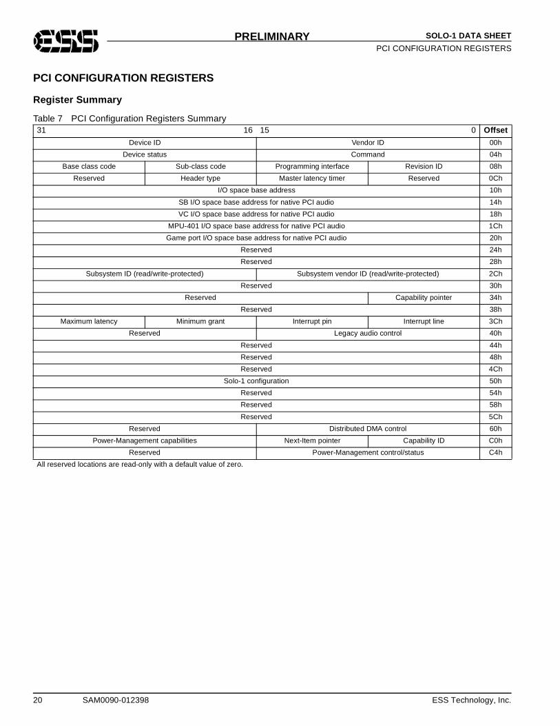
Register Summary
Table 7 PCI Configuration Registers Summary 31 16 15 0 Offset
Device ID Vendor ID 00h
Device status Command 04h
Base class code Sub-class code Programming interface Revision ID 08h
Reserved Header type Master latency timer Reserved 0Ch
I/O space base address 10h
SB I/O space base address for native PCI audio 14h
VC I/O space base address for native PCI audio 18h
MPU-401 I/O space base address for native PCI audio 1Ch
Game port I/O space base address for native PCI audio 20h
Reserved 24h
Reserved 28h
Subsystem ID (read/write-protected) Subsystem vendor ID (read/write-protected) 2Ch
Reserved 30h
Reserved Capability pointer 34h
Reserved 38h
Maximum latency Minimum grant Interrupt pin Interrupt line 3Ch
Reserved Legacy audio control 40h
Reserved 44h
Reserved 48h
Reserved 4Ch
Solo-1 configuration 50h
Reserved 54h
Reserved 58h
Reserved 5Ch
Reserved Distributed DMA control 60h
Power-Management capabilities Next-Item pointer Capability ID C0h
Reserved Power-Management control/status C4h
All reserved locations are read-only with a default value of zero.

ESS Technology, Inc. SAM0090-012398 21
SOLO-1 DATA SHEET
PCI CONFIGURATION REGISTERSPRELIMINARY
Register Descriptions
Vendor ID (00h, 01h, R)
Bit Definitions:
Device ID (02h, 03h, R)
Bit Definitions:
Command (04h, 05h, R/W)
The default value after reset is 0000h.
Bit Definitions:
Device Status (06h, 07h, R/WC)
The default value after reset is 0290h. Writing 1 clears abit; writing 0 has no effect on a bit.
Bit Definitions:
Revision ID (08h, R)
Bit Definitions:
Programmin g Interface (09h, R)
Bit Definitions:
Sub-Class Code (0Ah, R)
Bit Definitions:
Vendor ID
15 14 13 12 11 10 9 8 7 6 5 4 3 2 1 0
Bits Name Description
15:0 Vendor ID The default value after reset is 125Dh, indicat-ing ESS as the manufacturer of this device.
Device ID
15 14 13 12 11 10 9 8 7 6 5 4 3 2 1 0
Bits Name Description
15:0 Device ID The default value after reset is 1969h, identi-fying the Solo-1 as this device.
0 0 0 0 0 0 0 0 0 0 0 0 0 BME 0 IOS
15 14 13 12 11 10 9 8 7 6 5 4 3 2 1 0
Bits Name Description
15:3 – Reserved. Returns 0 when read.
2 BME Bus Master enable.
1 – Reserved. Returns 0 when read.
0 IOS I/O Space access enable.
0 0 MAS RTA STA DT DPE FBC UDF 66M ACPI 0 0 0 0
15 14 13 12 11 10 9 8 7 6 5 4 3 2 1 0
Bits Name Description
15:14 – Reserved. Returns 0 when read.
13 MAS Master abort status (read/write-clear).
12 RTA Received target abort status (read/write-clear).
11 STA Signaled target abort (read-only: 0).
10:9 DT DEVSEL timing (read-only: 01 = medium).
8 DPE Data parity error detected (read-only: 0).
7 FBC Fast back-to-back capable (read-only: 1).
6 UDF UDF supported (read-only: 0).
5 66M 66 MHz capable (read-only: 0).
4 ACPI ACPI capable (read-only: 1).
3:0 – Reserved. Returns 0 when read.
Revision ID
7 6 5 4 3 2 1 0
Bits Name Description
7:0 Revision ID Identifies the revision of this device. The default value after reset is 00h.
Programming interface
7 6 5 4 3 2 1 0
Bits Name Description
7:0 PI Identifies the programming interface of this device. The default value after reset is 00h.
Sub-Class code
7 6 5 4 3 2 1 0
Bits Name Description
7:0 SCC The default value after reset (assigned by the PCI-SIG) is 01h, indicating an audio device with a multimedia base class.

22 SAM0090-012398 ESS Technology, Inc.
SOLO-1 DATA SHEET
PCI CONFIGURATION REGISTERSPRELIMINARY
Base Class Code (0Bh, R)
Bit Definitions:
Master Latenc y Timer (0Dh, R/W)
The default value after reset is 00h.
Bit Definitions:
Header Type (0Eh, R)
Bit Definitions:
I/O Base (10h – 13h, R/W )
The default value after reset is 000xxx1h.
Bit Definitions:
SB Base for Native-PCI-Audio (14h – 17h, R/W )
The default value after reset is 000xxx1h.
Bit Definitions:
VC Base for Native-PCI-Audio (18h – 1Bh, R/W )
The default value after reset is 000xxx1h.
Bit Definitions:
MPU Base for Native-PCI-Audio (1Ch – 1Fh, R/W )
The default value after reset is 000xxx1h.
Bit Definitions:
Base class code
7 6 5 4 3 2 1 0
Bits Name Description
7:0 BCC The default value after reset (assigned by the PCI-SIG) is 04h, indicating a multimedia device.
Master latency timer count value 0 0 0 0
7 6 5 4 3 2 1 0
Bits Name Description
7:4 MLTCV Master latency timer count value.
3:0 – Reserved. Returns 0 when read.
Header type
7 6 5 4 3 2 1 0
Bits Name Description
7:0 HEDT Header type. A value of 00h indicates a single-function PCI device.
0 0 0 0 0 0 0 0 0 0 0 0 0 0 0 0
31 30 29 28 27 26 25 24 23 22 21 20 19 18 17 16
IOSB 0 0 0 ISI
15 14 13 12 11 10 9 8 7 6 5 4 3 2 1 0
Bits Name Description
31:16 – Hardwired to 0000h.
15:4 IOSB I/O space base address. The Solo-1 claims 16 bytes of IO space.
3:1 – Hardwired to 00h.
0 ISI I/O space indicator. Hardwired to 1.
0 0 0 0 0 0 0 0 0 0 0 0 0 0 0 0
31 30 29 28 27 26 25 24 23 22 21 20 19 18 17 16
SBSB 0 0 0 ISI
15 14 13 12 11 10 9 8 7 6 5 4 3 2 1 0
Bits Name Description
31:16 – Hardwired to 000h.
15:4 SBSB SB space base address for native PCI audio. The Solo-1 claims 16 bytes of Sound Blaster IO space.
3:1 – Hardwired to 00h.
0 ISI I/O space indicator. Hardwired to 1.
0 0 0 0 0 0 0 0 0 0 0 0 0 0 0 0
31 30 29 28 27 26 25 24 23 22 21 20 19 18 17 16
VCSB 0 0 0 ISI
15 14 13 12 11 10 9 8 7 6 5 4 3 2 1 0
Bits Name Description
31:16 – Hardwired to 000h.
15:4 VCSB VC space base address for native PCI audio. The Solo-1 claims 16 bytes of driver IO space. The driver can use allocated IO ports for the DDMA base address.
3:1 – Hardwired to 00h.
0 ISI I/O space indicator. Hardwired to 1.
0 0 0 0 0 0 0 0 0 0 0 0 0 0 0 0
31 30 29 28 27 26 25 24 23 22 21 20 19 18 17 16
MPUSB 0 ISI
15 14 13 12 11 10 9 8 7 6 5 4 3 2 1 0
Bits Name Description
31:16 – Hardwired to 000h.
15:2 MPUSB MPU space base address for native PCI audio. The Solo-1 claims 4 bytes of MPU-401 IO space.
1 – Hardwired to 0.
0 ISI I/O space indicator. Hardwired to 1.
ESS Technology, Inc. SAM0090-012398 23
SOLO-1 DATA SHEET
PCI CONFIGURATION REGISTERSPRELIMINARY
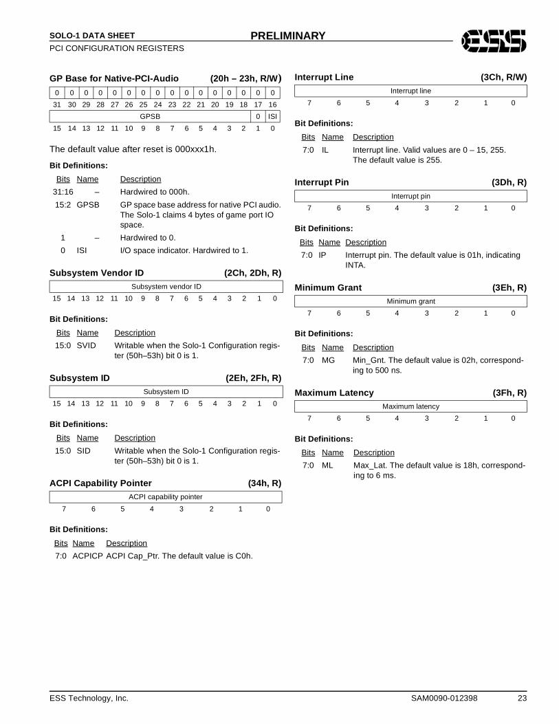
GP Base for Native-PCI-Audio (20h – 23h, R/W )
The default value after reset is 000xxx1h.
Bit Definitions:
Subs ystem Vendor ID (2Ch, 2Dh, R)
Bit Definitions:
Subs ystem ID (2Eh, 2Fh, R)
Bit Definitions:
ACPI Capabilit y Pointer (34h, R)
Bit Definitions:
Interrupt Line (3Ch, R/W)
Bit Definitions:
Interrupt Pin (3Dh, R)
Bit Definitions:
Minimum Grant (3Eh, R)
Bit Definitions:
Maximum Latenc y (3Fh, R)
Bit Definitions:
0 0 0 0 0 0 0 0 0 0 0 0 0 0 0 0
31 30 29 28 27 26 25 24 23 22 21 20 19 18 17 16
GPSB 0 ISI
15 14 13 12 11 10 9 8 7 6 5 4 3 2 1 0
Bits Name Description
31:16 – Hardwired to 000h.
15:2 GPSB GP space base address for native PCI audio. The Solo-1 claims 4 bytes of game port IO space.
1 – Hardwired to 0.
0 ISI I/O space indicator. Hardwired to 1.
Subsystem vendor ID
15 14 13 12 11 10 9 8 7 6 5 4 3 2 1 0
Bits Name Description
15:0 SVID Writable when the Solo-1 Configuration regis-ter (50h–53h) bit 0 is 1.
Subsystem ID
15 14 13 12 11 10 9 8 7 6 5 4 3 2 1 0
Bits Name Description
15:0 SID Writable when the Solo-1 Configuration regis-ter (50h–53h) bit 0 is 1.
ACPI capability pointer
7 6 5 4 3 2 1 0
Bits Name Description
7:0 ACPICP ACPI Cap_Ptr. The default value is C0h.
Interrupt line
7 6 5 4 3 2 1 0
Bits Name Description
7:0 IL Interrupt line. Valid values are 0 – 15, 255.The default value is 255.
Interrupt pin
7 6 5 4 3 2 1 0
Bits Name Description
7:0 IP Interrupt pin. The default value is 01h, indicating INTA.
Minimum grant
7 6 5 4 3 2 1 0
Bits Name Description
7:0 MG Min_Gnt. The default value is 02h, correspond-ing to 500 ns.
Maximum latency
7 6 5 4 3 2 1 0
Bits Name Description
7:0 ML Max_Lat. The default value is 18h, correspond-ing to 6 ms.
24 SAM0090-012398 ESS Technology, Inc.
SOLO-1 DATA SHEET
PCI CONFIGURATION REGISTERSPRELIMINARY
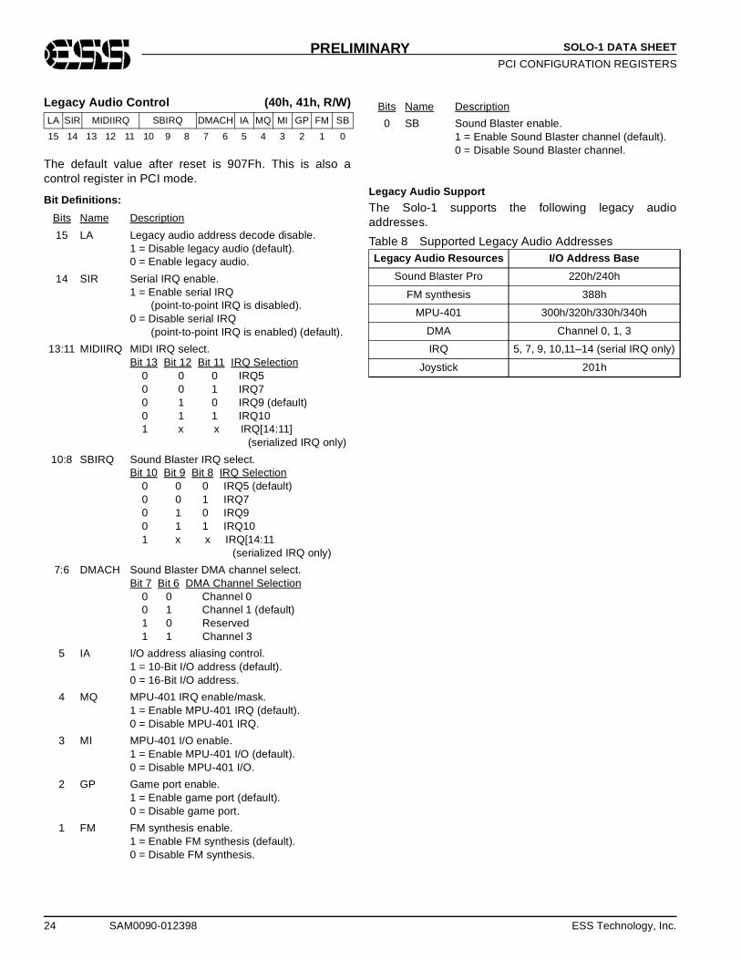
Legacy Audio Control (40h, 41h, R/W)
The default value after reset is 907Fh. This is also acontrol register in PCI mode.
Bit Definitions:Legacy Audio Support
The Solo-1 supports the following legacy audioaddresses.
LA SIR MIDIIRQ SBIRQ DMACH IA MQ MI GP FM SB
15 14 13 12 11 10 9 8 7 6 5 4 3 2 1 0
Bits Name Description
15 LA Legacy audio address decode disable.1 = Disable legacy audio (default).0 = Enable legacy audio.
14 SIR Serial IRQ enable.1 = Enable serial IRQ (point-to-point IRQ is disabled).0 = Disable serial IRQ (point-to-point IRQ is enabled) (default).
13:11 MIDIIRQ MIDI IRQ select.Bit 13 Bit 12 Bit 11 IRQ Selection 0 0 0 IRQ5 0 0 1 IRQ7 0 1 0 IRQ9 (default) 0 1 1 IRQ10 1 x x IRQ[14:11] (serialized IRQ only)
10:8 SBIRQ Sound Blaster IRQ select.Bit 10 Bit 9 Bit 8 IRQ Selection 0 0 0 IRQ5 (default) 0 0 1 IRQ7 0 1 0 IRQ9 0 1 1 IRQ10 1 x x IRQ[14:11 (serialized IRQ only)
7:6 DMACH Sound Blaster DMA channel select.Bit 7 Bit 6 DMA Channel Selection 0 0 Channel 0 0 1 Channel 1 (default) 1 0 Reserved 1 1 Channel 3
5 IA I/O address aliasing control.1 = 10-Bit I/O address (default).0 = 16-Bit I/O address.
4 MQ MPU-401 IRQ enable/mask.1 = Enable MPU-401 IRQ (default).0 = Disable MPU-401 IRQ.
3 MI MPU-401 I/O enable.1 = Enable MPU-401 I/O (default).0 = Disable MPU-401 I/O.
2 GP Game port enable.1 = Enable game port (default).0 = Disable game port.
1 FM FM synthesis enable.1 = Enable FM synthesis (default).0 = Disable FM synthesis.
0 SB Sound Blaster enable.1 = Enable Sound Blaster channel (default).0 = Disable Sound Blaster channel.
Table 8 Supported Legacy Audio AddressesLegacy Audio Resources I/O Address Base
Sound Blaster Pro 220h/240h
FM synthesis 388h
MPU-401 300h/320h/330h/340h
DMA Channel 0, 1, 3
IRQ 5, 7, 9, 10,11–14 (serial IRQ only)
Joystick 201h
Bits Name Description

ESS Technology, Inc. SAM0090-012398 25
SOLO-1 DATA SHEET
PCI CONFIGURATION REGISTERSPRELIMINARY
Solo-1 Confi guration (50h – 53h, R/W)
The default value after reset is 00000000h.
Bit Definitions:
Distributed DMA Control (60h, 61h, R/W)
The default value after reset is 0000h.
Bit Definitions:
Capabilit y ID (C0h, R)
Bit Definitions:
Next-Item Pointer (C1h, R)
Bit Definitions:
R CPE Reserved ISAIRQ
31 30 29 28 27 26 25 24 23 22 21 20 19 18 17 16
R IRQP R DMAP R 0 0 MPUBA SBBA R S(V)ID
15 14 13 12 11 10 9 8 7 6 5 4 3 2 1 0
Bits Name Description
31 – Reserved.
30 CPE CLKRUN protocol enable.
29:17 – Reserved.
16 ISAIRQ ISA IRQ enable.Point-to-point or serialized IRQ.
15 – Reserved.
14:13 IRQP ISA IRQ emulation policy.Bit 14 Bit 13 IRQ Policy 0 0 Emulation is disabled. 0 1 PCI IRQ is one of IRQ5/7/9/10. 1 0 PCI IRQ is not one of IRQ5/7/9/10. 1 1 Reserved.
12:11 – Reserved.
10:8 DMAP DMA policy.Bit 10 Bit 9 Bit 8 DMA Policy 0 0 0 Distributed DMA 0 0 1 Transparent DMA 0 1 0 PC/PCI DMA 0 1 1 Reserved 1 x x WBDMA
7 – Reserved. Write 0.
6:5 – Reserved. Returns 0 when read.
4:3 M4D MPU base address select.Bit 4 Bit 3 MPU-401 I/O 0 0 330h 0 1 300h 1 0 320h 1 1 340h
2 S2 SB base address select.0 = Sound Blaster decode is 220h.1 = Sound Blaster decode is 240h.
1 – Reserved. Write 0.
0 SID PCI subsystem ID (SID) and subsystem vendor ID (SVID) write-enable bit.0 = Read-only (default).1 = Read/write.
DIOSB 0 0 0 DE
15 14 13 12 11 10 9 8 7 6 5 4 3 2 1 0
Bits Name Description
15:4 DIOSB Distributed DMA base address.
3:1 – Reserved. Always write 0.
0 DE Distributed DMA enable.1 = Enable distributed DMA.0 = Disable distributed DMA.
Capability ID
7 6 5 4 3 2 1 0
Bits Name Description
7:0 CID This register identifies the linked list item as the register for PCI power management. The default value (assigned by the PCI-SIG) is 01h, indicat-ing the unique ID for the PCI location of the capabilities pointer and the value.
Next-Item pointer
7 6 5 4 3 2 1 0
Bits Name Description
7:0 NIP The default value is 00h, indicating that there are no more items in the linked list of the PCI power management capabilities.
26 SAM0090-012398 ESS Technology, Inc.
SOLO-1 DATA SHEET
PCI CONFIGURATION REGISTERSPRELIMINARY
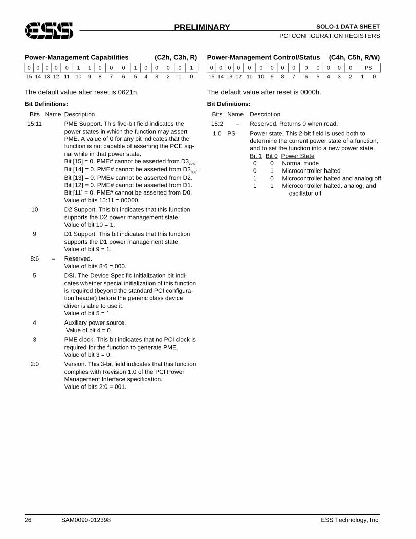
Power-Mana gement Capabilities (C2h, C3h, R)
The default value after reset is 0621h.
Bit Definitions:
Power-Mana gement Control/Status (C4h, C5h, R/W)
The default value after reset is 0000h.
Bit Definitions:
0 0 0 0 0 1 1 0 0 0 1 0 0 0 0 1
15 14 13 12 11 10 9 8 7 6 5 4 3 2 1 0
Bits Name Description
15:11 PME Support. This five-bit field indicates the power states in which the function may assert PME. A value of 0 for any bit indicates that the function is not capable of asserting the PCE sig-nal while in that power state.Bit [15] = 0. PME# cannot be asserted from D3cold.Bit [14] = 0. PME# cannot be asserted from D3hot.Bit [13] = 0. PME# cannot be asserted from D2.Bit [12] = 0. PME# cannot be asserted from D1.Bit [11] = 0. PME# cannot be asserted from D0.Value of bits 15:11 = 00000.
10 D2 Support. This bit indicates that this function supports the D2 power management state.Value of bit 10 = 1.
9 D1 Support. This bit indicates that this function supports the D1 power management state.Value of bit 9 = 1.
8:6 – Reserved.Value of bits 8:6 = 000.
5 DSI. The Device Specific Initialization bit indi-cates whether special initialization of this function is required (beyond the standard PCI configura-tion header) before the generic class device driver is able to use it.Value of bit 5 = 1.
4 Auxiliary power source. Value of bit 4 = 0.
3 PME clock. This bit indicates that no PCI clock is required for the function to generate PME.Value of bit 3 = 0.
2:0 Version. This 3-bit field indicates that this function complies with Revision 1.0 of the PCI Power Management Interface specification.Value of bits 2:0 = 001.
0 0 0 0 0 0 0 0 0 0 0 0 0 0 PS
15 14 13 12 11 10 9 8 7 6 5 4 3 2 1 0
Bits Name Description
15:2 – Reserved. Returns 0 when read.
1:0 PS Power state. This 2-bit field is used both to determine the current power state of a function, and to set the function into a new power state. Bit 1 Bit 0 Power State 0 0 Normal mode 0 1 Microcontroller halted 1 0 Microcontroller halted and analog off 1 1 Microcontroller halted, analog, and oscillator off

ESS Technology, Inc. SAM0090-012398 27
SOLO-1 DATA SHEET
I/O PORTSPRELIMINARY
I/O PORTS
Port Summary
Table 9 I/O Port Summary
PortRead/Write
Function
IO Device
IOBase+0h–IOBase+3h Read/write Audio 2 base/current DMA address.
IOBase+4h–IOBase+5h Read/write Audio 2 base/current DMA count.
IOBase+6h Read/write Solo-1 mode register.
IOBase+7h Read/write IRQ control register.
Audio/FM Device
SBBase+0h–SBBase+3h Read/write 20-voice FM synthesizer. Address and data registers.
SBBase+4h Read/write Mixer Address register (port for address of mixer controller registers).
SBBase+5h Read/write Mixer Data register (port for data to/from mixer controller registers).
SBBase+6h Read/write Audio reset and status flags.
SBBase+7h Read/write Power Management register. Suspend request and FM reset.
SBBase+8h–SBBase+9h Read/write 11-voice FM synthesizer. Address and data registers.
SBBase+Ah Read-only Input data from read buffer for command/data I/O. Poll bit 7 of port SBBase+Eh to test whether the read buffer contents are valid.
SBBase+Ch Read/write Output data to write buffer for command/data I/O. Read embedded processor status.
SBBase+Eh Read-only Data available flag from embedded processor.
SBBase+Fh Read/write Address for I/O access to FIFO in Extended mode.
MPU-401 Device
MPUBase+0h–MPUBase+1h Read/write MPU-401 port (x=0,1,2, or 3) if enabled.
Game Port Device
GPBase+1h Read/write Joystick.
DMAC Device
DDMABase+0h–DDMABase+2h Read/write DMA current/base address.
DDMABase+4h–DDMABase+5h Read/write DMA current/base count.
DDMABase+8h Read/write DMA command/status.
DDMABase+9h Write DMA request.
DDMABase+Bh Write DMA mode.
DDMABase+Dh Write DMA master clear.
DDMABase+Fh Read/write DMA mask.
28 SAM0090-012398 ESS Technology, Inc.
SOLO-1 DATA SHEET
I/O PORTSPRELIMINARY
Port Descriptions
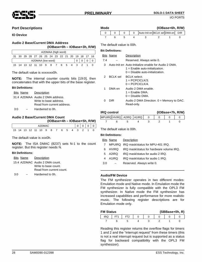
IO Device
Audio 2 Base/Current DMA Address(IOBase+0h – IOBase+3h, R/W)
The default value is xxxxxxx0h.
NOTE: The internal counter counts bits [19:0], thenconcatenates that with the upper bits of the base register.
Bit Definitions:
Audio 2 Base/Current DMA Count(IOBase+4h – IOBase+5h, R/W)
The default value is xxx0h.
NOTE: The ISA DMAC (8237) sets N-1 to the countregister. But this register needs N.
Bit Definitions:
Mode (IOBase+6h, R/W)
The default value is 00h.
Bit Definitions:
IRQ control (IOBase+7h, R/W)
The default value is 00h.
Bit Definitions:
Audio/FM DeviceThe FM synthesizer operates in two different modes:Emulation mode and Native mode. In Emulation mode theFM synthesizer is fully compatible with the OPL3 FMsynthesizer. In Native mode the FM synthesizer hasincreased capabilities and performance for more realisticmusic. The following register descriptions are forEmulation mode only.
FM Status (SBBase+0h, R)
Reading this register returns the overflow flags for timers1 and 2 and the “interrupt request” from these timers (thisis not a real interrupt request but is supported as a statusflag for backward compatibility with the OPL3 FMsynthesizer).
A2DMAA (high word)
31 30 29 28 27 26 25 24 23 22 21 20 19 18 17 16
A2DMAA (low word) 0 0 0 0
15 14 13 12 11 10 9 8 7 6 5 4 3 2 1 0
Bits Name Description
31:4 A2DMAA Audio 2 DMA address.Write to base address.Read from current address.
3:0 – Hardwired to 0h.
A2DMAC 0 0 0 0
15 14 13 12 11 10 9 8 7 6 5 4 3 2 1 0
Bits Name Description
15:4 A2DMAC Audio 2 DMA count.Write to base count.Read from current count.
3:0 – Hardwired to 0h.
0 0 0 0 Auto-Init en BCLK sel DMA en DIR
7 6 5 4 3 2 1 0
Bits Name Description
7:4 – Reserved. Always write 0.
3 Auto-Init en Auto-Initialize enable for Audio 2 DMA.1 = Enable auto-initialization.0 = Disable auto-initialization.
2 BCLK sel BCLK select.1 = PCPCICLK/3.0 = PCPCICLK/4.
1 DMA en Audio 2 DMA enable.1 = Enable DMA.0 = Disable DMA.
0 DIR Audio 2 DMA Direction. 0 = Memory to DAC.Read-only.
MPUIRQ HVIRQ A2IRQ A1IRQ 0 0 0 0
7 6 5 4 3 2 1 0
Bits Name Description
7 MPUIRQ IRQ mask/status for MPU-401 IRQ.
6 HVIRQ IRQ mask/status for hardware volume IRQ.
5 A2IRQ IRQ mask/status for audio 2 IRQ.
4 A1IRQ IRQ mask/status for audio 1 IRQ.
3:0 – Reserved. Always write 0.
IRQ FT1 FT2 0 0 0 0 0
7 6 5 4 3 2 1 0
ESS Technology, Inc. SAM0090-012398 29
SOLO-1 DATA SHEET
I/O PORTSPRELIMINARY
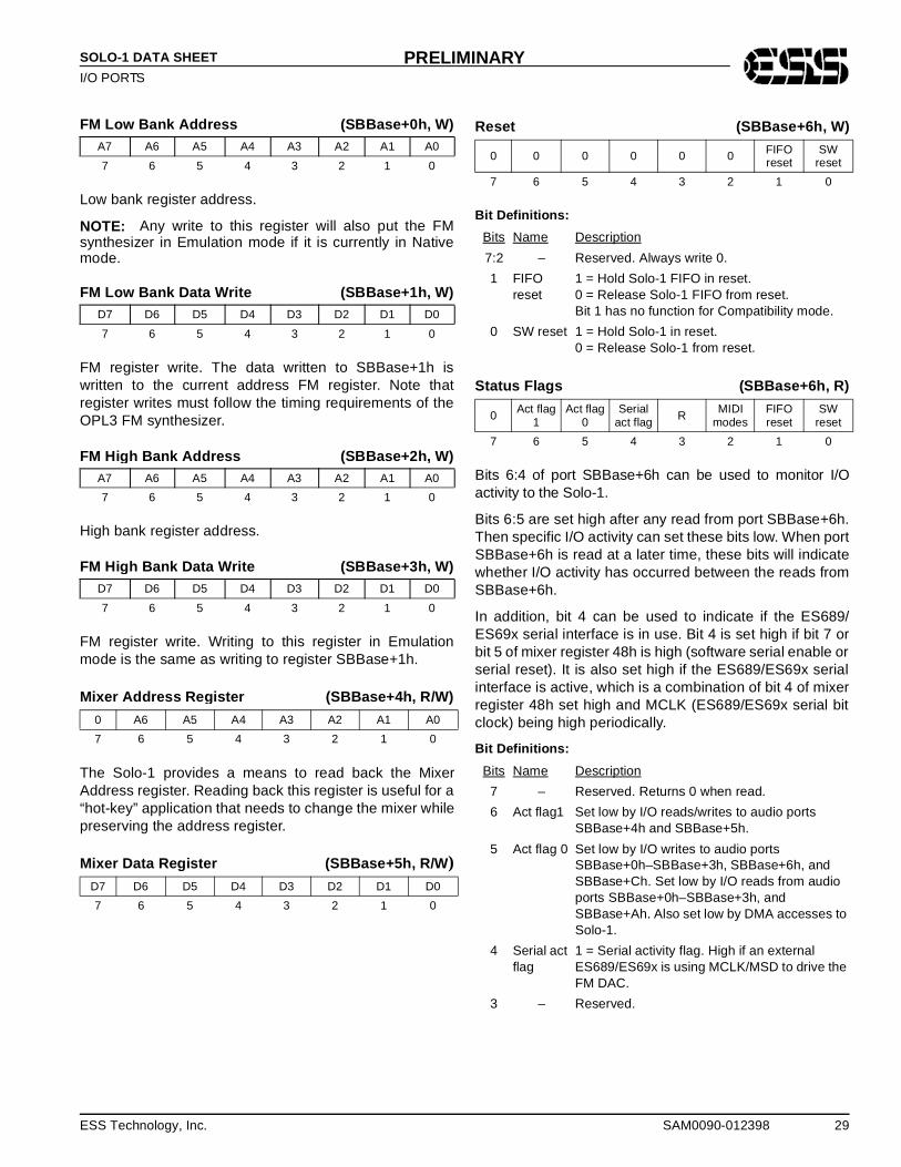
FM Low Bank Address (SBBase+0h, W)
Low bank register address.
NOTE: Any write to this register will also put the FMsynthesizer in Emulation mode if it is currently in Nativemode.
FM Low Bank Data Write (SBBase+1h, W)
FM register write. The data written to SBBase+1h iswritten to the current address FM register. Note thatregister writes must follow the timing requirements of theOPL3 FM synthesizer.
FM High Bank Address (SBBase+2h, W)
High bank register address.
FM High Bank Data Write (SBBase+3h, W)
FM register write. Writing to this register in Emulationmode is the same as writing to register SBBase+1h.
Mixer Address Re gister (SBBase+4h, R/W)
The Solo-1 provides a means to read back the MixerAddress register. Reading back this register is useful for a“hot-key” application that needs to change the mixer whilepreserving the address register.
Mixer Data Re gister (SBBase+5h, R/W )
Reset (SBBase+6h, W)
Bit Definitions:
Status Fla gs (SBBase+6h, R)
Bits 6:4 of port SBBase+6h can be used to monitor I/Oactivity to the Solo-1.
Bits 6:5 are set high after any read from port SBBase+6h.Then specific I/O activity can set these bits low. When portSBBase+6h is read at a later time, these bits will indicatewhether I/O activity has occurred between the reads fromSBBase+6h.
In addition, bit 4 can be used to indicate if the ES689/ES69x serial interface is in use. Bit 4 is set high if bit 7 orbit 5 of mixer register 48h is high (software serial enable orserial reset). It is also set high if the ES689/ES69x serialinterface is active, which is a combination of bit 4 of mixerregister 48h set high and MCLK (ES689/ES69x serial bitclock) being high periodically.
Bit Definitions:
A7 A6 A5 A4 A3 A2 A1 A0
7 6 5 4 3 2 1 0
D7 D6 D5 D4 D3 D2 D1 D0
7 6 5 4 3 2 1 0
A7 A6 A5 A4 A3 A2 A1 A0
7 6 5 4 3 2 1 0
D7 D6 D5 D4 D3 D2 D1 D0
7 6 5 4 3 2 1 0
0 A6 A5 A4 A3 A2 A1 A0
7 6 5 4 3 2 1 0
D7 D6 D5 D4 D3 D2 D1 D0
7 6 5 4 3 2 1 0
0 0 0 0 0 0 FIFO reset
SW reset
7 6 5 4 3 2 1 0
Bits Name Description
7:2 – Reserved. Always write 0.
1 FIFO reset
1 = Hold Solo-1 FIFO in reset.0 = Release Solo-1 FIFO from reset.Bit 1 has no function for Compatibility mode.
0 SW reset 1 = Hold Solo-1 in reset.0 = Release Solo-1 from reset.
0 Act flag 1
Act flag 0
Serial act flag R MIDI
modesFIFO reset
SW reset
7 6 5 4 3 2 1 0
Bits Name Description
7 – Reserved. Returns 0 when read.
6 Act flag1 Set low by I/O reads/writes to audio ports SBBase+4h and SBBase+5h.
5 Act flag 0 Set low by I/O writes to audio ports SBBase+0h–SBBase+3h, SBBase+6h, and SBBase+Ch. Set low by I/O reads from audio ports SBBase+0h–SBBase+3h, and SBBase+Ah. Also set low by DMA accesses to Solo-1.
4 Serial act flag
1 = Serial activity flag. High if an external ES689/ES69x is using MCLK/MSD to drive the FM DAC.
3 – Reserved.
30 SAM0090-012398 ESS Technology, Inc.
SOLO-1 DATA SHEET
I/O PORTSPRELIMINARY
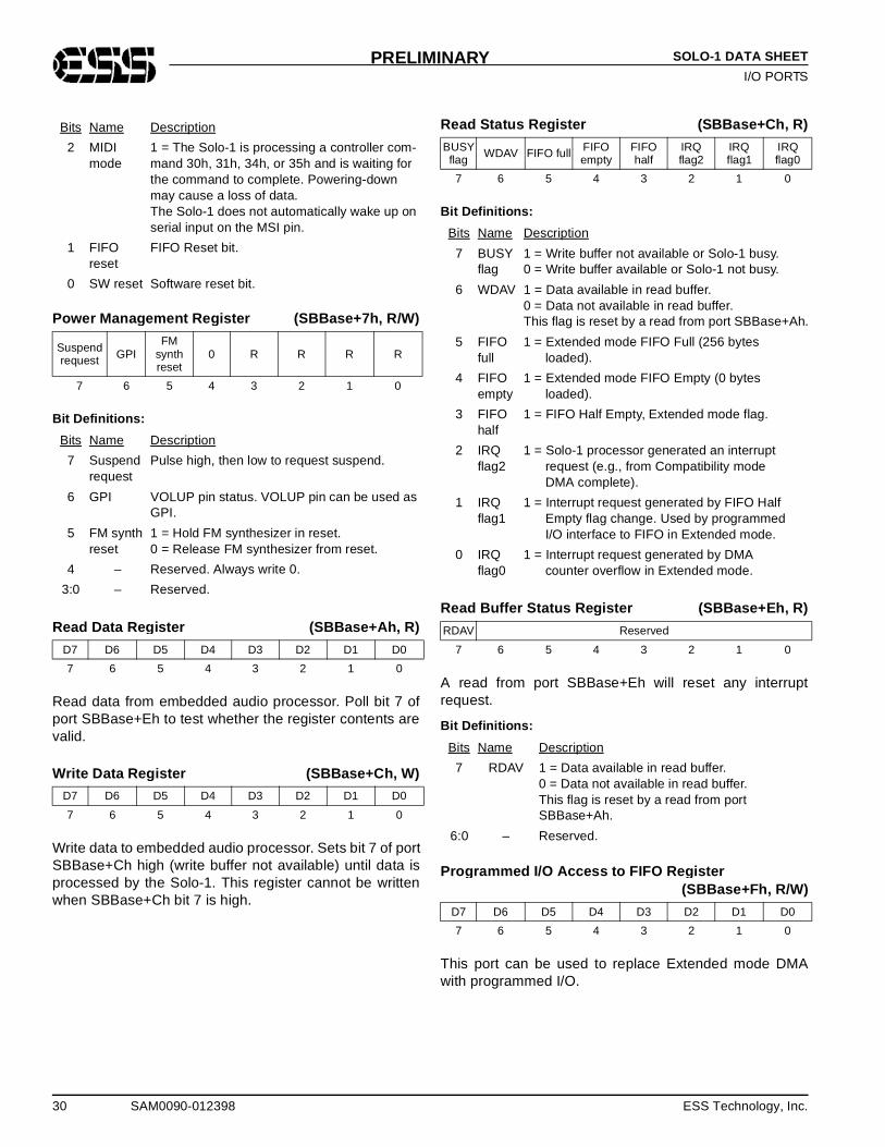
Power Mana gement Re gister (SBBase+7h, R/W)
Bit Definitions:
Read Data Register (SBBase+Ah, R)
Read data from embedded audio processor. Poll bit 7 ofport SBBase+Eh to test whether the register contents arevalid.
Write Data Re gister (SBBase+Ch, W)
Write data to embedded audio processor. Sets bit 7 of portSBBase+Ch high (write buffer not available) until data isprocessed by the Solo-1. This register cannot be writtenwhen SBBase+Ch bit 7 is high.
Read Status Re gister (SBBase+Ch, R)
Bit Definitions:
Read Buffer Status Re gister (SBBase+Eh, R)
A read from port SBBase+Eh will reset any interruptrequest.
Bit Definitions:
Programmed I/O Access to FIFO Re gister(SBBase+Fh, R/W)
This port can be used to replace Extended mode DMAwith programmed I/O.
2 MIDI mode
1 = The Solo-1 is processing a controller com-mand 30h, 31h, 34h, or 35h and is waiting for the command to complete. Powering-down may cause a loss of data.The Solo-1 does not automatically wake up on serial input on the MSI pin.
1 FIFO reset
FIFO Reset bit.
0 SW reset Software reset bit.
Suspend request GPI
FM synth reset
0 R R R R
7 6 5 4 3 2 1 0
Bits Name Description
7 Suspend request
Pulse high, then low to request suspend.
6 GPI VOLUP pin status. VOLUP pin can be used as GPI.
5 FM synth reset
1 = Hold FM synthesizer in reset.0 = Release FM synthesizer from reset.
4 – Reserved. Always write 0.
3:0 – Reserved.
D7 D6 D5 D4 D3 D2 D1 D0
7 6 5 4 3 2 1 0
D7 D6 D5 D4 D3 D2 D1 D0
7 6 5 4 3 2 1 0
Bits Name Description
BUSY flag WDAV FIFO full FIFO
emptyFIFO half
IRQ flag2
IRQ flag1
IRQ flag0
7 6 5 4 3 2 1 0
Bits Name Description
7 BUSY flag
1 = Write buffer not available or Solo-1 busy.0 = Write buffer available or Solo-1 not busy.
6 WDAV 1 = Data available in read buffer.0 = Data not available in read buffer.This flag is reset by a read from port SBBase+Ah.
5 FIFO full
1 = Extended mode FIFO Full (256 bytes loaded).
4 FIFO empty
1 = Extended mode FIFO Empty (0 bytes loaded).
3 FIFO half
1 = FIFO Half Empty, Extended mode flag.
2 IRQ flag2
1 = Solo-1 processor generated an interrupt request (e.g., from Compatibility mode DMA complete).
1 IRQ flag1
1 = Interrupt request generated by FIFO Half Empty flag change. Used by programmed I/O interface to FIFO in Extended mode.
0 IRQ flag0
1 = Interrupt request generated by DMA counter overflow in Extended mode.
RDAV Reserved
7 6 5 4 3 2 1 0
Bits Name Description
7 RDAV 1 = Data available in read buffer.0 = Data not available in read buffer.This flag is reset by a read from port SBBase+Ah.
6:0 – Reserved.
D7 D6 D5 D4 D3 D2 D1 D0
7 6 5 4 3 2 1 0
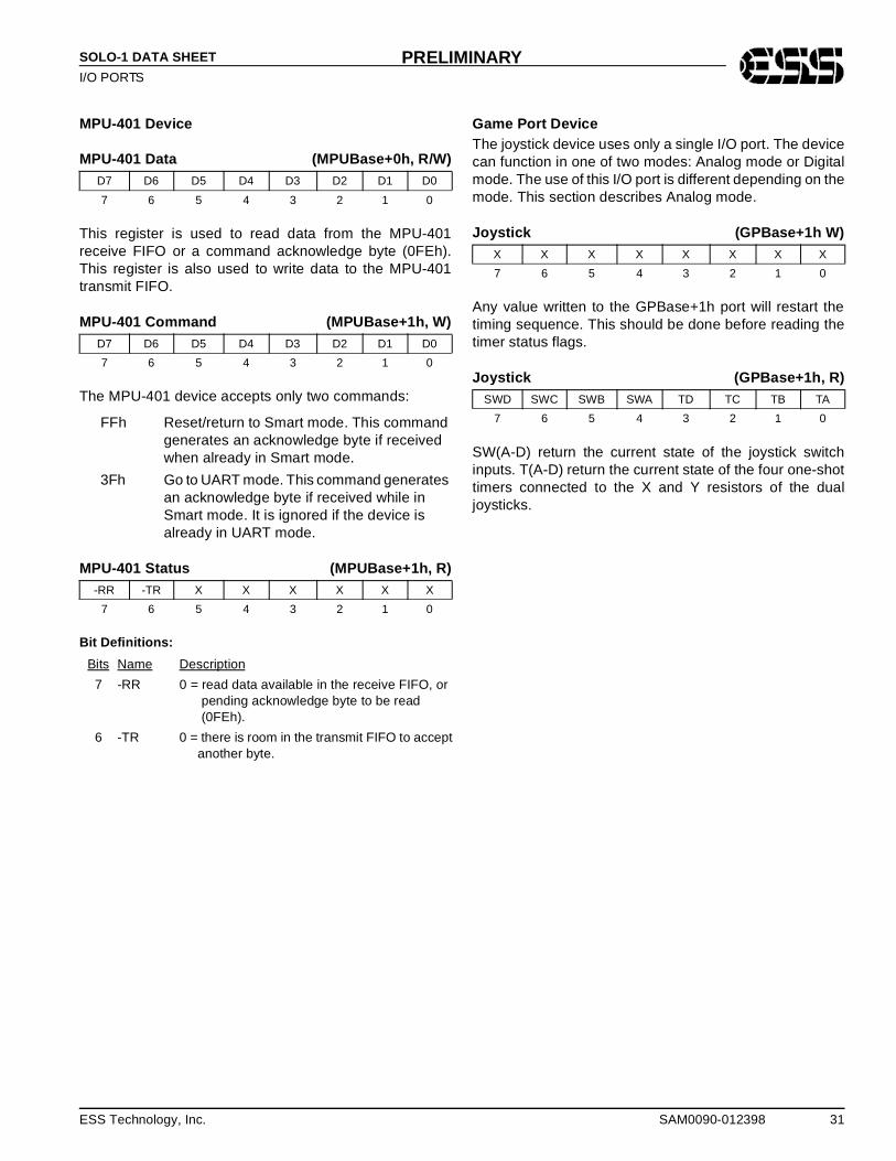
ESS Technology, Inc. SAM0090-012398 31
SOLO-1 DATA SHEET
I/O PORTSPRELIMINARY
MPU-401 Device
MPU-401 Data (MPUBase+0h, R/W)
This register is used to read data from the MPU-401receive FIFO or a command acknowledge byte (0FEh).This register is also used to write data to the MPU-401transmit FIFO.
MPU-401 Command (MPUBase+1h, W)
The MPU-401 device accepts only two commands:
FFh Reset/return to Smart mode. This command generates an acknowledge byte if received when already in Smart mode.
3Fh Go to UART mode. This command generates an acknowledge byte if received while in Smart mode. It is ignored if the device is already in UART mode.
MPU-401 Status (MPUBase+1h, R)
Bit Definitions:
Game Port DeviceThe joystick device uses only a single I/O port. The devicecan function in one of two modes: Analog mode or Digitalmode. The use of this I/O port is different depending on themode. This section describes Analog mode.
Joystick (GPBase+1h W)
Any value written to the GPBase+1h port will restart thetiming sequence. This should be done before reading thetimer status flags.
Joystick (GPBase+1h, R)
SW(A-D) return the current state of the joystick switchinputs. T(A-D) return the current state of the four one-shottimers connected to the X and Y resistors of the dualjoysticks.
D7 D6 D5 D4 D3 D2 D1 D0
7 6 5 4 3 2 1 0
D7 D6 D5 D4 D3 D2 D1 D0
7 6 5 4 3 2 1 0
-RR -TR X X X X X X
7 6 5 4 3 2 1 0
Bits Name Description
7 -RR 0 = read data available in the receive FIFO, or pending acknowledge byte to be read (0FEh).
6 -TR 0 = there is room in the transmit FIFO to accept another byte.
X X X X X X X X
7 6 5 4 3 2 1 0
SWD SWC SWB SWA TD TC TB TA
7 6 5 4 3 2 1 0
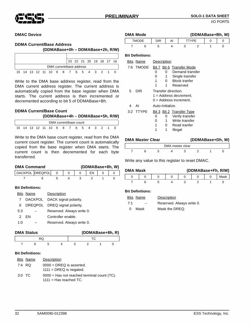
32 SAM0090-012398 ESS Technology, Inc.
SOLO-1 DATA SHEET
I/O PORTSPRELIMINARY
DMAC Device
DDMA Current/Base Address(DDMABase+0h – DDMABase+2h, R/W)
Write to the DMA base address register, read from theDMA current address register. The current address isautomatically copied from the base register when DMAstarts. The current address is then incremented ordecremented according to bit 5 of DDMABase+Bh.
DDMA Current/Base Count(DDMABase+4h – DDMABase+5h, R/W)
Write to the DMA base count register, read from the DMAcurrent count register. The current count is automaticallycopied from the base register when DMA starts. Thecurrent count is then decremented for each bytetransferred.
DMA Command (DDMABase+8h, W)
Bit Definitions:
DMA Status (DDMABase+8h, R)
Bit Definitions:
DMA Mode (DDMABase+Bh, W)
Bit Definitions:
DMA Master Clear (DDMABase+Dh, W)
Write any value to this register to reset DMAC.
DMA Mask (DDMABase+Fh, R/W)
Bit Definitions:
23 22 21 20 19 18 17 16
DMA current/base address
15 14 13 12 11 10 9 8 7 6 5 4 3 2 1 0
DMA current/base count
15 14 13 12 11 10 9 8 7 6 5 4 3 2 1 0
DACKPOL DREQPOL 0 0 0 EN 0 0
7 6 5 4 3 2 1 0
Bits Name Description
7 DACKPOL DACK signal polarity.
6 DREQPOL DREQ signal polarity.
5:3 – Reserved. Always write 0.
2 EN Controller enable.
1:0 – Reserved. Always write 0.
RQ TC
7 6 5 4 3 2 1 0
Bits Name Description
7:4 RQ 0000 = DREQ is asserted.1111 = DREQ is negated.
3:0 TC 0000 = Has not reached terminal count (TC).1111 = Has reached TC.
TMODE DIR AI TTYPE 0 0
7 6 5 4 3 2 1 0
Bits Name Description
7:6 TMODE Bit 7 Bit 6 Transfer Mode 0 0 Demand transfer 0 1 Single transfer 1 0 Block tranfer 1 1 Reserved
5 DIR Transfer direction.1 = Address decrement.0 = Address increment.
4 AI Auto-Initialize.
3:2 TTYPE Bit 3 Bit 2 Transfer Type 0 0 Verify transfer 0 1 Write transfer 1 0 Read tranfer 1 1 Illegal
DMA master clear
7 6 5 4 3 2 1 0
0 0 0 0 0 0 0 Mask
7 6 5 4 3 2 1 0
Bits Name Description
7:1 – Reserved. Always write 0.
0 Mask Mask the DREQ.
ESS Technology, Inc. SAM0090-012398 33
SOLO-1 DATA SHEET
PROGRAMMING THE SOLO-1PRELIMINARY
PROGRAMMING THE SOLO-1
Identifying the Solo-1
The Solo-1 device can be identified using the PCIstandard configuration register. Offset 0h contains theregistered Vendor ID (VID), which for ESS is 125Dh.Offset 2h contains the assigned Device ID (DID), which forthe Solo-1 is 1969h.
In addition, the Solo-1 has a Subsystem Vendor ID (SVID)and Subsystem ID (SID). These two registers default to125Dh and 1818h respectively at power-on. If the Solo-1is mounted on the motherboard, the BIOS can programthese two registers at startup. Note that warm reset doesnot reset these registers.
Resetting and Initializing the Solo-1
The Solo-1 chip can be reset in one of two ways: hardwareor software reset.
The hardware reset signal comes from the PCI bus and itinitializes:
• PCI configuration registers
• the microcontroller
• internal FIFOs
• the ESFM synthesizer
• the mixer registers
• the analog mixer
• CODECs
A cold reset also initializes SID/SVID (Subsystem ID andSubsystem Vendor ID) registers.
The software reset is controlled by bit 0 of portSBBase+6h and it initializes:
• the microcontroller
• the ESFM synthesizer
• the analog mixer
• the CODEC
To reset the Solo-1 by software:
1. Set bit 0 of SBBAase+6h.
2. Delay a short period by reading back SBBase+6h.
3. Clear bit 0 of SBBase+6h.
4. In a loop lasting at least 1 millisecond, poll port SBBase+Eh bit 7 for Read Data Available. Exit the loop only if bit 7 is high and SBBase+Ah returns 0AAh.
After the system powers up, the PCI BIOS initializes theheader portion (00h–3Fh) of the PCI configuration space.The PCI BIOS can also program the SID and SVIDregisters.
After the PCI BIOS initializes the device, the Solo-1 is innative mode. All of the PCI Configuration registers shouldbe set up properly before the Solo-1 accesses any otherregisters.
Table 10 Hardware and Software Reset Initializations
Initialization Hardware Reset Software Reset
Disable Extended Mode Yes Yes
Reset the timer divider and filter for 8 kHz Yes Yes
Stop any DMA transactions in progress Yes Yes
Clear any active interrupt requests Yes Yes
Disable voice input of mixer Yes Yes
Compatibility/Extended mode DMA counters to 2048 ytes Yes Yes
Set audio 1 CODEC direction to DAC Yes Yes
Set DAC volumes to mid-level Yes Yes
Set input volume for 8-bit recording with AGC to maximum Yes Yes
All other mixer registers to default values Yes No
Internal FIFO in extended mode Yes No2
PCI Configuration registers, except SID/SVID1 Yes No
1. SID/SVID can be initialized by power-up.2. Bit 1 of SBBase+6h can reset internal FIFOs.
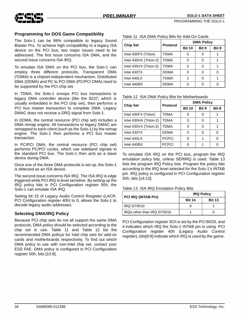
34 SAM0090-012398 ESS Technology, Inc.
SOLO-1 DATA SHEET
PROGRAMMING THE SOLO-1PRELIMINARY
Programming for DOS Game Compatibility
The Solo-1 can be 99% compatible to legacy SoundBlaster Pro. To achieve high compatibility to a legacy ISAdevice on the PCI bus, two major issues need to beaddressed. The first issue concerns ISA DMA, and thesecond issue concerns ISA IRQ.
To emulate ISA DMA on the PCI bus, the Solo-1 canemploy three different protocols. Transparent DMA(TDMA) is a chipset-independent mechanism, DistributedDMA (DDMA) and PC to PCI DMA (PC/PCI DMA) need tobe supported by the PCI chip set.
In TDMA, the Solo-1 snoops PCI bus transactions tolegacy DMA controller device (like the 8237, which isusually embedded in the PCI chip set), then performs aPCI bus master transaction to complete DMA. LegacyDMAC does not receive a DRQ signal from Solo-1.
In DDMA, the central resource (PCI chip set) includes aDMA remap engine. All transactions to legacy DMAC areremapped to each client (such as the Solo-1) by the remapengine. The Solo-1 then performs a PCI bus mastertransaction.
In PC/PCI DMA, the central resource (PCI chip set)performs PC/PCI cycles, which use sideband signals tothe standard PCI bus. The Solo-1 then acts as a slavedevice during DMA.
Once one of the three DMA protocols is set up, the Solo-1is detected as an ISA device.
The second issue concerns ISA IRQ. The ISA IRQ is edgetriggered while PCI IRQ is level sensitive. By setting up theIRQ policy bits in PCI Configuration register 50h, theSolo-1 can emulate ISA IRQ.
Setting bit 15 of Legacy Audio Control Rregister (LACR,PCI Configuration register 40h) to 0, allows the Solo-1 todecode legacy audio addresses.
Selecting DMA/IRQ Policy
Because PCI chip sets do not all support the same DMAprotocols, DMA policy should be selected according to thechip set in use. Table 11 and Table 12 list therecommended DMA policys for Intel chip sets for add-oncards and motherboards respectively. To find out whichDMA policy to use with non-Intel chip set, contact yourESS FAE. DMA policy is configured in PCI Configurationregister 50h, bits [10:8].
To emulate ISA IRQ on the PCI bus, program the IRQemulation policy bits, unless SERIRQ is used. Table 13lists the program IRQ Policy bits. Program the policy bitsaccording to the IRQ level selected for the Solo-1’s INTABpin. IRQ policy is configured in PCI Configuration register50h, bits [14:13].
PCI Configuration register 3Ch is set by the PCI BIOS, andit indicates which IRQ the Solo-1 INTAB pin is using. PCIConfiguration register 40h (Legacy Audio Controlregister), bits[9:8] indicate which IRQ is used by the game.
Table 11 ISA DMA Policy Bits for Add-On Cards
Chip Set ProtocolDMA Policy
Bit 10 Bit 9 Bit 8
Intel 430FX (Triton) TDMA 0 0 1
Intel 430HX (Triton-2) TDMA 0 0 1
Intel 430VX (Triton-3) TDMA 0 0 1
Intel 430TX DDMA 0 0 0
Intel 440LX TDMA’ 1 0 1
Intel 440BX DDMA 0 0 0
Table 12 ISA DMA Policy Bits for Motherboards
Chip Set ProtocolDMA Policy
Bit 10 Bit 9 Bit 8
Intel 430FX (Triton) TDMA 0 0 1
Intel 430HX (Triton-2) TDMA 0 0 1
Intel 430VX (Triton-3) TDMA 0 0 1
Intel 430TX DDMA 0 0 0
Intel 440LX PCPCI 0 1 0
Intel 440BX PCPCI 0 1 0
Table 13 ISA IRQ Emulation Policy Bits
PCI IRQ (INTAB Pin)IRQ Policy
Bit 14 Bit 13
IRQ 5/7/9/10 0 1
IRQs other than IRQ 5/7/9/10 1 0

ESS Technology, Inc. SAM0090-012398 35
SOLO-1 DATA SHEET
PROGRAMMING THE SOLO-1PRELIMINARY
Programming for Native PCI Audio
When the Solo-1 is configured as a native PCI device, theaudio channels must be configured properly, as shown inthe procedures below. The Solo-1 is a bus master device.
Confi gurin g Audio 1 in Native Mode
1. Set up the DDMA Control register.The PCI BIOS reserves IO regions (16 bytes), and stores them in the VCBase register. Copy the VCBase register (PCI Configuration register 18h) to the DDMA Control register (PCI Configuration register 60h), with bit 0 set.
2. Select the DMA/IRQ policy.The DMA policy should be set for DDMA (PCI Configuration register 50h, bits 10:8 = 000). The ISA IRQ emulation should be disabled (PCI Configuration register 50h, bits 14:13 = 00).
3. Program the Sound Blaster compatible module.See “Extended Mode Audio 1 DAC Operation” on page 40.
4. Program the DMA controller.Instead of using 8237 (DMAC), the program should use the built-in DMAC inside the Solo-1. The built-in DMAC is accessed as IO address range DDMABase+0h to DDMABase+Fh. Use the following sequence to program the built-in DMAC.
1. Master reset.Write any data to DDMABase+Dh.
2. Mask DMA.Write 1 to DDMABase+Fh.
3. Set up DMA mode.Write the mode value to DDMA Base+Bh.
4. Setup DMA base address and counts. Write the base address to DDMABase+0h.Write the base count to DDMABase+4h.
5. Unmask DMA.Write 0 to DDMABase+Fh.
Confi gurin g Audio 2 in Native Mode
Unlike programming for Audio 1 in native mode, all IOspaces are allocated by PCI BIOS.
1. Program the legacy ESS AudioDrive® controller module.See “Second Audio Channel DAC Operation” on page 43.
2. Program the DMA controller.Instead of using 8237 (DMAC), the program should use the built-in DMAC inside the Solo-1. The built-in DMAC is accessed as IO address range IOBase+0h to IOBase+6h. Use the following sequence to program the built-in DMAC.
1. Disable DMA.Clear bit 1 of IOBase+2h. Preserve all other bits.
2. Set up DMA mode.Program bit 3 of IOBase+2h. Preserve all other bits.
3. Set up DMA base address and counts.Write the base address to IOBase+0h.Write the base count to IOBase+4h.
4. Enable DMA.Set bit 1 of IOBase+2h. Preserve all other bits.
Modes of Operation
The Solo-1 can operate the first audio channel in one oftwo modes: Compatibility mode or Extended mode.
In both modes, a set of mixer and controller registersenables application software to control the analog mixer,record source, and output volume. Programming theSolo-1 Enhanced Mixer is described later in thisdocument. See “Programming the Solo-1 Mixer” onpage 45.
Compatibilit y Mode DescriptionThe first mode, Compatibility mode, is compatible to theSound Blaster Pro. This is the default mode after reset. Inthis mode, the Solo-1 microcontroller is an intermediary inall functions between the PCI bus and the CODEC. TheSolo-1 microcontroller performs limited FIFO functionsusing 64 bytes of internal memory.
Extended Mode DescriptionThe Solo-1 also supports an Extended mode of operation.In this case, a 256-byte FIFO is used as an intermediarybetween the PCI bus and the ADC and DAC Controlregisters, and various Extended mode controller registersare used for control. The Solo-1 microcontroller is mostlyidle in this mode. DMA control is handled by dedicatedlogic. Programming for Extended mode operation requiresaccessing various control registers with Solo-1commands.
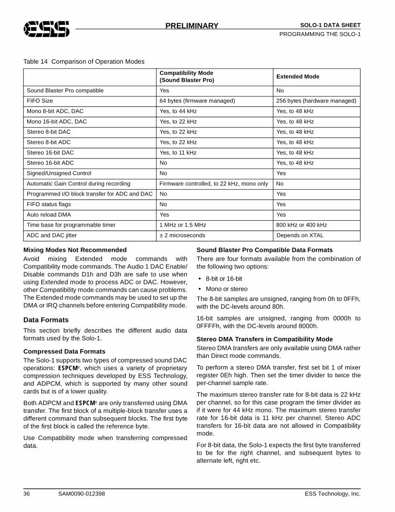
36 SAM0090-012398 ESS Technology, Inc.
SOLO-1 DATA SHEET
PROGRAMMING THE SOLO-1PRELIMINARY
Mixin g Modes Not RecommendedAvoid mixing Extended mode commands withCompatibility mode commands. The Audio 1 DAC Enable/Disable commands D1h and D3h are safe to use whenusing Extended mode to process ADC or DAC. However,other Compatibility mode commands can cause problems.The Extended mode commands may be used to set up theDMA or IRQ channels before entering Compatibility mode.
Data Formats
This section briefly describes the different audio dataformats used by the Solo-1.
Compressed Data FormatsThe Solo-1 supports two types of compressed sound DACoperations: ESPCM®, which uses a variety of proprietarycompression techniques developed by ESS Technology,and ADPCM, which is supported by many other soundcards but is of a lower quality.
Both ADPCM and ESPCM® are only transferred using DMAtransfer. The first block of a multiple-block transfer uses adifferent command than subsequent blocks. The first byteof the first block is called the reference byte.
Use Compatibility mode when transferring compresseddata.
Sound Blaster Pro Compatible Data FormatsThere are four formats available from the combination ofthe following two options:
• 8-bit or 16-bit
• Mono or stereo
The 8-bit samples are unsigned, ranging from 0h to 0FFh,with the DC-levels around 80h.
16-bit samples are unsigned, ranging from 0000h to0FFFFh, with the DC-levels around 8000h.
Stereo DMA Transfers in Compatibilit y ModeStereo DMA transfers are only available using DMA ratherthan Direct mode commands.
To perform a stereo DMA transfer, first set bit 1 of mixerregister 0Eh high. Then set the timer divider to twice theper-channel sample rate.
The maximum stereo transfer rate for 8-bit data is 22 kHzper channel, so for this case program the timer divider asif it were for 44 kHz mono. The maximum stereo transferrate for 16-bit data is 11 kHz per channel. Stereo ADCtransfers for 16-bit data are not allowed in Compatibilitymode.
For 8-bit data, the Solo-1 expects the first byte transferredto be for the right channel, and subsequent bytes toalternate left, right etc.
Table 14 Comparison of Operation Modes
Compatibility Mode(Sound Blaster Pro)
Extended Mode
Sound Blaster Pro compatible Yes No
FIFO Size 64 bytes (firmware managed) 256 bytes (hardware managed)
Mono 8-bit ADC, DAC Yes, to 44 kHz Yes, to 48 kHz
Mono 16-bit ADC, DAC Yes, to 22 kHz Yes, to 48 kHz
Stereo 8-bit DAC Yes, to 22 kHz Yes, to 48 kHz
Stereo 8-bit ADC Yes, to 22 kHz Yes, to 48 kHz
Stereo 16-bit DAC Yes, to 11 kHz Yes, to 48 kHz
Stereo 16-bit ADC No Yes, to 48 kHz
Signed/Unsigned Control No Yes
Automatic Gain Control during recording Firmware controlled, to 22 kHz, mono only No
Programmed I/O block transfer for ADC and DAC No Yes
FIFO status flags No Yes
Auto reload DMA Yes Yes
Time base for programmable timer 1 MHz or 1.5 MHz 800 kHz or 400 kHz
ADC and DAC jitter ± 2 microseconds Depends on XTAL

ESS Technology, Inc. SAM0090-012398 37
SOLO-1 DATA SHEET
PROGRAMMING THE SOLO-1PRELIMINARY
For 16-bit data, the Solo-1 expects DMA transfers to be amultiple of 4, with repeating groups in the order:
1. left low byte
2. left high byte
3. right low byte
4. right high byte
Solo-1 Data Formats (Extended Mode and Audio 2)There are eight formats available from the combination ofthe following three options:
• Mono or stereo
• 8-bit or 16-bit
• Signed or unsigned
For stereo data, the data stream always alternateschannels in successive samples: first left, then right. For16-bit data, the low byte always precedes the high byte.
Sendin g Commands Durin g DMA OperationsIt is useful to understand the detailed operation of sendinga command during DMA.
The Solo-1 uses the Audio 1 FIFO for DMA transfers to/from the CODEC. When the FIFO is full (in the case ofDAC) or empty (in the case of ADC), DMA requests aretemporarily suspended and the Busy flag (bit 7 of portSBBase+Ch) is cleared. This opens a window ofopportunity to send a command to the Solo-1. Commands
such as D1h and D3h which control the Audio 1 DACmixer input enable/disable status, and command D0h,which suspends or pauses DMA, are acceptable to sendduring this window.
The Solo-1 chip sets the Busy flag when the commandwindow is no longer open. Application software must senda command within 13 microseconds after the Busy flaggoes high or the command will be confused with DMAdata. Sending a command within the command window iseasy if polling is done with interrupts disabled.
As an example of sending a command during DMA,consider the case where the application wants to sendcommand D0h in the middle of a DMA transfer. Theapplication disables interrupts and polls the Busy flag.Because of the FIFO and the rules used for determiningthe command window, it is possible for the current DMAtransfer to complete while waiting for the Busy flag to clear.In this event, the D0h command has no function, and apending interrupt request from the DMA completion isgenerated.
The interrupt request can be cleared by reading portSBBase+Eh before enabling interrupts or having a way ofsignaling the interrupt handler that DMA is inactive so thatit does not try to start a new DMA transfer.
Figure 11 shows timing considerations for sending acommand.
Figure 11 Command Transfer Timing
Compatibility Mode Programming
This section describes Compatibility mode programming.
Compatibilit y Mode DAC Operation1. Reset
Write 1h to port SBBase+6h.
To play a new sound without resetting the Solo-1beforehand, when the status of the analog circuits isnot clear, mute the input to the mixer with commandD3h to prevent pops.
2. Enable stereo mode (optional).
Set bit 1 of mixer register 0Eh high. Use only DMAmode. Clear bit 1 of mixer register 0Eh after the DACtransfer.
3. Set sample rate and filter clock.
Use commands 40h or 41h to set the sample rate andfilter clock divider. To set the filter clock to beindependent from the sample rate, use command 42hin addition to 40h or 41h.
BUSY FLAG
POLL BUSY
WRITE COMMAND OK
WRITE COMMAND NOT OK
13 µsec
38 SAM0090-012398 ESS Technology, Inc.
SOLO-1 DATA SHEET
PROGRAMMING THE SOLO-1PRELIMINARY
For stereo transfers, set the timer divider to twice theper-channel sample rate. The maximum stereotransfer rate for 8-bit data is 22 kHz per channel; so forthis case, program the first timer divider as if you weretransferring data at 44 kHz mono. The maximum stereotransfer rate for 16-bit data is 11 kHz per channel.
4. Set the block size. Only use this command (48h) with High-Speed DMA transfer modes (commands 90h and 91h).
5. Configure the system interrupt controller and system DMA controller.
6. Start DMA.
Start the DMA transfer by sending the command for thedesired transfer type and data length. Theuncompressed modes are shown in Table 15. SeeTable 27 for a description of the commands in additionto the commands for DMA transfers of compresseddata.
7. Delay approximately 300 milliseconds to allow the analog circuits to settle, then enable the Audio 1 DAC input to mixer with command D1h.
8. During DMA.
For Auto-Initialize mode, it is not necessary to send anycommands to the Solo-1 at interrupt time, except toread SBBase+Eh to clear the interrupt request.
For Normal mode, initialize the system DMA controllerwith the address and count of the next block size if itchanges. Use command 48h. To start the next transfer,use command D4h.
To stop DMA after the current auto-initialize block isfinished, use command D0h.
Commands such as D1h and D3h, which control theAudio 1 DAC mixer input enable/disable status, andcommand D0h, which suspends DMA, are acceptableto send during DMA transfers. These commands can
only be sent during certain windows of opportunity. See“Stereo DMA Transfers in Compatibility Mode” onpage 36.
9. After DMA is finished, restore the system interrupt controller and DMA controller to their idle state. Monitor the FIFO Empty status flag in port SBBase+Ch to be sure that data transfer is completed. Delay 25 milliseconds to let the filter outputs settle to DC-levels, then disable the Audio 1 DAC input to the mixer with command D3h.
10.Issue another software reset to the Solo-1 to initialize the appropriate registers.
Compatibilit y Mode ADC Operation Solo-1 analog circuitry is switched from the DAC directionto the ADC direction by the first direct or DMA mode ADCcommand (2xh). Discard the first 25 to 100 milliseconds ofsamples because pops might occur in the data due to thechange from the DAC to ADC direction. In the ADCdirection the voice input to the mixer is automaticallymuted.
1. Reset
Write 1h to port SBBase+6h.
To play a new sound without resetting the Solo-1beforehand, when the status of the analog circuits isnot clear, mute the input to the mixer with commandD3h to prevent pops.
2. Select the input source using register 0Ch
Sound Blaster Pro has three recording sources:microphone, line, and auxiliary A (CD). Microphoneinput is the default source after any reset.
The Solo-1 has four recording sources: microphone,line, auxiliary A (CD), and mixer. Use mixer register1Ch to choose the additional source.
3. Program the input volume.
The selected source passes through an input volumestage that can be programmed with 16 levels of gainfrom 0 to +22.5 dB in steps of 1.5 dB. In 8-bitrecordings (other than High-Speed mode), the volumestage is controlled by the Solo-1 firmware for thepurposes of automatic gain control (AGC). In 16-bitrecordings as well as High-Speed mode 8-bitrecordings, the input volume stage is controllable fromapplication software. Use command DDh to changethe input volume level from 0 to 15. The reset default ismid-range, 8.
4. Enable stereo mode (optional).
Set bit 1 of mixer register 0Eh high. Use only DMAmode. Clear bit 1 of mixer register 0Eh after the ADCtransfer.
Table 15 Uncompressed DAC Transfer ModesDAC DMA Transfer Mode Data Length Command
Direct 8-bit 10h
16-bit 11h
DMA mode Normal 8-bit 14h
16-bit 15h
High-Speed 8-bit 91h
DMA mode Auto-Initialize 8-bit 1Ch
16-bit 1Dh
High-Speed 8-bit 90h

ESS Technology, Inc. SAM0090-012398 39
SOLO-1 DATA SHEET
PROGRAMMING THE SOLO-1PRELIMINARY
5. Set sample rate and filter clock.
Use commands 40h or 41h to set the sample rate andfilter clock divider. If you want to set the filter clock to beindependent from the sample rate, use command 42hin addition to 40h or 41h.
For stereo transfers, set the timer divider to twice theper-channel sample rate. The maximum stereotransfer rate for 8-bit data is 22 kHz per channel; so forthis case, program the first timer divider as if you weretransferring data at 44 kHz mono. The maximum stereotransfer rate for 16-bit data is 11 kHz per channel.
6. Set the block size. Only use this command (48h) with High-Speed DMA transfer modes (commands 98h and 99h).
7. Configure the system interrupt controller and system DMA controller.
8. Start DMA.
Start the DMA transfer by sending the command for thedesired transfer type and data length. Theuncompressed modes are shown in Table 16. SeeTable 27 for a description of the commands in additionto the commands for DMA transfers of compresseddata.
9. Delay approximately 100 milliseconds to allow the analog circuits to settle, then enable the Audio 1 DAC input to mixer with command D1h.
10.During DMA.
For Auto-Initialize mode, it is not necessary to send anycommands to the Solo-1 at interrupt time, except toread SBBase+Eh to clear the interrupt request.
For Normal mode, initialize the system DMA controllerwith the address and count of the next block size if itchanges. Use command 48h. To start the next transfer,use command D4h.
To stop DMA after the current auto-initialize block isfinished, use command D0h.
Commands such as D0h, which suspends DMA, areacceptable to send during DMA transfers. Thesecommands can only be sent during certain windows ofopportunity. See “Writing Commands to Solo-1Controller Registers” on page 40.
11.After DMA is finished, restore the system interrupt controller and DMA controller to their idle state. Monitor the FIFO Empty status flag in port SBBase+Ch to be sure that data transfer is completed.
12.Issue another software reset to the Solo-1 to initialize the appropriate registers.
The maximum sample rate for Direct mode ADC is 22 kHz.
The maximum sample rate for DMA ADC for both 8-bit and16-bit is 22 kHz, using commands 24h, 25h, 2Ch, or 2Dh.
There is a special High-Speed mode for ADC that allows8-bit sampling up to 44 kHz. This mode uses commands98h (auto-initialize) and 99h (normal). No AGC isperformed as the input volume is controlled with commandDDh.
Extended Mode Programming
This section describes Extended mode programming.
Commandin g Solo-1 Controller Re gistersController registers are written to and read from usingcommands sent to ports SBBase+Ch and SBBase+Ah.
Commands of the format Axh, Bxh, and Cxh, where x is anumeric value, are used for Extended mode programmingof the first audio channel.
Commands of the format Ax and Bx are used to accessthe Solo-1 controller registers. For convenience, theregisters are named after the commands used to accessthem. For example “register A4h,” the Audio 1 TransferCount Reload (low-byte) register, is written to by“command A4h.”
Enabling Extended Mode Commands
After any reset, and before using any Extended modecommands first send command C6h to enable Extendedmode commands.
Solo-1 Command/Data Handshakin g ProtocolThis section describes how to write commands to and readdata from the Solo-1 controller registers.
Table 16 Uncompressed ADC Transfer ModesADC DMA Transfer Mode Data Length Command
Direct 8-bit 20h
16-bit 21h
DMA mode Normal 8-bit 24h
16-bit 25h
High-Speed 8-bit 99h
DMA mode Auto-Initialize 8-bit 2Ch
16-bit 2Dh
High-Speed 8-bit 98h
40 SAM0090-012398 ESS Technology, Inc.
SOLO-1 DATA SHEET
PROGRAMMING THE SOLO-1PRELIMINARY
Writing Commands to Solo-1 Controller Registers
Commands written to the Solo-1 enter a write buffer.Before writing the command, make sure the buffer is notbusy.
Bit 7 of port SBBase+Ch is the Solo-1 Busy flag. It is setwhen the write buffer is full or when the Solo-1 is otherwisebusy (for example, during initialization after reset or duringCompatibility mode DMA requests).
To write a command or data byte to the Solo-1microcontroller:
1. Poll bit 7 of port SBBase+Ch until it is clear.
2. Write the command/data byte to port SBBase+Ch.
The following is an example of writing to Solo-1 controllerregisters. To set up the Audio 1 Transfer Count Reloadregister to F800h, send the following command/databytes:
A4h, 00h; register A4h = 0h
A5h, F8h; register A5h = F8h
NOTE: The port SBBase+Ch write buffer is shared withCompatibility mode DMA write operations. When DMA isactive, the Busy flag is cleared during windows of timewhen a command can be received. Normally, the onlycommands that should be sent during DMA operations areDxh commands such as DMA pause/continue and Audio1 DAC enable/disable. In this situation it is recommendedto disable interrupts between the time that the Busy bit ispolled and the command is written. Also, minimize the timebetween these instructions. See “Sending CommandsDuring DMA Operations” on page 37 for more information.
Reading the Read Data Buffer of the Solo-1
Command C0h is used to read the Solo-1 controllerregisters used for Extended mode. Send command C0hfollowed by the register number, Axh or Bxh. For example,to read register A4h, send the following command bytes:
C0h, A4h
Then poll the Read-Data-Buffer-Status bit, bit 7 of portSBBase+Eh, before reading the register contents fromport SBBase+Ah.
The Read-Data-Buffer-Status flag can be polled byreading bit 7 of port SBBase+Eh. When a byte is available,the bit is set high.
NOTE: Any read of port SBBase+Eh also clears anyactive interrupt request from the Solo-1. An alternate wayof polling the Read-Data-Buffer-Status bit is through bit 6of port SBBase+Ch, which is the same flag. The Read-Data-Buffer-Status flag is cleared automatically by readingthe byte from port SBBase+Ah.
Extended Mode Audio 1 DAC OperationFollow the steps below to program the first audio channelfor Extended mode DAC operation:
1. Reset
Write 3h to port SBBase+6h, instead of 1h as inCompatibility mode. Bit 1 high specifically clears theFIFO. The remainder of the software reset is identicalto Compatibility mode. Reset disables the Audio 1 DACinput to the mixer. This is intended to mask any popscreated during the setup of the DMA transfer.
2. After the reset, send command C6h to enable Extended mode commands.
3. Program direction and type: registers B8h, A8h, and B9h:
Register B8h: set bit 2 low for Normal DMA mode, highfor Auto-Initialize DMA mode. Leave bit 3 low for theCODEC to run in the DAC direction.
Register A8h: read this register to preserve the bits andthen modify only bits 1 and 0:
Bits 1:0 10: Mono
Bits 1:0 01: Stereo
Set register B9h:
Bits 1:0 00: Single transfer DMA.
Bits 1:0 01: Demand Transfer DMA: 2 bytes per DMA request.
Bits 1:0 11: Demand transfer DMA: 4 bytes per DMA request.
4. Clocks and counters: registers A1h, A2h, A4h and A5h:
Register A1h: Sample Rate Clock DividerRegister A2h: Filter Clock DividerRegisters A4h/A5h: Audio 1 Transfer Count Reloadregister low/high byte, two's complement
5. Initialize and configure DACs: registers B6h and B7h: See Table 17.
Register B6h: 80h for signed data and 00h for unsigneddata. This also initializes the CODEC for DAC transfer.
Register B7h: programs the FIFO (16-bit/8-bit, signed/unsigned, stereo/mono).

ESS Technology, Inc. SAM0090-012398 41
SOLO-1 DATA SHEET
PROGRAMMING THE SOLO-1PRELIMINARY
6. Enable/select DMA channel and IRQ channel, registers B1h, and B2h:
Register B1h: Interrupt Configuration register.Make sure bits 4 and 6 are high. Clear bits 7 and 5.
Register B2h: DRQ Configuration register.Make sure bits 4 and 6 are high. Clear bits 7 and 5.
7. Configure system interrupt controller and DMA controller.
8. To start DMA:
Set bit 0 of register B8h high while preserving all otherbits.
9. Delay approximately 100 milliseconds to allow analog circuits to settle, then enable the Audio 1 DAC input to mixer with command D1h.
10.During DMA
For Auto-Initialize transfers, read SBBase+Eh to clearthe interrupt request. Do not send any othercommands to the Solo-1 at interrupt time.
For Normal mode, initialize the system DMA controllerwith the address and count of the next block to transfer.Update the Solo-1 Transfer Count registers if the countis changed. To start the next transfer, clear bit 0 ofregister B8h, then set it high again.
To stop a DMA transaction in progress, clear bit 0 ofregister B8h. To stop a DMA transaction after thecurrent auto-initialize block is finished, clear bit 2 ofregister B8h, wait for the interrupt, and then clear bit 0of register B8h.
11.After DMA is finished:
Restore the system interrupt controller and DMAcontroller to their idle state. Monitor the FIFO Emptystatus flag in port SBBase+Ch to be sure data transferis completed. A delay of 25 milliseconds is required tolet the filter outputs settle to DC-levels, then disable thefirst DMA DAC input to the mixer with command D3h.
12.Finally:
Issue another software reset to the Solo-1 to initializethe appropriate registers.
Extended Mode Audio 1 ADC OperationFollow the steps below to program the first audio channelfor Extended mode ADC operation:
NOTE: In Extended mode, there is no Automatic GainControl (AGC) performed while recording. If AGC isnecessary, use 16-bit recordings and perform AGC insystem software.
1. Reset
Write 3h to port SBBase+6h instead of 1h as inCompatibility mode. Bit 1 high specifically clears theFIFO. The remainder of the software reset is identicalto Compatibility mode. Reset disables the Audio 1 DACinput to the mixer. This is intended to mask any popscreated during the setup of the DMA transfer.
2. Send command C6h to enable Extended mode commands.
3. Select the input source:
The Solo-1 has four recording sources: microphone,line, auxiliary A, and mixer. The mixer source can bethe playback mixer or the record mixer. Bits 4:3 ofmixer register 7Ah selects the mixer source. Therecord mixer is the default. Microphone input is thedefault after any reset. Select the source using themixer control register 1Ch.
4. Program input volume register B4h.
Table 17 Command Sequences for DMA Playback
Mono Stereo 8-bits 16-bits Unsigned Signed Sequence
X X X Reg B6h = 80h,Reg B7h = 51h,Reg B7h = D0h
X X X Reg B6h = 00h,Reg B7h = 71h,Reg B7h = F0h
X X X Reg B6h = 80h,Reg B7h = 51h,Reg B7h = D4h
X X X Reg B6h = 00h,Reg B7h = 71h,Reg B7h = F4h
X X X Reg B6h = 80h,Reg B7h = 51h,Reg B7h = 98h
X X X Reg B6h = 00h,Reg B7h = 71h,Reg B7h = B8h
X X X Reg B6h = 80h,Reg B7h = 51h,Reg B7h = 9Ch
X X X Reg B6h = 00h,Reg B7h = 71h,Reg B7h = BCh

42 SAM0090-012398 ESS Technology, Inc.
SOLO-1 DATA SHEET
PROGRAMMING THE SOLO-1PRELIMINARY
5. Program direction and type: registers B8h, and A8h:
Register B8h: set bit 3 high to program the CODEC forthe ADC direction. Set bit 2 low for Normal DMA mode,high for Auto-Initialize DMA mode.
At this point the direction of the analog circuits is ADCrather than DAC. Unless the recording monitor isenabled, there will be no output from AOUT_L orAOUT_R until the direction is restored to DAC.
Register A8h: read this register first to preserve the bitsand modify only bits 3, 1, and 0:
Bits 1:0 10: Mono
Bits 1:0 01: Stereo
Bit 3 0: Disable Record Monitor for now
Register B9h:
Bits 1:0 00: Single Transfer DMA
Bits 1:0 01: Demand Transfer: 2 bytes per DMA request
Bits 1:0 11: Demand Transfer: 4 bytes per DMA request
6. Clocks and counters: registers A1h, A2h, A4h and A5h:
Register A1h: Sample Rate Clock Divider. Set bit 7high for sample rates greater than 22 kHz.
Register A2h: Filter Clock Divider.
Registers A4h/A5h: Audio 1 Transfer Count Reloadregister low/high, two's complement
7. Delay 300 milliseconds to allow analog circuits to settle.
8. Enable Record Monitor if desired:
Register A8h bit 3 = 1: Enable Record Monitor(optional).
9. Initialize and configure ADC: register B7h. See Table 18. The first command sent to register B7h initializes the DAC and prevents pops.
Register B7h: programs the FIFO (16-bit/8-bit, signed/unsigned, stereo/mono).
10.Enable/select DMA channel and IRQ channel, registers B1h, and B2h:
Register B1h: Interrupt Configuration register.Verify that bits 4 and 6 are high. Clear bits 7 and 5.
Register B2h: DRQ Configuration register:Verify that bits 4 and 6 are high. Clear bits 7 and 5.
11.Configure system interrupt controller and DMA controller.
12.To start DMA:
Set bit 0 of register B8h high. Leave other bitsunchanged.
13.During DMA
For Auto-Initialize transfers, do not send anycommands to the Solo-1 at interrupt time, except forreading SBBase+Eh to clear the interrupt request.
For Normal mode, initialize the system DMA controllerwith the address and count of the next block to transfer.Update the Solo-1 Transfer Count registers if the countis changed. To start the next transfer, clear bit 0 ofregister B8h, then set it high again.
To stop a DMA transaction in progress, clear bit 0 ofregister B8h. To stop a DMA transaction after thecurrent auto-initialize block is finished, clear bit 2 ofregister B8h, wait for the interrupt, and then clear bit 0of register B8h.
14.After DMA is finished:
Restore the system interrupt controller and DMAcontroller to their idle state.
Table 18 Command Sequence for DMA Record
Mono Stereo 8-bits 16-bits Unsigned Signed Sequence
X X X Reg B7h = 51h,Reg B7h = D0h
X X X Reg B7h = 71h,Reg B7h = F0h
X X X Reg B7h = 51h,Reg B7h = D4h
X X X Reg B7h = 71h,Reg B7h = F4h
X X X Reg B7h = 51h,Reg B7h = 98h
X X X Reg B7h = 71h,Reg B7h = B8h
X X X Reg B7h = 51h,Reg B7h = 9Ch
X X X Reg B7h = 71h,Reg B7h = BCh
ESS Technology, Inc. SAM0090-012398 43
SOLO-1 DATA SHEET
PROGRAMMING THE SOLO-1PRELIMINARY
15.Finally:
Issue another software reset to the Solo-1 to initializethe appropriate registers. This returns the Solo-1 to theDAC direction and turns off the record monitor.
Extended Mode Pro grammed I/O OperationThe REP OUTSB instruction of the 80x86 family transfersdata from memory to an I/O port specified by the DXregister. The REP INSB instruction is the complementaryfunction. Use Solo-1 port SBBase+Fh for block transfers.
I/O transfers to FIFO are nearly identical to the DMAprocess, except that an I/O access to port SBBase+Fhreplaces the DMA cycle. Some differences are describedhere.
To program in this mode it is useful to understand how theFIFO Half-Empty flag generates an interrupt request. Aninterrupt request is generated on the rising edge of theFIFO Half-Empty flag. This flag can be polled by readingport SBBase+Ch. The meaning of this flag depends on thedirection of the transfer:
DAC FIFOHE flag is set high if 0-127 bytes in FIFO
ADC FIFOHE flag is set high if 128-256 bytes in FIFO
Therefore, for DAC operations, an interrupt request isgenerated when the number of bytes in the FIFO changesfrom >= 128 to < 128. This indicates to the systemprocessor that 128 bytes can be safely transferred withoutover-filling the FIFO. Before the first interrupt can begenerated, the FIFO needs to be primed, or filled, withmore than 128 bytes. Keep in mind that data may be takenout of the FIFO while it is being filled by the systemprocessor. If that is the case, there may never be >= 128bytes in the FIFO unless somewhat more than 128 bytesis transferred. Polling the Solo-1 FIFOHE flag to be sure itgoes low in the interrupt handler (or when priming theFIFO) and perhaps sending a second block of 128 bytesis a solution to this problem.
For ADC, the interrupt request is generated when thenumber of bytes in the FIFO changes from < 128 to >=128, indicating that the system processor can safely read128 bytes from the FIFO. Before the first interrupt can begenerated, the FIFO should be emptied (or mostly so) byreading from SBBase+Fh and polling the FIFOHE flag. Itis not safe to use FIFO reset bit 1 of port SBBase+6hindiscriminately to clear the FIFO, because it may get ADCdata out-of-sync.
As in DMA mode, bit 0 of register B8h enables transfersbetween the system and the FIFO inside the Solo-1.
NOTE: The Solo-1 is designed for I/O block transfer up toa ISA bus speed of 8.33 MHz.
Programmed I/O DAC Operation
Programmed I/O DAC operation is done just as explainedunder “Extended Mode Audio 1 DAC Operation” onpage 40 with the following exceptions:
• In step 3, programming register B9h is unnecessary.
• In step 6, leave bits 7:5 of register B2h low. Set bit 5 of register B1h high to enable an interrupt on FIFO half-empty transitions. Keep bit 6 of register B1h low.
• In step 8, in addition to setting bit 0 of register B8h high, send the REP OUTSB command.
Programmed I/O ADC Operation
Programmed I/O ADC operation is done just as explainedunder “Extended Mode Audio 1 ADC Operation” onpage 41 with the following exceptions:
• In step 3, programming register B9h is unnecessary.
• In step 6, leave bits 7:5 of register B2h low. Set bit 5 of register B1h high to enable an interrupt on FIFO half-empty transitions. Keep bit 6 of register B1h low.
• In step 8, in addition to setting bit 0 of register B8h high, send the REP OUTSB command.
Second Audio Channel DAC OperationFollow the steps below to program the second audiochannel for DAC operation.
1. Reset
Write 3h to port SBBase+6h, instead of 1h as inCompatibility mode. Bit 1 high specifically clears theFIFO. The remainder of the software reset is identicalto Compatibility mode. On reset the playback mixervolume for the second audio channel is set to zero,register 7Ch. This masks any pops that might occurduring the setup process.
2. Program transfer type: mixer register 78h:
Mixer register 78h: set bit 4 low for Normal DMA mode,high for Auto-Initialize DMA mode.
3. Clocks and counters: registers 70h, 72h, 74h and 76h:
Register 70h: Sample Rate GeneratorRegister 72h: Filter Clock DividerRegisters 74h/76h: Audio 2 Transfer Count Reload register low/high, two's complement
44 SAM0090-012398 ESS Technology, Inc.
SOLO-1 DATA SHEET
PROGRAMMING THE SOLO-1PRELIMINARY
4. Initialize and configure DAC: register 7Ah.
Register 7Ah:
Bit 2: set high for signed data, low for unsigned.
Bit 1: set high for stereo, low for mono.
Bit 0: set high for 16-bit samples, low for 8-bit.
5. Enable IRQ channel, register 7Ah and port IOBase+7h:
Register 7Ah: Audio 2 Control 2 register.Bit 6 unmasks channel 2 IRQ.
Port IOBase+7h: IRQ control register.Bit 5 unmasks channel 2 IRQ.
6. Program IOBase+0h, IOBase+4h, and IOBase+6h.
7. To start DMA:
Set bits 1:0 of register 78h high.
8. Delay approximately 100 milliseconds to allow analog circuits to settle, then enable the Audio 2 DAC playback volume, register 7Ch.
9. During DMA
For Auto-Initialize transfers, read SBBase+Eh to clearthe interrupt request. Do not send any othercommands to the Solo-1 at interrupt time.
For Normal mode, initialize IOBase+0h andIOBase+4h with the address and count of the nextblock to transfer. Update the Solo-1 Transfer Countregisters if the count is changed. To start the nexttransfer, clear bits 1:0 of register 78h, then set the bitshigh again.
To stop a DMA transaction in progress, clear bit 0 ofregister B8h. To stop a DMA transaction after thecurrent auto-initialize block is finished, clear bit 4 ofregister 78h, wait for the interrupt, and then clear bits1:0 of register 78h.
10.After DMA is finished:
Restore the system interrupt controller and DMAcontroller to their idle state. Monitor the FIFO Emptystatus flag in port SBBase+Ch to be sure data transferis completed. A delay of 25 milliseconds is required tolet the filter outputs settle to DC-levels, then disable theAudio 2 DAC input to the mixer.
11.Finally:
Issue another software reset to the Solo-1 to initializethe appropriate registers.
Full-Duplex DMA Mode
The Solo-1 supports stereo full-duplex DMA. In full-duplex(FD) mode, a second audio channel has been added tothe Solo-1. The second audio channel is programmedthrough mixer registers.
1. Program the first audio channel as in “Extended Mode Audio 1 ADC Operation” on page 41. Extended mode registers A1h and A2h define the sample rate and filter frequency for both record and playback. In other words, the record and playback must be at the same sample rate (synchronous).
2. Program the second audio channel. Mixer registers 74h and 76h are set to the two's complement DMA transfer count. The second audio channel supports both Auto-Initialize and Normal modes. The playback buffer in system memory does not have to be the same size as the record buffer. When the DMA transfer count rolls over to zero, it can generate an interrupt that is independent of the interrupt generated by the first audio channel.
If the record and playback buffers are the same size, thena single interrupt can be used. Program the DMA TransferCount Reload registers (A4h, A5h, 74h, and 76h) areprogrammed with the same value for both channels.Enable the second audio channel before enabling therecord channel. For example, assume there are two half-buffers in a circular buffer. When the record channelcompletes filling the first half, it generates an interrupt. Toensure that the playback channel is not accessing the firsthalf at the time of the interrupt, start the playback channelfirst. It has a 32-word FIFO that fills quickly through DMA.
The recommended method is as follows:
Program both DMA controllers for Auto-Initialize DMAwithin separate circular buffers of the same size, N.
To exit full-duplex mode, clear bits 0 and 1 of mixer register78h.
1. Reset
Write 3h to port SBBase+6h, instead of 1h as inCompatibility mode. Bit 1 high specifically clears theFIFO. The remainder of the software reset is identicalto Compatibility mode. Reset disables the Audio 1 DACinput to the mixer. This masks any pops created duringthe setup of the DMA transfer.
2. After the reset, send command C6h to enable Extended mode commands.
ESS Technology, Inc. SAM0090-012398 45
SOLO-1 DATA SHEET
PROGRAMMING THE SOLO-1PRELIMINARY
3. Program direction and type: registers B8h, A8h, and B9h:
Register B8h: set bit 2 high for Auto-Initialize DMAmode. Leave bit 3 low to program the CODEC for theDAC direction.
Register A8h: read this register first to preserve the bitsand modify only bits 3, 1, and 0:
Bits 1:0 10: Mono
Register B9h:
Bits 1:0 00: Single Transfer DMA
Bits 1:0 01: Demand Transfer DMA: 2 bytes per DMA request.
Bits 1:0 10: Demand transfer DMA: 4 bytes per DMA request.
4. Clocks and counters: registers A1h, A2h, A4h and A5h:
Register A1h: Sample Rate Clock DividerRegister A2h: Filter Clock DividerRegisters A4h/A5h: DMA Counter Reload register low/high, two's complement
5. Initialize and configure DAC: registers B6h and B7h.
Register B6h: 80h for signed data and 00h for unsigneddata. This also initializes the CODEC for DAC transfer.
Register B7h: set the data format for 16-bit mono. SeeTable 17, “Command Sequences for DMA Playback”on page 41.
6. Program transfer type: register 78h:
Register 78h: set bit 4 high for Auto-Initialize DMAmode.
7. Clocks and counters: registers 70h, 72h, 74h and 76h:
Set the sample rate the same as in A1h. Set theTransfer Count Reload to 64 bytes.
Register 70h: Sample Rate GeneratorRegister 72h: Filter Clock DividerRegisters 74h/76h: Second DMA Transfer Count Reload register low/high, two's complement
8. Initialize and configure DAC: register 7Ah.
Register 7Ah:
Bit 2: set high for signed data, low for unsigned.
Bit 1: set low for mono.
Bit 0: set high for 16-bit samples.
9. Enable IRQ channel, registers 7Ah and B2h:
Register 7Ah: Audio 2 Control 2 register.Bit 6 unmasks channel 2 IRQ.
Register B2h: DRQ Configuration register.Make sure bits 4 and 6 are high. Clear bits 7 and 5.
10.Set bit 0 of register 78h. Since the playback FIFO is presumably empty, the value zero is transferred to the playback DAC at each sample clock. A click or pop may be heard when full-duplex is enabled. To prevent this, use command D1h to enable the Audio 1 DAC input to the mixer after a suitable delay of 25 milliseconds.
11.Enable playback DMA by setting bit 1 of register 78h. After 64 bytes are transferred, bit 7 of 7Ah should go high. Poll this bit with a suitable time-out of 10 milliseconds.
12.After bit 7 of register 7Ah goes high, enable recording by setting bit 7 of register B7h and bit 0 of register B8h.
13.As usual, discard the first 50 to 100 milliseconds of recorded data until analog circuits have settled.
Programming the Solo-1 Mixer
The Solo-1 has a set of mixer registers that is backwardcompatible with the Sound Blaster Pro. However, some ofthe registers can be accessed in an “extended” or“alternate” way, providing for greater functionality.
Writin g and Readin g Data from the Mixer Re gistersThere are two I/O addresses used by the mixer:SBBase+4h is the address port; SBBase+5h is the dataport. In the Sound Blaster Pro, SBBase+4h is write only,while SBBase+5h is read/write.
Writing Data to the Solo-1 Mixer Registers
To set a mixer register, write its address to SBBase+4h,then write the data to SBBase+5h.
Reading Data from the Solo-1 Mixer Registers
To read the register, write its address to SBBase+4h, thenread the data from SBBase+5h.
Resettin g the Mixer Re gistersThe mixer registers are not affected by software reset. Toreset the registers to initial conditions, write any value tomixer register 00h:
1. Write 00h to SBBase+4h (select mixer register to 00h).
2. Write 00h to SBBase+5h (write 00h to the selected mixer register).
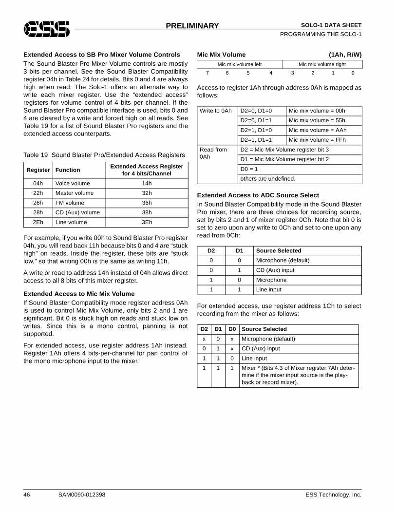
46 SAM0090-012398 ESS Technology, Inc.
SOLO-1 DATA SHEET
PROGRAMMING THE SOLO-1PRELIMINARY
Extended Access to SB Pro Mixer Volume ControlsThe Sound Blaster Pro Mixer Volume controls are mostly3 bits per channel. See the Sound Blaster Compatibilityregister 04h in Table 24 for details. Bits 0 and 4 are alwayshigh when read. The Solo-1 offers an alternate way towrite each mixer register. Use the “extended access”registers for volume control of 4 bits per channel. If theSound Blaster Pro compatible interface is used, bits 0 and4 are cleared by a write and forced high on all reads. SeeTable 19 for a list of Sound Blaster Pro registers and theextended access counterparts.
For example, if you write 00h to Sound Blaster Pro register04h, you will read back 11h because bits 0 and 4 are “stuckhigh” on reads. Inside the register, these bits are “stucklow,” so that writing 00h is the same as writing 11h.
A write or read to address 14h instead of 04h allows directaccess to all 8 bits of this mixer register.
Extended Access to Mic Mix VolumeIf Sound Blaster Compatibility mode register address 0Ahis used to control Mic Mix Volume, only bits 2 and 1 aresignificant. Bit 0 is stuck high on reads and stuck low onwrites. Since this is a mono control, panning is notsupported.
For extended access, use register address 1Ah instead.Register 1Ah offers 4 bits-per-channel for pan control ofthe mono microphone input to the mixer.
Mic Mix Volume (1Ah, R/W)
Access to register 1Ah through address 0Ah is mapped asfollows:
Extended Access to ADC Source SelectIn Sound Blaster Compatibility mode in the Sound BlasterPro mixer, there are three choices for recording source,set by bits 2 and 1 of mixer register 0Ch. Note that bit 0 isset to zero upon any write to 0Ch and set to one upon anyread from 0Ch:
For extended access, use register address 1Ch to selectrecording from the mixer as follows:
Table 19 Sound Blaster Pro/Extended Access Registers
Register FunctionExtended Access Register
for 4 bits/Channel
04h Voice volume 14h
22h Master volume 32h
26h FM volume 36h
28h CD (Aux) volume 38h
2Eh Line volume 3Eh
Mic mix volume left Mic mix volume right
7 6 5 4 3 2 1 0
Write to 0Ah D2=0, D1=0 Mic mix volume = 00h
D2=0, D1=1 Mic mix volume = 55h
D2=1, D1=0 Mic mix volume = AAh
D2=1, D1=1 Mic mix volume = FFh
Read from 0Ah
D2 = Mic Mix Volume register bit 3
D1 = Mic Mix Volume register bit 2
D0 = 1
others are undefined.
D2 D1 Source Selected
0 0 Microphone (default)
0 1 CD (Aux) input
1 0 Microphone
1 1 Line input
D2 D1 D0 Source Selected
x 0 x Microphone (default)
0 1 x CD (Aux) input
1 1 0 Line input
1 1 1 Mixer * (Bits 4:3 of Mixer register 7Ah deter-mine if the mixer input source is the play-back or record mixer).
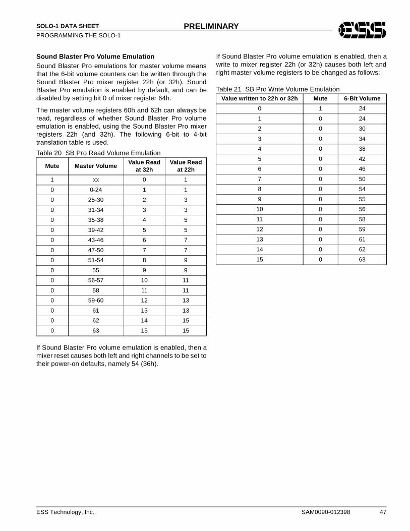
ESS Technology, Inc. SAM0090-012398 47
SOLO-1 DATA SHEET
PROGRAMMING THE SOLO-1PRELIMINARY
Sound Blaster Pro Volume EmulationSound Blaster Pro emulations for master volume meansthat the 6-bit volume counters can be written through theSound Blaster Pro mixer register 22h (or 32h). SoundBlaster Pro emulation is enabled by default, and can bedisabled by setting bit 0 of mixer register 64h.
The master volume registers 60h and 62h can always beread, regardless of whether Sound Blaster Pro volumeemulation is enabled, using the Sound Blaster Pro mixerregisters 22h (and 32h). The following 6-bit to 4-bittranslation table is used.
If Sound Blaster Pro volume emulation is enabled, then amixer reset causes both left and right channels to be set totheir power-on defaults, namely 54 (36h).
If Sound Blaster Pro volume emulation is enabled, then awrite to mixer register 22h (or 32h) causes both left andright master volume registers to be changed as follows:
Table 20 SB Pro Read Volume Emulation
Mute Master VolumeValue Read
at 32hValue Read
at 22h
1 xx 0 1
0 0-24 1 1
0 25-30 2 3
0 31-34 3 3
0 35-38 4 5
0 39-42 5 5
0 43-46 6 7
0 47-50 7 7
0 51-54 8 9
0 55 9 9
0 56-57 10 11
0 58 11 11
0 59-60 12 13
0 61 13 13
0 62 14 15
0 63 15 15
Table 21 SB Pro Write Volume EmulationValue written to 22h or 32h Mute 6-Bit Volume
0 1 24
1 0 24
2 0 30
3 0 34
4 0 38
5 0 42
6 0 46
7 0 50
8 0 54
9 0 55
10 0 56
11 0 58
12 0 59
13 0 61
14 0 62
15 0 63

48 SAM0090-012398 ESS Technology, Inc.
SOLO-1 DATA SHEET
PROGRAMMING THE SOLO-1PRELIMINARY
Record and Pla yback MixerThe Solo-1 has stereo mixers for playback and record.Each stereo mixer has eight input sources, each withindependent 4-bit left and right volume controls. For each4-bit volume control, level 0 is mute and level 15 ismaximum volume. The Solo-1 mixers use a dual slopemethod for selecting volume. Each increase of one step involume from settings 1 to 8 results in a +3 dB increase.Each increase of one step in volume from settings 8 to 15results in a +1.5 dB increase.
Table 22 Extended Access Mixer Volume Values
4-Bit Value
Volume in Decibels (dB)
Audio 1 a
(Record)
a. Audio 1 DAC mixer input is gated by the Sound Blaster“Speaker On” control. This control bit is toggled by the D1(on) and D3 (off) Sound Blaster commands.
Audio 2 b
(Playback)
b. In Telegaming mode (enabled by bit 0 of mixer register 48hwhen in Serial mode), the audio 2 DAC mixer input volumeis slaved to the audio 1 DAC mixer input volume.
Mic,Music DAC
AuxA, AuxB, Line,
Mono-In
15 +1.5 0 +10.5 +3.0
14 0 -1.5 +9.0 +1.5
13 -1.5 -3.0 +7.5 0
12 -3.0 -4.5 +6.0 -1.5
11 -4.5 -6.0 +4.5 -3.0
10 -6.0 -7.5 +3.0 -4.5
9 -7.5 -9.0 +1.5 -6.0
8 -9.0 -10.5 0 -7.5
7 -12.0 -13.5 -3.0 -10.5
6 -15.0 -16.5 -6.0 -13.5
5 -18.0 -19.5 -9.0 -16.5
4 -21.0 -22.5 -12.0 -19.5
3 -24.0 -25.5 -15.0 -22.5
2 -27.0 -28.5 -18.0 -25.5
1 -30.0 -31.5 -21.0 -28.5
0 mute mute mute mute
Table 23 Mixer Input Volume Registers
Mixer InputPlayback Volume
RegisterRecord Volume
Register
Audio 1 14h –
Audio 2 7Ch 69h
Microphone 1Ah 68h
Music DAC (FM/ES689/ES69x)
36h 6Bh
AuxA (CD) 38h 6Ah
AuxB 3Ah 6Ch
Line 3Eh 6Eh
Mono In 6Dh 6Fh
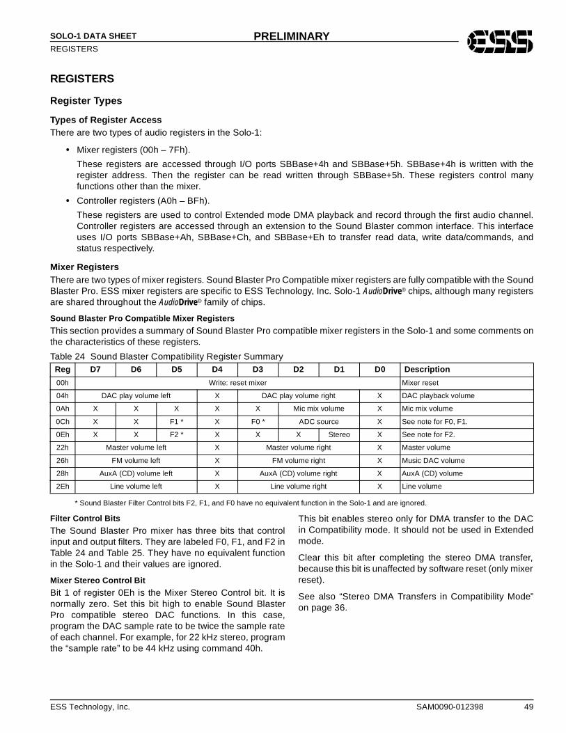
ESS Technology, Inc. SAM0090-012398 49
SOLO-1 DATA SHEET
REGISTERSPRELIMINARY
REGISTERS
Register Types
Types of Re gister AccessThere are two types of audio registers in the Solo-1:
• Mixer registers (00h – 7Fh).
These registers are accessed through I/O ports SBBase+4h and SBBase+5h. SBBase+4h is written with theregister address. Then the register can be read written through SBBase+5h. These registers control manyfunctions other than the mixer.
• Controller registers (A0h – BFh).
These registers are used to control Extended mode DMA playback and record through the first audio channel.Controller registers are accessed through an extension to the Sound Blaster common interface. This interfaceuses I/O ports SBBase+Ah, SBBase+Ch, and SBBase+Eh to transfer read data, write data/commands, andstatus respectively.
Mixer Re gistersThere are two types of mixer registers. Sound Blaster Pro Compatible mixer registers are fully compatible with the SoundBlaster Pro. ESS mixer registers are specific to ESS Technology, Inc. Solo-1 AudioDrive® chips, although many registersare shared throughout the AudioDrive® family of chips.
Sound Blaster Pro Compatible Mixer Registers
This section provides a summary of Sound Blaster Pro compatible mixer registers in the Solo-1 and some comments onthe characteristics of these registers.
* Sound Blaster Filter Control bits F2, F1, and F0 have no equivalent function in the Solo-1 and are ignored.
Filter Control Bits
The Sound Blaster Pro mixer has three bits that controlinput and output filters. They are labeled F0, F1, and F2 inTable 24 and Table 25. They have no equivalent functionin the Solo-1 and their values are ignored.
Mixer Stereo Control Bit
Bit 1 of register 0Eh is the Mixer Stereo Control bit. It isnormally zero. Set this bit high to enable Sound BlasterPro compatible stereo DAC functions. In this case,program the DAC sample rate to be twice the sample rateof each channel. For example, for 22 kHz stereo, programthe “sample rate” to be 44 kHz using command 40h.
This bit enables stereo only for DMA transfer to the DACin Compatibility mode. It should not be used in Extendedmode.
Clear this bit after completing the stereo DMA transfer,because this bit is unaffected by software reset (only mixerreset).
See also “Stereo DMA Transfers in Compatibility Mode”on page 36.
Table 24 Sound Blaster Compatibility Register SummaryReg D7 D6 D5 D4 D3 D2 D1 D0 Description
00h Write: reset mixer Mixer reset
04h DAC play volume left X DAC play volume right X DAC playback volume
0Ah X X X X X Mic mix volume X Mic mix volume
0Ch X X F1 * X F0 * ADC source X See note for F0, F1.
0Eh X X F2 * X X X Stereo X See note for F2.
22h Master volume left X Master volume right X Master volume
26h FM volume left X FM volume right X Music DAC volume
28h AuxA (CD) volume left X AuxA (CD) volume right X AuxA (CD) volume
2Eh Line volume left X Line volume right X Line volume
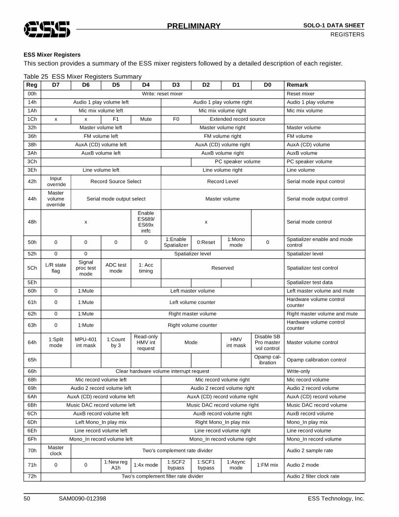
50 SAM0090-012398 ESS Technology, Inc.
SOLO-1 DATA SHEET
REGISTERSPRELIMINARY
ESS Mixer Registers
This section provides a summary of the ESS mixer registers followed by a detailed description of each register.
Table 25 ESS Mixer Registers Summary Reg D7 D6 D5 D4 D3 D2 D1 D0 Remark
00h Write: reset mixer Reset mixer
14h Audio 1 play volume left Audio 1 play volume right Audio 1 play volume
1Ah Mic mix volume left Mic mix volume right Mic mix volume
1Ch x x F1 Mute F0 Extended record source
32h Master volume left Master volume right Master volume
36h FM volume left FM volume right FM volume
38h AuxA (CD) volume left AuxA (CD) volume right AuxA (CD) volume
3Ah AuxB volume left AuxB volume right AuxB volume
3Ch PC speaker volume PC speaker volume
3Eh Line volume left Line volume right Line volume
42h Input override Record Source Select Record Level Serial mode input control
44hMaster volume override
Serial mode output select Master volume Serial mode output control
48h x
Enable ES689/ES69x
intfc
x Serial mode control
50h 0 0 0 0 1:Enable Spatializer 0:Reset 1:Mono
mode 0 Spatializer enable and mode control
52h 0 0 Spatializer level Spatializer level
5Ch L/R state flag
Signal proc test
mode
ADC test mode
1: Acc timing Reserved Spatializer test control
5Eh Spatializer test data
60h 0 1:Mute Left master volume Left master volume and mute
61h 0 1:Mute Left volume counter Hardware volume control counter
62h 0 1:Mute Right master volume Right master volume and mute
63h 0 1:Mute Right volume counter Hardware volume control counter
64h 1:Split mode
MPU-401int mask
1:Count by 3
Read-onlyHMV intrequest
Mode HMVint mask
Disable SB Pro master vol control
Master volume control
65h Opamp cal-ibration Opamp calibration control
66h Clear hardware volume interrupt request Write-only
68h Mic record volume left Mic record volume right Mic record volume
69h Audio 2 record volume left Audio 2 record volume right Audio 2 record volume
6Ah AuxA (CD) record volume left AuxA (CD) record volume right AuxA (CD) record volume
6Bh Music DAC record volume left Music DAC record volume right Music DAC record volume
6Ch AuxB record volume left AuxB record volume right AuxB record volume
6Dh Left Mono_In play mix Right Mono_In play mix Mono_In play mix
6Eh Line record volume left Line record volume right Line record volume
6Fh Mono_In record volume left Mono_In record volume right Mono_In record volume
70h Master clock Two’s complement rate divider Audio 2 sample rate
71h 0 0 1:New reg A1h 1:4x mode 1:SCF2
bypass1:SCF1 bypass
1:Async mode 1:FM mix Audio 2 mode
72h Two’s complement filter rate divider Audio 2 filter clock rate
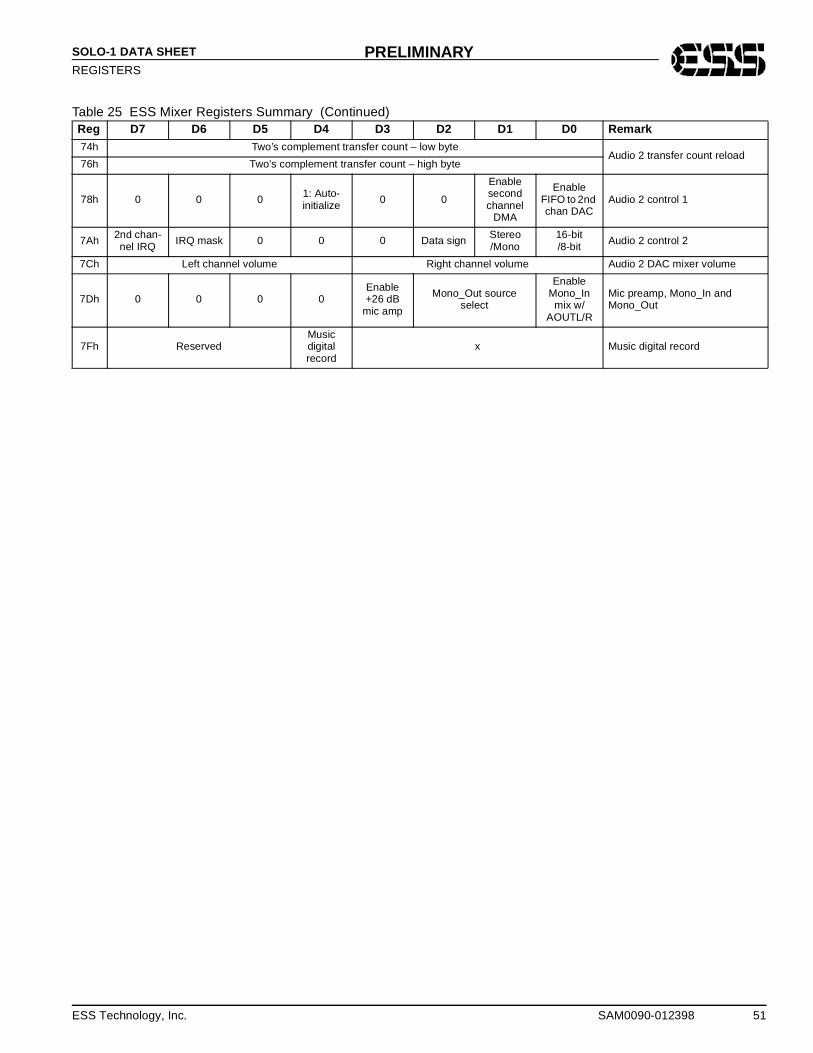
ESS Technology, Inc. SAM0090-012398 51
SOLO-1 DATA SHEET
REGISTERSPRELIMINARY
74h Two’s complement transfer count – low byteAudio 2 transfer count reload
76h Two’s complement transfer count – high byte
78h 0 0 0 1: Auto-initialize 0 0
Enable second channel
DMA
Enable FIFO to 2nd chan DAC
Audio 2 control 1
7Ah 2nd chan-nel IRQ IRQ mask 0 0 0 Data sign Stereo
/Mono16-bit/8-bit Audio 2 control 2
7Ch Left channel volume Right channel volume Audio 2 DAC mixer volume
7Dh 0 0 0 0Enable +26 dB
mic amp
Mono_Out source select
Enable Mono_In mix w/
AOUTL/R
Mic preamp, Mono_In and Mono_Out
7Fh ReservedMusic digital record
x Music digital record
Table 25 ESS Mixer Registers Summary (Continued)Reg D7 D6 D5 D4 D3 D2 D1 D0 Remark
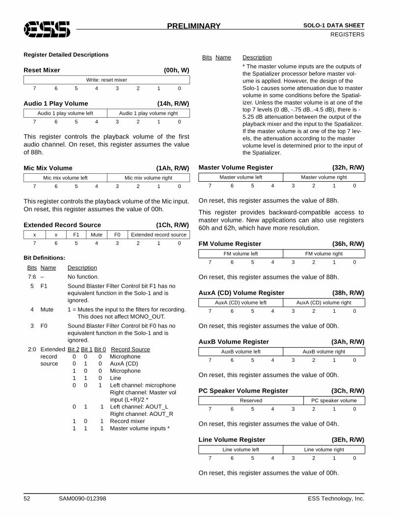
52 SAM0090-012398 ESS Technology, Inc.
SOLO-1 DATA SHEET
REGISTERSPRELIMINARY
Register Detailed Descriptions
Reset Mixer (00h, W)
Audio 1 Pla y Volume (14h, R/W)
This register controls the playback volume of the firstaudio channel. On reset, this register assumes the valueof 88h.
Mic Mix Volume (1Ah, R/W)
This register controls the playback volume of the Mic input.On reset, this register assumes the value of 00h.
Extended Record Source (1Ch, R/W)
Bit Definitions:
Master Volume Re gister (32h, R/W)
On reset, this register assumes the value of 88h.
This register provides backward-compatible access tomaster volume. New applications can also use registers60h and 62h, which have more resolution.
FM Volume Re gister (36h, R/W)
On reset, this register assumes the value of 88h.
AuxA (CD) Volume Re gister (38h, R/W)
On reset, this register assumes the value of 00h.
AuxB Volume Re gister (3Ah, R/W)
On reset, this register assumes the value of 00h.
PC Speaker Volume Re gister (3Ch, R/W)
On reset, this register assumes the value of 04h.
Line Volume Re gister (3Eh, R/W)
On reset, this register assumes the value of 00h.
Write: reset mixer
7 6 5 4 3 2 1 0
Audio 1 play volume left Audio 1 play volume right
7 6 5 4 3 2 1 0
Mic mix volume left Mic mix volume right
7 6 5 4 3 2 1 0
x x F1 Mute F0 Extended record source
7 6 5 4 3 2 1 0
Bits Name Description
7:6 – No function.
5 F1 Sound Blaster Filter Control bit F1 has no equivalent function in the Solo-1 and is ignored.
4 Mute 1 = Mutes the input to the filters for recording. This does not affect MONO_OUT.
3 F0 Sound Blaster Filter Control bit F0 has no equivalent function in the Solo-1 and is ignored.
2:0 Extended record source
Bit 2 Bit 1 Bit 0 Record Source 0 0 0 Microphone 0 1 0 AuxA (CD) 1 0 0 Microphone 1 1 0 Line 0 0 1 Left channel: microphone Right channel: Master vol input (L+R)/2 * 0 1 1 Left channel: AOUT_L Right channel: AOUT_R 1 0 1 Record mixer 1 1 1 Master volume inputs *
* The master volume inputs are the outputs of the Spatializer processor before master vol-ume is applied. However, the design of the Solo-1 causes some attenuation due to master volume in some conditions before the Spatial-izer. Unless the master volume is at one of the top 7 levels (0 dB, -.75 dB..-4.5 dB), there is -5.25 dB attenuation between the output of the playback mixer and the input to the Spatializer. If the master volume is at one of the top 7 lev-els, the attenuation according to the master volume level is determined prior to the input of the Spatializer.
Master volume left Master volume right
7 6 5 4 3 2 1 0
FM volume left FM volume right
7 6 5 4 3 2 1 0
AuxA (CD) volume left AuxA (CD) volume right
7 6 5 4 3 2 1 0
AuxB volume left AuxB volume right
7 6 5 4 3 2 1 0
Reserved PC speaker volume
7 6 5 4 3 2 1 0
Line volume left Line volume right
7 6 5 4 3 2 1 0
Bits Name Description
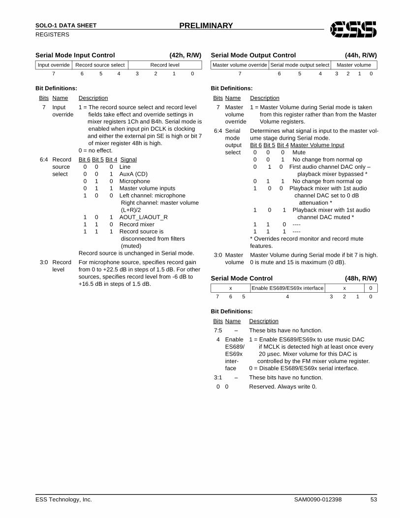
ESS Technology, Inc. SAM0090-012398 53
SOLO-1 DATA SHEET
REGISTERSPRELIMINARY
Serial Mode Input Control (42h, R/W)
Bit Definitions:
Serial Mode Output Control (44h, R/W)
Bit Definitions:
Serial Mode Control (48h, R/W)
Bit Definitions:
Input override Record source select Record level
7 6 5 4 3 2 1 0
Bits Name Description
7 Input override
1 = The record source select and record level fields take effect and override settings in mixer registers 1Ch and B4h. Serial mode is enabled when input pin DCLK is clocking and either the external pin SE is high or bit 7 of mixer register 48h is high.0 = no effect.
6:4 Record source select
Bit 6 Bit 5 Bit 4 Signal 0 0 0 Line 0 0 1 AuxA (CD) 0 1 0 Microphone 0 1 1 Master volume inputs 1 0 0 Left channel: microphone Right channel: master volume (L+R)/2 1 0 1 AOUT_L/AOUT_R 1 1 0 Record mixer 1 1 1 Record source is disconnected from filters (muted)Record source is unchanged in Serial mode.
3:0 Record level
For microphone source, specifies record gain from 0 to +22.5 dB in steps of 1.5 dB. For other sources, specifies record level from -6 dB to +16.5 dB in steps of 1.5 dB.
Master volume override Serial mode output select Master volume
7 6 5 4 3 2 1 0
Bits Name Description
7 Master volume override
1 = Master Volume during Serial mode is taken from this register rather than from the Master Volume registers.
6:4 Serial mode output select
Determines what signal is input to the master vol-ume stage during Serial mode.Bit 6 Bit 5 Bit 4 Master Volume Input 0 0 0 Mute 0 0 1 No change from normal op 0 1 0 First audio channel DAC only – playback mixer bypassed * 0 1 1 No change from normal op 1 0 0 Playback mixer with 1st audio channel DAC set to 0 dB attenuation * 1 0 1 Playback mixer with 1st audio channel DAC muted * 1 1 0 ---- 1 1 1 ----* Overrides record monitor and record mute features.
3:0 Master volume
Master Volume during Serial mode if bit 7 is high. 0 is mute and 15 is maximum (0 dB).
x Enable ES689/ES69x interface x 0
7 6 5 4 3 2 1 0
Bits Name Description
7:5 – These bits have no function.
4 Enable ES689/ES69xinter-face
1 = Enable ES689/ES69x to use music DAC if MCLK is detected high at least once every 20 µsec. Mixer volume for this DAC is controlled by the FM mixer volume register.0 = Disable ES689/ES69x serial interface.
3:1 – These bits have no function.
0 0 Reserved. Always write 0.
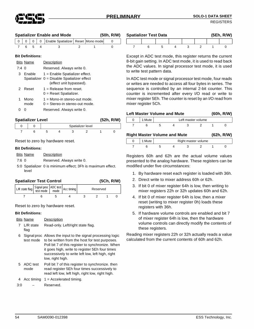
54 SAM0090-012398 ESS Technology, Inc.
SOLO-1 DATA SHEET
REGISTERSPRELIMINARY
Spatializer Enable and Mode (50h, R/W)
Bit Definitions:
Spatializer Level (52h, R/W)
Reset to zero by hardware reset.
Bit Definitions:
Spatializer Test Control (5Ch, R/W)
Reset to zero by hardware reset.
Bit Definitions:
Spatializer Test Data (5Eh, R/W)
Except in ADC test mode, this register returns the current8-bit gain setting. In ADC test mode, it is used to read backthe ADC values. In signal processor test mode, it is usedto write test pattern data.
In ADC test mode or signal processor test mode, four readsor writes are needed to access all four bytes in series. Thesequence is controlled by an internal 2-bit counter. Thiscounter is incremented after every I/O read or write tomixer register 5Eh. The counter is reset by an I/O read frommixer register 5Ch.
Left Master Volume and Mute (60h, R/W)
Right Master Volume and Mute (62h, R/W)
Registers 60h and 62h are the actual volume valuespresented to the analog hardware. These registers can bemodified under five circumstances:
1. By hardware reset each register is loaded with 36h.
2. Direct write to mixer address 60h or 62h.
3. If bit 0 of mixer register 64h is low, then writing to mixer registers 22h or 32h updates 60h and 62h.
4. If bit 0 of mixer register 64h is low, then a mixer reset (writing to mixer register 0h) loads these registers with 36h.
5. If hardware volume controls are enabled and bit 7 of mixer register 64h is low, then the hardware volume controls can directly modify the contents of these registers.
Reading mixer registers 22h or 32h actually reads a valuecalculated from the current contents of 60h and 62h.
0 0 0 0 Enable Spatializer Reset Mono mode 0
7 6 5 4 3 2 1 0
Bits Name Description
7:4 0 Reserved. Always write 0.
3 Enable Spatializer
1 = Enable Spatializer effect.0 = Disable Spatializer effect (effect unit bypassed).
2 Reset 1 = Release from reset.0 = Reset Spatializer.
1 Mono mode
1 = Mono-in stereo-out mode.0 = Stereo-in stereo-out mode.
0 0 Reserved. Always write 0.
0 0 Spatializer level
7 6 5 4 3 2 1 0
Bits Name Description
7:6 0 Reserved. Always write 0.
5:0 Spatializerlevel
0 is minimum effect; 3Fh is maximum effect.
L/R state flag Signal proc test mode
ADC test mode Acc timing Reserved
7 6 5 4 3 2 1 0
Bits Name Description
7 L/R state flag
Read-only. Left/right state flag.
6 Signal proc test mode
Allows the input to the signal processing logic to be written from the host for test purposes. Poll bit 7 of this register to synchronize. When it goes high, write to register 5Eh four times successively to write left low, left high, right low, right high.
5 ADC test mode
Poll bit 7 of this register to synchronize. then read register 5Eh four times successively to read left low, left high, right low, right high.
4 Acc timing 1 = Accelerated timing.
3:0 – Reserved.
7 6 5 4 3 2 1 0
0 1:Mute Left master volume
7 6 5 4 3 2 1 0
0 1:Mute Right master volume
7 6 5 4 3 2 1 0

ESS Technology, Inc. SAM0090-012398 55
SOLO-1 DATA SHEET
REGISTERSPRELIMINARY
Left Hardware Volume Control Counter (61h, R/W)
See the explanation following the Right Hardware VolumeControl Counter, mixer register 63h.
Right Hardware Volume Control Counter (63h, R/W)
These registers only exist if bit 7 of mixer register 64h ishigh. If bit 7 is low, these registers are combined withregisters 60h and 62h and cannot be independentlywritten or read.
If bit 7 of mixer register 64h is high, these registers haveno connection with registers 60h or 62h. They are thehardware volume counters and mute. It is theresponsibility of the host software to read these registersand update the master volume registers 60h and 62h.
Master Volume Control (64h, R/W)
Bit Definitions:
Opamp Calibration Control (65h, R/W)
In the analog circuitry of the Solo-1, operational amplifiersthat require calibration go through a calibration procedurethat takes about 200 milliseconds to perform. During thisperiod the analog outputs of the chip (AOUT_L, AOUT_R,and MONO_OUT) are muted.
The calibration procedure occurs automatically afterhardware reset and can be started at any time thereafterby writing 1 to mixer register 65h.
Bit Definitions:
Clear Hardware Volume Interrupt Request (66h, R/W)
Any write to this register resets the hardware volumeinterrupt request.
Mic Record (68h, R/W)
0 1:Mute Left volume counter
7 6 5 4 3 2 1 0
0 1:Mute Right volume counter
7 6 5 4 3 2 1 0
Split mode
MPU-401 int mask
Count by 3
Read-only HMV int request Mode HMV int
maskDisable SB Pro master
vol emulation
7 6 5 4 3 2 1 0
Bits Name Description
7 Split mode
1 = Split counter registers from volume registers and access them independently.0 = Slave counter and volume registers together.
6 MPU-401 int mask
This bit is AND'ed with the MPU-401 interrupt request. If it is low, the MPU-401 interrupt request stays low. This bit is cleared by hardware reset.
5 Count by 3
1 = Count up and down by 3 for each push of Up or Down buttons.0 = Count up and down by 1 for each push of Up or Down buttons.This bit is cleared by hardware reset.
4 Read-only HMV int request
Read-only interrupt request from hardware volume event.
3:2 Mode Selects operation mode:Bit 3 Bit 2 Operating Mode 0 0 Reserved 0 1 2-wire mode: both Up and Down inputs being low together act the same as Mute input low. 1 0 Reduced debounce (10 µsec vs. 40 msec), 2-wire mode, auto-increment and decrement disabled. 1 1 Hardware volume control disabled
1 HMV int mask
This bit is AND'ed with the hardware volume interrupt request before being OR'd with the first channel audio interrupt request. If this bit is low, the hardware volume interrupt request does not get OR'd with the first channel audio interrupt request. This bit is cleared by hardware reset.
0 Disable SB Pro master vol emula-tion
When low, a write to Sound Blaster Pro master volume registers 22h or 32h is translated into a write to hardware master volume registers 60h and 62h. Also, if low, a mixer reset (writing to mixer register 0h) causes registers 60h and 62h to be reset to default value 36h.When high, the Sound Blaster Pro master volume registers are, in effect, read-only.This bit is cleared by hardware reset.
Opamp calibration
7 6 5 4 3 2 1 0
Bits Name Description
0 Opamp calibration
Read: 1 = Opamp calibration is in progress. The calibration operation happens after hardware reset if a 1 is written to this bit. Calibration takes about 200 msec, during which the analog outputs of the chip (AOUT_L/R, MONO_OUT) are muted.Write: A 1 written to this register starts a calibration operation. A zero written to this register stops the calibration operation immediately (not recommended).
Clear Hardware Master Control
7 6 5 4 3 2 1 0
Left Mic record Right Mic record
7 6 5 4 3 2 1 0
Bits Name Description
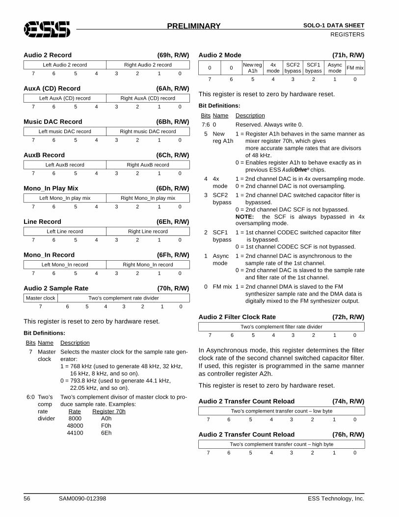
56 SAM0090-012398 ESS Technology, Inc.
SOLO-1 DATA SHEET
REGISTERSPRELIMINARY
Audio 2 Record (69h, R/W)
AuxA (CD) Record (6Ah, R/W)
Music DAC Record (6Bh, R/W)
AuxB Record (6Ch, R/W)
Mono_In Pla y Mix (6Dh, R/W)
Line Record (6Eh, R/W)
Mono_In Record (6Fh, R/W)
Audio 2 Sample Rate (70h, R/W)
This register is reset to zero by hardware reset.
Bit Definitions:
Audio 2 Mode (71h, R/W)
This register is reset to zero by hardware reset.
Bit Definitions:
Audio 2 Filter Clock Rate (72h, R/W)
In Asynchronous mode, this register determines the filterclock rate of the second channel switched capacitor filter.If used, this register is programmed in the same manneras controller register A2h.
This register is reset to zero by hardware reset.
Audio 2 Transfer Count Reload (74h, R/W)
Audio 2 Transfer Count Reload (76h, R/W)
Left Audio 2 record Right Audio 2 record
7 6 5 4 3 2 1 0
Left AuxA (CD) record Right AuxA (CD) record
7 6 5 4 3 2 1 0
Left music DAC record Right music DAC record
7 6 5 4 3 2 1 0
Left AuxB record Right AuxB record
7 6 5 4 3 2 1 0
Left Mono_In play mix Right Mono_In play mix
7 6 5 4 3 2 1 0
Left Line record Right Line record
7 6 5 4 3 2 1 0
Left Mono_In record Right Mono_In record
7 6 5 4 3 2 1 0
Master clock Two’s complement rate divider
7 6 5 4 3 2 1 0
Bits Name Description
7 Master clock
Selects the master clock for the sample rate gen-erator:1 = 768 kHz (used to generate 48 kHz, 32 kHz, 16 kHz, 8 kHz, and so on).0 = 793.8 kHz (used to generate 44.1 kHz, 22.05 kHz, and so on).
6:0 Two’s comp rate divider
Two’s complement divisor of master clock to pro-duce sample rate. Examples: Rate Register 70h 8000 A0h 48000 F0h 44100 6Eh
0 0 New reg A1h
4x mode
SCF2 bypass
SCF1 bypass
Async mode FM mix
7 6 5 4 3 2 1 0
Bits Name Description
7:6 0 Reserved. Always write 0.
5 New reg A1h
1 = Register A1h behaves in the same manner as mixer register 70h, which gives more accurate sample rates that are divisors of 48 kHz.0 = Enables register A1h to behave exactly as in previous ESS AudioDrive® chips.
4 4x mode
1 = 2nd channel DAC is in 4x oversampling mode.0 = 2nd channel DAC is not oversampling.
3 SCF2 bypass
1 = 2nd channel DAC switched capacitor filter is bypassed.0 = 2nd channel DAC SCF is not bypassed.NOTE: the SCF is always bypassed in 4xoversampling mode.
2 SCF1 bypass
1 = 1st channel CODEC switched capacitor filter is bypassed.0 = 1st channel CODEC SCF is not bypassed.
1 Async mode
1 = 2nd channel DAC is asynchronous to the sample rate of the 1st channel.0 = 2nd channel DAC is slaved to the sample rate and filter rate of the 1st channel.
0 FM mix 1 = 2nd channel DMA is slaved to the FM synthesizer sample rate and the DMA data is digitally mixed to the FM synthesizer output.
Two’s complement filter rate divider
7 6 5 4 3 2 1 0
Two’s complement transfer count – low byte
7 6 5 4 3 2 1 0
Two’s complement transfer count – high byte
7 6 5 4 3 2 1 0
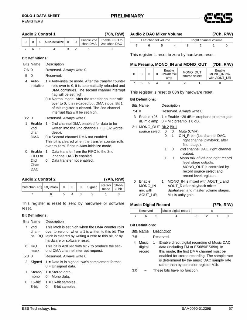
ESS Technology, Inc. SAM0090-012398 57
SOLO-1 DATA SHEET
REGISTERSPRELIMINARY
Audio 2 Control 1 (78h, R/W)
Bit Definitions:
Audio 2 Control 2 (7Ah, R/W)
This register is reset to zero by hardware or softwarereset.
Bit Definitions:
Audio 2 DAC Mixer Volume (7Ch, R/W)
This register is reset to zero by hardware reset.
Mic Preamp, MONO_IN and MONO_OUT (7Dh, R/W)
This register is reset to 08h by hardware reset.
Bit Definitions:
Music Di gital Record (7Fh, R/W)
Bit Definitions:
0 0 0 Auto-initialize 0 0 Enable 2nd chan DMA
Enable FIFO to 2nd chan DAC
7 6 5 4 3 2 1 0
Bits Name Description
7:6 0 Reserved. Always write 0.
5 0 Reserved.
4 Auto-initialize
1 = Auto-initialize mode. After the transfer counter rolls over to 0, it is automatically reloaded and DMA continues. The second channel interrupt flag will be set high.0 = Normal mode. After the transfer counter rolls over to 0, it is reloaded but DMA stops. Bit 1 of this register is cleared. The 2nd channel interrupt flag will be set high.
3:2 0 Reserved. Always write 0.
1 Enable 2nd chan DMA
1 = 2nd channel DMA enabled for data to be written into the 2nd channel FIFO (32 words deep).0 = Second channel DMA not enabled.This bit is cleared when the transfer counter rolls over to zero, if not in Auto-initialize mode.
0 Enable FIFO to 2nd Chan DAC
1 = Data transfer from the FIFO to the 2nd channel DAC is enabled.0 = Data transfer not enabled.
2nd chan IRQ IRQ mask 0 0 0 Signed stereo/mono
16-bit/8-bit
7 6 5 4 3 2 1 0
Bits Name Description
7 2nd chan-nel IRQ
This latch is set high when the DMA counter rolls over to zero, or when a 1 is written to this bit. The latch is cleared by writing a zero to this bit, or by hardware or software reset.
6 IRQ mask
This bit is AND'ed with bit 7 to produce the sec-ond DMA channel interrupt request.
5:3 0 Reserved. Always write 0.
2 Signed 1 = Data is in signed, two's complement format.0 = Unsigned data.
1 Stereo/mono
1 = Stereo data.0 = Mono data.
0 16-bit/8-bit
1 = 16-bit samples.0 = 8-bit samples.
Left channel volume Right channel volume
7 6 5 4 3 2 1 0
0 0 0 0Enable
+26 dB mic amp
MONO_OUT source select
Enable MONO_IN mix with AOUT_L/R
7 6 5 4 3 2 1 0
Bits Name Description
7:4 0 Reserved. Always write 0.
3 Enable +26 dB mic amp
1 = Enable +26 dB microphone preamp gain.0 = Mic preamp is 0 dB.
2:1 MONO_OUTsource select
Bit 2 Bit 1 0 0 Mute (CMR) 0 1 CIN_R pin (1st channel DAC, right channel playback, after filter stage). 1 0 2nd channel DAC, right channel output. 1 1 Mono mix of left and right record level stage outputs. MONO_OUT is controlled by record source select and record level registers.
0 Enable MONO_IN mix with AOUT_L/R
1 = MONO_IN is mixed with AOUT_L and AOUT_R after playback mixer, Spatializer, and master volume stages. Mix is unity gain.
Reserved Music digital record x
7 6 5 4 3 2 1 0
Bits Name Description
7:5 – Reserved.
4 Music digital record
1 = Enable direct digital recording of Music DAC data (including FM or ES689/ES69x). In this mode, the first DMA channel must be enabled for stereo recording. The sample rate is determined by the music DAC sample rate rather than by controller register A1h.
3:0 – These bits have no function.
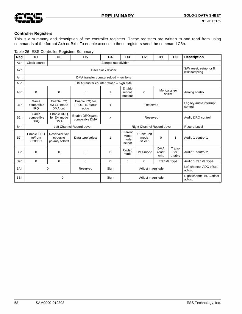
58 SAM0090-012398 ESS Technology, Inc.
SOLO-1 DATA SHEET
REGISTERSPRELIMINARY
Controller Re gistersThis is a summary and description of the controller registers. These registers are written to and read from usingcommands of the format Axh or Bxh. To enable access to these registers send the command C6h.
Table 26 ESS Controller Registers SummaryReg D7 D6 D5 D4 D3 D2 D1 D0 Description
A1h Clock source Sample rate divider
A2h Filter clock divider S/W reset, setup for 8 kHz sampling
A4h DMA transfer counter reload – low byte
A5h DMA transfer counter reload – high byte
A8h 0 0 0 1Enable record monitor
0 Mono/stereo select Analog control
B1hGame
compatible IRQ
Enable IRQ ovf Ext mode
DMA cntr
Enable IRQ for FIFO1 HE status
edgex Reserved Legacy audio interrupt
control
B2hGame
compatible DRQ
Enable DRQ for Ext mode
DMA
Enable DRQ game compatible DMA x Reserved Audio DRQ control
B4h Left Channel Record Level Right Channel Record Level Record Level
B7hEnable FIFO
to/from CODEC
Reserved. Set opposite
polarity of bit 3Data type select 1
Stereo/Mono mode select
16-bit/8-bit mode select
0 1 Audio 1 control 1
B8h 0 0 0 0 Codec mode DMA mode
DMA read/write
Trans-fer
enableAudio 1 control 2
B9h 0 0 0 0 0 0 Transfer type Audio 1 transfer type
BAh 0 Reserved Sign Adjust magnitude Left channel ADC offset adjust
BBh 0 Sign Adjust magnitude Right channel ADC offset adjust
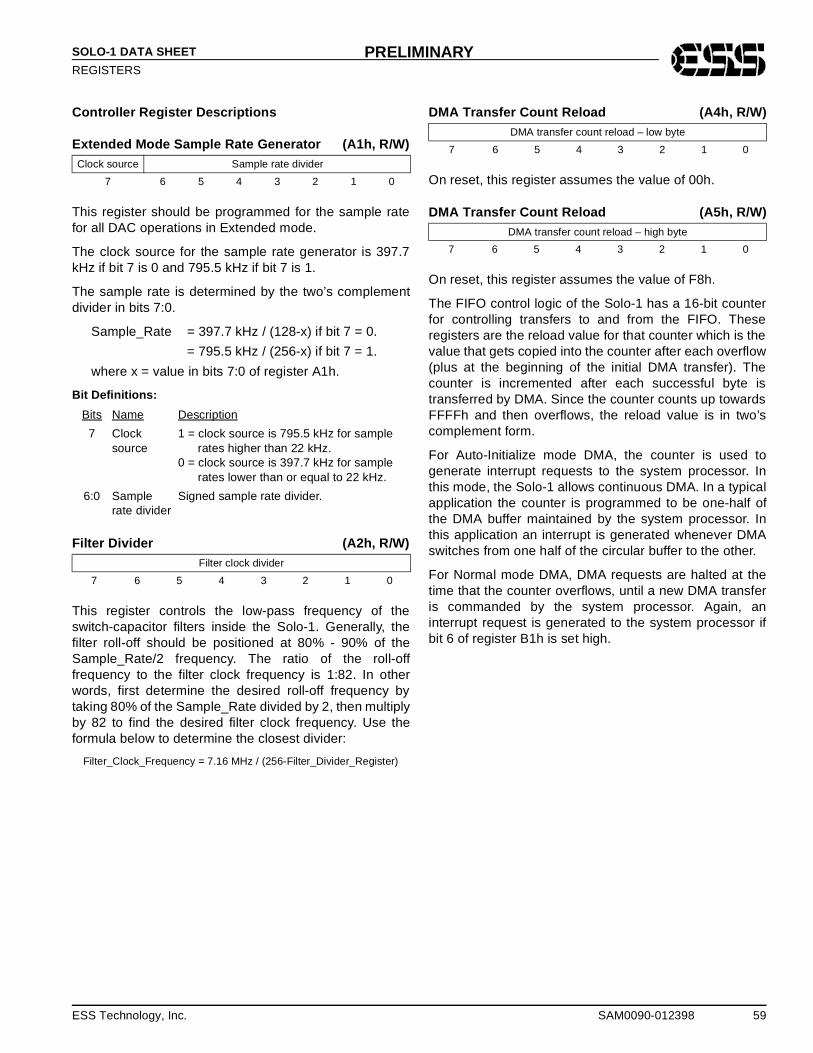
ESS Technology, Inc. SAM0090-012398 59
SOLO-1 DATA SHEET
REGISTERSPRELIMINARY
Controller Re gister Descriptions
Extended Mode Sample Rate Generator (A1h, R/W)
This register should be programmed for the sample ratefor all DAC operations in Extended mode.
The clock source for the sample rate generator is 397.7kHz if bit 7 is 0 and 795.5 kHz if bit 7 is 1.
The sample rate is determined by the two’s complementdivider in bits 7:0.
Sample_Rate = 397.7 kHz / (128-x) if bit 7 = 0.
= 795.5 kHz / (256-x) if bit 7 = 1.
where x = value in bits 7:0 of register A1h.
Bit Definitions:
Filter Divider (A2h, R/W)
This register controls the low-pass frequency of theswitch-capacitor filters inside the Solo-1. Generally, thefilter roll-off should be positioned at 80% - 90% of theSample_Rate/2 frequency. The ratio of the roll-offfrequency to the filter clock frequency is 1:82. In otherwords, first determine the desired roll-off frequency bytaking 80% of the Sample_Rate divided by 2, then multiplyby 82 to find the desired filter clock frequency. Use theformula below to determine the closest divider:
Filter_Clock_Frequency = 7.16 MHz / (256-Filter_Divider_Register)
DMA Transfer Count Reload (A4h, R/W)
On reset, this register assumes the value of 00h.
DMA Transfer Count Reload (A5h, R/W)
On reset, this register assumes the value of F8h.
The FIFO control logic of the Solo-1 has a 16-bit counterfor controlling transfers to and from the FIFO. Theseregisters are the reload value for that counter which is thevalue that gets copied into the counter after each overflow(plus at the beginning of the initial DMA transfer). Thecounter is incremented after each successful byte istransferred by DMA. Since the counter counts up towardsFFFFh and then overflows, the reload value is in two’scomplement form.
For Auto-Initialize mode DMA, the counter is used togenerate interrupt requests to the system processor. Inthis mode, the Solo-1 allows continuous DMA. In a typicalapplication the counter is programmed to be one-half ofthe DMA buffer maintained by the system processor. Inthis application an interrupt is generated whenever DMAswitches from one half of the circular buffer to the other.
For Normal mode DMA, DMA requests are halted at thetime that the counter overflows, until a new DMA transferis commanded by the system processor. Again, aninterrupt request is generated to the system processor ifbit 6 of register B1h is set high.
Clock source Sample rate divider
7 6 5 4 3 2 1 0
Bits Name Description
7 Clock source
1 = clock source is 795.5 kHz for sample rates higher than 22 kHz.0 = clock source is 397.7 kHz for sample rates lower than or equal to 22 kHz.
6:0 Sample rate divider
Signed sample rate divider.
Filter clock divider
7 6 5 4 3 2 1 0
DMA transfer count reload – low byte
7 6 5 4 3 2 1 0
DMA transfer count reload – high byte
7 6 5 4 3 2 1 0

60 SAM0090-012398 ESS Technology, Inc.
SOLO-1 DATA SHEET
REGISTERSPRELIMINARY
Analo g Control (A8h, R/W)
When programming the FIFO for DMA playback modifyonly bits 1:0. When programming the FIFO for DMA recordmodify only bits 3, 1, and 0. Read this register first topreserve the remaining bits.
Bit Definitions:
Legacy Audio Interrupt Control (B1h, R/W)
Bit Definitions:
DRQ Control (B2h, R/W)
Bit Definitions:
0 0 0 1 Record monitor enable 0 Stereo/mono
select
7 6 5 4 3 2 1 0
Bits Name Description
7:5 0 Reserved. Always write 0.
4 1 Reserved. Always write 1.
3 Record monitor enable
1 = Enable record monitor.0 = Disable record monitor.
2 0 Reserved. Always write 0.
1:0 Stereo/mono select
Select operation mode of first DMA converters.Bit 1 Bit 0 Mode 0 0 Reserved 0 1 Stereo 1 0 Mono 1 1 Reserved
Game compatible
IRQ
Enable IRQ ovf Ext mode DMA cntr
Enable IRQ for FIFO1 HE status
edgex Reserved
7 6 5 4 3 2 1 0
Bits Name Description
7 Game com-patible IRQ
Reserved for Compatibility mode. Leave zero for Extended mode.
6 Enable IRQ ovf Ext mode DMA cntr
Set high to receive interrupts for each over-flow of the Solo-1 DMA counter in Extended mode.
5 Enable IRQ for FIFO1 HE status edge
Set high to receive interrupts for FIFO Half-Empty transitions when doing block I/O to/from the FIFO in Extended mode.
4 – No function. The audio device activate bit serves the purpose of enabling the interrupt pin.
3:0 – Reserved.
Game compatible
DRQ
Enable DRQ for Extended mode
DMA
Enable DRQ game compatible
DMAx Reserved
7 6 5 4 3 2 1 0
Bits Name Description
7 Game compatible DRQ
Reserved for Compatibility mode. Leave zero for Extended mode.
6 Enable DRQ for Extended mode DMA
1 = Enable DRQ outputs and DACKB inputs for DMA transfers in Extended mode.0 = Enable block I/O to/from the FIFO in Extended mode.
5 Enable DRQ gamecompatible DMA
Reserved for Compatibility mode. Leave zero for Extended mode.
4 – No function. The DRQ lines always drive (there is no enable). If neither bit 5 nor bit 6 are set high, the first audio DRQ is always low.
3:0 – Reserved.

ESS Technology, Inc. SAM0090-012398 61
SOLO-1 DATA SHEET
REGISTERSPRELIMINARY
Record Level (B4h, R/W)
Register B4h allows for independent left and right recordlevel. Each channel has 16 levels (excluding mute). Theamount of gain or attenuation for each level is different formicrophone than for all other sources. The record levelsare listed in the following table.
Audio 1 Control 1 (B7h, R/W)
Bit Definitions:
Audio 1 Control 2 (B8h, R/W)
Bit Definitions:
Left channel record level Right channel record level
7 6 5 4 3 2 1 0
Record Level Gain for MicGain for Other
Sources
0 +0 dB -6.0 dB
1 +1.5 dB -4.5 dB
2 +3.0 dB -3.0 dB
3 +4.5 dB -1.5 dB
4 +6.0 dB 0 dB
5 +7.5 dB +1.5 dB
6 +9.0 dB +3.0 dB
7 +10.5 dB +4.5 dB
8 +12.0 dB +6.0 dB
9 +13.5 dB +7.5 dB
10 +15.0 dB +9.0 dB
11 +16.5 dB +10.5 dB
12 +18.0 dB +12.0 dB
13 +19.5 dB +13.5 dB
14 +21.0 dB +15.0 dB
15 +22.5 dB +16.5 dB
Enable FIFO to/from CODEC
Set oppo-site bit
3
FIFO signed mode
1FIFO stereo mode
FIFO 16-bit mode
0 Generate load signal
7 6 5 4 3 2 1 0
Bits Name Description
7 Enable FIFO to/from CODEC
1 = Enable first DMA FIFO connection to DAC or ADC. This allows transfers to/from the FIFO and the analog circuitry.0 = Disable first DMA FIFO connection to DAC or ADC.
6 Set opposite bit 3
Reserved function. This bit must be set to the opposite polarity of bit 3: high for mono and low for stereo.
5 FIFO signed mode
1 = First DMA FIFO two’s complement mode (signed data).0 = First DMA FIFO unsigned (offset 8000).
4 1 Reserved. Always write 1.
3 FIFO stereo mode
1 = First DMA FIFO stereo mode.0 = First DMA FIFO mono mode.Bit 6 must be set at the opposite polarity of this bit: high for mono, low for stereo.
2 FIFO 16-bit mode
1 = First DMA FIFO 16-bit mode.0 = First DMA FIFO 8-bit mode.
1 0 Reserved. Always write 0.
0 Generate load signal
Write 1. Generates a load signal that copies DAC Direct Access Holding register to DAC on the next sample rate clock edge (sample rate is determined by Extended mode regis-ter A1h). This bit is cleared after the holding register is copied to the DAC.
0 0 0 0 CODEC mode
DMA mode
DMA read enable
DMA transfer enable
7 6 5 4 3 2 1 0
Bits Name Description
7:4 0 Reserved. Always write 0.
3 CODEC mode
1 = first DMA converters in ADC mode.0 = first DMA converters in DAC mode.
2 DMA mode 1 = auto-initialize mode.0 = normal DMA mode.
1 DMA read enable
1 = first DMA is read (e.g. for ADC operation).0 = first DMA is write (e.g. for DAC operation).
0 DMAtransfer enable
First DMA active-low reset. When high, first DMA is allowed to proceed.

62 SAM0090-012398 ESS Technology, Inc.
SOLO-1 DATA SHEET
REGISTERSPRELIMINARY
Audio 1 Transfer T ype (B9h, R/W)
Bit Definitions:
Left Channel ADC Offset Ad just (BAh, R/W)
This register is reset to zero by hardware reset and isunaffected by software reset.
Bit Definitions:
Right Channel ADC Offset Ad just (BBh, R/W)
This register is reset to zero by hardware reset and isunaffected by software reset.
Bit Definitions:
Bits 4 (sign) and 3:0 (adjust magnitude) of the ADC OffsetAdjust registers cause a constant value to be added to theADC converter output, as shown in the following:
Formula:
bit 4 = 0: offset = 64 * bits[3:0]
bit 4 = 1: offset = -64 * (bits[3:0] +1)
To calculate the offset adjust code, first measure the ADCoffset for both right and left channels before adjustment byfollowing these steps:
1. Program Extended mode registers BAh and BBh bits 4:0 to be zero (no digital offset).
2. Select a zero-amplitude (or low amplitude) recording source.
3. Set the recording volume to minimum by setting Extended mode register B4h to zero.
4. Make a stereo 16-bit two’s complement recording at 11 kHz sample rate of 2048 stereo samples (2048 stereo samples = 4096 words = 8192 bytes, which is about 190 milliseconds).
5. Use the last 1024 stereo samples to calculate a long term average for both left and right channels.
6. With this average DC offset, calculate the best digital offset to bring the sum closest to zero, using the codes and offsets listed in the table above.
0 0 0 0 0 0 DMA transfer type select
7 6 5 4 3 2 1 0
Bits Name Description
7:2 0 Reserved. Always write 0.
1:0 DMA transfer type select
Selects the DMA transfer type for the first DMA:Bit 1 Bit 0 Transfer Type Bytes/DMA Request 0 0 Single – 0 1 Demand 2 1 0 Demand 4 1 1 Reserved –
0 0 Disable time delay on analog wake-up Sign Adjust magnitude
7 6 5 4 3 2 1 0
Bits Name Description
7:6 0 Reserved. Always write 0.
5 Disable time delay on analog wake-up
Normally, the AOUT_L and AOUT_R pins are muted for 100 msec ± 20 msecs after hardware reset or after the analog sub-systems wake from power-down. Set high to disable delay.This bit is cleared by hardware reset.
4:0 Sign/Adjust magnitude
See the explanation for bits 4:0 following register BBh.
0 0 0 Sign Adjust magnitude
7 6 5 4 3 2 1 0
Bits Name Description
7:5 0 Reserved. Always write 0.
4:0 Sign/Adjust magnitude
See the following explanation for bits 4:0.
Code Offset Code Offset
00h 0 10h -64
01h +64 11h -128
02h +128 12h -192
03h +192 13h -256
04h +256 14h -320
05h +320 15h -384
06h +384 16h -448
07h +448 17h -512
08h +512 18h -576
09h +576 19h -640
0Ah +640 1Ah -704
0Bh +704 1Bh -768
0Ch +768 1Ch -832
0Dh +832 1Dh -896
0Eh +896 1Eh -960
0Fh +960 1Fh -1024
ESS Technology, Inc. SAM0090-012398 63
SOLO-1 DATA SHEET
AUDIO MICROCONTROLLER COMMAND SUMMARYPRELIMINARY
AUDIO MICROCONTROLLER COMMAND SUMMARY
Table 27 Command Summary
CommandData Byte(s) Write/Read
Function
10h 1 write Direct write 8-bit DAC. Data is 8-bit unsigned format.
11h 2 writes Direct write 16-bit DAC. Data is 16-bit unsigned format, first low byte then high byte.
14h 2 writes Start Normal mode DMA for 8-bit DAC transfer. Data is transfer count - 1, least byte first. Stereo DAC transfer if stereo flag is set in mixer register 0Eh. Maximum sample rate is 44 kHz mono, 22 kHz ste-reo.
15h 2 writes Start Normal mode DMA for 16-bit DAC transfer. Data is transfer count - 1, least byte first. Stereo DAC transfer if stereo flag is set in mixer register 0EH. Maximum sample rate is 22 kHz mono, 11 kHz stereo.
1Ch Start Auto-Initialize mode DMA for 8-bit DAC transfer. Block size must be previously set by command 48h. Stereo DAC transfer if stereo flag is set in mixer register 0Eh. Maximum sample rate is 44 kHz mono, 22 kHz stereo.
1Dh Start Auto-Initialize mode DMA for 16-bit DAC transfer. Block size must be previously set by com-mand 48h. Stereo DAC transfer if stereo flag is set in mixer register 0Eh. Maximum sample rate is 22 kHz mono, 11 kHz stereo.
20h 1 read Direct mode 8-bit ADC. Data is 8-bit unsigned. Firmware controlled input volume for AGC.
21h 2 reads Direct mode 16-bit ADC, returns least byte first. Data is 16-bit unsigned format. Input volume con-trolled by command DDh.
24h 2 writes Start Normal mode DMA for 8-bit ADC transfer. Data is transfer count - 1, least byte first. Firmware controlled input volume for AGC. Maximum sample rate is 22 kHz: use command 99h for higher rates up to 44 kHz.
25h 2 writes Start Normal mode DMA for 16-bit ADC transfer. Data is transfer count - 1, least byte first. Input vol-ume controlled via command DDh. Maximum sample rate is 22 kHz.
2Ch Start Auto-Initialize mode DMA for 8 bit ADC transfer. Block size must be previously set by command 48h. Firmware controlled input volume for AGC. Maximum sample rate is 22 kHz: use command 98h for higher rates up to 44 kHz.
2Dh Start Auto-Initialize mode DMA for 16-bit ADC transfer. Block size must be previously set by com-mand 48h. Input volume is controlled by command DDh. Maximum sample rate is 22 kHz.
30h/31h MIDI input mode. Detects MIDI serial input data and transfers to data register, setting Data-Available flag in register SBBase+Eh. Command 31h will also generate an interrupt request for each byte received.Exit MIDI input mode by executing a write to port SBBase+Ch. The data written is ignored. A soft-ware reset will also exit this mode.
34h/35h MIDI UART mode. Acts like commands 30h/31h, except that any data written to SBBase+Ch will be transmitted as MIDI serial output data. The only way to exit this mode is through software reset.
38h 1 write MIDI output. Transmit one byte.
40h 1 write Set time constant, X, for timer used for DMA mode DAC/ADC transfers: rate = 1 MHz / (256-X) X must be less than or equal to 233. For stereo DAC, program sample rate for twice the per-channel rate.
41h 1 write Alternate set time constant, X: rate = 1.5 MHz / (256-X)This command provides more accurate timing for certain rates such as 22,050. X must be less than equal to 222. For stereo DAC, program sample rate for twice the per-channel rate.
42h 1 write Set filter clock independently of timer rate. (note that the filter clock is automatically set by commands 40h/41h) Filter clock rate: rate = 7.16E6 / (256-X)The relationship between the low-pass filter -3 dB point and the filter clock rate is approximately 1:82.
48h 2 writes Set block size-1 for high speed mode and auto-init mode transfer, least byte first.
64h 2 writes Start ESPCM® 4.3-bit (low compression) format DMA transfer to DAC. Data is transfer count - 1, least byte first.
64 SAM0090-012398 ESS Technology, Inc.
SOLO-1 DATA SHEET
AUDIO MICROCONTROLLER COMMAND SUMMARYPRELIMINARY
65h 2 writes Same as command 64h, except with reference byte flag.
66h 2 writes Start ESPCM® 3.4-bit (medium compression) format DMA transfer to DAC. Data is transfer count - 1, least byte first.
67h 2 writes Same as command 66h, except with reference byte flag.
6Ah 2 writes Start ESPCM® 2.5-bit (high compression) format DMA transfer to DAC. Data is transfer count - 1, least byte first.
6Bh 2 writes Same as command 6Ah, except with reference byte flag.
6Eh 2 writes Start ESPCM® 4.3-bit (low compression) format ADC, compression, and DMA transfer. Data is transfer count - 1, least byte first.
6Fh 2 writes Same as command 6Eh, except with reference byte flag.
74h 2 writes Start ADPCM 4-bit format DMA transfer to DAC. Data is transfer count - 1, least byte first.
75h 2 writes Same as command 74h, except with reference byte flag.
76h 2 writes Start ADPCM 2.6-bit format DMA transfer to DAC. Data is transfer count - 1, least byte first.
77h 2 writes Same as command 76h, except with reference byte flag.
7Ah 2 writes Start ADPCM 2-bit format DMA transfer to DAC. Data is transfer count - 1, least byte first.
7Bh 2 writes Same as command 7Ah, except with reference byte flag.
80h 2 writes Generate silence period. Data is number of samples - 1.
90h Start Auto-Initialize DMA 8-bit transfer to DAC. Transfer count must be previously set by command 48h.
91h Start DMA 8-bit transfer to DAC. Transfer count must be previously set by command 48h.
98h Start High-Speed mode, Auto-Initialize, DMA 8-bit transfer from ADC. Transfer count must be previ-ously set by command 48h. There is no AGC. Input volume is controlled with command DDh. Maxi-mum sample rate is 44 kHz.
99h Start High-Speed mode, DMA 8-bit transfer from ADC. Transfer count must be previously set by com-mand 48h. There is no AGC. Input volume is controlled with command DDh. Maximum sample rate is 44 kHz.
Axh, Bxh, Cxh
(where x = 0 to Fh) Solo-1 extension commands. Many of these commands are used to access the Solo-1’s controller registers. For information on these registers, see the register descriptions.
C0h 1 write,1 read Read controller registers A0h to BFh. Write this command followed by the register number, then read register contents from SBBase+Ah.
C1h Resume after suspend.
C6h Enable Solo-1 Extension commands Axh, Bxh. Must be issued after every reset.
C7h Disable Solo-1 Extension commands Axh, Bxh.
D0h Pause DMA. Internal FIFO operations continue until the FIFO is empty (DAC transfer) or full (ADC transfer). It is not necessary to use this command to stop DMA if the transfer is completed normally and the end-of-DMA interrupt is generated.
D1h Enable Audio 1 DAC input to mixer.
D3h Disable Audio 1 DAC input to mixer.
D4h Continue DMA after command D0h.
D8h 1 read Return Audio 1 DAC enable status: 0=disabled; FFh=enabled
DCh 1 read Return current input gain, 0-15, (valid during 16-bit ADC and 8-bit “high speed mode” ADC).
DDh 1 write Write current input gain, 0-15, (valid during 16-bit ADC and 8-bit “high speed mode” ADC).
E1h 2 reads Return version number high (3), followed by version number low (1). This indicates Sound Blaster Pro compatibility.
Table 27 Command Summary (Continued)
CommandData Byte(s) Write/Read
Function
ESS Technology, Inc. SAM0090-012398 65
SOLO-1 DATA SHEET
POWER MANAGEMENTPRELIMINARY
POWER MANAGEMENT
The Solo-1 is a high-performance device with low powerconsumption. In addition to the low-power deep sub-micron CMOS mixed-signal technology used to processthe Solo-1, various features are designed into the deviceto provide benefits from popular power-saving techniques.
CLKRUN Protocol
The PCI CLKRUN feature is one of the primary methodsof power management on the PCI bus interface of theSolo-1 for the notebook computer. The protocol is definedin the “PCI Mobile Design Guide”, published by the PCISpecial Interest Group (PCISIG). To use this feature, aPCI sideband signal, CLKRUN, must be supported by thechipset. All PCI bus signals must be in leakage controlstate to shut down leak current at IO buffers, as specifiedin the “PCI Mobile Design Guide.”
PCI Power Management Interface (PPMI)
The “PCI Bus Power Management Interface (PPMI)Specification,” also published by the PCISIG, establishesthe infrastructure required to let the operating systemcontrol the power of PCI functions. This is done by definingstandard PCI interface and operations to manage thepower of PCI functions on the bus. PCI functions can beassigned one of five power management states, and thePCI bus itself can be assigned one of four powermanagement states.
The Solo-1 (as a PCI function) supports the following fivepower-management states:
• D0 – full power
• D1 – embedded DSP is halted
• D2 – D1 and analog functions are off
• D3hot – D2 and oscillator are off
• D3cold – power supply is off
To minimize the power consumed by the Solo-1 in D3hot
state, the PCI bus should be in B2 or B3 state, where thePCI clock is stopped.
All PPMI registers are located in the PCI configurationspace. This allows the operating system to identify thepower management capabilities of the Solo-1 without aspecial driver.
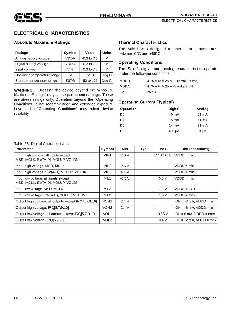
66 SAM0090-012398 ESS Technology, Inc.
SOLO-1 DATA SHEET
ELECTRICAL CHARACTERISTICSPRELIMINARY
ELECTRICAL CHARACTERISTICS
Absolute Maximum Ratings
WARNING: Stressing the device beyond the “AbsoluteMaximum Ratings” may cause permanent damage. Theseare stress ratings only. Operation beyond the “OperatingConditions” is not recommended and extended exposurebeyond the “Operating Conditions” may affect devicereliability.
Thermal Characteristics
The Solo-1 was designed to operate at temperaturesbetween 0°C and +85°C.
Operating Conditions
The Solo-1 digital and analog characteristics operateunder the following conditions:
Operating Current (Typical)
Ratings Symbol Value Units
Analog supply voltage VDDA -0.3 to 7.0 V
Digital supply voltage VDDD -0.3 to 7.0 V
Input voltage VIN -0.3 to 7.0 V
Operating temperature range TA 0 to 70 Deg C
Storage temperature range TSTG -50 to 125 Deg C VDDD 4.75 V to 5.25 V (5 volts ± 5%)
VDDA 4.75 V to 5.25 V (5 volts ± 5%)
TA 25 °C
Operation Digital Analog
D0 40 mA 61 mA
D1 15 mA 61 mA
D2 14 mA 61 mA
D3 400 µA 8 µA
Table 28 Digital CharacteristicsParameter Symbol Min Typ Max Unit (conditions)
Input high voltage: all inputs exceptMSD, MCLK, SW(A-D), VOLUP, VOLDN
VIH1 2.0 V VDDD+0.5 VDDD = min
Input high voltage: MSD, MCLK VIH2 2.6 V VDDD = min
Input high voltage: SW(A-D), VOLUP, VOLDN VIH3 4.1 V VDDD = min
Input low voltage: all inputs exceptMSD, MCLK, SW(A-D), VOLUP, VOLDN
VIL1 -0.5 V 0.8 V VDDD = max
Input low voltage: MSD, MCLK VIL2 1.2 V VDDD = max
Input low voltage: SW(A-D), VOLUP, VOLDN VIL3 1.3 V VDDD = max
Output high voltage: all outputs except IRQ[5,7,9,10] VOH1 2.4 V IOH = -3 mA, VDDD = min
Output high voltage: IRQ[5,7,9,10] VOH2 2.4 V IOH = -8 mA, VDDD = min
Output low voltage: all outputs except IRQ[5,7,9,10] VOL1 0.55 V IOL = 6 mA, VDDD = max
Output low voltage: IRQ[5,7,9,10] VOL2 0.4 V IOL = 12 mA, VDDD = max
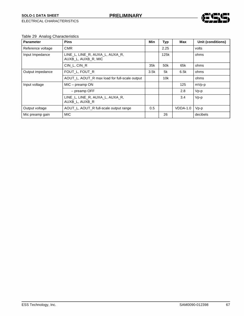
ESS Technology, Inc. SAM0090-012398 67
SOLO-1 DATA SHEET
ELECTRICAL CHARACTERISTICSPRELIMINARY
Table 29 Analog CharacteristicsParameter Pins Min Typ Max Unit (conditions)
Reference voltage CMR 2.25 volts
Input Impedance LINE_L, LINE_R, AUXA_L, AUXA_R,AUXB_L, AUXB_R, MIC
125k ohms
CIN_L, CIN_R 35k 50k 65k ohms
Output impedance FOUT_L, FOUT_R 3.5k 5k 6.5k ohms
AOUT_L, AOUT_R max load for full-scale output 10k ohms
Input voltage MIC – preamp ON 125 mVp-p
– preamp OFF 2.8 Vp-p
LINE_L, LINE_R, AUXA_L, AUXA_R, AUXB_L, AUXB_R
3.4 Vp-p
Output voltage AOUT_L, AOUT_R full-scale output range 0.5 VDDA-1.0 Vp-p
Mic preamp gain MIC 26 decibels
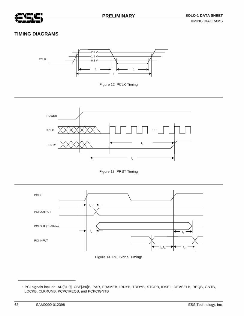
68 SAM0090-012398 ESS Technology, Inc.
SOLO-1 DATA SHEET
TIMING DIAGRAMSPRELIMINARY
TIMING DIAGRAMS
Figure 12 PCLK Timing
Figure 13 PRST Timing
Figure 14 PCI Signal Timing1
PCLK
t2
1.5 V
0.8 V
2.0 V
t3
t1
PCLK
t5
t4
POWER
PRST#
1. PCI signals include: AD[31:0], CBE[3:0]B, PAR, FRAMEB, IRDYB, TRDYB, STOPB, IDSEL, DEVSELB, REQB, GNTB,LOCKB, CLKRUNB, PCPCIREQB, and PCPCIGNTB
PCI OUTPUT
PCLK
PCI OUT (Tri-State)
PCI INPUT
t6, t7
t8 t9
t10, t11 t12

ESS Technology, Inc. SAM0090-012398 69
SOLO-1 DATA SHEET
TIMING CHARACTERISTICSPRELIMINARY
TIMING CHARACTERISTICS
Table 30 Timing Characteristics
Symbol Parameter Min Typ Max Units
t1 PCLK cycle time 30 inf. ns
t2 PCLK high time 11 ns
t3 PCLK low time 11 ns
– PCLK slew rate 1 4 V/ns
t4 PRST# active time after power stable 1 ms
t5 PRST# active time after PCLK stable 1000 t1
t6 PCLK to signal valid delay (except REQB) 2 TBD ns
t7 PCLK to signal valid delay (REQB) ns
t8 Float to active delay 2 ns
t9 Active to float delay 28 ns
t10 Input setup time to PCLK (except IDSEL, GNTB) 7 ns
t11 Input setup time to PCLK (IDSEL, GNTB) 12 ns
t12 Input hold time from PCLK 0 ns

70 SAM0090-012398 ESS Technology, Inc.
SOLO-1 DATA SHEET
MECHANICAL DIMENSIONSPRELIMINARY
MECHANICAL DIMENSIONS
Figure 15 Solo-1 Mechanical Dimensions
Symbol DescriptionMillimeters
Min Nom MaxD Lead to lead, X-axis 15.75 16.00 16.25
D1 Package’s outside, X-axis 13.90 14.00 14.10
E Lead to lead, Y-axis 15.75 16.00 16.25
E1 Package’s outside, Y-axis 13.90 14.00 14.10
A1 Board standoff 0.05 0.10 0.15
A2 Package thickness 1.35 1.40 1.45
b Lead width 0.17 0.22 0.27
e Lead pitch - 0.50 -
e1 Lead gap 0.24 - -
L Foot length 0.45 0.60 0.75
L1 Lead length 0.93 1.00 1.07
- Foot angle 0° 7°
- Coplanarity - - 0.102
- Leads in X-axis - 25 -
- Leads in Y-axis - 25 -
- Total leads - 100 -
- Package type - TQFP -
E1
A2 A1
L
E
D1
b
D
Solo-1e
1
e1
L1100-Pin TQFP

ESS Technology, Inc. SAM0090-012398 71
SOLO-1 DATA SHEET
APPENDIX A: ES689/ES69X DIGITAL SERIAL INTERFACEPRELIMINARY
APPENDIX A: ES689/ES69x DIGITAL SERIAL INTERFACE
In order for the ES689/ES69x to acquire the FM DAC, bit4 of mixer register 48h inside the Solo-1 must be set high.When bit 4 is set high, activity on the MCLK signal causesthe Solo-1 to connect the FM DAC to the ES689/ES69x. IfMCLK stays low for more than a few sample periods, theSolo-1 reconnects the FM DAC to the FM synthesizer.
After reset, the ES689/ES69x transmits samplescontinuously. In this mode, bit 4 of mixer register 48h mustbe set/cleared to assign the current owner of the FM DAC.
The ES689/ES69x can be programmed to enter Activity-Detect mode using system exclusive command 4. Formore information on system exclusive commands, see theappropriate ES689/ES69x Data Sheet. In this mode, theES689/ES69x blocks the serial port output (i.e., sets MSDand MCLK low) if no MIDI input is detected on the MSI pinfor a period of 5 seconds. It resumes output of data on theserial port as soon as a MIDI input is detected on the MSIpin. This is the recommended mode of operation.
Bit Clock Rate (MCLK): 2.75 MHz
Sample Rate: 42,968.75 Hz
MCLK Clocks per Sample: 33 clocks (+ 31 missing clocks)
MSD Format: 16 bits, unsigned (offset 8000h), MSB first
MSD changes after rising edge of MCLK. Hold time relative to MCLK rising edge is 0-25 nanoseconds.
00 01 02 14 15 16 17 29 30 31 32 33 62 63 00
L15 L14 L13 L1 L0 R15 R14 R2 R1 R0MSD
MCLK
MSB MSB
Right DataLeft Data
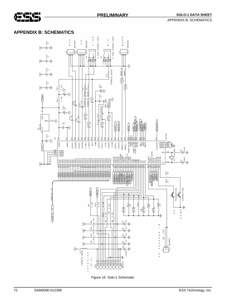
72 SAM0090-012398 ESS Technology, Inc.
SOLO-1 DATA SHEET
APPENDIX B: SCHEMATICSPRELIMINARY
APPENDIX B: SCHEMATICS
Figure 16 Solo-1 Schematic
C3
5.
1
VC
C
C2
1.
1C
22
.1
VC
CV
CC
VC
C
C2
0.
1
VD
DA
IN
3O
UT
1
G N D 2
U1
78
L0
5
C2
3.
1
+1
2V
VC
C
HD
A[
31
..
0]
HA
D[
31
..
0]
AD
0
16
AD
1
15
AD
2
14
AD
3
13
AD
4
12
AD
5
11
AD
6
10
AD
7
9
AD
9
6
AD
10
5
AD
11
4
AD
12
3
AD
13
2
AD
14
9
9
AD
15
9
8
AD
16
8
8
AD
17
8
7
AD
18
8
6
AD
19
8
5
AD
20
8
4
AD
22
8
2
AD
24
7
6
AD
26
7
4
AD
28
7
2
AD
29
7
1
AD
30
7
0
AD
31
6
9
CB
E0
B
8
CB
E1
B
97
CB
E2
B
89
CB
E3
B
77
FR
AM
EB
9
0
IRD
YB
9
1
V D D D1 7 V D D D6 4 V D D D8 0
G N D D 2 4G N D D 5 2G N D D 8 1
SW
A
34
SW
B
33
SW
C
32
SW
D
31
TA
3
0
TB
2
9
TC
2
8
TD
2
7
VD
DA
43
GN
DA
41
AU
XB
L3
5
AU
XB
R3
6
AU
XA
L3
7
AU
XA
R3
8
LIN
EL
48
LIN
ER
49
MIC
40
CM
R3
9
CA
P3
D4
2
FO
UT
L4
5
CIN
L4
6
FO
UT
R4
4
CIN
R4
7
AO
UT
L5
0
AO
UT
R5
1
X I 1 9
X O 1 8
VO
LD
N
20
VO
LU
P
21
PR
ST
B
65
PC
LK
6
6
MO
NO
_I
26
IRQ
A/I
NT
AB
60
59
58
MC
LK
22
MS
D2
3M
SO
55
MS
I5
6
AD
23
7
9
AD
21
8
3
DE
VS
EL
B
93
ST
OP
B
94
LO
CK
B
95
MO
NO
_O
25
IRQ
D/
SIR
Q5
7
PC
SP
KI
5
4
GN
TB
6
7
PC
SK
PO
53
G N D D 1 0 0
V D D D1
AD
8
7
AD
25
7
5
AD
27
7
3
PC
PC
IRE
QB
61
TR
DY
B
92
PA
R
96
CL
KR
UN
B
63
RE
QB
68
PC
PC
IGN
TB
6
2ID
SE
L
78
U2
SO
LO
1
HD
A0
HD
A1
HD
A2
HD
A3
HD
A4
HD
A5
HD
A6
HD
A7
HD
A8
HD
A9
C9
.1
C3
3.
22
C1
01
0
R1
0
7.
5K
R1
1
7.
5K
C1
11
0
C3
4.
22
AU
X1 2 3J
6
3x
1
HE
AD
ER
LI
NE
CD
1 2 3 4J2
4x
1
HE
AD
ER
1
2
3
4
5J
4
3.
5m
m
ST
ER
EO
J
AC
K
C1
2.
1
C3
0.
22
L2
FE
RR
ITE
B
EA
DL
3F
ER
RIT
E
BE
AD
C3
1 .2
2
C2
9.
22
C3
2 .2
2
HD
A1
0H
DA
11
HD
A1
2H
DA
13
HD
A1
4H
DA
15
HD
A1
6H
DA
17
HD
A1
8H
DA
19
HD
A2
0H
DA
21
R6
2.
2K
MS
INR
32
.2
KR
42
.2
KR
52
.2
K
VC
CV
CC
VC
CV
CC
JO
YS
TI
CK
/M
ID
I
L1
FE
RR
ITE
B
EA
D
R2
2.
2K
VC
C
8
15
7
14
6
13
5
12
4
11
3
10
2
9
1
J1
DB
15
S
R1
2.
2K
R8
2.
2KR7
2.
2K
R2
0
2.
2K
HC
BE
0n
MS
OU
T
R1
52
.2
K
HD
A2
2H
DA
23
HD
A2
4H
DA
25
HD
A2
6H
DA
27
HD
A2
8H
DA
29
HD
A3
0H
DA
31
C1
3.
04
7
C1
6.
22
C1
7.
22
C1
4.
1C
15
47
C2
76
80
pF
C2
86
80
pF
L4
FE
RR
I TE
B
EA
D
1
2
3
4
5
J5
3.
5m
m
ST
ER
EO
J
AC
K
MI
C
MO
NO
1 2 3J7
3x
1
HE
AD
ER
C1
8
.2
2C
19
.2
2M
ON
O_
I
MO
NO
_O
AO
UT
L
AO
UT
R
INT
An
HP
AR
C2
4.
01
C2
5.
01
R1
21
M
HC
BE
1n
HC
BE
2n
HC
BE
3n
HF
RA
ME
nH
IR
DY
nH
TR
DY
nH
DE
VS
EL
nH
ST
OP
nH
LO
CK
n
CL
KR
UN
n
C3
.0
1
C4
.0
1
C5
.0
1
C1
15
0p
F
C2
.0
1
C6
.0
1
R1
3
1M C
26
.0
1 R1
41
MP
CP
CI
GN
Tn
HID
SE
L
MS
DM
CL
K
MS
O6
92
MS
OU
T
PC
PC
IRE
Qn
HR
EQ
n
SIR
Q_
PC
SP
KO
Y1
14
.3
18
M
Hz
R1
71
K
HG
NT
nH
CL
KH
RS
Tn
R1
61
K
S1
PU
SH
BU
TT
ON
R1
91
M
R9
10
K
PC
S
PE
AK
ER
I
N
1 2
J3
2x
1
HE
AD
ER
UP
DO
WN
S2
PU
SH
BU
TT
ON
C7
10
pF
C8
10
pF
IRQ
BIR
QC
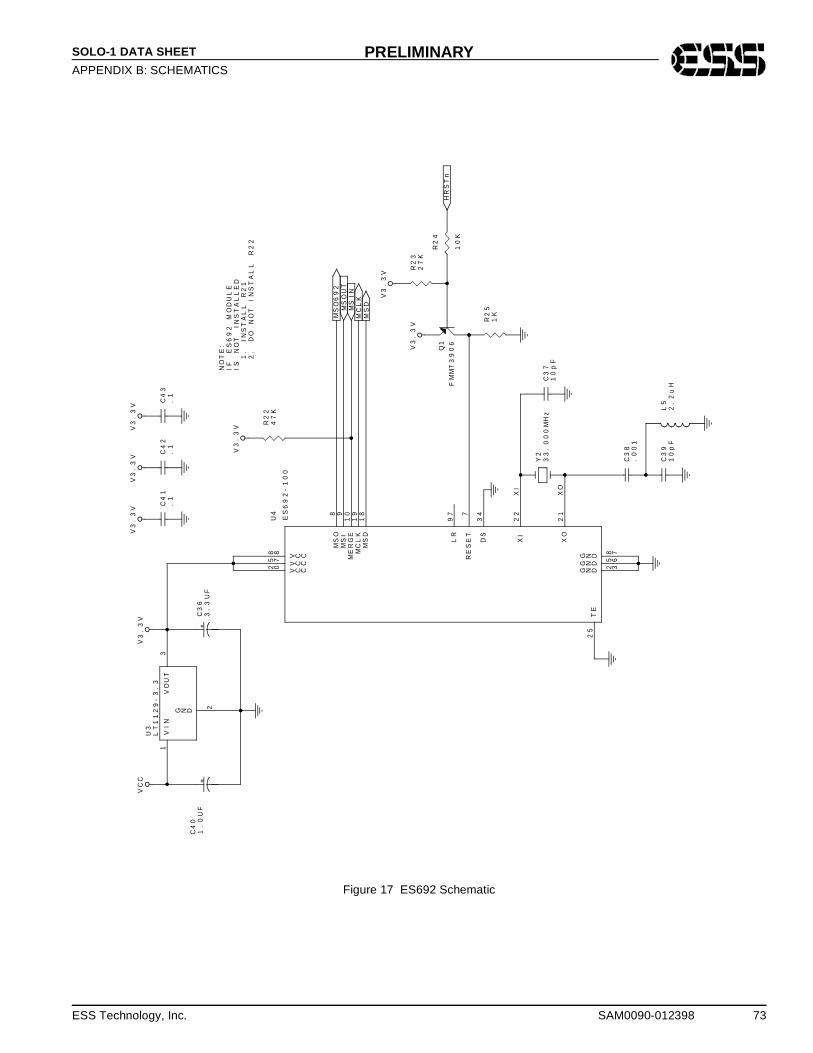
ESS Technology, Inc. SAM0090-012398 73
SOLO-1 DATA SHEET
APPENDIX B: SCHEMATICSPRELIMINARY
Figure 17 ES692 Schematic
V3
.3
VV
3.
3V
V3
.3
V
C4
01
.0
UF
VC
C
VI
N
1
G N D 2
VO
UT
3
U3
LT
11
29
-3
.3
C3
63
.3
UF
C4
1.
1
V3
.3
V
NO
TE
:I
F
ES
69
2
MO
DU
LE
C4
2.
1C
43
.1
IS
N
OT
IN
ST
AL
LE
D
1
.
INS
TA
LL
R
21
2.
D
O
NO
T
IN
ST
AL
L
R2
2
R2
24
7K
V3
.3
V
V C C2 0 V C C5 7 V C C8 8
G N D 5 6G N D 8 7
XO
21
XI
22
TE
2
5
RE
SE
T
7
MS
I
9
MS
D1
8M
CL
K1
9
LR
97
ME
RG
E1
0
MS
O
8
G N D 2 3
DS
34
U4
ES
69
2-
10
0
R2
32
7K
MS
O6
92
MS
INM
SO
UT
MC
LK
MS
D
V3
.3
V
HR
ST
n
R2
4
10
K
R2
51
K
Q1
FM
MT
39
06
V3
.3
V
Y2
33
.0
00
MH
zC
37
10
pF
XO
XI
C3
8.
00
1
C3
91
0p
FL
52
.2
uH

74 SAM0090-012398 ESS Technology, Inc.
SOLO-1 DATA SHEET
APPENDIX B: SCHEMATICSPRELIMINARY
Figure 18 Amplifier
L6 FE
RR
ITE
B
EA
D
R3
4
22
0K
R3
64
70
+1
2V
R2
8
82
0K
C4
41
00
C4
7
.0
1
1
2
3
4
5J
8
3.
5m
m
ST
ER
EO
J
AC
K
SP
EA
KE
RS
L7
FE
RR
ITE
B
EA
D
C5
3
47
0
R2
9
82
0K
1 4
6
8
9
7
13
2
3
1
U5
LM
18
77
C5
1
.1
R3
5
22
0K
C5
2.
01
PC
SP
KO
AO
UT
R
AO
UT
L
C5
5
1.
0u
F
C5
7
1.
0u
F
R3
7
10
0K
R3
8
10
0K
C4
6
.2
2
C5
6
.2
2
R2
6
33
K
R2
7
33
KC
45
47
R3
2
2.
7o
hm
C4
8
.1
R3
3
2.
7o
hm
C4
9
.1
C5
4
47
0
L8
FE
RR
ITE
B
EA
D
R3
0
82
0K
R3
91
0K
R4
01
0K
R3
1
82
0K
C5
0
.0
1
L9
FE
RR
ITE
B
EA
D
1
2
3
4
5J
9
3.
5m
m
ST
ER
EO
J
AC
K
LI
NE
O
UT
L1
0F
ER
RIT
E
BE
AD
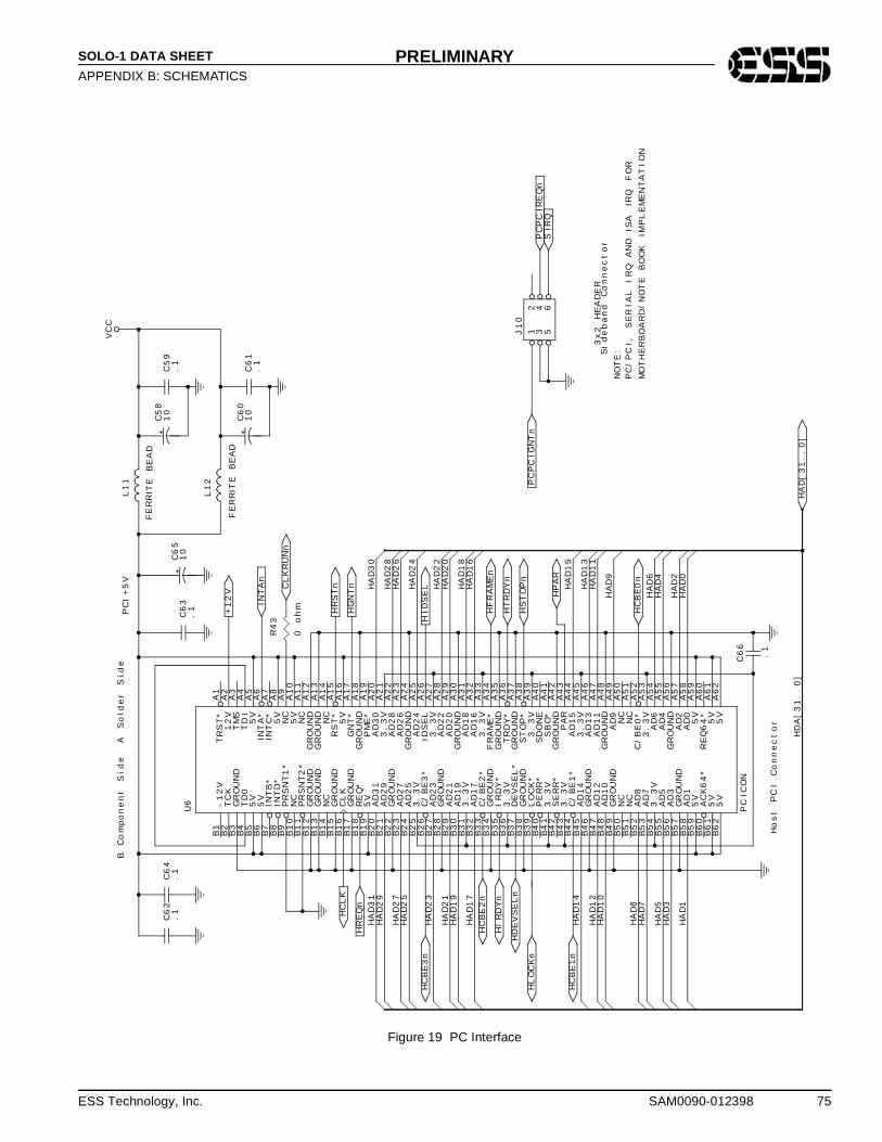
ESS Technology, Inc. SAM0090-012398 75
SOLO-1 DATA SHEET
APPENDIX B: SCHEMATICSPRELIMINARY
Figure 19 PC Interface
VC
C
C5
81
0C
59
.1
L1
1
FE
RR
I TE
B
EA
D
C6
51
0
PC
I+
5V
A
So
lde
r
Sid
eB
C
om
po
ne
nt
S
ide
C6
2.
1C
64
.1
-1
2V
B1
TC
KB
2G
RO
UN
DB
3T
D0
B4
5V
B5
5V
B6
INT
B*
B7
INT
D*
B8
PR
SN
T1
*B
9N
CB
10
PR
SN
T2
*B
11
GR
OU
ND
B1
2G
RO
UN
DB
13
NC
B1
4G
RO
UN
DB
15
CL
KB
16
GR
OU
ND
B1
7R
EQ
*B
18
5V
B1
9A
D3
1B
20
AD
29
B2
1G
RO
UN
DB
22
AD
27
B2
3A
D2
5B
24
3.
3V
B2
5C
/B
E3
*B
26
AD
23
B2
7G
RO
UN
DB
28
AD
21
B2
9A
D1
9B
30
3.
3V
B3
1A
D1
7B
32
C/
BE
2*
B3
3G
RO
UN
DB
34
IR
DY
*B
35
3.
3V
B3
6D
EV
SE
L*
B3
7G
RO
UN
DB
38
LO
CK
*B
39
PE
RR
*B
40
3.
3V
B4
1S
ER
R*
B4
2
TR
ST
*A
11
2V
A2
TM
SA
3T
DI
A4
5V
A5
INT
A*
A6
INT
C*
A7
5V
A8
NC
A9
5V
A1
0N
CA
11
GR
OU
ND
A1
2G
RO
UN
DA
13
NC
A1
4R
ST
*A
15
5V
A1
6G
NT
*A
17
GR
OU
ND
A1
8P
ME
*A
19
AD
30
A2
03
.3
VA
21
AD
28
A2
2A
D2
6A
23
GR
OU
ND
A2
4A
D2
4A
25
IDS
EL
A2
63
.3
VA
27
AD
22
A2
8A
D2
0A
29
GR
OU
ND
A3
0A
D1
8A
31
AD
16
A3
23
.3
VA
33
FR
AM
E*
A3
4G
RO
UN
DA
35
TR
DY
*A
36
GR
OU
ND
A3
7S
TO
P*
A3
83
.3
VA
39
SD
ON
EA
40
SB
O*
A4
1G
RO
UN
DA
42
PA
RA
43
A
D1
5A
44
3.
3V
A4
5A
D1
3A
46
AD
11
A4
7G
RO
UN
DA
48
AD
9A
49
NC
A5
0N
CA
51
C/
BE
0*
A5
23
.3
VA
53
AD
6A
54
AD
4A
55
GR
OU
ND
A5
6A
D2
A5
7A
D0
A5
85
VA
59
RE
Q6
4*
A6
05
VA
61
5V
A6
2
3.
3V
B4
3C
/B
E1
*B
44
AD
14
B4
5G
RO
UN
DB
46
AD
12
B4
7A
D1
0B
48
GR
OU
ND
B4
9N
CB
50
NC
B5
1A
D8
B5
2A
D7
B5
33
.3
VB
54
AD
5B
55
AD
3B
56
GR
OU
ND
B5
7A
D1
B5
85
VB
59
AC
K6
4*
B6
05
VB
61
5V
B6
2
U6
PC
ICO
N
C6
3.
1
INT
An
+1
2V
C6
01
0C
61
.1
L1
2
FE
RR
ITE
B
EA
D
R4
3
0
oh
m HG
NT
n
HR
ST
nCL
KR
UN
n
HC
LK
HR
EQ
n
HC
BE
3n
HA
D3
1H
AD
29
HA
D1
9H
AD
21
HA
D2
5H
AD
27
HA
D2
3H
IDS
ELH
AD
28
HA
D2
2H
AD
20
HA
D2
4
HA
D3
0
HA
D1
8
HA
D2
6
PC
PC
IRE
Qn
SIR
Q
12
34
56
J1
0
3x
2
HE
AD
ER
PC
PC
IGN
Tn
HT
RD
Yn
HS
TO
Pn
HF
RA
ME
n
HP
AR
HA
D1
6H
CB
E2
n
HD
EV
SE
Ln
HI
RD
Yn
HA
D1
7
HL
OC
Kn
HC
BE
1n
HA
D1
0
HA
D7
HA
D8
HA
D1
4
HA
D1
2
HC
BE
0n
HA
D1
1
HA
D1
5
HA
D9
HA
D6
HA
D1
3
Si
de
ba
nd
C
on
ne
ct
or
MO
TH
ER
BO
AR
D/
NO
TE
B
OO
K
IMP
LE
ME
NT
AT
IO
N
PC
/P
CI,
S
ER
I AL
I
RQ
A
ND
IS
A
IRQ
F
OR
NO
TE
:
C6
6
.1
HA
D4
HA
D2
HA
D0
HA
D3
HA
D1
HA
D5
Ho
st
P
CI
Co
nn
ec
to
r
HD
A[
31
..
0]
HA
D[
31
..
0]
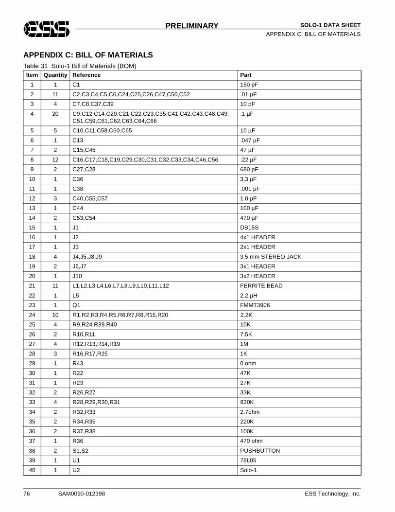
76 SAM0090-012398 ESS Technology, Inc.
SOLO-1 DATA SHEET
APPENDIX C: BILL OF MATERIALSPRELIMINARY
APPENDIX C: BILL OF MATERIALSTable 31 Solo-1 Bill of Materials (BOM) Item Quantity Reference Part
1 1 C1 150 pF
2 11 C2,C3,C4,C5,C6,C24,C25,C26,C47,C50,C52 .01 µF
3 4 C7,C8,C37,C39 10 pF
4 20 C9,C12,C14,C20,C21,C22,C23,C35,C41,C42,C43,C48,C49, C51,C59,C61,C62,C63,C64,C66
.1 µF
5 5 C10,C11,C58,C60,C65 10 µF
6 1 C13 .047 µF
7 2 C15,C45 47 µF
8 12 C16,C17,C18,C19,C29,C30,C31,C32,C33,C34,C46,C56 .22 µF
9 2 C27,C28 680 pF
10 1 C36 3.3 µF
11 1 C38 .001 µF
12 3 C40,C55,C57 1.0 µF
13 1 C44 100 µF
14 2 C53,C54 470 µF
15 1 J1 DB15S
16 1 J2 4x1 HEADER
17 1 J3 2x1 HEADER
18 4 J4,J5,J8,J9 3.5 mm STEREO JACK
19 2 J6,J7 3x1 HEADER
20 1 J10 3x2 HEADER
21 11 L1,L2,L3,L4,L6,L7,L8,L9,L10,L11,L12 FERRITE BEAD
22 1 L5 2.2 µH
23 1 Q1 FMMT3906
24 10 R1,R2,R3,R4,R5,R6,R7,R8,R15,R20 2.2K
25 4 R9,R24,R39,R40 10K
26 2 R10,R11 7.5K
27 4 R12,R13,R14,R19 1M
28 3 R16,R17,R25 1K
29 1 R43 0 ohm
30 1 R22 47K
31 1 R23 27K
32 2 R26,R27 33K
33 4 R28,R29,R30,R31 820K
34 2 R32,R33 2.7ohm
35 2 R34,R35 220K
36 2 R37,R38 100K
37 1 R36 470 ohm
38 2 S1,S2 PUSHBUTTON
39 1 U1 78L05
40 1 U2 Solo-1
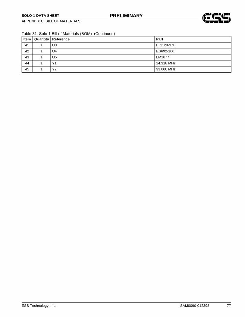
ESS Technology, Inc. SAM0090-012398 77
SOLO-1 DATA SHEET
APPENDIX C: BILL OF MATERIALSPRELIMINARY
41 1 U3 LT1129-3.3
42 1 U4 ES692-100
43 1 U5 LM1877
44 1 Y1 14.318 MHz
45 1 Y2 33.000 MHz
Table 31 Solo-1 Bill of Materials (BOM) (Continued)Item Quantity Reference Part

78 SAM0090-012398 ESS Technology, Inc.
SOLO-1 DATA SHEET
APPENDIX D: LAYOUT GUIDELINESPRELIMINARY
APPENDIX D: LAYOUT GUIDELINES
PCB Layout
Notebook, Motherboard, Pen-based, and PDA portablecomputers have the following similarity in PCB layoutdesign:
1. Multi-layer (usually 4 to 8 layer).
2. Double-sided SMT.
3. CPU, corelogic (chip set), system memory, VGA controller, and video memory reside in the same PCB.
This is a very noisy environment for adding an audiocircuit. The following are the guidelines for PCB layout foran ESS AudioDrive® chip application.
Component PlacementThe audio circuit-related components, including the audioI/O jack and connector, must be grouped in the same area.
There are two possible placements for these audiocomponents:
A grouped on one side of the PCB.
B separated on both sides of the PCB.
In Case B, audio component grouping will take less space.
Analo g Ground PlaneAudio circuits require two layers of analog ground planesfor use as shielding for all analog traces.
In component placement case A (Figure 20), the first layerof analog ground plane is on the analog component side,the second analog ground plane is on the inner layer, andthe analog traces are embedded between these twoplanes.
In component placement case B (Figure 21), the analogground planes are on both sides of the PCB, and theanalog traces are shielded in the middle.
Case A:
Figure 20 Analog Components on One Side of the PCB
Case B:
Figure 21 Analog Components on Both Sides of the PCB
Special NotesThe analog traces should be placed as short as possible.
The MIC-IN circuit is the most sensitive of the audio circuits, and requires proper and complete shielding.
Analog ground plane on analog component side
Inner one or two layer(s) for analog traces
Inner layer analog ground plane
Other layer(s) for digital traces
Components
Analog ground plane on component side
Inner layer(s) for analog traces
Analog ground plane on component sideComponents
Components

ESS Technology, Inc. SAM0090-012398 79
SOLO-1 DATA SHEET
APPENDIX D: LAYOUT GUIDELINESPRELIMINARY
SOLO-1 DATA SHEET
APPENDIX D: LAYOUT GUIDELINESPRELIMINARY
80 © 1998 ESS Technology, Inc. All rights reserved. SAM0090-012398
No part of this publication may be reproduced, stored in aretrieval system, transmitted, or translated in any form orby any means, electronic, mechanical, manual, optical, orotherwise, without the prior written permission of ESSTechnology, Inc.
ESS Technology, Inc. makes no representations orwarranties regarding the content of this document.
All specifications are subject to change without priornotice.
ESS Technology, Inc. assumes no responsibility for anyerrors contained herein.
(P) U.S. Patent 4,214,125 and others, other patentspending.
AudioDrive® and ESPCM® are registered trademarks of ESSTechnology, Inc.
Solo-1TM and ESFMTM are trademarks of ESS Technology,Inc.
All other trademarks are owned by their respectiveholders and are used for identification purposes only.