software modem for a software defined radio system
TRANSCRIPT

Software Modem for a
Software Defined Radio System
Matthys Smuts
Thesis presented in partial fulfilment of the requirements for the degree
Master of Science in Electronic Engineering
at the University of Stellenbosch
Supervisor: Dr G-J van Rooyen
March 2007


Declaration
I, the undersigned, hereby declare that the work contained in this thesis
is my own original work, except where stated otherwise.
Signature Date

Terms of Reference
This thesis was commissioned by Dr. Gert-Jan van Rooyen, lecturer at the University of
Stellenbosch, in 2002. Dr. Gert-Jan van Rooyen’s specific instructions were:
• Explore typical modem architectures used in software defined radios.
• Assume the constraints of the hardware of a desktop computer and seek a suitable
modem standard to implement that could operate on the computer.
• Derive a functional modem based on the above and break it down into smaller
functions or components.
• Investigate the operation of each components in detail and explore an alternative
measure for implementing a generic component.
• Compile a library of these components that is suitable for multiple applications.
• Equip the software framework provided by the existing SDR architecture to comply
to the requirements presented by the modem.
• Demonstrate a working prototype of the modem, with the emphasis on that it will
be for illustrative purposes and not performance enhancement.
i

Abstract
The use of older and slower protocols has become increasingly difficult to justify due to
the rapid pace at which telecommunications are advancing. To keep up to date with the
latest technologies, the communications system must be designed to accommodate the
transparent insertion of new communications standards in all the stages of a system. The
system should, however, also remain compatible with the older standards so as not to
demand an upgrade of the older systems.
The concept of a software defined radio was introduced to overcome these problems. In
a software defined radio system, the functionality of the communications system is defined
in software, which removes the the need for alterations to the hardware during technology
upgrade. To maintain interoperatibilty, the system must be based on a standardised
architecture. This would further allow for enhanced scalability and provide a plug-and-
play feature for the components of the system.
In this thesis, generic signal processing software components are developed to illustrate
the creation of a basic software modem that can be parameterised to comply fully, or
partially, to various standards.
ii

Opsomming
Die gebruik van ouer en stadiger kommunikasie-standaarde word al hoe moeiliker regverdig
as gevolg van die vinnige tred waarteen telekommunikasie vooruitgaan. Om by te hou met
die nuutste tegnologie, moet die kommunikasiestelsel so ontwerp word dat die deursigtige
toevoeging van nuwe kommunikasie-standaarde geakkommodeer kan word in alle fasette
van die stelsel. Die stelsel moet egter ook versoenbaar bly, sodat opgradering van die ouer
sisteme nie benodig word nie.
Om hierdie probleme te oorkom, is die konsep van ’n sagteware-gedefinieerde radio
voorgestel. Die funksionaliteit van die kommunikasiestelsel word in sagteware gedefinieer,
wat beteken dat die hardeware platform nie gewysig hoef te word met die opgradering na
’n nuwe standaard nie. Die stelsel moet op ’n standaard argitektuur gebaseer word sodat
dieselfde koppelvlak tussen die verskillende dele van die stelsel gehandhaaf kan word.
Hierdie sal skalering ook bevoordeel en ’n ”plug-and-play” kenmerk aan die komponente
van die stelsel verskaf.
In hierdie tesis word generiese seinprosesseringskomponente ontwikkel wat gebruik
word om die skepping van ’n basiese sagteware-modem te illustreer, wat ten volle, of
gedeeltelik, aan die spesifikasie van verskeie standaarde voldoen.
iii

Acknowledgements
I would like to thank the following:
• My supervisor, Dr Gert-Jan van Rooyen, for his academic support and guidance
during the course of my studies.
• My friends and colleagues for all their understanding and support, and for realising
the neglect would not continue forever.
• My parents, for their continuous encouragement, support and interest in this en-
deavour. I am forever grateful to you.
• Lastly, I want to thank Charlotte, for all her love, patience and encouragement, and
without whom I would not have managed to reach this goal.
iv

Contents
1 Introduction 1
1.1 Motivation . . . . . . . . . . . . . . . . . . . . . . . . . . . . . . . . . . . . 1
1.2 The Software Defined Radio Architecture of the University of Stellenbosch 2
1.3 Objectives . . . . . . . . . . . . . . . . . . . . . . . . . . . . . . . . . . . . 2
1.4 Thesis layout . . . . . . . . . . . . . . . . . . . . . . . . . . . . . . . . . . 3
2 System level perspective 4
2.1 Software defined radio . . . . . . . . . . . . . . . . . . . . . . . . . . . . . 4
2.1.1 The ideal software radio . . . . . . . . . . . . . . . . . . . . . . . . 4
2.1.2 The practical software radio . . . . . . . . . . . . . . . . . . . . . . 5
2.2 Generic SDR topologies . . . . . . . . . . . . . . . . . . . . . . . . . . . . 6
2.2.1 Digital downconversion . . . . . . . . . . . . . . . . . . . . . . . . . 6
2.2.2 Sample rate conversion . . . . . . . . . . . . . . . . . . . . . . . . . 7
2.2.3 Channelisation . . . . . . . . . . . . . . . . . . . . . . . . . . . . . 7
2.2.4 Baseband processing . . . . . . . . . . . . . . . . . . . . . . . . . . 8
2.3 Conceptual design of the softmodem . . . . . . . . . . . . . . . . . . . . . 9
2.3.1 Defining draft specifications . . . . . . . . . . . . . . . . . . . . . . 9
2.3.2 Modem standards for the telephone channel . . . . . . . . . . . . . 9
2.3.3 Softmodem projects . . . . . . . . . . . . . . . . . . . . . . . . . . . 12
2.3.4 Finalising the specifications . . . . . . . . . . . . . . . . . . . . . . 13
2.4 Block diagram design . . . . . . . . . . . . . . . . . . . . . . . . . . . . . . 13
2.4.1 Design considerations . . . . . . . . . . . . . . . . . . . . . . . . . . 13
2.4.2 Transmitter design . . . . . . . . . . . . . . . . . . . . . . . . . . . 14
2.4.3 Receiver design . . . . . . . . . . . . . . . . . . . . . . . . . . . . . 15
2.5 Conclusion . . . . . . . . . . . . . . . . . . . . . . . . . . . . . . . . . . . . 16
3 Transmitter of the softmodem 18
3.1 Scrambler . . . . . . . . . . . . . . . . . . . . . . . . . . . . . . . . . . . . 18
3.2 Bit-to-integer converter . . . . . . . . . . . . . . . . . . . . . . . . . . . . . 19
3.3 Differential encoding . . . . . . . . . . . . . . . . . . . . . . . . . . . . . . 21
3.4 Trellis coded modulation . . . . . . . . . . . . . . . . . . . . . . . . . . . . 21
v

CONTENTS vi
3.4.1 Convolutional codes for TCM . . . . . . . . . . . . . . . . . . . . . 23
3.4.2 Implementation of the convolutional encoder . . . . . . . . . . . . 24
3.4.3 Standalone binary convolutional encoder . . . . . . . . . . . . . . . 26
3.4.4 Set partitioning . . . . . . . . . . . . . . . . . . . . . . . . . . . . . 27
3.4.5 Implementation of the lookup table component . . . . . . . . . . . 28
3.5 Pulse shape filtering . . . . . . . . . . . . . . . . . . . . . . . . . . . . . . 28
3.5.1 Raised cosine filter . . . . . . . . . . . . . . . . . . . . . . . . . . . 29
3.5.2 Implementation of the interpolator . . . . . . . . . . . . . . . . . . 31
3.6 Quadrature modulator . . . . . . . . . . . . . . . . . . . . . . . . . . . . . 34
3.7 Conclusion . . . . . . . . . . . . . . . . . . . . . . . . . . . . . . . . . . . . 35
4 Receiver of the softmodem 37
4.1 Automatic gain control . . . . . . . . . . . . . . . . . . . . . . . . . . . . . 37
4.1.1 Gain error detector . . . . . . . . . . . . . . . . . . . . . . . . . . . 38
4.1.2 Mode selection . . . . . . . . . . . . . . . . . . . . . . . . . . . . . 38
4.1.3 Signal presence detection . . . . . . . . . . . . . . . . . . . . . . . . 40
4.1.4 Evaluation of the AGC . . . . . . . . . . . . . . . . . . . . . . . . . 40
4.2 Quadrature demodulator . . . . . . . . . . . . . . . . . . . . . . . . . . . . 42
4.2.1 Implementation of the demodulator . . . . . . . . . . . . . . . . . . 43
4.3 Symbol timing recovery . . . . . . . . . . . . . . . . . . . . . . . . . . . . . 44
4.3.1 Polynomial-based interpolation filter . . . . . . . . . . . . . . . . . 45
4.3.2 Timing error detector . . . . . . . . . . . . . . . . . . . . . . . . . . 48
4.3.3 Loop filter . . . . . . . . . . . . . . . . . . . . . . . . . . . . . . . . 49
4.3.4 Evaluation of the symbol synchroniser . . . . . . . . . . . . . . . . 51
4.4 Carrier synchronisation . . . . . . . . . . . . . . . . . . . . . . . . . . . . . 53
4.4.1 Phase rotator . . . . . . . . . . . . . . . . . . . . . . . . . . . . . . 54
4.4.2 Phase error detector . . . . . . . . . . . . . . . . . . . . . . . . . . 55
4.4.3 Loop filter . . . . . . . . . . . . . . . . . . . . . . . . . . . . . . . . 56
4.4.4 Evaluation of the carrier synchroniser . . . . . . . . . . . . . . . . 57
4.5 Adaptive equalisation . . . . . . . . . . . . . . . . . . . . . . . . . . . . . . 58
4.5.1 Least mean-square equaliser . . . . . . . . . . . . . . . . . . . . . . 59
4.5.2 Step-size parameter . . . . . . . . . . . . . . . . . . . . . . . . . . . 59
4.5.3 Evaluation of the LMS equaliser . . . . . . . . . . . . . . . . . . . . 60
4.6 Viterbi decoding . . . . . . . . . . . . . . . . . . . . . . . . . . . . . . . . 60
4.6.1 Initialisation . . . . . . . . . . . . . . . . . . . . . . . . . . . . . . . 61
4.6.2 Minimum distance calculation . . . . . . . . . . . . . . . . . . . . . 63
4.6.3 Accumulated distance to each state . . . . . . . . . . . . . . . . . . 63
4.6.4 Trace back and output . . . . . . . . . . . . . . . . . . . . . . . . . 65
4.6.5 Decision device . . . . . . . . . . . . . . . . . . . . . . . . . . . . . 65

CONTENTS vii
4.6.6 Evaluation of the Viterbi decoder . . . . . . . . . . . . . . . . . . . 66
4.7 Differential decoding . . . . . . . . . . . . . . . . . . . . . . . . . . . . . . 67
4.8 Integer-to-bit conversion . . . . . . . . . . . . . . . . . . . . . . . . . . . . 67
4.9 Data descrambling . . . . . . . . . . . . . . . . . . . . . . . . . . . . . . . 68
4.10 Conclusion . . . . . . . . . . . . . . . . . . . . . . . . . . . . . . . . . . . . 68
5 Implementation in the SDR Architecture 70
5.1 Overview of SDR architecture . . . . . . . . . . . . . . . . . . . . . . . . . 70
5.1.1 The converter layer . . . . . . . . . . . . . . . . . . . . . . . . . . . 71
5.1.2 The subcontroller . . . . . . . . . . . . . . . . . . . . . . . . . . . . 72
5.1.3 The main application . . . . . . . . . . . . . . . . . . . . . . . . . . 72
5.2 Modem implementation . . . . . . . . . . . . . . . . . . . . . . . . . . . . 73
5.2.1 Overview of software components . . . . . . . . . . . . . . . . . . . 73
5.2.2 Modem Controller . . . . . . . . . . . . . . . . . . . . . . . . . . . 73
5.2.3 Modem controller at transfer initiation . . . . . . . . . . . . . . . . 74
5.2.4 The modem in the SDR architecture . . . . . . . . . . . . . . . . . 76
5.3 Concepts implemented for improved robustness and functionality . . . . . . 76
5.3.1 Modifications to the architecture . . . . . . . . . . . . . . . . . . . 76
6 Measurements and results 80
6.1 Evaluation setup overview . . . . . . . . . . . . . . . . . . . . . . . . . . . 80
6.2 Evaluation on component level . . . . . . . . . . . . . . . . . . . . . . . . . 81
6.2.1 Purpose of the experiment . . . . . . . . . . . . . . . . . . . . . . . 81
6.2.2 Experimental setup . . . . . . . . . . . . . . . . . . . . . . . . . . . 82
6.2.3 Results . . . . . . . . . . . . . . . . . . . . . . . . . . . . . . . . . . 82
6.3 Overall performance of the softmodem . . . . . . . . . . . . . . . . . . . . 88
6.3.1 Purpose of the experiment . . . . . . . . . . . . . . . . . . . . . . . 88
6.3.2 Experimental setup . . . . . . . . . . . . . . . . . . . . . . . . . . . 88
6.3.3 Results . . . . . . . . . . . . . . . . . . . . . . . . . . . . . . . . . . 88
6.4 Conclusion . . . . . . . . . . . . . . . . . . . . . . . . . . . . . . . . . . . . 91
7 Conclusion 93
7.1 Overview of the work . . . . . . . . . . . . . . . . . . . . . . . . . . . . . . 93
7.2 Future work . . . . . . . . . . . . . . . . . . . . . . . . . . . . . . . . . . . 96

List of Figures
2.1 The ideal software radio . . . . . . . . . . . . . . . . . . . . . . . . . . . . 4
2.2 Generic but feasible software defined radio . . . . . . . . . . . . . . . . . . 5
2.3 The generic receiver in detail . . . . . . . . . . . . . . . . . . . . . . . . . . 6
2.4 A simple representation of the sample rate converter . . . . . . . . . . . . 7
2.5 V.34 vs V.90: methods of connection . . . . . . . . . . . . . . . . . . . . . 11
2.6 Block diagram of the V.32 bis transmitter . . . . . . . . . . . . . . . . . . 15
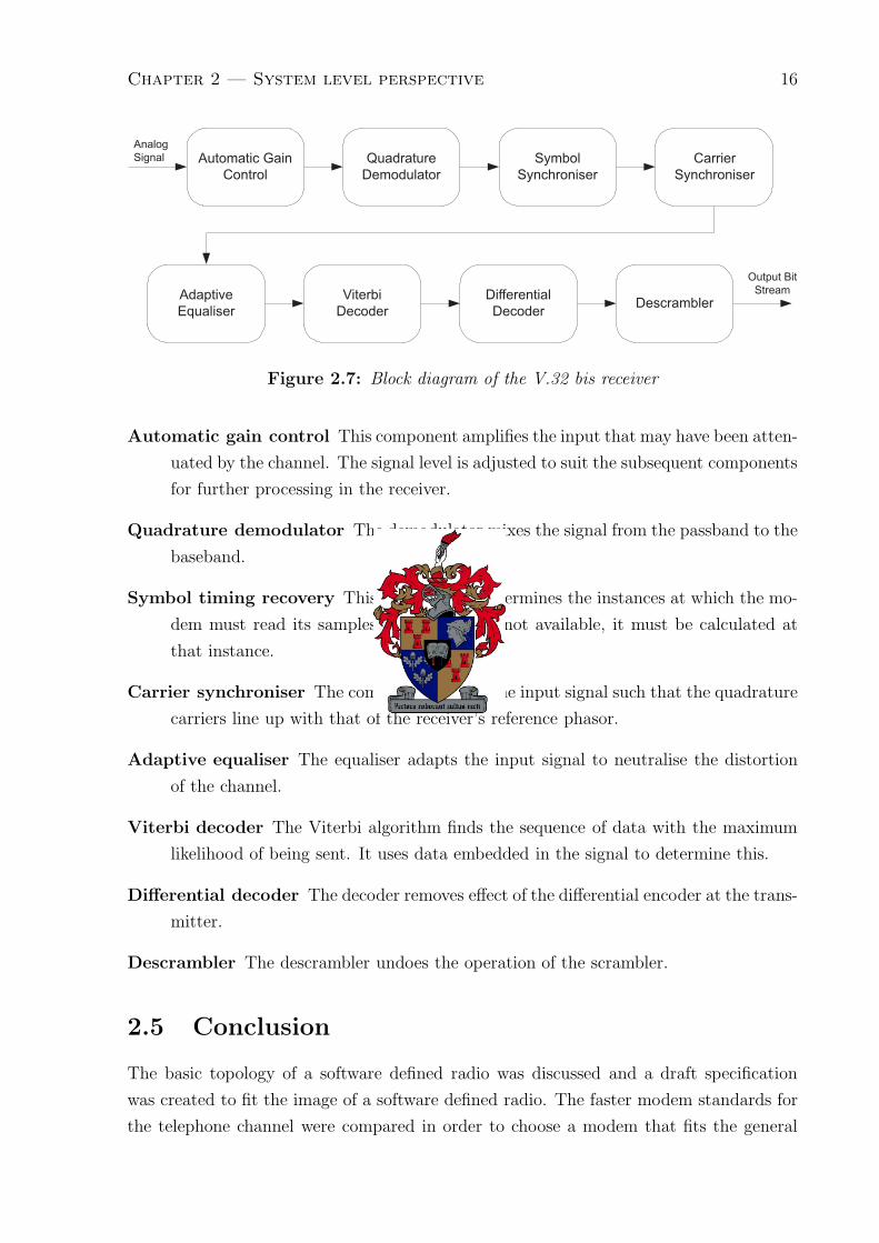
2.7 Block diagram of the V.32 bis receiver . . . . . . . . . . . . . . . . . . . . 16
3.1 The scrambler used in the V.32 bis standard . . . . . . . . . . . . . . . . . 19
3.2 Bit-to-integer converter . . . . . . . . . . . . . . . . . . . . . . . . . . . . . 20
3.3 Lookup tables for the coded (left) and uncoded (right) differential encoders
of V.32 bis standard. y(n−1) is the previous output and x(n) is the current
input. . . . . . . . . . . . . . . . . . . . . . . . . . . . . . . . . . . . . . . 22
3.4 General structure of the encoder and modulator for a trellis coded modulator 23
3.5 The feedback convolutional encoder defined in V.32 bis . . . . . . . . . . . 23
3.6 Trellis diagram for the convolutional encoder of Figure 3.5 . . . . . . . . . 24
3.7 The state transition lookup table for the convolutional encoder in Fig-
ure 3.5. z(n) is the current state and x(n) is the input. . . . . . . . . . . . 25
3.8 The output lookup table for the convolutional encoder in Figure 3.5. z(n)
is the current state and x(n) is the input. . . . . . . . . . . . . . . . . . . . 26
3.9 Set partitioning of the 16-QAM signal as defined in V.32 bis . . . . . . . . 27
3.10 Lookup table implementation for a two dimensional table . . . . . . . . . . 28
3.11 Frequency response of the raised cosine filter for α = 0, 0.25 and 0.5 . . . . 30
3.12 Rate conversion with a time-continuous filter . . . . . . . . . . . . . . . . . 31
3.13 Sample time relation . . . . . . . . . . . . . . . . . . . . . . . . . . . . . . 32
3.14 Realisation of the sampling rate conversion by a rational factor I/D [33] . 33
3.15 The quadrature modulator of the modem . . . . . . . . . . . . . . . . . . . 34
3.16 The transmitter as defined by V.32 bis . . . . . . . . . . . . . . . . . . . . 36
4.1 Block diagram of the AGC . . . . . . . . . . . . . . . . . . . . . . . . . . . 38
4.2 The gain error detector curve for energy levels ranging from 0.001 to 10 . . 39
viii

LIST OF FIGURES ix
4.3 AGC operating modes . . . . . . . . . . . . . . . . . . . . . . . . . . . . . 40
4.4 Response of the AGC to a low energy signal . . . . . . . . . . . . . . . . . 41
4.5 Quadrature demodulator and the image rejection filter . . . . . . . . . . . 43
4.6 Block diagram of the symbol synchroniser . . . . . . . . . . . . . . . . . . 45
4.7 Impulse response of the linear and cubic interpolating polynomial . . . . . 46
4.8 Farrow structure for a cubic interpolator . . . . . . . . . . . . . . . . . . . 48
4.9 The S-curve for various values of the roll off factor . . . . . . . . . . . . . . 50
4.10 Typical response of the symbol synchroniser . . . . . . . . . . . . . . . . . 52
4.11 Rotated 16-QAM constellation due to unknown initial phase and frequency
offset . . . . . . . . . . . . . . . . . . . . . . . . . . . . . . . . . . . . . . . 53
4.12 Block diagram of the carrier synchroniser . . . . . . . . . . . . . . . . . . . 55
4.13 Phase error detector curve . . . . . . . . . . . . . . . . . . . . . . . . . . . 56
4.14 Phase error signal achieving lock . . . . . . . . . . . . . . . . . . . . . . . . 57
4.15 Adaptive equaliser . . . . . . . . . . . . . . . . . . . . . . . . . . . . . . . 58
4.16 Flow diagram for the Viterbi decoder . . . . . . . . . . . . . . . . . . . . . 62
4.17 The state transition lookup table for the Viterbi decoder. z(n) and z(n-1)
are the current and previous state. . . . . . . . . . . . . . . . . . . . . . . 64
4.18 The output lookup table for the Viterbi decoder. z(n) and z(n-1) are the
current and previous state. . . . . . . . . . . . . . . . . . . . . . . . . . . . 64
4.19 The inverse tables of the differential encoder as calculated by the decoder.
x(n) and x(n-1) are the current and previous input. . . . . . . . . . . . . . 67
4.20 The integer-to-bit converter . . . . . . . . . . . . . . . . . . . . . . . . . . 68
4.21 A descrambler for the V.32 bis standard . . . . . . . . . . . . . . . . . . . 68
4.22 The complete receiver of the V.32 bis modem . . . . . . . . . . . . . . . . 69
5.1 The architecture of the software defined radio system . . . . . . . . . . . . 71
5.2 The SDR converter . . . . . . . . . . . . . . . . . . . . . . . . . . . . . . . 72
5.3 Initialisation and training sequences defined in V.32 bis . . . . . . . . . . . 74
5.4 The modem as implemented in the SDR architecture. . . . . . . . . . . . . 77
5.5 Signal flow of the modified subcontroller . . . . . . . . . . . . . . . . . . . 78
6.1 The setup with which the modem was evaluated . . . . . . . . . . . . . . . 80
6.2 The frequency response of the channel used in the simulation. The sampling
rate is 8000Hz . . . . . . . . . . . . . . . . . . . . . . . . . . . . . . . . . . 81
6.3 The gain of the AGC component during initialisation and data transfer . . 83
6.4 The error signal of the timing error detector . . . . . . . . . . . . . . . . . 84
6.5 The phase error of the carrier synchroniser . . . . . . . . . . . . . . . . . . 85
6.6 The LMS error signal of the adaptive equaliser . . . . . . . . . . . . . . . . 86
6.7 The real part of the constellation at the output of the adaptive equaliser . 87

LIST OF FIGURES x
6.8 Symbol error rate for the 16-QAM modem . . . . . . . . . . . . . . . . . . 89
6.9 Measured SNR vs input SNR . . . . . . . . . . . . . . . . . . . . . . . . . 90
6.10 Deduced symbol error rate for the 16-QAM modem . . . . . . . . . . . . . 92

List of Tables
3.1 Scrambler attributes . . . . . . . . . . . . . . . . . . . . . . . . . . . . . . 19
3.2 Bit-to-integer converter attribute . . . . . . . . . . . . . . . . . . . . . . . 20
3.3 Differential encoder attributes . . . . . . . . . . . . . . . . . . . . . . . . . 22
3.4 Convolutional encoder attributes . . . . . . . . . . . . . . . . . . . . . . . 26
3.5 The lookup table attribute . . . . . . . . . . . . . . . . . . . . . . . . . . . 28
3.6 Interpolator attributes . . . . . . . . . . . . . . . . . . . . . . . . . . . . . 34
3.7 Quadrature modulator attribute . . . . . . . . . . . . . . . . . . . . . . . . 35
4.1 Automatic gain control attributes . . . . . . . . . . . . . . . . . . . . . . . 42
4.2 Quadrature demodulator attribute . . . . . . . . . . . . . . . . . . . . . . 43
4.3 Filter attributes . . . . . . . . . . . . . . . . . . . . . . . . . . . . . . . . . 44
4.4 Farrow coefficients for a cubic interpolator . . . . . . . . . . . . . . . . . . 48
4.5 Symbol synchroniser . . . . . . . . . . . . . . . . . . . . . . . . . . . . . . 53
4.6 Carrier synchroniser attributes . . . . . . . . . . . . . . . . . . . . . . . . . 58
4.7 LMS attributes . . . . . . . . . . . . . . . . . . . . . . . . . . . . . . . . . 60
4.8 Viterbi decoder attributes . . . . . . . . . . . . . . . . . . . . . . . . . . . 66
4.9 Differential decoder attribute . . . . . . . . . . . . . . . . . . . . . . . . . 67
4.10 Integer-to-bit converter attribute . . . . . . . . . . . . . . . . . . . . . . . 67
4.11 Descrambler attribute . . . . . . . . . . . . . . . . . . . . . . . . . . . . . 69
5.1 Attributes changed by modem controller for stage 3 . . . . . . . . . . . . . 75
6.1 Expected packet loss rates for various SNR . . . . . . . . . . . . . . . . . . 91
6.2 Number of packets lost for various SNR . . . . . . . . . . . . . . . . . . . . 91
xi

Nomenclature
Acronyms
ADC Analog to Digital Converter
AGC Automatic Gain Control
BPSK Binary Phase Shift Keying
DAC Digital to Analog Converter
DFPLL Decision Feedback Phase Lock Loop
GP Generating Polynomial
IF Intermediate Frequency
ISI Intersymbol Interference
ITU International Telecommunications Union
LMS Least Mean Square
LPF Low Pass Filter
M-PSK M-ary Phase Shift Keying
M-QAM M-ary Quadrature Amplitude Modulation
MSE Mean Square Equiliser
NCO Numerical Controlled Oscillator
PCM Pulse Coded Modulation
PI Plus Integral
PLL Phase Lock Loop
PSK Phase Shift Key
PSTN Public Switched Telephone Network
QAM Quadrature Amplitude Modulation
QPSK Quadrature Phase Shift Key
RF Radio Frequency
SNR Signal to Noise Ratio
TCM Trellis Coded Modulation
xii

LIST OF TABLES xiii
Symbols
x(∗) General input
y(∗) General output
bps Bits per second
sps Symbols per second
C Channel capacity
W Signal bandwidth
fc Cutoff or Carrier frequency
fs Sampling rate
fd Data or Symbol rate
m TCM input bit number
m Convolutional input bit number
P (f) Frequency response
α Rolloff factor of Raised Cosine Filter
μk Fractional interval
D Decimation factor
I Interpolation factor
Eref Reference energy level
G,g Gain
N Degree of polynomial-based filter

Chapter 1
Introduction
1.1 Motivation
With the ever increasing demand for bandwidth as well as mobility, the search for a faster
yet economically viable communications platforms will never subside. This market driven
force is exploited by many service providers to increase profits, yet the goal to unify all
communications always seems to come second. However, in the future only a few users
will agree to purchasing dedicated terminals for different services in different networks.
Furthermore, equipment manufacturers will also be able to reduce costs of their products
by unifying the hardware platform.
By looking at current and emerging standards in the mobile telecommunications mar-
ket, it is clear that the different technologies used to transfer information via radio by the
various standards, are limited. The three basic methods of channel accessing are TDMA,
FDMA and CDMA and can even be further subdivided and differentiated because other
characteristics such as modulation scheme, antenna beamforming and error correction are
also employed. To combine this diversity in different schemes into one common terminal
platform, the need arises for software parameterisable and programmable terminals.
These are the main drives behind the software defined radio concept and equipment
manufactures are all pursuing this course with their products. The goal of producing the
ideal software terminal that supports all standards are, however, still a long way off. Due
to the limitation of processing power, for example, it is not yet possible for a hardware
platform to address a variety of specific channel access schemes or standards. Research to
improve the common hardware terminal and especially in unifying the different accessing
schemes into one all-embracing algorithm, will always be needed to feed the great demand
for global access to information.
1

Chapter 1 — Introduction 2
1.2 The Software Defined Radio Architecture of the
University of Stellenbosch
The Telecoms group at the University of Stellenbosch’s started a software defined radio
study group to pursue and explore the field of software radios. A software architecture or
framework was developed to enable rapid development of new software radio components
and applications. The main requirements for the architecture was that it should be
efficient for signal processing and it should be portable across various hardware platforms
with as few implementation issues as possible. This architecture will form the basis for
this project.
1.3 Objectives
The main objective of this thesis is to implement a generic software modem in the software
defined radio architecture of the University of Stellenbosch. The modem must receive data
in binary format, modulate it for transmission over a channel and at the receiver side,
successfully convert the signal back into the original data. The process of achieving this
goal is summed up by the following objectives:
• Study the typical topologies of software defined radio systems and study these sys-
tems’ relation to conventional modem implementations.
• Assume the constraints provided by a typical desktop computer and seek a suitable
modem standard to implement that could operate on the computer.
• Derive a functional modem based on the modem standard mentioned above and
break it down into smaller functions or components.
• Carry out research into the operation of each component of the modem in order to
create a generic component suitable for various applications.
• Compile a library of these components that is suitable for multiple applications.
• Equip the software framework provided by the existing SDR architecture to comply
to the requirements presented by the modem.
• Provide a working prototype of the modem with the emphasis on that it will be
for illustrative purposes and not to enhance the performance of the implemented
standard.

Chapter 1 — Introduction 3
1.4 Thesis layout
The first few objectives presented in the previous section, are studied in Chapter 2 and
provides the background required to establish a design for the software modem. The
typical functional components found in software defined radio are presented followed by
a draft design of the modem that fits into this model. The chapter concludes with a
functional design of the transmitter and the receiver of the software modem.
Chapter 3 presents the design of the transmitter. Each of the functional components
are discussed in detail and their working confirmed after implementation.
The receiver of the modem is given in Chapter 4. Here the detailed study of each
component is continued as well as an evaluation of the components. Both this chapter
and the previous one ends with a diagram that embodies all the components into the
transmitter or receiver.
The subject of Chapter 5 involves the implementation of the modem into the software
defined radio architecture of the University of Stellenbosch. A map of the modem, showing
all the routes between the different components, is shown and the implementation of the
modem controller is discussed. The chapter ends with a summary of the alterations to
the architecture that was required for the modem to work.
Chapter 6 presents the measurements and results of the evaluation process of the mo-
dem. The evaluation of the components is performed followed by the overall performance
evaluation of the software modem.

Chapter 2
System level perspective
A good definition of a software radio is a radio that is substantially defined in software
and of which the physical layer behaviour can be significantly altered through changes to
its software [35]. This idea underlies this project, but first some introductory information
is needed. This chapter provides an overview of software defined radio concepts in general,
from which the draft specification is deduced. This is followed by a further investigation
into applicable standards, which are used as basis for a final description of the software
modem and its components.
2.1 Software defined radio
2.1.1 The ideal software radio
The ideal software radio is a system that uses minimal analog components. The software
radio converts the RF signal from an analog signal to a digital signal directly at the
antenna. The minimum number of analog components are used in the RF portion only
and all subsequent processing is done in the digital domain. Such a radio is depicted in
Figure 2.1.
The ability of the radio to achieve this is mostly determine by the specifications of
the conversion and processing operations. Firstly, the analog to digital converter must
ADC
Software
Processing
Engine
User/
Application
Interaction
Antenna
Figure 2.1: The ideal software radio
4
Chapter 2 — System level perspective 5
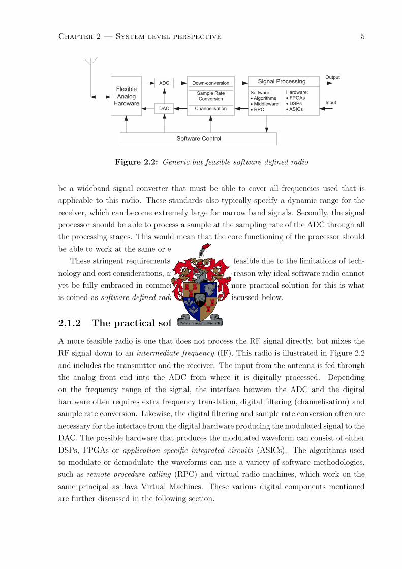
ADC
Flexible
Analog
Hardware
Software Control
ChannelisationDAC
Signal ProcessingOutput
Input
Hardware:
� FPGAs
� DSPs
� ASICs
Software:
� Algorithms
� Middleware
� RPC
Down-conversion
Sample Rate
Conversion
Figure 2.2: Generic but feasible software defined radio
be a wideband signal converter that must be able to cover all frequencies used that is
applicable to this radio. These standards also typically specify a dynamic range for the
receiver, which can become extremely large for narrow band signals. Secondly, the signal
processor should be able to process a sample at the sampling rate of the ADC through all
the processing stages. This would mean that the core functioning of the processor should
be able to work at the same or even higher rate.
These stringent requirements are generally not feasible due to the limitations of tech-
nology and cost considerations, and is therefore the reason why ideal software radio cannot
yet be fully embraced in commercial systems. A more practical solution for this is what
is coined as software defined radio (SDR) and is discussed below.
2.1.2 The practical software radio
A more feasible radio is one that does not process the RF signal directly, but mixes the
RF signal down to an intermediate frequency (IF). This radio is illustrated in Figure 2.2
and includes the transmitter and the receiver. The input from the antenna is fed through
the analog front end into the ADC from where it is digitally processed. Depending
on the frequency range of the signal, the interface between the ADC and the digital
hardware often requires extra frequency translation, digital filtering (channelisation) and
sample rate conversion. Likewise, the digital filtering and sample rate conversion often are
necessary for the interface from the digital hardware producing the modulated signal to the
DAC. The possible hardware that produces the modulated waveform can consist of either
DSPs, FPGAs or application specific integrated circuits (ASICs). The algorithms used
to modulate or demodulate the waveforms can use a variety of software methodologies,
such as remote procedure calling (RPC) and virtual radio machines, which work on the
same principal as Java Virtual Machines. These various digital components mentioned
are further discussed in the following section.
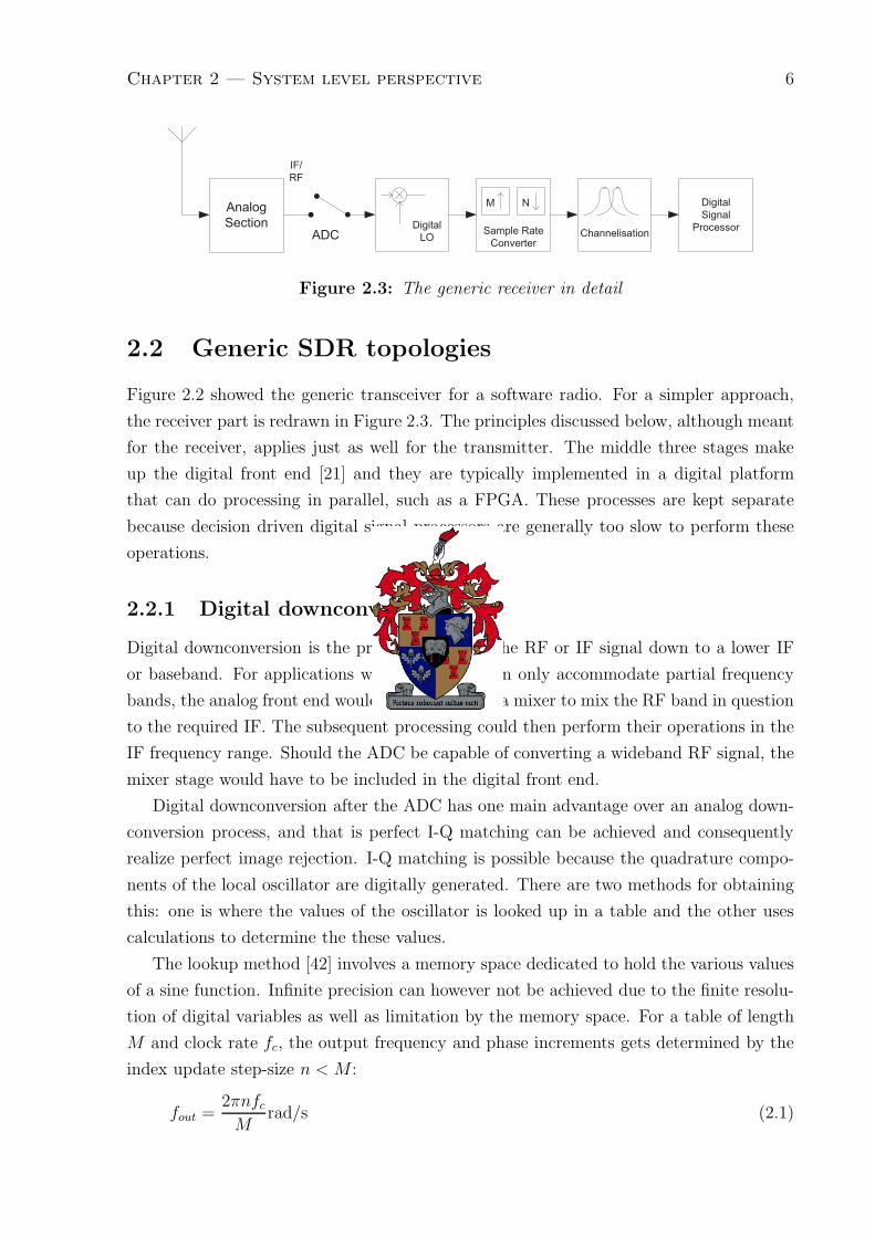
Chapter 2 — System level perspective 6
Analog
SectionSample Rate
Converter
IF/
RF
ADC Channelisation
Digital
Signal
ProcessorDigital
LO
M N
Figure 2.3: The generic receiver in detail
2.2 Generic SDR topologies
Figure 2.2 showed the generic transceiver for a software radio. For a simpler approach,
the receiver part is redrawn in Figure 2.3. The principles discussed below, although meant
for the receiver, applies just as well for the transmitter. The middle three stages make
up the digital front end [21] and they are typically implemented in a digital platform
that can do processing in parallel, such as a FPGA. These processes are kept separate
because decision driven digital signal processors are generally too slow to perform these
operations.
2.2.1 Digital downconversion
Digital downconversion is the process of mixing the RF or IF signal down to a lower IF
or baseband. For applications where the ADC can only accommodate partial frequency
bands, the analog front end would have to include a mixer to mix the RF band in question
to the required IF. The subsequent processing could then perform their operations in the
IF frequency range. Should the ADC be capable of converting a wideband RF signal, the
mixer stage would have to be included in the digital front end.
Digital downconversion after the ADC has one main advantage over an analog down-
conversion process, and that is perfect I-Q matching can be achieved and consequently
realize perfect image rejection. I-Q matching is possible because the quadrature compo-
nents of the local oscillator are digitally generated. There are two methods for obtaining
this: one is where the values of the oscillator is looked up in a table and the other uses
calculations to determine the these values.
The lookup method [42] involves a memory space dedicated to hold the various values
of a sine function. Infinite precision can however not be achieved due to the finite resolu-
tion of digital variables as well as limitation by the memory space. For a table of length
M and clock rate fc, the output frequency and phase increments gets determined by the
index update step-size n < M :
fout =2πnfc
Mrad/s (2.1)
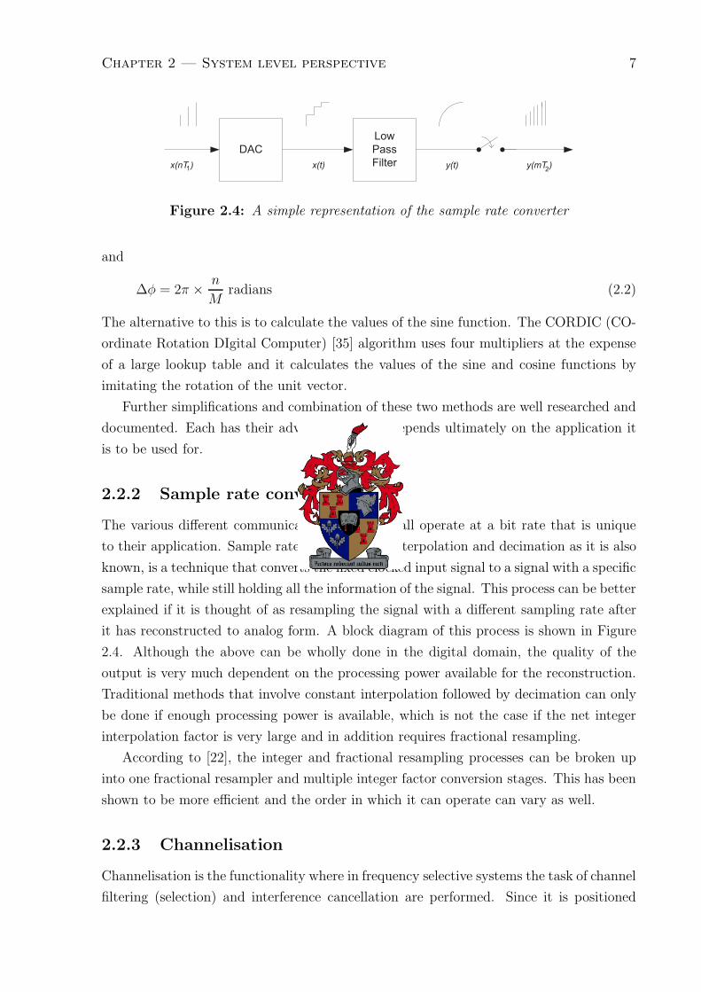
Chapter 2 — System level perspective 7
DAC
x(nT )
Low
Pass
Filter1 2
x(t) y(t) y(mT )
Figure 2.4: A simple representation of the sample rate converter
and
Δφ = 2π × n
Mradians (2.2)
The alternative to this is to calculate the values of the sine function. The CORDIC (CO-
ordinate Rotation DIgital Computer) [35] algorithm uses four multipliers at the expense
of a large lookup table and it calculates the values of the sine and cosine functions by
imitating the rotation of the unit vector.
Further simplifications and combination of these two methods are well researched and
documented. Each has their advantages and it depends ultimately on the application it
is to be used for.
2.2.2 Sample rate conversion
The various different communications standards all operate at a bit rate that is unique
to their application. Sample rate conversion, or interpolation and decimation as it is also
known, is a technique that converts the fixed clocked input signal to a signal with a specific
sample rate, while still holding all the information of the signal. This process can be better
explained if it is thought of as resampling the signal with a different sampling rate after
it has reconstructed to analog form. A block diagram of this process is shown in Figure
2.4. Although the above can be wholly done in the digital domain, the quality of the
output is very much dependent on the processing power available for the reconstruction.
Traditional methods that involve constant interpolation followed by decimation can only
be done if enough processing power is available, which is not the case if the net integer
interpolation factor is very large and in addition requires fractional resampling.
According to [22], the integer and fractional resampling processes can be broken up
into one fractional resampler and multiple integer factor conversion stages. This has been
shown to be more efficient and the order in which it can operate can vary as well.
2.2.3 Channelisation
Channelisation is the functionality where in frequency selective systems the task of channel
filtering (selection) and interference cancellation are performed. Since it is positioned
Chapter 2 — System level perspective 8
after the sample rate converter, the received signal has already undergone coarse channel
selection and interference cancellation due to the low pass filters in the decimation filter.
Thus the channelisation only has to perform the fine, sharp cutoff filtering.
Channelisation further often shares this part of the digital front end with a de-
spreading component. De-spreading is the functionality where in spread spectrum systems
the task of decorrellation and sample rate decimation to symbol rate is realized. It can
also be viewed as a type of matched filtering at symbol level. It is suggested that both
can be implemented within the same algorithm since they share the same mathematical
operations, but the execution speed of the digital platform needs to be very high to be
effective.
The output of the channelisation process is also the output of the front end and it is
characterised by having a sample rate determined by the current protocol interface. This
digital signal represents the channel of interest, which could but not necessarily be at
baseband. Thus the front end of a digital receiver must provide a digital signal
1. of a certain bandwidth,
2. at a certain centre frequency, and
3. with a certain sample rate.
The signal is now exported to the digital signal processor for further decoding and de-
modulation.
2.2.4 Baseband processing
The baseband processing engine of a radio system is used to digitally transform the raw
data stream for transmission over a channel. The transmitter formats the data into a more
usable form and introduces redundancy should it be required by the specific standard.
The receiver’s operations are, however, more intensive as the signal received from the
radio front end has to be scrutinised in order for it to extract the correct data from it as
intended.
The operations performed in the digital signal processor include synchronisation, de-
modulation, channel equalisation, channel (de)coding, and multiple access channel extrac-
tion. All of these components are linked together to form a chain of a signal processors,
providing a pathway for the data to pass through.
The type of hardware used is mostly determined by the channel of interest as well
as the other functions the hardware must perform. The quality of reception is greatly
determined by the complexity of the algorithms used and thus the better the processor,
the better the reception. The processor requirement can also vary per application, thus
it should cater for all these possibilities.

Chapter 2 — System level perspective 9
The various hardware platforms available are compared in [9], with the advantages
and disadvantages discussed for each. A more detailed look into baseband processing can
be found in [39].
2.3 Conceptual design of the softmodem
The concepts discussed up to this point were to illustrate the basic structure of a typical
software defined radio. These concepts are now taken further by using them as a template
to draw up preliminary specifications for a softmodem. A further in-depth study of
standards is concluded with the finalisation of the softmodem specifications.
2.3.1 Defining draft specifications
The topics that were covered thus far only revolved around radio frequency terminals.
Radio has become the dominant means of communication as it enables users to be mobile,
but since it is a channel that is shared, the frequency spectrum has become a very scarce
resource. For new technologies to be implemented, additional frequency spectrum is
needed. This is only available at higher frequencies and this serves as the motivation
behind the demand for faster radio terminals.
For this project, however, no radio interface will be required. The goal of the project
was to implement a modem and at the same time improve the SDR architecture on which
this modem will be implemented. A further requirement was to only employ existing
features of a computer for demonstration purposes.
The main item that limited the specifications was the sound card. To use its ADC
and DAC the modem had to operate in the voiceband frequency range. With this lim-
itation in mind, the decision was made to explore the telephone modem standards as a
possible prototype. The design of the telephone modems does not deviate from the SDR
model discussed up to this point. Downconversion, sample rate conversion and channeli-
sation, or variations thereof, all feature in these modems. The next section provides some
background to the modem standards.
2.3.2 Modem standards for the telephone channel
The telephone modem standards are all regulated and revised by the ITU. The history of
the ITU is briefly discussed, followed by the modem standards.
International Telecommunication Union
The International Telecommunication Union (ITU) is an international organisation through
which public and private organisations develop telecommunication standards. The ITU

Chapter 2 — System level perspective 10
was founded as the International Telegraph Union in Paris in May 17, 1865, and became
one of the United Nation’s agencies in 1947. Its main responsibilities include the adoption
of international treaties, regulations and standards governing the worldwide telecommu-
nications industry. [27].
The ITU Telecommunication Standardisation Sector (ITU-T) is one of the three bu-
reaus of the ITU and coordinates standards for telecommunications on behalf of the ITU.
The standardisation functions were formerly performed by a group within the ITU called
CCITT, but after a 1992 reorganisation the CCITT no longer exists as a separate entity.
The standards produced by the ITU-T are divided into categories that are each iden-
tified by a single letter, referred to as the series. The standards, or Recommendations as
it is referred to by the ITU, are then further subdivided by allocating it a number within
each series, for example X.25. The standards discussed in the next section all fall under
the V-series, where the heading of the series is Data communication over the telephone
network.
Comparing standards of the telephone channel
The voiceband modems of the telephone channel were evaluated for appropriateness be-
ginning at the modem with the fastest data rate and subsequently moving down to the
next widely used standard. The evaluation had to take into account whether the specific
standard could be broken down into separate components, each with an unique function-
ality that could also be used in other standards. These functionalities should also not
be too much dedicated to the characteristics of the telephone channel [38]. The follow-
ing sections describe the various modem standards of the ITU that were considered for
implementation in this project.
V.90 The V.90 modem standard [25] and its successor, V.92, are mostly dubbed PCM
modems due to the method of communication they assume. Previous modems standards
designed for the public switched telephone network (PSTN) have conventionally been
based on an analog model for the PSTN connection. However, with the advances in the
digital era, the backbone of the PSTN has rapidly been replaced with digital equipment,
giving major traffic sources such as Internet Service Providers (ISPs) increasingly direct
digital access to the PSTN. These developments allowed the assumptions of the connection
model to be revisited and in the end to disregard the analog one.
The new model involved viewing the analog connections as a digital link. The trans-
mitting modem is connected to the telephone network digitally (such as used by an ISP)
and transmits an eight bit value at a sampling rate of 8 kHz which represents the eight
bits of data that the modem desires to transmit. The word is transmitted over the PSTN
digitally to the appropriate exchange office that serves the destination telephone line.

Chapter 2 — System level perspective 11
PSTN:
Analog or Digital
ADC DAC
ADCDAC
V.34
Analog
Modem
V.34
Analog
Modem
QAM
(33.6 kbps) QAM
PSTN:
Digital
ADC
DAC
V.90
Analog
Modem
QAM
(33.6 kbps)
8bit,
8ksps PCM
= 64kbps
V.90
Digital
Modem
PCM
(56 kbps)
Figure 2.5: V.34 vs V.90: methods of connection
The surviving bits (some may be lost due to network configuration) are passed to the line
driver DAC where the quantisation levels of the DAC are utilised as the channel symbol
alphabet.
On the receiver side the reverse occurs. The loop is equalised at the receiver and
the receiver sample timing is adjusted so as to again result in voltage levels that are
just those quantisation levels impressed by the codec. This configuration is shown in the
second diagram in Figure 2.5.
The highest transmission rate possible over this channels is determined by a combi-
nation of Nyquist bandwidth limitation and the 8-bit resolution of PCM encoding. The
Nyquist theory [19] allows that at most 2W independent symbols per second can be trans-
mitted over a channel bandlimited to W Hz. Since each sample is quantised to 8 bits, the
Nyquist-limited capacity becomes
C = 2W sps = 16W bps (2.3)
or about 48-64 kbps for W = 3-4kHz.
The V.90 modem only achieved this rate for downloading. For the uploading the
modem had to use V.34 and thus achieved a much slower transfer speed. The successor
to V.90, V.92, was able to achieve PCM in both directions, but it was still limited by
whether the specific line supported it.
V.34 The most widely used modem used before V.90 was the V.34 standard [26]. This
modem considered the PSTN as an analog medium and thus used the conventional means
of modulating and encoding to achieve communication. These modems do not take the
effects of the ADC into account and so the analog signals generated by the modems suffer

Chapter 2 — System level perspective 12
the same quantisation distortion as do voice signals. The connection type is illustrated in
Figure 2.5 by the first diagram.
The theoretical transmission rate limited by the PSTN channel was traditionally based
on modelling the channel as an analog channel where the quantisation noise was viewed
as additive white noise. This invokes the Shannon capacity formula [19]
C = W log2(1 + SNR) bps (2.4)
to determine the channel capacity for a channel bandlimited to W Hz and having a signal-
to-noise ratio of SNR. Depending on the line conditions, the SNR due to quantisation
noise is typically 33-39 dB, and assuming a bandwidth of approximately 3-3.5 kHz, eq.
2.4 results in a channel capacity of C ≈ 33 − 45kbps.
Although it is an analog modem, the V.34 achieved a very high throughput that resided
near the Shannon limit. This is achieved by combining virtually every signal processing
and coding technique ever developed [38]. Further improvements on this are unlikely as
the market for such efficient spectrum use has shifted to other communication means.
V.32 The modem that preceded the V.34 was well in abundance due to a relatively long
silence before the issuing of the V.34 standard. This modem resembled that of a more
traditional modem with the analog and digital processes well divided in the transmitter
and the receiver. The bandwidth occupied by this modem was just above W = 2400Hz,
which is an indication of the condition of the channels at the time. The V.32 bis [24]
standard made a further improvement on the data rate possible.
2.3.3 Softmodem projects
The term softmodem was initially associated with the software version of a landline mo-
dem. It was often also referred to as the Winmodem, because the first commercially avail-
able softmodems mostly targeted the Microsoft Windows operating system. Although the
softmodem concept spilled over to other operating systems, it did not really catch on due
to the ADC capabilities required by the softmodem. The sound card was naturally the
number one choice for the ADC, but partially functioning clones of popular sound cards
and lack of processor power in entry level computers hindered the widespread adoption
of the softmodem [1].
The state of softmodems at this point of time is still very much dormant regarding any
progress in development. The advent of other technologies and the reduction in prices of
integrated circuits damped the progress and any further work can now only be deemed a
personal hobby.
Some web sites that still feature source code for softmodems are Softmodem.org [2],
Fabrice Bellard’s site [4] and Tony Fisher’s site [14]. These softmodems are, however, not

Chapter 2 — System level perspective 13
complete as the majority of the more difficult components of the modems have not yet
been implemented into the modems.
2.3.4 Finalising the specifications
The various modems above were evaluated on complexity and whether it would suit the
software radio image presented in the beginning of the chapter. V.32 bis was chosen since
the other standards were designed to be dedicated to the telephone line. V.90 assumed the
PSTN connection as a digital one, which made it useless for use on real analog channels.
The V.34 standard, although a true analog modem, implemented pre-distortions, complex
coding and other techniques [38] to maximise the transfer rate of the modem. This was
also just meant to compensate for the telephone line conditions, thus it was not chosen.
The V.32 bis resembles the traditional model of an analog modem and was thus ideal for
this project.
The following are some of the modem’s specifications:
• Symbol rate: 2400Hz
• Bitrate: 4 800-14 400 bps in steps of 2400 bps
• Carrier frequency: 1800Hz
• Constellations: QPSK, 16-QAM, 32-QAM, 64QAM and 128-QAM
2.4 Block diagram design
In this section the detail of the modem is designed from a high level perspective. A
few design considerations are discussed followed by the layout of functional blocks in the
transmitter and the receiver.
2.4.1 Design considerations
The following aspects were considered for the design of the modem and its subcomponents:
Divide into components
The software defined radio architecture uses components to do signal processing. This
meant that the functions of the modem had to be divided into distinct components, each
with a specific functionality. The route of employing feedback is also possible in this
approach, but care must be taken regarding time delay in the feedback path, as this could
be a source of instability.
Chapter 2 — System level perspective 14
The two main stages of modem communication
Except for the idle state in which a modem resides when it is not communicating, the
main stages can be divided into two operating modes: acquisition and tracking.
During the acquisition mode the component will aquire synchronisation with the in-
coming signal. It can be a apriori data sequence or decision directed. These components
have a short time to lock, so the time response of the loops will typically be fast. A
tradeoff must however be made between acquisition time and the quality of the reference
signal of the synchroniser.
In tracking mode the component is assumed to have acquired synchronisation. The
time response in tracking mode will typically be much slower and be of the order of the
channel’s response as to keep track of the variations in the channel. Thus it is important
that the time response be adjustable.
Generic implementation
A generic functional block is one that does a task that is compatible with a variety of
parameters and conditions. This is problematic since each type of signal has its own char-
acteristics and this must be known by the component. There are two ways of addressing
this: the first is to have a list of attributes that are set before the component is used.
Secondly, the parameters can be computed from the signal. The first is very favourable,
since it requires the developer to set the parameters while the second option would re-
quire time and processor power, commodities that may be scarce and costly in a software
system.
Attribute loading
To ease the implementation of a modem straight from the specifications, the components
must be designed to use the information given in the standard. On the transmitter side,
the specification should be loaded by the components and converted to a suitable format.
At the receiver, the transmitter’s specifications are also loaded into the components. The
receiver component will then convert this specification to a format that facilitates the
decoding or demodulating process. This not only makes this conversion by the devel-
oper unnecessary, but allows the components to generate their own decoding rules from
the specifications and have the option to give the modified information to alternative
components as attributes.
2.4.2 Transmitter design
This section presents the high level block diagram design for the transmitter of the V.32 bis
softmodem. Figure 2.6 shows all of the processing stages in the transmitter, which starts

Chapter 2 — System level perspective 15
Differential
Encoder
Signal
Mapping
Convolutional
Encoder
Data
Scrambler
Quadrature
Modulator
Digital to
Analog
Converter
Pulse-Shape
Filter
Input Bit
Stream
Analog
Figure 2.6: Block diagram of the V.32 bis transmitter
with a binary bitstream that serves as input to the scrambler and ends with an analog
signal produced by an DAC. Each stage in between is described briefly below and later
in greater detail in Chapter 3.
Scrambler The scrambler randomises the input bitstream. This is to prevent the syn-
chronisers from losing lock.
Differential encoder This encoder allows the signal to be rotationally invariant, thus
should the carrier lose lock, it has multiple phases it can recover the lock from.
Convolutional encoder The convolutional encoder is used in conjunction with the sig-
nal mapper to encode the trellis coded modulation. This process introduces redun-
dant information for better decoding at the receiver.
Signal mapping This is used to map the output of the convolutional encoder to a com-
plex signal point.
Pulse shape filtering This component interpolates and pulse shape filters the output
of the baseband process. This reduces the effect of the intersymbol interference at
the receiver side.
Quadrature modulator This modulator mixes the signal to a frequency range that is
available for signal transmission over the channel.
2.4.3 Receiver design
This section covers the block level design of the receiver of the V.32 bis standard. Fig-
ure 2.7 shows all of the processing stages in the transmitter, which starts with a analog
signal that serves as input to the Automatic Gain Control and ends with an bitstream.
Each stage in between is described briefly below and later in greater detail in Chapter 4.
Chapter 2 — System level perspective 16
Differential
Decoder
Adaptive
Equaliser
Carrier
Synchroniser
Quadrature
Demodulator
DescramblerViterbi
Decoder
Output Bit
Stream
Analog
Signal Symbol
Synchroniser
Automatic Gain
Control
Figure 2.7: Block diagram of the V.32 bis receiver
Automatic gain control This component amplifies the input that may have been atten-
uated by the channel. The signal level is adjusted to suit the subsequent components
for further processing in the receiver.
Quadrature demodulator The demodulator mixes the signal from the passband to the
baseband.
Symbol timing recovery This synchroniser determines the instances at which the mo-
dem must read its samples. If a sample is not available, it must be calculated at
that instance.
Carrier synchroniser The component rotates the input signal such that the quadrature
carriers line up with that of the receiver’s reference phasor.
Adaptive equaliser The equaliser adapts the input signal to neutralise the distortion
of the channel.
Viterbi decoder The Viterbi algorithm finds the sequence of data with the maximum
likelihood of being sent. It uses data embedded in the signal to determine this.
Differential decoder The decoder removes effect of the differential encoder at the trans-
mitter.
Descrambler The descrambler undoes the operation of the scrambler.
2.5 Conclusion
The basic topology of a software defined radio was discussed and a draft specification
was created to fit the image of a software defined radio. The faster modem standards for
the telephone channel were compared in order to choose a modem that fits the general

Chapter 2 — System level perspective 17
description of a modem. The technology involved with the two fastest popular standards
was deemed to be too dedicated to the telephone line, so it was decided to use the V.32
bis standard.
The following sections described the various functions the modem had to perform and
a component block was allocated to each function. These components will now be dealt
with in detail in the next two chapters. To keep the components parameterisable, each
component is assigned attributes which change some aspects of the algorithm’s operations.
The settings for each component as used in the V.32 bis modem wil be stored as the default
value of the attribute.
Chapter 3
Transmitter of the softmodem
The high level design of the transmitter was done in the previous chapter. This chapter
continues by providing a more detailed overview of the transmitter of the softmodem. Ev-
ery component highlighted is discussed here in detail and their correct implementation is
also verified. Attributes are also assigned to each component to make them parameteris-
able. The last section of the chapter concludes with an overview of the whole transmitter.
3.1 Scrambler
The scrambler is the first component to receive data that is to be transmitted. It receives
a bit stream from the actual information source and outputs the scrambled bits to the
bit-to-integer converter, where the bits are grouped for further processing.
The purpose of the scrambler is to prevent the transmission of long sequences of
unchanging bits. These unchanging bits are not desired because the receiving modem
could lose synchronisation on the bit stream and it could be difficult to derive the clock
signal again. By randomising the data stream, the scrambler spreads the energy of the
QAM signal over the bandwidth of the channel. This action makes bit transition more
frequent and therefore helps the bit synchronisers.
The scrambler uses a linear feedback shift register as shown in Figure 3.1 and is defined
by a generating polynomial [35]:
GP = 1 +M∑
k=1
hkD−k (3.1)
where hk is 0 or 1 and the power of D is the k’th previous input. The additions are bitwise
XOR operators and M is the length of the shift register. This operation is equivalent to
the input sequence being divided by the polynomial.
The connections hk of a scrambler determine the period of the random sequence. For
a constant input the scrambler will repeat the same sequence after this period. Thus the
longer the period, the more random the data appears to be. The maximum period for
18

Chapter 3 — Transmitter of the softmodem 19
z -1 z -1 z -1 z -1 z -1
D1 D2 D18 D19 D23
DS
Input
Figure 3.1: The scrambler used in the V.32 bis standard
Table 3.1: Scrambler attributes
Attribute Default value Range Description
polynom 18 23 1-32 Exponents of generating polynomial
a shift register of length M is 2M − 1 provided the right connections are used. These
connections are unique for a specific M and are available in the literature [23].
The scrambler is also self synchronised in that it uses a feedback structure to determine
the next random symbol. A disadvantage of the feedback structure is that it allows errors
to propagate throughout the sequence, but this is not an issue in a transmitter since it
can be assumed that the incoming data is correct.
Figure 3.1 shows the call mode scrambler of V.32 bis. The generating polynomial of
this scrambler is given by:
GPCM = 1 + x−18 + x−23 (3.2)
This scrambler generates a maximal length sequence and has a maximum period of 223 −1 = 8,388,607.
The output of the scrambler was evaluated against a sequence presented in the V.32
bis standard. The evaluation consisted of feeding the scrambler with binary ones and
confirming the correctness of the output. The correct output was produced with the
above polynomial, Equation 3.1.
A limitation of the current scrambler is that it uses a single integer variable for the
shift register, which limits the polynomial to 32 delay elements. Thus for longer shift
registers, multiple integer variables must be incorporated.
The attribute assigned to the scrambler are found in Table 3.1. The first term of the
polynomial does not get specified while the rest are given as an array. The algorithm
performs the scrambling by directly executing the mechanism as shown in Figure 3.1.
3.2 Bit-to-integer converter
The output of the scrambler is a binary sequence. For the bitstream to be used by
subsequent components, the bits have to be grouped into symbols and be passed on to

Chapter 3 — Transmitter of the softmodem 20
Input
bitstream
Integer 2
Integer 1B0
B1
B2
B3
B4
B5
Figure 3.2: Bit-to-integer converter
Table 3.2: Bit-to-integer converter attribute
Attribute Default value Range Description
partition 2 4 0-32 Number of bits per group
these components.
The conversion from bit to an integer holding multiple bits is shown in Figure 3.2.
The converter is a shift register that is loaded serially and then parsed simultaneously
as an integer. The simplest implementation would be to group all the bits in the shift
register and output it as one variable, but for this implementation multiple outputs are
required to ease the implementation of subsequent components.
In the V.32 bis the bit-to-integer converter produces two groups of bits. The bits
which are received first in time and which reside at the least significant bit positions,
go directly to the differential encoder, while the second group is passed on to the signal
mapper. Although the number of bits in the first group remains constant at two, the
second can change to a value between zero and four depending on the rate at which the
modem transfers data.
The correct working of the converter was confirmed with a simple comparison between
the input and output for various group sizes. But as with the scrambler, the use of the
integer variable limits the size of the groupings to 32. Again, should larger groupings be
required, the same approach of using multiple integers must be taken.
Table 3.2 shows the attribute assigned to the bit-to-integer converter. The default
value specifies that the first two bits received and the following four are combined into
two integer.

Chapter 3 — Transmitter of the softmodem 21
3.3 Differential encoding
For the modem to function properly, the carrier’s phase and frequency must be correctly
estimated by the receiver. During reception, however, the carrier phase may become
unknown due to a momentary loss of lock by the synchroniser. To attain this lock, the
carrier recovery loop needs to estimate the correct phase from a 360◦ range. This is
difficult to achieve and would need redundant information and a more complex algorithm
to achieve this goal [45].
Instead of locking onto the absolute phase, the phase difference between successive
symbols can be used. During this phase step the information is encoded. This method
is independent of the carrier orientation and the symmetry in the constellation allows for
the carrier recovery algorithm to lock on multiple phases. This is especially needed for
fast acquisition when the carrier synchroniser momentarily lost lock during transmission.
The encoding of phase differences is done on bit level by the differential encoder. There
are various means of mapping the encoder process, of which the simplest one is to use
modulo address to determine the mapping:
y(n) = {x(n) + y(n − 1)} modulo k (3.3)
where x is the input of the differential encoder and y is the output. For a 180◦
rotational invariant constellation, such as a PSK signal, k = 2 and for 90◦ rotational
invariant constellation (QPSK) k = 4. This is, however, only one way of differential
encoding a 90◦ rotational invariant constellation, as other means of differentially mapping
also exist.
The V.32 bis standard specifies two differential encoders: one for trellis coded modu-
lation, which is the encoder discussed above and another for uncoded modulation. Since
both must be implemented and each is given in table form, it is suggested that the route
of using a lookup table should be taken to accommodate both encoders.
Figure 3.3 shows the encoders for the coded and uncoded differential encoders. The
current input is used as the row index and the past output of the differential encoder is
used as the column index.
The attribute of the differential encoder is given in Table 3.3. The lookup table is
passed on as a matrix, where the first two elements of the entry are the row and column
amounts followed by the concatenation of the row entries. The default value of the encoder
is the single bit encoder as described in Equation 3.3.
3.4 Trellis coded modulation
In the traditional approach to forward error correcting, encoding was done separately
from modulation. The encoding was performed by the transmission of redundant bits,

Chapter 3 — Transmitter of the softmodem 22
y(n-1)
0 1 2 3
0 0 2 1 3
x(n) 1 2 0 3 1
2 1 3 2 0
3 3 1 0 2
y(n-1)
0 1 2 3
0 2 3 0 1
x(n) 1 0 2 1 3
2 3 1 2 0
3 1 0 3 2
Figure 3.3: Lookup tables for the coded (left) and uncoded (right) differential encoders
of V.32 bis standard. y(n − 1) is the previous output and x(n) is the current input.
Table 3.3: Differential encoder attributes
Attribute Default value Range Description
table 2 2 0 1 1 0 4x4 matrix Encoder table
which lowered the effective information bit rate per channel bandwidth. Since bandwidth
is limited, additional means to achieve higher data throughput must be employed.
A more effective method of achieving the above is to implement coding and modulation
as a single entity. This combination is known as Trellis Coded Modulation(TCM) [40] and
it achieves a significant coding gain over conventional uncoded multilevel modulation
without sacrificing data rate, power or requiring more bandwidth.
TCM makes use of two features to achieve better performances over conventional
modulation. The first is a finite state machine that imposes patterns in the signal. These
patterns are dependent on the current and previous samples, so that only certain sequences
of samples are permitted. If this dependency is known at the receiver, then these patterns
are used to identify the errors and correct them if possible.
The second feature of TCM is the mapping of the signal points in the constellation.
Since certain patterns are imposed onto the signal, only a limited number of signals in the
constellation are possible at a symbol instance. The signals in this subset will typically
be fewer than those in the uncoded constellation and with the same average power, the
distances between the signal points increase, making it more immune to distortion.
These two components mentioned above, are illustrated in Figure 3.4 [41], indicated
by the a convolutional encoder as the finite state machine and the signal mapper that
is responsible for the mapping of the constellation. When m bits are to be transmitted
per encoder/modulator operation, m ≤ m bits are fed into the binary convolutional
encoder of rate mm+1
. The convolutional encoder generates m + 1 bits which are used to
select one of 2m+1 constellation subsets of a redundant 2m+1 signal set. The remaining

Chapter 3 — Transmitter of the softmodem 23
Signal mapping
Convolutionalencoder
Rate ~
m+1
~ m
Select signalfrom subset
Select subset
zx
n0
1
m~
m+1
zn
zn
n1
mnx
m+nx 1
~
~
m-m~
~
mnx
m
na
Figure 3.4: General structure of the encoder and modulator for a trellis coded
modulator
z -1z -1 z -1
X
X
0
1
Y
Y
0
1
Y2
Figure 3.5: The feedback convolutional encoder defined in V.32 bis
m − m uncoded bits determine which of the 2m−m signals within this subset are to be
transmitted. The following sections describes the functioning of these two components
and their implementation.
3.4.1 Convolutional codes for TCM
A convolutional encoder is a forward error correction scheme that adds redundancy to
increase the likelihood of receiving a correct signal. Although the effective data rate is
decreased, the error correction scheme reduces the probability of error at the receiver, so
that in the end a net coding gain is achieved.
The basic elements of an encoder is a M-stage shift register with prescribed connections
to modulo-2 adders. Figure 3.5 shows the feedback convolutional encoder defined in the
V.32 bis standard and shows these elements as well as additional AND gates. During
operation, each stage in the shift register is changed to a value that is a function of the

Chapter 3 — Transmitter of the softmodem 24
0
1
2
3
4
5
6
7
0
1
2
3
4
5
6
7
21
03
013
2
PreviousState
Next StateNextState
Figure 3.6: Trellis diagram for the convolutional encoder of Figure 3.5
input bitstream as well as the previous stage of the shift register. The value at the end
of the shift register produces the output of the encoder.
Since the convolutional encoder is a finite state machine, its change of state as a
function of the previous state and the input, can be depicted by a trellis diagram. The
trellis diagram of the convolutional encoder in Figure 3.5 is illustrated in Figure 3.6.
The left nodes represent the eight possible current states of the encoder while the right
nodes represent the next states. The labels found at the two top nodes on the left gives
the input associated with each transition. As can be seen, only certain state transitions
are possible, which gives convolutional encoders its error correcting abilities.
3.4.2 Implementation of the convolutional encoder
All convolutional encoders operate on the same principle, even though different versions
exist (such as feedforward convolutional encoders). The contents of the shift register,
also referred to as its state, is a function of the input and the previous content of the
shift register. Although the single bit output can just be derived from the previous state,
defining it as a function of the previous state and the input, allows it to be compatible
Chapter 3 — Transmitter of the softmodem 25
x(n)
0 1 2 3
0 0 2 3 1
1 4 7 5 6
2 1 3 2 0
z(n) 3 7 4 6 5
4 2 0 1 3
5 6 5 7 4
6 3 1 0 2
7 5 6 4 7
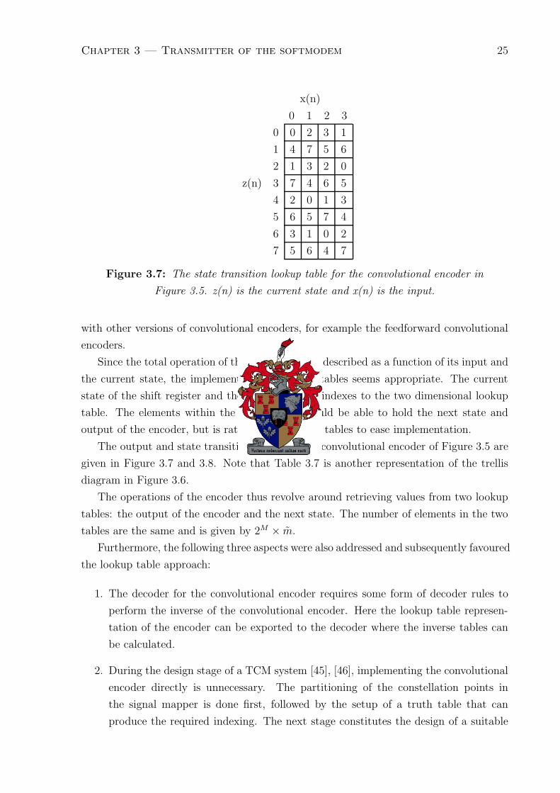
Figure 3.7: The state transition lookup table for the convolutional encoder in
Figure 3.5. z(n) is the current state and x(n) is the input.
with other versions of convolutional encoders, for example the feedforward convolutional
encoders.
Since the total operation of the encoder can be described as a function of its input and
the current state, the implementation of lookup tables seems appropriate. The current
state of the shift register and the input serves as indexes to the two dimensional lookup
table. The elements within the lookup table would be able to hold the next state and
output of the encoder, but is rather split into two tables to ease implementation.
The output and state transition tables for the convolutional encoder of Figure 3.5 are
given in Figure 3.7 and 3.8. Note that Table 3.7 is another representation of the trellis
diagram in Figure 3.6.
The operations of the encoder thus revolve around retrieving values from two lookup
tables: the output of the encoder and the next state. The number of elements in the two
tables are the same and is given by 2M × m.
Furthermore, the following three aspects were also addressed and subsequently favoured
the lookup table approach:
1. The decoder for the convolutional encoder requires some form of decoder rules to
perform the inverse of the convolutional encoder. Here the lookup table represen-
tation of the encoder can be exported to the decoder where the inverse tables can
be calculated.
2. During the design stage of a TCM system [45], [46], implementing the convolutional
encoder directly is unnecessary. The partitioning of the constellation points in
the signal mapper is done first, followed by the setup of a truth table that can
produce the required indexing. The next stage constitutes the design of a suitable

Chapter 3 — Transmitter of the softmodem 26
x(n)
0 1 2 3
0 0 2 4 6
1 1 3 5 7
2 0 2 4 6
z(n) 3 1 3 5 7
4 0 2 4 6
5 1 3 5 7
6 0 2 4 6
7 1 3 5 7
Figure 3.8: The output lookup table for the convolutional encoder in Figure 3.5. z(n) is
the current state and x(n) is the input.
Table 3.4: Convolutional encoder attributes
Attribute Default value Range Description
state table 1 4 0 0 0 0 matrix State transition table
output table 1 4 0 1 2 3 matrix Output table
convolutional encoder, but this would now be unnecessary since the truth table can
be loaded instead.
3. Since a non-linear convolutional encoder is used in this project, the only effective
method of implementing the convolutional encoder is as discussed above. By using
tables, it ignores any restrictions the operation of non-conventional encoders may
possess.
The convolutional encoder was tested with two sets of tables: the one given in V.32
bis as well as the tables of simple linear encoders used for illustrative purposes in the
literature where the output is also given. The output of these encoders was compared to
the tables and proved the correct working of the encoder.
The attributes assigned to the convolutional encoder is given in Table 3.4. The first
table holds the next state of the encoder and the other the output of the encoder. The
matrices are also not limited because an encoder can have any number of states or inputs.
3.4.3 Standalone binary convolutional encoder
The implementation as described above allows itself to be used as a standalone binary en-
coder. The output is made available for further digital processing and will not necessarily

Chapter 3 — Transmitter of the softmodem 27
d
1.141d
2d
2.83d
16 QAM Square
ConstellationSignal index:
XXXX
0XXX
0X1X0X0X
011X001X010X000X
Figure 3.9: Set partitioning of the 16-QAM signal as defined in V.32 bis
go to the signal mapper. If an input or output bitstream is required, the bit-to-integer
and integer-to-bit converters can be used.
3.4.4 Set partitioning
The concept of set partitioning is the second significant part of a TCM scheme. Set
partitioning is the successive division of a constellation into two subsets with each subset
having increasing smaller distances (di, i = 1− m) between the subset’s data points. The
partitioning is repeated m times until distance di is greater or equal than the desired
free distance , which is 2.83d for this modem. See Figure 3.9 for the set partitioning
for the 16 QAM, 9600 bps constellation defined in V.32 bis. The left branch is used to
show how each group is numbered, in the right hand branch the minimum free distance is
illustrated. The last group of constellations obtained by this process of subdividing (last
row in Figure 3.9) is the 2m subsets that are addressed by the output of the convolutional
encoder, y, in Figure 3.4.
The m − m uncoded bits shown in Figure 3.4 are used to choose a signal from the
selected subset. In the trellis diagram of Figure 3.6, each signal of the subsets become
associated with 2m−m parallel transitions to each state. In the special case of m = m
there is only one signal per subset and therefore there are no parallel transitions.

Chapter 3 — Transmitter of the softmodem 28
Lookup table
X
X
X
X
X
X
X
X
X
X
X
X
X
X
X
Xm
n
H(m,n)
Figure 3.10: Lookup table implementation for a two dimensional table
Table 3.5: The lookup table attribute
Attribute Default value Range Description
table - matrix Lookup table
From the description above, the mechanism of the TCM scheme becomes apparent.
Since only certain subsets are available at one time, the exclusion of other signal points
increases the Euclidean distances between the remaining signal points, allowing transmis-
sion of data over a more noisier channel. The signal mapper further signifies the transition
point between the digital operations and the analogue operations.
3.4.5 Implementation of the lookup table component
The signal mapper is a lookup table that associates an integer to a signal point in a con-
stellation. The uncoded and coded bits are used as separate indexes for a two dimensional
lookup table. The output of the convolutional encoder will be used as the index for the
row and the uncoded bits will be used as the index for the column. For this application,
the dimension of the lookup table is 2m × 2m−m.
The attribute assigned to the lookup table is presented in Table 3.5. Although the
lookup table is two dimensional, the lookup process will also work for an one dimensional
lookup table. The default entry is an empty matrix.
3.5 Pulse shape filtering
During transmission the transmitted signal undergoes various distortions due to a non-
ideal channel. A signal of this modem type will be subjected to one major distortion,
namely time dispersion. Time dispersion results from the deviation of the channel fre-
quency response from the ideal characteristics of constant amplitude and linear phase (or
constant delay).

Chapter 3 — Transmitter of the softmodem 29
The effect of the dispersion can be examined by evaluating the transmitted signal as
received by the receiver. After translating the passband signal to baseband, the received
signal can be written as [19]:
x(t) =∑k
akh(t − kT ) (3.4)
= an +∑k �=n
akh(t − kT ) (3.5)
where ak represents the symbol stemming from mapping, h(t) represents the impulse
response of the cascade connection of the shaping filter, the channel and additional filters.
T represents the symbol duration. Here it is assumed that the signal is sampled at the
correct instances and the effect of the transmission delay is ignored.
In Equation 3.5 the first term represents the correct symbol at time nT . The second
term is the result of the other symbols being dispersed by the channel over periods longer
than the symbol duration. This residual effect is know as intersymbol interference (ISI)
and it can have a unfavourable effect on the decision device at the receiver. Therefore, to
reduce the error rate at the receiver, the effect of ISI has to be reduced. This is achieved
by following the Nyquist criterion for distortionless baseband transmission [19], which
presents conditions for constructing band-limited filters that overcome ISI. A filter that
adheres to these conditions, is therefore necessary for a transmitter.
3.5.1 Raised cosine filter
To maximise spectral efficiency the filter should have a narrow bandwidth and a sharp
roll-off. The ideal filter with this characteristic and which satisfies the Nyquist criterion
is the rectangular low pass filter. This filter attenuates frequencies exceeding half the
symbol rate. Although an ideal solution, this filter is not realisable due to the sharp
transition that is required.
A more practical filter that satisfies the Nyquist criteria for eliminating ISI is the
raised cosine filter. The frequency response and impulse response is given by
P (f) =
⎧⎪⎪⎪⎨⎪⎪⎪⎩1
2B|f | < f1
14B
[1 + cos
(π(|f |−f1)2B−2f1
)]f1 ≤ |f | < 2B − f1
0 |f | ≥ 2B − f1
(3.6)
where B is half the symbol rate. The frequency f1 and bandwidth B are related by
α = 1 − f1
B(3.7)

Chapter 3 — Transmitter of the softmodem 30
0 0.2 0.4 0.6 0.8 1 1.2 1.4 1.6 1.8 20
0.2
0.4
0.6
0.8
1
Time (x 1/B)
Am
plitu
de (
x 1/
B)
Figure 3.11: Frequency response of the raised cosine filter for α = 0, 0.25 and 0.5
The parameter α is called the roll-off factor and determines the the amount of excess
bandwidth required. The value of α varies between 0 and 1 and corresponds with excess
bandwidth between 0% and 100%.
Figure 3.11 depicts the raised cosine filter and illustrates the relationship of α =
0, 0.2, 0.5. When α = 0, the spectrum is that of the ideal response for eliminating ISI.
The time response p(t) of the above filter is given by:
p(t) = sinc(2Bt)cos(2παBt)
1 − 16α2B2t2(3.8)
The ideal raised cosine filter has an infinite duration in the time domain. This is,
however, not practical and limiting the period of the impulse response introduces side-
lobes in the stop band of the frequency response. The order of the filter will thus determine
how much leakage there is in the stopband, which is where the spectral repetitions of the
interpolation process reside [35].

Chapter 3 — Transmitter of the softmodem 31
DAC
Time-continuous
filterh
AnalogImpulses
Analog Interpolated
SignalsInterpolants
Signal Samples
Resampleat t=kT
y(t) y(kT )x(mT (t)I
i
is )
Figure 3.12: Rate conversion with a time-continuous filter
3.5.2 Implementation of the interpolator
The function of the pulse-shaping filter is twofold. Besides filtering the incoming signal,
the pulse shaping filter has to interpolate from the symbol rate to the desired sampling
rate. Since the ratio of the symbol rate relative to the sampling rate should be able to
vary, the interpolator must make provision for this as well.
Returning to the concept of sample rate conversion mentioned briefly on p. 7, consider
Figure 3.12, which illustrates a fictitious hybrid analog/digital method of rate conversion.
The incoming digital signal is converted to analog impulses and applied to a time contin-
uous analogue filter with impulse response hI(t). The output of the filter is
y(t) =∑m
x(mTs)hI(t − mTs) (3.9)
The output is now resampled at time instants t = kTi where Ti is the required new
sampling period. The new samples are represented by
y(kTi) =∑m
x(mTs)hI(kTi − mTs) (3.10)
The above can be written in a more useful format by rearranging the indexing in the
equation. The following timing references are defined:
filter index:
i =
⌊kTi
Ts
⌋− m (3.11)
basepoint index:
mk =
⌊kTi
Ts
⌋(3.12)
fractional interval:
μk =kTi
Ts− mk (3.13)

Chapter 3 — Transmitter of the softmodem 32
FractionalInterval
BasepointIndex
INPUTSAMPLETIMES
OUTPUTSAMPLETIMES (k-1)T kT (k+1)T
(m -1)T
Time
μ T
i i i
k s
sk m Tsk (m +1)Tsk (m +2)Tsk m Tsk+1
Figure 3.13: Sample time relation
where 0 ≤ μk < 1 and �z� means the largest integer not exceeding z. Timing relations
are illustrated in Figure 3.13. The arguments in Equation 3.10 become m = mk − i and
(kTi − mTs) = (i − μk)Ts, and the interpolant is computed at time kTi = (mk + μk)Ts.
The Equation 3.10 now becomes
y(kTi) = y[(mk + μk)Ts] (3.14)
=I2∑
i=I1
x[(mk − i)Ts]hI [(i + μk)TS] (3.15)
Equation 3.15 is now written in terms of the following parameters: the filter index
i = I1 to I2, the basepoint index mk (which identifies the K = I2 − I1 + 1 signal samples
to be used for the kth interpolant), and the fractional interval μk(which identifies the K
filter coefficients to be employed for the kth interpolant).
Until now no assumption was made on the ratio of Ti
Ts, so this ratio could be irrational.
This means that μk could be irrational as well and it would change for each interpolant.
Consequently an infinite set of filter coefficients would be required for a infinite set of
values for μk.
In applications of sample rate conversion, such as the case is here, this ratio is typically
rational and takes on the form ID
where I and D takes on integer values. The values that
μk takes on becomes periodic, thus a finite set of filter coefficients is required with a set
for each value of μk. This set of coefficients would then be used periodically as well. The
number of sets are determined by the number of iterations Equation 3.16 must go through
before the same sequence is repeated.
NCO(m) =[NCO(m − 1) +
D
I
]modulo 1 (3.16)
Figure 3.14 illustrates the FIR filter structure used for periodically varying filter coef-
ficients [33]. In the figure, incoming samples are passed to a shift register at rate fs. The
shift register has length I which is the length of the impulse response of the filter given

Chapter 3 — Transmitter of the softmodem 33
Z -1
D/I
x ( mD/I )
h(0,k), k = 1, 2, ... , I-1
Z -1
D/I
x ( mD/I + 1)
h(1,k)
D/I
x ( mD/I - K + 1)
Z -1
D/I
x ( mD/I + 2)
h(2,k)
h(K-1,k)
x(n) y(m)
Rate = F Rate = I/D Fxx
Figure 3.14: Realisation of the sampling rate conversion by a rational factor I/D [33]
by Equation 3.15. Each delay element of the register is fed to a hold and sample device
that samples at rate Fy = (I/D)Fx. The K outputs of the hold and sample devices are
then multiplied with the periodically time-varying coefficients and the products summed
to yield y(k). The computations after the hold and sample devices are done at the output
sampling rate, Fy = (I/D)Fx.
For situations where the rational factor is such that a large set of filter coefficients are
required, this type of interpolation becomes inefficient in memory usage. A solution for
this rational factor would be to use polynomial based interpolation, where the interpo-
lated value is calculated from a polynomial that is a function of the fractional interval.
This method is used for symbol timing recovery (section 4.3), where the feedback loop de-
termines the correct sampling instance and the signal at that moment must be calculated.
This method is adaptive, but it can be modified to do constant sample rate conversion by
making the loop gain zero. It is a non-exact rate conversion scheme and will consequently
introduce distortion and deliver a poorer performance than the polyphase method.
Although raised cosine shaping filters are popular, they are not the only pulse shaping
filter that satisfies Nyquist criterion. The related root raised cosine filter is a popular
choice, but this filter needs to be used at the transmitter and receiver, so that the com-
bination forms the raised cosine pulse shaping filter. Other popular pulse-shapes include
the Gaussian pulse shaping filter, which is used in the mobile communications standards

Chapter 3 — Transmitter of the softmodem 34
Table 3.6: Interpolator attributes
Attribute Default value Range Description
input rate 1 - Sampling input
output rate 1 - Sampling output
filter rcosine rcosine Filter type
order 6 - Order of the filter
param 0.3 0-1 Parameter for filter
Re() DAC
jw nce
Pulse
Shape
Filter
s(n)
Figure 3.15: The quadrature modulator of the modem
where filters with small transition bands are required.
The attributes designated to the interpolator are shown in Table 3.6. For the input rate
and output rate attributes, the ratio is used during processing, so the actual rates can
be inserted or just the ratio, such as 1 and 5. The rest of the attributes define the
interpolation filter.
3.6 Quadrature modulator
The signal processing that has been done up to this point has all been done at baseband.
Transmitting the baseband signal may not be feasible since this will prohibit the channel
to be used by multiple users, or the frequency spectrum of the channel may not support
any signalling at DC, as is the case here.
The solution to this is to move the baseband signal to a higher frequency range in the
spectrum. This is achieved by multiplying the baseband signal with a carrier oscillator.
Figure 3.15 shows the latter portion of the transmitter of the modem, which includes the
quadrature modulator.
The complex input of the modulator comes from the pulse shaping filter. It is modu-
lated by multiplying the real/imaginary parts of the input with the in-phase/quadrature
components of a carrier phasor and then adding the resultant signals:
s(n) = �{a(n) ejωcn} (3.17)
= aI(n) cos[ ωcn] − aQ(n) sin[ ωcn] (3.18)

Chapter 3 — Transmitter of the softmodem 35
Table 3.7: Quadrature modulator attribute
Attribute Default value Range Description
carrier 0.3 0-0.5 Normalised carrier frequency
Since the quadrature modulator interacts directly with the DAC, the sampling rate
from the pulse-shape filter should be the same as the sampling rate of the DAC. The
DAC converts the sequence into an analogue signal for transmission over the channel.
Depending on the sensitivity of the DAC on the digital side, an additional gain may be
required between the quadrature modulator and DAC.
The attribute assigned to the quadrature modulator is shown in Table 3.7. It specifies
the normalised frequency of the carrier.
3.7 Conclusion
The transmitter was briefly described in the previous chapter together with a high level
block diagram. The block diagram in Figure 2.6 is repeated in Figure 3.16 but broken
down to include all functional parts. As mentioned, all functions had to be dedicated to
a block and kept as a separate entity, therefore the additions in the figure.
Regarding the order and type of processing performed by the components in this
implementation, it resembles the standard layout for a transmitter as adopted by other
implementations [4], [11] and [30]. There is little deviation from this unless extra digital
encoders are incorporated as may be required by other modem standards. The above is
in contrast to the layout of a receiver where the order of components are not fixed in a
sequence but may differ in a number of ways.
The rate at which each component operates is also shown in the figure. Although
it is fixed for each section in this case, it can be adapted for various components and
applications. In addition, attributes were assigned to each component to further expand
their capabilities.

Chapter 3 — Transmitter of the softmodem 36
Differential
Encoder
Signal
MappingConvolutional
Encoder
Data
Scrambler
ModulatorPulse-Shape
Filter
Input Bit
Stream
Analog
Bit to
integer
converter
DAC
0 - 4
22 3
fdNfd
fs
Figure 3.16: The transmitter as defined by V.32 bis
Chapter 4
Receiver of the softmodem
In the previous chapter the transmitter of the softmodem was discussed, firstly each
component in detail followed by a brief overview of the transmitter. This is continued for
the receiver starting with the basic components identified for the receiver in Chapter 2.
The functionality of the component is kept generic to broaden the capabilities of the
specific component. This idea is taken by evaluating the performance of some of these
components through unit tests to serve as guide for their implementation in a higher level
application. Just as for the transmitter, each component is assigned attributes through
which its parameters can change. The chapter concludes with a discussion of the overall
receiver.
4.1 Automatic gain control
The automatic gain control (AGC) is the first component to process the received signal.
At this stage a significant distortion of the signal may be present in the form of a very
attenuated signal. The purpose of the AGC is to adjust the amplitude of the signal to
a level that makes the amplified signal suitable for subsequent signal processing. This
adjustment should be slow enough as to not introduce AM distortion, which degrades
PAM-like signals [36].
Figure 4.1 shows a block diagram of the AGC system [5]. The incoming signal is
amplified by a gain that is proportional to the gain control signal produced by the loop.
Besides the signal being passed on to the output, it enters the loop for further processing
by the AGC.
The AGC loop starts with the energy detector block measuring the energy of the
signal over a predefined period. The measured energy is then subtracted from a reference
value to produce an error signal. The magnitude of the error is further compared to other
power levels to determine in which mode, or subsequently with which convergence speed,
the AGC should operate. The gain is then updated according to this mode. The details
37

Chapter 4 — Receiver of the softmodem 38
EnergydetectorExponential
integrator
Referencelevel
Modes selector
Input Output
g
-
+
ε
Gain error detector
Figure 4.1: Block diagram of the AGC
of the various parts are described below.
4.1.1 Gain error detector
The gain error detector determines by what gain the received signal differs from one
required for further processing by other precesses. This is done by calculating the energy
of the signal and then subtracting it from a reference energy level. The error produced is
given by the following equation:
ε(n) = x(n)2 − Eref (4.1)
where Eref is the reference energy level.
The corresponding gain error curve is shown in Figure 4.2 for a Eref = 1. Although the
curve can be assumed linear for small errors, the non-linearity becomes significant for very
small and very large signals. For very small signals the curve becomes bounded by −Eref ,
but this is not a problem since the exponential integrator that is used for adaptation of
the gain is well suited to handle negative errors, as will be seen. As for very large signals,
the curve grows quadratically, but is bounded by 1K
+Eref where K < 1 is the convergence
constant and Eref the reference energy level.
4.1.2 Mode selection
The signal level is now further examined to determine in which one of the slew or tracking
mode the AGC should operate. The slew modes becomes active when the error is high.
The convergence constant K is changed to a larger step size to speed up the convergence
to the optimum energy level. When the average energy reaches a level 3dB below and

Chapter 4 — Receiver of the softmodem 39
10−2
10−1
100
101
−1
0
1
2
3
4
5
6
7
8
9
10
Signal energy level
Err
or o
utpu
t
Figure 4.2: The gain error detector curve for energy levels ranging from 0.001 to 10

Chapter 4 — Receiver of the softmodem 40
Tracking mode
Tracking mode
Slewmode
Slewmode
Inputsignallevel
High amplitude levelLow amplitude level
Referencelevel
Figure 4.3: AGC operating modes
above the reference level, the AGC enters the tracking mode. Here the step size is reduced
to get a slower response and consequently a more accurate tracking of the signal. These
concepts are illustrated in Figure 4.3
The convergence constant is updated if required and is multiplied with the error. The
gain of the AGC is updated by the following exponential integrator loop:
gn+1 = gn × (1 − Kε) (4.2)
For the gain to remain positive, Kε < 1 must be adhered to. This is why the maximum
signal is limited to 1K
+ Eref . When the AGC is in slew-mode, K = 0.075 for the entire
time it is in this mode. It is equivalent to reaching 60dB in 100 samples.
4.1.3 Signal presence detection
The signal presence detector detects whether a signal is present on the channel. It uses
a low-pass filter that measures the average energy over a predefined period. Since linear
phase is not a requirement for this measure, the single-pole Butterworth filter is used to
calculate the average energy. The cutoff frequency was made a function of the number of
samples averaged over, so that the number of samples can be defined beforehand.
With the average energy calculated, it can be tested against a threshold level that
determines whether a signal is present or not. If the signal level exceed this level, the
AGC sends samples on to the following component. When below this level, all samples
are disregarded. To make the detection effective, the number of samples has to span a
few symbol periods. Further, due to its averaging effect, the detector also features in the
detection of the modes as discussed above.
4.1.4 Evaluation of the AGC
The evaluation of the AGC comprises of noting the response of the gain element through
the stages of operation as illustrated in Figure 4.3. The test signal consisted of a QAM

Chapter 4 — Receiver of the softmodem 41
0 50 100 150 200 250 300 350 400 450 50010
0
101
102
103
AG
C g
ain
samples
Tracking Mode Slew Mode
Figure 4.4: Response of the AGC to a low energy signal
signal that was gradually increased in amplitude until it was higher than the threshold
level. From here on the AGC would adapt the energy level to the appropriate level.
Figure 4.4 shows the adaptation of the signal level through various stages. At first
the gain remains at 1, which is the default value of the gain. As soon as the test signal
reaches the threshold level, the AGC switches to the slew mode where the convergence
is made fast. When the gain nearly reaches the correct level, the AGC changes to the
tracking mode, which is evident with the slower response.
The figure also shows that the gain does not remain constant. The gain error is
driven by a moving averaging filter thus the variance in the input introduces noise in the
feedback loop. Should this become problematic, feedback from a decision device can be
incorporated.
The attributes assigned to the AGC is shown in Table 4.1. The threshold and duration
attributes are used to determine whether a signal is present on the channel. Stepsize is
the convergence constant K as mentioned above. The reference attribute stipulates the
energy level of the signal at the output of the AGC.

Chapter 4 — Receiver of the softmodem 42
Table 4.1: Automatic gain control attributes
Attribute Default value Range Description
threshold 0.00001 - Signal presence level
duration 100 - Signal presence duration
stepsize 0.01 0-1 Stepsize for tracking mode
reference 1 - Reference energy level
4.2 Quadrature demodulator
The signal received from the AGC contains a passband signal that is centered around
the carrier frequency. The baseband signal at the transmitter was mixed with quadrature
carriers to move the complex baseband signal to a higher frequncy range. This had to be
done because the characteristics of the channel did not allow the baseband signal to be
transmitted. The purpose of the quadrature demodulator is thus to convert the passband
signal back into a baseband signal for further baseband related signal processing.
For a mathematical description of the process, assume the signal transmitted and
received is
s(n) = 2a(n)cos[ωcn + θ(n)] (4.3)
with all of the channel’s effects ignored. The signal is demodulated by the multiplying it
with a complex phasor, which gives
y(n) = s(n)e−jωcn (4.4)
= 2a(n) cos[ωcn + θ(n)] × [cos(ωcn) − j sin(ωcn)] (4.5)
= a(n) cos[θ(n)] + ja(n) sin[θ(n)] (4.6)
+a(n) cos[2ωcn + θ(n)] − ja(n) sin[2ωcn + θ(n)] (4.7)
After the low pass filter removes the frequencies at 2ωc, which is represented by the two
last terms in Equation 4.7, the output of the filter produces
yLPF(n) = a(n)ejθ(n) (4.8)
which is the complex baseband signal. Figure 4.5 shows the components involved to
achieve this. The input signal is multiplied with a complex phasor and then passed
through a lowpass filter, which is used to eliminate the frequency components generated
at twice the carrier frequency.
A further requirement of the filter is that it should not attenuate any frequency com-
ponents of the baseband signal while trying to remove the double frequency components.

Chapter 4 — Receiver of the softmodem 43
Image
Rejection
Filter
jw nce
Input
from
AGC
Complex
Baseband
Signal
Figure 4.5: Quadrature demodulator and the image rejection filter
Table 4.2: Quadrature demodulator attribute
Attribute Default value Range Description
carrier 0.3 0-0.5 Normalised carrier frequency
It is possible that in a prior mixing stage the oscillator was not working at the correct fre-
quency and as a result, mixed the signal to a frequency with a slight offset. The frequency
offset produces a baseband signal that is centered at Δf , the offset of the inaccurate mixer.
The filter must accomodate these situations as well.
4.2.1 Implementation of the demodulator
The implementation of the demodulator is divided into two components: the mixer and the
filter. This is done because quadrature demodulation of a complex passband signal does
not involve the filter as no double frequency components are generated when multiplied
with a complex phasor. For a real passband signal, the filter is required.
The quadrature demodulator consists of a multiplier which multiplies the complex
phasor with the incoming signal. The complex phasor is made up of a real and an imagi-
nary component that takes on the values the cosine and sine functions for an increasing
or decreasing angle. The attribute assigned to the quadrature demodulator is given in
Table 4.2. The carrier attribute is used to specify the carrier frequency relative to the
sampling rate.
The filter uses a Direct Form I structure to do the filtering. Although the transposed
Direct Form II seemed the more obvious choice due to its efficient use of memory, the first
structure has the advantage of storing past output values. This gives the filter the added
ability to function as a delay buffer.
The attributes assigned to the filter is given in Table 4.3. The num and den attributes
allow the numerator and denominator to be loaded. The alternative to this is to specify the
filter type and associated parameters. Cutoff, window and order specifies the conditions
for a low pass filter of any order combined with a windowing function.

Chapter 4 — Receiver of the softmodem 44
Table 4.3: Filter attributes
Attribute Default value Range Description
num 0.5 0.5 - Numerator
den 1 - Denominator
cutoff 0.1 0-1 Normalised cutoff frequency
window hamming hamming Window function
order 6 1-100 Order of filter
4.3 Symbol timing recovery
In a synchronous communication system, it is essential that the receiver obtain accurate
timing information indicating the proper time instance to operate the sampling device
which processes the (complex) baseband signal. The problem is especially acute in multi-
level signals with limited bandwidth, and the timing error must be held to a small fraction
of a symbol period for satisfactory performance.
The symbol synchroniser is an all-digital symbol synchroniser, unlike that of the first
digital modems that used the advance and retard capabilities of the ADC to retrieve the
signals at the correct time instances [7], [28]. The timing information is extracted from
the data signal itself and this is used to calculate the sample at the correct instance from
the adjacent samples retrieved from an ADC with a free-running oscillator.
The symbol timing recovery clock’s purpose is twofold: it converts the incoming signal
from a higher sampling rate to a lower one and at the same time does symbol timing
recovery by means of a closed feedback loop. These two functions are distinct and can
be used separately if required. In some systems, for example, sample rate changes can
be very large, as high as 500. Such requirements lead to large-order and high-rate digital
filters, which must be done by more efficient sample rate conversion algorithms such as
Cascaded Integrator Comb filters [35]. The symbol synchroniser can then operate with
an input and output rate that are closer to each other, thus performing only fractional
delay on the input.
The functional components of the symbol synchroniser are shown in Figure 4.6. The
input is fed to the interpolator which calculates the sample at the correct time instance,
from information attained by the feedback loop. The sampled forms the output of the
synchroniser and serves as input to the timing error detector as well. The generated error
signal is then sent through a loop filter from where it adjusts the phase of a reference
clock, which is tuned to the symbol frequency. These components are described in detail
in the following paragraphs.

Chapter 4 — Receiver of the softmodem 45
Timing Error
Detector
Loop
Filter
Interpolator
Output
Input
Figure 4.6: Block diagram of the symbol synchroniser
4.3.1 Polynomial-based interpolation filter
In section 3.5 the fundamental equation for interpolation was described by:
y(kTi) = y[(mk + μk)Ts] (4.9)
=I2∑
i=I1
x[(mk − i)Ts]hI [(i + μk)Ts] (4.10)
where x(mTs) is a sequence of samples taken at intervals Ts and hI(t) is the impulse
response of a fictitious, time-continuous interpolating filter. The digital implementation
delivers samples y(n) at adjustable intervals Ti.
The parameters are the filter index i = I1 to I2, the basepoint index, mk (which
identifies the I = I2 − I1 + 1 signal samples to be used for the kth interpolant), and the
fractional interval μk (which identifies the I filter coefficients to be employed for the kth
interpolant).
A polynomial-based filter is a filter of which the impulse response hI(t) is a (piecewise)
polynomial in t, or as will be used here, in μk. Associated with every polynomial filter
is a time-continuous approximating polynomial pk(t) which approximates the value of
y(t) at instance t = kTi. The interpolating filter of Equation 4.10 computes samples
y(kTi) = pk(kTi) of this polynomial. The approximate polynomial is also different for
each value of I when the interpolant is calculated.
A popular choice for coefficients of a interpolating polynomial is coefficients derived
from Lagrange’s interpolation formula [47], [12]. The formula provides the equation of
a polynomial of degree n in t, or equivalently μk, with an impulse response duration of
n + 1 samples. Each interval between base points has a unique piecewise formula and the
resulting Lagrange coefficients constitute the interpolation filter response hI(t).
Polynomials of odd degree deliver a unique interpolant and for practical purposes
only two will be considered: the first (linear) and third (cubic) degree polynomials. The

Chapter 4 — Receiver of the softmodem 46
−2 −1.5 −1 −0.5 0 0.5 1 1.5 2−0.2
0
0.2
0.4
0.6
0.8
1
1.2
time (x 1/T)
Am
plitu
de
Figure 4.7: Impulse response of the linear and cubic interpolating polynomial

Chapter 4 — Receiver of the softmodem 47
time-continuous impulse response hI(t) of the polynomials are shown in Figure 4.7. The
impulse response of the linear interpolator is a triangle with hI(0) = 1 and a base width
of 2Ts. In the case of the cubic interpolator, each segment of duration Ts is a cubic
polynomial, making the entire impulse response a piecewise polynomial. Each of the
impulse responses is symmetric about t = 0, which is required for linear phase filtering.
The frequency responses of these impulse responses have nulls at harmonics of the
sampling frequency, where the images of the input is situated. The cubic interpolator
gives a wider band of attenuation than the linear interpolator, as well as a wider and
flatter passband. Thus signals sampled close to two samples per symbol will deliver
better interpolants with a cubic interpolator than the linear interpolator. However, for
higher sampling ratios, the simpler operation of a linear interpolater will be sufficient.
Farrow filter structure
The Farrow structure [13] provides a convenient way to implement these polynomial-based
filters. Although a filter characteristic underlies any interpolator, the coefficients of the
filter do not have to be visible in the filter structure. Here the purpose of the filter is to
produce interpolants, so other means of calculating the interpolant can be employed.
Let the impulse response of the interpolating filter be piecewise polynomial in each Ts
segment, i = I1 to I2:
hI(t) = hI [(i + μk)Ts] =N∑
l=0
vl(i)μlk (4.11)
Substituting 4.11 into 4.10 gives
y(k) =I2∑
i=I1
x(mk − i)N∑
l=0
vl(i)μkl (4.12)
=N∑
l=0
μlk
I2∑i=I1
vl(i)x(mk − i) (4.13)
=N∑
l=0
μlkb(l), b(l) =
I2∑i=I1
vl(i)x(mk − i) (4.14)
The equation shows that the coefficients vl(i) are constant numbers and are determined
only by the impulse response of the interpolation filter. The μk fractional indicator is thus
independent of the filter. Figure 4.8 shows the implementation of Equation 4.14. The
blocks represent the transversal filter computing b(l).
The Farrow coefficients are not limited to the Lagrange coefficients, as a Farrow de-
composition is possible for any polynomial-based filter. Further, research into Farrow
coefficients also delivered methods that calculate optimised coefficients that suit particu-
lar conditions, such as those described in [44], [43] which minimise the MSE for various
parameters such as the symbol decision instants. The Lagrange coefficients will be used

Chapter 4 — Receiver of the softmodem 48
b(3) b(2) b(1) b(0)
{v (i)} {v (i)} {v (i)} {v (i)}013 2
μk
Input
Output
Figure 4.8: Farrow structure for a cubic interpolator
Table 4.4: Farrow coefficients for a cubic interpolator
i v = 0 v = 1 v = 2 v = 3
−2 0 −16
0 16
−1 0 1 12
−12
0 1 −12
−1 12
1 0 −13
12
−16
as the default condition as it can cater for numerous conditions. Alternative coefficients
can be set if required.
The output of the symbol synchroniser is thus a reconstruction of the input sampled
at the symbol instances. With the addition of some code the STR can be programmed
to produce a signal sampled at an integer multiple of the symbol rate. This allows for
more accurate signal processing in subsequent components if required, such as a frac-
tionally spaced equaliser. With multiple samples per symbol, extra information needs to
accompany the samples to show its time relation to the symbol instance.
4.3.2 Timing error detector
The function of the Timing Error Detector (TED) is to produce an error signal which
indicates the time difference between the symbol instance in the received signal and the
symbol instance in a reference clock. There are numerous techniques of detecting the
correct instances [29], but the detector deemed the most suitable for this application is
the Gardner detector [17]. This TED is intended for synchronous baseband signals and
although it was originally designed for BPSK and QPSK signals, it has also found use in
M-ary QAM signals [10].
The detector has several advantages above others. It was derived from the square law
rectifier and thus inherits some of its features. The advantages of the Gardner detector

Chapter 4 — Receiver of the softmodem 49
are:
1. it requires only two samples per symbol;
2. it is not data-aided;
3. it recovers symbol timing without depending on carrier lock;
4. one of the samples used coincides with the sampling instance, thus no extra inter-
polation is required.
The Gardner detector estimates the timing error by
y(n) = �{x(n − 1) (x(n) − x(n − 2))} (4.15)
= xI(n − 1) (xI(n) − xI(n − 2))
+xQ(n − 1) (xQ(n) − xQ(n − 2)) (4.16)
where x(n) and x(n − 2) are the current and previous complex samples at the symbol
instances, and x(n − 1) the sample midway between them.
Note that the error signal produced by Equation 4.16 is proportional to the amplitude
of the signal and is not necessarily proportional to the actual error. Therefore a constraint
is put on the input that proper normalisation has to occur prior to this stage. This task
is left to the AGC to adjust the incoming signal to the correct power level.
The output of the Gardner detector is shown in Figure 4.9. At the origin, the detector
shows a linear relationship between the input and output for input values between −0.25 T
and +0.25 T , with the sign of the error still being correct outside these points.
The figure also shows the sinusoidal curves for various roll off factors of the raised
cosine pulse-shaping filter. The height of sinusoid is proportional to the energy in the
excess bandwidth of the pulse shaping filter, so the narrower the filter, the smaller the gain.
Too little excess bandwidth would thus deliver a poor performance. A large attenuation
at the cutoff frequency caused by a channel will also have the same effect, so this TED
would not be suitable for channels with nulls at half the symbol frequency on either side
of the carrier. This feature is inherent to quadratic TED.
Simulations have also shown that the curves are independent of the constellation layout
and size, provided that the occurrence of each signal point in the constellation is assumed
equiprobable.
4.3.3 Loop filter
In most systems, the timing instances and the frequency of the symbols are not known
at the receiver [16]. Phase steps occur due to unknown initial conditions and frequency
offsets are caused by the difference in the sampling rate at the transmitter and receiver.

Chapter 4 — Receiver of the softmodem 50
−0.5 −0.4 −0.3 −0.2 −0.1 0 0.1 0.2 0.3 0.4 0.5
−0.2
−0.1
0
0.1
0.2
0.3
Timing offset (x 1/T)
Det
ecto
r ou
tput
α = 0.2
α = 0.5
Figure 4.9: The S-curve for various values of the roll off factor
Chapter 4 — Receiver of the softmodem 51
It is the function of the loop filter to compensate for these phase and frequency errors.
An appropriate loop filter is a proportional plus integral (PI) compensator [15], given by
the following:
y(n) = KP x(n) + KI{x(n) + e(n − 1)} (4.17)
where e(n − 1) is the previous output of the integral portion of the compensator. The
subsequent closed loop transfer function is a stable second degree transfer function that
can track out phase and frequency offsets.
The loop filter was also used in modelling the symbol synchroniser, with the purpose
to characterise its time response in terms of an attribute that would make sense to a
developer. Here the open loop bandwidth was made the variable and also an attribute for
the component. The open loop bandwidth determines how fast the synchroniser attains
lock.
4.3.4 Evaluation of the symbol synchroniser
The symbol synchroniser was evaluated with a signal where the symbol instances had
constant time and frequency offsets. The test signal comprised of an initialisation period
which was used to eliminate transient effects of initial values followed by a sudden jump
in phase (time) and frequency.
The phase jump was created by deleting some samples from the signal. The ratio of
this number relative to the number of samples per symbol constituted the instantaneous
phase error and the deleted samples also had to follow directly after a symbol instance.
The phase error is given by:
θe = M × fd
fs
(4.18)
where M is the number of deleted samples and fd
fsis the ratio of the symbol data rate to
the sample rate.
The frequency offset was created by interpolating the test signal with a lower ratio
than the ratio expected to be correct by the symbol synchroniser. The frequency offset
ratio is given by
ωe =f ′
d − fd
fs(4.19)
where f ′d is the adjusted symbol rate of the test signal.
The evaluation used a test signal that had a phase error of 0.25T , followed by one
with a frequency error (0.05T per symbol). For the second signal a faster response time
was used at the synchroniser to compensate for the frequency error. Figure 4.10 depicts
the typical response of the symbol synchroniser to the test signal.

Chapter 4 — Receiver of the softmodem 52
0 100 200 300 400 500 600 700 800 900 1000−2
−1.5
−1
−0.5
0
0.5
1
1.5
2
2.5
Err
or s
igna
l
samples
Figure 4.10: Typical response of the symbol synchroniser

Chapter 4 — Receiver of the softmodem 53
Table 4.5: Symbol synchroniser
Attribute Default value Range Description
bandwidth 0.001 0-1 Normalised loop bandwidth
farrow cubic cubic/matrix Farrow coefficients
input rate 8000 - Input rate
output rate 2400 - Output rate
Θ = φ + ωt
Real
Imag
Figure 4.11: Rotated 16-QAM constellation due to unknown initial phase and
frequency offset
The figure shows that the average error converges to zero and thus the synchroniser
achieved lock on the signal. As mentioned the open loop bandwidth was adjusted to
make its response faster for the second signal because the synchroniser did not lock with
the same open loop bandwidth of the first signal. The spikes in the error signal are a
byproduct of the TED.
The attributes allocated to the synchroniser is given in Table 4.5. Since the symbol
synchroniser in concept performs the inverse of the interpolator, the attributes of the
synchroniser were kept similar to those of the interpolator. The bandwidth attribute
determines the openloop bandwidth of the closed loop. The farrow attribute stipulates
what coefficients to use. The cubic are set hardwired options, but other can be loaded
too in the form of a matrix.
4.4 Carrier synchronisation
The coherent reception of a digitally modulated signal requires that the receiver’s carrier
be synchronous with that of the transmitter. However, carrier phase offsets are introduced
by inaccurate system parameters and for the receiver to eliminate this error, it must
perform carrier synchronisation on the signal [16].
Figure 4.11 shows the effect of a carrier phase offset on a 16-QAM constellation. The
Chapter 4 — Receiver of the softmodem 54
constellation is rotated by an angle which is a function of the following:
constant phase error This error is the difference Δφ between the initial phase of the
transmitter’s carrier and the reference carrier of the receiver and is due to the
starting phase of the transmitter not being known at the receiver.
A′(k) = A(k)ejΔφ (4.20)
constant frequency error Frequency error Δω is caused during the up/down conver-
sion process where the signal is moved between baseband and passband by means
of an inaccurate oscillator at the receiver or the transmitter.
A′(k) = A(k)ejΔωk (4.21)
Conventional carrier synchronisers for simple M-PSK constellations depended on phase
symmetry to achieve synchronisation [34], [18]. The phase detector in these synchronisers
used a non-linearity that produced harmonics of the carrier frequency and then a PLL
would lock onto this frequency, which would be M times the carrier frequency for a M-PSK
constellation.
In M-QAM constellations the points are not just restricted to certain phase intervals,
but may vary in the distance from the origin as well. The position of these points are
typically at regular intervals from the two axes and forms a rectangular grid. The receiver
must now lock on these unique positions before the correct constellation point could be
chosen. The symmetry also eases the task of the decision device. Since there is limited
information in the constellation layout that can be exploited, the carrier synchroniser
must incorporate some sort of decision feedback PLL [32]. The DFPLL may be used with
any two dimensional constellation, irrespective of the phase and amplitude relationship
among the points.
Figure 4.12 shows a block diagram of a typical carrier synchroniser. The phase of the
input is compared to that of the reference carrier by means of the phase error detector.
The error signal for the loop is produced by the difference in the comparision. The error
is then sent through a loop filter from where it adjusts the phase of the reference carrier.
These elements are described in the following paragraphs.
4.4.1 Phase rotator
The phase rotator multiplies the input of the carrier synchroniser with a reference phasor.
The effect is that the complex input is rotated by a certain angle. The reference phasor
is continuously adapting to neutralise any phase offsets, driving the error to zero. The
multiplication is given by
ry(n) = rx(n)ejθref(n) (4.22)

Chapter 4 — Receiver of the softmodem 55
Phase Error
Detector
Loop
Filter
Reference
Phasor
e jT (n)
Output
Input
Phase Rotator
Figure 4.12: Block diagram of the carrier synchroniser
The trigonometry functions used to calculate the reference phasor are calculated here,
but can also be looked up in a table. The accuracy of these will determine the amount of
self noise the loop will introduce.
4.4.2 Phase error detector
The phase detector measures the difference in phase between the received signal point and
the correct signal point. This is used to drive the reference phasor to rotate the incoming
complex signal by the right amount.
Assume the received signal and the correct signal is given by rx and rd, then the phase
error is calculated as follows:
re = rxr∗d (4.23)
= |rx||rd|ejθx−θd (4.24)
= |rx||rd|ejθe (4.25)
The phase error is given in the angle of re. The angle is extracted by assuming tan( ba) ≈ b
a
where re = a + jb. The angle is thus calculated by the following:
θe =
⎧⎪⎪⎪⎨⎪⎪⎪⎩π2− a
b−π
2< θ < π
4ba
π4
< θ < π4
−π2− a
b−π
2< θ < π
4
(4.26)
To determine in which region the angle is found, the values of a and b are compared with
each other to see in which angle sector it lies.
Equation 4.26 is depicted in Figure 4.13 as a monotonically running curve except for
discontinuities at θe = ±π4. These discontinuities occur at the angle where the method of

Chapter 4 — Receiver of the softmodem 56
−0.5 −0.4 −0.3 −0.2 −0.1 0 0.1 0.2 0.3 0.4 0.5−0.5
−0.4
−0.3
−0.2
−0.1
0
0.1
0.2
0.3
0.4
0.5
Phase offset
Det
ecto
r ou
tput
Implemented DetectorIdeal Detector
Figure 4.13: Phase error detector curve
calculating the phase error changes. This resulting inaccurate phase error will, however,
not have a significant influence on the performance of the synchroniser as it occurs at a
large phase error and will not be applicable in constellations where the angle between the
data points is more than π2.
The accurate working of the carrier synchroniser is necessary for a modem, especially
one with large constellations. But its purpose should extend beyond this in a modem,
such as locking onto a single carrier during the handshaking period. No symbol data is
embedded in the signal to estimate the phase error, but a feature of the single carrier
that can be used, is that all of the samples are limited to one dimension in the complex
baseband signal space. Since all samples lie in one dimension, all have the same phase
offset relative to the axis and this can be used for the phase error calculation. This puts
no restriction on what the sampling rate of the signal can be. The above also applies to
other one dimensional signals, such as ASK and BPSK.
4.4.3 Loop filter
In most systems, the initial phase and the possible offset in the carrier’s frequency are not
known at the receiver. Phase steps occur due to unknown initial conditions and frequency
offsets are caused by the inaccurate oscillators used by mixers at the transmitter and
receiver. It is the function of the loop filter to compensate for these phase and frequency
errors. An appropriate loop filter is a proportional plus integral (PI) compensator [15],
given by the following:
y(n) = KP x(n) + KI{x(n) + e(n − 1)} (4.27)

Chapter 4 — Receiver of the softmodem 57
0 100 200 300 400 500 600−0.4
−0.2
0
0.2
0.4
0.6
0.8
1
Pha
se E
rror
in R
adia
ns
samples
B = 0.01 ω c
B = 0.001 ω c
Figure 4.14: Phase error signal achieving lock
where e(n − 1) is the previous output of the integral portion of the compensator. The
subsequent closed loop transfer function is a stable second degree transfer function that
can track out phase and frequency offsets.
Just as for the symbol synchroniser, the carrier recovery algorithm was modelled and
made a function of the open loop bandwidth of the feedback loop.
4.4.4 Evaluation of the carrier synchroniser
The carrier synchroniser was evaluated with two signals that consisted of BPSK constel-
lation points rotated by an angle that would represent the phase and frequency offsets.
The test signal comprised of an initialisation period which was used to eliminate transient
effects of initial values followed by a sudden jump in phase and frequency.
The phase and frequency jump was created by rotating the constellation point through
A(n) = A(n)ej(θ+ωen) (4.28)
where θ is the angle of the phase jump and ωe the constant frequency jump.
The two test signals had a frequency offset of 0.01ωc and 0.001ωc and both had the
same phase jump of π3. Figure 4.14 depicts the response of the carrier synchroniser to the

Chapter 4 — Receiver of the softmodem 58
Table 4.6: Carrier synchroniser attributes
Attribute Default value Range Description
bandwidth 0.01 0-0.5 Normalised loop bandwidth
constel real real/square Constellation form
feedback no yes/no Feedback of correct point
Adaptivefilter
Decisiondevice
Trainingsequence
Training mode
Data mode
x(n)
e(n)
y(n)
d(n)
+
-
Figure 4.15: Adaptive equaliser
two test signals. The open loop bandwidth was made B = 0.01ωc and B = 0.001ωc for
the two signals.
The figure shows that the error signal converges to zero for both cases and thus the
synchroniser achieved lock on both signals. As mentioned the open loop bandwidth was
adjusted to make its response faster for the second signal because the synchroniser did
not lock with the same parameters as the first signal.
The attributes allocated to the carrier synchroniser is given in Table 4.6. The nor-
malised open loop bandwidth is given by bandwidth. The next two attributes specify
which reference for the correct signal is to be used: constel for internal calculation by
referring to a real or square layout, or from a feedback path.
4.5 Adaptive equalisation
Although pulse-shaping (Section 3.5) was performed at the transmitter to combat the
dispersive effect on the transmitted signal, the channel still introduced some degree of
distortion as well as added Gaussian noise. When the constellation points are increased,
the distance between signal points decreases for the same transmitted power. It is thus
very important for the adaptive equaliser to compensate for the amplitude and phase
distortion in order to clean up the received samples.
Chapter 4 — Receiver of the softmodem 59
The adaptive equaliser consists of two components: a transversal filter that performs
the convolution operation on the input and an adaptive algorithm that adjusts the coef-
ficients of the filter to improve its performance. These two parts are illustrated in Figure
4.15.
The input signal, xn, is the received signal distorted by the channel plus added noise.
This signal is the sent through the adaptive filter to produce the equalised signal, yn. The
decision device is used to estimate the received symbol from yn. This symbol is depicted
by de. The error signal, en, is the equalised signal subtracted form the estimated symbol
and is used the adaptive algorithm to adjust the coefficients.
The input sequence is convolved with the impulse response of the equaliser to combat
the distortion inflicted by the channel. If the equaliser were the inverse of the channel
response, then the combined equaliser and channel system would produce an impulse
response with a one at the main sample and zeros at the other. This combination would
minimise ISI, even with a channel whose characteristics vary over time.
4.5.1 Least mean-square equaliser
The least mean-square (LMS ) equaliser [20] is a simple and very robust adaptive algo-
rithm, in the sense that the coefficients are chosen to minimise the Mean Square Error
(MSE) - the sum of squares of ISI and noise contributions at the output of the equaliser.
The LMS equaliser therefore maximises the signal-to-distortion and noise ratio at the
equaliser output within the constraints of the equaliser length and delay.
The update algorithm for the coefficients is given by:
wk(n + 1) = wk(n) + μe∗nxn−k k = 0, ..., M (4.29)
where wk(n) is the estimate of the kth filter coefficient before adaptation, wk(n + 1) is
the estimate of the kth filter coefficient after adaption, e∗n is the complex conjugate of the
estimated error at the nth iteration, xn−k is the value of the tap input applied to the kth
filter coefficient at the nth iteration and μ is the adaptation constant.
The error estimate, en, is defined by
en = dn −M∑
k=0
w ∗k (n)xn−k (4.30)
where the first term is the output of the decision device and the second is the filter output,
which gives an estimate of dn. The whole LMS algorithm is described in Equation 4.29
and 4.30.
4.5.2 Step-size parameter
The LMS algorithm forms a closed loop feedback system where the value of the adaptation
constant, μ, determines the convergent properties of the loop. The bigger the value of μ,

Chapter 4 — Receiver of the softmodem 60
Table 4.7: LMS attributes
Attribute Default value Range Description
order 15 - Order of the filter
stepsize 0.01 - Adaptation constant
coeff 0 - Coefficient of filter
buffer 0 - Buffer for input samples
delay 0 - Delay between input/feedback input
the faster it converges, but the larger the final state error will be. When μ is too small,
the final error state is small, but convergence takes long to occur. To assure convergence,
the following applies:
0 < μ <2
G∑M
x2(4.31)
where x is the input to the LMS filter and G the gain in the feedback loop. The average
tap input power is a function of the input to the receiver and all the components up to the
adaptive equaliser that amplifies the signal in their implementation. If these gains and
the gains in the feedback loop are known, then the adaptation constant can be adjusted
accordingly.
4.5.3 Evaluation of the LMS equaliser
The LMS algorithm was tested for various channels for which it was suited and it converged
for all of them. The evaluation of the standard LMS equaliser is a standard analysis in
literature descibing the algorithm so the results produced were not shown. The fact that
it converged proved that its implementation was correct.
The attributes of the LMS algorithm are depicted in Table 4.7. The order and stepsize
attributes are standard parameters for the LMS algorithm. The attributes coeff and buffer
are used to load or retrieve the input and coefficient buffers of the algorithm. Delay is
used to set the delay between the algorithm input and feedback input. This is required
because the coefficient update algorithm requires direct feedback, which is not possible
when other components are linked in the feedback path.
4.6 Viterbi decoding
The purpose of the Viterbi decoder is to reconstruct the transmitter’s trellis path from
the channel corrupted data using a maximum likelihood approach. It compares every

Chapter 4 — Receiver of the softmodem 61
possible coded sequence over a certain time period to the received sequence and the path
with the largest likelihood is then selected. The data bits that correspond to this path
forms the output of the decoder.
The flow diagram for the Viterbi decoder is shown in Figure 4.16. All the sections
shown in the diagram are discussed in the subsequent paragraphs.
4.6.1 Initialisation
A large portion of the Viterbi algorithm uses multiple lookup tables to perform the de-
coding. These tables were implemented in such a way as to reduce the computational
load on the processor. The following describes the tables that are used:
• The constellation-table holds the complex signal points of the constellation used
to calculate the Euclidean distances.
• State table and output table hold the decoder map that forms the core of the
Viterbi algorithm. These tables are the inverse of the tables in Figures 3.7 and 3.8,
which defined the working of the convolutional encoder.
• The state history-table holds the various possible state transitions over a certain
predefined period.
• The subset and subsetpoint tables hold the coded and uncoded output of each
associated state in the state history table.
• Acc dist holds the accumulated distance associated with each state transition se-
quence.
The first three tables are unique for each trellis codec and must be initialised prior to
execution of the Viterbi algorithm. The first element in the accumulated distance table
is set to zero while the others are set to a bigger value to ensure that the first path starts
at state zero. The rest of the tables are all initialised to zero.
It should be mentioned that during initialisation, the corresponding tables of the
convolutional encoder are loaded in state table and output table. These tables are
then reconstructed to form the inverse of the tables loaded. Where the encoder table
looked like
T[current state][encoder input] = next state; subset
It is transformed to take the following form to do the processing:
T[current state][subset] = previous state; encoder input

Chapter 4 — Receiver of the softmodem 62
Start
Initialise
Read input data
Compute smallest distance from received symbol in each subset.
Compute accumulateddistances associated with
each state transitions.
Trace back from current state.Get subset at earliest state
Decode subset.Output corresponding
data
End of inputno
yes
Stop
Find minimum accumulated distance. Select
corresponding state
Figure 4.16: Flow diagram for the Viterbi decoder
Chapter 4 — Receiver of the softmodem 63
4.6.2 Minimum distance calculation
The first processing involved in the Viterbi algorithm is the calculation of the Euclidean
distance between the received signal point and the correct signal point. The Euclidean
distance metric is defined as
dEuclidean = |x − a|2 (4.32)
where x is the complex input and a is the correct complex subset point The Euclidean
distance between the received signal and the constellation point is calculated for each of
the points in a subset. The point associated with the smallest distance is then stored in
the subset table indexed under the specific subset number together with the distance.
This whole process is repeated for each of the remaining subsets. All of the signal points
are contained in the constellation-table.
Depending on the constellation size, this part of the Viterbi algorithm can put a very
large computational strain on the processor. The calculations can however be reduced by
applying boundaries around the received point, only to include the nearest point around
the received signal. These points would all be of different subsets, if the constellation was
constructed through mapping by set partitioning, as required for TCM [40]. The use of
lookup tables [37] can also be used, but again for the general case this was not deemed
feasable.
The metric used in TCM decoding is the Euclidean distance, or more accurately the
square of the distance. The method of calculating the metric is however not limited to
Euclidean distance and it is also independent from the rest of the Viterbi algorithm. This
allows for the employment of alternative metrics such as the Hamming distance which is
used in the decoding of binary convolutional coded sequences.
4.6.3 Accumulated distance to each state
The subset and smallest distance associated with it are stored in memory. The next step
is to determine which state transitions are possible with the given subset and to update
the associated accumulated distances.
Figures 4.17 and 4.18 show the inverse tables of the tables loaded at initialisation. The
first table holds the values of the previous state that is possible for the specific current
state and subset, indicated by the row and column numbers. The second table holds
the output of the Viterbi algorithm associated with the transition in the above table,
following the same indexing. The elements with the −1 indicates which transitions are
not allowed. It can be confirmed by referring to the trellis diagram in Figure 3.6 on p.24.
The algorithm uses these tables to determine which state transitions are possible. The
transitions to a state and its associated distance metric are compared and the smallest

Chapter 4 — Receiver of the softmodem 64
z(n-1)
0 1 2 3 4 5 6 7
0 0 -1 4 -1 6 -1 2 -1
1 2 -1 6 -1 4 -1 0 -1
2 4 -1 0 -1 2 -1 6 -1
z(n) 3 6 -1 0 -1 2 -1 4 -1
4 -1 1 -1 3 -1 7 -1 3
5 -1 7 -1 5 -1 1 -1 3
6 -1 5 -1 7 -1 3 -1 1
7 -1 3 -1 1 -1 5 -1 7
Figure 4.17: The state transition lookup table for the Viterbi decoder. z(n) and z(n-1)
are the current and previous state.
z(n-1)
0 1 2 3 4 5 6 7
0 0 -1 1 -1 2 -1 3 -1
1 0 -1 1 -1 2 -1 3 -1
2 0 -1 1 -1 2 -1 3 -1
z(n) 3 0 -1 1 -1 2 -1 3 -1
4 -1 0 -1 1 -1 2 -1 3
5 -1 0 -1 1 -1 2 -1 3
6 -1 0 -1 1 -1 2 -1 3
7 -1 0 -1 1 -1 2 -1 3
Figure 4.18: The output lookup table for the Viterbi decoder. z(n) and z(n-1) are the
current and previous state.
Chapter 4 — Receiver of the softmodem 65
distance and the associated state from which state transition occurred, are stored. The
previous state is stored in the state history-table.
The smallest distance associated with stored state is now added to the accumulated
distance of that state. The accumulation is updated by the equation
y(n) = αy(n − 1) + [1 − α]x (4.33)
where y is the accumulated distances for a specific state and x the smallest distance added
associated with that state. Although the equation is not strictly accumulating distances,
it is still an accurate representation of it and it prevents the accumulating distances from
overflow. The value of α was derived from the function used in the filter of the signal
presence detector of the AGC. It accumulated energy for a certain number of samples,
thus it can be used here as well. The number of samples was taken as 16 which made
α = 0.82.
4.6.4 Trace back and output
The trace back portion involves the progression through the past states that form the
maximum likelihood sequence. Starting at the state with the current minimum accu-
mulated distances, the corresponding index for the state history-table is loaded. The
information stored at this location is the state information of the previous state and the
index moves on to the previous state in the path. This is repeated for the length of the
state history-table until the last state is found. The last state is then used to look up
the associated subset and subset point as stored in the subset and subsetpoint tables.
The subset is then used to find the decoded information using the output table.
The output of the Viterbi algorithm is given by the values looked up from the subsetpoint,
output table and the constellation-table. The first two values represent the uncoded
bits that entered the differential encoder and the signal mapper. The output of the last
table is the correct signal point which is then used for training purposes.
4.6.5 Decision device
Another feature inherent to the Viterbi algorithm as implemented here, is that it becomes
a hard decision device when the backtrace length is set to zero and all the tables except
the constellation-table are erased. This means there is no backward search for the most
likely sequence. The outcome is that the index of the signal point in the constellation
that has the minimum Euclidian distance to the received point is immediately brought
to the output of the Viterbi algorithm. This gives the component the advantage of not
having to replace a hard decision device when the system switches to coded modulation.
It stays connected throughout the operation duration.

Chapter 4 — Receiver of the softmodem 66
Table 4.8: Viterbi decoder attributes
Attribute Default value Range Description
traceback 0 0-100 Trace back depth
constellation - matrix Constellation for TCM decoding
state table - matrix State transition table of encoder
output table - matrix Output table of encoder
parameters - update Updates parameters after attributes are set
The above is possible because the algorithm relies on the dimensions of the state
transition table as well as the output table. When these tables are empty and the back-
trace length is set to zero, the Viterbi algorithm becomes dormant. The Viterbi decoder
switches on as soon as the tables are loaded and the backtrace length is set. To do the
reverse and go back to being a decision device, the backtrace length must be set to zero
and the tables must be erased.
4.6.6 Evaluation of the Viterbi decoder
The Viterbi decoder was used in conjunction wih the convolutional encoder to determine
whether it operated correctly. The Viterbi algorithm decoded the test input succesfully.
The coding gain achieved is about 3 dB, which is what the theory predicts and is mentioned
in literature [41].
Regarding the decoder’s overall load on the processor, the decoder should still be
efficient for small constellations. The calculation of distances is done for each signal
point, thus for very large constellations this will be processor intensive. The approach to
reducing this is to use lookup tables as well as borders to minimise the total number of
signal points and processor load too.
The number of operations in the Viterbi algorithm is also proportional to the number
of symbols it has to decode. However, the number of operations performed per decoded
symbol is an exponential function of the constraint length of the convolutional encoder.
This exponential dependence limits the use of the algorithm as a practical decoding tech-
nique to relatively short constraint length codes (in the range of 7 to 11) [19].
Table 4.8 shows the attributes assigned to the Viterbi decoder. The three tables,
constellation, state table and output table was discussed in the initialisation section. The
traceback attribute determines the trace back depth of the decoder. The last attribute
parameters can take on only one value and that is update. This is needed because in
calculating the inverse tables all tables have to be loaded. When this attribute is set, the
table calculations are executed.

Chapter 4 — Receiver of the softmodem 67
x(n-1)
0 1 2 3
0 0 3 2 1
x(n) 1 1 0 3 2
2 2 1 0 3
3 3 2 1 0
Figure 4.19: The inverse tables of the differential encoder as calculated by the decoder.
x(n) and x(n-1) are the current and previous input.
Table 4.9: Differential decoder attribute
Attribute Default value Range Description
table 2 2 0 1 0 1 4x4 matrix Lookup table of encoder
4.7 Differential decoding
The differential decoder performs the inverse of the differential encoder. It also works with
lookup tables to perform the inverse function. As with the Viterbi decoder, the encoder
tables are loaded into the decoder from which the inverse of the tables are calculated.
This is done to ease the implementation. The inverse tables of the decoder are given in
Figure 4.19 for comparison with the first table given in Figure 3.3 on p. 22.
The same attribute as the encoder is assigned to the differential decoder as it is the
same table that will be loaded. The attribute is given in Table 4.19.
4.8 Integer-to-bit conversion
The integer-to-bit converter loads integers as a method of bit grouping and outputs bits
as a serial bit sequence. It combines the output of the Viterbi decoder and the differential
encoder to produce a suitable input for the descrambler.
Figure 4.20 shows the integer-to-bit converter. The converter shares a similar structure
with the bit-to-integer converter and thus have the same attribute. This is given in Table
4.10.
Table 4.10: Integer-to-bit converter attribute
Attribute Default value Range Description
partition 2 4 0-32 Number of bits per integer

Chapter 4 — Receiver of the softmodem 68
Output
bitstreamB0
B1
B2
B3
B4
B5
Integer 2
Integer 1
Figure 4.20: The integer-to-bit converter
z -1 z -1 z -1 z -1 z -1
D1 D2 D18 D19 D23
DS
Output
Figure 4.21: A descrambler for the V.32 bis standard
4.9 Data descrambling
The descrambler does the opposite of the scrambler in the transmitter. It receives a ran-
dom binary sequence and unscrambles it into the correct bitstream, as received from the
source at the transmitter. The input sequence is multiplied by the generating polynomial,
which must be the same as the one in the transmitter. The call mode descrambler of V.32
bis is shown in Figure 4.21. The call mode generating polynomial in the figure is
GPCM = 1 + x−18 + x−23 (4.34)
which is the same polynomial used for the scrambler. The meaning of the elements in
the figure and the equation is described in section 3.1. The difference here is that the
feedback path is taken to the output of the descrambler instead of being fed back into the
shift register. The basic operation stays the same as the scrambler.
Table 4.11 shows the attributes assigned to the descrambler. Just as with the scram-
bler, the polynom attribute holds the generating polynomial.
4.10 Conclusion
The components of the receiver were discussed in this chapter. The order in which the
components are employed (as shown in Figure 4.22) is not the only way of implementing

Chapter 4 — Receiver of the softmodem 69
Table 4.11: Descrambler attribute
Attribute Default value Range Description
polynom 5 23 1-32 Generating polynomial
Differential
Decoder
Adaptive
Equaliser
Carrier
Synchroniser
Quadrature
Demodulator
DescramblerViterbi
Decoder
Output Bit
Stream
Analog
Signal Symbol
SynchroniserAGC
fs fd
Integer
to bit
converter
Nfd
22
0-42
Figure 4.22: The complete receiver of the V.32 bis modem
the receiver of a modem. The order of the components can vary in a number of ways, each
having their own limitations. In addition different channels require different approaches
and this adds to this variety of topologies. Different sequences of functionalities can be
found in [11], [4] and [30].
In modems, typical functionalities are not only constrained to one unit. [16] combined
the functionalities of the symbol and carrier sychronisers into one function. Others [4]
achieved matched filtering and the Hilbert transformation while incorporating adaptive
equalisation. The combinations are limitless, but combining these functions reduce their
reusability in other applications. Trying to create a generic component this way may be
daunting. The layout of the modem is thus not fixed, but for this application it was
decided to move everything to baseband where most of the processing can happen at a
lower rate.
Also shown in the figure is the processing rate of each part of the receiver. Again these
values are all relative to the sampling rate of the ADC, thus the system can be scaled in
frequency without having to adjust any attribute.

Chapter 5
Implementation in the SDR
Architecture
Up to this point the various parts of the modem have been defined and are ready to be
implemented in the software defined radio architecture. The chapter starts by provid-
ing an overview of the software architecture of the software defined radio system. The
various layers of the architecture are described which is then followed by the modem’s
implementation in the SDR system. The chapter ends with a description of the additions
and modifications that were required to make the software modem feasible inside this
architecture.
5.1 Overview of SDR architecture
The SDR architecture was created to enable the rapid development of new functional
components and applications in software for radio purposes. This framework provides
a flexible skeleton which is efficient for signal processing and which allows for a single
system to work over various platforms and systems.
The system has a modular approach whereby different classes of functionality or con-
trol are well defined and which can be implemented independently. This orthogonality
between the subsystems ensures that each subsystem implementation can be replaced
with a new or updated system without affecting the subsystem working in parallel with
it. The skeletal nature of each subsystem also allows it to be re-used in other systems
that perform different functionalities.
The architecture consists of subsystems that are defined in one of three layers, as
depicted in Figure 5.1. Each layer is described below.
70

Chapter 5 — Implementation in the SDR Architecture 71
Control Application
Subcontroller
Converter Converter
Subcontroller
Converter Converter
Subcontroller
Converter Converter
Platform A Platform B Platform C
Converter
Control Data Flow
Signal Data Flow
Figure 5.1: The architecture of the software defined radio system
5.1.1 The converter layer
The converter layer is responsible for all the signal processing functionality of the system.
It is highly optimised for signal processing, and with a standard interface provided, allows
multiple converters to be created to interact with one another in performing a dedicated
function. Figure 5.2 shows a basic representation of the converter. It shows the three
main facets of the converter that are central when developing a converter based function.
The three facets are the ports, the attribute system and the processing engine, and each
has their own features that should be considered when implementing a converter.
Input and output ports The input and output ports are used to transfer data to
and from different converters. The ports work on a push principle where the output of a
converter is pushed to the input port of the next component. Since it is unknown how
many samples will be received, the input buffer can resize dynamically to compensate.
Batch processing must thus be implemented by the algorithm. The number of ports is
also dependent on the function of the converter and is thus determined by the developer.
The data types supported by the ports are the basic intrinsic data types, but different
types may be created should it be required.
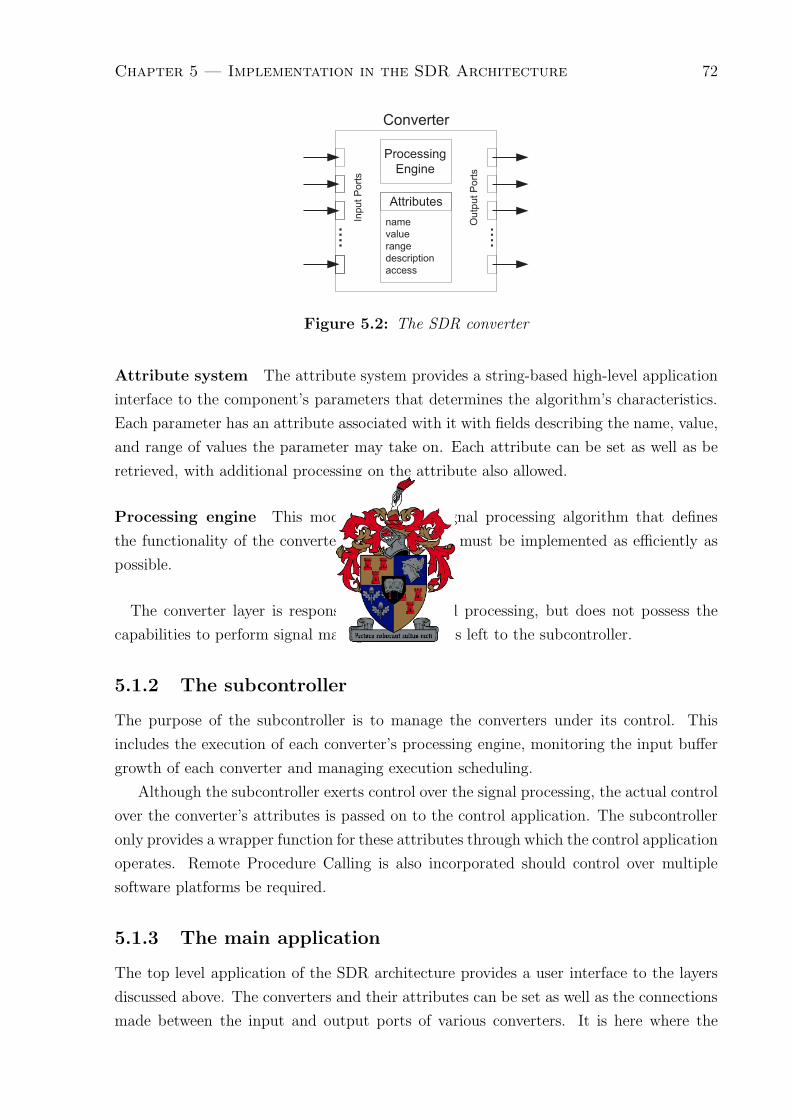
Chapter 5 — Implementation in the SDR Architecture 72
Converter
Attributes
name
value
range
description
access
Input
Port
s
Ou
tputP
ort
s
Processing
Engine
Figure 5.2: The SDR converter
Attribute system The attribute system provides a string-based high-level application
interface to the component’s parameters that determines the algorithm’s characteristics.
Each parameter has an attribute associated with it with fields describing the name, value,
and range of values the parameter may take on. Each attribute can be set as well as be
retrieved, with additional processing on the attribute also allowed.
Processing engine This module holds the signal processing algorithm that defines
the functionality of the converter. The algorithm must be implemented as efficiently as
possible.
The converter layer is responsible for all signal processing, but does not possess the
capabilities to perform signal management. This is left to the subcontroller.
5.1.2 The subcontroller
The purpose of the subcontroller is to manage the converters under its control. This
includes the execution of each converter’s processing engine, monitoring the input buffer
growth of each converter and managing execution scheduling.
Although the subcontroller exerts control over the signal processing, the actual control
over the converter’s attributes is passed on to the control application. The subcontroller
only provides a wrapper function for these attributes through which the control application
operates. Remote Procedure Calling is also incorporated should control over multiple
software platforms be required.
5.1.3 The main application
The top level application of the SDR architecture provides a user interface to the layers
discussed above. The converters and their attributes can be set as well as the connections
made between the input and output ports of various converters. It is here where the

Chapter 5 — Implementation in the SDR Architecture 73
softmodem will be built up from the individual modem components described in the
previous chapters. Further control by this layer is not allowed.
5.2 Modem implementation
The software modem was implemented in the SDR architecture just discussed. Now the
components’ and the modem controller’s implementations will be addressed, which is
followed by a description of the full modem.
5.2.1 Overview of software components
The functional blocks discussed in detail in Chapters 3 and 4 are built into the converter
layer as components. At the end of a section on each component in these chapters, a
table was given for the specific component’s interface parameters. These consisted of
descriptions of the ports and attributes for the component, which are now incorporated
into the architecture. Figure 5.4 on p. 77 shows the different components of the modem as
well as their interconnections. The naming convention in the architecture is also shown by
the names of the components, with each component grouped under a category (modem,
codec, protocol et cetera). The interface between the physical and data link layer is
controlled by the V.32 bis modem controller and it is discussed in the next section.
5.2.2 Modem Controller
The modem controller has to have the ability to control the signal flow to the data link
layer, since not all signals received are meant for the next layer. These signals form part
of the initiate and training sequence and terminates at the controller. It is therefore
important for the controller to also have the ability to change the attributes of the other
components as to condition the modem for other signals.
A feature of the architecture is that converters cannot change the attributes of another
converter. Attributes can only be changed by the main application, which means that
the developer of a system determines the value of each component’s attributes before
the subcontroller is executed. For a simple application this is adequate, but for a more
complex system, where attributes may change at runtime, this would not suffice.
A new type of component, although based on the structure of a converter, was defined
that could change another converter’s attribute. This component was used as base for
the modem controller, which had to be able to change parameters of other converters,
especially for synchronisation purposes. On the converter level, access to a converter’s
attributes should not be possible, since the only function of a converter is to perform some

Chapter 5 — Implementation in the SDR Architecture 74
10 32 54 76
Dormant
Channel
128T 1280T16T 16T16T
Data
128T
S S TRN R E B1
8
Figure 5.3: Initialisation and training sequences defined in V.32 bis
kind of signal processing on its input. Thus to keep this distinction, a tag had to be used
to differentiate between a normal converter and the new component.
An alternative way of implementing a modem controller would be to enhance the con-
verter layer by giving it the ability to incorporate one converter into another. This would
expand the converter layer to a multiple layered structure, transferring the responsibility
of attribute changes to a top converter layer. Currently this top layer is the subcontroller
layer. This option was not considered because of the implications it would have on the
rest of the architecture.
5.2.3 Modem controller at transfer initiation
The initialisation and training sequences of the software modem are based on that of the
V.32 bis standard. During runtime, the attributes of the components have to change as to
comply to the conditions presented in the standard. In addition to providing a description
of the sequences, the control the modem controller exerts on the underlying components
are also illustrated.
The different stages of the initialisation and training sequences are illustrated in Figure
5.3. During each stage the attributes of one or more components are changed to suite
that stage of the sequence. The beginning of each stage is numbered and the name of the
stage is indicated inside the blocks. The period of each stage is shown in multiples of the
symbol period. A description of what occurs at each indicated instance follows:
0. During initialisation minimal attributes are set. Since most of the components do
not feature during the initial stages of data transfer, the attributes of the components
are by default set to make the components appear transparent. Although the input
is duplicated on the output, the components still, however, remain active with signal
processing to achieve the transparency. The attributes of some components are also
set for fast acquisition during synchronisation.
1. The AGC monitors the incoming samples from the sound card. When a signal pres-
ence is detected for a predetermined period, the samples are no longer disregarded
by the AGC and are passed through to the next component. The S sequence is a

Chapter 5 — Implementation in the SDR Architecture 75
Table 5.1: Attributes changed by modem controller for stage 3
Stage Component Attribute Value
3 agc stepsize 0.001
symbsync bandwidth 0.001
carrsync bandwidth 0.001
lms stepsize 0.01
BPSK signal that alternates between the two symbols which is used by the symbol
and carrier synchronisers to attain lock.
2. The S sequence starts when two identical symbols are received, followed still with
the alternation between the two symbols. The instance is used as a reference to
time the rest of the sequences that are to follow. The orientation of the quadrature
carriers is also determined. No changes are made to attributes.
3. The training sequence, denoted TRN, is generated by incorporating the scrambler
and supplying it with binary ones. The random bitstream enters the bit to integer
converter, which is set to output dibits (two bits) and where the most significant bit
of the dibit serve as an index for the BPSK constellation. The adaptive equaliser is
set to train.
4. After 256 symbols into the training sequence, the constellation changes from a BPSK
to a QPSK signal space. Here a new constellation is loaded which uses the whole
dibit.
5. The training sequence ends after 1280 symbols. The differential encoder becomes
operational and the rate signal, R, is transmitted.
6. Following the rate signal is the terminating rate signal (E). This is used to identify
the data rate at which the data transfer will continue.
7. Up to this point QPSK was used. The data rate provided by the above stage is now
used to determine which attributes must be set for the required rate. The transfer
begins with binary ones supplied to the scrambler until 128 symbol periods was
generated at the new rate. This is denoted by B1. The equaliser continues with
further training.
8. The actual data transfer begins at the rate provided in the rate signal.
For illustration purposes, the attributes that the modem controller change in the
receiver at runtime is given in Table 5.1 for stage 3. The time response of the first three

Chapter 5 — Implementation in the SDR Architecture 76
components is made slower since these components have completed their acquisition stages
prior to this one. The equaliser starts its training by changing the stepsize from zero to
0.01.
Up to when the actual data transfers begin, a second identical bit stream is reproduced
which is used to train the equaliser. This stream also allows it to be compared with the
incoming signal to determine whether a sudden disruption of any sort occurred in the
channel. If detected, the modem could resort to stage 0.
5.2.4 The modem in the SDR architecture
Figure 5.4 shows the modem with all of its components. To interface with a DAC or an
ADC, the particular data acquisition component is linked as shown at the bottom of the
figure. The top component represents the interface to the data link layer, which, for the
modem’s evaluation, was the ymodem file transfer protocol.
The port numbers used in the connections are shown for all the components. For
various components in the receiver, Port 1 is skipped and not connected. This port is
reserved for future use as fractionally spaced processing was not considered in this project.
The extra port would then be used in conjuntion with Port 0 and consequently represent
the fraction of the current sample’s position relative to the symbol instance as determined
by the symbol timing recovery algorithm.
Another observation to be made is that the receiver and transmitter work in parallel,
in other words, they perform their tasks at the same time as required by the V.32 bis
standard.
5.3 Concepts implemented for improved robustness
and functionality
5.3.1 Modifications to the architecture
With the advent of this project, key elements was identified that the architecture lacked
or needed improvement on. Some issues were addressed but some was left for future
considerations. These issues were typically too large to explore and beyond the scope of
this project. The following additions and improvements were made to the architecture to
support the implementations for a software modem:
Complex baseband processing
It was decided to convert all signals to baseband, where the sample rate could be kept
to a minimum. This would decrease processing time and because it was not limited to

Chapter 5 — Implementation in the SDR Architecture 77
sdr_protocol_v32bis
sdr_codec_int2bit
sdr_codec_scramble
sdr_codec_bit2int
sdr_codec_diffenc
sdr_codec_convenc
0
1
1
1
0
0
0
0
0
0
0
0
0
0
0
0
sdr_basic_lookup
sdr_dsp_interp
sdr_modem_quadmod
sdr_basic_amp
ANALOG FRONT END
0
0
0
0
0
0
sdr_codec_int2bit
sdr_codec_descramb
sdr_codec_bit2int
sdr_codec_diffdec
0
0
0
0
0
0
0
0
00
0
0
0
0
0
0
0
sdr_basic_agc
0
0
0
0
sdr_modem_quaddem
sdr_dsp_filter
sdr_modem_symbsync
sdr_modem_carrsync
sdr_dsp_lms
sdr_codec_viterbi
0
0
0
0
0
0
1
1
2
2 3
0
1 2 3
2
3
2
0
0
sdr_basic_amp
3
ACCESS TO DATALINK LAYER
Figure 5.4: The modem as implemented in the SDR architecture.

Chapter 5 — Implementation in the SDR Architecture 78
Subcontroller
ConverterConverter*
(controller)
Control Data Flow
Signal Data Flow
Control Data Flow between Converters
Figure 5.5: Signal flow of the modified subcontroller
a frequency range, could be used for numerous applications. This required a complex
data type since all information in a passband can be represented by a complex baseband
signal. Complex variables were not supported by the architecture, so HP’s complex data
type [31] was introduced. The architecture in its conceptional phase was designed to
do casting when the buffers of different components had different data types. For the
complex variable, the imaginary part of the complex variable was dropped when casting
was performed, say complex to float. This is conceptionally wrong, because valid data
are thrown away and no mechanism exists to track this.
Although complex variables are supported in this project, it is still not transparent
in the architecture. In all the components real operations are performed on the complex
variables. This simplifies implementation as the processing is done on both channels with-
out interference from each other. The implemented components of this project support
this feature, but ideally, this should work for all existing components.
Real-time attribute retrieval
The attributes system of the architecture was originally designed to only take on values
and never change until new values were loaded. The problem with this design is that
should the value change at run-time, there is no way of retrieving the changed value. The
attribute retrieve method was altered to read the real variable first before exporting it.
Changing attributes from another converter
During the initialisation, converters are created within the subcontroller. Each of the
converters is assigned an integer, starting at zero, which is used by the subcontroller to
call each converter’s process when the subcontroller is running. The integer, or ID, is

Chapter 5 — Implementation in the SDR Architecture 79
returned to the main application if the converter was created successfully, which means
the main application can keep track of individual components.
This aspect of the architecture was used to tag the modem controller. The tag was
then used to identify the controller and read a collection of attributes from the control
attribute of the controller. The subcontroller subsequently changed the attributes of the
other components. This is illustrated in Figure 5.5.
Conclusion
All these modifications made the software modem feasible in the software defined radio
architecture. These are just implemented to achieve a functional working modem and was
not investigated for thorough system wide inclusion. This topic is left for further study.

Chapter 6
Measurements and results
The design of the modem can only be concluded with a measure of how well it operates in
all its facets. In this section the modem’s algorithms are evaluated and the performance
presented. The setup used is first illustrated followed by an evaluation on component
level. The last part of the chapter looks at the overall performance of the modem.
6.1 Evaluation setup overview
Figure 6.1 shows the setup used to evaluate the softmodem. The setup consists of the
transmitter and receiver part communicating through a simulated channel, which incor-
porates noise. The receiver and transmitter worked in parallel since the softmodem had
to be able to transmit and receive simultaneously as specified in the V.32 bis standard.
In every test the transmitter initiates the data transfer by going through the various
initiate and training sequences. These signals are than passed on to the simulated channel
where noise was added to produce a SNR = 25dB. The output of the channel is then passed
on to the receiver portion of the modem for further processing. The V.32 bis controller
processed the raw data simultaneously to and from the termination component, which
in this case was the ymodem file transfer protocol [6]. The ymodem was chosen for its
simplicity and it had streaming capabilities. The ymodem component is, however, just a
Channel
Transmitter
components
Receiver
components
V.32 bis
Controller
YMODEM
server
YMODEM
client
Figure 6.1: The setup with which the modem was evaluated
80

Chapter 6 — Measurements and results 81
0 0.1 0.2 0.3 0.4 0.5 0.6 0.7 0.8 0.9 1−55
−50
−45
−40
−35
−30
Normalized Frequency (×π rad/sample)
Mag
nitu
de (
dB)
Figure 6.2: The frequency response of the channel used in the simulation. The
sampling rate is 8000Hz
functional implementation of the standard as it was only used for evaluation on component
level and for testing packet loss rate in streaming mode during the overall performance
test of the modem.
The constellation used for the evaluation is the 16-QAM constellation defined in the
V.32 bis. It incorporates all the signal processing discussed in previous chapters and
should produce results that are easier to interpret than more complex constellations.
The channel in this setup comprises of three components: a digital filter, a delay buffer
and a noise adder. The digital filter was used to simulate a channel’s impulse response.
The channel of the telephone connection was adopted from [8] and presented a typical
landline connection. The frequency response of the channel is given in Figure 6.2. The
other two parts of the channel are self explanatory. The delay buffer is used to delay the
input by 1000 samples. The noise adder simply adds white Gaussian noise.
The route of evaluating the software modem with a simulated channel was persued
because full control over channel parameters could be achieved. The known channel
frequency response could be inserted and the amount of noise added was controlled.
However, this approach could only be taken if the simulated symbol rate was executed
faster than required in an actual system. This proved to be the case.
6.2 Evaluation on component level
6.2.1 Purpose of the experiment
The objective of the following section is to illustrate the performance of individual compo-
nents as to attain its performance on a signal that was processed by preceding components.
The specific component evaluated is shown through each of the initialisation stages of the
V.32 bis standard. Each stage has unique characteristics which will have a different effect
on each component.

Chapter 6 — Measurements and results 82
The components under discussion are all from the receiver of the softmodem. Evalua-
tion of the transmitter components is not applicable since the working of each component
was validated after their implementation. The performance of a correctly working trans-
mitter component would be constant for a predetermined set of attributes. It is only the
success of the algorithms in the receiver that could determine the quality of a link.
6.2.2 Experimental setup
For each of the selected components, the signals under investigation was duplicated at an
additional port of the component. These signals were then captured and presented here.
6.2.3 Results
The values of the specific signals tested are presented in the following paragraphs. The
components are listed starting at the AGC followed by the rest in the order a sample
would be processed. It should also be mentioned that for the AGC the number of samples
displayed are far more than the rest. This is due to the fact that the AGC operates at a
sampling rate of 8000Hz while the rest operates at the symbol frequency, which is 2400Hz.
Automatic gain control
Before reception, the transmitted signal is attenuated by the channel. It is the task of
the AGC component to adapt the input signal of the receiver to such a level that it is
suitable for further processing by the subsequent components. The reference level is set
beforehand and should correspond to that required in the subsequent components. The
reference level in this case is set to one, because the symbol synchroniser operates at a
constant energy level of one.
Figure 6.3 shows the stages the gain of the AGC goes through as well as the effect of
the specific signal has on it. The first part of the signal finds itself in the slew mode of the
AGC. In this mode the response time of the loop is made fast as to adjust the amplitude
of the signal to a more acceptable range of levels. From about n = 600, the AGC enters
the tracking mode, where the time response is reduced significantly as to not introduce
any more distortion.
At about n = 3000 there is a sudden drop. This is the result of the change over from
a BPSK to a QPSK signal, as found in the training period of the modem. The average
energy of the transmitted BPSK signal is lower that that of a QPSK signal because of
the additional quadrature channel. This means that in order to keep a constant energy
level, the BPSK signal has to be amplified by a larger gain than the QPSK. The sudden
drop is also not a problem for the modem since the components use this sequence for
synchronisation and they are not sensitive to amplitude variations.
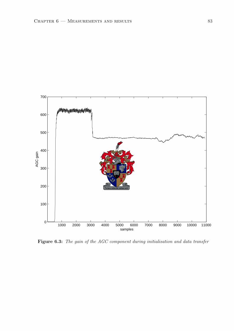
Chapter 6 — Measurements and results 83
1000 2000 3000 4000 5000 6000 7000 8000 9000 10000 110000
100
200
300
400
500
600
700
AG
C g
ain
samples
Figure 6.3: The gain of the AGC component during initialisation and data transfer
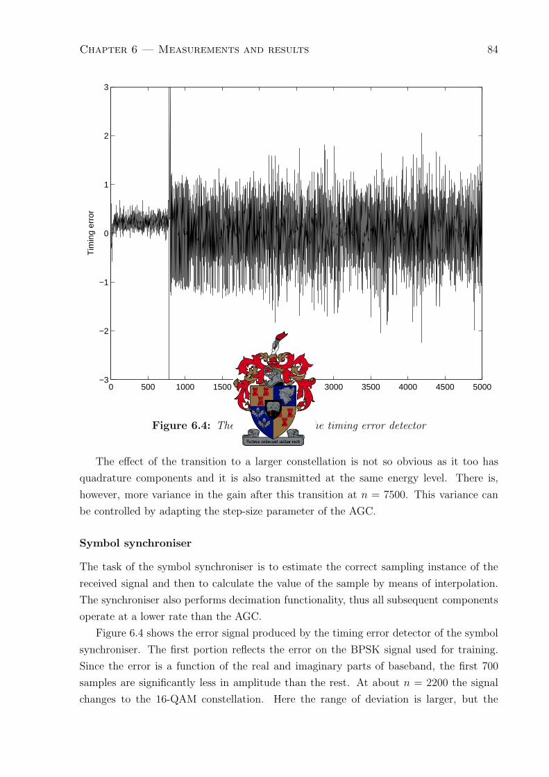
Chapter 6 — Measurements and results 84
0 500 1000 1500 2000 2500 3000 3500 4000 4500 5000−3
−2
−1
0
1
2
3T
imin
g er
ror
samples
Figure 6.4: The error signal of the timing error detector
The effect of the transition to a larger constellation is not so obvious as it too has
quadrature components and it is also transmitted at the same energy level. There is,
however, more variance in the gain after this transition at n = 7500. This variance can
be controlled by adapting the step-size parameter of the AGC.
Symbol synchroniser
The task of the symbol synchroniser is to estimate the correct sampling instance of the
received signal and then to calculate the value of the sample by means of interpolation.
The synchroniser also performs decimation functionality, thus all subsequent components
operate at a lower rate than the AGC.
Figure 6.4 shows the error signal produced by the timing error detector of the symbol
synchroniser. The first portion reflects the error on the BPSK signal used for training.
Since the error is a function of the real and imaginary parts of baseband, the first 700
samples are significantly less in amplitude than the rest. At about n = 2200 the signal
changes to the 16-QAM constellation. Here the range of deviation is larger, but the

Chapter 6 — Measurements and results 85
0 500 1000 1500 2000 2500 3000 3500 4000 4500 5000−2
−1.5
−1
−0.5
0
0.5
1
1.5P
hase
err
or in
rad
ians
samples
Figure 6.5: The phase error of the carrier synchroniser
average deviation still remains the same as the whole signal was transmitted at the same
energy.
Carrier synchroniser
The carrier synchroniser adapts a reference phasor used to rotate the received constellation
until the orientation of the quadrature axes are aligned. This is important for the Viterbi
decoder which has to deduce the correct symbol by looking at its amplitude.
The carrier synchroniser uses a phase error detector to determine the angle by which
the constellation has to be rotated. This angle is given in Figure 6.5. During initialisation
the phase error converges almost to zero, but due to noise will never reach it. This error
range is kept constant throughout transmission, showing that the synchroniser remains
locked.
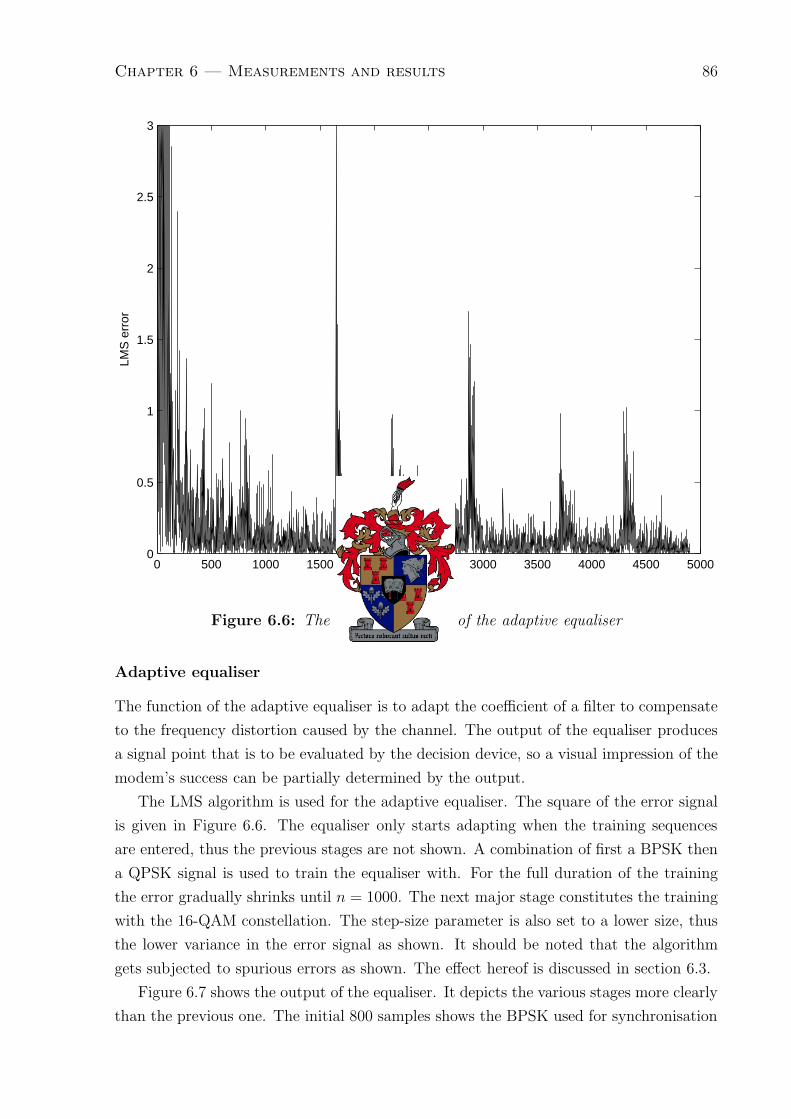
Chapter 6 — Measurements and results 86
0 500 1000 1500 2000 2500 3000 3500 4000 4500 50000
0.5
1
1.5
2
2.5
3LM
S e
rror
samples
Figure 6.6: The LMS error signal of the adaptive equaliser
Adaptive equaliser
The function of the adaptive equaliser is to adapt the coefficient of a filter to compensate
to the frequency distortion caused by the channel. The output of the equaliser produces
a signal point that is to be evaluated by the decision device, so a visual impression of the
modem’s success can be partially determined by the output.
The LMS algorithm is used for the adaptive equaliser. The square of the error signal
is given in Figure 6.6. The equaliser only starts adapting when the training sequences
are entered, thus the previous stages are not shown. A combination of first a BPSK then
a QPSK signal is used to train the equaliser with. For the full duration of the training
the error gradually shrinks until n = 1000. The next major stage constitutes the training
with the 16-QAM constellation. The step-size parameter is also set to a lower size, thus
the lower variance in the error signal as shown. It should be noted that the algorithm
gets subjected to spurious errors as shown. The effect hereof is discussed in section 6.3.
Figure 6.7 shows the output of the equaliser. It depicts the various stages more clearly
than the previous one. The initial 800 samples shows the BPSK used for synchronisation

Chapter 6 — Measurements and results 87
0 500 1000 1500 2000 2500 3000 3500 4000 4500 5000−2
−1.5
−1
−0.5
0
0.5
1
1.5
2
LMS
out
put
samples
BPSK QPSK 16−QAM
Figure 6.7: The real part of the constellation at the output of the adaptive equaliser

Chapter 6 — Measurements and results 88
without equalising. This is followed by the training with the QPSK signal. It should be
mentioned that this is only the real part of the signal and that the QPSK signal’s points
are each located at a different amplitude level, thus resembling the 16-QPSK. At n = 2000
the 16-QAM training and data transfer starts.
The component that follows the equaliser, is the Viterbi decoder. Its evaluation leads
more to a system wide evaluation and is discussed in the next section.
6.3 Overall performance of the softmodem
6.3.1 Purpose of the experiment
Now that the modem was evaluated on component level, the performance of the overall
modem is investigated. An evaluation at this level is one that will be encountered in
practice, thus key specifications must be determined.
Two things will be looked at: the error rate of the received symbols and the data
packet loss of the ymodem file transfer protocol. These two aspects will give insight into
the modem’s performance.
6.3.2 Experimental setup
The symbol error rate (SER) is the rate at which a received symbol is not assigned to the
right point in the constellation by the decision device. The test involved setting up two
lists to hold the symbol in the constellation, one for what was transmitted and one for
the output of the decision device. The list was filled by the outputs of the lookup table
and the Viterbi decoder. A symbol error rate was then extracted from this list.
The second test involved the ymodem file transfer protocol. The protocol groups the
bits into packets of 128 or 1024 bytes and with it a CRC check tag to test for errors. For
this test the packets in which the data was divided, was made 128 bytes. By looking at
how many packets are lost, the error ratio can be determined.
6.3.3 Results
The symbol error rate is given in Figure 6.8. The error rate is given along the vertical axis
while the signal to noise ratios are given on the horizontal axis. For comparison purposes,
the curve for the theoretical limit for the TCM employed in this modem is included [33],
[41].
For low signal to noise ratios, the modem couldn’t transfer data due to the high
levels of noise that interfered with the synchronisation and other components. The curve

Chapter 6 — Measurements and results 89
5 10 15 20 25 30 3510
−5
10−4
10−3
10−2
10−1
100
SNR (Es/No)
SE
R
MeasuredTheoretical
Figure 6.8: Symbol error rate for the 16-QAM modem

Chapter 6 — Measurements and results 90
5 10 15 20 25 30 35 40 45 505
10
15
20
25
30
35M
easu
red
SN
R
Input SNR
Viterbi InputTransparent System
Figure 6.9: Measured SNR vs input SNR
follows in parallel with the uncoded QAM curve until at about 17dB where it starts to
go horizontal. The symbol error rate converges to 5 × 10⁻⁵ where it remains constant.
The figure illustrates that for SNR between 10dB and 17dB the modem operates as
expected. At larger SNR this changes because the curve starts to converge to a constant
error rate, which implies that the modem is generating self noise to such a degree that
it cannot process symbols better than a rate of 5 × 10⁻⁵. This is reaffirmed in Figure
6.9 where the SNR is measured at the Viterbi decoder input. The input to the system
is given various SNR and it is then measured at the Viterbi decoder. The curve for a
transparent system (in = out) is also given.
The graph shows that for high SNR at the input, the SNR at the Viterbi decoder
input remains constant at 32dB. Between 12dB and 30dB the SNR is lower than what
is received at the input of the modem. This is because noise power is a function of
bandwidth and in the receiver the only the necessary spectrum is extracted and the rest
filtered away. Consequently, some of the noise power also gets removed. At lower SNR
the noise dominates and causes the modem not to work properly.

Chapter 6 — Measurements and results 91
Table 6.1: Expected packet loss rates for various SNR
SNR Packets lost
30dB 1/60
25dB 1/50
20dB 1/30
15dB 1/3
Table 6.2: Number of packets lost for various SNR
SNR Packets lost Packet loss rate
30dB 66 1/247
25dB 84 1/195
20dB 105 1/156
15dB 862 1/19
Ymodem test
The next test uses ymodem file transfer protocol to transfer a file from a server to a client.
With the symbol error rate known, the expected averaged packet loss of the modem can
be derived:
Total of symbols lost = Total of packets × symbols/packet × SER (6.1)
Assuming the erroneous symbols are equally spread over time and limited to one per
block, it amounts to the rates given in Table 6.1.
Table 6.2 holds the actual number of blocks lost during transmission. The packet loss
rate is given for a file transfer of 2Mb. This varies with our previous assumption with
quite a margin. After further investigation, the problem with the estimation was realised.
The errors are not evenly spread but grouped. This was traced back to the equaliser
which, as mention in its evaluation in this chapter, produces error bursts. These bursts
affect multiple symbols, thus by limiting multiple erroneous symbols to one block, reduces
the overall packet loss.
6.4 Conclusion
In this chapter the modem was evaluated to determine its performance during data trans-
fer. The test showed the key signals of significant components and their relation to the
different stages of initiation and training. Test was also done with the modem to investi-
gate the performance of the overall system regarding transmission.

Chapter 6 — Measurements and results 92
5 10 15 20 25 30 3510
−5
10−4
10−3
10−2
10−1
SNR (Es/No)
SE
R
DeducedTheoretical
Figure 6.10: Deduced symbol error rate for the 16-QAM modem
The results of the packet loss test showed that the SER graph in the first section
(Figure 6.8) is not an accurate measure for the modem. Error bursts, visible in Figure
6.7, disrupted multiple symbols in groups and it is suspected that it is due to a weak im-
plemented or wrongly setup component. In an attemp to eliminate these effects to obtain
a more accurate SER for the complete modem, the erroneous symbol groups were reduced
to one erroneous symbol, assuming that only one rogue symbol caused the disturbance.
The SER that produced the packet loss ratios was recalculated and the new deduced SER
curve is shown in 6.10. There is an overall improvement of 3-4dB over the first one, but
by eliminating the defective component a much better performance can be expected.

Chapter 7
Conclusion
This chapter provides an overview of the work done in the previous chapters of this
document. The route from initial design to complete implementation and evaluation is
repeated here. Areas of the software modem that require further research are mentioned
in the last part of this chapter.
7.1 Overview of the work
The working definition of a software defined radio was given at the beginning of Chapter 2
as: a radio that is substantially defined in software and whose physical layer behaviour
can be significantly altered through changes to its software. This idea formed the basis
for the theme of this project, which was to create a software modem by building it from
functional blocks or components.
A study into the topologies of typical software defined radios showed that all the
radios shared the same basic architecture. The mayor hardware components of a software
defined radio are:
Analog front end This portion of the radio is the only analog components of the radio.
For a perfect software radio this would include only the antenna but a more practical
implementation require additional components such as a low noise amplifier and a
mixer.
Analog to Digital Converter This converter creates a digital version of the analog
input signal. The samples are then processed digitally from here on.
Downconversion The task of the downconversion stage is to move a frequency range,
that contains the RF signal, down to IF or baseband. This range will typically be
determined by the bandwidth of the ADC.
Sample rate conversion To ease the load on the processor, a signal can be converted
93

Chapter 7 — Conclusion 94
to one with a slower sampling rate. This allows the extra processor power to be
used on other processes.
Channelisation The final component in the digital front end is channelisation. This
component performs filtering to extract the appropriate signal while attenuating
interfering neighbouring signals.
Baseband processing The final stage in the processing cycle is embedded in the decision-
driven digital signal processor. The final demodulation and decoding are performed
to retrieve the raw data stream.
The components that comprise the digital front-end are typically dedicated digital
hardware that are able to do operations in parallel and thus process samples much faster
than decision driven devices such as DSPs. However, this part becomes irrevelant when
the processing requirements are met by the decision driven processor. This was the case
to be assumed for this project provided an applicable standard can be implemented. The
V.32 bis standard was chosen for its similarities with a conventional modem.
The modem was designed from a high level perspective and then broken down into
subcomponents. These subcomponents held all the functionality of the modem thus they
could be used by other applications if they were part of a library.
The following contributions was made to the University of Stellenbosch’s SDR library.
These components were investigated from first principals in search of a generic model that
could be used by multiple applications. The main mechanism behind the algorithm of
each group of components is mentioned so as to enlighten the reader to the findings of
the investigation and possibly be the starting block for further investigations. The library
additions, divided here into algorithm groups, are:
Simple digital encoding The digital encoders of the modem, which include the differ-
ential encoder, scrambler and bit-to-integer converter, either utilised lookup tables
or used little processing power to perform their calculations. A distinct feature of
these components are that the encoder and decoder share a very similar method
of executing their task. The similarities are so close that with minor alterations
the same algorithm can be used for both functionalities. This in effect halves the
number of components in this category. Although an important observation, it was
still kept separate as to rather tag each component with a unique function for use
by other developers.
Sample rate convertion Although called and used as an interpolator, the component
evolved to one that can do both interpolation and decimation by a rational factor.
The filter attributes are completely adjustable to suit any memory and processor
limitations. Fractional interpolation not supported by the above can be achieved

Chapter 7 — Conclusion 95
by polynomial-based filters, such as used by the symbol timing recovery circuit.
Adjusting attributes of the symbol timing recovery component allows it to be a
constant fractional sample rate converter by any ratio.
Trellis coded modulation All the components associated with the trellis coding in-
corporated lookup table. Actually, all the basic mechanisms of these components
use just lookup tables, with just the metric calculation requiring the most of the
processing power. To keep it generic, these were kept to being calculated, though
using lookup tables for these is also possible. Since all of the components are basi-
cally table driven, it is possible to virtually define and implement any trellis coded
mechanism, limited, of course to the field of communications.
Down and upconversion Moving a complex signal from one frequency to another re-
quires the multiplication with a complex rotating phasor. Mixing the phasor with a
complex signal does not produce any images of the signal at other frequencies, thus
no filtering is required. This multiplication is used by the quadrature modulator and
demodulator for up and down conversion, but with the conversion to a real signal an
additional function must be incorporated as well. The carrier recovery circuit also
uses the complex phasor with multiplication, but with a lead and lag function built
in. This component can thus take over the functionality of the other mentioned
components, but, again, they were made seperate functions for other developers.
Automatic gain control The AGC’s function is to adjust the amplitude of the incom-
ing signal to a level that is acceptable for subsequent processing. To compensate
for a large dynamic range, modes were introduced where for large errors, very fast
adaptations allowed for faster acquisition of the correct energy level.
Filters Fixed (image rejection filter) and variable coefficient (adaptive equaliser) filters
use the same structure of computation to calculate its output. The difference is
that the variable coefficient filter requires additional processing power to calculate
the coefficient, which usually requires some form of feedback from outside the filter.
Thus by using a variable coefficient filter with the feedback disconnected, it changes
to a fixed coefficient filter.
The components are able to process a sample from the raw data it receives to the
modulated signal that is send via the DAC. To do anything additional such as changing
attributes for equaliser training, an independent controller is required that can control all
the components’ attributes at run-time. A concept for such a platform was provided and
illustrated with the modem. It is just a functional implementation thus further investi-
gation may be required. The same applies to the new data types that were introduced:

Chapter 7 — Conclusion 96
the complex data type and the matrix data type. These again were implemented as
prototypes and needs further looking into.
7.2 Future work
Although the modem, and more specifically its subcomponents, enabled means of com-
munication over a basic channel, the ideal would be to communicate over a variety of
channels using the same software. The platform was set to take the existing components
and improve on them to make them more suitable to the variety of channels. The same
counts for the concept of the controller, which definitely needs further investigation.
The different components created were all designed to be generic yet, at the same
time, perform their tasks very efficiently. These conflicting goals result in a trade off to be
considered between being generic and being efficient. To be efficient does not necessarily
mean that something is generic because it must then cater for all, or a certain range, of
conditions. This trade off is however in some instances limited by technology only. An
example of such a limitation is discussed by [21] where the mechanism of channelisation
and despreading can mathematically be done with the same hardware, but the speeds
required are not feasible. This ideas can be further explored by combining components
already implemented.
In [3], the Moore’s law equivalent for data transfer speeds over wired and wireless
channels was deduced from the progress made in these fields. The trends show that the
speeds achieved over both channels will eventually reach the same point. At this stage
there might not be a differentiation between the channels, or technologies, anymore as
the speeds mentioned do not match anything existing today. The result is an high speed
software radio suited for every environment. The expectation is set, and with that a goal
to persue.

Bibliography
[1] “Softmodem.” www.wikipedia.org.
[2] “Softmodem.org: A GNU kind of modem.” www.softmodem.org.
[3] “Moore’s law equivalent for data transfer speeds.” IEEE Spectrum, July 2004,
pp. 58–59.
[4] BELLARD, F. http://fabrice.bellard.free.fr/linmodem.html.
[5] CHIRAYIL, R. and LOVRICH, A., An All-Digital Automatic Gain Control . Texas
Instruments, 1997. Application Report: SPRA081.
[6] CHRISTENSEN, W., X/YMODEM Protocol Reference, 1988.
[7] CILLIERS, C. A., “Design and Implementation of a Digital Modem on the
DSP56001.” Master’s thesis, University of Stellenbosch, 1994.
[8] CLARK, A., Adaptive detectors for Digital Modems. London: Pentech Press, 1989.
[9] CRONJE, J. J., “Software Architecture Design of a Software Defined Radio
System.” Master’s thesis, University of Stellenbosch, 2004.
[10] D’ANDREA, A. N. and LUISE, M., “Optimization of Symbol Timing Recovery for
QAM Data Demodulators.” IEEE Transactions on Communications, March 1996,
Vol. 44, No. 3, pp. 399–406.
[11] DARABAN, F., “An analog voice modem with generalized Wei’s type
2N-dimensional trellis coded modulation.”
[12] ERUP, L. et al., “Interpolation in Digital Modems - Part II: Implementation and
Performance.” IEEE Transactions on Communications, June 1993, Vol. 41, No. 6,
pp. 998–1008.
[13] FARROW, C. W., “A continuously variable digital delay element.” Proc. IEEE Int.
Symp. Circuits & Systems, June 1988, Vol. 3, pp. 2641–2645.
[14] FISCHER, T. http://www-users.cs.york.ac.uk/fisher/modem/.
97

BIBLIOGRAPHY 98
[15] FRANKLIN, G. et al., Feedback Control of Dynamic Systems . Third edition.
Addison-Wesley Publishing Company, 1994.
[16] FRANKS, L., “Carrier and Bit Synchronization in Data Communication - A
Tutorial Review.” IEEE Transactions on Communications, August 1980, Vol. 28,
No. 8, pp. 1107–1121.
[17] GARDNER, F. M., “A BPSK/QPSK Timing-Error Detector for Sampled
Receivers.” IEEE Transactions on Communications, May 1986, Vol. 34, No. 5,
pp. 423–429.
[18] HARRIS, F., “Carrier Synchronization Techniques for DSP-Based Modems.”
CommsDesign.
[19] HAYKIN, S., Digital Communications . New York: John Wiley & Sons, 1988.
[20] HAYKIN, S., Adaptive Filter Theory . Third edition. New Jersey: Prentice Hall,
1996.
[21] HENTSCHEL, T. et al., “The Digital Front-End of Software Radio Terminals.”
IEEE Personal Communications, August 1999.
[22] HENTSCHEL, T. and FETTWEIS, G., “Sample Rate Conversion for Software
Radio.” IEEE Communications Magazine, August 2000, pp. 142–150.
[23] HOROWITZ, P. and HILL, W., The art of electronics . Second edition. Cambridge:
Cambridge University Press, 1996.
[24] INTERNATIONAL TELECOMMUNICATION UNION. A duplex modem
operating at data signalling rates of up to 14 400 bit/s for use on the general
switched telephone network and on leased point-to-point 2-wire telephone-type
circuits , 1994. ITU-T V.32bis.
[25] INTERNATIONAL TELECOMMUNICATION UNION. A digital modem and
analogue modem pair for use on the public switched telephone network (PSTN) at
data signalling rates of up to 56 000 bit/s downstream and up to 33 600 bit/s
upstream, 1998. ITU-T V.90.
[26] INTERNATIONAL TELECOMMUNICATION UNION. A modem operating at
data signalling rates of up to 33 600 bit/s for use on the general switched telephone
network and on leased point-to-point 2-wire telephone-type circuits, 1998. ITU-T
V.34.
[27] ITU, “International Telecommunications Union.” www.itu.int.

BIBLIOGRAPHY 99
[28] KIRKE, T., “Interpolation, Resampling and Structures for Digital Receiver.”
CommsDesign, February 2004.
[29] LITWIN, L., “Matched filtering and timing recovery in digital receivers.” RF
Design, September 2001, Vol. 20, No. 6, pp. 32–48.
[30] MASSEY, T. and IYER, R., DSP Solutions for Telephony and Data/Facsimile
Modems , 1997.
[31] MICROSYSTEMS, S., “Using the Complex Arithmetic Library.”
http://docs.sun.com/source/819-0496/Complex.html. 1997.
[32] PANAYIOTOPOULOS, I., “Unified Algebraic Treatment of Synchronization
Parameters Estimation.”
[33] PROAKIS, J. G. and MANOLAKIS, D. G., Digital Signal Processing: Principles,
Algorithms, and Applications. Third edition. New Jersey: Prentice Hall, 1996.
[34] PROAKIS, J., Digital Communication. Second edition. New York: McGraw-Hill,
1989.
[35] REED, J. H., Software Radio: A Modern Approach to Radio Engineering . New
Jersey: Prentice Hall PTR, 2002.
[36] TACCONI, E. J. and CHRISTIANSEN, C. F., “A Wide Range and High Speed
Automatic Gain Control.” IEEE PAC, 1993.
[37] TEXAS INSTRUMENTS. Implementing V.32bis Viterbi Decoding on the
TMS320C62xx DSP , April 1998.
[38] TREICHLER, J. and LARIMORE, M., “Voiceband Modems: A Signal Processing
Success Story.” IEEE Signal Processing Magazine, 1999, Vol. 16, No. 3, No. 3,
pp. 21–25.
[39] TUTTLEBEE, W. (Ed.), Baseband Processing for SDR. England: John Wiley &
Sons, 2002.
[40] UNGERBOECK, G., “Trellis-Coded Modulation with Redundant Signal Sets Part
1: Introduction.” IEEE Communications Magazine, February 1987, Vol. 25, No. 2,
pp. 5–11.
[41] UNGERBOECK, G., “Trellis-Coded Modulation with Redundant Signal Sets Part
2: State of the Art.” IEEE Communications Magazine, February 1987, Vol. 25,
No. 2, pp. 12–21.

BIBLIOGRAPHY 100
[42] VANKKA, J., “Methods of Mapping from Phase to Sine Amplitude in Direct
Digital Synthesis.” IEEE Transactions on Ultrasonics, Ferroelectrics, and
Frequency Control, March 1997, Vol. 44, No. 2, pp. 526–534.
[43] VO, N. D. and LE-NGOC, T., “Optimal Interpolators for Flexible Digital
Receivers.”
[44] WATKINS, G., “Optimal Farrow Coefficients for Symbol Timing Recovery.” IEEE
Communications Letters, September 2001, Vol. 5, No. 9, pp. 381–383.
[45] WEI, L.-F., “Rotationally Invariant Convolutional Channel Coding with Expanded
Signal Space - Part I: 180◦.” IEEE Journal on Selected Areas in Communications,
September 1984, Vol. 2, No. 5, pp. 659–671.
[46] WEI, L.-F., “Rotationally Invariant Convolutional Channel Coding with Expanded
Signal Space - Part II: Nonlinear Codes.” IEEE Journal on Selected Areas in
Communications, September 1984, Vol. 2, No. 5, pp. 672–686.
[47] WYLIE, C. R. and BARRET, L. C., Advanced Engineering Mathematics.
Sixth edition. United States of America: McGraw-Hill, 1995.