socket fm2 design specification - amd.com · advanced micro devices . socket fm2 design...
TRANSCRIPT
Advanced Micro Devices
Socket FM2 Design Specification
Publication # 48639 Revision: 3.00 Issue Date: April 2014
Specification Agreement This Specification Agreement (this “Agreement”) is a legal agreement between Advanced Micro Devices, Inc. (“AMD”) and “You” as the recipient of the attached AMD Specification (the “Specification”). If you are accessing the Specification as part of your performance of work for another party, you acknowledge that you have authority to bind such party to the terms and conditions of this Agreement. If you accessed the Specification by any means or otherwise use or provide Feedback (defined below) on the Specification, You agree to the terms and conditions set forth in this Agreement. If You do not agree to the terms and conditions set forth in this Agreement, you are not licensed to use the Specification; do not use, access or provide Feedback about the Specification.
In consideration of Your use or access of the Specification (in whole or in part), the receipt and sufficiency of which are acknowledged, You agree as follows:
1. You may review the Specification only (a) as a reference to assist You in planning and designing Your product, service or technology (“Product”) to interface with an AMD product in compliance with the requirements as set forth in the Specification and (b) to provide Feedback about the information disclosed in the Specification to AMD.
2. Except as expressly set forth in Paragraph 1, all rights in and to the Specification are retained by AMD. This Agreement does not give You any rights under any AMD patents, copyrights, trademarks or other intellectual property rights. You may not (i) duplicate any part of the Specification; (ii) remove this Agreement or any notices from the Specification, or (iii) give any part of the Specification, or assign or otherwise provide Your rights under this Agreement, to anyone else.
3. The Specification may contain preliminary information, errors, or inaccuracies, or may not include certain necessary information. Additionally, AMD reserves the right to discontinue or make changes to the Specification and its products at any time without notice. The Specification is provided entirely “AS IS.” AMD MAKES NO WARRANTY OF ANY KIND AND DISCLAIMS ALL EXPRESS, IMPLIED AND STATUTORY WARRANTIES, INCLUDING BUT NOT LIMITED TO IMPLIED WARRANTIES OF MERCHANTABILITY, FITNESS FOR A PARTICULAR PURPOSE, NONINFRINGEMENT, TITLE OR THOSE WARRANTIES ARISING AS A COURSE OF DEALING OR CUSTOM OF TRADE. AMD SHALL NOT BE LIABLE FOR DIRECT, INDIRECT, CONSEQUENTIAL, SPECIAL, INCIDENTAL, PUNITIVE OR EXEMPLARY DAMAGES OF ANY KIND (INCLUDING LOSS OF BUSINESS, LOSS OF INFORMATION OR DATA, LOST PROFITS, LOSS OF CAPITAL, LOSS OF GOODWILL) REGARDLESS OF THE FORM OF ACTION WHETHER IN CONTRACT, TORT (INCLUDING NEGLIGENCE) AND STRICT PRODUCT LIABILITY OR OTHERWISE, EVEN IF ADVISED OF THE POSSIBILITY OF SUCH DAMAGES.
4. Furthermore, AMD’s products are not designed, intended, authorized or warranted for use as components in systems intended for surgical implant into the body, or in other applications intended to support or sustain life, or in any other application in which the failure of AMD’s product could create a situation where personal injury, death, or severe property or environmental damage may occur.
5. You have no obligation to give AMD any suggestions, comments or feedback (“Feedback”) relating to the Specification. However, any Feedback You voluntarily provide may be used by AMD without restriction, fee or obligation of confidentiality. Accordingly, if You do give AMD Feedback on any version of the Specification, You agree AMD may freely use, reproduce, license, distribute, and otherwise commercialize Your Feedback in any product, as well as has the right to sublicense third parties to do the same. Further, You will not give AMD any Feedback that You may have reason to believe is (i) subject to any patent, copyright or other intellectual property claim or right of any third party; or (ii) subject to license terms which seek to require any product or intellectual property incorporating or derived from Feedback or any Product or other AMD intellectual property to be licensed to or otherwise provided to any third party.
6. You shall adhere to all applicable U.S., European, and other export laws, including but not limited to the U.S. Export Administration Regulations (“EAR”), (15 C.F.R. Sections 730 through 774), and E.U. Council Regulation (EC) No 428/2009 of 5 May 2009. Further, pursuant to Section 740.6 of the EAR, You hereby certifies that, except pursuant to a license granted by the United States Department of Commerce Bureau of Industry and Security or as otherwise permitted pursuant to a License Exception under the U.S. Export Administration Regulations ("EAR"), You will not (1) export, re-export or release to a national of a country in Country Groups D:1, E:1 or E:2 any restricted technology, software, or source code You receive hereunder, or (2) export to Country Groups D:1, E:1 or E:2 the direct product of such technology or software, if such foreign produced direct product is subject to national security controls as identified on the Commerce Control List (currently found in Supplement 1 to Part 774 of EAR). For the most current Country Group listings, or for additional information about the EAR or Your obligations under those regulations, please refer to the U.S. Bureau of Industry and Security’s website at http://www.bis.doc.gov/.
7. If You are a part of the U.S. Government, then the Specification is provided with “RESTRICTED RIGHTS” as set forth in subparagraphs (c) (1) and (2) of the Commercial Computer Software-Restricted Rights clause at FAR 52.227-14 or subparagraph (c) (1)(ii) of the Rights in Technical Data and Computer Software clause at DFARS 252.277-7013, as applicable.
8. This Agreement is governed by the laws of the State of California without regard to its choice of law principles. Any dispute involving it must be brought in a court having jurisdiction of such dispute in Santa Clara County, California, and You waive any defenses and rights allowing the dispute to be litigated elsewhere. If any part of this agreement is unenforceable, it will be considered modified to the extent necessary to make it enforceable, and the remainder shall continue in effect. The failure of AMD to enforce any rights granted hereunder or to take action against You in the event of any breach hereunder shall not be deemed a waiver by AMD as to subsequent enforcement of rights or subsequent actions in the event of future breaches. This Agreement is the entire agreement between You and AMD concerning the Specification; it may be changed only by a written document signed by both You and an authorized representative of AMD.
© 2010 – 2014 Advanced Micro Devices, Inc. All rights reserved.
The information contained herein is for informational purposes only, and is subject to change without notice. While every precaution has been taken in the preparation of this document, it may contain technical inaccuracies, omissions and typographical errors, and AMD is under no obligation to update or otherwise correct this information. Advanced Micro Devices, Inc. makes no representations or warranties with respect to the accuracy or completeness of the contents of this document, and assumes no liability of any kind, including the implied warranties of noninfringement, merchantability or fitness for particular purposes, with respect to the operation or use of AMD hardware, software or other products described herein. No license, including implied or arising by estoppel, to any intellectual property rights is granted by this document. Terms and limitations applicable to the purchase or use of AMD’s products are as set forth in a signed agreement between the parties or in AMD's Standard Terms and Conditions of Sale. Trademarks
AMD, the AMD Arrow logo, and combinations thereof are trademarks of Advanced Micro Devices, Inc. Other product names used in this publication are for identification purposes only and may be trademarks of their respective companies.
Dolby Laboratories, Inc. Manufactured under license from Dolby Laboratories.
Rovi Corporation This device is protected by U.S. patents and other intellectual property rights. The use of Rovi Corporation's copy protection technology in the device must be authorized by Rovi Corporation and is intended for home and other limited pay-per-view uses only, unless otherwise authorized in writing by Rovi Corporation. Reverse engineering or disassembly is prohibited. USE OF THIS PRODUCT IN ANY MANNER THAT COMPLIES WITH THE MPEG ACTUAL OR DE FACTO VIDEO AND/OR AUDIO STANDARDS IS EXPRESSLY PROHIBITED WITHOUT ALL NECESSARY LICENSES UNDER APPLICABLE PATENTS. SUCH LICENSES MAY BE ACQUIRED FROM VARIOUS THIRD PARTIES INCLUDING, BUT NOT LIMITED TO, IN THE MPEG PATENT PORTFOLIO, WHICH LICENSE IS AVAILABLE FROM MPEG LA, L.L.C., 6312 S. FIDDLERS GREEN CIRCLE, SUITE 400E, GREENWOOD VILLAGE, COLORADO 80111.
48639 Rev. 3.00 April 2014 Socket FM2 Design Specification
Contents 5
Contents Revision History ............................................................................................................................... 9
Chapter 1 Introduction ............................................................................................................ 10
1.1 5B5B5B5BPurpose ............................................................................................................................. 10
1.2 6B6B6B6BSupplier Requirements ..................................................................................................... 11
Chapter 2 Microprocessor Package Description ................................................................... 12
Chapter 3 Socket Mechanical Requirements ........................................................................ 13
3.1 7B7B7B7BSocket Outline .................................................................................................................. 13
3.2 8B8B8B8BPackage Seating Plane ..................................................................................................... 15
3.2.1 34B34B34B33BPackage Supports and Seating Plane Dimensional Requirements ........................... 16
3.2.2 35B35B35B34BMeasurement Method for Package Supports and Seating Plane ............................. 16
3.3 9B9B9B9BSocket Base and Socket Cover ........................................................................................ 21
3.3.1 Socket Cover Hole ................................................................................................... 21
3.3.2 Socket Cover Finger Access .................................................................................... 21
3.3.3 36B36B36B36BSocket Markings ...................................................................................................... 21
3.4 10B10B10B10BSocket Contact ................................................................................................................. 22
3.4.1 37B37B37B37BContact Base Metal .................................................................................................. 22
3.4.2 38B38B38B38BContact Plating ......................................................................................................... 22
3.4.3 39B39B39B39BSurface Mount Technology (SMT) Solder Balls ..................................................... 22
3.5 11B11B11B11BSocket Actuation Lever ................................................................................................... 22
3.5.1 40B40B40B40BLever Material .......................................................................................................... 23
3.5.2 41B 41B41B41BPackage Insertion and Extraction Force .................................................................. 23
3.5.3 42B42B42B42BSocket Retention Force ............................................................................................ 23
3.5.4 43B43B43B43BLocking Latch .......................................................................................................... 23
3.5.5 44B44B44B44BLever Actuation and Deactuation Force .................................................................. 23
3.5.6 45B45B45B45BPin Field Actuation Displacement ........................................................................... 23
3.6 12B12B12B12BSocket Durability ............................................................................................................. 23
3.7 13B13B13B13BVisual Inspection ............................................................................................................. 23
3.7.1 46B46B46B46B Solder Balls ............................................................................................................. 23
3.7.2 47B47B47B47BContacts.................................................................................................................... 24
3.7.3 48B48B48B48BCover and Base ........................................................................................................ 24
Socket FM2 Design Specification 48639 Rev. 3.00 April 2014
6 Contents
3.7.4 49B49B49B49BActuation Lever ....................................................................................................... 24
3.8 14B14B14BCritical-to-Function Parameter List ................................................................................ 24
Chapter 4 Socket Electrical Requirements ........................................................................... 26
4.1 15B15B15B14BContact Current Rating.................................................................................................... 26
4.2 16B16B16B15BLow Level Circuit Resistance (LLCR) ........................................................................... 26
4.2.1 50B50B50B50BInitial Resistance ..................................................................................................... 26
4.2.2 51B51B51B51BFinal Resistance ....................................................................................................... 26
4.3 17B17B17B16BInductance ....................................................................................................................... 26
4.4 18B18B18B17BCapacitance ..................................................................................................................... 27
4.5 19B19B19B18BDifferential Impedance .................................................................................................... 27
4.6 20B20B20B19BPropagation Delay ........................................................................................................... 27
4.7 21B21B21B20BCross Talk ....................................................................................................................... 27
4.8 22B22B22B21BDielectric Withstanding Voltage (DWV) ........................................................................ 27
4.9 23B23B23B22BInsulation Resistance (IR) ............................................................................................... 27
Chapter 5 Socket Environmental Requirements .................................................................. 28
5.1 24B24B24B23BThermal Shock ................................................................................................................ 28
5.2 25B25B25B24BCyclic Humidity .............................................................................................................. 28
5.3 26B26B26B25BThermal Cycling .............................................................................................................. 28
5.4 27B27B27B26BTemperature Life ............................................................................................................. 28
5.5 28B28B28B27BIndustrial Mixed Flowing Gas ........................................................................................ 29
5.6 29B29B29B28BMechanical Shock ........................................................................................................... 29
5.7 30B30B30B29BRandom Vibration ........................................................................................................... 29
5.8 31B31B31B30BResistance to Solder Heat ................................................................................................ 29
5.9 32B32B32B31BResistance to Solvents ..................................................................................................... 29
5.10 33B33B33B32BHeatsink Assembly .......................................................................................................... 29
48639 Rev. 3.00 April 2014 Socket FM2 Design Specification
List of Figures 7
List of Figures Figure 1. A 3-D View of Socket FM2 ............................................................................................. 10
Figure 2. AMD 904-Pin Organic μPGA Package Drawing (dwg # 038.843, Rev B) ..................... 12
Figure 3. Socket FM2 Outline ......................................................................................................... 14
Figure 4. Allowable PCB Component Keep-In, Keep-Out Area..................................................... 15
Figure 5. Illustration of Outer Region Measurement Points ............................................................ 17
Figure 6. Definition of Step Height ................................................................................................. 17
Figure 7. Illustration of Best Fit Plane ............................................................................................. 18
Figure 8. Illustration of the Inner Support Posts Measurement Points ............................................ 19
Figure 9. Illustration of the Center Support Ring Measurement Locations ..................................... 20
Figure 10. Illustration of Center Support Ring and Inner Support Posts Measurement Method..... 20
Socket FM2 Design Specification 48639 Rev. 3.00 April 2014
8 List of Tables
List of Tables Table 1. Package Supports and Seating Plane Dimensional Requirements .................................... 16
Table 2. Socket FM2 Critical-to-Function Parameters ................................................................... 24
48639 Rev. 3.00 April 2014 Socket FM2 Design Specification
Revision History 9
Revision History
Date Revision Description April 2014 3.00 Initial Public Release
Socket FM2 Design Specification 48639 Rev. 3.00 April 2014
10 Introduction Chapter 1
Chapter 1 Introduction
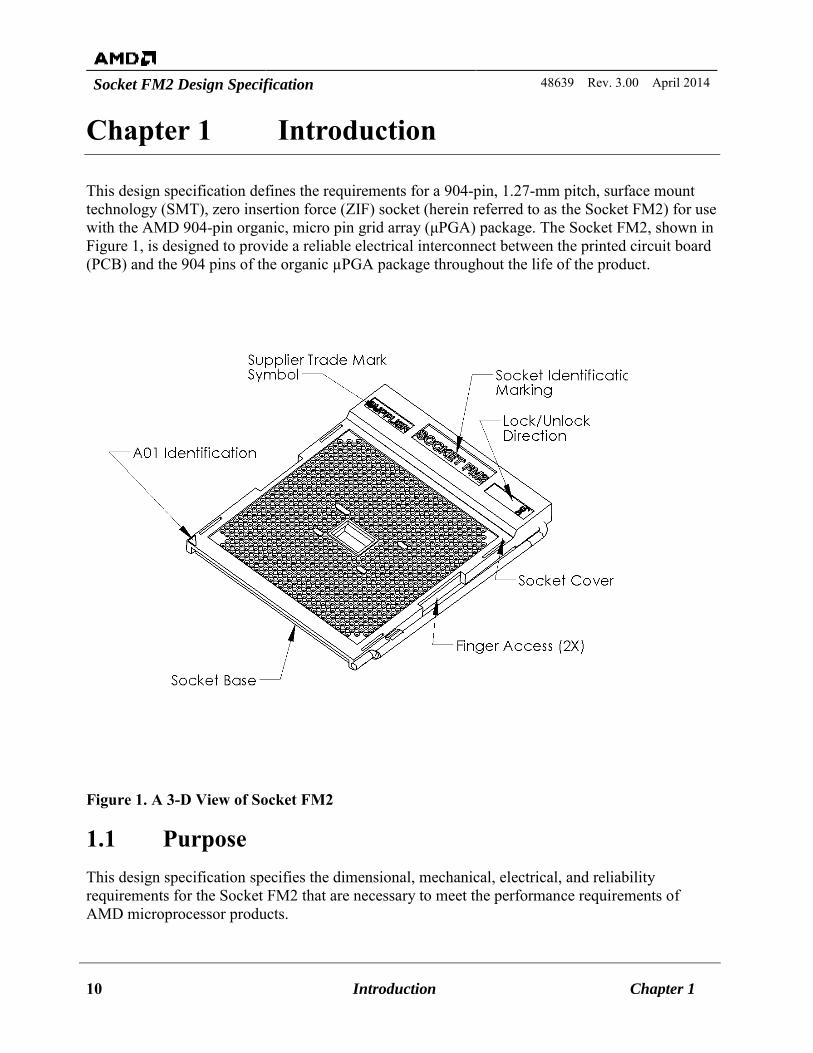
This design specification defines the requirements for a 904-pin, 1.27-mm pitch, surface mount technology (SMT), zero insertion force (ZIF) socket (herein referred to as the Socket FM2) for use with the AMD 904-pin organic, micro pin grid array (μPGA) package. The Socket FM2, shown in Figure 1, is designed to provide a reliable electrical interconnect between the printed circuit board (PCB) and the 904 pins of the organic µPGA package throughout the life of the product.
Figure 1. A 3-D View of Socket FM2
1.1 Purpose This design specification specifies the dimensional, mechanical, electrical, and reliability requirements for the Socket FM2 that are necessary to meet the performance requirements of AMD microprocessor products.
48639 Rev. 3.00 April 2014 Socket FM2 Design Specification
Chapter 1 Introduction 11
1.2 Supplier Requirements To become a qualified supplier for the Socket FM2, the potential socket supplier must demonstrate that their product meets the requirements listed in this document and must conduct qualification testing on their production run sockets in accordance with the Socket FM2 Qualification Plan, order# 48640.
Socket FM2 Design Specification 48639 Rev. 3.00 April 2014
12 Microprocessor Package Description Chapter 2
Chapter 2 Microprocessor Package Description
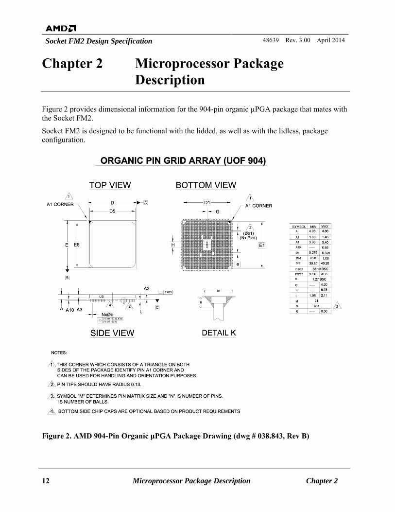
XXXXFigure 2XXXXXX provides dimensional information for the 904-pin organic µPGA package that mates with the Socket FM2.
Socket FM2 is designed to be functional with the lidded, as well as with the lidless, package configuration.
Figure 2. AMD 904-Pin Organic μPGA Package Drawing (dwg # 038.843, Rev B)
48639 Rev. 3.00 April 2014 Socket FM2 Design Specification
Chapter 3 Socket Mechanical Requirements 13
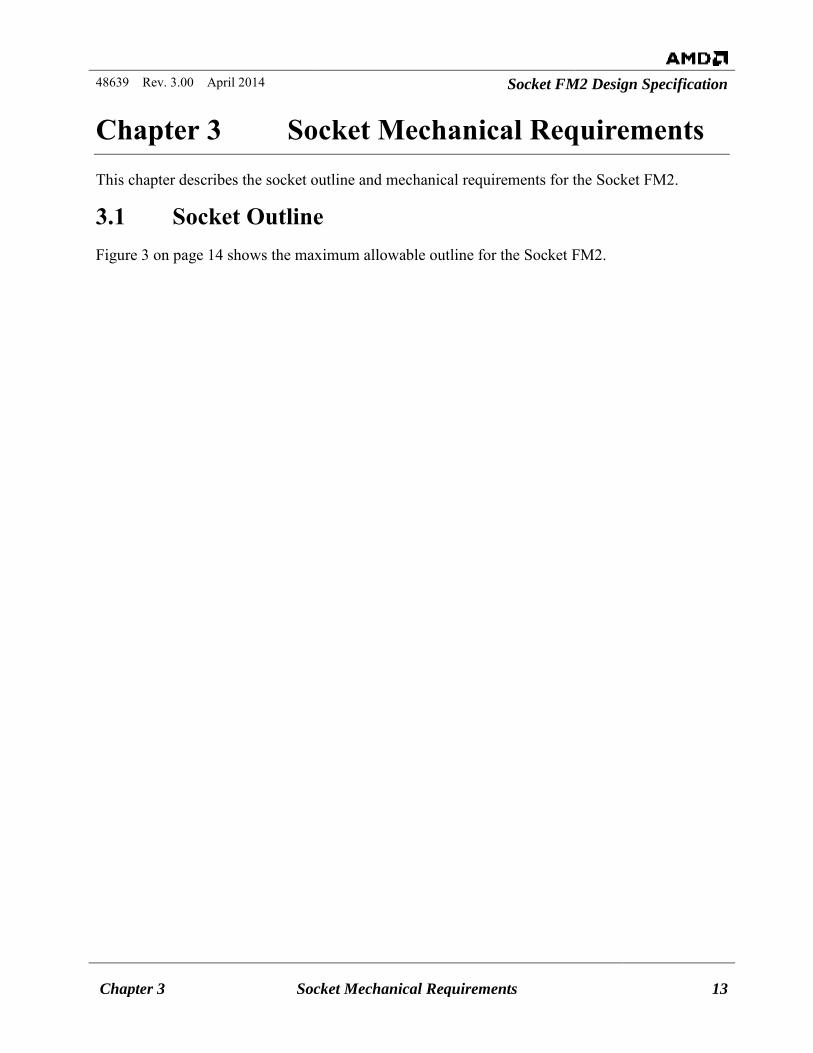
Chapter 3 Socket Mechanical Requirements This chapter describes the socket outline and mechanical requirements for the Socket FM2.
3.1 Socket Outline X XXXFigure 3 on page 14XXXX shows the maximum allowable outline for the Socket FM2.
Socket FM2 Design Specification 48639 Rev. 3.00 April 2014
14 Socket Mechanical Requirements Chapter 3
Figure 3. Socket FM2 Outline
48639 Rev. 3.00 April 2014 Socket FM2 Design Specification
Chapter 3 Socket Mechanical Requirements 15
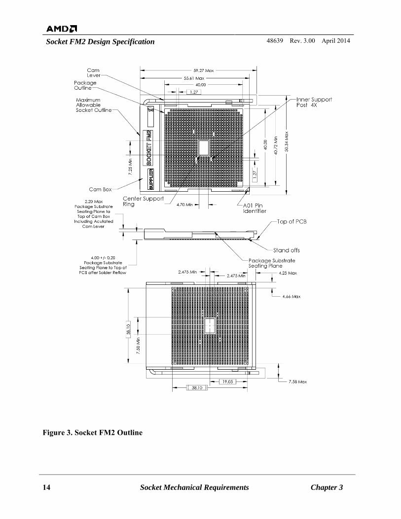
The allowable component keep-in area within the socket housing cavity on the PCB is shown in the XXXXFigure 4XXXXX. The height of the devices mounted on the PCB within the keep-in area of the socket housing must be less than 2.00 mm.
Figure 4. Allowable PCB Component Keep-In, Keep-Out Area
3.2 Package Seating Plane The cover for the Socket FM2 is designed to accommodate the package pin shoulder and braze/solder fillet as shown by the 904-pin organic µPGA package drawings in XXXXFigure 2 XXXX on page XXX12XXX. Package support structures are incorporated into the socket cover to provide sufficient mechanical support (seating plane) for the package substrate without causing damage to the package pins at any time.
Before and after SMT, the package-seating plane on the socket cover has a surface flatness of less than 0.25 mm when unmated, as well as when mated, with a package. After the socket is mounted
Socket FM2 Design Specification 48639 Rev. 3.00 April 2014
16 Socket Mechanical Requirements Chapter 3
to the PCB, the package-seating plane on the socket cover is 4.00 mm ± 0.20 mm from the mounting surface of the PCB.
3.2.1 Package Supports and Seating Plane Dimensional Requirements
To ensure proper support of the processor package while it is situated in the socket, the outer support region of the package seating plane, the center support ring, the inner support posts (indicated in XXXXFigure 3XXXX on page XXXX14XXXXXX14XXXX), and the socket base must meet the following dimensional requirements:
Table 1. Package Supports and Seating Plane Dimensional Requirements Item No.
After SMT Requirement
1 The outer support region step height is 0.30 mm ± 0.05 mm. 2 The flatness of the outer support region must not exceed 0.25 mm. 3 The inner support posts are +0.06 mm± 0.05 mm above the least mean
squares defined plane (LMS1) of the outer support region. 4 The center support ring is – 0.03 mm ± 0.05 mm from the least mean
squares defined plane (LMS2) of the inner support posts.
Refer to measurement requirements in Section XXXX3.2.2XXXX.
3.2.2 Measurement Method for Package Supports and Seating Plane
The features in Section X XXX3.2.1 X XXX must be measured using the methodologies shown in Sections XXXX3.2.2.1 XXXX through XXXX3.2.2.4 XXXX, on pages XXXX16XXXX through XXXX18 XXXX, respectively.
3.2.2.1 Measurement Conditions
The socket to be measured must be reflowed to a PCB using the recommended reflow process for the socket for the particular solder ball composition.
Note: An AMD approved fixture that maintains the socket cover in contact with the socket base at
the inner seating plane supports must be used for the socket measurement.
3.2.2.2 Outer Support Region Step Height Measurement
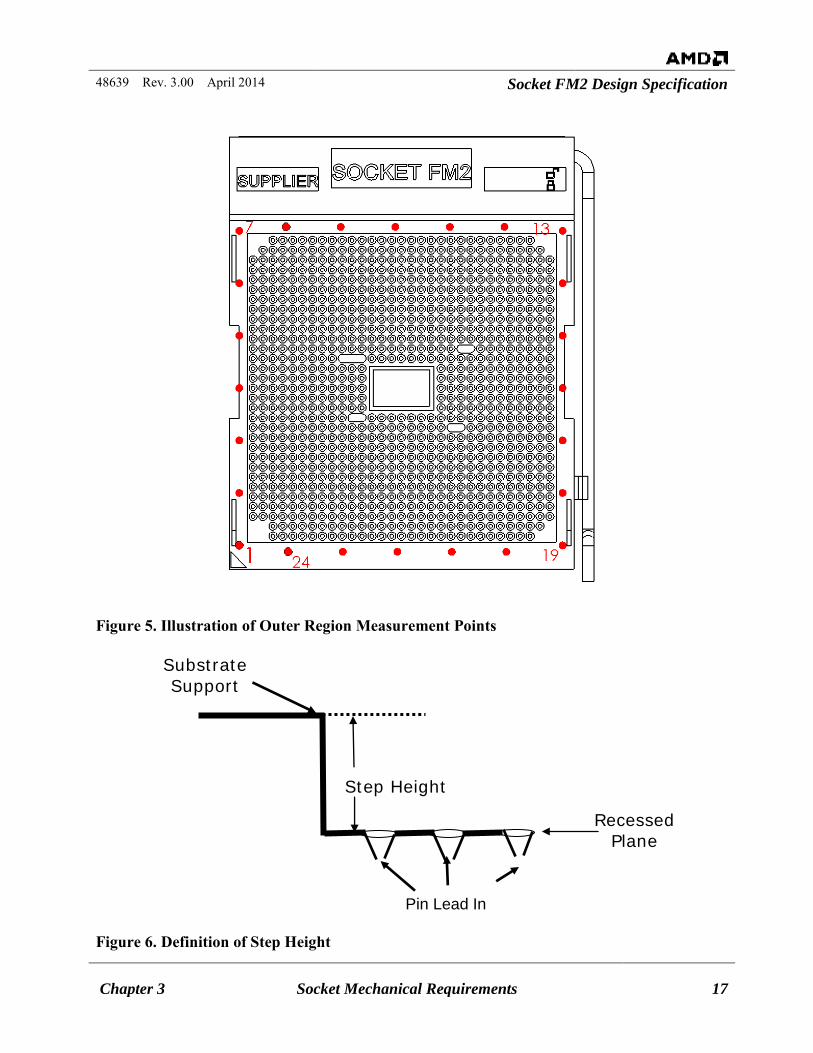
Measure the outer step height at 24 evenly-spaced points (6 per side) around the outer support using a local point-to-point method as shown in XXXXFigure 5 on page 17XXXX.
The step height is the difference in height between a point on the outer support region and an adjacent point on the recessed plane of the socket. See XXXXFigure 6XXXX, on page XXXX17XXXX, for the definition of step height.
Note: The step height must conform to the dimensional requirements of item 1, in XXXXTable 1XXXX on
page X XXX16XXXXXX16XXX.
48639 Rev. 3.00 April 2014 Socket FM2 Design Specification
Chapter 3 Socket Mechanical Requirements 17
Figure 5. Illustration of Outer Region Measurement Points
Figure 6. Definition of Step Height
Recessed Plane
Substrate
Support
Step Height
Pin Lead In
Socket FM2 Design Specification 48639 Rev. 3.00 April 2014
18 Socket Mechanical Requirements Chapter 3
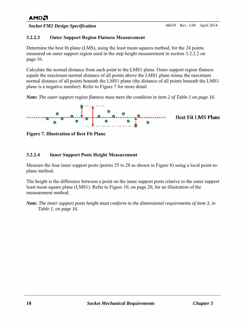
3.2.2.3 Outer Support Region Flatness Measurement
Determine the best fit plane (LMS), using the least mean squares method, for the 24 points measured on outer support region used in the step height measurement in section XXXX3.2.2.2XXXX on page XXXX16XXXX.
Calculate the normal distance from each point to the LMS1 plane. Outer support region flatness equals the maximum normal distance of all points above the LMS1 plane minus the maximum normal distance of all points beneath the LMS1 plane (the distance of all points beneath the LMS1 plane is a negative number). Refer to X XXXFigure 7XXXX for more detail.
Note: The outer support region flatness must meet the condition in item 2 of XXXXTable 1XXXX on page XXXX16 XXXX.
Figure 7. Illustration of Best Fit Plane
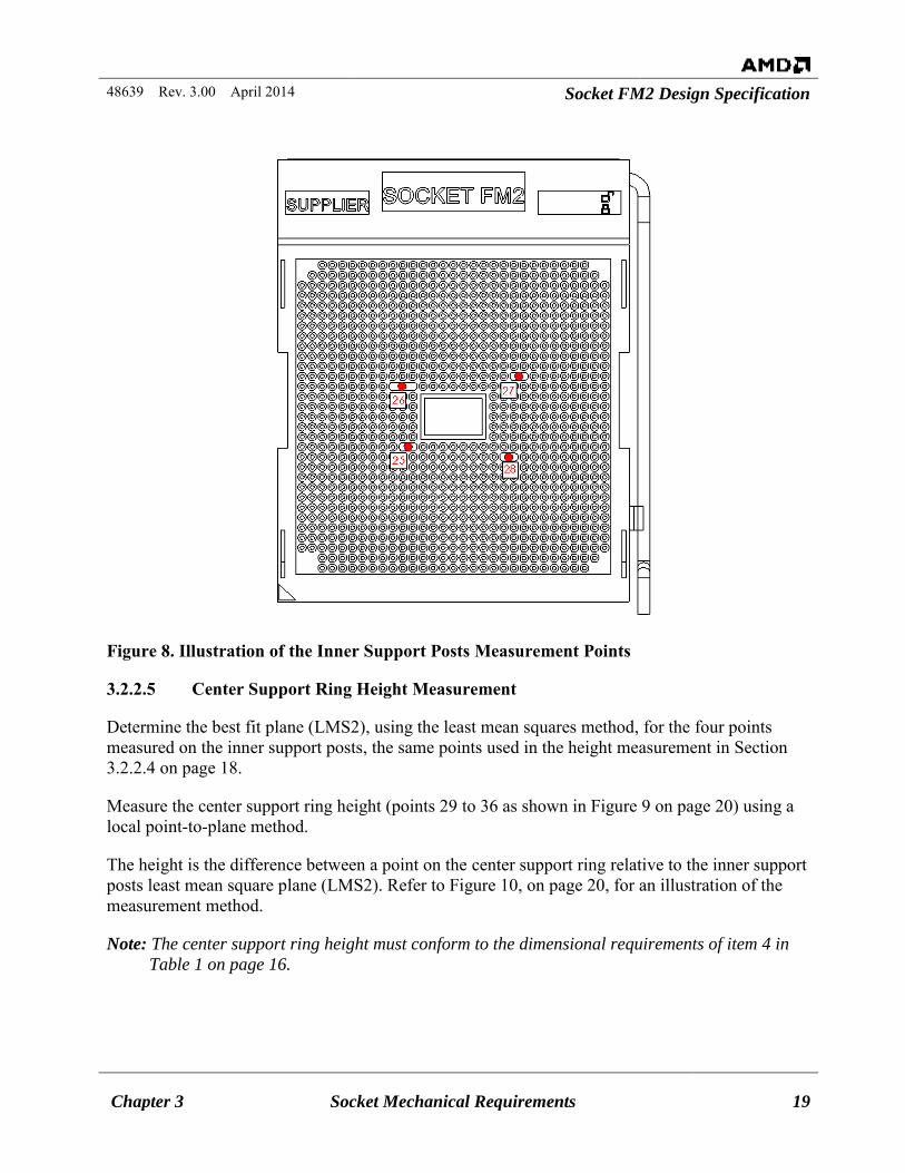
3.2.2.4 Inner Support Posts Height Measurement
Measure the four inner support posts (points 25 to 28 as shown in Figure 8) using a local point-to-plane method.
The height is the difference between a point on the inner support posts relative to the outer support least mean square plane (LMS1). Refer to Figure 10, on page 20, for an illustration of the measurement method.
Note: The inner support posts height must conform to the dimensional requirements of item 3, in
Table 1, on page XXXX16XXXX.
48639 Rev. 3.00 April 2014 Socket FM2 Design Specification
Chapter 3 Socket Mechanical Requirements 19
Figure 8. Illustration of the Inner Support Posts Measurement Points
3.2.2.5 Center Support Ring Height Measurement
Determine the best fit plane (LMS2), using the least mean squares method, for the four points measured on the inner support posts, the same points used in the height measurement in Section X XXX3.2.2.4XXXX on page XXXX18XXXX.
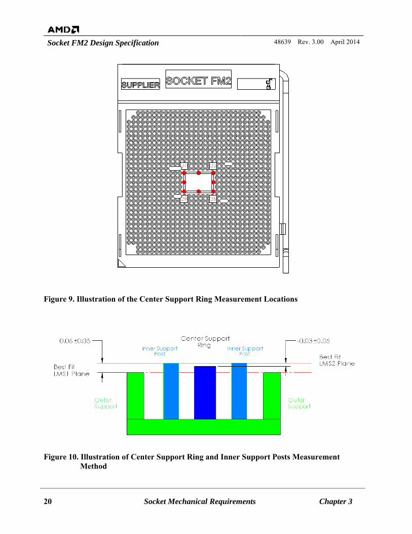
Measure the center support ring height (points 29 to 36 as shown in XXXXFigure 9 XXXX on page XXXX20XXXX) using a local point-to-plane method.
The height is the difference between a point on the center support ring relative to the inner support posts least mean square plane (LMS2). Refer to XXXXFigure 10 XXXX, on page XXXX20 XXXX, for an illustration of the measurement method.
Note: The center support ring height must conform to the dimensional requirements of item 4 in
X XXXTable 1XXXX on page X XXX16XXXX.
Socket FM2 Design Specification 48639 Rev. 3.00 April 2014
20 Socket Mechanical Requirements Chapter 3
Figure 9. Illustration of the Center Support Ring Measurement Locations
Figure 10. Illustration of Center Support Ring and Inner Support Posts Measurement Method
48639 Rev. 3.00 April 2014 Socket FM2 Design Specification
Chapter 3 Socket Mechanical Requirements 21
3.3 Socket Base and Socket Cover The socket base and socket cover are made from liquid crystal polymer (LCP) with a UL flammability rating of 94 V-0. The colors for the socket base and cover are as follows:
Socket base color — black Socket cover color — natural or ivory The thickness of the socket cover (including the 0.30-mm pocket recess) must not exceed 1.17 mm. The socket cover flatness must be less than 0.25 mm before and after the SMT reflow to the PCB. The flatness measurement must be less than 0.25 mm after environmental and mechanical testing.
Either a removable tape or plastic cover acts as an overlay for the pinholes in the top of the socket cover. The overlay facilitates socket pick-and-place operation with a vacuum nozzle during board assembly. The overlay must not outgas during the solder reflow processes or leave any residue upon removal prior to package pins insertion.
3.3.1 Socket Cover Hole
The socket cover pin holes must have a diameter greater than 0.48 mm. The socket cover pin holes must have a pattern relating true position of less than 0.25 mm, and a feature relating true position of less than 0.13mm.
3.3.2 Socket Cover Finger Access
The socket cover must incorporate finger-access cut-outs as shown in Figure 1 on page 10. The cut outs must be at least 8.8 mm long. The center-line of the cutouts must not be off-set from the center line of the socket cover pin-hole array by more than 2.5 mm.
3.3.3 Socket Markings
The requirements for socket markings are as follows:
The socket identifier marking “SOCKET FM2” must be molded into the top surface of the socket cover cam box region. See XXXXFigure 1 XXXX on page X XXX10XXXX.
A locked and unlocked directional designator is molded into the top surface of the cam box in close proximity to the actuation lever. See XXXXFigure 1 XXXX on page XXXX10XXXX.
A triangular shape symbol must be molded into the top of the socket cover for proper package pin A01 orientation. This orientation symbol is located to remain visible after the package is mated to the socket as shown in XXXXFigure 1 XXXX on page XXXX10XXXX and XXXXFigure 3 XXXX on page XXXX14XXXX.
The supplier’s trademark symbol must be molded on the socket cover. Locate this marking to allow visibility and readability after the socket is solder mounted onto the PCB.
The lot traceability number can be ink, laser, or impact marked on the socket cover. Locate the marking to be visible and readable after the socket is solder mounted onto the PCB.
Socket FM2 Design Specification 48639 Rev. 3.00 April 2014
22 Socket Mechanical Requirements Chapter 3
3.4 Socket Contact This section describes the contact material and solder balls for socket attachment to the PCB.
Note: No lubricants can be present on the contact mating areas of fully assembled sockets that
are shipped to customers by the supplier.
3.4.1 Contact Base Metal
The contact base metal is made of high-strength copper alloy.
3.4.2 Contact Plating
The specifications for the contact plating are as follows:
The entire contact is plated with 1.27-μm minimum thickness of nickel. The contact mating area is plated with 0.25-µm minimum thickness of gold over the 1.27 µm
minimum thickness of nickel underplating. Gold porosity in the contact mating areas must be monitored, with no more than two pores with a diameter greater than 0.05 mm allowed per set of 25 contacts examined.
3.4.3 Surface Mount Technology (SMT) Solder Balls
The specifications for the surface mount technology (SMT) solder balls are as follows:
The socket is mounted to the PCB by SMT. The PCB solder pad diameter is 0.56 mm. The solder balls on the socket have a diameter of 0.76 ± 0.15 mm (or AMD approved solder
ball diameter) and are of a lead-free composition. Lead-free solder ball composition can be Sn4.0Ag0.5Cu (SAC405), Sn3.0Ag0.5Cu (SAC305),
or Sn3.5Ag. The contact must include a solder barrier feature to prevent solder from wicking up into the
contact mating area during solder reflow. The Socket FM2 solder ball field must meet the co-planarity requirement of 0.20 mm. Before SMT reflow to PCB, the force required to extract the solder ball from the contact must
be a minimum of: 0.75 kgf shear force for the reflow attached type contact to solder ball interface,
or 0.010 kgf retention force for mechanical attached type contact to solder ball interface.
3.5 Socket Actuation Lever The socket incorporates a lever to the right side of the cam box for actuating and deactuating the socket contacts with the package pins. This actuation lever provides the mechanical advantage to
48639 Rev. 3.00 April 2014 Socket FM2 Design Specification
Chapter 3 Socket Mechanical Requirements 23
easily actuate the socket in an OEM high-volume manufacturing environment and also facilitates tool-less socket actuation and deactuation operations by the end-user.
3.5.1 Lever Material
The recommended material for the actuation lever is stainless steel.
3.5.2 Package Insertion and Extraction Force
With the actuation lever in the open position, the package insertion and extraction forces, conceptually, are zero. These insertion and extraction forces must not exceed 0.075 kgf in actual applications.
3.5.3 Socket Retention Force
With the actuation lever in the closed position, the force required to extract the package pins out of the socket contacts must be a minimum of 0.013 kgf per pin.
3.5.4 Locking Latch
The socket cover incorporates a latch mechanism to lock the lever in the closed position after the socket contacts are mated with the package pins. Support tab(s) are added to the socket cover to cradle the actuation lever in the closed position. The tab(s) prevent the actuation lever from contacting the PCB.
3.5.5 Lever Actuation and Deactuation Force
The force required to actuate or deactuate the lever must be less than 3.6 kgf.
3.5.6 Pin Field Actuation Displacement
The package pins must be displaced less than 1.0 mm during socket actuation or deactuation.
3.6 Socket Durability The socket must maintain electrical and mechanical integrity after 50 actuation and deactuation cycles with each mating package used no more than 5 mating cycles.
3.7 Visual Inspection All visual inspections must be at 1X magnification, except for solder balls that must be inspected at 5X magnification.
3.7.1 Solder Balls
No missing, malformed, damaged, or misaligned solder balls attached to the contacts are allowed.
Socket FM2 Design Specification 48639 Rev. 3.00 April 2014
24 Socket Mechanical Requirements Chapter 3
3.7.2 Contacts
No missing or damaged contacts that prevent the socket from functioning properly are allowed. Contact mating surface must not be missing gold plating.
3.7.3 Cover and Base
No cracks or flashing visible on the socket cover and base are allowed. All tabs that secure the socket cover to the base must not be damaged or missing. The socket cover must fit properly on the socket base with no visible gap between them. The lever latch cannot be damaged or malformed.
3.7.4 Actuation Lever
The actuation lever cannot be damaged, malformed, or missing.
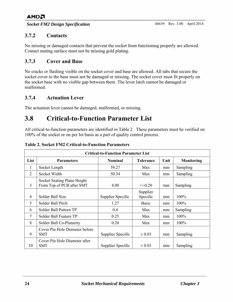
3.8 Critical-to-Function Parameter List All critical-to-function parameters are identified in X XXTable 2XXX XXX. These parameters must be verified on 100% of the socket or on per lot basis as a part of quality control process.
Table 2. Socket FM2 Critical-to-Function Parameters
Critical-to-Function Parameter List
List Parameters Nominal Tolerance Unit Monitoring 1 Socket Length 59.27 Max mm Sampling 2 Socket Width 50.34 Max mm Sampling
3 Socket Seating Plane Height From Top of PCB after SMT 4.00 +/-0.20 mm Sampling
4 Solder Ball Size Supplier Specific Supplier Specific mm 100%
5 Solder Ball Pitch 1.27 Basic mm 100% 6 Solder Ball Pattern TP 0.4 Max mm Sampling 7 Solder Ball Feature TP 0.25 Max mm 100% 8 Solder Ball Co-Planarity 0.20 Max mm 100%
9 Cover Pin Hole Diameter before SMT Supplier Specific ± 0.03 mm Sampling
10 Cover Pin Hole Diameter after SMT Supplier Specific ± 0.03 mm Sampling
48639 Rev. 3.00 April 2014 Socket FM2 Design Specification
Chapter 3 Socket Mechanical Requirements 25
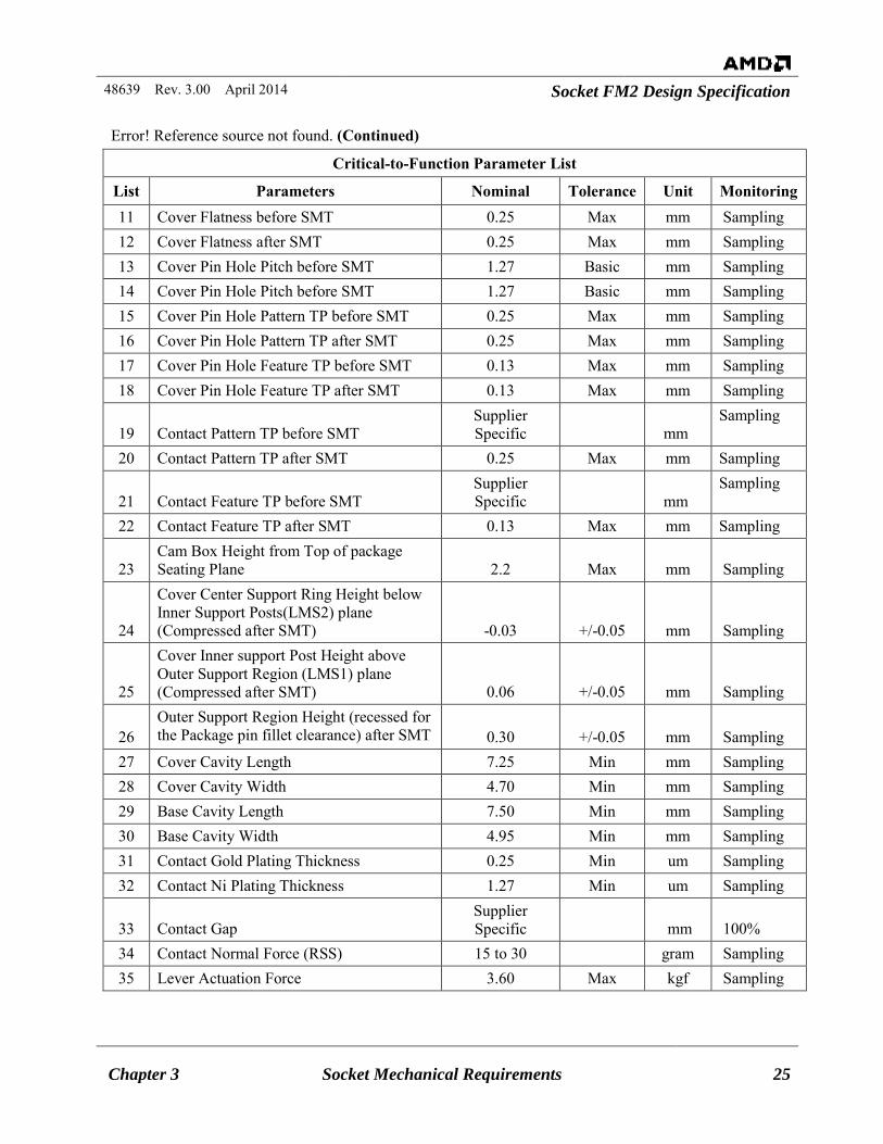
Error! Reference source not found. (Continued)
Critical-to-Function Parameter List
List Parameters Nominal Tolerance Unit Monitoring 11 Cover Flatness before SMT 0.25 Max mm Sampling 12 Cover Flatness after SMT 0.25 Max mm Sampling 13 Cover Pin Hole Pitch before SMT 1.27 Basic mm Sampling 14 Cover Pin Hole Pitch before SMT 1.27 Basic mm Sampling 15 Cover Pin Hole Pattern TP before SMT 0.25 Max mm Sampling 16 Cover Pin Hole Pattern TP after SMT 0.25 Max mm Sampling 17 Cover Pin Hole Feature TP before SMT 0.13 Max mm Sampling 18 Cover Pin Hole Feature TP after SMT 0.13 Max mm Sampling
19 Contact Pattern TP before SMT Supplier Specific mm
Sampling
20 Contact Pattern TP after SMT 0.25 Max mm Sampling
21 Contact Feature TP before SMT Supplier Specific mm
Sampling
22 Contact Feature TP after SMT 0.13 Max mm Sampling
23 Cam Box Height from Top of package Seating Plane 2.2 Max mm Sampling
24
Cover Center Support Ring Height below Inner Support Posts(LMS2) plane (Compressed after SMT) -0.03 +/-0.05 mm Sampling
25
Cover Inner support Post Height above Outer Support Region (LMS1) plane (Compressed after SMT) 0.06 +/-0.05 mm Sampling
26 Outer Support Region Height (recessed for the Package pin fillet clearance) after SMT 0.30 +/-0.05 mm Sampling
27 Cover Cavity Length 7.25 Min mm Sampling 28 Cover Cavity Width 4.70 Min mm Sampling 29 Base Cavity Length 7.50 Min mm Sampling 30 Base Cavity Width 4.95 Min mm Sampling 31 Contact Gold Plating Thickness 0.25 Min um Sampling 32 Contact Ni Plating Thickness 1.27 Min um Sampling
33 Contact Gap Supplier Specific mm 100%
34 Contact Normal Force (RSS) 15 to 30 gram Sampling 35 Lever Actuation Force 3.60 Max kgf Sampling
Socket FM2 Design Specification 48639 Rev. 3.00 April 2014
26 Socket Electrical Requirements Chapter 4
Chapter 4 Socket Electrical Requirements
This chapter describes the contact current rating, inductance, capacitance, differential impedance, propagation delay, cross talk, dielectric withstanding voltage, and insulation resistance of the Socket FM2.
4.1 Contact Current Rating The contact must be rated at a current rating of 1.5 A per contact with less than 30°C temperature rise and with a minimum of ten rows of mated contacts and pins energized.
4.2 Low Level Circuit Resistance (LLCR) Contact resistance applies to the mounted socket with actuated package pin and includes the bulk resistance of the contact, solder ball, package pin, and the interface resistance between the contact and the package pin, but does not include the package internal trace resistance.
4.2.1 Initial Resistance
Initial contact resistance must be measured immediately after the first mating of the package pins to the socket contacts. The 450 daisy-chained pairs (900 contact locations) must be measured per socket sample. Initial LLCR must not exceed 20 mΩ per contact when mated with Cu Alloy-194 pins, based on measurements made on a daisy-chained pair of contacts.
4.2.2 Final Resistance
Final contact resistance must be measured after the mechanical and environmental testing of the mated package and socket is complete. The same 450 daisy-chained pairs (900 contact locations) must be measured per socket sample. Final LLCR must not exceed 20 mΩ per contact when mated with Cu Alloy-194 pins, based on measurements made on a daisy-chained pair of contacts.
4.3 Inductance The inductance specifications for the Socket FM2 are as follows:
The mated, partial self-inductance of a single pin must be less than 4 nH. The mated-loop inductance of two nearest pins must be less than 3.3 nH. The mated partial-loop inductance matrix of three neighboring pins must be less than 3.3 nH
for the diagonal entries, and must be less than 2.2 nH for the off-diagonal entries.
Note: Measurements are made at frequencies of 500 MHz and 2 GHz.
48639 Rev. 3.00 April 2014 Socket FM2 Design Specification
Chapter 4 Socket Electrical Requirements 27
4.4 Capacitance The capacitance specifications for the Socket FM2 are as follows:
The mated capacitance between two nearest pins must be less than 1 pF. The mated capacitance matrix of three neighboring pins must be less than 1 pF.
Note: Measurements are made at frequencies of 500 MHz and 2 GHz.
4.5 Differential Impedance The differential (or odd mode) impedance for three, mated-pins configuration (one pin as the voltage/current reference—S1, S2, and G) must be 100 Ω ± 10% between the two nearest pins (with an additional ± 2-Ω measurement error). If the Time Domain Method is used, the signal must have a rise time of 150 ps for the signal amplitude to go from 10% to 90%.
4.6 Propagation Delay The propagation delay specifications for the Socket FM2 are as follows:
The propagation delay skew among single-ended signals must be less than 10 ps, plus a maximum measurement error of 3 ps.
The propagation delay skew among differential signal pairs must be less than 10 ps, plus a maximum measurement error of 3 ps.
4.7 Cross Talk Cross talk between the nearest single-ended and differential signals must be measured and compared to results from the measured partial-loop inductance and the Maxwell capacitance matrices.
4.8 Dielectric Withstanding Voltage (DWV) The contact-to-contact dielectric withstanding voltage between randomly selected adjacent lateral, diagonal, and vertical contacts must be a minimum of 650 VAC.
4.9 Insulation Resistance (IR) The contact-to-contact insulation resistance between randomly selected adjacent lateral, diagonal, and vertical contacts must be a minimum of 1000 MΩ.
Socket FM2 Design Specification 48639 Rev. 3.00 April 2014
28 Socket Environmental Requirements Chapter 5
Chapter 5 Socket Environmental Requirements
This section describes the socket design required to meet reliability requirements for the end-user field-use environment, OEM high volume manufacturing environment, and shipping and handling conditions of desktop computers.
5.1 Thermal Shock Sockets must meet LLCR and visual inspection requirements after being subjected to 10 thermal shock cycles with the cold temperature extreme at –55°C and the hot temperature extreme at +110°C. The dwell at each temperature extreme is 30 minutes with less than 15 seconds transition time. The test should be conducted with the associated heatsink assembly (AMD part number 7120038000G) attached to the processor package.
5.2 Cyclic Humidity Sockets must meet low-level circuit resistance (LLCR), dielectric withstanding voltage (DWV), insulation resistance (IR), and visual inspection requirements after being subjected to 1000 hours of cyclic humidity tests with a cycle time of eight hours. Temperature range is 25°C to 85°C with relative humidity maintained between 90% to 95%. This test should be conducted with the associated heatsink assembly (AMD part number 7120038000G) attached to the processor package.
5.3 Thermal Cycling Sockets must meet LLCR and visual inspection requirements after being subjected to a minimum of 1000 cycles of thermal cycles with testing continued until 60% of the sockets fail or 3000 cycles are completed. Cold temperature extreme is –55°C with a dwell time of 20 minutes, and hot temperature extreme is +110°C with a dwell time of 15 minutes. The average rate of temperature change between the hot and cold temperature extremes must not exceed 10°C per minute. This test should be conducted with the associated heatsink assembly (AMD part number 7120038000G) attached to the processor package.
5.4 Temperature Life Sockets must meet LLCR and visual inspection requirements after being subjected to 500 hours of temperature life testing at 115°C. This test should be conducted with the associated heatsink assembly (AMD part number 7120038000G) attached to the processor package.

48639 Rev. 3.00 April 2014 Socket FM2 Design Specification
Chapter 5 Socket Environmental Requirements 29
5.5 Industrial Mixed Flowing Gas Sockets must meet LLCR and visual inspection requirements after being subjected to mixed flowing gas testing with half the samples mated and the other half samples unmated for the first five days, and then all samples mated for the final five days. The test temperature is 30°C with a relative humidity of 70%. Mixed flowing gas constituents are 10-ppb chlorine, 10-ppb hydrogen sulfide, 200-ppb nitrogen dioxide, and 100-ppb sulfur dioxide.
5.6 Mechanical Shock Sockets must meet LLCR, continuity intermittency of less than 1-μs duration, and visual inspection requirements after being subjected to mechanical shock testing at 50 g, 11-ms duration, half-sine waveform with three shocks per positive and negative directions on all three axes — totaling 18 shocks. This test should be conducted with the associated heatsink assembly (AMD part number 7120038000G) attached to the processor package.
5.7 Random Vibration Sockets must meet LLCR, continuity intermittency of less than 1-μs duration, and visual inspection requirements after being subjected to random vibration testing at 3.1 g rms between 20 Hz to 500 Hz for duration of 45 minutes per axis for each of the three axes. This test should be conducted with the associated heatsink assembly (AMD part number 7120038000G) attached to the processor package.
5.8 Resistance to Solder Heat Sockets must meet LLCR, cover flatness, and visual inspection requirements after being subjected to four convection-solder-reflow processes for mounting the socket to the PCB. No deterioration of the markings on the socket is allowed.
5.9 Resistance to Solvents Sockets must meet visual inspection requirements after being subjected to the Four Solutions test. No deterioration of the markings on the socket is allowed.
5.10 Heatsink Assembly The associated heatsink assembly (AMD part number 7120038000G) attached to the processor package in the environmental testing can weigh up to 450 grams.