sns college of engineering ec8691-microprocessors and
TRANSCRIPT
SNS COLLEGE OF ENGINEERING
EC8691-Microprocessors and Microcontrollers IAE -1 ANSWER KEY
PART A - (10 X 1 = 10 marks)
1. 8086 is a _____ bit
(a) 8 (b) 16 (c) 32 (d) 64
2. Formula for physical address =
(a) Stack *10 + offset (b) pointer * 10 + offset (c) stack * 10 -offset (d) stack -10 + offset
3. The basic memory unit is
(a) bit (b) byte (c) address (d) pointer
4. 8086 supports ____________ memory
(a)bit addressable (b) byte addressable (c) immediate address (d)
direct address
5. All conditional jump instructions can be used within approximately bytes
from current instruction.
(a) +117 to -117 (b) +127 to-127 (c) +217 to -217 (d) +327 to -327
6. Formula for memory address: Memory address =
(a) start address of memory segment + offset (b) end address of memory segment
+ offset (c) start address of memory segment + pointer (d) Pointer + offset
7. Abbreviation of DAA
(a) Design Adjust for Addition (b) Decimal Adjust for Addition (c) Decimal Addition
for Adjust (d) Design Address for Addition
8. A set of conductors used for communicating information between the components in a
computer is called a
(a) bus (b) address (c) index (d) pin
9 The movement of information between the CPU and memory is considered as
(a) modular programming (b) I/O programming (c) assembler programming
(d) architectural programming
10. Which is used for monitor storage
(a) RAM (b) EPROM (c) EEPROM (d) ROM
PART A - (10 X 2 = 20 marks)
11. Examine the effect of executing the instruction DAD and ADD M?
DAD is a mnemonic, which stands for Double ADD
ADD M AC←AC + hxi 00000011 Add memory contents at M to AC
12. Draw the contents of the flag register 8086.
The flag register is one of the special purpose register. The flag bits are changed to 0 or 1
depending upon the value of result after arithmetic or logical operations.
8086 has 16-bit flag register, and there are 9 valid flag bits. The format of flag register is like
below.

SNS COLLEGE OF ENGINEERING
EC8691-Microprocessors and Microcontrollers IAE -1 ANSWER KEY
Bits D15 D14 D13 D12 D11 D10 D9 D8 D7 D6 D5 D4 D3 D2 D1 D0
Flags O D I T S Z AC P CY
We can divide the flag bits into two sections. The Status Flags, and the Control Flags.
(or)
13. Name the hardware interrupts of 8086.
14. Compare microprocessor and microcontroller?
Sl.no Microprocessor Microcontroller
1 General purpose processor Specific application controller
2 Contains no RAM, no ROM, no I/O ports on
chip itself.
Contains RAM, ROM, I/O ports on chip
itself
3 Size of RAM/ROM can vary Size of RAM/ROM is fixed
4 Makes the system bulkier Make the system compact
5 More expensive Less expensive
6 It has less bit handling instructions It has more bit handling instructions
7 Less number of pins have multiplexed
functions
more number of pins have multiplexed
functions
8 More flexible in designer point of view Less flexible in designer point of view
9 Limited power saving options compared to
microcontrollers
Includes lot of power saving features

SNS COLLEGE OF ENGINEERING
EC8691-Microprocessors and Microcontrollers IAE -1 ANSWER KEY
10 Eg: Desktop PC,8086,i7 Eg: Digital Camera,8051,msp430
11 Execution faster Compared to µp slower
12 More general purpose registers Less number of gen purpose registers
13 More addressing modes Less addressing modes
14 Design time is more Application design time less
15 Microprocessors are based on von
Neumann model/architecture where
program and data are stored in same
memory module
Micro controllers are based on Harvard
architecture where program memory and
Data memory are
separate
16 Cannot be used in compact systems and
hence inefficient
Can be used in compact systems and
hence it is an efficient technique
17 Example code: Example code:
ADD AX,BX MOV A,#2fh
ADD AX,CX MOV B,#2fh
ADD AX,DX ADD A,B
18 It cannot be used as stand alone Can be used as stand alone.
19 May or may not be real-time application
oriented
Real-time application oriented
20 Fig : a Fig :b
Fig
: (a) Microprocessor Fig : (b) Microcontroller
Definition: µP - silicon chip representing CPU which is capable of performing arithmetic as well
as logical operations.
Definition: µc - highly integrated chip that contains a CPU, scratch pad RAM, special and general
purpose register array, on-chip ROM, Flash memory for program storage, Timer and interrupt
control unit and dedicated IO ports.
15. What do you mean by addressing modes?
The addressing mode is the method to specify the operand of an instruction. The job of a
microprocessor is to execute a set of instructions stored in memory to perform a specific task.
Operations require the following:
The operator or opcode which determines what will be done
The operands which define the data to be used in the operation

SNS COLLEGE OF ENGINEERING
EC8691-Microprocessors and Microcontrollers IAE -1 ANSWER KEY
For example, if we wanted to add the numbers 1 and 2 and get a result, mathematically
we would likely write this as 1 + 2. In this case, our operator is (+), or the addition, and our
operands are the numbers 1 and 2.
16. Justify the processing element inside the microprocessor? What process it does?
The microprocessor contains all, or most of, the central processing unit (CPU) functions and is
the "engine" that goes into motion when you turn your computer on. A microprocessor is
designed to perform arithmetic and logic operations that make use of small number-holding
areas called registers
17. How many locations can be addressed by 8086 microprocessor?
8086 has a 20 bit address bus can access upto 220 memory locations ( 1 MB) . It can support
upto 64K I/O ports. It provides 14, 16-bit registers
18. Differentiate minimum and maximum mode.
Maximum mode Minimum Mode
When MN/MX(bar) low 8086 is in maximum mode.
When MN/MX(bar) high 8086 is in minimum mode.
In maximum mode 8086 generates QS1,QS0,S0(bar),S1(bar),S2(bar), LOCK(bar),RQ(bar)/GT1,RQ(bar)/GT0 control signals
In minimum mode 8086 generates INTA(bar), ALE, DEN(bar), DT/R(bar), M/IO(bar), HLDA,HOLD and WR(bar) control signals.
So clearly there are multiple processors in the system.
There is only one processor in the system minimum mode.
Whereas in maximum mode interfacing, master/slave and multiplexing and several such control signals are required In maximum mode a bus controller is required to produce control signals. This bus controller produces MEMRDC, MEMWRC, IORDC, IOWRC, ALE, DEN, DT/R control signals.
In minimum mode no interfacing or master/slave signals is required. In minimum mode direct RD WR signals can be used. No bus controller required. A simple demultiplexer would do the job. of producing the control signals. This demultiplexer produces MEMRD, MEMWR, IORD, IOWR control signals.

SNS COLLEGE OF ENGINEERING
EC8691-Microprocessors and Microcontrollers IAE -1 ANSWER KEY
19. Give any four pin definitions for maximum mode.
Pin configuration of 8086
Power supply and frequency signals
It uses 5V DC supply at VCC pin 40, and uses ground at VSS pin 1 and 20 for its operation.
Clock signal
Clock signal is provided through Pin-19. It provides timing to the processor for operations. Its
frequency is different for different versions, i.e. 5MHz, 8MHz and 10MHz.
QS1 and QS0
These are queue status signals and are available at pin 24 and 25. These signals provide the
status of instruction queue. Their conditions are shown in the following table −
QS0 QS1 Status
0 0 No operation
0 1 First byte of opcode from the queue
1 0 Empty the queue
1 1 Subsequent byte from the queue
20. What is pipelining?
Pipelining is the process of accumulating and executing computer instructions and tasks from
the processor via a logical pipeline. It allows storing, prioritizing, managing and executing tasks
and instructions in an orderly process. Pipelining is also known as pipeline processing.

SNS COLLEGE OF ENGINEERING
EC8691-Microprocessors and Microcontrollers IAE -1 ANSWER KEY
PART B - (5 X 14 = 70 marks)
21. (a) Explain 8086 architecture in detail.
Architecture of 8086
A Microprocessor is an Integrated Circuit with all the functions of a CPU however; it cannot be
used stand alone since unlike a microcontroller it has no memory or peripherals.
8086 does not have a RAM or ROM inside it. However, it has internal registers for storing
intermediate and final results and interfaces with memory located outside it through the System
Bus.
In case of 8086, it is a 16-bit Integer processor in a 40 pin, Dual Inline Packaged IC.
The size of the internal registers(present within the chip) indicate how much information the
processor can operate on at a time (in this case 16-bit registers) and how it moves data around
internally within the chip, sometimes also referred to as the internal data bus.
8086 provides the programmer with 14 internal registers, each 16 bits or 2 Bytes wide.
Memory segmentation:
To increase execution speed and fetching speed, 8086 segments the memory.
It’s 20 bit address bus can address 1MB of memory, it segments it into 4 64kB segments.
8086 works only with four 64KB segments within the whole 1MB memory.
The internal architecture of Intel 8086 is divided into 2 units: The Bus Interface Unit (BIU), and
The Execution Unit (EU). These are explained as following below.
1. The Bus Interface Unit (BIU):

SNS COLLEGE OF ENGINEERING
EC8691-Microprocessors and Microcontrollers IAE -1 ANSWER KEY
It provides the interface of 8086 to external memory and I/O devices via the System Bus.
It performs various machine cycles such as memory read, I/O read etc. to transfer data between
memory and I/O devices.
BIU performs the following functions-
It generates the 20 bit physical address for memory access.
It fetches instructions from the memory.
It transfers data to and from the memory and I/O.
Maintains the 6 byte prefetch instruction queue(supports pipelining).
BIU mainly contains the 4 Segment registers, the Instruction Pointer, a prefetch queue and
an Address Generation Circuit.
Instruction Pointer (IP):
It is a 16 bit register. It holds offset of the next instructions in the Code Segment.
IP is incremented after every instruction byte is fetched.
IP gets a new value whenever a branch instruction occurs.
CS is multiplied by 10H to give the 20 bit physical address of the Code Segment.
Address of the next instruction is calculated as CS x 10H + IP.
Example:
CS = 4321H IP = 1000H
then CS x 10H = 43210H + offset = 53210H
This is the address of the instruction.
Code Segment register:
CS holds the base address for the Code Segment. All programs are stored in the Code Segment
and accessed via the IP.
Data Segment register:
DS holds the base address for the Data Segment.
Stack Segment register:
SS holds the base address for the Stack Segment.
Extra Segment register:
ES holds the base address for the Extra Segment.
Address Generation Circuit:
The BIU has a Physical Address Generation Circuit.
It generates the 20 bit physical address using Segment and Offset addresses using the formula:
Physical Address = Segment Address x 10H + Offset Address
6 Byte Pre-fetch Queue:
It is a 6 byte queue (FIFO).
Fetching the next instruction (by BIU from CS) while executing the current instruction is called
pipelining.
Gets flushed whenever a branch instruction occurs.
2. The Execution Unit (EU):
The main components of the EU are General purpose registers, the ALU, Special purpose
registers, Instruction Register and Instruction Decoder and the Flag/Status Register.

SNS COLLEGE OF ENGINEERING
EC8691-Microprocessors and Microcontrollers IAE -1 ANSWER KEY
Fetches instructions from the Queue in BIU, decodes and executes arithmetic and logic
operations using the ALU.
Sends control signals for internal data transfer operations within the microprocessor.
Sends request signals to the BIU to access the external module.
It operates with respect to T-states (clock cycles) and not machine cycles.
8086 has four 16 bit general purpose registers AX, BX, CX and DX. Store intermediate values
during execution. Each of these have two 8 bit parts (higher and lower).
AX register:
It holds operands and results during multiplication and division operations. Also an accumulator
during String operations.
BX register:
It holds the memory address (offset address) in indirect addressing modes.
CX register:
It holds count for instructions like loop, rotate, shift and string operations.
DX register:
It is used with AX to hold 32 bit values during multiplication and division.
Arithmetic Logic Unit (16 bit):
Performs 8 and 16 bit arithmetic and logic operations.
Special purpose registers (16-bit):
Stack Pointer:
Points to Stack top. Stack is in Stack Segment, used during instructions like PUSH, POP, CALL, RET
etc.
Base Pointer:
BP can hold offset address of any location in the stack segment. It is used to access random
locations of the stack.
Source Index:
It holds offset address in Data Segment during string operations.
Destination Index:
It holds offset address in Extra Segment during string operations.
Instruction Register and Instruction Decoder:
The EU fetches an opcode from the queue into the instruction register. The instruction decoder
decodes it and sends the information to the control circuit for execution.
Flag/Status register (16 bits):
It has 9 flags that help change or recognize the state of the microprocessor.
6 Status flags:
carry flag(CF)
parity flag(PF)
auxiliary carry flag(AF)
zero flag(Z)
sign flag(S)
Status flags are updated after every arithmetic and logic operation.

SNS COLLEGE OF ENGINEERING
EC8691-Microprocessors and Microcontrollers IAE -1 ANSWER KEY
3 Control flags:
trap flag(TF)
interrupt flag(IF)
direction flag(DF)
These flags can be set or reset using control instructions like CLC, STC, CLD, STD, CLI, STI, etc.
The Control flags are used to control certain operations.
(b) Explain linking and relocation with neat diagram.
Linking and Relocation
The DOS linking program links the different object modules of a source program and
function library routines to generate an integrated executable code of the source program. The
main input to the linker is the .OBJ file that contains the object modules of the source programs.
Other supporting information may be obtained from the files generated by the MASM. The
linker program is invoked using the following options.
C> LINK or
C>LINK MS.OBJ
The .OBJ extension is a must for a file to be accepted by the LINK as a valid object file. The first
object may generate a display asking for the object file, list file and libraries as inputs and an
expected name of the .EXE file to be generated. The output of the link program is an executable
file with the entered filename and .EXE extension. This executable filename can further be
entered at the DOS prompt to execute the file.
In the advanced version of the MASM, the complete procedure of assembling and linking is
combined under a single menu invokable compile function. The recent versions of MASM have
much more sophisticated and user-friendly facilities and options. A linker links the machine
codes with the other required assembled codes. Linking is necessary because of the number of
codes to be linked for the final binary file.
The linked file in binary for run on a computer is commonly known as executable file or simply
‘.exe.’ file. After linking, there has to be re-allocation of the sequences of placing the codes
before actually placement of the codes in the memory.
The loader program performs the task of reallocating the codes after finding the physical RAM
addresses available at a given instant. The DOS linking program links the different object
modules of a source program and function library routines to generate an integrated executable
code of the source program. The main input to the linker is the .OBJ file that contains the object
modules of the source programs. Other supporting information may be obtained from the files
generated by the MASM. The linked file in binary for run on a computer is commonly known as
executable file or simply ‘.exe.’ file. After linking, there has to be re-allocation of the sequences
of placing the codes before actually placement of the codes in the memory.
The loader program performs the task of reallocating the codes after finding the physical RAM
addresses available at a given instant. The loader is a part of the operating system and places
codes into the memory after reading the ‘.exe’ file. This step is necessary because the available
memory addresses may not start from 0x0000, and binary codes have to be loaded at the

SNS COLLEGE OF ENGINEERING
EC8691-Microprocessors and Microcontrollers IAE -1 ANSWER KEY
different addresses during the run. The loader finds the appropriate start address. In a
computer, the loader is used and it loads into a section of RAM the program that is ready to run.
A program called locatorreallocates the linked file and creates a file for permanent location of
codes in a standard format.
Segment combination
In addition to the linker commands, the assembler provides a means of regulating the way
segments in different object modules are organized by the linker. Segments with same name are
joined together by using the modifiers attached to the SEGMENT directives. SEGMENT directive
may have the form Segment name SEGMENT Combination-type where the combine-type
indicates how the segment is to be located within the load module. Segments that have
different names cannot be combined and segments with the same name but no combine-type
will cause a linker error. The possible combine-types are:
PUBLIC – If the segments in different modules have the same name and combine-type
PUBLIC, then they are concatenated into a single element in the load module. The ordering in
the concatenation is specified by the linker command.
COMMON – If the segments in different object modules have the same name and the
combine-type is COMMON, then they are overlaid so that they have the same starting address.
The length of the common segment is that of the longest segment being overlaid.
STACK – If segments in different object modules have the same name and the combine
type STACK, then they become one segment whose length is the sum of the lengths of the
individually specified segments. In effect, they are combined to form one large stack
AT – The AT combine-type is followed by an expression that evaluates to a
constant which is to be the segment address. It allows the user to specify the exact location of
the segment in memory.
MEMORY – This combine-type causes the segment to be placed at the last of the
load module. If more than one segment with the MEMORY combine-type is being linked, only
the first one will be treated as having the MEMORY combine type; the others will be overlaid as
if they had COMMON combine-type.

SNS COLLEGE OF ENGINEERING
EC8691-Microprocessors and Microcontrollers IAE -1 ANSWER KEY
Fig. 1.9 Segment combinations resulting from the PUBLIC and Common Combination types
Access to External Identifiers
If an identifier is defined in an object module, then it is said to be a local (or internal)
identifier relative to the module. If it is not defined in the module but is defined in one of the
other modules being linked, then it is referred to as an external (or global) identifier relative to
the module. In order to permit other object modules to reference some of the identifiers in a
given module, the given module must include a list of the identifiers to which it will allow
access. Therefore, each module in multi-module programs may contain two lists, one containing
the external identifiers that can be referred to by other modules. Two lists are implemented by
the EXTRN and PUBLIC directives, which have the forms:

SNS COLLEGE OF ENGINEERING
EC8691-Microprocessors and Microcontrollers IAE -1 ANSWER KEY
where the identifiers are the variables and labels being declared or as being available to other
modules. The assembler must know the type of all external identifiers before it can generate
the proper machine code, a type specifier must be associated with each identifier in an EXTRN
statement. For a variable the type may be BYTE, WORD, or DWORD and for a label it may be
NEAR or FAR.
One of the primary tasks of the linker is to verify that every identifier appearing in an
EXTRN statement is matched by one in a PUBLIC statement. If this is not the case, then there will
be an undefined reference and a linker error will occur. The offsets for the local identifier will be
inserted by the assembler, but the offsets for the external identifiers and all segment addresses
must be inserted by the linking process. The offsets associated with all external references can
be assigned once all of the object modules have been found and their external symbol tables
have been examined. The assignment of the segment addresses is called relocation and is done
after the linking process has determined exactly where each segment is to be put in memory.
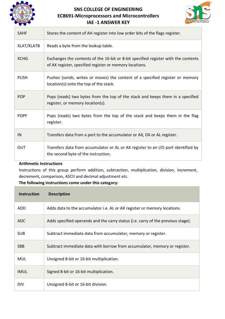
22. (a) Explain instruction sets with example.
Instructions are classified on the basis of functions they perform. They are categorized
into the following main types:
Data Transfer instruction
All the instructions which perform data movement come under this category. The source data
may be a register, memory location, port etc. the destination may be a register, memory
location or port. The following instructions come under this category:
Instruction Description
MOV Moves data from register to register, register to memory, memory to register,
memory to accumulator, accumulator to memory, etc.
LDS Loads a word from the specified memory locations into specified register. It also
loads a word from the next two memory locations into DS register.
LES Loads a word from the specified memory locations into the specified register. It
also loads a word from next two memory locations into ES register.
LEA Loads offset address into the specified register.
LAHF Loads low order 8-bits of the flag register into AH register.
SNS COLLEGE OF ENGINEERING
EC8691-Microprocessors and Microcontrollers IAE -1 ANSWER KEY
SAHF Stores the content of AH register into low order bits of the flags register.
XLAT/XLATB Reads a byte from the lookup table.
XCHG Exchanges the contents of the 16-bit or 8-bit specified register with the contents
of AX register, specified register or memory locations.
PUSH Pushes (sends, writes or moves) the content of a specified register or memory
location(s) onto the top of the stack.
POP Pops (reads) two bytes from the top of the stack and keeps them in a specified
register, or memory location(s).
POPF Pops (reads) two bytes from the top of the stack and keeps them in the flag
register.
IN Transfers data from a port to the accumulator or AX, DX or AL register.
OUT Transfers data from accumulator or AL or AX register to an I/O port identified by
the second byte of the instruction.
Arithmetic Instructions
Instructions of this group perform addition, subtraction, multiplication, division, increment,
decrement, comparison, ASCII and decimal adjustment etc.
The following instructions come under this category:
Instruction Description
ADD Adds data to the accumulator i.e. AL or AX register or memory locations.
ADC Adds specified operands and the carry status (i.e. carry of the previous stage).
SUB Subtract immediate data from accumulator, memory or register.
SBB Subtract immediate data with borrow from accumulator, memory or register.
MUL Unsigned 8-bit or 16-bit multiplication.
IMUL Signed 8-bit or 16-bit multiplication.
DIV Unsigned 8-bit or 16-bit division.

SNS COLLEGE OF ENGINEERING
EC8691-Microprocessors and Microcontrollers IAE -1 ANSWER KEY
IDIV Signed 8-bit or 16-bit division.
INC Increment Register or memory by 1.
DEC Decrement register or memory by 1.
DAA Decimal Adjust after BCD Addition: When two BCD numbers are added, the
DAA is used after ADD or ADC instruction to get correct answer in BCD.
DAS Decimal Adjust after BCD Subtraction: When two BCD numbers are added, the
DAS is used after SUB or SBB instruction to get correct answer in BCD.
AAA ASCII Adjust for Addition: When ASCII codes of two decimal digits are added,
the AAA is used after addition to get correct answer in unpacked BCD.
AAD Adjust AX Register for Division: It converts two unpacked BCD digits in AX to the
equivalent binary number. This adjustment is done before dividing two
unpacked BCD digits in AX by an unpacked BCD byte.
AAM Adjust result of BCD Multiplication: This instruction is used after the
multiplication of two unpacked BCD.
AAS ASCII Adjust for Subtraction: This instruction is used to get the correct result in
unpacked BCD after the subtraction of the ASCII code of a number from ASCII
code another number.
CBW Convert signed Byte to signed Word.
CWD Convert signed Word to signed Doubleword.
NEG Obtains 2's complement (i.e. negative) of the content of an 8-bit or 16-bit
specified register or memory location(s).
CMP Compare Immediate data, register or memory with accumulator, register or
memory location(s).
Logical Instructions
Instruction of this group perform logical AND, OR, XOR, NOT and TEST operations. The following
instructions come under this category:

SNS COLLEGE OF ENGINEERING
EC8691-Microprocessors and Microcontrollers IAE -1 ANSWER KEY
Instruction Description
AND Performs bit by bit logical AND operation of two operands and places the result
in the specified destination.
OR Performs bit by bit logical OR operation of two operands and places the result in
the specified destination.
XOR Performs bit by bit logical XOR operation of two operands and places the result
in the specified destination.
NOT Takes one's complement of the content of a specified register or memory
location(s).
TEST Perform logical AND operation of a specified operand with another specified
operand.
Rotate Instructions
The following instructions come under this category:
Instruction Description
RCL Rotate all bits of the operand left by specified number of bits through carry flag.
RCR Rotate all bits of the operand right by specified number of bits through carry
flag.
ROL Rotate all bits of the operand left by specified number of bits.
ROR Rotate all bits of the operand right by specified number of bits.
Shift Instructions
The following instructions come under this category:
Instruction Description
SAL or SHL Shifts each bit of operand left by specified number of bits and put zero in LSB
position.
SAR Shift each bit of any operand right by specified number of bits. Copy old MSB
into new MSB.

SNS COLLEGE OF ENGINEERING
EC8691-Microprocessors and Microcontrollers IAE -1 ANSWER KEY
SHR Shift each bit of operand right by specified number of bits and put zero in MSB
position.
Branch Instructions
It is also called program execution transfer instruction. Instructions of this group transfer
program execution from the normal sequence of instructions to the specified destination or
target. The following instructions come under this category:
Instruction Description
JA or JNBE Jump if above, not below, or equal i.e. when CF and ZF = 0
JAE/JNB/JNC Jump if above, not below, equal or no carry i.e. when CF = 0
JB/JNAE/JC Jump if below, not above, equal or carry i.e. when CF = 0
JBE/JNA Jump if below, not above, or equal i.e. when CF and ZF = 1
JCXZ Jump if CX register = 0
JE/JZ Jump if zero or equal i.e. when ZF = 1
JG/JNLE Jump if greater, not less or equal i.e. when ZF = 0 and CF = OF
JGE/JNL Jump if greater, not less or equal i.e. when SF = OF
JL/JNGE Jump if less, not greater than or equal i.e. when SF ≠ OF
JLE/JNG Jump if less, equal or not greater i.e. when ZF = 1 and SF ≠ OF
JMP Causes the program execution to jump unconditionally to the memory
address or label given in the instruction.
CALL Calls a procedure whose address is given in the instruction and saves their
return address to the stack.
RET Returns program execution from a procedure (subroutine) to the next
instruction or main program.
IRET Returns program execution from an interrupt service procedure
(subroutine) to the main program.

SNS COLLEGE OF ENGINEERING
EC8691-Microprocessors and Microcontrollers IAE -1 ANSWER KEY
INT Used to generate software interrupt at the desired point in a program.
INTO Software interrupts to indicate overflow after arithmetic operation.
LOOP Jump to defined label until CX = 0.
LOOPZ/LOOPE Decrement CX register and jump if CX ≠ 0 and ZF = 1.
LOOPNZ/LOOPNE Decrement CX register and jump if CX ≠ 0 and ZF = 0.
Here, CF = Carry Flag
ZF = Zero Flag
OF = Overflow Flag
SF = Sign Flag
CX = Register
Flag Manipulation and Processor Control Instructions
Instructions of this instruction set are related to flag manipulation and machine control. The
following instructions come under this category:
Instruction Description
CLC Clear Carry Flag: This instruction resets the carry flag CF to 0.
CLD Clear Direction Flag: This instruction resets the direction flag DF to 0.
CLI Clear Interrupt Flag: This instruction resets the interrupt flag IF to 0.
CMC This instruction take complement of carry flag CF.
STC Set carry flag CF to 1.
STD Set direction flag to 1.
STI Set interrupt flag IF to 1.
SNS COLLEGE OF ENGINEERING
EC8691-Microprocessors and Microcontrollers IAE -1 ANSWER KEY
HLT Halt processing. It stops program execution.
NOP Performs no operation.
ESC Escape: makes bus free for external master like a coprocessor or peripheral
device.
WAIT When WAIT instruction is executed, the processor enters an idle state in which
the processor does no processing.
LOCK It is a prefix instruction. It makes the LOCK pin low till the execution of the next
instruction.
String Instructions
String is series of bytes or series of words stored in sequential memory locations. The 8086
provides some instructions which handle string operations such as string movement,
comparison, scan, load and store.
The following instructions come under this category:
Instruction Description
MOVS/MOVSB/MOVSW Moves 8-bit or 16-bit data from the memory location(s) addressed
by SI register to the memory location addressed by DI register.
CMPS/CMPSB/CMPSW Compares the content of memory location addressed by DI register
with the content of memory location addressed by SI register.
SCAS/SCASB/SCASW Compares the content of accumulator with the content of memory
location addressed by DI register in the extra segment ES.
LODS/LODSB/LODSW Loads 8-bit or 16-bit data from memory location addressed by SI
register into AL or AX register.
STOS/STOSB/STOSW Stores 8-bit or 16-bit data from AL or AX register in the memory
location addressed by DI register.
REP Repeats the given instruction until CX ≠ 0

SNS COLLEGE OF ENGINEERING
EC8691-Microprocessors and Microcontrollers IAE -1 ANSWER KEY
REPE/ REPZ Repeats the given instruction till CX ≠ 0 and ZF = 1
REPNE/REPNZ Repeats the given instruction till CX ≠ 0 and ZF = 0
(b) What are interrupts? Explain the types of interrupts.
Interrupt is the method of creating a temporary halt during program execution and allows
peripheral devices to access the microprocessor. The microprocessor responds to that interrupt
with an ISR (Interrupt Service Routine), which is a short program to instruct the microprocessor
on how to handle the interrupt.
The following image shows the types of interrupts we have in a 8086 microprocessor −
Hardware Interrupts
Hardware interrupt is caused by any peripheral device by sending a signal through a specified
pin to the microprocessor.
The 8086 has two hardware interrupt pins, i.e. NMI and INTR. NMI is a non-maskable interrupt
and INTR is a maskable interrupt having lower priority. One more interrupt pin associated is
INTA called interrupt acknowledge.
NMI
It is a single non-maskable interrupt pin (NMI) having higher priority than the maskable
interrupt request pin (INTR)and it is of type 2 interrupt.
When this interrupt is activated, these actions take place −
Completes the current instruction that is in progress.
Pushes the Flag register values on to the stack.
Pushes the CS (code segment) value and IP (instruction pointer) value of the return
address on to the stack.
IP is loaded from the contents of the word location 00008H.
CS is loaded from the contents of the next word location 0000AH.
Interrupt flag and trap flag are reset to 0.
INTR
The INTR is a maskable interrupt because the microprocessor will be interrupted only if
interrupts are enabled using set interrupt flag instruction. It should not be enabled using clear
interrupt Flag instruction.

SNS COLLEGE OF ENGINEERING
EC8691-Microprocessors and Microcontrollers IAE -1 ANSWER KEY
The INTR interrupt is activated by an I/O port. If the interrupt is enabled and NMI is
disabled, then the microprocessor first completes the current execution and sends ‘0’ on INTA
pin twice. The first ‘0’ means INTA informs the external device to get ready and during the
second ‘0’ the microprocessor receives the 8 bit, say X, from the programmable interrupt
controller.
These actions are taken by the microprocessor −
First completes the current instruction.
Activates INTA output and receives the interrupt type, say X.
Flag register value, CS value of the return address and IP value of the return address are
pushed on to the stack.
IP value is loaded from the contents of word location X × 4
CS is loaded from the contents of the next word location.
Interrupt flag and trap flag is reset to 0
Software Interrupts
Some instructions are inserted at the desired position into the program to create interrupts.
These interrupt instructions can be used to test the working of various interrupt handlers. It
includes −
INT- Interrupt instruction with type number
It is 2-byte instruction. First byte provides the op-code and the second byte provides the
interrupt type number. There are 256 interrupt types under this group.
Its execution includes the following steps −
Flag register value is pushed on to the stack.
CS value of the return address and IP value of the return address are pushed on to the
stack.
IP is loaded from the contents of the word location ‘type number’ × 4
CS is loaded from the contents of the next word location.
Interrupt Flag and Trap Flag are reset to 0
The starting address for type0 interrupt is 000000H, for type1 interrupt is 00004H similarly for
type2 is 00008H and ……so on. The first five pointers are dedicated interrupt pointers. i.e. −
TYPE 0 interrupt represents division by zero situation.
TYPE 1 interrupt represents single-step execution during the debugging of a program.
TYPE 2 interrupt represents non-maskable NMI interrupt.
TYPE 3 interrupt represents break-point interrupt.
TYPE 4 interrupt represents overflow interrupt.
The interrupts from Type 5 to Type 31 are reserved for other advanced microprocessors, and
interrupts from 32 to Type 255 are available for hardware and software interrupts.
INT 3-Break Point Interrupt Instruction
It is a 1-byte instruction having op-code is CCH. These instructions are inserted into the program
so that when the processor reaches there, then it stops the normal execution of program and
follows the break-point procedure.
Its execution includes the following steps −
SNS COLLEGE OF ENGINEERING
EC8691-Microprocessors and Microcontrollers IAE -1 ANSWER KEY
Flag register value is pushed on to the stack.
CS value of the return address and IP value of the return address are pushed on to the
stack.
IP is loaded from the contents of the word location 3×4 = 0000CH
CS is loaded from the contents of the next word location.
Interrupt Flag and Trap Flag are reset to 0
INTO - Interrupt on overflow instruction
It is a 1-byte instruction and their mnemonic INTO. The op-code for this instruction is CEH. As
the name suggests it is a conditional interrupt instruction, i.e. it is active only when the overflow
flag is set to 1 and branches to the interrupt handler whose interrupt type number is 4. If the
overflow flag is reset then, the execution continues to the next instruction.
Its execution includes the following steps −
Flag register values are pushed on to the stack.
CS value of the return address and IP value of the return address are pushed on to the
stack.
IP is loaded from the contents of word location 4×4 = 00010H
CS is loaded from the contents of the next word location.
Interrupt flag and Trap flag are reset to 0
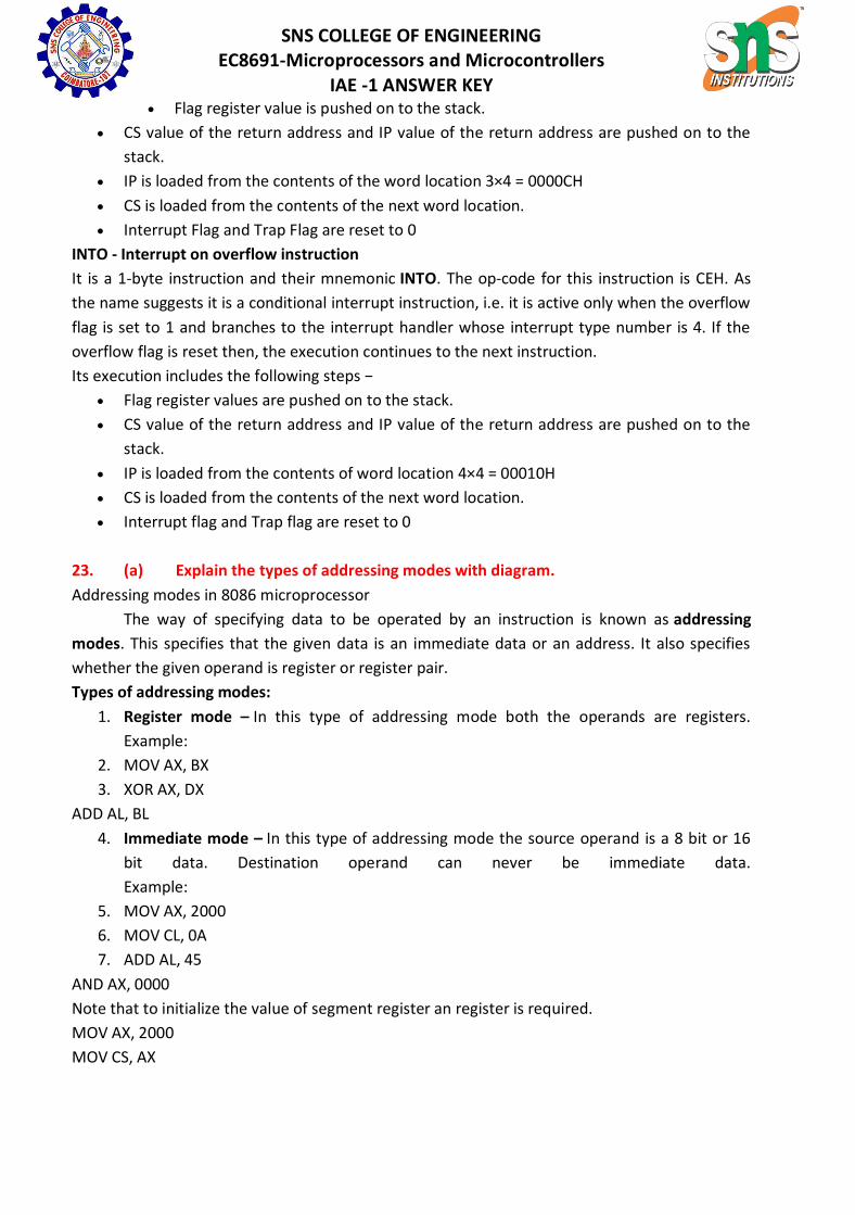
23. (a) Explain the types of addressing modes with diagram.
Addressing modes in 8086 microprocessor
The way of specifying data to be operated by an instruction is known as addressing
modes. This specifies that the given data is an immediate data or an address. It also specifies
whether the given operand is register or register pair.
Types of addressing modes:
1. Register mode – In this type of addressing mode both the operands are registers.
Example:
2. MOV AX, BX
3. XOR AX, DX
ADD AL, BL
4. Immediate mode – In this type of addressing mode the source operand is a 8 bit or 16
bit data. Destination operand can never be immediate data.
Example:
5. MOV AX, 2000
6. MOV CL, 0A
7. ADD AL, 45
AND AX, 0000
Note that to initialize the value of segment register an register is required.
MOV AX, 2000
MOV CS, AX

SNS COLLEGE OF ENGINEERING
EC8691-Microprocessors and Microcontrollers IAE -1 ANSWER KEY
8. Displacement or direct mode – In this type of addressing mode the effective
address is directly given in the instruction as displacement.
Example:
9. MOV AX, [DISP]
MOV AX, [0500]
10. Register indirect mode – In this addressing mode the effective address is in SI, DI or BX.
Example:
11. MOV AX, [DI]
12. ADD AL, [BX]
MOV AX, [SI]
13. Based indexed mode – In this the effective address is sum of base register and index
register.
14. Base register: BX, BP
Index register: SI, DI
The physical memory address is calculated according to the base register.
Example:
MOV AL, [BP+SI]
MOV AX, [BX+DI]
15. Indexed mode – In this type of addressing mode the effective address is sum of index
register and displacement.
Example:
16. MOV AX, [SI+2000]
MOV AL, [DI+3000]
17. Based mode – In this the effective address is the sum of base register and displacement.
Example:
MOV AL, [BP+ 0100]
18. Based indexed displacement mode – In this type of addressing mode the effective
address is the sum of index register, base register and displacement.
Example:
MOV AL, [SI+BP+2000]
19. String mode – This addressing mode is related to string instructions. In this the value of
SI and DI are auto incremented and decremented depending upon the value of

SNS COLLEGE OF ENGINEERING
EC8691-Microprocessors and Microcontrollers IAE -1 ANSWER KEY
directional flag.
Example:
20. MOVS B
MOVS W
21. Input/Output mode – This addressing mode is related with input output operations.
Example:
22. IN A, 45
OUT A, 50
23. Relative mode –In this the effective address is calculated with reference to instruction
pointer.
Example:
24. JNZ 8 bit address
IP=IP+8 bit address
(b) Explain stacks and procedures with neat diagram.
Stacks
The stack is a block of memory that may be used for temporarily storing the contents of
the registers inside the CPU. It is a top-down data structure whose elements are accessed using
the stack pointer (SP) which gets decremented by two as we store a data word into the stack
and gets incremented by two as we retrieve a data word from the stack back to the CPU
register.
The process of storing the data in the stack is called ‘pushing into’ the stack and the
reverse process of transferring the data back from the stack to the CPU register is known as
‘popping off’ the stack. The stack is essentially Last-In-First-Out (LIFO) data segment. This means
that the data which is pushed into the stack last will be on top of stack and will be popped off
the stack first.
The stack pointer is a 16-bit register that contains the offset address of the memory
location in the stack segment. The stack segment, like any other segment, may have a memory
block of a maximum of 64 Kbytes locations, and thus may overlap with any other segments.
Stack Segment register (SS) contains the base address of the stack segment in the memory.
The Stack Segment register (SS) and Stack pointer register (SP) together address the
stack-top as explained below:
If the stack top points to a memory location 52050H, it means that the location 52050H
is already occupied with the previously pushed data. The next 16 bit push operation will
decrement the stack pointer by two, so that it will point to the new stack-top 5204EH and the
decremented contents of SP will be 204EH. This location will now be occupied by the recently
pushed data.

SNS COLLEGE OF ENGINEERING
EC8691-Microprocessors and Microcontrollers IAE -1 ANSWER KEY
Thus for a selected value of SS, the maximum value of SP=FFFFH and the segment
can have maximum of 64K locations. If the SP starts with an initial value of FFFFH, it will be
decremented by two whenever a 16-bit data is pushed onto the stack. After successive push
operations, when the stack pointer contains 0000H, any attempt to further push the data to the
stack will result in stack overflow.
After a procedure is called using the CALL instruction, the IP is incremented to the next
instruction. Then the contents of IP, CS and flag register are pushed automatically to the stack.
The control is then transferred to the specified address in the CALL instruction i.e. starting
address of the procedure. Then the procedure is executed.
Procedures
A procedure is a set of code that can be branched to and returned from in such a way
that the code is as if it were inserted at the point from which it is branched to. The branch to
procedure is referred to as the call, and the corresponding branch back is known as the return.
The return is always made to the instruction immediately following the call regardless of where
the call is located.
1. Calls, Returns, and Procedure Definitions
The CALL instruction not only branches to the indicated address, but also pushes
the return address onto the stack. The RET instruction simply pops the return address from the
stack. The registers used by the procedure need to be stored before their contents are changed,
and then restored just before their contents are changed, and then restored just before the
procedure is excited.
A CALL may be direct or indirect and intrasegment or intersegment. If the CALL is intersegment,
the return must be intersegment. Intersegment call must push both (IP) and (CS) onto the stack.
The return must correspondingly pop two words from the stack. In the case of intrasegment call,
only the contents of IP will be saved and retrieved when call and return instructions are used.
Procedures are used in the source code by placing a statement of the form at the beginning of
the procedure. Procedure name PROC Attribute and by terminating the procedure with a
statement Procedure name ENDP.

SNS COLLEGE OF ENGINEERING
EC8691-Microprocessors and Microcontrollers IAE -1 ANSWER KEY
The attribute that can be used will be either NEAR or FAR. If the attribute is NEAR, the
RET instruction will only pop a word into the IP register, but if it is FAR, it will also pop a word
into the CS register.
A procedure may be in:
1. The same code segment as the statement that calls it.
2. A code segment that is different from the one containing the statement that calls it, but in
the same source module as the calling statement.
3. A different source module and segment from the calling statement.
In the first case, the attribute could be NEAR provided that all calls are in the same code
segment as the procedure. For the latter two cases the attribute must be FAR. If the procedure
is given a FAR attribute, then all calls to it must be intersegment calls even if the call is from the
same code segment. For the third case, the procedure name must be declared in EXTRN and
PUBLIC statements.
2. Saving and Restoring Registers
When both the calling program and procedure share the same set of registers, it is
necessary to save the registers when entering a procedure, and restore them before
returning to the calling program.
MSK PROC NEAR
PUSH AX
PUSH BX
PUSH CX
POP CX
POP BX
POP AX
RET
MSK ENDP
3. Procedure Communication
There are two general types of procedures, those operate on the same set of
data and those that may process a different set of data each time they are called. If a procedure
is in the same source module as the calling program, then the procedure can refer to the
variables directly.
When the procedure is in a separate source module it can still refer to the source module
directly provided that the calling program contains the directive
PUBLIC ARY, COUNT, SUM
EXTRN ARY: WORD, COUNT: WORD, SUM: WORD
4. Recursive Procedures
When a procedure is called within another procedure it called recursive
procedure. To make sure that the procedure does not modify itself, each call must store its set
of parameters, registers, and all temporary results in a different place in memory
Eg. Recursive procedure to compute the factorial

SNS COLLEGE OF ENGINEERING
EC8691-Microprocessors and Microcontrollers IAE -1 ANSWER KEY
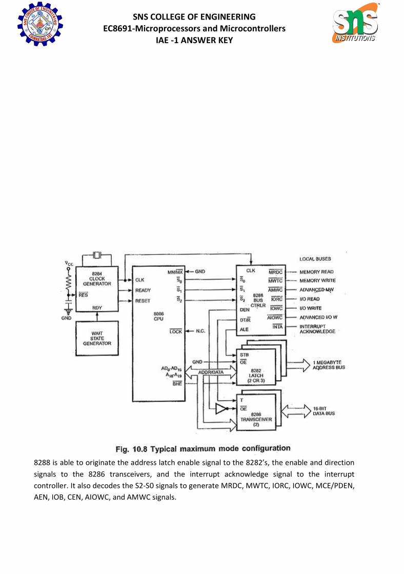
24. (a) Explain the maximum mode of 8086 with block diagram.
Maximum Mode Configuration of 8086: A processor is in the Maximum Mode
Configuration of 8086 when its MN/MX pin is grounded. The maximum mode defines pins 24 to
31 as follows:
Pin Definitions (24 to 31) in Maximum Mode:
1. QS1, QS0 (output) : These two output signals reflect the status of the instruction queue.
This status indicates the activity in the queue during the previous clock cycle.
2. S2,S1,S0 (output) : These three status signals indicate the type of transfer to be take place
during the current bus cycle.
3. LOCK: This signal indicates that an instruction with a LOCK prefix is being executed and the
bus is not to be used by another processor:
4. RQ/GT1 and RQ/GT0: In the Maximum Mode Configuration of 8086, HOLD and HLDA pins are
replaced by RQ (Bus request)/GT0 (Bus Grant), and RQ/GT1 signals. By using bus request signal
another master, can request for the system bus and processor communicate.that the request is
granted to the requesting master by using bus grantnal. Both signals are similar except the
RQ/GT0 has higher priority than RQ/GT1.
Maximum Mode Configuration:
Fig. 10.8 shows the typical Maximum Mode Configuration of 8086. In the maximum
mode additional circuitry is required to translate the control signals. The additional circuitry
converts the status signals (S2-S0) into the I/O and memory transfer signals. It also generates
the control signals required to direct the data flow and for controlling 8282 latches and 8286
transceivers. The Intel 8288 bus controller is used to implement this control circuitry.
SNS COLLEGE OF ENGINEERING
EC8691-Microprocessors and Microcontrollers IAE -1 ANSWER KEY
8288 is able to originate the address latch enable signal to the 8282’s, the enable and direction
signals to the 8286 transceivers, and the interrupt acknowledge signal to the interrupt
controller. It also decodes the S2-S0 signals to generate MRDC, MWTC, IORC, IOWC, MCE/PDEN,
AEN, IOB, CEN, AIOWC, and AMWC signals.

SNS COLLEGE OF ENGINEERING
EC8691-Microprocessors and Microcontrollers IAE -1 ANSWER KEY
MRDC (Memory Read Command) : It instructs the memory to put the contents of the
addressed location on the data bus.
MWTC (Memory Write Command) : It instructs the memory to accept the data on the data bus
and load the data into the addressed memory location.
IORC (I/O Read Command) : It instructs an I/O device to put the data contained in the
addressed port on the data bus.
IOWC (I/0 Write Command) : It instructs an I/O device to accept the data on the data bus and
load the data into the addressed port.
MCE/PDEN (Master Cascade Enable/Peripheral Data Enable) : It controls the mode of
operation of 8259. It selects cascade operation for 8259 (interrupt controller) if IOB signal is
grounded and enables the I/O bus transceivers if IOB is tied high.
AEN, IOB and CEN : These pins are used in multiprocessor system. With a single processor in
the system, AEN and IOB are grounded and CEN is tied high. AEN causes the 8288 to enable the
memory control signals. IOB (I/O bus mode) signal selects either the I/O bus mode or system
bus mode operation. CEN (control enable) input enables the command output pins on the 8288.
AIOWC/AMWC (Advance I/O Write Command/Advance Memory Write Command) : These
signals are similar to IOWC and MWTC except that they are activated one clock pulse earlier.
This gives slow interfaces an extra clock cycle to prepare to input the data.
(b) Draw and explain the pin diagram of minimum mode of operation.
Pin Diagram and Pin description of 8086

SNS COLLEGE OF ENGINEERING
EC8691-Microprocessors and Microcontrollers IAE -1 ANSWER KEY
The following pin function descriptions are for the microprocessor 8086 in either minimum or
maximum mode.
AD0 - AD15 (I/O): Address Data Bus
These lines constitute the time multiplexed memory/IO address during the first clock cycle (T1)
and data during T2, T3 and T4 clock cycles. A0 is analogous to BHE for the lower byte of the data
bus, pins D0-D7. A0 bit is Low during T1 state when a byte is to be transferred on the lower
portion of the bus in memory or I/O operations. 8-bit oriented devices tied to the lower half
would normally use A0 to condition chip select functions. These lines are active high and float to
tri-state during interrupt acknowledge and local bus "Hold acknowledge".
A19/S6, A18/S5, A17/S4, A16/S3 (0): Address/Status
During T1 state these lines are the four most significant address lines for memory operations.
During I/O operations these lines are low. During memory and I/O operations, status
information is available on these lines during T2, T3, and T4 states.S5: The status of the interrupt
enable flag bit is updated at the beginning of each cycle. The status of the flag is indicated
through this bus.
S6:
When Low, it indicates that 8086 is in control of the bus. During a "Hold acknowledge" clock
period, the 8086 tri-states the S6 pin and thus allows another bus master to take control of the
status bus.
S3 & S4:
Lines are decoded as follows:
A17/S4 A16/S3 Function

SNS COLLEGE OF ENGINEERING
EC8691-Microprocessors and Microcontrollers IAE -1 ANSWER KEY
0 0 Extra segment access
0 1 Stack segment access
1 0 Code segment access
1 1 Data segment access
After the first clock cycle of an instruction execution, the A17/S4 and A16/S3 pins specify which
segment register generates the segment portion of the 8086 address. Thus by decoding these
lines and using the decoder outputs as chip selects for memory chips, up to 4 Megabytes (one
Mega per segment) of memory can be accesses. This feature also provides a degree of
protection by preventing write operations to one segment from erroneously overlapping into
another segment and destroying information in that segment.
BHE /S7 (O): Bus High Enable/Status
During T1 state theBHE should be used to enable data onto the most significant half of the data
bus, pins D15 - D8. Eight-bit oriented devices tied to the upper half of the bus would normally
use BHE to control chip select functions. BHE is Low during T1 state of read, write and interrupt
acknowledge cycles when a byte is to be transferred on the high portion of the bus.
The S7 status information is available during T2, T3 and T4 states. The signal is active Low and
floats to 3-state during "hold" state. This pin is Low during T1 state for the first interrupt
acknowledge cycle.
RD (O): READ
The Read strobe indicates that the processor is performing a memory or I/O read cycle. This
signal is active low during T2 and T3 states and the Tw states of any read cycle. This signal floats
to tri-state in "hold acknowledge cycle".
TEST (I)
TEST pin is examined by the "WAIT" instruction. If the TEST pin is Low, execution continues.
Otherwise the processor waits in an "idle" state. This input is synchronized internally during
each clock cycle on the leading edge of CLK.
INTR (I): Interrupt Request
It is a level triggered input which is sampled during the last clock cycle of each instruction to
determine if the processor should enter into an interrupt acknowledge operation. A subroutine
is vectored to via an interrupt vector look up table located in system memory. It can be
internally masked by software resetting the interrupt enable bit INTR is internally synchronized.
This signal is active HIGH.
NMI (I): Non-Maskable Interrupt
An edge triggered input, causes a type-2 interrupt. A subroutine is vectored to via the interrupt
vector look up table located in system memory. NMI is not maskable internally by software. A

SNS COLLEGE OF ENGINEERING
EC8691-Microprocessors and Microcontrollers IAE -1 ANSWER KEY
transition from a LOW to HIGH on this pin initiates the interrupt at the end of the current
instruction. This input is internally synchronized.
Reset (I)
Reset causes the processor to immediately terminate its present activity. To be recognised, the
signal must be active high for at least four clock cycles, except after power-on which requires a
50 Micro Sec. pulse. It causes the 8086 to initialize registers DS, SS, ES, IP and flags to all zeros. It
also initializes CS to FFFF H. Upon removal of the RESET signal from the RESET pin, the 8086 will
fetch its next instruction from the 20 bit physical address FFFF0H. The reset signal to 8086 can
be generated by the 8284. (Clock generation chip). To guarantee reset from power-up, the reset
input must remain below 1.5 volts for 50 Micro sec. after Vcc has reached the minimum supply
voltage of 4.5V.
Ready (I)
Ready is the acknowledgement from the addressed memory or I/O device that it will complete
the data transfer. The READY signal from memory or I/O is synchronized by the 8284 clock
generator to form READY. This signal is active HIGH. The 8086 READY input is not synchronized.
Correct operation is not guaranteed if the setup and hold times are not met.
CLK (I): Clock
Clock provides the basic timing for the processor and bus controller. It is asymmetric with 33%
duty cycle to provide optimized internal timing. Minimum frequency of 2 MHz is required, since
the design of 8086 processors incorporates dynamic cells. The maximum clock frequencies of
the 8086-4, 8086 and 8086-2 are4MHz, 5MHz and 8MHz respectively. Since the 8086 does not
have on-chip clock generation circuitry, and 8284 clock generator chip must be connected to the
8086 clock pin. The crystal connected to 8284 must have a frequency 3 times the 8086 internal
frequency. The 8284 clock generation chip is used to generate READY, RESET and CLK.
MN/MX (I): Maximum / Minimum
This pin indicates what mode the processor is to operate in. In minimum mode, the 8086 itself
generates all bus control signals. In maximum mode the three status signals are to be decoded
to generate all the bus control signals. Minimum Mode Pins The following 8 pins function
descriptions are for the 8086 in minimum mode; MN/ MX = 1. The corresponding 8 pins function
descriptions for maximum mode is explained later.
M/IO (O): Status line
This pin is used to distinguish a memory access or an I/O accesses. When this pin is Low, it
accesses I/O and when high it access memory. M / IO becomes valid in the T4 state preceding a
bus cycle and remains valid until the final T4 of the cycle. M/IO floats to 3 - state OFF during
local bus "hold acknowledge".
WR (O): Write
Indicates that the processor is performing a write memory or write IO cycle, depending on the
state of the M /IOsignal. WR is active for T2, T3 and Tw of any write cycle. It is active LOW, and
floats to 3-state OFF during local bus "hold acknowledge ".
INTA (O): Interrupt Acknowledge
SNS COLLEGE OF ENGINEERING
EC8691-Microprocessors and Microcontrollers IAE -1 ANSWER KEY
It is used as a read strobe for interrupt acknowledge cycles. It is active LOW during T2,
T3, and T4 of each interrupt acknowledge cycle.
ALE (O): Address Latch Enable
ALE is provided by the processor to latch the address into the 8282/8283 address latch. It is an
active high pulse during T1 of any bus cycle. ALE signal is never floated.
DT/ R (O): DATA Transmit/Receive
In minimum mode, 8286/8287 transceiver is used for the data bus. DT/ R is used to control the
direction of data flow through the transceiver. This signal floats to tri-state off during local bus
"hold acknowledge".
DEN (O): Data Enable
It is provided as an output enable for the 8286/8287 in a minimum system which uses the
transceiver. DEN is active LOW during each memory and IO access. It will be low beginning with
T2 until the middle of T4, while for a write cycle, it is active from the beginning of T2 until the
middle of T4. It floats to tri-state off during local bus "hold acknowledge".
HOLD & HLDA (I/O): Hold and Hold Acknowledge
Hold indicates that another master is requesting a local bus "HOLD". To be acknowledged, HOLD
must be active HIGH. The processor receiving the "HOLD " request will issue HLDA (HIGH) as an
acknowledgement in the middle of the T1-clock cycle. Simultaneous with the issue of HLDA, the
processor will float the local bus and control lines. After "HOLD" is detected as being Low, the
processor will lower the HLDA and when the processor needs to run another cycle, it will again
drive the local bus and control lines. Maximum Mode The following pins function descriptions
are for the 8086/8088 systems in maximum mode (i.e.. MN/MX = 0). Only the pins which are
unique to maximum mode are described below.
S2, S1, S0 (O): Status Pins
These pins are active during T4, T1 and T2 states and is returned to passive state (1,1,1 during
T3 or Tw (when ready is inactive). These are used by the 8288 bus controller to generate all
memory and I/O operation) access control signals. Any change by S2, S1, S0 during T4 is used to
indicate the beginning of a bus cycle. These status lines are encoded as shown in table 3.
S2 S1 S0 Characteristics
0 0 0 Interrupt acknowledge
0 0 1 Read I/O port
0 1 0 Write I/O port
0 1 1 Halt
1 0 0 Code access1 0 1 Read memory

SNS COLLEGE OF ENGINEERING
EC8691-Microprocessors and Microcontrollers IAE -1 ANSWER KEY
1 1 0 Write memory
1 1 1 Passive State
QS0, QS1 (O): Queue – Status
Queue Status is valid during the clock cycle after which the queue operation is performed. QS0,
QS1 provide status to allow external tracking of the internal 8086 instruction queue. The
condition of queue status is shown in table 4.
Queue status allows external devices like In-circuit Emulators or special instruction set extension
co-processors to track the CPU instruction execution. Since instructions are executed from the
8086 internal queue, the queue status is presented each CPU clock cycle and is not related to
the bus cycle activity. This mechanism allows (1) A processor to detect execution of a ESCAPE
instruction which directs the co- processor to perform a specific task and (2) An in-circuit
Emulator to trap execution of a specific memory location.
QS1 QS1 Characteristics
0 0 No operation
0 1 First byte of opcode from queue
1 0 Empty the queue
1 1 Subsequent byte from queue
LOCK (O)
It indicates to another system bus master, not to gain control of the system bus while LOCK is
active Low. The LOCK signal is activated by the "LOCK" prefix instruction and remains active until
the completion of the instruction. This signal is active Low and floats to tri-state OFF during
'hold acknowledge'. Example:
LOCK XCHG reg., Memory ; Register is any register and memory GT0
; is the address of the semaphore.
RQ/GT0 and RQ/GT1 (I/O): Request/Grant
These pins are used by other processors in a multi processor organization. Local bus masters of
other processors force the processor to release the local bus at the end of the processors
current bus cycle. Each pin is bi-directional and has an internal pull up resistors. Hence they may
be left un-connected.
25. (a) Explain the coprocessor and closely coupled configuration.
Coprocessor configurations

SNS COLLEGE OF ENGINEERING
EC8691-Microprocessors and Microcontrollers IAE -1 ANSWER KEY
WAIT instruction allows the processor to synchronize itself with external hardware, eg.,
waiting for 8087 math co-processor.
When the CPU executes WAIT waiting state.
TEST input is asserted (low), the waiting state is completed and execution will resume. ESC
instruction:
ESC opcode, operand, opcode: immediate value recognizable to a coprocessor as an instruction
opcode
Operand: name of a register or a memory address (in any mode)
When the CPU executes the ESC instruction, the processor accesses the memory
operand by placing the address on the address bus.
If a coprocessor is configured to share the system bus, it will recognize the ESC instruction and
therefore will get the opcode and the operand

SNS COLLEGE OF ENGINEERING
EC8691-Microprocessors and Microcontrollers IAE -1 ANSWER KEY
Coprocessor cannot take control of the bus, it does everything through the CPU
Closely Coupled processor may take control of the bus independently - 8089 shares
CPU’s clock and bus control logic.
Communication with host CPU is by way of shared memory
Host sets up a message (command) in memory
Independent processor interrupts host on completion
Two 8086’s cannot be closely coupled

SNS COLLEGE OF ENGINEERING
EC8691-Microprocessors and Microcontrollers IAE -1 ANSWER KEY
Closely Coupled Configuration

SNS COLLEGE OF ENGINEERING
EC8691-Microprocessors and Microcontrollers IAE -1 ANSWER KEY
(b) Explain the types of system bus timing.
Types:
1. Minimum mode 8086 system bus timings
2. Maximum mode 8086 system bus timings
System Bus timings: Minimum mode 8086 system bus timings
In a minimum mode 8086 system, the microprocessor 8086 is operated in minimum
mode by strapping its MN/MX* pin to logic1. In this mode, all the control signals are given out
by the microprocessor chip itself. There is a single microprocessor in the minimum mode
system. The remaining components in the system are latches, transreceivers, clock generator,
memory and I/O devices.
The opcode fetch and read cycles are similar. Hence the timing diagram can be
categorized in two parts, the first is the timing diagram for read cycle and the second is the
timing diagram for write cycle. The read cycle begins in T1 with the assertion of the address
latch enable (ALE) signal and also M/IO* signal. During the negative going edge of this signal, the
valid address is latched on the local bus. The BHE* and A0 signals address low, high or both
bytes. From Tl to T4, the M/IO* signal indicates a memory or I/O operation. At T2 the address is
removed from the local bus and is sent to the output. The bus is then tristated. The read (RD*)
control signal is also activated in T2 .The read (RD) signal causes the addressed device to enable
its data bus drivers. After RD* goes low, the valid data is available on the data bus. The

SNS COLLEGE OF ENGINEERING
EC8691-Microprocessors and Microcontrollers IAE -1 ANSWER KEY
addressed device will drive the READY line high, when the processor returns the read signal to
high level, the addressed device will again tristate its bus drivers.
A write cycle also begins with the assertion of ALE and the emission of the address. The M/IO*
signal is again asserted to indicate a memory or I/O operation. In T2 after sending the address in
Tl the processor sends the data to be written to the addressed location. The data remains on the
bus until middle of T4 state. The WR* becomes active at the beginning ofT2 (unlike RD* is
somewhat delayed in T2 to provide time for floating). The BHE* and A0 signals are used to select
the proper byte or bytes of memory or I/O word to be read or written. The M/IO*, RD* and
WR* signals indicate the types of data transfer as specified in Table
Table 2.5 Read write cycle

SNS COLLEGE OF ENGINEERING
EC8691-Microprocessors and Microcontrollers IAE -1 ANSWER KEY