sn65hvda100-q1 lin physical interface
TRANSCRIPT

VSUP
INH
LIN
GND
NWAKE
1
2
3
4
8
7
6
5
RXD
EN
TXD
Receiver
VSUP/2
Wake up
State
INH Control
Fault Detection
and Protection
Dominant State
Timeout
Filter
Driver with
Slope Control
Filter30lQ
VSUP
Product
Folder
Sample &Buy
Technical
Documents
Tools &
Software
Support &Community
SN65HVDA100-Q1SLIS128C –NOVEMBER 2011–REVISED JULY 2015
SN65HVDA100-Q1 LIN Physical Interface1 Features 3 Description
The SN65HVDA100 device is the Local Interconnect1• Qualified for Automotive Applications
Network (LIN) physical interface, which integrates the• Local Interconnect Network (LIN) Physical Layer serial transceiver with wakeup and protectionSpecification Revision 2.1 Compliant and features. The LIN bus is a single-wire bidirectionalConforms to SAEJ2602 Recommended Practice bus typically used for low-speed in-vehicle networksfor LIN using data rates from 2.4 kbps to 20 kbps. The LIN
protocol output data stream on TXD is converted by• Extended Operation With Supply From 5 V tothe SN65HVDA100 into the LIN bus signal through a27 V DC (LIN Specification 7 V to 18 V)current-limited wave-shaping driver as outlined by the• LIN Transmit Speed up to 20-kbps LIN Specified LIN Physical Layer Specification. The receiverMaximum, High-Speed Receive Capable converts the data stream from the LIN bus and
• Sleep Mode: Ultra-Low Current Consumption outputs the data stream through RXD. The LIN busAllows Wake-Up Events From: LIN Bus, Wake-Up has two states: dominant state (voltage near ground)
and recessive state (voltage near battery). In theInput (External Switch) or Host MCUrecessive state, the LIN bus is pulled high by the• Wake-Up Request on RXD Pininternal pullup resistor (30 kΩ) and series diode, so
• Wake-Up Source Recognition on TXD Pin no external pullup components are required for slave• Interfaces to MCU With 5-V or 3.3-V I/O Pins applications. Master applications require an external
pullup resistor (1 kΩ) plus a series diode per the LIN• High Electromagnetic Compatibility (EMC)specification.• Control of External Voltage Regulator (INH Pin)
• Supports ISO9141 (K-Line) -Like Functions Device Information(1)
• ESD Protection to ±12 kV (Human Body Model) PART NUMBER PACKAGE BODY SIZE (NOM)on LIN Pin SN65HVDA100-Q1 SOIC (8) 4.90 mm × 3.91 mm
• LIN Pin Handles Voltage From –27 V to 45 V (1) For all available packages, see the orderable addendum at(Short to Battery or Ground) the end of the data sheet.
• Survives Transient Damage in AutomotiveSN65HVDA100-Q1 Block DiagramEnvironment (ISO 7637)
• Undervoltage Protection on VSUP
• TXD Dominant State Time-Out Protection• Prevention of False Wakeups With Bus Stuck
Dominant Fault• Thermal Shutdown• Unpowered Node or Ground Disconnection
Failsafe at System Level, Node Does Not DisturbBus (No Load on Bus)
2 Applications• Automotive• Industrial Sensing• White Goods Distributed Control
1
An IMPORTANT NOTICE at the end of this data sheet addresses availability, warranty, changes, use in safety-critical applications,intellectual property matters and other important disclaimers. PRODUCTION DATA.

SN65HVDA100-Q1SLIS128C –NOVEMBER 2011–REVISED JULY 2015 www.ti.com
Table of Contents9.1 Overview ................................................................. 121 Features .................................................................. 19.2 Functional Block Diagram ....................................... 122 Applications ........................................................... 19.3 Feature Description................................................. 123 Description ............................................................. 19.4 Device Functional Modes........................................ 164 Revision History..................................................... 2
10 Application and Implementation........................ 185 Description (continued)......................................... 310.1 Application Information.......................................... 186 Pin Configuration and Functions ......................... 310.2 Typical Application ............................................... 187 Specifications......................................................... 4 11 Power Supply Recommendations ..................... 217.1 Absolute Maximum Ratings ..................................... 4
12 Layout................................................................... 217.2 ESD Ratings.............................................................. 412.1 Layout Guidelines ................................................. 217.3 Recommended Operating Conditions....................... 412.2 Layout Example .................................................... 227.4 Thermal Information .................................................. 4
13 Device and Documentation Support ................. 237.5 Electrical Characteristics........................................... 513.1 Community Resources.......................................... 237.6 Switching Characteristics .......................................... 713.2 Trademarks ........................................................... 237.7 Dissipation Ratings ................................................... 813.3 Electrostatic Discharge Caution............................ 237.8 Typical Characteristics ............................................ 1113.4 Glossary ................................................................ 238 Parameter Measurement Information ................ 11
14 Mechanical, Packaging, and Orderable9 Detailed Description ............................................ 12 Information ........................................................... 23
4 Revision HistoryNOTE: Page numbers for previous revisions may differ from page numbers in the current version.
Changes from Revision B (January 2014) to Revision C Page
• Added Pin Configuration and Functions section, ESD Ratings table, Feature Description section, Device FunctionalModes, Application and Implementation section, Power Supply Recommendations section, Layout section, Deviceand Documentation Support section, and Mechanical, Packaging, and Orderable Information section .............................. 1
Changes from Revision A (January 2013) to Revision B Page
• Ordered PIN ASSIGNMENTS table alphabetically by pin name............................................................................................ 3• Added new Mode Transitions section, including a new figure ............................................................................................. 18• Revised the application schematic diagram ......................................................................................................................... 19
Changes from Original (November 2011) to Revision A Page
• Deleted -03V to 45V from the 1.5 row in the abs max table, units column............................................................................ 4• Changed added Delta and corrected Hysteresis in elec chara table, row 4.4 and changed the TYP column from 4.5
to 0.2....................................................................................................................................................................................... 5• Deleted rows 9.1 and 9.2 from the elec chara table............................................................................................................... 6• Added Minimum to the statement in parens in front of dominant, row 11.9 of elec chara table ............................................ 7
2 Submit Documentation Feedback Copyright © 2011–2015, Texas Instruments Incorporated
Product Folder Links: SN65HVDA100-Q1

1
2
3
4
8
7
6
5
RXD
EN
NWake
TXD
INH
VSUP
LIN
GND
SN65HVDA100-Q1www.ti.com SLIS128C –NOVEMBER 2011–REVISED JULY 2015
5 Description (continued)In sleep mode, low quiescent current is needed even though the wake-up circuits remain active and allow forremote wake up through the LIN bus or local wake up through the NWake or EN pins.
The SN65HVDA100 has been designed for operation in the harsh automotive environment. The device alsoprevents back-feed current through LIN to the supply input in case of a ground shift or supply voltagedisconnection. The device also features undervoltage, overtemperature, and loss-of-ground protection. In theevent of a fault condition, the transmitter is immediately switched off and remains off until the fault condition isremoved.
6 Pin Configuration and Functions
D Package8-Pin SOICTop View
Pin FunctionsPIN
TYPE DESCRIPTIONNAME NO.
EN 2 I Enable inputGND 5 GND GroundINH 8 O Inhibit controls external voltage regulator with inhibit inputLIN 6 I/O LIN bus single-wire transmitter and receiverNWake 3 I High-voltage input for device wake upRXD 1 O RXD output (open-drain) interface reporting state of LIN bus voltageTXD 4 I TXD input interface to control state of LIN outputVSUP 7 Supply Device supply voltage (connected to battery in series with external reverse blocking diode)
Copyright © 2011–2015, Texas Instruments Incorporated Submit Documentation Feedback 3
Product Folder Links: SN65HVDA100-Q1

SN65HVDA100-Q1SLIS128C –NOVEMBER 2011–REVISED JULY 2015 www.ti.com
7 Specifications
7.1 Absolute Maximum Ratings (1) (2)
MIN MAX UNITVSUP Supply line supply voltage (LIN 2.1 Param 11) –0.3 45 VVLIN LIN input voltage –27 45 VVNWAK NWake input voltage (through serial resistor ≥ 2 kΩ ) –0.3 45 VE
IO Output current –50 2 mAVINH INH voltage –0.3 Vsup + 0.3 VVLogic Logic pin voltage RXD, TXD, EN –0.3 5.5 VTA Operational free-air (ambient) temperature –40 125 °CTJ Junction temperature –40 150 °CTLEAD Lead temperature (soldering, 10 seconds) 260 °CTstg Storage temperature –65 150 °C
(1) Stresses beyond those listed under Absolute Maximum Ratings may cause permanent damage to the device. These are stress ratingsonly, which do not imply functional operation of the device at these or any other conditions beyond those indicated under RecommendedOperating Conditions. Exposure to absolute-maximum-rated conditions for extended periods may affect device reliability.
(2) All voltage values are with respect to GND.
7.2 ESD RatingsVALUE UNIT
All pins ±4000Human body model (HBM), per AEC LIN bus pin (2) ±12000Q100-002 (1)V(ESD) Electrostatic discharge V
NWake pin (3) ±11000Charged device model (CDM), per AEC Q100-011 ±1500
(1) AEC Q100-002 indicates that HBM stressing shall be in accordance with the ANSI/ESDA/JEDEC JS-001 specification.(2) Test method based upon AEC-Q100-002, LIN bus pin stressed with respect to GND.(3) Test method based upon AEC-Q100-002, NWake pin stressed with respect to GND.
7.3 Recommended Operating ConditionsMIN MAX UNIT
VSUP Supply line supply voltage (LIN 2.1 Param 10) 5 27 VVLIN LIN input voltage 0 18 VVNWake NWake input voltage 0 27 VVINH INH voltage 0 27 VVLogic Logic voltage 0 5.25 VTA Operational free-air temperature (see Thermal Information) –40 125 °C
7.4 Thermal InformationSN65HVDA100-Q1
THERMAL METRIC (1) D (SOIC) UNIT8 PINS
RθJA Junction-to-ambient thermal resistance 112.5 °C/WRθJC(top) Junction-to-case (top) thermal resistance 66.3 °C/WRθJB Junction-to-board thermal resistance 52.9 °C/WψJT Junction-to-top characterization parameter 19.3 °C/WψJB Junction-to-board characterization parameter 52.4 °C/W
(1) For more information about traditional and new thermal metrics, see the Semiconductor and IC Package Thermal Metrics applicationreport, SPRA953.
4 Submit Documentation Feedback Copyright © 2011–2015, Texas Instruments Incorporated
Product Folder Links: SN65HVDA100-Q1

SN65HVDA100-Q1www.ti.com SLIS128C –NOVEMBER 2011–REVISED JULY 2015
7.5 Electrical CharacteristicsVSUP = 5V to 27 V, TJ = –40°C to 150°C (unless otherwise noted)
PARAMETER TEST CONDITIONS MIN TYP (1) MAX UNITVSUP SUPPLY
Operational supply Device is operational beyond the LIN definedVSUP voltage (LIN 2.1 nominal supply line voltage range of 5 V < 5 14 27 V
Param 10) (2) VSUP < 27 VNominal supply Normal and standby modes 7 14 18
VSUP voltage (LIN 2.1 VSleep mode 7 12 18Param 10)
UVSUP Undervoltage VSUP threshold 4.35 4.65 VUVHYS Delta hysteresis voltage for VSUP undervoltage threshold 0.2 V
Normal mode, EN = high, Bus dominant(total bus load where RLIN ≥ 500 Ω and 1.2 7.5 mACLIN ≤ 10 nF (see Figure 9) (3), INH = VSUP,NWake = VSUP
Standby mode, EN = low, Bus dominant(total bus load where RLIN ≥ 500 Ω and 1 2.1 mACLIN ≤ 10 nF (see Figure 9) (3), INH = VSUP,NWake = VSUP
Normal mode, EN = high, Bus recessive, 450 775 μAISUP Supply current LIN = VSUP, INH = VSUP, NWake = VSUP
Standby mode, EN = low, Bus recessive, 450 775 μALIN = VSUP, INH = VSUP, NWake = VSUP
Sleep mode, 7 V < VSUP ≤ 14 V,LIN = VSUP, NWake = VSUP, EN = 0 V, TXD 10 20 μAand RXD floatingSleep mode, 14 V < VSUP < 27 V,LIN = VSUP, NWake = VSUP, EN = 0 V, TXD 30 μAand RXD floating
RXD OUTPUT PIN (OPEN DRAIN)VO Output voltage (4) –0.3 5.5 V
Low-level outputIOL LIN = 0 V, RXD = 0.4 V 3.5 mAcurrent, open drainLeakage current, high-IIKG LIN = VSUP, RXD = 5 V –5 0 5 μAlevel
TXD INPUT/OUTPUT PINVIL Low-level input voltage –0.3 0.8 VVIH High-level input voltage 2 5.5 VVIT Input threshold hysteresis voltage 30 500 mV
Pulldown resistor 125 350 800 kΩLow-level input TXD = LowIIL –5 0 5 μAleakage currentLocal wake up source Standby mode after a local wake up event,
ITXD_Wake re recognition TXD VLIN = VSUP, NWake = 0 V, 1.3 4.6 8 mAopen drain drive TXD = 1 V
LIN PIN (REFERENCED TO VSUP)High-level output LIN recessive, TXD = high, IO = 0 mA,VOH VSUP – 1 Vvoltage VSUP = 14 VLow-level output LIN dominant, TXD = low, IO = 40 mA,VOL 0.2 × VSUP Vvoltage VSUP = 14 V
(1) Typical values are given for VSUP = 14 V at 25°C, except for low power mode where typical values are given for VSUP = 12 V at 25°C.(2) All voltages are defined with respect to ground; positive currents flow into the SN65HVDA100 device.(3) In the dominant state, the supply current increases as the supply voltage increases due to the integrated LIN slave termination
resistance. At higher voltages the majority of supply current is through the termination resistance. The minimum resistance of the LINslave termination is 20 kΩ, so the maximum supply current attributed to the termination is:ISUP (dom) max termination ≉ (VSUP –(VLIN_Dominant + 0.7 V) / 20 kΩ.
(4) RXD pin output is open drain. Output voltage is through external pullup resistance to logic supply of the system and impedance of theRXD pin.
Copyright © 2011–2015, Texas Instruments Incorporated Submit Documentation Feedback 5
Product Folder Links: SN65HVDA100-Q1
SN65HVDA100-Q1SLIS128C –NOVEMBER 2011–REVISED JULY 2015 www.ti.com
Electrical Characteristics (continued)VSUP = 5V to 27 V, TJ = –40°C to 150°C (unless otherwise noted)
PARAMETER TEST CONDITIONS MIN TYP (1) MAX UNITLimiting current (LINIL TXD = 0 V, VLIN = 7 V to 27 V 40 90 200 mA2.1 Param 12)Receiver leakagecurrent, dominant (LIN LIN = 0 V, 7 V ≤VSUP ≤ 18 V, Driver off –1 mA2.1 Param 13)
ILKG Receiver leakage LIN ≥ VSUP, 7 ≤ VSUP ≤18 V, Driver off 20current, recessive μA
LIN = VSUP, driver off –5 5(LIN 2.1 Param 14)Leakage current, loss GND = VSUP , VSUP = 12 V,ILKG of ground (LIN 2.1 –1 1 mA0 V < VLIN < 18 VParam 15)Leakage current, loss 7 V < LIN ≤ 12 V, VSUP = GND 5
ILKG of supply (LIN 2.1 μA12 V < LIN ≤ 18 V, VSUP = GND 10Param 16)
Low-level input LIN dominant (including LIN dominant forVIL voltage (LIN 2.1 0.4 × VSUP Vwake up)Param 17)High-level input
VIH voltage (LIN 2.1 LIN recessive 0.6 × VSUP VParam 18)Receiver center
VBUS_CNT threshold (LIN 2.1 VBUS_CNT = (VIL + VIH) / 2 0.475 x VSUP 0.5 × VSUP 0.525 x VSUP VParam 19)Hysteresis voltageVHYS VHYS = (VIL - VIH) 0.05 × VSUP 0.175 × VSUP V(LIN 2.1 Param 20)Serial diode in LIN
VSERIAL_ termination pull up By design and characterization 0.4 0.7 1.0 VDIODE path (LIN 2.1 Param
21)Pullup resistor to VSUPRSLAVE Normal and standby modes 20 30 60 kΩ(LIN 2.1 Param 26)Pullup current sourceRSLEEP Sleep mode, VSUP = 14 V, LIN = GND –2 –20 μAto VSUP
EN INPUT PINLow-level inputVIL –0.3 0.8 VvoltageHigh-level inputVIH 2 5.5 Vvoltage
Vhys Hysteresis voltage By design and characterization 30 500 mVPulldown resistor 125 350 800 kΩLow-level inputIIL EN = Low –5 0 5 μAcurrent
INH OUTPUT PINBetween VSUP and INH, INH = 2-mA drive,RDS(on) ON-state resistance 25 50 ΩNormal or standby mode
IIKG Leakage current Low-power mode, 0 < INH < VSUP –5 0 5 μA
6 Submit Documentation Feedback Copyright © 2011–2015, Texas Instruments Incorporated
Product Folder Links: SN65HVDA100-Q1

SN65HVDA100-Q1www.ti.com SLIS128C –NOVEMBER 2011–REVISED JULY 2015
Electrical Characteristics (continued)VSUP = 5V to 27 V, TJ = –40°C to 150°C (unless otherwise noted)
PARAMETER TEST CONDITIONS MIN TYP (1) MAX UNITNWAKE INPUT PIN
Low-level inputVIL –0.3 VSUP – 3.3 VvoltageHigh-level inputVIH VSUP – 1 VSUP + 0.3 VvoltagePullup current NWake = 0 V –45 –10 –2 μA
IIKG Leakage current VSUP = NWake –5 0 5 μAAC CHARACTERISTICS
THREC(max) = 0.744 × VSUP,Duty cycle 1 (5) (LIN THDOM(maximum) = 0.581 × VSUP,D1 0.3962.1 Param 27) VSUP = 7 V to 18 V, tBIT = 50 μs (20 kbps),
D1 = tBus_rec(min)/ (2 × tBIT) (see Figure 1)THREC(min) = 0.422 × VSUP,THDOM(min) = 0.284 × VSUP,Duty cycle 2 (5) (LIND2 VSUP = 7.6 V to 18 V, 0.5812.1 Param 28) tBIT = 50 μs (20 kbps),D2 = tBus_rec(max)/ (2 × tBIT) (see Figure 1)THREC(max) = 0.778 × VSUP,THDOM(max) = 0.616 × VSUP,Duty cycle 3 (5) (LIND3 VSUP = 7 V to 18 V, 0.4172.1 Param 29) tBIT = 96 μs (10.4 kbps),D3 = tBus_rec(min)/ (2 × tBIT) (see Figure 1)THREC(min) = 0.389 × VSUP,THDOM(min) = 0.251 × VSUP,Duty cycle 4 (5) (LIND4 VSUP = 7.6 V to 18 V, 0.592.1 Param 30) tBIT = 96 μs (10.4 kbps),D4 = tBus_rec(max)/ (2 × tBIT) (see Figure 1)
(5) Duty cycles: LIN driver bus load conditions (CLINBUS, RLINBUS): Load1 = 1 nF, 1 kΩ; Load2 = 10 nF, 500 Ω. Duty cycles 3 and 4 aredefined for 10.4-kbps operation. The SN65HVDA100 also meets these lower data rate requirements, while it is capable of the higherspeed 20-kbps operation as specified by duty cycles 1 and 2. SAEJ2602 derives propagation delay equations from the LIN 2.0 dutycycle definitions, for details see the SAEJ2602 specification.
7.6 Switching Characteristicsover operating free-air temperature range (unless otherwise noted)
PARAMETER TEST CONDITIONS MIN TYP MAX UNITAC CHARACTERISTICS
Receiver rising propagation delay RRXD = 2.4 kΩ, CRXD = 20 pFtrx_pdr 6 μstime (LIN 2.1 Param 31) (see Figure 2 and Figure 9)Receiver falling propagation delay RRXD = 2.4 kΩ, CRXD = 20 pFtrx_pdf 6 μstime (LIN 2.1 Param 31) (see Figure 2 and Figure 9)
Rising edge with respect to fallingedge
Symmetry of receiver propagation (trx_sym = trx_pdf - trx_pdr) RRXD = 2.4trx_sym –2 2 μsdelay time (LIN 2.1 Param 32) kΩ,CRXD = 20 pF (see Figure 2 andFigure 9)
tNWake NWake filter time for local wakeup See Figure 6 25 50 150 μsLIN wake-up time (Minimum See Figure 11, Figure 12, andtLINBUS dominant time on LIN bus for 25 100 150 μsFigure 5wakeup)Time to clear false wake-upprevention logic if LIN Bus had bus
tCLEAR stuck dominant fault (recessive time See Figure 12 8 17 50 μson LIN bus to clear bus stuckdominant fault)
Copyright © 2011–2015, Texas Instruments Incorporated Submit Documentation Feedback 7
Product Folder Links: SN65HVDA100-Q1

LIN Bus
Signal
DOMINANT
RECESSIVED = 0.5
Thresholds:Worst case 1
Thresholds:Worst case 2
tBit tBit
Vsup
THRec(max)
THDom(max)
THRec(min)
THDom(min)
TXD (Input)
tBus_dom(max)
tBus_dom(min)
tBus_rec(max)
tBus_rec(min)
D = tBus_rec(min)/(2 x tBit)
D = tBus_rec(max)/(2 x tBit)RXDD2 (20 kbps) andD4 (10 kbps) case
RXDD1 (20 kbps) andD3 (10 kbps) case
SN65HVDA100-Q1SLIS128C –NOVEMBER 2011–REVISED JULY 2015 www.ti.com
Switching Characteristics (continued)over operating free-air temperature range (unless otherwise noted)
PARAMETER TEST CONDITIONS MIN TYP MAX UNITtDST Dominant state time-out (1) 20 34 80 ms
Time to change from standby modetMODE_ Mode change delay time to normal mode or normal mode to 5 μsCHANGE sleep mode through EN pin
(1) TXD Dominant state timeout limits the minimum data rate to 650 bps. The minimum datarates may be calculated by the followingforumulas. DataRateMaster(min) = tSYNC_DOM(max) / tDST(min) and DataRateSlave(min) = 9 + nmargin / tDST(min) where nmargin is a safety margin.For slave node cases where nmargin ≤ 4, the master node case will be the limiting calculation.
7.7 Dissipation RatingsTYP MAX UNIT
Thermal shutdown temperature 180 °CThermal shutdown hysteresis 15 °C
PD Power Dissipation in normal mode (dominant) 17 230 mW
Figure 1. Definition of Bus Timing Parameters
8 Submit Documentation Feedback Copyright © 2011–2015, Texas Instruments Incorporated
Product Folder Links: SN65HVDA100-Q1
INHHigh impedance
TXD
MODE Sleep Normal
EN
RXD Floating
LIN
Vsup
Vsup
Weak internal pulldown Weak internal pulldown
Indeterminate
Ignore
EN
RXD Mirrors Bus
tMODE_CHANGE
Wake Request
RXD = lowFloating
TransitionMODE
Wake Event
Normal Sleep Standby
Indeterminate
Ignore
Transition
Mirrors Bus
Normal
tMODE_CHANGE
50% 50%
LIN Bus
RXD
0.4 VSUP
0.6 VSUP
VSUP
trx_pdf trx_pdr
SN65HVDA100-Q1www.ti.com SLIS128C –NOVEMBER 2011–REVISED JULY 2015
Figure 2. Propagation Delay
Figure 3. Mode Transitions
Figure 4. Wakeup Through EN
Copyright © 2011–2015, Texas Instruments Incorporated Submit Documentation Feedback 9
Product Folder Links: SN65HVDA100-Q1

NWake
INH High impedance
EN
RXD Floating
TXD
MODE Sleep Normal
LIN
VSUP
t < tNW kea
NW Lake VI
NWake VIH
NWake VIL
t Wa eN k
Standby
Weak internal pulldown
VSUP
VSUP
Wake-up source recognition:Strong pulldown
LIN
INH High impedance
EN
RXD Floating
TXD
MODE Sleep Standby Normal
Vsup
Vsup
t < tLINBUS
0.4 × VSUP 0.4 V× SUP
0.6 V× SUP 0.6 V× SUP
tLINBUS
Weak internal pulldown
SN65HVDA100-Q1SLIS128C –NOVEMBER 2011–REVISED JULY 2015 www.ti.com
Figure 5. Wakeup Through LIN
Figure 6. Wakeup Through NWake
10 Submit Documentation Feedback Copyright © 2011–2015, Texas Instruments Incorporated
Product Folder Links: SN65HVDA100-Q1
0
5
10
15
20
25
30
5 10 15 20 25 30
VO
H
VSUP
VOHLIN -40°C
VOHLIN 25°C
VOHLIN 125°C
C002
200
300
400
500
600
700
800
900
1000
5 10 15 20 25 30
VO
L (m
V)
VSUP
VOLLIN (mV) -40°C
VOLLIN (mV) 25°C
VOLLIN (mV) 125°C
C001
SN65HVDA100-Q1www.ti.com SLIS128C –NOVEMBER 2011–REVISED JULY 2015
7.8 Typical Characteristics
Figure 7. VOH vs VSUPPLY and Temperature Figure 8. VOL vs VSUPPLY and Temperature
8 Parameter Measurement Information
Figure 9. Test Circuit for AC Characteristics
Copyright © 2011–2015, Texas Instruments Incorporated Submit Documentation Feedback 11
Product Folder Links: SN65HVDA100-Q1
VSUP
INH
LINNWAKE
RXD
EN
TXD
Receiver
VSUP/2
Wake up
State
INH Control
Fault Detection
and Protection
Dominant State
Timeout
Filter
Driver with
Slope Control
Filter30lQ
VSUP
SN65HVDA100-Q1SLIS128C –NOVEMBER 2011–REVISED JULY 2015 www.ti.com
9 Detailed Description
9.1 OverviewThe SN65HVDA100-Q1 LIN transceiver is a LIN (Local Interconnect Network) physical layer transceiver whichintegrates a serial transceiver with wake up and protection features. The LIN bus is a single wire, bi-directionalbus that typically is used in low speed in vehicle networks with data rates that range from 2.4 kbps to 20 kbps.
9.2 Functional Block Diagram
9.3 Feature Description
9.3.1 LIN (Local Interconnect Network) BusThis I/O pin is the single-wire LIN bus transmitter and receiver. The LIN pin can survive excessive DC andtransient voltages. There are no reverse currents from the LIN to supply (VSUP), even in the event of a groundshift or loss of supply (VSUP).
9.3.1.1 LIN Transmitter CharacteristicsThe transmitter has thresholds and AC parameters according to the LIN specification. The transmitter is a low-side transistor with internal current limitation and thermal shutdown. During a thermal shutdown condition, thetransmitter is disabled to protect the device. There is an internal pullup resistor with a serial diode structure toVSUP, so no external pullup components are required for LIN slave mode applications. An external pullup resistorand a series diode to VSUP must be added when the device is used for master node applications.
9.3.1.2 LIN Receiver CharacteristicsThe receiver’s characteristic thresholds are ratio-metric with the device supply pin according to the LINspecification.
The receiver is capable of receiving higher data rates (>100 kbps) than supported by LIN or SAEJ2602specifications. This allows the SN65HVDA100 to be used for high-speed downloads at end-of-line production orother applications. The actual data rates achievable depend on system time constants (bus capacitance andpullup resistance) and driver characteristics used in the system.
9.3.1.2.1 Termination
There is an internal pullup resistor with a serial diode structure from LIN to VSUP, so no external pullupcomponents are required for LIN slave mode applications. An external pullup resistor (1 kΩ) and a series diodeto VSUP must be added when the device is used for master node applications per the LIN specification.
12 Submit Documentation Feedback Copyright © 2011–2015, Texas Instruments Incorporated
Product Folder Links: SN65HVDA100-Q1
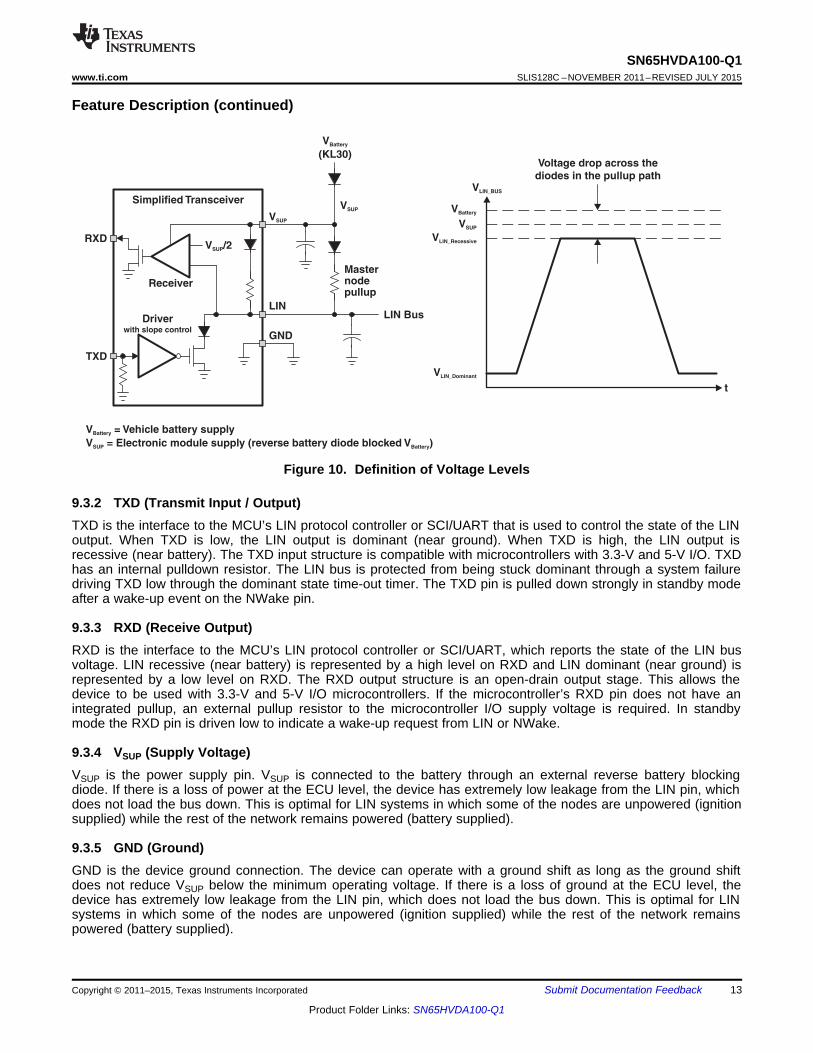
Simplified Transceiver
RXD
TXD
GND
LIN
VSUP
LIN Bus
Masternodepullup
VSUP
V
(KL30)Battery
Receiver
Driverwith slope control
V /2SUP
V = Vehicle battery supply
V = Electronic module supply (reverse battery diode blocked V )Battery
SUP Battery
VLIN_Dominant
VLIN_Recessive
VBattery
VSUP
Voltage drop across thediodes in the pullup path
t
VLIN_BUS
SN65HVDA100-Q1www.ti.com SLIS128C –NOVEMBER 2011–REVISED JULY 2015
Feature Description (continued)
Figure 10. Definition of Voltage Levels
9.3.2 TXD (Transmit Input / Output)TXD is the interface to the MCU’s LIN protocol controller or SCI/UART that is used to control the state of the LINoutput. When TXD is low, the LIN output is dominant (near ground). When TXD is high, the LIN output isrecessive (near battery). The TXD input structure is compatible with microcontrollers with 3.3-V and 5-V I/O. TXDhas an internal pulldown resistor. The LIN bus is protected from being stuck dominant through a system failuredriving TXD low through the dominant state time-out timer. The TXD pin is pulled down strongly in standby modeafter a wake-up event on the NWake pin.
9.3.3 RXD (Receive Output)RXD is the interface to the MCU’s LIN protocol controller or SCI/UART, which reports the state of the LIN busvoltage. LIN recessive (near battery) is represented by a high level on RXD and LIN dominant (near ground) isrepresented by a low level on RXD. The RXD output structure is an open-drain output stage. This allows thedevice to be used with 3.3-V and 5-V I/O microcontrollers. If the microcontroller’s RXD pin does not have anintegrated pullup, an external pullup resistor to the microcontroller I/O supply voltage is required. In standbymode the RXD pin is driven low to indicate a wake-up request from LIN or NWake.
9.3.4 VSUP (Supply Voltage)VSUP is the power supply pin. VSUP is connected to the battery through an external reverse battery blockingdiode. If there is a loss of power at the ECU level, the device has extremely low leakage from the LIN pin, whichdoes not load the bus down. This is optimal for LIN systems in which some of the nodes are unpowered (ignitionsupplied) while the rest of the network remains powered (battery supplied).
9.3.5 GND (Ground)GND is the device ground connection. The device can operate with a ground shift as long as the ground shiftdoes not reduce VSUP below the minimum operating voltage. If there is a loss of ground at the ECU level, thedevice has extremely low leakage from the LIN pin, which does not load the bus down. This is optimal for LINsystems in which some of the nodes are unpowered (ignition supplied) while the rest of the network remainspowered (battery supplied).
Copyright © 2011–2015, Texas Instruments Incorporated Submit Documentation Feedback 13
Product Folder Links: SN65HVDA100-Q1
SN65HVDA100-Q1SLIS128C –NOVEMBER 2011–REVISED JULY 2015 www.ti.com
Feature Description (continued)9.3.6 EN (Enable Input)EN controls the operational modes of the device. When EN is high, the device is in normal mode, allowing atransmission path from TXD to LIN and from LIN to RXD. When EN is low, the device is put into sleep mode andthere are no transmission paths available. The device can enter normal mode only after wake up. EN has aninternal pulldown resistor to ensure the device remains in low-power mode even if EN floats.
9.3.7 NWake (High Voltage Wake Up Input)NWake is a high-voltage input used to wake up from sleep mode. NWake is usually connected to an externalswitch in the application. A low on NWake that is asserted longer than the filter time (tNWAKE) results in a localwakeup. NWake provides an internal pullup source to VSUP.
9.3.8 INH (Inhibit Output)INH is used to control an external voltage regulator that has an inhibit or enable input. When the device is innormal operating mode, the inhibit switch is enabled and the external voltage regulator is activated. When deviceis in sleep mode, the inhibit switch is disabled, which turns off the system voltage regulator. A wake-up eventtransitions the device to standby by mode and re-enables INH which, in turn, restarts the system by turning onthe voltage regulators. INH can also drive an external transistor connected to an MCU interrupt input.
9.3.9 TXD Dominant State TimeoutDuring normal mode, if TXD is inadvertently driven permanently low by a hardware or software applicationfailure, the LIN bus is protected by the dominant state timeout timer. This timer is triggered by a falling edge onTXD. If the low signal remains on TXD for longer than tDST, the transmitter is disabled, thus allowing the LIN busto return to the recessive state and communication to resume on the bus. The protection is cleared and the tDSTtimer is reset by a rising edge on TXD. The TXD pin has an internal pulldown to ensure the device fails to aknown state if TXD is disconnected. During this fault, the transceiver remains in normal mode (assuming nochange of state request on EN), the transmitter is disabled, the RXD pin reflects the LIN bus, INH remains on,and the LIN bus pullup termination remains on.
APPLICATION HINT: The maximum dominant TXD time allowed by the TXD Dominant state time-out limitsthe minimum possible data rate of the device. The LIN protocol has different constraints for master and slaveapplications thus there are different maximum consecutive dominant bits for each application case and thusdifferent minimum data rates.
Master node: The maximum continuous dominant is the maximum dominant of the SYNC BREAKFIELD, tSYNC_DOM(max). The SYN BREAK FIELD notifies the 'start of frame' to all LIN slaves. It consists of13 to 26 dominant bits (low phase) followed by a delimiter. Thus the minimum TXD dominant time out,tDST(min) and the maximum SYNC BREAK FIELD for the master determine the minimum data rate for amaster node, which may be calculated by the following equation:DataRateMaster(min) = tSYNC_DOM(max) / tDST(min)Slave node: sends the response part of the LIN message frame which has a maximum consecutivedominant length of 9 bits (start bit + 8 data bits). As a result the minimum baud rate of a slave can becalculated by the following equation:DataRateSlave(min) = 9 + nmargin / tDST(min) where nmargin is a saftey margin.
9.3.10 Thermal ShutdownThe LIN transmitter is protected through a current limit, however, if the junction temperature of the deviceexceeds the thermal shutdown threshold, the device turns off the LIN transmitter circuit. Once theovertemperature fault condition has been removed and the junction temperature has cooled beyond thehysteresis temperature, the transmitter is re-enabled, assuming the device remained in the normal mode. Duringthis fault, the transceiver remains in normal mode (assuming no change of state request on EN), the transmitteris disabled, the RXD pin reflects the LIN bus, INH remains on, and the LIN bus pullup termination remains on.
14 Submit Documentation Feedback Copyright © 2011–2015, Texas Instruments Incorporated
Product Folder Links: SN65HVDA100-Q1

INH
LIN Bus
EN
tLINBUS
<tCLEAR
tLINBUS
tCLEAR
tLINBUS
INH
LIN Bus
EN
<tLINBUS
<tLINBUS
tLINBUS
<tLINBUS
SN65HVDA100-Q1www.ti.com SLIS128C –NOVEMBER 2011–REVISED JULY 2015
Feature Description (continued)9.3.11 Bus Stuck Dominant System Fault: False Wake-Up LockoutThe device contains logic to detect bus stuck dominant system faults and prevent the device from waking upfalsely during this system fault. Upon entering sleep mode, the device detects the state of the LIN bus. If the busis dominant, the wake-up logic is locked out until a valid recessive on the bus "clears" the bus stuck dominantcondition. This logic prevents the potential for a cyclical false wakeup of the system if the bus is stuck dominant,preventing excessive current use. Figure 11 and Figure 12 show the behavior of this protection feature.
Figure 11. No Bus Fault: Entering Sleep Mode With Bus Recessive Condition and Wakeup
Figure 12. Bus Fault: Entering Sleep Mode With Bus Stuck Dominant Fault, Clearing, and Wakeup
9.3.12 Undervoltage on VSUP
The device contains a power-on reset circuit to avoid false bus messages during undervoltage conditions whenVSUP is less than UVVSUP.
9.3.13 Unpowered Device Does Not Affect the LIN BusThe device has extremely low unpowered leakage current from the bus, so an unpowered node does not affectthe network or load it down. This is optimal for LIN systems in which some of the nodes are unpowered (ignitionsupplied) while the rest of the network remains powered (battery supplied).
Copyright © 2011–2015, Texas Instruments Incorporated Submit Documentation Feedback 15
Product Folder Links: SN65HVDA100-Q1

Unpowered System
V Vsup sup_under£
Standby Mode
Driver : OffRXD: Low
INH: High (On)Termination: 30 kW
EN = high
EN = low
EN = highLIN Bus Wake-Up
orNwake Pin Wake-Up
V Vsup sup_under£
V V
EN = lowsup sup_under>V Vsup sup_under£
V Vsup sup_under£V > V
EN = highsup sup_under
Sleep Mode
Driver : OffRXD: Floating
INH: High impedance (Off)Termination: Weak pullup
Normal Mode
Driver : OnRXD: LIN bus data
INH: High (On)Termination: 30 kW
SN65HVDA100-Q1SLIS128C –NOVEMBER 2011–REVISED JULY 2015 www.ti.com
9.4 Device Functional Modes
9.4.1 Operating States
Figure 13. Operating States Diagram
Table 1. Operating ModesLIN BUSMODE EN RXD INH TRANSMITTER COMMENTSTERMINATION
Sleep Low Floating Weak current pullup High impedance OffWake-up event detected, waitingStandby Low Low 30 kΩ (typical) High Off on MCU to set EN
Normal High LIN bus data 30 kΩ (typical) High On LIN transmission up to 20 kbps
9.4.2 Normal ModeThis is the normal operational mode, in which the receiver and driver are active, and LIN transmission up to theLIN specified maximum of 20 kbps is supported. The receiver detects the data stream on the LIN bus andoutputs it on RXD for the LIN controller, where recessive on the LIN bus is a digital high, and dominate on theLIN bus is digital low. The driver transmits input data on TXD to the LIN bus. Normal mode is entered as ENtransitions high while the SN65HVDA100 is in sleep or standby mode.
16 Submit Documentation Feedback Copyright © 2011–2015, Texas Instruments Incorporated
Product Folder Links: SN65HVDA100-Q1

SN65HVDA100-Q1www.ti.com SLIS128C –NOVEMBER 2011–REVISED JULY 2015
9.4.3 Sleep ModeSleep mode is the power saving mode for the SN65HVDA100. Even with the extremely low current consumptionin this mode, the SN65HVDA100 can still wake up from LIN bus through a wake-up signal, a low on NWake, or ifEN is set high. The LIN bus and NWake are filtered to prevent false wake-up events. The wake-up events mustbe active for their respective time periods (tLINBUS, tNWake).
The sleep mode is entered by setting EN low.
While the device is in sleep mode, the following conditions exist:• The LIN bus driver is disabled and the internal LIN bus termination is switched off (to minimize power loss if
LIN is short circuited to ground). However, the weak current pullup is active to prevent false wake-up eventsin case an external connection to the LIN bus is lost.
• The normal receiver is disabled.• INH is high impedance.• EN input, NWake input, and the LIN wake-up receiver are active.
9.4.4 Wake-Up EventsThere are three ways to wake up from sleep mode:• Remote wakeup through recessive (high) to dominant (low) state transition on LIN bus. The dominant state
must be held for tLINBUS filter time and then the bus must return to the recessive state (to eliminate falsewakeups from disturbances on the LIN bus or if the bus is shorted to ground).
• Local wakeup through a low on NWake, which is asserted low longer than the filter time tNWake (to eliminatefalse wakeups from disturbances on NWake).
• Local wakeup through EN being set high.
9.4.4.1 Wake-Up Request (RXD)When the device encounters a wake-up event from the LIN bus or NWake pin, RXD goes low, and the devicetransitions to standby mode (until EN is reasserted high and the device enters normal mode). Once the deviceenters normal mode, the RXD pin is releasing the wake-up request signal, and the RXD pin then reflects thereceiver output from the bus.
9.4.4.2 Wake-Up Source Recognition (TXD)When the device encounters a wake-up event from the LIN bus or NWake pin, TXD indicates the source whilethe device enters and remains in standby mode (until EN is reasserted high and the device enters normal mode).In addition to the internal pullup resistor on TXD, typically an external pullup resistor (approximately 5 kΩ) is usedin the system's I/O supply voltage. A high on TXD in standby mode indicates a remote wakeup through the LINbus, and a low (strong pulldown) on the TXD pin indicates a local wakeup through the NWAKE pin.
9.4.5 Standby ModeThis mode is entered whenever a wake-up event occurs through LIN bus or NWake while the device is in sleepmode. The LIN bus slave termination circuit and INH are turned on when standby mode is entered. Theapplication system powers up once INH is turned on, assuming the system is using a voltage regulatorconnected through INH. Standby mode is signaled through a low level on RXD.
When EN is set high while the device is in standby mode the device returns to normal mode and the normaltransmission paths from TXD to LIN bus and LIN bus to RXD are enabled.
During power up if EN is low the device goes into Standby mode and if EN is high the device goes into Normalmode. EN has an internal pulldown resistor, so if the pin is floating in the system, the internal pulldown willensure it is pulled low.
APPLICATION HINT: If the INH output of the SN65HVDA100 is not used to control the system powermanagement (voltage regulators) and monitor wake-up sources, but sleep mode is used to reduce systemcurrent the RXD pin can be monitored to ensure SN65HVDA100 remains in sleep mode. If the SN65HVDA100detects an undervoltage on VSUP the RXD pin transitions low and would signal to the software that theSN65HVDA100 is in standby mode and should be returned to sleep mode to return to the lowest power state.
Copyright © 2011–2015, Texas Instruments Incorporated Submit Documentation Feedback 17
Product Folder Links: SN65HVDA100-Q1
SN65HVDA100-Q1SLIS128C –NOVEMBER 2011–REVISED JULY 2015 www.ti.com
9.4.6 Mode TransitionsWhen the device is transitioning between modes the device needs the time, tMODE_CHANGE, to allow the change tofully propagate from the EN pin through the device into the new state.
APPLICATION HINT: When using the SN65HVDA100 in systems which are not controlled through the INHoutput, but rather are monitoring the RXD pin for a wake-up request, special care should be taken during themode transitions. The output of the RXD pin is indeterminate for the transition period between states as thereceivers are switched. The application software should not look for an edge on the RXD pin indicating a wake-up request until tMODE_CHANGE. This is shown in Figure 3.
10 Application and Implementation
NOTEInformation in the following applications sections is not part of the TI componentspecification, and TI does not warrant its accuracy or completeness. TI’s customers areresponsible for determining suitability of components for their purposes. Customers shouldvalidate and test their design implementation to confirm system functionality.
10.1 Application InformationThe SN65HVDA100-Q1 can be used as both a slave device and a master device in a LIN network. The devicecomes with the ability to support both remote wake-up requests and local wake-up requests.
10.2 Typical ApplicationThe device comes with an integrated 30-kΩ pullup resistor and series diode for slave applications, and for masterapplications an external 1-kΩ pullup with series blocking diode can be used. Figure 14 shows the device beingused in both types of applications.
18 Submit Documentation Feedback Copyright © 2011–2015, Texas Instruments Incorporated
Product Folder Links: SN65HVDA100-Q1

VBAT
VSUP
VDD
VDD
VSUPINH
NWake
SN65HVDA100-Q1MCU
MASTERNODE
TMS470
LINController
orSCI/UART(1)
EN
RXD
TXD
MCU w/opullup (2)
VDD I/O
GND
28 3 7
1
4 5
6
MasterNode
Pullup(3)
1 k
LIN
220 pF
VSUP
TPSxxxx
VSUP
VDD
VDD
VSUPINH
NWake
SN65HVDA100-Q1MCU
TMS470
LINController
orSCI/UART(1)
EN
TXD
MCU w/opullup(2)
VDD I/O
GND
28 3 7
1
4 5
6LIN
220 pF
RXD
SLAVENODE
LIN
Bu
s
I/O
I/O
TPSxxxx
VSUP
VDD
SN65HVDA100-Q1www.ti.com SLIS128C –NOVEMBER 2011–REVISED JULY 2015
Typical Application (continued)
(1) RXD on MCU or LIN slave has internal pullup, no external pullup resistor is needed.(2) RXD on MCU or LIN slave without internal pullup, requires external pullup resistor.(3) Master node applications require an external 1-kΩ pullup resistor and serial diode.
Figure 14. SN65HVDA100-Q1 Application Diagram
10.2.1 Design RequirementsFor this design, use these requirements:
1. RXD on MCU or LIN Slave has internal pullup, no external pullup resistor is needed.
2. RXD on MCU or LIN Slave without internal pullup, requires external pullup resistor.
3. Master Node applications require an external 1-kΩ pullup resistor and serial diode.
Copyright © 2011–2015, Texas Instruments Incorporated Submit Documentation Feedback 19
Product Folder Links: SN65HVDA100-Q1
SN65HVDA100-Q1SLIS128C –NOVEMBER 2011–REVISED JULY 2015 www.ti.com
Typical Application (continued)10.2.2 Detailed Design ProcedureThe RXD output structure is an open-drain output stage. This allows the SN65HVDA100-Q1 to be used with 3.3-V and 5-V I/O microcontrollers. If the RXD pin of the microcontroller does not have an integrated pullup, anexternal pullup resistor to the microcontroller I/O supply voltage is required.
The VSUP pin of the device should be decoupled with a 100-nF capacitor as close to the supply pin of the deviceas possible.
The NWAKE pin is a high voltage wake-up input to the device. If this pin is not being used it should be tied toVSUP.
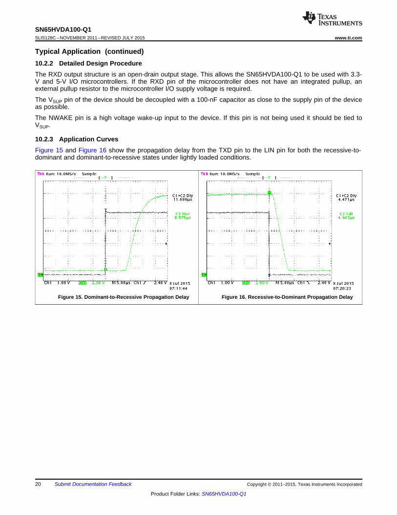
10.2.3 Application CurvesFigure 15 and Figure 16 show the propagation delay from the TXD pin to the LIN pin for both the recessive-to-dominant and dominant-to-recessive states under lightly loaded conditions.
Figure 15. Dominant-to-Recessive Propagation Delay Figure 16. Recessive-to-Dominant Propagation Delay
20 Submit Documentation Feedback Copyright © 2011–2015, Texas Instruments Incorporated
Product Folder Links: SN65HVDA100-Q1
SN65HVDA100-Q1www.ti.com SLIS128C –NOVEMBER 2011–REVISED JULY 2015
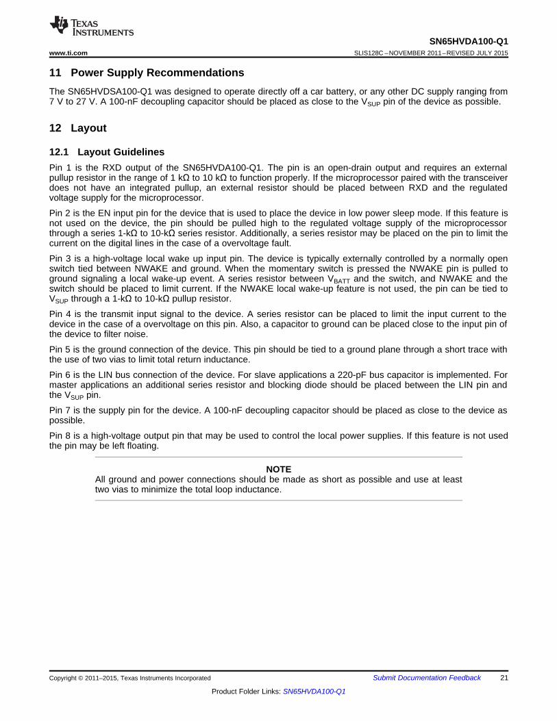
11 Power Supply RecommendationsThe SN65HVDSA100-Q1 was designed to operate directly off a car battery, or any other DC supply ranging from7 V to 27 V. A 100-nF decoupling capacitor should be placed as close to the VSUP pin of the device as possible.
12 Layout
12.1 Layout GuidelinesPin 1 is the RXD output of the SN65HVDA100-Q1. The pin is an open-drain output and requires an externalpullup resistor in the range of 1 kΩ to 10 kΩ to function properly. If the microprocessor paired with the transceiverdoes not have an integrated pullup, an external resistor should be placed between RXD and the regulatedvoltage supply for the microprocessor.
Pin 2 is the EN input pin for the device that is used to place the device in low power sleep mode. If this feature isnot used on the device, the pin should be pulled high to the regulated voltage supply of the microprocessorthrough a series 1-kΩ to 10-kΩ series resistor. Additionally, a series resistor may be placed on the pin to limit thecurrent on the digital lines in the case of a overvoltage fault.
Pin 3 is a high-voltage local wake up input pin. The device is typically externally controlled by a normally openswitch tied between NWAKE and ground. When the momentary switch is pressed the NWAKE pin is pulled toground signaling a local wake-up event. A series resistor between VBATT and the switch, and NWAKE and theswitch should be placed to limit current. If the NWAKE local wake-up feature is not used, the pin can be tied toVSUP through a 1-kΩ to 10-kΩ pullup resistor.
Pin 4 is the transmit input signal to the device. A series resistor can be placed to limit the input current to thedevice in the case of a overvoltage on this pin. Also, a capacitor to ground can be placed close to the input pin ofthe device to filter noise.
Pin 5 is the ground connection of the device. This pin should be tied to a ground plane through a short trace withthe use of two vias to limit total return inductance.
Pin 6 is the LIN bus connection of the device. For slave applications a 220-pF bus capacitor is implemented. Formaster applications an additional series resistor and blocking diode should be placed between the LIN pin andthe VSUP pin.
Pin 7 is the supply pin for the device. A 100-nF decoupling capacitor should be placed as close to the device aspossible.
Pin 8 is a high-voltage output pin that may be used to control the local power supplies. If this feature is not usedthe pin may be left floating.
NOTEAll ground and power connections should be made as short as possible and use at leasttwo vias to minimize the total loop inductance.
Copyright © 2011–2015, Texas Instruments Incorporated Submit Documentation Feedback 21
Product Folder Links: SN65HVDA100-Q1

1
2
3
4
U1SN65HVDA100-Q1
8
7
6
5
C2R3
R2
GND
EN
R6
R7 INH
D3
RXD
TXD
R1
C1
VC
R5
R4
VC
VSUP
GND
GND GND
D1
D2
R7 Only needed for
the master node
VSUP
C3
GND
SN65HVDA100-Q1SLIS128C –NOVEMBER 2011–REVISED JULY 2015 www.ti.com
12.2 Layout Example
Figure 17. Layout Schematic
22 Submit Documentation Feedback Copyright © 2011–2015, Texas Instruments Incorporated
Product Folder Links: SN65HVDA100-Q1

SN65HVDA100-Q1www.ti.com SLIS128C –NOVEMBER 2011–REVISED JULY 2015
13 Device and Documentation Support
13.1 Community ResourcesThe following links connect to TI community resources. Linked contents are provided "AS IS" by the respectivecontributors. They do not constitute TI specifications and do not necessarily reflect TI's views; see TI's Terms ofUse.
TI E2E™ Online Community TI's Engineer-to-Engineer (E2E) Community. Created to foster collaborationamong engineers. At e2e.ti.com, you can ask questions, share knowledge, explore ideas and helpsolve problems with fellow engineers.
Design Support TI's Design Support Quickly find helpful E2E forums along with design support tools andcontact information for technical support.
13.2 TrademarksE2E is a trademark of Texas Instruments.All other trademarks are the property of their respective owners.
13.3 Electrostatic Discharge CautionThese devices have limited built-in ESD protection. The leads should be shorted together or the device placed in conductive foamduring storage or handling to prevent electrostatic damage to the MOS gates.
13.4 GlossarySLYZ022 — TI Glossary.
This glossary lists and explains terms, acronyms, and definitions.
14 Mechanical, Packaging, and Orderable InformationThe following pages include mechanical, packaging, and orderable information. This information is the mostcurrent data available for the designated devices. This data is subject to change without notice and revision ofthis document. For browser-based versions of this data sheet, refer to the left-hand navigation.
Copyright © 2011–2015, Texas Instruments Incorporated Submit Documentation Feedback 23
Product Folder Links: SN65HVDA100-Q1

PACKAGE OPTION ADDENDUM
www.ti.com 10-Dec-2020
Addendum-Page 1
PACKAGING INFORMATION
Orderable Device Status(1)
Package Type PackageDrawing
Pins PackageQty
Eco Plan(2)
Lead finish/Ball material
(6)
MSL Peak Temp(3)
Op Temp (°C) Device Marking(4/5)
Samples
SN65HVDA100QDRQ1 ACTIVE SOIC D 8 2500 RoHS & Green NIPDAU Level-2-260C-1 YEAR -40 to 125 A100Q
(1) The marketing status values are defined as follows:ACTIVE: Product device recommended for new designs.LIFEBUY: TI has announced that the device will be discontinued, and a lifetime-buy period is in effect.NRND: Not recommended for new designs. Device is in production to support existing customers, but TI does not recommend using this part in a new design.PREVIEW: Device has been announced but is not in production. Samples may or may not be available.OBSOLETE: TI has discontinued the production of the device.
(2) RoHS: TI defines "RoHS" to mean semiconductor products that are compliant with the current EU RoHS requirements for all 10 RoHS substances, including the requirement that RoHS substancedo not exceed 0.1% by weight in homogeneous materials. Where designed to be soldered at high temperatures, "RoHS" products are suitable for use in specified lead-free processes. TI mayreference these types of products as "Pb-Free".RoHS Exempt: TI defines "RoHS Exempt" to mean products that contain lead but are compliant with EU RoHS pursuant to a specific EU RoHS exemption.Green: TI defines "Green" to mean the content of Chlorine (Cl) and Bromine (Br) based flame retardants meet JS709B low halogen requirements of <=1000ppm threshold. Antimony trioxide basedflame retardants must also meet the <=1000ppm threshold requirement.
(3) MSL, Peak Temp. - The Moisture Sensitivity Level rating according to the JEDEC industry standard classifications, and peak solder temperature.
(4) There may be additional marking, which relates to the logo, the lot trace code information, or the environmental category on the device.
(5) Multiple Device Markings will be inside parentheses. Only one Device Marking contained in parentheses and separated by a "~" will appear on a device. If a line is indented then it is a continuationof the previous line and the two combined represent the entire Device Marking for that device.
(6) Lead finish/Ball material - Orderable Devices may have multiple material finish options. Finish options are separated by a vertical ruled line. Lead finish/Ball material values may wrap to twolines if the finish value exceeds the maximum column width.
Important Information and Disclaimer:The information provided on this page represents TI's knowledge and belief as of the date that it is provided. TI bases its knowledge and belief on informationprovided by third parties, and makes no representation or warranty as to the accuracy of such information. Efforts are underway to better integrate information from third parties. TI has taken andcontinues to take reasonable steps to provide representative and accurate information but may not have conducted destructive testing or chemical analysis on incoming materials and chemicals.TI and TI suppliers consider certain information to be proprietary, and thus CAS numbers and other limited information may not be available for release.
In no event shall TI's liability arising out of such information exceed the total purchase price of the TI part(s) at issue in this document sold by TI to Customer on an annual basis.

TAPE AND REEL INFORMATION
*All dimensions are nominal
Device PackageType
PackageDrawing
Pins SPQ ReelDiameter
(mm)
ReelWidth
W1 (mm)
A0(mm)
B0(mm)
K0(mm)
P1(mm)
W(mm)
Pin1Quadrant
SN65HVDA100QDRQ1 SOIC D 8 2500 330.0 12.4 6.4 5.2 2.1 8.0 12.0 Q1
PACKAGE MATERIALS INFORMATION
www.ti.com 16-Oct-2020
Pack Materials-Page 1

*All dimensions are nominal
Device Package Type Package Drawing Pins SPQ Length (mm) Width (mm) Height (mm)
SN65HVDA100QDRQ1 SOIC D 8 2500 853.0 449.0 35.0
PACKAGE MATERIALS INFORMATION
www.ti.com 16-Oct-2020
Pack Materials-Page 2

www.ti.com
PACKAGE OUTLINE
C
.228-.244 TYP[5.80-6.19]
.069 MAX[1.75]
6X .050[1.27]
8X .012-.020 [0.31-0.51]
2X.150[3.81]
.005-.010 TYP[0.13-0.25]
0 - 8 .004-.010[0.11-0.25]
.010[0.25]
.016-.050[0.41-1.27]
4X (0 -15 )
A
.189-.197[4.81-5.00]
NOTE 3
B .150-.157[3.81-3.98]
NOTE 4
4X (0 -15 )
(.041)[1.04]
SOIC - 1.75 mm max heightD0008ASMALL OUTLINE INTEGRATED CIRCUIT
4214825/C 02/2019
NOTES: 1. Linear dimensions are in inches [millimeters]. Dimensions in parenthesis are for reference only. Controlling dimensions are in inches. Dimensioning and tolerancing per ASME Y14.5M. 2. This drawing is subject to change without notice. 3. This dimension does not include mold flash, protrusions, or gate burrs. Mold flash, protrusions, or gate burrs shall not exceed .006 [0.15] per side. 4. This dimension does not include interlead flash.5. Reference JEDEC registration MS-012, variation AA.
18
.010 [0.25] C A B
54
PIN 1 ID AREA
SEATING PLANE
.004 [0.1] C
SEE DETAIL A
DETAIL ATYPICAL
SCALE 2.800

www.ti.com
EXAMPLE BOARD LAYOUT
.0028 MAX[0.07]ALL AROUND
.0028 MIN[0.07]ALL AROUND
(.213)[5.4]
6X (.050 )[1.27]
8X (.061 )[1.55]
8X (.024)[0.6]
(R.002 ) TYP[0.05]
SOIC - 1.75 mm max heightD0008ASMALL OUTLINE INTEGRATED CIRCUIT
4214825/C 02/2019
NOTES: (continued) 6. Publication IPC-7351 may have alternate designs. 7. Solder mask tolerances between and around signal pads can vary based on board fabrication site.
METALSOLDER MASKOPENING
NON SOLDER MASKDEFINED
SOLDER MASK DETAILS
EXPOSEDMETAL
OPENINGSOLDER MASK METAL UNDER
SOLDER MASK
SOLDER MASKDEFINED
EXPOSEDMETAL
LAND PATTERN EXAMPLEEXPOSED METAL SHOWN
SCALE:8X
SYMM
1
45
8
SEEDETAILS
SYMM

www.ti.com
EXAMPLE STENCIL DESIGN
8X (.061 )[1.55]
8X (.024)[0.6]
6X (.050 )[1.27]
(.213)[5.4]
(R.002 ) TYP[0.05]
SOIC - 1.75 mm max heightD0008ASMALL OUTLINE INTEGRATED CIRCUIT
4214825/C 02/2019
NOTES: (continued) 8. Laser cutting apertures with trapezoidal walls and rounded corners may offer better paste release. IPC-7525 may have alternate design recommendations. 9. Board assembly site may have different recommendations for stencil design.
SOLDER PASTE EXAMPLEBASED ON .005 INCH [0.125 MM] THICK STENCIL
SCALE:8X
SYMM
SYMM
1
45
8
IMPORTANT NOTICE AND DISCLAIMER
TI PROVIDES TECHNICAL AND RELIABILITY DATA (INCLUDING DATASHEETS), DESIGN RESOURCES (INCLUDING REFERENCE DESIGNS), APPLICATION OR OTHER DESIGN ADVICE, WEB TOOLS, SAFETY INFORMATION, AND OTHER RESOURCES “AS IS” AND WITH ALL FAULTS, AND DISCLAIMS ALL WARRANTIES, EXPRESS AND IMPLIED, INCLUDING WITHOUT LIMITATION ANY IMPLIED WARRANTIES OF MERCHANTABILITY, FITNESS FOR A PARTICULAR PURPOSE OR NON-INFRINGEMENT OF THIRD PARTY INTELLECTUAL PROPERTY RIGHTS.These resources are intended for skilled developers designing with TI products. You are solely responsible for (1) selecting the appropriate TI products for your application, (2) designing, validating and testing your application, and (3) ensuring your application meets applicable standards, and any other safety, security, or other requirements. These resources are subject to change without notice. TI grants you permission to use these resources only for development of an application that uses the TI products described in the resource. Other reproduction and display of these resources is prohibited. No license is granted to any other TI intellectual property right or to any third party intellectual property right. TI disclaims responsibility for, and you will fully indemnify TI and its representatives against, any claims, damages, costs, losses, and liabilities arising out of your use of these resources.TI’s products are provided subject to TI’s Terms of Sale (www.ti.com/legal/termsofsale.html) or other applicable terms available either on ti.com or provided in conjunction with such TI products. TI’s provision of these resources does not expand or otherwise alter TI’s applicable warranties or warranty disclaimers for TI products.
Mailing Address: Texas Instruments, Post Office Box 655303, Dallas, Texas 75265Copyright © 2020, Texas Instruments Incorporated