smart battery charger with smbus interface - t-es-t.hu · smart battery charger. the demo board,...
TRANSCRIPT

Smart Battery Charger with SMBus Interface
AN667
INTRODUCTION
This application note provides the schematics, softwarelistings, and circuit board layout for a PIC16C73 basedSmart Battery Charger. The Demo Board, DC101, isavailable to selected customers through Linear Tech-nology Corp. product marketing.
The DC101 (Figure 1) is the Smart Battery Charger(SBC) portion of a Smart Battery System. A simplifiedblock diagram of a Smart Battery System is shown inFigure 3 (refer to "The Smart Battery Charger Specifi-cation," Duracell).
Authors: Laszlo Kiraly, Linear Technology
Robert Schreiber, Microchip Technology
1997 Microchip Technology Inc.
The Smart Battery (SB) contains circuitry which pro-vides charging information to the SBC. The SBCreceives this information in terms of ChargingVoltage(),ChargingCurrent(), and AlarmWarning() commandsfrom the SB. The SBC and SB communicate via theSystem Management Bus (SMB), which is an imple-mentation of the I2C bus (refer to "The Smart Manage-ment Bus Specification," Intel; and "The I2C Bus andHow to Use It," Philips Semiconductor). The SBC setsthe charging current and voltage based on input fromthe SB. The SBC charger also has the intelligence tomonitor the SB’s thermistor. The thermistor providestemperature information for charge termination, andbattery chemistry information.
FIGURE 1: DC101 SMART BATTERY CHARGER
FIGURE 2: SIMPLIFIED BLOCK DIAGRAM
SmartBatteryCharger
Vbattery
Thermistor
SMBus
SmartBattery
DS00667A-page 1

AN667
FIGURE 3: BLOCK DIAGRAM
From
LT1129
LT1511
Charger
PIC16C72/PIC16C73
+5V
26
11
13
12
14
15
2Shutdown
Voltage PWM
Current PWM
Q2
Q1
Q3
DC101CSmart Battery Charger
µP
+5V
SMB
DCOK
R10
+
-
DC OutTo System
GND
(+)
C SMBus Clock (SCL)
D SMBus Data (SDA)
T Thermistor
(-)Battery Charger
System Current
WallCube
OPERATING THE BOARD
Input voltage. The nominal input voltage of the boardis 24V DC (Refer to Appendix A for Performance Sum-mary). The input voltage must be higher than the bat-tery voltage by a minimum of 3V. The minimum inputvoltage is 16V, limited by the undervoltage lockout cir-cuit in the LT1511 and set by resistors R16, R17 andR18. The highest input voltage is 27.4V, that is limitedby the maximum input voltage of the LT1511. The inputis protected against reverse polarity up to 30V.
Input current. The sum of the system current and thecharger input current is limited by the LT1511 to 2A.When both the system current and the charger inputcurrent requirements are high, the charger reduces thecharging current to meet the 2A current limit.
RED LED. It indicates SMBus activity. It lights-up forabout 1 second when the charger recognizes its ownaddress (12hex) on the SMBus.
Green LED. Flashing green LED indicates micropro-cessor activity and charger status.
Fast blinking (approximately 8 Hz) indicates normalmicroprocessor activity and either trickle charge or shutdown charger status. After valid voltage and currentdata have been received the blinking speed of the LEDslows down to about 2 Hz, indicating normal charging.
DS00667A-page 2
Battery removal, thermistor measurements. Thecharger periodically checks the thermistor in the batterythrough the T terminal. When the thermistor is out ofnormal operating temperature range, the chargerswitches to trickle charge mode and increases theflashing frequency of the green LED to indicate anabnormal charging condition. When the resistance ofthe thermistor is in the 500Ω < Rth < 1.5 kΩ range, thecharger assumes Li Ion battery is at the output, andinstead of trickle charging the battery it shuts-down thecharger until a valid voltage and current request arrivesfrom the battery.
An open thermistor forces the charger into tricklecharge mode and the charger disregards data on theSMBus.
The schematics, parts list, and circuit layout are shownin Appendix A.
1997 Microchip Technology Inc.

AN667
SYSTEM MANAGEMENT BUS (SMBUS)
When charge in the Smart Battery (SB) drops below85% of the nominal capacity, it initiates communicationover the SMBus every 64 seconds. After sending aSTART sequence the battery addresses the Smart Bat-tery charger and waits for acknowledgment (ACK) fromit. If the charger fails to acknowledge the word, the bat-tery terminates further communication by placing aSTOP sequence onto the SMBus. If the chargeracknowledges (ACK) the reception of first word, thebattery continues the communication sequence and itsends six more words to the charger. The complete cur-rent and voltage request communication sequence isshown below:
START address (12 hex) ChargingCurrent() command code (14 hex), current_LSB current_MSB, address (12 hex)ChargingVoltage() command code (15 hex)voltage_LSBvoltage_MSB STOP
1997 Microchip Technology Inc.
The idealized SMBus waveforms shown in Figure 4illustrate SMBus communication between the batteryand the charger. The first seven bits after the startsequence is the battery address. The R/W tells thecharger that the battery attempts to write to the charger.
During the acknowledge period (ACK), the chargerbecomes active and it pulls the data line (SDA) low indi-cating reception of a data word. When reception of thedata word is not acknowledged by the charger, the bat-tery terminates the communication by sending a STOPsequence to the bus. The clock pulses for the commu-nication are always generated by the battery (BUSMASTER).
CONCLUSION
The PIC16C73 contains the on-board peripherals nec-essary to easily implement an SMBus battery charger.The I2C module allows for the SMBus communicationsand the PWM modules allow for voltage and currentcontrol. This high level of integration reduces the exter-nal components required and increases the flexibility ofthe design.
A complete software listing is shown in Appendix B.
FIGURE 4: SMBus WAVEFORMS
1 2 7 8 9 1 2 3 • 8 9 P
SDA
SCL S
StartCondition Address R/W ACK Wait
StateData ACK
MSB acknowledgmentsignal from receiver
acknowledgmentsignal from receiverbyte complete
interrupt with receiver
clock line held low whileinterrupts are serviced
StopCondition
DS00667A-page 3

AN667
APPENDIX A:
TABLE A-1: PERFORMANCE SUMMARY
Parameter Conditions MIN TYP MAX UNIT
Input Voltage 16.0 24.0 27.0 V
Input Current Hardware Limited 2.0 A
Output Current Software Limited 0 2.5 A
Output Voltage Software Limited 4 20 V
Thermistor Resistance NiMH Battery 3k 30k Ohms
Li Ion 500 1000 1500 Ohms
DS00667A-page 4 1997 Microchip Technology Inc.

AN667
FIGURE A-1: SCHEMATIC DIAGRAM
MC
LRR
A0/
AN
0R
A1/
AN
1R
A2/
AN
2R
A3/
AN
3R
A4
RA
5/A
N4
Vss
OS
C1
OS
C2
RC
0C
CP
2 (7
3)C
CP
1S
CL
RB
7R
B6
RB
5R
B4
RB
3R
B2
RB
1R
B0/
INT
VD
D
VS
S
RC
7R
C6
RC
5S
DA
28 27 26 25 24 23 22 21 20 19 18 17 16 15
1 2 3 4 5 6 7 8 9 10 11 12 13 14
GN
DS
WB
OO
ST
GN
DG
ND
UV
GN
DO
VP
CLP
CLN
CO
MP
1S
EN
SE
GN
DG
ND
Vcc
1V
CC
2V
cc3
PR
OG
VC
UV
OU
TG
ND
CO
MP
2B
ATS
PIN
24 23 22 21 20 19 18 17 16 15 14 13
1 2 3 4 5 6 7 8 9 10 11 12
R26
12
10k
R7
12
33.2
k, 1
%
U1
PIC
16C
73S1
R5
1 233
0
D1
RE
D(S
MB
)
R6
1 233
0
D2
GR
N(µ
P)
C1
0.1
µF50
V
2 1
1 2 3 4 5 6 7 8 9 10 11 12
JPR
1+
5V
Res
et
Cha
rger
Adj
ustm
ent
Ran
ge:
PW
M1:
3F
Fh
= 2
2.4V
000h
= 6
VP
WM
2: 3
FF
h =
4.1
A00
0h =
0A
C14
33 p
F50
V2 1
21
C15
33 p
F 5
0V2
1
Y1
4 M
Hz
Res
et
R18
21
1.00
k
+5V
1/10
W1%
R17
21
1.05
k1/
10W
1%
C11
10 µ
F25
V1 2
TOK
IN
C10
10 µ
F25
V1 2
TOK
IN
R4
12
3.32
k, 1
%
U2
R21
2 122
k5%
+5V
R22
2 122
k5%
+5V
R25
2 122
k5%
+5V
R13
2 114
3k1/
10W
0.1%
R12
2 110
0k1/
10W
0.1%
R9
1 210
0k1/
10W
5%
R1
1 23.
32k
1/10
W1%
R3
1 21.
00k
1/10
W1%
R19
21
200
1/10
W1%
R20
21
200
1/10
W1%
R14
12
330
1/10
W5%
R23
12
221/
10W
5%
R11
1 251
01/
10W 5%
R10
12
0.05
01/
2W
R16
21
3.32
k1/
10W
1%
R2
12
301
1/10
W1%
C6
0.04
7 µF
50V
1 2C7
0.01
5 µF
25V
1 2
C3
0.33
µF
25V
1 2
C16
100
pF50
V
1 2
C4
1 µF
25V
1 2
C17
0.1
µF50
V
1 2
R8
1 20.
033
2 1/
2W
C19
0.1
µF50
V
1 2
C12
10 µ
F25
V
1 2
C20
10 µ
F25
V
1 23 2
3 2
3 2
+5V
1
1
R24
12
10k
5%
C8
0.1
µF50
V1 2
C5
1 µF
25V
21
LT15
11
D3
MB
RS
340T
3
D6
BA
S16
LT1
C9
0.47
µF
25V
1 2
D4
BA
S16
LT1
13 13
+5V
C18
10 µ
F10
V
1 2+
D5
MB
RS
340T
3
C2
10 µ
F10
V
1+ 2+5V
LT11
29IS
T-5
VIN
VO
UT
G N D
T A B
E1
1
24V
@ 2
A
E2 1
Cen
ter
Pos
tis
+
J2
5%
10%
J1(+
)(+
)C
LOC
KC
LOC
KD
ATA
DAT
A(T
)(T
)(-
)(-
)
1 2 3 4 5 6 7 8 9 10
AM
P-7
8744
1-1
Sm
art
Bat
tery
Co
nn
ecto
r
E5
1
R15
21
21.5
k1/
10W
0.1%
1
Q2
2N70
02LT
1
Q1
2N70
02LT
1
Q3
2N70
02LT
1
E6
1
E7
1
TP
1 1
TP
2 1
TP
3 1
TP
4 1
TP
5 1
SM
BC
LK
SM
BD
ATA
INT
Not
es: U
nles
s ot
herw
ise
spec
ified
1: A
ll re
sist
ance
s ar
e in
Ohm
s. 1
/10W
, 5%
.2:
All
capa
cita
nces
are
in m
icro
-far
ads,
50V
, 10%
.
U3
31
Coi
ltron
ics
CT
X20
-4
20 µ
H
3 2 1 4
Q4
MM
BT
3904
LT1
DC
OU
TE
31
E4
1
24
L1
2.46
5V
Shu
tdow
n
Bol
d lin
e in
dica
tes
high
cur
rent
pat
hs
PIC
16C
72
1997 Microchip Technology Inc. DS00667A-page 5
AN667
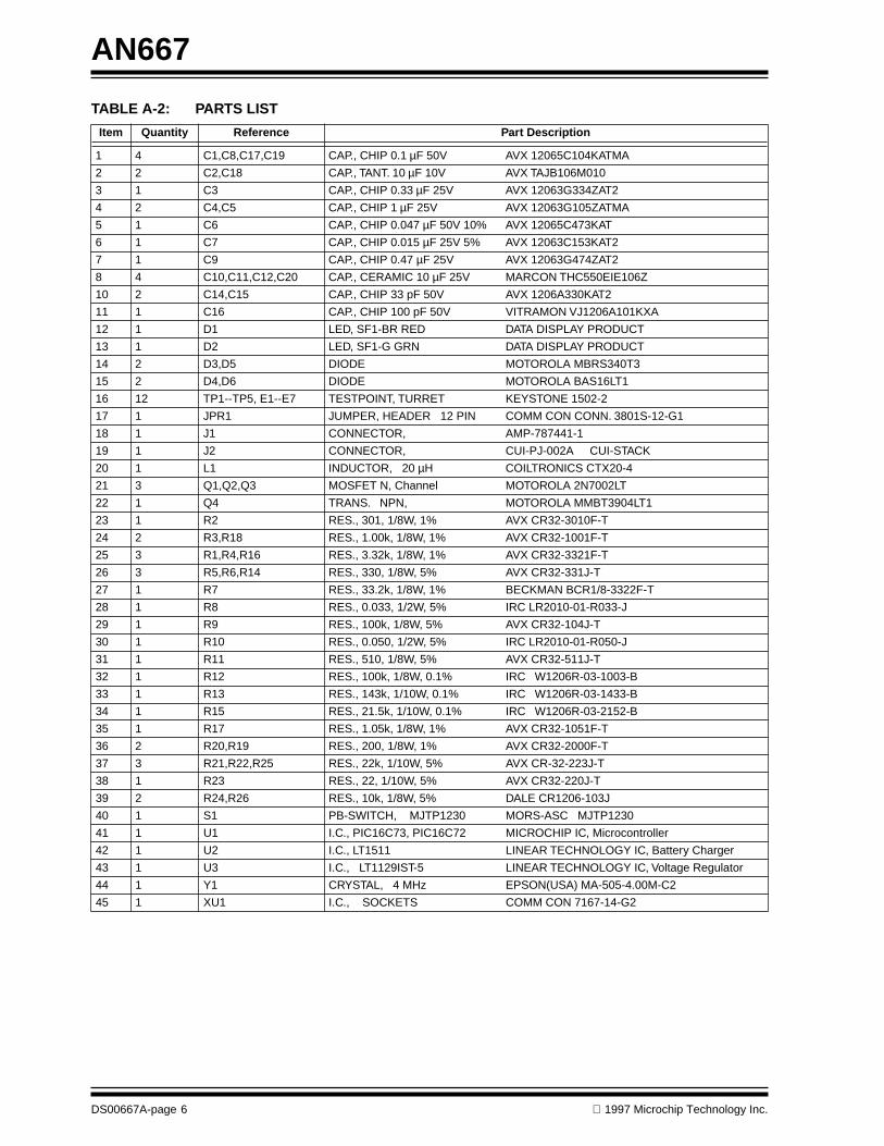
TABLE A-2: PARTS LIST
Item Quantity Reference Part Description
1 4 C1,C8,C17,C19 CAP., CHIP 0.1 µF 50V AVX 12065C104KATMA
2 2 C2,C18 CAP., TANT. 10 µF 10V AVX TAJB106M010
3 1 C3 CAP., CHIP 0.33 µF 25V AVX 12063G334ZAT2
4 2 C4,C5 CAP., CHIP 1 µF 25V AVX 12063G105ZATMA
5 1 C6 CAP., CHIP 0.047 µF 50V 10% AVX 12065C473KAT
6 1 C7 CAP., CHIP 0.015 µF 25V 5% AVX 12063C153KAT2
7 1 C9 CAP., CHIP 0.47 µF 25V AVX 12063G474ZAT2
8 4 C10,C11,C12,C20 CAP., CERAMIC 10 µF 25V MARCON THC550EIE106Z
10 2 C14,C15 CAP., CHIP 33 pF 50V AVX 1206A330KAT2
11 1 C16 CAP., CHIP 100 pF 50V VITRAMON VJ1206A101KXA
12 1 D1 LED, SF1-BR RED DATA DISPLAY PRODUCT
13 1 D2 LED, SF1-G GRN DATA DISPLAY PRODUCT
14 2 D3,D5 DIODE MOTOROLA MBRS340T3
15 2 D4,D6 DIODE MOTOROLA BAS16LT1
16 12 TP1--TP5, E1--E7 TESTPOINT, TURRET KEYSTONE 1502-2
17 1 JPR1 JUMPER, HEADER 12 PIN COMM CON CONN. 3801S-12-G1
18 1 J1 CONNECTOR, AMP-787441-1
19 1 J2 CONNECTOR, CUI-PJ-002A CUI-STACK
20 1 L1 INDUCTOR, 20 µH COILTRONICS CTX20-4
21 3 Q1,Q2,Q3 MOSFET N, Channel MOTOROLA 2N7002LT
22 1 Q4 TRANS. NPN, MOTOROLA MMBT3904LT1
23 1 R2 RES., 301, 1/8W, 1% AVX CR32-3010F-T
24 2 R3,R18 RES., 1.00k, 1/8W, 1% AVX CR32-1001F-T
25 3 R1,R4,R16 RES., 3.32k, 1/8W, 1% AVX CR32-3321F-T
26 3 R5,R6,R14 RES., 330, 1/8W, 5% AVX CR32-331J-T
27 1 R7 RES., 33.2k, 1/8W, 1% BECKMAN BCR1/8-3322F-T
28 1 R8 RES., 0.033, 1/2W, 5% IRC LR2010-01-R033-J
29 1 R9 RES., 100k, 1/8W, 5% AVX CR32-104J-T
30 1 R10 RES., 0.050, 1/2W, 5% IRC LR2010-01-R050-J
31 1 R11 RES., 510, 1/8W, 5% AVX CR32-511J-T
32 1 R12 RES., 100k, 1/8W, 0.1% IRC W1206R-03-1003-B
33 1 R13 RES., 143k, 1/10W, 0.1% IRC W1206R-03-1433-B
34 1 R15 RES., 21.5k, 1/10W, 0.1% IRC W1206R-03-2152-B
35 1 R17 RES., 1.05k, 1/8W, 1% AVX CR32-1051F-T
36 2 R20,R19 RES., 200, 1/8W, 1% AVX CR32-2000F-T
37 3 R21,R22,R25 RES., 22k, 1/10W, 5% AVX CR-32-223J-T
38 1 R23 RES., 22, 1/10W, 5% AVX CR32-220J-T
39 2 R24,R26 RES., 10k, 1/8W, 5% DALE CR1206-103J
40 1 S1 PB-SWITCH, MJTP1230 MORS-ASC MJTP1230
41 1 U1 I.C., PIC16C73, PIC16C72 MICROCHIP IC, Microcontroller
42 1 U2 I.C., LT1511 LINEAR TECHNOLOGY IC, Battery Charger
43 1 U3 I.C., LT1129IST-5 LINEAR TECHNOLOGY IC, Voltage Regulator
44 1 Y1 CRYSTAL, 4 MHz EPSON(USA) MA-505-4.00M-C2
45 1 XU1 I.C., SOCKETS COMM CON 7167-14-G2
DS00667A-page 6 1997 Microchip Technology Inc.
AN667
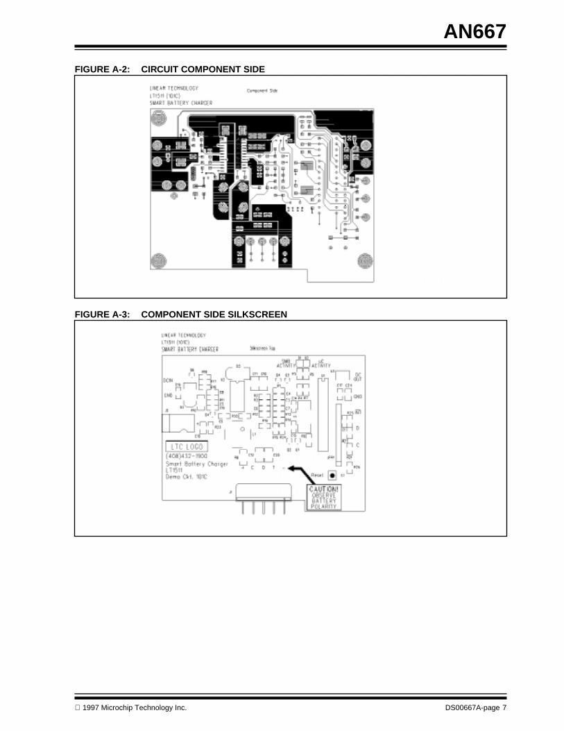
FIGURE A-2: CIRCUIT COMPONENT SIDE
FIGURE A-3: COMPONENT SIDE SILKSCREEN
1997 Microchip Technology Inc. DS00667A-page 7

AN667
FIGURE A-4: COMPONENT SIDE SOLDERSIDE
FIGURE A-5: CIRCUIT SOLDER SIDE
DS00667A-page 8 1997 Microchip Technology Inc.

AN667
FIGURE A-6: SOLDER SIDE SOLDER MASK
1997 Microchip Technology Inc. DS00667A-page 9

AN667
APPENDIX B:
FIGURE B-1: SOFTWARE FLOWCHART
Thermistor Open?
Thermistor Too Hot?
Thermistor in Range?
Thermistor Too Cold?
Li-Ion?
Thermistor Shorted
Disable Interrupts
I2C Data Received?
If Li-Ion Flag Set, START
Turn Red LED onfor 2 secondsReset I2C Pointer
A/D Counter = 0? Measure Thermistor
AlarmWarningSet Error FlagShutdown ChargerErase Command
ChargingCurrentLoad IPWMErase CommandEnable Charger
ChargingVoltage
Error Flag? Set Fast Blinking
If Li-Ion Flag Set,Erase Li-Ion FlagErase Error Flag
Interrupt
Return fromInterrupt
Put I2C Data onthe I2C Stack.Increment Pointer
Enable Interrupts
Set Trickle ChargeSet Error Flag
If Li-Ion Flag Set,Erase Li-Ion FlagErase Error Flag
If Li-Ion Flag Set,Erase Li-Ion FlagErase Error FlagInit. Ni-MH Mode
Set Trickle ChargeSet Error Flag
Set Trickle ChargeSet Error Flag
Set Trickle ChargeSet Error Flag
on Stack?
on Stack?Erase Error Flag
on Stack?
Load VPWMErase CommandEnable ChargerErase Error Flag
Yes
Yes
Yes
Yes
Yes
Yes
Yes
Yes
Yes
Yes
Yes
No
No
No
No
No
No
No
No
No
No
No
DS00667A-page 10 1997 Microchip Technology Inc.

AN667
//--------------------------------------------------------------------------// CHRGR101.C Version: 1.01// By: Laszlo Kiraly// Email:[email protected]// Linear Technology// Applications Department// 1630 McCarthy Blvd, Milpitas, CA 95035, USA // Phone: (408) 432-1900, Fax: (408) 434-0507 /*--------------------------------------------------------------------------- April 16,1996This program: Sets-up PWMs and I2C communication. It receives data from I2C (including its own address) and stores them in i2c_data[10] as they come in, including its own address (0x12).
0 charger i2c address (always 0x12) 1 ChargingCurrent() CMD (0x14) 2 charging current data byte L 3 charging current data byte H (unsigned int, mA) 4 charger i2c address (0x12) 5 ChargingVoltage CMD (0x15) 6 charging voltage data byte L 7 charging voltage data byte H (unsigned int, mV)
Revision changes:
- scales current word and loads value to IPWM (PWM2).- scales voltage word and loads value to VPWM (PWM1).- 16CC73.H bits for CCP1CON registers need to be specified. - thermistor limits were changed (2/21/96)- using easy math (2/21/96)//- comments were added (4/11/96)- init() function was created (4/11/96)- AlarmWarning() function now checks b15:b12 bits. (4/11/96)* At LT1511 UV shutdown (DCOK-L) uP pulls its shut-down high. - The uP enables the charger after valid data received from battery.(4/11/96)- No broadcast from battery timeout (180 sec. nom.) now implemented.(4/11/96)- SMBus reset function has been added. (4/15/96)- GIE disable and enable was removed (__int handles them) (4/16/96)----------------------------------------------------------------------------*/#include "16C73a.H"#include "math.h"//void delay( void ); // 840msec delay for red LEDvoid delay1( void); // 20ms delay for while() loopvoid delay_5us( void );void timer0( char );void load_ipwm( void ); // scales received value and loads PWM1void load_vpwm( void ); // scales ChargingCurrent, loads PWM2void initiv( char ); // sets voltage and current PWMsvoid ad_th( void ); // measures thermistor, controls chargervoid init_var( void ); // initializes variables (general)void clear_smbus( void ); // sends start-stop sequence to SMBus//char i2c_data[10]; // i2C stackchar i2c_counter; // i2c stack pointer //bits flag; // flag.0 is set on return from I2C INT. // flag.1 blinking speed 1 = high speed // flag.2 themistor/resistor out of range // flag.3=1 comm. timeout, inibits cntr char LED_counter, ad_counter;long unsigned ad_val;
1997 Microchip Technology Inc. DS00667A-page 11

AN667
long unsigned com_timeout_cntr;long unsigned clear_smbus_cntr;;char val;////------------------------------------------------------------------------void __INT( void) SSPCON.CKP = 0; // HOLD CK 0 flag.0 = 1;
i2c_data[i2c_counter] = SSPBUF; i2c_counter++; if(i2c_counter > 7) i2c_counter=0; // reset counter if overflows PIR1.SSPIF = 0; SSPCON.CKP = 1; // release ck//// ----------------------------------------------------------- void main() init_var(); // initializes variables (hardware setup) // // timer0(150); // delay(); // wait 1sec until voltages settle // i2c_counter =0; // clear i2c data pointer ad_counter = 5; // clear // com_timeout_cntr = 0; clear_smbus_cntr = 0; // sets time between SMBus inits. // SSPADD = 0x12; // define slave address // flag = 0; flag.1 = 1; // set fast blinking flag.2 = 1; // thermistor out of both NiMH and liIon flag.3 = 1; // disable com_timeout_cntr // PIE1.SSPIE = 1; // enable i2c interrupt INTCON.PEIE = 1; // enable peripheral INTS INTCON.GIE = 1; // general INT enable // while(1) // infinite loop in MAIN delay1(); // // --------------------------------------------------------------- if(com_timeout_cntr == 6250) // no communication timeout 100-> 2.88sec flag.1 = 1; // set fast blinking flag.3 = 1; // communication timeout cntr disabled // PORTC.0 = 1; // disable charger com_timeout_cntr = 0; // reset timer // PORTB.3 = 0; // turn red LED on for 50ms delay1(); PORTB.3 = 1; // red LED off // if( !flag.3 ) com_timeout_cntr++; // if no timeout run counter
DS00667A-page 12 1997 Microchip Technology Inc.
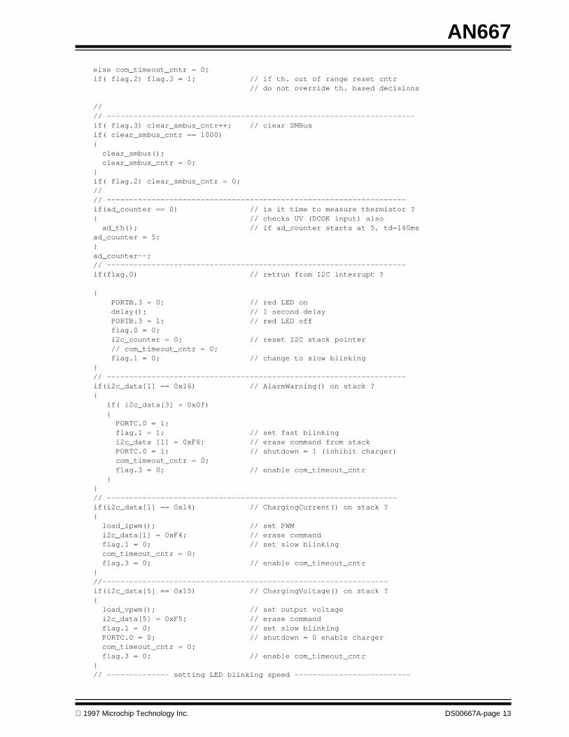
AN667
else com_timeout_cntr = 0; if( flag.2) flag.3 = 1; // if th. out of range reset cntr // do not override th. based decisions // // --------------------------------------------------------------------- if( flag.3) clear_smbus_cntr++; // clear SMBus if( clear_smbus_cntr == 1000) clear_smbus(); clear_smbus_cntr = 0; if( flag.2) clear_smbus_cntr = 0; // // ------------------------------------------------------------------- if(ad_counter == 0) // is it time to measure thermistor ? // checks UV (DCOK input) also ad_th(); // if ad_counter starts at 5, td=140ms ad_counter = 5; ad_counter--; // ------------------------------------------------------------------- if(flag.0) // retrun from I2C interrupt ? PORTB.3 = 0; // red LED on delay(); // 1 second delay PORTB.3 = 1; // red LED off flag.0 = 0; i2c_counter = 0; // reset I2C stack pointer // com_timeout_cntr = 0; flag.1 = 0; // change to slow blinking // ------------------------------------------------------------------- if(i2c_data[1] == 0x16) // AlarmWarning() on stack ? if( i2c_data[3] > 0x0f) PORTC.0 = 1; flag.1 = 1; // set fast blinking i2c_data [1] = 0xF6; // erase command from stack PORTC.0 = 1; // shutdown = 1 (inhibit charger) com_timeout_cntr = 0; flag.3 = 0; // enable com_timeout_cntr // ----------------------------------------------------------------- if(i2c_data[1] == 0x14) // ChargingCurrent() on stack ? load_ipwm(); // set PWM i2c_data[1] = 0xF4; // erase command flag.1 = 0; // set slow blinking com_timeout_cntr = 0; flag.3 = 0; // enable com_timeout_cntr //---------------------------------------------------------------- if(i2c_data[5] == 0x15) // ChargingVoltage() on stack ? load_vpwm(); // set output voltage i2c_data[5] = 0xF5; // erase command flag.1 = 0; // set slow blinking PORTC.0 = 0; // shutdown = 0 enable charger com_timeout_cntr = 0; flag.3 = 0; // enable com_timeout_cntr // -------------- setting LED blinking speed --------------------------
1997 Microchip Technology Inc. DS00667A-page 13

AN667
// if(flag.1) // fast blinking green requested ? // or shutdown LED_counter++; if(LED_counter > 1) // is it time to change status of LED ? LED_counter = 0; // if yes, clear counter if(PORTB.2) PORTB.2=0; // and toggle LED else PORTB.2 = 1; if(!flag.1) // slow flashing green - charging LED_counter++; if(LED_counter > 4) // time to change LED status ? LED_counter = 0; // if yes, reset counter if(PORTB.2) PORTB.2=0; // and toggle LED else PORTB.2 = 1; // end of while // end of main // ------------------------------------------------------------- //void clear_smbus( void ) TRISC.SDA = 1; // set as input TRISC.SCL = 1; // set as input // PORTC.SDA = 0; // to pull down SDA line when TRISC.SDA=L SSPCON.SSPEN = 0; // configure SDA and SCL pins as i/o pins // if( !PORTC.SCL) goto clsm1; // SMBus traffic ? jump if yes delay_5us(); if( !PORTC.SCL) goto clsm1; // SMBus traffic ? jump if yes delay_5us(); if( !PORTC.SCL) goto clsm1; // SMBus traffic ? jump if yes // TRISC.SDA = 0; // SDA -> ~~~\___ start delay_5us(); TRISC.SDA = 1; // SDA -> ___/~~~ stop // clsm1: PORTC.SDA = 1; TRISC.SDA = 1; // set as output TRISC.SCL = 1; // set as output SSPCON.SSPEN = 1; // cofigure SDA and SCL as serial port pins ////--------------------------------------------------------------// initialize voltage and current PWMs.//--------------------------------------------------------------void initiv( char a ) if( a==1) i2c_data[1] = 0x14; // ChargingCurrent command i2c_data[2] = 0x64; // charging current L byte i2c_data[3] = 0x00; // H byte i2c_data[5] = 0x15; // ChargingVoltage command i2c_data[6] = 0xFF; // charging voltage L byte i2c_data[7] = 0xFF; // H byte if( a==0)
DS00667A-page 14 1997 Microchip Technology Inc.
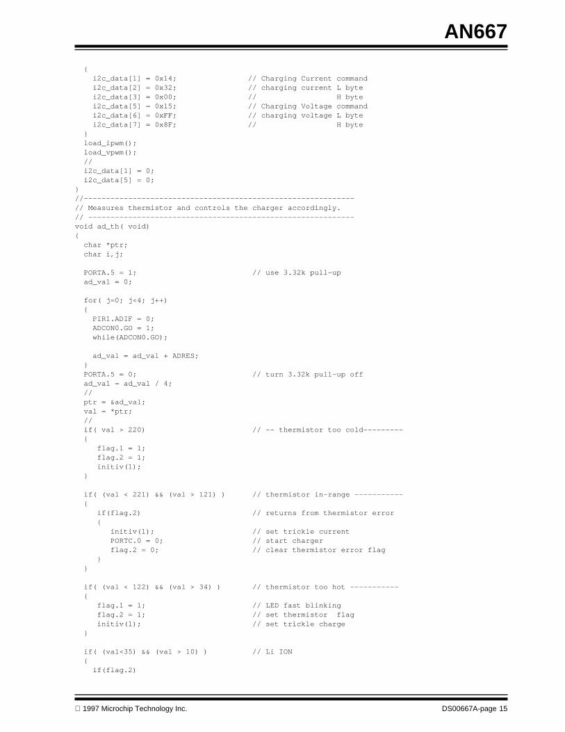
AN667
i2c_data[1] = 0x14; // Charging Current command i2c_data[2] = 0x32; // charging current L byte i2c_data[3] = 0x00; // H byte i2c_data[5] = 0x15; // Charging Voltage command i2c_data[6] = 0xFF; // charging voltage L byte i2c_data[7] = 0x8F; // H byte load_ipwm(); load_vpwm(); // i2c_data[1] = 0; i2c_data[5] = 0;//-------------------------------------------------------------// Measures thermistor and controls the charger accordingly.// ------------------------------------------------------------void ad_th( void) char *ptr; char i,j;
PORTA.5 = 1; // use 3.32k pull-up ad_val = 0;
for( j=0; j<4; j++) PIR1.ADIF = 0; ADCON0.GO = 1; while(ADCON0.GO);
ad_val = ad_val + ADRES; PORTA.5 = 0; // turn 3.32k pull-up off ad_val = ad_val / 4; // ptr = &ad_val; val = *ptr; // if( val > 220) // -- thermistor too cold--------- flag.1 = 1; flag.2 = 1; initiv(1);
if( (val < 221) && (val > 121) ) // thermistor in-range ----------- if(flag.2) // returns from thermistor error initiv(1); // set trickle current PORTC.0 = 0; // start charger flag.2 = 0; // clear thermistor error flag
if( (val < 122) && (val > 34) ) // thermistor too hot ----------- flag.1 = 1; // LED fast blinking flag.2 = 1; // set thermistor flag initiv(1); // set trickle charge
if( (val<35) && (val > 10) ) // Li ION if(flag.2)
1997 Microchip Technology Inc. DS00667A-page 15

AN667
initiv(0); PORTC.0 = 0; // start charger flag.2 = 0; // clear error flag if( val< 11) // Thermistor shorted flag.1 = 1; // green LED fast blinking flag.2 = 1; // set thermistor flag initiv(1); // set trickle charge //----------------------------------------------------------------// reads current values from i2c_dat[2] and i2c_data[3] locations,// (L and H bytes) limits the current, scales current word, and// loadx PWM registers (10 bit mode)//-----------------------------------------------------------------void load_ipwm( void ) long idata; char *ptr; bits ilowbits; // ptr = &idata; // get address of idata // *ptr = i2c_data[2]; // load L byte of idata *(ptr+1) = i2c_data[3]; // load H byte of idata // if(idata > 2600) idata = 2600; // idata >>=2; // scale idata 4096mA / 1024 = 4 ilowbits = *ptr; // save L byte // idata >>=2; // upper 8 bit of data // CCP2CON.CCP2X = ilowbits.1; // load lower two LSBits of 10 bit word to PWM CCP2CON.CCP2Y = ilowbits.0; CCPR2L = *ptr; // load upper 8 bit of 10 bit PWM word ////---------------------------------------------------------------------// Reads voltage data from i2c_data[6] (L byte) and i2c_data[7] locations,// assembles a 16 bit word. Limits the voltage at max 20V, scales vdata// voltage data word and loads PWM with 10 bit data.//------------------------------------------------------------------------void load_vpwm( void ) long unsigned vdata; char *ptr; bits vlowbits; // ptr = &vdata; // get address of idata *ptr = i2c_data[6]; // load L byte of idata *(ptr+1) = i2c_data[7]; // load H byte of idata // if(vdata < 8000) vdata = 8000; // PWM1 0x000 =8V, 0x3FF = 20V if(vdata > 18000) vdata=18000; // limit incoming voltage to 20V // vdata = vdata-6000; // // vdata >>= 4; // scale vdata 22-6=16V, 16V/1024=16 vlowbits = *ptr; // save L byte vdata >>=2; // upper 8 bit of data // CCP1CON.CCP1X = vlowbits.1; // load lower two LSBits of 10 bit word
DS00667A-page 16 1997 Microchip Technology Inc.

AN667
CCP1CON.CCP1Y = vlowbits.0; // to PWM 9-th and 10-th bits. CCPR1L = *ptr; // load upper 8 bit of 10 bit PWM word //------------------------------------------------------------------------void delay(void) char i, j, k; // software delay, about 1 sec for(k=0; k<2; k++) // measured: 840 msec. for(j=0; j<255; j++) for(i=0; i<255; i++); // inner loop delay: 1.647ms // ---------------------------------------------------------------------- void delay1( void ) char i,j; for(j=0; j<20; j++) for(i=0; i<155; i++); // delay 1ms // --------------------------------------------------------------------void delay_5us( void ) // 5us delay#asm nop nop nop nop#endasm //---------------------------------------------------------------------------void timer0( char a ) // td=(256-a)*256us @ 4MHz (prescaler /256) TMR0 = a; // reload load timer INTCON.T0IF = 0; // reset TMR0 interrupt flag//---------------------------------------------------------------------------//void init_var( void )//------INIT TMR0-------------- // OPTION = 0b11010111; // init timer 1, no pull-up at b (bit7=1) // bit7 Port B pull-up enable (1=disable) // INTEDG 1=INT on rising of RBO/INT // T0CS TMR0 ck source 0 = internal // T0SE TMR0 source edge 1=H->L on RA4 // bit3 PSA prescaler assign. 1=WDT, 0=TMR0 // PS2:PS0 prascaler div. rate 2,4,8,16..
//--- TMR2 and PWMs ----------// T2CON = 0x04; // init timer, bit2 turns it on // bit7 unimplemented // bit6:bit3 postscaler select 1,2,3..16 // bit2 TMR2ON 1=TMR2 on 0=TMR2 off // bit1:bit0 prescaler div. 1, 4 or 16// CCP1CON = 0b00001100; // init PWM1 // bit7 unimplemented // unimplemented // bit1 for 10 bit mode (0 for 8bit)
1997 Microchip Technology Inc. DS00667A-page 17

AN667
// bit0 for 10 bit mode (0 for 8bit) // bit3:0 mode select 11xx= PWM mode // CCP2CON = 0b00001100; // init PWM2 // --- init port A -- PORTA = 0; // 76543210 TRISA = 0b11011011; // RA5 3.32k OUT // RA4 header 4 IN // RA3 header 3 IN // RA2 33.2k OUT // RA1 UV IN // RA0 analog in IN// ----init A/D------ // 76543210 ADCON0 = 0b01000001; // Analog digital converter module // bit7 ADCS1 A/D clock select // ADCS0 01= fosc/8 -> tconv=16us // CHS2 channel selection // CHS1 // bit3 CHS0 000 -> RA0 // GO/DONE_ start conv/finished // unimplemented // ADON 1= a/d on 0=a/d off // 76543210 ADCON1 = 0b00000100; // b7:b3 not implemented // b2:b0 analog port pin config. // 100 RA0=analog RA1=analog // RA2=digital RA3=digital, Vref=VDD
// ----init port B---// PORTB = 12; // 76543210 TRISB = 0b11110011; // RB7 (pin 28) -> header 11 IN // RB6 (pin 27) -> header 10 IN // RB5 (pin 26) DCOK input IN // RB4 (pin 25) -> header 5 IN // RB3 red LED OUT // RB2 grn. LED OUT // RB1 (pin 22) -> header 9 IN // RBO (pin 21) -> header 8 IN// ----init.port C---
PORTC = 1; // 76543210 TRISC = 0b11011000; // init PORTC C.2 = CCP1 C.1 = CCP2 // RC7 (pin18) header 7 // RC6 (pin17) header 6 // RC5 (pin16) header 5 // RC4 (pin15) SDA I2C data -> input // RC3 (pin14) SCL I2C clock -> input // RC2 (pin13) CCP1 PWM1 pin, -> output // RC1 (pin12) CCP2 PWM2 pin, -> output // RC0 (pin11) shutdown -> output
// ------------------------- CCPR1L = 10; // pulse width1 CCPR2L = 10; // pulse width2 PR2 = 255; // period time 200-> 200us
//---setting-up I2C communication ---------- // 76543210 SSPCON = 0b00110110; // sync serial port control register // B7 WCOL=0 Write collision det. (SW reset)
DS00667A-page 18 1997 Microchip Technology Inc.

AN667
// SSPOV=0 receive collision det (SW reset) // SSPEN=1 enable ser port ( SCK SDO open D) // CKP = 1 0=enable clock // B2:B0 SSPM2:SSPM0=110 slave mode.// --- timer interrupts--- INTCON.T0IF = 1; // reset TMR0 int flag INTCON.T0IE = 0; // 1=enable TMR0 interrupt
PIE1.SSPIE = 1; // enable i2c interrupt PIR1.SSPIF = 0; // reset i2c interrupt flag // T1CON = 0x00; // init TMR1, internal ck, prescaler div=1
i2c_data[0] = 0; // clear address locations i2c_data[1] = 0; i2c_data[2] = 0; i2c_data[3] = 0; i2c_data[4] = 0; i2c_data[5] = 0; i2c_data[6] = 0; i2c_data[7] = 0; i2c_data[8] = 0; i2c_data[9] = 0;
1997 Microchip Technology Inc. DS00667A-page 19
2002 Microchip Technology Inc.
Information contained in this publication regarding deviceapplications and the like is intended through suggestion onlyand may be superseded by updates. It is your responsibility toensure that your application meets with your specifications.No representation or warranty is given and no liability isassumed by Microchip Technology Incorporated with respectto the accuracy or use of such information, or infringement ofpatents or other intellectual property rights arising from suchuse or otherwise. Use of Microchip’s products as critical com-ponents in life support systems is not authorized except withexpress written approval by Microchip. No licenses are con-veyed, implicitly or otherwise, under any intellectual propertyrights.
Trademarks
The Microchip name and logo, the Microchip logo, FilterLab,KEELOQ, microID, MPLAB, PIC, PICmicro, PICMASTER,PICSTART, PRO MATE, SEEVAL and The Embedded ControlSolutions Company are registered trademarks of Microchip Tech-nology Incorporated in the U.S.A. and other countries.
dsPIC, ECONOMONITOR, FanSense, FlexROM, fuzzyLAB,In-Circuit Serial Programming, ICSP, ICEPIC, microPort,Migratable Memory, MPASM, MPLIB, MPLINK, MPSIM,MXDEV, PICC, PICDEM, PICDEM.net, rfPIC, Select Modeand Total Endurance are trademarks of Microchip TechnologyIncorporated in the U.S.A.
Serialized Quick Turn Programming (SQTP) is a service markof Microchip Technology Incorporated in the U.S.A.
All other trademarks mentioned herein are property of theirrespective companies.
© 2002, Microchip Technology Incorporated, Printed in theU.S.A., All Rights Reserved.
Printed on recycled paper.
Microchip received QS-9000 quality system certification for its worldwide headquarters, design and wafer fabrication facilities in Chandler and Tempe, Arizona in July 1999. The Company’s quality system processes and procedures are QS-9000 compliant for its PICmicro® 8-bit MCUs, KEELOQ® code hopping devices, Serial EEPROMs and microperipheral products. In addition, Microchip’s quality system for the design and manufacture of development systems is ISO 9001 certified.
Note the following details of the code protection feature on PICmicro® MCUs.
• The PICmicro family meets the specifications contained in the Microchip Data Sheet.• Microchip believes that its family of PICmicro microcontrollers is one of the most secure products of its kind on the market today,
when used in the intended manner and under normal conditions.• There are dishonest and possibly illegal methods used to breach the code protection feature. All of these methods, to our knowl-
edge, require using the PICmicro microcontroller in a manner outside the operating specifications contained in the data sheet. The person doing so may be engaged in theft of intellectual property.
• Microchip is willing to work with the customer who is concerned about the integrity of their code.• Neither Microchip nor any other semiconductor manufacturer can guarantee the security of their code. Code protection does not
mean that we are guaranteeing the product as “unbreakable”.• Code protection is constantly evolving. We at Microchip are committed to continuously improving the code protection features of
our product.
If you have any further questions about this matter, please contact the local sales office nearest to you.
y Aust Stree
Fax: 6
y Coson O
. BeidaChina Fax:
y Coiaisonr, ower
inaFax: 8
y Coison Oe Plaz
a Fax:
y Co
l Plazad
Fax
y CoLiaisonzhen
hina Fax:
y HonMetro
g KonFax: 8
y Inc.
4)ey RoIndiaax: 9
LE
MAMERICASCorporate Office2355 West Chandler Blvd.Chandler, AZ 85224-6199Tel: 480-792-7200 Fax: 480-792-7277Technical Support: 480-792-7627Web Address: http://www.microchip.comRocky Mountain2355 West Chandler Blvd.Chandler, AZ 85224-6199Tel: 480-792-7966 Fax: 480-792-7456
Atlanta500 Sugar Mill Road, Suite 200BAtlanta, GA 30350Tel: 770-640-0034 Fax: 770-640-0307Boston2 Lan Drive, Suite 120Westford, MA 01886Tel: 978-692-3848 Fax: 978-692-3821Chicago333 Pierce Road, Suite 180Itasca, IL 60143Tel: 630-285-0071 Fax: 630-285-0075Dallas4570 Westgrove Drive, Suite 160Addison, TX 75001Tel: 972-818-7423 Fax: 972-818-2924DetroitTri-Atria Office Building 32255 Northwestern Highway, Suite 190Farmington Hills, MI 48334Tel: 248-538-2250 Fax: 248-538-2260Kokomo2767 S. Albright Road Kokomo, Indiana 46902Tel: 765-864-8360 Fax: 765-864-8387Los Angeles18201 Von Karman, Suite 1090Irvine, CA 92612Tel: 949-263-1888 Fax: 949-263-1338New York150 Motor Parkway, Suite 202Hauppauge, NY 11788Tel: 631-273-5305 Fax: 631-273-5335San JoseMicrochip Technology Inc.2107 North First Street, Suite 590San Jose, CA 95131Tel: 408-436-7950 Fax: 408-436-7955Toronto6285 Northam Drive, Suite 108Mississauga, Ontario L4V 1X5, CanadaTel: 905-673-0699 Fax: 905-673-6509
ASIA/PACIFICAustraliaMicrochip TechnologSuite 22, 41 RawsonEpping 2121, NSWAustraliaTel: 61-2-9868-6733 China - BeijingMicrochip TechnologCo., Ltd., Beijing LiaiUnit 915Bei Hai Wan Tai BldgNo. 6 ChaoyangmenBeijing, 100027, No. Tel: 86-10-85282100China - ChengduMicrochip TechnologCo., Ltd., Chengdu LRm. 2401, 24th FlooMing Xing Financial TNo. 88 TIDU StreetChengdu 610016, ChTel: 86-28-6766200 China - FuzhouMicrochip TechnologCo., Ltd., Fuzhou LiaUnit 28F, World TradNo. 71 Wusi RoadFuzhou 350001, ChinTel: 86-591-7503506China - ShanghaiMicrochip TechnologCo., Ltd.Room 701, Bldg. BFar East InternationaNo. 317 Xian Xia RoShanghai, 200051Tel: 86-21-6275-5700China - ShenzhenMicrochip TechnologCo., Ltd., Shenzhen Rm. 1315, 13/F, SheRenminnan LuShenzhen 518001, CTel: 86-755-2350361Hong KongMicrochip TechnologUnit 901-6, Tower 2, 223 Hing Fong RoadKwai Fong, N.T., HonTel: 852-2401-1200 IndiaMicrochip TechnologIndia Liaison OfficeDivyasree Chambers1 Floor, Wing A (A3/ANo. 11, O’ShaugnessBangalore, 560 025, Tel: 91-80-2290061 F
WORLDWIDE SA
ralia Pty Ltdt
1-2-9868-6755
nsulting (Shanghai)ffice
jie
86-10-85282104
nsulting (Shanghai) Office
6-28-6766599
nsulting (Shanghai)fficea
86-591-7503521
nsulting (Shanghai)
a
: 86-21-6275-5060
nsulting (Shanghai)n Office Kerry Centre,
86-755-2366086
gkong Ltd.plaza
g52-2401-3431
ad
1-80-2290062
JapanMicrochip Technology Japan K.K.Benex S-1 6F3-18-20, ShinyokohamaKohoku-Ku, Yokohama-shiKanagawa, 222-0033, JapanTel: 81-45-471- 6166 Fax: 81-45-471-6122KoreaMicrochip Technology Korea168-1, Youngbo Bldg. 3 FloorSamsung-Dong, Kangnam-KuSeoul, Korea 135-882Tel: 82-2-554-7200 Fax: 82-2-558-5934SingaporeMicrochip Technology Singapore Pte Ltd.200 Middle Road#07-02 Prime CentreSingapore, 188980Tel: 65-334-8870 Fax: 65-334-8850TaiwanMicrochip Technology Taiwan11F-3, No. 207Tung Hua North RoadTaipei, 105, TaiwanTel: 886-2-2717-7175 Fax: 886-2-2545-0139
EUROPEDenmarkMicrochip Technology Nordic ApSRegus Business CentreLautrup hoj 1-3Ballerup DK-2750 DenmarkTel: 45 4420 9895 Fax: 45 4420 9910FranceMicrochip Technology SARLParc d’Activite du Moulin de Massy43 Rue du Saule TrapuBatiment A - ler Etage91300 Massy, FranceTel: 33-1-69-53-63-20 Fax: 33-1-69-30-90-79GermanyMicrochip Technology GmbHGustav-Heinemann Ring 125D-81739 Munich, GermanyTel: 49-89-627-144 0 Fax: 49-89-627-144-44ItalyMicrochip Technology SRLCentro Direzionale Colleoni Palazzo Taurus 1 V. Le Colleoni 120041 Agrate BrianzaMilan, Italy Tel: 39-039-65791-1 Fax: 39-039-6899883United KingdomArizona Microchip Technology Ltd.505 Eskdale RoadWinnersh TriangleWokingham Berkshire, England RG41 5TUTel: 44 118 921 5869 Fax: 44-118 921-5820
01/18/02
S AND SERVICE
2002 Microchip Technology Inc.