small-signal performance and modeling of sub-50 nm …gtimp/images/smallsignalperformance.pdf ·...
TRANSCRIPT

Available online at www.sciencedirect.com
www.elsevier.com/locate/sse
Solid-State Electronics 52 (2008) 899–908
Small-signal performance and modeling of sub-50 nm nMOSFETswith fT above 460-GHz
V. Dimitrov a, J.B. Heng a, K. Timp a, O. Dimauro a, R. Chan a, M. Hafez a, J. Feng a,T. Sorsch b, W. Mansfield b, J. Miner b, A. Kornblit b, F. Klemens b, J. Bower b, R. Cirelli b,
E.J. Ferry b, A. Taylor b, M. Feng a, G. Timp a,*
a University of Illinois at Urbana-Champaign, Electrical and Computer Engineering, 3041 Beckman Institute,
405 N Mathews, Urbana, IL 61801, United Statesb New Jersey Nanotechnology Consortium, Murray Hill, NJ 07974, United States
Received 18 May 2007; received in revised form 13 January 2008; accepted 29 January 2008Available online 17 March 2008
The review of this paper was arranged by Prof. A. Zaslavsky
Abstract
We have fabricated and tested the performance of sub-50 nm gate nMOSFETs to assess their suitability for mixed signal applicationsin the super high frequency (SHF) band, i.e. 3–30 GHz. For a 30 nm � 40 lm � 2 device, we found fT = 465 GHz at Vds = 2 V,Vg = 0.67 V, which is the highest cut-off frequency reported for a MOSFET produced on bulk silicon substrate so far. However, ourmeasurements of fmax and noise figure indicate that parasitics impose limitations on SHF operation. We also present a high frequencyac model appropriate to sub-50 nm gate length nanotransistors, which incorporates the effects of the parasitics. The model accuratelyaccounts for measurements of the S- and Y-parameters in the frequency range from 1 to 50 GHz.� 2008 Elsevier Ltd. All rights reserved.
Keywords: Radio frequency (RF) MOSFET; RF MOSFET modeling; High frequency; Mixed signal
1. Introduction
Mobile, wireless communications are changing every-thing. Portable communication devices like the cell phone,along with 3 G, WLAN, and Bluetooth� are spurring thedemand for high frequency, mixed signal integrated circuitsthat are inexpensive, reliable and have a long battery life.CMOS technology can satisfy these demands. The relent-less scaling of CMOS toward nanometer-scale gate lengthshas produced MOSFETs with digital and RF performancethat is suitable for mixed signal applications.
The merit of a transistor depends on the circuit design.While large signal digital integrated circuits often use gate
0038-1101/$ - see front matter � 2008 Elsevier Ltd. All rights reserved.
doi:10.1016/j.sse.2008.01.025
* Corresponding author. Tel.: +1 2172449629; fax: +1 2172446622.E-mail address: [email protected] (G. Timp).
delay as a metric, the same loading conditions do not gen-erally apply to RF circuits [1]. Three figures-of-meritappropriate to small-signal RF performance are the cut-off frequency associated with the short-circuit current gain,
fT � gm=2pðCgs þ CgdÞ � 1=Lng ð1Þ
the maximum frequency of oscillation (where the unilateralpower gain vanishes),
fmax � fT=2ffiffiffiffiffiffiffiffiffiffiffiffiffiffiffiffiffiffiffiffiffiffiffiffiffiffiffiffiffiffiffiffiffiffiffiffiffiRgðgds þ 2pfTCgdÞ
q� 1=ðLn
gW Þ ð2Þ
and the noise figure Fmin,
F min � 1þ KfffiffiffiffiffiffiffiffiffiffiffiffiffiffiffiffiffiffiffiffiffiffiffiffigmðRg þ RsÞ
q=fT ð3Þ
where gm is the transconductance, Cgs and Cgd are thegate-to-source and gate-to-drain capacitances, Rs is the

900 V. Dimitrov et al. / Solid-State Electronics 52 (2008) 899–908
parasitic source resistance, Rg is the (lumped) gate resis-tance, gds is the output conductance, W is the total gatewidth, n is an index that ranges from 1 < n < 2 dependingon the transistor model (short or long channel), and K isa constant that depends on the technology. Ostensibly,improvements in fT follow from scaling of the gate length,Lg. There has been a progressive increase in fT to 330 GHzfor a 60 nm gate length nMOSFET [2–5], which is compa-rable to observations in sub-100 nm InP HEMTs [6], butstill inferior to reports on SiGe [7] and InP/InGaAs HBTs[8–10]. On the other hand, in MOS technology, fmax gener-ally lags behind fT – the disparity can be accounted for byparasitics, [2,11–13] such as Rg and gds that are not opti-mized in a core CMOS manufacturing process. Withacceptable gain, the noise figure, Fmin, also has to be min-imized to make effective use of CMOS technology for RF.Like fT, Fmin has been found to improve (diminish) witheach technology generation [2], but just like fmax, Fmin alsodepends on parasitic elements that are sensitive to the gatebias and geometry.
Along with the RF performance, another prerequisitefor the implementation of mixed circuits in CMOS is accu-rate, high frequency models for the MOSFET [13–24] andpassives. Specifically, the MOSFET model must accuratelyrepresent the power gain, input and output impedance andphase delay between the gate voltage and the drain current.A microwave table-based approach to modeling can bevery accurate, but requires a large database obtained fromnumerous measurements and computationally intensivesimulations – it becomes intractable for designing highlyintegrated CMOS communications circuits. Instead, acompact physics-based model is preferred, but a physics-based model has to be valid over a range of bias conditions,temperatures, and frequencies. Consequently, it has toaccount, not only for parasitic resistances and capaci-tances, but also for non-quasi-static (NQS) or distributedeffects in the gate, substrate and channel resistances dueto the channel propagation delay, and non-reciprocalcapacitances that account for the different effect of the gateand drain on each other in terms of charging currents[19,25].
Here, we report on the fabrication, testing and modelingof the RF performance of sub-50 nm gate length nMOS-FETs to assess their suitability for mixed signal applica-tions in the super high frequency (SHF) band, i.e. 3–30 GHz. Using a conventional process flow suitable for adigital technology, we fabricated nMOSFETs with gatelengths as short as 30 nm, and then we measured the DCand RF performance. Following Rashkin [26–28] weextended the usual de-embedding methodology [29] toaccount for additional access capacitances associated withmetal interconnections running between the (SOLT) refer-ence plane and the contacts to the drain, source and gate.With this refinement, we extracted an fT = 465 GHz frommeasurements of a 30 nm � 40 lm � 2(finger) nMOSFETtaken in the frequency range 1 GHz < f < 50 GHz atVds = 2 V, Vg = 0.67. This is the highest cut-off frequency
reported for a MOSFET so far. It represents a substantialimprovement over previous extrapolations using the sametransistors (fT = 290 GHz) that do not account for theaccess capacitance [30]. However, our measurements offmax 6 135 GHz and noise figure Fmin = 0.9 dB at 8 GHzindicate that parasitics still impose limitations on SHFoperation. The equivalent circuit that we developed tomodel the RF performance is based on Tsividis’s work[19] incorporating the effect of extrinsic and access parasi-tics and NQS. This model gives an accurate accountingof the measurements of the Y-parameters in the frequencyrange from 1 to 50 GHz and scales appropriately with thetransistor layout.
2. Fabrication
We have produced sub-50 nm nMOSFETs using aconventional process flow suitable for digital applications.The layout for the unit cell for each RF-MOSFET uses aco-planar waveguide structure to facilitate the RFmeasurements with a gate that is folded into a multi-leggedstructure and contacted from one side of the channel. Anexample of a two-legged MOSFET is shown in Fig. 1a.The aspect ratio of the folded gate guarantees that the totalgate resistance is determined by the length of the legs whilethe shared drain contact reduces the overall junction capac-itance. Using this geometry, we expect fmax to scale closelywith the length of the leg. An especially dramatic illustra-tion of the performance that can be recovered through gateengineering like this is the recent demonstration by Tiemei-jer et al. [12] of fmax = 150 GHz obtained using a 180 nmgate length CMOS foundry process that exhibits a cut-offfrequency of only fT = 70 GHz on a resistive 10 X-cmsubstrate.
A transmission electron micrograph of a cross-sectionthrough a representative MOSFET structure is shown inFig. 1b. The transistors were fabricated using 90 nm thickLOCOS isolation on float-zone (>800 X-cm) wafers. A30 keV boron implant with a fluence of 5.0E13 cm�2 wasused to form the p-tub, and a 7 keV boron implant at a flu-ence of 1.5 � 1013 cm�2 was used to form the channel. Sub-sequently, a 1.3 nm thick gate oxide was grown using rapidthermal oxidation, which was followed by the deposition ofa 95 nm thick in situ phosphorus-doped polysilicon layer.The 30–50 nm gate electrodes, defined by electron beamlithography in Sumitomo resist NEB31, were transferredinto the poly using reactive ion etching without using a hardmask. The gate-etch stopped on the thin gate oxide withouttrenching. Following the definition of polysilicon gates, anarsenic implant at 2.5 keV with fluence of 3.0 � 1014 cm�2
was used to form the shallow source/drain (S/D) extensions.Subsequently, a 30 nm silicon nitride layer was deposited ontop of a thin 10 nm silicon dioxide layer and subsequentlyetched to create the sidewall spacers. A 47 keV arsenicimplant at 4 � 1015 cm�2 was then used to define the S/D.The doping was activated using a rapid thermal annealfor 1 s at 1050 �C in nitrogen with a 75 �C/s ramp. Finally,

Fig. 1. (a) A scanning electron micrograph of a MOSFET tester (metal contacts to the source, gate, and drain shown here). The cross-section of theMOSFET (blue dashed line) is shown in (b). (b) A transmission electron micrograph of one finger of a nominally 30 nm gate length nMOSFET with a1.3 nm thick gate oxide. The gate is comprised of heavily doped polysilicon 95 nm thick with a CoSi2 strap. The 40 nm sidewalls consist of a 10 nm thickoxide beneath 30 nm of silicon nitride. A magnified view of the area outlined in red is shown in (c). The gate oxide appears to be about 1.3 nm thick. (Forinterpretation of the references in colour in this figure legend, the reader is referred to the web version of this article.)
V. Dimitrov et al. / Solid-State Electronics 52 (2008) 899–908 901
we used a cobalt-salicide process to lower the gate and S/Dresistance to about 8 X/sq. The salicide consisted of thedeposition of 5.0 nm of Cobalt followed by anneals for30 s at 550 �C and for 30 s at 750 �C for the formation ofa highly conductive CoSi2 layer.
The back end of the process used 400 nm of dielectric(TEOS) to isolate the 0.75 lm aluminum co-planar wave-guide structures (used for RF measurements) from thehigh-resistivity float-zone substrate. A 50 nm silicon nitridelayer prior to the TEOS deposition was used to facilitatethe etching of 0.5 lm vias by protecting the silicided gateand S/D extensions. After the vias to the S/D and the gatewere etched, a 30 nm Ti/80 nm TiN layer was depositedand annealed at 700 �C for 20 s prior to aluminum deposi-tion to serve as a diffusion barrier and aid the adhesion ofthe aluminum. Finally, before the metal contact lithogra-phy, 25 nm of TiN was deposited to cap the aluminum.
Fig. 2. The drain, transconductance, and subthreshold characteristicsmeasured in 45 nm � 20 lm � 2 (a–c) and 30 nm � 40 lm � 2 (d–f)nMOSFETs, respectively. The drive current ID = 1.8 mA/lm and1.9 mA/lm at Vds = Vg = 2 V for (a) and (d), respectively. The maximumtransconductance in the saturation region is gm = 0.94 mS/lm and 1.1 mS/lm at Vds = 2 V and Vg = 0.67 V for (b) and (e), respectively.
3. DC characteristics
We measured the dc current–voltage characteristics ofMOSFETs fabricated this way. Typical results obtainedfor a gate length 45 nm � 20 lm � 2 (gate length � gatewidth � number of fingers) and Lg = 30 nm � 40 lm � 2MOSFETs are shown respectively in Fig. 2a–c and d–f.For the 30 nm gate, we found a drive currentID = 1.9 mA/lm at Vds = VG = 2 V and an off-state cur-rent of 310 lA/lm, measured at VG = 0 V and Vds = 2 V,giving an Ion/Ioff = 6. The maximum transconductance inthe saturation region is gm = 0.94 mS/lm, which is foundat Vds = 2 V for VG = 0.67 V. For the 45 nm device, weobserve a drive current ID = 1.8 mA/lm at Vds = VG = 2 Vwith an off-state current of 55 lA/lm, giving an Ion/
Ioff = 33. The maximum transconductance in the saturationregion is gm = 1.1 mS/lm at Vds = 2 V and VG = 0.67 V.
From the subthreshold characteristic shown in Fig. 2cand f, we infer that short channel effects like drain inducedbarrier lowering and channel length modulation affect thedevice performance. In particular, the drain characteristicindicates a finite output resistance that can be represented
by a lumped element of 30 X in the intrinsic model forthe MOSFET see Table 1). The short channel effects areespecially evident in the 30 nm device, which result in areduced transconductance even though the gate length issmaller. Another detrimental factor may be the series resis-tance associated with the relatively thin (0.75 lm) alumi-num layer used for the coplanar waveguide structure.
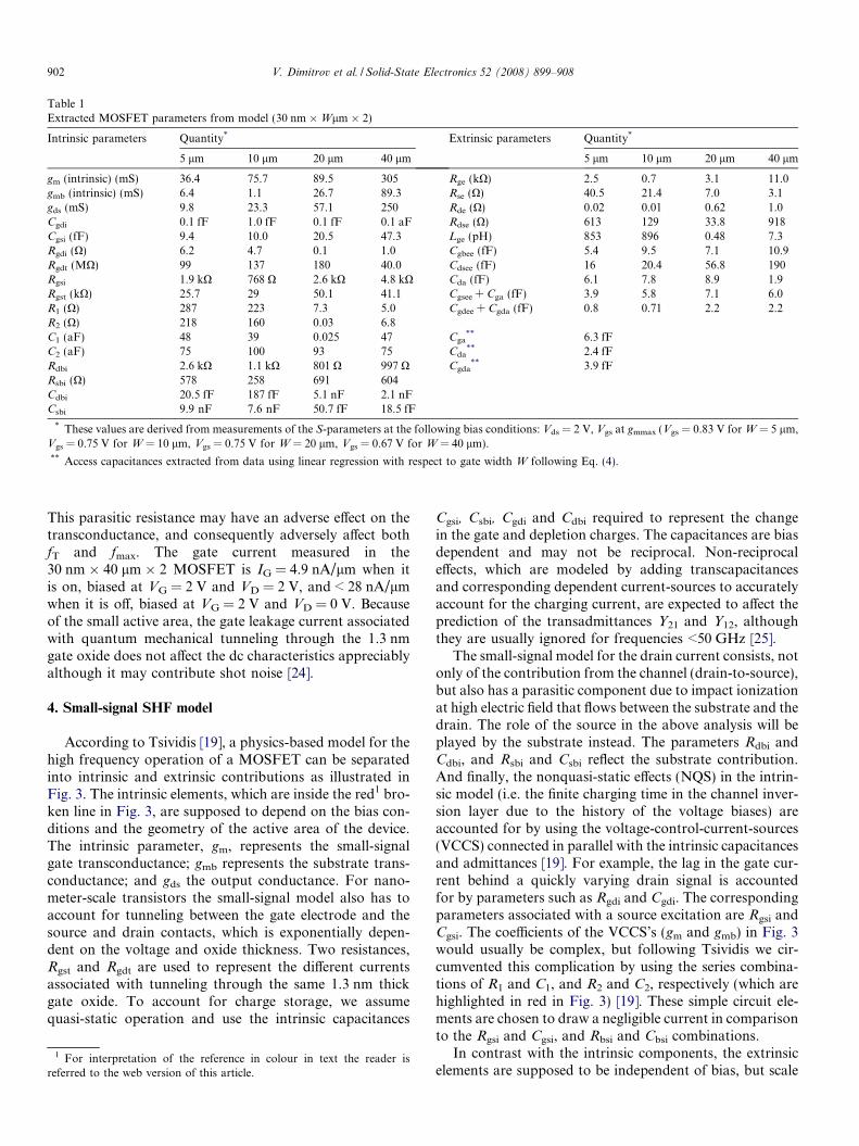
Table 1Extracted MOSFET parameters from model (30 nm �Wlm � 2)
Intrinsic parameters Quantity* Extrinsic parameters Quantity*
5 lm 10 lm 20 lm 40 lm 5 lm 10 lm 20 lm 40 lm
gm (intrinsic) (mS) 36.4 75.7 89.5 305 Rge (kX) 2.5 0.7 3.1 11.0gmb (intrinsic) (mS) 6.4 1.1 26.7 89.3 Rse (X) 40.5 21.4 7.0 3.1gds (mS) 9.8 23.3 57.1 250 Rde (X) 0.02 0.01 0.62 1.0Cgdi 0.1 fF 1.0 fF 0.1 fF 0.1 aF Rdse (X) 613 129 33.8 918Cgsi (fF) 9.4 10.0 20.5 47.3 Lge (pH) 853 896 0.48 7.3Rgdi (X) 6.2 4.7 0.1 1.0 Cgbee (fF) 5.4 9.5 7.1 10.9Rgdt (MX) 99 137 180 40.0 Cdsee (fF) 16 20.4 56.8 190Rgsi 1.9 kX 768 X 2.6 kX 4.8 kX Cda (fF) 6.1 7.8 8.9 1.9Rgst (kX) 25.7 29 50.1 41.1 Cgsee + Cga (fF) 3.9 5.8 7.1 6.0R1 (X) 287 223 7.3 5.0 Cgdee + Cgda (fF) 0.8 0.71 2.2 2.2R2 (X) 218 160 0.03 6.8C1 (aF) 48 39 0.025 47 Cga
** 6.3 fFC2 (aF) 75 100 93 75 Cda
** 2.4 fFRdbi 2.6 kX 1.1 kX 801 X 997 X Cgda
** 3.9 fFRsbi (X) 578 258 691 604Cdbi 20.5 fF 187 fF 5.1 nF 2.1 nFCsbi 9.9 nF 7.6 nF 50.7 fF 18.5 fF
* These values are derived from measurements of the S-parameters at the following bias conditions: Vds = 2 V, Vgs at gmmax (Vgs = 0.83 V for W = 5 lm,Vgs = 0.75 V for W = 10 lm, Vgs = 0.75 V for W = 20 lm, Vgs = 0.67 V for W = 40 lm).** Access capacitances extracted from data using linear regression with respect to gate width W following Eq. (4).
902 V. Dimitrov et al. / Solid-State Electronics 52 (2008) 899–908
This parasitic resistance may have an adverse effect on thetransconductance, and consequently adversely affect bothfT and fmax. The gate current measured in the30 nm � 40 lm � 2 MOSFET is IG = 4.9 nA/lm when itis on, biased at VG = 2 V and VD = 2 V, and < 28 nA/lmwhen it is off, biased at VG = 2 V and VD = 0 V. Becauseof the small active area, the gate leakage current associatedwith quantum mechanical tunneling through the 1.3 nmgate oxide does not affect the dc characteristics appreciablyalthough it may contribute shot noise [24].
4. Small-signal SHF model
According to Tsividis [19], a physics-based model for thehigh frequency operation of a MOSFET can be separatedinto intrinsic and extrinsic contributions as illustrated inFig. 3. The intrinsic elements, which are inside the red1 bro-ken line in Fig. 3, are supposed to depend on the bias con-ditions and the geometry of the active area of the device.The intrinsic parameter, gm, represents the small-signalgate transconductance; gmb represents the substrate trans-conductance; and gds the output conductance. For nano-meter-scale transistors the small-signal model also has toaccount for tunneling between the gate electrode and thesource and drain contacts, which is exponentially depen-dent on the voltage and oxide thickness. Two resistances,Rgst and Rgdt are used to represent the different currentsassociated with tunneling through the same 1.3 nm thickgate oxide. To account for charge storage, we assumequasi-static operation and use the intrinsic capacitances
1 For interpretation of the reference in colour in text the reader isreferred to the web version of this article.
Cgsi, Csbi, Cgdi and Cdbi required to represent the changein the gate and depletion charges. The capacitances are biasdependent and may not be reciprocal. Non-reciprocaleffects, which are modeled by adding transcapacitancesand corresponding dependent current-sources to accuratelyaccount for the charging current, are expected to affect theprediction of the transadmittances Y21 and Y12, althoughthey are usually ignored for frequencies <50 GHz [25].
The small-signal model for the drain current consists, notonly of the contribution from the channel (drain-to-source),but also has a parasitic component due to impact ionizationat high electric field that flows between the substrate and thedrain. The role of the source in the above analysis will beplayed by the substrate instead. The parameters Rdbi andCdbi, and Rsbi and Csbi reflect the substrate contribution.And finally, the nonquasi-static effects (NQS) in the intrin-sic model (i.e. the finite charging time in the channel inver-sion layer due to the history of the voltage biases) areaccounted for by using the voltage-control-current-sources(VCCS) connected in parallel with the intrinsic capacitancesand admittances [19]. For example, the lag in the gate cur-rent behind a quickly varying drain signal is accountedfor by parameters such as Rgdi and Cgdi. The correspondingparameters associated with a source excitation are Rgsi andCgsi. The coefficients of the VCCS’s (gm and gmb) in Fig. 3would usually be complex, but following Tsividis we cir-cumvented this complication by using the series combina-tions of R1 and C1, and R2 and C2, respectively (which arehighlighted in red in Fig. 3) [19]. These simple circuit ele-ments are chosen to draw a negligible current in comparisonto the Rgsi and Cgsi, and Rbsi and Cbsi combinations.
In contrast with the intrinsic components, the extrinsicelements are supposed to be independent of bias, but scale
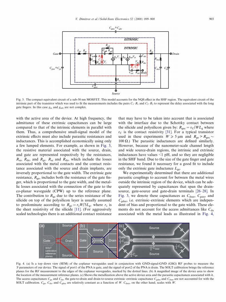
Fig. 3. The compact equivalent circuit of a sub-50 nm MOSFET. This model accounts for the NQS effect in the SHF region. The equivalent circuit of theintrinsic part of the transistor which was used to fit the measurements includes the pairs C1–R1 and C2–R2 to represent the delay associated with the longgate fingers. In this case gm and gmb are not complex.
V. Dimitrov et al. / Solid-State Electronics 52 (2008) 899–908 903
with the active area of the device. At high frequency, theadmittance of these extrinsic capacitances can be largecompared to that of the intrinsic elements in parallel withthem. Thus, a comprehensive small-signal model of theextrinsic effects must also include parasitic resistances andinductances. This is accomplished economically using onlya few lumped elements. For example, as shown in Fig. 3,the resistive material associated with the source, drain,and gate are represented respectively by the resistances,Rse, Rde, and Rge. Rse and Rde, which include the lossesassociated with the metal contacts and the contact resis-tance associated with the source and drain implants, areinversely proportional to the gate width. The extrinsic gateresistance, Rge, includes both the resistance of the gate fin-ger, which is proportional to the gate width, and the metal-lic losses associated with the connection of the gate to theco-planar waveguide (CPW) up to the reference plane.The contribution to Rge due to the series resistance of thesilicide on top of the polysilicon layer is usually assumedto predominate according to Rge = rsW/3Lg, where rs isthe sheet resistivity of the silicide [11]. (For aggressivelyscaled technologies there is an additional contact resistance
Fig. 4. (a) Is a top–down view (SEM) of the coplanar waveguides used inY-parameters of our device. The signal of port1 of the PNA is gate, and the signplanes for the RF measurement to the edges of the coplanar waveguides, marthe location of the measurement reference planes. (c) Shows the metallization abThe access capacitances Cga and Cda, the gate-to-drain and drain-to-source extSOLT calibration. Cga, Cda, and Cgdee are relatively constant as a function of
that may have to be taken into account that is associatedwith the interface due to the Schottky contact betweenthe silicide and polysilicon given by: Rgec = rC/WLg whererC is the contact resistivity [31]. For a typical transistorused in these experiments W P 5 lm and Rge > Rgec �100 X.) The parasitic inductances are defined similarly.However, because of the nanometer-scale channel lengthand wide source-drain regions, the intrinsic and extrinsicinductances have values <1 pH, and so they are negligiblein the SHF band. Due to the size of the gate finger and gateresistance, we found it necessary for a good fit to includeonly the extrinsic gate inductance Lge.
We experimentally determined that there are additionalparasitic couplings to account for between the metal wiresoutside the intrinsic region of the device, which can be ade-quately represented by capacitances that span the drain-source, gate-source and gate-drain terminals [26–28]. InFig. 3, we denote these capacitances as Cdsee, Cgsee, andCgdee, i.e. extrinsic–extrinsic elements which are indepen-dent of bias and proportional to the gate width. These ele-ments do not account for the access admittances like Cda
associated with the metal leads as illustrated in Fig. 4,
conjunction with GND-signal-GND (GSG) RF probes to measure theal of port2 of the PNA is drain. The SOLT calibration brings the reference
ked by the dotted lines. (b) A magnified image of the device area to showove the active device area and the parasitic capacitances associated with it.rinsic–extrinsic capacitance Cgdee and Cdsee are not accounted for with theW. Cdsee, on the other hand, scales with W.

904 V. Dimitrov et al. / Solid-State Electronics 52 (2008) 899–908
however. Although the access admittances can be ade-quately represented by capacitances in parallel with theseextrinsic–extrinsic capacitances, they scale differently. So,Fig. 3 indicates that the access capacitances Cga and Cgda
are summed with the corresponding extrinsic–extrinsiccapacitances.
Fig. 5. Comparison of the Y-parameters of the model and measured datafor a 30 nm � 40 lm � 2 device from 1 GHz to 50 GHz. Both the real(gray lines) and imaginary (black lines) parts of the model are comparedwith the real (grey triangles) and imaginary (black triangles) parts of themeasured Y-parameters respectively. We find excellent agreement betweenthe model and measurements in the 3–30 GHz band.
5. Measurements of the small-signal SHF performance
The RF performance from 50 MHz to 50 GHz of nano-transistors embedded in a CPW was measured using anAgilent E8364B PNA. To launch the signal from the RFprobe tips to the device under test (DUT), a CPW is usedin a ground-signal-ground configuration as shown in themicrograph of Fig. 4. Because of the relative size of thedevice, parasitic elements associated with the contact padsand interconnects cannot be neglected. So, the intrinsic per-formance of the transistor had to be de-embedded from thedata.
We used Y-parameters to characterize the RF measure-ments. To obtain an accurate assessment of the Y-parame-ters, we used a two step procedure. First, using a full 2-portSOLT calibration [26,29], we automatically subtracted theY-parameters associated with on-wafer standards consist-ing of a short, an open, a load (nominally 50 X, and a thru(SOLT) from the DUT measurements using the E8364B.(This extends the reference plane to the dotted line inFig. 4b.) While this calibration technique is renowned forits accuracy [29], it does not account for the access admit-tances like Cda indicated in Fig. 4c associated with themetal leads extending from the SOLT reference plane andto the source, drain and gate contacts. Since the MOSFETgate width does not extend into the ground plane of theCPW, (see Fig. 4b), the access admittances can be ade-quately represented solely by capacitors.
The second step involves subtracting the admittanceassociated with the access capacitances from the imaginarypart of the SOLT calibrated measurements of the Y-param-eters. The access capacitances were inferred using a linearregression to determine the intercepts of the effective capac-itance (Im[Y/x]) versus gate width from measurements ofthe Y-parameters using extraction techniques based onthe ColdFET and Inversion approximations [25,28],with the MOSFET biased OFF, (i.e. Vds = 0 V and Vg <Vt), the active area of the device can be neglected, andthe imaginary part of the measured Y-parameters is thesum of the extrinsic capacitances and the access capaci-tances, i.e.
Im½Y 11� ffi xðCga þ Cgda þ Cgdee þ CgseeÞ ð4aÞIm½Y 12� ffi �xðCgda þ CgdeeÞ ð4bÞIm½Y 22� ffi xðCda þ Cgda þ Cgdee þ CdseeÞ ð4cÞ
Eqs. 4(a–c) are insufficient for discriminating betweenthe access capacitances and the extrinsic (or intrinsic)capacitances. However, the extrinsic and extrinsic–extrinsiccapacitances like Cdsee are directly proportional to the gate
width, while the access capacitances are independent of W.Thus, by using the intercepts of a regression line throughthe effective capacitance Im(Y/x) versus gate width, wecan determine the access capacitances. Two deficienciesof this method are: (1) the capacitances obtained includeother capacitances such as the gate-to-source capacitancedue to the enlarged region of the polysilicon used for con-tact access that is located on top of the LOCOS isolationoxide (usually negligible); and (2) there is additional errorintroduced by the regression equation.
Using Agilent’s Advanced Design System software to fitthe model to the data, we arrived at the final estimates forthe lumped elements represented in Fig. 3. For example, weextracted the intrinsic and extrinsic parameters associatedwith 30 nm �Wlm � 2 and 45 nm �Wlm � 2 MOS-FETs biased at Vds = 2.0 V and Vg at the maximum ofthe transconductance. Table 1 lists the values for all param-eters in the compact model of the 30 nm �Wlm � 2nMOSFET. These parameters are consistent with analyti-cal estimates given by Tsvidis [19]. For example, from[19] we expect Cgsi � (2/3)Cox and Cgdi � 0 and RgsiCgsi >
RgdiCgdi, despite the observation that the fit is insensitiveto the value of Rgdi. We find that without varying Rgsi,there is <1–2% change in the parameters and <50% changein the residual for 1 X < Rgdi < 2Rgsi.
Comparisons between the predictions of the model forthe 30 nm � 40 lm � 2 and 45 nm � 10 lm � 2 MOSFETsusing the parameters obtained from the extraction tech-nique and the measurements are illustrated in Figs. 5 and6, respectively. Generally, we find very close correspon-dence between the Y-parameters calculated from the modeland the measured data up to 50 GHz. Measurements ofboth the real and imaginary parts of the Y-parameters fol-

Fig. 6. Comparison of the Y-parameters of the model and measured datafor a 45 nm � 10 lm � 2 device from 1 GHz to 50 GHz. Both the real(gray lines) and imaginary (black lines) parts of the model are comparedwith the real (grey triangles) and imaginary (black triangles) parts of themeasured Y-parameters, respectively. We find excellent agreementbetween the model and measurements in the 3–30 GHz band.
V. Dimitrov et al. / Solid-State Electronics 52 (2008) 899–908 905
low the predictions of the model shown in Fig. 3, eventhough nonreciprocal transcapacitances (such as Cgdi andCdgi) are not included in the model, which was expectedto make it difficult to accurately predict Im[Y21] andIm[Y12] at the same time [25]. Unlike the measurementsobtained on 5, 10, and 20 lm channel width MOSFETs,neither Im[Y21] nor Im[Y22] approach zero in the frequencyrange shown in Figs. 5 and 6, which the model of Fig. 3attributes to the high gate resistance associated with the40 lm channel widths.
One advantage of this model of Fig. 3 is economy. Itcontains fewer parameters than the distributed version[30], and yet it still accurately accounts for the measure-ments in the frequency range from 1 GHz to 50 GHz,and scales appropriately with geometry. While this modelis compact, which facilitates IC design, the fit to the datadeteriorates slightly compared to the distributed model[30]. The error function v2, which is based on the sum ofthe squares of the residuals, is doubled from approximately0.03 to 0.05. This slight degradation of the fit, however, isimperceptible in the plots of the Y- parameters, the powergain and the current gain.
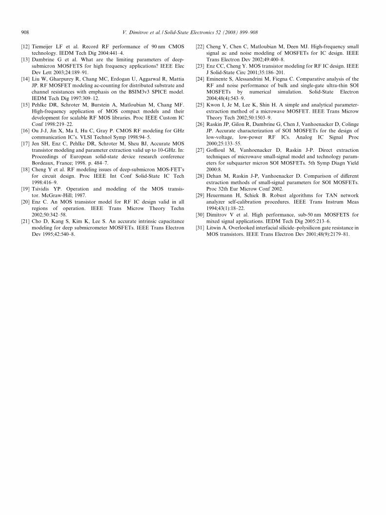
The extracted parameters match the results obtainedfrom low frequency or dc measurements and closely corre-spond to parameters estimated from the physical structureof the MOSFET. Fig. 7a and b compare low frequency (dc)measurements of the effective gm, and gds, with the intrinsicparameters extracted from the model of Fig. 3 in the lowfrequency limit (5 MHz). We find that the low frequencymeasurements generally correspond with the extractedparameters, except for a gate width of W = 40 lm wherethe model predicts larger values, beyond the error attrib-uted to the fit. The discrepancies found for a gate widthof W = 40 lm may be associated with the inability of the
lumped element model to capture the distributed natureof the gate, source, drain and channel resistances. It isnot observed for a distributed model for the gate [30]. Acomparison of measurements of the intrinsic capacitanceCgsi and the extrinsic parameter Cdsee versus gate widthare shown in Fig. 7c and d. To compare with the valuesextracted from the model (Fig. 3), we have estimated Cgsi
from PADRE simulations of the transistor geometry. Cgsee
was inferred from the measured Y-parameters using extrac-tion techniques based on the ColdFET approximation [25].
6. Figures-of-merit for RF-MOSFET amplifier
Fig. 8a illustrates the RF performance of 30 nm �40 lm � 2 nMOSFETs biased at the transconductancemaximum gm = 0.94 S/mm found at Vg = 0.67 V forVds = 2 V. The performance is indicated by the short-cir-cuit current gain, h21, and Mason’s unilateral gain, U. Bothh21, and U exhibit a nearly ideal single-pole response withfrequency, and so we infer fT and fmax by extrapolatingto unity gain at �20 dB/decade from data in the range40–50 GHz. For the 30 nm gate length MOSFET we findfT =465 GHz as indicated in Fig. 8a. However, a similarextrapolation using a single-pole response for data in therange 1–30 GHz indicates that fT ffi 500 GHz for the sameMOSFET as shown in Fig. 8b. This discrepancy from thesingle-pole response observed above 30 GHz is an indica-tion of the difficulty realizing adequate calibration at thehigh frequency end of the PNA.
An nMOSFET fT = 465 GHz is comparable to the bestSiGe-BJT reported in literature so far [6]. On the otherhand, the power gain performance measured byfmax = 45 GHz as shown in Fig. 8c is reduced by a factorof 10 from the cut-off frequency. The degradation of fmax
is an indication of the detrimental effect of parasitics indi-cated by Eq. (2). Relying on the agreement between themodel of Fig. 3 and measured current and power gainshown in Fig. 8c, we infer that parasitic elements such asthe gate resistance, Rge, and the series source and drainresistances, Rse and Rde, adversely affect the power gainin the SHF band. Moreover, previous extrapolations basedon the same measurements showed that fT = 290 GHz andfmax = 45 GHz for the 30 nm gate length [30]. The priorextrapolations reflect the detrimental effects of the accesscapacitances on the estimate of fT.
Figs. 9a and b illustrate measurements of the RF perfor-mance in the same 30 nm � 40 lm � 2 and 45 nm �20 lm � 2 nMOSFETs of Fig. 2, showing the same trendin current and power gain. There is an improvementgleaned in the current gain from decreasing the channellength: i.e. the 45 nm device shows fT = 350 GHz whilethe 30 nm MOSFET has an fT above 460 GHz. Fig. 9csummarizes the measured dependence of fT on the gatelength inferred from top–down scanning electron micros-copy (SEM) for devices with the same gate width. Withinthe error, we find that fT data is consistent with a 1/Lg
dependence associated with short channel MOSFETs over
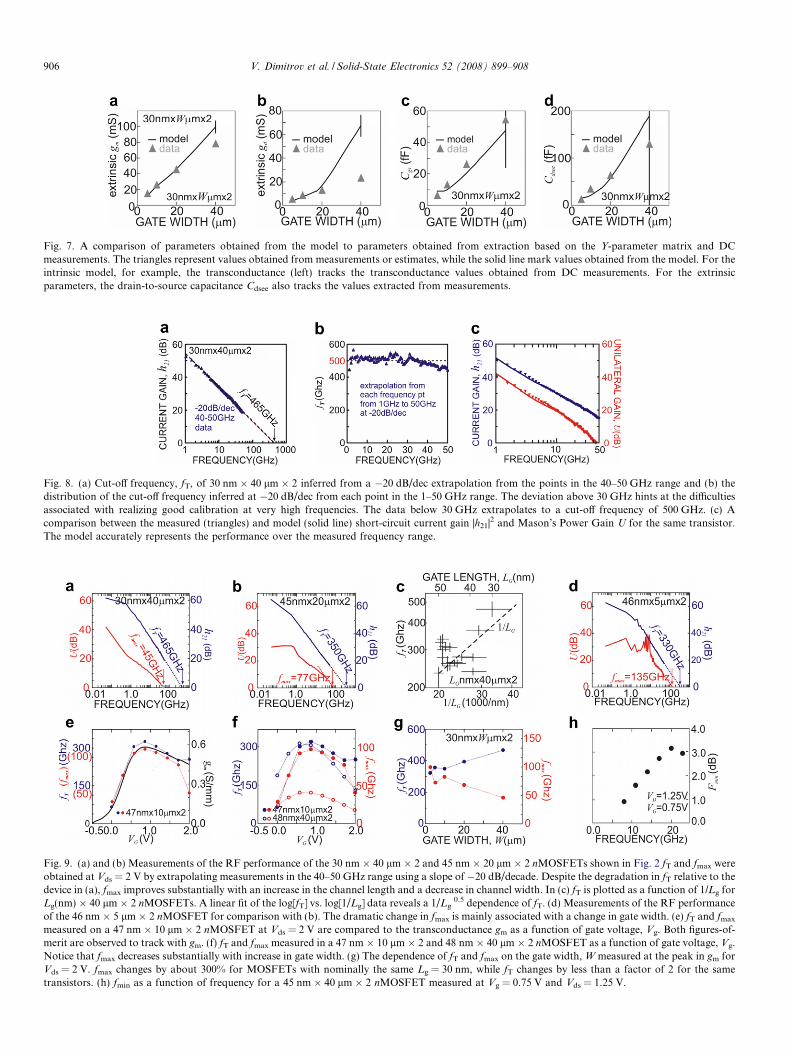
Fig. 7. A comparison of parameters obtained from the model to parameters obtained from extraction based on the Y-parameter matrix and DCmeasurements. The triangles represent values obtained from measurements or estimates, while the solid line mark values obtained from the model. For theintrinsic model, for example, the transconductance (left) tracks the transconductance values obtained from DC measurements. For the extrinsicparameters, the drain-to-source capacitance Cdsee also tracks the values extracted from measurements.
Fig. 8. (a) Cut-off frequency, fT, of 30 nm � 40 lm � 2 inferred from a �20 dB/dec extrapolation from the points in the 40–50 GHz range and (b) thedistribution of the cut-off frequency inferred at �20 dB/dec from each point in the 1–50 GHz range. The deviation above 30 GHz hints at the difficultiesassociated with realizing good calibration at very high frequencies. The data below 30 GHz extrapolates to a cut-off frequency of 500 GHz. (c) Acomparison between the measured (triangles) and model (solid line) short-circuit current gain |h21|2 and Mason’s Power Gain U for the same transistor.The model accurately represents the performance over the measured frequency range.
Fig. 9. (a) and (b) Measurements of the RF performance of the 30 nm � 40 lm � 2 and 45 nm � 20 lm � 2 nMOSFETs shown in Fig. 2 fT and fmax wereobtained at Vds = 2 V by extrapolating measurements in the 40–50 GHz range using a slope of �20 dB/decade. Despite the degradation in fT relative to thedevice in (a), fmax improves substantially with an increase in the channel length and a decrease in channel width. In (c) fT is plotted as a function of 1/Lg forLg(nm) � 40 lm � 2 nMOSFETs. A linear fit of the log[fT] vs. log[1/Lg] data reveals a 1/Lg
0.5 dependence of fT. (d) Measurements of the RF performanceof the 46 nm � 5 lm � 2 nMOSFET for comparison with (b). The dramatic change in fmax is mainly associated with a change in gate width. (e) fT and fmax
measured on a 47 nm � 10 lm � 2 nMOSFET at Vds = 2 V are compared to the transconductance gm as a function of gate voltage, Vg. Both figures-of-merit are observed to track with gm. (f) fT and fmax measured in a 47 nm � 10 lm � 2 and 48 nm � 40 lm � 2 nMOSFET as a function of gate voltage, Vg.Notice that fmax decreases substantially with increase in gate width. (g) The dependence of fT and fmax on the gate width, W measured at the peak in gm forVds = 2 V. fmax changes by about 300% for MOSFETs with nominally the same Lg = 30 nm, while fT changes by less than a factor of 2 for the sametransistors. (h) fmin as a function of frequency for a 45 nm � 40 lm � 2 nMOSFET measured at Vg = 0.75 V and Vds = 1.25 V.
906 V. Dimitrov et al. / Solid-State Electronics 52 (2008) 899–908

V. Dimitrov et al. / Solid-State Electronics 52 (2008) 899–908 907
the narrow range examined (30–50 nm) as anticipated fromEq. (1). The SEM measurements were found to be consis-tent with cross-sectional TEM assessments done on thesame devices using focused ion beam milling to preparethe specimens. The error associated with the length mea-surement develops from variations in the gate length alongthe width of the device associated with the lithography andetching. The error associated with the estimate of fT devel-ops mainly from errors in the measurement of the gain inthe 40–50 GHz band.
Both gds and Rge increase as the gate length decreases,which has a detrimental effect on fmax. So, we anticipate thatfmax � 1/W as indicated in Eq. (2), provided that gm, Rge, gds,Cgsi and Cgdi scale linearly with the gate width [11]. Figs. 9band d show two nMOSFETs of comparable gate length, butdifferent gate widths: i.e. 45 nm � 20 lm � 2 and46 nm � 5 lm � 2, respectively. As illustrated by a compar-ison of the two figures, devices with a shorter gate width deli-ver higher fmax without compromising fT. The 46 nm �5 lm � 2 device of Fig. 9d exhibits an fT = 330 GHz andfmax = 135 GHz, while the 45 nm � 20 lm � 2 device hasfT = 350 GHz and fmax = 77 GHz. Devices with a larger gatelength can potentially deliver higher fmax despite a reductionin fT since improvements in Rge and gds could compensate forthe degradation. The slight degradation of fT measured inthe device of Fig. 9d is offset by a decrease in W, Rg, and Rds.
We methodically explored the dependence of fT and fmax
on gate voltage, width and length. The measured gate volt-age-bias dependence of fT and fmax is illustrated in Fig. 9efor a 47 nm � 10 lm � 2 MOSFET. The observed depen-dence follows from the gate voltage dependence of thetransconductance as indicated in Eqs. (1) and (2). Gener-ally, for the devices we measured, both fT and fmax scalewith gm in the range 0 < Vg < 1.7 V. The measured depen-dence of fT and fmax on gate width is illustrated in Fig. 9ffor similar gate length nMOSFETs (47 nm versus 48 nm)with different gate widths (10 lm versus 40 lm, respec-tively). Notice that even though the peak values offT � 300 GHz are nearly identical, the peak value of fmax
for the 47 nm � 10 lm � 2 MOSFET is about 100 GHz,while the peak value for the 48 nm � 40 lm � 2 is less thanhalf that value, fmax = 41 GHz. Fig. 9g summarizes thetrends observed in fT and fmax as a function of the gatewidth for nominally 30 nm gate length MOSFETs. fT
increases as the gate width increases while fmax increaseswith decreasing W. The increase in fT with gate width Wis due to both proximity corrections in the electron beamlithography and gate etch that generate a narrower gatelength for larger gate widths.
Finally, to make effective use of CMOS technology forRF applications, the noise figure, Fmin, also has to be min-imized with an acceptable associated gain. So, we examinedthe broadband noise performance in the SHF band. Fig. 9hshows a linear frequency dependence of Fmin that we antic-ipated in Eq. (3). Fmin is about 0.9 dB at 8 GHz. Generally,we find a larger noise figure with increasing frequency –approaching 3 dB for frequencies above 20 GHz, which
compares favorably to data reported on 80 nm nMOSFETat the same operating point [2]. According to Eq. (3), weexpect an improvement in the noise figure if the gate resis-tance improves. For this 47 nm � 10 lm � 2 nMOSFET at8 GHz we find a maximum available gain of 22 dB withFmin < 1 dB, while at 20 GHz, we find a maximum avail-able gain of 11 dB with Fmin < 3.5 dB.
7. Conclusion
In summary, measurements of sub-50 nm gate nMOS-FETs reveal the highest RF performance of an nMOSFETso far. For a 30 nm � 40 lm � 2 device, we found fT >460 GHz at Vds = 2 V, Vg = 0.67 V after accounting foraccess capacitances. However, measurements of fmax 6
135 GHz and the noise figure indicate that parasiticsadversely affect the circuit performance. Very accuratemodels of the measurements in the SHF band that accountfor non-quasi-static effects and incorporate parasitic ele-ments indicate that the gate resistance and the source-drainlimit the power gain.
Acknowledgments
We gratefully acknowledge support from the Air Force(FA9550-04-1-0214), NSF (CCR 01-21616) and ONR(N00014-03-0268). The Center for Microanalysis of Mate-rials, supported by the DOE (DEFG02-91-ER45439), wasinstrumental in this work.
References
[1] Taylor GW, Simmons JG. Figure of merit for integrated bipolartransistors. Sol State Electron 1986;29:941–6.
[2] Kuhn K et al. A comparison of state-of-the-art NMOS and HBTdevices for analog/mixed-circuit/RF circuit application. VLSI TechSymp Tech Dig 2004;224.
[3] Momose HS, Ohguro T, Morifuji E, Sugaya H, Nakamura S, Iwai H.Cutoff frequency and propagation delay time of 1.5-nm gate oxideCMOS. IEEE Trans Electron Dev 2001;48:1165–74.
[4] Zamdmer N et al. A 243-GHz ft and 208-GHz fmax, 90-nm SOICMOS SoC technology with low-power millimeter-wave digital andRF circuit capability. VLSI Tech Symp 2004:98–9.
[5] Lee S, Wagner L, Janannathan B, Csutak S, Pekarik J, Zamdmer N,et al. Record RF performance of sub-46 nm Lgate NFETs inmicroprocessor SOI CMOS technologies. IEDM Tech Dig2005:241–4.
[6] Suemitsu T, Enoki T, Yokoyama H, Ishii Y. Impact of two-step-recessed gate structure on RF performance of InP-based HEMTs.Electron Lett 1998;34:220–2.
[7] Khater M et al. SiGe HBT technology with fmax/fT = 350/300 GHzand gate delay below 3.3 ps. IEDM Tech Dig 2004:247–50.
[8] Hafez W, Feng M. 0.25 lm emitter InP SHBTs with fT = 550 GHzand BVCEO > 2 V. IEDM Tech Dig 2004:549–52.
[9] Hussian T et al. First demonstration of sub-0.25 lm-width emitterInP-DHBTs with >400 GHz ft and >400 GHz fmax. IEDM Tech Dig2004:553–6.
[10] Yu D et al. Ultra high-speed 0.25-lm emitter InP-InGaAs SHBTswith fmax of 687 GHz. IEDM Tech Dig 2004:557–60.
[11] Razavi B, Yan R, Lee KF. Impact of distributed gate resistance onthe performance of MOS devices. IEEE Trans Circuit Syst-I1994;41:750–4.
908 V. Dimitrov et al. / Solid-State Electronics 52 (2008) 899–908
[12] Tiemeijer LF et al. Record RF performance of 90 nm CMOStechnology. IEDM Tech Dig 2004:441–4.
[13] Dambrine G et al. What are the limiting parameters of deep-submicron MOSFETS for high frequency applications? IEEE ElecDev Lett 2003;24:189–91.
[14] Liu W, Gharpurey R, Chang MC, Erdogan U, Aggarwal R, MattiaJP. RF MOSFET modeling ac-counting for distributed substrate andchannel resistances with emphasis on the BSIM3v3 SPICE model.IEDM Tech Dig 1997:309–12.
[15] Pehlke DR, Schroter M, Burstein A, Matloubian M, Chang MF.High-frequency application of MOS compact models and theirdevelopment for scalable RF MOS libraries. Proc IEEE Custom ICConf 1998:219–22.
[16] Ou J-J, Jin X, Ma I, Hu C, Gray P. CMOS RF modeling for GHzcommunication IC’s. VLSI Technol Symp 1998:94–5.
[17] Jen SH, Enz C, Pehlke DR, Schroter M, Sheu BJ, Accurate MOStransistor modeling and parameter extraction valid up to 10-GHz. In:Proceedings of European solid-state device research conferenceBordeaux, France; 1998. p. 484–7.
[18] Cheng Y et al. RF modeling issues of deep-submicron MOS-FET’sfor circuit design. Proc IEEE Int Conf Solid-State IC Tech1998:416–9.
[19] Tsividis YP. Operation and modeling of the MOS transis-tor. McGraw-Hill; 1987.
[20] Enz C. An MOS transistor model for RF IC design valid in allregions of operation. IEEE Trans Microw Theory Techn2002;50:342–58.
[21] Cho D, Kang S, Kim K, Lee S. An accurate intrinsic capacitancemodeling for deep submicrometer MOSFETs. IEEE Trans ElectronDev 1995;42:540–8.
[22] Cheng Y, Chen C, Matloubian M, Deen MJ. High-frequency smallsignal ac and noise modeling of MOSFETs for IC design. IEEETrans Electron Dev 2002;49:400–8.
[23] Enz CC, Cheng Y. MOS transistor modeling for RF IC design. IEEEJ Solid-State Circ 2001;35:186–201.
[24] Eminente S, Alessandrini M, Fiegna C. Comparative analysis of theRF and noise performance of bulk and single-gate ultra-thin SOIMOSFETs by numerical simulation. Solid-State Electron2004;48(4):543–9.
[25] Kwon I, Je M, Lee K, Shin H. A simple and analytical parameter-extraction method of a microwave MOSFET. IEEE Trans MicrowTheory Tech 2002;50:1503–9.
[26] Raskin JP, Gilon R, Dambrine G, Chen J, Vanhoenacker D, ColingeJP. Accurate characterization of SOI MOSFETs for the design oflow-voltage, low-power RF ICs. Analog IC Signal Proc2000;25:133–55.
[27] Goffioul M, Vanhoenacker D, Raskin J-P. Direct extractiontechniques of microwave small-signal model and technology param-eters for subquarter micron SOI MOSFETs. 5th Symp Diagn Yield2000:8.
[28] Dehan M, Raskin J-P, Vanhoenacker D. Comparison of differentextraction methods of small-signal parameters for SOI MOSFETs.Proc 32th Eur Microw Conf 2002.
[29] Heuermann H, Schiek B. Robust algorithms for TAN networkanalyzer self-calibration procedures. IEEE Trans Instrum Meas1994;43(1):18–22.
[30] Dimitrov V et al. High performance, sub-50 nm MOSFETS formixed signal applications. IEDM Tech Dig 2005:213–6.
[31] Litwin A. Overlooked interfacial silicide–polysilicon gate resistance inMOS transistors. IEEE Trans Electron Dev 2001;48(9):2179–81.