slvsdv6a –november 2017–revised …€¢ mobile computing, networking cards • solid state...
TRANSCRIPT

Copyright © 2017, Texas Instruments Incorporated
VIN
EN
PG
AGND
SW
FB
PGND
VOUT/2A2.4 to 5.5V
10µF
470nH
4.7µF R1
R2
VFB=0.6V
±1%
TPS62822Cff*
* optional
Product
Folder
Order
Now
Technical
Documents
Tools &
Software
Support &Community
An IMPORTANT NOTICE at the end of this data sheet addresses availability, warranty, changes, use in safety-critical applications,intellectual property matters and other important disclaimers. PRODUCTION DATA.
TPS62821, TPS62822, TPS62823SLVSDV6B –NOVEMBER 2017–REVISED MAY 2018
TPS6282x 5.5-V, 1-, 2-, 3-A Step-Down Converter Family with 1% Accuracy
1
1 Features1• DCS-Control™ topology• 26/25mΩ Internal Power Switches (TPS62823)• Up to 3A Output Current (TPS62823)• Very Low Quiescent Current of 4 µA• Switching Frequency of typically 2.2 MHz• 1% Feedback Voltage Accuracy (full temp. range)• Enable (EN) and Power Good (PG)• Adjustable Output Voltage from 0.6 V to 4V• 100% Duty-Cycle Mode• Internal Soft-Start Circuitry• Seamless Power Save Mode Transition• Undervoltage Lockout• Active Output Discharge• Cycle-by-Cycle Current Limit• HICCUP Short-Circuit Protection• Over Temperature Protection• Create a Custom Design using the TPS62822 with
the WEBENCH® Power Designer
2 Applications• POL supply in Portable/Battery Powered Devices• Factory and Building Automation• Mobile Computing, Networking Cards• Solid State Drive• Data Terminal, Point of Sale• Servers, Projectors, Printers
3 DescriptionThe TPS6282x is an all-purpose and easy to usesynchronous step-down DC-DC converter with a verylow quiescent current of only 4µA. It supplies up to3A output current (TPS62823) from a 2.4V to 5.5Vinput voltage. Based on the DCS-Control™ topologyit provides a fast transient response.
The internal reference allows to regulate the outputvoltage down to 0.6V with a high feedback voltageaccuracy of 1% over the junction temperature rangeof -40°C to 125°C. The 1,2,3A scalable pin-to-pin andBOM-to-BOM compatible device family can be usedwith small 470nH inductors.
The TPS6282x include an automatically enteredpower save mode to maintain high efficiency down tovery light loads.
The device features a Power Good signal and aninternal soft start circuit. It is able to operate in 100%mode. For fault protection, it incorporates a HICCUPcurrent limit as well as a thermal shutdown.
The TPS6282x are packaged in a 2 x 1.5mm QFN-8package.
Device Information(1)
PART NUMBER PACKAGE BODY SIZE (NOM)TPS62821DLC
QFN (8) 2.00 x 1.50 mmTPS62822DLCTPS62823DLC
(1) For all available packages, see the orderable addendum atthe end of the data sheet.
space
space
Typical Application Schematicspacespacespacespace
Efficiency vs Output Currentspace

2
TPS62821, TPS62822, TPS62823SLVSDV6B –NOVEMBER 2017–REVISED MAY 2018 www.ti.com
Product Folder Links: TPS62821 TPS62822 TPS62823
Submit Documentation Feedback Copyright © 2017–2018, Texas Instruments Incorporated
Table of Contents1 Features .................................................................. 12 Applications ........................................................... 13 Description ............................................................. 14 Revision History..................................................... 25 Device Comparison Table ..................................... 36 Pin Configuration and Functions ......................... 37 Specifications......................................................... 4
7.1 Absolute Maximum Ratings ...................................... 47.2 ESD Ratings ............................................................ 47.3 Recommended Operating Conditions....................... 47.4 Thermal Information .................................................. 47.5 Electrical Characteristics........................................... 57.6 Typical Characteristics .............................................. 6
8 Detailed Description .............................................. 78.1 Overview ................................................................... 78.2 Functional Block Diagram ......................................... 78.3 Feature Description................................................... 8
8.4 Device Functional Modes.......................................... 89 Application and Implementation ........................ 10
9.1 Application Information............................................ 109.2 Typical Application ................................................. 10
10 Power Supply Recommendations ..................... 2111 Layout................................................................... 21
11.1 Layout Guidelines ................................................. 2111.2 Layout Example .................................................... 21
12 Device and Documentation Support ................. 2212.1 Device Support .................................................... 2212.2 Related Links ........................................................ 2212.3 Receiving Notification of Documentation Updates 2212.4 Community Resources.......................................... 2212.5 Trademarks ........................................................... 2212.6 Electrostatic Discharge Caution............................ 2212.7 Glossary ................................................................ 22
13 Mechanical, Packaging, and OrderableInformation ........................................................... 23
4 Revision HistoryNOTE: Page numbers for previous revisions may differ from page numbers in the current version.
Changes from Revision A (February 2018) to Revision B Page
• Changed status for TPS62822 and TPS62823 to Production Data devices........................................................................ 23
Changes from Original (November 2017) to Revision A Page
• Changed status for TPS62821 to Production Data device................................................................................................... 23

1
2
3
4
8
7
6
5
EN
FB
AGND
NC
PG
VIN
SW
PGND
space
3
TPS62821, TPS62822, TPS62823www.ti.com SLVSDV6B –NOVEMBER 2017–REVISED MAY 2018
Product Folder Links: TPS62821 TPS62822 TPS62823
Submit Documentation FeedbackCopyright © 2017–2018, Texas Instruments Incorporated
(1) For fixed output voltage versions please contact your TI sales representative.
5 Device Comparison Table
Part Number Output Current Output Voltage (1)
TPS62821DLC 1 A AdjustableTPS62822DLC 2 A AdjustableTPS62823DLC 3 A Adjustable
6 Pin Configuration and Functionsspace
DLC Package8 Pin (VQFN)
Top View
Pin FunctionsPIN
I/O DESCRIPTIONNAME NO.EN 1 I Enable input (High=Enabled, Low=Disabled). Do not leave floating.FB 2 I Output voltage feedback. Connect resistive voltage divider to this pin.AGND 3 Signal ground. Internally connected to the PGND pin. Can be left floating.NC 4 Internally not connected. Can be connected to VOUT, GND or left floating.PGND 5 Power Power groundSW 6 Power Switch node, connected to the internal MOSFET switches.VIN 7 Power Supply voltagePG 8 O Power good output. If unused, leave floating or connect to GND.

4
TPS62821, TPS62822, TPS62823SLVSDV6B –NOVEMBER 2017–REVISED MAY 2018 www.ti.com
Product Folder Links: TPS62821 TPS62822 TPS62823
Submit Documentation Feedback Copyright © 2017–2018, Texas Instruments Incorporated
(1) Stresses beyond those listed under Absolute Maximum Ratings may cause permanent damage to the device. These are stress ratingsonly, which do not imply functional operation of the device at these or any other conditions beyond those indicated under RecommendedOperating Conditions. Exposure to absolute-maximum-rated conditions for extended periods may affect device reliability.
(2) While switching.
7 Specifications
7.1 Absolute Maximum Ratings (1)
MIN MAX UNIT
Pin Voltage Range
VIN, FB, EN, PG, NC -0.3 6
VSW (DC) -0.3
VIN + 0.3SW (DC, in current limit) -1.0SW (AC), less than 10ns (2) -2.5 10
Power Good Sink Current 1 mAOperating Junction Temperature Range, TJ -40 150 °CStorage temperature, Tstg -65 150 °C
(1) JEDEC document JEP155 states that 500-V HBM allows safe manufacturing with a standard ESD control process.(2) JEDEC document JEP157 states that 250-V CDM allows safe manufacturing with a standard ESD control process.
7.2 ESD RatingsVALUE UNIT
V(ESD) Electrostatic dischargeHuman-body model (HBM), per ANSI/ESDA/JEDEC JS-001 (1) ±2000
VCharged-device model (CDM), per JEDEC specification JESD22-C101 (2) ±500
7.3 Recommended Operating ConditionsMIN NOM MAX UNIT
Supply Voltage Range, VIN 2.4 5.5 VOutput Voltage Range, VOUT 0.6 4 V
Maximum Output Current, IOUT
TPS62821 1ATPS62822 2
TPS62823 3Operating Junction Temperature, TJ -40 125 °C
(1) For more information about traditional and new thermal metrics, see the Semiconductor and IC Package Thermal Metrics applicationreport.
(2) Not applicable to an EVM.
7.4 Thermal Information
THERMAL METRIC (1)TPS6282x
UNITDLC (VQFN) 8 PINSJEDEC PCB TPS6282xEVM-005
RθJA Junction-to-ambient thermal resistance 114.1 69.9 °C/WRθJC(top) Junction-to-case (top) thermal resistance 90.2 n/a (2) °C/WRθJB Junction-to-board thermal resistance 43.4 n/a (2) °C/WψJT Junction-to-top characterization parameter 6.6 4.3 °C/WψJB Junction-to-board characterization parameter 43.7 44.2 °C/WRθJC(bot) Junction-to-case (bottom) thermal resistance n/a n/a °C/W

5
TPS62821, TPS62822, TPS62823www.ti.com SLVSDV6B –NOVEMBER 2017–REVISED MAY 2018
Product Folder Links: TPS62821 TPS62822 TPS62823
Submit Documentation FeedbackCopyright © 2017–2018, Texas Instruments Incorporated
7.5 Electrical Characteristicsover operating junction temperature range (TJ=-40°C to 125°C) and VIN=2.4V to 5.5V. Typical values at VIN=5V and TJ=25°C(unless otherwise noted)
PARAMETER TEST CONDITIONS MIN TYP MAX UNITSUPPLYVIN Input Voltage range 2.4 5.5 V
IQ Operating Quiescent Current EN=High, IOUT=0A, device notswitching 4 10 µA
ISD Shutdown Current EN=Low, TJ = -40°C to 85°C 0.05 0.5 µA
VUVLOUndervoltage Threshold Falling Input Voltage 2.1 2.2 2.3 VUndervoltage Hysteresis 160 mV
TSDThermal Shutdown Threshold Rising Junction Temperature 150
°CThermal Shutdown Hysteresis 20
CONTROL (EN, PG)VH High-Level Threshold Voltage (EN) 1.0 VVL Low-Level Threshold Voltage (EN) 0.4 VILKG Input Leakage Current (EN, PG) EN = High, VPG = 5V 10 100 nA
tSS Soft-Start Time Time from EN=High to 95% of VOUTnominal 1.25 ms
VPGTLPower Good Lower ThresholdVoltage
Rising (VFB vs regulation target) 94% 96% 98%Falling (VFB vs regulation target) 90% 92% 94%
VPGTHPower Good Upper ThresholdVoltage
Rising (VFB vs regulation target) 108% 110% 112%Falling (VFB vs regulation target) 103% 105% 107%
VPGLPower Good Logic Low Level OutputVoltage IPG = -1mA 0.4 V
tPGD Power Good delayrising 100
µsfalling 20
POWER SWITCHFSW Switching Frequency PWM Mode Operation 2.2 MHz
RDS(on)High-Side FET ON-Resistance
TPS62821 35
mΩTPS62822 35TPS62823 26
Low-Side FET ON-Resistance TPS62821,2,3 25
ILIM High-Side FET Current LimitTPS62821 1.7 2.1 2.4
ATPS62822 2.7 3.3 3.7TPS62823 3.7 4.3 5.0
OUTPUTILKG_FB Input Leakage Current (FB) EN=High, VFB=0.6V 10 50 nAVFB Feedback Voltage Accuracy PWM Mode 594 600 606 mVIDIS Output Discharge Current EN=Low, VSW = 0.4V 75 400 mA
DC Load Regulation PWM Mode Operation 0.2 %/ADC Line Regulation PWM Mode Operation 0.05 %/V

6
TPS62821, TPS62822, TPS62823SLVSDV6B –NOVEMBER 2017–REVISED MAY 2018 www.ti.com
Product Folder Links: TPS62821 TPS62822 TPS62823
Submit Documentation Feedback Copyright © 2017–2018, Texas Instruments Incorporated
.0
7.6 Typical Characteristics
Figure 1. Quiescent Current Figure 2. Shutdown Current
Figure 3. High-Side Switch Resistance (TPS62821/2) Figure 4. High-Side Switch Resistance (TPS62823)
Figure 5. Low-Side Switch Resistance (TPS62821/2/3) Figure 6. Active Output Discharge Current (EN=Low)

PG
VIN
SW
PGND
EN
FB
AGND
NC
UVLO
Control Logic
Soft-StartThermal
Shutdown
Gate Drive
Peak Current Detect
Zero Current Detect
HICCUP
Modulator
TON
Ramp
errAmp
VSW
VSW
VREF
VFB
VPGTL
VIN VSW
VREF
VFB
VREF
Comp
VIN
VPGTH
EN
SWDischarge
7
TPS62821, TPS62822, TPS62823www.ti.com SLVSDV6B –NOVEMBER 2017–REVISED MAY 2018
Product Folder Links: TPS62821 TPS62822 TPS62823
Submit Documentation FeedbackCopyright © 2017–2018, Texas Instruments Incorporated
8 Detailed Description
8.1 OverviewThe TPS6282x are synchronous step-down converters based on the DCS-Control™ topology with an adaptiveconstant on-time control and a stabilized switching frequency. It operates in PWM (pulse width modulation) modefor medium to heavy loads and in PSM (power save mode) at light load conditions, keeping the output voltageripple small. The nominal switching frequency is about 2.2MHz with a small and controlled variation over theinput voltage range. As the load current decreases, the converter enters PSM, reducing the switching frequencyto keep efficiency high over the entire load current range. Since combining both PWM and PSM within a singlebuilding block, the transition between modes is seamless and without effect on the output voltage. The devicesoffer both excellent dc voltage and fast load transient regulation, combined with a very low output voltage ripple.
8.2 Functional Block Diagramspace

8
TPS62821, TPS62822, TPS62823SLVSDV6B –NOVEMBER 2017–REVISED MAY 2018 www.ti.com
Product Folder Links: TPS62821 TPS62822 TPS62823
Submit Documentation Feedback Copyright © 2017–2018, Texas Instruments Incorporated
8.3 Feature Description
8.3.1 Enable / Shutdown and Output DischargeThe device starts operation, when Enable (EN) is set High. The input threshold levels are typically 0.9V for risingand 0.7V for falling signals. Do not leave EN floating. Shutdown is forced if EN is pulled Low with a shutdowncurrent of typically 50nA. During shutdown, the internal power MOSFETs as well as the entire control circuitry areturned off and the output voltage is actively discharged through the SW pin by a current sink. Therefore, VIN mustremain present for the discharge to function.
8.3.2 Soft-StartAbout 250µs after EN goes High, the internal soft-start circuitry controls the output voltage during startup. Thisavoids excessive inrush current and ensures a controlled output voltage rise time of about 1ms. It also preventsunwanted voltage drops from high-impedance power sources or batteries. TPS6282x can start into a pre-biasedoutput.
8.3.3 Power Good (PG)The TPS6282x has a built in power good (PG) function. The PG pin goes high impedance, when the outputvoltage has reached its nominal value. Otherwise, including when disabled, in UVLO or in thermal shutdown, PGis Low (see Table 1). The PG function is formed with a window comparator, which has an upper and lowervoltage threshold (see Electrical Characteristics). The PG pin is an open drain output that requires a pull-upresistor and can sink up to 1mA. If not used, the PG pin can be left floating or connected to GND.
Table 1. Power Good Pin Logic
Device StatePG Logic Status
High Impedance Low
Enable (EN=High)VFB ≥ VPGTL and VFB ≤ VPGTH √VFB ≤ VPGTL or VFB ≥ VPGTH √
Shutdown (EN=Low) √UVLO 0.7 V < VIN < VUVLO √Thermal Shutdown TJ > TSD √Power Supply Removal VIN < 0.7 V √
At startup, PG transitions from low to floating about 100µs after the output voltage has reached regulation. Oncein operation, PG has a deglitch delay of about 20µs before going low. When the output voltage returns toregulation, the same 100µs delay occurs.
8.3.4 Undervoltage Lockout (UVLO)The undervoltage lockout (UVLO) function prevents misoperation of the device, if the input voltage drops belowthe UVLO threshold. It is set to about 2.2V with a hysteresis of typically 160mV.
8.3.5 Thermal ShutdownThe junction temperature (TJ) of the device is monitored by an internal temperature sensor. If TJ exceeds 150°C(typ.), the device goes in thermal shutdown with a hysteresis of typically 20°C. Once the TJ has decreasedenough, the device resumes normal operation.
8.4 Device Functional Modes
8.4.1 Pulse Width Modulation (PWM) OperationAt load currents larger than half the inductor ripple current, the device operates in pulse width modulation incontinuous conduction mode (CCM).
The PWM operation is based on an adaptive constant on-time control with stabilized switching frequency. Toachieve a stable switching frequency in a steady state condition, the on-time is calculated as:
space

( ))()((min) LDConDSOUTOUTIN RRIVV ++=
×=
-é ù× ê ú
ë û
2
2OUT
PSM
IN OUTIN
ON
OUT
If
V VVT
V L
nsV
VT
IN
OUTON 450×=
9
TPS62821, TPS62822, TPS62823www.ti.com SLVSDV6B –NOVEMBER 2017–REVISED MAY 2018
Product Folder Links: TPS62821 TPS62822 TPS62823
Submit Documentation FeedbackCopyright © 2017–2018, Texas Instruments Incorporated
Device Functional Modes (continued)
(1)
space
With that, the typical switching frequency is about 2.2MHz.
8.4.2 Power Save Mode (PSM) OperationTo maintain high efficiency at light loads, the device enters power save mode (PSM) at the boundary todiscontinuous conduction mode (DCM). This happens when the output current becomes smaller than half of theinductor's ripple current. The device operates now with a fixed on-time and the switching frequency furtherdecreases proportional to the load current. It can be calculated as:
space
(2)
space
In PSM, the output voltage rises slightly above the nominal target, which can be minimized using larger outputcapacitance. At duty cycles larger than 90%, the device may not enter PSM. The device maintains outputregulation in PWM mode.
8.4.3 Minimum Duty Cycle and 100% Mode OperationThere is no limitation for small duty cycles, since even at very low duty cycles the switching frequency is reducedas needed to always ensure a proper regulation.
If the output voltage level comes close to the input voltage, the device enters 100% mode. While the high-sideswitch is constantly turned on, the low-side switch is switched off. The difference between VIN and VOUT isdetermined by the voltage drop across the high-side FET and the dc resistance of the inductor. The minimum VINthat is needed to maintain a specific VOUT value is estimated as:
space
(3)
space
8.4.4 Current Limit and Short Circuit ProtectionThe peak switch current of TPS6282x is internally limited, cycle by cycle, to a maximum dc value as specified inElectrical Characteristics. This prevents the device from drawing excessive current in case of externally causedover current or short circuit condition. Due to an internal propagation delay of about 60ns, the actual ac peakcurrent can exceed the static current limit during that time.
If the current limit threshold is reached, the device delivers its maximum output current. Detecting this conditionfor 32 switching cycles (about 13µs), the device turns off the high-side MOSFET for about 100µs which allowsthe inductor current to decrease through the low-side MOSFET's body diode and then restarts again with a softstart cycle. As long as the overload condition is present, the device hiccups that way, limiting the output power.

Copyright © 2017, Texas Instruments Incorporated
VIN
EN
PG
AGND
SW
FB
PGND
VOUT/2A2.4 to 5.5V
C2
470nH
C1 R1
R2
TPS62822Cff*
* optional
R3
VPG
C3*
10
TPS62821, TPS62822, TPS62823SLVSDV6B –NOVEMBER 2017–REVISED MAY 2018 www.ti.com
Product Folder Links: TPS62821 TPS62822 TPS62823
Submit Documentation Feedback Copyright © 2017–2018, Texas Instruments Incorporated
9 Application and Implementationspace
NOTEInformation in the following applications sections is not part of the TI componentspecification, and TI does not warrant its accuracy or completeness. TI’s customers areresponsible for determining suitability of components for their purposes. Customers shouldvalidate and test their design implementation to confirm system functionality.
space
9.1 Application InformationThe TPS6282x is a switched mode step-down converter, able to convert a 2.4-V to 5.5-V input voltage into alower 0.6-V to 4-V output voltage, providing up to 3A continuous output current (TPS62823). It needs a very lowamount of external components. Apart from the inductor and the output and input capacitors, additional parts areonly needed to set the output voltage and to enable the Power Good (PG) feature.
9.2 Typical Applicationspace
Figure 7. A typical 2.4 to 5.5-V, 2-A Power Supply
space
9.2.1 Design RequirementsThe following design guideline provides a range for the component selection to operate within the recommendedoperating conditions. Table 2 shows the components selection that was used for the measurements shown in theApplication Curves.
Table 2. List of ComponentsREFERENCE DESCRIPTION MANUFACTURER
IC 5.5-V, step-down converter TPS6282xDLC, Texas InstrumentsL1 470 nH ±20%, 7.6mΩ DCR, 6.6A ISAT XFL4015-471MEB, CoilcraftC1 4.7 µF ±20%, 6.3V, ceramic, 0603, X7R JMK107BB7475MA-T, Taiyo YudenC2, C3 10 µF ±20%, 10V, ceramic, 0603, X7R GRM188Z71A106MA73D, MuRataCff 120pF ±5%, 50V, 0603 GRM1885C1H121JA01D, MuRataR1, R2 Depending on VOUT, chip, 0603 StandardR3 100-kΩ, chip, 0603, 0.1W, 1% Standard

21 RI
VR
FB
OUT-=
FBI
VR
6.02 =
11
TPS62821, TPS62822, TPS62823www.ti.com SLVSDV6B –NOVEMBER 2017–REVISED MAY 2018
Product Folder Links: TPS62821 TPS62822 TPS62823
Submit Documentation FeedbackCopyright © 2017–2018, Texas Instruments Incorporated
9.2.2 Detailed Design Procedure
9.2.2.1 Custom Design With WEBENCH® ToolsClick here to create a custom design using the TPS62822 device with the WEBENCH® Power Designer.1. Start by entering the input voltage (VIN), output voltage (VOUT), and output current (IOUT) requirements.2. Optimize the design for key parameters such as efficiency, footprint, and cost using the optimizer dial.3. Compare the generated design with other possible solutions from Texas Instruments.
The WEBENCH Power Designer provides a customized schematic along with a list of materials with real-timepricing and component availability.
In most cases, these actions are available:• Run electrical simulations to see important waveforms and circuit performance• Run thermal simulations to understand board thermal performance• Export customized schematic and layout into popular CAD formats• Print PDF reports for the design, and share the design with colleagues
Get more information about WEBENCH tools at www.ti.com/WEBENCH.
9.2.2.2 Setting the Adjustable Output VoltageWhile the device regulates the feedback voltage to 0.6V, the output voltage is specified from 0.6 to 4V. Aresistive divider (from VOUT to FB to AGND) sets the actual output voltage of the TPS6282x. Equation 4 andEquation 5 calculate the values of the resistors. IFB is recommended to be in the range of 5µA, but can differ ifneeded.
space
(4)
space
(5)
space
Table 3 shows standard resistor values for typical output voltages.
space
Table 3. Feedback Resistor Values for Typical Output VoltagesVOUT (V) R1 (kΩ) R2 (kΩ)
1.0 100 1501.2 100 1001.8 200 1002.5 475 1503.3 732 162
space
9.2.2.3 Output Filter SelectionThe TPS6282x is internally compensated and optimized for a range of output filter component values, which isspecified in Table 4. Using these values simplifies the output filter component selection. Checked cells representcombinations that are proven for stability by simulation and lab test. Further combinations are possible, butshould be checked for each individual application.

÷÷÷÷÷
ø
ö
ççççç
è
æ
×
-
=DSW
IN
OUT
OUTLfL
V
V
VI
(min)(max)
1
2
(max)(max)(min)(max)
LOUTLpeak
IIII
D+==
12
TPS62821, TPS62822, TPS62823SLVSDV6B –NOVEMBER 2017–REVISED MAY 2018 www.ti.com
Product Folder Links: TPS62821 TPS62822 TPS62823
Submit Documentation Feedback Copyright © 2017–2018, Texas Instruments Incorporated
(1) The values in the table are the nominal values of inductors and ceramic capacitors. The effective capacitance can vary depending onpackage size, voltage rating and dielectric material (typical variations are from +20% to -50%).
(2) This combination is recommended as the standard value for most of all applications.(3) Cff is recommended for large COUT values.
Table 4. Recommended LC Output Filter Combinations (1)
4.7 µF 10 µF 22 µF 47 µF 100 µF 150 µF0.33 µH0.47 µH √ √ (2) √ √ (3)
1.0 µH √ √ √ (3) √ (3)
1.5 µH
(1) Inductance Tolerance ±20%(2) See Third-party Products disclaimer.(3) ΔL/L≈30%
9.2.2.4 Inductor SelectionThe TPS6282x is designed to work with inductors of 470nH nominal and can be used with 1µH inductors as well.The inductor has to be selected for adequate saturation current and a low dc resistance (DCR). The minimuminductor current rating, that is needed under static load conditions is calculated using Equation 6 and Equation 7.
space
(6)
space
(7)
space
This calculation gives the minimum saturation current of the inductor needed and an additional margin isrecommended to cover dynamic overshoot due to startup or load transients. Inductors are available in differentdimensions. Choosing the smallest size might result in less efficiency due to larger DCR and ac losses. Thefollowing inductors have been tested with the TPS6282x:
Table 5. List of Recommended Inductors
TYPENominal
INDUCTANCE (1)Saturation Current and DC
Resistance Dimensions [mm] Manufacturer (2)
max. ISAT [A] (3) max. RDC [mΩ]HTEN20161T-R47MDR 0.47 4.8 32 2.0 x 1.6 x 1.0 CyntecHTEH20121T-R47MSR 0.47 4.6 25 2.0 x 1.2 x 1.0 CyntecDFE201610E - R47M 0.47 4.8 32 2.0 x 1.6 x 1.0 muRataDFE201210S - R47M 0.47 4.8 32 2.0 x 1.2 x 1.0 muRataTFM201610ALM-R47MTAA 0.47 5.1 34 2.0 x 1.6 x 1.0 TDKTFM201610ALC-R47MTAA 0.47 5.2 25 2.0 x 1.6 x 1.0 TDKXFL4015-471ME 0.47 6.6 8.36 4.0 x 4.0 x 1.6 Coilcraft

2
12
R
sCff
m=
13
TPS62821, TPS62822, TPS62823www.ti.com SLVSDV6B –NOVEMBER 2017–REVISED MAY 2018
Product Folder Links: TPS62821 TPS62822 TPS62823
Submit Documentation FeedbackCopyright © 2017–2018, Texas Instruments Incorporated
9.2.2.5 Output Capacitor SelectionThe output voltage range of TPS6282x is 0.6V to 4V. While stability is a first criteria for the output filter selection(L and COUT), the output capacitor value also determines transient response behavior and ripple of VOUT. Therecommended typical value for the output capacitor is 2x10µF (or 1x 22µF) and can be small ceramic capacitorswith low equivalent series resistance (ESR). For lower VOUT (VOUT ≤ 2V) and where only moderate loadtransients are present, 10µF can be sufficient. In either case a minimum effective output capacitance of 5µFshould be present.
To keep low resistance and to get a narrow capacitance variation with temperature, it is recommended to useX7R or X5R dielectric. Using an even higher value has advantages like smaller voltage ripple and tighter outputvoltage accuracy in PSM.
9.2.2.6 Input Capacitor SelectionFor typical application, an input capacitor of 4.7µF is sufficient and recommended. A larger value reduces inputcurrent ripple further. The input capacitor buffers the input voltage for transient events and also decouples theconverter from the supply. A low ESR ceramic capacitor is recommended for best filtering and should be placedbetween VIN and PGND as close as possible to those pins. In either case a minimum effective input capacitanceof 3µF should be present.
9.2.2.7 Feed-forward Capacitor SelectionTo improve regulation speed, TPS6282x preferably operates with a feed-forward capacitor, connected betweenVOUT and FB. The appropriate value is calculated using Equation 8.
space
(8)
space
Therewith, for typical values of feedback resistors (R2=100kΩ), the feed-forward capacitance is 120pF.
Figure 44 and Figure 45 show the results of a frequency domain analysis for both use cases, with and without afeed-forward capacitor. The larger unity gain frequency, caused by the feed forward capacitor, results in asignificant improvement of the transient response.

100% mode
100% mode
100% mode
100% mode
100% mode
100% mode
14
TPS62821, TPS62822, TPS62823SLVSDV6B –NOVEMBER 2017–REVISED MAY 2018 www.ti.com
Product Folder Links: TPS62821 TPS62822 TPS62823
Submit Documentation Feedback Copyright © 2017–2018, Texas Instruments Incorporated
9.2.3 Application CurvesVIN=5V, VOUT=1.8V, TA=25°C, BOM = Table 2, (unless otherwise noted)
Figure 8. Efficiency TPS62821 at VOUT=3.3V Figure 9. Efficiency TPS62821 at VOUT=3.3V
Figure 10. Efficiency TPS62822 at VOUT=3.3V Figure 11. Efficiency TPS62822 at VOUT=3.3V
Figure 12. Efficiency TPS62823 at VOUT=3.3V Figure 13. Efficiency TPS62823 at VOUT=3.3V

15
TPS62821, TPS62822, TPS62823www.ti.com SLVSDV6B –NOVEMBER 2017–REVISED MAY 2018
Product Folder Links: TPS62821 TPS62822 TPS62823
Submit Documentation FeedbackCopyright © 2017–2018, Texas Instruments Incorporated
Figure 14. Efficiency TPS62821 at VOUT=1.8V Figure 15. Efficiency TPS62821 at VOUT=1.8V
Figure 16. Efficiency TPS62822 at VOUT=1.8V Figure 17. Efficiency TPS62822 at VOUT=1.8V
Figure 18. Efficiency TPS62823 at VOUT=1.8V Figure 19. Efficiency TPS62823 at VOUT=1.8V

16
TPS62821, TPS62822, TPS62823SLVSDV6B –NOVEMBER 2017–REVISED MAY 2018 www.ti.com
Product Folder Links: TPS62821 TPS62822 TPS62823
Submit Documentation Feedback Copyright © 2017–2018, Texas Instruments Incorporated
Figure 20. Efficiency TPS62821 at VOUT=1V Figure 21. Efficiency TPS62821 at VOUT=1V
Figure 22. Efficiency TPS62822 at VOUT=1V Figure 23. Efficiency TPS62822 at VOUT=1V
Figure 24. Efficiency TPS62823 at VOUT=1V Figure 25. Efficiency TPS62823 at VOUT=1V

17
TPS62821, TPS62822, TPS62823www.ti.com SLVSDV6B –NOVEMBER 2017–REVISED MAY 2018
Product Folder Links: TPS62821 TPS62822 TPS62823
Submit Documentation FeedbackCopyright © 2017–2018, Texas Instruments Incorporated
Figure 26. Efficiency TPS62821 at VOUT=0.6V Figure 27. Efficiency TPS62821 at VOUT=0.6V
Figure 28. Efficiency TPS62822 at VOUT=0.6V Figure 29. Efficiency TPS62822 at VOUT=0.6V
Figure 30. Efficiency TPS62823 at VOUT=0.6V Figure 31. Efficiency TPS62823 at VOUT=0.6V

18
TPS62821, TPS62822, TPS62823SLVSDV6B –NOVEMBER 2017–REVISED MAY 2018 www.ti.com
Product Folder Links: TPS62821 TPS62822 TPS62823
Submit Documentation Feedback Copyright © 2017–2018, Texas Instruments Incorporated
Figure 32. Output Voltage Accuracy (Load Regulation) Figure 33. Output Voltage Accuracy (Line Regulation)
Figure 34. Switching Frequency vs Output Current Figure 35. Switching Frequency vs Input Voltage
COUT=2x10µF IOUT=1A
Figure 36. Typical Operation PWM
COUT=2x10µF IOUT=0.1A
Figure 37. Typical Operation PSM

19
TPS62821, TPS62822, TPS62823www.ti.com SLVSDV6B –NOVEMBER 2017–REVISED MAY 2018
Product Folder Links: TPS62821 TPS62822 TPS62823
Submit Documentation FeedbackCopyright © 2017–2018, Texas Instruments Incorporated
COUT=2x10µF
Figure 38. Startup into 0.6-Ohm (TPS62823)
COUT=2x10µF
Figure 39. Startup at No Load
COUT=2x10µF
Figure 40. Active Output Discharge at load 1.8-Ohm
COUT=2x10µF
Figure 41. Active Output Discharge at No Load
COUT=2x10µF Cff=120pF
Figure 42. Load Transient Response, 50mA to 1A,TPS62822
COUT=2x10µF Cff=120pF
Figure 43. Load Transient Response, 1A to 2A, TPS62822

20
TPS62821, TPS62822, TPS62823SLVSDV6B –NOVEMBER 2017–REVISED MAY 2018 www.ti.com
Product Folder Links: TPS62821 TPS62822 TPS62823
Submit Documentation Feedback Copyright © 2017–2018, Texas Instruments Incorporated
COUT=2x10µF no CFF
Figure 44. Frequency Response (TPS62823), IOUT=3A
COUT=2x10µF CFF=120pF
Figure 45. Frequency Response (TPS62823), IOUT=3A
Figure 46. Overload Response of TPS62823 Figure 47. Overload Response of TPS62823 (Hiccup cycle)
Figure 48. Device Temperature Rise on TPS62823 EVM at IOUT=3A

GND
VOUTVIN
GND
L1
C1
Cff
R1
R2
C2 C3
PG
ND
SW
VIN
PG
EN
FB
AG
ND
NC
PG
ND
SW
VIN
PG
EN
FB
AG
ND
NC
21
TPS62821, TPS62822, TPS62823www.ti.com SLVSDV6B –NOVEMBER 2017–REVISED MAY 2018
Product Folder Links: TPS62821 TPS62822 TPS62823
Submit Documentation FeedbackCopyright © 2017–2018, Texas Instruments Incorporated
10 Power Supply RecommendationsThe TPS6282x is designed to operate from a 2.4-V to 5.5-V input voltage supply. The input power supply'soutput current needs to be rated according to the output voltage and the output current of the power railapplication.
11 Layout
11.1 Layout GuidelinesThe recommended PCB layout for the TPS6282x is shown below. It ensures best electrical and optimizedthermal performance considering the following important topics:
- The input capacitor(s) must be placed as close as possible to the VIN and PGND pins of the device. Thisprovides low resistive and inductive paths for the high di/dt input current.
- The SW node connection from the IC to the inductor conducts alternating high currents. It should be kept short.
- The VOUT regulation loop is closed with COUT and its ground connection. To avoid load regulation and EMInoise, the loop should be kept short.
- The FB node is sensitive to dv/dt signals. Therefore the resistive divider should be placed close to the FB andAGND pins.
For more detailed information about the actual EVM solution, see the EVM users guide.
11.2 Layout Examplespace
space
space
Figure 49. TPS6282x Board Layout

22
TPS62821, TPS62822, TPS62823SLVSDV6B –NOVEMBER 2017–REVISED MAY 2018 www.ti.com
Product Folder Links: TPS62821 TPS62822 TPS62823
Submit Documentation Feedback Copyright © 2017–2018, Texas Instruments Incorporated
12 Device and Documentation Support
12.1 Device Support
12.1.1 Third-Party Products DisclaimerTI'S PUBLICATION OF INFORMATION REGARDING THIRD-PARTY PRODUCTS OR SERVICES DOES NOTCONSTITUTE AN ENDORSEMENT REGARDING THE SUITABILITY OF SUCH PRODUCTS OR SERVICESOR A WARRANTY, REPRESENTATION OR ENDORSEMENT OF SUCH PRODUCTS OR SERVICES, EITHERALONE OR IN COMBINATION WITH ANY TI PRODUCT OR SERVICE.
12.2 Related LinksThe table below lists quick access links. Categories include technical documents, support and communityresources, tools and software, and quick access to order now.
Table 6. Related Links
PARTS PRODUCT FOLDER ORDER NOW TECHNICALDOCUMENTS
TOOLS &SOFTWARE
SUPPORT &COMMUNITY
TPS62821 Click here Click here Click here Click here Click hereTPS62822 Click here Click here Click here Click here Click hereTPS62823 Click here Click here Click here Click here Click here
12.3 Receiving Notification of Documentation UpdatesTo receive notification of documentation updates, navigate to the device product folder on ti.com. In the upperright corner, click on Alert me to register and receive a weekly digest of any product information that haschanged. For change details, review the revision history included in any revised document.
12.4 Community ResourcesThe following links connect to TI community resources. Linked contents are provided "AS IS" by the respectivecontributors. They do not constitute TI specifications and do not necessarily reflect TI's views; see TI's Terms ofUse.
TI E2E™ Online Community TI's Engineer-to-Engineer (E2E) Community. Created to foster collaborationamong engineers. At e2e.ti.com, you can ask questions, share knowledge, explore ideas and helpsolve problems with fellow engineers.
Design Support TI's Design Support Quickly find helpful E2E forums along with design support tools andcontact information for technical support.
12.5 TrademarksDCS-Control, E2E are trademarks of Texas Instruments.All other trademarks are the property of their respective owners.
12.6 Electrostatic Discharge CautionThis integrated circuit can be damaged by ESD. Texas Instruments recommends that all integrated circuits be handled withappropriate precautions. Failure to observe proper handling and installation procedures can cause damage.
ESD damage can range from subtle performance degradation to complete device failure. Precision integrated circuits may be moresusceptible to damage because very small parametric changes could cause the device not to meet its published specifications.
12.7 GlossarySLYZ022 — TI Glossary.
This glossary lists and explains terms, acronyms, and definitions.

23
TPS62821, TPS62822, TPS62823www.ti.com SLVSDV6B –NOVEMBER 2017–REVISED MAY 2018
Product Folder Links: TPS62821 TPS62822 TPS62823
Submit Documentation FeedbackCopyright © 2017–2018, Texas Instruments Incorporated
13 Mechanical, Packaging, and Orderable InformationThe following pages include mechanical, packaging, and orderable information. This information is the mostcurrent data available for the designated devices. This data is subject to change without notice and revision ofthis document. For browser-based versions of this data sheet, refer to the left-hand navigation.

PACKAGE OPTION ADDENDUM
www.ti.com 9-May-2018
Addendum-Page 1
PACKAGING INFORMATION
Orderable Device Status(1)
Package Type PackageDrawing
Pins PackageQty
Eco Plan(2)
Lead/Ball Finish(6)
MSL Peak Temp(3)
Op Temp (°C) Device Marking(4/5)
Samples
TPS62821DLCR ACTIVE VSON-HR DLC 8 3000 Green (RoHS& no Sb/Br)
CU NIPDAU Level-1-260C-UNLIM -40 to 125 A1
TPS62821DLCT ACTIVE VSON-HR DLC 8 250 Green (RoHS& no Sb/Br)
CU NIPDAU Level-1-260C-UNLIM -40 to 125 A1
TPS62822DLCR ACTIVE VSON-HR DLC 8 3000 Green (RoHS& no Sb/Br)
CU NIPDAU Level-1-260C-UNLIM -40 to 125 A2
TPS62822DLCT ACTIVE VSON-HR DLC 8 250 Green (RoHS& no Sb/Br)
CU NIPDAU Level-1-260C-UNLIM -40 to 125 A2
TPS62823DLCR PREVIEW VSON-HR DLC 8 3000 Green (RoHS& no Sb/Br)
CU NIPDAU Level-1-260C-UNLIM -40 to 125 A3
TPS62823DLCT PREVIEW VSON-HR DLC 8 250 Green (RoHS& no Sb/Br)
CU NIPDAU Level-1-260C-UNLIM -40 to 125 A3
XPS62823DLCR ACTIVE VSON-HR DLC 8 3000 TBD Call TI Call TI -40 to 125
(1) The marketing status values are defined as follows:ACTIVE: Product device recommended for new designs.LIFEBUY: TI has announced that the device will be discontinued, and a lifetime-buy period is in effect.NRND: Not recommended for new designs. Device is in production to support existing customers, but TI does not recommend using this part in a new design.PREVIEW: Device has been announced but is not in production. Samples may or may not be available.OBSOLETE: TI has discontinued the production of the device.
(2) RoHS: TI defines "RoHS" to mean semiconductor products that are compliant with the current EU RoHS requirements for all 10 RoHS substances, including the requirement that RoHS substancedo not exceed 0.1% by weight in homogeneous materials. Where designed to be soldered at high temperatures, "RoHS" products are suitable for use in specified lead-free processes. TI mayreference these types of products as "Pb-Free".RoHS Exempt: TI defines "RoHS Exempt" to mean products that contain lead but are compliant with EU RoHS pursuant to a specific EU RoHS exemption.Green: TI defines "Green" to mean the content of Chlorine (Cl) and Bromine (Br) based flame retardants meet JS709B low halogen requirements of <=1000ppm threshold. Antimony trioxide basedflame retardants must also meet the <=1000ppm threshold requirement.
(3) MSL, Peak Temp. - The Moisture Sensitivity Level rating according to the JEDEC industry standard classifications, and peak solder temperature.
(4) There may be additional marking, which relates to the logo, the lot trace code information, or the environmental category on the device.
(5) Multiple Device Markings will be inside parentheses. Only one Device Marking contained in parentheses and separated by a "~" will appear on a device. If a line is indented then it is a continuationof the previous line and the two combined represent the entire Device Marking for that device.

PACKAGE OPTION ADDENDUM
www.ti.com 9-May-2018
Addendum-Page 2
(6) Lead/Ball Finish - Orderable Devices may have multiple material finish options. Finish options are separated by a vertical ruled line. Lead/Ball Finish values may wrap to two lines if the finishvalue exceeds the maximum column width.
Important Information and Disclaimer:The information provided on this page represents TI's knowledge and belief as of the date that it is provided. TI bases its knowledge and belief on informationprovided by third parties, and makes no representation or warranty as to the accuracy of such information. Efforts are underway to better integrate information from third parties. TI has taken andcontinues to take reasonable steps to provide representative and accurate information but may not have conducted destructive testing or chemical analysis on incoming materials and chemicals.TI and TI suppliers consider certain information to be proprietary, and thus CAS numbers and other limited information may not be available for release.
In no event shall TI's liability arising out of such information exceed the total purchase price of the TI part(s) at issue in this document sold by TI to Customer on an annual basis.

TAPE AND REEL INFORMATION
*All dimensions are nominal
Device PackageType
PackageDrawing
Pins SPQ ReelDiameter
(mm)
ReelWidth
W1 (mm)
A0(mm)
B0(mm)
K0(mm)
P1(mm)
W(mm)
Pin1Quadrant
TPS62821DLCR VSON-HR
DLC 8 3000 180.0 8.4 1.8 2.25 1.15 4.0 8.0 Q1
TPS62821DLCT VSON-HR
DLC 8 250 180.0 8.4 1.8 2.25 1.15 4.0 8.0 Q1
TPS62822DLCR VSON-HR
DLC 8 3000 180.0 8.4 1.8 2.25 1.15 4.0 8.0 Q1
TPS62822DLCT VSON-HR
DLC 8 250 180.0 8.4 1.8 2.25 1.15 4.0 8.0 Q1
TPS62823DLCR VSON-HR
DLC 8 3000 180.0 8.4 1.8 2.25 1.15 4.0 8.0 Q1
TPS62823DLCT VSON-HR
DLC 8 250 180.0 8.4 1.8 2.25 1.15 4.0 8.0 Q1
PACKAGE MATERIALS INFORMATION
www.ti.com 26-May-2018
Pack Materials-Page 1

*All dimensions are nominal
Device Package Type Package Drawing Pins SPQ Length (mm) Width (mm) Height (mm)
TPS62821DLCR VSON-HR DLC 8 3000 210.0 185.0 35.0
TPS62821DLCT VSON-HR DLC 8 250 210.0 185.0 35.0
TPS62822DLCR VSON-HR DLC 8 3000 210.0 185.0 35.0
TPS62822DLCT VSON-HR DLC 8 250 210.0 185.0 35.0
TPS62823DLCR VSON-HR DLC 8 3000 210.0 185.0 35.0
TPS62823DLCT VSON-HR DLC 8 250 210.0 185.0 35.0
PACKAGE MATERIALS INFORMATION
www.ti.com 26-May-2018
Pack Materials-Page 2

GENERIC PACKAGE VIEW
Images above are just a representation of the package family, actual package may vary.Refer to the product data sheet for package details.
DLC 8 2.0 x 1.5 mm, 0.5 mm pitch
VSON-HR - 1 mm max heightPLASTIC SMALL OUTLINE - NO LEAD
4224379/A

NOTES:
1. All linear dimensions are in millimeters. Any dimensions in parenthesis are for reference only. Dimensioning and tolerancing
per ASME Y14.5M.
2. This drawing is subject to change without notice.
PACKAGE OUTLINE
4223754/A 06/2017
www.ti.com
VSON-HR - 1 mm max height
PLASTIC SMALL OUTLINE- NO LEAD
DLC0008A
A
0.08 C
0.1 C A B
0.05 C
B
SYMM
SYMM
1.6
1.4
2.1
1.9
1 MAX
0.05
0.00
SEATING PLANE
C
(0.1) TYP
6X 0.5
2X
1.5
8X
0.4
0.3
8X
0.3
0.2
1
4
8
5
PIN 1 INDEX AREA

NOTES: (continued)
3. For more information, see Texas Instruments literature number SLUA271 (www.ti.com/lit/slua271).
EXAMPLE BOARD LAYOUT
4223754/A 06/2017
www.ti.com
VSON-HR - 1 mm max height
DLC0008A
PLASTIC SMALL OUTLINE- NO LEAD
SYMM
SYMM
LAND PATTERN EXAMPLE
EXPOSED METAL SHOWN
SCALE: 30X
(1.35)
6X (0.5)
8X (0.25)
8X (0.55)
4
1
5
8
METAL
SOLDER MASK
OPENING
SOLDER MASK
OPENING
METAL UNDER
SOLDER MASK
SOLDER MASK DETAILS
NON- SOLDER MASK
DEFINED
SOLDER MASK
DEFINED
EXPOSED METAL
EXPOSED METAL
0.05 MAX
ALL AROUND
0.05 MIN
ALL AROUND
(R0.05) TYP
NOTES: (continued)
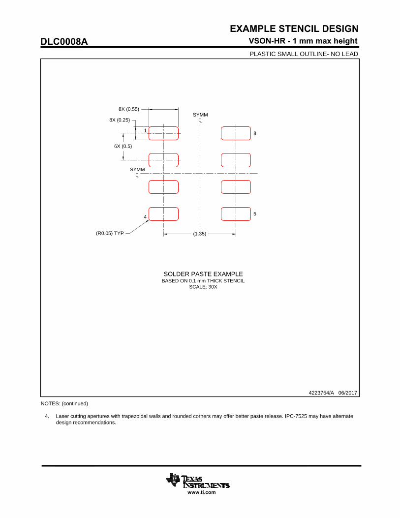
4. Laser cutting apertures with trapezoidal walls and rounded corners may offer better paste release. IPC-7525 may have alternate
design recommendations.
EXAMPLE STENCIL DESIGN
4223754/A 06/2017
www.ti.com
VSON-HR - 1 mm max height
DLC0008A
PLASTIC SMALL OUTLINE- NO LEAD
SOLDER PASTE EXAMPLE
BASED ON 0.1 mm THICK STENCIL
SCALE: 30X
SYMM
SYMM
(1.35)
6X (0.5)
8X (0.25)
8X (0.55)
4
1
5
8
(R0.05) TYP
IMPORTANT NOTICE
Texas Instruments Incorporated (TI) reserves the right to make corrections, enhancements, improvements and other changes to itssemiconductor products and services per JESD46, latest issue, and to discontinue any product or service per JESD48, latest issue. Buyersshould obtain the latest relevant information before placing orders and should verify that such information is current and complete.TI’s published terms of sale for semiconductor products (http://www.ti.com/sc/docs/stdterms.htm) apply to the sale of packaged integratedcircuit products that TI has qualified and released to market. Additional terms may apply to the use or sale of other types of TI products andservices.Reproduction of significant portions of TI information in TI data sheets is permissible only if reproduction is without alteration and isaccompanied by all associated warranties, conditions, limitations, and notices. TI is not responsible or liable for such reproduceddocumentation. Information of third parties may be subject to additional restrictions. Resale of TI products or services with statementsdifferent from or beyond the parameters stated by TI for that product or service voids all express and any implied warranties for theassociated TI product or service and is an unfair and deceptive business practice. TI is not responsible or liable for any such statements.Buyers and others who are developing systems that incorporate TI products (collectively, “Designers”) understand and agree that Designersremain responsible for using their independent analysis, evaluation and judgment in designing their applications and that Designers havefull and exclusive responsibility to assure the safety of Designers' applications and compliance of their applications (and of all TI productsused in or for Designers’ applications) with all applicable regulations, laws and other applicable requirements. Designer represents that, withrespect to their applications, Designer has all the necessary expertise to create and implement safeguards that (1) anticipate dangerousconsequences of failures, (2) monitor failures and their consequences, and (3) lessen the likelihood of failures that might cause harm andtake appropriate actions. Designer agrees that prior to using or distributing any applications that include TI products, Designer willthoroughly test such applications and the functionality of such TI products as used in such applications.TI’s provision of technical, application or other design advice, quality characterization, reliability data or other services or information,including, but not limited to, reference designs and materials relating to evaluation modules, (collectively, “TI Resources”) are intended toassist designers who are developing applications that incorporate TI products; by downloading, accessing or using TI Resources in anyway, Designer (individually or, if Designer is acting on behalf of a company, Designer’s company) agrees to use any particular TI Resourcesolely for this purpose and subject to the terms of this Notice.TI’s provision of TI Resources does not expand or otherwise alter TI’s applicable published warranties or warranty disclaimers for TIproducts, and no additional obligations or liabilities arise from TI providing such TI Resources. TI reserves the right to make corrections,enhancements, improvements and other changes to its TI Resources. TI has not conducted any testing other than that specificallydescribed in the published documentation for a particular TI Resource.Designer is authorized to use, copy and modify any individual TI Resource only in connection with the development of applications thatinclude the TI product(s) identified in such TI Resource. NO OTHER LICENSE, EXPRESS OR IMPLIED, BY ESTOPPEL OR OTHERWISETO ANY OTHER TI INTELLECTUAL PROPERTY RIGHT, AND NO LICENSE TO ANY TECHNOLOGY OR INTELLECTUAL PROPERTYRIGHT OF TI OR ANY THIRD PARTY IS GRANTED HEREIN, including but not limited to any patent right, copyright, mask work right, orother intellectual property right relating to any combination, machine, or process in which TI products or services are used. Informationregarding or referencing third-party products or services does not constitute a license to use such products or services, or a warranty orendorsement thereof. Use of TI Resources may require a license from a third party under the patents or other intellectual property of thethird party, or a license from TI under the patents or other intellectual property of TI.TI RESOURCES ARE PROVIDED “AS IS” AND WITH ALL FAULTS. TI DISCLAIMS ALL OTHER WARRANTIES ORREPRESENTATIONS, EXPRESS OR IMPLIED, REGARDING RESOURCES OR USE THEREOF, INCLUDING BUT NOT LIMITED TOACCURACY OR COMPLETENESS, TITLE, ANY EPIDEMIC FAILURE WARRANTY AND ANY IMPLIED WARRANTIES OFMERCHANTABILITY, FITNESS FOR A PARTICULAR PURPOSE, AND NON-INFRINGEMENT OF ANY THIRD PARTY INTELLECTUALPROPERTY RIGHTS. TI SHALL NOT BE LIABLE FOR AND SHALL NOT DEFEND OR INDEMNIFY DESIGNER AGAINST ANY CLAIM,INCLUDING BUT NOT LIMITED TO ANY INFRINGEMENT CLAIM THAT RELATES TO OR IS BASED ON ANY COMBINATION OFPRODUCTS EVEN IF DESCRIBED IN TI RESOURCES OR OTHERWISE. IN NO EVENT SHALL TI BE LIABLE FOR ANY ACTUAL,DIRECT, SPECIAL, COLLATERAL, INDIRECT, PUNITIVE, INCIDENTAL, CONSEQUENTIAL OR EXEMPLARY DAMAGES INCONNECTION WITH OR ARISING OUT OF TI RESOURCES OR USE THEREOF, AND REGARDLESS OF WHETHER TI HAS BEENADVISED OF THE POSSIBILITY OF SUCH DAMAGES.Unless TI has explicitly designated an individual product as meeting the requirements of a particular industry standard (e.g., ISO/TS 16949and ISO 26262), TI is not responsible for any failure to meet such industry standard requirements.Where TI specifically promotes products as facilitating functional safety or as compliant with industry functional safety standards, suchproducts are intended to help enable customers to design and create their own applications that meet applicable functional safety standardsand requirements. Using products in an application does not by itself establish any safety features in the application. Designers mustensure compliance with safety-related requirements and standards applicable to their applications. Designer may not use any TI products inlife-critical medical equipment unless authorized officers of the parties have executed a special contract specifically governing such use.Life-critical medical equipment is medical equipment where failure of such equipment would cause serious bodily injury or death (e.g., lifesupport, pacemakers, defibrillators, heart pumps, neurostimulators, and implantables). Such equipment includes, without limitation, allmedical devices identified by the U.S. Food and Drug Administration as Class III devices and equivalent classifications outside the U.S.TI may expressly designate certain products as completing a particular qualification (e.g., Q100, Military Grade, or Enhanced Product).Designers agree that it has the necessary expertise to select the product with the appropriate qualification designation for their applicationsand that proper product selection is at Designers’ own risk. Designers are solely responsible for compliance with all legal and regulatoryrequirements in connection with such selection.Designer will fully indemnify TI and its representatives against any damages, costs, losses, and/or liabilities arising out of Designer’s non-compliance with the terms and provisions of this Notice.
Mailing Address: Texas Instruments, Post Office Box 655303, Dallas, Texas 75265Copyright © 2018, Texas Instruments Incorporated