single phase multilevel inverter by using sinusoidal pulse
TRANSCRIPT

www.ijcrt.org © 2018 IJCRT | Volume 6, Issue 1 February 2018 | ISSN: 2320-2882
IJCRT1802093 International Journal of Creative Research Thoughts (IJCRT) www.ijcrt.org 737
Single Phase Multilevel Inverter By Using Sinusoidal
Pulse Width Modulation Technique
MURALI DASARI
Associate Professor
Department of Electrical & Electronics Engineering,
Geetanjali Institute of Science & Technology,
Gangavaram;Nellore,Nellore(Dt); A.P,India
MALLI SUMAN
PG Scholar
Department of Electrical & Electronics Engineering,
Geetanjali Institute of Science & Technology,
Gangavaram;Nellore,Nellore(Dt); A.P,India
Abstract: In this project, a novel multilevel inverter is proposed. The proposed multilevel inverter generates seven
levels AC output voltage with the appropriate gate signals design. Also, the low pass filter is used to reduce the total harmonic
distortion of the sinusoidal output voltage. The switching losses and the voltage stress of power devices can be reduced in the
proposed multi-level inverter. The operating principles of the proposed inverter and the voltage balancing method of input
capacitors are discussed. By using resonant switching capacitor converter, the voltage balance of input capacitors is achieved.
Sinusoidal pulse width modulation is used to control the multilevel inverter.
IndexTerms – Multilevel inverter, Sinusoidal Pulse Width Modulation,
I. INTRODUCTION
Now a days many industrial applications have begun to
require high power. Some appliances in the industries
however require medium or low power for their operation.
Using a high power source for all industrial loads may prove
beneficial to some motors requiring high power, while it may
damage the other loads. Some medium voltage motor drives
and utility applications require medium voltage. The
multilevel inverter has been introduced since 1975 as
alternative in high power and medium voltage situations. The
Multilevel inverter is like an inverter and it is used for
industrial applications as alternative in high power and
medium voltage situations.
The need of multilevel converter is to give a high output
power from medium voltage source. Sources like batteries,
super capacitors, solar panel are medium voltage sources.
The multi level inverter consists of several switches. In the
multi level inverter the arrangement switches angles are very
important.Problems can be reduced in multilevel inverter are
increases no of voltage level which leads to better voltage
waveforms. Reduces switching stresses on the device due to
the reduction of step voltage between the levels.
In this project, a novel multilevel inverter is proposed. The
proposed multilevel inverter generates seven levels AC
output voltage with the appropriate gate signals design. Also,
the low pass filter is used to reduce the total harmonic
distortion of the sinusoidal output voltage. The switching
losses and the voltage stress of power devices can be reduced
in the proposed multi-level inverter. The operating principles
of the proposed inverter and the voltage balancing method of
input capacitors are discussed. By using resonant switching
capacitor converter, the voltage balance of input capacitors is
achieved. Sinusoidal pulse width modulation is used to
control the multilevel inverter.
1.1 EXISTING SYSTEM
In the applications of inverters, the inverters with five
level inverter topology can produce output not as the high step-
up output voltage and with high number of switches Pulse-
width modulation (PWM), is a technique used to encode a
message into a pulsing signal. It is a type of modulation.
Although this modulation technique can be used to encode
information for transmission, its main use is to allow the control
of the power supplied to electrical devices, especially to inertial
loads such as motors.
1.2 PROPOSED SYSTEM In this project, multilevel DC-AC inverter is
introduced. The proposed multilevel inverter generates seven
levels AC output voltage with appropriate gate signal design.
Also, the low pass filter is used to reduce total harmonic
distortion of sinusoidal output voltage. The switching losses
and the voltage stress of power devices can be reduced in
proposed multi-level inverter. The operating principles of
proposed inverter and voltage balancing method of input
capacitors are presented. This multilevel inverter is controlled
with sinusoidal pulse-width modulation (SPWM).
The proposed multilevel inverter generates seven
levels AC output voltage with the appropriate gate signals
design. The low pass filter is used to reduce the input current
harmonics. Multi-level inverter concepts and voltage balancing
concepts on the input capacitors are proposed. The switching
losses and the voltage stress of power devices can be reduced in
the proposed multi-level inverter. By combining output
voltages in multilevel form, it has advantages of low dv/dt, low
input current distortion, and lower switching frequency. The
quality of electric power is higher than before. Because of the
www.ijcrt.org © 2018 IJCRT | Volume 6, Issue 1 February 2018 | ISSN: 2320-2882
IJCRT1802093 International Journal of Creative Research Thoughts (IJCRT) www.ijcrt.org 738
advancement of semiconductor, the specification of power
device and power conversion technique is promoted.
2. SEVEN LEVEL INVERTER TOPOLOGY 2.1 OPERATION OF PROPOSED TOPOLOGY
Fig.2.1 Proposed seven level inverter topology
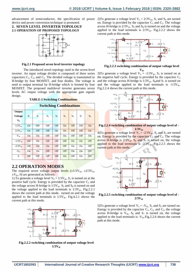
The introduced novel topology used in the seven-level
inverter. An input voltage divider is composed of three series
capacitors C1, C2, and C3. The divided voltage is transmitted to
H-bridge by four MOSFET, and four diodes. The voltage is
send to output terminal by H-bridge which is formed by four
MOSFET. The proposed multilevel inverter generates seven
levels AC output voltage with the appropriate gate signals
design.
TABLE-I Switching Combinations
Switching Combinations
Output
Voltage
V0
S1
S2
S3
S4
S5
S6
S7
S8
1/3Vdc On Off Off Off On Off Off On
2/3Vdc On Off Off On On Off Off On
Vdc On On Off Off On Off Off On
-1/3Vdc Off On Off Off Off On On Off
-2/3Vdc Off On On Off Off On On Off
-Vdc On On Off Off Off On On Off
0 Off Off Off Off On Off On Off
2.2 OPERATION MODES The required seven voltage output levels (±1/3Vdc, ±2/3Vdc,
±Vdc, 0) are generated as follows:
1).To generate a voltage level V0 = 1/3Vdc, S1 is turned on at the
positive half cycle. Energy is provided by the capacitor C1 and
the voltage across H-bridge is 1/3Vdc. S5 and S8 is turned on and
the voltage applied to the load terminals is 1/3Vdc. Fig.2.2.1
shows the current path at this mode. turned on and the voltage
applied to the load terminals is 1/3Vdc. Fig.4.2.1 shows the
current path at this mode.
Fig.2.2.2 switching combination of output voltage level
1/3Vdc
2)To generate a voltage level Vo = 2/3Vdc, S1 and S4 are turned
on. Energy is provided by the capacitor C1 and C2. The voltage
across H-bridge is 2/3Vdc. S5 and S8 is turned on and the voltage
applied to the load terminals is 2/3Vdc. Fig.2.2.2 shows the
current path at this mode.
Fig.2.2.3 switching combination of output voltage level
Vdc
3)To generate a voltage level Vo = -1/3Vdc, S2 is turned on at
the negative half cycle. Energy is provided by the capacitor C3
and the voltage across H-bridge is 1/3Vdc. S6and S7 is turned on
and the voltage applied to the load terminals is -1/3Vdc.
Fig.2.2.4 shows the current path at this mode.
Fig.2.2.4 switching combination of output voltage level of -
1/3Vdc
4)To generate a voltage level Vo = -2/3Vdc, S2 and S3 are turned
on. Energy is provided by the capacitor C2 and C3. The voltage
across H-bridge is 2/3Vdc. S6 and S7 is turned on, the voltage
applied to the load terminals is -2/3Vdc. Fig.2.2.5 shows the
current path at this mode.
Fig.2.2.5 switching combination of output voltage level of -
2/3Vdc
5)To generate a voltage level Vo = -Vdc, S1 and S2 are turned on.
Energy is provided by the capacitor C1, C2, and C3, the voltage
across H-bridge is Vdc, S6 and S7 is turned on, the voltage
applied to the load terminals is -Vdc.Fig.2.2.6 shows the current
path at this mode.

www.ijcrt.org © 2018 IJCRT | Volume 6, Issue 1 February 2018 | ISSN: 2320-2882
IJCRT1802093 International Journal of Creative Research Thoughts (IJCRT) www.ijcrt.org 738
Fig.2.2.6 Switching combination of output voltage level of -Vdc
6)To generate a voltage level Vo = 0, S5 and S7 are turned on.
The voltage applied to the load terminals is zero. Fig.2.2.7
shows the current path at this mode.
Fig2.2.7 switching combination of output voltage level of 0
the output current is increased. This inherent drawback is due
to a periodical forced charging and discharging operation in the
internal switched capacitors accompanied by a large capacitor
current, so that their efficiency cannot be increased by
decreasing its internal resistance. As a result, conventional
switched capacitor converters have been limited to be used with
a very small output current. This paper presents some novel
switched capacitor converter topologies that use a resonant
operation instead of the forced charging and discharging
operation. Their advantage over conventional switched
capacitor converters is a high efficiency even in a high output
current region
Since the voltage deviation causes larger harmonics
distortion in the output voltage, voltage balancing circuits are
indispensable for the capacitors in the multilevel inverters. By
using resonant switching capacitor converter, the voltage
balance of input capacitors is achieved. Fig.5.1 shows the
circuit configuration of a unit of the RSCC. The duty cycle of
every switch is equal to 50%. The voltage of C1 is higher than
the voltage of C2. Since the average current of C1 is higher than
that of C2 at one switching cycle, most of the charges flow from
C1 to C2. After few switching cycles, the voltage of C1 and C2
are equal. Fig. 5.1 shows the waveforms of the RSCC.
TABLE-II: Components Comparison between four
different seven-level inverters
TABLE-III: Voltage Stress Comparison between four
different seven-level inverters
3. VOLTAGE BALANCING CIRCUIT BASED ON
RSCC
Conventional switched capacitor converters have an
inherent drawback that their efficiency is much decreased as
the output current is increased. This inherent drawback is due
to a periodical forced charging and discharging operation in
the internal switched capacitors accompanied by a large
capacitor current, so that their efficiency cannot be increased
by decreasing its internal resistance. As a result, conventional
switched capacitor converters have been limited to be used
with a very small output current. This paper presents some
novel switched capacitor converter topologies that use a
resonant operation instead of the forced charging and
discharging operation. Their advantage over conventional
switched capacitor converters is a high efficiency even in a
high output current region
Since the voltage deviation causes larger harmonics
distortion in the output voltage, voltage balancing circuits are
indispensable for the capacitors in the multilevel inverters. By
using resonant switching capacitor converter, the voltage
balance of input capacitors is achieved. Fig.5.1 shows the
circuit configuration of a unit of the RSCC. The duty cycle of
every switch is equal to 50%. The voltage of C1 is higher than
the voltage of C2. Since the average current of C1 is higher
than that of C2 at one switching cycle, most of the charges
flow from C1 to C2. After few switching cycles, the voltage of
C1 and C2 are equal. Fig. 5.1 shows the waveforms of the
RSCC.
Fig.3.1 Circuit configuration of RSCC
www.ijcrt.org © 2018 IJCRT | Volume 6, Issue 1 February 2018 | ISSN: 2320-2882
IJCRT1802093 International Journal of Creative Research Thoughts (IJCRT) www.ijcrt.org 738
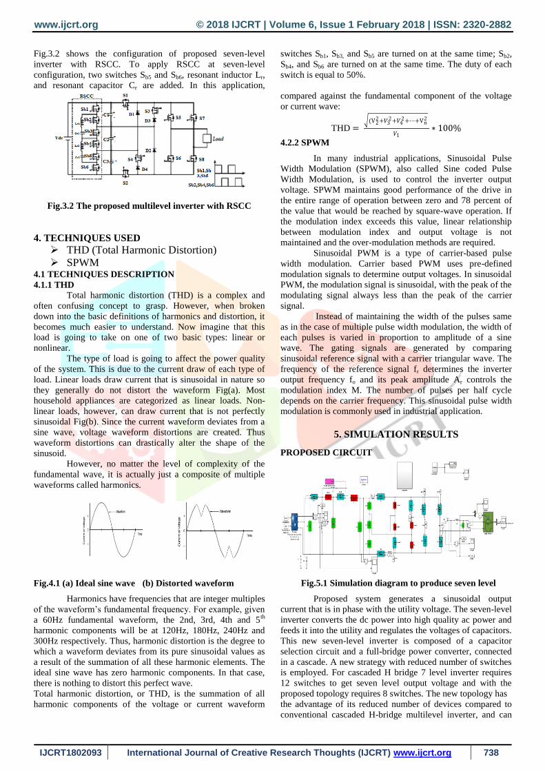
Fig.3.2 shows the configuration of proposed seven-level
inverter with RSCC. To apply RSCC at seven-level
configuration, two switches Sb5 and Sb6, resonant inductor Lr,
and resonant capacitor Cr are added. In this application,
switches Sb1, Sb3, and Sb5 are turned on at the same time; Sb2,
Sb4, and Sb6 are turned on at the same time. The duty of each
switch is equal to 50%.
Fig.3.2 The proposed multilevel inverter with RSCC
4. TECHNIQUES USED
THD (Total Harmonic Distortion)
SPWM 4.1 TECHNIQUES DESCRIPTION
4.1.1 THD
Total harmonic distortion (THD) is a complex and
often confusing concept to grasp. However, when broken
down into the basic definitions of harmonics and distortion, it
becomes much easier to understand. Now imagine that this
load is going to take on one of two basic types: linear or
nonlinear.
The type of load is going to affect the power quality
of the system. This is due to the current draw of each type of
load. Linear loads draw current that is sinusoidal in nature so
they generally do not distort the waveform Fig(a). Most
household appliances are categorized as linear loads. Non-
linear loads, however, can draw current that is not perfectly
sinusoidal Fig(b). Since the current waveform deviates from a
sine wave, voltage waveform distortions are created. Thus
waveform distortions can drastically alter the shape of the
sinusoid.
However, no matter the level of complexity of the
fundamental wave, it is actually just a composite of multiple
waveforms called harmonics.
Fig.4.1 (a) Ideal sine wave (b) Distorted waveform
Harmonics have frequencies that are integer multiples
of the waveform’s fundamental frequency. For example, given
a 60Hz fundamental waveform, the 2nd, 3rd, 4th and 5th
harmonic components will be at 120Hz, 180Hz, 240Hz and
300Hz respectively. Thus, harmonic distortion is the degree to
which a waveform deviates from its pure sinusoidal values as
a result of the summation of all these harmonic elements. The
ideal sine wave has zero harmonic components. In that case,
there is nothing to distort this perfect wave.
Total harmonic distortion, or THD, is the summation of all
harmonic components of the voltage or current waveform
compared against the fundamental component of the voltage
or current wave:
THD = (V2
2+𝑉32+𝑉4
2+⋯+Vn2
𝑉1∗ 100%
4.2.2 SPWM
In many industrial applications, Sinusoidal Pulse
Width Modulation (SPWM), also called Sine coded Pulse
Width Modulation, is used to control the inverter output
voltage. SPWM maintains good performance of the drive in
the entire range of operation between zero and 78 percent of
the value that would be reached by square-wave operation. If
the modulation index exceeds this value, linear relationship
between modulation index and output voltage is not
maintained and the over-modulation methods are required.
Sinusoidal PWM is a type of carrier-based pulse
width modulation. Carrier based PWM uses pre-defined
modulation signals to determine output voltages. In sinusoidal
PWM, the modulation signal is sinusoidal, with the peak of the
modulating signal always less than the peak of the carrier
signal.
Instead of maintaining the width of the pulses same
as in the case of multiple pulse width modulation, the width of
each pulses is varied in proportion to amplitude of a sine
wave. The gating signals are generated by comparing
sinusoidal reference signal with a carrier triangular wave. The
frequency of the reference signal fr determines the inverter
output frequency fo and its peak amplitude Ar controls the
modulation index M. The number of pulses per half cycle
depends on the carrier frequency. This sinusoidal pulse width
modulation is commonly used in industrial application.
5. SIMULATION RESULTS
PROPOSED CIRCUIT
Fig.5.1 Simulation diagram to produce seven level
Proposed system generates a sinusoidal output
current that is in phase with the utility voltage. The seven-level
inverter converts the dc power into high quality ac power and
feeds it into the utility and regulates the voltages of capacitors.
This new seven-level inverter is composed of a capacitor
selection circuit and a full-bridge power converter, connected
in a cascade. A new strategy with reduced number of switches
is employed. For cascaded H bridge 7 level inverter requires
12 switches to get seven level output voltage and with the
proposed topology requires 8 switches. The new topology has
the advantage of its reduced number of devices compared to
conventional cascaded H-bridge multilevel inverter, and can

www.ijcrt.org © 2018 IJCRT | Volume 6, Issue 1 February 2018 | ISSN: 2320-2882
IJCRT1802093 International Journal of Creative Research Thoughts (IJCRT) www.ijcrt.org 738
be extended to any number of levels. The schematic of the
cascaded H-bridge seven level inverter and proposed new
seven level topology built in MATLAB SIMULINK as shown
in fig.5.1.
SUBSYSTEM
Fig-5.6 FFT analysis with THD=20.47
Fig.5.2 Subsystem from main circuit
Fig.5.4 7-Level output Waveforms
Problems can be reduced in multilevel inverter
I/p current: Multilevel inverter can draw input current with
low distortion.
Switching frequency: Multilevel inverter can operate at
fundamental frequency and high switching frequency.
Conclusion
A Seven level inverter with reduced number of power
devices is designed
The reduction of power device is proved by comparing with
the traditional structures.
Fig-5.5 Solar Panel output Voltage and Current
Fig-5.3 Triggering Pulses for MOSFET

www.ijcrt.org © 2018 IJCRT | Volume 6, Issue 1 February 2018 | ISSN: 2320-2882
IJCRT1802093 International Journal of Creative Research Thoughts (IJCRT) www.ijcrt.org 738
References
[1] S. Kouro et al., “Recent advances and industrial
applications of multilevelconverters,” IEEE Trans. Ind.
Electron., vol. 57, no. 8, pp. 2553–2580,
Aug. 2010.
[2] H. Abu-Rub, J. Holtz, J. Rodriguez, and G. Baoming,
“Medium-voltage multilevel converters; state of the art,
challenges, and requirementsin industrial applications,”
IEEE Trans. Ind. Electron., vol. 57, no. 8,pp. 2581–2596,
Aug. 2010.
[3] Y. H. Liao and C. M. Lai, “Newly-constructed
simplified single-phasemulti-string multilevel inverter
topology for distributed energy resources,” IEEE Trans.
Power Electron., vol. 26, no. 9, pp. 2386–2391, Sep. 2011.
[4] L. Maharjan, S. Inoue, H. Akagi, and J. Asakura, “A
transformerless battery energy storage system based on a
multilevel cascade PWM converter,” in Proc. 39th Annu.
IEEE Power Electron. Conf., 2008, pp. 4798–4804.
[5] M. N. A. Kadir and Z. F. Hussien, “Asymmetrical
multilevel inverter: Maximum resolution for H-bridge
topology,” in Proc. Int. Conf. Power Electron. Drivers Syst.,
2005, pp. 1068–1071.
[6] M. Rotella, G. Penailillo, J. Pereda, and J. Dixon, “PWM
method to eliminate power sources in a non-redundant 27-
level inverter for machine drive applications,” IEEE Trans.
Ind. Electron., vol. 56, no. 1, pp. 194–201,
Jan. 2009.
[7] J. Dixon, M. Ortuizar, R. Carmi, P. Barriuso, P. Flores,
and L. Moran, “Static Var compensator and active power
filter with power injection capability, using 27-level
inverters and photovoltaic cells,” in Proc. IEEE Int. Symp.
Ind. Electron., 2006, pp. 1106–1111.
[8] J. Pereda and J. Dixon, “High-frequency link: A solution
for using only one DC source in asymmetric cascaded
multilevel inverters,” IEEE Trans.Ind. Electron., vol. 58,
no. 9, pp. 3884–3892, Sep. 2011.
[9] J. Pereda and J. Dixon, “23-level inverter for electric
vehicles using asingle battery pack and series active filters,”
IEEE Trans. Veh. Technol., vol. 61, no. 3, pp. 1043–1051,
Mar. 2012.
[10] Z. Du, L. M. Tolbert, J. N. Chiasson, and B. Ozpineci,
“A cascade multilevel inverter using a single DC source,” in
Proc. 21st Annu. IEEE Appl. Power Electron. Conf. Expo.,
2006, pp. 426–430.
[11] D. U. Zhong, B. Ozpineci, L. M. Tolbert, and J. N.
Chiasson, “DCAC cascaded H-bridge multilevel boost
inverter with no inductors forelectric/hybrid electric vehicle
applications,” IEEE Trans. Ind. Appl., vol.45, no. 3, pp.
963–970, May/Jun. 2009.
[12] H. Sepahvand, J. Liao, and M. Ferdowsi, “Investigation
on capacitor voltage regulation in cascaded H-bridge
multilevel converters with fundamental frequency
switching,” IEEE Trans. Ind. Electron., vol. 58, no. 11,
pp. 5102–5111, Nov. 2011.
[13] H. Sepahvand, J. Liao, M. Ferdowsi, and K. A Corzine,
“Capacitor voltageregulation in single-DC-source cascaded
H-bridge multilevel convertersusing phase-shift
modulation,” IEEE Trans. Ind. Electron., vol. 60, no. 9,
pp. 3619–3626, Sep. 2013.
[14] S. Vazquez, J. I. Leon, L. G. Franquelo, J. J. Padilla,
and J. M. Carrasco,“DC-voltage-ratio control strategy for
multilevel cascaded converters fedwith a single DC source,”
IEEE Trans. Ind. Electron., vol. 56, no. 7,pp. 2513–2521,
Jul. 2009.
[15] M. D. Seeman and S. R. Sanders, “Analysis and
optimization of switchedcapacitor DC-DC converters,”
IEEE Trans. Power Electron., vol. 23, no. 2, pp. 841–851,
Mar. 2008.
[16] J. C. Mayo-Maldonado, J. C. Rosas-Caro, and P.
Rapisarda, “Modeling approaches for DC-DC converters
with switched capacitors,” IEEE Trans. Ind. Electron., vol.
62, no. 2, pp. 953–959, Feb. 2015.
[17] M. Evzelman and S. Ben-Yaakov, “Average-current-
based conductionlosses model of switched capacitor
converters,” IEEE Trans. Power Electron., vol. 28, no. 7,
pp. 3341–3352, Jul. 2013.
[18] F. Zhang, L. Du, F. Z. Peng, and Z. Qian, “A new
design method forhigh-power high-efficiency switched-
capacitor dc–dc converters,” IEEE
Trans. Power Electron., vol. 23, no. 2, pp. 832–840, Mar.
2008.
[19] C.-K. Cheung, S.-C. Tan, C. Tse, and A. Ioinovici, “On
energy efficiencyof switched-capacitor converters,” IEEE
Trans. Power Electron., vol. 28,no. 2, pp. 862–876, Feb.
2013.

www.ijcrt.org © 2018 IJCRT | Volume 6, Issue 1 February 2018 | ISSN: 2320-2882
IJCRT1802093 International Journal of Creative Research Thoughts (IJCRT) www.ijcrt.org 738