single-ended, rail-to-rail i/o, low-gain pgaww1.microchip.com/downloads/en/devicedoc/21908a.pdf ·...
TRANSCRIPT

MCP6S91/2/3Single-Ended, Rail-to-Rail I/O, Low-Gain PGA
Features
• Multiplexed Inputs: 1 or 2 channels
• 8 Gain Selections:- +1, +2, +4, +5, +8, +10, +16 or +32 V/V
• Serial Peripheral Interface (SPI™)
• Rail-to-Rail Input and Output• Low Gain Error: ±1% (max.)• Offset Mismatch Between Channels: 0 µV
• High Bandwidth: 1 to 18 MHz (typ.)• Low Noise: 10 nV/√Hz @ 10 kHz (typ.)• Low Supply Current: 1.0 mA (typ.)
• Single Supply: 2.5V to 5.5V• Extended Temperature Range: -40°C to +125°C
Typical Applications
• A/D Converter Driver• Multiplexed Analog Applications
• Data Acquisition• Industrial Instrumentation• Test Equipment
• Medical Instrumentation
Block Diagram
Description
The Microchip Technology Inc. MCP6S91/2/3 areanalog Programmable Gain Amplifiers (PGAs). Theycan be configured for gains from +1 V/V to +32 V/V andthe input multiplexer can select one of up to two chan-nels through a SPI port. The serial interface can alsoput the PGA into shutdown to conserve power. ThesePGAs are optimized for high-speed, low offset voltageand single-supply operation with rail-to-rail input andoutput capability. These specifications support single-supply applications needing flexible performance ormultiple inputs.
The one-channel MCP6S91 and the two-channelMCP6S92 are available in 8-pin PDIP, SOIC and MSOPpackages. The two-channel MCP6S93 is available in a10-pin MSOP package. All parts are fully specified from-40°C to +125°C.
Package Types
VOUT
VREF
VDD
CSSI
SOSCK
CH1CH0
VSS
8RF
RG
MUX
SPI™Logic
GainSwitches
Resistor Ladder (R
LAD
)
VREF
CH0
VSS
SI
SCK
1
2
3
4
8
7
6
5
VDD
CS
VOUT
MCP6S91PDIP, SOIC, MSOP
CH1
CH0
VSS
SI
SCK
1
2
3
4
8
7
6
5
VDD
CS
VOUT
MCP6S92PDIP, SOIC, MSOP
CH0
VOUT
CH1
CS
1
2
3
4
10
9
8
7 SI
SCK
5 6
VREF
VDD
SO
VSS
MCP6S93MSOP
2004 Microchip Technology Inc. DS21908A-page 1

MCP6S91/2/3
1.0 ELECTRICAL CHARACTERISTICS
Absolute Maximum Ratings †
VDD – VSS ........................................................................7.0V
All inputs and outputs..................... VSS – 0.3V to VDD + 0.3V
Difference Input voltage ....................................... |VDD – VSS|
Output Short Circuit Current ..................................continuous
Current at Input Pin .............................................................±2 mA
Current at Output and Supply Pins ................................ ±30 mA
Storage temperature .....................................-65°C to +150°C
Junction temperature .................................................. +150°C
ESD protection on all pins (HBM; MM) ................ ≥4 kV; 200V
† Notice: Stresses above those listed under “MaximumRatings” may cause permanent damage to the device. This isa stress rating only and functional operation of the device atthose or any other conditions above those indicated in theoperational listings of this specification is not implied.Exposure to maximum rating conditions for extended periodsmay affect device reliability.
PIN FUNCTION TABLE
Name Function
VOUT Analog Output
CH0, CH1 Analog Inputs
VREF External Reference Pin
VSS Negative Power Supply
CS SPI Chip Select
SI SPI Serial Data Input
SO SPI Serial Data Output
SCK SPI Clock Input
VDD Positive Power Supply
DC CHARACTERISTICSElectrical Specifications: Unless otherwise indicated, TA = +25°C, VDD = +2.5V to +5.5V, VSS = GND, VREF = VSS, G = +1 V/V, Input = CH0 = (0.3V)/G, CH1 = 0.3V, RL = 10 kΩ to VDD/2, SI and SCK are tied low and CS is tied high.
Parameters Sym Min Typ Max Units ConditionsAmplifier Inputs (CH0, CH1)
Input Offset Voltage VOS -4 — +4 mV G = +1
Input Offset Voltage Mismatch ∆VOS — 0 — µV Between inputs (CH0, CH1)
Input Offset Voltage Drift ∆VOS/∆TA — ±1.8 — µV/°C TA = -40°C to +125°C
Power Supply Rejection Ratio PSRR 70 90 — dB G = +1 (Note 1)
Input Bias Current IB — ±1 — pA CHx = VDD/2
Input Bias Current at Temperature
IB — 30 — pA CHx = VDD/2, TA = +85°C
IB — 600 — pA CHx = VDD/2, TA = +125°C
Input Impedance ZIN — 1013||7 — Ω||pF
Input Voltage Range VIVR VSS − 0.3 — VDD + 0.3 V (Note 2)
Reference Input (VREF)
Input Impedance ZIN_REF — (5/G)||6 — kΩ||pF
Voltage Range VIVR_REF VSS — VDD V (Note 2)
Amplifier Gain
Nominal Gains G — 1 to 32 — V/V +1, +2, +4, +5, +8, +10, +16 or +32
DC Gain Error G = +1 gE -0.2 — +0.2 % VOUT ≈ 0.3V to VDD − 0.3V
G ≥ +2 gE -1.0 — +1.0 % VOUT ≈ 0.3V to VDD − 0.3V
DC Gain Drift G = +1 ∆G/∆TA — ±0.0002 — %/°C TA = -40°C to +125°C
G ≥ +2 ∆G/∆TA — ±0.0004 — %/°C TA = -40°C to +125°C
Note 1: RLAD (RF+RG in Figure 4-1) connects VREF, VOUT and the inverting input of the internal amplifier. The MCP6S92 has VREF tied internally to VSS, so VSS is coupled to the internal amplifier and the PSRR spec describes PSRR+ only. It is recommended that the MCP6S92’s VSS pin be tied directly to ground to avoid noise problems.
2: The MCP6S92’s VIVR and VIVR_REF are not tested in production; they are set by design and characterization.3: IQ includes current in RLAD (typically 60 µA at VOUT = 0.3V). Both IQ and IQ_SHDN exclude digital switching currents.
2004 Microchip Technology Inc. DS21908A-page 2

MCP6S91/2/3
Ladder Resistance
Ladder Resistance RLAD 3.4 4.9 6.4 kΩ (Note 1)
Ladder Resistance across Temperature
∆RLAD/∆TA — +0.028 — %/°C TA = -40°C to +125°C (Note 1)
Amplifier Output
DC Output Non-linearity G = +1 VONL — ±0.18 — % of FSR VOUT ≈ 0.3V to VDD − 0.3V, VDD = 5.0V
G ≥ +2 VONL — ±0.050 — % of FSR VOUT ≈ 0.3V to VDD − 0.3V, VDD = 5.0V
Maximum Output Voltage Swing VOH_ANA, VOL_ANA
VSS + 20 — VDD – 100 mV G ≥ +2; 0.5V output overdrive
VSS + 60 — VDD – 60 G ≥ +2; 0.5V output overdrive, VREF = VDD/2
Short Circuit Current ISC — ±25 — mA
Power Supply
Supply Voltage VDD 2.5 — 5.5 V
Minimum Valid Supply Voltage VDD_VAL — 0.4 2.0 V Register data still valid
Quiescent Current IQ 0.4 1.0 1.6 mA IO = 0 (Note 3)
Quiescent Current, Shutdown Mode
IQ_SHDN — 30 — pA IO = 0 (Note 3)
DC CHARACTERISTICS (CONTINUED)Electrical Specifications: Unless otherwise indicated, TA = +25°C, VDD = +2.5V to +5.5V, VSS = GND, VREF = VSS, G = +1 V/V, Input = CH0 = (0.3V)/G, CH1 = 0.3V, RL = 10 kΩ to VDD/2, SI and SCK are tied low and CS is tied high.
Parameters Sym Min Typ Max Units Conditions
Note 1: RLAD (RF+RG in Figure 4-1) connects VREF, VOUT and the inverting input of the internal amplifier. The MCP6S92 has VREF tied internally to VSS, so VSS is coupled to the internal amplifier and the PSRR spec describes PSRR+ only. It is recommended that the MCP6S92’s VSS pin be tied directly to ground to avoid noise problems.
2: The MCP6S92’s VIVR and VIVR_REF are not tested in production; they are set by design and characterization.3: IQ includes current in RLAD (typically 60 µA at VOUT = 0.3V). Both IQ and IQ_SHDN exclude digital switching currents.
2004 Microchip Technology Inc. DS21908A-page 3

MCP6S91/2/3
AC CHARACTERISTICSElectrical Specifications: Unless otherwise indicated, TA = +25°C, VDD = +2.5V to +5.5V, VSS = GND, VREF = VSS, G = +1 V/V, Input = CH0 = (0.3V)/G, CH1 = 0.3V, RL = 10 kΩ to VDD/2, CL = 60 pF, SI and SCK are tied low and CS is tied high.
Parameters Sym Min Typ Max Units ConditionsFrequency Response
-3 dB Bandwidth BW — 1 to 18 — MHz All gains; VOUT < 100 mVP-P (Note 1)
Gain Peaking GPK — 0 — dB All gains; VOUT < 100 mVP-P
Total Harmonic Distortion plus Noise
f = 20 kHz, G = +1 V/V THD+N — 0.0011 — % VOUT = 1.5V ± 1.0 VPK, VDD = 5.0V, BW = 80 kHz, RL = 10 kΩ to 1.5V
f = 20 kHz, G = +1 V/V THD+N — 0.0089 — % VOUT = 2.5V ± 1.0 VPK, VDD = 5.0V, BW = 80 kHz
f = 20 kHz, G = +4 V/V THD+N — 0.0045 — % VOUT = 2.5V ± 1.0 VPK, VDD = 5.0V, BW = 80 kHz
f = 20 kHz, G = +16 V/V THD+N — 0.028 — % VOUT = 2.5V ± 1.0 VPK, VDD = 5.0V, BW = 80 kHz
Step Response
Slew Rate SR — 4.0 — V/µs G = 1, 2
— 11 — V/µs G = 4, 5, 8, 10
— 22 — V/µs G = 16, 32
Noise
Input Noise Voltage Eni — 4.5 — µVP-P f = 0.1 Hz to 10 Hz (Note 2)
— 30 — f = 0.1 Hz to 200 kHz (Note 2)
Input Noise Voltage Density eni — 10 — nV/√Hz f = 10 kHz (Note 2)
Input Noise Current Density ini — 4 — fA/√Hz f = 10 kHz
Note 1: See Table 4-1 for a list of typical numbers and Figure 2-25 for the frequency response versus gain.2: Eni and eni include ladder resistance noise. See Figure 2-12 for eni versus G data.
2004 Microchip Technology Inc. DS21908A-page 4

MCP6S91/2/3
DIGITAL CHARACTERISTICSElectrical Specifications: Unless otherwise indicated, TA = 25°C, VDD = +2.5V to +5.5V, VSS = GND, VREF = VSS, G = +1 V/V, Input = CH0 = (0.3V)/G, CH1 = 0.3V, RL = 10 kΩ to VDD/2, CL = 60 pF, SI and SCK are tied low and CS is tied high.
Parameters Sym Min Typ Max Units Conditions
SPI Inputs (CS, SI, SCK)
Logic Threshold, Low VIL 0 — 0.3VDD V
Input Leakage Current IIL -1.0 — +1.0 µA
Logic Threshold, High VIH 0.7 VDD — VDD V
Amplifier Output Leakage Current — -1.0 — 1.0 µA In Shutdown mode
SPI Output (SO, for MCP6S93)
Logic Threshold, Low VOL_DIG VSS — VSS+0.4 V IOL = 2.1 mA, VDD = 5V
Logic Threshold, High VOH_DIG VDD – 0.5 — VDD V IOH = -400 µA
SPI Timing
Pin Capacitance CPIN — 10 — pF All digital I/O pins
Input Rise/Fall Times (CS, SI, SCK) tRFI — — 2 µs (Note 1)
Output Rise/Fall Times (SO) tRFO — 5 — ns MCP6S93
CS High Time tCSH 40 — — ns
SCK Edge to CS Fall Setup Time tCS0 10 — — ns SCK edge when CS is high
CS Fall to First SCK Edge Setup Time tCSSC 40 — — ns
SCK Frequency fSCK — — 10 MHz VDD = 5V (Note 2)
SCK High Time tHI 40 — — ns
SCK Low Time tLO 40 — — ns
SCK Last Edge to CS Rise Setup Time tSCCS 30 — — ns
CS Rise to SCK Edge Setup Time tCS1 100 — — ns SCK edge when CS is high
SI Setup Time tSU 40 — — ns
SI Hold Time tHD 10 — — ns
SCK to SO Valid Propagation Delay tDO — — 80 ns MCP6S93
CS Rise to SO Forced to Zero tSOZ — — 80 ns MCP6S93
Channel and Gain Select Timing
Channel Select Time tCH — 1.5 — µs CHx = 0.6V, CHy = 0.3V, G = 1, CHx to CHy select, CS = 0.7 VDD to VOUT 90% point
Gain Select Time tG — 1 — µs CHx = CHy = 0.3V, G = 5 to G = 1 select, CS = 0.7 VDD to VOUT 90% point
Shutdown Mode Timing
Out of Shutdown mode (CS goes high) to Amplifier Output Turn-on Time
tON — 3.5 10 µs CS = 0.7 VDD to VOUT 90% point
Into Shutdown mode (CS goes high) to Amplifier Output High-Z Turn-off Time
tOFF — 1.5 — µs CS = 0.7 VDD to VOUT 90% point
Note 1: Not tested in production. Set by design and characterization.2: When using the device in the daisy-chain configuration, maximum clock frequency is determined by a combination of
propagation delay time (tDO ≤ 80 ns), data input set-up time (tSU ≥ 40 ns), SCK high time (tHI ≥ 40 ns) and SCK rise and fall times of 5 ns. Maximum fSCK is therefore ≈ 5.8 MHz.
2004 Microchip Technology Inc. DS21908A-page 5

MCP6S91/2/3
TEMPERATURE CHARACTERISTICSElectrical Specifications: Unless otherwise indicated, VDD = +2.5V to +5.5V, VSS = GND.
Parameters Sym Min Typ Max Units Conditions
Temperature Ranges
Specified Temperature Range TA -40 — +125 °C (Note 1)
Operating Temperature Range TA -40 — +125 °C
Storage Temperature Range TA -65 — +150 °C
Thermal Package Resistances
Thermal Resistance, 8L-PDIP θJA — 85 — °C/W
Thermal Resistance, 8L-SOIC θJA — 163 — °C/W
Thermal Resistance, 8L-MSOP θJA — 206 — °C/W
Thermal Resistance, 10L-MSOP θJA — 143 — °C/W
Note 1: Operation in this range must not cause TJ to exceed Maximum Junction Temperature (+150°C).
2004 Microchip Technology Inc. DS21908A-page 6

MCP6S91/2/3
FIGURE 1-1: Channel Select Timing Diagram.
FIGURE 1-2: PGA Shutdown Timing Diagram (must enter correct commands before CS goes high).
FIGURE 1-3: Gain Select Timing Diagram.
FIGURE 1-4: Detailed SPI™ Serial Interface Timing; SPI 0,0 Mode.
CS
VOUT
tCH
0.6V0.3V
CS
tOFF
VOUT
tON
Hi-Z Hi-Z
ISS30 pA (typ.)
1.0 mA (typ.)
0.3V
CS
VOUT
tG
1.5V0.3V
CS
SCK
SI
tSU tHD
tCSSC tSCCS
tCSH
SO
(first 16 bits out are always zeros)
tDO tSOZ
tLO tHI
1/fSCK
tCS0tCS1
2004 Microchip Technology Inc. DS21908A-page 7

MCP6S91/2/3
FIGURE 1-5: Detailed SPI™ Serial Interface Timing; SPI 1,1 Mode.
1.1 DC Output Voltage Specs / Model
1.1.1 IDEAL MODEL
The ideal PGA output voltage (VOUT) is:
EQUATION 1-1:
(see Figure 1-6). This equation holds when there areno gain or offset errors and when the VREF pin is tied toa low-impedance source (<< 0.1Ω) at ground potential(VSS = 0V).
1.1.2 LINEAR MODEL
The PGA’s linear region of operation, including offsetand gain errors, is modeled by the line VO_LIN shown inFigure 1-6.
EQUATION 1-2:
The end points of this line are at VO_ID = 0.3V and VDD – 0.3V. Figure 1-6 shows the relationship betweenthe gain and offset specifications referred to in theelectrical specifications as follows:
EQUATION 1-3:
The DC Gain Drift (∆G/∆TA) can be calculated from thechange in gE across temperature. This is shown in thefollowing equation:
EQUATION 1-4:
CS
SCK
SI
tSU tHD
tCSSC tSCCS
SO
(first 16 bits out are always zeros)
tDO tSOZ
tHI tLO
1/fSCK
tCS1
tCSH
tCS0
Where:
G is the nominal gain
VO_ID GVIN= VREF VSS 0V= =
VO_LIN G 1 gE+( ) VIN0.3V
G----------- VOS+–
0.3V+=
VREF VSS 0V= =
gE 100%V2 V1–
G VDD 0.6V–( )--------------------------------------=
VOS
V1
G 1 gE+( )-------------------------= G +1=
G∆ TA∆⁄gE∆TA∆
----------=
2004 Microchip Technology Inc. DS21908A-page 8

MCP6S91/2/3
FIGURE 1-6: Output Voltage Model with the standard condition VREF = VSS = 0V.
1.1.3 OUTPUT NON-LINEARITY
Figure 1-7 shows the Integral Non-Linearity (INL) of theoutput voltage.
EQUATION 1-5:
The output non-linearity specification in the ElectricalSpecifications (with units of: % of FSR) is related toFigure 1-7 by:
EQUATION 1-6:
The Full-Scale Range (FSR) is VDD – 0.6V(0.3V to VDD – 0.3V).
FIGURE 1-7: Output Voltage INL with the standard condition VREF = VSS = 0 V.
1.1.4 DIFFERENT VREF CONDITIONS
Some of the plots in Section 2.0 “Typical PerformanceCurves”, have the conditions VREF = VDD/2 orVREF = VDD. The equations and figures above are easilymodified for these conditions. The ideal VOUT equationbecomes:
EQUATION 1-7:
The complete linear model is:
EQUATION 1-8:
where the new VIN end points are:
EQUATION 1-9:
The equations for extracting the specifications do notchange.
0
0
0.3
VDD – 0.3
VDD
V OUT
VOUT (V)
VIN (V)
0.3 VDD – 0.3 VDDGG G
V1
V O_I
D
V O_L
IN
V2
INL VOUT VO_LIN–=
VONL
max V3 V4,( )VDD 0.6V–------------------------------- 100%⋅=
0
INL (V)
VIN (V)0.3 VDD – 0.3 VDD
GG G0
V3
V4
VO_ID VREF G VIN VREF–( )+=
VDD VREF VSS 0V=>≥
VON_LIN G 1 gE+( ) VIN VIN_L VOS+–( ) 0.3V+=
VREF VSS 0V= =
VIN_L
0.3V VREF–
G------------------------------ VREF+=
VIN_H
VDD 0.3V– VREF–
G----------------------------------------------- VREF+=
2004 Microchip Technology Inc. DS21908A-page 9

MCP6S91/2/3
2.0 TYPICAL PERFORMANCE CURVES
Note: Unless otherwise indicated, TA = +25°C, VDD = +2.5V to +5.5V, VSS = GND, VREF = VSS, G = +1 V/V,Input = CH0 = (0.3V)/G, CH1 = 0.3V, RL = 10 kΩ to VDD/2 and CL = 60 pF.
FIGURE 2-1: DC Gain Error, G = +1.
FIGURE 2-2: DC Gain Error, G ≥ +2.
FIGURE 2-3: Ladder Resistance Drift.
FIGURE 2-4: DC Gain Drift, G = +1.
FIGURE 2-5: DC Gain Drift, G ≥ +2.
FIGURE 2-6: Crosstalk vs. Frequency (circuit in Figure 6-4).
Note: The graphs and tables provided following this note are a statistical summary based on a limited number ofsamples and are provided for informational purposes only. The performance characteristics listed hereinare not tested or guaranteed. In some graphs or tables, the data presented may be outside the specifiedoperating range (e.g., outside specified power supply range) and therefore outside the warranted range.
0%2%4%6%8%
10%12%14%16%18%20%22%24%
-0.1
0
-0.0
8
-0.0
6
-0.0
4
-0.0
2
0.00
0.02
0.04
0.06
0.08
0.10
DC Gain Error (%)
Per
cen
tag
e o
f O
ccu
rren
ces
600 SamplesG = +1
0%2%4%6%8%
10%12%14%16%18%
-0.6
-0.5
-0.4
-0.3
-0.2
-0.1 0.0
0.1
0.2
0.3
0.4
0.5
0.6
DC Gain Error (%)
Per
cen
tag
e o
f O
ccu
rren
ces 600 Samples
G ≥ +2
0%
2%
4%
6%
8%
10%
12%
14%
16%
0.01
9
0.02
0
0.02
1
0.02
2
0.02
3
0.02
4
0.02
5
0.02
6
0.02
7
0.02
8
0.02
9
0.03
0
Ladder Resistance Drift (%/°C)
Per
cen
tag
e o
f O
ccu
rren
ces
597 SamplesTA = -40 to +125°C
0%
5%
10%
15%
20%
25%
30%
35%
-0.0
006
-0.0
005
-0.0
004
-0.0
003
-0.0
002
-0.0
001
0.00
00
0.00
01
0.00
02
0.00
03
0.00
04
0.00
05
0.00
06
DC Gain Drift (%/°C)
Per
cen
tag
e o
f O
ccu
rren
ces
600 SamplesG = +1TA = -40 to +125°C
0%2%4%6%8%
10%12%14%16%18%20%22%24%26%
-0.0
020
-0.0
016
-0.0
012
-0.0
008
-0.0
004
0.00
00
0.00
04
0.00
08
0.00
12
0.00
16
0.00
20
DC Gain Drift (%/°C)
Per
cen
tag
e o
f O
ccu
rren
ces
600 SamplesG ≥ +2TA = -40 to +125°C
-100
-90
-80
-70
-60
-50
-40
-30
-20
-10
1.E+05 1.E+06 1.E+07 1.E+08
Frequency (Hz)
Cro
ssta
lk, I
np
ut
Ref
erre
d (
dB
) VDD = 5.0VG = +32 V/VCH0 selected
RS = 1 kΩ
RS = 0 Ω
RS = 100 Ω
RS = 10 kΩ
100k 100M10M1M
2004 Microchip Technology Inc. DS21908A-page 10

MCP6S91/2/3
Note: Unless otherwise indicated, TA = +25°C, VDD = +2.5V to +5.5V, VSS = GND, VREF = VSS, G = +1 V/V,Input = CH0 = (0.3V)/G, CH1 = 0.3V, RL = 10 kΩ to VDD/2 and CL = 60 pF.
FIGURE 2-7: Input Offset Voltage, VDD = 4.0V.
FIGURE 2-8: Input Offset Voltage Mismatch.
FIGURE 2-9: Input Noise Voltage Density vs. Frequency.
FIGURE 2-10: Input Offset Voltage Drift.
FIGURE 2-11: Input Offset Voltage vs. VREF Voltage.
FIGURE 2-12: Input Noise Voltage Density vs. Gain.
0%
5%
10%
15%
20%
25%
30%
-3 -2 -1 0 1 2 3Input Offset Voltage (mV)
Per
cen
tag
e o
f O
ccu
rren
ces 600 Samples
G = +1VDD = 4.0V
0%
5%
10%
15%
20%
25%
30%
35%
-30
-20
-10 0 10 20 30
Input Offset Voltage Mismatch (µV)
Per
cen
tag
e o
f O
ccu
rren
ces 32 Samples
VDD = 5.5VVIN = 0.3V
σ = 10.0 µVRMS
MeasurementRepeatability: 10.4 µVRMS
1
10
100
1000
0.1 1 10 100 1000 10000 100000
Frequency (Hz)
Inp
ut
No
ise V
olt
ag
e D
en
sit
y
(nV
/H
z)
1k 10k 100k1 10 1000.1
0%2%4%6%8%
10%12%14%16%18%20%22%24%
-10 -8 -6 -4 -2 0 2 4 6 8 10
Input Offset Voltage Drift (µV/°C)
Per
cen
tag
e o
f O
ccu
rren
ces
600 SamplesTA = -40 to +125°CG = +1
-3.0-2.5-2.0-1.5-1.0-0.50.00.51.01.52.02.53.0
0.0 0.5 1.0 1.5 2.0 2.5 3.0 3.5 4.0 4.5 5.0 5.5VREF Voltage (V)
Inp
ut
Off
set
Vo
ltag
e (m
V)
VDD = 5.5VVDD = 2.5V
G = +1VIN = VREF
0123456789
10111213
1 2 4 5 8 10 16 32
Gain (V/V)
Inp
ut
No
ise V
olt
ag
e D
en
sit
y
(nV
/H
z)
f = 10 kHz
2004 Microchip Technology Inc. DS21908A-page 11
MCP6S91/2/3
Note: Unless otherwise indicated, TA = +25°C, VDD = +2.5V to +5.5V, VSS = GND, VREF = VSS, G = +1 V/V,Input = CH0 = (0.3V)/G, CH1 = 0.3V, RL = 10 kΩ to VDD/2 and CL = 60 pF.
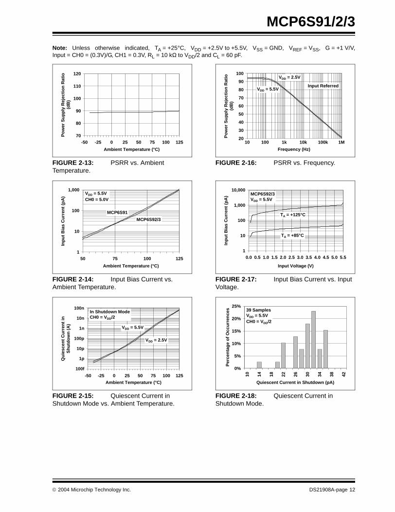
FIGURE 2-13: PSRR vs. Ambient Temperature.
FIGURE 2-14: Input Bias Current vs. Ambient Temperature.
FIGURE 2-15: Quiescent Current in Shutdown Mode vs. Ambient Temperature.
FIGURE 2-16: PSRR vs. Frequency.
FIGURE 2-17: Input Bias Current vs. Input Voltage.
FIGURE 2-18: Quiescent Current in Shutdown Mode.
70
80
90
100
110
120
-50 -25 0 25 50 75 100 125
Ambient Temperature (°C)
Po
wer
Su
pp
ly R
ejec
tio
n R
atio
(d
B)
1
10
100
1,000
50 75 100 125
Ambient Temperature (°C)
Inp
ut
Bia
s C
urr
ent
(pA
)
VDD = 5.5VCH0 = 5.0V
MCP6S92/3
MCP6S91
1.E-13
1.E-12
1.E-11
1.E-10
1.E-09
1.E-08
1.E-07
-50 -25 0 25 50 75 100 125
Ambient Temperature (°C)
Qu
iesc
ent
Cu
rren
t in
S
hu
tdo
wn
(A
)
In Shutdown ModeCH0 = VDD/2
VDD = 2.5V
VDD = 5.5V
100n
10n
1n
100p
10p
1p
100f
20
30
40
50
60
70
80
90
100
10 100 1000 10000 100000 1000000
Frequency (Hz)
Po
wer
Su
pp
ly R
ejec
tio
n R
atio
(d
B)
VDD = 5.5V
VDD = 2.5V
1k 10k 1M10 100
Input Referred
100k
1
10
100
1,000
10,000
0.0 0.5 1.0 1.5 2.0 2.5 3.0 3.5 4.0 4.5 5.0 5.5
Input Voltage (V)
Inp
ut
Bia
s C
urr
ent
(pA
)
TA = +85°C
MCP6S92/3VDD = 5.5V
TA = +125°C
0%
5%
10%
15%
20%
25%
10 14 18 22 26 30 34 38 42
Quiescent Current in Shutdown (pA)
Per
cen
tag
e o
f O
ccu
rren
ces 39 Samples
VDD = 5.5VCH0 = VDD/2
2004 Microchip Technology Inc. DS21908A-page 12

MCP6S91/2/3
Note: Unless otherwise indicated, TA = +25°C, VDD = +2.5V to +5.5V, VSS = GND, VREF = VSS, G = +1 V/V,Input = CH0 = (0.3V)/G, CH1 = 0.3V, RL = 10 kΩ to VDD/2 and CL = 60 pF.
FIGURE 2-19: Quiescent Current vs. Supply Voltage.
FIGURE 2-20: DC Output Non-Linearity vs. Supply Voltage.
FIGURE 2-21: Output Voltage Headroom vs. Output Plus Ladder Current (circuit in Figure 4-2).
FIGURE 2-22: Output Short Circuit Current vs. Supply Voltage.
FIGURE 2-23: DC Output Non-Linearity vs. Output Swing.
FIGURE 2-24: Output Voltage Swing vs. Frequency.
0.00.10.20.30.40.50.60.70.80.91.01.11.2
0.0 0.5 1.0 1.5 2.0 2.5 3.0 3.5 4.0 4.5 5.0 5.5
Supply Voltage (V)
Qu
iesc
ent
Cu
rren
t (m
A)
TA = +125°CTA = +85°CTA = +25°CTA = -40°C
0.001
0.01
0.1
1
2.5 3.0 3.5 4.0 4.5 5.0 5.5
Power Supply Voltage (V)
DC
Ou
tpu
t N
on
-Lin
eari
ty,
Inp
ut
Ref
erre
d (
% o
f F
SR
) VOUT = 0.3V to VDD - 0.3V
VONL/G, G = +1G = +2G ≥ +4
1
10
100
1000
0.1 1 10
Output Plus Ladder Current Magnitude (mA)
Ou
tpu
t V
olt
age
Hea
dro
om
; V
DD-V
OH a
nd
VO
L-V
SS (
mV
)
VDD = 5.5V
VDD = 2.5V
0
5
10
15
20
25
30
35
0.0 0.5 1.0 1.5 2.0 2.5 3.0 3.5 4.0 4.5 5.0 5.5Power Supply Voltage (V)
Ou
tpu
t S
ho
rt C
ircu
it C
urr
ent
Mag
nit
ud
e (m
A)
TA = +125°CTA = +85°CTA = +25°CTA = -40°C
0.001
0.01
0.1
1
1 10Output Voltage Swing (VP-P)
DC
Ou
tpu
t N
on
-Lin
eari
ty,
Inp
ut
Ref
erre
d (
% o
f F
SR
) VDD = 5.5V
VONL/G:G = +1G = +2G ≥ +4
0.1
1
10
1.E+05 1.E+06 1.E+07
Frequency (Hz)
Ou
tpu
t V
olt
age
Sw
ing
(V
P-P
)
100k 10M1M
VDD = 5.5V
VDD = 2.5V
G = 1, 2G = 4 to 10G = 16, 32
2004 Microchip Technology Inc. DS21908A-page 13

MCP6S91/2/3
Note: Unless otherwise indicated, TA = +25°C, VDD = +2.5V to +5.5V, VSS = GND, VREF = VSS, G = +1 V/V,Input = CH0 = (0.3V)/G, CH1 = 0.3V, RL = 10 kΩ to VDD/2 and CL = 60 pF.
FIGURE 2-25: Gain vs. Frequency.
FIGURE 2-26: Bandwidth vs. Capacitive Load.
FIGURE 2-27: THD plus Noise vs. Frequency, VOUT = 2 VP-P.
FIGURE 2-28: Gain Peaking vs. Capacitive Load.
FIGURE 2-29: The MCP6S91/2/3 family shows no phase reversal under overdrive.
FIGURE 2-30: THD plus Noise vs. Frequency, VOUT = 4 VP-P.
-20
-10
0
10
20
30
40
1.E+05 1.E+06 1.E+07 1.E+08
Frequency (Hz)
Gai
n (
dB
)
G = +2G = +1
1M 10M 100M100k
G = +32G = +16
G = +10G = +8G = +5G = +4
1
10
100
10 100 1000Capacitive Load (pF)
Ban
dw
idth
(M
Hz) G = +1
G = +4G = +16
0.0001
0.001
0.01
0.1
1
1.E+02 1.E+03 1.E+04 1.E+05
Frequency (Hz)
TH
D +
No
ise
(%)
100 1k 100k10k
G = +1, RL = 10 kΩ to 1.5V
G = +4
G = +1
G = +16
Measurement BW = 80 kHzVOUT = 2.0VP-P
VDD = 5.0V
0
1
2
3
4
5
6
7
10 100 1000
Capacitive Load (pF)
Gai
n P
eaki
ng
(d
B)
G = +16G = +4G = +1
-1
0
1
2
3
4
5
6
0 1 2 3 4 5 6 7 8 9 10
Time (1 µs/div)
Inp
ut,
Ou
tpu
t V
olt
age
(V)
VDD = 5.0VG = +1 V/V
VIN
VOUT
0.0001
0.001
0.01
0.1
1
1.E+02 1.E+03 1.E+04 1.E+05
Frequency (Hz)
TH
D +
No
ise
(%)
Measurement BW = 80 kHzVOUT = 4 VP-P
VDD = 5.0V
100 1k 100k10k
G = +4G = +1
G = +16
2004 Microchip Technology Inc. DS21908A-page 14

MCP6S91/2/3
Note: Unless otherwise indicated, TA = +25°C, VDD = +2.5V to +5.5V, VSS = GND, VREF = VSS, G = +1 V/V,Input = CH0 = (0.3V)/G, CH1 = 0.3V, RL = 10 kΩ to VDD/2 and CL = 60 pF.
FIGURE 2-31: Small-Signal Pulse Response.
FIGURE 2-32: Channel Select Timing.
FIGURE 2-33: Output Voltage vs. Shutdown Mode.
FIGURE 2-34: Large-Signal Pulse Response.
FIGURE 2-35: Gain Select Timing.
FIGURE 2-36: Minimum Valid Supply Voltage (register data still valid).
-60
-50
-40
-30
-20
-10
0
10
20
30
40
50
60
0.000 0.200 0.400 0.600 0.800 1.000 1.200 1.400 1.600 1.800 2.000
Time (200 ns/div)
Ou
tpu
t V
olt
age
(10
mV
/div
)
-300
-250
-200
-150
-100
-50
0
50
100
150
200
250
300
No
rmal
ized
Inp
ut
Vo
ltag
e (5
0 m
V/d
iv)
VDD = 5.0V
VOUT
G = +1G = +5G = +32
GVIN
0.25
0.30
0.35
0.40
0.45
0.50
0.55
0.60
0.65
0.00 0.50 1.00 1.50 2.00 2.50 3.00 3.50 4.00 4.50 5.00
Time (500 ns/div)
Ou
tpu
t V
olt
age
(V)
-20
-15
-10
-5
0
5
10
15
20
Ch
ip S
elec
t V
olt
age
(V)
5
0
VOUT
(CH0 = 0.6V,G = +1)
VOUT
(CH1 = 0.3V, G = +1)
CSCS
0.0
0.5
1.0
1.5
2.0
2.5
3.0
0.E+00 1.E+00 2.E+00 3.E+00 4.E+00 5.E+00 6.E+00 7.E+00 8.E+00 9.E+00 1.E+01 1.E+01 1.E+01
Time (1 µs/div)
Ou
tpu
t V
olt
age
(mV
)
-15
-10
-5
0
5
10
15
Ch
ip S
elec
t V
olt
age
(V)
VOUT is "ON"
Shutdown
CSCS
Shutdown VDD = 5.0VCH0 = 0.3VG = +1
0.0
0.5
1.0
1.5
2.0
2.5
3.0
3.5
4.0
4.5
5.0
0.0 0.5 1.0 1.5 2.0 2.5 3.0 3.5 4.0 4.5 5.0
Time (500 ns/div)
Ou
tpu
t V
olt
age
(V)
-2.5
-1.5
-0.5
0.5
1.5
2.5
3.5
4.5
5.5
6.5
7.5
No
rmal
ized
Inp
ut
Vo
ltag
e(1
V/d
iv)
VDD = 5.0V
GVIN
VOUT
G = +1G = +5G = +32
0.0
0.2
0.4
0.6
0.8
1.0
1.2
1.4
1.6
0 500 1000 1500 2000 2500 3000 3500 4000 4500 5000
Time (500 ns/div)
Ou
tpu
t V
olt
age
(V)
-20
-15
-10
-5
0
5
10
15
20
Ch
ip S
elec
t V
olt
age
(V)
VOUT
(CH0 = 0.3V, G = +5)
VOUT
(CH0 = 0.3V, G = +1)
CS CS
0%
10%20%30%
40%50%60%70%80%
90%
0.0
0.5
1.0
1.5
2.0
Minimum Valid Supply Voltage (V)
Per
cen
tag
e o
f O
ccu
rren
ces 32 Samples
1st Wafer Lot
2004 Microchip Technology Inc. DS21908A-page 15

MCP6S91/2/3
Note: Unless otherwise indicated, TA = +25°C, VDD = +2.5V to +5.5V, VSS = GND, VREF = VSS, G = +1 V/V,Input = CH0 = (0.3V)/G, CH1 = 0.3V, RL = 10 kΩ to VDD/2 and CL = 60 pF.
FIGURE 2-37: Input Offset Voltage vs. Input Voltage, VDD = 2.5V.
FIGURE 2-38: Output Voltage Headroom vs. Ambient Temperature.
FIGURE 2-39: Input Offset Voltage vs. Input Voltage, VDD = 5.5V.
0.00.10.20.30.40.50.60.70.80.91.01.11.2
0.0 0.5 1.0 1.5 2.0 2.5
Input Voltage (V)
Inp
ut
Off
set
Vo
ltag
e (m
V) G = 1 V/V
VDD = 2.5VTA = +125°CTA = +85°CTA = +25°CTA = -40°C
0
5
10
15
20
25
30
35
-50 -25 0 25 50 75 100 125
Ambient Temperature (°C)
Ou
tpu
t V
olt
age
Hea
dro
om
;V
DD–V
OH a
nd
VO
L–V
SS (
mV
)
VDD = 5.5V: VDD–VOH
VOL–VSS
VDD = 2.5V: VDD–VOH
VOL–VSS
VREF = VSS
0.00.10.20.30.40.50.60.70.80.91.01.11.2
0.0 0.5 1.0 1.5 2.0 2.5 3.0 3.5 4.0 4.5 5.0 5.5
Input Voltage (V)
Inp
ut
Off
set
Vo
ltag
e (m
V) G = 1 V/V
VDD = 5.5V
TA = +125°CTA = +85°CTA = +25°CTA = -40°C
2004 Microchip Technology Inc. DS21908A-page 16

MCP6S91/2/3
3.0 PIN DESCRIPTIONS
Descriptions of the pins are listed in Table 3-1.
TABLE 3-1: PIN FUNCTION TABLE
3.1 Analog Output
The output pin (VOUT) is a low-impedance voltagesource. The selected gain (G), selected input (CH0,CH1) and voltage at VREF determine its value.
3.2 Analog Inputs (CH0, CH1)
The inputs CH0 and CH1 connect to the signalsources. They are high-impedance CMOS inputs withlow bias currents. The internal MUX selects which oneis amplified to the output.
3.3 External Reference Voltage (VREF)
The VREF pin, which is an analog input, should be at avoltage between VSS and VDD (the MCP6S92 hasVREF tied internally to VSS). The voltage at this pinshifts the output voltage.
3.4 Power Supply (VSS and VDD)
The Positive Power Supply Pin (VDD) is 2.5V to 5.5Vhigher than the Negative Power Supply Pin (VSS). Fornormal operation, the other pins are at voltagesbetween VSS and VDD.
Typically, these parts are used in a single (positive)supply configuration. In this case, VSS is connected toground and VDD is connected to the supply. VDD willneed a local bypass capacitor (typically 0.01 µF to0.1 µF) within 2 mm of the VDD pin. These parts canshare a bulk capacitor with analog parts (typically2.2 µF to 10 µF) within 100 mm of the VDD pin.
3.5 Digital Inputs
The SPI interface inputs are: Chip Select (CS), SerialInput (SI) and Serial Clock (SCK). These are Schmitt-triggered, CMOS logic inputs.
3.6 Digital Output
The MCP6S93 device has a SPI interface Serial Output(SO) pin. This is a CMOS push-pull output and doesnot ever go High-Z. Once the device is deselected (CSgoes high), SO is forced low. This feature supportsdaisy-chaining, as explained in Section 5.3 “Daisy-Chain Configuration”.
MCP6S91 MCP6S92 MCP6S93 Symbol Description
1 1 1 VOUT Analog Output
2 2 2 CH0 Analog Input
— 3 3 CH1 Analog Input
3 — 4 VREF External Reference Pin
4 4 5 VSS Negative Power Supply
5 5 6 CS SPI™ Chip Select
6 6 7 SI SPI Serial Data Input
— — 8 SO SPI Serial Data Output
7 7 9 SCK SPI Clock Input
8 8 10 VDD Positive Power Supply
2004 Microchip Technology Inc. DS21908A-page 17

MCP6S91/2/3
4.0 ANALOG FUNCTIONS
The MCP6S91/2/3 family of Programmable GainAmplifiers (PGA) is based on simple analog buildingblocks (see Figure 4-1). Each of these blocks will beexplained in more detail in the following subsections.
FIGURE 4-1: PGA Block Diagram.
4.1 Input MUX
The MCP6S91 has one input, while the MCP6S92 andMCP6S93 have two inputs (see Figure 4-1).
For the lowest input current, float unused inputs. Tyingthese pins to a voltage near the active channel’s biasvoltage also works well. For simplicity, they can be tiedto VSS or VDD, but the input current may increase.
The one-channel MCP6S91 has approximately thesame input bias current as the two-channel MCP6S92and MCP6S93.
The input offset voltage mismatch between channels(∆VOS) is, ideally, 0 µV. The input MUX uses CMOStransmission gates that have drain-source (channel)resistance, but no offset voltage. The histogram inFigure 2-8 reflects the measurement repeatability(i.e., noise power bandwidth) rather than the actualmismatch. Reducing the measurement bandwidth willproduce a more narrow histogram and give an aver-age closer to 0 µV.
4.2 Internal Op Amp
The internal op amp gives the right combination ofbandwidth, accuracy and flexibility.
4.2.1 COMPENSATION CAPACITORS
The internal op amp has three compensation capaci-tors (comp. caps.) connected to a switching network.They are selected to give good small-signal bandwidthat high gains and good slew rates (full-power band-width) at low gains. The change in bandwidth as gainchanges is between 2 and 12 MHz. Refer to Table 4-1for more information.
TABLE 4-1: GAIN VS. INTERNAL COMPENSATION CAPACITOR
4.2.2 RAIL-TO-RAIL CHANNEL INPUTS
The input stage of the internal op amp uses two differ-ential input stages in parallel; one operates at low VIN(input voltage), while the other operates at high VIN.With this topology, the internal inputs can operate to0.3V past either supply rail. The input offset voltage ismeasured at both VIN = VSS – 0.3V and VDD + 0.3V toensure proper operation.
The transition between the two input stages occurswhen VIN ≈ VDD – 1.5V. For the best distortion and gainlinearity, avoid this region of operation.
MCP6S91 – One input (CH0), no SO pin
MCP6S92 – Two inputs (CH0, CH1), VREF tiedinternally to VSS, no SO pin
MCP6S93 – Two inputs (CH0, CH1)
VOUT
VREF
VDD
CSSI
SOSCK
CH1CH0
VSS
8RF
RG
MUX
SPI™Logic
GainSwitches
Resistor Ladder (R
LAD )
Gain(V/V)
InternalComp.Cap.
GBWP(MHz)Typ.
SR(V/µs)Typ.
FPBW(MHz)Typ.
BW(MHz)Typ.
1 Large 12 4.0 0.30 12
2 Large 12 4.0 0.30 6
4 Medium 20 11 0.70 10
5 Medium 20 11 0.70 7
8 Medium 20 11 0.70 2.4
10 Medium 20 11 0.70 2.0
16 Small 64 22 1.6 5
32 Small 64 22 1.6 2.0
Note 1: FPBW is the Full-Power Bandwidth. These numbers are based on VDD = 5.0V.
2: No changes in DC performance (e.g., VOS) accompany a change in compensation capacitor.
3: BW is the closed-loop, small signal -3 dB bandwidth.
2004 Microchip Technology Inc. DS21908A-page 18

MCP6S91/2/3
4.2.3 RAIL-TO-RAIL OUTPUT
The maximum output voltage swing is the maximumswing possible under a particular amplifier load current.The amplifier load current is the sum of the externalload current (IOUT) and the current through the ladderresistance (ILAD); see Figure 4-2.
EQUATION 4-1:
FIGURE 4-2: Amplifier Load Current.
See Figure 2-21 for the typical output headroom(VDD – VOH or VOL – VSS) as a function of amplifierload current.
The specification table states the output can reachwithin 60 mV of either supply rail when RL = 10 kΩ andVREF = VDD/2.
4.2.4 INPUT VOLTAGE AND PHASE REVERSAL
The MCP6S91/2/3 amplifier family is designed withCMOS input devices. It is designed to not exhibit phaseinversion when the input pins exceed the supplyvoltages. Figure 2-29 shows an input voltageexceeding both supplies with no resulting phaseinversion.
The maximum voltage that can be applied to the inputpins (CHx) is VSS – 0.3V to VDD + 0.3V. Voltages onthe inputs that exceed this absolute maximum ratingcan cause excessive current to flow into or out of theinput pins. Current beyond ±2 mA can cause possiblereliability problems. Applications that exceed this ratingmust be externally limited with an input resistor, asshown in Figure 4-3.
FIGURE 4-3: RIN limits the current flow into an input pin.
4.3 Resistor Ladder
The resistor ladder shown in Figure 4-1(RLAD = RF + RG) sets the gain. Placing the gainswitches in series with the inverting input reduces theparasitic capacitance, distortion and gain mismatch.
RLAD is an additional load on the output of the PGA andcauses additional current draw from the supplies. It isalso a load (ZIN_REF) on the external circuitry drivingthe VREF pin.
In Shutdown mode, RLAD is still attached to the VOUTand VREF pins. Thus, these pins and the internal ampli-fier’s inverting input are all connected through RLADand the output is not High-Z (unlike the internal opamp).
While RLAD contributes to the output noise, its effect issmall. Refer to Figure 2-12.
Where:
Amplifier Load Current IOUT ILAD+=
ILAD
VOUT VREF–( )RLAD
-------------------------------------=
VOUT
VREF
RLAD
IOUT
ILAD
MCP6S9X
CHx
RIN
VIN
RIN ≥VSS – (Maximum expected VIN)
2 mA
RIN ≥(Maximum expected VIN) – VDD
2 mA
VOUT
2004 Microchip Technology Inc. DS21908A-page 19
MCP6S91/2/3
4.4 Rail-to-Rail VREF Input
The VREF input is intended to be driven by a low-impedance voltage source. The source driving theVREF pin should have an output impedance less than0.1Ω to maintain reasonable gain accuracy. The supplyvoltage VSS and VDD usually meet this requirement.
RLAD presents a load at the VREF pin to the externalcircuit (ZIN_REF ≈ (5 kΩ/G)||(6 pF)), which depends onthe gain. Any source driving the VREF pin must becapable of driving a load as heavy as 0.16 kΩ||6 pF(G = 32).
The absolute maximum voltages that can be applied tothe reference input pin (VREF) are VSS – 0.3V andVDD + 0.3V. Voltages on the inputs that exceed thisabsolute maximum rating can cause excessive currentto flow into or out of this pin. Current beyond ±2 mA cancause possible reliability problems. Because anexternal series resistor cannot be used (for low gainerror), the external circuit must ensure that VREF isbetween VSS – 0.3V and VDD + 0.3V.
The VIVR_REF spec shows the region of normaloperation for the VREF pin (VSS to VDD). Staying withinthis region ensures proper operation of the PGA and itssurrounding circuitry.
4.5 Shutdown Mode
These PGAs use a software shutdown command.When the SPI interface sends a shutdown command,the internal op amp is shut down and its output placedin a High-Z state.
The resistive ladder is always connected betweenVREF and VOUT; even in shutdown. This means that theoutput resistance will be on the order of 5 kΩ, with apath for output signals to appear at the input.
2004 Microchip Technology Inc. DS21908A-page 20

MCP6S91/2/3
5.0 DIGITAL FUNCTIONS
The MCP6S91/2/3 PGAs use a standard SPIcompatible serial interface to receive instructions froma controller. This interface is configured to allow daisy-chaining with other SPI devices.
5.1 SPI Timing
Chip Select (CS) toggles low to initiate communica-tion with these devices. The first byte of each SI word(two bytes long) is the instruction byte, which goesinto the Instruction register. The Instruction registerpoints the second byte to its destination. In a typicalapplication, CS is raised after one word (16 bits) toimplement the desired changes. Section 5.3 “Daisy-
Chain Configuration”, covers applications usingmultiple 16-bit words. SO goes low after CS goeshigh; it has a push-pull output that does not go into ahigh-Z state.
The MCP6S91/2/3 devices operate in SPI modes 0,0and 1,1. In 0,0 mode, the clock idles in the low state(Figure 5-1). In 1,1 mode, the clock idles in the highstate (Figure 5-2). In both modes, SI data is loaded intothe PGA on the rising edge of SCK, while SO data isclocked out on the falling edge of SCK. In 0,0 mode, thefalling edge of CS also acts as the first falling edge ofSCK (see Figure 5-1). There must be multiples of 16clocks (SCK) while CS is low or commands will abort(see Section 5.3 “Daisy-Chain Configuration”).
FIGURE 5-1: Serial Bus Sequence for the PGA; SPI™ 0,0 Mode (see Figure 1-4).
FIGURE 5-2: Serial Bus Sequence for the PGA; SPI™ 1,1 Mode (see Figure 1-5).
1 2 3 4 5 6 7 8 9 10 11 12 13 14 15 16
bit 7
CS
SCK
SI
Instruction Byte Data Byte
bit 0
bit 7
bit 0
SO
(first 16 bits out are always zeros)
1 2 3 4 5 6 7 8 9 10 11 12 13 14 15 16
bit 7
CS
SCK
SI
Instruction Byte Data Byte
bit 0
bit 7
bit 0
SO
(first 16 bits out are always zeros)
2004 Microchip Technology Inc. DS21908A-page 21

MCP6S91/2/3
5.2 Registers
The analog functions are programmed through the SPIinterface using 16-bit words (see Figure 5-1 andFigure 5-2). This data is sent to two of three 8-bit regis-ters: Instruction register (Register 5-1), Gain register(Register 5-2) and Channel register (Register 5-3).There are no power-up defaults for these threeregisters.
5.2.1 ENSURING VALID DATA IN THE REGISTERS
After power up, the registers contain random data thatmust be initialized. Sending valid gain and channelselection commands to the internal registers puts validdata into those registers. Also, the internal statemachine starts in an arbitrary state. Toggling the ChipSelect pin (CS) from high to low, then back to highagain, puts the internal state machine in a known, validcondition (this can be done by entering any validcommand).
After power-up, and when the power supply voltagedips below the minimum valid VDD (VDD_VAL), the inter-nal register data and state machine may need to bereset. This is accomplished as described before. Usean external system supervisor to detect these eventsso that the microcontroller will reset the PGA state andregisters.
A 0.1 µF bypass capacitor mounted as close aspossible to the VDD pin provides additional transientimmunity.
5.2.2 INSTRUCTION REGISTER
The Instruction register has 3 command bits and 1 indi-rect address bit; see Register 5-1. The command bitsinclude a NOP (000) to support daisy-chaining (seeSection 5.3 “Daisy-Chain Configuration”); the otherNOP commands shown should not be used (they arereserved for future use). The device is brought out ofShutdown mode when a valid command, other thanNOP or Shutdown, is sent and CS is raised.
REGISTER 5-1: INSTRUCTION REGISTERW-0 W-0 W-0 U-x U-x U-x U-x W-0
M2 M1 M0 — — — — A0
bit 7 bit 0
bit 7-5 M2-M0: Command bits000 = NOP (Note 1)001 = PGA enters Shutdown mode as soon as a full 16-bit word is sent and CS is raised.
(Notes 1 and 2)010 = Write to register.011 = NOP (reserved for future use) (Note 1)1XX = NOP (reserved for future use) (Note 1)
bit 4-1 Unimplemented: Read as ‘0’ (reserved for future use)
bit 0 A0: Indirect Address bit1 = Addresses the Channel register0 = Addresses the Gain register
Note 1: All other bits in the 16-bit word (including A0) are “don’t cares.”
2: The device exits Shutdown mode when a valid command (other than NOP or Shutdown) is sent and CS is raised; that valid command will be executed. Shutdown does not toggle.
Legend:
R = Readable bit W = Writable bit U = Unimplemented bit, read as ‘0’
-n = Value at POR ‘1’ = Bit is set ‘0’ = Bit is cleared x = Bit is unknown
2004 Microchip Technology Inc. DS21908A-page 22

MCP6S91/2/3
5.2.3 SETTING THE GAIN
The amplifier can be programmed to produce binaryand decimal gain settings between +1 V/V and +32 V/V.Register 5-2 shows the details. At the same time, differ-ent compensation capacitors are selected to optimizethe bandwidth vs. slew rate trade-off (see Table 4-1).
REGISTER 5-2: GAIN REGISTERU-x U-x U-x U-x U-x W-0 W-0 W-0
— — — — — G2 G1 G0
bit 7 bit 0
bit 7-3 Unimplemented: Read as ‘0’ (reserved for future use)
bit 2-0 G2-G0: Gain Select bits000 = Gain of +1001 = Gain of +2010 = Gain of +4011 = Gain of +5100 = Gain of +8101 = Gain of +10110 = Gain of +16111 = Gain of +32
Legend:
R = Readable bit W = Writable bit U = Unimplemented bit, read as ‘0’
-n = Value at POR ‘1’ = Bit is set ‘0’ = Bit is cleared x = Bit is unknown
2004 Microchip Technology Inc. DS21908A-page 23

MCP6S91/2/3
5.2.4 CHANGING THE CHANNEL
If the Instruction register is programmed to address theChannel register, the multiplexed inputs of theMCP6S92 and MCP6S93 can be changed usingRegister 5-3.
REGISTER 5-3: CHANNEL REGISTERU-x U-x U-x U-x U-x U-x U-x W-0
— — — — — — — C0
bit 7 bit 0
bit 7-1 Unimplemented: Read as ‘0’ (reserved for future use)
bit 0 C0: Channel Select bit
0 =1 =
MCP6S91CH0CH0
MCP6S92CH0
CH1
MCP6S93CH0
CH1
Legend:
R = Readable bit W = Writable bit U = Unimplemented bit, read as ‘0’
-n = Value at POR ‘1’ = Bit is set ‘0’ = Bit is cleared x = Bit is unknown
2004 Microchip Technology Inc. DS21908A-page 24

MCP6S91/2/3
5.2.5 SHUTDOWN COMMAND
The software shutdown command allows the user toput the amplifier into a low-power mode (seeRegister 5-1). In this Shutdown mode, most pins arehigh-impedance (Section 4.5 “Shutdown Mode” andSection 5.1 “SPI Timing” cover the exceptions at pinsVREF, VOUT and SO).
Once the PGA has entered Shutdown mode, it willremain in this mode until either a valid command is sentto the device (other than NOP or Shutdown) or thedevice is powered down and back up again. Theinternal registers maintain their values while inshutdown.
Once brought out of Shutdown mode, the part returnsto its previous state (see Section 5.2.1 “EnsuringValid Data in the Registers” for exceptions to thisrule). This makes it possible to bring the device out ofshutdown mode using one command; send a com-mand to select the current channel (or gain) and thedevice will exit shutdown with the same state thatexisted before shutdown.
5.3 Daisy-Chain Configuration
Multiple MCP6S91/2/3 devices can be connected in adaisy-chain configuration by connecting the SO pinfrom one device to the SI pin on the next device andusing common SCK and CS lines (Figure 5-3). Thisapproach reduces PCB layout complexity and usesfewer PICmicro® microcontroller I/O pins.
The example in Figure 5-3 shows a daisy-chainconfiguration with two devices, although any number ofdevices can be configured this way. The MCP6S91 andMCP6S92 can only be used at the far end of the daisy-chain, because they do not have a serial data out (SO)pin. As shown in Figure 5-4 and Figure 5-5, both SI andSO data are sent in 16-bit (2 byte) words. Thesedevices abort any command that is not a multiple of 16bits.
When using the daisy-chain configuration, the maxi-mum clock speed possible is reduced to ≈ 5.8 MHz dueto the SO pin’s propagation delay (see ElectricalSpecifications).
The internal SPI shift register is automatically loadedwith zeros whenever CS goes high (a command isexecuted). Thus, the first 16-bits out of the SO pin afterthe CS line goes low are always zeros. This means thatthe first command loaded into the next device in thedaisy-chain is a NOP. This feature makes it possible tosend shorter command and data byte strings when thefarthest devices do not need to change. For example, ifthere were three devices on the chain, and only themiddle device needed changing, then only 32 bytes ofdata need to be transmitted (for the first and middledevices). The last device on the chain would receive aNOP when the CS pin is raised to execute thecommand.
FIGURE 5-3: Daisy-Chain Configuration.
PICmicro®
SO
CSSCKSI
CSSCK
SO
Device 1
Device 1
00100000 00000000
SO
CSSCKSIDevice 2
Device 2
00000000 00000000
Device 1
01000001 00000111
Device 2
00100000 00000000
4. Clock out the instruction and data for Device 1 (16 clocks) to Device 1.5. Device 1 automatically shifts data from Device 1 to Device 2 (16 clocks).6. Raise CS.
1. Set CS low.2. Clock out the instruction and data for device 2 (16 clocks) to Device 1.3. Device 1 automatically clocks out all zeros (first 16 clocks) to Device 2.
Microcontroller
2004 Microchip Technology Inc. DS21908A-page 25

MCP6S91/2/3
FIGURE 5-4: Serial Bus Sequence for Daisy-Chain Configuration; SPI™ 0,0 Mode.
FIGURE 5-5: Serial Bus Sequence for Daisy-Chain Configuration; SPI™ 1,1 Mode.
1 2 3 4 5 6 7 8 9 10111213141516
bit 7
CS
SCK
SI
Instruction Byte Data Byte
bit 0
bit 7
bit 0
SO
(first 16 bits out are always zeros)
1 2 3 4 5 6 7 8 9 10111213141516
bit 7
Instruction Byte Data Byte
bit 0
bit 7
bit 0
for Device 2 for Device 2 for Device 1 for Device 1
bit 7
Instruction Byte Data Byte
bit 0
bit 7
bit 0
for Device 2 for Device 2
1 2 3 4 5 6 7 8 9 10111213141516
bit 7
CS
SCK
SI
Instruction Byte Data Byte
bit 0
bit 7
bit 0
SO
(first 16 bits out are always zeros)
1 2 3 4 5 6 7 8 9 10111213141516
bit 7
Instruction Byte Data Byte
bit 0
bit 7
bit 0
for Device 2 for Device 2 for Device 1 for Device 1
bit 7
Instruction Byte Data Byte
bit 0
bit 7
bit 0
for Device 2 for Device 2
2004 Microchip Technology Inc. DS21908A-page 26

MCP6S91/2/3
6.0 APPLICATIONS INFORMATION
6.1 Changing External Reference Voltage
Figure 6-1 shows a MCP6S91 with the VREF pin at2.5V and VDD = 5.0V. This allows the PGA to amplifysignals centered on 2.5V, instead of ground-referencedsignals. The voltage reference MCP1525 is buffered bya MCP6021, which gives a low output impedancereference voltage from DC to high frequencies. Thesource driving the VREF pin should have an outputimpedance less than 0.1Ω to maintain reasonable gainaccuracy.
FIGURE 6-1: PGA with Different External Reference Voltage.
6.2 Capacitive Load and Stability
Large capacitive loads can cause stability problemsand reduced bandwidth for the MCP6S91/2/3 family ofPGAs (Figure 2-26 and Figure 2-28). As the loadcapacitance increases, there is a correspondingincrease in frequency response peaking and stepresponse overshoot and ringing. This happensbecause a large load capacitance decreases theinternal amplifier’s phase margin and bandwidth.
When driving large capacitive loads with these PGAs(i.e., > 60 pF), a small series resistor at the output(RISO in Figure 6-2) improves the internal amplifier’sstability by making the load resistive at higherfrequencies. The bandwidth will be generally lowerthan the bandwidth with no capacitive load.
FIGURE 6-2: PGA Circuit for Large Capacitive Loads.
Figure 6-3 gives recommended RISO values fordifferent capacitive loads. After selecting RISO for yourcircuit, double-check the resulting frequency responsepeaking and step response overshoot on the bench.Modify RISO’s value until the response is reasonable atall gains.
FIGURE 6-3: Recommended RISO.
6.3 Layout Considerations
Good PC board layout techniques will help achieve theperformance shown in the Electrical Characteristicsand Typical Performance Curves. It will also helpminimize Electromagnetic Compatibility (EMC) issues.
6.3.1 COMPONENT PLACEMENT
Separate different circuit functions: digital from analog,low-speed from high-speed, and low-power from high-power. This will reduce crosstalk.
Keep sensitive traces short and straight. Separatethem from interfering components and traces. This isespecially important for high-frequency (low rise time)signals.
VDD
VDD
VDD
VREF
VIN VOUT
MCP1525
MCP60211µF
MCP6S91
2.5VREF
VIN VOUTMCP6S9X
RISO
CL
10
100
1,000
10 100 1,000 10,000
Load Capacitance (F)
Rec
om
men
ded
RIS
O (
Ω Ω)
10p 100p 1n 10n
2004 Microchip Technology Inc. DS21908A-page 27

MCP6S91/2/3
6.3.2 SUPPLY BYPASS
Use a local bypass capacitor (0.01 µF to 0.1 µF) within2 mm of the VDD pin. It must connect directly to theground plane. A multi-layer ceramic chip capacitor, orhigh-frequency equivalent, works best.
Use a bulk bypass capacitor (2.2 µF to 10 µF) within100 mm of the VDD pin. It needs to connect to theground plane. A multi-layer ceramic chip capacitor,tantalum or high-frequency equivalent, works best.This capacitor may be shared with other nearby analogparts.
6.3.3 INPUT SOURCE IMPEDANCE
The sources driving the inputs of the PGAs need tohave reasonably low source impedance at higherfrequencies. Figure 6-4 shows how the external sourceimpedance (RS), PGA package pin capacitance (CP1)and PGA package pin-to-pin capacitance (CP2) form apositive feedback voltage divider network. Feedback tothe selected channel may cause frequency responsepeaking and step response overshoot and ringing.Feedback to an unselected channel will producecrosstalk.
FIGURE 6-4: Positive Feedback Path.
Figure 2-6 shows the crosstalk (referred to input) thatresults when a hostile signal is connected to CH1, inputCH0 is selected and RS is connected from CH0 toGND. A gain of +32 was chosen for this plot because itdemonstrates the worst-case behavior. Increasing RSincreases the crosstalk as expected. At a sourceimpedance of 10 kΩ, there is noticeable peaking in theresponse; this is due to positive feedback.
Most designs should use a source resistance (RS) nolarger than 10 kΩ. Careful attention to layout parasiticsand proper component selection will help minimize thiseffect. When a source impedance larger than 10 kΩmust be used, place a capacitor in parallel to CP1 toreduce the positive feedback. This capacitor needs tobe large enough to overcome gain (or crosstalk) peak-ing, yet small enough to allow a reasonable signalbandwidth.
6.3.4 SIGNAL COUPLING
The input pins of the MCP6S91/2/3 family of PGAs arehigh-impedance. This makes them especially suscepti-ble to capacitively-coupled noise. Using a ground planehelps reduce this problem.
When noise is capacitively coupled, the ground planeprovides additional shunt capacitance to ground. Whennoise is magnetically coupled, the ground planereduces the mutual inductance between traces.Increasing the separation between traces makes asignificant difference.
Changing the direction of one of the traces can alsoreduce magnetic coupling. It may help to locate guardtraces next to the victim trace. They should be on bothsides of, and as close as possible to, the victim trace.Connect the guard traces to the ground plane at bothends. Also connect long guard traces to the groundplane in the middle.
6.3.5 HIGH-FREQUENCY ISSUES
Because the MCP6S91/2/3 PGAs’ frequency responsereaches unity gain at 64 MHz when G = 16 and 32, it isimportant to use good PCB layout techniques. Anyparasitic-coupling at high-frequency might causeundesired peaking. Filtering high-frequency signals(i.e., fast edge rates) can help. To minimize high-frequency problems:
• Use complete ground and power planes• Use HF, surface-mount components• Provide clean supply voltages and bypassing
• Keep traces short and straight• Try a linear power supply (e.g., a LDO)
VIN MCP6S9X VOUT
RS
CP1
CP2
2004 Microchip Technology Inc. DS21908A-page 28

MCP6S91/2/3
6.4 Typical Applications
6.4.1 GAIN RANGING
Figure 6-5 shows a circuit that measures the current IX.The circuit’s performance benefits from changing thegain on the PGA. Just as a hand-held multimeter usesdifferent measurement ranges to obtain the bestresults, this circuit makes it easy to set a high gain forsmall signals and a low gain for large signals. As aresult, the required dynamic range at the PGA’s outputis less than at its input (by up to 30 dB).
FIGURE 6-5: Wide Dynamic Range Current Measurement Circuit.
6.4.2 SHIFTED GAIN RANGE PGA
Figure 6-6 shows a circuit using a MCP6291 at a gainof +10 in front of a MCP6S91. This shifts the overallgain range to +10 V/V to +320 V/V (from +1 V/V to+32 V/V).
FIGURE 6-6: PGA with Higher Gain Range.
It is also easy to shift the gain range to lower gains (seeFigure 6-7). The MCP6291 acts as a unity gain buffer,and the resistive voltage divider shifts the gain rangedown to +0.1 V/V to +3.2 V/V (from +1 V/V to +32 V/V).
FIGURE 6-7: PGA with Lower Gain Range.
6.4.3 EXTENDED GAIN RANGE PGA
Figure 6-8 gives a +1 V/V to +1024 V/V gain range,which is much greater than the range for a single PGA(+1 V/V to +32 V/V). The first PGA provides inputmultiplexing capability, while the second PGA onlyneeds one input. These devices can be daisy-chained(Section 5.3 “Daisy-Chain Configuration”).
FIGURE 6-8: PGA with Extended Gain Range.
6.4.4 MULTIPLE SENSOR AMPLIFIER
The multiple-channel PGAs (MCP6S92 and MCP6S93)allow the user to select which sensor appears on theoutput (see Figure 6-9). These devices can also changethe gain to optimize performance for each sensor.
FIGURE 6-9: PGA with Multiple Sensor Inputs.
IX
VOUTMCP6S9X
RS
VIN
VOUTMCP6291 MCP6S91
1.11 kΩ10.0 kΩ
VIN
MCP6291
1.11 kΩ
10.0 kΩ
VOUT
MCP6S91
VIN VOUTMCP6S92 MCP6S91
Sensor # 0
VOUTMCP6S93
Sensor # 1
2004 Microchip Technology Inc. DS21908A-page 29

MCP6S91/2/3
6.4.5 EXPANDED INPUT PGA
Figure 6-10 shows cascaded MCP6S28 andMCP6S92s PGAs that provide up to 9 input channels.Obviously, Sensors #1-8 have a high total gain rangeavailable, as explained in Section 6.4.3 “ExtendedGain Range PGA”. These devices can be daisy-chained (Section 5.3 “Daisy-Chain Configuration”).
FIGURE 6-10: PGA with Expanded Inputs.
6.4.6 PICmicro® MCU WITH EXPANDED INPUT CAPABILITY
Figure 6-11 shows a MCP6S93 driving an analog inputto a PICmicro microcontroller. This greatly expands theinput capacity of the microcontroller, while adding theability to select the appropriate gain for each source.
FIGURE 6-11: Expanded Input for a PICmicro® Microcontroller.
6.4.7 ADC DRIVER
This family of PGAs is well suited for driving Analog-to-Digital Converters (ADCs). The binary gains (1, 2, 4, 8,16 and 32) effectively add five more bits to the inputrange (see Figure 6-12). This works well for applica-tions needing relative accuracy more than absoluteaccuracy (e.g., power monitoring).
FIGURE 6-12: PGA as an ADC driver.
At low gains, the ADC’s Signal-to-Noise Ratio (SNR)will dominate since the PGA’s input noise voltagedensity is so low (10 nV/√Hz @ 10 kHz, typ.). At highgains, the PGA’s noise will dominate the SNR, but it islow enough to support most applications. These PGAsadd the flexibility of selecting the best gain for anapplication.
The low-pass filter in the block diagram reduces theintegrated noise at the MCP6S92’s output and servesas an anti-aliasing filter. This filter may be designedusing Microchip’s FilterLab® software, available atwww.microchip.com.
Sensor
VOUTMCP6S92# 0
Sensors MCP6S28# 1-8
VIN
SPI™
MCP6S93 PICmicro®
Microcontroller
OUTMCP3201
12-bitADC
3MCP6S92VIN
Low-passFilter
2004 Microchip Technology Inc. DS21908A-page 30
MCP6S91/2/3
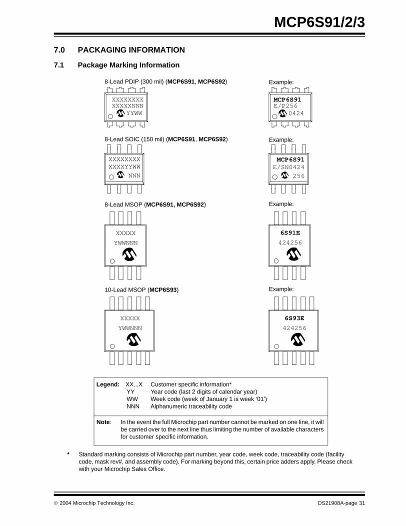
7.0 PACKAGING INFORMATION
7.1 Package Marking Information
XXXXXXXXXXXXXNNN
YYWW
8-Lead PDIP (300 mil) (MCP6S91, MCP6S92) Example:
8-Lead SOIC (150 mil) (MCP6S91, MCP6S92) Example:
XXXXXXXXXXXXYYWW
NNN
MCP6S91E/P256
0424
MCP6S91E/SN0424
256
8-Lead MSOP (MCP6S91, MCP6S92) Example:
XXXXX
YWWNNN
6S91E
424256
Legend: XX...X Customer specific information*YY Year code (last 2 digits of calendar year)WW Week code (week of January 1 is week ‘01’)NNN Alphanumeric traceability code
Note: In the event the full Microchip part number cannot be marked on one line, it will be carried over to the next line thus limiting the number of available characters for customer specific information.
* Standard marking consists of Microchip part number, year code, week code, traceability code (facility code, mask rev#, and assembly code). For marking beyond this, certain price adders apply. Please check with your Microchip Sales Office.
10-Lead MSOP (MCP6S93) Example:
XXXXX
YWWNNN
6S93E
424256
2004 Microchip Technology Inc. DS21908A-page 31

MCP6S91/2/3
8-Lead Plastic Dual In-line (P) – 300 mil (PDIP)
B1
B
A1
A
L
A2
p
α
E
eB
β
c
E1
n
D
1
2
Units INCHES* MILLIMETERSDimension Limits MIN NOM MAX MIN NOM MAX
Number of Pins n 8 8Pitch p .100 2.54Top to Seating Plane A .140 .155 .170 3.56 3.94 4.32Molded Package Thickness A2 .115 .130 .145 2.92 3.30 3.68Base to Seating Plane A1 .015 0.38Shoulder to Shoulder Width E .300 .313 .325 7.62 7.94 8.26Molded Package Width E1 .240 .250 .260 6.10 6.35 6.60Overall Length D .360 .373 .385 9.14 9.46 9.78Tip to Seating Plane L .125 .130 .135 3.18 3.30 3.43Lead Thickness c .008 .012 .015 0.20 0.29 0.38Upper Lead Width B1 .045 .058 .070 1.14 1.46 1.78Lower Lead Width B .014 .018 .022 0.36 0.46 0.56Overall Row Spacing § eB .310 .370 .430 7.87 9.40 10.92Mold Draft Angle Top α 5 10 15 5 10 15Mold Draft Angle Bottom β 5 10 15 5 10 15* Controlling Parameter
Notes:Dimensions D and E1 do not include mold flash or protrusions. Mold flash or protrusions shall not exceed
JEDEC Equivalent: MS-001Drawing No. C04-018
.010” (0.254mm) per side.
§ Significant Characteristic
2004 Microchip Technology Inc. DS21908A-page 32

MCP6S91/2/3
8-Lead Plastic Small Outline (SN) – Narrow, 150 mil (SOIC)
Foot Angle φ 0 4 8 0 4 8
1512015120βMold Draft Angle Bottom1512015120αMold Draft Angle Top
0.510.420.33.020.017.013BLead Width0.250.230.20.010.009.008cLead Thickness
0.760.620.48.030.025.019LFoot Length0.510.380.25.020.015.010hChamfer Distance5.004.904.80.197.193.189DOverall Length3.993.913.71.157.154.146E1Molded Package Width6.206.025.79.244.237.228EOverall Width0.250.180.10.010.007.004A1Standoff §1.551.421.32.061.056.052A2Molded Package Thickness1.751.551.35.069.061.053AOverall Height
1.27.050pPitch88nNumber of Pins
MAXNOMMINMAXNOMMINDimension LimitsMILLIMETERSINCHES*Units
2
1
D
n
p
B
E
E1
h
Lβ
c
45°
φ
A2
α
A
A1
* Controlling Parameter
Notes:Dimensions D and E1 do not include mold flash or protrusions. Mold flash or protrusions shall not exceed .010” (0.254mm) per side.JEDEC Equivalent: MS-012Drawing No. C04-057
§ Significant Characteristic
2004 Microchip Technology Inc. DS21908A-page 33

MCP6S91/2/3
8-Lead Plastic Micro Small Outline Package (MS) (MSOP)
p
A
A1
A2
D
L
c
Dimensions D and E1 do not include mold flash or protrusions. Mold flash or protrusions shall not
.037.035FFootprint (Reference)
exceed .010" (0.254mm) per side.
Notes:
Drawing No. C04-111
*Controlling Parameter
Mold Draft Angle Top
Mold Draft Angle Bottom
Foot Angle
Lead Width
Lead Thickness
βα
c
B
φ
7
7
.004
.010
0
.006
.012
(F)
β
Dimension Limits
Overall Height
Molded Package Thickness
Molded Package Width
Overall Length
Foot Length
Standoff §
Overall Width
Number of Pins
Pitch
A
L
E1
D
A1
E
A2
.016
.114
.114
.022
.118
.118
.002
.030
.193
.034
MIN
p
n
Units
.026
NOM
8
INCHES
1.000.950.90.039
0.15
0.30
.008
.016
6
0.10
0.25
0
7
7
0.20
0.40
6
MILLIMETERS*
0.65
0.86
3.00
3.00
0.55
4.90
.044
.122
.028
.122
.038
.006
0.40
2.90
2.90
0.05
0.76
MINMAX NOM
1.18
0.70
3.10
3.10
0.15
0.97
MAX
8
α
E1
E
Bn 1
2
φ
§ Significant Characteristic
.184 .200 4.67 .5.08
2004 Microchip Technology Inc. DS21908A-page 34

MCP6S91/2/3
10-Lead Plastic Micro Small Outline Package (MS) (MSOP)
Dimensions D and E1 do not include mold flash or protrusions. Mold flash or protrusions shall not
.037 REFFFootprint
exceed .010" (0.254mm) per side.
Notes:
Drawing No. C04-021
*Controlling Parameter
Mold Draft Angle Top
Mold Draft Angle Bottom
Foot Angle
Lead Width
Lead Thickness
βα
c
B
φ.003
.006
-
.009
Dimension Limits
Overall Height
Molded Package Thickness
Molded Package Width
Overall Length
Foot Length
Standoff
Overall Width
Number of Pins
Pitch
A
L
E1
D
A1
E
A2
.016 .024
.118 BSC
.118 BSC
.000
.030
.193 BSC
.033
MIN
p
n
Units
.020 TYP
NOM
10
INCHES
0.95 REF
-
0.23
.009
.012
0.08
0.15
-
-
0.23
0.30
MILLIMETERS*
0.50 TYP.
0.85
3.00 BSC
3.00 BSC
0.60
4.90 BSC
.043
.031
.037
.006
0.40
0.00
0.75
MINMAX NOM
1.10
0.80
0.15
0.95
MAX
10
5° 15°
5° 15°
-
- -
0° - 8°
5° -
5° -
15°
15°
JEDEC Equivalent: MO-187
8°0°
E
L
D
β
(F)
B
p
E1
n
φ
α
A2
1
2
c
A1
A
L1
--
- -
2004 Microchip Technology Inc. DS21908A-page 35

MCP6S91/2/3
NOTES:
2004 Microchip Technology Inc. DS21908A-page 36

MCP6S91/2/3
PRODUCT IDENTIFICATION SYSTEM
To order or obtain information, e.g., on pricing or delivery, refer to the factory or the listed sales office.
Sales and Support
Device: MCP6S91: One-channel PGAMCP6S91T: One-channel PGA
(Tape and Reel for SOIC and MSOP-8)MCP6S92: Two-channel PGAMCP6S92T: Two-channel PGA
(Tape and Reel for SOIC and MSOP-8)MCP6S93: Two-channel PGAMCP6S93T: Two-channel PGA
(Tape and Reel for MSOP-10)
Temperature Range: E = -40°C to +125°C
Package: MS = Plastic Micro Small Outline (MSOP), 8-leadP = Plastic DIP (300 mil Body), 8-leadSN = Plastic SOIC (150 mil Body), 8-leadUN = Plastic Micro Small Outline (MSOP), 10-lead
Examples:
a) MCP6S91-E/P: One-channel PGA, PDIP package.
b) MCP6S91-E/SN: One-channel PGA,SOIC package.
c) MCP6S91-E/MS: One-channel PGA,MSOP package.
a) MCP6S92-E/MS: Two-channel PGA,MSOP-8 package.
b) MCP6S92T-E/MS: Tape and Reel,Two-channel PGA,MSOP-8 package.
a) MCP6S93-E/UN: Two-channel PGA,MSOP-10 package.
b) MCP6S93T-E/UN: Tape and Reel,Two-channel PGA,MSOP-10 package.
PART NO. -X /XX
PackageTemperatureRange
Device
Data SheetsProducts supported by a preliminary Data Sheet may have an errata sheet describing minor operational differences and recommended workarounds. To determine if an errata sheet exists for a particular device, please contact one of the following:
1. Your local Microchip sales office2. The Microchip Corporate Literature Center U.S. FAX: (480) 792-72773. The Microchip Worldwide Site (www.microchip.com)
Please specify which device, revision of silicon and Data Sheet (include Literature #) you are using.
Customer Notification SystemRegister on our web site (www.microchip.com/cn) to receive the most current information on our products.
2004 Microchip Technology Inc. DS21908A-page 37
MCP6S91/2/3
NOTES:
DS21908A-page 38 2004 Microchip Technology Inc.

Note the following details of the code protection feature on Microchip devices:
• Microchip products meet the specification contained in their particular Microchip Data Sheet.
• Microchip believes that its family of products is one of the most secure families of its kind on the market today, when used in the intended manner and under normal conditions.
• There are dishonest and possibly illegal methods used to breach the code protection feature. All of these methods, to our knowledge, require using the Microchip products in a manner outside the operating specifications contained in Microchip’s Data Sheets. Most likely, the person doing so is engaged in theft of intellectual property.
• Microchip is willing to work with the customer who is concerned about the integrity of their code.
• Neither Microchip nor any other semiconductor manufacturer can guarantee the security of their code. Code protection does not mean that we are guaranteeing the product as “unbreakable.”
Code protection is constantly evolving. We at Microchip are committed to continuously improving the code protection features of ourproducts. Attempts to break Microchip’s code protection feature may be a violation of the Digital Millennium Copyright Act. If such actsallow unauthorized access to your software or other copyrighted work, you may have a right to sue for relief under that Act.
Information contained in this publication regarding deviceapplications and the like is provided only for your convenienceand may be superseded by updates. It is your responsibility toensure that your application meets with your specifications.MICROCHIP MAKES NO REPRESENTATIONS OR WAR-RANTIES OF ANY KIND WHETHER EXPRESS OR IMPLIED,WRITTEN OR ORAL, STATUTORY OR OTHERWISE,RELATED TO THE INFORMATION, INCLUDING BUT NOTLIMITED TO ITS CONDITION, QUALITY, PERFORMANCE,MERCHANTABILITY OR FITNESS FOR PURPOSE.Microchip disclaims all liability arising from this information andits use. Use of Microchip’s products as critical components inlife support systems is not authorized except with expresswritten approval by Microchip. No licenses are conveyed,implicitly or otherwise, under any Microchip intellectual propertyrights.
DS21908A-page 39
Trademarks
The Microchip name and logo, the Microchip logo, Accuron, dsPIC, KEELOQ, microID, MPLAB, PIC, PICmicro, PICSTART, PRO MATE, PowerSmart, rfPIC, and SmartShunt are registered trademarks of Microchip Technology Incorporated in the U.S.A. and other countries.
AmpLab, FilterLab, MXDEV, MXLAB, PICMASTER, SEEVAL, SmartSensor and The Embedded Control Solutions Company are registered trademarks of Microchip Technology Incorporated in the U.S.A.
Analog-for-the-Digital Age, Application Maestro, dsPICDEM, dsPICDEM.net, dsPICworks, ECAN, ECONOMONITOR, FanSense, FlexROM, fuzzyLAB, In-Circuit Serial Programming, ICSP, ICEPIC, Migratable Memory, MPASM, MPLIB, MPLINK, MPSIM, PICkit, PICDEM, PICDEM.net, PICLAB, PICtail, PowerCal, PowerInfo, PowerMate, PowerTool, rfLAB, rfPICDEM, Select Mode, Smart Serial, SmartTel and Total Endurance are trademarks of Microchip Technology Incorporated in the U.S.A. and other countries.
SQTP is a service mark of Microchip Technology Incorporated in the U.S.A.
All other trademarks mentioned herein are property of their respective companies.
© 2004, Microchip Technology Incorporated, Printed in the U.S.A., All Rights Reserved.
Printed on recycled paper.
2004 Microchip Technology Inc.
Microchip received ISO/TS-16949:2002 quality system certification for its worldwide headquarters, design and wafer fabrication facilities in Chandler and Tempe, Arizona and Mountain View, California in October 2003. The Company’s quality system processes and procedures are for its PICmicro® 8-bit MCUs, KEELOQ® code hopping devices, Serial EEPROMs, microperipherals, nonvolatile memory and analog products. In addition, Microchip’s quality system for the design and manufacture of development systems is ISO 9001:2000 certified.

DS21908A-page 40 2004 Microchip Technology Inc.
AMERICASCorporate Office2355 West Chandler Blvd.Chandler, AZ 85224-6199Tel: 480-792-7200 Fax: 480-792-7277Technical Support: http:\\support.microchip.comWeb Address: www.microchip.com
AtlantaAlpharetta, GA Tel: 770-640-0034 Fax: 770-640-0307
BostonWestford, MA Tel: 978-692-3848 Fax: 978-692-3821
ChicagoItasca, IL Tel: 630-285-0071 Fax: 630-285-0075
DallasAddison, TX Tel: 972-818-7423 Fax: 972-818-2924
DetroitFarmington Hills, MI Tel: 248-538-2250Fax: 248-538-2260
KokomoKokomo, IN Tel: 765-864-8360Fax: 765-864-8387
Los AngelesMission Viejo, CA Tel: 949-462-9523 Fax: 949-462-9608
San JoseMountain View, CA Tel: 650-215-1444Fax: 650-961-0286
TorontoMississauga, Ontario, CanadaTel: 905-673-0699 Fax: 905-673-6509
ASIA/PACIFICAustralia - SydneyTel: 61-2-9868-6733 Fax: 61-2-9868-6755
China - BeijingTel: 86-10-8528-2100 Fax: 86-10-8528-2104
China - ChengduTel: 86-28-8676-6200 Fax: 86-28-8676-6599
China - FuzhouTel: 86-591-750-3506 Fax: 86-591-750-3521
China - Hong Kong SARTel: 852-2401-1200 Fax: 852-2401-3431
China - ShanghaiTel: 86-21-5407-5533 Fax: 86-21-5407-5066China - ShenyangTel: 86-24-2334-2829Fax: 86-24-2334-2393
China - ShenzhenTel: 86-755-8203-2660 Fax: 86-755-8203-1760
China - ShundeTel: 86-757-2839-5507 Fax: 86-757-2839-5571
China - QingdaoTel: 86-532-502-7355 Fax: 86-532-502-7205
ASIA/PACIFICIndia - BangaloreTel: 91-80-2229-0061 Fax: 91-80-2229-0062
India - New DelhiTel: 91-11-5160-8632Fax: 91-11-5160-8632
Japan - KanagawaTel: 81-45-471- 6166 Fax: 81-45-471-6122
Korea - SeoulTel: 82-2-554-7200 Fax: 82-2-558-5932 or 82-2-558-5934
SingaporeTel: 65-6334-8870 Fax: 65-6334-8850
Taiwan - KaohsiungTel: 886-7-536-4818Fax: 886-7-536-4803
Taiwan - TaipeiTel: 886-2-2500-6610 Fax: 886-2-2508-0102
Taiwan - HsinchuTel: 886-3-572-9526Fax: 886-3-572-6459
EUROPEAustria - WeisTel: 43-7242-2244-399Fax: 43-7242-2244-393Denmark - BallerupTel: 45-4420-9895 Fax: 45-4420-9910
France - MassyTel: 33-1-69-53-63-20 Fax: 33-1-69-30-90-79
Germany - IsmaningTel: 49-89-627-144-0 Fax: 49-89-627-144-44
Italy - Milan Tel: 39-0331-742611 Fax: 39-0331-466781
Netherlands - DrunenTel: 31-416-690399 Fax: 31-416-690340
England - BerkshireTel: 44-118-921-5869Fax: 44-118-921-5820
WORLDWIDE SALES AND SERVICE
09/27/04