single-chip voice record/playback devices 16-...
TRANSCRIPT

1
®
FEATURES
• Easy-to-use single-chip voice Record/Play-back solution
• High-quality, natural voice/audio reproduction
• Fully addressable to handle multiple messages
• 100-year message retention (typical)
100,000 record cycles (typical)
On-chip clock source
ISD1000A Series
Single-Chip Voice Record/Playback Devices16- and 20-Second Durations
06.DataBook_1000A Dsht Page 1 Friday, September 27, 1996 10:44 AM
• Manual switch or microcontroller compatible– Playback can be edge- or level-
activated
•
•
•
• Single-chip durations of 16 and 20 seconds
• Directly cascadable for longer durations
• Power-down mode– 1 µA standby current (typical)
• Zero-power message storage– Eliminates battery backup circuits
•
•
•
Information Storage Devices, Inc.
ISD1000A SERIES SUMMARY
PartNumber
Duration(Seconds)
ISD1016A 16
ISD1020A 20
No algorithm development required
Single +5 volt supply
Available in die form, DIP, and SOIC packaging
Industrial temperature (-40°C to +85°C) version available
1–1
Input SampleRate (KHz)
Typical Filter Pass Band
(KHz)
8 3.4
6.4 2.7

Product Data Sheets
ISD1000A Series
-1
GENERAL DESCRIPTION
Information Storage Devices’ ISD1000A Chip-Corder
®
Series provides high-quality, single-chiprecord/playback solutions for 16- and 20-secondmessaging applications. The CMOS devices
DETAILED DESCRIPTION
The ISD1000A ChipCorder Series devices aredesigned to Record and Play back audio andvoice information in a single chip with a minimumof circuit complexity. This compact, easy-to-use,
06.DataBook_1000A Dsht Page 2 Friday, September 27, 1996 10:44 AM
include an on-chip oscillator, microphone pream-plifier, automatic gain control, antialiasing filter,smoothing filter, and speaker amplifier. In addi-tion, the ISD1000A Series is fully microprocessor-compatible, allowing complex messaging andaddressing to be achieved.
Recordings are stored in on-chip nonvolatilememory cells, providing zero-power messagestorage. This unique, single-chip solution is madepossible through ISD's patented multilevel stor-age technology. Voice and audio signals arestored directly into memory in their natural form,providing high-quality, solid-state voice reproduc-tion.
ISD1000A SERIES BLOCK DIAGRAM
1–2
Amp
TimingInternal Clock
Pre- Amp
VCCA VCCD
Power Conditioning
A0 A2 A3 A4 A5 A
Address Buffers
ANA IN
ANA OUT
MIC
MIC REF
AGC
Ana
Dec
oder
s
Mu
SXCLK
VSSA VSSD A1
Automatic Gain Control
(AGC)
5-Pole Active Antialiasing Filter
nonvolatile, low-power solution has been madepossible by ISD's multilevel storage technology —a breakthrough in storage technology in EEPROM.ISD’s multilevel storage technology results in stor-age density that is eight times greater than digitalmemory. The ISD1000A nonvolatile analog arrayconsists of 128K cells — the equivalent of 1 Mbitsof digital storage.
The ISD1000A Series eliminates the need for dig-ital conversion, digital compression, and voicesynthesis techniques which often compromisevoice quality and are more complicated to use.The ISD1000A Series includes signal conditioningcircuits and control functions which enable a com-plete, high-quality Recording and Playback sys-tem in a single device. The ISD1000A is availablein two versions, which store voice in 16- or 20-sec-ond arrays. Additional devices may be cascaded
A76
log Transceivers
128 K Cell Nonvolatile ltilevel Storage
Array Amp
ampling Clock
PD P/R CE EOM
Device Control
AUX IN
SP+
SP–Mux
5-Pole Active Smoothing Filter
R

Product Data Sheets
ISD1000A Series
1
to achieve longer recording durations. The non-volatile storage array is based on production-proven, low-power CMOS EEPROM technology.
The highly integrated ISD1000A Series containsall the basic functions required for high-quality
assures the lowest possible overall power con-sumption.
On-chip control functions make the ISD1000ASeries very easy to use in a wide array of applica-tions. Each device offers a variety of operating
SSD
SSA
M0/A0 M1/A1 M2/A2 M3/A3 M4/A4 M5/A5
NC NC A6 A7
AUX IN V V SP+
V P/R XCLK EOM PD CE NC ANA OUT ANA IN AGC MIC REF MIC V SP–
CCD
CCA
DIP/SOIC
1
2
3
4
5
6
7
8
9
10
11
12
13
14
28
27
26
25
24
23
22
21
20
19
18
17
16
15
ISD1000A SERIES PINOUTS
06.DataBook_1000A Dsht Page 3 Friday, September 27, 1996 10:44 AM
voice Recording and Playback. The noise-cancel-ling Microphone Preamplifier and Automatic GainControl (AGC) record both low-volume and high-volume sounds. The AGC attack and releasetimes are adjusted by an external resistor andcapacitor. Antialiasing is performed by a continu-ous fifth-order Chebyshev filter, requiring no exter-nal components or clocks to give toll-qualityreproduction. The low corner of the passband isuser-settable by two external capacitors. Thedevices contain their own temperature-stabilizedtimebase oscillator.
The ISD1000A devices drive a speaker directlythrough differential outputs. This boosts power byfour times and eliminates the need for a seriescapacitor or an output amplifier. The device willoperate from a single power supply or from batter-ies. The device also includes a power down func-tion for applications where minimum powerconsumption is critical. The CMOS-based design,combined with the nonvolatile storage array,
1–3
modes and interface options. The devices may beused in applications that require little more than afew switches and a battery. The devices may alsobe integrated into electronic systems where digitaladdresses can be provided for more sophisti-cated message addressing and control. TheISD1000A array is organized into 160 segments.Addresses A0 through A7 provide access to eachsegment in the array for message addressing.Addressing provides the capability of construct-ing messages by combining stored phrases andsounds.
PIN DESCRIPTIONS
Voltage Inputs (VCCA, VCCD)
To minimize noise, the analog and digital circuitsin the ISD1000A Series devices use separatepower busses. These voltage busses are broughtout to separate pins and should be tied togetheras close to the supply as possible. In addition,these supplies should be decoupled as close tothe package as possible.
Ground Inputs (VSSA, VSSD)
The ISD1000A Series of devices utilizes separateanalog and digital ground busses. These pinsshould be tied together as close to the packageas possible and connected through a low-imped-ance path to power supply ground.
Power Down Input (PD)When not recording or playing back, the PD pinshould be pulled HIGH to place the part in a verylow power mode (see ISB specification). WhenEOM pulses LOW for an overflow condition, PDshould be brought HIGH to reset the addresspointer back to the beginning of the Record/Play-back space.

Product Data Sheets
ISD1000A Series
-1
Chip Enable Input (CE)
The CE pin is taken LOW to enable all Playbackand Record operations. The address inputs andPlayback/Record input (P/R) are latched by thefalling edge of CE. When CE is taken HIGH, the
Microphone Input (MIC)
The microphone input transfers its signal to theon-chip preamplifier. An on-chip Automatic GainControl (AGC) circuit controls the gain of thispreamplifier from -15 to 24 dB. An external micro-
06.DataBook_1000A Dsht Page 4 Friday, September 27, 1996 10:44 AM
1–4
ISD1000A is unselected, the P/R is HIGH, and theauxiliary input is directed into the speaker ampli-fier.
Playback/Record Input (P/R)The P/R input is latched by the falling edge of theCE pin. A HIGH level selects a Playback cyclewhile a LOW level selects a Record cycle. For aRecord cycle, the address inputs provide thestarting address and recording continues until PDor CE is pulled HIGH or an overflow is detected(i.e. the chip is full). When a Record cycle is termi-nated by pulling PD or CE HIGH, an End-Of-Mes-sage (EOM) marker is stored at the currentaddress in memory. For a Playback cycle, theaddress inputs provide the starting address andthe device will play until an EOM marker isencountered. The device can continue past anEOM marker in an operational mode, or if CE isheld LOW in address mode. (See page 1-6 formore Operational Modes).
End-Of-Message Output (EOM)A non-volatile marker is automatically inserted atthe end of each recorded message. It remainsthere until the message is recorded over. DuringPlayback, the EOM output pulses LOW for aperiod of TEOM at the end of each message, or inthe event of a message overflow (device full).
In addition, the ISD1000A Series has an internalVCC detect circuit to maintain message integrityshould VCC fall below 3.5V. In this case, EOMgoes LOW and the device is fixed in Playback-only mode. The EOM marker provides a conve-nient handshake signal for a processor, and alsofacilitates the cascading of devices.
phone should be AC coupled to this pin via aseries capacitor. The capacitor value, togetherwith the internal 10 Kohm resistance on this pin,determines the low-frequency cutoff for theISD1000A Series passband. See ISD’s Applica-tion Notes and Design Manual in this book foradditional information on low-frequency cutoff cal-culation.
Microphone Reference Input (MIC REF)The MIC REF input is the inverting input to themicrophone preamplifier. This provides a noise-canceling or common-mode rejection input to thedevice when connected to a differential micro-phone. IF THIS INPUT IS UNUSED, IT MUST BE LEFT
DISCONNECTED.
Automatic Gain Control Input (AGC)The AGC dynamically adjusts the gain of thepreamplifier to compensate for the wide range ofmicrophone input levels. The AGC allows the fullrange of whispers to loud sounds to be recordedwith minimal distortion. The “attack” time is deter-mined by the time constant of a 5 KΩ internalresistance and an external capacitor (C2) con-nected from the AGC pin to VSSA analog ground.The “release” time is determined by the time con-stant of an external resistor (R2) and an externalcapacitor (C2 on the schematic on page 1-17)connected in parallel between the AGC Pin andVSSA analog ground. Nominal values of 470 KΩand 4.7 µF give satisfactory results, in most cases.For AGC voltages of 1.5V and below, the pream-plifier is at its maximum gain of 24 dB. Reductionin preamplifier gain occurs for voltages of approx-imately 1.8V.

Product Data Sheets
ISD1000A Series
1
Analog Output (ANA OUT)
This pin provides the preamplifier output to theuser. The voltage gain of the preamplifier is deter-mined by the voltage level at the AGC pin. It has amaximum gain of about 24 dB for small input sig-
critical, as the clock is immediately divided bytwo.
IF
THE
XCLK
IS
NOT
USED
,
THIS
INPUT
MUST
BE
CONNECTED
TO
GROUND
.
Speaker Outputs (SP+/SP-)
06.DataBook_1000A Dsht Page 5 Friday, September 27, 1996 10:44 AM
1–5
nal levels.
Analog Input (ANA IN)The analog input pin transfers its signal to the chipfor recording. For microphone inputs, the ANAOUT pin should be connected via an externalcapacitor to the ANA IN pin. This capacitor value,together with the 2.7 KΩ input impedance of ANAIN, is selected to give additional cutoff at the low-frequency end of the voice passband. If thedesired input is derived from a source other thana microphone, the signal can be fed, capacitivelycoupled, into the ANA IN pin directly.
Optional External Clock Input (XCLK)ISD1000A devices are configured at the factorywith an internal sampling clock frequency cen-tered to ±1% of specification. The frequency ismaintained to a total variation of ±2.25% toler-ance over the entire commercial temperature and4.5 to 5.5 voltage ranges. The internal clock has a±5% tolerance over the industrial temperaturerange and 4.5 to 5.5 voltage range. A regulatedpower supply is recommended for industrial-tem-perature-range parts. If greater precision isrequired, the device can be clocked through theXCLK pin as follows.
These recommended clock rates should not bevaried because the antialiasing and smoothing fil-ters are fixed, and aliasing problems can occur ifthe sample rate differs from the one recom-mended. The duty cycle on the input clock is not
All devices in the ISD1000A Series include an on-chip differential speaker driver, capable of driving50 milliwatts into 16 Ω from AUX IN (12.2 mW frommemory).
The speaker outputs are held at VSSA levels duringrecord and power down. It is therefore not possi-ble to parallel speaker outputs of multipleISD1000A devices or the outputs of other speakerdrivers.
NOTEConnection of speaker outputs in parallelmay cause damage to the device.
While a single output may be used alone (includ-ing a coupling capacitor between the SP pin andthe speaker), these outputs may be used individ-ually with the output signal taken from either pin.Using the differential outputs results in a 4:1improvement in output power.
NOTENever ground or drive an output.
Auxiliary Input (AUX IN)The Auxiliary Input is multiplexed through to theoutput amplifier and speaker output pins when CEis HIGH and Playback has ended, or if the deviceis in overflow. When cascading multiple ISD1000Adevices, the AUX IN pin is used to connect a Play-back signal from a following device to theprevious output speaker drivers. For noise consid-erations, it is suggested that the Auxiliary Input notbe driven when the storage array is active.
Address/Mode Inputs (Ax/Mx)The Address/Mode Inputs provide two functions inthe ISD1000A Series: 1. Message address (either
PartNumber
Sample Rate Required Clock
ISD1016A 8.0 KHz 1024 KHz
ISD1020A 6.4 KHz 819.2 KHz

Product Data Sheets
ISD1000A Series
-1
A6 or A7 = LOW) and 2. ISD1000A Series Opera-tional Mode Options (A6 AND A7 = HIGH).
Operational mode options are shown in the Oper-ational Modes table. There are a maximum of 160message addresses (or segments). Each seg-
OPERATIONAL MODES
The ISD1000A Series is designed with severalbuilt-in operational modes provided to allow max-imum functionality with a minimum of additionalcomponents, described in detail below. The oper-
06.DataBook_1000A Dsht Page 6 Friday, September 27, 1996 10:44 AM
ment corresponds to one of 160 rows in the ana-log storage array. The message addresses(segments) are in locations 0 through 159 contig-uous. The playback/record duration of each seg-ment depends upon the device and is as follows:
An operation may be started at any address, asdefined by address pins A0-A7. Record or play-back continues with automatic incrementing of theinternal on-chip address until either CE is broughtHIGH (Record), an end of message marker isencountered (Playback with CE HIGH), or an over-flow (device full) condition results.
ational modes use the address pins on theISD1000A devices, but are mapped outside thevalid address range. When the two Most Signifi-cant Bits (MSBs) are HIGH (A6 = A7=1), theremaining address signals are interpreted asmode bits and NOT as address bits. Therefore,operational modes and direct addressing are notcompatible and cannot be used simultaneously.
There are two important considerations for usingoperational modes. First, all operations begin ini-tially at address 0, which is the beginning of theISD1000A address space. Later operations canbegin at other address locations, depending onthe operational mode(s) chosen. In addition, theaddress pointer is reset to 0 when the device ischanged from Record to Playback, or when aPower-Down cycle is executed.
Second, an Operational Mode is executed whenCE goes LOW and the two MSBs are HIGH. ThisOperational Mode remains in effect until the next
PartNumber
Segment Playback/Record Duration
ISD1016A 100 milliseconds
ISD1020A 125 milliseconds
Control Mode
Function Typical Use Jointly Compatible*
M0 Message cueing Fast-forward through messages M4, M5
OPERATIONAL MODES TABLE
1–6
M1 Delete EOM markers Position EOM marker at the end of the last message
M3, M4, M5
M2 Cascading Adding devices to extend message
M3 Looping Continuous playback from Address 0 M1, M5
M4 Consecutive addressing Record/Play multiple consecutive mes-sages
M0, M1, M5
M5 CE level-activated Allow message pausing M0, M1, M3, M4
NOTE: An asterisk (*) indicates additional operational modes which can be used simultaneously with the given mode.

Product Data Sheets
ISD1000A Series
1
LOW-going CE signal, at which point the currentaddress/mode levels are sampled and executed.
NOTE
The two MSBs are on pins 9 and 10 for
each ISD1000A Series member.
M2 — Used for Cascading
During playback, EOM goes LOW at array over-flow only. Normal EOM pulses are turned off.
M3 — Message Looping
06.DataBook_1000A Dsht Page 7 Friday, September 27, 1996 10:44 AM
OPERATIONAL MODES DESCRIPTIONThe Operational Modes can be used in conjunc-tion with a microcontroller, or they can be hard-wired to provide the desired system operation.
M0 — Message CueingMessage Cueing allows the user to skip throughmessages, without knowing the actual physicaladdresses of each message. Each CE LOWpulse causes the internal address pointer to skipto the next message. This mode should be usedfor Playback only, and is typically used with theM4 Operational Mode.
M1 — Delete EOM MarkersThe M1 Operational Mode allows sequentiallyrecorded messages to be combined into a singlemessage with only one EOM marker set at the endof the combined message. When this operationalmode is configured, messages recorded sequen-tially are played back as one continuous mes-sage.
The M3 Operational Mode allows for the auto-matic, continuously repeated playback of themessage located at the beginning of the addressspace. A message CANNOT completely fill theISD1000A device and loop.
M4 — Consecutive AddressingDuring normal operations, the address pointer willreset when a message is played through to anEOM marker. The M4 Operational Mode inhibitsthe address pointer reset on EOM, allowing mes-sages to be played back consecutively.
M5 — CE Level ActivatedThe default mode for ISD1000A devices is for CEto be edge-activated on Playback and level-acti-vated on Record. The M5 Operational Modecauses the CE pin to be interpreted as level-acti-vated as opposed to edge-activated during Play-back. This is specifically useful for terminatingPlayback operations using the CE signal. In thismode, CE LOW begins a Playback cycle at thebeginning of device memory.
1–7
1–8
Product Data Sheets
ISD1000A Series
-1
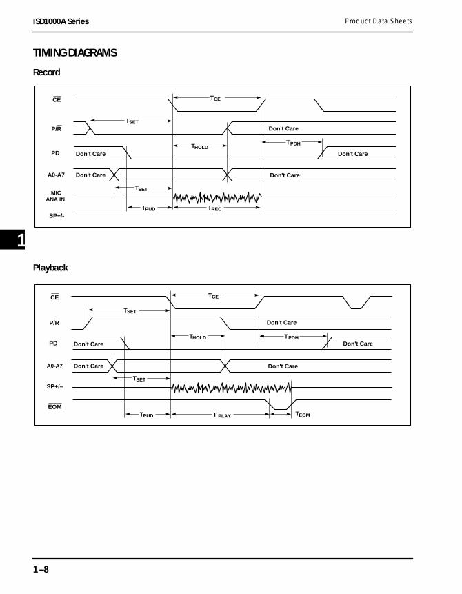
TIMING DIAGRAMS
Record
Playback
A0-A7
CE
MicAna In
TCE
TPDH
TSET
THOLD
SP+/-
PD
TPUD
Don't Care
Don't Care
Don't Care
Don't Care
TSET
P/R
TREC
Don't Care
A0-A9
CE
TCE
TSET
THOLDPD
SP+/–
EOMTPUD TEOM
Don't Care
Don't Care
Don't Care
Don't Care
TSET
P/R
TPDH
T PLAY
Don't Care
MICANA IN
A0-A7
06.DataBook_1000A Dsht Page 8 Friday, September 27, 1996 10:44 AM

Product Data SheetsISD1000A Series
1
ABSOLUTE MAXIMUM RATINGS (PACKAGED PARTS)
Condition Value
OPERATING CONDITIONS (PACKAGED PARTS)
Condition Value
Typ (1) Max(2) Units Conditions
06.DataBook_1000A Dsht Page 9 Friday, September 27, 1996 10:44 AM
NOTE: Stresses above those listed may cause permanent damage to the device. Exposure to the absolute maximum ratings may affect device reliability. Functional operation is not implied at these conditions.
Junction temperature 150° C
Storage temperature range –65° C to +150° C
Voltage applied to any pin (VSS – 0.3 V) to (VCC + 0.3 V)
Voltage applied to any pin (Input current limited to ± 20 mA)
(VSS – 1.0 V) to (VCC + 1.0 V)
Lead temperature (soldering – 10 seconds)
300° C
VCC - VSS – 0.3 V to + 7.0 V
DC PARAMETERS (PACKAGED PARTS)
Symbol Parameters Min(2)
VIL Input Low Voltage
NOTES: 1. Case temperature.2. VCC = VCCA = VCCD.3. VSS = VSSA = VSSD.
Commercial operating
temperature range(1)0° C to +70° C
Industrial operating
temperature(1)–40° C to +85° C
Supply voltage (VCC)(2) +4.5 V to +5.5 V
Ground voltage (VSS)(3) 0 V
0.8 V VCC = 4.5 V to 5.5 V
1–9
VIH Input High Voltage 2.0 V
VOL Output Low Voltage 0.4 V IOL = 4.0 mA
VOH Output High Voltage 2.4 V IOH = – 1.6 mA, VCC = 4.5 V to 5.5 V
VOH1 Output High Voltage VCC–0.4 V IOH = – 10 µA
ICC VCC Current (Operating) 25 30 mA REXT = ∞ (3)
ISB VCC Current (Standby) 1 10 µA (3)
IIL Input Leakage Current ±1 µA
REXT Output Load Impedance 16 Ω Speaker Load
RMIC Preamp In Input Resistance 10 KΩ Pins 17, 18
RAUX AUX Input Resistance 10 KΩ VCC = 4.5 V to 5.5 V

Product Data SheetsISD1000A Series
-1
RANA IN ANA IN Input Resistance 3.0 KΩ
APRE1 Preamp Gain 1 24 dB AGC = 0.0 V, VCC = 4.5 V to 5.5 V
S
F
F
T
T
T
T
T
T
Symbol Parameters Min(2) Typ (1) Max(2) Units Conditions
DC PARAMETERS (PACKAGED PARTS) – CONTINUED
06.DataBook_1000A Dsht Page 10 Friday, September 27, 1996 10:44 AM
1–10
NOTES: 1. Typical values @ TA = 25° C and 5.0 V.2. All Min/Max limits are guaranteed by ISD via electrical testing or characterization.
Not all specifications are 100% tested. 3. VCCA and VCCD connected together.
AC PARAMETERS (PACKAGED PARTS)
APRE2 Preamp Gain 2 – 45 15 dB AGC = 2.5 V
AAUX AUX IN/ SP+ Gain 0.9 V/V VCC = 4.5 V to 5.5 V
AARP ANA IN to SP+/- Gain 22 dB
RAGC AGC Output Resistance 5 KΩ
IPREH Preamp Out Source – 1 mA @ VOUT = 1.0 V, VCC = 4.5 V to 5.5 V
IPREL Preamp In Sink 0.8 mA @ VOUT = 2.0 V, VCC = 4.5 V to 5.5 V
ymbol Characteristic Min(2) Typ (1) Max(2) Units Conditions
S Internal Clock — ISD1016ASampling Frequency — ISD1020A
86.4
KHzKHz
(9)(9)
CF Filter Pass Band — ISD1016A— ISD1020A
3.42.7
KHzKHz
3 dB Roll-Off Point(3)(10)
3 dB Roll-Off Point(3)(10)
REC Record Duration — ISD1016A— ISD1020A
1620
secsec
PLAY Playback Duration — ISD1016A— ISD1020A
1620
secsec
(9)(9)
CE CE Pulse Width — ISD1016A— ISD1020A
100100
nsecnsec
SET Control/Address Setup Time — ISD1016A— ISD1020A
300300
nsecnsec
HOLD Control/Address Hold Time — ISD1016A— ISD1020A
00
nsecnsec
PUD Power-Up Delay — ISD1016A— ISD1020A
18.7531.25
msecmsec

Product Data Sheets ISD1000A Series
1
TPDR PD Pulse Width - Record — ISD1016A— ISD1020A
2531.25
msecmsec
(6)(6)
TPDP PD Pulse Width - Play — ISD1016A 12.5 msec (7)
T
T
T
T
P
V
V
V
V
Symbol Characteristic Min(2) Typ (1) Max(2) Units Conditions
AC PARAMETERS (PACKAGED PARTS) – CONTINUED
06.DataBook_1000A Dsht Page 11 Friday, September 27, 1996 10:44 AM
1–11
NOTES: 1. Typical values @ TA = 25° C and 5.0 V.2. All Min/Max limits are guaranteed by ISD via electrical testing or characterization. Not all specifications are 100% tested. 3. Low-frequency cutoff depends upon value of external capacitors (see Pin Descriptions).4. From AUX IN; if ANA IN is driven at 50 mV p-p, the POUT= 12.2 mW, typical.5. With 5.1 KΩ series resistor at ANA IN.6. This is the minimum pulse width required to guarantee that a Record cycle will be interrupted. A LOW-going PD pulse
of less than this interval during Record may be ignored. 7. This is the minimum pulse width required to guarantee that a Playback cycle will be interrupted. A LOW-going PD pulse
of less than this interval during Playback may be ignored. 8. This is the minimum pulse width required to reset the device when in a static condition; i.e., not actively recording or
playing back. 9. Sampling Frequency and Playback Duration will vary as much as ±2.25% over the commercial temperature and voltage
range and ±5% over the industrial temperature and voltage range. For greater stability, an external clock can be utilized (see Pin Descriptions).
10. Filter specification applies to the antialiasing filter and to the smoothing filter.
— ISD1020A 15.625 msec (7)
PDS PD Pulse Width - Static — ISD1016A— ISD1020A
100100
nsecnsec
(8)(8)
PDH Power Down Hold — ISD1016A— ISD1020A
00
nsecnsec
EOM EOM Pulse Width — ISD1016A— ISD1020A
12.515.6
msecmsec
HD Total Harmonic Distortion — ISD1016A— ISD1020A
11
%%
@ 1 KHz@ 1 KHz
OUT Speaker Output Power — ISD1016A
— ISD1020A
12.5
12.5
50
50
mW
mW
REXT = 16 Ω(4)
REXT = 16 Ω(4)
OUT Voltage Across Speaker Pins — ISD1016A— ISD1020A
2.52.5
V p–pV p–p
REXT = 600 ΩREXT = 600 Ω
IN1 MIC Input Voltage — ISD1016A— ISD1020A
2020
mVmV
Peak-to-Peak(5)
Peak-to-Peak(5)
IN2 ANA IN Input Voltage — ISD1016A— ISD1020A
5050
mVmV
Peak-to-PeakPeak-to-Peak
IN3 AUX IN Input Voltage — ISD1016A— ISD1020A
1.251.25
V p–pV p–p
REXT = 16 ΩREXT = 16 Ω

1–12
Product Data SheetsISD1000A Series
-1
TYPICAL PARAMETER VARIATION WITH VOLTAGE AND TEMPERATURE (PACKAGED PARTS)
-40
25
20
15
10
5
0
25 70 85
Op
erat
ing
Cu
rren
t (m
A)
Temperature (C)
-40 25 70 85
0.7
0.6
0.5
0.4
0.3
0.2
0.1
0
Sta
nd
by C
urr
ent
(µA
)
Temperature (C)
-40
1.5
1.0
0.5
0
-0.5
-1.0
-1.5
25 70 85
Per
cen
t C
han
ge
(%)
Temperature (C)
-40
0.6
0.5
0.4
0.3
0.2
0.1
0
25 70 85
Per
cen
t D
isto
rtio
n (
%)
Temperature (C)
TOTAL HARMONIC DISTORTION OSCILLATOR STABILITY
RECORD MODE OPERATING CURRENT (ICC) STANDBY CURRENT (ISB)
5.5 Volts 4.5 Volts
06.DataBook_1000A Dsht Page 12 Friday, September 27, 1996 10:44 AM

Product Data SheetsISD1000A Series
1
ABSOLUTE MAXIMUM RATINGS (DIE)
Condition Value
Junction temperature 150° C
OPERATING CONDITIONS (DIE)
Condition Value
Commercial operating 0° C to +50° C
0.8 V V = 4.5 V to 5.5 V
06.DataBook_1000A Dsht Page 13 Friday, September 27, 1996 10:44 AM
NOTE: Stresses above those listed may cause permanent damage to the device. Exposure to the absolute maximum ratings may affect device reliability. Functional operation is not implied at these conditions.
Storage temperature range –65° C to +150° C
Voltage applied to any pad (VSS – 0.3 V) to (VCC + 0.3 V)
Voltage applied to any pad(Input current limited to ±20 mA)
(VSS – 1.0 V) to (VCC + 1.0 V)
VCC - VSS – 0.3 V to + 7.0 V
DC PARAMETERS (DIE)
Symbol Parameters Min(2)
V Input Low Voltage
ILNOTES: 1. Case temperature.2. VCC = VCCA = VCCD.3. VSS = VSSA = VSSD.
temperature range (1)
Supply voltage (VCC)(2) +4.5 V to +6.5 V
Ground voltage (VSS)(3) 0 V
Typ(1) Max(2) Units Conditions
CC
1–13
VIH Input High Voltage 2.0 V
VOL Output Low Voltage 0.4 V IOL = 4.0 mA
VOH Output High Voltage 2.4 V IOH = –1.6 mA, VCC = 4.5 V to 5.5 V
VOH1 Output High Voltage VCC–0.4 V IOH = – 10 µA
ICC VCC Current (Operating) 25 30 mA REXT = ∞ (3)
ISB VCC Current (Standby) 1 10 µA (3)
IIL Input Leakage Current ±1 µA
REXT Output Load Impedance 16 Ω Speaker Load
RMIC Preamp In Input Resistance 10 KΩ Pins 17, 18
RAUX AUX Input Resistance 10 KΩ VCC = 4.5 V to 5.5 V
RANA IN ANA IN Input Resistance 3.0 KΩ

Product Data SheetsISD1000A Series
-1
APRE1 Preamp Gain 1 24 dB AGC = 0.0 V, VCC = 4.5 V to 5.5 V
APRE2 Preamp Gain 2 – 45 15 dB AGC = 2.5 V
S
F
F
T
T
T
T
T
T
T
Symbol Parameters Min(2) Typ(1) Max(2) Units Conditions
DC PARAMETERS (DIE) – CONTINUED
06.DataBook_1000A Dsht Page 14 Friday, September 27, 1996 10:44 AM
1–14
NOTES: 1. Typical values @ TA = 25° C and 5.0 V.2. All Min/Max limits are guaranteed by ISD via electrical testing or characterization.
Not all specifications are 100% tested. 3. VCCA and VCCD connected together.
AC PARAMETERS (DIE)
AAUX AUX IN/ SP+ Gain 0.9 V/V VCC = 4.5 V to 5.5 V
AARP ANA IN to SP+/- Gain 22 dB
RAGC AGC Output Resistance 5 KΩ
IPREH Preamp Out Source – 1 mA @ VOUT = 1.0 V, VCC = 4.5 V to 5.5 V
IPREL Preamp In Sink 0.8 mA @ VOUT = 2.0 V, VCC = 4.5 V to 5.5 V
ymbol Characteristic Min(2) Typ (1) Max(2) Units Conditions
S Internal Clock — ISD1016ASampling Frequency — ISD1020A
86.4
KHzKHz
(9)(9)
CF Filter Pass Band — ISD1016A— ISD1020A
3.42.7
KHzKHz
3 dB Roll-Off Point(3)(10)
3 dB Roll-Off Point(3)(10)
REC Record Duration — ISD1016A— ISD1020A
1620
secsec
PLAY Playback Duration — ISD1016A— ISD1020A
1620
secsec
(9)(9)
CE CE Pulse Width — ISD1016A— ISD1020A
100100
nsecnsec
SET Control/Address Setup Time — ISD1016A— ISD1020A
300300
nsecnsec
HOLD Control/Address Hold Time — ISD1016A— ISD1020A
00
nsecnsec
PUD Power-Up Delay — ISD1016A— ISD1020A
18.7531.25
msecmsec
PDR PD Pulse Width - Record — ISD1016A— ISD1020A
2531.25
msecmsec
(6)(6)

Product Data SheetsISD1000A Series
1
TPDP PD Pulse Width - Play — ISD1016A— ISD1020A
12.515.625
msecmsec
(7)(7)
TPDS PD Pulse Width - Static — ISD1016A 100 nsec (8)
T
T
T
P
V
V
V
V
Symbol Characteristic Min(2) Typ (1) Max(2) Units Conditions
AC PARAMETERS (DIE) – CONTINUED
06.DataBook_1000A Dsht Page 15 Friday, September 27, 1996 10:44 AM
1–15
NOTES: 1. Typical values @ TA = 25° C and 5.0 V.2. All Min/Max limits are guaranteed by ISD via electrical testing or characterization.
Not all specifications are 100% tested. 3. Low-frequency cutoff depends upon value of external capacitors (see Pin Descriptions).4. From AUX IN; if ANA IN is driven at 50 mV p-p, the POUT= 12.2 mW, typical.5. With 5.1 KΩ series resistor at ANA IN.6. This is the minimum pulse width required to guarantee that a Record cycle will be interrupted. A LOW-going PD pulse
of less than this interval during Record may be ignored. 7. This is the minimum pulse width required to guarantee that a Playback cycle will be interrupted. A LOW-going PD pulse
of less than this interval during Playback may be ignored. 8. This is the minimum pulse width required to reset the device when in a static condition; i.e., not actively recording or
playing back. 9. Sampling frequency and Playback duration will vary as much as ±2.25% over the commercial temperature and voltage
range. For greater stability, an external clock can be utilized (see Pin Descriptions).10. Filter specification applies to the antialiasing filter and to the smoothing filter.
— ISD1020A 100 nsec (8)
PDH Power Down Hold — ISD1016A— ISD1020A
00
nsecnsec
EOM EOM Pulse Width — ISD1016A— ISD1020A
12.515.6
msecmsec
HD Total Harmonic Distortion — ISD1016A— ISD1020A
11
%%
@ 1 KHz@ 1 KHz
OUT Speaker Output Power — ISD1016A
— ISD1020A
12.5
12.5
50
50
mW
mW
REXT = 16 Ω(4)
REXT = 16 Ω(4)
OUT Voltage Across Speaker Pins — ISD1016A— ISD1020A
2.52.5
V p–pV p–p
REXT = 600 ΩREXT = 600 Ω
IN1 MIC Input Voltage — ISD1016A— ISD1020A
2020
mVmV
Peak-to-Peak(5)
Peak-to-Peak(5)
IN2 ANA IN Input Voltage — ISD1016A— ISD1020A
5050
mVmV
Peak-to-PeakPeak-to-Peak
IN3 AUX IN Input Voltage — ISD1016A— ISD1020A
1.251.25
V p–pV p–p
REXT = 16 ΩREXT = 16 Ω

1–16
Product Data SheetsISD1000A Series
-1
TYPICAL PARAMETER VARIATION WITH VOLTAGE AND TEMPERATURE (DIE)
0.5
0.4
0.3
0.2
0.1
0
0 25 50 0 25 50
-1.5
2.5
1.5
1.0
0.5
0
-0.5
-1.0
2.0
25
20
15
10
5
0
0 25 50 0 25 50
0
0.8
0.6
0.5
0.4
0.3
0.2
0.1
0.7
6.5 Volts 5.5 Volts 4.5 Volts
Op
erat
ing
Cu
rren
t (m
A)
Temperature (C)
Sta
nd
by C
urr
ent
(µA
)
Temperature (C)
Per
cen
t C
han
ge
(%)
Temperature (C)
Per
cen
t D
isto
rtio
n (
%)
Temperature (C)
TOTAL HARMONIC DISTORTION OSCILLATOR STABILITY
RECORD MODE OPERATING CURRENT (ICC) STANDBY CURRENT (ISB)
06.DataBook_1000A Dsht Page 16 Friday, September 27, 1996 10:44 AM

Product Data Sheets ISD1000A Series
1
SSD
SSA
A0 A1 A2 A3 A4 A5 A6 A7 CE PD P/R EOM XCLK
V V
V V
SP+ SP–
AUX IN ANA IN
ANA OUT
MIC REF
MIC AGC
CCD
CCA
C3
16 Ω SPEAKER
1
2
3
4
5
6
9
10
23
24
27
25
26
28
16
12
13
14
15
11
20
21
18
17
19
ELECTRET MICROPHONE
0.1 µF
CCVCCV
22 µF
SSV
PLAYBACK/RECORD
POWER DOWN
CHIP ENABLE
ISD1016A/1020A
0.1 µF0.1 µF
C5
0.1 µF Mic Ref
C10.1 µF
CCV
C24.7 µF
470 KΩR2 1 KΩ
R1
10 KΩR3
C4220 µF
(Note)
R5 5.1 KΩ
10 KΩR4
C7C6C8
APPLICATION EXAMPLE – DESIGN SCHEMATIC
APPLICATION EXAMPLE – BASIC DEVICE CONTROL
Control Step Function Action
1 Power up chip and select record/playback mode 1. PD = LOW
NOTE: If desired, pin 18 may be left unconnected (microphone preamplifier noise will be higher). In this case, pin 18 must not be tied to any other signal or voltage.Additional design example schematics are provided in the Application Notes and Design Manual in this book.
06.DataBook_1000A Dsht Page 17 Friday, September 27, 1996 10:44 AM
1–17
2. P/R = As desired
2 Set message address for record/playback Set addresses A0–A7
3 Begin playback/record CE = Pulsed LOW (Playback)CE = Held LOW (Record)
4 End cycle CE = HIGH and EOM reached
Product Data SheetsISD1000A Series
-1
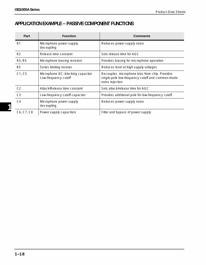
APPLICATION EXAMPLE – PASSIVE COMPONENT FUNCTIONS
Part Function Comments
R1 Microphone power supply Reduces power supply noise
06.DataBook_1000A Dsht Page 18 Friday, September 27, 1996 10:44 AM
decoupling
R2 Release time constant Sets release time for AGC
R3, R4 Microphone biasing resistors Provides biasing for microphone operation
R5 Series limiting resistor Reduces level at high supply voltages
C1, C5 Microphone DC–blocking capacitorLow-frequency cutoff
Decouples microphone bias from chip. Provides single-pole low-frequency cutoff and common-mode noise rejection
C2 Attack/Release time constant Sets attack/release time for AGC
C3 Low-frequency cutoff capacitor Provides additional pole for low-frequency cutoff
C4 Microphone power supply decoupling
Reduces power supply noise
C6, C7, C8 Power supply capacitors Filter and bypass of power supply
1–18

Product Data Sheets ISD1000A Series
ORDERING INFORMATION
Product Number Descriptor Key
06.DataBook_1000A Dsht Page 19 Friday, September 27, 1996 10:44 AM
ISD10 _ _ A _ _
1
ISD1000A Series
Duration:16 = 16 Seconds20 = 20 Seconds
Special Temperature Field:
Blank = Commercial Packaged (0˚C to +70˚C)or Commercial Die (0˚C to +50˚C)
I = Industrial (-40˚C to +85˚C)
Package Type:G = 28-Lead 0.350-Inch Small Outline Integrated Circuit
(SOIC)P = 28-Lead 0.600-Inch Plastic Dual In-Line Package
(PDIP)X = Die
Part Number Part Number
ISD1016AG ISD1020AG
ISD1016AGI ISD1020AGI
When ordering ISD1000A Series devices, please refer to the following valid part numbers.
ISD1016AP ISD1020AP
ISD1016API ISD1020API
ISD1016AX ISD1020AX
For the latest product information, access ISD’s worldwide website at http://www.isd.com.
1–19

1–20
Product Data SheetsISD1000A Series
-1
06.DataBook_1000A Dsht Page 20 Friday, September 27, 1996 10:44 AM