simple design consideration solar cell
TRANSCRIPT
Design Considerations Of Solar Cell
By
Anish Das
Roll no. -14MS60R16
MATERIALS SCIENCE CENTRE
Indian Institute of Technology
KHARAGPUR, 721302 - INDIA
FEBRUARY,2015107:35:44 PM
Overview
Designing of a solar cell
207:35:44 PM
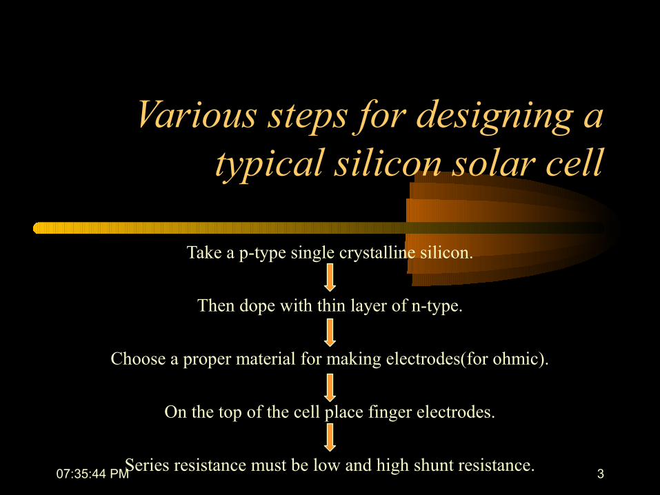
Various steps for designing a typical silicon solar cell
Take a p-type single crystalline silicon.
Then dope with thin layer of n-type.
Choose a proper material for making electrodes(for ohmic).
On the top of the cell place finger electrodes.
Series resistance must be low and high shunt resistance.307:35:44 PM
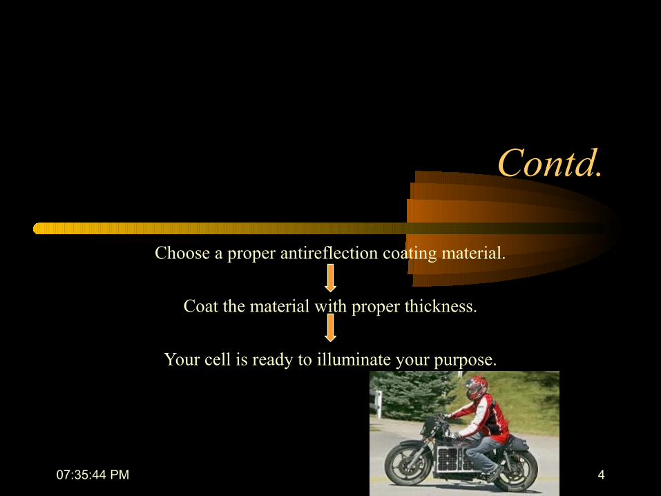
Contd.
Choose a proper antireflection coating material.
Coat the material with proper thickness.
Your cell is ready to illuminate your purpose.
407:35:44 PM
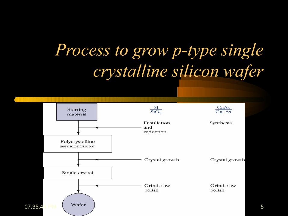
Process to grow p-type single crystalline silicon wafer
507:35:44 PM
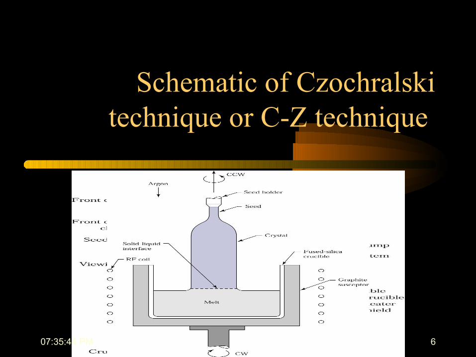
Schematic of Czochralski technique or C-Z technique
607:35:44 PM
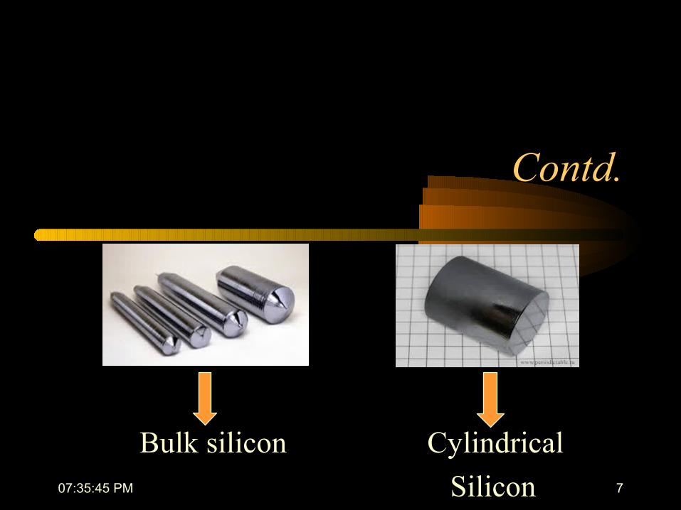
Contd.
Bulk silicon Cylindrical
Silicon 707:35:45 PM
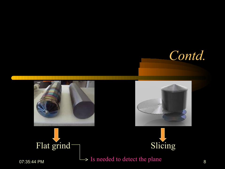
Contd.
Flat grind Slicing
Is needed to detect the plane
. .
807:35:44 PM
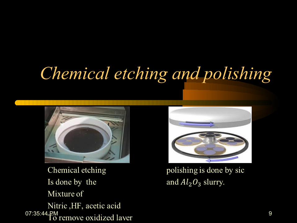
Chemical etching and polishing
907:35:44 PM
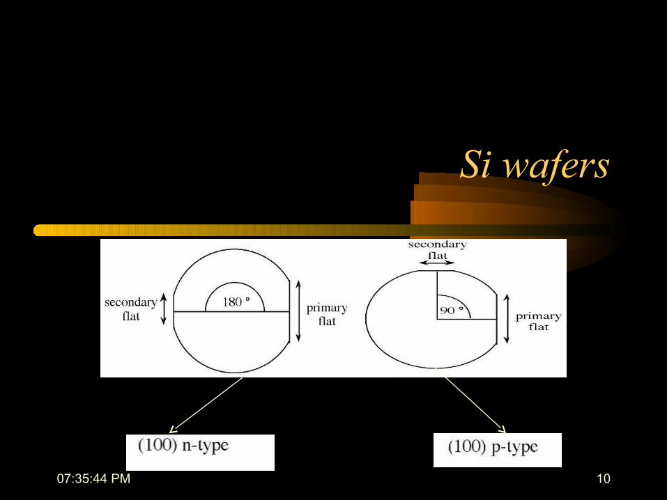
Si wafers
1007:35:44 PM
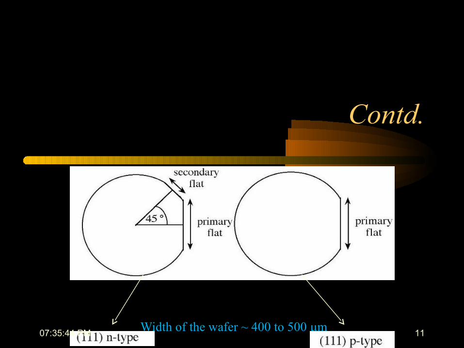
Contd.
Width of the wafer ~ 400 to 500 μm1107:35:44 PM
Doping of thin layer of n-type Si
1207:35:44 PM
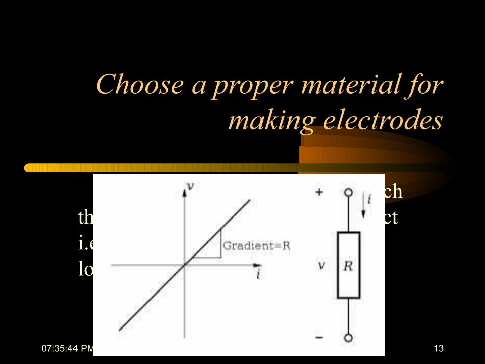
Choose a proper material for making electrodes
Electrode material must be such that it can easily make ohmic contact i.e. contact resistance must be very low.
1307:35:44 PM
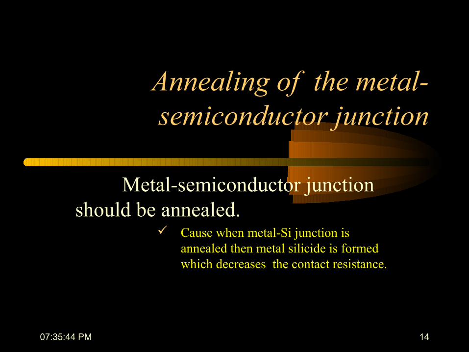
Annealing of the metal-semiconductor junction
Metal-semiconductor junction should be annealed.
Cause when metal-Si junction is annealed then metal silicide is formed which decreases the contact resistance.
1407:35:44 PM
Effect of resistance on solar cell
It reduces the solar cell efficiency. It reduces the fill factor of solar
cell.
1507:35:44 PM
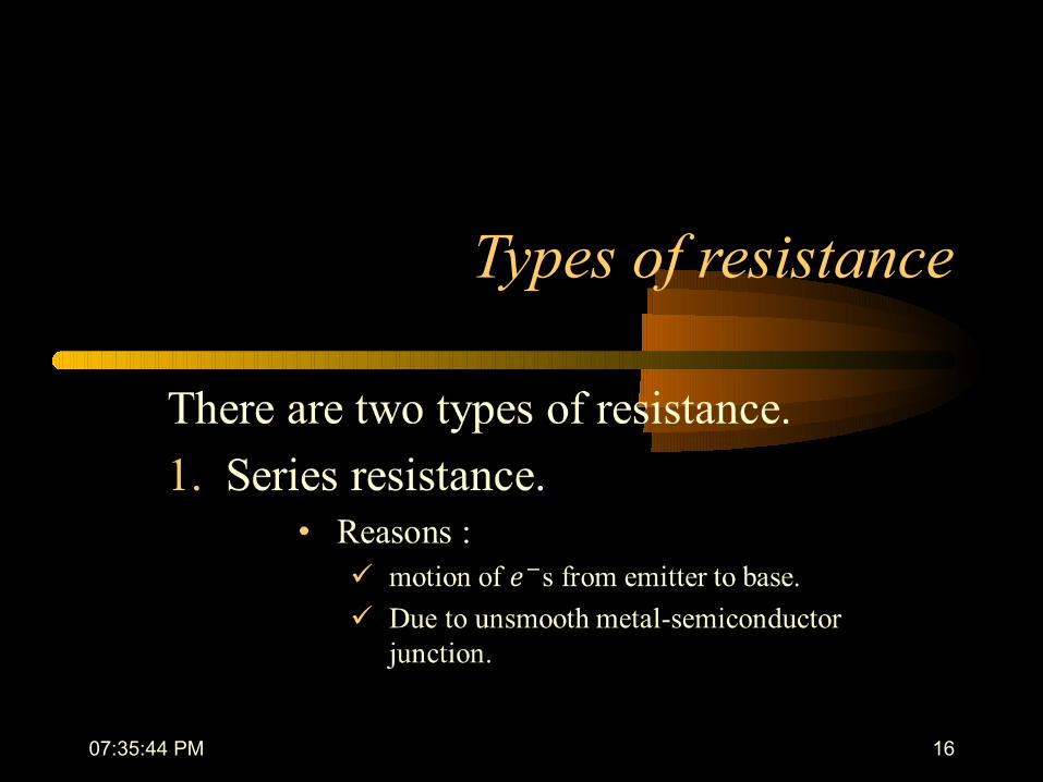
Types of resistance
1607:35:44 PM

Series resistance
1707:35:44 PM
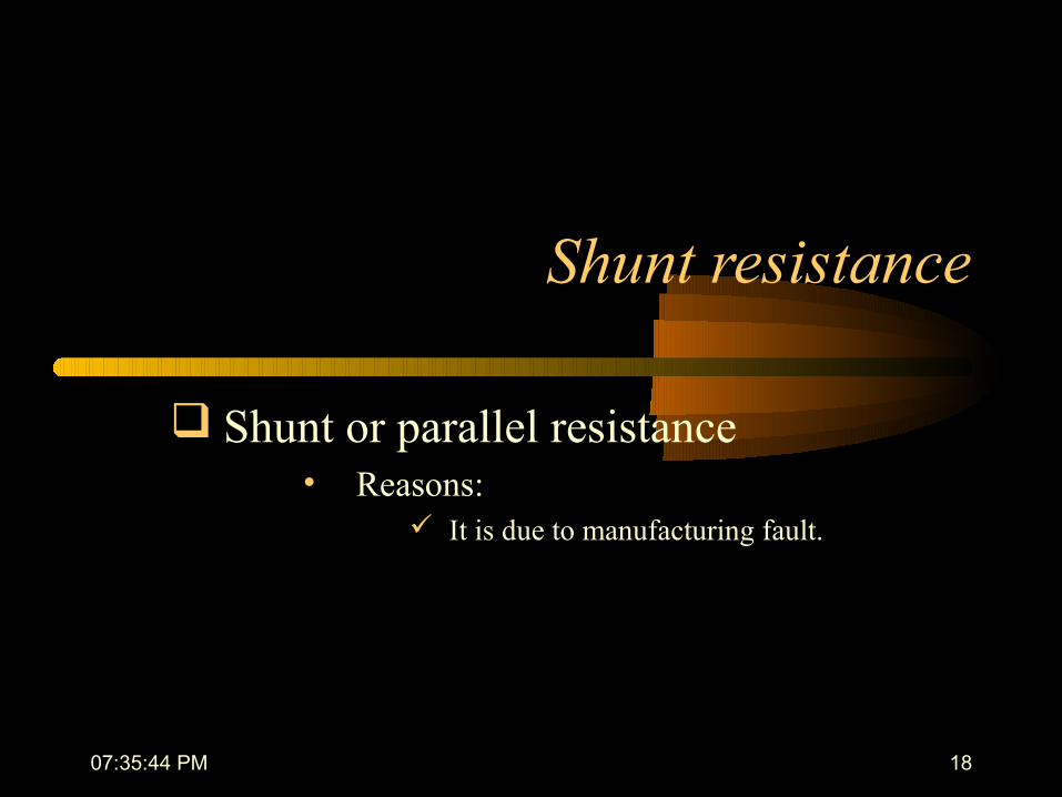
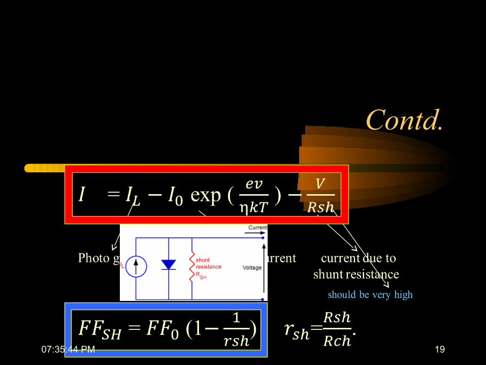
Shunt resistance
Shunt or parallel resistance• Reasons:
It is due to manufacturing fault.
1807:35:44 PM
Contd.
1907:35:44 PM
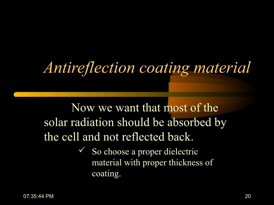
Antireflection coating material
Now we want that most of the solar radiation should be absorbed by the cell and not reflected back.
So choose a proper dielectric material with proper thickness of coating.
2007:35:44 PM
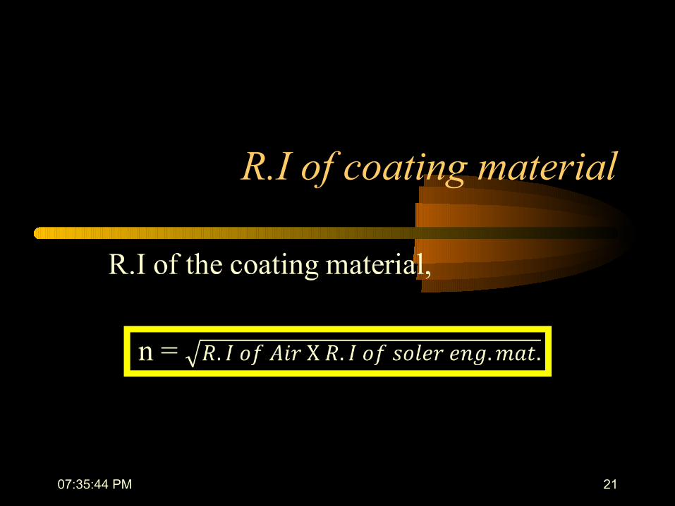
R.I of coating material
2107:35:44 PM
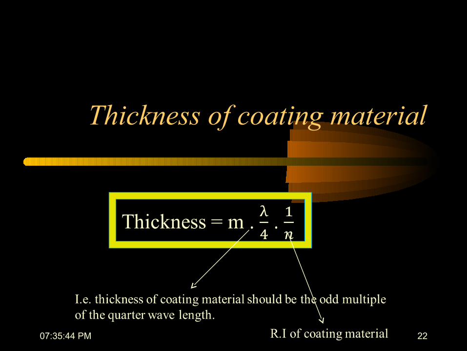
Thickness of coating material
2207:35:44 PM
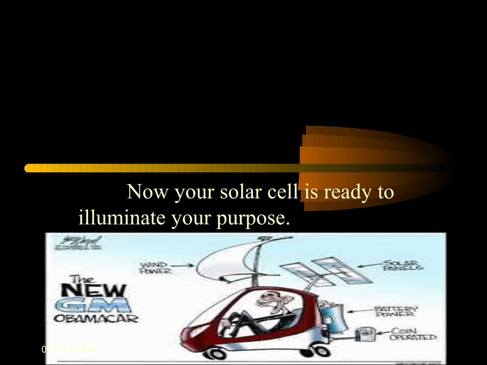
Now your solar cell is ready to illuminate your purpose.
2307:35:44 PM

The EndThe End
2407:35:44 PM
Any Question ?Any Question ?
2507:35:44 PM