silicon quantum integrated circuits: silicon-germanium … · 2019-09-24 ·...
TRANSCRIPT


NanoScience and Technology
NanoScience and Technology
Series Editors: P. Avouris B. Bhushan K. von Klitzing H. Sakaki R. Wiesendanger
The series NanoScience and Technology is focused on the fascinating nano-world, meso-scopic physics, analysis with atomic resolution, nano and quantum-effect devices, nano-mechanics and atomic-scale processes. All the basic aspects and technology-orienteddevelopments in this emerging discipline are covered by comprehensive and timely books.The series constitutes a survey of the relevant special topics, which are presented by leadingexperts in the field. These books will appeal to researchers, engineers, and advancedstudents.
Sliding FrictionPhysical Principles and ApplicationsBy B.N.J. Persson2nd Edition
Scanning Probe MicroscopyAnalytical MethodsEditor: R. Wiesendanger
Mesoscopic Physics and ElectronicsEditors: T. Ando, Y. Arakawa, K. Furuya,S. Komiyama, H. Nakashima
Biological Micro- and NanotribologyNature’s SolutionsBy M. Scherge and S.N. Gorb
Semiconductor Spintronicsand Quantum ComputationEditors: D.D. Awschalom, N. Samarth,D. Loss
Semiconductor Quantum DotsPhysics, Spectroscopy and ApplicationsEditors: Y. Masumoto and T. Takagahara
Nano-OptoelectonicsConcepts, Physics and DevicesEditor: M. Grundmann
Noncontact Atomic Force MicroscopyEditors: S. Morita, R. Wiesendanger,E. Meyer
NanoelectrodynamicsElectrons and Electromagnetic Fieldsin Nanometer-Scale StructuresEditor: H. Nejo
Single Organic NanoparticlesEditors: H. Masuhara, H. Nakanishi,K. Sasaki
Epitaxy of NanostructuresBy V.A. Shchukin, N.N. Ledentsov,D. Bimberg
Nanoscale Characterisationof Ferroelectric MaterialsScanning Probe Microscopy ApproachEditors: M. Alexe and A. Gruverman

E. Kasper D.J. Paul
Silicon QuantumIntegrated CircuitsSilicon–Germanium HeterostructureDevices: Basics and Realisations
With 263 Figures
123
Prof. Erich KasperInstitute of Semiconductor EngineeringUniversity of StuttgartPfaffenwaldring 4770569 Stuttgart, GermanyE-mail: [email protected]
Prof. D.J. PaulCavendish LaboratoryUniversity of CambridgeMadingley RoadCambridge CB3 0HE, UKE-mail: [email protected]
Series Editors:Professor Dr. Phaedon AvourisIBM Research Division, Nanometer Scale Science & TechnologyThomas J. Watson Research Center, P.O. Box 218Yorktown Heights, NY 10598, USA
Professor Dr. Bharat BhushanOhio State UniversityNanotribology Laboratory for Information Storage and MEMS/NEMS (NLIM)Suite 255, Ackerman Road 650, Columbus, Ohio 43210, USA
Professor Dr., Dres. h. c. Klaus von KlitzingMax-Planck-Institut fur Festkorperforschung, Heisenbergstrasse 170569 Stuttgart, Germany
Professor Hiroyuki SakakiUniversity of Tokyo, Institute of Industrial Science, 4-6-1 Komaba, Meguro-kuTokyo 153-8505, Japan
Professor Dr. Roland WiesendangerInstitut fur Angewandte Physik, Universitat Hamburg, Jungiusstrasse 1120355 Hamburg, Germany
Library of Congress Control Number: 2004116222
ISSN 1434-4904ISBN 3-540-22050-X Springer Berlin Heidelberg New York
This work is subject to copyright. All rights are reserved, whether thewholeor part of the material is concerned,specifically the rights of translation, reprinting, reuse of illustrations, recitation, broadcasting, reproductionon microfilm or in any other way, and storage in data banks. Duplication of this publication or parts thereof ispermitted only under the provisions of the German Copyright Law of September 9, 1965, in its current version,and permission for use must always be obtained from Springer. Violations are liable to prosecution under theGerman Copyright Law.
Springer is a part of Springer Science+Business Media.
springeronline.com
© Springer-Verlag Berlin Heidelberg 2005Printed in Germany
The use of general descriptive names, registered names, trademarks, etc. in this publication does not imply,even in the absence of a specific statement, that such names are exempt from the relevant protective laws andregulations and therefore free for general use.
Typesetting: Data conversion by the authors using a Springer TEX macro packageFinal processing by Frank Herweg, LeutershausenProduction: LE-TEX Jeloneck, Schmidt & Vöckler GbR, LeipzigCover design: design& production, Heidelberg
Printed on acid-free paper 57/3141/ - 5 4 3 2 1 0

Preface
For more than thirty years, progress in monolithic integration of transistorsinto integrated circuits (IC) has yielded an exponential growth of the per-formance and density of such circuits along with an exponential growth ofsales. In microelectronics this rapid and longstanding exponential growth isreferred to as Moore’s law after one of the pioneers of the integrated circuitindustry. The continuous shrinking of the lateral and vertical device dimen-sions is closely related to the increasing number of transistors on a chip, nowapproaching the tera scale (1012). The scaling of complementary metal-oxide–semiconductor (CMOS) technology is defined by the lateral lithography ruleswhich determine the future technology generations from the present 90 nmnode to the 65 nm, 45 nm, 30nm nodes and eventually down to some pointwhich will be the ultimate scalability of the technology (or the final eco-nomically viable technology node). Vertical dimensions in devices are often afactor of ten finer than the lateral dimensions defined by optical lithography,due to sophisticated deposition and epitaxy methods.
Quantum electronics, therefore, more than traditional microelectronicsfrequently relies on the vertical structure of the device, as the vertical dimen-sions can be controlled at the nanometre scale more easily. In this context adefinition of quantum electronics is required, because semiconductor physicsand its application in electronic devices are completely based on the law ofquantum mechanics. The transport and statistical behaviour of charged car-riers in semiconductors must be derived from the first principles of quantummechanics with statistical mechanics and are strongly influenced by the quan-tisation of charge and energy. Many of the basic semiconductor properties areuniquely defined by the quantum mechanics of the system. For instance theconcept of holes, which – through the Pauli exclusion principle – states thata missing valence band electron can be considered as a positive charged hole,the existence of a band gap which forbids electron states in an energy rangebetween the conduction band and valence band, and the effective mass ap-proximation, which treats carriers near their energy minimum as quasi-freewith masses differing from the free electron mass. The term quantum elec-tronics is frequently only used when artificial man-made structures are smallenough to allow the electronic or optical properties of devices to be stronglyinfluenced by quantum effects. In particular the lowering of the dimension-

Preface
ality of a structure results in a change of the density of states along withquantisation of electron states into subbands (when larger than the thermalsmearing (∼ kBT ) of the system) which may frequently completely changethe properties of devices. Typical structure dimensions for such quantisationin silicon with its relative large effective masses are below 10 to 20 nm. Fre-quently exploited quantum effects include the transmission of carriers throughbarriers (tunnelling), the bound states in quantum wells (quantisation) andthe mini-band formation in multi-quantum wells and superlattices (artificialsemiconductor). The general laws of quantum mechanics are the same for allsemiconductor materials. Why do we think that silicon quantum electron-ics is a topic worthy of a whole book? Silicon-based quantum electronics isprogressing in a significantly different way than for instance in group III/Vmaterials where many basic studies were completed and early successes wereobtained, e.g. with lasers and high electron mobility transistors (HEMTs).The reasons for the differences are related to the physics, the technology andthe economics. Silicon is an indirect semiconductor with six degenerate con-duction band valleys and the most important heterostructure SiGe/Si canbe used to separate electrons and holes to opposite sides of the heterointer-face (a so-called type II interface). A technologically stable heterostructurewith equal lattice constants (such as Ga As and GaAlAs) is not available ina silicon-based system. As a consequence the SiGe/Si heterostructures arestrained, giving additional freedom for material band structure designs butlimiting the usable thicknesses. The widespread dominance of silicon sub-strates in all areas of microelectronics offers enormous market opportunitiesfor quantum electronics, but also imposes strict manufacturing and operatingconditions especially concerning high complexity integration and room tem-perature operation. This book is organised around three main topics. The firstfew chapters review the methods and techniques for creating quantum struc-tures using combinations of heterostructures and conventional p/n-junctions;they also review the relevant semiconductor physics background (Chap. 3).Chapter 4 treats the influence of elastic strain on electronic structure and in-terface energies, in particular for the strained SiGe/Si system. Then followsa detailed discussion of devices, the examples having been selected by uswith respect to their potential for integration and also operation under roomtemperature conditions. The standard silicon p/n junctions, bipolar transis-tors and MOSFET devices are reviewed in Chap. 5. The SiGe hetero-bipolartransistor (HBT) is now a mainstream production technology following its in-troduction onto the market in 1999 and now dominates many high-frequencyapplications (Chap. 6). The hetero field-effect transistor (HFET) is enteringthe competition for future CMOS technology generations, offering a varietyof powerful solutions ranging from several tens of percent improvement tothe ultimate symmetric n- and p-channel transistors (Chap. 7). Tunnellingand optoelectronic phenomena (Chaps. 8, 9) could be the key to novel andrapidly expanding system-on-chip (SOC) solutions. The important question
vi

Preface
of possible integration techniques is investigated in Chap. 10. The reader isreferred to Chaps. 2, 3 and 5 when quick advice on materials science, technol-ogy, semiconductor physics and device principles is required. We have aimedthis text at two groups of readers but hope that both these and many otherswill benefit from this focused treatment. We hope that the many engineers in-volved in fueling the exponential progress in micro- and nanoelectronics willbe confronted with and increasingly utilise quantum effects. We also hopethat researchers in device physics and modelling, nanoelectronics and semi-conductor materials along with graduate students in electrical engineeringand computer science, physics and material science will come to see siliconas the model system for strained heterostructures. During the writing of thisbook certain chapters were used as a manuscript for the lecture “QuantumElectronics” in a graduate course “Electrical Engineering and InformationTechnology” at the University of Stuttgart. We thank the students for theircomments and are especially grateful for the help of the assistants GunterReitemann and Jens Werner.
E.KasperD.J. Paul
vii
Contents
1. Introduction . . . . . . . . . . . . . . . . . . . . . . . . . . . . . . . . . . . . . . . . . . . . . . 11.1 Microelectronics and Optoelectronics . . . . . . . . . . . . . . . . . . . . . . 31.2 From Microelectronics to Nanoelectronics . . . . . . . . . . . . . . . . . . 71.3 Self–ordering . . . . . . . . . . . . . . . . . . . . . . . . . . . . . . . . . . . . . . . . . . . 101.4 Further Reading . . . . . . . . . . . . . . . . . . . . . . . . . . . . . . . . . . . . . . . . 12
2. Material Science . . . . . . . . . . . . . . . . . . . . . . . . . . . . . . . . . . . . . . . . . . 132.1 Growth and Preparation Methods
(MBE, CVD, Implantation, Annealing) . . . . . . . . . . . . . . . . . . . . 132.2 Segregation and Diffusion of Dopants and Alloy Materials . . . 292.3 Lattice Mismatch and its Implication
on Critical Thickness and Interface Structure . . . . . . . . . . . . . . 352.4 Virtual Substrates and Strain Relaxation . . . . . . . . . . . . . . . . . . 402.5 Further Reading . . . . . . . . . . . . . . . . . . . . . . . . . . . . . . . . . . . . . . . . 47
3. Resume of Semiconductor Physics . . . . . . . . . . . . . . . . . . . . . . . 493.1 Quantum Mechanics . . . . . . . . . . . . . . . . . . . . . . . . . . . . . . . . . . . . 49
3.1.1 The Wave Behaviour of Particles . . . . . . . . . . . . . . . . . . . 493.1.2 The Potential Barrier
and Quantum Mechanical Tunnelling . . . . . . . . . . . . . . . 503.1.3 Quantum Wells . . . . . . . . . . . . . . . . . . . . . . . . . . . . . . . . . . 533.1.4 The Hydrogen Atom . . . . . . . . . . . . . . . . . . . . . . . . . . . . . 55
3.2 The Band Structure of Semiconductors . . . . . . . . . . . . . . . . . . . . 573.2.1 The Free Electron Picture and the Effective Mass . . . . 573.2.2 The Crystal Structure . . . . . . . . . . . . . . . . . . . . . . . . . . . . 593.2.3 Bloch’s Theorem and Bloch Functions . . . . . . . . . . . . . . 613.2.4 The Kronig-Penney Model . . . . . . . . . . . . . . . . . . . . . . . . 613.2.5 The Tight Binding Model . . . . . . . . . . . . . . . . . . . . . . . . . 643.2.6 Pseudopotentials and k.p Theory . . . . . . . . . . . . . . . . . . 683.2.7 Bandstructures of Real Materials . . . . . . . . . . . . . . . . . . 70
3.3 The Concentration of Carriers in a Semiconductor . . . . . . . . . . 713.3.1 The Density of States . . . . . . . . . . . . . . . . . . . . . . . . . . . . . 713.3.2 Equilibrium Carrier Statistics and Doping . . . . . . . . . . 743.3.3 Doping: The Extrinsic Semiconductor . . . . . . . . . . . . . . . 80

Contents
3.3.4 The Two Dimensional Electron Gas (2DEG) . . . . . . . . . 853.4 Electronic Transport in a Semiconductor . . . . . . . . . . . . . . . . . . 87
3.4.1 The Drift Current . . . . . . . . . . . . . . . . . . . . . . . . . . . . . . . 873.4.2 The Diffusion Current and the Einstein Relation . . . . . 913.4.3 The Current-Density Equations . . . . . . . . . . . . . . . . . . . . 933.4.4 The Hall Effect and Mobility Measurements . . . . . . . . . 933.4.5 Poisson’s Equation and Gauss’s Law . . . . . . . . . . . . . . . . 953.4.6 Carrier Concentrations . . . . . . . . . . . . . . . . . . . . . . . . . . . . 963.4.7 The Debye Length . . . . . . . . . . . . . . . . . . . . . . . . . . . . . . . . 97
3.5 Low Dimensional Physics: Quantum Wires and Dots . . . . . . . . 973.5.1 Important Length Scales . . . . . . . . . . . . . . . . . . . . . . . . . . 973.5.2 1D Wires . . . . . . . . . . . . . . . . . . . . . . . . . . . . . . . . . . . . . . . . 100
3.6 Lattice Vibrations and Phonons . . . . . . . . . . . . . . . . . . . . . . . . . 1013.6.1 The Vibrations of a 1D Monatomic Lattice . . . . . . . . . . 1013.6.2 The 1D Diatomic Chain . . . . . . . . . . . . . . . . . . . . . . . . . . . 103
3.7 Optical Properties of Semiconductors . . . . . . . . . . . . . . . . . . . . . 1073.7.1 Blackbody Radiation . . . . . . . . . . . . . . . . . . . . . . . . . . . . . 1073.7.2 Generation and Recombination Processes . . . . . . . . . . . . 1093.7.3 Intrinsic Band-to-Band Generation-Recombination
Processes . . . . . . . . . . . . . . . . . . . . . . . . . . . . . . . . . . . . . . . . 1103.7.4 Extrinsic Shockley-Read-Hall Generation-Recombination
Processes . . . . . . . . . . . . . . . . . . . . . . . . . . . . . . . . . . . . . . . . 1113.7.5 Auger Generation-Recombination Processes . . . . . . . . . . 1133.7.6 Impact Ionisation Generation-Recombination Processes 115
3.8 The Continuity Equations Including Recombinationand Generation . . . . . . . . . . . . . . . . . . . . . . . . . . . . . . . . . . . . . . . . 116
3.9 Further Reading . . . . . . . . . . . . . . . . . . . . . . . . . . . . . . . . . . . . . . . . 116
4. Realisation of Potential Barriers . . . . . . . . . . . . . . . . . . . . . . . . . . 1174.1 Depletion layer and built in voltage . . . . . . . . . . . . . . . . . . . . . . . 1174.2 δ-Doping and n-i-p-i Structures . . . . . . . . . . . . . . . . . . . . . . . . . . 1194.3 Heterointerfaces (type I, type II), Abruptness
and Height of Barriers . . . . . . . . . . . . . . . . . . . . . . . . . . . . . . . . . . 1234.3.1 Modulation Doping . . . . . . . . . . . . . . . . . . . . . . . . . . . . . . . 1274.3.2 Gated Channel . . . . . . . . . . . . . . . . . . . . . . . . . . . . . . . . . . . 129
4.4 Influence of Strain on Bandstructure . . . . . . . . . . . . . . . . . . . . . . 1344.4.1 Hydrostatic Strain . . . . . . . . . . . . . . . . . . . . . . . . . . . . . . . . 1354.4.2 Uniaxial Strain . . . . . . . . . . . . . . . . . . . . . . . . . . . . . . . . . . . 135
4.5 Band Alignment of Strained SiGe. . . . . . . . . . . . . . . . . . . . . . . . . 1384.5.1 Average Valence Band Energy E0
v . . . . . . . . . . . . . . . . . . 1384.5.2 Compressive Strain . . . . . . . . . . . . . . . . . . . . . . . . . . . . . . . 1394.5.3 Tensile Strain . . . . . . . . . . . . . . . . . . . . . . . . . . . . . . . . . . . . 141
4.6 Further Reading . . . . . . . . . . . . . . . . . . . . . . . . . . . . . . . . . . . . . . . . 142
x

Contents
5. Electronic Device Principles . . . . . . . . . . . . . . . . . . . . . . . . . . . . . 1435.1 The p-n Junction . . . . . . . . . . . . . . . . . . . . . . . . . . . . . . . . . . . . . . 143
5.1.1 The Current Voltage Characteristics of a p-n Junction 1465.2 The Silicon Bipolar Transistor . . . . . . . . . . . . . . . . . . . . . . . . . . . 150
5.2.1 Operating Parameters and Important Figures of Merit 1575.3 Metal Oxide Semiconductor Field Effect Transistors MOSFETs164
5.3.1 The MOS Capacitor . . . . . . . . . . . . . . . . . . . . . . . . . . . . . . 1655.3.2 Carrier Transport in the MOS Transistor . . . . . . . . . . . 1705.3.3 Threshold Voltage Control . . . . . . . . . . . . . . . . . . . . . . . . . 1755.3.4 The Subthreshold Region . . . . . . . . . . . . . . . . . . . . . . . . . 1765.3.5 MOSFET Scaling . . . . . . . . . . . . . . . . . . . . . . . . . . . . . . . . 1775.3.6 Short Channel MOSFETs . . . . . . . . . . . . . . . . . . . . . . . . 1805.3.7 MOSFET Device Performance . . . . . . . . . . . . . . . . . . . . . 1855.3.8 Silicon On Insulator (SOI) . . . . . . . . . . . . . . . . . . . . . . . . . 185
5.4 Further Reading . . . . . . . . . . . . . . . . . . . . . . . . . . . . . . . . . . . . . . . . 188
6. Heterostructure Bipolar Transistors - HBTs . . . . . . . . . . . . . . 1896.1 Trade-off between current gain and speed . . . . . . . . . . . . . . . . . 1926.2 The High Speed SiGe HBT . . . . . . . . . . . . . . . . . . . . . . . . . . . . . 1936.3 The Linear Graded Profile . . . . . . . . . . . . . . . . . . . . . . . . . . . . . . 1996.4 SiGe HBT Device Performance . . . . . . . . . . . . . . . . . . . . . . . . . . . 2026.5 Further Reading . . . . . . . . . . . . . . . . . . . . . . . . . . . . . . . . . . . . . . . . 206
7. Hetero Field Effect Transistors (HFETs) . . . . . . . . . . . . . . . . . 2077.1 Vertical Heterojunction MOSFETs . . . . . . . . . . . . . . . . . . . . . . . 2107.2 Strained-Si CMOS . . . . . . . . . . . . . . . . . . . . . . . . . . . . . . . . . . . . . . 2117.3 Metal-Gated MOSFETs . . . . . . . . . . . . . . . . . . . . . . . . . . . . . . . . . 2187.4 Modulation Doped Field Effect Transistors (MODFETs) . . . . 218
7.4.1 Low Temperature Propertiesof Two Dimensional Modulation-Doped Electronand Hole Gases . . . . . . . . . . . . . . . . . . . . . . . . . . . . . . . . . . 220
7.4.2 Pseudomorphic MODFETs . . . . . . . . . . . . . . . . . . . . . . . . 2227.4.3 Virtual Substrate MODFETs . . . . . . . . . . . . . . . . . . . . . . 2257.4.4 Analytical Description of MODFET Operation . . . . . . . 2257.4.5 SiGe MODFET Performance . . . . . . . . . . . . . . . . . . . . . . 231
7.5 Further Reading . . . . . . . . . . . . . . . . . . . . . . . . . . . . . . . . . . . . . . . . 232
8. Tunneling Phenomena . . . . . . . . . . . . . . . . . . . . . . . . . . . . . . . . . . . . 2358.1 Tunnel Diodes . . . . . . . . . . . . . . . . . . . . . . . . . . . . . . . . . . . . . . . . . 2358.2 Resonant Tunnelling . . . . . . . . . . . . . . . . . . . . . . . . . . . . . . . . . . . . 235
8.2.1 T -Matrices . . . . . . . . . . . . . . . . . . . . . . . . . . . . . . . . . . . . . . 2368.2.2 The Single Barrier . . . . . . . . . . . . . . . . . . . . . . . . . . . . . . . . 2368.2.3 Double Barriers - The Resonant Tunnelling Diode . . . . 2398.2.4 The Resonant Tunnelling Diode (RTD) . . . . . . . . . . . . . 2458.2.5 Inter-band Esaki Tunnel Diodes . . . . . . . . . . . . . . . . . . . . 251
xi

Contents
8.2.6 Tunnel Diode High Frequency Performance . . . . . . . . . . 2608.2.7 Comparison of Tunnel Diode Results . . . . . . . . . . . . . . . . 263
8.3 Real Space Transfer (RST) Devices . . . . . . . . . . . . . . . . . . . . . . . 2648.4 Single Electron Transistors and Coulomb Blockade . . . . . . . . . . 268
8.4.1 Introduction and Coulomb Blockade Theory . . . . . . . . . 2688.4.2 The Quantum Dot, Double Tunnel Junction System . . 2718.4.3 Single Electron Transistors . . . . . . . . . . . . . . . . . . . . . . . . 2768.4.4 Comparisons of Single Electron Devices . . . . . . . . . . . . . 278
8.5 Further Reading . . . . . . . . . . . . . . . . . . . . . . . . . . . . . . . . . . . . . . . . 279
9. Optoelectronics . . . . . . . . . . . . . . . . . . . . . . . . . . . . . . . . . . . . . . . . . . 2819.1 Photonic Devices . . . . . . . . . . . . . . . . . . . . . . . . . . . . . . . . . . . . . . . 281
9.1.1 Basic Photonic Properties . . . . . . . . . . . . . . . . . . . . . . . . . 2819.1.2 p-i-n Photodiodes . . . . . . . . . . . . . . . . . . . . . . . . . . . . . . . . 2859.1.3 Avalanche Photodetectors . . . . . . . . . . . . . . . . . . . . . . . . . 2899.1.4 The Heterojunction Internal Photoemission Diode . . . . 2929.1.5 Quantum Well Infrared Photodetectors (QWIPs) . . . . . 293
9.2 The Quantum Cascade Laser . . . . . . . . . . . . . . . . . . . . . . . . . . . . 2969.2.1 Basic Laser Physics . . . . . . . . . . . . . . . . . . . . . . . . . . . . . . . 2979.2.2 The Si/SiGe Quantum Cascade Laser . . . . . . . . . . . . . . . 302
9.3 Further Reading . . . . . . . . . . . . . . . . . . . . . . . . . . . . . . . . . . . . . . . . 309
10. Integration . . . . . . . . . . . . . . . . . . . . . . . . . . . . . . . . . . . . . . . . . . . . . . . 31110.1 The CMOS Inverter and MOS Memory Circuits . . . . . . . . . . . . 31110.2 Silicon Process Technology . . . . . . . . . . . . . . . . . . . . . . . . . . . . . . 316
10.2.1 Thermal Oxidation . . . . . . . . . . . . . . . . . . . . . . . . . . . . . . . 31710.2.2 Lithography . . . . . . . . . . . . . . . . . . . . . . . . . . . . . . . . . . . . . 32110.2.3 Etching . . . . . . . . . . . . . . . . . . . . . . . . . . . . . . . . . . . . . . . . . 324
10.3 CMOS . . . . . . . . . . . . . . . . . . . . . . . . . . . . . . . . . . . . . . . . . . . . . . . . 32710.4 Heterolayer Integration Issues . . . . . . . . . . . . . . . . . . . . . . . . . . . . 33210.5 Bipolar and HBT Fabrication Processes . . . . . . . . . . . . . . . . . . 33410.6 BiCMOS . . . . . . . . . . . . . . . . . . . . . . . . . . . . . . . . . . . . . . . . . . . . . . 33710.7 Strained-Si CMOS . . . . . . . . . . . . . . . . . . . . . . . . . . . . . . . . . . . . . . 34210.8 The System on a Chip . . . . . . . . . . . . . . . . . . . . . . . . . . . . . . . . . . 34410.9 Fault Tolerant Architectures . . . . . . . . . . . . . . . . . . . . . . . . . . . . . 34410.10Further Reading . . . . . . . . . . . . . . . . . . . . . . . . . . . . . . . . . . . . . . . . 346
11. Outlook . . . . . . . . . . . . . . . . . . . . . . . . . . . . . . . . . . . . . . . . . . . . . . . . . . 347
A. List of variables . . . . . . . . . . . . . . . . . . . . . . . . . . . . . . . . . . . . . . . . . . . 353
B. Physical Properties of Important Materials at 300 K . . . . . . 359
C. Fundamental Physical Constants . . . . . . . . . . . . . . . . . . . . . . . . . . 361
xii

1. Introduction
Quantum physics has recently had its 100th anniversary which can be tracedback to the work of Planck with the development of the black body radia-tion formula. Planck showed that the spectral energy density u(ν, T ) of theblackbody radiation is given by
u(ν; T ) = (8πhν3/c3)[exp
(hν
kBT
)− 1
]−1
(1.1)
where h is Planck’s constant (= 6.62617 × 10⁻³⁴ Js), ν is the frequency ofradiation, c is the speed of light, T is the temperature and kB is Boltzmann’sconstant (=1.38×10⁻²³ J/K ). This result was derived using thermodynamicconsiderations from Maxwell’s equations on a dipole emitter/absorber and afinite amount of energy transfer. Planck postulated that the atoms in the wallsof a cavity emit radiation in small packets or quanta. Einstein later concludedthat these quanta of electromagnetic radiation of frequency, ν would haveenergy
E = hν (1.2)
It was originally de Broglie who suggested that particles such as electronscould have wave behaviour. This wave-particle duality results in the energyof the photon being directly related to the wavelength, λ (where λ is thede Broglie wave length) of the particle wave. A similar universal relationshipbelongs between the momentum, p and the wave number, k = 2π/λ
p = hk = h/λ (h = h/2π) (1.3)
One of the early successes of quantum physics was to explain correctly anumber of phenomena including the binding energy of electrons on an atomand the emission of light from gases. It is in the field of semiconductors wherequantum theory has predicted many new effects, all later to be demonstratedexperimentally, which has transformed modern life. Examples include theinternal photoelectric effect which explains the fundamental absorption,α ofa semiconductor which is related to the bandgap Eg of the material through
α = (hν − Eg)n · Const. (1.4)
where n = 1/2 for a direct semiconductor and n = 2 for an indirect semicon-ductor.

2 1. Introduction
Indeed the whole of modern semiconductor physics is based on band struc-tures (Sect. 3.2) calculated from quantum physics and the development of newconcepts from quantum mechanics such as holes and the effective mass ap-proximation (Sect. 3.2.1) where the ability of an electron to be transportedthrough a lattice is described as quasi-free electron waves. Chapter 3 willdescribe many of the quantum mechanical developments and results whichcan be applied to semiconductors and are key for an understanding of thepresent day microelectronic devices to be reviewed in later chapters.
The de Broglie wavelength λ (kBT ) of an electron with a thermal energykBT is given by
λ(kBT ) = h√
2mkBT (1.5)
which results in de Broglie wave lengths of room temperature electrons typi-cally between 5 nm and 25 nm depending on the effective masses. These wavelengths are far below the lithographic structures used up to now in micro-electronics (Table 1.1). As the gate lengths become smaller in the future,quantum mechanical effects will play an ever increasing role in the modellingand understanding of transistors.
Table 1.1. Historical evolution of the metal oxide silicon (MOS) transistor data.Shown are the gate length Lg , the gate oxide thickness tox, the supply voltage Vdd,the number n of electrons in the channel (on, off) and the number N of atoms inthe channel region (Si and dopants)
Year Lg(µm) tox (nm) Vdd (V) n N
on off Si Dopant
1970 20 120 20 (PMOS) 107 300 1013 105
1980 2 15 5 106 30 1011 3 × 10³
1990 0.6 10 3.3 105 5 3 × 10⁹ 103
2000 0.18 5 1.5 5 × 10³ 2 108 250
2004 0.053 1.5 1.2 300 1 107 70
(2009) 0.025 0.7 1.0 150 1 5 × 10⁶ 35
projected
(2018) 0.010 0.5 0.7 30 1 105 5
The complementary metal oxide semiconductor (CMOS) circuit architec-ture has dominated the market for logical circuits since 1985. This dominanceis due to CMOS being the lowest power architecture and will be reviewed inSect. 10.1. Before the CMOS dominance, bipolar circuits along with PMOSor NMOS architectures were dominating. Now, the market share for bipolarcircuits is between 10% and 20% which is mainly for analogue circuits, highcurrent drivers, high frequency circuits and input/output integrated circuits

1.1 Microelectronics and Optoelectronics 3
(ICs). At present, the fastest demonstrated silicon circuits use more advancedSiGe heterostructure bipolar transistors which will be reviewed in Sect. 6.4.The high speed and analogue benefits of bipolar can be mixed with the lowpower and high density of CMOS to produce the mixed technology of BiC-MOS (Sect. 10.6). In the past the functionality of ICs improved rapidly, e.g.the transistor density, the chip area and the clock frequency by factors perdecade of 20, 2 and 5 respectively.
1.1 Microelectronics and Optoelectronics
The microelectronics industry has only been around since the 1950s. Thefirst bipolar transistor was demonstrated at Bell Laboratories in 1948 andthe first field effect transistor (FET) appeared in 1960. Since that date, themicroelectronics industry has been growing at an exponential rate. This wasfirst analysed and commented on by Gordon Moore, one of the founders ofIntel, in 1965. Moore showed that the size of a transistor is halved every 18months, a trend which is now referred to as Moore’s law. This halving insize has been driven by economics. The smaller the transistor gate, the fasterthe transistor can switch, the less power it can consume and the larger thenumber of transistors which can be integrated onto the one silicon chip. Theincrease in numbers of transistors and the associated higher manufacturingyields reduces the cost per transistor to smaller and smaller sizes. Even 3decades after Moore’s prediction, the continued scaling of the MOS transistorhas not just halved every 18 months, in the last few years the decrease in sizeis actually faster than Moore’s original prediction.
With Moore’s law, both the number of transistors on a silicon chip andthe number of silicon chips being manufactured has also been increasing at anexponential rate. The enormous market for microelectronic circuits has beenincreasing strongly over the last five decades as the costs are reduced andthis increase is predicted to continue. No saturation is expected at presentwithin the next ten years (Table 1.2). This increase has been fuelled by thereduction in cost per transistor over the last five decades with the resultingenormous increase in the number of available transistors.
Table 1.2. Estimated market data for microchips
Year market number of Si area Operations / person
(109 US$) chips (109) (106 m2) GOPS
2000 180 60 2 0.04
2010 800 250 10 1
2020 3000 1000 40 50

4 1. Introduction
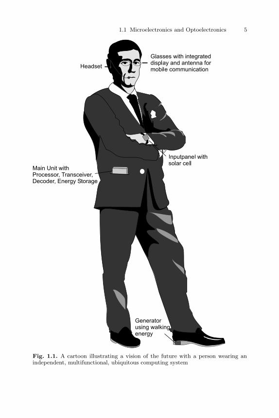
With over 300 million transistors per silicon chip on present day micro-processors, the main drive in the future is the reduction in cost per functionon a chip. Single chip or few chip solutions are significantly cheaper to man-ufacture than multiple chips for complete systems and therefore the drive istowards system-on-a-chip. Systems-on-a-chip will be realised where hetero-geneous functions as analogue, digital, high frequency, power, sensors, actu-ators and optical or microwave transmission are all combined. The personalcommunicator is a popular example where microphones, image sensors, anddisplays are combined with logic, transceivers and energy conversion/energystorage (Fig. 1.1).
Quantum effects can already be observed in existing micro- and optoelec-tronic devices. While lithographic dimensions are still much larger than thede Broglie wavelength of electrons, the vertical device dimensions, however,are up to a factor 10 smaller than lateral dimensions. Carrier abruptness atsurfaces or interfaces is only fundamentally limited by the Debye length, LD
which for electrons is given by
L2D = τRelDn =
(εrε0Vt
qND
)(1.6)
with the thermal voltage Vt = kBT/q, the donor doping level ND, the relativedielectric constant εr, the permittivity of a vacuum, ε0, the electron charge, qand the temperature, T . The relaxation time τRel and the diffusion coefficient,Dn are given by
τRel =εrε0
σn(1.7a)
σn = qµnND (1.7b)Dn = µnVt (1.7c)
with σn the specific electrical conductivity, and µn the electron mobility. TheDebye length in Si at T = 300K, is smaller than 10 nm for carrier levels above2 × 1017 cm−3.
One common example of quantum effects can be given by considering thehundreds of millions of metal contacts per integrated circuit. The currentfrom the metal contact to the semiconductor has to overcome the depletionlayer beneath the metal contact. The technological routine solution is basedon a highly doped contact formed by implantation which reduces the deple-tion width to such a small dimension that quantum mechanical tunnelling ofelectrons through the barrier dominates the current. Indeed, every transis-tor is composed of the inner transistor and three terminal tunnelling diodesconnecting the device to the interconnect metallisation. With proper tech-nology the voltage drop Vc across the tunnelling diodes is small and may beexpressed by Vc = Rc × J with current density, J and the specific contactresistance, Rc proportional to the tunnelling probability
1.1 Microelectronics and Optoelectronics 5
Fig. 1.1. A cartoon illustrating a vision of the future with a person wearing anindependent, multifunctional, ubiquitous computing system

6 1. Introduction
Rc ∼ exp
[2ΦBn
q
√εrε0m∗
h2ND
](1.8)
where ΦBn is the Schottky barrier height and m∗ the effective mass of theelectrons. If the contacts are doped in the 1020cm−3 range, specific contactresistances may be realised with values as low as 10−7 Ωcm2 to 10−8 Ωcm2.Even with extremely high current densities of 106 Acm−2, the voltage dropVc is then limited to 10mV and 100mV, respectively. Voltage limiters forvoltages smaller than 6 V are frequently based on Zener diodes, where Zenertunnelling (band to band tunnelling from the valence band to the conductionband across a high doped p/n-junction) is responsible for the voltage limitingbreakthrough. The limits of breakdown can easily be shifted between 2V and6 V by appropriate doping between 5×1018 cm−3 and 1×1018 cm−3. Heavierdoping leads to backward diodes and finally to Esaki diodes where Esakitunnelling (from conduction band to valence band) dominates in the forwarddirection (0 - 200mV) leading to negative differential resistance. Both diodetypes are not very often used in silicon microelectronics but may find a strongupsurge with heterojunctions as explained later.
The widespread use of the metal oxide silicon field-effect transistors(MOSFETs) should not be forgotten since the vast majority of low powerlogic ICs are produced using such devices. This wide spread use is related tothe basic unit of the CMOS circuit architecture, the inverter, only consum-ing significant power when switching, i.e. dynamic power. The static powerdissipation is very small as it is only related to leakage currents in the tran-sistor or circuit. The MOS inversion transistor is switched on by a gate signalcreating a thin two-dimensional surface channel with highly concentrated mi-nority carriers. The potential well for minority carriers is confined (Fig. 1.2)to the surface (inversion layer). The inversion layer thickness Zav in Si (100)is given at low temperatures by
Zav(nm) ∼= 7√ns/ (1012cm−2)
(1.9)
where ns is the sheet carrier density given by
ns =(
εoxε0
qtox
)(Vg − VT ) (1.10)
with tox the oxide thickness, εox the oxide dielectric constant, Vg the gate volt-age and VT the threshold voltage. The inversion layer thickness, Zav increasesat room temperature at most by a factor of three, because of occupation ofhigher subbands.
It was in this type of MOSFET inversion layer device and not in the laterdeveloped but higher mobility GaAs MODFET that much of the semicon-ductor physics and low dimensional devices work in the 1960s, 1970s and1980s was completed. Indeed, Klaus von Klitzing and colleagues discoveredthe quantum Hall effect using MOSFET inversion devices before the effect

1.2 From Microelectronics to Nanoelectronics 7
Ec
Ev
SiO2
gategate
Ec
Ev
SiO2
n-Si
electroninversion
layer
hole inversionlayer
EF
EF
(a) (b)
p-Si
Fig. 1.2. A schematic diagram of (a) n-MOSFET and (b) p-MOSFET showing theinversion layers for the charge carrier
was observed in GaAs devices. He was awarded the Nobel Prize in 1985 forthis achievement.
1.2 From Microelectronics to Nanoelectronics
Simply by shrinking the lateral dimensions into the sub-100nm regime andthe vertical dimensions into the sub-10nm regions (e.g. the gate dielectricsthickness will be 1.5 to 3 nm) the existing microelectronics has already beenconverted into nanoelectronics.
This definition, however, is not the usual meaning of the term nanoelec-tronics as used by many researchers; it is more frequently used to describenew types of technology such as molecules, wires and other exotic structureson the nanometre scale. For the systems use of such new technologies, con-sideration of all the properties are required including
• materials• devices• integration techniques• circuit architectures• novel applications

8 1. Introduction
Integration has been the key factor in the success story of silicon basedmicroelectronics and should be considered as an essential step when assessingthe potential of new solutions and technologies. We will therefore discuss somevisible routes in a separate section. For the other levels we will structure thediscussion by starting with the route of existing main stream technology andby comparing the new ideas with those either given by silicon based materialsor by competitive materials.
The basic transistor type of recent digital circuits is the CMOS field effecttransistor (FET) which uses inversion layers below the gate electrode (Fig.1.3) to switch on the currents. The device operation will be explained laterin the book (Chap. 5).
Fig. 1.3. The CMOS inverter scheme with a n–channel MOS (left side) and ap–channel MOS (right side). The input voltage, Vin is given to the connected gateelectrodes G, the inverted output voltage Vout is taken from the common drainelectrodes D. The source electrodes S1, S2 are on ground and at the supply voltageVDD, respectively
The large scale integration (LSI) of MOSFETs reached the million tran-sistor mark of very large scale integration (VLSI) over a decade ago and isnow at the gigascale of ultra large scale integration (ULSI)). The reader in-terested in technological details of the breathtaking advance in complexityof ICs should consult one of the books in further reading at the end of thechapter.
The CMOS transistor size is predominantly reduced to increase the pack-ing density in ICs but smaller gate length devices also benefit from higherspeed. Shrinking of the most important lateral device dimensions – the gatelength LG – seems possible down to 20 nm or perhaps even smaller beforepartially or fully depleted schemes such as silicon-on-insulator (SOI) or dou-ble gate transistor schemes are required. One major concern is the powerdissipation, as the density of transistors increases continuously by scaling. Ingeneral, the power dissipation Pdis of a CMOS circuit may be estimated fromstatic power dissipation in standby (first term, equation 1.11) and from thedynamic switching power (second term, equation 1.11)

1.2 From Microelectronics to Nanoelectronics 9
Pdis = VDDIonW10−VT /S + CLV 2DDfc
a
2(1.11)
where VDD is the supply voltage, VT is the threshold voltage, S is the sub-threshold swing (58mV for fully depleted devices to 70mV for partially de-pleted devices), W is the total width of the transistors, CL is the total nodecapacitance, fc clock frequency and a represents the transition probabilityof the logic gates. A full description of the CMOS architecture and powerdissipation is given in Sect. 10.1. The requirement for having a reasonablecurrent on/off ratio in a transistor (Ion/Ioff) in order to minimize the standbypower dictates a minimal threshold voltage
VT = logIon
IoffS (1.12)
which is more than 0.4V - 0.5V for room temperature circuits. The powersupply VDD should be at least several tenths of a volt higher than VT tocause the necessary driving current ID which is related to the gate delay by
tdelay = CLVDD
ID(1.13)
In the short–channel devices, the threshold voltage decreases as the drainvoltage Vds increases due to two–dimensional electrostatic charge sharing be-tween gate and the source/drain. Higher channel doping, retrograde verticaldoping profiles and self–aligned halo implants have been shown to signif-icantly reduce the short–channel effect around 100 nm channel length. Asthe gate oxide thickness is scaled down to below 2.5nm the gate–tunnellingcurrent increases exponentially. Alternatively, new high–k dielectric gate ma-terials may replace the thermal oxide to yield the larger capacitance of athinner oxide with an equivalent oxide thickness (EOT) while keeping thetunnelling current under control at the same time.
Multiple levels of interconnects stacked on top of the silicon chip dominatethe design and placement of transistors in present ULSI chips. Effects of theinterconnects as signal reflections, cross talk and propagation delays havebecome major barriers in the evolution of modern high–density, high–speedsystems. With the replacement of Al alloys by Cu metallization and low k–intermetal layer dielectrics (ILD) an improvement in circuit performance byat most a factor of three has been obtained. Further improvement throughnew materials is difficult as few metals have significantly higher electricalconductivity and the insulators are already close to the dielectric constantsof a vacuum. Optical global interconnects and the use of wireless microwaveinterconnects have been proposed to further improve circuit performance. Theintegration of wireless interconnects such as those in a cellular phone networkis principally possible with existing Si technology. An efficient, switchable,silicon-compatible light source such as a laser or light emitting diode (LED)still remains a major problem for the realisation of optical interconnects.

10 1. Introduction
For the ultimate CMOS scaling the short channel problems require alter-native approaches by reforming the geometrical shape and/or by introducingheterostructure barriers. The geometrical approaches are mainly based onsilicon on insulator (SOI), double gates and vertical transistors. Heterobar-riers are either used to suppress drain induced barrier lowering (DIBL) orto increase the channel performance, e.g. by strained-silicon channels whichmay be created by virtual substrates with strain relaxed SiGe on Si.
The consideration of speed in a circuit environment necessitates re–evaluation of suitable architectures for computing and signal processing. Sincethe current drive of shrunken devices with only a few electrons will be suffi-ciently small, the interconnects and fan out numbers must be small as well.The best way to alleviate the global interconnect bottleneck is to adopt dif-ferent architectures which can minimize interconnects. Neural networks (NN)and cellular automation (CA) belong to these architecture classes. The inter-ested reader is referred to the references in further reading.
Quantum mechanics offers a new fundamental unit of information, thequantum bit or qubit. In contrast to the state of a bit which is specified either”0” or ”1” the qubit can also exist in a complex superposition of both states.In addition, different qubits can be entangled within a short time providedthe respective phases are preserved. Entanglement allows massive quantumparallelism for computation entitled quantum computing. Such technology isextremely far from market and does not provide a simple general computa-tional machine (or Turing machine). Quantum computers if realised are likelyto be used for simulation of quantum systems or solving specific non-linearproblems such as factorising numbers, the travelling salesman problem ordatabase searching.
As the feature sizes of transistors are scaled down, the number of electronsdecreased and eventually reach a single electron state. In a single electrontransistor (SET) a small Si island is coupled to two external electron reser-voirs through tunnelling barriers. Because of the discrete nature of electriccharge, q, a finite charging energy q2/C (C capacity of the island) has toovercome by the next electron, a process which is called Coulomb blockade.For a 10 nm Si sphere within an oxide the charging energy, the selfcapacitanceand the ground state are given by 72meV, 2.2 aF and 3.8meV, respectively.
In our device chapters we concentrate mainly on quantum effect devicesfor room temperature operation and on single crystal heterostructure tech-nologies which are either already competitive with present technologies, canbe integrated with present technologies to produce better performance orshow the potential of near future competitiveness with present technology.
1.3 Self–ordering
The vertical nanometer structures (<20 nm) required to create substantialquantisation in Si can be easily manufactured using modern epitaxial methods

1.3 Self–ordering 11
(Chap. 2). The economic manufacturing of the lateral structures of around1011 devices per chip (roughly anticipated for 2016) is a much more criticalissue. Self-ordering of densely packed nanostructures could be an attractivealternative, especially, if new architectures with low interconnect lengths areconsidered. At present, however, the lack of an appropriate architecture com-bined with the random nature of deposition precludes the significant devel-opment of such schemes for microelectronic circuit demonstrators.
An obvious way for self-ordering uses the Stranski–Krastanov (SK) growthmode. In this growth mode, which is explained in more detail in the Chap. 2,a high number of islands (109 to 1011 cm−2) is nucleated on top of a wettinglayer (Fig. 1.4). This growth mode is favoured under certain circumstancesin strained heterostructures, e.g. in Si/Ge. Homogeneous nucleation is dom-inated by the statistics of supersaturation, leading to a rather broad distri-bution of sizes and distances. Research is devoted to heterogeneous startingconditions which may result in narrower distributions and periodical arrays.From the many approaches, we mention three ones in order to demonstratethe principles.
Fig. 1.4. Film surface and lattice plane distortion in a strained film grown in theStranski–Krastanov growth mode
In stacked multilayers the nucleation in the next layer is predominantlyabove larger islands and the distance is more regular. The nucleation on al-ready strained sites is energetically favourable, but many kinetic parameterssuch as temperature, coverage, layer spacing influence the result. Whereasthe above treatment improves the periodicity of the array it leaves the ab-solute position of the net completely undetermined. In order to position thearray, oxide windows or etched surface ridges can be used because the islandspreferentially nucleate at the window or ridge edge. Surface corrugations cre-ated by misfit dislocations act as heterogeneous nucleation centers. Periodicarrays will be created if the dislocation network is periodically arranged asobtained under certain equilibrium conditions. An arrangement of this typeis shown in Fig. 1.5.

12 1. Introduction
[110]
[11
0]
_
Fig. 1.5. An array of SiGe islands on Si with preferred nucleation on the misfitdislocation glide planes. With permission from C.Teichert, 2001
1.4 Further Reading
1. C.Y. Chang and S.M. Sze, ULSI Technology, McGraw-Hill, New York(1996)
2. S. Luryi, I. Xu, A. Zaslovsky, Future Trends in Microelectronics - TheRoad Ahead, J. Wiley, New York (1999)
3. R. Campano, Technology Roadmap for European Nanoelectronics, EC(2000)
4. K. Brunner, Rep. Prog. Phys. 65 27 (2002)5. International Technology Roadmap for Semiconductors, 2003 Edition6. C. Teichert, Physics Reports, Vol.365 Number 5-6 (2002)

2. Material Science
2.1 Growth and Preparation Methods(MBE, CVD, Implantation, Annealing)
In silicon (Si) based systems quantum effect structures need small dimensions(typically less than 20 nm), because of the high effective masses. Such dimen-sions are difficult to obtain with lateral patterning methods. Lateral struc-tures are usually first created in a surface resist layer and then transferred byetching, ion implantation, and or diffusion. Microelectronic manufacturing isexpected to reach 25 nm lateral feature sizes in the year 2010 (Tab. 2.1).
Table 2.1. Lateral structure dimensions in processor manufacturing.Source: ITRS Roadmap 2003
Year 2003 2004 2005 2006 2007 2008 2009 2010 2013 2016
Node (nm) 90 65 45 32 22
Printed (nm) 65 53 45 40 35 32 28 25 18 13
Physical (nm) 45 37 32 28 25 22 20 18 13 9
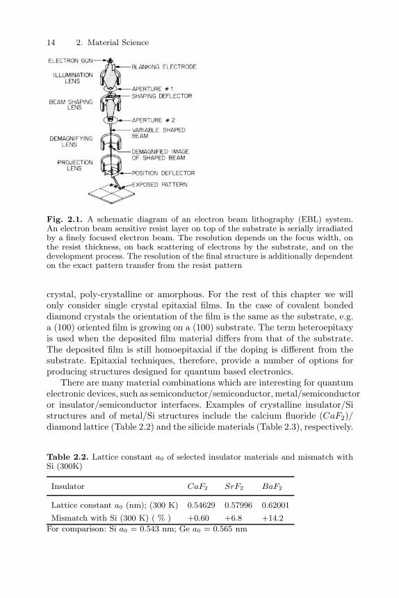
For experimental research, however, several methods with high lateralresolutions are available, predominately electron beam lithography (EBL)and focused ion beam (FIB) methods. Standard EBL (Fig. 2.1) is now usedroutinely for mask preparation for optical lithography but the writing timeincreases significantly as the resolution is increased, since EBL is a serialprocess.
The vertical control of dimensions by deposition techniques can be atleast ten times smaller than the lateral control using state of the art manu-facturing methods. The reason is the intrinsic vertical atomic layer orderingpresent in most deposition methods. A good interface normally requires asingle crystalline structure, which typically requires epitaxy conditions forthe deposition.
Epitaxy is the oriented growth on top of a substrate. The substrate isassumed to be single crystalline and the deposited epitaxial film can be single
14 2. Material Science
Fig. 2.1. A schematic diagram of an electron beam lithography (EBL) system.An electron beam sensitive resist layer on top of the substrate is serially irradiatedby a finely focused electron beam. The resolution depends on the focus width, onthe resist thickness, on back scattering of electrons by the substrate, and on thedevelopment process. The resolution of the final structure is additionally dependenton the exact pattern transfer from the resist pattern
crystal, poly-crystalline or amorphous. For the rest of this chapter we willonly consider single crystal epitaxial films. In the case of covalent bondeddiamond crystals the orientation of the film is the same as the substrate, e.g.a (100) oriented film is growing on a (100) substrate. The term heteroepitaxyis used when the deposited film material differs from that of the substrate.The deposited film is still homoepitaxial if the doping is different from thesubstrate. Epitaxial techniques, therefore, provide a number of options forproducing structures designed for quantum based electronics.
There are many material combinations which are interesting for quantumelectronic devices, such as semiconductor/semiconductor, metal/semiconductoror insulator/semiconductor interfaces. Examples of crystalline insulator/Sistructures and of metal/Si structures include the calcium fluoride (CaF2)/diamond lattice (Table 2.2) and the silicide materials (Table 2.3), respectively.
Table 2.2. Lattice constant a0 of selected insulator materials and mismatch withSi (300K)
Insulator CaF2 SrF2 BaF2
Lattice constant a0 (nm); (300 K) 0.54629 0.57996 0.62001
Mismatch with Si (300 K) ( % ) +0.60 +6.8 +14.2
For comparison: Si a0 = 0.543 nm; Ge a0 = 0.565 nm

2.1 Growth and Preparation Methods(MBE, CVD, Implantation, Annealing) 15
Different modifications, chemical instabilities, different layer stackings,thermal expansion and lattice mismatch are considerable obstacles for in-sulator application in single crystalline devices, whereas silicides are widelyaccepted as contact materials. Chemical similarity and good lattice matchare the essential factors for the ability to grow high quality covalent semicon-ductor/semiconductor interfaces.
Table 2.3. Lattice mismatch of selected metal / Si interfaces
Silicide MnSi2 FeSi2 CoSi2 NiSi2 T iSi2 PtSi
Lattice type tetra- tetra- cubic cubic ortho- ortho-
gonal gonal rhombic rhombic
Lattice mismatch ( % ) 1.7 0.9 1.2 0.4 - 9.5
Within the group IV column of the periodic table (Table 2.4) silicon andgermanium have a completely miscible alloy (Si1−xGex) with lattice mis-matches ranging from 0 to 4.2% for pure Ge lattice matched to silicon. Car-bon concentrations between 1018 cm3 and 1021 cm3 may be incorporated intoSi or Ge lattice sites under metastable growth conditions.
Table 2.4. Properties of Group IV compounds (diamond or zincblende lattice)
Compound C α − SiC Si Ge α − Sn
(diamond) (3C)
Lattice constant 0.3567 0.436 0.5431 0.5646 0.65
a0 (nm)
Indirect Bandgap 5.45 2.2 1.12 0.66 0
(Eg,ind in eV)
Direct Bandgap 6.5 3.2 0.80 0
(Eg,dir in eV)
Miscibility with Si < 3 % , < 20% - complete only
metastable metastable
Under equilibrium, the carbon (C) concentration is low (1017 cm−3 attemperatures below the melting point) with the carbon being mainly incor-porated at interstitial sites. Some additional material properties of the SiGesystem are given in Table 2.5. The completely miscible Si1−xGex alloy fol-lows rather closely a linear dependence (Vegard’s law) (mismatch f to Si: f

16 2. Material Science
Table 2.5. Properties of Si and Ge
Material Si Ge
Bandgap (eV) 1.12 0.66
Electron affinity χ (V) 4.05 4.0
Effective masses
of heavy holes mhh/m0 0.49 0.28
Effective masses
of light holes mlh/m0 0.16 0.044
Effective masses of (100) electrons
in longitudinal direction ml/m0 0.98 1.64
Effective masses of (100) electrons
in transversal direction mt/m0 0.19 0.082
m0 = 9.1091 × 10⁻³¹kgNote: The conduction band minimum for Ge is in the (111) direction (L-point) butfor nearly all strained SiGe alloys the minimum occurs in (100) direction (X-Point).For interpolation the properties of L-electrons in Ge ( ml = 1.64, mt = 0.082)should not be used.
= 0.042x) with a small quadratic deviation (Fig. 2.2). The lattice constantaSiGe is given exactly by
aSiGe = 0.5431(nm) + 0.01992x(nm) + 0.0002733x2(nm) (2.1)
Fig. 2.2. The lattice constant, aSiGe, of the SiGe alloy as a function of the Gecontent x. The solid line compares Vegard’s law with experimental values (crosses)
In Si based microelectronics the most important surface orientation isthe (100) orientation at which the best controlled amorphous oxide/silicon
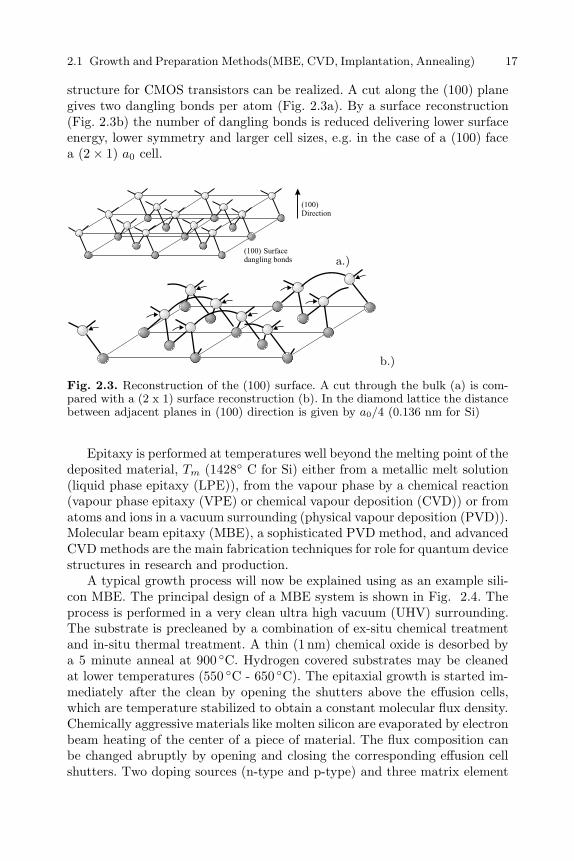
2.1 Growth and Preparation Methods(MBE, CVD, Implantation, Annealing) 17
structure for CMOS transistors can be realized. A cut along the (100) planegives two dangling bonds per atom (Fig. 2.3a). By a surface reconstruction(Fig. 2.3b) the number of dangling bonds is reduced delivering lower surfaceenergy, lower symmetry and larger cell sizes, e.g. in the case of a (100) facea (2 × 1) a0 cell.
a.)
b.)
Fig. 2.3. Reconstruction of the (100) surface. A cut through the bulk (a) is com-pared with a (2 x 1) surface reconstruction (b). In the diamond lattice the distancebetween adjacent planes in (100) direction is given by a0/4 (0.136 nm for Si)
Epitaxy is performed at temperatures well beyond the melting point of thedeposited material, Tm (1428 C for Si) either from a metallic melt solution(liquid phase epitaxy (LPE)), from the vapour phase by a chemical reaction(vapour phase epitaxy (VPE) or chemical vapour deposition (CVD)) or fromatoms and ions in a vacuum surrounding (physical vapour deposition (PVD)).Molecular beam epitaxy (MBE), a sophisticated PVD method, and advancedCVD methods are the main fabrication techniques for role for quantum devicestructures in research and production.
A typical growth process will now be explained using as an example sili-con MBE. The principal design of a MBE system is shown in Fig. 2.4. Theprocess is performed in a very clean ultra high vacuum (UHV) surrounding.The substrate is precleaned by a combination of ex-situ chemical treatmentand in-situ thermal treatment. A thin (1 nm) chemical oxide is desorbed bya 5 minute anneal at 900 C. Hydrogen covered substrates may be cleanedat lower temperatures (550 C - 650 C). The epitaxial growth is started im-mediately after the clean by opening the shutters above the effusion cells,which are temperature stabilized to obtain a constant molecular flux density.Chemically aggressive materials like molten silicon are evaporated by electronbeam heating of the center of a piece of material. The flux composition canbe changed abruptly by opening and closing the corresponding effusion cellshutters. Two doping sources (n-type and p-type) and three matrix element

18 2. Material Science
Fig. 2.4. A schematic diagram of the silicon MBE process. The substrate ismounted on top and heated from the backside by an infrared heater. The molecularbeams are evaporated from separate thermal sources (effusion cells for the dopantsand germanium or carbon, electron beam evaporators for silicon and sometimesalso for germanium). In situ monitoring is achieved by several methods, here aquadrupole mass spectrometer (QMS) for flux measurements is shown
sources (Si, Ge and C) are the minimum source configuration with additionalpossibilities for other sources (metals, insulators, gases).
The growth process is monitored by in-situ analysis with electrons and op-tical beams. Examples are reflection high energy electron diffraction (RHEED)to observe the surface; electron induced emission spectroscopy (EIES) orquadrupole mass spectrometry (QMS) for individual flux control; pyrometryor thermoelectric voltage measurement of temperatures; and ellipsometry orreflection interferometry for film thickness monitoring. A clean surface turnedout to be an essential prerequisite for reducing the growth temperature fromthe usual 1050 C-1150 C to 500 C-700 C. Even lower temperatures are re-quired if the limits set by amorphous growth at 100 C to 200 C are to bereached. The substrate is radiation heated by a graphite meander mountedon the backside of the substrate. Several kilowatts of power are needed tooperate the sources and the substrate heater. During operation the pressureraises from the base pressure of 3×10⁻¹¹ mbar to the 10−10 mbar range. Thisis acceptable as long as hydrogen (H2) is the dominating gas which has to bemonitored by residual gas analysis (Note: The unit mbar is 100 times the in-ternational unit Pascal (Pa) = 1Nm−2, atmospheric pressure (AP) is roughly105 Pa). The pressure defines the molecular density which is about 1013 m−3
in the given pressure regime producing a mean free path for a molecule ofabout 100 km. This defines the impinging rate on a wall (1015 m−2) and the

2.1 Growth and Preparation Methods(MBE, CVD, Implantation, Annealing) 19
time for monolayer coverage of a surface (104 s/S, when S is the sticking co-efficient of a specific gas). A technical system (Fig. 2.5) needs in addition tothe growth chamber additional UHV-chambers for a load lock, wafer stor-age, pretreatment and analysis. A wafer transfer system transports the waferbetween the load lock and the wafer storage or the wafer holder.
Fig. 2.5. A commercial (Leonardo) three chamber Si-MBE system with the mainchamber for growth, a storage chamber with a 25 wafer magazine, and a loadlock. UHV-conditions are maintained by two turbomolecular pumps, a titaniumsublimation pump and an ion getter pump. The transfer system operates from thestorage chamber
Standard silicon CVD (Fig. 2.6) is typically carried out at atmosphericpressure and involves the pyrolysis at an elevated temperature of the pre-cursor gas of silane or silicon halide (SiH4−zClz with 1 ≤ z ≤ 4). Radiofrequency coils are used to heat the system to temperatures ranging from900 oC to greater than 1100 oC to volatilise nominally contaminating speciessuch as water, oxygen or carbon.
While such high temperature can be tolerated for the homoepitaxial blan-ket growth of silicon onto a silicon wafer without dopants, the addition of ei-ther doping or germanium into the growth system requires significantly lowertemperatures. Autodoping occurs at temperatures above 1000 oC which in-volves the diffusion of dopants from the substrate into the epitaxial film cre-ating unwanted anisotropic distortions in the epitaxial layer. The reductionof the system operating pressure serves to eliminate a slowly floating bound-ary layer of gas immediately above the substrate, allowing the more rapid

20 2. Material Science
transport of evaporated dopant away from the substrate, thus reducing theauto-doping effect. The reduction of the operating temperature also reducesboth the rate of dopant evaporation into the gas stream and solid state dif-fusion. For strained Si1−xGex layers there are two main problems with hightemperature. The first is the roughing or development of surface undulationsfrom high temperature growth and the second is diffusion of the germanium.The activation energy and diffusivity of Ge from a Si0.7Ge0.3 layer into sili-con have been measured to be 4.7 eV and 0.04 m2/s respectively suggestingdiffusion of some nanometers even at a temperature of 1000 oC for 1 minute.
As the growth temperature for CVD is reduced, lower background pres-sures are required to maintain an oxide free silicon surface to grow on. Oxygencontent in Si1−xGex films has been demonstrated to substantially reduce theminority carrier lifetime in the films, an important property for bipolar tran-sistors. Chemical equilibrium data for the maintenance of an oxide free siliconsurfaces demonstrates that it is the partial pressure of water which is the lim-iting effect and requires ultra high vacuum background chamber pressures forlow temperature growth.
A number of different CVD reactors have been developed for the lowtemperature growth of strained Si1−xGex films. These can be convenientlydivided into ultra-high vacuum CVD (UHV-CVD) at growth pressures of lessthan 10 Pa and low pressure CVD (LPCVD) with pressures ranging from 10to 1000 Pa. Other systems do exist but most have been research tools andhave not been developed into production tools. Source gases for CVD includeSiH4, Si2H6, SiH2Cl2 and GeH4 while doping is achieved using AsH3, PH3
and B2H6. The majority of commercial LPCVD reactors are single wafertools while the IBM UHV-CVD system is a batch tool allowing growth of 25wafers or more at a time.
Whatever is the method of deposition of the epitaxial layer, the result isan atom sticking to the surface. These adsorbed atoms are called adatomsand are a precursor state before the atoms are incorporation into the lattice.The adsorption energy, Ead is lower than the binding energy, E of an atomin the crystal, usually 1
2E to 23E. When an atom is moving toward the sur-
face (Fig. 2.7) the balance of attractive and short ranged (atomic radius)repulsive atomic forces create a potential well at the equilibrium position forthe adatom. In order to stick at this adatom position, the atom or moleculemust transfer its energy, momentum and moment of torque to the solid. Ifthis does not happens rapidly enough, as is often the case with moleculeswith a moment of torque, we refer to a sticking coefficient S smaller thanunity.
Even if the adatom is adsorbed, the adatom may later escape by a desorp-tion step caused by thermal vibrations. If there is an equilibrium between thesolid and the vapour phases, the adsorption and desorption events are bal-anced. For growth the vapour pressure has to be higher than the equilibrium

2.1 Growth and Preparation Methods(MBE, CVD, Implantation, Annealing) 21
Fig. 2.6. A schematic diagram of a CVD epitaxy tool
Fig. 2.7. The potential energy as function of distance to the surface for the ad-sorption of adatoms
pressure (supersaturation). The flux F impinging on a surface is connectedto the vapour pressure, p by
F = p
√NA
2πMkBT(2.2)
where NA = 6.022× 1029 m−3 is Avogadro’s number and M is the molecularweight.

22 2. Material Science
In a simple picture the desorbing flux Fdes is proportional to the adatomdensity ns and the Boltzmann probability of an energetic thermal vibration.
Fdes = nsωq exp− Ead
kBT
(2.3)
where ωq is the frequency of thermal vibrations usually assumed as 1012 Hzto 1013 Hz (see Sect. 3.6).
A regular network of surface positions is available for the adatoms. Indeed,we have to assume that adatoms can easily jump from one position to another,a process which is described as surface diffusion with an activation barrierUS . The diffusing atom may desorb or may be incorporated into the crystal.The energy gain for the incorporation from an adatom place is Es whereEs + Ead = E (Fig. 2.8). In a 70 years old ”Gedankenexperiment” Kosselshowed that repeated joining of atoms to kinks on surface steps deliverscontinuous crystal growth with every atom gaining the binding energy whenincorporated at the kink.
Fig. 2.8. A schematic diagram of the incorporation of adatoms. The process in-volves the adsorption of the adatom (with energy gain Ead), the surface diffusion(with energy barrier US) and the incorporation of the adatom in the crystal at asurface step (with binding energy E)
The equilibrium concentration of adatoms nS0 is then given by the balancebetween the adatom position and any energetically favourable step positions.
nS0 = NS exp− ES
kBT
(2.4)
where NS is the surface density of atoms. The diffusion coefficient DS is givenby

2.1 Growth and Preparation Methods(MBE, CVD, Implantation, Annealing) 23
DS =1
NSν exp
− US
kBT
(2.5)
where the mean distance between neighbouring adatom places is given by√1
NS. Before an adatom can be adsorbed it walks on average for the desorp-
tion time, τDes which defines a diffusion length λS on the surface of
λS =√
DS τDes =√
1NS
exp
Ead − US
2kBT
(2.6)
Note that under growth conditions, the incorporation of the adatom inthe crystal is a competing process to the desorption process and thereforethe majority of adatoms will walk smaller distances than given by λS .
Let us now consider a growth experiment by supplying fluxes F of thedifferent matrix and doping elements to a surface. For one element we definea linear supersaturation σ by
σ =F
F0− 1 (2.7)
(F0 equilibrium flux of the element given by F0 = nS0/τDes).On the surface the adatom concentration nS will also increase above the
equilibrium value nS0. We define a surface supersaturation σS by
σS =nS
nS0− 1 (2.8)
Depending on the composition, three different basic growth modes arepossible (Fig. 2.9).
Fig. 2.9. The basic growth modes of two-dimensional (or Frank–v. d. Merwe)growth (2D), three-dimensional (or Volmer–Weber) growth (3D) and a mixturefrom 2D to 3D growth, the Stranski–Krastanov mode
A qualitative understanding is possible by using the droplet model (Fig. 2.10)where the force balance at the rim of a droplet is considered. The surfacetension Σ (specific surface energy) is composition dependent, the interfaceenergy Σi depends also on the strain and dislocation structure.

24 2. Material Science
ΣS = Σi + Σf × cos(Θ)3D growth : ΣS − Σi < Σf
2D growth : ΣS − Σi > Σf
Fig. 2.10. The droplet model of three-dimensional island growth. The force be-tween the surface tensions of ΣS and Σf balanced by the interface energy Σi leadsto an island inclination angle Θ when ΣS − Σi < Σf
The most simple case is homoepitaxy, the growth of for example a Siepilayer on a Si substrate. The minimum surface energy is obtained by two-dimensional, flat growth. The surface morphology involves atomic steps ofusually monolayer (h) or bilayer (2h) thickness. The low temperature regime(below 100C for Si), where amorphous or highly defective growth proceeds,or the high temperature regime (above 1250C for Si), where surface roughen-ing occurs, are not taken into account, because these regimes are not presentlyused for the growth of epilayers which are used in quantum electronic struc-tures. On silicon where the dislocation density is negligible, there are twosources which create surface steps. At higher temperatures (roughly aboveTm/2, Tm melting point, Si ≈ 1700 K) steps from the misorientation, i,of the substrate are present. Even with nominally oriented substrates (e.g.(100)) a small misorientation (i < 0.5, arc i ∼= tan i < 0.0085) is techni-cally unavoidable which leads to terraces of width > 15 nm separated bymonoatomic steps. At lower temperatures (roughly below Tm/2) adatomsare not fast enough to move to the steps and nucleate into two-dimensionalislands (Fig. 2.11). When all adatoms reach the already existing misorienta-tion steps (in substrates which are not as perfect as Si the dislocation stepsalso act in a similar way) the monoatomic steps move laterally forward bythe adatom capture (step flow).
When at the lower temperatures in which two-dimensional nucleationtakes place, the adatoms can join to the steps at the rim of the nucleus withinsmaller distances. The nuclei grow and coalesce to form a single monolayer,so that the 2D nucleation is a periodic process. A critical nucleus (Fig. 2.12)is defined by the size in which the growth by the capture of adatoms is moreprobable than the decay of the nucleus.
Therefore with high supersaturation which results in high adatom densitythe critical size of the nucleus is smaller. For the extremely high supersatu-ration which occurs during Si-MBE, two joining adatoms probably alreadycreate a critical nucleus. The basic picture is somewhat blurred by the loss ofsymmetry from the surface reconstruction which results in highly anisotropicdiffusion and two step types with different kink densities (Fig. 2.13). A de-tailed discussion is beyond the scope of this book. In either case the minimum

2.1 Growth and Preparation Methods(MBE, CVD, Implantation, Annealing) 25
Fig. 2.11. The two-dimensional growth by step flow or 2D island nucleation (sideview)
Fig. 2.12. The two-dimensional nucleation (top view). The size of the nucleusfluctuations and a critical nucleus size is achieved when several adatoms have joined.The size and binding energy of this nucleus is high enough that a decay of thenucleus is less probable than the further growth by adatom capture
step density is defined by the misorientation. In the step flow regime the num-ber of steps is constant whereas in the 2D nucleation regime the step densityoscillates above the minimum step density. With very sensitive surface mon-itoring methods like electron diffraction (RHEED) these oscillations in the2D nucleation regime can be observed through intensity variations.
We will treat as an example the simplest case of step flow within the frame-work of a theory developed by Burton, Cabrera, and Frank (BCF-theory).Let us consider a regular array of misorientation steps (Fig. 2.14). The terracewidth L is defined by the misorientation i.
h
L= tan i ≈ arg i (2.9)

26 2. Material Science
Fig. 2.13. A scanning tunnelling microscopy (STM) image of a Si (100) surfacedepicting two different step types (SA, SB) along with separation terraces with(2 × 1) and (1 × 2) reconstructions
Fig. 2.14. A regular array of misorientation steps. The misorientation (inclinationi) leads to terraces of width L separated by steps with height h. The steps moveby the capture of adatoms on sites with kinks
The BCF-theory is a surface diffusion theory with specific conditions forparticle conservation at the steps. Generally particle conservation is describedby the continuity equation,
dnS
dt+ ∇ · S = GS − RS (2.10)
S = −∇nS (2.11)
where S is the surface flux vector, GS , RS the generation and recombinationrates, respectively. The trick in the BCF-theory is the choice of the bound-ary conditions of (2.10). Only the terraces are considered where the stepsare outside. With this choice and the assumption that the adatoms are onlycaptured at steps, the recombination term in the differential equation con-tains only the desorption term. The adatom incorporation, therefore, will betreated by the boundary conditions.

2.1 Growth and Preparation Methods(MBE, CVD, Implantation, Annealing) 27
In the one-dimensional (coordinate y- perpendicular to the steps alongthe surface) and stationary form (dnS
dt = 0), the equation reads
d2nS
dy2λ2
S − nS + FτDes = 0 (2.12)
If we use the assumption that the step acts as a perfect sink (Fig. 2.15) foradatoms, the boundary conditions may be written as nS = nS0, at y = ±L
2(the y-axis origin is given between two steps to obtain symmetrical solutions).The solution for the local surface supersaturation is given by
σS =nS
nS0− 1 = σ
[1 − cosh y
λS
cosh L2λS
](2.13)
with σ = FF0
− 1, cosh(u) = 12 [exp(u) + exp(−u)].
The adatom concentration has its maximum half way between two steps.The local concentration gradient drives a diffusion flux |S| which is highestat the steps.
Fig. 2.15. Local concentration of adatoms on a step array. BCF-theory with theassumption of steps as perfect sinks for adatoms.
The simple BCF-theory of step flow describes the homoepitaxial growthof MBE-silicon fairly well in the temperature regime between roughly 550 Cand 900 C. The lower temperature bound is caused by the onset of two-dimensional nucleation which is well documented by the appearance ofRHEED oscillations. The transition temperature depends on the misorien-tation i (with terrace length L) and growth rate R (for supersaturation σ).The upper temperature bound is caused by surface defects and the surfaceroughening which allows adatoms to also be incorporated outside the stepsand nuclei. This temperature value is uncertain, because MBE experimentsare usually well below 900 C and in CVD experiments the surface kineticsare overlapped by mass transport in the vapour phase, by chemical reactionsand by adsorption of hydrogen and reaction products.

28 2. Material Science
In the typical Si-MBE temperature regime of step flow growth (typically550 C-750C) a further simplification of the BCF theory can be made. Si-desorption is very weak in this temperature regime and can be neglected,which is mathematically described by the inequality λS L. The differentialequation (2.12) then reads
DSd2nS
dy2+ F = 0 (2.14)
with the solution for the step array
nS − nS0 =F
2DS
[(L
2
)2
− y2
]. (2.15)
We will now give a simple example, where we choose a temperature T =900K (627C), F = 7 × 1014cm−2s−1 (1 monolayer (ML) per second), L =30 nm (i = 1
4
), ES = 2.0 eV, US = 0.6 eV, ωq = 1013 Hz. Then we calcu-late a low value for the equilibrium adatom density nS0 = 1.84×103 cm−2,a rather high surface diffusion coefficient DS = 4.8×10⁻⁶ cm−2Hz describ-ing the good surface mobility of adatoms and a maximum adatom densityof nSmax between two steps (y = 0) of nSmax = 1.5×108 cm−2. The equi-librium adatom density is already low and decreases steeply with decreasingtemperature (70 K decrease yields an order of magnitude decrease in nS0).The diffusion coefficient also decreases but more slowly with the temper-ature (a 200K temperature decrease is needed for an order of magnitudedecrease in DS corresponding to the lower activation energy). The maximumadatom density increases with decreasing temperature as ( 1
DS). This increase
in adatom density favours two-dimensional nucleation at lower growth tem-peratures. To prove the inequality λS L we calculate τDes = 60 s (Ead =2.55 eV is assumed) and λS = 17µm which is 500 times higher than the stepdistance L. The diffusion length increases with decreasing temperature withan activation energy of 1
2 (Ead − US).The simple assumption that a step acts as a perfect sink for adatoms
can be replaced by more sophisticated models. In one of these models theadatoms at the upper terrace have to overcome an energy barrier (Schwoebelbarrier) to be captured. This model predicts step bunching where a steparray is separated in regions with lower step densities and ripples with higherstep densities. In Si, step bunching is probably also influenced by diffusionanisotropy and step energies.
The BCF-theory is not applicable to segregating dopants, because thesteps then lose their sink properties, or to strained heteroepitaxial layers,because then the diffusion of adatoms is not solely controlled by the concen-tration gradients but also by chemical and strain gradients.
In an epitaxial growth process the technologically controlled parametersare the substrate orientation, the material flux and the growth tempera-ture. From the BCF theory we learned that the adatoms behave like a two-

2.2 Segregation and Diffusion of Dopants and Alloy Materials 29
dimensional atom gas with much higher diffusivity in the plane of the surfacethan in the bulk. The laws of surface physics govern the movement of anatom to its final position in the crystal.
At the moderate temperatures used for the epitaxial growth of quantumdevice structures, each atom is effectively fixed in its position in the bulk. Thebulk diffusivity is determined by the diffusion of lattice defects (vacancies,interstitials) and the positional interchange between an atom and a defect.The equilibrium concentration and the mobility of these defects decreaseswith temperature, so the bulk diffusivity, D of substitutional dopants reduceswith temperature rather steeply (typical activation energies EA around 4 eV).
D = D0 exp(−EA
kBT
). (2.16)
For example with D0 = 0.1m2s−1, EA = 4 eV, T = 900K, time t =3600 s one obtains a bulk diffusion coefficient D = 4 × 10⁻²⁶ m2s−1 whichis 16 orders of magnitude lower than the calculated surface diffusivity. Thediffusion length 2(Dt)
12 amounts to 2.4 × 10⁻¹¹ m.
The processing of many quantum device structures may need high thermalbudget processing including the annealling of any implants, thermal oxidationand silicide formation. Most of these processing steps require temperaturesabove 800 C where bulk diffusion cannot be neglected. The equilibrium dif-fusion may be masked at this temperature regime by what is known as tran-sient enhanced diffusion (TED). Transient enhanced diffusion is caused bya nonequlibrium concentration of point defects (vacancies, interstitials) withwhich an atom can exchange its position. Implantation, oxidation, nitrideformation and silicide formation, especially at lower temperatures, severelydisturb the point defect equilibrium. A very precise method to measure TEDis given by observing the out diffusion of δ-doped layers after point defectinjection.
2.2 Segregation and Diffusion of Dopants and AlloyMaterials
The replacement of a Si atom in the crystal lattice by a dopant atom (sub-stitutional impurity) delivers the extrinsic semiconductor properties requiredfor device operation. Group III materials and Group V materials as dopantsresult in hole conduction (p-type) and electron conduction (n-type) for GroupIV semiconductors, respectively. The most important p-type dopant in sili-con is boron (B), important n-type dopants are phosphorus (P), arsenic (As)and antimony (Sb). A selection of Group III to Group V elements is shownin Table 2.6.
Important parameters for dopant atoms are the covalent radius (the radiusin a covalent bond which is roughly the atomic radius without the outer

30 2. Material Science
Table 2.6. Part of the Periodic Table of elements showing a selection of dopantand alloy elements for silicon. Lower indices show the atomic mass number andupper indices the atomic number of each element
Main Group
III IV V
B510.8 C6
12.0 N714.0
Al1327.0 Si1428.1 P 1531.0
Ga3169.7 Ge32
72.6 As3374.9
In49114.8 Sn50
118.7 Sb51121.7
shell electrons), the chemical behaviour, the solid solubility and the diffusionconstant. The atomic radius of nitrogen is too small for a substitutionalposition in Si, it therefore fails as a donor in Si. Boron and phosphorus aresmaller than Si (covalent radius of Si: 0.117 nm), therefore thick and heavilydoped layers are under tensile strain. Arsenic has a near identical covalentradius to Si, therefore heavily n-doped layers (e.g. buried layers for collectorcontacts) are preferably As doped. Antimony (as Ga, In) is larger than Si,which results in compressively strained layers. The maximum solid solubilityis obtained 100 C to 150 C below the melting point. It ranges from about1021 cm−3 for B and As to several 1018 cm−3 for Ga. At the low temperaturesused for the fabrication of many quantum effect devices the solid solubilitiesare considerably lower, but metastable high solubilities can be obtained easily.From the four main dopants B, P, As, Sb the former two (B, P) diffusefaster than the later ones (As, Sb). At lower process temperatures (< 850 C)transient enhanced diffusion (TED) created by nonequilibrium point defectconcentrations has to be considered.
During growth at lower temperatures the phenomenon of surface segrega-tion turned out to be the most important transport mechanism of dopants.To explain this phenomenon, consider a two atom system with matrix atoms(e.g. Si) and dopant atoms (e.g. Sb). The impinging matrix atoms are in-corporated at steps (either from misorientation or from nucleation) and thesteps move forward due to this mechanism. Surface segregation occurs whenthe second atom (dopant) is not incorporated into the first but manages tocontinue to reside on the growing surface. This can happen by either climb-ing across the steps or by an atomic exchange (Fig. 2.16) from a subsurfaceposition to a surface (adatom) position. The driving force for this exchangestems from an energy gain when comparing the pair dopant atom/matrixadatom (initial state) with matrix atom/dopant adatom (final state).
It is immediately clear, that a BCF-type of diffusion theory with itsadatom capture at steps cannot describe a segregating dopant. In the case ofa strongly segregating species we can completely neglect the matrix steps andassume a locally homogeneous adatom density of dopants, nS (note: in BCF

2.2 Segregation and Diffusion of Dopants and Alloy Materials 31
Fig. 2.16. The surface segregation of a dopant atom (grey) on a growing matrixsurface. For simplicity, step flow growth of the matrix is assumed and an atomicposition exchange is shown
theory the term nS was used for the matrix adatom density). The continuityequation (∇S = 0)
dnS
dt= F − nS
τDes− ND × R (2.17)
where ∇ · S = 0, because of the locally homogeneous concentration, nS, theparticle gain is defined by the dopant flux F , the particle loss is described bydesorption with a mean desorption time τDes and by partial incorporationinto the bulk (ND is the bulk donor concentration of the dopant (NA is theequivalent bulk acceptor concentration), R growth rate). Equation 2.17 con-tains three technology dependent quantities F (dopant flux), R (growth ratedependent on matrix flux) and τDes (desorption time dependent on growthtemperature). There are also the two variables nS and ND. In a first approx-imation (valid at least at low concentrations) a direct relation between nS
and ND is assumed.
∆S =nS
ND(2.18)
The segregation width ∆S is a measure of the relationship betweenadatom density nS and incorporated bulk density ND (Note: Sometimes theadatom density nS is compared with the bulk dopant atoms in a monolayerND × h which gives a dimensionless segregation ratio). Then the differentialequation reads
dnS
dt+ nS
(1
τDes+
1τinc
)= F (2.19)

32 2. Material Science
with τinc = ∆S
R incorporation time
or in the equivalent form for ND as function of growth thickness Z = Rt
dND
dt+ ND
1R
(1
τDes+
1τinc
)=
F
R∆S(2.20)
The characteristic time constant for obtaining equilibrium is given by(1
τDes+ 1
τinc
)−1
. In the case of negligible desorption (τDes → ∞) this timeconstant is completely described by segregation with τinc. To give an example,let the flux F switch on and off after a time t0 (Fig. 2.17), then the adatomconcentration, nS and the bulk doping profile follow with an exponentialdecay.
Switch on (τDes → ∞):
nS = F × τinc
[1 − exp
(− t
τinc
)](2.21a)
ND =F
R
[1 − exp
(− Z
∆S
)](2.21b)
Switch off:
nS = F × τinc
[1 − exp
(− t0
τinc
)]exp
(− t − t0
τinc
)(2.22a)
ND =F
R
[1 − exp
(− Z0
∆S
)]exp
(−Z − Z0
∆S
)(2.22b)
So, segregation converts an abrupt flux profile into a smeared doping pro-file. At low epitaxy temperatures, this mechanism has to be considered forall nanometer structures. The segregation is especially strong for Sb in Siand may be studied easily with these elements. The fundamental behaviour(Fig. 2.18) is that above a transition temperature T ∗ (which is 550 C-600 Cfor Sb/Si), the segregation width follows an equilibrium law with an acti-vation energy which is given by the gain of a position exchange. Below thetransition temperature, segregation is kinetically limited as one can easilyunderstand when you consider that in a typical growth experiment roughlyevery second a monolayer is grown. When the adatom cannot manage toclimb onto the next layer within one second it is buried and practically fixed,because bulk diffusion is much slower than surface processes.
Several strategies have been developed to overcome the limitations set bysegregation. A number of these strategies are listed in Table 2.7.Common strategies include the growth and co-evaporation at low tempera-tures where the segregation width is limited by kinetic effects along with thepre-build up and flash off of an adatom concentration before and after growthof the doped layer. Other techniques are the solid phase recrystallization of adeposited amorphous layer, implantation of dopants (Fig. 2.19) and the useof surfactants. Surfactants are accessorily added surface atoms which modify

2.2 Segregation and Diffusion of Dopants and Alloy Materials 33
Fig. 2.17. The smearing of the profile by surface segregation. A rectangular fluxprofile is assumed between t = 0 and t = t0 (a.). The adatom density nS(t) (b.)and the bulk profile ND(Z) (c.) demonstrate an exponential decay depending onthe value of the segregation width ∆S and the corresponding incorporation timeτinc = ∆S/R
Table 2.7. Doping strategies to overcome segregation. Typical temperatures aregiven for the Si/Sb system
strategy typical temperatures (Sb/Si)
coevaporation 325 C - 450 C
pre-build up / flash off 450 C - 800 C
solid phase epitaxy (SPE) 100 C - 550 C
doping by secondary implantation (DSI) 550 C - 600 C
direct implantation 500 C - 700 C
surfactant 450 C - 600 C

34 2. Material Science
Fig. 2.18. The segregation width of Sb in Si. Kinetic limitations reduce the segrega-tion width strongly below a transition temperature T ∗. The transition temperatureT ∗ depends on the growth rate R
the surface energy, in our example a third kind of atom: matrix, dopant, sur-factant. Examples of successful surfactants are heavily segregating elementswhich suppress the segregation of the intended dopant or alloy. Examples ofsurfactants in Si are As, Sb, Bi, Ga, Sn and atomic Hydrogen (H).
Fig. 2.19. Doping by secondary ion implantation (DSI). A segregation dopantadatom (grey) is pushed into the lattice by an accelerated matrix ion (typical ionenergies are several hundred electron volts)

2.3 Lattice Mismatch and its Implicationon Critical Thickness and Interface Structure 35
2.3 Lattice Mismatch and its Implicationon Critical Thickness and Interface Structure
In general, a lattice mismatch will be between a film material (such as an epi-taxial layer) and a substrate. We consider the thick substrate as the referencecrystal and define the lattice mismatch f for cubic crystals as:
f =af − a0
a0(2.23)
where af and a0 are the lattice constants of the film and the substrate,respectively.
Nature has several answers for the growth of single crystalline mismatchedfilms:
• Film accomodation by strain (elastic accomodation; pseudomorphic growth)• Film accomodation by misfit dislocations at the interface (plastic relax-
ation)• Morphological relaxation by surface undulations• Cracks
As a starting point, let us consider a strained film on a rigid substrate(Fig. 2.20).
Fig. 2.20. Elastic accomodation of a film cell to the substrate mesh
A larger film cell fits to the substrate cell by being compressed in theplane of the interface, and becomes a smaller film through tension. In thevertical direction, the opposite strain results following the laws of elasticity.A cubic cell will be transformed into a tetragonal one by the biaxial stress inthe interface (Fig. 2.21) (stress σx = σy = σ, σz = 0).
The strain components, εx,y,z follow from isotropic elasticity theory
εx = εy = ε =1 − ν
Eσ (2.24a)
εz = −2ν
Eσ = − 2ν
1 − νε (2.24b)
36 2. Material Science
Fig. 2.21. Biaxial stress leading to a tetragonal deformation
with E the elastic modulus and ν Poisson’s number. Both elastic modulesare connected with the shear modulus µ by
µ =E
2(1 + ν)(2.25)
For example, elastic relaxation of a film with lattice mismatch f and strainε cancel each other if there is elastic accommodation of the strain in the film.
ε + f = 0 elastic accommodation (2.26)
The energy Ehom of a homogeneously strained layer is proportional to thesquare of the strain and linearly dependent on film thickness t.
Ehom = 2µ1 + ν
1 − νε2t (2.27)
A finite substrate is bent by the stress. If equal elastic constants for thefilm and the substrate are assumed, the curvature (1/ρ with ρ radius ofcurvature) is a measure of the strain ε.
1ρ
= 6εt
tS
2
ts substrate thickness (2.28)
With increasing thickness (and increasing elastic energy) other accommo-dation mechanisms start to be favourable. Let us first consider accomodationof strain by misfit dislocations at the interface (Fig. 2.22). When the filmcell is larger than the substrate cell, some atomic planes will end at the in-terface without continuation into the film. This kind of atomic line defectis called a dislocation. The essential properties of a dislocation are shownin (Fig. 2.23). The dislocation line has a direction l, the deformation fieldaround the dislocation is characterized by the Burgers vector b.
The Burgers vector is easily found by surrounding the dislocation in aclosed cycle (1, 2, 3, ..., 8 in Fig. 2.23) and then projecting the path intoan ideal crystal (1’, 2’, 3’...8’ in Fig. 2.23). In the ideal crystal the path canbe closed only with an additional vector b, the Burgers vector. The Burgersvector of a single dislocation is conserved whereas the direction may change.The plane defined by the line direction and the Burgers vector (b × l) is

2.3 Lattice Mismatch and its Implicationon Critical Thickness and Interface Structure 37
Fig. 2.22. Lattice mismatched films. Left side: a pseudomorphic film by elasticaccommodation. Right side: a strain relaxed layer with a misfit dislocation in thecentre
Fig. 2.23. Elements of a dislocation. Line direction l, Burgers vector b, glide plane
called the glide plane. Dislocations can easily move within this plane becauseonly small atomic displacements are necessary for gliding. Movements outsidethe glide plane (called climbing) require generation or annihilation of pointdefects (vacancies, interstitials).
The energy Eds of a single dislocation is given by,
Eds = A
[ln
ra
ri
]with A =
µb2
4π(1 − ν)(2.29)
where µ is the shear modulus, b is the Burgers vector, ν Poisson’s numberand ra and ri are the outer and inner cut off radii, respectively. The innercut off radius is of the order of the Burgers vector length, the outer cut offradius is either determined by the nearby surface for single dislocations (ra
= t) or by the distance p to neighbouring dislocations in dense networks (ra
= p/2). The areal energy, Ed, of a orthogonal network (usual network on 100surfaces) of dislocations is given by
Ed =2pEds. (2.30)

38 2. Material Science
Following the treatment of van der Merwe, we can calculate the minimumenergy configuration of a film partly strained and partly relaxed by disloca-tions. The total energy Etot is the sum of the homogeneous strain energyEhom and the dislocation networks energy Ed
Etot = Ehom + Ed. (2.31)
To find the minimum one has to know how the strain is reduced when thenumber of dislocations (1/p) per unit length is increased. Each dislocationdisplaces the atomic net by the effective length b′ of the Burgers vector. Theeffective length is smaller than the length b when the Burgers vector liesoutside the interface, e.g. for the frequent b = 1
2 〈111〉 follows (111) glideplane dislocation in diamond lattices, and the effective length b′ = b/2 for a(100) interface.
f + ε =b′
ppartially strained film. (2.32)
Taking (2.31) and (2.32) one can find the minimum energy configuration.An equivalent technique to the minimisation of energy is to consider the forceson dislocations as first suggested by Matthews-Blakeslee. Different numericalvalues stem from different choices of the cut off radii ra and ri and the effectivelengths b′. By this procedure one can also find a thickness - called the criticalthickness hc - at which the first dislocations are energetically favourable. Therelationship for this equilibrium critical thickness is given by the intrinsicequation
hc × f − ln(
hc
ri
)b2
b′1
8π(1 + ν)= 0. (2.33)
In brittle materials (as Si and Ge are at temperatures below 750 C) oftenkinetic limitations (dislocation nucleation, dislocation movement) causes theappearance of the first dislocations at their equilibrium thickness hc. Thematerial grows pseudomorphic to higher thickness (metastable regime). Theexperimentally found critical thickness depends on the growth temperature(Fig. 2.24). In the SiGe system very often a curve is fitted to the experimen-tal results as found by People/Bean. This fit was found for 550 C growthtemperature.
The different values of critical thicknesses often confuse the reader. Wegive here the index m for the equilibrium critical thickness hcm with a certainchoice of constants (essentially the choice Matthews-Blakeslee made) and theindex p for the curve fit given by People/Bean (hcp valid for about 550 Cgrowth temperature).(
hcm
b
)f − 5.78 × 10⁻² ln
(hcm
b
)= 0 (equilibrium) (2.34)

2.3 Lattice Mismatch and its Implicationon Critical Thickness and Interface Structure 39
Fig. 2.24. The critical thickness hc as function of lattice mismatch f . Shown arethe regions of equilibrium pseudomorphic growth, metastable growth (also pseudo-morphic up to a critical thickness which depends on growth temperature), and a(partly) relaxed regime
(hcp
b
)f2 − 1
200ln(
hcp
b
)= 0 (550C fit curve). (2.35)
Beyond the critical thickness a network of misfit dislocations is createdwith increasing density up to a limiting dislocation spacing p0 (Fig. 2.25).
p0 =b′
f(2.36)
Fig. 2.25. A plan view electron microscope image of the two dimensional networkof misfit dislocations in a sample
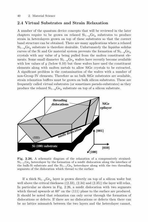
40 2. Material Science
2.4 Virtual Substrates and Strain Relaxation
A number of the quantum device concepts that will be reviewed in the laterchapters require to be grown on relaxed Si1−yGey substrates to producestrain in heterolayers grown on top of these substrates so that the correctband structure can be obtained. There are many applications where a relaxedSi1−yGey substrate is therefore desirable. Unfortunately the liquidus soliduscurves of the Si and Ge material system prevents the formation of Si1−yGey
crystals with any value of y being pulled from the molten constituent ele-ments. Some small diameter Si1−yGey wafers have recently become availablewith low values of y (below 0.10) but these wafers have used the constituentelements along with molten metals to allow SiGe crystals to be extracted.A significant problem is the contamination of the wafers with a number ofnon-Group IV elements. Therefore as no bulk SiGe substrates are available,strain relaxation buffers must be grown on bulk silicon substrates. These arefrequently called virtual substrates (or sometimes pseudo-substrates) as theyproduce the relaxed Si1−yGey substrate on top of a silicon substrate.
(111) misfit dislocation
threadingdislocations
Si (100) substrate
SiGeepilayer
[100]
[001]
[010]
Fig. 2.26. A schematic diagram of the relaxation of a compressively strained-Si1−xGey heterolayer by the formation of a misfit dislocation along the interface ofthe bulk-Si substrate and the Si1−xGey heterolayer along with the two threadingsegments of the dislocation which thread to the surface
If a thick Si1−yGey layer is grown directly on top of a silicon wafer butwell above the critical thickness ((2.33), (2.34) and (2.35)) the layer will relax.In particular as shown in Fig. 2.26, a misfit dislocation with two segmentswhich thread upwards at 60 on the (111) plane to the surface are produced.It should be noted that relaxation can only occur through the formation ofdislocations or defects. If there are no dislocations or defects then there canbe no lattice mismatch between the two layers and the heterolayer cannot,
2.4 Virtual Substrates and Strain Relaxation 41
therefore, be relaxed. The problem with this technique is that a large numberof dislocations are created which interact and penetrate through the epilayerresulting in threading dislocation densities of over 109 cm−2 and frequently1012 cm−2 for the useful Ge contents for devices. This density is significantlyhigher than that which can be tolerated by any electronic or optoelectronicdevice as the dislocations can either trap or interact with the electrons andholes. The problem with this particular technique is that misfit segments nu-cleate at the silicon / Si1−xGex interface and glide along the 111 planesresulting in line vectors along the [110] and [110] directions (Fig. 2.26). Asall the dislocations nucleate at this one interface, there are substantial in-teractions between the two networks of dislocations which impedes the glideof the threading segments to the edges of the wafer. Therefore shorter misfitsegments result which produces a higher density of threading dislocationssince the end of the misfit segment has to be connected to a free surfacevia a threading dislocation. The only other option is the formation of a loopdislocation where the two threading segments join.
One solution to the high dislocation density is to find a method of extend-ing the misfit segment lengths. The ideal scenario is where the two threadshave glided to the edge of the wafer so that they cannot interfere with theactive epitaxial layers grown above the buffer. Three conditions are requiredto extend the misfit segment lengths: (a) The growth temperature or anysubsequent anneal temperature requires to be high enough to enable a high
misfit dislocation velocity (∝ constant × exp[−(
2.25 (eV)kBT
)]), much higher
than the growth rate. (b) Secondly the density of pinning centres or inter-actions with other dislocation threads which result in pinning require to below enough to promote long misfit segments. (c) Third, misfit nucleation isrequired for strain relaxation but the activation energy requires to be higherthan that for dislocation glide.
A number of different approaches have been used to achieve the abovecriteria. One of the first and still to a large extent the most successful is toslowly grade the Ge content from 0% up to the required Ge composition. Thistechnique works very well for Ge contents up to approximately 30% usingconventional CVD or MBE growth techniques provided the grading rate isbelow 10% Ge per µm. Figure 2.27 shows a scanning optical micrograph ofthe surface of a wafer grown at 560 C with a grading rate of 52% per µm.The corresponding transmission electron microscope (TEM) image is shownin Fig. 2.28. The surface is quite clearly pitted even though no threadingsegments can be observed to thread through the surface of the wafer in thecross sectional TEM image. The TEM image also demonstrates that some ofthe 60 C dislocations thread down into the substrate as well as up to thesurface.
If the grading is reduced to 5% per µm with the growth temperature in-creased to 800 C then the surface is substantially improved as demonstratedin Figure 2.29. Comparison of the TEM picture in Fig. 2.30 with that of the

42 2. Material Science
Fig. 2.27. A scanning optical microscope image of the surface of a virtual substrategrown at 560 oC using LPCVD with a Ge grading rate of 52% per µm up toSi0.74Ge0.26
Fig. 2.28. A transmission electron microscope image of the surface of a virtualsubstrate grown at 560 oC using LPCVD with a Ge grading rate of 52% per µmup to Si0.74Ge0.26

2.4 Virtual Substrates and Strain Relaxation 43
Fig. 2.29. A scanning optical microscope image of the surface of a virtual substrategrown at 800 C using LPCVD with a Ge grading rate of 5% per µm
Fig. 2.30. A transmission electron microscope image of the surface of a virtualsubstrate grown at 800 C using LPCVD with a Ge grading rate of 5% per µm

44 2. Material Science
higher grading rate (Fig. 2.28) demonstrates how the dislocation segmentsand visible threads are spread out in the vertical direction resulting in fewerthreading segments vertically. Close inspection demonstrates the reduced in-teraction between the dislocations with the lower grading rate. While theseinteractions are difficult to image using cross sectional TEM, the surface qual-ity of the wafer strongly depends on the number of interactions (Figs. 2.27and 2.29). Low temperature electrical measurements of modulation-dopedstrained-Si quantum wells grown on top of the buffers also demonstrate thedifference in virtual substrate quality. The 52% per µm buffer had a 1.5 KHall mobility of 128 000 cm2/Vs while the 5% per µm substrate had a Hallmobility of 258 000 cm2/Vs. The active heterolayers in this case were grownat 560 C after the high temperature buffer had been completed.
At low growth temperatures (irrespective of the grading rate), a smallnumber of heterogeneous dislocation nucleation sources are activated result-ing in large dislocation pileups containing a particular Burgers vector. Thesepileups give rise to a large spread of mosaic crystal tilts relative to the sili-con substrate. The size of these dislocation pileups may be correlated withthe surface roughness measured by atomic force microscopy (AFM). At highgrowth temperatures, more dislocation nucleation sources are activated andthe pileup size and hence the spread in mosaic crystal tilts is reduced. In bothcases the presence of these dislocation pileups controls the surface morphol-ogy although through different mechanisms. Large pileups of 60 dislocationsresult in a tilting of the surface at low growth temperatures because of thesurface disruption caused by the tilt component of the dislocation’s Burgersvector. At higher growth temperatures this effect is reduced and as the pileupsize is reduced the surface morphology is dominated by strain driven rough-ening due to the residual strain field around the dislocation pileups and theincreased surface mobility afforded by higher temperature growth due to dif-ferent surface energies of the heteromaterials. The origins of these rougheningmechanisms are found to occur during the very earliest stages of relaxationsuggesting that it is this part of the growth which must be controlled toremove these effects.
Table 2.8 provides a summary of different virtual substrate growth tem-peratures along with grading rates and thicknesses of the constant composi-tion buffer above the grading region. 1.5 K mobilities have also been providedwhere n-type modulation-doped structures have been grown on top with astrained-Si quantum well. The sample with the lowest electron mobility hasthe thinnest top constant composition buffer. This sample actually has alower mobility than growth of a single constant composition buffer withoutany grading which has a dislocation density above 1011 cm−2. Therefore inthe thin constant composition buffer sample, the misfit segments are fre-quently within 100 nm of the electrons in the quantum well and the mobilityis reduced due to strong interactions with the dislocations. Increasing thethickness of this buffer to over 0.6 µm can remove most of this interaction,

2.4 Virtual Substrates and Strain Relaxation 45
thereby significantly increasing the mobility. This is probably due to the mis-fit dislocations trapping charge and it is the interaction of this charge throughremote Coulomb scattering which is detrimental to the mobility.
Table 2.8. A comparison of the grading rate, growth temperature and thicknessof the constant composition layer of different strain relaxation buffer grown byLPCVD, solid source MBE and LEPECVD. Root mean squared (rms) rough-ness values have been measured by AFM while mobility measurements are forn-MODFETs except the final row which is a p-type Ge channel MODFET withmobility measured at 4.2 K.
growth growth final grade constant rms 1.5Ksystem temp. Ge rate comp. roughness mobility
(oC) comp. (%Ge/µm) thickness (nm) (cm2/Vs)(µm)
LPCVD 800 28 % 45 0.33 20-25 -LPCVD 800 27 % 42 0.33 23-25 -LPCVD 560 29 % 36 0.09 2-3 2,390LPCVD 560 26 % 52 0.87 3-4 137,000LPCVD 800 23 % 7 0.68 2 133,000LPCVD 800 24 % 5 0.88 2 258,000MBE 450 30 % single step 0.5 13,100MBE 750 25 % 30 0.58 88,500MBE 750 29 % 8.5 0.6 173,000LEPECVD 720 35 % 5.8 1.8 <1 150,000LEPECVD 720 70 % 10 1.5 4.5 87,000 (p)
The results in table 2.8 demonstrate that relatively high electron mobili-ties can still be achieved even with aggressive grading rates. The thickness ofthe constant composition buffer is far more important to distance the elec-trons from the misfit segments. The best mobilities at low temperatures canonly be achieved by grading at less than about 10% per µm and for these n-types modulation-doped samples the Ge content requires to be between about20 and 30 %. As virtual substrates are grown with the same techniques above30 % Ge content, the surface roughness of the buffers is increased and thegrading rate becomes more important for high mobility.
Low energy plasma enhanced CVD has been developed specifically to growthick relaxed buffer layers at high growth rates and low Ge grading per µmto reduce the surface roughness and threading dislocation density especiallyfor Ge contents above 30 %. Growth rates up to 7 nm per second have beendemonstrated and the material has demonstrated very high mobilities bothat room and low-temperatures. A significant problem with these thick virtualsubstrates is that the thermal conductivity of SiGe layers is significantly lowerthan bulk silicon or bulk germanium (Si0.8Ge0.2 has a thermal conductivity of5.1 Wm−1K−1 compared to Si of 140 Wm−1K−1 and 70 Wm−1K−1 for Ge).This is a serious issue for a number of electronic and optoelectronic deviceapplications where the ability to remove the power which is dissipated as heat

46 2. Material Science
is paramount. Therefore there has been a significant interest in developingthin virtual substrate techniques both to reduce the thermal problems butalso to reduce the fabrication time and hence cost of virtual substrates.
A number of alternative techniques for thin virtual substrates have alsobeen researched or are presently being developed. The first of these usedsilicon-on-insulator (SOI) substrates as a base where the buried oxide is usedas a compliant layer. A pseudomorphic Si1−xGex layer is grown at low tem-perature above the top silicon layer of the SOI substrate. Once the Si1−xGex
is deposited, the whole wafer is annealled at high temperatures so that theSi1−xGex layer relaxes on the compliant oxide layer.
A second technique uses point-defects (vacancies, interstitials) producedeither by growth at very low temperature (150C-400C) or by ion bombard-ment. If there are a large number of point defects close together then thepoint defects can condense and form prismatic dislocation loops which sup-ports the relaxation without threading segments through the surface of theheterolayer. There can also be interaction of the point defects with the dis-locations. Such interactions allow dislocation climb as well as the previouslydiscussed glide along the [110] directions which can lead to the annihilationof defects. High Ge content up to 50%, high degree of relaxation up to 100%and cross-hatch free surfaces have been demonstrated with sub 100nm virtualsubstrates, while supersaturation of point-defects and micro twins formationare remaining problems.
A similar techniques for virtual substrates was demonstrated using hy-drogen ion implantation a process which has similarities to the SmartCutTM
silicon-on-insulator (SOI) technique. The hydrogen implantation into a pseu-domorphic Si1−xGex layer is used to produce a thin defect band slightlybelow the Si1−xGex / Si interface. During subsequent annealling, plateletsand cavities form giving rise to strongly enhanced strain relaxation. Initialexperiments demonstrated a reduced threading dislocation density comparedto relaxed constant composition layers. It has been suggested that the defectband induces stain relaxation via preferred nucleation of dislocation loops inthe defect band which extend to the interface to form misfit segments.
The latest technology that has emerged especially for strained-Si CMOSis strained-Si on insulator which is similar to SOI. For MOSFETs with chan-nel lengths below about 30 nm partially or fully depleted SOI devices may berequired to allow MOSFETs to be switched off with a low enough off-currentfor circuit applications. CMOS microprocessors using SOI wafers are alreadyin production as the reduced capacitance from the buried oxide improvesthe circuit performance by up to 30 % compared to a bulk silicon substrate.As strained-Si CMOS gets closer to production SOI versions of the technol-ogy are likely to be developed. There have been a number of demonstrationsof strained-Si directly on the oxide which remains stable up to anneal tem-peratures of 950 oC. Both wafer bonding and oxide implantation (SIMOX)techniques have been demonstrated. Strained-Si CMOS devices have been

2.5 Further Reading 47
produced on both types of SOI wafers with enhanced performance over stan-dard bulk Si and SOI substrates.
From the materials side of silicon and silicon-germanium technology, vir-tual substrate development is one of the most active research areas at presentas many different device technologies require a relaxed Si1−yGey substrate. Itis highly likely that there will be new developments in this area in the futureas the buffers as such an important part of quantum devices.
2.5 Further Reading
1. J. Murota, B. Tillack, M. Caymax, J. Sturm, Y. Yasuda, S. Zaima ,Proc. First Internat. SiGe Technology and Device Meeting, Appl. Surf.Sci., Vol. 224 (2004)
2. R. Waser, Nanoelectronics and Information Technology, Wiley-VCH,Weinheim (2003)
3. C.K. Maiti, N.B. Chakrabarti, S.K. Ray, Strained Silicon Heterostruc-tures Materials and Devices, The Institution of Electrical Engineers, Lon-don (2001)
4. E. Kapser and K. Lyutovich, Properties of Silicon Germanium andSiGe:Carbon, EMIS Datareviews, Vol.24, INSPEC, London (2000)
5. M.A. Herman and H. Sitter, Molecular Beam Epitaxy: Fundamentals andCurrent Status, 2nd Edition, Springer-Verlag, Berlin (1996)
6. J.F.A. Nijs, Advanced Silicon and Semiconducting Silicon-Alloy BasedMaterials and Devices, IOP publishing, Bristol (1994)
7. F. Schaeffler, Semicond. Sci. Technol. 12, 1515 (1997)8. E. Kasper, K. Lyutovich, Solid-State Electronics 48, 1257 (2004)

3. Resume of Semiconductor Physics
This chapter presents a brief summary of the physics required to understandthe operation of the devices presented in later chapters. It is not the intenthere to provide a complete volume on the whole of semiconductor physics andit is assumed that the reader already has a basis in solid state theory andquantum mechanics. The reader seeking further information should consultone of the many text books covering the areas in this chapter in more detail.
3.1 Quantum Mechanics
3.1.1 The Wave Behaviour of Particles
It was originally de Broglie who suggested that particles such as electronscould have wave behaviour and defined the de Broglie wavelength, λ for aparticle of momentum, p to be
λ =h
p(3.1)
where h is Planck’s constant. Therefore, an electron in a vacuum at positionr without any external forces could be described by a state or wavefunction,ψ (r) which is a form of a travelling wave such that
ψ (r) = exp [i (k · r− ωt)] (3.2)
This describes the motion of the wave at time, t with angular frequency, ωand wavevector, k such that
k = |k| =2π
λ(3.3)
The complete description of the wave behaviour of electrons is describedby the Schrodinger equation. For this chapter it will be the single-particle,time independent Schrodinger equation which is required and is defined inthe general case as
Hψ (r) = Eψ (r) (3.4)

50 3. Resume of Semiconductor Physics
where H is the Hamiltonian operator of the system. From (3.1), the momen-tum in quantum mechanics can be written as
p =h
λ= h
k2π
= hk (3.5)
where h = h2π . From this the momentum operator, p can be defined such
that
pψ (r) = −ih∇ψ (r) (3.6)
Since classically kinetic energy of a particle with velocity, v and mass, mis given by
12mv2 =
(mv)2
2m=
p2
2m(3.7)
the quantum mechanical analogy defines the operator for kinetic energy as
p2
2mψ (r) = − h2
2m∇2ψ (r) (3.8)
and combining this with the potential energy in the system, V (r) gives thesingle-particle, time independent Schrodinger equation as
− h2
2m∇2ψ (r) + V (r)ψ (r) = Eψ (r) (3.9)
It is the solutions to this equation which will allow the physics behind theelectrons in semiconductors to be understood.
The other major piece of quantum mechanics required for this chapteris that due to Planck who postulated that atoms in the walls of a cavityemitted radiation in quanta. A few years later, Einstein concluded that elec-tromagnetic radiation of frequency, ν behaved as if it consisted of a collectionof energy quanta with energy hν. These quanta are now called photons andbehave with Bose-Einstein statisics such that the energy of each photon is
E = hν = hω =hc
λ(3.10)
where ω is the angular frequency which equals 2πν.
3.1.2 The Potential Barrierand Quantum Mechanical Tunnelling
Tunnelling is a purely quantum mechanical effect with no similar effect inclassical mechanics. If a particle is incident on a potential barrier of heightV0 then classically if it has energy lower than V0 it is reflected. The particleis only transmitted when it has higher energy than V0 allowing the barrier

3.1 Quantum Mechanics 51
Ec
Ev
strained-Si SiGe strained-SiEg
V0
α exp(-k2z)Energy
z
wavefunction ψ(z)
Incident electronψ(z) = exp(ik1z)
β exp(k2z)
Transmitted electronψ(z) = t exp(ik1z)
Reflected electronψ(z) = r exp(-ik1z)
b2
b20
Region1 Region 2 Region 3
Fig. 3.1. A schematic diagram of a single barrier produced in Si/SiGe heterostruc-tures using relaxed SiGe and strained-Si. The wavefunctions in the three regionsare also drawn along with the appropriate equations
to be surmounted. In the quantum mechanical case, a particle of energy lessthan V0 may tunnel through the barrier.
Figure 3.1 shows the band structure and trial wavefunctions for the caseof a single potential barrier of height V0 and width b created using strained-Si and relaxed SiGe. We will only consider the one dimensional case of anincident electron of kinetic energy E and mass m∗ in the conduction bandincident on the barrier, and ignore the transverse components in the xy-plane.[The effective mass, m∗, in a semiconductor will be defined fully in Sect.3.2.1.] The system is described by the one-dimensional, time independentSchrodinger equation
− h2
2m∗∂2ψ (z)
∂z2+ V (z)ψ (z) = Eψ (z) (3.11)
For electrons of incident energy less than the barrier height, E < V0
Region 1 z < − b
2V (z) = 0
ψ (z) = exp (ik1z) + r exp (−ik1z) k1 =
√2m∗E
h2 (3.12)
representing a normalised incident plane wave solution in addition to a re-flected component of amplitude r and wavenumber k1.
Region 2 − b
2< z <
b
2V (z) = V0
ψ (z) = α exp (−k2z) + β exp (k2z) k2 =
√2m∗ (V0 − E)
h2 (3.13)

52 3. Resume of Semiconductor Physics
which describes an exponentially decaying wavefunction in the barrier whereα is the amplitude of the wave travelling to the right and β is the amplitudeof the wave travelling to the left. k2 is the wavenumber inside the barrier
Region 3 z >b
2V (z) = 0
ψ (z) = t exp (ik1z) k1 =
√2m∗E
h2 (3.14)
which describes a transmitted wave of amplitude t.The value and slope of the wavefunction must be continuous everywhere
and so ψ (z) and dψ(z)dz are matched at the boundaries. To calculate the current
in the system we require to find the flux transmission coefficient T . A wave
F exp (ikz) carries a current density(hk/m∗
) ∣∣∣F ∣∣∣2 and so the transmissioncoefficient is
T =hk1/m∗hk1/m∗
∣∣t∣∣2 =∣∣t∣∣2 (3.15)
One may also define the reflection coefficient, R in a similar manner
R =hk1/m∗hk1/m∗
|r|2 = |r|2 (3.16)
and the conservation of particles produces
T + R = 1 (3.17)
One may solve for t and hence T (E) using the information above and find(V0 > E)
t =2k1k2 exp (−ik1b)
2k1k2 cosh (k2b) − i (k21 − k2
2) sinh (k2b)(3.18)
and
T =4k2
1k22
4k21k
22 + (k2
1 + k22)
2 sinh2 (k2b)
=1[
1 + V 20
4E(V0−E) sinh2 (k2b)] (3.19)
In the approximation k2b 1 (i.e. for a high or wide barrier)
T ≈ 16E (V0 − E)V 2
0
exp (−2k2b) ≈ 16E
V0exp (−2k2b) (3.20)
The important result is that the transmission coefficient decays exponentiallyas the width of the barrier is increased.

3.1 Quantum Mechanics 53
3.1.3 Quantum Wells
Quantum wells play an enormous role in microelectronics and are found inmany different shapes and forms. For many cases explicit solutions existto Schrodinger’s equation and we start by solving the case of a simple onedimensional quantum well of depth V0 and width w (Fig. 3.2(a)). We requireto calculate the energy levels En of a particle in the well of mass m∗. Insidethe well, the potential V (x) is 0 and so the Schrodinger equation takes theform
d2ψ
dx2+ α2ψ = 0 for − w
2≤ x ≤ w
2where α2 =
2m∗Eh2 (3.21)
and outside the well where the potential is V0
d2ψ
dx2−β2ψ = 0 for x < −w
2and x >
w
2β2 =
2m∗ (V0 − E)h2 (3.22)
V
xw2
w2
Vo
x
V
x
V
(a) (b)
(c)(d)
E0
E1
E2
Fig. 3.2. The three major types of quantum wells found in microelectronics: (a)finite square quantum well, (b) parabolic quantum well and (c) triangular quantumwell. (d) shows the wavefunctions of the first three subbands in a finite quantumwell
At an infinite distance from the well, the probablity of finding the particle,|ψ|2 vanishes and so the boundary conditions are:
ψ = A exp [−iβx] for x < −w2 (3.23)

54 3. Resume of Semiconductor Physics
ψ = Aexp [iβx] for x > w2 (3.24)
ψ = Cexp [iαx] + Dexp [−αx] for w2 ≤ x ≤ w
2 (3.25)
where A, B, C and D are integration constants which are bound by the con-tinuity requirements of ψ and dψ
dx at x = ±w2 . The normalised eigenfunctions
may also be written in the form
ψ =
⎧⎨⎩√
2w sin
[nπw x
]with n = even integer√
2w cos
[nπw x
]with n = odd integer
(3.26)
For an infinitely deep quantum well with V0 En, the solutions are
En =(n + 1)2 π2h2
2m∗w2for n = 0, 1, 2, 3, . . . (3.27)
while for a finite well
En =h2
2m∗w2
[π (n + 1) − arcsin
√En/V0
]2
for n = 0, 1, 2, 3, . . .(3.28)
For a parabolic well (Fig. 3.2(b)) with V (x) = 12m∗ω2x2 the eigenfunctions
are
ψn (x) ∼ exp[− x2
2a2
]Hn
(x
a
)with n = 0, 1, 2, 3 . . . (3.29)
where Hn are the Hermite polynomials and a =√
h/m∗ωThe eigenenergies of a parabolic well are given by
En = hω
(n +
12
)with n = 0, 1, 2, 3, . . . (3.30)
For many microelectronic devices, the confining potential for electrons canbe approximated as a triangular well. A triangular well (Fig. 3.2(c)) confinedby an electric field, F corresponding to the potential
V (x) = qFx for x > 0 and (3.31)
V (x) = ∞ for x < 0 (3.32)
and the solutions are given by
ψn (x) = Ai
[(2m∗qF
h2
)1/3(x − En
qF
)](3.33)
where Ai [x] is the Airy’s function. The energies are given by
En ≈(
h2
2m∗
)1/3[3πqF
2
(n +
34
)]2/3
(3.34)

3.1 Quantum Mechanics 55
3.1.4 The Hydrogen Atom
Before considering the electronic band structure of crystals, it is worthwhileconsidering the electronic structure of a simple one electron hydrogen atom.This is the simplest atom to investigate as it is a two particle system with apositive nucleus of mass, m1 at a position, r1 and an electron of mass, m2 atposition r2. The standard method of solving the problem is to transform intothe centre of mass coordinate, R and the difference coordinates, r defined as
R =m1r1 + m2r2
m1 + m2(3.35)
and
r = r1 − r2 (3.36)
along with the reduced mass, mµ
1mµ
=1
m1+
1m2
(3.37)
The solution can be found in any good quantum mechanics text book andis the result of being able to separate the equation into two parts by letting
ψ (r1, r2) = f (R)ψ (r) (3.38)
where
− h2
2M∇2f (R) = EKf (R) (3.39)(
− h2
2mµ∇2 − q2
4πε0r
)ψ (r) = Eψ (r) (3.40)
and the total energy, ET is given by
ET = EK + E (3.41)
The eigenenergy and eigenfunction of the centre of mass part (see (3.39)) aresimply those of a free particle of mass, M with energy
EK =h2K2
2M(3.42)
and
f (R) =exp [iK · R]√
V(3.43)
so that the total solution is given by
ψ (r1, r2) =exp [iK · R]√
Vψ (r) (3.44)

56 3. Resume of Semiconductor Physics
where V is the volume of the space. The solutions of these equations areextremely involved and the reader is refered to a number of quantum me-chanical texts. For the crystal and electronic structure, it is the shape andenergy of the solutions that are important. The solutions are labelled fromthe lowest energy upwards as s-, p-, d-, f-,. . . . For the bandstructure of sili-con, only the s- and p- orbitals need to be considered and the shapes of thesewavefunctions are shown in Fig. 3.3. Each orbital state (s-, p-, d-, f-,. . . ) canonly be occupied by a fixed number of electrons. The s-state can only havetwo electrons and is spherical (Fig. 3.3(a)). The p-states have three differ-ent possible orientations and each can be occupied by 2 electrons. Thereforethe p-states can have a total occupation of six electrons. The d-states canhave up to ten electrons occupying them. The orbitals states also form shells.The inner shell is just an s-state (1s). The second shell can have both sand p-states (2s 2p). The third shell can have s-, p- and d-states (3s 3p 3d)and the fourth can have s-, p-, d- and f- (4s 4p 4d 4d). It is this structurewhich defines the periodic table. The number of electrons in each filled ornon-filled orbital state is normally denoted by a superscript after the shellnumber and orbital letter. Therefore Si with 14 electrons has the electronicconfiguration of 1s22s22p63s23p2 and Ge with 32 electrons has the configura-tion 1s22s22p63s23p63d104s24p2. It is only the electrons in the outer shell orvalence electrons which will be important for electronic properties since theinner shells are strongly bound to the nucleus through the Coulomb force.
x
y
z(a)
s-states
x
y
z(b)
p-states
x
y
z
x
y
z
Fig. 3.3. The probability densities for the s- and p-states of an electron in ahydrogen atom
While these wavefunctions are derived for the hydrogen atom, by replacingthe masses with those for other larger atoms, these solutions are taken as anapproximation to the energy levels for the larger atoms. It is the interactionof these hydrogen-like orbitals which form the bonds between atoms thatcreates molecules and crystals. The Pauli Exclusion Principle states that forfermions such as electrons, only one electron can be in each quantum state orenergy level and so with the spin degeneracy there are two electrons in eachenergy level (one with spin up and the other with spin down). Two electronsare also required to form a covalent bond between atoms to form moleculesor crystals. Through the wave behaviour of the electrons, the wavefunctions

3.2 The Band Structure of Semiconductors 57
for bonds can have a number of positive or negative interference effects whenthe wavefunctions are added. The positive are termed bonds and the negativeare termed antibonds.
In the next section, the electronic structure of a single atom will be ex-panded to that for a crystal structure using a number of different techniques.This will allow the electronic properties of semiconductors to be calculated.
3.2 The Band Structure of Semiconductors
3.2.1 The Free Electron Picture and the Effective Mass
The Schrodinger equation for a free particle in 3D is
− h2
2m∇2ψ (r) = Eψ (r) (3.45)
In orthogonal coordinates, the simplest crystal that the electrons can beconfined to is a cube of edge, L. If we define the origin at one corner of thecube, the wavefunction in the cube must be a standing wave of the form
ψ (r) = A sin(πnxx
L
)sin
(πnyy
L
)sin
(πnzz
L
)(3.46)
where nx, ny and nz are positive integers. It is convenient to introducewavefunctions which satisfy periodic boundary conditions in x−, y− andz−directions with period L. Thus
ψ (x + L, y, z) = ψ (x, y, z) (3.47)ψ (x, y + L, z) = ψ (x, y, z) (3.48)ψ (x, y, z + L) = ψ (x, y, z) (3.49)
Wavefunctions which satisfy the free particle Schrodinger equation and theperiodic boundary equations are of the form of a travelling plane wave suchas
ψ (r) = exp [ik · r] (3.50)
provided that the components of the wavevector k satisfy
kx, ky, kz = 0; ±2π
L; ±4π
L; . . . (3.51)
The components of k are the quantum numbers for the problem alongwith the quantum number for electron spin in the system, ms.
On substituting (3.50) into (3.45), the energy of the electrons for awavevector k is

58 3. Resume of Semiconductor Physics
E =h2k2
2m(3.52)
remembering that m is the mass of the electron in vacuum. In reality theelectron does not behave as if it is in a vacuum and the free electron picturebasically replaces the mass of the electron in vacuum by an “effective mass”,m∗ which accounts for the interactions that the electron feels in the crystal byusing the mass as an empirical fitting parameter. This technique works quiteeffectively for simple parabolic bands and for small applied electric fields. Inreal semiconductors, the bands can be quite complicated and the effectivemass may be anisotropic. This difference in the mass of the electron shouldnot be too surprising as the transport is by waves through the crystal ratherthan particles in a vacuum in the free electron picture. The next section willderive the effective mass by comparison of the quantum mechanical picturewith classical mechanics which will allow a more general definition of theeffective mass.
If the momentum operator p = hi ∇ is used on the wavefunction ψ then
pψ (r) =h
i∇ψ (r) = hkψ (r) (3.53)
The plane wave function of the electron is therefore an eigenfunction of thelinear momentum with the eigenvalue hk. Relating this crystal momentumwith the classical momentum produces
m∗v = hk (3.54)
Now since the group velocity of a wave is related to the angular frequencyof the wave, ω and from Planck’s quantisation of energy E = hω
v =∂ω
∂k=
1h
∂E
∂k=
h
2m∗∂
∂kk2
=hkm∗ (3.55)
While (3.54) suggests by comparison that the semi-classical particle ve-locity of the electron equals the crystal momentum divided by the effectivemass, (3.55) shows how the group velocity of the electron wave is equal tothe crystal momentum divided by the effective mass. If this is now put intoNewton’s law relating the electric field, F to the velocity of an electron ofcharge q then
qF = −m∗∂v∂t
= −m∗ ∂v∂k
∂k∂t
=m∗
h2
∂2E
∂k2· qF (3.56)
Now (3.56) suggests that the effective mass can be defined by
1m∗ =
1h2
∂2E
∂k2(3.57)
and therefore may be obtained from the energy dispersion relation or bandstructure of the isotropic material. More generally the effective mass isanisotropic in many crystals and has therefore tensor properties.

3.2 The Band Structure of Semiconductors 59
1m∗
ij
=∂2E
∂pi∂pj=
1h2
∂2E (k)∂ki∂kj
(3.58)
There are more complete descriptions of the effective mass such as thatdefined in k.p-theory (Sect. 3.2.6) which calculates an effective mass whichtakes into account mixing from different bands which are interacting. Thiswill be briefly introduced in section 3.2.6 but is well beyond the scope of thepresent text. The major point is that the effective mass is a useful constructthat naively determines the amount of interaction a conduction electron in acrystal has with the lattice and other electrons in the system.
3.2.2 The Crystal Structure
All major semiconductors which are used in manufacturing such as Si, Ge orGaAs are crystalline materials. Each has a regular structure of the constituentatoms along with a lattice constant.
By defining the basis vectors a, b and c describing a crystal solid suchthat the crystal structure remains invariant under translation through anyvector that is an integer multiple of the basis vectors, the direct lattice sitesr can be defined as:
r = ia + jb + kc (3.59)
(for i, j, k = integers).At room temperature and pressure, the group IV elements of Si and Ge
both form the diamond lattice structure. Each of the four electrons in theouter shell form sp3 hybridised orbitals with covalent bonds between theatoms being formed by one electron from each atom with opposite spin. Thesp3 hybridised orbitals produce the tetrahedral structure which creates theface centred cubic diamond lattice (Fig. 3.4). The structure results in the111 planes being the easiest cleavage planes for both Si and Ge.
For a given set of direct basis vectors, a set of reciprocal lattice vectorsa∗, b∗, c∗ can be defined such that
a∗ ≡ 2πb × c
a ∗ b× c(3.60)
b∗ ≡ 2πc × a
a ∗ b × c(3.61)
c∗ ≡ 2πa × b
a ∗ b× c(3.62)
so that the reciprocal lattice point is given by
r∗ = la∗ + mb∗ + nc∗ (3.63)
(for l, m, n = integers)

60 3. Resume of Semiconductor Physics
Ge
Sia a
Diamond Zinc Blend
Fig. 3.4. (a) The diamond crystal structure of elemental Si and Ge. The zinc blendstructure is that found for compound semiconductors such as GaAs and orderedSi0.5Ge0.5
Γ
L
XK W
Σ∆
Λ U
Fig. 3.5. The body centred cubic reciprocal lattice along with the Brillouin zoneboundaries and the major symmetry points marked on the using the standard grouptheory symbols
The unit cell of the reciprocal lattice can be formed by constructing theWigner-Seitz cell. The Wigner-Seitz cell is primitive and displays the sym-metry of the crystal system. To obtain this cell one must start at any of thelattice points and the origin and draw vectors to all the neighbouring latticepoints. Planes perpendicular to and passing through the midpoints of thesevectors are constructed. The Wigner-Seitz cell is then the smallest volumeabout the origin bounded by these planes.
For a face centred cubic lattice, the reciprocal lattice which forms theWigner-Seitz cell is a body centred cubic lattice. Figure 3.5 shows the bodycentred cubic reciprocal lattice along with the corresponding Brillouin zoneboundaries with the major symmetry points marked by the standard grouptheory symbols. Once the crystal structure of a material is known, this fre-quently allows the calculation of the energy band structure from Schrodinger’sequation to be simplified when the symmetry of the system is taken into ac-count.

3.2 The Band Structure of Semiconductors 61
3.2.3 Bloch’s Theorem and Bloch Functions
For a periodic potential, the electronic band structure and the wavefunctionsare derived from the Hamiltonian which must satisfy the symmetry of thecrystal. For an electron in a periodic potential, V
V (r) = V (r + r) (3.64)
where r = n1a + n2b + n3c and a, b and c are the lattice basis states andn1, n2 and n3 are integers. This translation is therefore just a translation bya lattice vector or multiples thereof. The electron wavefunction, as before,must satisfy the Schrodinger equation
Hψ (r) =[− h2
2m∗∇2 + V (r)]
ψ (r) = E (k)ψ (r) (3.65)
The Hamiltonian must be invariant under translation by the lattice vectorr → r+r. If ψ (r) is a solution to (3.65) then so must be ψ (r + r). Thusψ (r + r) can only differ from ψ (r) by at most a constant. This constantmust have a unity magnitude otherwise the wavefunction will grow to infinityif the translation r is repeated indefinitely. Therefore the general solutionto Schrodinger’s equation must be of the form
ψnk (r) = exp [ik · r] unk (r) (3.66)
where unk is defined as the periodic function
unk (r + r) = unk (r) (3.67)
This result is Bloch’s theorem and the wavefunctions, ψnk (r) definedin (3.66) are called Bloch functions. It is important to note that Bloch’stheory is a result of the crystal lattice periodicity and not related to quantummechanical effects.
3.2.4 The Kronig-Penney Model
The simplest periodic array to consider is that of a set of square well po-tentials. In modern semiconductor systems this can be grown epitaxially andis called a superlattice. The system is also appropriate for considering a 1Dmodel of electrons travelling through a crystal in that the electron experi-ences a periodic potential due to the crystal structure. Each electron will beaccelerated as it approaches the positive nucleus of each atom and then adecceleration as it moves past before experiencing the acceleration from thenext atom. The starting point is to approximate the crystal by assuming thateach loosely bound valence electron in the outer shell of an atom is confinedby the positive nuclear charge to a square potential well

62 3. Resume of Semiconductor Physics
–b a
Vo
V
xa+b0
Fig. 3.6. The periodic potential which is used in the Kronig-Penney model
The solutions for a single quantum well have already been calculated inSect. 3.1.3. For the present case the solutions can be divided into the quantumwell and the barrier (Fig. 3.6) so that we have respectively
ψ (x) = A exp [iαx] + B exp [−iαx] for 0 < x < a (3.68)ψ (x) = C exp [iβx] + D exp [−iβx] for −b < x < 0 (3.69)
with
α2 =2m0E
h2 ; β2 =2m0 (E − V0)
h2 (3.70)
The solutions require to be periodic and therefore we require the solutionsto have a Bloch form. Thus the solution in the region a < x < a + b must berelated to the solution in the barrier (equation 3.69) in the region −b < x < 0by the Bloch theorem so that
ψ (a < x < a + b) = ψ (−b < x < 0) exp [ikx (a + b)] (3.71)
which naturely defines the wavevector, kx as an index for the solution. Asbefore for the quantum well, the constants A, B, C and D must be chosenso that ψ and dψ
dx are continuous at x = 0 and x = a. At x = 0
A + B = C + D (3.72)iα (A − B) = iβ (C − D) (3.73)
At x = a by applying equation 3.71 for ψ (a) under the barrier in terms ofψ (−b)
A exp [iαa] + B exp [−iαa] = (3.74)(C exp [−iβb] + D exp [iβb]) exp [ik (a + b)]
iα (A exp [iαa] − B exp [−iαa]) = (3.75)iβ (C exp [−iβb] − D exp [iβb]) exp [ikx (a + b)]

3.2 The Band Structure of Semiconductors 63
-2
0
2
4
6
8
-4π -3π -2π -π 0 π 2π 3π 4π
αa
forbidden region
forbidden region
Allowedsolutions
π αasi
n[αa
]+co
s[αa
]
Fig. 3.7. A plot of the left-hand side function from (3.77) with β2ba2
= π. Theallowed values of energy of an electron in the system is related to the values of αawhich lie between ±1 on the vertical axis since the right-hand side of (3.77) is acosine function. Outside this range, no Bloch or travelling wave solutions can exist.Therefore a number of forbidden energy gaps are created
The solution to set of equations (3.72) to (3.76) can be found only if thecoefficients to A, B, C and D can be made to vanish. For E < V0, β∗ = iβ,it can be shown with much algebra that this is when(
β∗2 − α2
2αβ∗
)sinh [β∗b] sin [αa]+cosh [β∗b] cos [αa] = cos [kx (a + b)](3.76)
A much simpler result can be found if the periodic potential is replacedby a set of δ-functions so that (3.76) is being taken in the limit of b = 0and V0 → ∞. In this limit β∗ α and β∗b 1 which allows (3.76) to besimplified to(
β∗2ba2
)sin [αa]
αa+ cos [αa] = cos [ka] (3.77)
This equation does not have solutions for all α. As an example, if we setβ∗2ba
2 = π, then Fig. 3.7 shows the solutions plotted. The only allowed valuesof energy are for which the left-hand side of (3.7) exists for real k. Sincethe right-hand side is a cosine function, which can only have values ±1, anysolutions outside ±1 are not allowed and energy gaps form. The energy as afunction of k is plotted in Fig. 3.8. The energy is parabolic when averaged

64 3. Resume of Semiconductor Physics
over the whole dispersion curve but energy gaps open up at values of k = nπa
where n is an integer. While the curves can be plotted over all k, since thestructure is periodic, the solutions are typically folded back into ±nπ
a whichis called the reduced zone scheme (Fig. 3.8(b)).
k
E(k)
2pa
pa
2pa
pa 0
E(k)
pa
pa 0
(a) (b)
energygap
energy gap energy gap
energygap
Fig. 3.8. (a) A plot of energy against wavenumber in the extended zone schemefor the Kronig-Penney potential demonstrating the energy gaps at kx = nπ
awith n
and integer. (b) A plot of the same potential as (a) but in the reduced zone scheme
These energy gaps open up in any 1D system such as a superlattice andare useful in designing a number of quantum devices since electrons can onlyhave a certain energy and are forbidden to have energies corresponding tothose in the band gaps. The origin of these gaps is from the periodicity ofthe crystal structure and the wave behaviour of the electrons. In the nextsections, the band structure for bulk 3D crystals such as Si and Ge will becalculated where again band gaps will form due to the periodicity of thematerial.
3.2.5 The Tight Binding Model
There are two different starting points for calculating the band structure ofmaterials. Either the starting point is from isolated atoms being put togetherinto a crystal with the individual wavefunctions of the atoms overlapping toform bands (e.g. the Kronig-Penney model in 1D, Sect. 3.2.4) or you startfrom a large bulk crystal and use the periodicity and wave properties ofelectrons through Bloch’s theory to find the band structure. In this section,the tight binding method will be shown to be the former by constructing theband structure from the energy structure of the constituent atoms.
We have already found the molecular orbitals for the hydrogen atom,Sect. 3.1.4. It will become important for the tight binding method but also
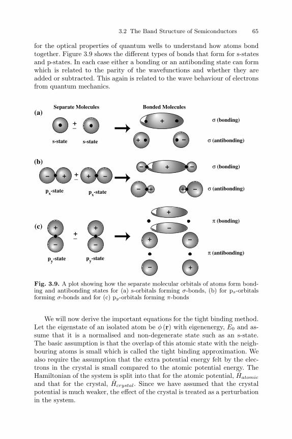
3.2 The Band Structure of Semiconductors 65
for the optical properties of quantum wells to understand how atoms bondtogether. Figure 3.9 shows the different types of bonds that form for s-statesand p-states. In each case either a bonding or an antibonding state can formwhich is related to the parity of the wavefunctions and whether they areadded or subtracted. This again is related to the wave behaviour of electronsfrom quantum mechanics.
(a)
s-state s-state
+_
+_
(b)
– + + –+– –
– + –+
+_(c)
–
+
–
+
–
+ –
+
Separate Molecules
px-state px-state
py-state py-state
Bonded Molecules
σ (bonding)
σ (antibonding)
σ (antibonding)
π (antibonding)
σ (bonding)
π (bonding)
+
–
–+
+
Fig. 3.9. A plot showing how the separate molecular orbitals of atoms form bond-ing and antibonding states for (a) s-orbitals forming σ-bonds, (b) for px-orbitalsforming σ-bonds and for (c) py-orbitals forming π-bonds
We will now derive the important equations for the tight binding method.Let the eigenstate of an isolated atom be φ (r) with eigenenergy, E0 and as-sume that it is a normalised and non-degenerate state such as an s-state.The basic assumption is that the overlap of this atomic state with the neigh-bouring atoms is small which is called the tight binding approximation. Wealso require the assumption that the extra potential energy felt by the elec-trons in the crystal is small compared to the atomic potential energy. TheHamiltonian of the system is split into that for the atomic potential, Hatomic
and that for the crystal, Hcrystal. Since we have assumed that the crystalpotential is much weaker, the effect of the crystal is treated as a perturbationin the system.

66 3. Resume of Semiconductor Physics
If we now define the atoms as sitting on the lattice points, rm then whenan electron is close to the atom at rm = 0 its eigenfunction is approximatelyφ (r). Similarly when the electron is near the atom at the lattice point rm,its wavefunction is approximately φ (r − rm). Thus the wavefunction for oneelectron in the crystal is
ψk (r) =∑m
Akmφ (r− rm) (3.78)
The summation must be over all the lattice points in the system. This wave-function is a linear combination of atomic orbitals (LCAO) and the techniqueis sometimes named LCAO rather than tight binding. This wavefunction mustbe of a Bloch form and so for N atoms in the crystal, let
Akm =1√N
exp [i (k.rm)] (3.79)
and the wavefunction for tight binding becomes
ψk (r) =1√N
∑m
exp [i (k.rm′)] φ (r− rm) (3.80)
It is easy to show that this wavefunction satisfies Bloch’s theorem byreplacing r with r + ∆r and showing that
ψ (r + ∆r) = exp [i (k.∆r)]ψ (r) (3.81)
While (3.80) can be used to calculate the band structure for differentmaterials, this is a whole field unto itself and for the purposes of this text itis important only to understand how the method is derived and used alongwith the results from the technique. Figure 3.10 shows how the bands in aparticular crystal system form from the molecular orbitals as a function ofthe spacing of the atoms. At infinite seperation the atoms have the hydrogenlike molecular orbitals and as the atoms are brought together in a crystaland bonds are formed between molecules, bands of allowed energies for theelectrons to occupy form. On paper one can bring the nuclei together but thisis not a useful concept as it cannot be done in real crystals. The importantpoint for the crystal is when the distance between atoms corresponds to thelattice spacing of the crystal. In the particular case shown in Fig. 3.10, twobands with a band gap between them are formed. This particular diagram isappropriate for the case of Si.
The actual band states that are formed for Si and for Ge are shown inFig. 3.11. As will be derived later in a rigourous manner, the Fermi energyseparates the filled from the unfilled states and for pure crystals lies inside aband gap. It is this band gap that defines a semiconductor. Insulators havevery large band gaps and it is impossible to excite carriers across it at roomtemperature. Hence electrons have no free states to occupy and no electronictransport can take place. In metals the bands all overlap and electrons at

3.2 The Band Structure of Semiconductors 67
atomic separation
Energy
a0
3s
3p
Fig. 3.10. The formation of the band structure as isolated atoms with s- andp-states are brought together. For the case of silicon the s- and p-levels form sp3
hybridised orbitals separated by an energy gap
a finite temperature can always move to a free state in another band andso the electrons can easily move around and hence they have good electricaltransport properties. Semimetals such as graphite also exist where the filledand unfilled bands touch and so are insulators at 0 K but metals at all finitetemperatures. Semiconductors lie between semimetals and insulators in thatthe band gaps are small enough that at a high enough temperature, elec-trons can be excited across the band gap into free states allowing electronictransport.
(a) (b)
3p
3s
s antibonding
p antibonding
p bonding
s bonding
s antibonding
p antibonding
p bonding
s bonding
4p
4s
EF EF
Fig. 3.11. The formation of the band structures of (a) Si and (b) Ge from thevalence electrons in the outer shell of each atom

68 3. Resume of Semiconductor Physics
The top of the filled electron band is called the valence band (Ev) whilethe bottom of the unfilled states is termed the conduction band (Ec). ForSi both of these have p-state characteristics while for Ge, the bottom of theconduction band has s-state characteristics. The complete band structure formaterials is normally calculated using k.p theory or pseudopotentials so thecomplete band structure of semiconductors will be left to the next section.
3.2.6 Pseudopotentials and k.p Theory
Most band structures that are used for semiconductors are the ones calcu-lated using the pseudopotential model. While such modelling is well beyondthe level of the present text, it is informative to at least have a conceptualidea of how such band structures are calculated particularly since the pseu-dopotential band structures will be the ones typically used to explain theproperties of almost all bulk semiconductors.
The pseudopotential relies on splitting the potential of an atom into twoseparate parts: one for the electrons closest to the core of the atom and asecond for the valence electrons in the atom. Therefore the pseudopotentialreproduces the valence states as the lowest eigenstates of the problem andneglects the core states. From chemistry and the concept of bonding withvalence electrons (see Sect. 3.2.5) this is not too difficult to justify. The mainreason for this division from the band structrue calculation point of view isthat the wavefunctions of the electrons near the core of the atom will havestrong spacial oscillations which makes it very difficult to solve Schrodinger’sequation for the system. The pseudopotential technique relys on the splittingof the potential for the atom into a part for the valence electrons and a softpotential part for the core. This allows Schrodinger’s equation to be solved bysplitting it into the parts of the core and the valence electrons. A summationof Bloch-like plane waves are used for the valence electron wavefunctionswhich are modified by making them orthogonal to the core-level states. Thisresults in the potential having the required soft core. The typical type ofpotential is shown in Fig. 3.12.
In the k.p method the band structure over the entire Brillouin zone can beextrapolated from the zone centre energy gaps and optical matrix elements.The k.p method is therefore extremely convenient for interpreting opticalspectra from semiconductors and heterostructures. The technique is also use-ful for strained materials as the strain can be calculated as a perturbation tothe system. The technique allows the band dispersion and effective masses tobe calculated around high symmetry points.
The k.p method can be drived from the one-electron Schrodinger equation(3.9) by applying Bloch’s theorem. Using a Bloch wavefunction of the form
ψnk (r) = exp [i (k.r)] unk (r) (3.82)

3.2 The Band Structure of Semiconductors 69
Ionpotential~–1/r
coreregion
V(r)
r
~1/2 bond length
Fig. 3.12. The typical pseudopotenial for a Si atom in real space. The solid curvein which V (r) →= 0 in the core region is called a ‘’soft core” pseudopotential. Thedashed curve in which V (r) → constant is a ‘’hard core” pseudopotential
where n is the band index, k lies within the first Brillouin zone and unk isa function with the periodicy of the lattice. Substituting (3.82) into (3.9)produces(
p2
2m0+
hk.pm0
+h2k2
2m0+ V (r)
)unk (r) = Enkunk (r) (3.83)
where m0 is the free electron mass. At k = (0, 0, 0) this reduces to(p2
2m0+ V (r)
)un0 (r) = En0un0 (r) (3.84)
While (3.83) could be solved for any k-point, the advantage of solving at(0,0,0) is that the functions of unk are then periodic. Therefore once En0 andun0 are known, the terms hk.p/m0 and h2k2/ (2m0) are pertubations andcan be calulated using degenerate or non-degenerate perturbation theory. Itshould be noted that since the perturbations are proportional to k and k2,this method works best for small values of k.
As an example, let us calculate using non-degenerate perturbation theorythe first terms at least to second order for a band structure which has anextremum at the energy, En0.
unk (r) = un0 (r) +h
m0
∑n′ =n
〈un0 (r)| k.p |un′0 (r)〉En0 − En′0
un′0 (r) (3.85)
and
Enk = En0 +h2k2
2m0+
h2
m20
∑n′ =n
|〈un0 (r)| k.p |un′0 (r)〉|2En0 − En′0
(3.86)

70 3. Resume of Semiconductor Physics
The linear term in k vanishes because En0 has assumed to be an ex-tremum. If the energy is rewritten for small values of k as
Enk = En0 +h2k2
2m∗ (3.87)
then the effective mass, m∗ is brought into the method but with the definition
1m∗ =
1m0
+2
m∗0k
2
∑n′ =n
|〈un0 (r)| k.p |un′0 (r)〉|2En0 − En′0
(3.88)
This provides a clearer picture of the concept of the effective mass as itdefines, m∗ in terms of the coupling between electronic states in differentbands through the k.p term. The change in value from the free electronmass is therefore defined in terms of a perturbation to the electron from theelectronic states in the system.
3.2.7 Bandstructures of Real Materials
In this section the band structures of Si, Ge and GaAs as calculated bypseudopotentials will be reviewed. The simplest case to consider first is GaAswhere the top of the valence band is at the zone centre or Γ (Fig. 3.13).Therefore at k = 0 electrons and holes can either be excited by the absorptionof a photon or a photon may be emitted by the recombination of electron-hole pairs. Therefore GaAs is used in optoelectronics particularly for lightemitting diodes (LEDs) and lasers.
The Si band structure differs from GaAs in a number of ways. Firstly themaximum of the valence band is at k = 0 but the minimum of the conductionband is at approximately 0.85 of the way to the X-point. Si is therefore anindirect bandgap material and as such for an electron and hole pair to begenerated or recombined, a change of k and therefore crystal momentum isrequired. Such a process requires a phonon which is the quantum of heat or alattice vibration and will be reviewed in Sect. 3.6. The other major differenceis that the bottom of the conduction band has six equivalent points as shownin Fig. 3.15 (b) due to the symmetry of the crystal structure. GaAs has onlyone due to the bottom of the conduction band being at k = 0. These sixequivalent points are called valleys.
Ge has a different band structure (Fig. 3.16). Again the top of the valenceband is at k = 0 but this time the bottom of the conduction band is at theL-point. Due to the symmetry this has 8 equivalent directions in reciprocalspace at the Brillouin zone boundary as shown in Fig. 3.15. Therefore Ge haseight half equivalent valleys.
The top of the valence band has much finer structure which is shownin Fig. 3.17. As will be shown in the next section (3.3.2), the valence bandis filled with electrons but some of these can be excited out of the valenceband leaving holes behind. Three seperate bands are found close to the Γ

3.3 The Concentration of Carriers in a Semiconductor 71
Fig. 3.13. The band structure of GaAs calculated using pseudopotentials (afterCohen and Cheklovsky)
point where k = 0, two of which are degenerate in energy. These are calledthe heavy hole and light hole bands and each has a different effective massthrough the different band curvatures. The third band is termed the spinorbit split-off band and is lower in energy than the other two.
3.3 The Concentration of Carriers in a Semiconductor
3.3.1 The Density of States
The density of states, g(E) is defined as the density of allowed energy statesper unit volume and, as will be demonstrated later, is an important numberfor calculating the number of electrons or holes in a semiconductor. A secondway of writing this definition is such that g(E)dE is the number of solutionsto Schrodinger’s equation in the energy interval between E and E + dE. Thedensity of states has different forms depending on the number of dimensionsin the system. If we consider a phase space in d dimensions then statisticalmechanics states that a hyper-volume V in the phase space contains N dis-

72 3. Resume of Semiconductor Physics
Fig. 3.14. The band structure of Si calculated using a simple local pseudopoten-tial (dotted line) and using a non-local pseudopotential (solid line) which moreaccurately reproduces the lowest valence band (after Cohen and Cheklovsky).
[001]
[100]
[010]
[111]---
(c) Ge
[001]
[100]
[010]
(b) Si(a) GaAs
Fig. 3.15. The shape of the conduction band valleys in (a) GaAs, (b) Si and (c)Ge
tinct states where for particles with spin degeneracy gs and valley degeneracygv
N =gsgvV
d
(2πh)d(3.89)
[001]
[100]
[010]

3.3 The Concentration of Carriers in a Semiconductor 73
Fig. 3.16. The band structure of Ge as calculated by pseudopotentials (after Cohenand Cheklovsky)
Ek
heavy holes
light holes
split-off holes
mHH
mLH
mSOH
*
*
*
Ev
Fig. 3.17. A schematic diagram of the top of the valence band. The light hole (LH)and heavy hole (HH) bands are degenerate at k = 0 while the spin orbit split-offband is lower in energy. Each band has a different effective mass due to the differentband curvatures

74 3. Resume of Semiconductor Physics
For a free electron gas, the energy dispersion relation is isotropic E =p2/2m∗ and therefore counting the states in a spherical energy shell dE =(2E/m∗)1/2dp
1D : dN =gsgvLdp
2πh=[gsgv
√m∗
2πh√
2E
]LdE g1D =
gsgv
√m∗
2πh√
2E(3.90)
2D : dN =gsgvL
22πpdp
(2πh)2=[gsgvm
∗
2πh2
]L2dE g2D =
gsgvm∗
2πh2 (3.91)
3D : dN =gsgvL
34πp2dp
(2πh)3=
[gsgv (2m∗)3/2
4π2h3
]L3dE
g3D =gsgv (2m∗)3/2 √E
4π2h3 (3.92)
For both Si and GaAs, the spin degeneracy gs = 2 while for bulk threedimensional Si with the six equivalent valleys, gv = 6. For two-dimensionalquantum wells in silicon such as in the MOSFET (see Sect. 5.3), the quan-tisation in the quantum well (Sect. 3.1.3) can split the valley degeneracysince there will be different subband states with either the longitudinal ortransverse m∗. Therefore gv = 2 is frequently used in 2D layers such as theinversion layer of a MOSFET (Sect. 5). Also if strain is present then thenumber of equivalent valleys can be reduced to either gv = 4 for compressivestrain or gv = 2 for tensile strained layers (see Chap. 4). GaAs with a singlevalley has gv = 1.
3.3.2 Equilibrium Carrier Statistics and Doping
As already described, a pure semiconductor material at 0 K is an insulator.The reason semiconductors are the ideal material for electronics is that byintroducting certain impurities, the conductivity of the material may be con-trollably varied by over 8 orders of magnitude as in Fig. 3.18. For Si or Ge, byintroducting a group V impurity such as As into the host lattice, an electronfrom the As has five valence electrons in the outer shell (Fig. 3.19). Four arerequired for bonding to the host lattice leaving a single free electron. This isthe idea of doping: by introducting impurities a number of extra electrons orholes may be introduced into the system which provide electrical conduction(Fig. 3.19).
Carrier Statistics and Intrinsic Material. At equilibrium, the availablestates in a conductor are filled up according to the Fermi-Dirac distributionfunction which is
f(E) =1
1 + exp[
E−EF
kBT
] (3.93)

3.3 The Concentration of Carriers in a Semiconductor 75
104
103
102
101
100
10-1
10-2
10-3
10-4
1012 1013 1014 1015 1016 1017 1018 1019 1020 1021
Impurity concentration (cm-3)
p-type (B)
n-type (P)
Silicon300 K
Res
isti
vity
(W
-cm
)
Fig. 3.18. The resistivity of n and p-doped Si as a function of doping density (afterSze)
Si Si Si
Si
SiSiSi
SiSi
Si Si Si
Si
SiSiSi
P+Si
Si Si Si
Si
SiSiSi
B-Siq+
q-
Fig. 3.19. Electrical conduction in semiconductors using the s−p3 bonding picture.(a) Intrinsic silicon has no free electrons and is an insulator. (b) P doped materialhas a free electron for each P atom and hence is n-type. (c) B doped material hasan electron missing from a bond and hence is p-type
where kB is the Boltzmann constant, T is the absolute temperature and EF
is the Fermi energy. The Fermi energy, EF is defined as the energy which sep-arates the filled from the unfilled states and is strictly speaking only definedat T =0K. At T=0K, the chemical potential = EF but at finite tempera-tures the two values may differ substantially depending on the system andany applied voltages. Here we will ignore the differences and call both theFermi energy although one should remember that at finite temperatures youare really dealing with the chemical potential. Away from equilibrium, suchas when a bias is applied across a sample, the system has no common Fermienergy but a local Fermi level is defined which can vary spacially in the sys-tem. The Fermi energy is the energy at which the probability of occupation

76 3. Resume of Semiconductor Physics
of a state is precisely one-half. The Fermi-Dirac function is plotted in Fig.3.20 as a function of temperature.
f(E
)
E _ EF (eV)
0K100K
200K300K
400K500K
600K
0
0.2
0.4
0.6
0.8
1
-0.4 -0.3 -0.2 -0.1 0 0.1 0.2 0.3 0.4
Fig. 3.20. The Fermi-Dirac distribution as a function of temperature
There are two limits in which the Fermi function can be simplified. Thefirst is the non-degenerate limit at high temperatures
[E − EF ] >> kBT f(E) ≈ exp[− (E − EF )
kBT
](3.94)
while for the degenerate limit at low temperatures
[E − EF ] << kBT f(E) ≈ Θ (EF − E) (3.95)
where θ is the Heaviside step function which is defined as 0 for EF < E and1 for EF > E.
To calculate the number of carriers in any semiconductor system, thedensity of states multiplied by the Fermi-Dirac distribution is integrated overappropriate limits, i.e.
n =
∞∫0
g(E)f(E)dE (3.96)
For an intrinsic semiconductor without any dopants or impurities com-pared to the number of thermally generated carriers there are few electronsin the conduction band even though there are a large number of allowedstates, hence the probability of an electron populating one of these states is

3.3 The Concentration of Carriers in a Semiconductor 77
small. All the electrons fill the allowed states in the valence band as shownin Fig. 3.21(a). The Fermi level is therefore at the centre of the bandgap andEF Ei (Fig. 3.21(c)) and the number of electrons in the conduction bandequals the number of holes in the valence band (Fig. 3.21(d)).
Ec
Ev
n
p
Ei
E
g(E)
E E
f(E)0 0.5 1
E
n(E) and p(E)
EF
Ec
Evp
n
(a) (b) (c) (d)
np=ni2
Fig. 3.21. A schematic digram of an intrinsic semiconductor (a) The electron andhole distribution in the conduction and valence bands (b) the density of states (c)the Fermi-Dirac distribution with the Fermi energy marked and (d) the number ofelectrons and holes in the structure
To calculate the electron density in a piece of bulk, intrinsic silicon, equa-tions 3.92 and 3.94 must be substituted into (3.96) with a spin degeneracyof 2 and a valley degeneracy of gv giving
n = 4πgv
[2m∗
e
h2
]3/2∞∫0
E1/2 exp−E − EF
kBT
dE (3.97)
To solve this integral, a substitution of x = E/kBT into (3.97) produces
n = 4πgv
[2m∗
ekBT
h2
]3/2
exp
EF
kBT
∞∫0
x1/2exp [−x]dE (3.98)
where∞∫0
x1/2 exp [−x]dE is a standard integral which equals
√π/2. Therefore
n = 2gv
[2πm∗
ekBT
h2
]3/2exp
EF
kBT
(3.99)
Up to now we have been integrating from 0 to infinity but electrons canonly occupy the conduction band. Therefore it is more common to redefinethe electron density with respect to the bottom of the conduction band ratherthan E = 0. This results in (3.99) becoming

78 3. Resume of Semiconductor Physics
n = 2gv
[2πm∗
ekBT
h2
]3/2
exp−Ec − EF
kBT
(3.100)
= NC exp−Ec − EF
kBT
where
NC = 2gv
(2πm∗
ekBT
h2
)3/2(3.101)
is the effective density of states in the conduction band. The reader shouldnote that often the valley degeneracy is combined with the electron ef-fective mass, m∗
e for a new quantity called the effective density of states,m∗
de3/2 = gvm
∗e3/2. In this book we will use the definition given in (3.101)
and previous equations in this section as it is more appropriate for strainedmaterials where the degeneracy is determined by the strain and dimension-ality (i.e. quantisation) of the system. In a similar fashion the hole density inthe valence band may be obtained
p = NV exp−EF − EV
kBT
(3.102)
with the effective density of states in the valence band of
NV = 2(
2πm∗pkBT
h2
)3/2(3.103)
The effective masses in the above equations are the density of states ef-fective masses which nievely take an average value of the masses in all thebands used for conduction. The electron value is defined as
m∗e = (m∗
1m∗2m
∗3)
13 (3.104)
where m∗1, m∗
2 and m∗3 are the effective masses along the three principal axes
of the ellipsoidal energy surface. In silicon (Fig. 3.15) thiscorresponds to
m∗e =
(m∗
l m∗2t
) 13 (3.105)
where m∗l is the longitudinal mass (= 0.916m0) and m∗
t is the transversemass (= 0.19m0). For holes in Si, Ge or GaAs the density of states effectivemass for the valence band is given by
m∗p =
(m
∗ 32
LH + m∗ 3
2HH
) 23
(3.106)
where m∗HH is the heavy hole mass and m∗
LH is the light hole mass.

3.3 The Concentration of Carriers in a Semiconductor 79
0.001 0.002 0.003 0.004 0.005 0.006
1018
1016
1014
1012
1010
108
106
104
102
100
1/T (1/K)
n i (
cm-3
)
Ge
Si
GaAs
200 1672503335001000T (K)
Fig. 3.22. The intrinsic carrier density as a function of temperature for Si, Ge andGaAs
As explained before and shown in Fig. 3.21(d), the number of electrons inthe conduction band equals the number of holes in the valence band and thisnumber is called the intrinsic carrier density, ni = n = p. The Fermi levelcan be found by equating (3.100) and (3.102) to give
Ei =EC + EV
2+
kBT
2ln(
NV
NC
)(3.107)
Since at room temperature the temperature-dependent second term ismuch smaller than the bandgap, the intrinsic Fermi level is close to the centreof the bandgap. The intrinsic carrier density is obtained using (3.100), (3.102)and (3.107) and is given by
np = n2i = NCNV exp
(−EC − EV
kBT
)(3.108)
and since Eg = Ec −Ev, the intrinsic carrier density can be written in termsof the bandgap as
ni =√
np =√
NCNV exp[ −Eg
2kBT
](3.109)
Figure 3.22 shows the temperature dependence of the intrinsic carrierconcentration for the three main semiconductors. At high temperatures, the
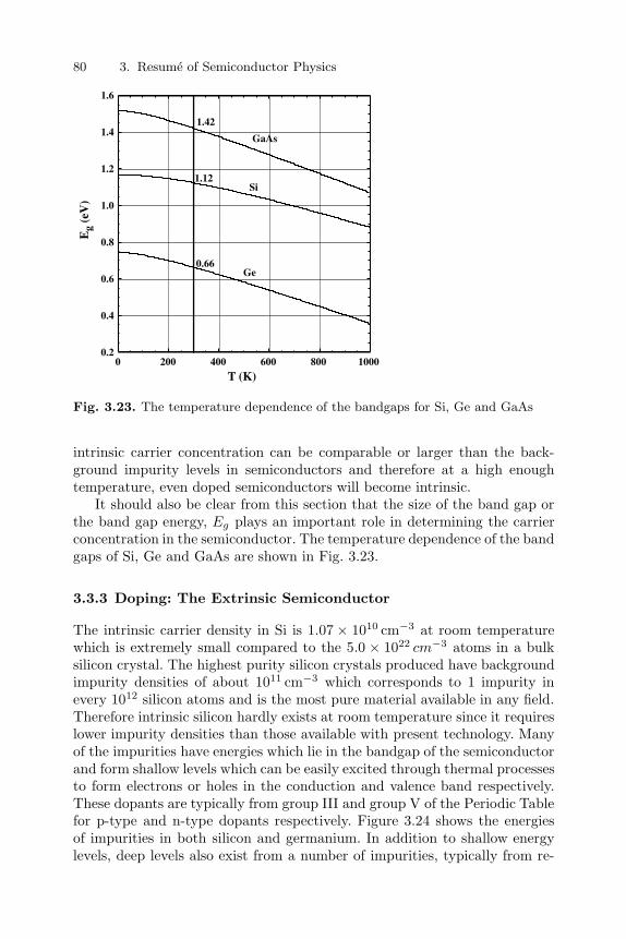
80 3. Resume of Semiconductor Physics
0 200 400 600 800 1000
1.6
1.4
1.2
1.0
0.8
0.6
0.4
0.2
GaAs
Si
Ge
Eg
(eV
)
T (K)
0.66
1.12
1.42
Fig. 3.23. The temperature dependence of the bandgaps for Si, Ge and GaAs
intrinsic carrier concentration can be comparable or larger than the back-ground impurity levels in semiconductors and therefore at a high enoughtemperature, even doped semiconductors will become intrinsic.
It should also be clear from this section that the size of the band gap orthe band gap energy, Eg plays an important role in determining the carrierconcentration in the semiconductor. The temperature dependence of the bandgaps of Si, Ge and GaAs are shown in Fig. 3.23.
3.3.3 Doping: The Extrinsic Semiconductor
The intrinsic carrier density in Si is 1.07 × 1010 cm−3 at room temperaturewhich is extremely small compared to the 5.0 × 1022 cm−3 atoms in a bulksilicon crystal. The highest purity silicon crystals produced have backgroundimpurity densities of about 1011 cm−3 which corresponds to 1 impurity inevery 1012 silicon atoms and is the most pure material available in any field.Therefore intrinsic silicon hardly exists at room temperature since it requireslower impurity densities than those available with present technology. Manyof the impurities have energies which lie in the bandgap of the semiconductorand form shallow levels which can be easily excited through thermal processesto form electrons or holes in the conduction and valence band respectively.These dopants are typically from group III and group V of the Periodic Tablefor p-type and n-type dopants respectively. Figure 3.24 shows the energiesof impurities in both silicon and germanium. In addition to shallow energylevels, deep levels also exist from a number of impurities, typically from re-

3.3 The Concentration of Carriers in a Semiconductor 81
fractory metals. These deep levels are difficult to ionise and therefore may actas traps for carriers in the system, thereby reducing the number of carriersavailable for electronic transport.
Luttinger and Kohn demonstrated that dopant atoms may be modelledusing the modified hydrogen atom to describe the electronic structure ofdopants in semiconductors. The ionisation energy of each dopant is calculatedby replacing the free electron mass with the effective mass and introducingthe dielectric constant, εr of the semiconductor so that the energy of theimpurity in the bandgap is given by
ED =m∗q4
32π2ε20ε
2rh
2 (3.110)
For an intrinsic semiconductor n = p = ni but once dopant impurities havebeen added to a semiconductor, the Fermi level will be adjusted to preservecharge neutrality. If ND donors are added to a system then to preserve chargeneutrality the number of electrons in the conduction band n and the numberof holes in the valence band are related by
n = N+D + p (3.111)
where N+D is the number of ionised donors in the system given by
N+D = ND [1 − f (ED)] = ND
⎡⎣1 − 1
1 + 12 exp
(ED−EF
kBT
)⎤⎦ (3.112)
The 12 in the denominator of f (ED) originates from the spin degeneracy of
the system to allow both up and down spin states. Similarly, if NA acceptorsare added to a semiconductor, the number of ionized acceptors is given by
N−A = NA [f (EA)] = NA
⎡⎣ 1
1 + 12 exp
(EA−EF
kBT
)⎤⎦ (3.113)
For the standard doping species at room temperature in the main semi-conductors, there is very little difference between ND and N+
D . In many casesit is assumed that all the dopants are ionised.
The Fermi level is calculated using (3.111) and substituting in the valuesof (3.100) and (3.102) which gives
NC exp[−Ec − EF
kBT
]=
ND
1 + 2 exp[−ED−EF
kBT
] (3.114)
+ NV exp[−EF − Ev
kBT
]

82
3.
Resu
me
ofSem
iconducto
rP
hysics
Ec
Ev
mid gap
45
B Al Ga In Tl Pd
LiNa Sb P As Bi
24 33 39 45 54 69
67 72160
300 340
Te Ti C Mg Se
Na Be
140210
250
110
250 250
400
Cr Ta Cs Ba S Mn Ag Cd Pt Si
410
140
430
300
500
320
500
260
480
430
530
450
360
330
200
450
550
300
250
360
300
340
490
190
350
420
170
Zn Au Co V Ni Mo Hg Sr Ge Cu K Sn W Pb O Fe
550
260 290
540
350
490
530
400
490
230
350
300
340
330
250
330
360
310
500
280
500
270
240
400
530
350
260
270 310
250
340
370
300220
370
170 160
380
510
410
140
510
400D
D
DD
DDDD
DDD
D
DDD
D
D
A
A
A
A
AA
A A A
A AA
A
Ec
Ev
Li Sb P As
B Al Ga In Be Zn Cr Cd Hg Co Ni Mn Fe Pt
S Se Te Cu Au Ag
10 10
Tl
10 11 11 2060
3595
70
12055
160
87
230
90
250
300A
230
160
300A290A
270A
310
120 A
20040
9.3 9.6 12 13180 140
280
110
300 260A
330
40
40
200A
A
40150
D
28090
130
A
A
Eg =
660 meV
Eg =
1120 meV
mid gap
Germanium
Silicon
Fig
.3.2
4.
The
positio
ns
of
diff
erent
impurities
inth
ebandgaps
of
silicon
and
germ
aniu
m

3.3 The Concentration of Carriers in a Semiconductor 83
which can be solved to find EF in the system. If we consider a n-type semi-conductor then ND NA and the second term in (3.114) can be neglected. Ifwe consider only shallow impurities then at room temperature for moderateconcentrations ND/NC exp [(EC − ED) /kBT ] 1 and therefore
EF∼= Ec − kBT ln
[NC
ND
](3.115)
which on substitution can be rewritten in terms of Ei, ND and ni as
EF∼= Ei + kBT ln
[ND
ni
](3.116)
Ec
Ev
ED
n
p
Ei
E
g(E)
E
ND
E
f(E)0 0.5 1
E
n(E) and p(E)
EF
Ec
Evp
n
(a) (b) (c) (d)
np=ni2
Fig. 3.25. A schematic diagram of (a) the conduction and valence bands of an-type semiconductor with impurity states from dopants in the band gap (b) thedensity of states (c) the Fermi-Dirac distribution and the Fermi energy and (d) thenumber of electrons and holes in the system
All the important parameters discussed above are shown in Fig. 3.25 fora n-type semiconductor. The dopants lie at an energy of ED in the bandgapand hence ND NA. The Fermi level lies close to the conduction band andthe number of electrons in the conduction band is substantially greater thanthe number of holes in the valence band.
The electrons in a n-type semicondutor are the majority carriers but therewill also be holes in the system which are the minority carrier. To find thenumber of holes, (3.100) and (3.102) must be multiplied together to give
np = n2i = NCNV exp
[−Ec − Ev
kBT
]= NCNV exp
[− Eg
kBT
](3.117)
and the hole density is given by
p =n2
i
ND(3.118)
Similar expressions can be obtained for a p-type material where the holes arethe majority carriers and the electrons are the minority carriers.

84 3. Resume of Semiconductor Physics
0 100 200 300 400 500Temperature (K)
0.6
0.4
0.2
0.0
–0.2
–0.4
–0.6
EF
_ E
i (eV
)
Ec
Ev
ND
= 1014
cm-3
1015
1016
1017
1018
1015
1016
1017
1018N
A = 10
14 cm
-3
Fig. 3.26. The variation of the Fermi level in Si for different doping densities anddifferent temperatures (after Grove)
extrinsic region
intrinsicregion
freeze-outregion
ni
ND = 1015 cm-3
Ele
ctro
n de
nsit
y (x
1015
cm
-3)
3.0
2.5
2.0
1.5
1.0
0.5
0.00 100 200 300 400 500 600
Temperature (K)
0 100 200 300–200 –100Temperature (˚C)
ni=nD
Fig. 3.27. The variation of the carrier density in Si as a function of temperaturefor a fixed doping concentration (after Sze)
Figure 3.26 plots the temperature variation of the Fermi level for a num-ber of different doping densities as a function of temperature. As may beobserved, the Fermi level approaches the intrinsic value near the middle ofthe bandgap as the temperature rises. When the intrinsic carrier densitybecomes larger than the doping concentration then the silicon is intrinsic.At the other extreme at very low temperatures, there may not be enoughthermal energy in the system to excite the electron or hole to or from theimpurity state in the bandgap and therefore the number of carriers in thesystem is reduced. This regime is termed the freeze-out regime as eventuallyat 0 K, there will be no carriers in the system since they will all be trappedon the impurity states in the bandgap. The most useful regime is the extrin-

3.3 The Concentration of Carriers in a Semiconductor 85
sic regime which is intermediate to the intrinsic and the freeze-out where allthe donors and acceptors are ionised and the carrier density in the system iscontrolled by the number of dopants. These regimes are shown in Fig. 3.27.
3.3.4 The Two Dimensional Electron Gas (2DEG)
There are two main systems in silicon by which a two dimensional electron gas(2DEG) may be created. The first is an inversion layer as used in the metaloxide semiconductor field effect transistor (MOSFET) where the applicationof a gate bias forms a thin electron layer in the p-type silicon beside anoxide interface, in effect the electric field creates a potential well at the oxideinterface (Fig. 3.28). The second is a modulation doped semiconductor fieldeffect transistor (MODFET) where the dopant atoms are placed a distancefrom a quantum well created by the different bandgaps in two materials andthe electrons (or holes) in the system reside in the quantum well (Fig. 3.28).
Let us consider a quantum well grown in the z -direction so that the x-and y-directions are in the plane of the electron gas. The electrons in either ofthe quantum well systems are described in the effective mass approximationby the Schrodinger equation
− h2
2m∗∇2ψ + Ecψ = Eψ (3.119)
which has solutions of the form
E =h2k2
x
2m∗ +h2k2
y
2m∗ + Ez,n (3.120)
where the nth subband energy Ez,n is given by the solutions given in Sect.3.1.3 for the appropriate shape of the quantum well. If only the lowest sub-band in the system is below the Fermi energy, the device will have a singledynamical 2DEG with subband energy Ez,0. Having calculated Ez,0 from thequantum mechanics, it may be regarded as the effective potential energy ofthe 2DEG and the carrier density n may be calculated from
n2D =
∞∫Ez,0
g2D (E) f (E)dE (3.121)
with g2D the 2D density of states.For both Si and GaAs, the spin degeneracy gs = 2. For GaAs with a single
valley gv = 1. While Si has six equivalent valleys, due to the quantisation inthe quantum well with the longitudinal and transverse m∗ of electrons, onlytwo valleys form the ground state and so the valley degeneracy for a 2DEGis gv = 2. For a compressively strained-Si1−xGex quantum well the groundstate subbands are formed from 4 valleys with the transverse m∗ giving adegeneracy of gv = 4 while for tensile strained-Si or Si1−xGex, the ground

86 3. Resume of Semiconductor Physics
Fig. 3.28. (a) The band structure of a MOSFET with a 2DEG formed by an inver-sion layer on a p-type silicon substrate. (b) A modulation-doped sample with the2DEG formed in a quantum well of strained-Si. The donors are spacially separatedfrom the 2DEG and hence scattering is reduced in the modulation-doped scheme

3.4 Electronic Transport in a Semiconductor 87
state is composed of two valleys with the longitudinal m∗ giving gv = 2. Fora 2DEG with an isotropic spectrum, the sheet electron density is given by
ns =gsgv (EF − E0)m∗
2πh2 (3.122)
while the Fermi surface is a circle of radius
kF =√
4πns
gsgv(3.123)
3.4 Electronic Transport in a Semiconductor
3.4.1 The Drift Current
In this section we investigate the effects of electric fields on carriers in asemiconductor. As a small electric field, F is applied to carriers, the carrierswill drift in the field with a drift velocity defined as vd. It should be noted thatgenerally both the electric field and the drift velocity are vector quantities butcommonly the basis states are chosen so that only a 1D problem is requiredto be solved and only one component is used. To relate the drift velocity tothe electric field, the common approach is that due to Drude which statesthat in the steady-state, the rate at which electron receive momentum fromthe external electric field is equal to the rate at which the electrons losemomentum due to scattering forces.
dm∗vd
dt
∣∣∣∣scattering
=dm∗vd
dt
∣∣∣∣field
(3.124)
Therefore by defining a momentum relaxation time, τm which is the meantime between scattering collisions (which may be due to scattering from thelattice, impurities, other carriers, phonons, etc. (see Fig. 3.29(b)) the forceon an electron balances as
m∗vd
τm= qF ⇒ vd =
qτm
m∗ F (3.125)
The mobility (sometimes called the drift mobility) is defined as the ratioof the drift velocity to the applied electric field such that
µn =∣∣∣vd
F
∣∣∣ =qτm
m∗ (3.126)
Hence the mobility is a crude measure of the scattering processes in a semicon-ductor which prevent the carriers from accelerating indefinitely (Fig. 3.29(b)).It is clear that carriers have higher drift velocities in high mobility materialsand hence there is great interest in high mobility semiconductors as electronsare transported across the device faster and the transit time of the device

88 3. Resume of Semiconductor Physics
EcEF
Ei
Ev
EcEF
Ei
Ev
electron
hole
V
F=eVI
E
x
n-Si n-Si
eV
vd
Fig. 3.29. A schematic diagram of a n-type semiconductor in (a) thermal equilib-rium and (b) the electron transport under an applied electric field, F
is reduced which in a correctly designed transistor producing higher speedswitching. Eventually the velocity saturates when the scattering balances theforce from the electric field.
If we consider a 2D system such as the 2DEG in a MOSFET or MODFETthen the same equations may be considered from the k-space picture of thesemiconductor. Since the quantum mechanical definition of momentum isp = hk, the k-space equivalent of (3.125) is
δk = −qτm
hF (3.127)
For the case of a 2DEG, the Fermi surface which divides the filled from theunfilled states is a circle in k-space (Fig. 3.30). The effect of the electric fieldis to move the Fermi circle by the amount δk in the opposite direction to theapplied field, F (because the electrons have negative charge). This demon-strates that at sufficiently low temperatures it is only electrons within kBT ofthe Fermi circle which contribute to electron transport in the semiconductor.
The current density in the system is defined as
J = nqvd = σnF (3.128)
From these equations the conductivity of electrons is defined as
σn = qnµn =nq2τm
m∗ (3.129)
One may also define the resistivity as
ρn =1σn
(3.130)

3.4 Electronic Transport in a Semiconductor 89
kx
kyqF
δk
equilibriumdistribution
drifteddistribution
Fig. 3.30. A schematic diagram of a 2DEG with a Fermi circle in an applied electricfield, F. The electron drift due to the electric field is related to the movement ofthe Fermi circle by an amount δk
In a measurement it is the conductance or the resistance which is obtained.For a 2D sample of length L and width W , the resistance is related to theresistivity through
R =L
Wρ (3.131)
and in a similar fashion the conductance, G is defined as
G =W
Lσn (3.132)
For the performance of devices, the carrier velocity as a function of electricfield is important. Figure 3.32 shows the velocity-field curves for a number ofsignificant semiconductors. The curve for Si saturates at > 105 Vm−1. In de-tailed studies of mobility, the principal energy loss mechanism for electronsin high electric fields is optical phonon emission (see Sect. 3.6 for a com-plete description of phonons in semiconductors), characterised by an energyEopt ∼ 62 meV and 37 meV for Ge. Assuming this mechanism is efficient,the maximum drift velocity becomes saturated at
vsat =
√8Eopt
3πm∗ (3.133)
In GaAs, the decrease in velocity above 4000V/cm (Fig. 3.32) is explainedby a two valley model. At low electric fields, the electrons reside in the lowervalley with higher mobility while at higher electric fields, the electrons getheated and reside in the upper valley. The negative differential mobility trans-lates into negative differential resistance and may be used to form microwaveoscillators such as Gunn diodes. At very high electric fields, the carriers getsufficient excess energy to generate electron-hole pairs through impact ionisa-tion. The electron therefore acquires enough energy to break a chemical bondand promote an electron from the valence band to the conduction band. Forhigh electric fields dropped over a sufficiently thick piece of semiconductor,this process may multiply and then the process is known as avalanching. It

90 3. Resume of Semiconductor Physics
Satu
rati
on v
eloc
ity
(m s
-1)
Electric Field (V m-1)
Si electrons
Ge electrons
Ge holes
Si holes
104 105 106 107
103
104
105
106
Fig. 3.31. The saturation velocity for both electrons (solid lines) and holes (dashedlines) in silicon and germanium
is equivalent to dielectric breakdown in other situations. In layered semicon-ductor structures, it is sometimes possible to control this avalanche processto form impact ionisation avalanching and transit time (IMPATT) diodes,the most powerful but noisy source of microwaves. Such processes are alsoused to increase the sensitivity of photodiode detectors.
103
104
105
106
104 105 106 107
Electric Field (V/m)
Satu
rati
on v
eloc
ity
(ms–1
)
T = 300 K
GaAs electrons
Si holes
GaAs holes
Sielectrons
Fig. 3.32. The saturation velocity for both electrons (solid lines) and holes (dashedlines) in GaAs compared to Si

3.4 Electronic Transport in a Semiconductor 91
3.4.2 The Diffusion Current and the Einstein Relation
In the previous section the drift current which resulted from an applied elec-tric field was considered. A second way to create a current is from diffusionof charge rather than drift from a field. Diffusion currents are generally notimportant in metals because the conductivity is extremely high and drift dom-inates but in semiconductors the carrier density can be non-uniform makingdiffusion a possible transport mechanism.
n(x)
x
n(-l)n(0)
n(l)
-l 0 l
Fig. 3.33. The electron concentration, n as a function of distance, x in a 1Dsemiconductor
If we have a change in the electron density, n (x) along the length x- ofa n-type semiconductor then if we consider the number of electrons crossingthe plane at x = 0 per unit time, per unit area we can have the randomthermal motion of the carriers creating a current without an applied electricfield. If we define an electron mean free path, which is the average distancean electron travels before being scattered then = vthτm where vth is thethermal velocity. The average rate of electrons per unit area crossing x = 0per unit time depends on those that started at x = − and is
12n (−) vth (3.134)
where the factor 12 results from the fact that half of the electrons travel from
the left and half from the right. The half that travel from the right are
12n () vth (3.135)
so the net flow of electrons from the left to the right is given by
12vth [n (−)− n ()] (3.136)
Applying a Taylor series expansion to the densities at x = ± then the flowbecomes
12vth
([n (0) − dn
dx
]−[n (0) +
dn
dx
])= −vth
dn
dx(3.137)

92 3. Resume of Semiconductor Physics
Since each electron has a charge −q, the particle flow corresponds to a current
Jn = −q flow = qvthdn
dx(3.138)
The diffusion constant for electrons is defined as
Dn = vth (3.139)
Therefore the diffusion current is normally written in the form
Jn = qDndn
dx(3.140)
and in a similar fashion for holes
Jp = −qDpdp
dx(3.141)
where Dn and Dp are the diffusion constants for electrons and holes respec-tively. The diffusion current is therefore proportional to the rate of change ofthe carrier density along a sample which arises due to the random thermalmotion of carriers at finite temperature in a concentration gradient.
Using equipartition of energy, the thermal velocity of electrons at a tem-perature T given by Boltzmann statistics as
12m∗vth =
32kBT (3.142)
If this is substituted into (3.138) and also the definition of mobility (3.126)then the current density can be written as
Jn = q
(kBT
qµn
)dn
dx(3.143)
and on comparision with (3.140) the diffusion constant is also
Dn =(
kBT
q
)µn (3.144)
while for holes
Dp =(
kBT
q
)µp (3.145)
Equations (3.144) and (3.145) are called the Einstein relations.

3.4 Electronic Transport in a Semiconductor 93
3.4.3 The Current-Density Equations
The total current density is the sum of the drift and the diffusion currents.Therefore using (3.128) and (3.140) the total current density is given forelectrons by
Jn = qnµnF + qDndn
dx(3.146)
and for holes
Jp = qpµpF − qDpdp
dx(3.147)
3.4.4 The Hall Effect and Mobility Measurements
The Hall effect involves measuring the conductivity of electrons in a weakmagnetic field and is important as it allows the carrier density and mobilityof a semiconductor material to be accurately measured. Without the magneticfield, the conductivity only gives the mobility and carrier density product.Generally the technique can be used to measure 3D samples but it is mostfrequently used for 2D systems such as the 2DEG or 2DHG in a MOSFETor MODFET structure. Therefore the geometry that is appropriate and theexperimental setup is shown in Fig. 3.34.
Vxx
VVH I
x
yz
Bz
Fx Fy
+
+
+
__
_
Fig. 3.34. A Hall bar geometry device for measuring the carrier density and mo-bility showing the directions of the electric fields and the currents
As has been discussed in the electronic transport section, at steady state,the rate at which the electrons receive momentum from the applied electricfield is equal to the rate at which this momentum is lost due to scattering.Therefore
dm∗vd
dt
∣∣∣∣scattering
=dm∗vd
dt
∣∣∣∣field
(3.148)
which rewritten as the Lorentz force with the momentum relaxation time, τm
is

94 3. Resume of Semiconductor Physics
Force =m∗vd
τm= q [F + vd × B] (3.149)
Strictly speaking the velocity and the electric field can vary in both the x-and y-directions for the 2D sample in Fig. 3.34 as they are vector propertiesand so[ m∗
qτm−B
B m∗qτm
](vx
vy
)=(
Fx
Fy
)(3.150)
where the usual definitions have been used for the x- and y-components of thedrift velocity, v and the electric field, F. The current density is related to thesheet electron density (2D density), ns through the relationship J = qvdns
and so (3.150) becomes[ m∗qτm
−B
B m∗qτm
](Jx/qnsJy/qns
)=(
Fx
Fy
)(3.151)
which when rearranged defines the conductivity tensor, σn through(Fx
Fy
)=
1σn
[1 −µnB
µnB 1
](Jx
Jy
)(3.152)
with µn = qτm/m∗. Since the resistivity tensor, ρ is defined as(Fx
Fy
)=[
ρxx ρxy
ρyx ρyy
](Jx
Jy
)(3.153)
(3.152) produces the relationships
ρxx =1
σxx(3.154)
ρyx = −ρxy =µnB
σxx=
B
qns(3.155)
Therefore the simple Drude model of electron transport shows that thelongitudinal resistance, ρxx of the Hall bar sample is a constant while thetransverse resistivity, ρyx varies linearly with the magnetic field and inverselyas the carrier density in the sample.
In the experimental setup, a current, I is passed along the sample and twoprobes on the one side of the Hall bar are used to measure the longitudinalvoltage, Vxx. Similarly the Hall voltage, VH is measured using two probes oneither side of the Hall bar. If the magnetic field, B is applied in the z-directionthen
ρyx =VH
I(3.156)
and

3.4 Electronic Transport in a Semiconductor 95
ρxx =Vxx
I
W
L(3.157)
where W is the width of the Hall bar and L is the length. By substitutingthe appropriate equations and variables, these equations can be rearrangedto give the sheet carrier density through
1ns
= qdρyx
dB=
q
I
dVH
dB(3.158)
It should be noted that the direction of the Hall voltage changes if holesrather than electrons are used and therefore the Hall effect can also be used todistinguish whether electrons or holes are the majority carrier in the system.The Hall mobility is also obtained as
µH =1
qnsρxx=
I
q
L
nsVxxW(3.159)
The Hall mobility for electrons is related to the drift mobility, µn throughthe Hall scattering factor, r as µn = rµH . In many cases the Hall scatteringfactor is 1 or close to 1. Care must be taken, however, as many authors ignorethe difference and incorrectly quote the Hall mobility as the mobility. Sincethis technique is the most accurate for measuring the carrier density andmobility, it is typically used for characterising new materials.
3.4.5 Poisson’s Equation and Gauss’s Law
Clearly all semiconductors must obey Maxwell’s equations which explain theelectrostatic and electromagnetic properties of materials. One of the mostuseful and most used in semiconductor devices is Poisson’s equation whichallows the charge density in any system to be obtained. Conventionally, theelectrostatic potential, ψi is defined as
ψi = −Ei
q(3.160)
Again the negative sign represents the negative electron charge compared tothe definition of positive charge movement for current. The electric field, Fis the electrostatic force per unit charge and is equal to the change in theelectrostatic potential as
F = −dψi
dx(3.161)
The charge density, ρ (x) is obtained by differentiating (3.161) to obtainPoisson’s equation
d2ψi
dx2= −dF
dx= −ρ (x)
ε0εr(3.162)

96 3. Resume of Semiconductor Physics
where ε0 is the permittivity of free space (ε0 = 8.85× 10⁻¹² Fm−1) and εr isthe dielectric constant of the medium. This is a 1D equation but generally a2D or a 3D equation can be written and solved. The 3D case is given by
∇2 · ψi = −∇ · F = −ρ (x, y, z)ε0εr
(3.163)
By integrating (3.162) we get Gauss’s law which gives
F =1
ε0εr
∫ρ (x) dx =
Q
ε0εr(3.164)
where Q is the total charge in the system.In any semiconductor, charge can be fixed or mobile. The mobile charge is
either electrons or holes with densities n and p respectively. The fixed chargesare the donors and the acceptors with densities of ND and NA. Therefore forany semiconductor Poisson’s equation (3.162) can be rewritten as
d2ψi
dx2= −dF
dx= − q
ε0εr[p (x) − n (x) + ND (x) − NA (x)] (3.165)
If there is no applied electric field (F = 0) then the right hand side of (3.165)is set to zero and the potential is a constant throughout the semiconductor.
3.4.6 Carrier Concentrations
It will become useful when calculating the carrier densities in many devicesto define the carrier density as a function of the electrostatic potential inthe semiconductor. For a n-type semiconductor, (3.116) can be rewritten interms of the electrostatic potential as
|ψF − ψi| =kBT
qln[ND
ni
](3.166)
where ψF = −EF /q is the Fermi potential. A similar expression can bewritten for the holes. (3.100) and (3.102) can also be rewritten in terms ofelectrostatic potentials rather than energies as
n = ni exp[EF − Ei
kBT
]= ni exp
[q (ψi − ψF )
kBT
](3.167)
and
p = ni exp[Ei − EF
kBT
]= ni exp
[q (ψF − ψi)
kBT
](3.168)
These equations are often called the Boltzmann relations and are validfor both n- and p-type semiconductors and for moderate doping levels.

3.5 Low Dimensional Physics: Quantum Wires and Dots 97
3.4.7 The Debye Length
The bands and the intrinsic Fermi level in inhomogeneous semiconductorsusually follow the variations of (3.166). If the doping concentration, however,changes abruptly then the bands may not follow this change as quickly as thedoping profile. This is because the doping profile may be discontinuous whileψi and the first derivatives must be continuous from any thermal diffusioneffects. There is therefore a length scale, called the Debye length, LD whichis the distance over which the bands of a semiconductor respond to a changeof doping of ND for a n-type semiconductor. To obtain this length, (3.167)is substituted into the (3.165) form of Poisson’s equation to give
d2ψi
dx2= − q
ε0εr
[ND (x) − ni exp
(q (ψi − ψF )
kBT
)](3.169)
To find the Debye length, consider an incremental change in the dopingconcentration, ∆ND (x) with respect to an uniform background doping. Thechange in the intrinsic potential, ∆ψi can be found by expanding the expo-nential term in (3.169) and removing the constants which have no spacialvariation.
d2 (∆ψi)dx2
− q2ND
ε0εrkBT∆ψi = − q
ε0εr∆ND (x) (3.170)
This is a second order differential equation with the solution for ∆ψi ofthe form exp (−x/LD) with
LD =
√ε0εrkBT
q2ND(3.171)
While in many conventional electronic devices, such as transistors, the De-bye length is usually much smaller than any lateral device dimensions, whenquantum devices are considered, it may become an important parameter.
3.5 Low Dimensional Physics: Quantum Wires and Dots
3.5.1 Important Length Scales
Up to this point in this chapter, the vast majority of physics described hasbeen aimed either at 3D or 2D systems. While these are the easiest to realiseexperimentally, it is possible to confine electrons to lower dimensions usinga number of different techniques. Techniques include electrostatic confine-ment using gates which realised some of the first 1D transport along withself-organised growth where 0D quantum dots may be formed. Care must betaken in defining the dimensionality of the sample as the length scales for

98 3. Resume of Semiconductor Physics
different phenomena may be substantially different. A good example is dis-ordered transport in narrow 2DEGs at low temperatures where the samplemay be electrically 2D, the weak localisation due to disorder is typically 2Dbut the electron-electron interactions in the system may be 3D since the in-teractions depends on the thermal length which can be very small comparedto the sample. If a sample is made with dimensions, Lx, Ly and Lz then thedimensionality of the system with respect to different transport regimes maybe inferred by comparing the sample dimensions to the various scatteringand characteristic lengths defined below (Fig. 3.35). Three main regimes fora device of length, Lx and width Ly for 2D system exists; the diffusive regimewhere scattering dominates, the quasi-ballistic regime with very few scatter-ing events and the ballistic regime where there is no scattering inside thedevice on average. The forth main transport regime is quantum mechanicaltunnelling through a barrier.
Lx
Diffusive
Quasi-ballistic
Ballistic
Tunnelling
*
* ** *
*
**
* *
** *
***
** *
**
**
* *
** *
* *
* *
*
** *
**
(a)
(b)
(c)
(d)
l
l
l
scatterer
Ly
Fig. 3.35. The electron transport regimes for small mesoscopic devices of length,Lx and width, Ly : (a) the diffusive case where < Ly < Lx, (b) the quasi-ballisticcase where Ly < < Lx, (c) the ballistic case where Ly < Lx < , (d) the quantummechanical tunnelling regime
The distance an electron travels at constant kinetic energy is
lin the inelastic scattering length (3.172)

3.5 Low Dimensional Physics: Quantum Wires and Dots 99
Examples include electron-electron scattering (at low temperature) andelectron-phonon scattering (at higher temperature e.g. room temperature).The distance an electron travels at constant wave vector is
le the elastic scattering length (3.173)
The effects from Coulombic impurity potentials are an example of elasticscattering. The minimum of the elastic and inelastic scattering lengths is
the mean free path (3.174)
In most semiconductor systems, elastic scattering is almost always theshorter length. In 2D this may be approximated by the expression
=µnh
q
√4πn2D
gsgv(3.175)
The distance an electron travels before the phase of the wavefunction islost is
lφ the phase coherence length (3.176)
The relation between a scattering length lx and the equivalent scatteringtime tx are defined through the diffusion constant D by
lx =√
Dτx (3.177)
and the Einstein relation relates the electron (or hole) mobility to the diffu-sion constant at an absolute temperature T as
µn =qDn
kBT(3.178)
In most conduction processes in semiconductors, only electrons close tothe Fermi energy need to be considered for which the relevant length scale isthe Fermi wavelength
λF =2π
kF=√
2π
n2D=
h√2m∗EF
(3.179)
Length scales associated with the physical quantities of temperature, mag-netic and electric field must also be considered. Thermal smearing and theassociated phase randomisation of an electron of the Fermi distribution pro-duces an energy uncertainty of order kBT . This defines
lT =
√Dh
kBT(3.180)
The magnetic field produces the characteristic length scale

100 3. Resume of Semiconductor Physics
lB =
√h
qB(3.181)
while for an electric field F ,
lF =(
Dh
qF
)1/3(3.182)
In the strongly localised regime, the radius of a hydrogen atom
aB =4πε0h
2
q2m0(3.183)
and the effective Bohr radius which is the radial extent of the wavefunctionof a hydrogen atom like donor in a host crystal is
a∗B =
4πε0εrh2
q2m∗ (3.184)
3.5.2 1D Wires
According to Ohm’s law, the conductance of a large sample is given byG = σLy
Lx. If, however, the length of the sample is much shorter than the
mean free path (i.e. Lx - see Fig. 3.35) then it is found that instead ofthe conductance going towards infinity as Lx is increased, the conductancereaches a limiting value. This appears counter intuitive because we have justdescribed a short 1D wire where there is no scattering and hence one mightexpect the wire to have zero resistance. Landauer described the conductanceof such systems in terms of transmission probabilities of mode Tn, such that
G =gsgvq
2
h
N∑n=1
Tn (3.185)
Solving this for a short 1D channel with N 1D subbands such that noscattering on average occurs in the channel (i.e. the channel length )gives
G = gsgvq2
hN (3.186)
This transport has been termed ballistic transport and the ballistic resistanceis therefore quantised in units of q2/
h.

3.6 Lattice Vibrations and Phonons 101
3.6 Lattice Vibrations and Phonons
3.6.1 The Vibrations of a 1D Monatomic Lattice
The way that heat interacts with electrons and a crystal lattice are extremelyimportant in determining the electronic transport in a semiconductor butthese properties also strongly effects the device performance. The heat prop-erties of crystals was not fully understood until the work of Born and vonKarman in 1912. Their model is extremely simple in that it treates the heatin a crystal lattice as the vibrations of the atoms in the lattice which allowsthe problem to be treated as if the atoms are connected by springs.
κ κ κ
xn xn+1 xn+2xn-1
Fig. 3.36. A schematic diagram of a linear chain of atoms coupled together bysprings of spring constant κ and with displacement of the nth atom by xn
The model has the following assumptions:-1. Each atom is located at an equilibrium position.2. Each atom can oscillate about an equilibrium position with the amplitudeof oscillation small compared to the internuclear distance.Since the force in Newton’s laws depends linearly on the displacement, theatoms can therefore be modelled as if they are connected by springs (Fig.3.36). Let the spring constant be κ and only the nearest neighbour interac-tions will be considered. If the displacement of the nth atom is xn then thepotential energy in the system is
E =N∑
n=1
κ
2(xn+1 − xn)2 (3.187)
where there are N atoms in the lattice chain which are a distance a apartwhen the atoms are not moving (i.e. at 0 K). The force in the system is
force = −dE
dx(3.188)

102 3. Resume of Semiconductor Physics
The equation of motion for the atoms is therefore
md2xn
dt2= κ [(xn+1 − xn) − (xn − xn−1)] (3.189)
All N atoms in then lattice have the same equation of motion. Each of theterms on the right-hand side of (3.189) represents the spring interacting withthe atoms on each side of the atom being considered. Since springs oscillate,the obvious solution to try is a wave solution of the form
xn = x exp [i (nqa − ωt)] (3.190)
This corresponds to a wave along the chain of exp [i (nqa)] with amplitude,x, and time dependence, exp [iωt]. Substituting (3.190) into (3.189) gives
−mω2x = κ [exp (iqa) + exp (−iqa) − 2] x (3.191)
The solutions to this equation holds for all x provided
ω = 2√
κ
m
∣∣∣sin qa
2
∣∣∣ (3.192)
w
q
q
pa
2pa
3pa
4pa
1
–1
vg
0 2pa
3pa
4pa
pa
pa–
wmax
(a)
(b)
Fig. 3.37. (a) The dispersion curves of ω versus the wavevector q for longitudi-nal waves along a linear monatomic chain. (b) The group velocity for the linearmonatomic chain of (a)
The dispersion relation is plotted in Fig. 3.37. The points to note are:

3.6 Lattice Vibrations and Phonons 103
1. there is symmetry about q = 0 i.e. −q is equivalent to +q or in otherwords, the waves are identical in both directions.
2. the results repeat with period 2πa .
3. there is a maximum frequency or cut-off frequency above which atomscannot sustain travelling waves.
4. the index n does not appear in the dispersion relation so only q is requiredto find ω.
The group velocity of a wavepacket is given by vg = dωdk and so the value
for the lattice waves between q = 0 and πa is
vg =√
κ
ma cos
(qa
2
)(3.193)
and vg = 0 for q = πa + m2π
a for all integers m.The above solutions are not changed by much if non-nearest neighbour
interactions are also included. Some additional fine structure is obtained butthe periodicity and general properties shown above are retained. With re-gard to the periodicity, all the information required to describe the latticevibrations of the crystal are contained in an interval of q = 2π
a . The firstBrillouin zone of the 1D lattice is therefore used in a similar manner to thatfor electrons and so only values between −π
a ≤ q ≤ πa are plotted.
In the present 1D crystal, there are N atoms with 1 degree of freedomfor longitudinal motion along the 1D chain and therefore N q-values in thiszone. If transverse directions are also included (i.e. a 3D crystal) then thereare 3N degrees of freedom. If the crystal is considered to have rotationalsymmetry like most semiconductors then there are 2 transverse polarisedvibrations which are degenerate. For both of these the ω versus q curves areidentical and these have the same shape as the longitudinal curves shown inFig. 3.37. In a 3D crystal with one atom at each of N lattice points thereare 3N degrees of freedom and 3N q=values which can all be confined to thefirst Brillouin zone with 1 longitudinal and 2 transverse branches.
3.6.2 The 1D Diatomic Chain
If we have a material such as SiGe or GaAs then there are two different masseson the lattice and so the next system to calculate is a 1D lattice with twodifferent masses. The system will be similar to the monatomic chain excepttwo masses, m and M with m < M will be used (Fig. 3.38). The displacementof the smaller masses will be xn and that of the large masses is Xn. Now thelattice spacing a is twice the distance between nearest-neighbour atoms andthe unit cell has 2 atoms. Again let the system have N unit cells so that thepotential energy in the system is
E =N∑
n=1
κ
2(xn − Xn)2 +
κ
2(Xn − xn+1)
2 (3.194)

104 3. Resume of Semiconductor Physics
κ κ κ
Xn xn Xn+1xn-1
κ
xn+1 Xn+2
κ
m m mM M M
Fig. 3.38. A schematic diagram of a linear chain of atoms coupled together bysprings of spring constant κ and with displacement of the nth atom by xn
and in a similar fashion to the single monatomic chain, the equations ofmotion are
md2xn
dt2= κ (Xn + Xn−1 − 2xn) (3.195)
Md2Xn
dt2= κ (xn+1 + xn − 2Xn) (3.196)
Again the solutions to try are travelling waves of the form
xn = x exp [i (2nqa − ωt)] (3.197)Xn = X exp [i ((2n + 1) qa − ωt)] (3.198)
where x and X are the displacement amplitudes for the masses m and M re-spectively. Substituting these equations into (3.195) and (3.196) the solutionsare
−mω2x = κ [X (1 + exp [iqa]) − 2x] (3.199)−Mω2X = κ [x (exp [−iqa] + 1) − 2X ] (3.200)
To solve these simultaneous equations, the determinant of the coefficients ofx and X are required to be set to zero so that∣∣∣∣ mω2 − 2κ κ (1 + exp [−iqa])
κ (1 + exp [iqa]) Mω2 − 2κ
∣∣∣∣ = 0 (3.201)
which when reduced gives
mMω4 − 2κ (m + M)ω2 + 2κ2 (1 − cos qa) = 0 (3.202)
Solving for ω2 gives
ω2 = κm + M
mM± κ
√(m + M
mM
)2
− 2 (1 − cos [qa])mM
(3.203)
The dispersion relation is plotted in Fig. 3.39. The solutions fall into twodifferent branches which are normally named as the optic and the accoustic

3.6 Lattice Vibrations and Phonons 105
( )
ω
2κm
12
( )2κM
12
qpa0
optic
acoustic
Fig. 3.39. (a) The dispersion curves of ω versus the wavevector q for a lineardiatomic chain. The dispersion is split into the optic branch and the acoustic branch
branches with the optic branch having finite values for q = 0 and the accousticbranch being the same as that observed in the 1D monatomic chain.
If there are N primitive unit cells each with z atoms per cell then in 3Dthere are 3zN different modes. This is what you might expect and is verysimilar to the band structure of the electrons in the lattice i.e. the system isvery complicated if you look at individual modes but due to the periodicityin the system, the modes of the system are much more simple. The solutionsto the simple harmonic oscillator are normally termed normal modes. Thenormal modes of the present system are the linear combinations of atomicdisplacements that completely diagonalise the Hamiltonian terms up to atleast the second order displacements. Once the individual modes are known,the Hamiltonian of the whole system is the sum of the individual simpleharmonic Hamiltonians, one for each 3zN normal modes.
Since the wave motion of the lattice vibrations produces a simple harmonicoscillator, the energy of each mode is given by
E =(
nq +12
)hωq where nq = 0, 1, 2, . . . (3.204)
The total energy in the system is the sum of all the individual modes. It isclear from (3.204) that the lattice vibrations of the system are quantised andequally spaced in energy. These lattice quanta are called phonons (named soas to provide a comparison with photons, the quanta of light).
The phonon dispersion relations for real systems can be calculated andalso measured. They are shown for Si, Ge and GaAs in Fig. 3.40. In allcases the phonon spectra are split into longitudinal optic (LO), transverseoptic (TO), longitudinal acoustic (LA) and transverse acoustic (TA). The

106 3. Resume of Semiconductor Physics
optical phonon energy, Eopt at q = 0 is important for a number of transportphenomena and electron scattering process. It is this energy that was usedin Sect. 3.4.1 in the velocity saturation of electrons in semiconductors. Thevalues of Eopt are 62 meV for Si, 37 meV for Ge and 35 meV for GaAs.
TO
LO
Si
LA
TA
LA
TA
LO
TO
Ge
LO
TO
LA
TA
GaAs
0
2
4
6
8
10
12
14
16
Fre
quen
cy (
TH
z)
0 pa 0 p
a 0 pa
Wavenumber, q
60
50
40
30
20
10
0
Energy (m
eV)
Fig. 3.40. The measured phonon spectra along the (100) direction for Si, Ge andGaAs. The phonon spectra are split into longitudinal optic (LO), transverse optic(TO), longitudinal acoustic (LA) and transverse acoustic (TA)
Phonons are bosons and as such obey Bose-Einstein statistics unlike elec-trons which are fermions and obey Fermi-Dirac statistics. Unlike fermionswhich can only singly occupy quantum states, for bosons there is no limit tothe number which can occupy a single quantum states. The thermodynamicaverage occupation number, 〈nq〉 of phonons in the qth mode of a simpleharmonic oscillator in contact with a heat bath at a temperature T is
〈nq〉 =
∞∑n=0
nq exp[−nqhωq
kBT
]∞∑
n=0n exp
[−nqhωq
kBT
] (3.205)
which reduces to
〈nq〉 =1
exp[
hωq
kBT
]− 1
(3.206)

3.7 Optical Properties of Semiconductors 107
This expression is the thermal occupation factor sometimes called the Bose-Einstein factor. It is worthwhile noting that unlike electrons, the number ofphonons in a system is not conserved.
The average thermal energy for phonons in a system, 〈E〉 = 〈nq〉 hωq andis
〈E〉 =hωq[
exp[
hωq
kBT
]− 1
] (3.207)
which is known as Planck’s law and was originally obtained for photons.At very low temperatures when hωq kBT then both 〈E〉 and 〈nq〉 ≡exp
[− hωq
kBT
]. The probability of phonons to be excited is therefore exponen-
tially low at low temperatures. At high temperatures where hωq kBT
〈nq〉 ≈ kBT
hωq(3.208)
〈E〉 = 〈nq〉 hωq ≈ kBT (3.209)
3.7 Optical Properties of Semiconductors
3.7.1 Blackbody Radiation
The simplest way to generate light from any material is to heat the materialto a temperature, T where incandescence light or black body radiation willbe emitted. To find the states available to a thermal photon in a cubic box oflength, L, again periodic boundary conditions are imposed this time on theradiation field so that the wavevector, k is indexed by the integers, nx, ny
and nz such that
k =2π
L(nxa + nyb + nzc) (3.210)
and
k2 =(
2π
L
)2
r2 (3.211)
Provided the box is large enough then the variable, r can be considered tobe continuous. Therefore in terms of the frequency
2π
cν = |k| =
2π
L|r| (3.212)
where c is the speed of light and therefore
|r| =L
cν (3.213)

108 3. Resume of Semiconductor Physics
For the next section the direction of the vectors is not important and onlythe magnitude of the vectors will be used. The total number of states in thevolume V = L3 between r and r + dr is given by the density of states pervolume, N by a spherical shell
V N (r) dr = 2 · 4πr2dr (3.214)= 8πr2dr (3.215)
= 8π
(L
c
)2
ν2 L
cdν (3.216)
= 8πV
c3ν2dν (3.217)
(3.218)
N (ν) =8π
c3ν2dν (3.219)
0 10 20 30 40 50 60 70 80
1.00
0.75
0.50
0.25
0.00
Spec
tral
Lum
ines
cenc
e (a
.u.)
Frequency (THz)
100 K
200 K
300 K
Fig. 3.41. The distribution of the power radiated from a black body emitter forthree different temperatures
The first factor of 2 corresponds to the two possible transverse photonpolarisations that are possible in any isotropic system. The thermal photonenergy per volume, U in the box is then found by multiplying the densityof states by the photon energy hν and the Bose-Einstein distribution for thephoton occupancy of the available states

3.7 Optical Properties of Semiconductors 109
u = hν8π
c3ν2 1
exp[
hνkBT
]− 1
(3.220)
=8πhν3
c3(exp
[hν
kBT
]− 1
) (3.221)
The spectrum of this function is shown for three different temperaturesin Fig. 3.41
3.7.2 Generation and Recombination Processes
As has been suggested already, provided enough thermal energy is appliedto an electron in the valence band of a semiconductor, the electron may beexcited to the conduction band leaving a hole behind in the valence band.The complete description of such phenomena requires time-dependent per-turbation theory and in particular Fermi’s Golden Rule. An electron can alsobe excited from the valence band to the conduction band by absorption of aphoton in direct band gap materials. In indirect band gap materials, however,phonons are also required for the excitation process. The alternative way ofdescribing such processes is in terms of the balance of electrons and holes ina system in equilibrium such that n2
i = np. The generation or recombinationprocess can then be thought of as a non-equilibrium process where n2
i = np.Fermi’s Golden Rule describes the transitions rate, W for a transitions
from an initial state ψi with energy, Ei to a final state ψf with energy, Ef
when a Hamiltonian, H describes the transition. If photons are also includedwith energy, hω then
Wi→f =2π
h
∣∣∣〈ψf | H |ψi〉∣∣∣2 δ (Ef − Ei − hω) (3.222)
+2π
h
∣∣∣〈ψf | H |ψi〉∣∣∣2 δ (Ef − Ei + hω)
Generally the generation and recombination processes can be divided intoradiative and non-radiative. The non-radiative transitions do not involve pho-tons: they may involve the interaction of the electron with phonons or theexchange of energy or momentum with another electron or hole. Both energyand momentum must be conserved in any process to be discussed in thissection with Fermi’s Golden Rule describing the transition. The transitionsmay also be divided into band-to-bound state transitions and band-to-bandtransitions.

110 3. Resume of Semiconductor Physics
3.7.3 Intrinsic Band-to-Band Generation-RecombinationProcesses
Ec
Ev
Ec
Ev
(a) (b)
Fig. 3.42. The energy band diagram for (a) generation and (b) recombination ofan electron-hole pair across the bandgap of a semiconductor
For band-to-band transitions as shown in a schmatic diagram of Fig. 3.42,the rate of recombination for electrons, Rn and holes, Rp is proportional tothe product of the electron, n and hole, p concentrations such that
Rn = Rp = γnp (3.223)
(see Fig. 3.42 (b)) where γ is the capture coefficient and the generation ratefor electrons, Gn or holes, Gp may be written in terms of the emission rate,ε as
Gn = Gp = ε (3.224)
(see Fig. 3.42 (a)) The net recombination rate is
R = Rn − Gn = Rp − Gp = γnp − ε (3.225)
If no electric or optical excitation of carriers is creating an external per-turbation to the system then in thermal equilibrium the net recombinationrate should be zero giving
γn0p0 − ε = 0 (3.226)
where n0 and p0 are the electron and hole concentrations at thermal equilib-rium i.e. n0p0 = n2
i . The net recombination rate can therefore be rewrittenas
R = γ (np − n0p0) (3.227)
If the carrier concentrations for electrons and holes deviate from the equi-librium values by δn and δp respectively,
n = n0 + δn (3.228)p = p0 + δp (3.229)

3.7 Optical Properties of Semiconductors 111
and therefore for low levels of injections (i.e. where δp (n0 + p0)) therecombination rate is
R = γ (n0 + p0) δn =δn
τR(3.230)
where δn = δp since the electrons and holes are created in pairs for interbandtransitions and the recombination lifetime has been defined as
τR =1
γ (n0 + p0)(3.231)
3.7.4 Extrinsic Shockley-Read-Hall Generation-RecombinationProcesses
Ec
Ev
Ec
Ev
(b) (c)Ec
Ev
(a)Ec
Ev
(d)
Et Et Et Et
Fig. 3.43. The energy band diagram for Shockley-Read-Hall generation and re-combination process (a) electron capture, (b) electron emission, (c) hole captureand (d) hole emission
The Shockley-Read-Hall processes are related to the emission or absorp-tion of a phonon in the system and the four basic processes are shown in Fig.3.43
• 1. The first process is electron capture (Fig. 3.43 (a)) where the recombi-nation rate for the electron is proportional to the density of the electronsand the concentration of traps in the band gap, Nt multiplied by the prob-ability that the trap is empty (1 − ft) where ft is the occupation functionof the trap.
Rn = γnnNt (1 − ft) (3.232)
where γn is the capture coefficient for the electrons.• 2. The second process is electron emission (Fig. 3.43 (b)) where the gener-
ation rate of the electron is
Gn = εnNtft (3.233)
where εn is the emission coefficient and Ntft is the density of traps thatare occupied by electrons.

112 3. Resume of Semiconductor Physics
• 3. The third process is hole capture (Fig. 3.43 (c)) where the recombinationrate for holes is given by the capture of holes by occupied traps. Thisnumber is Ntft and
Rp = γppNtft (3.234)
where γp is the capture coefficient for the holes.• 4. The final process is hole emission (Fig. 3.43 (d)) where the generation
rate is proportional to the density of the traps that are empty (i.e. occupiedby holes)
Gp = εpNt (1 − ft) (3.235)
where the emission coefficient for holes is εp.
Since at thermal equilibrium the net recombination and generation ratesare zero, by using the principle of detailed balancing,
Rn − Gn = γnn0Nt (1 − ft0) − εnNtft0 = 0 (3.236)Rp − Gp = γpp0Ntft0 − εpNt (1 − ft0) = 0 (3.237)
Here the values with a 0 subscript refer to the equilibrium values. Therefore
εn = γnn01 − ft0
ft0(3.238)
εp = γpp0ft0
1 − ft0(3.239)
For degenerate semiconductors, the intrinsic concentrations may be replacedby an effective concentration, nie.
The net recombination rate is
Rn − Gn = Rp − Gp =(γnγpnp − εnεp)Nt
γnn + εn + γpp + εp(3.240)
=γnγp
(np − n2
i
)Nt
γn
(n + n0
1−ft0ft0
)+ γp
(p + p0
ft01−ft0
) (3.241)
for e.g. an n-type semiconductor with n0 p, ∆p p, the net recombinationrate, Rn − Gn is roughly given by ∆p/τp, where
τp =1
γpNt(3.242)
τn =1
γnNt(3.243)
which are the lifetimes associated with the holes and electrons respectively.

3.7 Optical Properties of Semiconductors 113
3.7.5 Auger Generation-Recombination Processes
The Auger recombination process involves the transfer of momentum andenergy released by the recombination of an electron-hole pair to anotherparticle (either an electron or hole). Usually the Auger process is importantwhen the carrier concentration is high or the injection level of carriers is high.
Ec
Ev
Ec
Ev
(b) (c)Ec
Ev
(a)Ec
Ev
(d)
Et Et Et EtEt Et Et Et
Fig. 3.44. The energy band diagram for band-to-bound state Auger generation andrecombination process (a) electron capture, (b) electron emission, (c) hole captureand (d) hole emission
The Auger generation and recombination processes need to be dividedinto band-to-bound state transitions and band-to-band state transitions. Thefollowing band-to-bound state transitions are possible:
• 1. Electron capture with the energy released being absorbed by an electronor a hole (Fig. 3.44(a)). The recombination rate requires two capture co-efficients to account for either an electron or hole gaining energy from thereleased energy
Rn = (γnnn + γp
np)nNt (1 − ft) (3.244)
• 2. Electron emission with an energetic electron or hole supplying the energy(Fig. 3.44(b))
Gn = (εnnn + εp
np)Ntft (3.245)
• 3. Hole capture with an electron or hole absorbing the released energy (Fig.3.44(c))
Rp =(γn
p n + γppp)pNtft (3.246)
• 4. Hole emission with an energetic electron or hole supplying the energy(Fig. 3.44(d))
Gp =(εn
pn + εppp)Nt (1 − ft) (3.247)

114 3. Resume of Semiconductor Physics
If all processes for impurity assisted transitions due to thermal, opticaland Auger-impact ionisation mechanisms exists then
γn = γtn + γ0
n + γnnn + γp
np (3.248)εn = εt
n + ε0n + εn
nn + εpnp (3.249)
γp = γtp + γ0
p + γnp n + γp
pp (3.250)
εp = εtp + ε0
p + εnpn + εp
pp (3.251)
The net recombination rate is given by
Rn − Gn = Rp − Gp =γnγpnp − εnεp
γnn + γpp + εn + εpNt (3.252)
Ec
Ev
Ec
Ev
(b) (c)Ec
Ev
(a)Ec
Ev
(d)
Fig. 3.45. The energy band diagram for band-to-band state Auger generation andrecombination process (a) electron capture, (b) electron emission, (c) hole captureand (d) hole emission
For band-to-band Auger-impact ionisation processes, there are again fourdifferent processes.
• 1. Electron capture with an electron in the conduction band recombiningwith a hole in the valence band and a nearby electron absorbing the energy(Fig. 3.45(a)). An electron-hole pair is destroyed by this process.
Rn = γAun n2p (3.253)
• 2. Electron emission with an electron in the valence band being excited tothe conduction band because of impact ionisation of an incident electronin the conduction band which breaks a bond and creates an electron-holepair (Fig. 3.45(b)).
Gn = εAun n (3.254)
• 3. Hole capture where an electron in the conduction band recombines witha hole in the valence band with the released energy absorbed by a nearbyhole destroying an electron-hole pair (Fig. 3.45(c)).
Rp = γAup np2 (3.255)
3.7 Optical Properties of Semiconductors 115
• 4. Hole emission where an electron in the valence band is excited to theconduction band due to the impact of an energetic hole in the valence band(Fig. 3.45(d)). The breaking of a bond to create an electron-hole pair mayalso provide enough energy.
Gp = εAup p (3.256)
Since each process creates or destroys one electron-hole pair, the total netAuger recombination rate is the sum of the net rates for electrons and holes.
R = Rn − Gn + Rp − Gp (3.257)=(γAu
n n + γAup p
) (np − n2
i
)Typical values for the Auger coefficient, γAu
n n in silicon are of the order of 1to 2×10⁻³¹ cm6s−1.
3.7.6 Impact Ionisation Generation-Recombination Processes
The final generation and recombination mechanisms to be considered arethose by impact ionisation which typically occur when high electric fields areinvolved. The process is similar to the reverse Auger processes discussed inthe previous section except the rates depend on the current densities ratherthan the concentrations of carriers. The generation rates for electrons andholes are
Gn = αn|Jn|q
(3.258)
Gp = αp|Jp|q
(3.259)
where αn and αp are the ionisation coefficients for electrons and holes respec-tively. αn is the number of electron-hole pairs generated per unit distance dueto an incident electron.
The total net recombination rate is
R = −Gn − Gp (3.260)
= −αn|Jn|q
− αp|Jp|q
(3.261)
116 3. Resume of Semiconductor Physics
3.8 The Continuity Equations Including Recombinationand Generation
The current densities equations from Sect. 3.4.3 must now be added to thecontinuity equations for a semiconductor to include the generation and re-combination rates so that
∂n
∂t= Gn − Rn +
1q∇ · Jn (3.262)
∂p
∂t= Gp − Rp − 1
q∇ · Jp (3.263)
describes the electrons and holes in a semiconductor where
Jn = qµnnF + qDn∇n (3.264)Jp = qµppF − qDp∇p (3.265)J = Jn + Jp (3.266)
J is the total current in the system. Once the generation and recombinationrates are obtained for the dominant processes (Sect. 3.7), the current densityequations can be applied to any semicoductor structure or device as will beshown in later chapters.
3.9 Further Reading
1. S.L. Chuang, Physics of Optoelectronic Devices, John Wiley and Sons,New York (1995)
2. S. Datta, Electronic Transport in Mesoscopic Systems, CUP, Cambridge(1995)
3. J.H. Davies, The Physics of Low Dimensional Semiconductors, CUP,Cambridge (1998)
4. M.J. Kelly, Low Dimensional Semiconductors: Materials, Physics, Tech-nology, Devices, OUP, Oxford (1995)
5. O. Madelung, Introduction to Solid State Theory, Springer, Berlin (1981)6. K. Seeger, Semiconductor Physics: An Introduction, 6th Edition, Springer,
New York (1997)7. S.M. Sze, The Physics of Semiconductor Devices, 2nd Edition, John Wiley
and Sons, New York (1981)8. S.M. Sze, Semiconductor Devices: Physics and Technology, 2nd Edition,
John Wiley and Sons, New York (2002)

4. Realisation of Potential Barriers
The function of a device is essentially based on internal potential barrierswhich may be modified by external voltages. The traditional way to cre-ate potential barriers is performed by p/n-junctions or metal/ insulator/semiconductor-junctions. The internal barriers created are usually high –inthe order of the band gap–, but distributed across several tenths of nanome-ters to micrometers which is too broad for utilisation of quantum effects.For heterostructures the internal barriers are smaller –several hundreds ofmillivolts–, but confined to –ideally– atomic distances. Quantum device de-signs, therefore, may combine internal barriers created by p/n- and hetero-junctions.
4.1 Depletion layer and built in voltage
The barrier created by a p/n junction will now be derived but a fuller deriva-tion of all the transport properties of a p/n is given in Sect. 5.1. Consider aone sided abrupt junction (Fig. 4.1) between a heavily n-doped side (markedn+) and a p-doped side (marked p). The diffusion across the junction andrecombination of carriers will result in the formation a depletion layer withwidth WD. The depletion region extends mainly in the lower doped partbecause the sum over all charges has to be zero (neutrality).
Fig. 4.1. The depletion layer of width WD at the junction between a high dopedn+−region and a lower doped p−region

118 4. Realisation of Potential Barriers
ND × xn = NA × xp (4.1)
WD = xn + xp∼= xp (4.2)
In our case ND NA, and xp xn.Without any external voltage these sheets of positive (n - side, N+
D - ions)and negative (p - side, N−
A - ions) charges create an electrical field and a builtin potential ψbi the height of which may best be determined by consideringa uniform Fermi energy level at equilibrium (Fig. 4.2). The built in potentialψbi is given by
Fig. 4.2. The band diagram of the p/n-junction of Fig. 4.1. An energy barrierq × ψbi is created in the absence of an external voltage
ψbi = VT ln(
NA × ND
n2i
)(4.3)
with NA, ND doping levels (acceptor, donor), ni intrinsic carrier density(1010 cm−3 for Si, T = 300K), VT = kBT/q thermal voltage (25 mV at roomtemperature). The typical built in voltage is somewhat lower than the bandgap, e.g. around 0.8V – 1V in Si. Application of an external voltage eitherdecreases the potential barrier (ψbi−V) in the forward direction (positivevoltage with voltage reference at the n - side) and increases it in the reversedirection. The corresponding depletion width WD is given by
WD =
√2ε0εr (ψbi − V )
qNA(4.4)
(where ε0 is the permittivity in a vacuum and εr is the relative dielectric con-stant of the material) resulting in the high nonlinear forward characteristicsand the low reverse current of a biased p/n-junction.
Similarly a metal/semiconductor creates a depletion layer and a built inpotential which is determined by the Schottky barrier energy φB and thedoping level ND (n-type semiconductor).
ψbi =φB
q− VT ln
(NC
ND
)(4.5)

4.2 δ-Doping and n-i-p-i Structures 119
(NC conduction band effective density of states).In a metal/insulator/semiconductor structure three regimes can be ob-
served. A depletion layer extends from the insulator/semiconductor inter-face in the bulk for gate voltages between the flat band voltage, VFB , andthe threshold voltage, VT . Beyond the threshold voltage the depletion layerextension stops and a minority carrier inversion channel adds to the inter-face. Beyond the flat band voltage an accumulation layer of majority carriersreplaces the depletion region. Typical depletion widths of abrupt junction(using (4.4)) are shown in Table 4.1.
Table 4.1. Depletion layer width for a one sided abrupt junction ψbi − V = 1 V
Doping NA (cm−3) 1016 1017 1018 1019
Layer width WD (nm) 360 110 36 11
4.2 δ-Doping and n-i-p-i Structures
As shown in Table 4.1 the depletion width shrinks at very high dopingsto values below 10 nm. Uniform doping is limited to roughly one percent(5× 1020 cm−3) of all the lattice sites occupied by the dopants. Much higherlocal occupation maybe obtained with delta doping (δ). Theoretically, in amonolayer δ-doping, all the atomic sites of the sheet of atoms are occupied bythe dopants. In (100) Si the atomic density of a monolayer (ML) sheet is givenby 6.783×10¹⁴ atoms cm−2. In reality the doping profile is broader (Fig. 4.3),because of diffusion and segregation of atoms during growth or because of thedopant supply during growth. Usually growth is interrupted for the supplyof the δ-dopant with a sheet concentration, NS , and then continued with alower temperature to reduce dopant segregation. The potential perpendicularto the delta sheet is defined by the electric field between the dopant ions andthe mobile carriers smeared around the δ-sheet. Carriers are smeared out,because of carrier diffusion (Debye length) and the distribution of the wavefunction. A coupled Poisson- Schrodinger equation solution is necessary todescribe the potential well and the energy levels (Fig. 4.4). In the givenexample (Fig. 4.4) the potential well of a roughly 1/10 monolayer (ML) sheetof boron is about 600meV deep. Within the potential well the confined statesof heavy holes (hh), light holes (lh) and of the split off band holes (so) arefound with the heavy holes at the lowest energy levels (the ground state).The carriers are concentrated within a few nanometers from the δ-doping.
A periodic sequence of n- and p- δ-doping spikes separated by intrin-sic regions of length ai are called a nipi-structure. Let us first consider thesymmetric situation with the same donor- and acceptor sheet concentration

120 4. Realisation of Potential Barriers
Fig. 4.3. Delta (δ) doping. The ideal case compared with the real doping distribu-tion. Ideally, if the doping sheet concentration NS is confined within a monolayer(0.138 nm for Si (100)). In reality smearing by segregation and diffusion broadensthe profile from 0.1 nm to several nanometers
Fig. 4.4. The potential energy V(x) perpendicular to a 1014 cm−2 boron δ-doping.Included are also the first six eigenstates of the confined hole wave functions (hhheavy hole states, lh light hole states, so split off hole states)

4.2 δ-Doping and n-i-p-i Structures 121
NS and complete ionization of the impurities (Fig. 4.5). The electric fieldstrength F is then given by:
Fig. 4.5. A schematic diagram of a nipi-structure with completely ionised impuri-ties (A, D). The length coordinate origin is chosen to be between the impurities
F = ± qNS
2ε0εr(4.6)
(negative sign when the positive charge –N+D– is right sided).
The zig-zag potential φ of a nipi-structure is given by (Fig. 4.6)
φ(x) =qNS
2ε0εrx
−a1
2≤ x ≤ a1
2(4.7a)
φ(x) = − qNS
2ε0εr(x − ai)
ai
2≤ x ≤ 3ai
2(4.7b)
A continuous sequence of nipi-structures is called a doping super-lattice.Height and spatial potential distribution are between classical doping and het-erostructures as pointed out first by Gottfried Dohler. The V-shaped quantumwell has a depth, V0, given by the potential
V0 = ±qNSai
2ε0εr(4.8)
The energy qV0 cannot increase to more than approximately the bandgap energy Eg otherwise all the impurities cannot contribute to the depletionlayer. This gives an upper bound to a meaningful value for the NSai productof a depleted symmetrical nipi-structure.
NSai <2ε0εr
q
Eg
q(4.9)

122 4. Realisation of Potential Barriers
Fig. 4.6. The Zig-Zag band diagram of a nipi-structure
A typical set of data would be a 1/100 ML sheet density NS = 7×1012 cm−2
and a sheet distance ai of 15 nm resulting in 0.84V potential depth.The potential depth, V0, stays constant when the sheet distance, ai, is
decreased and the doping spike N is increased by the same factor (NSai
constant).The set of isolated quantum wells is gradually converted to a doping
superlattice, because the energy levels in the narrower wells are increasedand the carriers between neighboring wells interact. The exact solution ofthe Schrodinger equation is based on Airy functions, but for the ground levela good approximation is found by a variational method. The ground wavefunction ψ0(x) is approximated by
ψ0(x) = A0(1 − α0x) exp(α0x) x ≥ 0 (4.10a)= A0(1 + α0x) exp(−α0x) x < 0 (4.10b)
with α30 =
(94εq
2NSm∗h2
)and A2
0 = 2α05 .
The ground state energy E0 (measured from the bottom of the V shapedwell) is then expressed by
E0 =310
[8116
q4N2S
ε20ε
2r
h2
m∗
]1/3
(4.11)
Typical values for a 1/10 ML sheet are 240meV for heavy electrons (longitu-dinal mass ml), 410meV for light electrons (transversal mass mt), 350meVfor heavy holes, and 390meV for light holes. The spatial extent of the groundstate wave function is obtained as inverse proportional to N
1/3S . The superlat-
tice type overlap of wave-functions requires very small sheet distances (around2 nm), because of the relatively high effective masses of electrons and holesin Si.

4.3 Heterointerfaces (type I, type II), Abruptness and Height of Barriers 123
As soon as the sheet density of donors and acceptors are not equal, thesystem is non-compensated and the mobile carriers screen and modify theperfect V-shaped potential considered until now. The simplest approach tothis problem is to apply the Thomas-Fermi approximation which describedthe screening of the potential by the free carriers. The density of carriers istaken to be that of a quasi-free carrier gas in thermal equilibrium with the lo-cal value of the potential thereby ignoring the quantisation of electron states.More refined schemes use the self consistent computation of electronic states.The Thomas-Fermi approximation works rather well at room temperaturewhen several subbands are occupied.
4.3 Heterointerfaces (type I, type II), Abruptnessand Height of Barriers
Let us consider an atomically abrupt interface between two materials A andB. The basic properties can be explained by the Anderson model whereasquantitative descriptions need more refined treatments. In a piece of mate-rial, the vacuum electron energy level is several electron volts above the Fermienergy, EF . This energy difference is called the work function φ, which formetals is a material constant. For semiconductors the work function is ad-ditionally doping dependent. We assume as a constant of each material theelectron affinity χ. The work function φW is then given by
φW = χ + ECF (4.12)
where ECF = EC − EF is the conduction band edge to Fermi energy differ-ence, which for a non degenerate semiconductor maybe expressed as
ECF = Eg − Ei − kBT ln(
n
ni
)(4.13)
The intrinsic energy level Ei is roughly equal to the half band gap value(exactly Ei = Eg/2− (kT/2) ln(NC/NV )). At room temperature the electronconcentration, n, is roughly equal to the net doping (ND −NA) for n-Si andn = n2
i /(NA − ND) for p-Si.In thermodynamic equilibrium the Fermi energy in both materials is equal
creating an energy barrier (a Schottky barrier), φB, in a metal-semiconductorcouple (Fig. 4.7). At a semiconductor interface the band line up requires off-sets ∆EV and ∆EC at the valence band and conduction band edges, respec-tively. In the most simple case as assumed in the Anderson model the vacuumenergy varies smoothly across the interface which means no dipole momentat the interface.
Then the band offsets are defined by
∆EV = χA + EgA − (χB + EgB) (4.14)
∆EC = χB − χA (4.15)

124 4. Realisation of Potential Barriers
Fig. 4.7. The Schottky barrier (height φB) between a metal and a n-type semi-conductor
Fig. 4.8. The Anderson model. The band line up of a type I semiconductor inter-face. For clarity of presentation the doping (A intrinsic, B p-type) was chosen toavoid built in fields
In this notation we have chosen positive values for ∆EV and ∆EC for themost frequent situation (interface type I) where the band gap of the smallerband gap material B fits into the band gap of the material A (Fig. 4.8).A staggered band alignment (Fig. 4.9) is called a type II interface. In thenotation of (4.14) and (4.15) this means a positive ∆EV and a negative∆EC . There are more generally other possible configurations of the smallband gap outside the other band gap but this will not be considered here asit cannot be realised in silicon based systems. In the given notation the sum
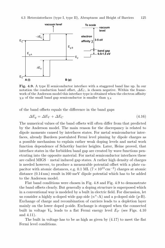
4.3 Heterointerfaces (type I, type II), Abruptness and Height of Barriers 125
Fig. 4.9. A type II semiconductor interface with a staggered band line up. In ournotation the conduction band offset, ∆EC , is chosen negative. Within the frame-work of the Anderson model this interface type is obtained when the electron affinityχB of the small band gap semiconductor is smaller than χA
of the band offsets equals the difference in the band gaps
∆Eg = ∆EV + ∆EC (4.16)
The numerical values of the band offsets will often differ from that predictedby the Anderson model. The main reason for the discrepancy is related todipole moments caused by interfaces states. For metal semiconductor inter-faces, already Bardeen postulated Fermi level pinning by dipole charges asa possible mechanism to explain rather weak doping levels and metal workfunction dependence of Schottky barrier heights. Later, Heine proved, thatinterface states in the forbidden band gap are created by wave functions pen-etrating into the opposite material. For metal semiconductor interfaces theseare called MIGS – metal induced gap states. A rather high density of chargesis needed however, to produce a measurable potential offset with a plate ca-pacitor with atomic distances, e.g. 0.1 ML (7× 1013 cm−2) charges at atomicdistance (0.14 nm) result in 160 meV dipole potential which has to be addedto the Anderson model.
Flat band conditions were chosen in Fig. 4.8 and Fig. 4.9 to demonstratethe band offsets clearly. But generally a doping structure is superposed whichin a conventional way is modeled by a built in electric field. For discussion, letus consider a highly n-doped wide gap side (n+-A) and a p-doped side (p-B).Exchange of charge and recombination of carriers leads to a depletion layermainly on the lower doped p-side. Exchange is stopped when the connectedbuilt in voltage Vbi leads to a flat Fermi energy level EF (see Figs. 4.10and 4.11).
The built in voltage has to be as high as given by (4.17) to meet the flatFermi level conditions.

126 4. Realisation of Potential Barriers
qψbi = EgA − ∆EV − ECF (A) − EFV (B)= EgB + ∆EC − ECF (A) − EFV (B) (4.17)
Certain combinations of heterostructures and dopings form a potential notchat the interface, e.g. the n+-wide band gap combined with a p-small bandgapat a type I interface (Fig. 4.10). In the given example the conduction potentialnotch collects two-dimensional electrons at the interface. For applications likethe hetero-bipolar-transistor the electrons should rapidly emit into the lowband side. Therefore, a potential as given by the type II interface is morefavourable.
Fig. 4.10. A doped heterojunction with n+-A and p-B semiconductor (type Iinterface). A flat Fermi energy is obtained with a depletion layer with ψbi voltagedrop
Fig. 4.11. A n+ −A/p−B heterostructure (with the same doping as in Fig. 4.10)with type II interface

4.3 Heterointerfaces (type I, type II), Abruptness and Height of Barriers 127
4.3.1 Modulation Doping
In order to increase the mobility of two-dimensional carriers the doping wasfurther refined. The realization of a high mobility two-dimensional electrongas has been made possible thanks to the modulation-doping technique, whichwas first applied by Dingle and Stormer to GaAs/GaAlAs heterostructures.Section 7.4.1 will review modulation doping in the Si/SiGe materials system.The idea of selective doping of heterostructures has proved to be very pow-erful. The idea is best explained by δ-doping spike distant from the interfaceby a spacer distance di (Fig. 4.12).
Fig. 4.12. Modulation doping. Demonstration of the effect of higher modulationdoping (NS2 > NS1) on the conduction band edge Ec. Cross hatched area (betweenE0 and Ef ) is proportional to the electron states in a two-dimensional carrier system
Let us first assume for simplicity that all the donors (of sheet densityNs) are ionised and the electrons (sheet density ns; ns = Ns for flat bandconditions) are collected in the potential notch at the other side of the inter-face. For complete ionisation we assume the Fermi level to be held below theconduction band neglecting high doping effects such as band gap shrinkage.We discuss qualitatively the influence of sheet doping, Ns, of spacer thick-ness, di, and of an applied gate voltage. In Fig. 4.12 the conduction bandedge of an n-modulation doped heterostructure is shown. The electric field(F = qns/ε0εr) between the positive donor ions (δ-doping with sheet densityNs1) and the electrons in the well build up an energy barrier with heightq2ns × di/ε0εr. The band offset, ∆EC , at the interface forms a well whosewidth is roughly proportional to the inverse of ns. This is because the fieldstrength (gradient of the potential) at the interface follows ns leading to anincreasing energy position E0 of the first confined electron state above thewell bottom. The Fermi energy level lies above the electron state E0 at anenergetic position also proportional to the density ns, because the density ofstates is constant in a two-dimensional carrier system.

128 4. Realisation of Potential Barriers
EF − E0 = ns/g2D (4.18)
The ground energy E0 may be approximated with reasonable accuracy bythe first confined state of a one sided triangular potential well (see Chap. 3).The 2D density of states g2D is also given in Chap. 3. The simple formulationof (4.18) is strictly valid only for Fermi statistics at 0K but it is also areasonably good approximation at room temperature. More important is tocheck the energetic position of the next higher energy levels. The partlyoccupation of the next energy level E1 has to be considered if the Fermienergy is higher than E1. Equation (4.18) reads then
(EF − E0) + (EF − E1) = ns/g2D with (EF > E1) (4.19)
Equation (4.18) (or (4.19) if EF > E1) determines the position of theFermi energy, EF , solely as a function of the channel electron sheet densityns. On the other side of the heterojunction (left side in Fig. 4.12) also twoparts contribute to the energetic difference to the Fermi energy, the electricfield barrier as given above and the energy difference EFb between conductionband in the bulk and the Fermi energy (see Fig. 4.12). The height of theelectric field barrier q2/ε0εr(nsdi) is proportional to the sheet concentrationns. Both effects lead to an upshift of the Fermi level EF with increasing NS
and they mark together with the downshift of the conduction band left side ofthe barrier the highest doping available with complete ionization (right sideof Fig. 4.12). Higher doping suffers from the incomplete transfer of electronsand parallel conduction in the δ-layer. The conduction band is above theFermi level by the amount EFb at the position of the δ-doping.
EFb = ∆EC − E0 − ns
g2D− q2
ε0εr(nsdi) (4.20)
where g2D is the constant density of states of a 2-dimensional (2D) carriersystem. This equation (4.20) is valid for complete charge transfer. For incom-plete transfer instead of NS the transferred (channel) density has to be taken.In our simplifying approximation the maximum channel density is obtainedwhen ∆EFb = 0. The structure of (4.20) is most easily seen for the case ofvarying spacer thickness where only the last term is changed. Figure 4.13demonstrates the band structure when the spacer thickness is reduced by afactor of 2. The left side shows the diagram for the maximum spacer widthdi (2) at which complete transfer is possible. By reducing the width nothingchanges on the channel side, only at the spacer side does the potential barriershrink by a factor 2.
For a given heterostructure (given ∆EC , m∗, εs) the set of equations (4.18)-(4.20) describes completely the Fermi energy, EF , and the bulk conductionband, EFb, as function of ns and di. With indirect semiconductors the properchoice of the effective mass is often the practical problem, its solution is shownin the next section when the influence of strain on the bandstructure is treated(Sect. 4.4).

4.3 Heterointerfaces (type I, type II), Abruptness and Height of Barriers 129
Fig. 4.13. Modulation doping. Demonstration of the effect of the spacer width di.Left: large spacer. Right: thin spacer
Let us consider an important special case (a strained-Si channel) thatelectrons with the longitudinal mass m∗
l are confined by the potential well(by this mass therefore the energy E0 is determined) and perpendicular wavevectors with transversal mass m∗
t contribute to the 2D density of states (g2D
is determined by m∗t ). In the next figure (Fig. 4.14) the maximum sheet
carrier density, ns,max, is calculated using the above given choice of materialconstants and using the simplifying assumption EFb = 0.
Up to now we have assumed an ideal δ−doping where the electric field, F ,stops immediately at the sheet doping. What is changing when a thin (thick-ness dd) layer with high doping density, ND, provides the carrier? The onlychange is on the left side of the heterostructure where the electric field bar-rier, ∆Eib, (fourth term in (4.20)) increases because the field now penetratesfrom the spacer into the doping by a width ns/ND.
The electric field barrier, ∆Eib, reads now
∆Ebi/q =q
ε0εrns
(di +
(ns
2ND
))(4.21)
For ND → ∞ the term converges to qε0εr
(nsdi) as used in (4.20).
4.3.2 Gated Channel
Up to now we have assumed flat band conditions at the surface with noelectric field between the δ-doping and the surface. This condition is changedby applying a proper gate voltage in a gated structure. Let us consider a gatedSchottky barrier which adjusts the electron surface potential ψs (Fig. 4.15).
Now, only a fraction α2D of the electrons are transferred to the chan-nel, the other fraction (1-α2D) is transferred to the gate electrode. On theheterostructure side again (4.18) may be used but with ns = α2DNS as theelectron density in the channel. On the gate side the relation holds
qψs + EFb = φB + (−qV ) (4.22)

130 4. Realisation of Potential Barriers
Fig. 4.14. The spacer width, di, and maximum sheet concentration, ns,max, forvarious band offsets, ∆EC . For calculation of E0 the approximation (4.26) wasused (m∗
l = 0.92m0). For calculation of g2D (3.91) was used (gs = 2, gv = 2,m∗
t = 0.19m0)
Fig. 4.15. A gated modulation doped heterojunction. An applied voltage (−V )to a metal gate (Schottky barrier φB) shifts the surface energy by an amount ψS
compared to the flat band conditions (ψS = 0)

4.3 Heterointerfaces (type I, type II), Abruptness and Height of Barriers 131
The surface potential ψs is given by the product of the electric field qε0εr
NS(1−α2D) and the cap thickness dcap.
ψs =q
ε0εrNS(1 − α2D)dcap (4.23)
For flat band conditions the surface potential ψs = 0. The voltage is the flatband voltage VFB
VFB =φB
q− ∆EC
q+
q
ε0εrNSdi +
NS
qg2D+ Const.N
2/3S (4.24)
The surface potential ψs is again somewhat larger (same reason as explainedin (4.21)) if the δ−doping is replaced by a thin (thickness dd), highly doped(doping density ND) layer.
ψs =q
ε0εrNS(1 − α2D)
(dcap +
12
NS(1 − α2D)ND
)(4.25)
Exact solutions of equations 4.18- 4.25 need a self consistent solution of theenergy level E0 as function of NSα2D. For a rough assessment a trial func-tion in a variational solution may be used leading to the following carrierdependence for the triangular potential.
E0
q∼= 2
(h2q
m∗ε20ε
2r
)1/3
(NSα2D)2/3 (4.26)
Const. = 2(
h2q
m∗ε20ε
2r
)1/3
The following implicit equation for the fraction α2D is obtained.
∆EC
q− φB
q+ V + NS
q
ε0εrdcap = (4.27)
(NSα2D)[
q
ε0εr(dcap + di) +
1qg2D
]+ Const. (NSα2D)2/3
It should be remembered this equation is valid as long as EFb is larger thanzero, which can be tested with (4.18), and the channel density ns is given byNSα2D.
With increasing reverse voltage (Vr < 0V) the transferred fraction α2D
decreases and reaches 0 at the threshold voltage VT .
VT =φB
q− ∆EC
q− q
ε0εrNSdcap (4.28)
That means that the threshold voltage, VT , is determined by the materialsystem properties φB , ∆EC and the technological properties NS , dcap. Ahigher sheet doping NS or a larger cap layer, dcap, shifts the threshold voltageto more negative voltages (for a n-channel device).

132 4. Realisation of Potential Barriers
For an overview of all the effects let us change the voltage V between thegate and the channel from negative values to positive values. The semicon-ductor side is considered as a reference. The δ-doping density, NS , is chosensomewhat lower than the maximum sheet density, ns,max.
For strong negative values of the voltage V the doping layer and thechannel are depleted. At the threshold voltage VT the first electrons jumpinto the channel (Fig. 4.16, above) when the down moving first quantumwell level E0 meets the Fermi energy. In the given example of Fig. 4.16 theSchottky barrier is 0.45 eV and the threshold voltage VT is -0.15V. Withhigher Schottky barrier heights (eg. 0.7 eV) the threshold voltage would shiftto positive values with the same geometrical factors (di, dcap, NS). Withmore positive values of voltage V (V − VT > 0 V) the channel will be filledwith electrons (density ns) when the energy level E0 shifts below the Fermienergy. Do not forget that the energy E0 by itself is a function of ns, becauseof the triangular bottom of the quantum well. In Fig. 4.16 (middle) half ofthe electrons in the δ-doping jump into the channel (ns = NS/2) when thevoltage, V , reaches 0.125V. With increasing voltage VFB (flat band voltage)all the electrons from the δ-doping jump into the channel with a vanishingelectric field in the cap layer. In the example (Fig. 4.16, below) the flatband voltage VFB amounts to roughly 0.42V. Further increase of the voltagebeyond the Schottky barrier value, ΦB/q, creates a surface channel like aMOS varactor which creates high leakage currents to the non insulating gate.
The simple picture which has been presented is in reality complicated byseveral effects, the most important of which we will discuss qualitatively. Onehas to consider the finite temperature, T , the real doping is spread out bya distance dd with doping level Nd (Nd × dd = NS), and the bulk volumeis doped oppositely, that results for the treated case of an n-channel, thebulk must be p-doped to insulate the channel through p/n-junction isolation.The most prominent effect of the temperature is the finite occupation ofenergy levels even if the Fermi energy is below that energy level. This leadsto incomplete vanishing charge in the channel at strong negative voltages (subthreshold) and to incomplete vanishing electrons at the δ-doping even if thedensity is below the maximum. An exact calculation of the occupation needsconsideration of the asymmetric triangular well at the δ-doping (see Fig. 4.16,not to be confused with the one sided triangular well at the channel).
The finite thickness of the doping layer is easily calculated using Poisson’sequation. For a uniform doping Nd, with thickness dd in between the undopedspacer di and the undoped cap dcap, the voltage barriers to the spacer and
the cap read(
qε0εr
)ns
(di + ns
2ND
)and
(q
ε0εr
)(NS − ns)
(dcap + NS−ns
2ND
),
respectively. For increasing doping values ND we approximate the δ-dopingcase.
The opposite bulk doping isolates the channel from the substrate, butthat means, that a part of the electrons from the δ-doping are used to createthe depletion layer to the p-bulk. The number (NS × α′) used is given by

4.3 Heterointerfaces (type I, type II), Abruptness and Height of Barriers 133
-qV
TV
T
Fig. 4.16. A schematic diagram of the potential energy in a modulation dopedquantum well. Shown is the variation with increasing gate voltage, V , from theempty channel (threshold voltage VT ) to the full channel (flat band voltage VF B).The energy E0 is not constant but a function of the channel charge, because oftriangular well bottom

134 4. Realisation of Potential Barriers
NSα′ = NA × db
[(1 + 2
ε0εr
q
Vbi
NAd2b
)1/2
− 1
](4.29)
whereas NA and db are bulk doping density and distance of bulk doping fromδ-doping, respectively. A typical value of (NSα′) is 4 × 1011 cm−2 for NA =1017 cm−3, db = 100nm and built in voltage Vbi = 0.8V. A conceptually goodsolution to this problem is delivered by a second δ-doping below the quantumwell.
4.4 Influence of Strain on Bandstructure
Application of strain is frequently used for the investigation of basic materialproperties, from such studies we understand the effects of hydrostatic pressureand uniaxial stress.
Strain has two main effects on the band structure: hydrostatic strainshifts the energetic position of a band and uniaxial strain splits degeneratebands (Fig. 4.17). The strain state of the semiconductor can be expressed by
Fig. 4.17. A schematic diagram representation of the strain on a triply degenerateband. Hydrostatic strain shifts the absolute energy position of the band. Uniaxialstrain splits the degeneracy; illustrated is a case where the threefold degenerateband is split into a set of twofold degenerate bands at lower energy plus a singlydegenerate band at higher energy. Note that the average over the three bands(dotted line) is unaffected by uniaxial strain
the strain tensor ε. The hydrostatic strain, corresponding to the fractionalvolume change ∆V
V , is given by the trace of the strain tensor, which amountsfor biaxial strained epitaxial layers to
∆V
V= Tr(ε) = 2ε + εz, (4.30)
where the normal strain εz in an isotropic notation given by (2.24b).For simplicity we assume the z-direction in [001], a threefold degenerate
valence band at k = 0 (light holes 1, heavy holes 2, spin-orbit split-off holes3) and an indirect conduction band with sixfold degenerate ∆ valleys (in the(100) directions).
The effect of hydrostatic and biaxial strains on the bandstructures is ex-pressed via deformation potentials. These deformation potentials have been

4.4 Influence of Strain on Bandstructure 135
determined experimentally and theoretically for Si and Ge; no direct deter-minations have been performed for SiGe alloys. Linear interpolation tends,however, to be a good approximation. The deformation potentials for hydro-static strains will be denoted by the symbol a, and the deformation potentialfor uniaxial strain in tetragonally distorted cubic lattice cells are denoted byb.
4.4.1 Hydrostatic Strain
Hydrostatic strain shifts the average position of the valence and the conduc-tion band by ∆Ev,av and ∆Ec,av, respectively.
∆Ev,av = av(2ε + εz) = 2ε1 − 2ν
1 − νav (4.31a)
∆Ec,av = ac(2ε + εz) = 2ε1 − 2ν
1 − νac (4.31b)
where ν is Poisson’s ratio. Numerical values of the hydrostatic deformationpotentials av and ac are given in Table 4.2. The selected values follow valuesrecommended by C. Van de Walle, who performed the basic studies on bandoffsets in the strained SiGe system.
Table 4.2. The deformation potentials av and ac for hydrostatic strain in Si andGe. The deformation potentials bv and bc are already given in a notation appropriatefor tetragonal strain (E1, E2 in Kane’s notation, and Ξd + 1
3Ξu, Ξu in Van de Walle
notation).
Material Deformation potential (eV)
av ac bv bc
Si 2.46 4.18 -2.35 9.16
Ge 1.24 2.55 -2.55 9.42
4.4.2 Uniaxial Strain
The biaxial strain in the epitaxial plane can be considered as hydrostaticdeformation superposed by an uniaxial strain (εz − ε) perpendicular to theplane. This uniaxial strain component is written in isotropic notation as
εz − ε = −ε1 + ν
1 − ν, (4.32)
In the valence band the light hole (lh) band is shifted by 3bv(εz−ε) comparedto the heavy hole and spin-orbit split-off band. Compared to the average theshifts are given by

136 4. Realisation of Potential Barriers
∆Ev1(lh) = 2bv(εz − ε) = −2bvε1 + ν
1 − ν(4.33a)
∆Ev2 = ∆Ev3 = −bv(εz − ε) = bvε1 + ν
1 − ν(4.33b)
In the absence of strain the threefold degeneracy of the valence band is alreadylifted by the spin orbit interaction and splits the bands by an amount of ∆0.With respect to the average band position Ev,av two bands are shifted upby an amount of ∆0
3 (the light and heavy hole bands, which are denotedEv1, Ev2), while one band is shifted down by an amount 2∆0
3 (the spin-orbitsplit-off band, which we denote Ev3).
For completeness the relations are given for lifting of the valence banddegeneracy by strain and band orbit interaction. The superposition of botheffects is nonlinear for the light hole and spin orbit split-off band.
∆Ev1 = −16∆0 +
b
2(εz − ε) +
12
√∆2
0 + 2∆0b(εz − ε) + 9b2(εz − ε)2 (4.34a)
∆Ev2 =13∆0 − b(εz − ε) (4.34b)
∆Ev3 = −16∆0 +
b
2(εz − ε) −
12
√∆2
0 + 2∆0b(εz − ε) + 9b2(εz − ε)2 (4.34c)
The strain lifts the sixfold (6g) degeneracy of the conduction band into thefourfold (4g) degenerate bands with energy minima lying in-plane and thetwofold degenerate band with energy minima lying perpendicular to the (001)plane. For (001) growth and ∆ type energy minima the energy shifts ∆Ec
with respect to the average are easily written as
∆Ec(2g) =23bc(εz − ε) = −2
3bcε
1 + ν
1 − ν(4.35a)
∆Ec(4g) = −13bc(εz − ε) =
13bcε
1 + ν
1 − ν(4.35b)
Let us now consider a model material with simple properties av = 2eV,ac = 3 eV, bv = -2.5 eV, bc = 9 eV, ∆0 = 0, ν = 1
3 under either tensileor compressive biaxial strain ε of magnitude 0.01. First we investigate thevalence band under the influence of strain (Fig. 4.18). The band average Ev,av
is shifted up by tensile strain (+20meV) and shifted down by compressivestrain. Tensile strain further shifts up the light hole (lh) energy levels by100meV while heavy holes (hh) are lowered by 50meV. In our model materialthe spin-orbit split-off holes (soh) are degenerate (∆0 = 0) with heavy holesat k = 0. As a result of tensile strain the light holes energy (Ev1) are liftedby 120meV, while the heavy holes (Ev2 = Ev3) are lowered by 30meV.
Under compressive biaxial strain (growth on a substrate with a smallerlattice constant) the heavy hole band will be at the band edge; under tensile

4.4 Influence of Strain on Bandstructure 137
Fig. 4.18. The valence band splitting under the influence of strain for | ε |= 0.01.For the properties of the model material see the text
strain (growth on a substrate with a larger lattice constant) the light holeband will be preferentially occupied. The different effective masses of the lightand heavy hole bands lead to different behaviour in terms of the mobility ofcarriers or confinement shifts in the quantum wells. One can therefore usestrain to tailor the band structure according to the needs of a particularapplication.
Now, we investigate the Si-like conduction band (indirect, ∆-minimum)under the influence of tensile strain (ε = 0.01). The average energy,Ec,av, isshifted up by 30meV. The twofold (2g) electrons perpendicular to the planeare shifted down by ∆Ec(2g) = 120meV, the fourfold (4g) in-plane electronsare shifted up by ∆Ec(4g) = 60meV (Fig. 4.19) resulting in a final energyposition of Ec(2g) = -90meV, Ec(4g) = +90meV with 180meV splitting.The dominant effect of band splitting compared to the shift of the averageenergy results in the band gap being reduced by the strain. With tensilestrain the smallest gap is between the light hole valence band and the twofold(2g) electrons with a band gap shrinkage of 210meV (120meV and 90meVcontribution from valence band and conduction band, respectively). Withcompressive strain the lowest gap is between hh states in the valence band and4g electron states in the conduction band. The band gap shrinkage amountsto 120meV (30meV and 90meV from the valence band and conduction band,respectively).

138 4. Realisation of Potential Barriers
Fig. 4.19. The conduction band splitting under the influence of strain for | ε |=0.01. The same model material has been used as in Fig. 4.18
4.5 Band Alignment of Strained SiGe
When two semiconductor are joined at a heterojunction, discontinuities occurin the valence band and in the conduction band. In the absence of strain, i.e.for a lattice matched interface, the alignment simply requires one to determinehow the band structures of the two materials line up at the interface; the lineup then produces values for the valence band discontinuity, ∆Ev, and theconduction band discontinuity, ∆Ec. When the materials are strained, thestrains will produce additional shifts (due to hydrostatic strain) and splittings(due to biaxial strain) as described in the forgoing section.
We will follow here the treatment of Van de Walle who first consideredthe average energy, E0
v , of the unstrained valence band and then added theinfluence of strain to obtain the individual energy levels.
4.5.1 Average Valence Band Energy E0v
The average valence band energy of Ge is roughly 0.58 eV above that valueof Si (Note: Both, the experimental and theoretical values on that propertyare uncertain by about 0.1 eV). That would result in a valence band offsetbetween unstrained Si and unstrained Ge of 0.662 eV, because the highestvalence bands (lh, hh) are shifted up by ∆0/3. The spin orbit splitting ∆0

4.5 Band Alignment of Strained SiGe 139
increases strongly from Si (∆0 = 44meV) to Ge (∆0 = 290meV). For bothquantities E0
v and ∆0 we will assume a linear relationship with the chemicalcomposition of an Si1−xGex alloy (expressed by atomic Ge content x).
E0v,av(SiGe) = 580 meV × x − 44
3meV (4.36)
∆0(SiGe) = 44 meV + x × 246 meV (4.37)
The valence band edge (lh, hh) of unstrained Si is taken as reference energy.The valence band edge Ev,1 = Ev,2 of unstrained SiGe is then given by
SiGe : E0v,av + ∆0/3 = 662 meV × x (4.38)
(Remember; the notation v1, v2, v3 is used for the light hole, heavy hole andspin-orbit split-off subbands of the valence band). The energetic position ofthe conduction band is more complicated, because of band bowing with Gecontent x and because of Ge-like (eightfold, 8g) band minima for high Gecontents (x > 0.85). We consider here only the mainly dominating Si-like(6g, unstrained SiGe) states. The reader is referred to the section on FurtherReading, e.g. D. Paul, for the small regime around Ge with Ge-like states.
The band gap E0g of unstrained SiGe is roughly given by a parabolic law
E0g = (1.17 − 0.44x + 0.206x2) eV (4.39)
which is obtained by adding the binding energy of the free exciton (14.7meVfor Si, 4.15meV for Ge) to the excitonic bandgap obtained from low temper-ature photoluminescence measurements (Weber, Alonso).
4.5.2 Compressive Strain
A typical situation for compressive strain is given by a pseudomorphic SiGefilm on a Si substrat.
We consider only the energy offsets for the most occupied subbands (high-est valence band, lowest conduction band). For compressive strain these arethe heavy hole valence band (Ev2) and the (4g) in plane conduction band min-ima (Ec4). The typical contributions for the valence band offset are shown inFig. 4.20 on the example of strained Ge on an unstrained Si substrate. TheSi substrate is on the left side with the average valence band energy Ev,av
an amount ∆0/3 = 44/3meV (∼= 15meV) below the valence band edge Ev
(≡ Ev1 = Ev2). On the Ge side the hypothetical unstrained average E0v,av is
0.58 eV above the average Si level (chemical composition shift). The hydro-static strain (compressive strain has negative sign) shifts down the averagelevel to Ev,av. The uniaxial component splits the valence bands with theEv2 energy (heavy hole states) as the upper level for compressive strain. Theconduction band offset may be constructed in the same way by adding theband gap to the average valence band energy and then applying the strain.With compressive strain the fourfold degenerate (4g) in plane conduction

140 4. Realisation of Potential Barriers
Fig. 4.20. The theoretical valence-band lineups at an interface between unstrainedSi and strained Ge (not to scale)
band minima Ec4 are lowest in energy. Figure 4.21 shows the valence bandoffsets ∆Ev(v2) and the conduction band offset ∆Ec(4g) as function of theGe content for strained SiGe on Si. For comparison the offsets for the othersubbands which do not define the band edge are also shown. The valenceband discontinuity ∆Ev increases rather linearly to the strained Ge value of0.78 eV, while the conduction band discontinuity is clearly nonlinear, becauseof the band gap bowing and it is quite small (Note: the band offset ∆Ec inFig. 4.21 is shifted by 1.17 eV to separate it from ∆Ev).
Fig. 4.21. The band offsets ∆Ev, ∆Ec for a pseudomorphic Si/Si1−xGex hetero-junction as a function of alloy composition x in the overlayer. ∆Ev is defined bythe heavy hole (v2) level, ∆Ec by the in plane (4g) level. For better readability theconduction band offset ∆Ec is shifted up by the bandgap difference of Si (1.17 eV)

4.5 Band Alignment of Strained SiGe 141
4.5.3 Tensile Strain
A typical situation for tensile strain would be a strained-Si channel on arelaxed SiGe buffer (methods to obtain strain adjustment will be discussedin Chap. 2).
Here the light hole (v1) states mark the valence band edge while theperpendicular (2g) states mark the conduction band edge. The treatment issimilar to the compressive strain treatment, but one has to consider, that theenergy splitting of the light hole (v1) states is more complicated than that ofthe heavy holes (v2), because of interference with spin orbit interaction (seeforgoing section).
The results of the calculation for a strained-Si quantum well on a relaxedSi1−yGey substrate heterojunction are given in Fig. 4.22. The larger band gapoverlayer of Si is lower in the valence band edge (v1) which is as expected butis also lower in the conduction band edge (2g) energy which is a characteristicsof a type II heterostructure.
Fig. 4.22. The band offsets ∆Ev, ∆Ec for a pseudomorphic relaxed-Si1−yGey/strained-Si heterojunction as a function of alloy composition y of thesubstrate. The valence band offset ∆Ev is defined by the v1 (light hole) state, theconduction band offset ∆Ec is defined by the 2g (perpendicular to the interfaceplane) states. ∆Ec is shifted up by 1.17 eV as in Fig. 4.21

142 4. Realisation of Potential Barriers
4.6 Further Reading
1. D.J. Paul, Semiconductor Science and Technology 19, R59 (2004)2. M.J. Kelly, Low Dimensional Semiconductors: Materials, Physics, Tech-
nology, Devices” OUP, Oxford (1995)3. J.H. Davies, The Physics of Low Dimensional Semiconductors, CUP,
Cambridge (1998)4. C.K. Maiti, N.B. Chakrabarti, S.K. Ray, Strained Silicon Heterostruc-
tures Materials and Devices, The Institution of Electrical Engineers, Lon-don (2001)

5. Electronic Device Principles
This chapter will review the major types of devices which have been demon-strated or suggested as possible devices in the Si/SiGe heterostructure sys-tem. At present MOSFETs dominate the semiconductor markets mainly inthe circuit form of CMOS but the first transistor action was produced ina germanium bipolar device in 1947. The first SiGe transistor to be on themarket place is the heterojunction bipolar transistor (HBT) which will be re-viewed in Chap. 6. This chapter will therefore start on bipolar devices beforemoving to field effect transistors (FETs) such as MOSFETs.
5.1 The p-n Junction
The basic building block and foundation of many electronic devices is thep-n junction or diode. The physics of such junctions was originally developedby Shockley in 1950. The physics is still central in the design of present dayULSI MOSFETs and bipolar transistors.
Let us consider the case of an abrupt junction where the doping in thesemiconductor changes from NA to ND over a few atomic layers. Figure 5.1shows the typical structure along with the space charge distribution and theresulting band structure.
The first case to consider is for zero applied potential and no current flow.The current density is given by
Jn = qµnnF + qDn∂n
∂x= qµn
(nF +
kBT
q
∂n
∂x
)= 0 (5.1)
for electrons where the electric field is F , the electron mobility is µn, q is theelectronic charge of an electron, Dn is the electron diffusion constant and nis the electron concentration. Similarly for holes
Jp = qµppF − qDp∂p
∂x= qµp
(pF − kBT
q
∂p
∂x
)= 0 (5.2)
To solve these equations, (3.167) from Chap. 3 needs to be substituted into(5.1) and (5.2) which gives the result

144 5. Electronic Device Principles
∂EF
∂x= 0 (5.3)
electrons
holes
Fig. 5.1. (a) A schematic diagram of an abrupt p-n junction. (b) The band diagramof the p-n junction. (c) The space-charge distribution in the junction at thermalequilibrium
Therefore the requirement of zero current flow in the systems forces theFermi energy to be constant across the junction. Electrons and holes willtherefore redistribute close to the interface forming depletion regions as shownin Fig. 5.1 (c). The built-in potential created by this redistribution is givenby
qψbi = Eg − (qψn + qψp) (5.4)
= kBT ln(
NcNv
n2i
)−[kBT ln
(Nc
nn
)+ kBT ln
(Nv
pp
)]
∼= kBT ln(
NDNA
n2i
)(5.5)

5.1 The p-n Junction 145
where np is the electron density in the p-semiconductor and pp is the holeconcentration in the p-semiconductor. At equilibrium
nnpn = nppp = n2i (5.6)
therefore
ψbi =kBT
qln(
pp
pn
)=
kBT
qln(
nn
np
)(5.7)
One can turn (5.7) around to find the relationship between the electronand hole densities on either side of the junction which are
pn = pp exp(− qψbi
kBT
)(5.8)
np = nn exp(− qψbi
kBT
)(5.9)
Since no current flows, the electric field in the neutral regions well awayfrom the junction must be zero. Therefore the negative charge per unit areain the p-side must equal the positive charge per unit area in the n-side andso
NAxp = NDxn (5.10)
Next we need to apply Poisson’s equation to the abrupt junction relatingthe electrostatic potential, ψ to the charge density, ρ through
∂2ψ
∂x2= −∂F
∂x= −ρ (x)
εoεr= − ρ
εoεr
[p (x) − n (x) + N+
D (x) − N−A (x)
](5.11)
and so with approximations in the regime 0 < x ≤ xn gives
∂2ψ
∂x2∼= − q
εoεrND (5.12)
while in the regime −xp ≤ x < 0 the result becomes
∂2ψ
∂x2∼= q
εoεrNA (5.13)
By integrating (5.12) and (5.13), the appropriate electrics fields can befound as
F (x) = −qNA (x + xp)ε0εr
(5.14)
for the region −xp ≤ x < 0 and

146 5. Electronic Device Principles
F (x) =qND (x − xn)
ε0εr(5.15)
for the region 0 < x ≤ xn.The maximum electric field occurs at x = 0 and is given by
|Fm| =qNDxn
ε0εr=
qNAxp
ε0εr(5.16)
Integrating either of (5.14) or (5.15) produces the potential distribution
ψ (x) = Fm
(x − x2
2WD
)(5.17)
where WD is the depletion width which may be defined as
ψbi =12FmWD =
12Fm (xn + xp) (5.18)
WD may be given explicitly by eliminating Fm from (5.16) and (5.18) whichgives for an abrupt two sided junction
WD =
√2ε0εr
q
(NA + ND
NAND
)ψbi (5.19)
If the junction is much more heavily doped on one side, i.e. NA ND orvice versa then
WD =
√2ε0εrψbi
qND√
2ε0εrkBT
q2NDln[NDNA
n2i
](5.20)
The depletion width decreases as the doping density in the semiconduc-tor increases (Fig. 5.2). This becomes extremely important when designingadvanced bipolar or FET transistors where the typical dimensions will becomparable to depletion widths. The doping concentration must thereforebe increased as sizes are scaled down to reduce the depletion widths andtherefore the active size of the transistor.
5.1.1 The Current Voltage Characteristics of a p-n Junction
In calculating the current voltage characteristics of a p-n junction, as voltagesare applied across the junction, the chemical potentials and Fermi energiesare different in different parts of the device. It is easier to define quasi-Fermipotentials and use these in place of the intrinsic potential. Therefore, rewrit-ing the current density from (5.1) and (5.2)
Jn = −qnµndφn
dx(5.21)

5.1 The p-n Junction 147
Fig. 5.2. The built in potential ψbi and the depletion width WD for abrupt p-njunctions in both Si (line) and Ge (dotted line) where one side is heavily doped.The depletion width corresponds to the lightly doped side
Jp = −qpµpdφp
dx(5.22)
where the quasi-Fermi energies for electrons and holes are defined as
EFn = Ei + kBT ln(
n
ni
)(5.23)
EFp = Ei − kBT ln(
p
ni
)(5.24)
where ψi is the intrinsic potential defined in terms of the intrinsic Fermi level,Ei as
ψi = −Ei
q(5.25)
The pn product may be derived in terms of the quasi-Fermi energies as
pn = n2i exp
[EFn − EFp
kBT
](5.26)
The spacial variation of the quasi-Fermi energies in a p-n junction areillustrated in Fig. 5.3. Far from the junction, n = n0 and p = p0 and soEFn = EFp = EF . As is shown in Fig. 5.3, the applied voltage across thediode, V is

148 5. Electronic Device Principles
Fig. 5.3. The quasi-Fermi energies EFn and EFp in a p-n diode for (a) forwardbias (V > 0) and for reverse bias (V < 0)
qV = EFn − EFp for −xp ≤ x ≤ xn (5.27)
The diode is described as being forward biased when a positive voltage isapplied to the n-region if the p-region is earthed and the diode is reversebiased if a negative voltage is applied. Figure 5.3 shows how the bands changewith the two applied biases. Using (5.26) and (5.27), the electron density atthe depletion layer edge on the p-side (at x = −xp) is given by
np (−xp) =n2
i
pp (−xp)exp
[qV
kBT
](5.28)
=np0 (−xp) pp0 (−xp)
pp (−xp)exp
[qV
kBT
](5.29)
≈ np0 (−xp) exp[
qV
kBT
](5.30)
The approximation in the last line is that the majority carrier densityis large compared to the minority carrier density and therefore the majoritycarrier density is equal to its equilibrium value. Using similar arguements,the hole concentration at x = xn can be shown to be

5.1 The p-n Junction 149
pn (xn) ≈ pp0 (xn) exp[
qV
kBT
](5.31)
The continuity equation for electrons is
∂n
∂t=
1q
∂Jn
∂x− Rn + Gn (5.32)
=1q
∂Jn
∂x− n − n0
τn(5.33)
where Rn is the electron recombination rate, Gn is the electron generationrate (see Sect. 3.7.2) and τn is the electron lifetime defined as
τn =n − n0
Rn − Gn(5.34)
and n0 is the electron concentration at thermal equilibrium.Let us now consider the electrons in a uniform p-region of the p-n diode
where the electric field is zero so that F = 0 and ∂F/dx = 0. Substituting (5.1)into (5.33) and solving for the diode in the steady state gives
∂np
∂t= Dn
∂2np
∂x2− np − np0
τn= 0 (5.35)
This equation is typically rewritten using the electron diffusion length definedas
Ln =√
τnDn (5.36)
and then solved using the boundary conditions of (5.30) and np (x = ∞) =np0 to give
np − np0 = np0
(exp
[qV
kBT
]− 1
)exp
[− (xp + x)Ln
](5.37)
and the electron current density is
Jn =qDnnp0
Ln
(exp
[qV
kBT
]− 1
)(5.38)
Similarly, the n-type side of the device has
Jp =qDppn0
Lp
(exp
[qV
kBT
]− 1
)(5.39)
The total current is given by the sum of (5.38) and (5.39) which is
J =(
qDnnp0
Ln+
qDppn0
Lp
)(exp
[qV
kBT
]− 1
)(5.40)
This is the famous Shockley equation for an ideal p-n junction and is plottedin Fig. 5.4

150 5. Electronic Device Principles
-2
2
4
6
8
10
12
14
-5 -4 -3 -2 -1 1 2 3 4 5
qVkBT
J / Js
Fig. 5.4. The ideal current voltage characteristics of a p-n junction. Js is theprefactor in (5.40)
5.2 The Silicon Bipolar Transistor
The silicon bipolar device is still heavily used in many applications such asanalogue and high speed digital electronics. While it typically runs muchfaster than equivalent design-rule MOSFETs, it consumes more power thanMOSFETs and therefore its integration density is smaller. The basic physicsrelies heavily on the p-n junction (Sect. 5.1) as the transistor consists oftwo back-to-back p-n junctions. While both p-n-p and n-p-n varieties canbe designed and fabricated, we will concentrate on the n-p-n device as thisis the easiest to modify into a heterojunction bipolar process which will bediscussed in Sect. (6.4). Most semiconductor text books provide an overviewof the operation of the bipolar transistor but the reference by Taur and Ningin Sect. 5.4 is recommended as it covers in most detail the latest advancedbipolar designs used in present day ULSI.
In the following section for equations, the subscripts, E,C and B will beused for the emitter, collector and base regions of the transistor respectively.The subscripts n and p will correspond to the semiconductor type so that nn
will correspond to the majority electron concentration in an n-doped regionwhile np will correspond to the minority electron concentration in a p-dopedregion.
If Kirchoff’s circuit laws are applied to a bipolar transistor then thereare only two independent voltages and two independent currents (Fig. 5.5).There are a number of different ways a bipolar transistor can be configured

5.2 The Silicon Bipolar Transistor 151
Fig. 5.5. The schematic diagram of different bipolar transistor configurations
in a circuit as an amplifier. These are the common base (Fig. 5.5(a)), com-mon emitter (Fig. 5.5(b)) and the common collector (Fig. 5.5(c)). The mostfrequently used configuration is the common emitter that can be used forcurrent, voltage or power amplification.
∆Vn
EgE
EgB
∆Vp
emitter base collector
Ec
Ev
Fig. 5.6. The schematic energy band diagram of a bipolar transistor
Figure 5.6 shows a schematic diagram of the typical n-p-n structure alongwith the band structure and important parameters for operation. Bipolartransistors are normally vertical devices with the base and collector being

152 5. Electronic Device Principles
formed by ion implantation. The typical poly-Si emitter bipolar transistorstructure used in present advanced Si bipolar designs is shown schematicallyin Fig. 5.7. Lateral version do exist but the control of the base width thendepends on the lithographic resolution which to date is larger than verti-cal dimensions created by implantation. The vertical device is the dominantversion and is used particularly for high speed applications while the lateraldevice is mainly used in specific BiCMOS circuit applications where speed isnot the most important parameter. We will concentrate on the vertical bipo-lar devices in the rest of this chapter but the equations can also be appliedto lateral devices.
p+ poly-Si p+ poly
n+ poly-Siemitter
p basep+ p+
n collectorn+
SiO2
SiO2SiO2
metal metal
SiO2 SiO2
n+ subcollector
p-substrate
polySi
polySi
SiO2
poly-Si filleddeep trench isolation
SiO2
Fig. 5.7. The schematic diagram of a poly-Si emitter bipolar transistor which istypically used in production
The bipolar has a number of natural advantages:
1. Being a vertical transistor, the control of the important dimensions whichdetermine the transit time of electrons through the transistor and hencethe speed can be tailored to be much smaller than present lithographi-cally defined lateral dimensions. Most bipolars use implantation for theformation of the base but epitaxy may also be used to form narrowerbase widths.
2. The entire area of the device conducts current unlike a FET where only asmall 2D region conducts. Therefore large output currents per unit areacan be maintained.
3. The output current is directly controlled by the input voltage through therelation Ic = exp
(qV
γkBT
)with γ ≈ 1. The transconductance is therefore
gm = qIc/kBT which is the highest obtainable in any three terminaldevice where the carrier density is modulated by the voltage (almostall conventional devices). The high transconductance produces low input

5.2 The Silicon Bipolar Transistor 153
1015
1016
1017
1018
1019
1020
1021
0 0.2 0.4 0.6 0.8 1
Depth from Surface (µm)
Dop
ing
Con
cent
rati
on (
cm-3
)
p
n+
n-
n+
Fig. 5.8. The schematic diagram of the typical doping used in a silicon bipolartransistor
voltage swings which is essential for low power-delay products in logicapplications.
4. The turn-on voltage of bipolar transistors, VBE , is relatively independentof device size and also process variations since it is directly related to thebuilt-in potential of a p-n junction, ψbi. This reduces variations in VBE
across a wafer as required for manufacture especially of logic circuits withsmall voltage swings.
5. The input capacitance of the bipolar transistor scales with the operatingcurrent so that the input capacitance adjusts to appropriate values athigh or low current operation. Therefore device sizes do not need to bevaried to match the driven load in many circuit designs.
Figure 5.8 shows a schematical diagram of the doping concentration nor-mally found in a modern silicon bipolar transistor. The device is quite com-plicated and is designed with a self-aligned poly-silicon emitter to reduceparasitic capacitances in the system, thereby improving high speed perfor-mance.
It will become useful later if general expressions for the bipolar transistoroperation are derived here. To start with, the current density equations whichalso include the drift effects of an electric field, F in addition to diffusioncomponents as also used in the p-n junction ((5.1) and (5.2) are the startingpoint).
Jn (z) = qnµnF + qDndn
dz(5.41)

154 5. Electronic Device Principles
and
Jp (z) = qpµpF − qDpdp
dz(5.42)
The electric field must be derived for the p-type base of the transistor.The same technique as that used for the p-n diode will be used so that thequasi-Fermi level in a p-type bulk semiconductor is given by
EFp = Ei − kBT ln[pp
ni
](5.43)
using the definition of ψi in terms of the intrinsic Fermi energy of (5.25). Theelectric field is the negative gradient of the intrinsic potential and hence
qF =dEi
dz(5.44)
F =kBT
qpp
dpp
dz+
Jp
qppµp(5.45)
Quasi-neutrality is required in the p-type base when the junction is for-ward biased since an electron current is flowing in the system and hence
pp (z) = NA (x) + np (z) (5.46)
Taking the first derivative
dpp
dx=
dNA
dx+
dnp
dz(5.47)
the built-in electrical field in the base can be found by setting np = 0 andpp = NA in (5.45) and realising that in a p-region that Jp is small so thesecond term of (5.45) is much smaller than the first term. The field is thereforegiven for vanishing injection as
F0 =kBT
qNA
dNA
dz(5.48)
The electron current in a nonuniformly doped p-type base region can befound by using (5.45) with low Jp, (5.41), (5.47) and (5.48) to give
Jn (z) = qnµnF0NA
np + NA+ qDn
(2np + NA
np + NA
)dnp
dz(5.49)
The current density in the base as injected from the emitter can be foundfor low values of current where np NA from (5.49) gives
Jn (z) ≈ qnµnF0 + qDndnp
dz(5.50)

5.2 The Silicon Bipolar Transistor 155
It is clear that this represents a drift component from the built-in electricfield due to non-uniform doping in the base and a diffusion component whichis due to the gradient in the electron concentration. If a large number ofelectrons is being injected from the emitter into the base then np NA
must be inserted into (5.49) which gives
Jn (z) ≈ 2qDndnp
dz(5.51)
Therefore the built-in electric field is negligible compared to the gradient ofthe electron concentration which dominates in this regime.
The electron current density for those injected from the emitter into thebase can also be calculated in terms of the carrier concentration in the base.We again take the current density as a function of the quasi-Fermi potentialsas defined in (5.21)
Jn = npµndEFn
dz(5.52)
The effective ionisation energy for impurities in a heavily doped semi-conductor decreases as the doping increases which results in the effectivebandgap decrease. Therefore as the band gap changes and therefore the den-sity of states changes as the doping increases, the intrinsic carrier density inthe base will also change. The standard method of incorporating this is todefine an effective intrinsic carrier density, nie and define it such that all theeffects of heavy doping are incorporated into the effective bandgap narrowing,∆Eg such that
n2ie = n2
i exp[∆Eg
kBT
](5.53)
While there are many reported experimental results of bandgap narrow-ing, the scatter in the data is large and empirical expressions are typicallyused. For ND 7×10²³ m−3, del Alamo has suggested the following empiricalrelation
∆Eg (ND) = 18.7 ln(
ND
7 × 10²³
)meV (5.54)
where ND is in units of m−3 and zero for lower doping concentrations.We have already shown for the p-n junction that the quasi-Fermi energy
for holes is approximately constant for a p-type region and therefore thegradient is zero in the base i.e.
dEFp
dz≈ 0 (5.55)
Combining (5.52) and (5.55) before substituting for EFn−EFp from (5.23)and (5.24) gives the electron current density in the base as a function ofelectron and hole concentrations as

156 5. Electronic Device Principles
Jn (z) = qDnn2
ie
pp
ddz
(nppp
n2ie
)(5.56)
In a similar fashion, the hole current density in the emitter can be derived as
Jp (z) = qDpn2
ie
nn
ddz
(nnpn
n2ie
)(5.57)
Since there is very little recombination in the thin base layer of a transis-tor, the collector current in the system is mainly due to the electrons beinginjected from the emitter into the base region of the transistor where they areswept into the collector. Referring to Fig. 5.6, the start of the quasi-neutralbase is denoted by z = 0 and the end by WB (i.e. the base width). If there isnegligible recombination in the base then Jn is independent of z and (5.56)can be integrated.
Jn
q
∫ WB
0
pp
Dnn2ie
dz =[nppp
n2ie
|z=WB − nppp
n2ie
|z=0
](5.58)
At z = 0 the electron concentration is given by (5.30)
np (0) = np0 exp[qVBE
kBT
](5.59)
with VBE the emitter-base, forward-biased voltage. At z = WB, np (WB) isnegligible compared to np (0) and so the term evaluated at WB in (5.58) canbe ignored producing
Jn
q
∫ WB
0
pp
Dnn2ie
dz =[np0 (0) pp (0)
n2ie (0)
exp(
qVBE
kBT
)](5.60)
In modern bipolar designs, the base doping concentration peaks at theemitter-base junction. Providing this peak concentration is much larger thanthe minority carrier concentration, the hole concentration is approximatelythe thermal equilibrium value of pp (0) ≈ pp0 (0) and so using np0 (0) pp0 (0) =n2
ie (0). We therefore have the collector current density which is equal to Jn
as
JC = −q exp
(qVBE
kBT
)∫WB
0pp
Dnn2ie
dz(5.61)
To calculate the base current density, we need to integrate (5.57). If weassume that there is negligible recombination in the emitter except at theemitter contact z = WE as is normal for modern bipolar devices with a shal-low or transparent emitter then the minority current density is independentof z. We therefore have
Jp
q
∫ 0
−WE
nn0
Dpn2ie
dz = −[nn0pn
n2ie
|z=0 − nn0pn
n2ie
|z=−WE
](5.62)

5.2 The Silicon Bipolar Transistor 157
It is standard practice to define the surface recombination velocity ofholes, Sp and use this in the hole current density as
Jp (−WE) = −qSp (pn − pn0) |z=−WE (5.63)
The hole concentration at the emitter-base junction is given by (5.62)
pn (0) = pn0 (xn) exp[qVBE
kBT
](5.64)
with VBE the base-emitter voltage. Substituting (5.63) and (5.64) into (5.62)and reducing produces
Jp ≈ −q exp
(qVBE
kBT
)∫ 0
−WE
nn0Dpn2
ie
dz + nn0(−WE)n2
ie(−WE)Sp
(5.65)
Realising that the nn0 ≈ NE , the emitter doping level, the base currentdensity is written as
JB = −q exp
(qVBE
kBT
)∫ 0
−WE
NE
DpEn2ie
dz + NE(−WE)n2
ieE(−WE)Sp
(5.66)
5.2.1 Operating Parameters and Important Figures of Merit
In this section we collect all the important parameters in the operation of abipolar transistor and define a number of performance factors important forthe operation of the transistor in a circuit.
The collector current density is obtained from (5.61). The collector currentis a function of only the base region parameters and the emitter area, AE .
IC = AEJC0 exp(
qVBE
kBT
)= AE
qn2i
GBq exp
(qVBE
kBT
)(5.67)
where JC0 is the saturated collector current density defined by
JC0 =Q
WB∫0
NB
DnBn2ieB
dz
(5.68)
The base Gummel number, GB is another parameter which is frequently usedand defined as
GB =
WB∫0
n2i
n2ieB
pp
DnBdz (5.69)
For a uniformly doped base with width, WB, the base Gummel number re-duces to NBWB / DnB for low injection currents and a uniform bandgap.

158 5. Electronic Device Principles
The base current is obtained from (5.66) as
IB = AEJB0 exp(
qVBE
kBT
)= AE
qn2i
GEq exp
(qVBE
kBT
)(5.70)
with the saturated base current density
JB0 =q
0∫−WE
NE
DpEn2ieE
dz + NE(−WE)n2
ieE(−WE)Sp
(5.71)
and the emitter Gummel number
GE =
0∫−WE
n2i
n2ieE
NE
DpEdz +
n2i NE (−WE)
n2ieE (−WE)Sp
(5.72)
IC
VCE
VCE = VBE
increasingIB
Fig. 5.9. A schematic diagram of the ideal collector current versus collector-emitterbias for different base currents. The dash line is where VCE = VBE in the transistor
The ideal current voltage operation of a n-p-n bipolar transistor is plottedin Fig. 5.9. As the base current is increased, corresponding to increasing VBE ,the collector current in the diode increases for a given VCE value. In theregion of VCE < VBE , the collector-base diode is forward biased and thetransistor is saturated. The collector current is predominantly determined bythe difference between the electron current injector from the emitter into thebase and the electron current from the collector into the base. For VCE >VBE , the collector-base diode is reversed biased and the transistor is saidto be in the non-saturated region or normal forward-active mode. All theelectrons injected into the base from the emitter reach the collector and thecurrent is constant.

5.2 The Silicon Bipolar Transistor 159
There are many factors which prevent the transistor characteristics frombeing ideal. Only part of the base and collector are involved in the transistoroperation, the remaining parts are used to contact the rest of the circuit.These parts for contacts have parasitic resistances and contact resistancesresulting from connecting the transistor to metal interconnects. The deriva-tion of the ideal bipolar characteristics has also made a substantial number ofapproximations and many of these will result in additional terms and effects.
Fig. 5.10. A schematic diagram of the extraction of the Early voltage from thecurrent voltage characteristics of a bipolar transistor
The Early voltage is another parameter used to rate the performance ofbipolar transistors. In circuit models, a linear relationship is normally as-sumed between the collector current in the nonsaturation region and thecollector-emitter voltage. The voltage at which the extrapolation of the col-lector current becomes zero is defined as the Early voltage, −EA as shown inFig. 5.10. The complete definition is
VA + VCE = IC
[∂IC
∂VCE
]−1
(5.73)
For most transistors, VCE is negligible compared to VA and so
VA IC
[∂IC
∂VCE
]−1
qWBNBABC
CBC=
qNBWBWC
ε0εSi(5.74)
for a uniformly doped base and fully depleted collector of width, WC .The amount of amplification or gain is another important area of transis-
tor performance and will now be defined. The static common-emitter currentgain β is defined as
β =∂IC
∂IB=
IC
IB=
JC0
JB0=
GE
GB(5.75)
while the static common-base current gain is
α =∂IC
∂ (−IE)=
IC
−IE(5.76)

160 5. Electronic Device Principles
Since from charge conservation IC + IB + IE = 0, it can be shown that thegains are related by
α =β
1 + β(5.77)
β =α
1 − α(5.78)
Log
Cur
rent
Emitter-base Voltage
Ideal
β
IC
IB
Emitter-baserecombination
Fig. 5.11. A drawn Gummel plot showing typical IC and IB behaviour from thesolid curves. The dotted lines show the ideal behaviour. At low VBE the base cur-rent deviates from ideality due to recombination at the emitter-base interface. Thecommon emitter current gain, β is shown as the difference between IC and IB
As an example for typical values in real transistors, if we assume thatthe emitter width is much larger than the diffusion length of holes in theemitter and the hole density in the base is much larger than the base electronconcentration and equal to the base doping then an approximate value of thegain in a uniformly doped transistor is
β =n2
ieBDnBNELpE
n2ieEDpENBWB
(5.79)
In modern bipolar transistors, NE is typically 1026 m−3, NB is 1024 m−3 andWB is about 0.1µm so that β normally results in values between about 100and 1000.
The gain, β of the transistor can easily be obtained from a Gummel plotwhere IC and IB are plotted logarithmically against the emitter-base voltage(Fig. 5.11). At low VCE the base current can saturate due to recombinationat the emitter-base interface.

5.2 The Silicon Bipolar Transistor 161
Fig. 5.12. The small signal equivalent circuit for determining the cutoff frequencyof a bipolar transistor excluding parasitic resistances
We now want to consider the small signal equivalent circuit of the tran-sistor to calculate the remaining important parameters. Fig. 5.12 shows theequivalent model where vbe is the small signal (ac) input voltage applied inseries with the dc VBE . ic and ib are the small changes in the collector andbase current, respectively, and rin is the input resistance. In this model, weignore any parasitic resistance which in reality may limit the performance ofthe transistor, especially at high frequencies. The transconductance relatesic to vbe and is defined as
gm =∂IC
∂VBE=
qIC
kBT(5.80)
Bipolar transistors have the highest gm of any present three terminal devicewhere the carrier density is modulated by the voltage.
The small signal collector current and base currents are obtained fromFig. 5.12 as (Vce = 0, short circuit)
ic = gmvbe − iωCBCvbe (5.81)
and
ib =(
1rin
+ iωCBE + iωCBC
)vbe (5.82)
where CBC is the base collector junction depletion layer capacitance, CBE
is the sum of the base-emitter junction depletion layer capacitance and theemitter diffusion capacitance and i =
√−1. For a frequency ω, the smallsignal common-emitter current gain is given by
β (ω) =icib
=gm − iωCBC
1/rin+ iω (CBC + CBE)
(5.83)
For most frequencies ωCBC gm and so
β (ω) ≈ gmrin
1 + iω (CBC + CBE) rin(5.84)

162 5. Electronic Device Principles
At high frequencies, the imaginary part of the denomimator dominates sothe cut-off frequency, fT which is defined as the frequency where the gain ofthe transistor equals 1 is given by
fT ≈ 12π
gm
CBC + CBE(5.85)
The analysis based on the equivalent circuit (Fig. 5.12) explains the cur-rent dependence of the transistor speed as load effect of the capacitancesCBE and CBC but fails to explain the inner speed of the transistor as longas gm and rin are assumed frequency independent.The cut-off frequency can also be defined in terms of the transit time of elec-trons across the device from the emitter to the collector as
12πfT
= τEC = τE + τB + τhC + τC (5.86)
where τEC is the emitter to collector transit time. This has constituent com-ponents of τE , the emitter transit time, τB , the base transit time, τC , the col-lector transit time and finally τhC , the delay due to the hole charge requiredto neutralise the charge of electrons traversing the base-collector depletionregion.
The incremental gain at high frequencies can be estimated using a chargemodel as
β =∣∣∣∣dIC
dIB
∣∣∣∣ =∣∣∣∣ dIC
dQp
1iω
∣∣∣∣ =fT
f(5.87)
and so it follows that
τEC =dQp
dIC(5.88)
where dQp is the hole charge associated with an incremental input voltageand dIC is the corresponding increment in the output current. It now followsfrom this result that the delay components in (5.86) correspond to chargestored in each of the different regions of the transistor.
The first component of emitter transit time is associated with the chargesdQEB stored at the emitter-base depletion region edges which correspond tothe electrostatic fields resulting at the p-n junction. If CBE is the base-emittercapacitance then
τE1 =dQEB
dIC=
CBEdVBE
dIC=
CBE
gm(5.89)
The second contribution is due to holes that are stored in the quasi neutralemitter
QE =∫
p (x)dx (5.90)

5.2 The Silicon Bipolar Transistor 163
QE increases as the emitter efficiency decreases, the surface-recombinationvelocity decreases, the emitter width increases or the bandgap is decreased. Ifthe emitter width is quite large then it represents the minority charge storedin a p-n junction which is QE = IBτpE where τpE is the lifetime of holes inthe emitter. Since the gain of a transistor is the collector current divided bythe base current, this therefore can be rearranged to give
τE2 =τpE
β(5.91)
The base delay, τB is predominatly associated with the hole charge storedin the quasineutral base region which neutralises the electrons traversing fromthe emitter to the collector. Again if we assume that only a diffusion elementexists in this delay time and no built in electric field is present, τB is givenby
τB =QB
JC=
qWB∫0
np (z)dz
JC(5.92)
which may be approximated by
τB =W 2
B
2Dn+
WB
ve(5.93)
where ve is the exit velocity for the electrons traversing the base. ve may beapproximated by the thermionic emission given by
ve =
√kBT
2πm∗ (5.94)
The delay τhC resulting from the hole charge which neutralises the travers-ing electrons in the base-collector depletion region is given by
τhC =12
∫dx
v (x)(5.95)
where the integration must be carried out over the base-collector depletionregion, WBC . If the electrons traversing the base are travelling at saturationvelocity, vsat then
τhC =WBC
2vsat(5.96)
τC is the charging time of the base-collector capacitance is therefore anRC time constant. For the incremental base voltage, dVBE , the base-collectorjunction voltage for short circuited output terminals is given by dIC(RE +RC +kBT/qIC) where the resistances correspond to the appropriate emiiter,base, collector region. It follows that

164 5. Electronic Device Principles
τC = CBC
(RE + RC +
kBT
qIC
)(5.97)
The various terms of τEC may be grouped in different ways, e.g. to givea current dependent part from (5.89) and (5.97) (see also (5.85)).
The cut-off frequency provides a good idea of the transit time of electronsthrough a bipolar transistor at low currents but it does not include the effectsfrom the base resistance which are important in determining the transientresponse of the transitor. The maximum oscillation frequency, fmax is thefrequency at which the unilateral power gain of the transistor becomes unityand is defined as
fmax =
√fT
8πrBCBC(5.98)
where rB is the base resistance.Both fT and fmax should only be considered as qualitative indicators
of the performance of bipolar transistors. The precise requirements of thetransistor in different circuit can be substantially diverse and depend on theother circuit elements.
5.3 Metal Oxide Semiconductor Field Effect TransistorsMOSFETs
While the bipolar transistor was the first solid state transistor amplifier tobe fabricated and measured, today it is the MOSFET which is the dominantsemiconductor device in manufacture. The first MOSFET devices were fab-ricated by Kahng and Atalla in 1960 at Bell Laboratories. The breakthroughoccured finding a method of producing silicon dioxide with a low densityof surface states which had previously screened the action of a gate on thesemiconductor material. Perhaps the biggest breakthrough for the technol-ogy was the invention of the complemetary MOS (CMOS) architecture byWanless and Sah in 1963. The CMOS architecture of using both n- and p-type transistors together, consumes power (apart from leakage currents) onlywhen the state of the circuit is switched or active (see Sect. 10.1). Henceit is now possible to fabricate millions of MOSFETs on single silicon chipswithout requiring enormous efforts to cool the system.
As the MOSFET is the most important device in present semiconduc-tor manufacture, more time and space will be devoted to it. We will firstderive the basic capacitor equations of the device before deriving the equa-tions explaining transistor action. Modern short-channel transistors will beinvestigated before limitations and problems will be discussed.

5.3 Metal Oxide Semiconductor Field Effect Transistors MOSFETs 165
5.3.1 The MOS Capacitor
The basic operation for the MOS transistor structure relies on a simple ca-pacitor structure created by the semiconductor substrate (almost always sili-con), an insulator (typically silicon dioxide) and a metallic gate. The gate inmost modern MOSFET transistors is made of poly-Si which is doped heav-ily enough to be metallic but metal gate transistors may also be fabricatedand are typically used for rf applications due to the low gate resistance. Theoperation can be easily explained by considering the energy band diagramsfor the system (Fig. 5.13).
Figure 5.13 shows the band structure as different voltages are appliedto the gate for both n- and p-type silicon substrates. Without any voltagesapplied, the built-in potentials of the constituent layers will determine theband bending in the system as electrons will move to try and get the system toequilibrium. If we consider first the p-type substrate, by applying a negativegate voltage compared to the substrate, the Fermi level in the gate is pulledup and a quantum well is formed in the valence band and holes from thep-type substrate are accumulated at the interface of the Si/SiO2. This istherefore termed an accumulation layer. By applying a positive bias to thegate, the bands in the semiconductor are pulled down depleting the number ofholes near the Si/SiO2 interface. A quantum well is formed in the conductionband and with sufficient positive bias applied to the gate, electrons form a twodimensional electron gas at the Si/SiO2 interface. This is termed an inversionlayer since the polarity of the carriers in the system has been inverted. Onemay use similar analysis for the n-type substrate, reversing the polarity ofthe carriers for each case.
Before deriving the appropriate equation, a number of parameters mustfirst be defined. In all cases below, a p-type silicon substrate will be usedso that the inversion layer forms an electron gas. The situation for a n-typesubstrate may be easily derived by changing the appropriate polarities inthe equations. Using the conventions as shown in Fig. 5.14, the followingparameters are defined:-
• Ei is the Fermi level for intrinsic semiconductors• ψs is the surface potential• ψB is the potential in the bulk of the semiconductor• qψB=Ei − EF
The number of electrons and holes at the surface of the semiconductori.e. at the Si/SiO2 interface is
ns = ni exp[q (ψs − ψB)
kBT
](5.99)
ps = ni exp[q (ψB − ψs)
kBT
](5.100)

166 5. Electronic Device Principles
p-MOSFET n-MOSFET
<
n-Si
n-Si
n-Si
n-Si
p-Si
p-Si
p-Si
p-Si
Fig. 5.13. Schematic diagrams of the operation of MOSFETs. Voltage V refers tothe difference to the flat band voltage VF B

5.3 Metal Oxide Semiconductor Field Effect Transistors MOSFETs 167
[scale=0.85]
Fig. 5.14. The definitions of the parameters used in a MOSFET
so we can define the different regimes through the surface and bulk potentialsin the system as
• ψs < 0 ←→ accumulation of holes• ψs = 0 ←→ flat-band condition• ψB > ψs > 0 ←→ depletion of holes• ψB = ψs ←→ mid-gap; n = p = ni
• ψB < ψs ←→ inversion; Ei crosses EF in the semiconductor• ψs ≥ 2ψB ←→ strong inversion
+Q
-Q
tox w
Cox Cs
Fig. 5.15. The charge distribution in a MOSFET where the depletion layer isapproximated by a lump of charge Q with width w. The oxide thickness is Tox.Below is the equivalent small signal capacitance of the system which consists of theoxide capacitance, Cox and the depletion capacitance Cs
The first important derivation is the capacitance of the depletion layer.Using the idea of image charges from electrostatics, if the gate has a charge+Q, then the depletion layer must have a charge −Q (Fig. 5.15). If the

168 5. Electronic Device Principles
depletion layer has a width, w then the charge due to the depletion layer inthe semiconductor may be approximated by
−Q = −qwNA (5.101)
there we have neglected interface or oxide charges.The next step is to solve Poisson’s equation
∇.F =ρ
ε0εr(5.102)
which on addition of (5.101) becomes
−ε0εsd2ψ
dz2= −qNA (5.103)
If the z-origin is taken at the edge of the undepleted silicon wheredψdz = 0 andψ = 0 then the surface potential is given by
ψs =qNAw2
2ε0εs(5.104)
Using the expression (5.101) and solving for Q gives
Q =√
2ε0εsqNAψs (5.105)
Now the small signal a.c. capacitance, Cs of the depletion layer is givenby
Cs =dQ
dψs=
ε0εs
w(5.106)
The total capacitance of the system is Cs and Cox in series (Fig. 5.15) andwith the applied voltage given by
V − VFB = ψs +Q
Cox(5.107)
where VFB is the flatband voltage. One may solve and find (for simplicityVFB is set to zero)
C
Cox=(
1 +2V ε2
oxε0
eNAεst2ox
)−1/2
(5.108)
where tox is the gate oxide thickness.Strong inversion is considered to occur when the induced carrier density
in the inversion layer is equal and opposite to the bulk carrier density. It is atthis point that there is sufficient charge in the inversion layer that it effectivelyscreens out the effects of the gate voltage on the bulk of the semiconductori.e. the depletion layer.

5.3 Metal Oxide Semiconductor Field Effect Transistors MOSFETs 169
ns = |NA| = ni exp[
qψB
kBT
](5.109)
It is typically defined as ψs = 2ψB. The threshold voltage for strong inversionis therefore given by
VT = 2ψB +QB
Cox(5.110)
Since the the inversion layer is now screening, the depletion layer width iseffectively constant and at a maximum value. The bulk charge in the depletionlayer is given by
QB = qNAwm (5.111)
Here, wm is the maximum width of the depletion region and is given by
wm =
√4εsε0ψB
qNA(5.112)
and the threshold voltage is given by
VT = 2ψB +√
4εsε0ψBqNA
Cox(5.113)
High frequency
Low frequency
Flat band capacitance, Cfb(where ψs = 0)
VgVT
C = Cox
ψs = 2ψB
CCox
1
Depletion InversionAccumulation
Fig. 5.16. The normalised capacitance against gate voltage, Vg for a MOS capacitorwith the important regimes and points highlighted
Figure 5.16 plots out the typical capacitance from a MOS device. In ac-cumulation, the substrate is conducting up to the oxide and so only the oxide

170 5. Electronic Device Principles
capacitance is measured. this provides a convenient method of determiningthe oxide thickness. As the gate voltage is made more positive, the depletionlayer is formed and the total capacitance of the system decreases. If the gatevoltage is further increased then the inversion layer is formed. What is actu-ally observed in the capacitance will depend, however, on the measurementfrequency. At low measurement frequencies the capacity increases again tothe value of oxid capacity. At higher frequencies the inversion charge mod-ulation cannot follow the voltage modulation. The capacitance stays at theminimum value.
5.3.2 Carrier Transport in the MOS Transistor
In this section the current voltage properties due to the electron transportof the MOSFET will be derived. In Sect. 7.4, depletion mode devices will bediscussed. In the following section, only enhancement mode devices will bediscussed as these are technologically the most important. In addition, thissection will only discuss the long channel behaviour of the devices. Later,problems and discrepancies with the results due to short channel effects (Sect.5.3.6) will be reviewed.
The device can be considered to consist of four different regimes or regionsas depicted in Fig. 5.17. In all cases a finite source-drain bias, Vds is applied.The first region is where no bias is applied to the gate and hence no currentcan flow between the source and drain since the structure is n-p-n. Thiscorresponds to the situation deplicted in region 1 of Fig. 5.17.
Below saturation in the linear regime (region 2 in Fig. 5.17) there is acontinuous sheet of electrons in the inversion layer from source to drain.Current depends on Qn is the inversion charge per unit area in the inversionlayer. The carrier mobility of the electrons in the channel is µn. Thus thecurrent per unit width is given by
µn |Qn| dV
dx(5.114)
and therefore the potential gradient along the channel is
dV
dx(5.115)
Using IdR = dV , the resistance of unit width is given by
dR =dx
µ |Qn| (5.116)
In the saturation regime (region 4 in Fig. 5.17) the source end of thechannel behaves as in the linear regime described above. At the drain endof the channel, however, the channel is depleted so carriers would not beavailable in equilibrium. Carriers entering from the source end are subject toan electric field that accelerates them towards the drain. The mobility of the

5.3 Metal Oxide Semiconductor Field Effect Transistors MOSFETs 171
1
2
3 4
Ids
Vds
Id,sat
Vd,sat
Gate
oxide
p-substrate
n+source
n+drain
Depletionlayer
electron concentration at surface
Gate
oxide
p-substrate
n+source
n+drain
Depletionlayer
electron concentration at surface
Gate
oxide
p-substrate
n+source
n+drain
Depletionlayer
electron concentration at surface
Gate
oxide
p-substrate
n+source
n+drain
Depletionlayer
electron concentration at surface
pinchoff
1 2
3 4
Vg = 0, Vds > 0 ⇒ Ids = 0 Vg > 0, Vds > 0 ⇒ Ids > 0
Vg > 0, Vds > 0 ⇒ Ids = Id,sat Vg > 0, Vds > 0 ⇒ Ids = Id,sat
Fig. 5.17. The current voltage properties of a MOSFET along with the chargedistribution along the device. Four different regimes are shown corresponding to 1.no applied voltage, 2. the linear regime, 3. pinch-off and 4. the saturation regime.The black region under the oxide corresponds to the inversion layer

172 5. Electronic Device Principles
carriers in the inversion layer is reduced to a value below the bulk value ofmobility due to the extra scattering at the Si/SiO2 interface as the electronsflow close to the surface.
In deriving the current voltage characteristics and with reference to Fig.5.18, let us assume:-
1. An ”ideal MOS” system with a p-type substrate (no oxide charges,VFB=0).
2. The carrier mobility is µn in a channel of length L and width W .3. The gradual channel approximation for long channel devices where a 1D
model with all quantities dependent on the axial position x may be used.The axial electric fields electric fields normal to surface.
4. The source and substrate are at 0V .
gate
oxide
W
x
z
Qn(x)Wdx
Qs(x)Wdx
dx
x=LV(0)=0 V(L)=Vds
source drain
Fig. 5.18. The important parameters in a MOSFET which are required to derivethe I-V characteristics
The source end of the channel has conditions equivalent to a MOS capac-itor at strong inversion in equilibrium. Therefore
ψs (0) = 2ψB (5.117)w (0) = wm (5.118)
At other points in the channel, there is a resistive voltage drop of V (x) inthe channel so that

5.3 Metal Oxide Semiconductor Field Effect Transistors MOSFETs 173
ψs (x) = 2ψB + V (x) (5.119)w (x) > wm (5.120)
The depletion charge per unit area is given by substituting 5.119 into5.105 to give
Qs (x) = −√
2ε0εsNAq (2ψB + V (x)) (5.121)
but the inversion charge per unit area is
Qn (x) = − (Vg − ψs (x))Cox − Qs (x) (5.122)
and the total charge in the semiconductor is
Q (x) = Qn (x) + Qs (x) (5.123)= − (Vg − ψs (x)) Cox (5.124)
Putting all these equations together produces
Qn (x) = − Cox (Vg − 2ψB − V (x))
+√
2ε0εsNAq (2ψB + V (x)) (5.125)
The resistance of the channel may be derived by considering an element
dR =dV
Ids(5.126)
where the element has a length dx (Fig. 5.18) and the current between thesource and the drain, Ids corresponding to the applied bias, Vds is
Ids = W |Qn (x)|µndV
dx(5.127)
Ids must be constant along the channel. Substituting in 5.125 and solving,this is reduced to
IdsL = Wµn
[CoxVds (Vg − 2ψB − 1/2Vds)
−23
√2ε0εsNAq
([Vds + 2ψB]
3/2 − [2ψB]3/2
)](5.128)
Expanding [Vds + 2ψB]3/2 using a binomial expansion, the current can be
approximated for small Vds with respect to ψB and Vg by

174 5. Electronic Device Principles
Ids ≈ WµnCox
L
[Vds (Vg − 2ψB) − Vds
2CoxψB
√2ε0εsNAq [2ψB]
3/2
]
(5.129)
but rearranging (5.113) produces
VT =1
Cox
√2ε0εsNAq2ψB + 2ψB (5.130)
and substituting into (5.129) produces the compact and standard form
Ids ≈ WµnCox
L(Vg − VT )Vds (5.131)
Equation (5.131) clearly shows the linear relationship between the source-drain current and voltages as shown in Fig. 5.17.
Before moving onto the saturation regime, a few important device pa-rameters will be derived. The first is the channel conductance which is givenby
gD =1rd
=∂Ids
∂Vds=
WµnCox
L(Vg − VT ) (5.132)
The second important parameter in FET devices is the transconductancewhich is defined as
gm =∂Ids
∂Vg=
WµnCox
LVds (5.133)
The transconductance is extremely important for many applications as it de-fines the ability of a MOS transistor to amplify the gate signal. The importantresult from (5.133) is that the transcoductance is inversely proportional tothe gate length of the transistor.
We will now derive the appropriate equations for a MOSFET in the satu-ration regime (region 4 of Fig. 5.17). The electron density in the channel nearthe drain falls to zero which is termed pinched-off (region 3 of Fig. 5.17). Iffurther bias is applied then the pinch-off point moves towards the source asshown in region 4 of Fig. 5.17. The current flowing from source to drain hastherefore reached a maximum or has saturated. At pinch-off in saturation wehave Qn (x) → 0. At the onset of saturation (the pinch-off point) Qn (L) → 0with the voltage Vds,sat, current Ids,sat and
Cox (Vg − 2ψB − Vds,sat) =√
2ε0εsNAq√
Vds,sat + 2ψB (5.134)
Equation (5.134) can be solved to find Vds,sat giving
Vds,sat = Vg − 2ψB +(
ε0εsNAq
C2ox
)⎛⎝1 −[1 +
2VgC2ox
ε0εsNAq
]1/2
⎞⎠ (5.135)

5.3 Metal Oxide Semiconductor Field Effect Transistors MOSFETs 175
Through similar arguments the current at saturation can eventually beshown to be
Ids,sat ≈ WµCox
2L(Vg − VT )2 (5.136)
and the corresponding transconductance
gm,sat =∂Ids
∂Vg≈ WµCox
L(Vg − VT ) (5.137)
5.3.3 Threshold Voltage Control
Fig. 5.19. The work function of different MOSFET gate materials as a functionof silicon substrate doping ( c©Wiley)
The threshold voltage for a long channel MOSFET was derived in theprevious section (equation 5.130). This derivation has ignored a number of

176 5. Electronic Device Principles
factors that change the threshold voltage from the value in real devices. Inparticular the oxide may have some trapped charge in addition to the gatematerial having a different work function from the silicon substrate (Fig.5.19). The charge in the oxide is normally divided into fixed charge, Qf , mo-bile charge, Qm (predominantly sodium or potassium which are fast diffusersin SiO2), oxide trapped charge, Qot and interface trapped charge, Qit. Theinterface trapped charge and fixed charge densities are typically 1014 m−2 inmodern MOSFETs. The fixed charge is believed to be related to broken Sibonds near the interface and cannot be charged or discharged over a widerange of surface potentials. The oxide trapped charge is related to defects cre-ated by energetic photons or electrons such as X-rays or injected hot electronsand can be removed by low temperature annealling (∼400 C). To take ac-count of these effects a flat band voltage, VFB must be added to the thresholdvoltage given by
VFB = φms − Qf + Qm + Qot + Qit
Cox(5.138)
where φms is the metal-semiconductor work function (Fig. 5.19).A second effect which may be used in some application is a substrate
bias. If a reverse bias is applied between the substrate and the source, thedepletion region is widened and therefore a larger threshold voltage is requiredto accommodate the larger charge in the 2DEG. If a voltage between thesubstrate and the source is applied of magnitude, VBS then the thresholdvoltage becomes
VT VFB + 2ψB +
√2ε0εrqNA (2ψB + VBS)
Cox(5.139)
5.3.4 The Subthreshold Region
The subthreshold region, the region below the threshold voltage, is importantas it determines the off current, Ioff for the transistor which in CMOS willbe a significant factor in the power dissipation of the circuit (see Sect. 10.1).The subthreshold slope also determines the voltage swing required to switcha transistor on and off. In this region the electron transport is dominated bydiffusion rather than drift and is derived in the same way as the collectorcurrent in a bipolar transistor with homogenous base doping (Sect. 5.2). TheMOSFET should be viewed along the Si/SiO2 interface as a n-p-n transistorso that
Ids = −qLWDn∂n
∂x= −qLWDn
n (0) − n (L)L
(5.140)
where n (0) is the electron density at the source and n (L) at the drain. Theelectron densities are given by (3.167) and for the present case

5.3 Metal Oxide Semiconductor Field Effect Transistors MOSFETs 177
n (0) = ni exp[q (ψs − ψB)
kBT
](5.141)
n (L) = ni exp[q (ψs − ψB − Vds)
kBT
](5.142)
for a source-drain applied bias of Vds with ψs the surface potential at thesource. Substituting (5.141) and (5.142) into (5.140) gives
Ids = qWDnni exp[−qψB
kBT
](1 − exp
[−qVds
kBT
])exp
[qψs
kBT
](5.143)
The surface potential can be approximated by Vg −VT . Therefore when Vg <VT the source-drain current decreases exponentially as
Ids (subthreshold) ∼ exp[q (Vg − VT )
kBT
](5.144)
It is the slope of the subthreshold current against gate voltage which isone of the important MOSFET parameters and is defined as
S =(
d (log10 Ids)dVg
)−1
(5.145)
It is typically between 70 and 100 mV/decade. Typical subthreshold slopesare plotted in Fig. 5.24 for both long and short channel devices. These willbe discussed in more detail when short channel effects are discussed in Sect.5.3.6. The slope is increased if the interface trap density in the oxide is in-creased but apart from that and a small variance with the substrate bulkdoping concentration, the subthreshold slope is relatively insensitive to mostparamaters in a MOSFET. The slope is therefore only a function of temper-ature which has significant implications when the devices are scaled as willbe discussed in the next section.
5.3.5 MOSFET Scaling
The basic idea behind scaling is that by reducing the dimensions of the tran-sistor, the speed of a circuit may be increased while simultaneously increasingthe density of transistors and reducing the power consumption of each tran-sistor. The density of transistors in a circuit is limited by the rate at whichheat can be removed from transistors. Therefore the lower the power level,the larger the density of devices which can be operated in a circuit. Thereare a number of different possibilities for scaling the transistor. The mostimportant are constant field scaling and generalised scaling.
In constant field scaling, the device voltages and dimensions are scaled bya constant factor, κ, so that the electric field in the device remains constant(Fig. 5.20 and Fig. 5.21. The doping concentration in the substrate must beincreased by a factor κ to keep Poisson’s equation constant with respect to

178 5. Electronic Device Principles
gate
p-doping NA
Wire
n+ n+
L
tox
WD
V
gate
p-doping κNA
Wire
n+ n+
L
tox
WD/κ
V κκκ
Fig. 5.20. The principle of constant electric field scaling of MOSFET device andcircuit parameters
the scaling. All the capacitances in the device scale down by κ since they areproportional to the area and inversely proportional to the oxide thickness.The source-drain current per unit width is unchanged as the device is scaleddown since the constant vertical electric field will result in the same mobil-ity and carrier velocity. Therefore, since the width is scaled down by κ, thesource-drain current is also scaled down by κ provided the operating volt-age and threshold voltages are also scaled by a similar factor. The diffusioncurrent per unit width, however, scales up by κ since the current is inverselyproportional to the channel length, L. This has serious implications for thesubthreshold behaviour at small gate lengths as will be discussed in Sect.5.3.6. Since both the voltage and the current scale down by κ, the resistanceof the channel remains constant as the device is scaled.
The main reason that scaling is so successful is due to the scaling of thecircuit performance. The circuit delay time, neglecting parasitic resistancesand capacitances along with interconnect delays, is proportional to the RCtime constant which reduces by a factor κ. The power dissipation which isequal to the current-voltage product is reduced by κ2. Therefore the power-delay product has been reduced by a factor of κ3 and the power per unit arearemains unchanged by scaling.
A number of problems occur with the constant electric field scaling. Thebuilt-in potentials in the device do not change with scaling as they are relatedto the bandgap of the semiconductor. The subthreshold slope is predomi-nantly determined by the thermodynamics of the Boltzmann distribution ofcarriers and therefore cannot be scaled. In addition, there is a reluctancein the semiconductor industry to change the supply voltage between singlegenerations of scaling as all other components in the system must then bechanged. The actual electric field across the oxide has also been increasingrather than remaining constant. One method of circumventing these prob-lems is not to scale the electric field as quickly as the device dimensions, atechnique called generalised scaling.

5.3 Metal Oxide Semiconductor Field Effect Transistors MOSFETs 179
retemaraPcirtcelEtnatsnoC
gnilacSdleiFdesilareneG
gnilacS
t,W,L(snoisnemideciveDxo) /1 κ /1 κ
N(noitartnecnocgnipoDA
N,D) κ κα
)V(egatloV /1 κ α/κ
)F(dleifcirtcelE 1 α
)v(yticolevreirraC 1 1
W(htdiwreyal-noitelpeDD) /1 κ /1 κ
=C(ecnaticapaC ε )t/A /1 κ /1 κ
)I(tnerruC /1 κ α/κ
)R(ecnatsiserlennahC 1 1
(emityaledtiucriC τ )I/VC~ /1 κ /1 κ
)VI~P(tiucricrepnoitapissidrewoP /1 κ2 α2/κ2
P(tiucricreptcudorpyaled-rewoP τ) /1 κ3 α2/κ3
(ytisnedtiucriC ∝ )A/1 κ2 κ2
)A/P(ytisnedrewoP 1 α2
Fig. 5.21. The scaling of MOSFET device and circuit parameters
In general scaling, it is assumed that the electric field is being scaled bya factor α while the physical dimensions of the device are again scaled by κ.The changes to the major device and circuit parameters are shown in Fig.5.21. The major and most serious change compared to constant field scalingis the increase in power dissipation, power-delay product and power densityby α2 if the devices are operated in velocity saturation. This requires moreheat to be removed from the chip during operation.
As might be expected the gate length of a transistor cannot be scaled tosmaller sizes indefinately. While physically the smallest possible size mightbe considered to be a channel of one atom in length, a number of significantproblems are encountered at much longer channel lengths. A number of theseare related to parameters which do not scale in the transistor or become

180 5. Electronic Device Principles
impossible to control at the smallest gate lengths. These problems will bediscussed in the next section.
5.3.6 Short Channel MOSFETs
From Sect. 5.3.5 it is clear that improved performance results from scalingdown the device dimensions. Since a number of the device parameters suchas bandgap, the built-in potentials and the subthreshold slope do not scale,a number of problems can occur if the length of the channel becomes tooshort. At least in theory, the channel length can be reduced indefinitely butin reality, a number of problems prevent scaling below specific lengths withoutmodifications to the design of the MOSFET.
The short channel effect is normally defined as the decrease of the MOS-FET threshold voltage as the channel length is reduced at a much faster levelthan that predicted from scaling rules as described in Sect. 5.3.5. The effectsstart to occur when the channel length becomes comparable to the depletionwidth in the vertical direction and the source-drain potential has a strongeffect on the band bending over a substantial portion of the device. It is clearthat if all parameters are kept constant in a device but the channel length isreduced then the electric field in the channel increases substantially in boththe lateral and vertical directions of the transistor.
The threshold voltage calculated in (5.130) and (5.139) has assumed thatonly the gate effects the threshold voltage. In a short channel device, thedoping in the source and drain can deplete out a significant fraction of thechannel length and in doing so the threshold voltage is reduced. This is calledthreshold voltage roll-off and is shown in Fig. 5.22. As the source-drain voltageis varied, a substantial difference exists in the threshold voltage as the gatelength is reduced.
A different method of considering short channel effects was originally de-rived by Troutman. He envisaged the enhancement mode transistor as a n-p-ndevice where the p-layer forms a barrier when the transistor is in the off state(similar to the model used to calculate the subthreshold current in Sect. 5.3.4.As the channel length is reduced then the barrier between the two n+ Ohmiccontacts is reduced, the so called drain-induced barrier lowering (DIBL). Thiscreates a substantial increase in the subthreshold current and also reducesthe threshold voltage compared to a long channel device. When a high drainvoltage is appled to the short channel device, a further lowering of the barrierheight occurs resulting in a larger decrease in threshold voltage.
Figure 5.24 shows subthreshold slopes for both long and short channelMOSFETs. For long channel devices the subthreshold slope is independentof drain voltages (≥ 2kBT/q) as expected from (5.144). For the short channeldevices the subthreshold slope is shifted to lower voltages as the source-drainvoltage is increased. At even shorter gate lengths the substhreshold slopeincreases substantially with increasing source-drain voltage as the surfacepotential is controlled more by the drain than by the gate. Eventually the

5.3 Metal Oxide Semiconductor Field Effect Transistors MOSFETs 181
Fig. 5.22. The threshold voltage roll-off for 0.15 µm n- and p-channel MOSFETs( c©IEEE)
device reaches a state where the gate has no control over the channel, thepunch-through regime.
As was discussed in Chap. 3, the electrons in an inversion layer occupydiscrete subbands in the triangular potential well formed between the oxideand the silicon layer. If classical electrostatics are considered then the elec-tron density is at a maximum at the oxide / silicon interface but quantummechanically, the electron wavefunction peaks at a small distance away fromthe interface. The energy levels of the nth subband are given by
En =(
h2
2m∗
)1/3[3πqF
2(n + 3
4
)]2/3
(5.146)
and the distance from the oxide surface to the centre of the wavefunction tothe oxide surface is approximately
z =2En
3qF(5.147)

182 5. Electronic Device Principles
Surfacepotential
Gate length
source
drain
long channelshort channelSiGe contact
SiGe contact SiGe contact
drain
Fig. 5.23. The drain induced barrier lowering (DIBL) for two different gate lengthtransistors. The vertical scale represents the surface potential. As the gate length isreduced, the effective barrier between the two contacts is reduced making it moredifficult to switch the transistor off. By reducing the bandgap of the contacts withthe addition of some Ge can lower the DIBL effect
Fig. 5.24. The subthreshold slope of long and short channel MOSFETs showingshort channel effects ( c©CUP)

5.3 Metal Oxide Semiconductor Field Effect Transistors MOSFETs 183
-0.2
-0.1
0
0.1
0.2
0.3
0.4
0.5
-2 0 2 4 6 8 10
Ene
rgy
(eV
)
Depth (nm)
gate oxide p-Si
Ec
E0
E1
E2
E3
EF
Electron wavefunctionof the ground state
Fig. 5.25. The wavefunction of the ground state and quantised energy levels ina MOSFET with a 2 nm gate oxide. The gate voltage is 0.75 V. The width of thewavefunction is comparable to the thickness of the oxide for thin gate oxides
The wavefunction of an electron in the lowest subband of a MOSFET with a2 nm gate oxide is shown in Fig. 5.25. The charge density in the device there-fore is substantially different when the wavefunction is taken into account(Fig. 5.26). This distance can become significant when the oxide thickness iscomparable in size.
The quantum mechnical properties of the electrons affect the operationof the MOSFET in a number of ways. The threshold voltage is increased athigh electric fields since an increased amount of band bending is required topopulate the first subband which lies above the conduction band edge. Oncethe inversion layer does form, a higher gate voltage is required to produce agiven amount of charge in the inversion layer compared to the classical case.
The doping density of the substrate is increased for short channel devicesto reduce DIBL and short channel effects. Too high a doping density of coursewill reduce the mobility in the channel from additional Coulombic scattering.One problem that becomes significant as the size of transistors is decreased isthat the number of dopants in the channel becomes small and the statisticalvariation in numbers between devices can become significant. As an exampletake a 1024 m−3 doped silicon substrate with a 0.1µm gate length and widthtransistor. The mean number of dopants in the depletion region is 350 and thestandard deviation is the square root of this which is 18.7. This correspondsto about a 5% variation between transistors which is quite significant.
One method which is employed to reduce the statistical dopant fluctua-tions and also help to keep a high mobility in the channel is the retrograde
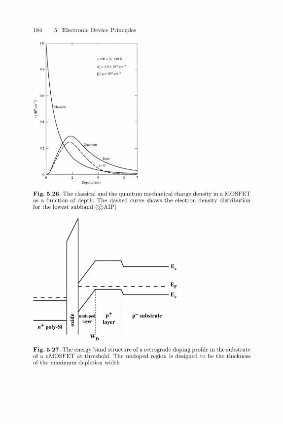
184 5. Electronic Device Principles
Fig. 5.26. The classical and the quantum mechanical charge density in a MOSFETas a function of depth. The dashed curve shows the electron density distributionfor the lowest subband ( c©AIP)
p– substratep+
layerundoped
layern+ poly-Si
EF
Ec
Ev
oxid
e
WD
Fig. 5.27. The energy band structure of a retrograde doping profile in the substrateof a nMOSFET at threshold. The undoped region is designed to be the thicknessof the maximum depletion width

5.3 Metal Oxide Semiconductor Field Effect Transistors MOSFETs 185
doping profile (Fig. 5.27). This profile when designed correctly can eliminateall dopant fluctuation effects on the threshold voltage and is presently usedin most production MOSFET designs.
5.3.7 MOSFET Device Performance
Each year the gate length of MOSFETs is reduced. Therefore any deviceresults in this part of the book will be out of date before the publication ofthe book. It is informative to at least show some typical performance dataas this should only have to be scaled to gain the performance for a differenttechnology node. Fig. 5.28 shows the current-voltage plots for both a nMOSand (upside down) pMOS at the 0.13µm technology node. It should be clearthat there is a difference in the on current, Ion of about a factor of 2.5 whichis related to the holes having a mobility lower than the eletrons by the samefactor. The subthreshold plots for these transistors are shown in Fig. 5.29where the Ioff current of 3 nA per µm is marked for a source-drain voltageof 1.5V.
Fig. 5.28. IV characteristics from a 0.13 µm CMOS technology produced by Intelwith a 1.5 nm thick oxide ( c©Intel)
5.3.8 Silicon On Insulator (SOI)
Silicon-on-Insulator or SOI is now in production for a number of differentproducts including microprocessors for portable devices and low power ap-plication specific integrated circuits (ASICs). A good example is the IBMPowerPCTM microprocessor many designs of which are now manufacturedusing a full SOI substrate to reduce the power dissipation for portable ap-plications. There are a number of different types of SOI devices which can

186 5. Electronic Device Principles
Fig. 5.29. Subthreshold characteristics from a 0.13 µm CMOS technology producedby Intel with a 1.5 nm thick oxide ( c©Intel). Ioff is marked with the 3 nA µm−1 linewhere the subthreshold slopes of the n- and p-MOS transistors intersect at V =0V
be fabricated and are aimed between two different opposite extremes (Fig.5.30). The first is the reduction of the substrate capacitance by the incorpo-ration of the buried oxide layer. This can either be transferred into a circuitimprovement in speed of around 30% or more commonly is used to reduce thepower dissipation of a circuit by around 30% compared to a bulk -Si substratewafer. The main application for such devices has been low power portabledevices such as mobile phones, laptop computers and personal digital assis-tants (PDAs). The second extreme is related to the inability to switch thechannel of a MOSFET off as the channel length approaches sub-20nm or sodimensions. This is predominantly related to the high doping required in bothcontacts and the substrate and at some gate length, the scaling relations dis-cussed in Sect. 5.5.3 break down. By producing a partially or fully-depletedthin Si channel on top of oxide, either a back gate, double gate (Fig. 5.30(c))or wrap-around gate (termed frequently as a FinFET)(Fig. 5.30(d)) can befabricated which allows the channel to be completely depleted by the gates,thereby switching the transistor off.
There are two main techniques for the formation of SOI wafers. The firstis termed Separation by IMplantion of OXygen (SIMOX) and involves theimplantation of oxygen to the required depth in a bulk Si substrate beforethe substrate is heated to ∼ 1250 C. At this temperature SiO2 is formed andmost of the implantation damage is annealled out. The second is produced bywafer Bonding and Etch back SOI (BESOI). Here two wafers have thermaloxides grown on the surface and are then bonded together and annealled athigh temperature (>1100 C). One of the wafers is then thinned by eitheror a combination of chemical mechanical polishing and chemical etching. A

5.3 Metal Oxide Semiconductor Field Effect Transistors MOSFETs 187
SiO2
Si substrate
poly
silicide silicidep-Sin++ n++
SiO2
Si substrate
poly
silicide silicidep-Sin n
(a) (b)
SiO2
p-Si substrate
poly
silicide silicidep-Sin n
(c)
siliciden
(d)
n++SiO2
Si substrate
p p
n++ n++
gate
Fig. 5.30. (a) A partially depleted SOI MOSFET where the Si body above theoxide is only partially depleted by the gate electrode. (b) A full depleted SOIMOSFET where the gate electrode can fully deplete the Si body above the oxide.(c) one design of double gate MOSFET using SOI. (d) A wrap around gate orFinFET transistor
thin SiGe layer is frequently used as an etch stop layer allowing fast etches tostop accurately close to the required thickness for the thin top silicon layer.There is also a technique called Smart-CutTM which implants hydrogen intothe wafer. On annealling the hydrogen layer forms bubbles and the wafer canthen be easily fractured along these bubbles before being polished.
The general SOI transistor has smaller parasitic capacitances, smallersource/drain leakage and are less immune to soft errors caused by alpha par-ticles. SOI transistors also allow higher speed and lower power consumptionthan bulk Si devices. In particular the buried oxide eliminates many leakagepaths. The major problem with SOI apart from the higher substrate cost isthe poor thermal conductivity of the SiO2 layer that can produce thermalproblems. There are two main type of standard MOSFETs which can be pro-duced on SOI substrate. The first is a partially depleted body device (Fig.5.30(a)). In this device the silicon layer above the oxide is thick and can-not be fully depleted by the transistor gate. One potential problem that canoccur with this transistor is the ”body” of silicon between the two contactscan become charged which may change the threshold voltage and change thedigital on and off state voltages. This is termed the ”body effect” and maybe removed by arrange an earth contact to the body silicon.
The second type of standard SOI transistor is the fully depleted transistor(Fig. 5.30(b)). Here the body is so thin that there is also depletion from thebottom side due to the potential from the p-substrate. The threshold implantfor the body is set so that the top gate can fully deplete the silicon bodybetween the contacts when the transistor is switched off. As transistor gatesare reduced below about 50 nm, it becomes substantially more difficult to

188 5. Electronic Device Principles
switch the transistor off as the high doping levels between the two contactscannot be achieved to deplete the channel. The fully-depleted SOI MOSFETcan solve this problem by the additional depletion from the bottom interface.As gate-lengths are reduced below about 20 nm, this problem of switching atransistor off becomes worse and two gates such as Fig. 5.30(c) or a wraparound gate or FinFET as Fig. 5.30(d) may be required.
5.4 Further Reading
1. Y. Taur and T.H.Ning, Fundamentals of Modern VLSI Devices, CUP,Cambridge (1998)
2. S.M. Sze, The Physics of Semiconductor Devices, 2nd Edition, John Wileyand Sons, New York (1981)
3. S.M. Sze, Modern Semiconductor Device Physics, John Wiley and Sons,New York (1998)
4. C.Y. Chang and S.M. Sze, ULSI Devices, John Wiley and Sons, NewYork (2000)
5. S.M. Sze, Semiconductor Devices: Physics and Technology, 2nd Edition,John Wiley and Sons, New York (2002)

6. Heterostructure Bipolar Transistors - HBTs
The first major application for which SiGe heterolayers has been used is theheterostructure bipolar transistor or HBT. The original idea on the HBT ac-tually appears in the original patent for the transistor. Herb Kroemer latterpublished a paper with more details about wide gap emitters along with theidea of grading the bandgap of the base to accelerate the carriers across thebase. In the wide band gap emitter concept the top layer (emitter) consistsof a material with wider band gap (e.g. GaAlAs) than in the underlying base(e.g. GaAs) and collector layers (table 6.1). A direct transfer of this concept toSi based electronics failed because of material problems. The most promisingcandidates, amorphous silicon (a-Si) and silicon carbide (SiC) suffered fromemitter resistance and interface quality problems, respectively. The corre-sponding principle to the wide band gap emitter is the small band gap base(table 6.1) which contains two heterointerfaces and hence is also called doubleheterostructure bipolar transistor (DHBT). Silicon germanium is an appro-priate material for the DHBT concept. Mainly it is used as pseudomorphicSiGe (strained SiGe, unstrained Si).
Table 6.1. Layer structure and material choice for the wide band gap emitter HBTand the small band gap base DHBT. The material A is with the wider band gapthan the material B. The usual emitter configuration is assumed. Heterointerfacesare marked with HI.
Layer HBT (wide gap emitter) DHBT (small gap base)
emitter A A——————— HI ——————— HI1
base B B——————— HI2
collector B A
substrate B A
The first patent on a SiGe/Si small band gap base HBT was filed in1977 by E. Kasper and P. Russer. The first SiGe HBTs had to wait until1987 when the epitaxial growth became good enough to attempt transistors.Numerous other papers and groups followed. The first circuits were being

190 6. Heterostructure Bipolar Transistor
sold in the market place in 1999, a little over a decade after the first deviceswere fabricated.
n-Si n-Si n-Si n-Si n-Si n-Si
Ge
cont
ent
p-Si1-xGex p-Si1-xGex p-Si1-xGex
(a) (b) (c)
emitter base collector emitter base collector emitter base collector
Ban
dgap
base
Fig. 6.1. A schematic diagram of the Ge profile in different types of HBTs and theresulting bandgap energy. (a) a box profile, (b) a graded or triangular profile and(c) a trapezoidal profile which is a combination of (a) and (b)
There are three main types of base design in SiGe HBTs as shown inFig. 6.1: (a) box like (b) graded base and (c) trapezoidal base (a combina-tion of the first two). Strictly speaking, a HBT is engineered to have a largerbandgap in the base at the emitter-base junction. Therefore only the box andtrapezoidal profiles are true HBTs and the linearly graded profile is a gradedbase transistor. Each design has its own merits and problems. The precisedesign that will be used will depend on the application and the other com-ponents in the circuits. It is worthwhile deriving the important parametersof the HBT designs before comparing the advantages and disadvantages. Wewill only derive the box and linear graded parameters. This will demonstratethe two extremes and the trapezoidal profile results are a mixture betweenthe two.
Figure 6.2 shows the band structure for a HBT. For the HBT, the diagramshows that the barrier for electrons travelling from the emitter to the collectoris reduced. The additional valence band discontinuity between the base andthe emitter reduces hole injection from the base into the emitter. One wouldtherefore expect the collector current and hence the gain of the transistor tobe much higher than a standard silicon bipolar transistor.
Figure 6.3 shows the band structure for a linearly graded base transistor.The linear grade in the base accelerates the electrons across the base but theemitter base junction remains identical to a standard silicon homojunctiontransistor. It is clear that the electric field accelerating carriers across the basewill reduce the base transit time and hence increase the cut-off frequency ofthe transistor. The effect of the grading on the other parameters is not asobvious from the band structure and will require solutions of the appropriateequations.
Most of the important parameters in HBTs may be calculated by simplyreplacing the effective intrinsic carrier concentration in the base from thebulk silicon expression (Sect. 5.2) to one which accounts for the SiGe in the

6. Heterostructure Bipolar Transistor 191
Ec
holes
electrons
BJT
HBT
∆Eg
Ev
emittern+ Si
basep-Si1-xGex
collectorn+ Si
EFC
EFB
EFEqVBE
qVBC
Fig. 6.2. A schematic diagram of the band structure for a Si bipolar transistor(BJT - dotted lines) and a box Ge profile HBT
Ec
holes
electrons
BJT
Linear grade
emittern+ Si
basep-Si1-xGex
collectorn+ Si
∆Eg
EvEFC
EFB
EFEqVBE
qVBC
Fig. 6.3. A schematic diagram of the band structure for a Si bipolar transistor(BJT - dotted lines) and a linearly graded Ge-base profile transistor
base and then solving the formulae. The effective intrinsic carrier density inthe base is given by (neglecting differences in the effective densities of statesbetween Si and SiGe)
n2ieB (SiGe) = n2
ieB (Si) exp[∆Eg
kBT
]box profile (6.1)
n2ieB (SiGe) = n2
ieB (Si) exp[∆Eg
kBT
z
WB
]linear grade (6.2)

192 6. Heterostructure Bipolar Transistor
where ∆Eg is the bandgap reduction for the HBT and the maximum bandgapreduction for the linear graded base.
The basic advantage of the HBT is given by the different barrier forelectron and hole injection which allows the device designer more freedom.A SiGe HBT with the same doping profile as a Si BJT (bipolar junctiontransistor) would exhibit a higher current gain, β0, than its Si counterpartalone. We will, therefore, call this Ge box profile HBT design as the highcurrent gain HBT in the following section. Of significantly more practicalimportance is producing a transistor design where the current gain can betraded off for the high speed. On this high speed design we will first discussthe SiGe HBT properties.
6.1 Trade-off between current gain and speed
From the introduction the reader will understand that the SiGe-HBT whichhas the same doping and widths as the Si-BJT is superior to the latter incurrent gain. But the success of the SiGe-HBT is based on a trade off betweencurrent gain and speed and the understanding of the real HBT is often blurredby this trade off. We start with explaining the speed disadvantages of the Si-BJT and continue with analysing the fundamental steps in the mentionedtrade off.The fundamental speed limit of the Si-BJT is given by its base design. In orderto get a reasonable current gain β0 the base doping N
(B)A has to be roughly
two orders of magnitude lower than the emitter doping N(E)D . The limited base
doping levels of about 1018/cm3 with the thin base thickness (around 100nm)result in a low base conducitivity measured as a high base sheet resitivityRShB of around 4kΩ/sq. A high base resistance RB influences directly themaximum oscillation frequency fmax but also fT measurements indirectlybecause with high base resistances the base signals are reduced which leadsto current crowding at the emitter edges except in emitter stripes with verylow stripe width bE . The progress in Si-BJT speed was therefore linked tothe shrinking of lateral dimensions allowing higher base sheet resistivities toobtain the same base resistances .With SiGe-HBTs the base doping N
(B)A is not more limited by the obtainable
current gain because gain is produced by the E-B heterointerface. The tradeoff follows the scheme given below
• Step1: Increase of the base doping level N(B)A by typically an order of
magnitude. The upper limit of the increase is given by exp(∆Eg/kBT )but practically often the increase is limited by the outdiffusion of boronin following process steps. Directly opposed high doping levels in a p-njunction lead to tunneling currents which are suppressed by a thin lowdoped emitter (LDE) between base and usual high doped emitter (HDE).

6.2 The High Speed SiGe HBT 193
This LDE is frequently unmentioned and hidden in the specific processsequence of the producer.
• Step2: Reduction of the base thickness wB by a factor two to five. Thecorresponding decrease of the base transit time τB (mainly following a w2
B
law) increase both, fT and fmax. The reduction of τB lets the collectortransit time τC as dominating time constant in many HBT designs.
• Step 3: Reduction of the collector thickness wBC decreases the collectortransit time τC . The gain in τC is partly compensated by the inherent(RE+RC)CBC time constant which increases with wBC (CBC∼1/wBC).The optimum design depends on the technological parameters emitterand collector resistance, and base area ABC . But, the thinner collectorreduces the collector-base breakdown voltage BVCB0 and the collector-emitter breakdown voltage BVCE0.
• Step 4: Increase of the collector doping N(C)D .
The collector width wBC is depleted under operation conditions (the un-depleted collector width would otherwise increase the collector resistance).The thinner collector width allows higher collector doping levels to be de-pleted which in turn shifts the modified Kirk effect to higher current levels.Higher current levels reduce the input time delay (∼1/IC). The Kirk effectlimits ultimately the useful current density by an effective base extensioninto the collector above a critical current value. In a DHBT the base ex-tension is additionally influenced by the second interface, therefore it istermed modified Kirk effect.
Table 6.2. HBT layer design steps for trade off β vs fT (see text for more details).
No step advantage disadvantage
1 N(B)A ↑ RShB↓ ,fmax↑ tunneling circuits
1a LDE avoids tunneling
2 wB↓ τB → fT ↑, fmax↑3 wBC↓ τB → fT ↑, fmax↑ τRC↑, BVCE0↓4 N
(C)D ↑ Jcrit↑, fT ↑, fmax↑
6.2 The High Speed SiGe HBT
In order to simplify the considerations but without loss of generality weassume an emitter up finger geometry (Fig. 6.4) with abrupt and flat dopingand Ge profiles (Fig. 6.5). The emitter finger with area AE (finger length lEtimes finger width bE) defines the current injection IE = AE × JE . For high

194 6. Heterostructure Bipolar Transistor
speed operation the current density JE∼= JC is driven to high values near
the onset of the modified Kirk effect. The corresponding power consumptionP in the transistor heats the transistor above the ambient temperature (selfheating). Transistors with smaller finger width, bE , may be driven to highercurrent densities for the same junction temperature. On one side the basecontact is typically self-adjusted so that the sum of the base finger width,bB, and emitter finger width, bE , roughly define the collector finger width,bC
∼= bE + bB. Another frequently used design has the base contacts on bothsides of the emitter which results in a smaller base resistance, RB, but highercollector-base junction capacitance because then the collector finger width isroughly given by bC
∼= bE +2bE. The collector is contacted via a highly dopedsubcollector (typical sheet resistivities of 10 to 25 Ω cm2) which is fabricatedas a buried layer before the epitaxy of the n-collector. The collector contact isseparated from the base contact by a distance s to reduce capacitive couplingbetween the input signals at the base and the output signals at the collectorin the common emitter circuit.
Fig. 6.4. A sketch of the SiGe-HBT design for an emitter (E) up geometry with abase contact on one side (B). The n-collector (C) is contacted via a highly dopedn+-subcollector. Regions with n-doping are blue coloured (n+ emitter and n+ sub-collector darkblue; n-collector light blue) and the p-SiGe region is coloured red
The vertical structure consists of a two stage emitter, the p-type SiGebase and the collector-subcollector sequence. The high doped emitter (HDE)provides the reserve of electrons important for injection with high currentgain, β0, whereas the emitter-base junction capacity CBE and the amount ofthe trap assisted tunnelling current (excess current) are determined by thelow doped emitter (LDE). The p-doped SiGe base is cladded on both sidesby intrinsic or n-type SiGe spacers to avoid out diffusion of the p-dopinginto the Si-layers which has very detrimental effects on the HBT function.The n-collector is optimally designed to be depleted under the operatingvoltage VCE . A thicker collector would increase the collector resistance RC

6.2 The High Speed SiGe HBT 195
and a thinner collector would increase the base-collector capacitance CBC .The sub-collector functions as in a BJT with the sheet resistance RSh asmost important property. For the chosen flat profile the sheet resistance isgiven by
(RSh)−1 = q
∫z
n(z)µ(z)dz = qND,SubCWSubCµp (6.3)
where ND,SubC is the donor concentration in the subcollector with width,WSubC .
Table 6.3. Fundamental differences in the designs of a high speed Si-BJT and aSiGe HBT.
typical base typical collectorLDE SiGe doping width doping
Si-BJT no no 1018 cm−3 100 nm 3 × 1016 cm−3
SiGe-HBT yes yes 1019 cm−3 30 nm 3 × 1017 cm−3
Fig. 6.5. A schematic profile of the doping and Ge concentration (drawn in thez-direction below the emitter contact). The following doping regions are shown:High doped emitter (HDE), low doped emitter (LDE), SiGe layer (SiGe), p-dopedSiGe base (B), collector (C) and subcollector (Sub C). The Ge concentration isdecreased by a factor 10 to fit into the figure
This general doping structure is similar to that of a Si BJT with the char-acteristic differences summarised in Table 6.3. The most important differenceconcerns the base structure. The base contains a SiGe alloy, its p-doping ismuch higher and the thickness is considerably thinner. The higher doping

196 6. Heterostructure Bipolar Transistor
and lower thickness of the base follows from the trade off between the currentgain and speed. The changes in the emitter and collector are consequencescaused by the requirements to avoid an increase in tunnelling across the base-collector junction and to reduce equivalently the collector transit time.The actual thicknesses and concentration levels are dictated by the require-ments for current gain, speed, breakdown voltages and by the technologicalconstraints from growth and device processing. As an example we choose ahigh speed HBT with low breakdown voltage BVCE (collector-emitter volt-age) and a moderate speed HBT with higher breakdown voltage.
Table 6.4. Layer structures of two different HBT transistors (HBT1 high speedfT =220 GHz, BVCE=1.8V, HBT2 moderate speed fT =60 GHz, BVCE=6V).
Structure No. thickness doping Ge content(nm) (1017 cm−3) (%)
Subcollector 1,2 4000 n, 50 -
Collector 1 50 n, 4 -2 250 n, 0.4
Base 1 12 p, 80 282 27 p, 50 18
LDE 1 20 n, 4 -2 100 n, 10
HDE 1,2 200 n, 200 -
As shown by these examples the thicknesses of the base and collector areshrunk to get the higher speed. The collector thickness shrinkage resultsin lower breakdown voltages, BVCE . As general in bipolar transistors thecollector-emitter breakdown voltage is a factor of 2-3 lower than the corre-sponding collector-base breakdown voltage, BVCB because of the feedbackfrom impact ionised holes.
For the analysis of the high frequency behaviour of the HBT an investiga-tion of the current dependence of the transit frequency is the most importantstep. For this we have to rearrange the single components of the emitter col-lector transit time, τEC , (5.86). Assuming that τE2 may be neglected andusing (5.94) and the saturation velocity, vsat (see Fig. 3.31), we obtain
12πfT
= τEC
=W 2
B
2Dn+
WB
ve+
WBC
2vsat+ CBC · (RE + RC) +
kBT
qIC(CBE + CBC) (6.4)

6.2 The High Speed SiGe HBT 197
where τB and τhc are current independant, τC is split into a current dependantpart and a RC load time τRC = CBC(RE +RC). From (6.4) one would expecta linear plot of τEC vs 1/IC (Fig. 6.6). Indeed the linear fit is very goodup to high current densities where deviations by the modified Kirk effectlead to a steep increase in the transit time. The Kirk effect in a bipolartransistor is caused by the base extension under high current densities. In aHBT the BC heterojunction strongly influences the current flow. We namethis the modified Kirk effect because of the similar results as in the originaldescription. In the given example the fixed inner transit time is roughly 0.6 pswith about 0.2 ps for τB, τhc and τRC , respectively. From the slope of the linearfit a capacitance CBE + CBC of 12.2 fF/µm2 is extracted from which, in thegiven geometry, one third is attributed to CBC . The attainable minimumtransit time, τmin, is limited to values above the fixed inner transit timebecause of the modified Kirk effect which limits the current density to abouta critical current density of
Jcrit = qNDCvsat (6.5)
The critical current density Jcrit is 6.4× 10⁵ Acm−2 for the collector dopingNDC of 4 × 1017 cm−3.
The transit frequency fT is not dependant on the base resistance RB
because for the current gain measurement a base current modulation is givento the inner transistor. For the power gain the maximum oscillation frequencyfmax is the corresponding frequency limit which is strongly influenced by theloading of the capacitance, CBC , via the base resistance, RB. Rewriting (5.98)gives
fmax
fT=
12
√τEC
RBCBC(6.6)
which means a high transit frequency, fT , and a low RBCBC time constant areimportant for a high oscillation frequency. Let us give a simplified assessmentof the order of magnitude for the time constant RBCBC . For this we assumethe geometry of Fig. 6.4, a base contact with bB = bE and a simplified modelof the base resistance RB which contains an area proportional to the externalbase conductance
1RBe
=(bE · lE)
ρCB(6.7)
and an inner base resistance, RBi
RBi = RShB · bE
6lE(6.8)
which is proportional to the base sheet resistance, RShB. The collector-basecapacitance, CBC , is given by

198 6. Heterostructure Bipolar Transistor
Fig. 6.6. The inverse transit frequence 1/2πfT =τEC versus inverse current 1/IC .Numerically calculated (BLAZE) transit frequency for a 1 µm×1µm emitter fingerwith the structure given in table 6.4 (high speed transistor)
CBC = 2 · (bE · lE)ε0εSi
WBC(6.9)
In this simplified model the transit time constant RB · CBC is obtainedby
RB · CBC = (2 · ρCB +13RShB · b2
E) · (ε0εSi
WBC) (6.10)
This time constant depends both on the vertical structure of the devicewhich determine WBC and the base sheet resistance, RShB, but also on thelateral structure which defines bE and ρCB (remark: from (6.7) ρCB containsnot only the specific contact resistance of the base but also the other area de-pendant parts of the external base resistance). The ultimate fmax which maybe obtained is given by neglecting the external base resistance contributions(ρC → 0).
fmax <1bE
√fT · wBC · 3
4π · RShB · ε0εSi(6.11)
From the device technology viewpoint a small emitter finger (bE ↓) isimportant to obtain high fmax values.

6.3 The Linear Graded Profile 199
6.3 The Linear Graded Profile
The saturated collector current density requires (5.68) to be modified to
JC0 (SiGe) =q∫WB
0pp(z)
DnB(SiGe)n2ieB
(SiGe)dz
(6.12)
Let us assume that the doping profile, pp is near constant throughout thebase in both transistors and approximately equal to the doping density inthe base NB. Therefore (6.12) simplifies to
JC0 (SiGe) ≈ qDnBn2iB (Si)
NBWBexp
[∆Eg
kBT
]box profile (6.13)
for the HBT and the linear graded transistor becomes
JC0 (SiGe) ≈ qDnBn2ieB (Si)
NB
1∫WB
0exp
(−∆Eg
kBTz
WB
)dz
linear grade
=qDnBn2
ieB (Si)NBWB
∆Eg(SiGe)kBT
1 − exp(−∆Eg(SiGe)
kBT
) (6.14)
Since the base currents are approximately similar between the SiGe and Sibase transistors, it is the collector currents which produce the major changes.Therefore comparing the collector currents between the Si and SiGe transis-tors we find
IC (SiGe)IC (Si)
= exp[∆Eg
kBT
]box profile (6.15)
IC (SiGe)IC (Si)
=∆Eg
kBT
1 − exp[−∆Eg
kBT
] linear grade (6.16)
It is therefore the collector currents which have the biggest effect on thegain. The gain for a box profile transistor is modified using (5.75) and (5.79)to produce
β (SiGe)β (Si)
= exp[∆Eg
kBT
]box profile (6.17)
β (SiGe)β (Si)
=JC0 (SiGe)JC0 (Si)
=∆Eg(SiGe)
kBT
1 − exp(−∆Eg(SiGe)
kBT
)linear grade (6.18)
200 6. Heterostructure Bipolar Transistor
To calculate the Early voltage, (5.74) must be used along with substitutingthe intrinsic electron concentrations in the SiGe bases from (6.1) and (6.2).Therefore
VA (SiGe) qDnBn2ieB
(Si)CBC
WB∫0
NB (z)DnB (z)n2
ieB(SiGe, z)
dz (6.19)
must be solved for the two cases to give
VA (SiGe) VA (Si) box profile (6.20)
VA (SiGe) qNBWB
CBC
kBT
∆Eg
[exp
(∆Eg
kBT
)− 1
]ABC (6.21)
linear grade
Therefore there appears to be no change to the Early voltage in an HBTwhile the linear graded transistor has a nearly exponential change. In reality,however, the Early voltage in typical box profile HBTs will be greater thana normal silicon bipolar transistor because VA is proportional to base dop-ing which can be increased in a box profile HBT without trading off otherparameters. The small bandgap has no role to play in modifying the Earlyvoltage of a HBT.
To find the base transit time, (5.92) must be rewritten as
τB (SiGe) ≈WB∫0
n2ieB(SiGe, z)
NB (z)
WB∫x
NB (z′) dz′dz
DnB (z′)n2ieB(SiGe, z′)
(6.22)
Substituting (6.1) and (6.2) produces the following results
τB (SiGe) = τB (Si) box profile (6.23)
τB (SiGe) ≈ W 2B
DnB
kBT
∆Eg
(1 − kBT
∆Eg
[1 − exp
(−∆Eg
kBT
)])linear grade (6.24)
Since from (5.91) the emitter transit time is inversely proportional tothe gain of the transistor ((6.17) and (6.18)), this value will be reduced inboth types of transistor. Therefore the cut-off frequency will be increased inboth the box profile HBT and the linear graded base transistors compared tostandard silicon bipolar devices. For the box profile HBT, the improvement infT is predominantly due to the exponential increase in gain with decreasingbandgap reducing τE . For the linearly graded base, the in-built electric fieldfrom the Ge profile reduces τB while the nearly linear increase in gain withreducing bandgap will reduce τE thereby increasing fT . The comparisons

6.3 The Linear Graded Profile 201
made above are given with the same doping profiles for the Si and SiGetransistors. In real designs the high current gain of the HBT is traded againsthigher base doping NB (lower base resistance) and smaller base width WB
(lower base transit time).
Table 6.5. A comparison of performace gains for HBTs and linearly graded SiGebase transistors (same dopant profile as a Si bipolar function transistor)
Parameter High gain Linear gradedSiGe HBT SiGe base
n2iB(SiGe)n2
iB(Si)exp
[∆Eg
kBT
]exp
[∆Eg
kBTz
WB
]JC(SiGe)
JC(Si)exp
[∆Eg
kBT
]∆Eg
kBT(1−exp
[−∆EgkB T
])β(SiGe)
β(Si)exp
[∆Eg
kBT
]∆Eg
kBT(1−exp
[−∆EgkB T
])VA(SiGe)
VA(Si)1 kBT
∆Eg
(exp
[∆Eg
kBT
]− 1
)β(SiGe)VA(SiGe)
β(Si)VA(Si)exp
[∆Eg
kBT
]exp
[∆Eg
kBT
]τB(SiGe)
τB(Si)1 2kBT
∆Eg
(1 − kBT
∆Eg
(1 − exp
[∆Eg
kBT
]))τE(SiGe)
τE(Si)∼ exp
[∆Eg
kBT
]∼ kBT
∆Eg
(1 − exp
[∆Eg
kBT
])
The great advantage of the addition of Ge into the base of either the boxprofile HBT or the linear graded base transistor is the additional flexibilityin device performance to optimise circuit performance. For digital bipolarcircuits, the most important parameters are the circuit switching speed andthe power dissipation. Therefore minimising the base resistance, the base-collector capacitances and all parasitic capacitances in the device or circuitincreases the performance more than optimising other parameters. Analoguecircuits will also benefit from optimisation of the important parameters in thedigital circuit. The main parameters to optimise are the cut-off frequency, themaximum frequency of oscillations, the base resistance and the Early voltage.In both cases the reduction of the base resistance becomes important. Thisrequires increasing the doping density in the base. The easiest way to achievethis is to trade off the extra gain that a SiGe base transistor gives for increaseddoping density in the base and therefore lower base resistance. Table 6.5 shows

202 6. Heterostructure Bipolar Transistor
a summary of the performance of SiGe box profile HBTs and linearly gradedbase transistors compared to standard silicon bipolar devices.
Fig. 6.7. A Gummel plot showing the typical difference between a Si bipolarand a SiGe HBT device. The collector current for the SiGe linear graded baseis approximately 4.5 times that for the Si bipolar. ( c©IEEE)
6.4 SiGe HBT Device Performance
In this section some experimental data from both Si bipolar and SiGe HBTtransistors will be reviewed. Most of the data is from IBM using a 0.5µmBiCMOS process using 200mm wafers and UHVCVD growth of the SiGebase. The SiGe base profile is a linear grade from 0 to 15% over 100 nm. Whilethese are not the most aggressive or highest performance devices around theyhave been compared with comparable Si bipolar devices produced using thesame process and therefore illustrate the performance differences between Siand SiGe transistors very nicely. Box shaped transistors with their highercurrent gain differ in several parameters (emitter doping, base doping, basewidth) from their silicon counterparts and the influence of one parameter isnot as easily observed.
Figure 6.7 shows a Gummel plot for both the Si and SiGe devices withall other major common parameters constant (at least as best is possiblefor the different types of bipolar transistors). While the base currents arealmost identical, the increase in the SiGe collector current is very obvious.The common emitter configuration characteristics of a similar device with adifferent area is shown in Fig. 6.8.
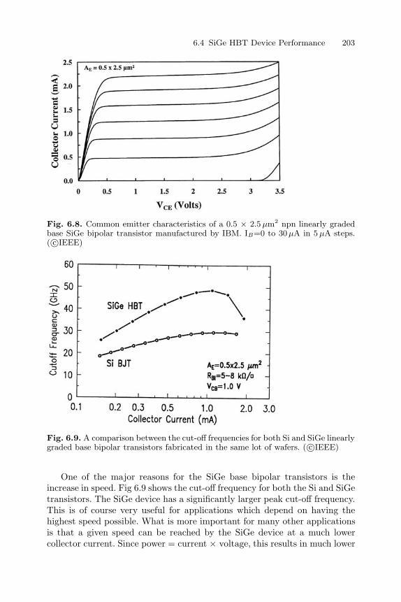
6.4 SiGe HBT Device Performance 203
Fig. 6.8. Common emitter characteristics of a 0.5 × 2.5 µm2 npn linearly gradedbase SiGe bipolar transistor manufactured by IBM. IB=0 to 30µA in 5 µA steps.( c©IEEE)
Fig. 6.9. A comparison between the cut-off frequencies for both Si and SiGe linearlygraded base bipolar transistors fabricated in the same lot of wafers. ( c©IEEE)
One of the major reasons for the SiGe base bipolar transistors is theincrease in speed. Fig 6.9 shows the cut-off frequency for both the Si and SiGetransistors. The SiGe device has a significantly larger peak cut-off frequency.This is of course very useful for applications which depend on having thehighest speed possible. What is more important for many other applicationsis that a given speed can be reached by the SiGe device at a much lowercollector current. Since power = current × voltage, this results in much lower

204 6. Heterostructure Bipolar Transistor
Fig. 6.10. The cut-off frequency and fmax versus collector current for a lineargraded base SiGe bipolar transistor. ( c©IEEE)
Fig. 6.11. The ECL ring oscillator gate delay for a Si bipolar transistor and vari-ations in the Ge profile of SiGe base bipolar transistors. ( c©IEEE)
power consumption. Particularly for portable solutions such as mobile phones,it is this particular characteristic of the SiGe base bipolar transistor whichis most useful. For high speed applications, both fT and fmax are important.Both are plotted for a SiGe transistor in Fig. 6.10. This is a typical designfor a transistor where fmax is approximately 10 to 20% higher than fT .
All the figures above have been related to single devices but for applica-tions it is the circuit performance which matters. There are of course manydifferent types of circuit that can be built but so that general comparisons

6.4 SiGe HBT Device Performance 205
Fig. 6.12. fT characteristics for an IBM linear graded base SiGe bipolar transistorat various VCB for a 0.22 × 5 µm2 non-self aligned device ( c©IEEE).
can be made between technologies, there are a few standard circuit configura-tions which are used. One of the major test circuits for a bipolar technology isthe emitter common logic (ECL) ring oscillator gate delay which is shown forboth Si and SiGe technology in Fig. 6.11. At about 1mA switching current,the best SiGe base design has a average gate delay almost half that of theSi bipolar technology. The other way to compare the technology is to takea fixed gate delay for which the SiGe technology requires half the switchingcurrent of the Si bipolar circuit. This will translate into a SiGe linear basetransistor power dissipation which is approximately half that of the Si bipo-lar. The combination of bipolar devices with complementary MOS (CMOS)logic is termed BiCMOS. The availability of high speed HBTs with good βVA
product pushed strongly the introduction of BiCMOS circuits.The results above have shown some of the early production devices from
IBM but of course research has been continuing. In Fig. 6.12 one of the resultsfrom the literature is shown where the cut-off frequency has been increased to210GHz using a linear graded base SiGe technology with the base Ge contentvaried between 0 and 25%. The device is not self-aligned and so the fmax valueis relatively low in this particular device. It does show, however, that bipolartransistors with SiGe in the base can have operating parameters far above200GHz, an area which was previously only believed to be achievable usingIII-V technology.
As mentioned before a clear analysis of the frequency behaviour is givenby a plot of τEC=(2πfT )−1 versus (1/IC). For the three typical SiGe-HBTgenerations this analysis is done in Fig. 6.13. From the slope of the curves

206 6. Heterostructure Bipolar Transistor
Fig. 6.13. Analysis of the frequency behaviour by a plot of τEC=(2πfT )−1 versus(1/IC). For the three typical SiGe-HBT gemerations
one can immediately conclude about the capacity CBE + CBC of the dif-ferent transistors. The slope is given by Vt(CBE + CBC)yielding 38.5 fF,14.9fF and 5.3fF for the 1µm2 (fT =45 GHz), 0.26µm2(fT =120 GHz) and0.18µm2(fT =210 GHz) transistor, respectively. From exrapolation of theslope toward (1/IC)=0 the main contributions (τB+τC+τRC) to the cur-rent independent part of the time constant τECmay be assessed to be 3.0ps,1.1ps and 0.6ps, respectively. This demonstrates nicely the reduction of thetime constants in the subpicosecond regime obtained by decrease in baseand collector thickness. The onset of the Kirk effect (IC=2mA for all threetransistors with decreasing area) demonstrates the increasing critical currentdensity caused by the increased collector doping from 1017/cm3 to nearly1018/cm3.
6.5 Further Reading
1. Y. Taur and T.H.Ning, Fundamentals of Modern VLSI Devices, CUP,Cambridge (1998)
2. C.Y. Chang and S.M. Sze, ULSI Devices, John Wiley and Sons, NewYork (2000)
3. D.J. Paul, Semiconductor Science and Technology 19, R59 (2004)4. J.D. Cressler and G. Niu, Silicon-Germanium Heterojunction Bipolar
Transistors, Artech House, Norwood (2003)5. J. Eberhardt, E. Kasper, Solid-State Electronics 45, 2097 (2001)6. E. Kasper et al., Solid-State Electronics 48, 837 (2004)

7. Hetero Field Effect Transistors (HFETs)
The classical approach to heterostructure field effect transistors (HFET) isgiven both in III/V-materials and SiGe/Si by using modulation doped struc-tures (modulation doped FET-MODFET). These structures have proven car-rier confinement in quantum dots with improved mobility in two dimensionaltransport. These devices are also called HEMT (high electron mobility tran-sistor) or TEGFET (two dimensional electron gas FET). Silicon microelec-tronics driven are the more recent approaches to provide HFETs with insulat-ing gates as in a MOSFET and to combine n-channel and p-channel devicesas in a CMOS logic. Further on, one hast to consider the specific band order-ing in the SiGe/Si system to understand the differences to the approaches inIII/V-systems. Let us first remember the band ordering in SiGe/Si as func-tion of the strain situation (Fig.7.1). In the technologically simplest case (a)a pseudomorphic, thin layer SiGe is compressively strained on a Si substrate.Then electrons are more or less not influenced by the heterointerface (theconduction band offset ∆EC is below ±20meV, the sign of the offset is underscientific debate since more than a decade). The holes are confined to the lowband gap side SiGe (∆EV
∼= 0.7x eV, x Ge content). The electronic nature ofthis interface (SiGe strained) is between type I and type II. With reversedstrain, that means a tensile silicon layer grown on a virtual substrate withunstrained SiGe layer on top, the electronic nature of the interface switch toa type II (case (B) in Fig. 7.1) where the electrons are confined to the largeband gap semiconductor (Si) and the holes to the small band gap SiGe.
With this knowledge in mind let us now discuss the possible routes for acomplementary, insulated gate HFET logic on silicon (Tab.7.1).
The easiest integration is promised by the first route via pseudomorphicSiGe. The principle scheme is shown in Fig. 7.2. The n-MOS is made in Sias usual. The SiGe p-MOS is made in areas where selectively a thin SiGe/Silayer stack is deposited on top of the Si-substrate. The Ge-content is low(around x=0.15), the improvement in the p-channel stems from the valenceband splitting (heavy, light holes) and the better carrier transport in the 2Dhole gas.

208 7. Hetero Field Effect Transistors (HFETs)
Eg
EV
EC
EV
Si SiGe
Eg
EV
EC
EV
SiSiGe
EC
Fig. 7.1. Band ordering of (a) compressively strained SiGe on unstrained Si, (b)tensile strained Si on unstrained SiGe
Table 7.1. Main routes to hetero (CMOS) FET circuits.
Route p-channel n-channel Remarks
Pseudomorphic strained SiGe unstrained Si ⊕ Easy integrationSiGe (compression) (conventional p-SiGe and n-Si
n-MOS) only p-channelimprovement (10-30%)
strained Si strained Si strained Si ⊕ moderate p and(tension) (tension), n-channel improvementson SiGe, electrons jumpholes are only into Si virtual substrates,confined by strong (type II) parallel p-channelelectric fields to (SiGe)a Si channel
double channel strained SiGe or Ge strained Si ⊕ Ultimate, symmetric(compression), (tension), p- and n-channel,buried p-channel surface High improvements
n-channel High Ge content,high strain,virtual substrate,processing withlow temperature budget
In the strained Si route a tensile strained surface layer is provided forboth, holes and electrons. The electrons like to jump into strained Si, theholes have to be bound by strong vertical gate fields and tend to create par-asitic parallel channels in underlying SiGe layers. The standard approach togenerate tensile strain in Si is by a virtual substrate (Fig.7.3) composed of arelaxed SiGe layer on a Si-substrate.The strain can be alternatively transferred from a virtual substrate to a SOI-wafer (silicon on insulator) or generated by nanostructures (e.g. Ge islands or

7. Hetero Field Effect Transistors (HFETs) 209
S
G
D
SiGe
n-well
p p+ +
S
G
D
n n+ +
p-Si
gate metal
insulator
Fig. 7.2. Scheme of the pseudomorphic SiGe HFET (CMOS) route
implants). An unique solution would be provided by a double channel config-uration, especially when high Ge content alloys or pure Ge for the p-channelis foreseen.
S
G
D
n-well
p p+ +
S
G
D
n n+ +
p- Si
relaxed SiGe
strained Si strained Si
Fig. 7.3. Scheme of the strained Si CMOS route
All know semiconductors (with bandgaps large enough for room tempera-ture operation) suffer from hole mobilities much lower than those of the elec-trons, only Ge has hole mobilities (µp in undoped Ge is 1900cm2/V s) equallyhigh than the mobilities of electrons in Si (µn in undoped Si is 1450cm2/V s).This heterostructure couple offers the ultimate symmetric CMOS structurewith equally high electron and hole mobilities. The strain in such structure(Fig.7.4) can even further enhance the mobility. The electrons (type II inter-face) move in the tensile strained Si, the holes in the compressively strainedGe. The technological barriers for realisation of these high performance dou-ble channel CMOS are large and require considerable research effort to over-come. Main obstacles are growth of high quality virtual substrates with Ge-content 0.5 or more, the high strain in sub 10nm layers, the processing of Geand strained Si/Ge and the combination with high-k dielectric gate materi-als.In the following the vertical gate arrangement, the strained Si-MOS and theMODFET results are discussed in more detail.

210 7. Hetero Field Effect Transistors (HFETs)
Si-substrate
relaxed SiGestrainadjustment
virtualsubstrate
Si-substrate
relaxed SiGestrainadjustment
virtualsubstrate
Fig. 7.4. Double channel HFET (CMOS). Scheme of the layer structure
7.1 Vertical Heterojunction MOSFETs
n+-Si
n+-Si
p-Si
source
drain
gate
p-Si substrate
oxide
p+-Si
p+-Si
n-Si
source
drain
gate
p-Si substrate
oxide
2DEG2DHG
Fig. 7.5. An example of a p-VMOS on the left and a n-VMOS on the right
Vertical sidewall MOSFET designs were very popular when it was thoughtthat optical lithography could not be used much below 0.25µm. The greatadvantage of a vertical FET is that the vertical dimensions of a FET can beeasily controlled down to sub-10 nm. Already gate oxides on MOSFETS arebelow 1.5 nm in production while the lateral gate-lengths are 60 nm demon-strating how the vertical dimensions of standard MOSFETs are typically 100times smaller than the lateral lithographically defined dimensions. A typicaldevice layout is shown in Fig. 7.5. The figures also demonstrate the major dis-advantage of the vertical MOSFET concept. Since the gate is not self-alignedwith the channel, the parasitic capacitances which include the gate to sourceand gate to drain capacitances are significantly higher than a planer FET.
The addition of SiGe into the vertical structure also has the potential toallow some bandgap engineering of the channel. In particular, it is possibleto reduce DIBL by having contacts with a smaller bandgap (Fig. 7.6(a))and also provide a built in electric field to accelerate the carriers across thechannel, especially for a hole device such as demonstrated in Fig. 7.6(b).As optical lithography has progressed with ArF and KrF sources along withphase shifting technology, the vertical FET has fallen out of favour as thelateral self-aligned MOSFET has significantly better performance.In order to overcome the non self-aligned gate structures several suggestionswere made the most promising of them are using double gate transistors on

7.2 Strained-Si CMOS 211
p+-SiGe
n-Si
source
drain
gate
p-Si substrate
oxide
2DHG
p+-SiGe
p+-Si
n-SiGe
source
drain
gate
p-Si substrate
oxide
2DHG
p+-Si
(a) (b)
Fig. 7.6. Two examples of vertical MOSFETs where in (a) the lowered bandgapin the Ohmic contact regions reduces DIBL while a graded SiGe channel in (b)produces an inbuilt electric field to accelerate carriers along the channel
fully depleted SOI. Figure 7.7 shows the structure called FinFET (see alsochapter 5.3.8). In a SOI structure (silicon on insulator on a Si substrate) allof the undoped top silicon layer except the small transistor finger (the fin)is removed by etching. A double gate surrounds the fin. Both ends of the finare contacted by source and drain. Parasitic overlap capacities are stronglyreduced by the etching step. Many authors believe such structures (vertical,double gated, fully depleted channel) will dominate the CMOS technologybelow 45nm gate length.
SiO2
Si
S
DG1
G2
SOI
Fig. 7.7. FinFET- a double gate (G1, G2) vertical transistor on fully depleted SOI.The top layer (either strain Si or SiGe) on the SOI (silicon on oxide) structure isetched outside the transistor finger between Source (S) and Drain (D)
7.2 Strained-Si CMOS
CMOS devices are now being aggressively scaled to gate-lengths below 100 nmand predictions suggest that the scaling is likely to continue for at least until2014. A number of problems, however, are being found as the MOSFETgate-lengths are reduced. In particular the gate oxide thickness in state-of-the-art production devices is now below 2nm and thinner oxides increase theoff-state current through the increase in quantum mechanical tunnelling ofcharge through the gate insulator. A secondary effect of the reduction of the

212 7. Hetero Field Effect Transistors (HFETs)
gate insulator thickness is the reduction of electron and hole mobilities inthe inversion layers of CMOS transistors. Therefore a number of technologysolutions are being pursued to find methods of circumventing these problems.The real problem can be discovered if we return to the equation for thesaturation current of a MOSFET (7.1)
Ids,sat ≈ WµnCox
2Lg(Vg − VT )2 (7.1)
To increase the on current in digital electronics you can decrease the gatelength, decrease the oxide thickness (or increase the gate insulator capac-itance with new materials), increase the gate overdrive voltage or increasethe mobility. Increasing the gate overdrive increases the power dissipationand most microprocessors are already at a density that the power cannot beincreased. As threshold voltage is almost fixed at the lowest gate lengths andthe oxide thickness is already near the limit, the only other parameter thatcan be improved when scaling the gate length is the mobility.
One of the leading contenders for improving the mobilities of the inver-sion layer carriers is the use of strained-Si technology. A number of differentschemes are being researched to produce appropriate strain in the n- andp-channel devices but most include SiGe technology. Many of the main mi-croelectronic companies are involved in SiGe technology research at somelevel.
The growth of a Si1−xGex heterolayer on top of a silicon or a relaxedSi1−yGey buffer layer or virtual substrate results in a compressively strainedSiGe channel for x > y. By growing a strain relaxation buffer of Si1−yGey
followed by a tensile strained-Si layer results in a structure which from aprocessing point of view, looks very similar to a silicon wafer and can beprocessed in a fashion much closer to a standard CMOS process. This isthe basis of strained-Si CMOS. The tensile strain splits the conduction bandvalleys with the ∆2 valleys being lowered in energy and the ∆4 valleys beingincreased in energy to such an extent that only the lower ∆2 valleys have anysignificant population of carriers. A quantum well is formed with a conductionband discontinuity of ∼ 0.6y eV for a strained-Si grown on top of a relaxedSi1−yGey buffer and this combined with the high effective mass in the verticaldirection confines the electrons in the tensile strained-Si surface layer. Thereduction of intervalley scattering has demonstrated significant increases inthe n-MOSFET mobility both at room and low temperatures. Strained-Si oninsulator has also been used to increase the mobility enhancements.
For holes the situation is very different. For both compressive or tensilestrain, the light-hole and heavy-hole bands are split but only by a smallamount so both have significant populations of carriers especially with thehigh electric fields produced in short-channel CMOS devices. The majorchange is the reduction in the density of states effective hole mass for bothcompressive or tensile strain. For the light hole mass, tensile strain reducesthe mass value but compressive strain increases the mass. The reduction in

7.2 Strained-Si CMOS 213
0.8
0.6
0.4
0.2
0.0–3 –2 –1 0 1 2 3
bulk Si
strained-Si/Si0.75Ge0.25
I ds (
mA
/µm
)
Vds (V)
Vg–VT = 0.5, 1.5, 2.5 V
p-MOS
n-MOS
Fig. 7.8. The drain current versus gate overdrive (|Vg − VT |) of 0.5, 1.5 and 2.5 Vfor 0.3 µm gate length by 5 µm wide MOSFETs. The dashed lines are the bulkSi control devices and the solid lines are strained-Si devices fabricated on relaxedSi0.75Ge0.25 virtual substrates
the heavy hole mass, however, is significantly higher for compressive strain.A second issue is that a tensile strained-Si layer grown on a relaxed Si1−yGey
buffer is higher in energy to holes than the relaxed substrate. This combinedwith the lower effective mass in the vertical direction results in a larger spreadof the wavefunction into the substrate compared to electrons. It can result ina parasitic channel of holes in the relaxed Si1−yGey buffer especially if highGe contents in the substrate are used to improve the mobility since then onlya thin strained-Si channel can be grown under the critical thickness. There-fore the use of a buried, compressively strained-Si1−xGex quantum well mayhave advantages in improving the hole mobility in such devices by the use ofthe lower effective mass and by confining the holes away from the Si/SiO2 in-terface. The mobility in the strained-Si surface p-MOSFET has been limitedto less than 30% for standard virtual substrates with Ge contents of 20% andbelow with silicon-on-insulator devices required for any significant mobilityimprovement.
Figure 7.8 shows the current voltage characteristics for identically pro-cessed CMOS bulk Si devices along with strained-Si MOSFETs on relaxedSi0.75Ge0.25 virtual substrates for a number of gate overdrive voltages. Thehigher on-currents for the strained-Si devices are clearly shown for these tran-sistors with 80% improvements in the n-MOS current and 160% improvementin the p-MOS current. The decrease in the strained-Si nMOS current at thehighest gate overdrive and source-drain bias current is due to self-heating.The thermal conductivity of Si0.75Ge0.25 is approximately 18 times lower thansilicon and therefore at high voltages and currents the dissipated power can-

214 7. Hetero Field Effect Transistors (HFETs)
–3 –2 –1 0 1 2 3Vg–VT (V)
strained-Sicontrol
pMOS100 mV/dec (strained-Si)
80 mV/dec (Si control)
nMOS80 mV/dec (strained-Si)80 mV/dec (Si control)
Vds = 0.1 V
100
10–2
10–4
10–6
10–8
10–10
10–12
I ds (
mA
/µm
)
Fig. 7.9. The subthreshold plots for 0.3 µm gate length by 5 µm wide MOSFETsat Vds = 0.1 V. The dashed lines are the bulk Si control devices and the solid linesare strained-Si devices fabricated on relaxed Si0.75Ge0.25 virtual substrates
not be completely removed from the transistor lead to reduced performance.This is the major problem of strained-Si technology.
Lg (µm)0.1 1 100.2 0.4 0.6 2 4 6
I on (
mA
/µm
)
0.30
0.25
0.20
0.15
0.10
0.05
0.00
NMOS controlNMOS strained Si/SiGe
PMOS control
PMOS strained Si/SiGe
Fig. 7.10. The on-current as a function of gate length for 5 µm wide MOSFETs atVds |Vg − VT | = 1.0 V for both bulks Si control devices and strained-Si fabricatedon relaxed Si0.75Ge0.25 virtual substrates
Figure 7.9 shows the subthreshold slopes and off-currents for both thestained-Si and control Si devices. Very little of the subthreshold performanceis traded off for the improvement in on-current with subthreshold slopes of

7.2 Strained-Si CMOS 215
NMOS controlNMOS strained Si/SiGe
Lg (µm)
g m
(m
S/m
m)
max
300
250
200
150
100
50
00.1 1 100.2 0.4 0.6
PMOS control
PMOS strained Si/SiGe
2 4 6
Fig. 7.11. The maximum transconductance as a function of gate length for 5 µmwide transistors for both bulks Si control devices and strained-Si fabricated onrelaxed Si0.75Ge0.25 virtual substrates
typically 80mV/dec being produced. The only way of improving the sub-threshold slope significantly is by cooling the sample as it is dominated bykBT thermal broadening. The on-current as a function of gate length is shownin Fig. 7.10 for a gate overdrive of 1V and a source-drain bias of 1 V. Theperformance improvements with the strained-Si technology over the siliconcontrol can be easily observed. These performance improvements as a func-tion of gate length can also be observed in the maximum transconductanceas demonstrated in Fig. 7.11.While from a theoretical point of view, the higher the strain the larger thesplitting of the valleys, the transistor performance improvements do not keepincreasing as the Ge content in the virtual substrate and therefore the strainin the silicon layer increases (Fig. 7.12). As the Ge content in the virtualsubstrate is increased then the top strained-Si layer thickness must be de-creased since the critical thickness is decreasing. This produces more con-finement for the electrons in the strained-Si n-MOS devices and eventuallywhen the strained-Si layer is below about 5 nm, significant interface rough-ness scattering will reduce the improvements by reducing the mobility of theelectrons and holes. A secondary problem is that the present virtual substrategrowth technology produces significantly rougher surfaces as the Ge contentis increased. While chemical mechanical polishing can be used, this actuallycreates a vicinal surface as the cross hatch is cut across at a constant height.Therefore any oxide is grown on a vicinal surface which increases the interfaceroughness scattering and reduces the mobility. Also any thermal treatment ofthe structure at the growth temperature will result in the cross hatch pattern

216 7. Hetero Field Effect Transistors (HFETs)
returning to the surface as the structure attempts to get to the equilibriumstate.
0
40
80
120
160
0% 10% 20% 30%
Ge in virtual substrate
% in
crea
se in
gm
o
ver
Si c
ontr
olm
ax
Vds = 0.1 VVds = 1.0 V
Fig. 7.12. The percentage increase in the maximum transconductance for 0.3 µmgate length by 5 µm wide strained-Si on relaxed Si1−xGex virtual substrates n-MOSFETs as a function of Ge content in the virtual substrate
0
100
200
300
400
500
600
700
800
0 0.5 1 1.5 2
Vertical effective field, Eeff (MV/cm)
Eff
ecti
ve m
obili
ty (
cm2 /V
s)
IBM bulk Si
IBM 15%GeIBM 20%Ge
universalmobility
Toshiba 30% Ge
Cam 25%
Fig. 7.13. The mobility extracted from 100 µm gate length n-MOS devices with asmall applied bias of 10 mV to reduce electron or hole heating in the channel. Datafrom IBM and Toshiba strained-Si devices have also been included along with thestrained-Si on Si0.75Ge0.25 from the previous figures. The Si universal curve is themaximum possible mobility for a given electrical field with appropriate doping toswitch off a MOSFET

7.2 Strained-Si CMOS 217
Effective Electric Field (MV/cm)
0.1 1.00.2 0.3 0.4 0.5 0.6 0.7 0.8 0.9
300
250
200
150
100
50
0
Eff
ecti
ve M
obili
ty (
cm2 /V
s)
s-Si on Si0.8Ge0.2
s-Si on Si0.85Ge0.15
Si universal mobility
Si control
Fig. 7.14. The mobility extracted from 100 µm gate length p-MOS devices with asmall applied bias of -10 mV to reduce electron or hole heating in the channel. Thetop curve is strained-Si on Si0.8Ge0.2 virtual substrates, the next down is strained-Sion Si0.85Ge0.15 virtual substrates. The Si universal curve is the maximum possiblemobility for a given electrical field with appropriate doping to switch off a MOSFETand the Si control is a standard p-MOSFET processed identically to the strained-Sidevices
Effective mobilities µeff as functions of vertical effective electric fieldsEEff can be calculated for long channel devices (L= 100µm) according tothe expressions
µeff =L
Wgd (Vg)Qinv (7.2)
and
Eeff =1
εSi(Qb + ηQinv) (7.3)
where η = 1/3 for holes and Qinv and Qb are the inversion layer (i.e. channel)and the bulk (depletion) charge densities, respectively. The drain conductancegd (Vg) can be obtained from −Id(Vg)/Vds measured at low drain bias (Vds =10mV). The charge densities are easiest to obtain by computing from splitC-V measurements using the following equations:
Qinv =∫ ∞
Vg
CgcdVg (7.4)
and
Qb =∫ Vfb
Vg
CgbdVg (7.5)

218 7. Hetero Field Effect Transistors (HFETs)
where Cgc is the gate-to-channel and Cgb the gate-to-body capacitance (perunit area). The flat-band voltage Vfb which limits the integration in (7.5)is determined from the high-frequency MOS capacitance measurements, andthe overlap capacitance needs to be subtracted from Cgc before performingthe integration in (7.4). The µeff − Eeff characteristics for Si control andstrained-Si devices are plotted in Figs. 7.13 and 7.14 for n- and p-channeldevices respectively. A number of results from the literature have also beenincluded with the n-channel devices for comparison. N-channel devices havedemonstrated the highest mobility enhancements over the silicon control de-vices with values of over 100%. The p-channel devices demonstrate smallermobility enhancements of 50 to 70% for the strained-Si on Si0.85Ge0.15 and 85to 100% for the Si0.8Ge0.2 strained-Si devices over the Si universal mobility.
Strained-Si CMOS is a technology which is now a major part of the In-ternational Technology Roadmap for Semiconductors. It may be the case inthe future that every transistor manufactured in microprocessors and siliconchips will have SiGe in them.
7.3 Metal-Gated MOSFETs
All III-V high frequency transistors use metal gates with high conductivity toimprove the performance of the devices. The disadvantage of the technologyin GaAs MODFETs (Sect. 7.4) is that the Ohmic contacts are not self-alignedto the gate. In MOSFETs, poly-Si gates are used since they can be dopedby implantation while the Ohmic contacts are also being implanted. Suchself-aligned contacts reduce parasitic capacitances in the transistor therebyimproving performance. Poly-Si has a significantly lower conductivity thansilicide which has a lower conductivity than metal. To improve the high fre-quency performance of MOSFETs, one technique is to replace the poly-Sigate with metal. A number of different schemes exist for metal gate MOS-FETs. Potentially metal gate replacement techniques allow both a self-alignedstructure and a metal gate to be integrated into a single transistor.
The International Technology Roadmap for Semiconductors predicts thatmetal gate technology is required for short channels lengths below about 30nm. If the conductivity of the gate remains constant and the gate is reducedin size then the resistance of the gate increases. Therefore a change fromsilicided poly-Si to metal gates will reduce the gate resistance.
7.4 Modulation Doped Field Effect Transistors(MODFETs)
The first modulation-doped material was produced at Bell Laboratories in1987 by Horst Stoermer and colleagues. The basic concept is to remove the
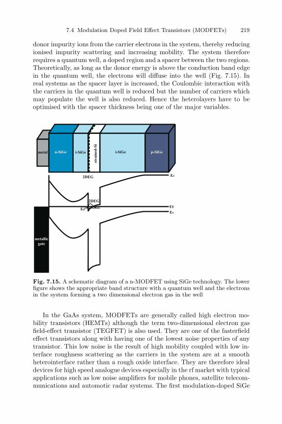
7.4 Modulation Doped Field Effect Transistors (MODFETs) 219
donor impurity ions from the carrier electrons in the system, thereby reducingionised impurity scattering and increasing mobility. The system thereforerequires a quantum well, a doped region and a spacer between the two regions.Theoretically, as long as the donor energy is above the conduction band edgein the quantum well, the electrons will diffuse into the well (Fig. 7.15). Inreal systems as the spacer layer is increased, the Coulombic interaction withthe carriers in the quantum well is reduced but the number of carriers whichmay populate the well is also reduced. Hence the heterolayers have to beoptimised with the spacer thickness being one of the major variables.
Fig. 7.15. A schematic diagram of a n-MODFET using SiGe technology. The lowerfigure shows the appropriate band structure with a quantum well and the electronsin the system forming a two dimensional electron gas in the well
In the GaAs system, MODFETs are generally called high electron mo-bility transistors (HEMTs) although the term two-dimensional electron gasfield-effect transistor (TEGFET) is also used. They are one of the fasterfieldeffect transistors along with having one of the lowest noise properties of anytransistor. This low noise is the result of high mobility coupled with low in-terface roughness scattering as the carriers in the system are at a smoothheterointerface rather than a rough oxide interface. They are therefore idealdevices for high speed analogue devices especially in the rf market with typicalapplications such as low noise amplifiers for mobile phones, satellite telecom-munications and automotic radar systems. The first modulation-doped SiGe

220 7. Hetero Field Effect Transistors (HFETs)
material was grown by John Bean and co-workers at Bell Laboratories in 1982while the first n-type devices was grown by Erich Kasper and co-workers atDaimler-Benz in 1986.
MODFETs are generally depletion mode devices. This is fine for discretedevices such as those found in the front ends of rf systems since the powerconsumed can be easily dissipated. For high integrtation densities, however,they consume much higher powers than enhancement mode devices mainlythrough the leakage currents between Ohmic contacts being enhanced bythe donor (or acceptor) doping layer in the channel and gate leakage sinceSchottky barriers are normally used rather than oxide gates. The integrationdensities of MODFETs are therefore limited compared to enhancement modeFETs. It is possible to design MODFET devices which work in enhancementmode but again leakage and power levels are still greater than comparablefully enhancement mode devices.
7.4.1 Low Temperature Propertiesof Two Dimensional Modulation-Doped Electronand Hole Gases
While the low temperature properties of modulation doped material are notthat useful for building circuits, by going to low temperatures the phononscattering in the system which typically dominates the room temperatureproperties can be removed, thereby allowing extraction of other scatteringmechanisms in the system. In particular this allows the roughness of het-erointerfaces and the background impurity concentrations in the material tobe minimised. In addition, by sweeping a magnetic field, Schubnikov de Haasoscillations can be found in the longitudinal resistivity (ρxx) and quantumHall platuea in the transverse resistivity (ρxy) as Landau levels formed inthe system and swept through the chemical potential. The temperature de-pendence of the Shubnikov de Haas oscillations also allows the extract ofthe effective mass of the electrons or holes in the modulation doped sample.Figure 7.16 shows the longitudinal and transverse magnetoresistivity from amodulation doped strained-Si quantum well grown on a relaxed Si0.77Ge0.23
virtual substrate grown by DERA and measured at Cambridge. The mobilityis 361 000 cm2/Vs with a carrier density of 3.4 ×1011 cm−2 at 55mK. Thissample also shows a number of fractional quantum Hall plateau in the trans-verse resistivity which demonstrate that the material is of extremely highquality. When Landau levels are split, high quality 2DEGs in silicon will alsohave spin and valley degeneracies split by the application of a magnetic fieldwhich can be resolved in Fig. 7.17. At lower magnetic fields these splittingswhich are weaker than the Landau level splittings will disappear.
To optimise the low temperature mobility when modulation doping is be-ing used, the spacer thickness must be carefully chosen. Larger spacers reducethe remote ionised impurity scattering since the electrons are taken furtheraway from the donors which created them, thereby reducing the Coulomb

7.4 Modulation Doped Field Effect Transistors (MODFETs) 221
0
200
400
600
800
1000
1200
1400
0
5000
10000
15000
20000
25000
30000
0 2 4 6 8 10 12 14 16
ρ xx (
Ω) ρ
xy (Ω)
B (T)
υ = 1
υ = 4/3
υ = 2
υ = 3
υ = 4
υ = 8/5
Fig. 7.16. The magnetoresistivity of a modulation doped Si/SiGe 2DEG grown byDERA with a mobility of 361 000 cm2/Vs and a carrier density of 3.4 ×1011 cm−2
at 55mK. The major integer and fractional quantum Hall plateau in the transversemagnetoresistance are shown
0
20
40
60
80
100
120
140
0 0.5 1 1.5 2
ρ xx (
Ω/
)
B (T)
55 mK
Fig. 7.17. An expanded version of the longitudinal resistivity of the 2DEG shownin Figure 7.16 showing both spin and valley splitting of the Landau levels

222 7. Hetero Field Effect Transistors (HFETs)
scattering. If the spacer is too thick then the carriers cannot get into thequantum well and both the carrier density and mobility in the quantum welltypically falls. Figure 7.18 shows a plot of carrier density against mobilityfor samples produced by a number of different groups, all at temperaturesof 4.2K or below. In addition to the experimental results, two theoreticalcurves produced by Frank Stern and Steven Laux at IBM have been drawn.These calculate the mobility as a function of carrier density for two differentbackground impurity density. The carrier density has been varied by varyingthe spacer in the modulation doped structure. It can be observed that lowerbackground impurity densities result in higher mobilities for a given carrierdensity and that lower carrier densities give higher mobilities.
The maximum in mobility occurs between 3 and 5 ×1011 cm−2. At highercarrier densities, the mobility is prodominantly limited by remote ionisedimpurity scattering. Therefore either larger amounts of dopant in the supplylayer or a thin spacer is limiting the mobility. Below 3 ×1011 cm−2, the falloff in mobility is the result of a mixture of interface roughness scatteringand remote ionised impurity scattering. All the samples have Ge contents inthe virtual substrates of between 20 and 30%. For the higher Ge contents,the interface roughness is higher which will reduce the mobility while thesplitting of the valleys is also higher which should increase the mobility sincethe probability of electrons occupying the upper valleys is reduced. For lowcarrier densities, lower Ge contents in the virtual substrate are required forhigher mobilities. The optimum mobility is therefore a compromise betweenremote ionised impurity scattering, the splitting of the valleys, the interfaceroughness in the system and the background impurity density.
7.4.2 Pseudomorphic MODFETs
One of the limiting factors in performance of CMOS is the p-channel MOS-FET. The mobility and effective masses are about 2.5 times lower in thep-MOS than the n-channel and so the transistors in CMOS have to be scaledaccordingly to balance the circuits. Hence the ability to match the size andperformance of the p-channel device to that of the n-MOS would be of signif-icant benefit to CMOS circuit performance. The ideal way of achieving thiswould be to have a pseudomorphic Si1−xGex channel grown below the oxidewith a large mobility comparable to the electron mobility (Fig. 7.19). Thistype of heterostructure layer is very similar to that used in the HBT.
The first pseudomorphic channel modulation-doped devices were produceby John Bean and co-workers at Bell Laboratories in 1982. A significantnumber of publications have appeared in the field trying to attempt such aheterostructure MOSFET device. Two major problems have been encoun-tered in trying to realise a technology that may be integrated in a CMOSproduction line. The first is that to integrate strained layers into a CMOS line,the structures should be as close to compatible with conventional processingas possible unless the performance gain is so large that increased production

7.4 Modulation Doped Field Effect Transistors (MODFETs) 223
10000
100000
2 3 4 5 6 7 8 9 10
IBMDERAImperialDaimlerBell Labs
Mob
ility
(cm
2/V
s)
Carrier density (x10 11 cm -2 )
20
500000
NB=10 14 cm -3
NB=10 15 cm -3
400000
300000
200000
5000040000
30000
20000
Fig. 7.18. The mobility below 4.2 K against carrier densities for modulation dopedSi/SiGe 2DEG grown by a number of different groups. The maximum in mobilityoccurs for carrier densities between 3 and 5 ×1011 cm−2. At higher carrier densities,the mobility is prodominantly limited by remote ionised impurity scattering. At lowcarrier densities, interface roughness scattering becomes prevalent
n-Si
(100)
2DHG
gatepoly
SiO2i-Sii-Sibuffer
p-Si i-Si
EF
Ev
parallel path
i-Si1-xGexgraded
Fig. 7.19. A buried channel-SiGe MOSFET demonstrating where parallel conduc-tion at the Si/SiO2 interface can occur

224 7. Hetero Field Effect Transistors (HFETs)
costs can be justified. Any strained layer incorporated must be below theequilibrium or Matthews and Blakeslee critical thickness otherwise disloca-tions and defects will result either from growth or during process anneallingstages reducing performance and yield. The high thermal budgets used inpresent CMOS production are not ideal for strained layers and may causestrain relaxation or diffusion. The second problem is that the valence banddiscontinuity of Si1−xGex to Si is small especially at low Ge contents andwith the Ge content being kept low to allow the Si1−xGex layer to be stableto thermal treatments, parallel conduction can occur in the transistors pro-ducing a 2D hole gas (2DHG) at the Si/SiO2 interface and the Si/Si1−xGex
interface (Fig. 7.19). The parallel conduction significantly reduces the per-formance of such devices. Finally, while such devices may have lower noisesince the holes are situated at a heterointerface with a higher mobility, thetransconductance will be lower than a comparable p-MOSFET or strained-Sip-MOSFET since the holes have been moved further away from the gate.
IBM demonstrated a modulation-doped heterostructure Si1−xGex MOS-FET which was processed using a CMOS fabrication process but performancewas only 20% or so better than a conventional p-MOS transistor. It is cheaperto down scale the p-MOS gate-length than to incorporate a technology withepitaxy into a production line with such performance and so a number ofcompanies have stopped research in this area. The best mobility achievedwas about 220 cm2/Vs in the Si1−xGex p-MOS at 300K and a value closerto 500 cm2/Vs is probably required before the technology can compete oneconomic grounds.
Better mobilities have appeared for pseudomorphic Si1−xGex channelMODFETs but many of these have parallel conduction or multiple subbandsat 300K and the true mobilities will be substantially different from the valuesquoted. As the gate-lengths in CMOS decrease, the thermal budgets also haveto decrease to prevent diffusion especially of dopants (Ohmic contacts andthreshold implants). A point may be reached where the extra confinementawarded by such a heterostructure transistor may be beneficial at small gate-lengths and the economics and reduced thermal budgets could then allow thetechnology to be implemented. The reason behind the relatively low mobil-ities in such structures are still not fully understood. Theoretical modellingsuggests that higher mobilites should be realised at room temperature butthese have not come to fruition in experiments. Even the low temperaturemobilities are much lower than predicted with values up to 17 000 cm2/Vsin the metallic regime at 300mK. Alloy scattering looks the most promisingexplanation as the theories used are by nature very simplified and may under-estimate the scattering but interface roughness and charge scattering alongwith other mechanisms cannot be completely overlooked. Ge clustering hasbeen observed in experiments and this may modify scattering processes, es-pecially alloy scattering, from the theories which assume a uniformly randomGe distribution.

7.4 Modulation Doped Field Effect Transistors (MODFETs) 225
7.4.3 Virtual Substrate MODFETs
From a performance view point, some of the most exciting Si1−xGex FET re-sults to date have been achieved with modulation doped field effect transistors(MODFETs) grown on virtual substrates. There are many different types ofheterolayer design for MODFETs as shown in Fig. 7.20. The standard designused is a direct copy of most GaAs / AlGaAs HEMT designs with the dopingabove the quantum well and a metal Schottky gate is used (Fig. 7.20(a)).Schottky gating in Si technology is far poorer than oxide gates due to muchhigher leakage currents. This leakage may be reduced by placing the dopingbelow the quantum well but it still remains orders of magnitude above anoxide gate (Fig. 7.20(b)). This design also has the advantage of reducing thechannel to gate distance and thereby increasing the transconductance of thedevice. The disadvantage is that surface segregation of the dopant or memoryeffects during growth can either make doping under the channel impossible orvery difficult. The carrier density may be increased, thereby maximising theconductance of the MODFET by placing doping on both sides of the quan-tum well (Fig. 7.20(c)). This has particular applications in a number of highpower analogue applications. Finally all of the above designs may also havea gate oxide incorporated to reduce the gate leakage current (Fig. 7.20(d)).
For all the designs discussed above an equivalent p-MODFET design alsoexists (Fig. 7.21). Basically a high Ge content layer will give a quantum wellin the valence band. The major consideration of the design of the structureis the quality of the strain relaxation buffer. While a pure Ge channel willhave no alloy scattering (or at least only a tiny amount from the leakage ofthe wavefunction of the holes into the SiGe spacer) and therefore on paperappear the best for performance. Pure Ge channels require a high Ge contentin the strain relaxation buffer, typically Si0.4Ge0.6 is required for a sensiblequantum well thickness, then the surface roughness of the buffer can be quitesevere and limit the performance. Khalid Ismail and colleagues at IBM hasused Si0.3Ge0.7 quantum wells on Si0.7Ge0.3 strained relaxation buffers whichare also the typical content used for the n-MODFET devices. This substan-tially reduces the surface roughness allowing short gate length transistors tobe easily fabricated along with potentially allowing the p-MODFETs to be in-tegrated with the n-MODFETs for complementary MODFET architectures.
7.4.4 Analytical Description of MODFET Operation
The operation of the MODFET is similar to that of the MOSFET as de-scribed in Sect. 5.3.2. Here we will describe the model of Drummond et al.which was originally designed for GaAs / AlGaAs MODFETs but is equallyapplicable to SiGe MODFETs. The reader should consider that in this orig-inal paper the energy terms had voltage units which was changed in thispaper. This will allow the important operating parameters of a MODFET to

226 7. Hetero Field Effect Transistors (HFETs)
i-Si
metal gate
i-Si cap
i-Si0.7Ge0.3
n-Si0.7Ge0.3
i-Si
SiGevirtual
substrate
p-Si substrate
2DEG
metal gate
i-Si cap
i-Si0.7Ge0.3n-Si0.7Ge0.3
SiGevirtual
substrate
p-Si substrate
(a) Normal n-MODFET (b) Inverted n-MODFET
metal gate
i-Si cap
i-Si0.7Ge0.3
n-Si0.7Ge0.3
i-Si
SiGevirtual
substrate
p-Si substrate
i-Si0.7Ge0.3n-Si0.7Ge0.3
2DEG
(c) High Density n-MODFET (d) Oxide Gated n-MODFET
metal / poly-Si
i-Si cap
i-Si0.7Ge0.3
n-Si0.7Ge0.3
i-Si
SiGevirtual
substrate
p-Si substrate
2DEG
oxide
2DEG
i-Si0.7Ge0.3
i-Si0.7Ge0.3
Fig. 7.20. Different designs for SiGe n-MODFETs. (a) Standard n-MODFET (b)the inverted MODFET with the doping under the channel (c) doping on both sidesof the channel to increase the carrier density and (d) an oxide gated device
metal gate
i-Si cap
i-Si0.7Ge0.3
p-Si0.7Ge0.3
i-Si0.3Ge0.7
SiGevirtual
substrate
n-Si substrate
2DHG
(a) SiGe channel p-MODFET (b) Ge channel p-MODFET
i-Si0.7Ge0.3
metal gate
i-Si cap
i-Si0.4Ge0.6
p-Si0.4Ge0.6
i-Ge
SiGevirtual
substrate
n-Si substrate
2DHG
i-Si0.4Ge0.6
Fig. 7.21. Schematic diagrams of SiGe p-MODFETs with (a) a SiGe channel and(b) a pure Ge channel

7.4 Modulation Doped Field Effect Transistors (MODFETs) 227
be described in terms of the sheet charge density in the 2DEG as a functionof mobility and carrier velocity. We will derived all the equations for electronsin an n-MODFET but these can easily be modified to those required for holesin a p-MODFET.
D r r
dd idcE
FE1E
0EFiE
FbE
b
FE
CE
d
doped supply
layer undopedspacer
quantum
well
undoped
substrate
gateN W
barrier
Fig. 7.22. A schematic diagram of the layered structure and conduction band withall the parameters required to model the properties of a MODFET
To start we impose the constraint that the amount of charge depleted fromthe donor supply layer must equal the charge accumulated at the heteroin-terface while the Fermi level is kept constant. The electron charge depletedfrom the donor supply layer is given by
ns =√
2εrε0
q2(∆Ec − EFb − EFi)ND + N2
Dd2i − NDdi (7.6)
where EFb is the separation between the conduction band in the barrier layerand the Fermi level, ND is the doping density in the donor supply layer,∆Ec is the conduction band discontinuity between the quantum well and thebarrier, εr is the dielectric constant of the barrier material, EFi is the Fermilevel with respect to the conduction band edge in the quantum well and di
is the thickness of the undoped spacer between the quantum well and thedoped supply layer. The electron charge stored at the heterointerface in thequantum well is given by
ns =
∞∫Ez,0
g2D (E) f (E)dE (7.7)

228 7. Hetero Field Effect Transistors (HFETs)
ns = g2D(E)kBT
ln[(
1 + exp
EFi − E0
kBT
)(1 + exp
EFi − E1
kBT
)](7.8)
where E0 and E1 are the lowest two subbands in the triangular quantumwell as calculated in Sect. 3.1.3. It is assumed here that only the lowestenergy states are filled or partly filled. More subbands can be used but itsubstantially complicates the problem and does not substantially improvesthe accuracy of the result. The 2D density of states is as given in (3.91). Theapplication of a voltage to the surface gate will deplete some or all of thecharge at the heterointerface in the quantum well. Simultaneously solving(7.6) and (7.8) with a known sheet carrier density allows the Fermi level tobe found in the system. Alternatively the sheet charge density can be foundif the Fermi level is known. With the addition of a gate bias with respect tothe source, Vg, the additional condition 7.9 fixes ns to
ns =εrε0
qd
[Vg − 1
q
(φb − q2NDd2
d
2εrε0+ EFi − ∆Ec
)](7.9)
where φb is the Schottky barrier height of the gate metal. d is the totaldistance between the gate and the 2DEG channel. Simultaneous solutions of(7.6) and (7.9) allow the carrier density in the 2DEG as a function of gatebias to be determined. (7.9) can be rewritten in the form
ns =εrε0
q (d + ∆d)[Vg − VT ] (7.10)
where the threshold voltage is defined as
qVT = φb − ∆Ec − q2NDd2d
2εrε0+ ∆E (T ) (7.11)
and where ∆E (T ) is a term for the temperature dependence of the systemwith ∆d related to the linearity of the carrier density to EFi such that
EFi = ∆E (T ) +q2∆d
εrε0ns (7.12)
These terms are determined from experiment and basically represent thedeviations between experimental values and the model.
Let us now add a drain bias to the system between the source and drainof the FET. In the long channel limit or for small source-drain biases, thevariation in the bias along the 2DEG channel can be added to the gate biasdescribing a channel potential V (x) to produce
ns =εrε0
q (d + ∆d)[Vg − VT − V (x)] (7.13)
For small values of V (x) it can be assumed that the mobility, µ, is constantalong the channel and so for a transistor of gate width, W it is found thatthe source drain current is

7.4 Modulation Doped Field Effect Transistors (MODFETs) 229
Ids = qµnnsWdV (x)
dx(7.14)
Ids = µnWεrε0
(d + ∆d)[Vg − VT − V (x)]
dV (x)dx
(7.15)
By integrating between the source and drain for a constant drain currentthe source drain current for a gate of length Lg is given by
Ids = µnWεrε0
(d + ∆d)Lg
(Vg − VT ) Vds − V 2
ds
2
(7.16)
To obtain the saturation source-drain current, we will use firstly the two-piece model which represent an abrupt transition from the constant mobilityregime to a velocity saturated regime. When the velocity of the electronsreaches saturation with a value, vsat = F
µn, the saturation current is given by
Ids,sat = µnWεrε0
(d + ∆d)Lg
[(Vg − VT )Vds,sat − V 2
ds,sat
2
]1 + (µnVds,sat/vsatLg)
(7.17)
A more accurate method is to use a smooth transition between the constantmobility and the velocity saturated regime. The Si velocity field curve satu-rates at about 6 ×10⁶ V/m and can be described by the expression
v =µF (x)
1 + µF (x)/vsat
(7.18)
where F (x) is the electric field in the channel which is equal todV (x)dx . The field
is not constant in the channel, however. Therefore the source-drain current
Ids = Wεrε0
(d + ∆d)(Vg − VT − V (x)) v (x)
=[µn
dV (x)dx
] [1 +
µdV (x)dx
vsat
]−1Wεrε0d + ∆d
(Vg − VT − V (x)) (7.19)
where vsat = µFsat with Fsat the electric field at which the velocity saturates.By integrating (7.19) from the source to the drain while remembering thatthe drain current must be constant, one obtains
Ids =µnW εrε0
(d+∆d)
(Vg − VT ) Vds − 1
2V 2ds
Lg + µn
vsatVds
(7.20)
It should be noted that if the saturation velocity approaches infinity, (7.20)reduces to (7.16) which is the long channel case. By using (7.19) and (7.20),the saturation source-drain current can be found as

230 7. Hetero Field Effect Transistors (HFETs)
Ids,sat =2 (Vg − VT )2 µnW εrε0
Lg(d+∆d)1 +
√[1 + 2µn(Vg−VT )
vsatLg
]2 (7.21)
We can now find the transconductance in the saturation regime as
gm,sat =dIds,sat
dVg|Vds=cons tan t
=(Vg − VT )µnW εrε0
Lg(d+∆d)1 + 2µn(Vg−VT )
vsatLg
√[1 + 2µn(Vg−VT )
vsatLg
] (7.22)
The maximum transconductance is obtained when the sheet charge densityis completely undepleted under the gate which produces
gm,max =qµnWns
Lg
[1 +
(qµns (d + ∆d)
εrε0vsatLg
)2]−1/2
(7.23)
For short gate lengths which represents almost all present day MODFETs,(7.23) reduces to
gm,max =vsatWεrε0
(d + ∆d)(7.24)
The transconductance from experimental measurements or the extrinsictransconductance is actually smaller than the intrinsic value given by (7.24)as the source resistance, Rs reduces the transconductance through negativefeedback. The equivalent circuit for a MODFET is shown in Fig. 7.23 wherethe resistances, capacitances and inductances which determine the high fre-quency behaviour of a MODFET are shown.
Ri
gmvcgs
Cdg
Cgs
gate
CdsGd
Rs
drain
source
Lg Lgd
Rg Rd
Ls
gm=gm0e-iωτ
Fig. 7.23. The equivalent circuit model that is commonly used for the analysis ofMODFETs and extraction of the important parameters

7.4 Modulation Doped Field Effect Transistors (MODFETs) 231
Therefore the extrinsic transconductance is
gm,max |ext =gm,max
1 + Rsgm,max
(7.25)
The current gain cutoff frequency, defined as the frequency at which thecurrent gain equals unity, since determined to be
fT =gm
2πCgs(7.26)
where Cgs is the gate-source capacitance since the feedback capacitance isnegligible compared to the input capacitance. It is clear from (7.26) that thehigher the saturation velocity and the smaller the gatelength, the higher fT .The maximum oscillation frequency, defined as the frequency at which thepower gain equals unity is given by
fmax =fT
2√
(Rg + Ri + Rs)Gd + 2πfT RgCdg
(7.27)
where the resistances and capacitances are those defined by the equivalentcircuit model in Fig. 7.23.
From all the equations above, it is clear that to optimise the performanceof MODFETs in circuits, either the saturation velocity must be increasedor the gatelength of the transistor must be decreased. As the former is afixed material parameter, it is the reduction of gatelength which primarilydetermines the transconductance and high speed performance. In addition,reduction of parasitic resistances and capacitances will increase the fmax ofa transistor. These are the reasons that the gatelength of MODFETs in allmaterial technologies is agressively scaled to lower gatelengths.
7.4.5 SiGe MODFET Performance
As a comparison of performance of both SiGe n and p-MODFETs, Fig. 7.24shows the cut-off frequency, fT as a function of gate-length for a numberof different transistor families. Care has been taken only to plot Si1−xGex
devices with fmax comparable or higher than fT . The lines correspond totheoretical scaling of the device geometry and for small gate-lengths the ex-perimental points lie below these curves due to increased parasitics. TheSi1−xGex n-MODFET has switching times comparable to n-MODFETs inGaAs/AlGaAs devices and larger than GaAs MESFETs. The Si1−xGex p-MODFET is even more impressive as the results are faster than any otherp-channel transistors published. Mobilities at 300K (77 K) of 2 830 cm2/Vs(18 000 cm2/Vs) at 2 × 1012 cm−2 (8 × 1011 cm−2) for the n-MODFET and1 300 cm2/Vs (14 000 cm2/Vs) at 1.5 × 1012 cm−2 (1.0 × 1012 cm−2) for thep-MODFET have been demonstrated. Transconductances in the n-type fora 0.25µm gate-length device at 300K (77K) was 330mS/mm (600mS/mm)and for a 0.1 µm p-MODFET 237mS/mm. At low temperatures the results

232 7. Hetero Field Effect Transistors (HFETs)
are more impressive with two dimensional electron gas (2DEG) mobilites upto 390 000 cm2/Vs at 400mK and two dimensional hole gases (2DHGs) reach-ing 55 000 cm2/Vs at 4.2K. The n-channel enhancements are due to reducedintervalley scattering with the strain splitting the valley degeneracy and thehigher saturation velocity achievable at lower electric fields (Fig. 3.32). The p-channel enhancements result from the lower effective mass and Ge-like strainmodified valance band structure. Initial modelling of circuit performance isalso encouraging. n-MODFETs with loads of 200 fF were shown to exhibit560 ps delays in NOR gates at 1.1V compared to 1400ps delays for the equiv-alent CMOS. The CMOS had to be run at 3.3V to achieve the same delay,consuming nine times the power of the Si1−xGex MODFETs. The possibil-ity of high-speed complementary logic with such devices looks promising onpaper.
10
100
0.1 1
Cut
-off
fre
quen
cy, f
T (
GH
z)
Gate length (µm)
20
30
4050
54
3
200
0.2 0.3 0.4 0.5 2
Si n-MOS
SiGe n-MODFET
GaAsMODFET
SiGe p-MODFET
GaAs MESFET
Fig. 7.24. The cut-off frequency, fT as a function of the gatelength of transistors forn-MOSFETs, strained-SiGe p-MODFETs grown on virtual substrates, strained-Sin-MODFETs, GaAs n-MESFETs and GaAs n-MODFETs
7.5 Further Reading
1. M.J. Kelly, Low Dimensional Semiconductors: Materials, Physics, Tech-nology, Devices” OUP, Oxford (1995)
2. J.H. Davies, The Physics of Low Dimensional Semiconductors, CUP,Cambridge (1998)

7.5 Further Reading 233
3. S.M. Sze, Semiconductor Devices: Physics and Technology, 2nd Edition,John Wiley and Sons, New York (2002)
4. L.D. Nguyen, L.E. Larson and U.K. Mishra, Proc. IEEE, 80, 494 (1992)5. D.J. Paul, Semiconductor Science and Technology 19, R59 (2004)6. L. Risch, Silicon Nanoelectronics: the next 20 years, in Silicon: Evolu-
tion and Future of a Technology, (P. Siffert, E. Krimmel, eds.), Springer,Berlin (2004)
7. T.J. Drummond, H. Morkoc, K. Lee, M. Shur, IEEE-EDL 3, 311 (1982)8. H. Heinrich, Modulation-Doped Filed-Effect Transistors, IEEE Press,
New York (1991)9. E. Kasper, S. Heim, Appl. Surf. Sci 224, 3 (2004)
10. N. Arora, MOSFET models for VLSI circuit simulation, Springer-Verlag,Wien (1993)
11. S. Karmalkar and G. Ramesh, IEEE-ED 47, 11 (2002)

8. Tunneling Phenomena
8.1 Tunnel Diodes
One of the true quantum devices which has no classical analogue is the tunneldiode where the quantum mechanical tunnelling of electrons or holes is usedto produce a negative differential resistance (NDR) region in the current-voltage characteristics. This NDR region allows the design of a number ofcircuits for applications including logic and memory. Tunnel diodes come intwo flavours, the intra-band resonant tunnelling diode (RTD) and the inter-band tunnel diode normally termed an Esaki diode. Esaki diodes have beenaround since the 1960s while the first RTD was produced in GaAs by LeoEsaki and Daniel Tsu in 1974. In the III-V system, RTDs are now a maturetechnology with many logic and memory circuits demonstrated along withthe fastest operation of any transit time device of 712GHz. In the siliconsystem, however, the band structure is not ideal for producing RTDs. Thefirst SiGe RTD was produced by Liu in 1988 and the first room temperatureoperation with extremely limited performance was in 1991. Since 1998, anumber of major breakthroughs have been achieved in both the inter-bandand the intra-band tunnel diodes which are now good enough to be able todemonstrate circuits at room temperature.
8.2 Resonant Tunnelling
Section 3.1 has shown the subband states in a quantum well along withtunnelling through a single barrier, and so the next system of interest isa double barrier system commonly known as a resonant tunnelling diodeor RTD. The basic system for calculating the transmission coefficient formultiple barriers and specifically a double barrier system is shown in Sect.8.2.1. The simplest way to calculate the transmission coefficient for the systemis to consider an electron in the central quantum well which may escape to theleft or the right (Fig. 8.1). The qualitative ideas behind resonant tunnellingwill be described in detail which should allow a detailed description of thephysics without complicated mathematical rigor. The operation of a RTD inmany ways is similar to a Fabry-Perot resonator in optics.

236 8. Tunneling Phenomena
left contact right contactwell
barrier barrier
E
0a2
a2
TL
TR
z
(a) (b)
~ ~
Fig. 8.1. (a) The wavefunction of an electron in the first bound state subband of aquantum well. (b) The same quantum well but with two barriers of finite thicknesson each side where the bound state becomes a resonance or quasi-bound
Figure 8.2 shows a schematic of the energy band structure of a RTD with aquantum well between two barriers in the conduction band of a semiconductorheterostructure system such as Si / SiGe. On the right is shown the idealtransmission coefficient for electrons incident on the barriers with energyE which is derived below in Sect. 8.2.1. The transmission coefficient peaksevery time an electron with energy equal to one of the subband energies inthe quantum well is incident on the barriers. The current through the systemtherefore peaks every time the electrons can tunnel into an allowed subbandstate - basically the subband is a resonant state - hence the name resonanttunnelling diode.
The detailed current voltage properties of a RTD may be derived fromthe transmission properties and the band structure of the material. Let usdefine the transmission and reflection coefficients through the right barrieras TR and RR respectively and those through the left barrier as TL and RL
(Fig. 8.1).
8.2.1 T -Matrices
Here the idea of T -matrices will be introduced. More detailed derivations canbe found in the references at the end of the chapter. The great advantage ofT -matrices is that once the transmission and reflection coefficients are knownfor a number of barriers, then the transmission through any combination ofthe barriers may be calculated using matrix algebra. For double or triplebarrier systems, this is far easier to calculate than the complex integralsfrom more common techniques.
8.2.2 The Single Barrier
Let us generalise the tunnelling problem to any barrier where the incidentwavefunction has amplitude A with wavevector k1, the reflected wavefunc-

8.2 Resonant Tunnelling 237
Energy
Transmission Coefficient
Ec
Incident
Reflected
Transmitted
1 10-2 10-4 10-6 10-8 10-10
E0
E1
E2
E3
Γ
Fig. 8.2. A schematic diagram of the energy band structure of a RTD with anumber of subbands in the quantum well defined between two barriers of e.g. SiGe.The diagram on the right shows the transmission coefficient with energy and theresonances which occur as the energy of an incident electron coincides with each ofthe energies of the subbands in the quantum well
A exp (ik1z)
B exp (-ik1z)
C exp (ik2z)
D exp (-ik2z)
barrier
region 1 region 2
E
Fig. 8.3. A schematic showing a general transmission problem with a barrier ofarbitrary height and shape. Each side of the barrier may have incoming and outgoingwaves and the wavevectors on each side of the barriers may be different
tion has amplitude B and wavevector k1, the transmitted wavefunction hasamplitude C and wavefunction k2 and a final incident wavefunction to thebarrier from the right with amplitude D and wavefunction k2 is also includedto represent any reflections from anything to the right of the barrier (Fig.8.3). Let us define the transmission coefficient for tunnelling from region 1 toregion 2 as T (21) such that(
CD
)= T (21)
(AB
)=(
T(21)
11 T(21)
12
T(21)
21 T(21)
22
)(AB
)(8.1)

238 8. Tunneling Phenomena
A exp (ik1z)
B exp (-ik1z)
C exp (ik2z)
D exp (-ik2z)
barrier
region 1 region 2
E
E exp (ik3z)
F exp (-ik3z)
region 3
barrier
Fig. 8.4. A schematic diagram of a double barrier system
Expanding this to the two barriers of Fig. 8.4 such that(CD
)= T (21)
(AB
) (EF
)= T (32)
(CD
)(8.2)
which when combined produces(EF
)= T (32)T (21)
(AB
)≡ T (31)
(AB
)(8.3)
The order of the superscripts should now be clear as T (31) = T (32)T (21).Therefore as long as one may define the T matrices for all the barriers in asystem, these may be multiplied together to find the total transmission andreflection in the system. The matrices must be written in the opposite orderto the numbering of the barriers from left to right so that they act on theamplitudes of the waves in the correct sequence.To find the transmission andreflection coefficients, the waves on either side of a single barrier are relatedthrough(
t0
)= T
(1r
)=(
T11 T12
T21 T22
)(1r
)(8.4)
and so
r = − T21
T22
t =T11T22 − T12T21
T22
(8.5)
Using the conservation of current and time reversal invariance, it can be
shown that T22 = T ∗11, T21 = T ∗
12 and∣∣∣T11
∣∣∣2 −∣∣∣T12
∣∣∣2 = det∣∣∣T ∣∣∣ = 1. Hence
the previous equations may be simplified to
r = − T ∗12
T ∗11
t =1
T ∗11
(8.6)
Let us now re-examine the single barrier problem using the T -matrices.

8.2 Resonant Tunnelling 239
T (31) =
(e−
ik1b/2 00 e
ik1b/2
)T (k1, k2)
(eik2b/2 0
0 e−ik2b/2
)(8.7)
(eik2b/2 0
0 e−ik2b/2
)T (k2, k1)
(e−
ik1b/2 00 e
ik1b/2
)
The middle pair of matrices can be multiplied to produce a matrix withexp (±ik2b) on the diagonal, reflecting the change in phase while travellingbetween the barrier and the free space. Multiplying this out gives
T (31) =1
2k1k2
(e−
ik1b/2 00 e
ik1b/2
)(8.8)
×(
2k1k2 cos (k2b) + i(k21 + k2
2
)sin (k2b)
i(k21 − k2
2
)sin (k2b)
−i(k21 − k2
2
)sin (k2b)
2k1k2 cos (k2b) − i(k21 + k2
2
)sin (k2b)
)
×(
e−ik1b/2 00 e
ik1b/2
)
After completing the multiplication it is found that
T(31)21 =
i(k21 − k2
2
)sin (k2b)
2k1k2(8.9)
T(31)22 =
2k1k2 cos (k2b) − i(k21 + k2
2
)sin (k2b)
2k1k2exp [ik1b] (8.10)
To find the transmission coefficient we require to find the transmission am-plitude
t =T11T22 − T12T21
T22
= (8.11)
1T22
=2k1k2 exp [−ik1b]
2k1k2 cos (k2b) − i (k21 + k2
2) sin (k2b)
8.2.3 Double Barriers - The Resonant Tunnelling Diode
The next stage is to calculate the transmission coefficient for the doublebarrier system. The trick to make the algebra as simple as possible is todefine the origin at the centre of the well so the structure is symmetric aroundthe origin in the z-axis. In addition it is also easier to consider a trapped

240 8. Tunneling Phenomena
electron in the quantum well which can escape to the right with transmissionamplitude tR, relection amplitude rR and transmission coefficient TR or to theleft with transmission amplitude tL, relection amplitude rL and transmissioncoefficient TL (Fig. 8.1). The electron will travel to the right through the rightbarrier and to the left through the left barrier. The T-matix for an electronimpinging from the left is
TL =
( 1/t∗L
r/tL
r∗L/t∗L
1/tL
)(8.12)
Using the same technique as the single barrier, we now form the T (31) trans-mission coefficient for the double barrier
T =
(e−
ika/2 00 e
ika/2
)(1/
t∗R −r∗R/t∗R
−rR/tR
1/tR
)(8.13)
×(
eika/2 00 e−
ika/2
)(eika/2 00 e−
ika/2
)
×( 1/
t∗LrL/tL
r∗L/t∗L
1/tL
)(e−
ika/2 00 e
ika/2
)
=
( (1−r∗Lr∗
R exp(−2ika))
t∗L
t∗R
(rL exp(ika)−r∗R exp(−ika))
tL t∗R
(r∗L exp(−ika)−rR exp(ika))
t∗L
tR
(1−rLrR exp(2ika))
tL tR
)
The transmission amplitude follows from the bottom right entry
t =tLtR
1 − rLrR exp [2ika](8.14)
Rewriting the complex reflection amplitudes in the polar formrL = |rL| exp (iϑL) then
T =∣∣t∣∣2 =
TLTR
1 + RLRR − 2√
RLRR cos [2ka + ϑL + ϑR](8.15)
=TLTR(
1 −√
RLRR
)2
+ 4√
RLRR sin2(
φ2
)where the phase φ = 2ka + ϑL + ϑR. This is the transmission coefficient fora double barrier with distance a between the centres of the barriers.We areinterested in finding the variation of T with energy (i.e. T (E)) to allow thecurrent-voltage relationship to be found. If we assume that the most rapidlychanging part of the system will be the phase of the electron between thebarriers (i.e. 2ka) and all other variables change slowly with respect to this

8.2 Resonant Tunnelling 241
then T has peaks (Fig. 8.2) when the sine in the denominator vanishes i.e.φ = 2nπ. Therefore T has resonance peaks when
Tres =TLTR(
1 −√
RLRR
)2 ≈ 4TLTR(TL + TR
)2 (8.16)
It may be seen that if TL = TR i.e. both barriers have identical transmissioncoefficients then Tres = 1 i.e. perfect transmission. It can also be shown thatif the individual transmission coefficients are small then T may be approxi-
mated by T ≈ TLTR
14
(TL + TR
)2
+ 4 sin2(
12φ)
= Tres1
1 + 16
(TL+TR)2 sin2(
12φ) (8.17)
If we use the approximation sin2(
12φ) ≈ 1
2 then
T ≈ 12TLTR (8.18)
Thus the overall transmission when off-resonance is typically the productof the individual transmissions for the two barriers.Strong deviations maybe expect from this when the sin approaches zero. Therefore if we set φ =2nπ + δφ and expand the sin we find
T ≈ Tres1
1 + 4(δφ)2
(TL+TR)2
=Tres
1 +(
2δφφ0
)2 (8.19)
where φ0 = TL + TR. This shows a resonance peak with a Lorentzian shapewhich falls to half its peak value at δφ = φ0. Thus φ0 is the full width athalf-maximum (FWHM) value. To translate this into energy
Γ =dE
dk
dk
dφφ0 =
hv
2a
(TL + TR
)(8.20)
where v is the velocity of the electron between the barriers and it is assumedthat the phase is again dominated by 2ka.
The width Γ can also be derived from basic physical considerations. Weassume that an electron has managed to tunnel into a subband and is caughtbetween the two barriers for an amount of time, τ . The velocity of an electronin the resonant subband state is v and the distance of a round trip is 2a.Therefore the electron will hit the left barrier v/2a times per second (and theright barrier a similar number of times) if it does not escape. The probabilityof escaping is TL on each occassion which gives a mean escape rate throughthe left barrier of vTL/2a. To convert this into an energy uncertainty, theHeisenburg’s uncertainty principle tells us that this value must be multipliedby h. The total rate when the similar term for the right barrier is added gives
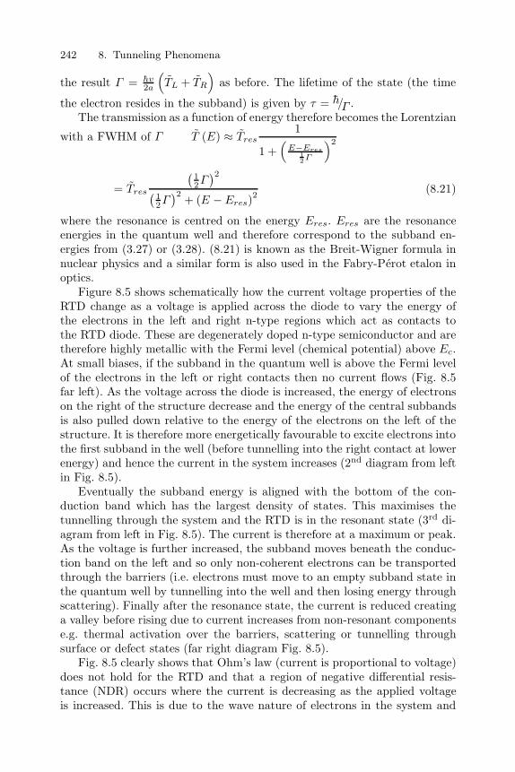
242 8. Tunneling Phenomena
the result Γ = hv2a
(TL + TR
)as before. The lifetime of the state (the time
the electron resides in the subband) is given by τ = h/Γ .The transmission as a function of energy therefore becomes the Lorentzian
with a FWHM of Γ T (E) ≈ Tres1
1 +(
E−Eres12 Γ
)2
= Tres
(12Γ)2(
12Γ)2 + (E − Eres)
2(8.21)
where the resonance is centred on the energy Eres. Eres are the resonanceenergies in the quantum well and therefore correspond to the subband en-ergies from (3.27) or (3.28). (8.21) is known as the Breit-Wigner formula innuclear physics and a similar form is also used in the Fabry-Perot etalon inoptics.
Figure 8.5 shows schematically how the current voltage properties of theRTD change as a voltage is applied across the diode to vary the energy ofthe electrons in the left and right n-type regions which act as contacts tothe RTD diode. These are degenerately doped n-type semiconductor and aretherefore highly metallic with the Fermi level (chemical potential) above Ec.At small biases, if the subband in the quantum well is above the Fermi levelof the electrons in the left or right contacts then no current flows (Fig. 8.5far left). As the voltage across the diode is increased, the energy of electronson the right of the structure decrease and the energy of the central subbandsis also pulled down relative to the energy of the electrons on the left of thestructure. It is therefore more energetically favourable to excite electrons intothe first subband in the well (before tunnelling into the right contact at lowerenergy) and hence the current in the system increases (2nd diagram from leftin Fig. 8.5).
Eventually the subband energy is aligned with the bottom of the con-duction band which has the largest density of states. This maximises thetunnelling through the system and the RTD is in the resonant state (3rd di-agram from left in Fig. 8.5). The current is therefore at a maximum or peak.As the voltage is further increased, the subband moves beneath the conduc-tion band on the left and so only non-coherent electrons can be transportedthrough the barriers (i.e. electrons must move to an empty subband state inthe quantum well by tunnelling into the well and then losing energy throughscattering). Finally after the resonance state, the current is reduced creatinga valley before rising due to current increases from non-resonant componentse.g. thermal activation over the barriers, scattering or tunnelling throughsurface or defect states (far right diagram Fig. 8.5).
Fig. 8.5 clearly shows that Ohm’s law (current is proportional to voltage)does not hold for the RTD and that a region of negative differential resis-tance (NDR) occurs where the current is decreasing as the applied voltageis increased. This is due to the wave nature of electrons in the system and

8.2 Resonant Tunnelling 243
I
V
eV
e
Vp
EFL
EFR
Ec
Ec
VT
Fig. 8.5. A schematic diagram showing the current-voltage properties of a RTDalong with the appropriate energy band diagrams for the electron transport. VT
is the threshold voltage for current transport and Vp is the voltage at which thecurrent peaks
the interaction with the quantised states produced from a low dimensionalsystem. It is this NDR which may be utilised in an amplifier or oscillator forcircuit applications.
The voltage at which the peak current is observed is Vp (Fig. 8.5). Anapproximate value for this may be estimated by considering a voltage Vacross the device. Since the voltage is dropped from the left contact to theright contact corresponding to energy difference between the left and rightchemical potentials of qV , half this voltage will be dropped between eachcontact and the quantum well. Therefore
qVp
2≈ Eres (8.22)
where Eres = E0 in (3.27) or (3.28).It is worth noting that this voltage is that which is dropped across the
tunnel barriers and the measured value may be substantially different due tothe finite resistance of the doped contact regions on either side of the wellsand any contact resistances.
Up to this point we have only calculated the transmission coefficient whilein experiments, the current is normally measured as a function of applied volt-age. The general method used to calculate the current considers electronsimpinging from the left and then adds the contribution due to electrons ar-riving from the right. The basic current equation is then related to the wellknown expression for current density of J = nqv where n is the density, q is

244 8. Tunneling Phenomena
the electron charge and v is the velocity of the electrons or holes. To find thetunnelling current density we again use electron velocity and the transmissioncoefficient
JL = q
∞∫0
g (E) f (E)vLT (E) dE (8.23)
with a similar expression for the right-hand side with the electrons movingin the opposite direction. The total current density is given by
J = JL − JR (8.24)
For the full result the left and right current densities must be integratedover x−, y− and z−directions but a number of approximations and simplifi-cations can be made.
kz
kx
ky
Fig. 8.6. The 3D Fermi sphere separating the filled from the unfilled states and a2D slice along kz which represents the quantised states in the quantum well
For the full three dimensional device it is worthwhile noting that whilethe leads on each side of the barriers are 3D, the quantum well has quantisedstates in the z-direction and hence the electrons are in a 2D layer. Thereforeelectrons tunnelling through the system start from 3D and tunnel through a2D system back to a 3D system. One can think of this as each lead havinga Fermi sphere which is sliced into a Fermi circle when the electrons tunnelinto a resonant state (see Fig. 8.6). The density of states in the integral istherefore 2D. Again if we assume that a large bias is applied to the device sowe may ignore the electrons in the right-hand contact then it may be shownthat
J =qm∗
2π2h3
µL∫EcL
(µL − E) T (E) dE
=qm∗
2π2h3 (EFL − Eres)π
2Γ Tres (8.25)

8.2 Resonant Tunnelling 245
8.2.4 The Resonant Tunnelling Diode (RTD)
Ec
AlAsbarriers
GaAs
relaxedSiGe
Ec
Ec
strained-SiGebarriers
strained-Si
relaxedSiGe
strained-Si
relaxedSiGe
barriers(a)
(b)
(c)
Fig. 8.7. A schematic diagram for the different band structures for RTDs withdifferent materials showing the band alignments without any charges in the devices.(a) The typical and ideal band structure in the III-V system where the barriers havea height of over 1 eV. (b) The early Si/SiGe RTD structure where quantum wellsare used to produce two barriers. (c) The use of strained barriers allows a muchhigher barrier than relaxed barriers greatly improving performance
The problems of producing a Si/SiGe RTD may be easily demonstratedwhen one considers the band structure typically used for high performanceIII-V RTDs. Figure 8.7(a) shows the typical GaAs/AlAs system where theAlAs layers provide a barrier to electrons which is over 1 eV high. The prob-lem with Si/SiGe is that it is very difficult to produce a significant barrier foreither electrons or holes. The typical method employs quantum wells (Fig.8.7(b)) where the barriers use the same material as the contacts. This pro-duces substantial problems since electrons may easily be excited over thebarriers especially at higher temperatures of operation, a problem which isknown as thermionic emission. The best performance of these types of deviceshas only just shown NDR at room temperature with a peak-to-valley current(PVCR) ratio of only 1.2. For use in circuits to be discussed in Sect. 8.2.6, aPVCR of at least 2 and preferably 3 or greater is required.
As an example of a typical III-V RTD, Fig. 8.8 shows the I-V for a n-GaAsRTD with 2 nm thick AlAs barriers and a 6 nm GaAs quantum well betweenthe barriers. Two almost symmetrical current peaks are shown close to 1 V inboth the positive and negative bias directions. The important figures of meritfor an RTD are the peak current density (Jp), the peak to valley current ratio(PVCR) and the peak voltage (Vp).
Figure 8.7(c) shows the technique demonstrated by Douglas Paul at Cam-bridge where the barriers in the RTD are compressively strained. From the

246 8. Tunneling Phenomena
-20
-10
0
10
20
-2 -1 0 1 2
Voltage (V)
Cur
rent
den
sity
(M
A/m
2 )
293 K
Fig. 8.8. The current density against bias voltage at 293 K for a n-GaAs RTD with2 nm thick AlAs barriers and a 6 nm GaAs quantum well between the barriers
Ec
relaxedSi0.8Ge0.2substrate
[001]
[100]
[010]
[001]
[100]
[010][001]
[100]
[010]
2DEG
E0
strained-Si0.6Ge0.4barriers
strained-Siquantum well
Fig. 8.9. A schematic diagram of the conduction band of a Si/SiGe RTD withstrained wells and barriers with the different splitting of the valleys shown
band structure diagrams in Sect. 4.5, by compressively straining the barri-ers, the conduction band mimima, ∆Ec, is raised producing a larger bar-rier to electron tunnelling. This greatly reduces the thermionic emission overthe tops of the barriers and produces significantly better performance athigher temperatures. Figure 8.9 shows the band structure of a typical RTD.Strained-Si quantum wells are placed at either side of the barriers which willhelp the barriers height through band bending when a bias is placed acrossthe device. These spacers also reduce the capacitance of the diode which will

8.2 Resonant Tunnelling 247
become important for the implementation into circuits. The strain in the bar-riers split the valleys so that the ∆4 valleys are the lowest in energy about110 meV above the substrate conduction band while the ∆2 valleys are raisedfurther and may be ignored. The strained-Si quantum wells only have the ∆2
valleys occupied.
Regrowth interface
2 nm barriers3 nm quantum well
Fig. 8.10. A transmission electron micrograph (TEM) of a Si/SiGe RTD with 2 nmthick Si0.4Ge0.6 barriers on a relaxed Si0.8Ge0.2 substrate
0
50
100
150
200
250
300
0 0.5 1 1.5 2 2.5 3
Voltage (V)
Cur
rent
den
sity
(kA
/cm
2 )
5 x 5 µm
7 x 7 µm
10 x 10 µm
Fig. 8.11. The current voltage characterisitics from three different sizes of Si/SiGeRTD with 2 nm thick Si0.4Ge0.6 barriers on a relaxed Si0.8Ge0.2 substrate. Thedevices have sizes of 5 × 5µm, 7 × 7 µm and 10 × 10µm

248 8. Tunneling Phenomena
The wafers for this work were grown by CVD. First a n-type thick virtualsubstrate with a Ge content up to Si0.8Ge0.2 was grown. The wafer wasthen removed from the growth chamber and given a modified RCA cleanto remove excess As from the surface in an attempt to circumvent the Asdopant segregation problems in CVD material. This can be seen as a whitelayer just below the lower strained-Si spacer as the RCA clean leaves a Si-rich layer at the interface in TEM pictures of the sample (Fig. 8.10). Thewafers were replaced in the growth chamber and the following layers grown:10 nm i-Si0.8Ge0.2 buffer, 10 nm i-Si spacer, 2 nm i-Si0.4Ge0.6 barrier, 3 nm i-Siwell, 2 nm i-Si0.6Ge0.4 barrier, 10 nm i-Si spacer, 50 nm n-Si0.7Ge0.3 doped atND ∼ 3 × 1018 cm−3 and a 4 nm n-Si cap. Figure 8.10 shows a TEM pictureof the active layers of one such RTD grown by CVD at DERA, Malvern.
0
5
10
15
20
0 0.05 0.1 0.15 0.2 0.25 0.3
7x7 µm
5x5 µm
Voltage (V)
Cur
rent
den
sity
(A
/cm
2 )
Jp = 14.9 A/cm
2
PVCR = 2.1
Fig. 8.12. A RTD grown by MBE with the structure modelled in Fig. 8.13. Threepeaks are clearly shown which correspond to the peaks in Fig. 8.13. The seriesresistances along with Ge segregation and diffusion result in the peaks from theexperiment not agreeing completely with the theory
The current voltage characteristics at 298K are shown in Fig. 8.11. Thepeak that is observed in the positive bias direction has a peak current densityof 282kA/cm2 for a PVCR of 2.4. A similar wafer with barriers of Si0.8Ge0.2
did not demonstrate any NDR at room temperature showing the additionalbenefits of the larger barrier heights with increase Ge content. The disad-vantage of this system is that with the present design, the peak voltage isvery high at about 2V. For applications this needs to be less than 1V. Thisis mainly due to the relatively small amount of n-type doping which CVD

8.2 Resonant Tunnelling 249
0.0 0.2 0.4 0.6 0.8 1.0
Vsd (V)
10-11
10-9
10-7
10-5
10-3
10-1
101
103
Cur
rent
Den
sity
(kA
/cm
2 )
total currentlocalised statesextended states
Et
1
El
1
El
2
Et
1
El
1 El
2
0.0 0.2 0.4 0.6 0.8 1.0-0.3
-0.2
-0.1
0.0
0.1E
(m
eV)
central well:
spacer well:
(a)
(b)
Fig. 8.13. The subband energy levels in the main quantum well and the emitter-spacer quantum well along with the current-voltage characterisitics calculated fromtheory for the RTD in Fig. 8.11. A subscript of l corresponds to the longitudinalmass and t to a transverse mass. The calculations are by Igor Zozoulenko
allows to be incorporated into the Ohmic contacts of less than 5× 1018 cm−3
which results in large contact resistances and therefore large peak voltages.Figure 8.12 shows the same design of RTD grown by solid source MBE. Herethe doping has been increased to 5 × 1019 cm−3 and the peak voltage hasbeen significantly reduced.
When the RTD is modelled (see Fig. 8.13), the tunnelling of electronsthrough the system is actually dominated by electrons from the bulk virtualsubstrate. The splitting of the valleys in the strained-Si spacer results in onlythe ∆2 valleys being populated. These have a low transverse effective massof 0.198me along the quantum well but have a high longintudinal effectivemass of about 0.98me in the vertical tunnelling direction. As was shown insection 3.1, the transmission coefficient for quantum mechanical tunnellingdepends exponentially on the square root of the effective mass,
T ≈ 16E
V0exp
⎛⎝−2
√2m∗ (V0 − E)
h2 b
⎞⎠ (8.26)
Therefore the heavy mass in the strained-Si spacer is unlikely to tunnel com-pared to the light mass from the bulk substrate with 6 valleys all degenerate.

250 8. Tunneling Phenomena
In addition, the selection rules in the system dictate that longitudinal effec-tive mass electrons can only tunnel to longitudinal electron states and thattransverse mass electrons can only tunnel to transverse mass electron statesunless the electron is scattered (typically by a phonon to change the momen-tum of the electron). When all this is put together and modelled (Fig. 8.13)the localised states in the strained-Si spacer quantum well play little part inthe observed I-V characteristics while the main NDR peaks are dominatedby the extended states from the bulk virtual substrate. The three main peaksin Fig. 8.12 can all be identified in the theory plot of Fig. 8.13 but the ab-solute values of current are not correct in the theory. The difference betweenthe experimental and theoretical voltages observed in Figs. 8.11 and 8.13 isbecause the theory does not take any account of series resistances in the cir-cuit such as contact resistances or the resistances of the doped regions oneither side of the barriers. Therefore a substantial amount of voltage can bedropped across these regions before any significant voltage is dropped acrossthe active barrier regions.
The high peak voltage can be understood from the charging in the system.Figure 8.14 shows self-consistent Poisson-Schrodinger solutions for the RTDwith voltages of 0.2 to 0.5V applied across the device region shown. It can beobserved that at low biases (0.2V) there is a substantial charge build up onthe right hand side of the second spacer. Basically this layer is the result of the∆Ec discontinuity between the strained-Si spacer and the relaxed Si0.8Ge0.2
virtual substrate at the collector end of the device. This charge layer screensthe applied potential from the barriers and therefore a larger potential mustbe applied to the totalsystem before the bands are brought sufficiently downthat subbands align and electrons can tunnel through the system. As theapplied voltage is increased to 0.2 and then 0.3V, the charge at the collectoris slowly reduced until by 0.5V, it has almost completely disappeared. Figure8.14 also shows the band bending in the strained-Si spacers which give thebarriers a larger height compared to a RTD without spacers on either sideof the barriers. One problem with the strained-Si spacers is that they allowcharge to be built up also at the emitter side which again provides problemsfor the fast operation of such diodes.
A method to stop the charge build up was suggested by Neil Griffin andBarry Coonan at NMRC in Ireland. Basically the spacers are graded so thatthere is no ∆Ec discontinuity across the emitter or collector contact endsof the device. Figure 8.15 shows self-consistent Poisson-Schrodinger solutionsfor the structure both at a bias of 0V (Fig. 8.15(a)) and 0.2V (Fig. 8.15(b)).The band structure looks very similar to that of a III-V RTD (see Fig. 8.7(a))when a bias is applied. More important is the charge density in the structurewhen a bias is applied as shown in Fig. 8.15(c). No charge is built up atthe emitter or collector contact and so the device should operate with muchsmaller applied voltages.
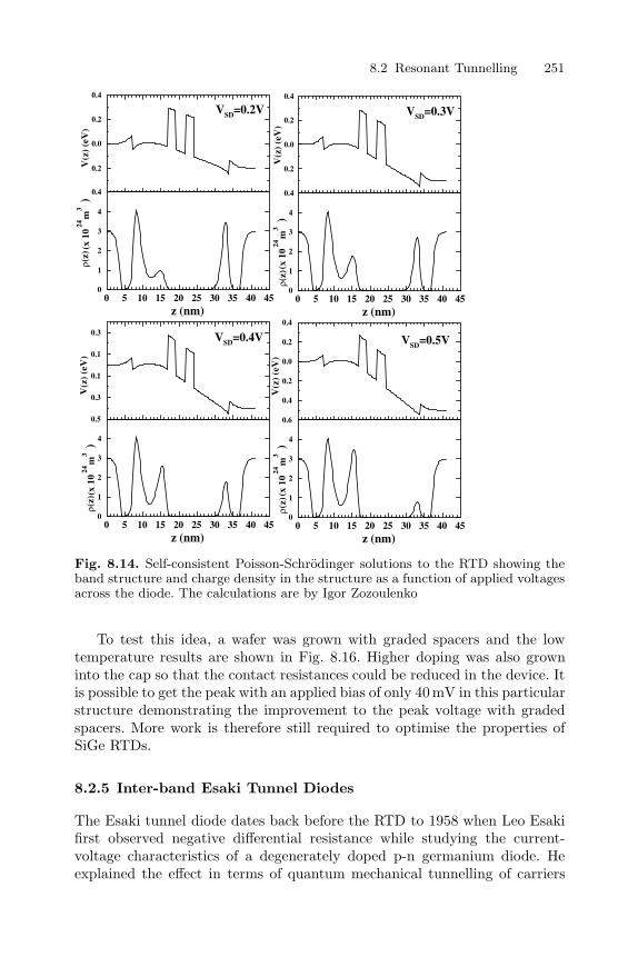
8.2 Resonant Tunnelling 251
0 5 10 15 20 25 30 35 40 45z (nm)
0
1
2
3
4
(x 1
024
m3
)
0.5
0.3
0.1
0.1
0.3
V(z
) (e
V)
0 5 10 15 20 25 30 35 40 45z (nm)
0
1
2
3
4
ρ(z)
(x 1
024
m3
)
0.4
0.2
0.0
0.2
0.4V
(z)
(eV
)
0 5 10 15 20 25 30 35 40 45z (nm)
0
1
2
3
4
(x 1
024
m3
)
0.4
0.2
0.0
0.2
0.4
V(z
) (e
V)
0 5 10 15 20 25 30 35 40 45z (nm)
0
1
2
3
4
(x 1
024
m3
)
0.6
0.4
0.2
0.0
0.2
0.4
V(z
) (e
V)
VSD=0.3VVSD=0.2V
VSD=0.4V VSD=0.5V
ρ(z)
ρ(z)
ρ(z)
Fig. 8.14. Self-consistent Poisson-Schrodinger solutions to the RTD showing theband structure and charge density in the structure as a function of applied voltagesacross the diode. The calculations are by Igor Zozoulenko
To test this idea, a wafer was grown with graded spacers and the lowtemperature results are shown in Fig. 8.16. Higher doping was also growninto the cap so that the contact resistances could be reduced in the device. Itis possible to get the peak with an applied bias of only 40mV in this particularstructure demonstrating the improvement to the peak voltage with gradedspacers. More work is therefore still required to optimise the properties ofSiGe RTDs.
8.2.5 Inter-band Esaki Tunnel Diodes
The Esaki tunnel diode dates back before the RTD to 1958 when Leo Esakifirst observed negative differential resistance while studying the current-voltage characteristics of a degenerately doped p-n germanium diode. Heexplained the effect in terms of quantum mechanical tunnelling of carriers

252 8. Tunneling Phenomena
distance z (nm)
-0.3
-0.2
-0.1
0.0
0.1
0.2
0.3
V(z
) (e
V)
0e+00
1e+24
2e+24
3e+24
4e+24
(z)
Vsd =0.2V
EF
=6.3meV
ρ
0 10 20 30 40
0 10 20 30 40
-0.2
-0.1
0.0
0.1
0.2
0.3
0.4V
(z)
(eV
)
Si
(a)
0 10 20 30 40
Vsd =0.2V
Vsd =0.0V
Si0.8Ge0.2 Si0.8Ge0.2
gradedSiGe
gradedSiGe
Si0.4Ge0.6barriers
(c)
(b)
Fig. 8.15. Self-consistent Poisson-Schrodinger solutions to a RTD with gradedspacer wells showing the band structure and charge density in the structure asa fucntion of applied voltages across the diode. The calculations are by Igor Zo-zoulenko
between the p and n-doped regions of the device.The tunnelling time forinterband tunnelling is proportional to exp [2k (0) b] where b is the barrierthickness and k (0) is the mean value of the momentum encountered in thetunnelling path corresponding to an incident carrier with zero transverse mo-mentum and energy equal to the Fermi energy. This tunnelling time is veryshort and allows operation of tunnel devices in the 30 to 300GHz regime.
The basic form of an Esaki diode is shown in Fig. 8.17. Two highly dopedregions, one n-type and the other p-type are placed together and a depletionregions forms between the two. The doping must be high enough for bothdoped regions to be degenerate. The amount of degeneracy for electrons, Ve
and holes Vh requires to be a few kBT to produces a large density of stateson both sides of the junctions. The depletion width is typically 10 nm or less,much narrower than many conventional p-n junctions. Therefore from Fig.5.2 the doping must be greater than 1019 cm−3 in the doped regions.

8.2 Resonant Tunnelling 253
-0.15
-0.10
-0.05
0.00
0.05
0.10
-0.1 -0.05 0 0.05 0.1 0.15
Cur
rent
Den
sity
(A
/cm
2)
Voltage (V)
77 K
Fig. 8.16. The current voltage characteristics of a RTD with graded spacers at77 K. The peak current has now shifted to 40mV showing the effect of grading thespacers in the device
Ec
Ev
np
p+-Si n+-Si
depletionregion
eVeVh eVe
Fig. 8.17. An Esaki tunnel diode with the energy band structure. Vh and Ve arethe degeneracies of the holes and electrons respectively

254 8. Tunneling Phenomena
The typical current-voltage characteristics are shown in Fig. 8.18. For theexplanation, it will be assumed that the n- and p-doped regions have thesame doping density. At zero applied bias at thermal equilibrium, the rate oftunnelling from the n- to the p- and from the p- to the n- are equal at a finitetemperature and no net current flows in the system. At 0K no tunnellingwould occur since there are no free states at the same energy for electrons totunnel to since the chemical potentials on both sides of the junction align.When a negative bias is applied to the device, the conduction band in then-doped contact is pulled below the Fermi energy (chemical potential) inthe p-doped contact. Therefore electrons in the valence band of the p-dopedcontact have free states above the chemical potential in the n-doped contactand can tunnel creating a current.
Ec
Ev
eE
FpE
Fe
eV
1
Ec
EvE
FpE
Fe
2E
c
EvE
Fp
eV
4
Ec
EvE
Fp
eV
5
Ec
EvE
Fp
e eV
3
4
I
VVp Vv2
1
3 5
Fig. 8.18. The current-voltage characteristics of an Esaki diode. (1) reverse-biaswith the electrons tunnelling from the valence band to the conduction band, (2)thermal equilibrium at zero bias with zero net current, (3) forward-bias with themaximum overlap of states giving the peak current, (4) forward-bias at the valleycurrent and (5) forward-bias with thermal currents flowing
When a positive bias is applied to the device, the electrons below theFermi level in the n-contact may tunnel to fill holes above the Fermi levelin the p-doped contact. Therefore a net current flows which will increaseuntil there is the maximum overlap between the filled states in the n-contactand the empty states in the p-contact. The current is therefore a maximum((3) in Fig. 8.18). As the bias is increased, the overlap between the filledand empty states is reduced and the tunnelling current is reduced until the

8.2 Resonant Tunnelling 255
bottom of the conduction band in the n-doped contact aligns with the top ofthe valence band in the p-doped region. Therefore the current drops creatinga negative differential region of conductivity. If further bias is applied, thereare no states for the electrons in the n-doped contact to tunnel to and theband-to-band tunnelling can only take place through impurity or defect statesin the bandgap or through scattering and thermal processes. Therefore thecurrent flowing in an Esaki is made up of three components, (a) the band-to-band tunnelling, (b) the thermal current from phonon scattering and (c) theexcess current from tunnelling through states in the bandgap (see Fig. 8.19).
I
V
band-to-bandtunnelling current thermal
current
excesscurrent
total
Fig. 8.19. The current-voltage characteristics of an Esaki diode broken into com-ponents
For a tunnelling process to proceed, there must be filled and empty statesat the same energy, the potential barrier between these states must be smalland/or thin enough to allow a reasonable probability of quantum mechanicaltunnelling and momentum must be conserved in the tunnelling process. Fordirect bandgap semiconductors, direct tunnelling occurs between the Γ pointin the conduction band and the Γ point in the valence band. For indirectsemiconductor materials such as Si or Ge, the conduction band electronshave different momenta from the valence band holes and therefore tunnellingcan only proceed through a scattering process such as phonon or electron-electron scattering. The probability for indirect tunnelling is generally muchlower than the probability for direct tunnelling.
The band-to-band tunnelling will now be calculated using the WKB(Wentzel-Kramers-Brillouin) approximation. When a large electric field, Fis applied to the device, the potential barrier U (x) becomes triangular inform (Fig. 8.20). The tunnelling probablility from the WKB method is
T ≈ exp[−2
∫ x2
−x1
|k (x)|dx
](8.27)

256 8. Tunneling Phenomena
x
U(x)
-x1 x2
Eg
e
Fig. 8.20. The potential energy diagram of an Esaki diode with a triangular po-tential barrier
where |k (x)| is the absolute value of the wave vector for carriers in the barrierand −x1 and x2 are the classical turning points which physically representthe edges of the barrier in Fig. 8.20.The tunnelling of an electron through thebandgap of forbidden states is the same as quantum mechanical tunnellingthrough a potential barrier. Therefore for the triangular barrier the wavevector is
k (x) =
√2m∗
h2 (U(x) − E) =
√2m∗
h2
(Eg
2− qFx
)(8.28)
for an electron with energy, E impinging on the barrier of a semiconductorwith bandgap, Eg. Substituting (8.28) into (8.27) gives
T ≈ exp
⎡⎣−2
x2∫−x1
√2m∗
h2
(Eg
2− qFx
)dx
⎤⎦
= exp
⎡⎣4
3
√2m∗
h2
(Eg
2− qFx
)3/2
⎤⎦ ∣∣x2−x1
(8.29)
The boundary conditions to the problem are
x = x2
(Eg
2− qFx
)= 0 (8.30)
x = −x1
(Eg
2− qFx
)= Eg (8.31)
and so solving the equations gives the tunnelling probability as
T ≈ exp
⎡⎣−4
√2m∗E
3/2g
3qhF
⎤⎦ (8.32)
If a phonon of energy hω with frequency ωq is involved in an indirecttunnelling event between a conduction band valley and the top of the valenceband then (8.32) is modified to

8.2 Resonant Tunnelling 257
T ≈ exp
⎡⎣−4
√2m∗ (Eg − hωq)
3/2
3qhF
⎤⎦ (8.33)
The tunnelling current density will now be derived from the appropri-ate transmission coefficients above. The current density for tunelling fromthe conduction band to the valence band and from the valence band to theconduction band are
Jc→v =
Ev∫Ec
fc (E)nc (E)T [1 − fv (E)] nv (E) dE (8.34)
Jv→c =
Ev∫Ec
fv (E)nv (E)T [1 − fc (E)] nc (E) dE (8.35)
where f(E) is the Fermi-Dirac distribution function and n(E) is the densityof states with the subscripts c for the conduction band and v for the valenceband. When a bias is applied the total current density in the system is
JEsaki = Jc→v − Jv→c (8.36)
=
Ev∫Ec
T [fc (E) − fv (E)] nc (E)nv (E) dE (8.37)
A closed form of this equation is given by
JEsaki = JPV
VPexp
[(1 − V/VP
)](8.38)
where JP is the peak current density and VP is the peak voltage. The peakvoltage is obtained by differentiating nc(E) and nv(E) with respect to energywhen the number of electron states on the n-side and the number of emptystates on the p-side has been maximised. This results in
VP ≈ Vn + Vp
3(8.39)
The degeneracies can be evaluated from the Fermi-Dirac integral to be
Vn ≈ kBT
q
[ln(
ND
Nc
)+
720
(ND
Nc
)](8.40)
Vp ≈ kBT
q
[ln(
NA
Nv
)+
720
(NA
Nv
)](8.41)

258 8. Tunneling Phenomena
The excess current of tunnelling through a defect or impurity states in thebandgap will now be calculated. If the defect state is at an energy, ED in thebandgap then the tunnelling of an electron to this state is the same problemas calculating the tunnelling of electrons between the n- and p-doped regionsof the device. If the electron is scattered to near the top of the valence bandthen
ED ≈ Eg − qV + q (Vn + Vp) (8.42)
The potential barrier is triangular in form and the transmission coefficientis also given by (8.32) except the bandgap is replaced by the defect energyto give
TD ≈ exp
⎡⎣−4
√2m∗E
3/2D
3qhF
⎤⎦ (8.43)
The electric field in the system is given by
F =2 (Vn + Vp − V )
WD(8.44)
where WD is the depletion layer width given by (5.19) which for the presentcase is
W =
√2ε0εr
q
(NA + ND
NAND
)(Vn + Vp − V ) (8.45)
If the volume density of the occupied defect levels at energy ED is givenby DD then the excess current is
JD = αDDTD (8.46)
α is a constant. Substituting (8.42) to (8.45) into (8.46) produces
JD = αDD exp[−γ
(Eg − qV +
35q (Vn + Vp)
)](8.47)
with γ as a constant. This can be rewritten in the form
JD = JV exp[43
m∗ε0εr
NAND(NA + ND) (V − VV )
](8.48)
where JV is the valley current density at a voltage VV
The thermal current in the system is just the current from the Schockleyequation for a p-n junction (5.40) which is in the form
Jth = J0
(exp
[qV
kBT− 1
])(8.49)
with J0 a constant representing all the prefactor terms in (5.40).

8.2 Resonant Tunnelling 259
The total current for the Esaki is now the combination of the three cur-rents
J = JEsaki + JD + Jth
= JPV
VPexp
[1 − V
VP
]+ JV exp [κ (V − VV )]
+J0
(exp
qV
kBT− 1
)(8.50)
B δ-doping
Sb or P δ-doping
4 nm i-Si0.5Ge0.5
p+ Si
n+ Si
p+ Si substrate
1 nm i-Si spacers
Fig. 8.21. The typical advanced Si/SiGe Esaki diode grown using MBE techniquesto provide abrupt doping profiles
Most of the original Esaki diodes were fabricated by diffusion of dopantsinto the semiconductor material. PVCRs up to 4.0 in Si and 8.3 in Ge Esakidiodes have been reported. The Si diodes only show a peak current densityof 1 kA/cm2 and for most logic applications PVCRs of between 3 and 5 arerequired along with JP of 10 kA/cm2. Modern fabrication techniques andin particular epitaxial growth through MBE has allowed the performancefigures of Si Esaki diodes to be improved considerably. The typical structurewhich is now used is shown in Fig. 8.21. Abrupt doping profiles are requiredand δ-doping in MBE provides an ideal solution. These layers are typicallydeposited at below 400 oC to prevent diffusion of the dopants. Unfortunatelythis produces a high point defect concentration which acts to trap electrons.Therefore as grown, these diodes show no NDR but once annealled at between600 oC and 700 oC to anneal out point defects, NDR becomes observable.
The band structure of one of these devices is shown in Fig. 8.22. Theδ-doping layers produce small quantum wells which quantise the energy lev-els at either side of the intrinsic region. The strained-Si0.5Ge0.5 layer also

260 8. Tunneling Phenomena
Fig. 8.22. The band structure of a δ-doped Esaki diode with a SiGe intrinsicregion. c©AIP 1998
splits the light hole and heavy hole levels along with the conduction bandvalleys. The strained-Si0.5Ge0.5 results in a quantum well in the valence bandwhich will be modulation-doped because of the B δ-doping. This reduces theeffective thickness of the doping layers. Since the reservoir of electrons andholes are both two-dimensional, the density of states of both are larger thana 3D system and increase the peak current density. Typical results from suchdevices are shown in Fig. 8.23 from a device fabricated by Gunter Reitemannand Erich Kasper at Stuttgart University. The highest PVCRs are now over8 with a peak current density of 8 kA/cm2. Peak current densities up to151 kA/cm2 have been observed by Phil Thompson and colleagues workingat NRL.
Another possibility for this advanced type of Esaki diode is to try andprovide further quantisation in the intrinsic region. One method of achievingthis is to produce quantum dots or 0D structures. The Stranski-Krastanovgrowth mode allows self-assembled quantum dots to be grown by MBE insidethe intrinsic region as shown in Fig. 8.24. Devices have been fabricated byGunter Reitemann and Erich Kasper at Stuttgart but these have so far notproduced better results than those shown by the 2D SiGe intrinsic regions(Fig. 8.23).
8.2.6 Tunnel Diode High Frequency Performance
The performance of tunnel diodes in a circuit does not just depend of theabruptness of the doping profiles or the thickness of tunnel barriers. It also

8.2 Resonant Tunnelling 261k
Fig. 8.23. The current-voltage measurements from an Esaki tunnel diode witha thin intrinsic SiGe between the doped regions. The device has a peak currentdensity of 5.4 kA/cm2 and a PVCR of 4.25 at 300 K. The device was fabricated andmeasured by Gunter Reitemann at Stuttgart
Ec
Ev
µnµp
p++-Si n++-Sii-Si
Ge dots
Fig. 8.24. An Esaki tunnel diode where Ge dots have been self-assembled betweenthe n- and p-regions to form a quantum well through which electrons can tunnel

262 8. Tunneling Phenomena
depends on the quality of the Ohmic contacts to the device and any series re-sistances in the circuit. Fabricating shallow Ohmic contacts to tunnel diodesis a major problem as if the contact diffuses or spikes too far then it caneasily short through the Esaki diode or RTD. Therefore relatively thick caplayers are normally used for such diodes. These, however, form series resis-tances which decrease the high frequency performance of such devices. Inaddition, the contact resistance of any metal contact to the doped semicon-dutor also reduces the high frequency performance.The equivalent circuit fortunnel diodes is shown in Fig. 8.25. The contact and series resistances arelumped together with the wires in the circuit under Rs and any inductivecomponents are combined in Ls.
C
LsRs
-R
Leads and contacts
TunnelDiodeZin
Fig. 8.25. Equivalent circuit of a tunnel diode
The input impedence of the equivalent circuit is given by
Zin =
[Rs +
−R
1 + (ωRC)2
]+ i
[ωLs +
−ωRC2
1 + (ωRC)2
](8.51)
From this equation, the resistive part of the impedence will be zero at acertain frequency termed the resistive cutoff frequency defined as
fr =1
2πRC
√R
Rs− 1 (8.52)
It is also possible to define a reactive cutoff frequency where the reactive orimaginary part of the impedance becomes zero such that
fx =12π
√1
LsC− 1
(RC)2(8.53)
A figure of merit which is typically used for tunnel diodes is the speedindex which is defined as the peak current density divided by the capacitance

8.2 Resonant Tunnelling 263
at the valley voltage. Another important parameter is the noise figure (NF )defined as
NF = 1 +q
2kBT|RI|min (8.54)
where |RI|min is the minimum value of the negative resistance-current prod-uct on the current-voltage characteristic.
8.2.7 Comparison of Tunnel Diode Results
To finish this section on tunnel diodes, a brief comparison of experimentallydemonstrated performance from RTDs and Esaki diodes will be reviewedwith some of the values from the III-V system (Table 8.1). Recent results fromSi/SiGe RTD and SiGe interband diodes are now competing with many of thebest results from the III-V materials. Table 8.2 shows the main parameterswhich must be optimised for applications. In addition, values calculated byChristian Pascha and Karl Goser at Dortmund University for high speed logicand low power memory are also shown for comparison. These suggest thatfor high speed logic peak current densities of 10 kA/cm2 and PVCR of 3 areideal while for low power memory, peak current densities of 0.1 kA/cm2 witha PVCR of 3 are required. It is clear from the table that III-V devices easilymeet the requirements for applications.
Table 8.1. A comparison of the highest JP values reported for RTDs in differentmaterial systems
Material InGaAs InAs Si/SiGe GaAs Si EsakiJp(kA/cm2) 460 370 282 250 151PVCR 4 3.2 2.4 1.8 2.0∆I∆V 5.4 9.4 43.0 4.0 1.1RD (Ω) 1.5 14.0 12.5 31.8 79.5Area
(µm2
)16 1 25 5 2.2
Group MIT Caltech Cambridge Stanford NRL
To allow tunnel diodes to be fabricated on CMOS fabrication lines or inte-grated with Si-based transistors for circuits will require a Si-based technology.The SiGe RTDs need substantial reduction of the peak voltage before theycan be used in circuits while the Si Esaki diodes grown by MBE already meetthe appropriate criteria for making circuits. The Si Esaki diodes, however,may suffer from high capacitance since the δ-doped layers are so close to-gether. This may limit the ultimate high speed performance of such devices.There is also the issue of whether either of these technologies can surviveprocessing with transistors. This will be reviewed in the next chapter wherea number of tunnel diode circuits will also be investigated.

264 8. Tunneling Phenomena
Table 8.2. A comparison of present III-V RTD results for both logic and memorycircuits compared to the ideal RTD devices for those applications. Also includedare the best Si and SiGe tunnel devices for comparison
High Theory Low Theory nm SiGe SiGeSpeed High Power Low Scaled RTDs EsakiRTD Speed Memory Power RTDs TunnelLogic Logic Memory Diodes
PVCR 4 3 2 3 3 2.4 2.0
Jp 40 10 0.0002 0.0001 10 282 151(kA/cm2)
Min.Feature 2 µm 0.2 µm 0.5 µm 0.2 µm 50 nm 5 µm 2.2 µmSize
Peak 0.35 0.16 0.20 0.20 0.20 1.8 0.28Voltage
Max.Clocking 12.5 6.25 592 56.8 6.25 - 0.5Freq. GHz GHz kHz MHz GHz GHz
RTDTime 0.02 0.04 422 4.4 0.04 - 0.5Constant ns ns ns ns ns ns
Ref. Pacha Pacha Raytheon Pacha Pacha Paul Jim
8.3 Real Space Transfer (RST) Devices
As the gate length of field effect transistors is scaled down, the temperature ofthe electrons between the source and drain is increasing since the electric fieldin the device is increasing. While hot electron effects are detrimental to theoperation of FETs, real space transfer (RST) devices use the hot electrons toperform logic functions. The concept is to apply a large source-drain bias, Vsd
along a quantum well device so that at some applied bias, hot electrons areexcited out of the well and detected at a collector (Ic). This is the principlebehind the operation of a three terminal heterojunction device named thecharge injection transistor (CHINT).
A SiGe CHINT fabricated and measured by Bell Laboratories is shown inFig. 8.26 along with the band diagram of the device. Pseudomorphic layershave been used in this particular design so that holes are the majority carrierin the device. Hot electron CHINTs would require virtual substrates andstrained-Si quantum wells. The most important part of fabricating a CHINTis to achieve shallow Ohmic contacts which contact the upper quantum wellbut do not allow holes to be excited into the barrier. As a bias is applied

8.3 Real Space Transfer (RST) Devices 265
80 nmi-Si
300 nm i-Si barrier
15 nm p-Si0.7Ge0.3
1000 nm p-Si
p-Si substrate
source drain
p+ p+
collector
oxide
p+
Ev
Energy
Lg
15 nm i-Si0.7Ge0.3
222 meV
Fig. 8.26. A charge injection transistor (CHINT) designed and fabricated at BellLaboratories along with the valence band structure. By application of a bias be-tween the source and drain, Vsd, electrons are excited out of the upper quantumwell and with an appropriate collector bias (Vc), are swept into the collector by theelectric field to be measured as a current, Ic
between the source and drain, at some point the holes become hot enoughto be excited out of the quantum well and are swept down to the collectorby an appropriate bias. Typical current-voltage characteristics are shown inFig. 8.27. Negative differential resistance is observed in the Ids versus Vds
plot as holes are excited out of the quantum well at approximately -1V. Asthe collector voltage is increased to more negative values, the collector ispulled up in energy thereby increasing the electric field to sweep holes intothe collector (Fig. 8.27(b)).
Monte Carlo modelling of the CHINT device has shown that the intrinsicshort circuit current gain cut-off frequency, fT is higher than that of a FETfabricated from the same material with an equivalent channel length. Highfrequency measurements demonstrated a fT of 6GHz for a channel lengthof 0.5µm for the simple device structure shown in Fig. 8.26. The resultsfrom Bell Laboratories demonstarted on/off current ratios of 3.2 at roomtemperature and 1.3 × 10⁵ at 77K. The value at room temperature requiressubstantial improvement before such transistors can be efficiently used incircuits. Figure 8.28 shows simulations on SiGe CHINTs. For comparisionthe experimental results are also shown. Doping in the upper quantum wellclearly reduces the performance of the device which is demonstrated by theincrease in Ids and a reduction in Ic. This is the result of additional scatteringin the quantum well from the impurities which reduces the energy of the holesand therefore the hole temperature. Reduction of the silicon cap layer is alsoobserved to improve the performance as this potentially offers an alternative

266 8. Tunneling Phenomena
(a) (b)
Fig. 8.27. Room temperature characteristics of (a) the drain current, Ids and (b)the collector current, Ic for different source-drain biases, Vds and collector voltages,Vc
(parasitic) path for increasing, Ids. The silicon cap is beneficial from thefabrication point of view as it relaxes the requirements on the Ohmic contactsto the upper quantum well from being abrupt and shallow to only requiringabrupt.
(a) (b)
Fig. 8.28. (a) The drain current, Ids and (b) collector current, Ic simulated usingPoisson, drift-diffusion and energy balance equations for Lg = 0.5 µm. The devicefrom Fig. 8.27 is also shown for comparison. Reduction of the barrier layer andsilicon cap will increase the device performance. Vc= -4V has been used in all thesimulations
The largest increase in performance is observed for a decrease in the bar-rier thickness. One must be careful with the simulations of the barrier thick-ness because the important parameter for collecting holes is the electric fieldin the device. Therefore a constant, Vc with a reduced barrier thickness has

8.3 Real Space Transfer (RST) Devices 267
a substantially larger electric field and will give better performance. Leakagecurrents are reduced as Vc is reduced and therefore the thinner barriers doaid the overall performance of the device as they may be operated at lowervoltages and with lower leakage currents.The CHINT in Fig. 8.26 has an inbuilt symmetry in that the source and drain can be exchanged without anychange to the operation of the device. While a FET can also have the sourceand drain exchanged, the difference with the CHINT is that the output ter-minal is the collector and therefore the ouput current is independent of anexchange of input voltages to source and drain. Thus the device operates asan exclusive-OR (XOR) gate with the Ic as the output for the binary logicsignals applied as the input voltages to the source and drain.
p+ p+ p+ p+
p+
p-Si substrate
i-Si barrier
p-Si buffer
p-Si0.7Ge0.3 collector
i-Si0.7Ge0.3
collector
1 2 33~
Lg
Fig. 8.29. A schematic diagram of an expanded CHINT device with 3 source con-tacts which define an OR-NAND gate. By tying contacts 3 and 3, cyclic symmetryresults from the periodic boundary conditions
The CHINT design may be expanded to having many more source con-tacts (Fig. 8.29). As an example of the flexibility of this concept, a logic gatewith three contacts will be considered (Fig. 8.30). This device has a cyclicthree-fold symmetry and may operate either as an OR gate or as a NANDgate. One electrode (let us choose number 3) is used as a control gate andwill switch the device between an OR gate and a NAND gate. The truthtable (Fig. 8.30(b)) shows the output at Ic as the input voltages V1 and V2
are varied. The output is low (logic 0) in two states when V1 = V2 = V3 andhigh (logic 1) for all other input values.
The CHINT concept of real space transfer of charge offers a substantiallydifferent approach to logic architectures and potentially may be a superiorapproach at small gate lengths where hot electrons effects may dominate. Atpresent the research has been very limited and leakage and on/off currentsare quite poor. These need to be substantially improved before CHINTs couldever be used in real systems.

268 8. Tunneling Phenomena
V1 V3
V2
(a)
V1
V2
V3
Ic
function OR NAND
0 1
0 0
0 0
0
0 0
00
0
1 1
1 1
1 1 1 1 1 1
1 1
1 1input
control
output
(b)
Lg
Fig. 8.30. The principle behind a multiterminal OR-NAND logic gate fabricatedusing real space transfer of charge. (a) A schematic of a possible layout of thedevice with the 3 voltages defined. (b) The truth table for the device. V3 is used asa control which switches the gate between OR and NAND logic
8.4 Single Electron Transistors and Coulomb Blockade
8.4.1 Introduction and Coulomb Blockade Theory
The discreteness or quantisation of the electron charge manifests itself in theelectrical conductance of certain devices as a result of the Coulomb repulsionof the individual electrons. The transfer by quantum mechanical tunnellingof one electron between two initially neutral regions of mutual capacitance, Cincreases the electrostatic energy of the system by an amount, q2/2C. Whenthis electrostatic energy is larger than the thermal fluctuations in the systemthen conduction is suppressed for small applied voltages. This phenomenonis known as the Coulomb blockade of single electron tunnelling. While singleelectron tunnelling might be considered a classical effect due to the capaci-tance, it is a true quantum device because it is the quantisation of the systemthat produces the Coulomb blockade effect.
The conventional treatment of single electron tunnelling in a tunnel junc-tion starts from the current biased tunnel junction of Fig. 8.31. In this system,the charge on the junction, Q is a continuous variable. A small shift in theelectron distribution relative to the positive ionic background created by thecurrent, I flowing in the system can change the junction charge by a frac-tion of the discrete charge of an electron, q. The charge tunnelling across thejunction, however, must be discrete and equal to q or multiples of q. Thecharging or Coulomb energy of the junction is
Ech =Q2
2C(8.55)
Hence, for a normal junction, the reduction of the charging energy when oneelectron tunnels through the barrier is

8.4 Single Electron Transistors and Coulomb Blockade 269
Metal Metal
Insulator
RT
C
C
RT
(a)
(b)
(c)
Fig. 8.31. The equivalent representations of the single tunnel junction with charge,Q, an effective capacitance, C and tunnel resistance, RT
Current
Voltage–q2C
q2C
Fig. 8.32. The current-voltage characteristics showing Coulomb blockade
∆Ech =Q2
2C− (Q − q)2
2C=
q (Q − q/2)C
(8.56)
∆Ech must be positive for tunnelling to occur and so for Q < q2 no current
flows, hence the name Coulomb blockade. A Coulomb gap to single electrontunnelling appears in the current voltage characteristics of the junction asshown in Fig. 8.32 so that
I = 0 for − q
2C< V <
q
2C(8.57)

270 8. Tunneling Phenomena
If we assume that the tunnelling resistance of the junction, RT , is muchgreater than the resistance quantum, h/e2 then the wavefunctions on ei-ther side of the tunnel junction only mix very weakly. We also assume thatcharge equilibrium is established before a tunnelling event occurs and thatthe tunnelling rate, Γ may be calculated by considering the Hamiltonian asa perturbation. Under these assumptions, Fermi’s Golden Rule (3.223) maythen be used to calculate the rate of tunnelling at zero temperature, from aninitial state, ψi with energy, Ei to a final state, ψf with energy, Ef
Γi→f =∑i,f
2π
h
∣∣∣⟨ψf |HT |ψi
⟩∣∣∣2 δ (Ei − Ef ) (8.58)
The solution to this using the appropriate tunnelling Hamiltonian, HT canbe shown to be
Γ =∆E
q2RT
⎡⎣ 1
exp(
∆EkBT
)− 1
⎤⎦ for∆E > 0 (8.59)
= 0 for∆E < 0 (8.60)
where
∆E = −qV +q2
2C(8.61)
for the tunnelling of positive charge q in the direction of the voltage dropacross the junction.
It should be noted that this particular tunnelling model has a number ofshortcomings. In particular:-
• the dimensions and geometry of the tunnel junctions are ignored (it is a0D model).
• the finite tunnelling time of the electron is ignored.• the electric charge is assumed to redistribute instantaneously on each elec-
trode after a tunnelling event.• the energy in the electrodes and the source are assumed to be continuous
without any quantisation.• the source is considered as a fixed classical function of time.
Despite these shortcomings, the model has given an adequate description ofthe experimental observations of Coulomb blockade.
When a current source is connected to the junction, the source will chargethe capacitor until the charge threshold of q/2 is reached when an electronwill tunnel across the insulator. The junction charge then becomes −q/2and a new charging cycle can begin. All the above analysis assumes thatthe capacitance of the junction is small enough that the charging energyis substantially larger than the thermal fluctuations in the system, kBT .

8.4 Single Electron Transistors and Coulomb Blockade 271
Z(ω)
RTC V
Fig. 8.33. The equivalent circuit of a single tunnel junction attached to a voltagesource, V with an impedence, Z (ω) produced by the leads
Coulomb blockade is never observed in a single tunnel junction, however.This is because the single tunnel junction is strongly effected by the leadswhich are attached to the junction. In particular the capacitance of the leadsis always several orders of magnitude larger than the junction capacitanceand hence all junction effects are dwarfed by the circuit. The system canbe modelled by treating the leads as an impedence, Z (ω) in series with thejunction (Fig. 8.33). For experimental single tunnel junctions, the capacitanceof the leads and the tunnel junctions act like a system with a large capacitanceand hence no Coulomb blockade is observable in any single tunnel junction.It is this impedence, Z (ω) which takes account of the environment, i.e. theclassical coupling of the tunnel junction to the external circuit.
Two different types of analysis for explaining SET effects have beendeveloped:- the local view and the global view. If only the tunnel junc-tion through which an electron is tunnelling is considered and the rest of theworld is ignored, then we are considering the local view of Coulomb blockade.
After a tunnelling process, a nonequilibrium situation occurs since thecharge on the junction, Q− q and the charge imposed by the voltage source,Q = CV are different. The voltage source must therefore do work to re-establish the equilibrium in the system by transferring an electron to rechargethe junction capacitor to the charge, Q. Overall there is no change in thecharging energy but an amount of work, qV has appeared between the Fermilevels of the two electrodes straddling the junction. Here the circuit has beenviewed globally.
8.4.2 The Quantum Dot, Double Tunnel Junction System
Let us consider a system with a small island of charge between two tunneljunction (Fig. 8.34) where the size of the island is small enough to be zerodimensional in nature. Hence the electron energy levels on the island arequantised. This is the case in a number of semiconductor samples which have

272 8. Tunneling Phenomena
gate
island
V
Vg(a)
(b)
Rl
CgVg
Cl
Rr
Cr
VFig. 8.34. (a) A schematic diagram showing an island of charge with a gate and(b) the equivalent circuit diagram
islands of comparable size to the Fermi wavelength, λF and the number ofelectrons may be suppressed to only a few by use of a gate electrode.
Let the island have N electrons, N0 electrons at zero gate voltage, Vg andzero bias voltage, V (i.e. Vg = V = 0V and N0 > N) which compensatesfor the positive background charge originating from the donors and n ex-cess electrons. Cg is the capacitance of the gate and also any other externalcapacitances while C and Cr are the capacitances of the left and right tun-nel junctions respectively. Let the electrochemical potential or Fermi energyof the island be EFd (N) so that the continuous part of the excess chargeon the island, Q0 induces a voltage difference of qV = EF − EFd (N) andqVr = EFd (N) − EFr. The electrostatic energy of the island is
Ees =(−qn + Q0)
2
2CΣ(8.62)
where n = N − N0, Q0 = CV + CrVr + CgVg and CΣ = C + Cr + Cg.Setting n = 1 and Q0 in (8.62) gives q2/2CΣ which is the charging energy ofa single electron.

8.4 Single Electron Transistors and Coulomb Blockade 273
In experiments a small bias voltage is applied across the device such that
V =EF − Er
q(8.63)
is the voltage dropped across the two tunnel junctions while the gate voltageis varied. By simplifying, Q0 = CgVg, the ground state for N electrons inthe island at zero temperature is the sum of the single particle energies, Ep
relative to the bottom of the conduction band, and the electrostatic energy(Fig. 8.35),
U (N) =N∑
p=1
Ep +(−qn + CgVg)
2
2CΣ(8.64)
EFl
Ec
E
EFr
qφN
EN
Fig. 8.35. The potential energy diagram of a semiconductor double barrier systemfor Coulomb blockade where the island is 0D. φN is the electrostatic potential withN electrons on the island relative to the bottom of the conduction band, Ec. EN
is the sum of the single particle energy levels on the quantum dot island
The minimum energy to add the N th electron to the island is the electro-chemical potential
EFd (N) = U (N) − U (N − 1) (8.65)
= EN +
(n − 1
2
)q2
CΣ− q
Cg
CΣVgn (8.66)
Hence the change in the electrochemical potential when one electron is addedto the island for a fixed gate voltage is
EFd (N + 1) − EFd (N) = EN+1 − EN +q2
CΣ(8.67)

274 8. Tunneling Phenomena
EN+1
ENEFl
qV
EN+1
EN
qV
(a)
(b)
Ec
Ec
E
V
I
q2CΣ
–q2CΣ
(c)
EFr
EFlEFr
Fig. 8.36. (a) Coulomb blockade of electrons tunnelling from the left to the rightelectron reservoir occurs when EF d (N) < EF r < EF < EF d (N + 1). (b) Singleelectrons can tunnel onto the island when EF r < EF d (N + 1) < EF . (c) Thecurrent-voltage characteristics with Coulomb blockade for |V | < q
2CSigma
The change in the electrochemical potential indicates an energy gap toadd an extra electron to the island with charging energy of q2/C. This leadsto the Coulomb blockade of the the tunnelling of electrons into and out ofthe island (Fig. 8.36). By changing the gate voltage, Vg or increasing thetotal circuit voltage, V , the Coulomb blockade may be lifted when EFr <EFd (N + 1) < EF. An electron can then quantum mechanically tunnel fromthe left reservoir into the island because EF > EFd (N + 1) and the electro-chemical potential of the island increases as in (8.67) (qφN+1 − qφN = q2
C ).The electron on the island can now tunnel out of island to the electron reser-voir on the right because eFd (N) < EF and the electrochemical potentialof the island falls to EFd (N). The process can now be repeated with the

8.4 Single Electron Transistors and Coulomb Blockade 275
island being charged and then discharged through single electron tunnellingor single charge tunnelling.
The conditions to observe Coulomb blockade are
q2
C kBT charging energy thermal fluctuations (8.68)
RT h
q2tunnel resistance quantum fluctuations (8.69)
The first condition above prevents electrons from being thermally excitedinto the N + 1th state and then tunnelling out of the island even when theCoulomb blockade condition of EFd (N) < EFr < EF < EFd (N + 1) exists.The second condition ensures that the electron wavefunction on the quan-tum dot island is localised on the island. If the tunnel resistance, RT is muchlower than h
q2 =25.8 kΩ then delocalised states exist with lower Coulomb en-ergy and the electrons can be transported through the quantum dot withouthaving to be raised to the charging energy.
G
Vg
Ndot
N
N+1
N+2
N–1
N–2
Vg
(a)
(b)
Fig. 8.37. The variation of (a) the conductance, G between the source and drain asa function of the gate voltage, Vg and (b) the number of electrons on the quantumdot island

276 8. Tunneling Phenomena
Coulomb blockade can be used to produce a transistor effect in the quan-tum dot structure of Fig. 8.34. As the gate voltage, Vg is changed, the conduc-tion of the quantum dot island will oscillate between the Coulomb blockaderegime and the single electron tunnelling regime (Fig. 8.37) as the number ofelectrons on the island is changed. Hence the device characteristics as a func-tion of gate voltage switch between conduction or on and Coulomb blockadeof current or off. Hence the device operates like a transistor with on and off.The device is extremely sensitive to charge close to the quantum dot island.It therefore is not a robust transistor for circuits but it is one of the bestcharge sensors. The main applications for such single electron transistors ofthis design may be for sensing charge.
It should be clear from the above analysis that Coulomb blockade is thequantum mechanical tunnelling of single electrons where the electron wave-functions and the probablity for tunnelling are controlled by the electrostat-ics in the system. While at first it may appear to be a classical effect dueto electromagnetism, the discreteness or quantisation of the electron chargealong with a small enough island or quantum dot to produce a Coulomb gapare essential for the effect to exist. Coulomb blockade is therefore clearly aquantum effect.
8.4.3 Single Electron Transistors
While CMOS transistors now have sub-100nm gate-lengths, the number ofelectrons which are used in a switching operation are still tens of thousands.If this could be reduced to a situation where only one electron is used (or afew) then the energy required to switch the device between on and off shouldbe much lower. This is the basic philosophy of single electron transistors(SETs). There are a number of different types of SETs. The original typerely on Coulomb blockade while a second type are literally miniature flashmemory where the addition of a single electron to the gate-memory noderesults in a large change to the current in the measuring transistor.
When a gate is used to control the single electron tunnelling through anisland of charge the device is called a single electron transistor or SET (Fig.8.38). A large number of demonstrators of such transitors have been fabri-cated in a number of different material systems. The best performance hasbeen produced in the silicon system due to the strong Coulomb interactionscompared to a number of other standard semiconductor materials. For roomtemperature operation of such devices, the island must be below about 10 nmin diameter. Numerous SETs using silicon and silicon dioxide which operateat room temperature have been demonstrated. SETs are more likely to beused for memory applications because they have no gain (i.e. amplification).It is therefore difficult to create logic circuits where the gain in a transistor orlogic device overcomes the losses in the circuit and interconnects (i.e. resis-tance in the interconnect wires). While a number of logic architectures havebeen proposed and a few have been demonstrated, it is questionable about

8.4 Single Electron Transistors and Coulomb Blockade 277
source drain
gatememory
node SiO2
gatememory
node tunneloxidefloating
gate
SiO2
gateisland
drainsource gate
memorynode
SiO2
Si channel
Si channel
memorynodegrain
source gate
drain
polySi
(a) DRAM (b) Flash
(c) SET (d) single dot nanoflash
(f) Yano type
source drain
Si substrate
(e) Multidot nanoflashgate SiO2
nanocrystals
source drain
Si substrate
Si substrate
Fig. 8.38. Different types of conventional and single electron memories. (a) Across section of a DRAM with lateral capacitor in the oxide. (b) A cross section ofa CMOS flash memory. (c) The lateral pattern of a SET on top of a Si substrate. (d)A cross section of a multidot nanoflash. (e) A cross section of a single dot nanoflash.(f) A lateral view of a Yano type memory made from two crossed poly-Si stripes ofmaterial

278 8. Tunneling Phenomena
the scalability of the circuits to the levels of present CMOS MPUs. Almostall types of semiconductor memory require a memory node where charge isstored to represent the on and off (1 and 0) memory states and then somemeans of measuring the charge with a current which passes between a sourceand drain of a transistor (Fig. 8.38). The charge on the memory node istherefore frequently used as the gate to switch a transistor channel.
The second type of SET memory is really just a miniature version ofthe conventional CMOS flash memory which is found in mobile phones andMPEG music stick players, for example. The structure is that shown in Fig.8.38(d) where the addition of a single electron to the memory node results ina substantial change to the electron current through the transistor channel.One potential problem of this approach is the robustness of the memorynode to stray charge and fluctuations since one electron is enough to switchthe device between memory states. A second approach to this concept is touse a number of Si nanocrystals as nodes in the oxide rather than one (Fig.8.38(e)). This approach has the advantage that it is more robust to singleelectron fluctuations in the system.
The next type of SET memory is that demonstrated by Yano at the Hi-tachi Central Research Laboratories (Fig. 8.38(f)). It involves the fabricationusing standard CMOS fabrication lines of two crossed poly-Si wires. Thepoly-Si consists of small grains of single-crystal silicon with grain boundariesbetween each miniature crystal. This type of memory device uses the grainsas memory nodes and the grain boundaries as tunnel barriers. One majorproblem is that conduction in the channel is the result of a percolation paththrough a large number of poly-Si grains. This is a random process and isdifficult to control. Therefore the ability to mass produce such memory de-vices with the required control of properties may be the major problem withthis apporach. Hitachi has demonstrated a 128 Mbyte memory chip with thetechnology although only half the devices operated.
8.4.4 Comparisons of Single Electron Devices
Table 8.3 summaries the experimental results in SETs with the productionmemory of DRAM and flash produced using 0.25µm CMOS processing lines.Some of the performance is comparable to present CMOS DRAM and flashalthough noise because of the single electron nature is still a major barrierto manufacturable devices.
There are a number of major semiconductor manufacturers researchingdifferent types of singles electron transistors as shown in Fig. 8.38. As thereare real problems in scaling DRAM to smaller dimensions due to the re-quirement of increasing the capacitance of the capacitor used as the memorynode, SETs appear a natural progression of conventional silicon based mem-ory. Many of the proposed devices are very close to conventional flash memoryand indeed if flash is scaled down to the dimensions predicted in the ITRS

8.5 Further Reading 279
Table 8.3. A comparison of the performance of different types of SET and conven-tional memory technology. The DRAM and flash memory results are taken fromthe 0.25 µm technology node devices
Conventional memory Single electron based memoriesNanoflash
DRAM Flash SET Multidot Single Dot Yano typeRead time ∼6 ns ∼6 ns 1 ns ∼10 ns ∼10 ns ∼20µsWrite time ∼6 ns 1ms 1 ns ∼100 ns <1µs ∼10µsErase time <1 ns ∼1ms <1 ns ∼1ms <1ms ∼10µsRetention 250 ms ∼10 years ∼1 s ∼1week ∼5 s ∼1 daytime
Endurance ∞ 106 ∞ 109 109 107
cyclesOperating V 1.5 V 10 V 1V 5V 10 V 15 VV for state 0.2 V 3.3 V <0.1 V 0.65 V 0.1 V 0.5 Vinversion
Electron no. 104 250 1 (exclude 103 1 (exclude 2 (excludeto write bit gate V) gate V) gate V)
Cell size 8.5 ∼9 9-12 9 9 2(F2/bit)
roadmap, single electron effects will eventually dominate the devices whenthey reach dimensions of 10 nm or so.
8.5 Further Reading
1. M.J. Kelly, Low Dimensional Semiconductors: Materials, Physics, Tech-nology, Devices” OUP, Oxford (1995)
2. J.H. Davies, The Physics of Low Dimensional Semiconductors, CUP,Cambridge (1998)
3. S.M. Sze, Semiconductor Devices: Physics and Technology, 2nd Edition,John Wiley and Sons, New York (2002)
4. D.J. Paul, Semiconductor Science and Technology 19, R59 (2004)

9. Optoelectronics
9.1 Photonic Devices
Optoelectronics and optical components are used by almost everyone in thewestern world in everyday life. While compact discs (CD) and digital versa-tile disc (DVD) players are perhaps the most obvious examples of systemsusing lasers in the home, most telecommunication systems rely on opticalfibres with laser transmitters at one end and semiconductor detectors at theother. Switches and routers for telecommunication applications are also heav-ily relianton the optical properties of semiconductor materials. In this section,a number of basic optical properties of semiconductor materials will be re-viewed before the main silicon based optical devices are covered. At the endof the chapter, a number of contemporary device concepts will be discussed.
9.1.1 Basic Photonic Properties
There are a number of different ways in which photons may be absorbedby a semiconductor. Carriers may be generated either by intrinsic processessuch as band-to-band transitions Fig. 9.1(a) and intersubband transitions inquantum wells (Fig. 9.1(d)) or by extrinsic processes involving states insidethe forbidden bandgap (Fig. 9.1(b) and (c)). A more complete list of processesis discussed in Sect. 3.7.
For an intrinsic photoconductor the conductivity can be written as
σ = neµe + peµh (9.1)
and the increase in conductivity when the semiconductor is illuminated ispredominantly due to the increase in the number of carriers. The bandgapdefines a long wavelength cut-off which for this case is given as
λc =hc
Eg=
1.24Eg (eV )
(µm) (9.2)
All radiation with wavelength below λc is absorbed by the semiconductor andelectron-hole pairs are generated. Photoexcitation may occur for the extrinsicabsorption of a photon with energy greater than or equal to the forbiddenstate in the bandgap and the conduction or valence band edge. A similar

282 9. Optoelectronics
Ec
Ev
hν > Eg
hν < Eg
hν < Eg
hν < Eg
(a) (b) (c) (d)
Fig. 9.1. The different absorption mechanisms in a semiconductor. The grey areasand lines represent allowed states. (a) band-to-band absorption, (b) and (c) areextrinsic absorption by dopants or defects and (d) is intersubband absorption
long wavelength cut-off also occurs but it is determined by the energy of theforbidden state in the bandgap.
D
LW
hν hνRD
RL
V
(a) (b)
Fig. 9.2. (a) A piece of semiconductor material of dimensions length L, widthW and depth D absorbing photons of energy hν. (b) The typical measurementcircuit where the semiconductor photodetector has resistance RD including anyseries resistances and the load resistance across which a voltage is measured foroutput is RL
Photodetector performance in general is typically determined by threemain criteria: the quantum efficiency or gain, the response time and thesensitivity (or detectivity). Fig. 9.2 demonstrates the basic absorption of asemiconductor where the two ends connected to a circuit have Ohmic con-tacts. At zero time the number of carriers generated in a unit volume by aflux of photons is n0. The number of carriers, n (t) at a later time t in thevolume decays with the recombination of carriers as
n = n0exp
(−t
τ
)(9.3)

9.1 Photonic Devices 283
where τ is the carrier lifetime. Therefore the recombination rate is the inverseof this, i.e. 1/τ . If the area of the semiconductor absorbing a steady flow ofphotons is WL (Fig. 9.2) the total number of photons with energy hν arrivingat the surface is (Popt/hν) per unit time where Popt is the incident opticalpower.
In equilibrium the generation rate of carriers must equal the recombi-nation rate. If the semiconductor has a thickness, D which is much greaterthan the penetration depth of the light (i.e. 1/absorption (1/α)), the totalsteady-state generation rate of carriers per unit volume is
G =n
τ=
η (Popt/hν)WLD
(9.4)
where η is defined as the quantum efficiency which is the number of carriersgenerated per photon. In an experimental setup, it is the photocurrent, Ip
which is measured. This is given by
Ip = (σF )WD = (qµnnF )WD = (qnvd)WD (9.5)
where F is the electric field inside the photoconductor and vd is the driftvelocity of the carriers. Subsituting for the carrier density from (9.4) into thephotocurrent gives
Ip = q
(ηPopt
hν
)(µnτF
L
)(9.6)
It should be clear from rearranging this equation that the quantum effi-ciency is given by
η =(
Ip
q
)(hν
Popt
)(9.7)
Examples of quantum efficiency for the main photoconductive materials areshown in Fig. 9.3 as a function of wavelength. Si has the highest quantumefficiency but the cut-off wavelength is too low for operation at the com-munications wavelengths of 1.3 µm and 1.55 µm. Related to the quantumefficiency is the responsivity which is the ratio of the photocurrent generatedrelative to the optical power incident on the photodetector as is given by
=Ip
Popt=
ηq
hν=
ηλ (µm)1.24
A/W (9.8)
Sensisitivity is dependent on noise in the photodetector. It becomes im-possible to get a signal when it equals the noise. Therefore the noise equivalentpower (NEP) is defined as the incident rms optical power to produce a signal-to-noise ratio of one in a 1Hz bandwidth. More generally this is defined asthe power of a sinusoidally modulated monochromatic radiation which wouldresult in the same rms output signal as an ideal noise-free detector. The band-width of the detector, ∆f , is inversely proportional to the response time of

284 9. Optoelectronics
1001000
0
20
40
60
80
100
0.1 1 1086420.60.40.2
Qua
ntum
Eff
icie
ncy
(%)
Wavelength (µm)
2000 200 50 30500
Frequency (THz)
Si GaInAs
Ge n+-p
Au-Si
Ag-ZnS
InAs(77 K)
InSb(77 K)
Fig. 9.3. The quantum efficiency for a number of the major photodetectors as afunction of wavelength
the detector. If we assume that the noise power generated in a photodetectoris proportional to the cross sectional area A then the noise current varies asA1/2. Thus the NEP∗ is defined as a function of the area and the bandwidthas
NEP ∗ =NEP√A∆f
(9.9)
More commonly the quantity that is quoted is the specific detectivity, D∗
defined as
D∗ =√
A∆f
NEPm(Hz)1/2/W (9.10)
In quoting D∗, one must state whether the radiation is from a black-bodysource or a monochromatic source and also the modulation frequency. It isrecommended that D∗ be expressed as D∗ (λ, f, 1) or D∗ (T, f, 1) where λ is inµm, f is the frequency of modulation in Hz, T is the black-body temperaturein K and the reference bandwidth is always 1Hz.
For a background limited photoconductor, the ideal D∗ for unit quantumefficiency can be shown to be (see Sze in Further Reading)
D∗ (λ, f, 1) =c exp (ζ/2)
2√
πhkBTν2√
(1 + 2/ζ + 2/ζ2)m(Hz)1/2/W (9.11)
where c is the velocity of light and ζ = hν/kBT . The ideal D∗ curves are plot-ted in Fig. 9.4 along with the main photodetectors, bolometers and quantumwell infrared photodetectors which will be discussed later in the chapter.

9.1 Photonic Devices 285
101102103
108
109
1010
1011
1012
1013
0.3 0.5 1.0 2.0 5 10 20 30
Frequency (THz)D
* (λ
) (c
m H
z1/2 W
–1)
Wavelength (µm)
PbSe (295K)
ideal QWIP 77Kideal QWIP 300K
n-QWIP (77K)
Si (295K)
GaAs(295K)
InAs (77K)
Ge(295K)
PbSnTe (77K)
HgCdTe(77K)
InAs(295K) Ge:Cd
(4K)
Ge:Au(60K)
InSb (295K)
Si:Sb(4K)
Ge:Cu(4K)
Si:Sb(4K)
Ge bolometer (2K, 200 Hz)
Golay (300K, 10Hz)
idealphotoconductor
PbS (295K)
CMOS µbolometer (300K, 4kHz)
InSb(77K)
InSb (77K)
Fig. 9.4. The detectivities of a number of different photodetectors, bolometers andquantum well infrared photodetectors (QWIPs) at room temperature and 77K
9.1.2 p-i-n Photodiodes
Ec
Ev
EF EF
e
h
hν
p+-Si n+-Sii-Si
depletionregion
WD
Fig. 9.5. A pin photodiode

286 9. Optoelectronics
The p-i-n photodiode is probably the most common of all photodetec-tors used in microelectronics. The diode is shown as a schematic diagramin Fig. 9.5. The reason for the large use of p-i-n photodetectors is that thedepletion region thickness can be varied through the fabrication process al-lowing the quantum efficiency and the reponse time to be optimised. Thebasic principle relies on the generation of electron-hole pairs in the undoped”i” semiconductor region of the device. Those created in the depletion regionare then separated by the built in or applied electric field which produces aphotocurrent in the circuit.
The total current density in the reverse-biased depletion region is givenunder steady-state conditions as
Jtotal = Jdrift + Jdiffusion (9.12)
where Jdrift is the drift current formed by carriers generated inside the de-pletion region and Jdiffusion is the current generated by carriers outside thedepletion region but which diffuse into the reverse-biased junction. For thedevice to be useful the p-type surface layer must not be too thick to absorball the light and therefore requires to be significantly thinner than 1/α whereα is the absorption coefficient of the semiconductor. We shall also assumethat the thermally generated current is negligible. If we have an incidentphoton flux per unit area of Φ0 = Popt (1 − R) /Ahν where R is the reflectioncoefficient and A is the device area then the electron-hole generation rate is
G (x) = Φ0αe−αx (9.13)
The drift current density can be found by integrating G (x) to produce
Jdrift = −q
WD∫0
G (x) dx = qΦ0 (1 − exp [−αWD]) (9.14)
where WD is the depletion layer width. The minority carrier density of holesin the bulk undoped semiconductor for x > WD is determined by the 1Ddiffusion equation
Dp∂2pn
∂x2− pn − pn0
τp+ G (x) = 0 (9.15)
where Dp is the diffusion coefficient for holes, pn0 is the equilibrium hole den-sity and τp is the lifetime of excess holes. We solve this equation by applyingthe boundary conditions pn = pn0 for x = ∞ and pn = 0 for x = WD to find
pn = pn0 −(
pn0 +
[αΦ0L
2p
Dp
(1 − α2L2
p
)]
exp [−αWD]
)(9.16)
exp[WD − x
Lp
]+
[αΦ0L
2p
Dp
(1 − α2L2
p
)]
exp (−αx)

9.1 Photonic Devices 287
where Lp =√
Dpτp.The diffusion current density is Jdiffusion = −qDp (∂pn/∂x) |x=WD which
gives
Jdiffusion = qΦ0αLp
1 + αLpe−αWD + qpn0
Dp
Lp(9.17)
and hence the total current density of a p-i-n diode is given by
Jtotal = qΦ0
(1 − e−αWD
1 + αLp
)+ qpn0
Dp
Lp(9.18)
The term involving Pn0 is typically significantly smaller than the first termand can therefore be ignored in many cases. Hence the total photocurrent isproportional to the photon flux. The quantum efficiency for a p-i-n diode canbe obtained from (9.7) and (9.18) which gives
η =JtotalAhν
qPopt= (1 − R)
(1 − e−αWD
1 + αLp
)(9.19)
Hence for a high quantum efficiency a low reflection coefficient and αWD 1is desirable. If WD 1/α then the transit time of carriers across the driftregion can be extremely slow.
The dark current is dominated by the diffusion currents from the n- andp-doped Si regions of the device and can be calculated as
Jdark = q
(Dp
Lppn0 +
Dn
Lnnp0
)(9.20)
where Ln is the equivalent n-type variable to Lp.The complete way to estimate the response time of such p-i-n photodi-
odes is to first consider the capacitance of the diode and then obtain thefrequency response assuming a RC time delay. Analysis of such techniquesdemonstrates that the optimum trade-off between absorption depth, 1/α andspeed occurs when the width of the undoped i-Si is WD ∼ 1.5/α. The max-imum speed at which the photodetector can respond to a changing opticalsignal is determined by the transit time of the generated carriers across thedevice. If the saturation velocity is vsat then the modulation bandwidth (themaximum response to a changing optical signal) is given by
f3dB ∼ 0.4vsat
WD(9.21)
There are many examples of SiGe p-i-n photodiodes (Fig. 9.6). The mainuse of SiGe is to use the smaller bandgap to move the aborption edge to longerwavelengths, in particular to the communication wavelengths of 1.3µm and1.5µm where optical fibers have minima in absorption coefficients. Pure Gephotodiodes have an absorption edge at 1.88µm and SiGe technology shouldallow p-i-n interband photodiodes to operate at least up to that wavelength.

288 9. Optoelectronics
n+
Si1-xGex
n–
Si1-xGex
p+
Si substrate
Ohmiccontact SiO2
Ohmiccontact
hν
SiO2
p-SiGe
i-SiGe
n-Si
n-SiGen-SiGen-SiGen-SiGen-SiGe
n-Sin-Sin-Sin-Sin-Si
Ohmiccontact
Ohmiccontact
Ec
Ev
p+-Si
i-Si
1-xG
e x
i-Si
1-xG
e x
i-Si
1-xG
e x
i-Si
1-xG
e x
i-Si
i-Si
i-Si
i-Si n+-Sii-Si
EF EF
eV
e
h
hν
(a)
(b)
(b) (b)
p_
Si substrate
p-Si
Fig. 9.6. Different SiGe pin photodiodes. (a) is a multiple hole quantum wellstructure to reduce the bandgap using pseudomorphic SiGe strained layers. Thisincreases the operating wavelength of the detector as shown in (b) by reducingthe bandgap. (c) demonstrates a simple pseudopmorphic SiGe p-n diode which islimited by the critical thickness to low Ge contents. (d) demonstrates the use ofa buried reflector using silicon-on-insulator wafers with a buried SiO2 layer in thesubstrate. Such devices can be grown with or without virtual substrates althoughthe wavelength is still very short if virtual substrates are not grown
The major problem is that the thickness of a pseudomorphic SiGe layer isquite small especially for the significant Ge contents required for the commu-nication wavelength. The first method to get around this is to grow a finitenumber of quantum wells with the total thickness below the critical thick-ness. This allows absorption in the quantum wells at the longer wavelengthFig. 9.6(a). A second method just grows a thick SiGe layer (Fig. 9.6(c)) butthe Ge content is very limited by the critical thickness constraints. A thirdmethod is to produce the p-i-n diode on a virtual substrate, however, the

9.1 Photonic Devices 289
dislocations are detrimental to the diodes operation and performance. Super-lattice structures have also been used and silicon-on-insulator layers wherea buried SiO2 layer is used as a reflector in the substrate to increase theabsorption of carriers in the drift region of the device (Fig. 9.6(d)). The su-perlattice structures also allow pronounced wavelength selectivity which forcommunications where a number of closely spaced frequencies can be usedfor broadband, parallel communication down an optical fiber is extremelyuseful. Since III-V photodiodes perform extremely well, SiGe p-i-n diodes re-quire high performance and low prices to compete with the presently availabletechnology.
9.1.3 Avalanche Photodetectors
The avalanche photodetector is similar in design to a p-i-n photodiode butare operated at high reverse-bias voltages where avalanche multiplication cantake place. This process provides multiplication or amplification of the pho-tocurrent but the dark current and noise are also multiplied by the devicein addition to the measured signal. Ideally an avalanche photodiode shouldbe a unipolar device with the carrier concentration increasing if impact ioni-sation occurs in with a large electric field. In semiconductors, however, bothelectrons and holes can impact ionise more electron-hole pairs as shown inthe schematic diagram of Fig. 9.7.
Ec
Ev
EFn
eV
e
h
hνEFp
e e
e eee
ee e
ee
e
h
h
h
h
h
h
h
hν
Multiplicationregion
Fig. 9.7. A schematic diagram of the band structure in an avalanche diode showingthe multiplication region with some recombination of electron-hole pairs across thebandgap reducing the multiplication factor

290 9. Optoelectronics
A feedback process occurs since electrons and holes travel in oppositedirections. Let us defineαn = the electron ionisation coefficient (m−1)
= the number of electron-hole pairs generated by one incident electronper unit distance
αp = the hole ionisation coefficient (m−1)= the number of electron-hole pairs generated by one incident hole per
unit distanceUnfortunately αn = αp for most semiconductors. Both are functions of
the electric field, F with exponential dependencies of the form
αn = αn0 exp(−Cnz
F
)and αp = αp0 exp
(−Cpz
F
)(9.22)
with the constants α0, Cn0, αp and Cp0 dependent on the semiconductormaterial being used.
The multiplication factor for a p-i-n avalanche photodiode can be shownto be
M =
(1 − αp
αn
)exp
[αnWD
(1 − αp
αn
)]1 −
(αp
αn
)exp
[αnWD
(1 − αp
αn
)] (9.23)
which reduces to the simpler form for equal ionisation coefficients (αp = αn)of
M =1
1 − αnW(9.24)
The breakdown voltage, VB corresponds to the situation where αnWD = 1.The noise is also multiplied in the structure and it can be shown that thenoise factor, NF (M) for a multiplication factor, M for electron injection inthe photodiode along is given by
NF (M) =αp
αnM +
(2 − 1
M
)(1 − αp
αn
)(9.25)
It can also be shown that the noise equivalent power for avalanche pho-todiodes is
NEP =√
2hν
η
√Iav
q (NF (M))2(9.26)
where
Jav = (IB + Idark)NF (M) + 2kBT
qRequivalentM2(9.27)
with IB the current from background radiation, Idark is the dark current andRequivalent is the equivalent resistance of the photodiode in the operating
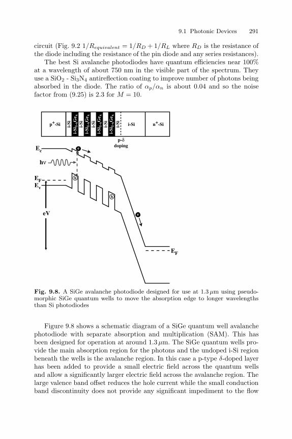
9.1 Photonic Devices 291
circuit (Fig. 9.2 1/Requivalent = 1/RD + 1/RL where RD is the resistance ofthe diode including the resistance of the pin diode and any series resistances).
The best Si avalanche photodiodes have quantum efficiencies near 100%at a wavelength of about 750 nm in the visible part of the spectrum. Theyuse a SiO2 - Si3N4 antireflection coating to improve number of photons beingabsorbed in the diode. The ratio of αp/αn is about 0.04 and so the noisefactor from (9.25) is 2.3 for M = 10.
Ec
Ev
p-δdoping
p+-Si
i-Si
1-xG
e x
i-Si
1-xG
e x
i-Si
1-xG
e x
i-Si
1-xG
e x
i-Si
i-Si
i-Si
i-Si i-Si n+-Sii-Si
EF
EF
eV e
e
h
h
hν
Fig. 9.8. A SiGe avalanche photodiode designed for use at 1.3 µm using pseudo-morphic SiGe quantum wells to move the absorption edge to longer wavelengthsthan Si photodiodes
Figure 9.8 shows a schematic diagram of a SiGe quantum well avalanchephotodiode with separate absorption and multiplication (SAM). This hasbeen designed for operation at around 1.3µm. The SiGe quantum wells pro-vide the main absorption region for the photons and the undoped i-Si regionbeneath the wells is the avalanche region. In this case a p-type δ-doped layerhas been added to provide a small electric field across the quantum wellsand allow a significantly larger electric field across the avalanche region. Thelarge valence band offset reduces the hole current while the small conductionband discontinuity does not provide any significant impediment to the flow

292 9. Optoelectronics
of electrons. This allows the diode to get closer to the ideal case of being aunipolar device at least in the absorption region.
Most SiGe p-i-n diodes which have been demonstrated in the literatureoperating at 1.3 or 1.55µm have been designed with speed as the main designparameter and the quantum efficiency has been traded off for high speedoperation. Typical examples have quantum efficiencies ranging between 10and 40% operating at frequencies of 2 GHz or above at room temperature.Significant improvements are required if these devices are to compete withthe present III-V diodes on the market place.
9.1.4 The Heterojunction Internal Photoemission Diode
p-Si
EF
Ev
Ec
∆Ev∆Eb
p+-Si1-xGex
p+-Si1-xGex
p-Si
hν
Fig. 9.9. A SiGe heterojunction internal photoemission diode using a p-type pseu-domorphic SiGe quantum well where the valence band discontinuity sets the wave-length response of the device
The heterojunction internal photoemission diode is based on excitation ofholes in a quantum well out of the well to form a photocurrent which can becollected. As such it is designed as a below-bandgap device and can operateat wavelengths greater than 1.67µ in the SiGe system when the valence bandis used. The basic structure, band structure and operation is shown in Fig.9.9. Results in the literature demonstrate the operation of such devices at77K between 3 and 5µm with quantum efficiencies of around 1%, dark cur-rents down to 10−8 A/cm2 and detectivity values of 109 cm(Hz)1/2/W whichis better than Schottky barrier Pt:Si photodiodes at 4µm. The performanceis not high enough to compete with the best III-V devices at such frequencies

9.1 Photonic Devices 293
and recent microbolometers fabricated using CMOS technology are substan-tially cheaper and perform with significantly better performance at 300Kand frequencies of 4 kHz in focal plane arrays.
9.1.5 Quantum Well Infrared Photodetectors (QWIPs)
For transitions above the bandgap energy of Si, SiGe or Ge then interbandp-i-n photodiodes can be used. Below the bandgap energy (0.66 eV for Ge)then intersubband transitions in quantum wells allow much longer wavelengthphotodetectors to be created (Fig. 9.1(d)). In particular in the mid- and far-infrared there are few practical semiconductors with appropriate bandgapsfor absorption or emission and intersubband transitions are then used. ForIII-V materials typically n-type QWIPs are used but for SiGe the valenceband is more appropriate with the large band offsets available in easily grownpseudomorphic quantum wells. As was demonstrated in Chap. 3, the subbandenergy levels can be approximated in the infinite well case to be
En =(n + 1)2 π2h2
2m∗w2for n = 0, 1, 2, 3, . . . (9.28)
demonstrating that the emission between 2 different subbands is controlledcompletely by the effective mass, m∗ of the carriers and the quantum wellwidth, w. This is only strictly true for unstrained materials. The strain inSiGe quantum wells also splits the valence band states and both heavy-hole(HH) and light-hole (LH) have different subband spacings in the quantumwell due to the strained and differing effective masses.
For intersubband transitions of HH to HH or of electron to electron, itcan be shown that the radiation only couples to the TM mode. Basicallythere is only a dipole matrix element (the integral in Fermi’s Golden rule(3.223) which determines the strength of the transition) for edge absorptioninto the quantum well as the electrons or holes have to oscillate in the ver-tical direction and through Maxwell’s equations the Pointing vector mustbe perpendicular to the dipole, hence only edge absorption is possible. Fora LH to HH intersubband absorption, the dipole has a finite component inthe plane of the quantum well and surface normal absorption is possible.A surface-normal QWIP is much easier to fabricate into arrays of detectors,hence in SiGe most demonstrations have been on the LH to HH intersubbanddetectors.
There are also the possibility of having bound-to-bound transitions andbound-to-continuum transitions (Fig. 9.10). QWIPs are typically set up ina similar manner to the p-i-n diode with vertical current transport but areunipolar. For the bound-to-bound transition shown in Fig. 9.10(a) the pho-toexcited electron in the upper, excited n = 1 level requires to either tunnelout of the quantum well or get excited out by thermionic emission if it is toform part of the photocurrent. The escape probability can be optimised if

294 9. Optoelectronics
Ec
E0
E1
w
hν = E1 -E0
thermionic emission
tunnelling
Ec
E0
E1
w
hν
continuum
(a) (b) Jp
(1-p)Jp
jp
Fig. 9.10. (a) A bound-to-bound transition where any photoexcited hole in E1 re-quires to either tunnel into the continuum or be thermally excited to the continuumto be extracted to the collector. (b) A bound-to-continuum transition in which thephotoexcited current density, jp has an effective capture probability of pc to remainin the quantum well. Therefore pcJp is the fraction of current captured by the welland (1 − pc) Jp as the remain current density transmitted to the next well in theQWIP
the excited subband state is designed to be close to the top of the quantumwell so that there is a small barrier to either tunnel or be thermally excitedout of the quantum well.
For a bound-to-continuum transition (Fig. 9.10(b)) there is a higher prob-ability of the holes being transported to the collector in the device but thedipole matrix element which determines the probability of a photon beingabsorbed and exciting a hole to the continuum state is less than in the bound-to-bound case. A simple analysis can be used to obtain the current in thephotodiode for both the bound-to-bound and bound-to-continuum case byusing the diagram in Fig. 9.10(b) where pc is defined as the effective cap-ture probability for an incident current density of Jp. We obtain pcJp as thefraction of the incident current which remains captured by the quantum wellwhile (1 − pc)Jp is the proportional of remaining current density which istransmitted to the next period. The incident infrared radiation of photonflux density, Φ0 creates a photocurrent,
jp = qηwΦ0 (9.29)
where ηw is the quantum efficiency of a single well. Using current continuitywe have
Jp = (1 − pc)Jp + jp (9.30)

9.1 Photonic Devices 295
Hence
jp = pcJp (9.31)
and the total net photocurrent is
Jp = qηΦ0G (9.32)
where G is defined as the overall photoconductive gain. For a structure withN quantum wells the total quantum efficiency is η = ηwN provided η 1since it is proportional to the absorption of the structure. The gain in theQWIP is therefore given by
G =1pc
ηw
η 1
pcN(9.33)
For the dark current density for a bound-to-bound transition, let us as-sume that only tunnelling allows carriers to escape from the quantum well.Then we have the transmission coefficient for tunnelling if the barrier fromthe excited subband, E1 to the top of the quantum well is EB of
T (E) = 1 for E > EB
= 0 for E < EB (9.34)
From Sect. 8.2 the dark current is obtained from the integral
Jdark = q
∫f (E) T (E) vdE (9.35)
which can be shown to be
Jdark = qv
(m∗kBT
πh2w
)exp
(−Ev − EF
kBT
)(9.36)
The important point from (9.36) is that the dark current decreases ex-ponentially as the temperature of the QWIP is reduced. Many QWIPs areoperated at 77K or using Peltier coolers due to this exponential dark currentdependence.
A number of surface-normal incidence SiGe QWIPs have been demon-strating operating in the important 8 to 12µm infrared atmospheric window.In particular using a buried silicide layer, higher responsivities than GaAsQWIPs have been demonstrated at significantly lower voltages potentiallyallowing very low power focal plane arrays. The buried silicide was demon-strated to increase the responsivity by a factor eight by acting as a substratereflector. The use of such silicide layers also reduced the dark current in suchdevices by around an order of magnitude. Again while the responsivities arebetter than some III-V technologies, better technologies do exist especiallythe new CMOS microbolometers which are already being fabricated into large

296 9. Optoelectronics
focal plane arrays and offer video rate (> 30 frames per second) imaging atroom temperature. These are broadband detectors (see Fig. 9.4) which aregood for a number of applications including firefighting and night vision.There are a few niche applications where the ability of the QWIP to distin-guish between different frequencies may allow them to obtain some marketshare.
9.2 The Quantum Cascade Laser
GaAs
p-AlGaAs
n-AlGaAs
p-GaAs
n-GaAs
light
cleaved(110)face
V
Energy
EcEv
eV
hν
EFn
EFp
Fig. 9.11. A schematic diagram of a GaAs / AlGaAs p-n diode laser along withthe appropriate bandstructure for the system. Electrons and holes recombine across
the bandgap and emit photons of frequency, υ =Eg
h
The final section in this chapter will be looking at a relatively new con-cept in the field of lasers and one which is potentially realisable in the Sisystem with heterostructure band engineering. This section is on unipolarlasers which are known as quantum cascade lasers since an electron cascadesdown a number of periods of the structure emitting photons. The first cascadelaser was demonstrated by Fredric Capasso and coworkers at Bell Labora-tories in 1992. The cascade idea is substantially different from the standardinterband p-n diode lasers made from GaAs and other direct bandgap III-Vmaterials for applications such as CD-ROMS and DVD players. These diodesbasically pull electrons and holes into the one quantum well layer (in a typeI system) between the p- and n- regions of the device where they recombine

9.2 The Quantum Cascade Laser 297
emitting a photon of energy corresponding to the bandgap energy dividedby Planck’s constant (Fig. 9.11). The indirect bandgap of silicon and SiGeprecludes the efficient recombination of electrons and holes for the emissionof photons as an appropriate phonon is also required.
Ec
E0
E1
E
w2
w2
z0
V0
0
hν = E1 -E0
Fig. 9.12. Intersubband emission between the upper state, E1 and the lower energystate, E0. A photon of frequency, ν = (E1 − E0) /h is emitted by this intersubbandtransition
The cascade laser uses intersubband transitions to emit photons (Fig.9.12). This allows much smaller energies to be realised, particularly in themid- and far-infrared regions of the electromagnetic spectrum. In addition,the emission frequency or wavelength can be tuned by the thickness of thequantum well and so one semiconductor material can be tuned to emit pho-tons over a wide range of the spectrum. This also allows lasers to be realisedin large parts of the electromagnetic spectrum where no materials exist withappropriate bandgaps for p-n diode lasers.
9.2.1 Basic Laser Physics
There are three main interactions light can have with semiconductors. In theprevious sections (9) the absorption process of a photon has been discussedwith regard to photodetectors. Fig. 9.13(a) shows the absorption process in aschematic diagram where a carrier is excited by the photon from a group state,E0 to an excited state E1 if the photon has frequency, ν > E/h. For a carriersitting in an upper energy level (Fig. 9.13(b)) this state is unstable. At sometime without any external influences it will make a transition to the groundstate emitting a photon in the process of frequency given by hν10 = E1 −E0.This is termed spontaneous emission and is the emission process in lightemitting diodes (LEDs). If a photon of energy hν10 is incident on the carrierin the upper energy state E1 then this photon can stimulate the emission of

298 9. Optoelectronics
another photon of the same frequency and phase (i.e. it is coherent with thefirst photon) with the carrier making a transition to the ground state (E0).This is the process in a laser. The radiation is monochromatic because allthe photons have energy hν10 and is coherent because all the photons are inphase.
Energy
initialstate
finalstate
finalstate
finalstate
initialstate
initialstate
(c) StimulatedEmission
(b) SpontaneousEmission
(a) Stimulated Absorption
E1
E0
Fig. 9.13. A schematic diagram of the photonic transitions between two energy(subband) states. (a) If a carrier in the lower level absorbs a photon of energycorresponding to the difference in the energy levels then the carrier can be excitedto the upper energy level. (b) If a carrier is in the upper level then it can fall tothe lower energy level emitting a photon with frequency ν = E/h where E is theenergy difference between the two levels. (c) If a carrier is in the upper level it canbe stimulated to fall to the lower level by another photon of frequency ν = E/hemitting a second photon of the same frequency which is coherent (in phase) withthe first photon
Let us assume that the instantaneous populations of the states, E0 and E1
are n0 and n1 respectively. Under thermal equilibrium and for (E1 − E0) >3kBT the population of the states is given by the Boltzmann distribution
n1
n0= exp
(−E1 − E0
kBT
)= exp
(− ν10
kBT
)(9.37)
as plotted using a dashed line in Fig. 9.15. As is consistent with a Boltzmanndistribution, there are more carriers in the lower energy states.
In the steady state, the stimulated emission rate and the spontaneousemission rate must be balanced by the rate of absorption to maintain thepopulations n0 and n1 constant. The transition rates between the states E1
and E0 can be calculated using Fermi’s Golden rule (3.223). It was Einsteinwho first defined the transition rate per incident photon for the transitionfrom E0 to E1 as
B01 =2π
h
∣∣∣〈ψ1| H |ψ0〉∣∣∣2 (9.38)

9.2 The Quantum Cascade Laser 299
The stimulated emission rate is proportional to the photon-field energydensity in the system defined as ρ (hν01). The stimulated emission rate cantherefore be written as B10n1ρ (hν01). The spontaneous emission rate fromE1 to E0 is defined as A10n1 with A10 a constant and is independent of thephoton density. A and B are named the Einstein coefficients. The absorp-tion rate is proportional to the carrier population in the lower level and thephoton-field energy density. Hence it is given by B01n1ρ (hν01). In the steadystate we have
stimulated-emission rate + spontaneous-emission rate = absorption ratethat is
B10n1ρ (hν01) + A10n1 = B01n1ρ (hν01) (9.39)
Distance
losslossgain
Opticalfielddistribution
Refractiveindex
Fig. 9.14. Modal confinement into a ridge waveguide using a change in refractiveindex between the semiconductor and air
For a laser it is stimulated emission that we are interested in dominatingover spontaneous emission. Therefore rewriting equation 9.39 as
stimulated − emission− ratespontaneous− emission − rate
=B10
A10ρ (hν01) (9.40)
it is clear that to enhance the stimulated emission, the photon-field densityrequires to be very large. The easiest way to enhance the photon-field densityis to produce a resonant optical cavity. The simplest type of cavity is a Fabry-Perot ridge waveguide (Fig. 9.14) where a ridge is etched out of the activesemiconductor material. The refractive index change between the semicon-ductor and air is enough to reflect around 30% of the radiation at each facet.Hence along the length of the cavity standing wave modes are set up suchthat the frequency ν = c/2L where L is the length of the cavity and c is thespeed of light in the medium.

300 9. Optoelectronics
EnergyE2
E1
E0
EquilibriumBoltzmanndistribution
Population of states
Pumping
Rapiddecay
Lasertransition
ν =E1– E0
h
Fig. 9.15. The basic concept behind a three level laser population inversion scheme.In thermal equilibrium the population of states for a number of subbands in a quan-tum well is a Boltzmann distribution which results in significantly higher numberof states in the lower energy subbands. For a laser, a higher number of states is re-quired in the upper state of the laser transition (in this case between E1 and E0).Toachieve this, some mechanism is required to pump electrons into a higher energystate (E2) where the electrons may relax into E1. If the lifetime of the upper lasertransition state, E1 is made longer than either E2 or E0 then population inversionoccurs. This creates a plentiful supply of carriers for the laser transition. In mostlasers, a fourth state which is lower than E0 is used to create fast depopulationof E0 to give the required lifetime difference between E1 and E0 for populationinversion
Equation (9.39) can also be rearranged to give
stimulated − emission − rateabsorption− rate
=B10
B01
n1
n0(9.41)
Therefore for the stimulated emission to dominate over the absorption ofphotons, the upper energy state, E1 requires a larger population of states thanthe lower energy state, E0 i.e. population inversion. This normally requires atleast three energy levels rather than two to guarantee population inversion.Carriers are pumped either optically or electrically from the lowest energystate to a higher energy state, E2 (Fig. 9.15). This pumping changes thepopulation density of the states from the thermal equilibrium Boltzmannpopulation. Provided the lifetime of the upper E2 states is much shorterthan the upper laser transition state, E1 then the population of E1 will begreater than E2. In a similar fashion the lifetime of E0 requires to be shorterthan E1 for population inversion. While pumping can achieve this, the typical

9.2 The Quantum Cascade Laser 301
ν
Irradiancebroadened lasertransition line
frequency, ν
Irradianceaxial modes inlaser output
ν
Irradiancecavitymodes
c2L
(a)
(b)
(c)
Fig. 9.16. The cavity modes as the laser achieves threshold. (a) is the output fromthe intersubband transition being used for the laser (i.e. the E1 to E0 transitionin Fig. 9.15). This electroluminescence is extremely broad compared to a laser. (b)is the cavity modes from a simple ridge waveguide Fabry-Perot cavity. The endsof the ridge reflect the light creating cavity modes with frequency spacing of c/2Lwhere L is the length of the ridge. (c) When threshold is reaches, the laser emitsa convolution of (a) the electroluminescence and (b) the cavity modes to producethe output demonstrated in (c)
way of achieving this in real systems is to have a fourth energy level belowE0 which is used to create fast depopulation of E0 and then the pumpingis from this fourth state. This decouples the pumping mechanism from thelower energy state of the laser transition.
Once a cavity has been fabricated and an active semiconductor het-erostructure with population inversion has been placed in the cavity, thecavity modes (Fig. 9.16(b)) will convolve with the broadened electrolumines-cence spectrum of the transition E1 to E0 (Fig. 9.16(c)) forming the laserspectrum shown in Fig. 9.16(c). This is a Fabry-Perot cavity mode spectrumwith 4 sharp peaks corresponding to the modes along the length of the cavity.
To achieve lasing, the current needs to be increased in the system so thatthe density of carriers and the population inversion can increase to increasethe stimulated emission in the cavity. Below threshold the spectrum of thelaser is a broad electroluminescence (Fig. 9.17(b)). As threshold approaches,the gain in the cavity starts to overcome the losses and absorption of photonsand the broad spectrum starts to narrow with the cavity modes beginningto be observed convoluting the broad electroluminescence spectrum (Fig.

302 9. Optoelectronics
Thresholdcurrent
Lightoutputpower (L)
CurrentL
spontaneousemission
frequency, ν
L
threshold
L
stimulatedemission
(a)
(b)
(c)
(d)
frequency, νfrequency, ν
Fig. 9.17. A demonstration of the threshold of a laser
9.17(c)). Once above threshold the power of the laser increases substantiallyas the optical gain in the cavity amplifies the output power (Fig. 9.17(a)) andthe emission spectrum involves a very sharp δ-function like peak (Fig. 9.17(d))or peaks if multiple Fabry-Perot modes can be supported (Fig. 9.16(c)).
9.2.2 The Si/SiGe Quantum Cascade Laser
The original quantum cascade lasers were fabricated in a number of differentIII-V heteromaterials. The first laser operated in the mid-infrared but morerecently the concept has been expanded and quantum cascade lasers emitradiation across the electromagnetic spectrum from around 2 THz (150µm)to ∼ 2 µm wavelength (150THz). Figure 9.18 shows the typical heterolayerstructure of a III-V quantum cascade laser. Only three periods are shownbut it should be clear from the diagram why it is called a cascade since theelectrons cascade down the heterolayers. In this particular structure mini-bands and minigaps are used. These are the same as the bands and bandgapsin semiconductors but are created by the heterolayers. If quantum wells areplaced close enough together with thin barriers between the wells that allowsthe wavefunctions of carriers in each well to overlap as in the tight bindingmodel (Sect. 3.2.5) then minibands and minigaps are formed from the artifi-cially grown heterostructure in the same manner to bandgaps and bands insemiconductors. Hence carriers have allowed and disallowed energies in thequantum wells in addition to the subband states. These can be used to greateffect as an injector of electrons into a subband state which is designed to bethe upper state of a laser transition.

9.2 The Quantum Cascade Laser 303
Miniband
E2
E1
E0
e-
Miniband
E2
E1
E0
e-
Miniband
E2
E1
E0
e-
Emittertransition
region
Injector
Injector
Emittertransition
region
Injector
Ec
hν = E2
- E1
Fig. 9.18. A schematic diagram of the conduction band in a three period cascadeemitter. The injector region is designed to pull the electrons from an emitted activeregion back to the upper level in the next active region. The whole structure isdesigned so that the bands align when an appropriate electric field is placed acrossthe whole structure
For a single quantum well emitter, the power is proportional to the fre-quency of the emitted radiation. For visible frequencies this provides no prob-lems with laser powers. As the frequency is reduced, however, the power isalso reduced in a linear fashion. The advantage of the cascade is that a num-ber of periods, N can be used (Fig. 9.18) and the power scales as the numberof periods. Therefore the power is given by
P = NηI − Ith
2ehυ (9.42)
where I is the applied current, Ith is the threshold current for lasing and η isthe power efficiency. This is extremely important for far-infrared or terahertzlasers where the frequency can be a thousand times lower than the visiblepart of the electromagnetic spectrum. Hence the power output is predictedto be very low. By having a large number of periods, that is a few hundredactive periods, the power can be scaled back up much closer to the poweroutput from visible p-i-n lasers.
The most important part of the heterolayer design in a quantum cascadelaser is to design a structure which allows population inversion between twoenergy subbands in quantum wells. There are a number of different ways thiscan be achieved. Fig. 9.19 shows two standard ways of achieving populationinversion. The first in Fig. 9.19(a) uses a diagonal or interwell laser transi-tion followed by two wells to produce fast depopulation of the lower lasertransition state, E1. Above the optical phonon energy of 62meV in Si, fast

304 9. Optoelectronics
electronsEc
Injector
Collector
Emittertransition
hν = E2 - E1
E0
E1
E2Ec Injector
Collector
Emittertransition
E0
E1
E2
hν = E2 - E1electrons
(a) (b)
Fig. 9.19. A schematic diagram of the original quantum cascade lasers. (a) Ainterwell or diagonal transition between two different quantum wells is used for thelaser transition between E2 and E1. A third well is then used for fast depopulationof the lower laser transition state to produce population inversion. (b) Above theoptical phonon energy, this can be used for fast depopulation if the E1 and E0 levelsare spaced by the LO optical phonon energy, ELO. A vertical transition in the onequantum well between E2 and E0 can then be used for the laser transition whichhas a larger matrix element and hence stronger emission
depopulation of the lower laser transition state can be achieved by makingthe two lower energy subbands spaced by the optical phonon energy ELO.This produces a very fast resonant depopulation (Fig. 9.19(b)) and hencepopulation inversion can be achieved. The added advantage is that a verticalor intrawell laser transition can be produced which has a larger matrix ele-ment for the intersubband transition if calculated from Fermi’s Golden rule(3.223) resulting in higher efficiency and therefore higher power operationfrom the laser.
There are a number of other possible mechanisms. In SiGe it is the valenceband which is typically studies for quantum cascade laser because the valenceband offsets are larger than the conduction band offsets for small Ge frac-tions and the high electron effective mass in the tunnelling direction forcesextremely thin (<0.5 nm) quantum mechanical tunnel barriers if significanttunnelling is required. As this is not easy to achieve in the conduction bandof Si/SiGe, hole cascades are being studied. Figure 9.20 shows four differ-ent active regions which can be achieved using Si/SiGe heterostructures. Thefirst (Fig. 9.20(a)) is the resonant LO optical phonon depopulation previouslystudied by this time designed for the valence band. The second, Fig. 9.20(b),is a diagonal transition. The third is a miniband design, Fig. 9.20(c), whichhas the added advantage of laser transitions over a number of quantum wells.This improves the matrix element calculated from Fermi’s Golden rule andhence improves the current and therefore the efficiency and power output ofthe device as more than one quantum well can emit photons. The final designshown here is a negative effective mass design, Fig. 9.20(d). The idea is touse the strain in a SiGe quantum well to split the LH and HH states. The

9.2 The Quantum Cascade Laser 305
hole
Injector
Collector
Emittertransition
Ev
ELO
Injector
Collector
Emittertransition
holeEv
hole
Ev
miniband1
miniband2miniband injector
Emittertransition
k
HH1
LH1
hole
Ev
Injector
Collector
E
HH2
(a) (b)
(c) (d)
hν
hνhν
hν
Fig. 9.20. (a) a resonant optical phonon depopulation active quantum cascaderegion. (b) an interwell or diagonal quantum cascade active region. (c) a minibandquantum cascade active region. (d) a negative effective mass quantum cascade activeregion
strain is then chosen through the Ge content to try and push the LH1 statehigher in hole energy (i.e. lower in real or electron energy so down the page)above the HH2. As this is forbidden from the quantum mechanics selectionrules (i.e. the matrix element in Fermi’s Golden rule is zero) the LH1 bandproduces an anti-crossing and it bends up in real energy i.e. down to a lowerenergy state for holes. Therefore tunnelling into a quantum well must hap-pen at k = 0. Scattering from the SiGe alloy can scatter the hole to the holeminimum in k−space where the laser transition can occur from the LH1 toHH1 state before the hole is alloy scattered back to k = 0 and it can tunnelto next quantum well.
Figure 9.21 shows an transmission electron micrograph of a negative effec-tive mass quantum cascade emitter grown using SiGe heterostructures. Thelight areas are tensile strained-Si barriers and the darker regions between thebarriers are Si0.72Ge0.28 quantum wells grown on top of a Si0.8Ge0.2 virtualsubstrate. The structure was grown using LPCVD with boron doped con-tacts on either side of the quantum wells and barriers. Fig. 9.22 shows theelectroluminescence from the edge of the fabricated device. The spectrum hasbeen taken using a Fourier transform infrared spectrometer using a cooledSi-bolometer as a detector for the far-infrared (terahertz) radiation. A largervoltage has been applied across the device than that required to line up theappropriate subband states in neighbouring quantum wells. This allows all

306 9. Optoelectronics
Fig. 9.21. A transmission electron micrograph of a strain symmetrised quantumcascade emitter designed for a negative effective mass transition. The light areas are5 nm thick tensile strained-Si barriers and the darker regions between the barriersare 8 nm Si0.72Ge0.28 quantum wells grown on top of a Si0.8Ge0.2 virtual substrate.The structure has 30 active quantum wells
0.0
0.2
0.4
0.6
0.8
1.0
Energy (meV)
Edg
e em
itte
d sp
ectr
al p
ower
(a.
u.)
Frequency (THz)0 4 8 12 16
7.0 V @ 10% dutycycle4.2 K
LH1–HH1
LH2–HH1
HH2–HH1
20
10 20 30 40 50 60 70 800 10090
Fig. 9.22. The edge electroluminescence from a Si/SiGe negative effective massquantum cascade emitter at 4.2K with 7 V applied bias. The LH1 to HH1 and HH2to HH1 transitions are clearly visible. The dotted lines are the theoretical calculatedspectrum from k.p theory
the intersubband transitions including higher energy ones to be mapped out.In the edge emission LH to HH and HH to HH transitions can be observed.As was previously discussed with regard to polarisation, HH to HH transi-tions can only be observed in the edge or TM mode. Therefore by observingthe surface-normal emission, only the LH to HH transition should be ob-served. This is indeed what is observed in experiments as shown in Fig. 9.23.The advantage of such surface-normal emission is that vertical cavity surface

9.2 The Quantum Cascade Laser 307
emitting lasers (VCSELs) may be fabricated into arrays of lasers which areideal for imaging applications.
0.0
0.5
1.0
1.5
2.0
2.5
3.0
3.5
0 10 20 30 40 50 60 70 80
0 4 8 12 16Frequency (THz)
Energy (meV)
Surf
ace-
norm
al e
mit
ted
pow
er (
a.u.
)
LH1-HH1
Fig. 9.23. The surface-normal electroluminescence from the negative effective massquantum cascade emitter with 4V applied across the structure. The dotted line isthe theoretical spectrum calculated using k.p theory
0 2 4 6 8 10 12 14 16 18 20
3.8 V 6.4 V
0
5
10
15
20
Energy (meV)
Edg
e em
issi
on s
pect
ral i
nten
sity
(a.
u.)
3.5 4.54.0 5.0 5.5 6.0 6.5
5.05.56.06.57.07.58.0
Applied voltage (V)
Pea
k en
ergy
(m
eV)
Fig. 9.24. A diagonal or interwell intersubband transition between a LH1 and aHH1 state in neighbouring quantum wells. On the left are two different spectrumfor two different applied voltages across the 100 period quantum well structure.As expected for a diagonal transition, the peak shifts to higher energy as the biasacross the wells is increased. The insert on the right demonstrates how the centreof the peak shifts as the bias is increased

308 9. Optoelectronics
In addition to negative effective mass transitions, diagonal transitionshave also been demonstrated in the Si/SiGe system. Figure 9.24 shows a spec-trum from interwell intersubband transitions between strain-symmetrised4.4 nm Si0.7Ge0.3 compressively-strained quantum wells with 2.2 nm tensile-strained-Si barriers grown on Si0.8Ge0.2 virtual substrates. As the voltageacross the 100 period structure is increased, the peak shifts as the alignmentof the subbands is increased. The movement of the peak with increasing volt-age is demonstrated in the insert to Fig. 9.24 on the right hand side.
4 K30 K60 K100 K150 K200 K250 K300 K
0 100 200 300
0.05
0.04
0.03
0.02
0.01
0.00
–0.01
–0.02
Delay (ps)
Tra
nsm
issi
on c
hang
e (a
.u.)
Fig. 9.25. Non-radiative lifetime measurements on a Si/SiGe quantum cascadeemitter structure with Si0.7Ge0.3 compressively-strained quantum wells. A free elec-tron laser is used to excite carriers to the upper LH1 state and then a time resolvedabsorption measurement is used to obtain the non-radiative lifetime. Unlike theGaAs results, the non-radiative lifetime is constant at around 30 ps between 4Kand 300 K
While to date no Si/SiGe quantum cascade lasers have been demon-strated, particularly for terahertz lasers the Si-based lasers have the potentialto be far superior to III-V terahertz lasers. In group IV materials there is nopolar optical phonon scattering below the optical phonon energy of around62meV. In III-V materials, the electrical dipole between a group III atomand a group V atom results in the additional phonon scattering mode termedpolar optical phonon scattering. For quantum cascade lasers this results inthe non-radiative lifetime between the laser transition states having a verystrong temperature dependence. For lasing the non-radiative transition re-quires to be significantly longer than the radiative transition so that theradiative transition (i.e. the photon emission) dominates the device. Mea-surements have shown that above about 40K in GaAs quantum wells, polaroptical phonon scattering dominates and the non-radiative lifetime collapses.Hence III-V terahertz quantum cascade lasers can only operate at present

9.3 Further Reading 309
at relatively low temperatures. Fig. 9.25 shows results from Carl Pidgeonat Heriot-Watt University where the non-radiative lifetime has been mea-sured in compressively-strained Si0.7Ge0.3 quantum wells. Unlike the GaAsresults, the non-radiative lifetime is longer than the III-V results but it is alsoapproximately constant between 4K and 300K. This bodes well for roomtemperature operation from Si/SiGe terahertz quantum cascade lasers.
9.3 Further Reading
1. S.L. Chuang, Physics of Optoelectronic Devices, John Wiley and Sons,New York (1995)
2. J.H. Davies, The Physics of Low Dimensional Structures” CambridgeUniversity Press (1998)
3. M.J. Kelly, Low Dimensional Semiconductors: Materials, Physics, Tech-nology Devices, OUP, Oxford (1995)
4. L. Pavesi, J. Phys.: Condens. Matter 15, R1160 (2003)5. S.M. Sze, Physics of Semiconductor Devices 2nd Edition, John Wiley and
Sons, New York (1981)6. S.M. Sze Semiconductor Devices: Physics and Technology 2nd Edition,
John Wiley and Sons, New York (2002)7. D.J. Paul, Semiconductor Science and Technology 19, R59 (2004)

10. Integration
This chapter is devoted to the fabrication processes involved in producingcomplete systems in addition to providing a brief overview of typical circuitarchitectures used for different applications. Much of the chapter will bedevoted to conventional technology particularly with bipolar, HBT, CMOSand BiCMOS although more modern systems such as RTDs and fault tolerentarchitectures will also be briefly reviewed.
10.1 The CMOS Inverter and MOS Memory Circuits
n-transistor p-transistor
Fig. 10.1. The representations of the n- and p-MOS transistors as drawn in circuitarchitecture diagrams
CMOS is the most common circuit architecture used in modern micro-electronics. It is based on the combination of p-MOS and n-MOS which havethe circuit symbols shown in Fig. 10.1. By combining the n- and p-MOStransistors in different ways, all standard logic gates can be fabricated withappropriate numbers of transistors. By combining the standard logic gatesinto simple or complex circuits, real products ranging from microcontrollersto complete single chip computers can be designed. The most important logicgate is the CMOS inverter (Fig. 10.2) which only consists of one n- and onep-MOS device (Fig. 10.2(a)). Any input voltage, Vin of ’1’ is translated intoa Vout of ’0’ and vice versa. The circuit symbol for an inverter is shown inFig. 10.2(b).
The importance of CMOS circuits and the CMOS inverter becomes clearwhen the power dissipation of the inverter is considered. All other CMOSlogic gates dissipate power in a similar manner to the inverter, therefore un-derstanding the inverter will provide a general basis for CMOS logic circuits.

312 10. Integration
p-MOS
n-MOS
Vin Vout
VDD(a) (b)
Vin Vout
CL
Fig. 10.2. (a) A schematic diagram of the CMOS inverter with one p-MOS andone n-MOS transistor. (b) The circuit symbol for an inverter. When an inverter isconnected to the rest of the circuit by interconnects, a load capacitance results asshown by the dashed capacitor in (a)
There are three main parts to the power being dissipated in the inverter.The first is the static power dissipation which is the power dissipated whenno switching is taking place. This is solely related to the sum of all leakagecurrents in the transistors or interconnects, Ileakage and the applied voltage,VDD as
Pstatic = ΣIleakageVDD (10.1)
For an ideal device and circuit technology the leak current should be zero.In reality it is always finite and correspond to the Ioff of each transistorwhich for MOSFETs depends on the subthreshold slope, S and the thresholdvoltage, VT as
PstaticMOS = VDDIonW10−VT /S (10.2)
for transistor of gate width, W . MOS devices (Ioff ) have the lowest leak-age currents of any technology while for MODFET or MESFET technology,the off currents are orders of magnitude higher due to the poorer isolationbetween the source and drain. Also Schottky gates have higher leakage cur-rents than gates with insulator layers such as silicon dioxide. For a CMOSmicroprocessor with a million 0.25µm transistors operating at 3 V, this staticcontribution corresponds to a few milli-Watts of power. The power consumedby switching or dynamic power dissipation is significantly higher at least forCMOS technologies of 90 nm or higher. As the gate oxide is reduced below1.5 nm the static power dissipation grows significantly and for deep submicronCMOS technologies may dominate.
The dynamic power dissipation may be considered by assuming that theinterconnect of the output of the inverter has a load capacitance of CL (Fig.

10.1 The CMOS Inverter and MOS Memory Circuits 313
10.2(a)). When the load capacitor is charged during the low-to-high transitionthrough the p-MOS, the voltage of the load capacitor rises from 0 to VDD.While part of the energy is stored in the load capacitor, most of the poweris dissipated into the p-MOS transistor. For the high-to-low transition, thecapacitor is discharged and the stored energy is dissipated through the n-MOS device. Therefore if the gate is switched on and off at a frequency, fc
per second, the dynamic power consumption is
Pdynamic = CLV 2DDfc (10.3)
Frequently a factor a2 is also added to the above equation where a represents
the transition probability of the logic gates.There is a third element to the power dissipation of a CMOS inverter.
There is a finite time for the inverter to switch between the on and off statesor vice versa. When the inverter is switching between the two states, boththe n- and p-MOS transistors are dissipating dc power in the circuit. As thecurrent is varying and different types of clock pulses are used for differentapplications, the easiest way of considering a general term for this powerdissipation is to consider an average current during the switching of Imean
and then the short circuit power dissipation is given by
Pshort−circuit = ImeanVDD (10.4)
The short circuit term can generate noise by leakage into the substrate. Thiscan couple to power supply buses or the semiconductor substrate and isresponsible for cross-talk, where the digital and analogue parts of a circuitcouple to each other creating errors. By careful design of the threshold voltageand VDD, these effect can be minimised.
The total power dissipation of the CMOS inverter is the sum of the threeterms giving
Ptotal = ΣIleakageVDD + CLV 2DDf + ImeanVDD (10.5)
The power is predominantly dissipated in the form of heat. Modern micro-processors with millions of transistors actually operate at up to 100 oC, sig-nificantly above room temperature. All this heat needs to be dissipated eitherthrough the substrate or the interconnects. Most of the dissipation is throughthe substrate and therefore the thermal conductivity of the substrate is animportant parameter in microprocessors. The amount of heat which can bedissipated actually determines the integration density of the transistors as ahigher density would result in the substrate being too hot for the transistorsto operate with lower error rates.
The inverter is the simplest CMOS circuit but three or more terminalgates are required if any type of logic operation is to be performed. If aNAND gate can be fabricated then every other standard logic gate can becreated by combining NAND gates. For instance, if the two input terminalsare tied together then an inverter is created. Examples of CMOS NAND

314 10. Integration
VDD
input A
input B
output
input Ainput B
output
(a)
(b)
input Ainput B
output
(c)
A B output
0011
0 11 1
10
01
Fig. 10.3. (a) The circuit diagram of a NAND gate along with (b) the standardcircuit symbol and (c) an alternative circuit symbol
VDD
input A
input B
output
(a)(b)
input Ainput B
output
A B output
0011
0 11 0
00
01
Fig. 10.4. (a) The circuit diagram of a NOR gate along with (b) the circuit diagram
and NOR gates are shown in Figs. 10.3 and 10.4 respectively. Both thesegates can be expanded to have N input gates rather than two. Most modernmicroprocessors will not just use inverters, NANDs and NOR gates. The realpower of CMOS circuit design is the ability to design complex functions inan efficient manner using n- and p-MOS transistors.
In addition to switching and logic, microprocessors also require memory.In modern computing, data is transfered from one memory location, a logicoperation is performed and then the answer is written into another mem-

10.1 The CMOS Inverter and MOS Memory Circuits 315
VDD
Wordline
Bitline
Bitline
SRAM6 transistors
Wordline
Bitline
DRAM1 transistor
Capacitor
Wordline
Bitline
Flash1 transistor
Capacitor
(a) (b) (c)
Fig. 10.5. Schematic diagrams of (a) static random access memory, (b) dynamicrandom access memory and (c) flash memory
ory location. By combining these operations with different logic operations,a general microprocessor can be programmed to perform most tasks by re-configuring different standard operations. Therefore memory is also very im-portant. Figure 10.5 shows schematic diagrams of the three most importanttypes of memory, (a) SRAM, (b) DRAM and (c) flash.
Dynamic random access memory (DRAM) is the cheapest and has thelowest static power but needs to be refreshed very frequently. It is also verydifficult to integrate with high speed CMOS transistors on a microproces-sor as the capacitor structure requires significantly different processing fromthe transistor. Therefore static random access memory (SRAM) is typicallyused on most microprocessors. It is significantly faster than DRAM or flashbut consumes much more power (both static and dynamic power). Flashmemory is non-volatile but is slow and requires a large voltage to write oper-ations. Flash memory is used in mobile phones and portable devices as a largeamount of energy is required to write to the memory but being non-volatile,no energy is required to maintain the information. Only a small amount ofenergy is consumed in the reading process compared to DRAM or SRAM.The typical structure has a poly-Si floating island inserted into a MOSFETbetween the main gate and the channel. By applying a large voltage to thegate, the island can be charged and the threshold of the MOSFET changes.Therefore applying a source-drain bias will produce a readout dependent onthe charge on the island.
We will finish this section by showing how tunnel diodes such as RTDscan be made into memories. Figure 10.6 shows a schematic of a tunnellingstatic random access memory (TSRAM). The two RTDs operate to createa charging node between them. The advantage of the TSRAM is that the

316 10. Integration
word line
bit line
writeFET
readFET
loadFET
Vout
VDD
VDDMemory
CellRTD
RTD
Fig. 10.6. The circuit diagram for a tunnelling static random access memory
static power dissipation is significantly lower than SRAM, DRAM or flashwhile operating speeds comparable to SRAM can be obtained. In particu-lar, the number of transistors and device is significantly lower than a CMOSSRAM which partially accounts for the reduction in power. To some extentthe RTDs are operated as capacitors with the back to back current-voltagecharacteristics creating two stable points for the ’1’ and ’0’ at the valley ofeach RTD. No demonstration of such a circuit has been achieved in silicontechnology although III-V devices have shown very low static power dissipa-tion and high switching speeds. Table 10.1 compares the main parameters indifferent types of memory. Standby power is becoming an important param-eter especially as the minimum feature size is reduced and leakage currentsare increasing. Speed is also important especially for the memory on a mi-croprocessor which now accounts for over 80 % of the transistors.
10.2 Silicon Process Technology
Most of the thin film deposition or epitaxial growth methods required forfabricating different silicon-based devices were discussed in Chap. 2. In thissection the remaining techniques required for fabricating different silicon-based devices will be briefly reviewed before a number of standard processeswill be demonstrated.

10.2 Silicon Process Technology 317
Table 10.1. A comparison of a number of the main parameters affecting the per-formance of different types of memory
Technology Access Retention Speed Density Standbytime time (GHz) (Mbit/cm2) power
(1-2 µm (W/Mbit)pitch)
16 MB 1 ns >10 years 0.03 5 to 10 0.01SRAM to 0.1
256 MB 10 ns <256 ms 0.01 60 to 150 2 ×10⁻⁴
DRAM to 0.02
256 MB 10 ns >10 years 0.01 60 to 150flash to 0.02
256 MB 1T 10 ns >10 years 0.01 50 to 100 10−9
Si TSRAM to 0.04
256 MB 1Tstrained-Si 4 ns >10 years 0.03 50 to 100 10−9
TSRAM to 0.12
10.2.1 Thermal Oxidation
Thermal oxidation is one of the key processes which may be used manytimes in the fabrication of a device. Not only is it used for the gate oxide inMOSFETs but is also used for insulating layers to electrically isolate devices.There are two main types of oxidation reaction termed dry and wet whichare respectively
Si (solid) + O2 (gas) −→ SiO2 (solid) (10.6)
Si (solid) + 2H2O (gas) −→ SiO2 (solid) + 2H2 (gas) (10.7)
Wet oxidation is faster than dry and is used for thick oxide layers such aselectrical isolation. Dry oxidation has a lower interface state density which isimportant as the interface states can trap electrons and degrade the electricalproperties at the interface. Good oxides are amorphous in nature and haveinterface state densities of around 1014 m−2 for thermal gate oxides. TheSi/SiO2 interface is constantly moving into the silicon as the oxide is grownwith any contamination on the original surface ending up on the top of theoxide surface. Hence the technique can end up with high quality interfaceswith few impurities or trapped charges. Fast diffusers such as sodium or goldcan get to the interface at relatively low temperature and therefore suchimpurities must be kept well away from silicon processing.
Thermal oxidation of SiGe also creates problems as a number of detri-mental effects occur. It is worthwhile noting that germanium oxide is water

318 10. Integration
soluble which is not ideal for many of the silicon processing steps where wa-ter is the solvent. The second is that an electrical defect is created in thesilicon dioxide for every Ge atom that is incorporated as germanium oxide.Even at quite low concentration of Ge in the layer being oxidised can endup creating a surface state density comparable to the electron charges at theinterface in a MOSFET. A third effect is called snow-ploughing where as theSi/SiO2 interface moves further into the SiGe layer, not all the germaniumis incorporated in the oxide film and a higher concentration of Ge is driveninto the substrate in front of the oxide interface. All these effects result indevices having to be designed where either a deposited oxide must be usedor a silicon cap is required which can be consumed during oxidation.
dsilicon
Co
Ci
x
Cgas SiO2Cg
F1 F2 F3
Fig. 10.7. The Deal and Grove three stage model of oxidation. F1 is the flux fromthe flow of gas stream to the surface. F2 is the flux of the diffusion of oxidisingspecies through the formed oxide and F3 is the flux for the reaction at the Si - SiO2
interface. The concentration of the oxidising species varies from Cg in the gas toC0 at the oxide surface and Ci at the Si - SiO2 interface
The kinetics of thermal oxidation of silicon were first described by Dealand Grove in 1965 and form a three stage process (Fig. 10.7). For oxidationthe oxidant must: (1) travel from the gas phase to the gas-oxide interfacewith flux F1, (2) move across the SiO2 film towards the silicon with flux, F2
and (3) react with silicon at the Si / SiO2 interface with flux F3. The modelassumes that the oxidation process is in the steady state and therefore allthe fluxes must be equal (i.e. F1=F2=F3=F ).
The gas-phase oxidant flux,F1, is given by
F1 = h (C∗ − C0) (10.8)

10.2 Silicon Process Technology 319
where h is the gas-phase mass-transport coefficient, C0 is the oxidation con-centration in the oxide at the outer surface and C∗ is the equilibrium oxidantconcentration in the oxide. Henry’s law is used to relate the partial pres-sure of the oxidant in the gas at pressure, p with the equilibrium oxidantconcentration in the oxide as
C∗ = kp (10.9)
where k is the Henry’s law constant. This law only holds when the oxidantdoes not associate or dissociate at the outer surface, implying the oxidant ismolecular.
Transport of the oxidising species to the Si - SiO2 interface occurs bydiffusion in a similar fashion to electron and hole diffusion described in earlierchapters. The flux of the diffusing species can be written as the product ofthe concentration gradient across the oxide, (C0 − Ci) /xox. Fick’s law is thenused to describe the flux of oxidant across the oxide layer as
F2 =Dox (C0 − Ci)
xox(10.10)
where Dox is the diffusivity, Ci is the concentration of oxidising species atthe Si/SiO2 interface and xox is the oxide thickness. The flux correspondingto the reaction at the Si/SiO2 interface is given by
F3 = ksCi (10.11)
where ks is the chemical reaction rate constant.By solving the above equations for the flux, the oxide growth rate, Rox
may be determined from
Rox =dxox
dt=
F
Nox=
ksC∗/Nox
1 + ks/h + ksxox/Dox(10.12)
where Nox is the number of oxidation molecules incorporated per unit volumeinto the oxide. Solving this differential equation while assuming that an initialthickness of oxide (xi) may be present (xox = xi at t=0), results in thefollowing equations for the oxide thickness as a function of time, t
xox =A
2
⎡⎣√√√√(
1 +t + τ
A2
4B
)− 1
⎤⎦ (10.13)
where the standard variables as used for oxidation have been defined as
A = 2D
(1ks
+1h
)(10.14)
B =2DoxC∗
Nox(10.15)
τ =xi + Axi
B(10.16)

320 10. Integration
The parameter τ is used to include any initial oxide thickness that ispresent on the surface. If the oxidation time is short then F3 is the ratelimiting step and (10.13) can be approximated by a linear relationship of
xox =B
A(t + τ) (10.17)
The fraction B/A is termed the linear rate coefficient and is related tobreaking the bonds at the Si/SiO2 interface. The values will therefore dependon the crystal orientation of the surface. The linear rate coefficient is smallerfor the Si(100) surface compared to the Si(111) surface since the later hasfewer bonds between adjacent planes.
10-4
10-3
10-2
10-1
100
101
102
10-3
10-2
10-1
100
0.65 0.7 0.75 0.8 0.85 0.9 0.95 1 1.05
1000/T (K–1
)
Lin
ear
Rat
e C
oeff
icie
nt B
/A (
µm/h
r)
Parabolic R
ate Coefficient (µm
2/hr)
B wet
B/A wet (EA=1.96 eV)
B/A dry (EA=2.0 eV)
B dry
1200 1100 1000 900 800 700
Temperature (˚C)
Fig. 10.8. The variation of the linear and parabolic rate coefficients with inversetemperature. Both wet and dry data are at pressures of 8.5 × 10⁴ Pa
For long oxidation times (10.13) reduces to the parabolic form
xox =√
B (t + τ) ≈√
Bt (10.18)
The coefficient B is therefore termed the parabolic rate coefficient and de-pends on the diffusion across the already formed oxide layer. Since SiO2
is amorphous it does not depend on crystal orientation. Both the linear andparabolic coefficients are shown in Fig. 10.8. Figure 10.9 shows plots of (10.13)for both wet and dry oxidation for a number of different oxidation times. The

10.2 Silicon Process Technology 321O
xide
thi
ckne
ss (
µm)
800˚C dry
920˚C dry1000˚C dry1100˚C dry
920˚C wet1000˚C wet1100˚C wet
1 2 3 4 5 100.1 0.2 0.3 0.5Time (hours)
10-3
10-2
10-1
100
101
Fig. 10.9. The thickness of oxides as a function of growth time for a number ofdifferent temperatures. Both wet and dry oxidation is shown
figure clear demonstrates the faster oxide growth in wet oxidation comparedto dry.
10.2.2 Lithography
Lithography is the process of producing a predefined pattern onto a substrateor layer on a substrate. The major manufacturing technology is optical lithog-raphy with electron beam lithography used for small feature sizes and alsofor writing optical lithography masks. A general lithography process involvesthe spinning of a resist onto the substrate. This resist is selectively exposedto the radiation, typically either photons or electrons. Then the resist is de-veloped in a chemical solvent with the areas which have been irradiated beingmore soluble than those without radiation. This positive process leaves be-hind the resist where it has not been exposed and then an etch process isused to transfer that pattern into the substrate or the top layer or layers onthe substrate. Negative processes can also be used where the exposed resistbecomes less soluble (for example by cross linking long chain polymers) andthe exposed sections remain after chemical development.
Optical lithography is the dominant technology as it allows fast paral-lel processing. It comes in two main forms, shadow printing in contact orproximity mode (Fig. 10.10(a)) where the mask is in contact or very close tothe resist covered substrate and projection lithography (Fig. 10.10(b)) wherea lens is used to focus the radiation down to a fraction of the feature sizeon the mask. The second technique is the dominant for integrated circuit

322 10. Integration
manufacture as contact printing will both leave some resist on the mask andover time damage the mask resulting in a lower yield process than reductionlithography. For the large diameter wafers and small feature sizes it is nowimpossible to focus a mask onto a complete wafer so the pattern is steppedusing a tool called a stepper. The other main technique is electron beamlithography which is used for mask making and also the smallest feature sizedevices which are smaller than the available optical resolution.
lens
substrated
(a) contact / proximity (b) projection
objective lens
substrate
(c) electron beam
condenserlens
reticle
resist
resist
objective aperture
aperture
blankingplates
objectivelens
condenserlens
stigmator
condenserlens
deflectors
alignmentcoils
electron gun
substrateresist
aperture
mask
θ
Fig. 10.10. Schematic diagrams of (a) shadow printing using contact (d=0) orproximity (d= finite number) mode (b) projection lithography and (c) an electronbeam lithography system
There are a number of important parameters in optical lithography whichdetermine what devices can be fabricated. The resolution is the minimumfeature size or critical dimension which can be accurately transferred froma mask to the resist. If multiple layers are being patterned then each maskmust be aligned to the previous layer. Registration is the measure of theaccuracy of alignment between different lithographically defined layers. Formanufacture, the number of wafers which can be processed every hour orthroughput is another important parameter.
Shadow printing (Fig. 10.10(a)) is still used for many small wafer processessuch as power electronics or in universities. It is a relatively straightforwardprocess with the mask being a direct replica at the same scale as the patternto be transferred to the resist on the substrate. Typically the whole waferis exposed at once to provide a large throughput of wafers. The highestresolution may be obtained by using the technique in contact mode (d =0 in Fig. 10.10(a)) but any dust or particles captured on the resist surfacemay damage the mask. Also over time some resist will build up on the mask

10.2 Silicon Process Technology 323
and reduce the accuracy of the transferred pattern. Therefore frequent maskcleaning is required to maintain accurate transfer of patterns. With all theseproblems, proximity printing is frequently used where the mask is kept atsome finite distance, d away from the wafer. This is not ideal and reduces theresolution since the critical dimension, CD is approximately
CD √
λd (10.19)
for a wavelength, λ of light. Higher resolution can be achieved by reducingthe wavelength with the ultimate resolution being limited by the diffractionfrom the edge of the mask pattern. The more significant issue as the featuresize is reduced is that it becomes more and more difficult and expensive toproduce accurate masks which are 1:1 replicas of the pattern required. Thesolution to this problem comes from projection lithography (Fig. 10.10(b)).
Projection lithography uses two lenses to focus the light from a sourcethrough a mask or reticle and then reduce the image onto the resist coveredsubstrate (Fig. 10.10(b)). To increase resolution, only a small part of thewafer is exposed, typically one chip or die at a time. This also has the ad-vantage of allowing larger wafer diameters to be used in processing which areuseful for increasing yield. Reduction ratios of 10:1 or 5:1 are common whichmakes mask making substantially easier as larger features are required. Theresolution of a projection system with an objective lens of numerical aperture,NA is
CD ∝ λ
NA(10.20)
where the numerical aperture is given by
NA = n sin θ (10.21)
θ is the half angle of the cone of light converging to an image point on thewafer (see Figure 10.10(b)) and n is the refractive index of the air or vacuumabove the resist which is approximately 1. Wide lenses are required to increaseθ and hence increase the NA but costs also increase as the NAs grow larger.For a projection system, the wafer must be at the focal point for the image toappear sharp and at the correct reduction factor. There is a depth of focus,DOF inside which the required critical dimension can be met which is definedas
DOF ∝ λ
(NA)2(10.22)
The problem as the wavelength of the lithography is reduced is that the depthof focus is also reduced. Also it should be clear from the above equations thatto reduce the CD, one needs to reduce the NA of the objective lens but thisalso decreases the DOF . The ideal situation would be a small CD but a largedepth of focus but this unfortunately cannot be achieved simultaneously.

324 10. Integration
As will be shown later in the chapter when complete fabrication processesare discussed, one of the major problems with aggressively scaled devicesis that the surface may be quite rough with many different heights relatingto devices, contacts, gates and insulating regions. Planarisation techniquesfrequently have to be used on sub-micron processes to allow sufficient depthof focus for the lithography.
A number of different optical sources of light are used in optical lithogra-phy. Many shadow and projection systems use mercury-arc lamps which hasa spectrum with emission at a number of lines. These are named G-line for436 nm, H-line for 405 nm and I-line for 365nm. I-line lithography projectionsystems typically have minimum resolutions of around 0.3µm. For smallerfeatures new sources are required. KrF excimer lasers emit at 248nm and arenow one of the main stepper projection sources. There are also systems withArF excimer lasers operating at 193nm and fluorine excimer lasers operatingat 157nm. When these systems are combined with phase shifting technologywhich uses the interference of waves to produce smaller feature sizes, smallerCDs than those from (10.20) can be achieved and the KrF, ArF and F2
systems are now used for 180nm, 100nm and 70 nm lithography processesrespectively.
Electron beam lithography is predominantly used for the direct write ofphotomasks. Figure10.10(c) shows the schematic diagram of an electron beamsystem. Electromagnetic lens are used to focus the electrons into a beam. Theelectrons require to be in vacuum so the whole system requires either a highvacuum for a LaB6 electron gun or ultra high vacuum if a field emissionsource is used for electrons. For research systems, electron beam lithographycan pattern using a single beam spot which is rastered to produce featuresbelow 10 nm, substantially below that achievable using optical techniques.The problem with such systems is that the throughput is significantly lowerthan optical lithography as this is a serial rather than parallel patterningapproach. For a number of mask making systems where the minimum fea-ture size is above 100 nm, extra electromagnetic lens are used to produced apatterned beam with either a square or rectangular aperture to speed up themask writing process.
10.2.3 Etching
For the high yields required in manufacture, the standard method of fabrica-tion is the deposition of a two dimensional film onto the substrate followedby the patterning of this film using lithography and etching. The other mainprocess is the direct etching of the substrate using lithography and a mask.One of the main reasons silicon is the dominant semiconductor technologyis that selective etches exist with respect to the insulators SiO2 and Si3Ni4along with the major metals used for contacts and interconnects. This allowslayers to be patterned and the etch to stop on oxides or silicon as appropriate.There is also the possibility of epitaxially depositing or growing an etch stop

10.2 Silicon Process Technology 325
layer into a structure which allows flexibility in manufacturing processing.Such layers are commonly used in the fabrication of SOI wafers with a thintop silicon layer.
There are two main etching techniques, the first chemical etching andthe second is dry or plasma etching which for ULSI is typically reactive ionetching (RIE). RIE involves the electrical excitation of a low pressure gaswhich then dissociates into a plasma of electrons and ions. The advantage ofRIE over chemical etching is that anisotropic or directional etching can beeasily achieved along with the selectively between layers. Chemical etching istypically isotropic, that is the same rate in all directions. As feature sizes getsmaller, it is more difficult to fabricate small devices using isotropic etchingalthough it can be used to over etch a feature to produce smaller featuresthan the lithography that has been used. Therefore there is a strong move inULSI processing towards RIE.
The field of etching for semiconductor fabrication is a substantial branchof chemistry and not appropriate for this text. In Table 10.2 a number of etchchemistries are listed for many of the standard substrates, metals and silicidesin silicon processing. The list is not exhaustive but will give the reader anidea of groups of chemicals required to etch different materials. Some etchesare used for polishing while others are selective to other materials allowingetch stops to be used in a process.
Table 10.2. A number of the standard chemical etches for some of the materialsused in silicon process technology
Material Etchant Temp. Etch RateSi(100) 126 HNO3: 60 H2O : 5 NH4F 25 oC 150 nm/minSi(100) 10 NHO3 (65%): 1 HF (50%) 25 oC 12 µm/minSi(100) 15g KOH : 50 ml H2O : 60 oC 1.1 µm/min
15 ml C3H7OHGe(100) 50% wt. HF: 50% wt. H2O2 25 oC 21.2 µm/minSiO2 15 H2O : 1 HF 25 oC 16nm/minSiO2 BHF (58.6% wt. H2O : 6.8% HF : 25 oC 16nm/min
34.6% NH4F)Si3N4 H3PO4 (85%) 180 oC 10nm/minAl H3PO4 25 oC 10nm/minAl 4 ml HNO3 : 3.5 ml CH3COOH : 25 oC 30nm/min
73 ml H3PO4 : 19 H2OCu 5 HNO3 : 1 H2ONi 3 HNO3 : 1 H2SO4 : 90 oC 1 µm/min
1 H3PO4 (98%) : 5 CH3COOHTi 9 H2O : 1 HF 32 oC 12 µm/min
Most of the etch processes now used in ULSI processing are RIE processes.This is predominantly because there are very few anisotropic chemical etchesunlike RIE where numerous anisotropic etches have been developed. Figure

326 10. Integration
substrate
plasma
pump
platter
Vdc
Vrf
chamber
Fig. 10.11. A schematic diagram of a reactive ion etch (RIE) chamber
10.11 shows a schematic diagram of a typical RIE system. The chamber ispumped out to a low pressure before the etch gas is allowed into the chamberusing mass flow controllers and kept at a low pressure using a butterfly orsimilar valve. The outer chamber is grounded and both a dc and rf voltagesignal are applied to the electrode on which the substrate to be etched sits.The rf signal dissociates electrons from the gas molecules producing reactiveions for etching while the dc bias attracts these ions to the substrate whichis to be etched. By controlling the dc bias, the etch rate and anisotropy canbe controlled in many systems. In addition to the rf generator, a matchingnetwork is also required to impedance match the 13.56MHz signal to theelectrode and chamber.
There are many different etch chemistries. Most RIE systems consist ofboth chemical and physical (sputtering) components. The chemical compo-nent is normally used to define selectivity while the physical part is usedto produce anisotropic etching. By varying the gas flow rate, the chamberpressure and the dc bias, the ratio between the chemical and physical etch-ing processes can be varied. Table 10.3 list some of the standard plasmachemistries used in the semiconductor industry.
A number of new developments have been used on modern RIE systems.Electron cyclotron resonance (ECR) systems were developed to produce aplasma outside the main process chamber. This allowed the dc bias to beused to filter only low energy ions for the etching process, thereby reducingthe damage to substrate by removing the bombardment of high energy ions.Such ECR sources also allow much higher density plasmas which can etch athigh rates but also make etching small features especially in deep trenchessignificantly easier. More recently inductively coupled plasma (ICP) sourceshave replaced ECR as they only require a rf coil rather than the complicated

10.3 CMOS 327
Table 10.3. A number of the standard plasma etch chemistries for some of thematerials used in silicon process technology
Material being etched RIE chemistryDeep Si trench HBr/NF3/O2/SF6
Shallow Si trench HBR/Cl2/O2
Poly-Si SF6, BCl3/Cl2, HBr/O2
SiO2 CH2F2, C2F6, C3F8, CF4/CHF3/ArSi3N4 CHF3/O2, CH2F2
Al SiCl4/Cl2, BCL3/Cl2, HBr/Cl2TiSi2 CF4Cl2
magnet systems and are therefore much cheaper to buy, operate and maintainwhile providing similar etch conditions.
10.3 CMOS
CMOS is still the most predominant of all the microelectronic technologiesand commands the most research resources. Present technology uses 0.13µmlithography and through diffusion of the Ohmic implants achieves 70 nm gate-lengths. The technology is being aggressively scaled to lower dimensions and90 nm technology will be available by the time this book is published. Thetypical finished cross section of a n- and p-MOS transistor are shown in Fig.10.12. Each transistor is isolated by shallow trench isolation in the lateraldimensions and by doping with a punch stop (heavily doped layer) in the ver-tical direction. The advanced designs use a retrograde doping profile whichhas reduced doping density towards the Si/SiO2 interface to reduce impurityscattering in the channel. These profiles therefore provide good source-drainisolation while reducing the Coulombic scattering in the inversion layer toincrease the mobility. The Ohmic contacts use a high doped (HDD) regionwith a self-aligned silicide (this is termed salicide) and a second section witha lightly doped drain (LDD). This is achieved by the formation of a spacerlayer at the side of the gate to allow a low-doped region to be implanted. Thislow doped region is to reduce the diffusion, damage and more importantly theelectric field across the device as high energy electrons can easily be excitedinto the oxide to form defects.
A typical CMOS fabrication process is shown in Figs. 10.13 to 10.15.The typical silicides which are used depends on the technology node beingfabricated but as device sizes are reduced, there is demand for reduction inthe resistivity of the silicide and the temperature of formation. For 0.25µmprocesses, TiSi2 was predominantly used while many 0.13µm processes havemoved to CoSi2. Research is presently concentrating on NiSi for 90 nm andbelow.

328 10. Integration
p-Si substrate
p-Si well n-Si well
STI STI STI
n+ poly p+ poly
silicide silicide
silicide silicidesilicidesilicideoxide
n+ n+ p+ p+
oxide
punch stop punch stop
n-MOS p-MOS
Fig. 10.12. A schematic diagram of a standard n- and p-MOS transistor systemused in a typical modern CMOS fabrication process
The interconnect metal has also changed as the dimensions have beenreduced. For decades all interconnects were made of Al with a small quantityof Cu to reduce electron migration. This is the transportation of atoms ofthe interconnect by electrons used for conduction which eventually resultsin voids in the interconnect and failure of the line. Most present processesnow use Cu interconnects which have a higher conductivity and thereforereduce the interconnect delay on chips. In addition the insulator between themetal interconnects has also changed in an attempt to reduce the capacitancebetween metal layers. Fluorine has been added to SiO2 to reduce the dielectricconstant and hence the capacitance.
The processing for all devices manufactured on CMOS production linesfollows a fairly standard form of two dimensional blanket deposition, lithog-raphy and then pattern transfer through etching. While photo resists can beused to pattern many layers, it is frequently advantageous to deposit a SiO2
or Si3N4 layer and pattern that first. There are specific chemical processeswith high selectivity between Si and the insulators thereby allowing selectiveetching and the ability to stop on selected layers.
The starting wafer for most CMOS processes is p-type (100) doped around10 to 20 Ω-cm. Most manufacturers then grown an epitaxial Si layer on top ofthe wafer before starting the CMOS processing. This provides higher qualitymaterial than a polished starting surface by burying any defects created bypolishing the surface. The first stage to electrically isolate each transistorinvolves the growth of a thermal oxide as a protection layer and then thedeposition of Si3N4. Lithography is then used to pattern the Si3N4 beforethe pattern is transfered down into the Si substrate to form an isolationtrench (Fig. 10.13 (b)). The whole wafer is coated in a CVD deposited SiO2
layer (Fig. 10.13 (c)) before chemical mechanical polishing (CMP) is used toremove the patterned nitride and protective oxide layers. This leaves behind

10.3 CMOS 329
p-Si substrate
pad oxide
nitride
p-Si substrate
photoresistphotoresist
nitride
pad oxide
p-Si substrate
nitride
pad oxide
CVD oxide
p-Si substrateshallow trench isolation (STI)
STISTISTI
(a) growth of SiO2 and deposition of Si3N4 layers for masking
(b) pattern and etch of mask layers then trench isolation etch
(c) deposition of thick CVD oxide
(d) chemical mechanical polishing (CMP) planarisation
Fig. 10.13. The first four stages in a CMOS process

330 10. Integration
p-Si substrate
STISTISTI
p-Si substrate
STISTISTI
poly-Si
p-Si substrate
STISTISTI
photoresist
poly poly
p-Si substrate
STISTISTI
n p
n n p p
n-wellp-doping n-doping
n-wellp-doping n-doping
n-wellp-doping n-doping
n-wellp-doping n-doping
gate oxide
gate oxide
gate oxide
(e) implant of n-well and channel doping followed by p-well and channel doping
(f) growth of gate oxide and poly-Si deposition
(g) gate lithography and poly-Si etch
(h) seperate n- and p-channel lightly doped contacts and gate
Fig. 10.14. The middle stages of a CMOS process
trenches filled with SiO2 which is termed shallow trench isolation (Fig. 10.13(d)).
The next stage is the implantation of the wells for the n- and p-MOStransistors. Resist is used to mask all the n-MOS regions and a n-type dopantsuch as P or As is implanted for the p-MOS wells. Implantation is normallythrough a thin oxide to prevent sputtering of the Si surface. Frequently ahigh doped δ-layer is also designed to act as a punch stop layer - this is a welldefined potential plane to isolate the transistor vertically. Then the resist is

10.3 CMOS 331
p-Si substrate
STISTISTI
n-wellp-doping n-doping
n+ p+
nn+ n
n+ p pp+ p+
nitridespacer
p-Si substrate
STISTISTI
n+ p+
nn+
nn+
p p
p+ p+
nitridespacer
silicide
p-Si substrate
STISTISTI
n+ p+
nn+
nn+
p p
p+ p+
fieldoxide
n-wellp-doping n-doping
n-wellp-doping n-doping
(i) nitride spacer then n- and p-channel and gate high dose implants
(j) self-aligned silicide (salicide) process
(k) deposition of field oxide, via pattern and etch and metal pattern and etch
Fig. 10.15. The final stages in a CMOS process
stripped, the p-MOS regions are protected by resist and the correct p-dopingfor the n-MOS is implanted. The well implants are used to set the thresholdvoltages of the n- and p-MOS transistors (Fig. 10.13 (e)).
The next stage is the deposition and patterning of the gate stack. Thethermal gate oxide is first grown in a furnace tube before amorphous Si oramorphous SiGe is deposited on top. SiGe is now used by some manufactur-ers as it allows better matching of the threshold voltages by the potentialalignments of the gates from the vacuum level. Lithography is then used forthe gate pattern and reactive ion etching will selectively etch the poly gate,stopping on the gate oxide (Fig. 10.13 (g)). For some CMOS processes thegate oxide would be stripped at this stage but with many modern processesthe oxide is left to prevent sputter of the Si surface during the subsequentimplantation stage. The resist is then stripped and lithography is used toopen first a window around the whole of the n-MOS transistors. A n-typeimplant is then used to implant both the gate and the low doped drain region

332 10. Integration
of the implanted Ohmic contact. This produces a self-aligned Ohmic contactwhich reduces the capacitance of the transistor. The resist is stripped andthe same process is repeated for the p-MOS devices with a p-implant of thegate and low doped source and drain regions (Fig. 10.13 (h)).
The next stage of the gate stack is to form the spacers and high dopeddrain (HDD) contacts. A thin oxide is grown and silicon nitride depositedconformally over the gate amorphous Si stacks. An isotropic etch and CMPare used to form a triangular like spacer at the side of the poly-Si as in Fig.10.13(i). The HDD implants are then implanted as for the LDD, maskingfirst the n-MOS for the boron implant and then the p-MOS for the n-typeimplant. Again these implants also dope the gate at the same time. At thispoint a rapid thermal anneal is used to active all the implantations and theamorphous silicon gate crystallises to form poly-Si or poly-SiGe. The finalstage of processing of the transistor itself is the self-aligned silicide knownas a salicide process Fig. 10.13(j). The appropriate metal for the silicide issputtered onto the top of the wafer (Ti, Co or Ni). The wafer is annealled sothat silicides are formed between crystalline or poly-Si and all other regionsdo not react leaving metal on the surface. An etch is then used to selectivelyremove any remaining metal from regions where the silicide has not formed(Figure 10.13(j)), especially on top of SiO2 or Si3N4 layers.
The final stage of CMOS processing is the formation of the interconnects.A field oxide is deposited before lithography is used to pattern the areaswhere via holes will be etched using fluorine chemistry reactive ion etchingdown to the contacts and gates on the transistors. Metal is then sputteringinto these via holes after a diffusion barrier such as TaN is deposited. Thediffusion barrier is especially important if a deep level impurity metal suchas copper is used as the interconnect metal. This is to prevent the metaldamaging the transistors. The metal will cover the top of the field oxide andwill then be patterned by lithography and etching to form interconnects (Fig.10.13(k)). This stage of interconnect formation can be repeated many timesto form different layers of interconnects. 0.13µm technology node CMOS hasup to seven levels of metal. The insulator between the metal layers abovethe first metal layer is sometimes spin-on-glass. This is basically similar inchemistry to silicon dioxide but is significantly easier to planarise the surfaceof the wafer when spun onto the surface.
The process described above is a generic description of a typical CMOSprocess. There are, however, many differences that different companies mayuse in CMOS processing. The above description should therefore be consid-ered as a guide rather than the exact process used in every CMOS fab..
10.4 Heterolayer Integration Issues
Before moving on to discuss fabrication processes for SiGe HBTs or otherSiGe strained layers into processes, there are a few important issues which

10.4 Heterolayer Integration Issues 333
need to be discussed. The major issue is diffusion of Ge. From the previoussection on CMOS processing, it should be clear that there are a significantnumber of high temperature steps. These include the activation of the Ohmicimplants, the growth of the gate oxide and the formation of the silicides for thecontacts. There are many more stages with thermal budgets but all provideno significant diffusion compared to these processes.
Diffusion of Ge or impurity atoms is very similar to the diffusion of carriersdiscussed in Chap. 3. If the concentration of Ge is given by C and the fluxof Ge atoms passing through unit area in unit time is F then
F = −D∂C
∂x(10.23)
where D is the diffusion constant or diffusivity. This equation demonstratesthat it is the concentration gradient ∂C
∂x which drives the diffusion process.Remembering the relationship between the diffusion current and the diffusionconstant for electrons from (5.1) we obtain
∂C
∂t= −∂F
∂x=
∂
∂x
(D
∂C
∂x
)= D
∂2C
∂x2(10.24)
0
5
10
15
20
25
30
0.0001 0.001 0.01 0.1 1 10
Ge
cont
ent
(%)
Distance (nm)
1000˚C
900˚C
800˚C
700˚C
Fig. 10.16. The diffusion of Ge into strained-Si from a Si0.7Ge0.3 layer at differenttemperatures. All anneals were for 180 s
When written in the form
∂C
∂t= D
∂2C
∂x2(10.25)
this is called Fick’s diffusion equation. The solution to this equation is givenby

334 10. Integration
0
5
10
15
20
25
30
0 1 2 3 4 5 6 7 8
Ge
cont
ent
(%)
Distance (nm)
30s300s
180s
100s
60s
1000 ˚Canneals
Fig. 10.17. The diffusion of Ge into strained-Si from a Si0.7Ge0.3 layer at 1000 oCfor different times
C (x, t) = Cserfc[
x
2√
Dt
](10.26)
where Cs is the surface concentration of Ge at x=0 and erfc is the com-plementary error function. The diffusion constant is related to temperaturevariations through
D = D0 exp(−EA
kBT
)(10.27)
where D0 is the diffusion coefficient and EA is the activation energy of theprocess. For diffusion of Ge into Si D0 is 0.04m2/s and EA = 4.7 eV.
Ge diffusion from a Si0.7Ge0.3 layer into silicon is simulated from (10.26)in Figs. 10.16 and 10.17 for a number of temperatures and times. It should beclear that for many of the temperatures used in standard silicon processing,Ge diffusion is a serious issue if SiGe layers are to be integrated into a process.
10.5 Bipolar and HBT Fabrication Processes
The bipolar transistor is still used for many applications particularly in ana-logue applications where low noise is important. It is also used in some areasof high speed logic where speed is more important than power dissipation.
The standard bipolar fabrication process used today is basically similarin many ways to the original fabrication of bipolar transistors at least withthe fabrication techniques which are used. The reduction of the device dimen-sions, however, has substantially changed both the sizes, the transistor design

10.5 Bipolar and HBT Fabrication Processes 335
p_ Si substrate
implanted n+ subcollector
n_ epitaxial layer
p_ Si substrate
n+ subcollector
n_shallow
trenchisolation
STI STI
poly-Sifilled
deep trenchisolation
p_ Si substrate
n+ subcollector
n_
STI STISTI
p+poly-Si poly
(a) n_ epitaxy and implanted subcollector
(b) shallow and deep trench isolation
p_ Si substrate
n+ subcollector
n_
STI STISTI
poly
n+
p+poly-Si
(c) n+ reach through implant and p+ poly depositn+ reach through
(d) deposited sidewall oxide spacer
Fig. 10.18. The fabrication processes involves in silicon bipolar technology

336 10. Integration
p_
Si substrate
n+ subcollector
STI STISTI
p+poly-Si polyp+ p+
n
p
p_
Si substrate
n+ subcollector
STI STISTI
p+poly-Si polyp+ p+
n n+
n+
p_
Si substrate
n+ subcollector
STI STISTI
p+poly-Si polyp+ p+
n
pn+
(e) diffusion from p+ poly and n-pedestal collector implant
(f) p-type base implant
(g) n+ poly deposit, pattern and difusion for emitter contact
(h) metallisation deposition and pattern
p_
Si substrate
n+ subcollector
STI STISTI
p+poly-Si polyp+ p+
n
pn+
collectorbase emitter
Fig. 10.19. The fabrication processes involves in silicon bipolar technology

10.6 BiCMOS 337
and the specific fabrication processes to achieve ever smaller dimensions. Fig-ures 10.18 and 10.19 show the stages involved with a modern implanted basebipolar transistor. Modern bipolars use a poly-Si emitter which reduces theemitter -base width to increase performance. For the following sections an-p-n bipolar will be discussed. For p-n-p the polarities need to be reversed.
The starting wafers for bipolar transistors are typically p-type Si(100)wafers doped around 10 to 20Ω-cm. On top of the substrate are grown twosilicon epitaxial layers by CVD with different doping densities. Many man-ufacturers implant the doping at the two different levels shown in Figure10.18(a) as this is presently a more accurate process than trying to achievethe doping levels through epitaxy. The lower heavily doped layer forms thesubcollector for the bipolar or HBT transistor after a RTA to active theimplants. At this stage lithography and etching is used to create trenches toelectrical isolate the transistors laterally on the wafer. Both shallow and deeptrench isolation is used with the deep trenches also filled with poly-Si.
The next stage involves the deposition of p+ poly-Si which will be used toform contacts to the base of the transistor. After being patterned by lithogra-phy and etched (Fig. 10.18(e)) the poly is oxidised to form electrical isolationto subsequent layers before a n-type pedestal is implanted to reduce thebase-collector resistance before diffusing the p-doping from the poly-Si basecontacts. For an implanted base silicon bipolar the base is implanted at thisstage. For HBTs, numerous situations exists at this point in the process. Foran implanted base, both Ge and B can be implanted to form a p-SiGe base.Options exist to epitaxially grow a SiGe base with boron doping or to grownan undoped SiGe layer and then implant the p-type doping.
The final stage to produce the transistor before fabricating interconnectsinvolves the deposition and patterning of a poly-Si emitter. After implanta-tion and diffusion of the n-type dopant to create the emitter-base interface,a field oxide is deposited before the interconnect metal is deposited and pat-terned. As in the CMOS case, advanced bipolars use copper interconnectswith TaN as a diffusion barrier.
10.6 BiCMOS
BiCMOS is a mixture of both bipolar and CMOS on the same chip. It isused in a number of different applications, either for mixed signals or wherehigh speed is required for parts of the circuit. Good examples include somedigital to analogue converters, analogue to digital converters along with themicroelectronic parts of optical or ethernet switching circuits which requirehigh speed. While normal Si bipolar is the standard form of the bipolardevice with an implanted base, the IBM SiGe BiCMOS process flow is shownas it demonstrates a clever method of reducing the thermal budget afterthe selective deposition of the SiGe base of the bipolar transistor. This is

338 10. Integration
important to prevent Ge and B outdiffusion from the base which is the mainlimitation in the ultimate speed of the technology.
p+ Si substrate
Implanted n+ subcollector
n_ epitaxial layer
p_ epitaxial layer
p+ Si substrate
n+ subcollector p_
p_
p_
n n+ n_
n_
p+ Si substrate
n+ subcollectorimplanted p-well
p_
n n+
p_
p_
p_n+
n+
7nm gate oxide poly-Si protect
oxide oxideoxide
oxide oxide oxide
p+ Si substrate
n+ subcollectorimplanted p-well
p_
n n+
p_
p_n+
oxide oxide oxide
p-SiGe poly-Si/SiGepoly-SiGe
single crystal p-SiGe epiaxial base
npn n-FET poly-resistor
n
(a) starting wafer with epitaxy and implant
(b) shallow and deep trench isolation
(c) implant FET wells, gate-oxide and poly-Si protection layer
(d) UHVCVD SiGe epitaxial growth
Fig. 10.20. The first stages of the IBM BiCMOS process
The process starts in a similar manner to a standard bipolar processof Sect. 6.4 with a subcollector implanting into epitaxial starting material(Fig. 10.20(a)). After lithographic patterning, trench isolation is etched intothe wafer to electrically isolate each device in both lateral and also verticaldirections (Fig. 10.20(b)). The deep trench isolation is filled with oxide and

10.6 BiCMOS 339
p+ Si substrate
n+ subcollectorimplanted p-well
p_
n n+
p_
p_n+
oxide oxide oxide
poly-Si/SiGeSiGep+ p+ p+p+p+
p+ Si substrate
n+ subcollectorimplanted p-well
p_
n n+
p_
p_n+
oxide oxide oxide
poly-Si/SiGeSiGep+ p+ p+p+p+
n+
p+ Si substrate
n+ subcollectorimplanted p-well
p_
n n+
p_
p_n+
oxide oxide oxide
polySiGep+ p+ p+ polyp+p+
n+
p+ Si substrate
n+ subcollectorimplanted p-well
p_
n n+
p_
p_n+
oxide oxide oxide
p-SiGe poly-Si/SiGepoly-SiGen
emitter pedestal oxidised poly etch stop
npn n-FET poly-resistor
(e) emitter pedestal formation
(f) emitter opening
(g) emitter poly-Si deposition, implantation and patterning
(h) extrinsic base and gate etch
Fig. 10.21. The middle stages of the IBM BiCMOS process
poly-Si while the shallow trench isolation (STI) is filled with just silicondioxide. At this stage the gate oxide is grown which is the main thermalbudget in the process.
The IBM process demonstrates how the highest thermal budget parts ofa process are achieved before any SiGe strained layers are deposited. On topof the oxide a poly-Si protection layer is grown. Lithography and selectiveetching are then used to open a window in the poly-Si and oxide layers leavingbehind single crystal silicon above the bipolar collector (Fig. 10.20(c)). The

340 10. Integration
p+ Si substrate
n+ subcollectorimplanted p-well
p_
n n+
p_
p_n+
oxide oxide oxide
n+SiGep+ p+ p+ polyp+p+
n+
n+ n+p+
p+ Si substrate
n+ subcollectorimplanted p-well
p_
n n+
p_
p_n+
oxide oxide oxide
n+SiGep+ p+ p+ polyp+p+
n+
n+ n+p+
silicide
p+ Si substrate
n+ subcollectorimplanted p-well
p_
n n+
p_
p_n+
oxide oxide oxide
n+SiGep+ p+ p+ polyp+p+
n+
n+ n+p+
fieldoxide
p+ Si substrate
n+ subcollectorimplanted p-well
p_
n n+
p_
p_n+
oxide oxide oxide
polySiGep+ p+ p+ polyp+p+
n+
npn n-FET poly-resistor(i) poly-Si reoxidation, nitride spacers
(j) FET source, drain and gate implantation
(k) Self-aligned silicide process (salicidation)
(l) field oxide deposit, pattern and metallisation
n n
Fig. 10.22. The final stages of the IBM BiCMOS process
wafer is now cleaned with a hydrofluoric acid dip as the final stage to removeany oxide and hydrogen passivate the surface before placing the wafer in aCVD tool for the growth of the SiGe base of the bipolar transistor. Singlecrystal SiGe only grows on top of the single crystal silicon and poly-SiGe isdeposited elsewhere as a crystal is required to seed the single crystal growth(Fig. 10.20(d)).

10.6 BiCMOS 341
The next stages are related to the formation of the emitter pedestal of theHBT. First the poly and single crystal SiGe is oxidised before lithographyand selective etching are used to open a hole where the emitter will contactthe base. Next the poly-Si emitter is deposited and implanted with an n-type dopant. This is then oxidised before lithography and etching are used topattern the emitter pedestal (Fig. 10.21(g)). Next the MOSFET gates, thepoly-SiGe base contacts to the HBT and poly-SiGe resistors are patternedand etched, stopping on the gate oxide (Fig. 10.21(h)).
The self-aligned contacts to the MOSFETs are now formed, first implant-ing the low doped drain (LDD) before reoxidising the poly and then deposit-ing silicon nitride. The n- and p-type implants to the n-MOS and p-MOStransistors respectively have to be done independently while masking theother parts of the wafer with resist. This implant is also used to dope thepoly-SiGe gate of the transistors. The nitride is chemical mechnically polished(CMP) down to the top of the poly-Si before an isotropic etch is used to formspacers on the sides of the MOSFET transistor gates. Now the high dopeddrain (HDD) implants are formed with a higher doping to allow low contactresistivity Ohmic contacts to be formed (Fig. 10.22(j)). Again the n- and p-type dopants are implanted separately while the remaining parts of the waferare masked with resist. The implants are activated with a two stage thermalprocess. First a short rapid thermal anneal (RTA) at high temperature (∼950 oC) of a few seconds followed by a longer furnace anneal (∼ 700 oC) for30 minutes are used to activate the implants and diffuse the n-doping fromthe poly-Si emitter pedestal to form the base-emitter junction in the HBT.
The gate oxide is now etched away from the Ohmic contact regions of theFETs and HBTs where it was used to prevent the sputtering of the surfaceof the wafer during the previous implantation stages. Metal is then sputteredand annealled onto the surface. Where the metal is on top of single crystalsilicon or poly-Si, a silicide will form. In the IBM process, cobalt is sputteredand annealled to form CoSi2 but titanium or nickel are alternatives. Wherethe metal was above oxide, no reaction occurs and a selective etch is used toremove the unwanted metal. This leaves silicided contacts and gates to reducethe contact resistivities (Fig. 10.22(k)). The final stages involve the formationof interconnects. First a field oxide is deposited before lithography and etchingare used to form via holes. These are then filled with metal, typically copperafter a TaN diffusion barrier is deposited to prevent copper reacting with anysilicon or silicide. The metal is finally patterned and the process repeated anumber of times to build up multiple layers of interconnects on the chip (Fig.10.22(l)).
There are many other examples of BiCMOS processes in the literaturewith SiGe HBT transistors in addition to the one described above. Thiswas the first production BiCMOS process which used a SiGe base and stillprovides a good insight into techniques for reducing the thermal budget forstrained-SiGe layers.

342 10. Integration
10.7 Strained-Si CMOS
p-Si substrate
p-Si1-yGey graded buffer
p-Si1-yGey buffer
p-Si1-yGey well n-Si1-yGey well
STI STI STI
n+ poly p+ poly
silicide silicide
silicide silicidesilicidesilicide pstrained-Si
nstrained-Si
oxide
n+ n+ p+ p+
oxide
p-Si1-yGey punch stop n-Si1-yGey punch stop
n-MOS p-MOS
Fig. 10.23. A schematic diagram of strained-Si n- and p-MOS transistors. The Gecontent in the substrate (y) can be chosen to optimise the performance of eitherthe n- or p-MOS transistor or both
Strained-Si transistors where discussed in detail in Sect. 7.2. The majoradvantage of such a technique is that MOSFETs with the same design asthat which has been discussed above in Sect. 10.3 may be fabricated usingthe same CMOS processing tools on fabrication plants which already exist.Slight modifications must be made to the fabrication process as implantationinto a strained layer will result in an amorphous layer which when annealledmay not return to its originally grown level of strain. In addition the problemsof Ge diffusion discussed in Sect. 10.4 must also be addressed as no strained-Si layer will remain if too high a thermal budget is used. Therefore cleverdesigns must be implemented to circumvent such problems.
Figure 10.24 shows one possible way of circumventing many of the fabri-cation issues of strained-Si CMOS. First the virtual substrate is grown (Fig.10.24(a)) and the n- and p-wells for the CMOS are implanted (Fig. 10.24(b)).Shallow trench isolation (STI) can also be implemented before the well im-plants are implanted. The wafer can now be annealled at high temperatureto active the well implants. The wafer is cleaned, placed in a CVD systemand the strained-Si layer is grown on top of the wafer (Fig. 10.24(c)). Thiscan now be processed almost as a normal CMOS process (Sect. 10.3).

10.7 Strained-Si CMOS 343
p-Si substrate
p-Si1-yGey graded buffer
p-Si1-yGey buffer
p-Si1-yGey well n-Si1-yGey well
STI STI STI
n+ poly p+ poly
silicide silicide
silicide silicidesilicidesilicidestrained-Si strained-Si
oxide
n+ n+ p+ p+
oxide
p-Si1-yGey punch stop n-Si1-yGey punch stop
n-MOS p-MOS
(a) Grow virtual substrate
p-Si substrate
p-Si1-yGey graded buffer
p-Si1-yGey buffer
(b) Ex-situ implant wells
p-Si substrate
p-Si1-yGey graded buffer
p-Si1-yGey buffer
p-Si1-yGey well n-Si1-yGey well
p-Si1-yGey punch stop n-Si1-yGey punch stop
(c) Clean and regrow strained-Si layers
p-Si substrate
p-Si1-yGey graded buffer
p-Si1-yGey buffer
p-Si1-yGey well n-Si1-yGey well
p-Si1-yGey punch stop n-Si1-yGey punch stop
strained-Si
(d) CMOS processing
Fig. 10.24. A schematic diagram of the different fabrication stages of producing astrained-Si CMOS circuit using regrowth

344 10. Integration
CMOSSiGe HBTBiCMOS
Si/SiGe opticaldetectors
SiGe opticalmodulators
Si or SOI substrate
Si/SiGequantumdevices
Si/SiGe rfcomponents
fibreoptic
Si/SiGe ResonantTunnelling Diodes
SiGe opticalwaveguides
Fig. 10.25. A schematic of a system-on-a-chip using many different SiGe devices
10.8 The System on a Chip
The drive in microelectronics is to reduce the number of components in asystem because costs increase for fabrication of the complete system as thenumber of components increase. Therefore there is substantial economic drivefor a system-on-a-chip. SiGe devices have great potential in this area of re-search as ways of integrating many SiGe devices onto CMOS or silicon bipolarwafers can be envisaged. Figure 10.25 shows a schematic diagram of a veryidealised view of the silicon chip of the future. Already rf and passive compo-nents are integrated with CMOS, HBT and BiCMOS chips. In optics, thereare many examples of Si photodetectors integrated with CMOS. The realchallenge is to produce a Si-based laser and then full optoelectronics couldbe integrated, either for interchip communications using optical fibres or foroptical interconnects. A full set of optoelectronic components including mod-ulators, waveguides and efficient detectors would be required for such chipsand many researchers are already working in such areas.
10.9 Fault Tolerant Architectures
The main reason for the high cost of CMOS fabrication plants is that thetop-down architecture required from lithographic fabrication techniques isnot defect tolerant. Therefore any transistor or interconnect which fails onthe circuit potentially destroys the whole chip. Some redundancy can be

10.9 Fault Tolerant Architectures 345
built in but this is expensive and not ideal. Almost all nanoelectronic devicesstill rely on architectures which have no fault tolerance. This problem issubstantially worse for applications specific integrated circuits (ASICS) whereeach application has a different circuit design unlike the mass repetition ofmemory or processor manufacture. Testing has become a substantial cost(>60% of the total chip cost) as the new circuit design must be tested tocheck that no mistakes in circuit design or mask fabrication has taken place.With up to 20 mask levels in some chips and with up to 300 million transistorsin designs, the potential for errors at some point in the design and fabricationprocess is substantial.
Crossbarmemory(6 transistors)address lines
data lines
Fat tree
Regular tree
Fig. 10.26. A schematic diagram of the Teramac architecture
If an architecture could be found for which not all the transistors or in-terconnects are required to correctly function for the operation of a completechip then this would substantially reduce costs. Most molecular ideas mayrequire a fault tolerant architecture if they are ever going to be successful.One of the few defect tolerant architectures which has appeared is the Tera-mac architecture. This concept is shown in Fig. 10.26 and depends on theability to have a large number of interconnects in a system so that some pathmay always be found around defects and non-functional parts of a circuit.Before the system is run, a map of all the defects is found and the systemis configured so that the defects can be circumvented. Therefore the Tera-mac paradigm is to build a cheap and defective computer, find the defects,configure the resources with software, compile the programme and then runthe computer. The major disadvantage with the Teramac concept is that the

346 10. Integration
biggest problem with both CMOS and molecules is the interconnects. WithCMOS as interconnects are reduced in size, the conductivity is constant withthe resistance increasing faster than the decrease in capacitance from reducedsize. Therefore the RC time constants increase for reduced interconnect sizeand the speed of the circuit correspondingly is reduced. High quality inter-connects are a serious problem in many of the molecular schemes. Thereforeusing larger interconnect bandwidth to provide defect tolerance is not anoption with most of the known nanoelectronic schemes.
Architecture is one area that could have a major impact on the design andfabrication of silicon chips if new more efficient architectures could be found.To date little progress has been made in finding efficient fault-tolerant archi-tectures but if Moore’s law runs out, there would be a substantial economicdriver to find ways of improving the performance of silicon chips withoutscaling the gate length of MOSFETs.
10.10 Further Reading
1. S.M. Sze, Semiconductor Devices: Physics and Technology 2nd Edition,John Wiley and Sons, New York (2002)
2. C.Y. Chang and S.M. Sze, ULSI Technology, McGraw Hill (1996)3. D.L. Harame et al., IEEE Trans. Elec. Dev. 24, 324 (1995)4. International Technology Roadmap for Semiconductors 2003 Edition,
(http://public.itrs.org)5. D.J. Paul, Semiconductor Science and Technology 19, R59 (2004)

11. Outlook
This book on silicon based quantum electronics concentrated in its device sec-tion strongly on developments which in a short or medium time scale eitherrival dramatically existing silicon microelectronics or deliver added value tothem at such a substantial scale that the high barriers for the introduction ofnew structures in production can be overcome. Microelectronics productionnow and probably for the next 10 to 15 years will be dominated by CMOStechnology and hence we have to consider the market significance of quan-tum electronics against the background of CMOS products. The technicaldetails of future CMOS generations are laid down in International Technol-ogy Roadmap for Semiconductors (ITRS) which are revised annually andtherefore, give a good picture of the near future developments, the obviousroadblocks and the already known solutions. The reader will find roadmapinformation in the introduction and the conventional device chapters. To un-derstand what technologies have the potential to gain market share requiresanalysis of the basic microelectronic circuit application assumptions and theinherently connected economic conditions of the dominant CMOS technology.The main basic assumptions in a 10 year forecast are described by
• Electronic devices must operate at room temperature. In this context roomtemperature is more broadly defined to include the extremes of climatein which any technology must be able to operate, namely from -20 C to60 C, or -40 C to 80 C for the automotive applications. The temperaturesin devices can be further increased by electron heating, self-heating andpower dissipation of the devices up to 150 C.
• Monolithic integration of the devices into circuits will continue with fur-ther expansion from the giga-scale to the tera-scale. This includes not onlymore devices for the standard functions (logic, processor, memory, am-plifer, phase back loop, converter) but also integration of new and differ-ent functions onto the chip. This approach is termed system on a chip(SOC) and new popular examples include embedded memories, mixedanalogue/digital circuits, rf front-end/intermediate signal processing, sin-gle chip radio, smart power electronics and optoelectronic switching. Thewhole system is complicated and time consuming to design, charateriseand test. Hence the re-use of building blocks and easy integration of thesebuilding blocks is an essential demand of the SOC approach. As the testing

348 11. Outlook
of such systems is now the major cost, reuse of proven building blocks orcores is essential to keep costs to a minimum.
• Compatibility with CMOS technology. The acceptance of new technologiesincreases steeply by the proof or demonstration of at least a sound technicalassessment of its compatibility with CMOS technology. By that assessmenta further scaling of the lateral dimensions, different gate materials, silicidecontacts and a significant reduction of processing temperatures may beanticipated.
There are a number of economic conditions which must also be consid-ered. A general rule for any semiconductor technology is that provided therequired performance for an application can be met (including speed, powerdissipation, functionality, lifetime of product, etc.) the cheapest technologywill dominate. There are also strong economic drivers which includies spe-cific market volumes, price per chip, price per transistor and the cost of thefactory. Figure 11.1 summarises some of the economic data for the past andforecast them up to 2010.
On a long term consideration the basic microelectronic circuit assump-tions and some of the economic conditions could change and then potentiallyother quantum effects which are now not in the main stream silicon baseddevices may be of stategic importance. There are too many possible scenariosthat we only consider the following personal thoughts to have some chanceof fruition:
Scenario A: Novel cooling concepts allow device operation at cryogenictemperatures. Nowadays, small and compact cryogenic coolers have beendeveloped driven by thermal imaging demands to reduce the size andpower consumption along with improvement of reliability. This is onlyone step toward a breakthrough. The most important step could comefrom artificial semiconductor materials composed from superlattices withnanometer or sub-nanometer periodicity (Fig.11.2).A superlattice (SL) with monolayer peridicity (five monolayers (ML)would have a period of 0.7 nm) can be considered as an artificial semi-conductor with its own electronic and thermal properties. The thermalproperties of semiconductors depends on the phonon spectrum which ischanged in superlattices by the so called Brillouin zone folding effect. Inmetals the thermal conductivity is coupled to the electronic conductivitythrough the Wiedemann-Franz law. In uniform semiconductors the ther-mal conductivity is decoupled from the electronic conductivity resultingin high dissipation (fortunately for normal heat) in hard semiconductorslike Si. In the superlattice direction, the heat conduction is partly decou-pled from the lattice properties by the additional superlattice periodicity.Micro-Peltier elements can shift the heat from the device layer to the un-derlying substrate when the thermal conductivity of the SL layer is low.Within this concept only the thin device layer is cooled by Peltier cool-ing. It is worthwhile mentioning that by cooling the device layer, leakage

11. Outlook 349
0.01
0.1
1
10
100
1000
10000
100000
1980 1985 1990 1995 2000 2005 2010
Cos
t / S
ales
in U
S bi
llion
$
Year
World GDP
electronics
semiconductors
MPU
DRAM
factory
GaAs
SiGe
SiGeprediction
Fig. 11.1. The economics of the semiconductor market as a function of year. GDPis gross domestic product of the world economy, MPU is sales of microprocessorunits, DRAM is sales of dynamic random access memory, factory is the cost ofbuilding a semiconductor foundry, GaAs is sales of GaAs devices in the rf marketand SiGe is the sales of SiGe HBT and BiCMOS products (predominantly in therf market). The SiGe growth prediction is for 30% per annum growth up to 2008
Fig. 11.2. A superlattice substrate structure for cryogenic chip cooling. The thindevice layer is separated from the silicon substrate by a superlattice (SL) region.The thickness of the SL region is a few microns, the periodicity of the monolayer-superlattice is nanometer or sub-nanometer. When built up from strained hetero-layer materials (strained layer superlattice SLS) the superlattice can additionallyhave the function of a virtual substrate with strain adjustment in the device layer

350 11. Outlook
currents are reduced and voltage swings can also be reduced thereby re-ducing the selfheating of the circuit. In particular the subthreshold slopeof present CMOS transistors can only be reduced by cooling the tran-sistor. Therefore lower circuit power dissipation requires lower transistorand circuit temperatures.
Scenario B: Three dimensional hybrid integration techniques could com-pete successfully with monolithic integration. In the past monolithic in-tegration was always the winner when it was technically feasable and theproduction volume was high. Other integration techniques proceeded toimprove automatic processing, reliability and performance. Two of themost intersting technical routes are wafer level packaging and multichipmodules (MCM), the first lowering the package and mounting costs andthe second one allowing several specialised chips to be mounted into onepackage. In the present state of MCMs the chips preferably fabricatedfrom Si are placed on a base which for reduction of thermal expansionproblems can also be made from silicon. Chips which are stacked ontop of the lower ones could deliver three dimensional (3D) arrays in thefuture. Figure 11.3 shows the concept of the 3D integration with the ex-ample of the top of the wafers being thinned but a standard wafer isused on the bottom. Key technologies used for this technique includehandling of the thinned wafers using, for instance, a wafer bonded sta-biliser and interchip-via connections between the metallisation systems.For complex and large systems the whole variety of improved packaging,multichip modules and on board mounting techniques will compete withmonolithic system -on chip solutions.
700µm
2µm
10µm
10µm
Polyimide
Si
Si
Metal 1
Metal n
Metal 1
Metal n
ICV
bo
tto
mw
afe
rto
pw
afe
r
Fig. 11.3. 3D integration with interchip-via (ICV) connects. The top wafer isthinned to about 10 µm to improve ICV footprint at a given aspect ratio. After P.Ramm (U.S. patent application 950 123)

11. Outlook 351
Scenario C: Self-organised quantum dot device circuits with tera-scale com-plexity are more economically to fabricate compared to deterministicallypositioned devices in conventional circuits of the same complexity. Thecost of factories in microelectronics industry is steadily increasing andthey will hit the ten billion dollar mark within ten years. The costs arenecessary because the numerous devices of small dimension are placed onpredetermined positions using processes with incredibly small alignmenttolerances. In comparison, it is amazing to see how fast nature produces109 − 1011 islands per square centimeter by a self-organised process likeStranski-Krastanov growth. In a typical epitaxy experiment with strainedGe/Si this huge number of islands is created during ten seconds assuminga growth rate of around one monolayer per second. Opponents of sucha technology who argues that neither the position nor the size of theislands is determined, that the quantum dot island is not a functionaldevice and that the interconnection strategy is not viable are correct.Within the last five years, however, considerable progress has been madein demonstrating uniform size, positioning and functionality of the is-lands. Figure 11.4 shows a scheme of a quantum dot tunnel device whichhas been positioned along an oxide window.
Si n+
Ge
SiO2 Si
NiSi
SiO2
Fig. 11.4. Cross section through a quantum dot row of Ge islands postioned alongthe edge of a SiO2 window. The islands are overgrown with silicon. The top contactis grown by self-aligned silicide nucleation, the botton contact is from a buriedn+-channel
On a long term time scale these cost and thermal load driven technicaldevelopments could offer new chances to quantum effects now not consideredas serious contenders in silicon electronics because of the need of cryogenicoperation or a problematic compatibility with CMOS. The effect which mightthen come to larger importance in silicon based quantum devices include
• electron wave interference devices / Aharonov-Bohm effect• quantum computing• superconducting single flux quantum logic• DNA and other molecular conduction mechanisms• silicon-based interband light emission or lasing

A. List of variables
a0 = lattice constant (nm)a = lattice basis vectoraB = Bohr radius = 4πε0h2
e2m0(m)
a∗B = effective Bohr radius = 4πε0εrh2
e2m∗ (m)ac = conduction band hydrostatic deformation potential (eV)av = valence band hydrostatic deformation potential (eV)A = area (m2)Ai[x] = Airy’s functionb = Burger’s vectorbc = conduction band uniaxial deformation potential (eV)bv = valence band uniaxial deformation potential (eV)c = speed of light = 3.00 × 10⁸ (ms−1)C = capacitance (F)CBC = base-collector capacitance (F)CBE = base-emitter capacitance (F)Cox = oxide capacitance (F)Cs = capacitance of depletion layer (F)D = diffusivity of atoms (m2s−1)D∗ = detectivity of a photodetector (m(Hz)1/2/W)Dh = diffusion coefficient of holes (m2s−1)Dn = diffusion coefficient of electrons (m2s−1)DS = diffusion coefficient for adatoms on a surface (m2s−1)D0 = diffusion coefficient of atoms (m2s−1)E = energy (J or eV)Ead = potential energy for the surface absorption of an adatom (J or eV)EF = Fermi energy (J or eV)EFi = intrinsic Fermi energy (J or eV)Eg = band gap energy (J or eV)ES = the energy gain from the incorporation of an adatom onto a surface (Jor eV)f = lattice mismatchF = electric fieldF = atomic or molecular flux for epitaxial growthFdes = the desorbing flux of adatoms on a surface

354 A. List of variables
F = flux of atoms (in growth)Fdes = desorbing fluxf(E) = Fermi-Dirac functionfmax = maximum oscillatory frequency = frequency at which the unilateralpower gain of a transistor becomes unitary (Hz)fT = cutoff frequency = frequency at which the gain is unitary (Hz)gm = transconductance (S)Gn = electron generation rate (s)GS = surface generation rate for adatoms (s)h = Planck’s constant = 6.63 x 10⁻³⁴ (Js)h = thickness of a monolayer of atoms (m)hc = the critical thickness for a stained heterolayer (m)h = Planck’s constant / 2π = 1.05 x 10⁻³⁴ (Js)Hn = Hermite polynomialsI = dc current (A)i = ac current (A)i =
√−1IB = dc base current (A)iB = ac base current (A)IC = dc collector current (A)iC = ac collector current (A)Ids = drain-source current (A)Id,sat = saturation drain-source current (A)IE = dc emitter current (A)iE = ac emitter current (A)Ith = threshold current in a laser (A)J = current density (Am−2)Jp = current density of holes (Am−2)JP = peak current density in tunnel diode (Am−2)k = wave vector of an electron (m−1)kB = Boltzmann’s constant = 1.38 × 10⁻²³ (JK−1)L = length of device (m)LD = Debye length (m)Lg = gate length (m)Ln = diffusion length of electrons (m)M = molecular weight (kg)m∗ = effective mass of electrons (kg)m0 = electron rest mass = 9.11 ×10⁻³¹ (kg)m∗
l = effective mass of longitudinal electrons (kg)m∗
lh = effective mass of light holes (kg)m∗
hh = effective mass of heavy holes (kg)m∗
so = effective mass of split-off holes (kg)m∗
t = effective mass of transverse electrons (kg)NA = density of acceptors (m−3)

A. List of variables 355
NAv = Avogadro’s number = 6.02 × 10²³ (mole−1)ND = density of donors (m−3)ne = density of electrons (m−3)ni = intrinsic carrier density (m−3)nie = effective intrinsic carrier density (m−3)nh = density of holes (m−3)ns = sheet carrier density (m−2)NS = density of atoms on a surface (m−2)n0 = electron concentration at thermal equilibrium (m−3)p = vapour pressure (Pa)Popt = the optical power at wavelength, λ incident on a photodetectorp = momentum (kg.m)q = electronic charge = 1.6 x 10⁻¹⁹ (C)Q = macroscopic charge density (m−3)r = reflected amplitudeR = |r|2 = reflection coefficientrB = base resistance (Ω)R = resistance (Ω)R = epitaxial growth rate (ms−1)R∗ = reciprocal lattice vector (m−1)RC = contact resistance (Ω)rd = channel resistance in a FET (Ω)RH = Hall coefficient (Ω)Rn = electron recombination rate (s)RS = surface recombination rate for adatoms (s)S = subthreshold slope (mV dec−1)S = surface flux vectort = time (s)t = transmission amplitudeT =
∣∣t∣∣2 = transmission coefficientT = temperature (K)tox = oxide thickness (m)US = activation barrier to surface diffusion (J or eV)u (ν; T ) = the spectral energy density as a function of frequency, ν and tem-perature, Tv = electron velocity (ms−1)V = applied voltage (V)vd = drift velocity (ms−1)Vds = source-drain voltage (V)Vg = gate voltage (V)vE = exit velocity for electrons exiting a base of a bipolar transistorVP = voltage of peak in tunnel diode (V)vsat = saturation velocity of electrons (ms−1)Vt = thermal voltage (V)

356 A. List of variables
VT = threshold voltage (V)W = width of device (m)WB = base width (m)WD = depletion width (m)Wm = maximum depletion width (m)x = length in x-direction (m)xn = edge of depletion region in n-doped material (m)xp = edge of depletion region in p-doped material (m)y = length in y-direction (m)z = length in z-direction (m)α = optical absorption coefficientβ = gain or amplification∆Ec = conduction band discontinuity (eV)∆Eg = effective band gap narrowing (eV)∆Ev = valence band discontinuity (eV)∆S = segregation length (m)ε = strain tensor = (εx, εy, εx)ε0 = permittivity in a vacuum = 8.85 x 10⁻¹² (Fm−1)εr = relative dielectric constantεs = dielectric constant of semiconductorη = quantum efficiency of a photodetectorλ = wavelength of photon (m)λF = Fermi wavelength (m)λS = surface diffusion length (m)µ = shear modulusµH = Hall mobility (m2V−1s−1)µn = drift mobility of electrons (m2V−1s−1)µp = drift mobility of holes (m2V−1s−1)ν = frequency of photon (Hz)ν = Poisson’s ratioωq = phonon wave vector (m−1)ΦB = Schottky barrier height (eV)Φ0 = flux of incident photons per unit areaψ = wavefunctionψ = potential (V)ψB = potential in the bulk (V)ψs = surface potential (V) = responsivity of a photodetector (A/W)ρ = resistivity (Ω m)σ = stress tensor = (σx, σy, σz)σh = hole conductivity (S)σn = electron conductivity (S)σS = the surface supersaturationΣ = surface tension (N)

A. List of variables 357
Σi = the interface tension (N)τB = base transit time (s)τC = collector charging time of the base-collector junction capacitance (s)τDes = desorption lifetime (s)τinc = incorporation time (s)τn = lifetime of an electron (s)χ = electron affinity (eV)

B. Physical Properties of Important Materials
at 300 K
Table B.1. Physical Properties of Si, Ge, SiO2 and Si3N4 at room temperature
Property Si Ge SiO2 Si3N4
Atomic / molecular weight 28.09 72.60 60.08 140.28Atoms, molecules (m−3) 5.0×1028 4.42×1028 2.3×1028 1.23×1028
Breakdown field (Vm−1) 3×10⁷ 107 >109 109
Debye temperature (K) 645 360 - -Deformation potential, av (eV) 2.46 1.24 - -Deformation potential, ac (eV) 4.18 2.55 - -Deformation potential, bv (eV) -2.35 -2.55 - -Deformation potential, bc (eV) 9.16 9.42 - -Density (kgm−3) 2370 5326 2533 2887Dielectric constant 11.9 16.0 3.9 7.9Effective longitudinalelectron mass, m∗
l (m0) 0.1905 0.082 - -Effective transverseelectron mass, m∗
t (m0) 0.9163 1.58 - -Effective heavy
hole mass, m∗HH (m0) 0.537 0.284 - -
Effective lighthole mass, m∗
LH (m0) 0.153 0.044 - -Effective split-off
hole mass, m∗SO (m0) 0.234 0.095 - -
Elastic moduli, C11 (GPa) 165.8 128.5 - -Elastic moduli, C12 (GPa) 63.9 48.3 - -Elastic moduli, C44 (GPa) 79.6 66.8 - -Electron affinity, χ (eV) 4.05 4 0.9Electron mobility (cm2 V−1 s−1) 1430 3900 - -Energy gap, Eg (eV) 1.12 0.66 9 5Hole mobility (cm2 V−1 s−1) 470 1900 - -Intrinsic carrier density (cm−3) 1.45×10¹⁰ 2.4×10¹³ - -Intrinsic Debye length (µm) 24 0.66 - -Intrinisic resistivity (Ω-m) 2.3×10³ 0.47 ∼1014 ∼1012
Lattice constant (nm) 0.543095 0.564613 amorphous amorphousMelting point (C) 1415 935 >1713 1900Minority carrier lifetime (s) 2.5×10⁻³ 10−3 - -Optical phonon energy (meV) 63 37 - -Poisson’s ratio, ν 0.280 0.273 0.167 0.270Refractive index (@ 633 nm) 3.94 5.62 1.46 2.05

360 B. Physical Properties of Important Materials at 300 K
Property Si Ge SiO2 Si3N4
Specific heat (J g−1 K−1) 0.7 0.31 1.0 -Thermal conductivity(W m−1K−1) 140 60 1.1 30
Thermal diffusivity (cm2s−1) 0.9 0.36 0.006 0.07Thermal expansion coeff. (K−1) 2.56×10⁻⁶ 5.9×10⁻⁶ 0.5×10⁻⁶ 3.3×10⁻⁶
Velocity of sound (m s−1) 2329 5323 5759 -Youngs Modulus (GPa) 47 30 75 85

C. Fundamental Physical Constants
Table C.1. Physical Constants
Property Symbol Value UnitsAvogadro constant NAv 6.02214×10²³ mol−1
Bohr radius aB 0.052917 nmBoltzmann constant kB 1.38066×10⁻²³ JK−1
Elementary charge q 1.602177×10⁻¹⁹ CElectron rest mass me 9.109389×10⁻³¹ kgElectron volt eV 1.602177×10⁻¹⁹ JIntrinsic impedance of free space 376.7 ΩMolar gas constant NAvkB 8.314510 Jmol−1K−1
Permeability in a vacuum µ0 12.566370×10⁻⁷ Hm−1
Permittivity in a vacuum ε0 8.854187×10⁻¹² F m−1
Planck constant h 6.626075×10⁻³⁴ J sPlanck constant/2π h 1.05457266×10⁻³⁴ J sProton rest mass MP 1.672623×10⁻²⁷ kgSpeed of light in a vacuum c 2.99792458×10⁸ m s−1
Standard atmosphere 1.01325×10⁵ PaThermal energy @ 4.2 K 4.2kB 0.362 meVThermal energy @ 300 K 300kB 25.85 meV
Thermal voltage at 300 K kBTq
0.025852 V