silicon photonics opportunity, applicatoins & recent … · intel corporation creol april 1...
TRANSCRIPT
Intel Corporation CREOL April 1 2005
Silicon Silicon PhotonicsPhotonicsOpportunity, Opportunity, ApplicatoinsApplicatoins & &
Recent ResultsRecent Results
Mario Paniccia, Mario Paniccia, Director Photonics Technology LabDirector Photonics Technology Lab
Intel CorporationIntel Corporation
*Third party marks and brands are the property of their respecti*Third party marks and brands are the property of their respective ownerve owner 22
Agenda Agenda Opportunity for Silicon PhotonicsOpportunity for Silicon PhotonicsCopper Copper vsvs optical optical Recent advancesRecent advancesIntelsIntels SP ResearchSP ResearchRecent resultsRecent results–– IntelIntel’’s Silicon Lasers Silicon Laser
SummarySummary
*Third party marks and brands are the property of their respecti*Third party marks and brands are the property of their respective ownerve owner 33
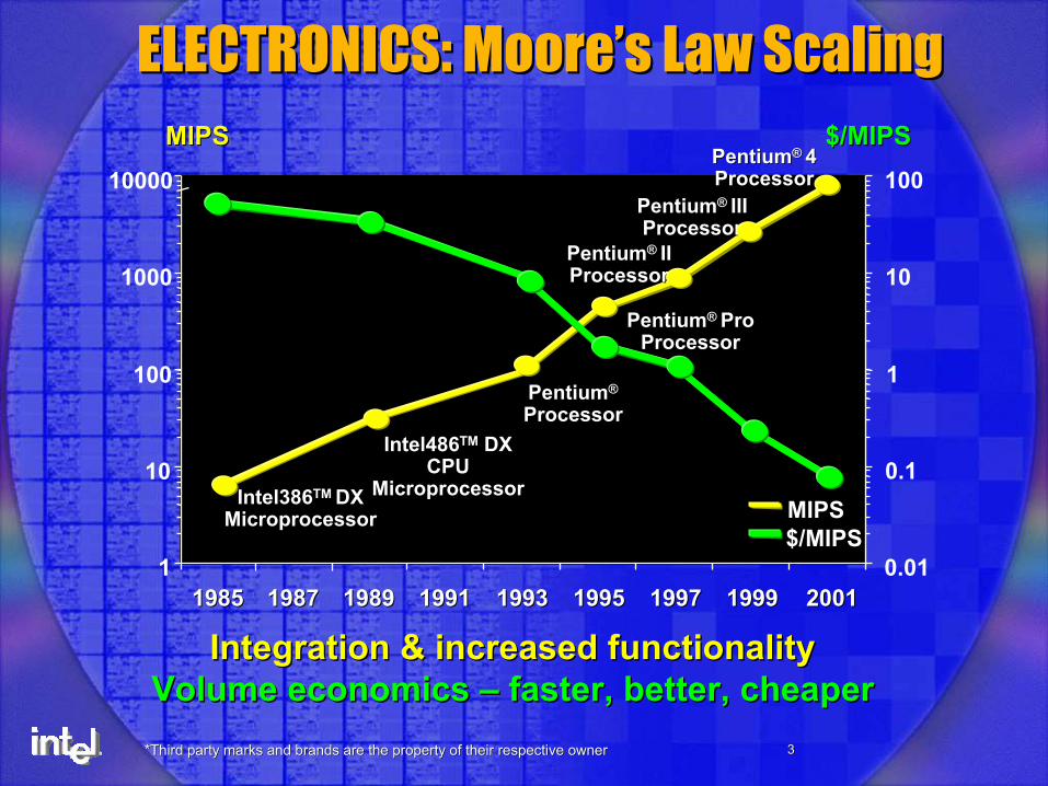
ELECTRONICS: ELECTRONICS: MooreMoore’’ss Law ScalingLaw ScalingMIPSMIPS
PentiumPentium®®
ProcessorProcessor
PentiumPentium®® ProProProcessorProcessor
PentiumPentium®® IIIIProcessorProcessor
PentiumPentium®® IIIIIIProcessorProcessor
PentiumPentium®® 44ProcessorProcessor
Intel386Intel386TM TM DXDXMicroprocessorMicroprocessor
Intel486Intel486TMTM DX DX CPU CPU
MicroprocessorMicroprocessor
1
10
100
1000
10000
19851985 19891989 19931993 19951995 19971997 19991999 20012001
MIPS
$/MIPS$/MIPS
0.01
0.1
1
10
100
$/MIPS
1991199119871987
Volume economics Volume economics –– faster, better, cheaper faster, better, cheaper Integration & increased functionality Integration & increased functionality
*Third party marks and brands are the property of their respecti*Third party marks and brands are the property of their respective ownerve owner 44
Industry standard silicon manufacturing processes could Industry standard silicon manufacturing processes could enable integration, bring volume economics to optical.enable integration, bring volume economics to optical.
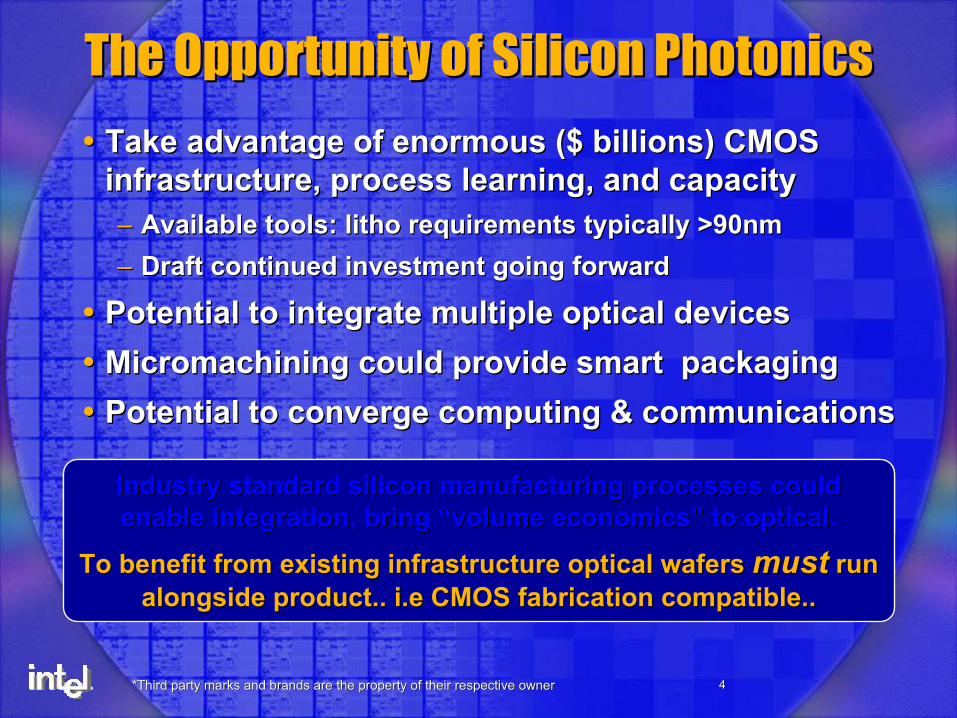
The Opportunity of Silicon PhotonicsThe Opportunity of Silicon Photonics
Take advantage of enormous ($ billions) CMOS Take advantage of enormous ($ billions) CMOS infrastructure, process learning, and capacity infrastructure, process learning, and capacity –– Available tools: litho requirements typically >90nm Available tools: litho requirements typically >90nm –– Draft continued investment going forwardDraft continued investment going forward
Potential to integrate multiple optical devices Potential to integrate multiple optical devices Micromachining could provide smart packagingMicromachining could provide smart packagingPotential to converge computing & communicationsPotential to converge computing & communications
Industry standard silicon manufacturing processes could Industry standard silicon manufacturing processes could enable integration, bring enable integration, bring ““volume economicsvolume economics”” to optical.to optical.
To benefit from existing infrastructure optical wafers To benefit from existing infrastructure optical wafers mustmust run run alongside product.. alongside product.. i.ei.e CMOS fabrication compatible..CMOS fabrication compatible..
*Third party marks and brands are the property of their respecti*Third party marks and brands are the property of their respective ownerve owner 55
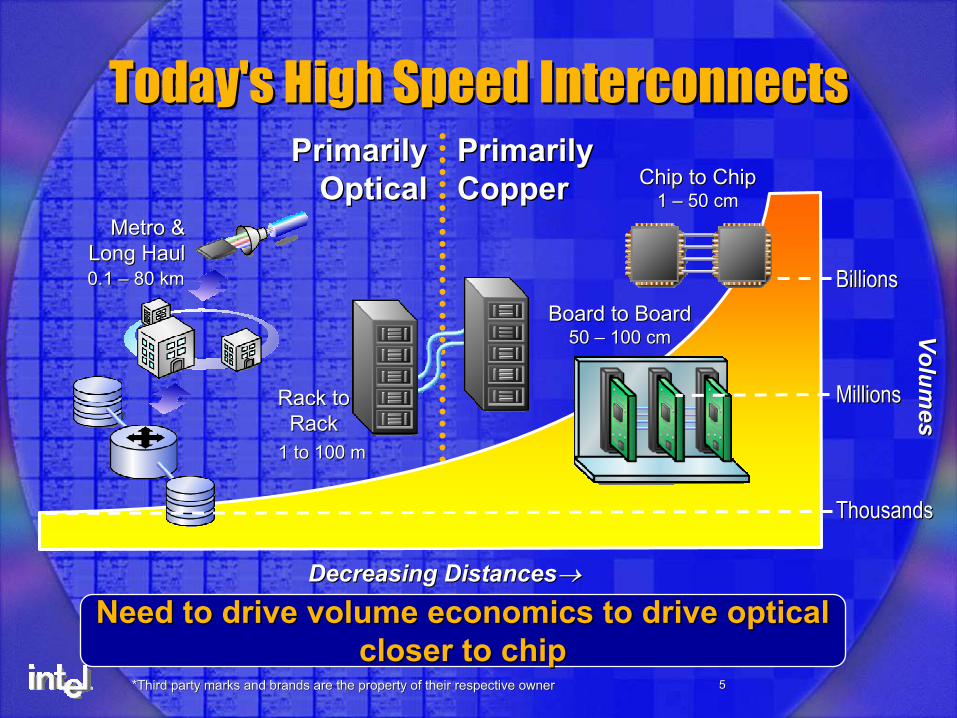
Today's High Speed InterconnectsToday's High Speed Interconnects
Chip to ChipChip to Chip1 1 –– 50 cm50 cm
Board to BoardBoard to Board50 50 –– 100 cm100 cm
1 to 100 m1 to 100 m
Rack to Rack to RackRack
0.1 0.1 –– 80 km80 km
Metro &Metro &Long HaulLong Haul
Decreasing DistancesDecreasing Distances→→
PrimarilyPrimarilyOpticalOptical
Primarily Primarily CopperCopper
Need to drive volume economics to drive optical Need to drive volume economics to drive optical closer to chipcloser to chip
BillionsBillions
MillionsMillions
ThousandsThousands
Volumes
Volumes
*Third party marks and brands are the property of their respecti*Third party marks and brands are the property of their respective ownerve owner 66
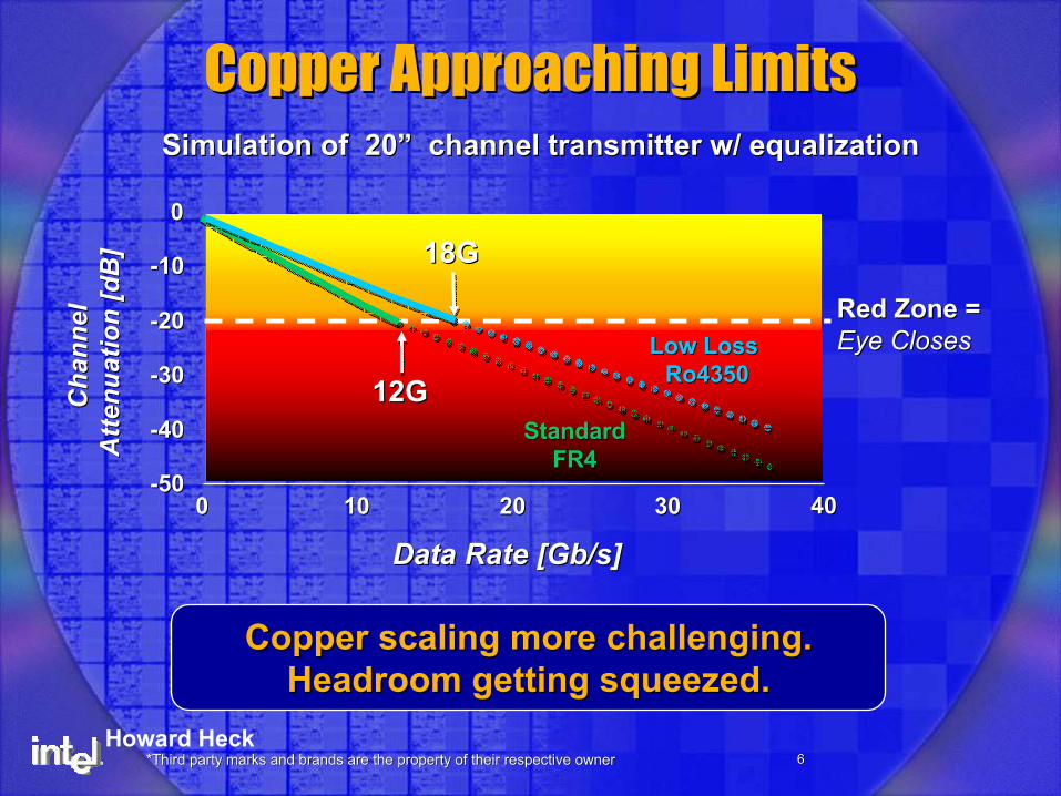
Copper Approaching LimitsCopper Approaching Limits
Data Rate [Gb/s]Data Rate [Gb/s]
StandardStandardFR4FR4
--5050
--4040
--3030
--2020
--1010
00
00 1010 2020 3030
Cha
nnel
C
hann
el
Atte
nuat
ion
[dB
]A
ttenu
atio
n [d
B]
12G12G
Red Zone =Red Zone =Eye ClosesEye Closes
4040
Simulation of 20Simulation of 20”” channel transmitter w/ equalizationchannel transmitter w/ equalization
Copper scaling more challenging.Copper scaling more challenging.Headroom getting squeezed.Headroom getting squeezed.
Low LossLow LossRo4350Ro4350
18G18G
Howard Heck
*Third party marks and brands are the property of their respecti*Third party marks and brands are the property of their respective ownerve owner 77
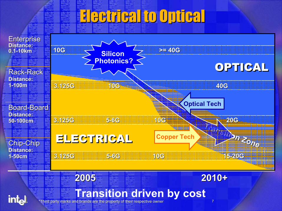
2010+2010+20052005
ChipChip--ChipChipDistance: Distance: 11--50cm50cm
BoardBoard--BoardBoardDistance: Distance: 5050--100cm100cm
RackRack--RackRackDistance: Distance: 11--100m100m
EnterpriseEnterpriseDistance:Distance:0.10.1--10km10km
OPTICALOPTICAL
Electrical to Optical Electrical to Optical
ELECTRICALELECTRICAL
3.125G 10G 3.125G 10G 40G40G
3.125G 53.125G 5--6G6G 10G10G 20G20G
3.125G 53.125G 5--6G6G 10G10G 1515--20G20G
10G 10G >= 40G>= 40G
Copper TechTransition Zone
Transition Zone
Silicon Photonics?
Optical Tech
Transition driven by cost
*Third party marks and brands are the property of their respecti*Third party marks and brands are the property of their respective ownerve owner 88
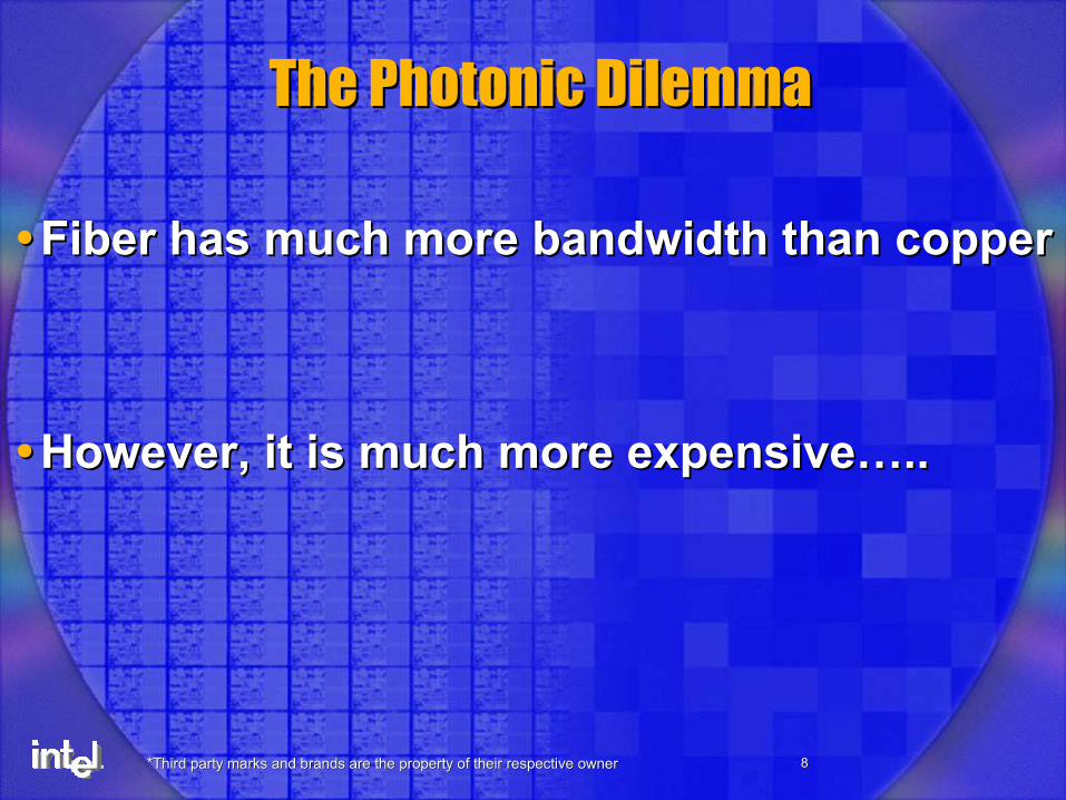
The Photonic DilemmaThe Photonic Dilemma
Fiber has much more bandwidth than copperFiber has much more bandwidth than copper
However, it is much more expensiveHowever, it is much more expensive……....
*Third party marks and brands are the property of their respecti*Third party marks and brands are the property of their respective ownerve owner 99
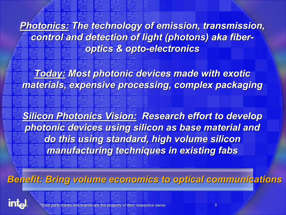
Photonics:Photonics: The technology of emission, transmission, The technology of emission, transmission, control and detection of light (photons) aka fibercontrol and detection of light (photons) aka fiber--
optics & optooptics & opto--electronicselectronics
Today:Today: Most photonic devices made with exotic Most photonic devices made with exotic materials, expensive processing, complex packagingmaterials, expensive processing, complex packaging
Silicon Photonics Vision:Silicon Photonics Vision: Research effort to develop Research effort to develop photonic devices using silicon as base material and photonic devices using silicon as base material and
do this using standard, high volume silicon do this using standard, high volume silicon manufacturing techniques in existing fabsmanufacturing techniques in existing fabs
Benefit: Bring volume economics to optical communicationsBenefit: Bring volume economics to optical communications
*Third party marks and brands are the property of their respecti*Third party marks and brands are the property of their respective ownerve owner 1010
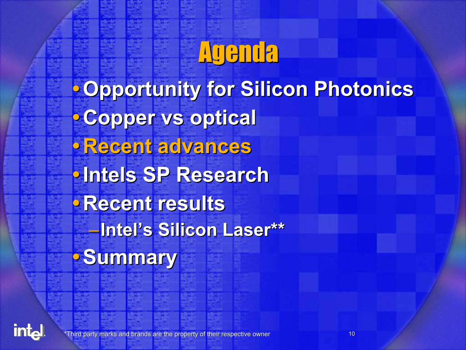
Agenda Agenda Opportunity for Silicon PhotonicsOpportunity for Silicon PhotonicsCopper Copper vsvs optical optical Recent advancesRecent advancesIntelsIntels SP ResearchSP ResearchRecent resultsRecent results–– IntelIntel’’s Silicon Laser**s Silicon Laser**
SummarySummary
*Third party marks and brands are the property of their respecti*Third party marks and brands are the property of their respective ownerve owner 1111
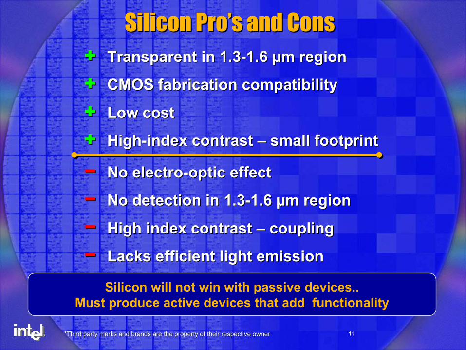
++ Transparent in 1.3Transparent in 1.3--1.6 1.6 µµm regionm region
++ CMOS fabrication compatibility CMOS fabrication compatibility
++ Low costLow cost
++ HighHigh--index contrast index contrast –– small footprintsmall footprint
Silicon ProSilicon Pro’’s and Conss and Cons
−− No electroNo electro--optic effectoptic effect
−− No detection in 1.3No detection in 1.3--1.6 1.6 µµm regionm region
−− High index contrast High index contrast –– coupling coupling
−− Lacks efficient light emission Lacks efficient light emission
Silicon will not win with passive devices.. Must produce active devices that add functionality
*Third party marks and brands are the property of their respecti*Third party marks and brands are the property of their respective ownerve owner 1212
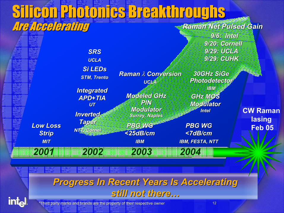
Silicon Silicon PhotonicsPhotonics Breakthroughs Breakthroughs Are AcceleratingAre Accelerating
Low Loss Low Loss StripStrip
MITMIT
2004200320022001
PBG WGPBG WG<25dB/cm<25dB/cm
IBMIBM
Modeled GHz Modeled GHz PIN PIN
ModulatorModulatorSurrey, NaplesSurrey, Naples
Raman Raman λ λ ConversionConversionUCLAUCLA
Progress In Recent Years Is Accelerating Progress In Recent Years Is Accelerating still not therestill not there……
Raman Net Pulsed GainRaman Net Pulsed Gain9/6: Intel9/6: Intel
9/20: Cornell9/20: Cornell9/29: UCLA 9/29: UCLA 9/29: CUHK9/29: CUHK
GHz MOS GHz MOS ModulatorModulator
IntelIntel
PBG WGPBG WG<7dB/cm<7dB/cm
IBM, FESTA, NTTIBM, FESTA, NTT
30GHz 30GHz SiGeSiGePhotodetectorPhotodetector
IBMIBM
SRS SRS UCLAUCLA
SiSi LEDsLEDsSTM, STM, TrentoTrento
IntegratedIntegratedAPD+TIAAPD+TIA
UTUT
Inverted Inverted TaperTaper
NTT, CornelNTT, Cornel
CW Raman lasing Feb 05
*Third party marks and brands are the property of their respecti*Third party marks and brands are the property of their respective ownerve owner 1313
Agenda Agenda Opportunity for Silicon PhotonicsOpportunity for Silicon PhotonicsCopper Copper vsvs optical optical Recent advancesRecent advancesIntelIntel’’s SP Researchs SP ResearchRecent resultsRecent results–– IntelIntel’’s Silicon Laser**s Silicon Laser**
SummarySummary
*Third party marks and brands are the property of their respecti*Third party marks and brands are the property of their respective ownerve owner 1414
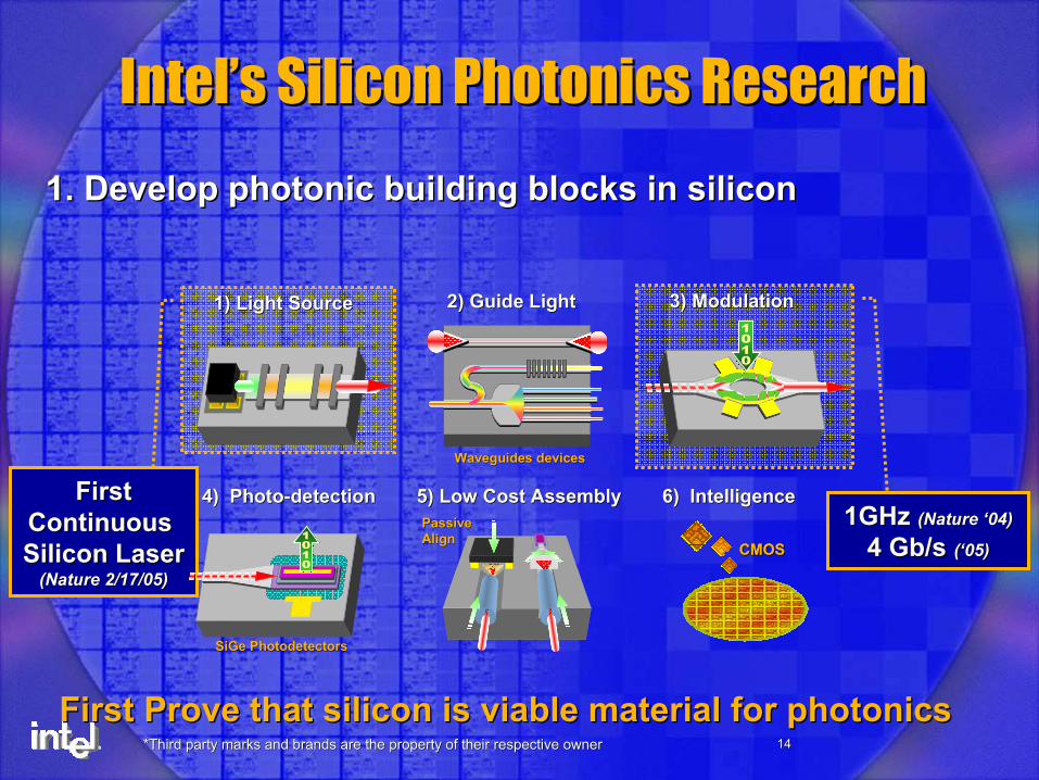
FirstFirstContinuous Continuous Silicon LaserSilicon Laser
(Nature 2/17/05)(Nature 2/17/05)
1GHz 1GHz (Nature (Nature ‘‘04)04)
4 Gb/s 4 Gb/s ((‘‘05)05)
1) Light Source1) Light Source
4) Photo4) Photo--detectiondetection
3) Modulation3) Modulation2) Guide Light2) Guide Light
6) Intelligence6) Intelligence5) Low Cost Assembly5) Low Cost AssemblyPassive Passive AlignAlign
CMOSCMOSCMOSCMOS
Mirror
Waveguides devicesWaveguides devices
SiGeSiGe PhotodetectorsPhotodetectors
IntelIntel’’s Silicon Photonics Researchs Silicon Photonics Research
1. Develop photonic building blocks in silicon1. Develop photonic building blocks in silicon
First Prove that silicon is viable material for photonicsFirst Prove that silicon is viable material for photonics
*Third party marks and brands are the property of their respecti*Third party marks and brands are the property of their respective ownerve owner 1515
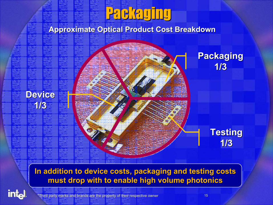
PackagingPackaging
DeviceDevice1/31/3
PackagingPackaging1/31/3
TestingTesting1/31/3
In addition to device costs, packaging and testing costs In addition to device costs, packaging and testing costs must drop with to enable high volume photonicsmust drop with to enable high volume photonics
Approximate Optical Product Cost BreakdownApproximate Optical Product Cost Breakdown
*Third party marks and brands are the property of their respecti*Third party marks and brands are the property of their respective ownerve owner 1616
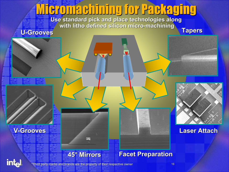
Micromachining for PackagingMicromachining for PackagingUse standard pick and place technologies alongUse standard pick and place technologies along
with litho defined silicon microwith litho defined silicon micro--machiningmachining
VV--GroovesGrooves
UU--GroovesGrooves
4545°° MirrorsMirrors
TapersTapers
Laser AttachLaser Attach
Facet PreparationFacet Preparation
MirrorMirror
*Third party marks and brands are the property of their respecti*Third party marks and brands are the property of their respective ownerve owner 1717
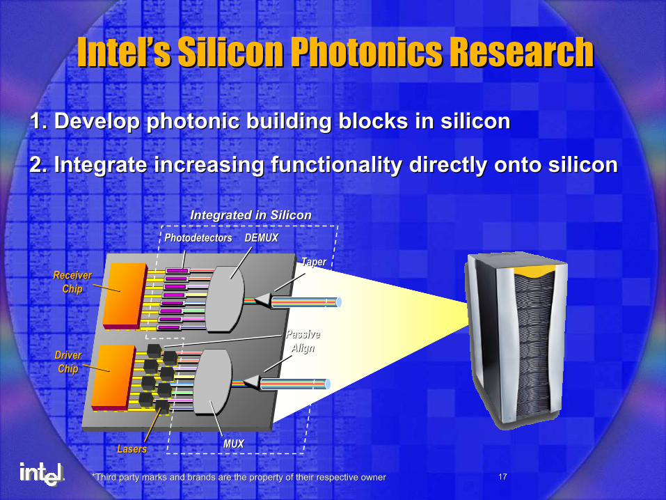
IntelIntel’’s Silicon Photonics Researchs Silicon Photonics Research
1. Develop photonic building blocks in silicon1. Develop photonic building blocks in silicon
2. Integrate increasing functionality directly onto silicon 2. Integrate increasing functionality directly onto silicon
DEMUXDEMUX
MUXMUX
DriverDriverChipChip
ReceiverReceiverChipChip
LasersLasers
PhotodetectorsPhotodetectors
TaperTaper
PassivePassiveAlignAlign
Integrated in SiliconIntegrated in Silicon
*Third party marks and brands are the property of their respecti*Third party marks and brands are the property of their respective ownerve owner 1818
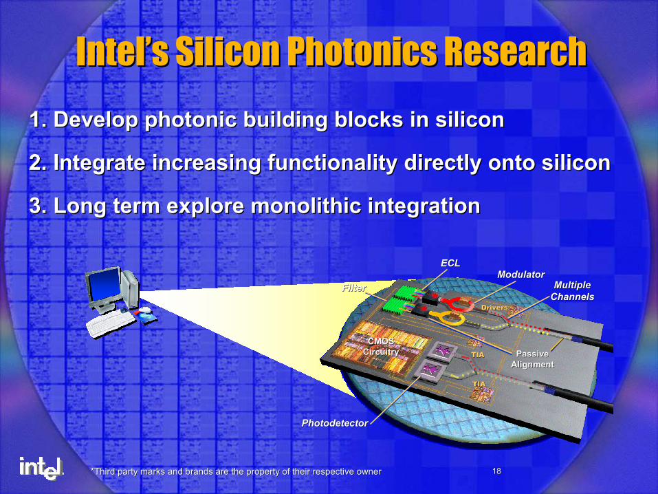
IntelIntel’’s Silicon Photonics Researchs Silicon Photonics Research
1. Develop photonic building blocks in silicon1. Develop photonic building blocks in silicon
2. Integrate increasing functionality directly onto silicon 2. Integrate increasing functionality directly onto silicon
3. Long term explore monolithic integration3. Long term explore monolithic integration
TIATIA
TIATIA
DriversDrivers
TIATIA
TIATIA
DriversDrivers
CMOSCMOSCircuitryCircuitry
PhotodetectorPhotodetector
PassivePassiveAlignmentAlignment
ModulatorModulatorECLECL
FilterFilter MultipleMultipleChannelsChannels
*Third party marks and brands are the property of their respecti*Third party marks and brands are the property of their respective ownerve owner 1919
SILICON LASERSILICON LASERWhat we announced on Feb 17What we announced on Feb 17thth
*Third party marks and brands are the property of their respecti*Third party marks and brands are the property of their respective ownerve owner 2020
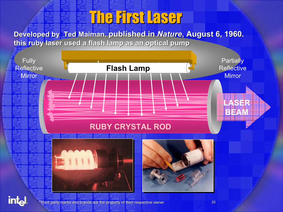
The First LaserThe First Laser
FullyReflective
Mirror
PartiallyReflective
Mirror
Developed by Ted Developed by Ted MaimanMaiman, , published in published in NatureNature, August 6, 1960., August 6, 1960.this ruby laser used a flash lamp as an optical pump this ruby laser used a flash lamp as an optical pump
RUBY CRYSTAL ROD
LASERBEAM
Flash Lamp
*Third party marks and brands are the property of their respecti*Third party marks and brands are the property of their respective ownerve owner 2121
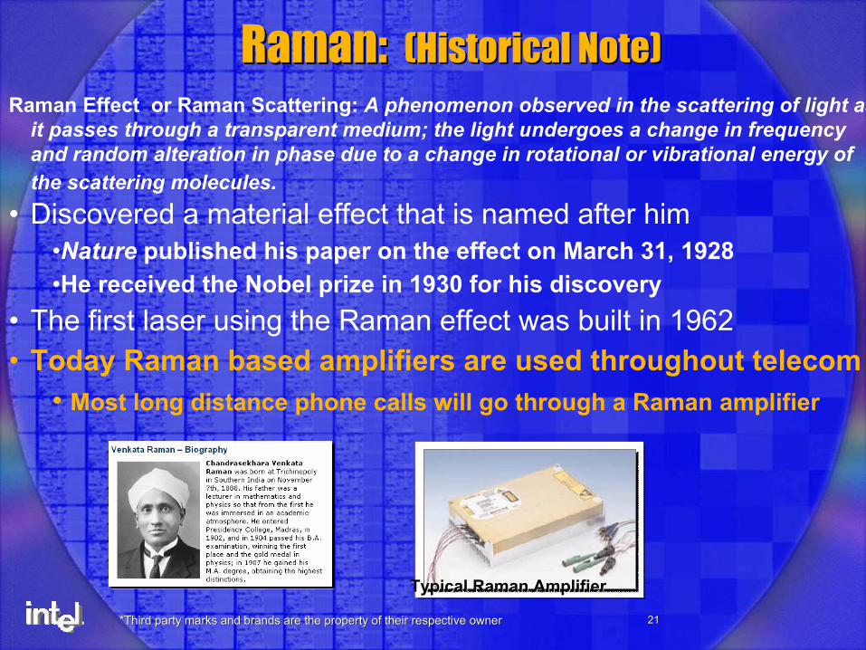
Raman: Raman: (Historical Note)(Historical Note)Raman Effect or Raman Scattering: A phenomenon observed in the scattering of light as
it passes through a transparent medium; the light undergoes a change in frequency and random alteration in phase due to a change in rotational or vibrational energy of the scattering molecules.
• Discovered a material effect that is named after him•Nature published his paper on the effect on March 31, 1928•He received the Nobel prize in 1930 for his discovery
• The first laser using the Raman effect was built in 1962• Today Raman based amplifiers are used throughout telecom
• Most long distance phone calls will go through a Raman amplifier
Typical Raman AmplifierTypical Raman Amplifier
*Third party marks and brands are the property of their respecti*Third party marks and brands are the property of their respective ownerve owner 2222
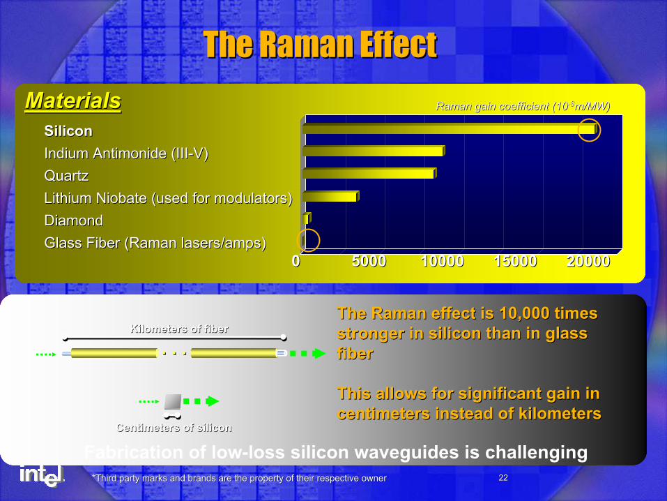
The Raman EffectThe Raman Effect
00 100001000050005000 1500015000 2000020000Glass Fiber (Raman lasers/amps)Glass Fiber (Raman lasers/amps)DiamondDiamondLithium Niobate (used for modulators) Lithium Niobate (used for modulators) QuartzQuartzIndium Indium AntimonideAntimonide (III(III--V)V)SiliconSilicon
MaterialsMaterials Raman gain coefficient (10Raman gain coefficient (10--88m/MW)m/MW)
The Raman effect is 10,000 times The Raman effect is 10,000 times stronger in silicon than in glass stronger in silicon than in glass fiberfiber
This allows for significant gain in This allows for significant gain in centimeters instead of kilometerscentimeters instead of kilometers
Kilometers of fiberKilometers of fiber
Centimeters of siliconCentimeters of silicon
. . .. . .
Fabrication of low-loss silicon waveguides is challenging

*Third party marks and brands are the property of their respecti*Third party marks and brands are the property of their respective ownerve owner 2323
Raman Gain in SiliconGain in Silicon
0 200 400 600 800 10000.0
0.5
1.0
1.5
2.0
2.5
(b)
Ram
an g
ain
(dB
)
Input pump power(mW)
Raman Gain and WG loss vs. Input Pump Power
0
0.5
1
1.5
2
2.5
3
3.5
0 200 400 600Pump Power (mW)
Ram
an G
ain/
WG
Los
s (d
B)
-1.6
-1.4
-1.2
-1
-0.8
-0.6
-0.4
-0.2
Gai
n-Lo
ss (d
B)
Raman GainWG LossLoss w/o PumpGain-Loss
CW Gain Saturation due to TPA induced FCA
Silicon Waveguide
Pump in
Probe in
Pump out
Probe out
Silicon Waveguide
Pump in
Probe in
Pump out
Probe out
Pump/probe experiment
*Third party marks and brands are the property of their respecti*Third party marks and brands are the property of their respective ownerve owner 2424
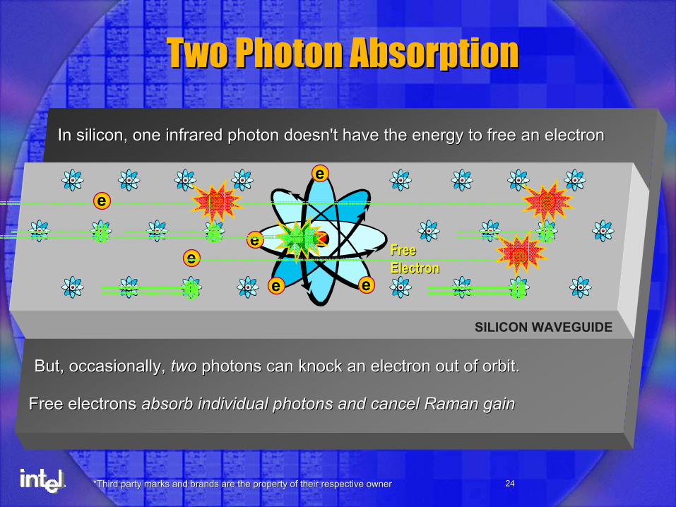
Two Photon AbsorptionTwo Photon Absorption
e
ee
e Free Free ElectronElectron
In silicon, one infrared photon doesn't have the energy to free In silicon, one infrared photon doesn't have the energy to free an electronan electron
But, occasionally, But, occasionally, twotwo photons can knock an electron out of orbit.photons can knock an electron out of orbit.
Free electrons Free electrons absorb individual photons and cancel Raman gainabsorb individual photons and cancel Raman gain
e
SILICON WAVEGUIDE
e
e e
e
*Third party marks and brands are the property of their respecti*Third party marks and brands are the property of their respective ownerve owner 2525
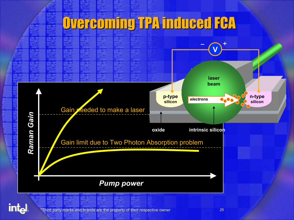
Overcoming TPA induced FCAOvercoming TPA induced FCA
Pump power
Ram
an G
ain
Gain limit due to Two Photon Absorption problem
p-typesilicon
n-typesilicon
V+−
laser beam
electrons
intrinsic siliconoxide
Gain needed to make a laser
*Third party marks and brands are the property of their respecti*Third party marks and brands are the property of their respective ownerve owner 2626
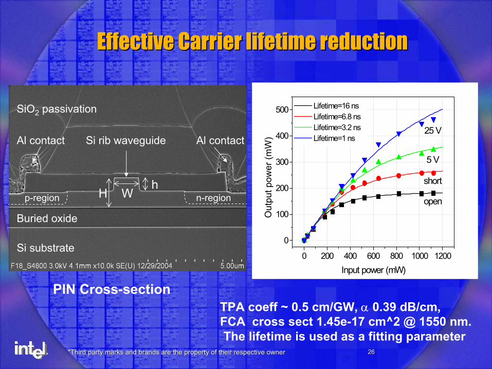
Effective Carrier lifetime reductionEffective Carrier lifetime reduction
0 200 400 600 800 1000 1200
0
100
200
300
400
500
25 V
5 V
short
open
Out
put p
ower
(mW
)Input power (mW)
Lifetime=16 ns Lifetime=6.8 ns Lifetime=3.2 ns Lifetime=1 ns
SiO2 passivation
Si rib waveguide
Si substrate
Buried oxide
p-region n-region
Al contact Al contact
H Wh
PIN Cross-sectionTPA coeff ~ 0.5 cm/GW, α 0.39 dB/cm, FCA cross sect 1.45e-17 cm^2 @ 1550 nm.The lifetime is used as a fitting parameter
*Third party marks and brands are the property of their respecti*Third party marks and brands are the property of their respective ownerve owner 2727
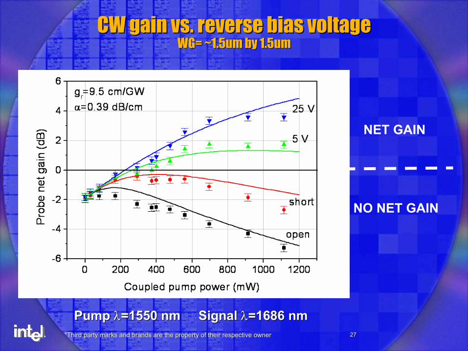
CW gain vs. reverse bias voltageCW gain vs. reverse bias voltageWG= ~1.5um by 1.5umWG= ~1.5um by 1.5um
NO NET GAIN
NET GAIN
Pump Pump λλ=1550 nm Signal =1550 nm Signal λλ=1686 nm=1686 nm
*Third party marks and brands are the property of their respecti*Third party marks and brands are the property of their respective ownerve owner 2828
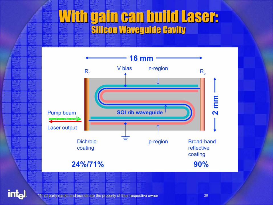
With gain can build Laser: With gain can build Laser: Silicon Waveguide CavitySilicon Waveguide Cavity
Laser output
Pump beam SOI rib waveguide
Rf Rb
p-region
n-regionV bias
Dichroiccoating
Broad-bandreflectivecoating
16 mm
2 m
m
24%/71% 90%
*Third party marks and brands are the property of their respecti*Third party marks and brands are the property of their respective ownerve owner 2929
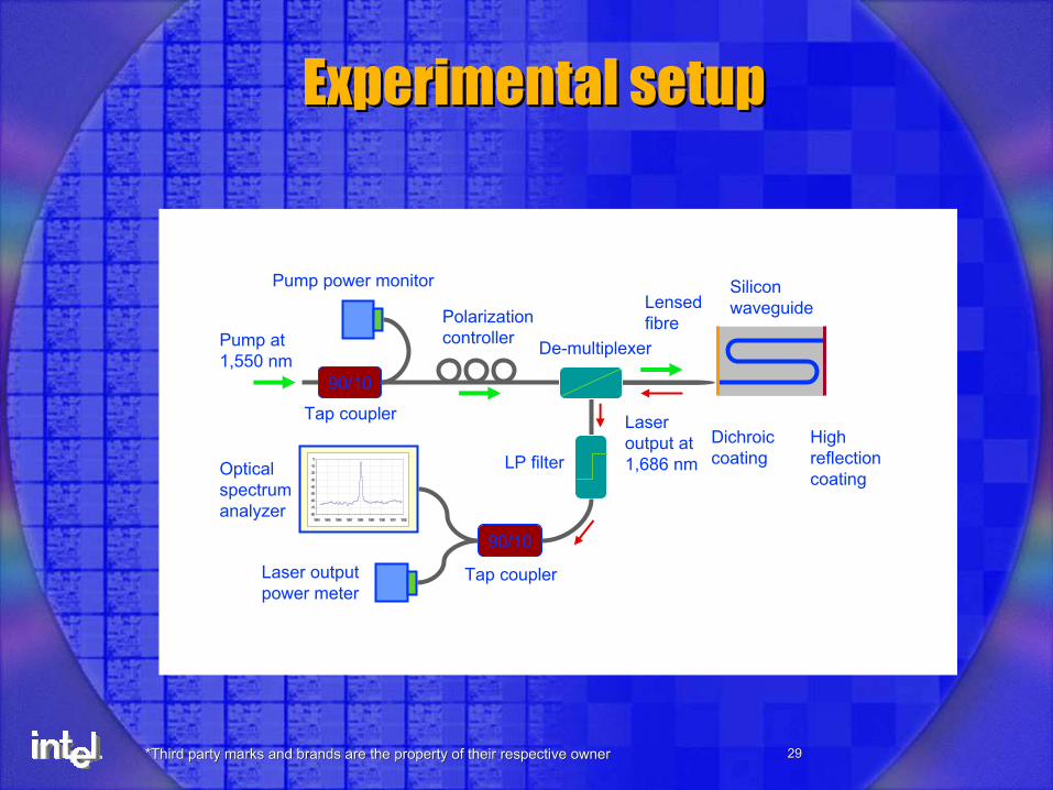
Experimental setupExperimental setup
Pump at1,550 nm
High reflectioncoating
Siliconwaveguide
Laseroutput at 1,686 nm
Laser output power meter
Opticalspectrumanalyzer -80
-70
-60
-50
-40
-30
-20
-10
0
1684 1685 1686 1687 1688 1689 1690 1691 1692
Dichroiccoating
De-multiplexer
90/10
Pump power monitor
Polarization controller
90/10
Tap coupler
LP filter
Tap coupler
Lensedfibre
*Third party marks and brands are the property of their respecti*Third party marks and brands are the property of their respective ownerve owner 3030
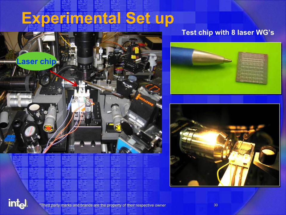
Laser chip
Experimental Set upTest chip with 8 laser WG’s
*Third party marks and brands are the property of their respecti*Third party marks and brands are the property of their respective ownerve owner 3131
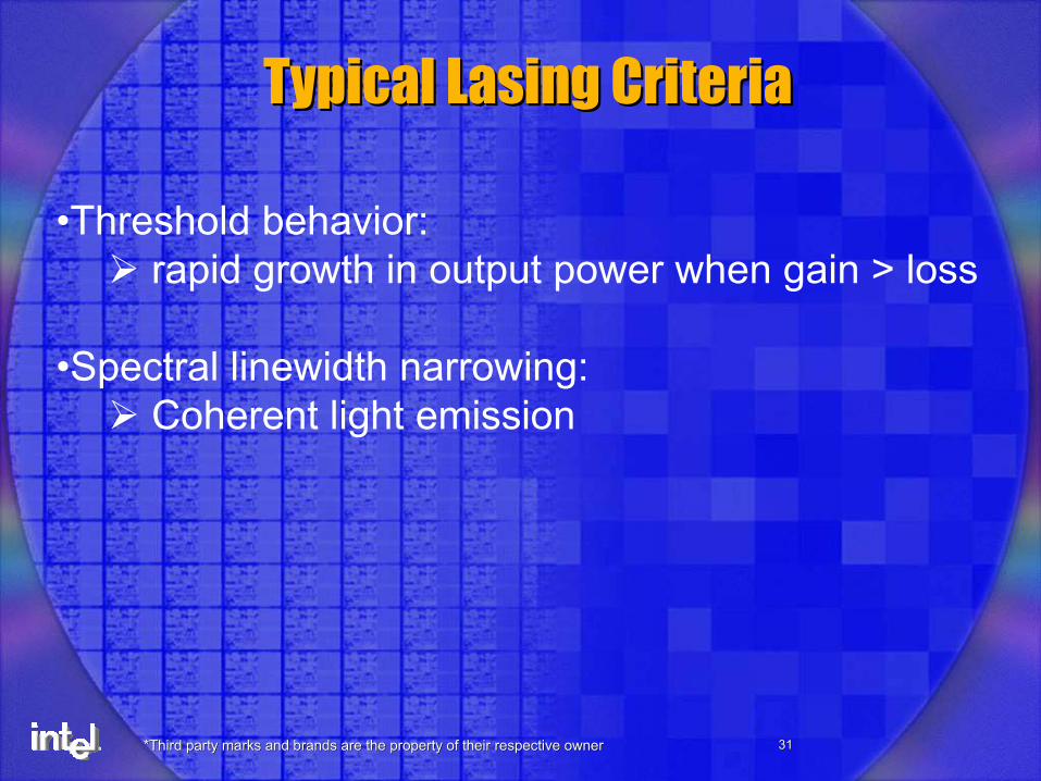
Typical Lasing CriteriaTypical Lasing Criteria
•Threshold behavior:rapid growth in output power when gain > loss
•Spectral linewidth narrowing: Coherent light emission
*Third party marks and brands are the property of their respecti*Third party marks and brands are the property of their respective ownerve owner 3232
0.0
1.0
2.0
3.0
4.0
5.0
6.0
7.0
8.0
9.0
10.0
0 200 400 600 800
Coupled pump power (mW)
Lase
r out
put (
mW
)25V bias5V bias25V slope5V slope
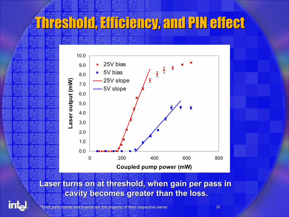
Threshold, Efficiency, and PIN effectThreshold, Efficiency, and PIN effect
Laser turns on at threshold, when gain per pass in Laser turns on at threshold, when gain per pass in cavity becomes greater than the loss.cavity becomes greater than the loss.
*Third party marks and brands are the property of their respecti*Third party marks and brands are the property of their respective ownerve owner 3333
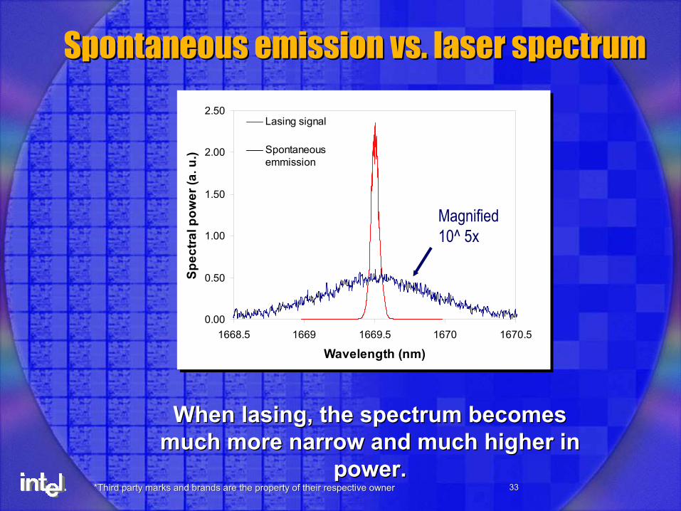
Spontaneous emission vs. laser spectrumSpontaneous emission vs. laser spectrum
When lasing, the spectrum becomes When lasing, the spectrum becomes much more narrow and much higher in much more narrow and much higher in
power.power.
0.00
0.50
1.00
1.50
2.00
2.50
1668.5 1669 1669.5 1670 1670.5
Wavelength (nm)
Spec
tral p
ower
(a. u
.)
Lasing signal
Spontaneousemmission
0.00
0.50
1.00
1.50
2.00
2.50
1668.5 1669 1669.5 1670 1670.5
Wavelength (nm)
Spec
tral p
ower
(a. u
.)
Lasing signal
Spontaneousemmission
Magnified10^ 5x
*Third party marks and brands are the property of their respecti*Third party marks and brands are the property of their respective ownerve owner 3434
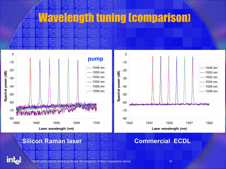
Wavelength tuning (comparison))
-80
-70
-60
-50
-40
-30
-20
-10
0
1680 1685 1690 1695 1700
Laser wavelength (nm)
Spac
tral
pow
er (d
B)
1548 nm1550 nm1552 nm1554 nm1556 nm1558 nm
Silicon Raman laser Commercial ECDL
-80
-70
-60
-50
-40
-30
-20
-10
0
1542 1547 1552 1557 1562
Laser wavelength (nm)
Spac
tral
pow
er (d
B)
1548 nm1550 nm1552 nm1554 nm1556 nm1558 nm
pump
*Third party marks and brands are the property of their respecti*Third party marks and brands are the property of their respective ownerve owner 3535
Potential ApplicationsPotential Applications
*Third party marks and brands are the property of their respecti*Third party marks and brands are the property of their respective ownerve owner 3636
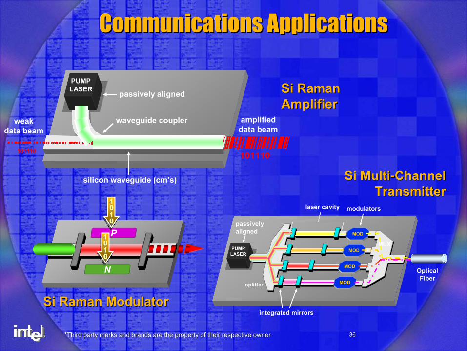
Communications ApplicationsCommunications Applications
PUMPLASER passively aligned
amplifieddata beam
silicon waveguide (cm’s)
101110 101110
waveguide couplerweakdata beam
SiSi RamanRamanAmplifierAmplifier
PUMPLASER
MOD
MOD
MOD
MOD
modulators
passively aligned
laser cavity
splitter
OpticalFiber
MUX
integrated mirrors
SiSi MultiMulti--ChannelChannelTransmitterTransmitter
N
P
SiSi Raman ModulatorRaman Modulator
*Third party marks and brands are the property of their respecti*Third party marks and brands are the property of their respective ownerve owner 3737
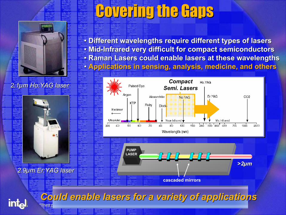
Covering the Gaps Covering the Gaps
2.12.1µµm m Ho:YAGHo:YAG laserlaser
PUMPLASER
cascaded mirrors
•• Different wavelengths require different types of lasersDifferent wavelengths require different types of lasers•• MidMid--Infrared very difficult for compact semiconductorsInfrared very difficult for compact semiconductors•• Raman Lasers could enable lasers at these wavelengths Raman Lasers could enable lasers at these wavelengths •• Applications in sensing, analysis, medicine,Applications in sensing, analysis, medicine, and othersand others
CompactCompactSemi. LasersSemi. Lasers
Could enable lasers for a variety of applicationsCould enable lasers for a variety of applications
>2>2µµmm2.92.9µµm m Er:YAGEr:YAG laserlaser
*Third party marks and brands are the property of their respecti*Third party marks and brands are the property of their respective ownerve owner 3838
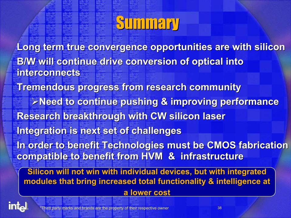
Silicon will not win with individual devices, but with integrateSilicon will not win with individual devices, but with integrated d modules that bring increased total functionality & intelligence modules that bring increased total functionality & intelligence at at
a lower costa lower cost
SummarySummaryLong term true convergence opportunities are with siliconLong term true convergence opportunities are with siliconB/W will continue drive conversion of optical into B/W will continue drive conversion of optical into interconnectsinterconnectsTremendous progress from research communityTremendous progress from research community
Need to continue pushing & improving performanceNeed to continue pushing & improving performanceResearch breakthrough with CW silicon laserResearch breakthrough with CW silicon laserIntegration is next set of challengesIntegration is next set of challengesIn order to benefit Technologies must be CMOS fabrication In order to benefit Technologies must be CMOS fabrication compatible to benefit from HVM & infrastructurecompatible to benefit from HVM & infrastructure
*Third party marks and brands are the property of their respecti*Third party marks and brands are the property of their respective ownerve owner 3939
BACKUP
*Third party marks and brands are the property of their respecti*Third party marks and brands are the property of their respective ownerve owner 4040
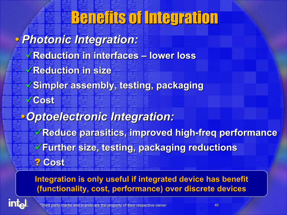
Photonic Integration:Photonic Integration:Reduction in interfaces Reduction in interfaces –– lower losslower lossReduction in sizeReduction in sizeSimpler assembly, testing, packagingSimpler assembly, testing, packagingCostCost
Benefits of IntegrationBenefits of Integration
Optoelectronic IntegrationOptoelectronic Integration::Reduce Reduce parasiticsparasitics, improved high, improved high--freq performancefreq performanceFurther size, testing, packaging reductions Further size, testing, packaging reductions
?? CostCostIntegration is only useful if integrated device has benefit (functionality, cost, performance) over discrete devices
*Third party marks and brands are the property of their respecti*Third party marks and brands are the property of their respective ownerve owner 4141
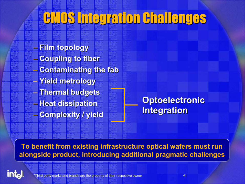
CMOS Integration ChallengesCMOS Integration Challenges
–– Film topologyFilm topology–– Coupling to fiberCoupling to fiber–– Contaminating the Contaminating the fabfab–– Yield metrologyYield metrology–– Thermal budgetsThermal budgets–– Heat dissipationHeat dissipation–– Complexity / yieldComplexity / yield
OptoelectronicOptoelectronicIntegrationIntegration
To benefit from existing infrastructure optical wafers must run alongside product, introducing additional pragmatic challenges
*Third party marks and brands are the property of their respecti*Third party marks and brands are the property of their respective ownerve owner 4242
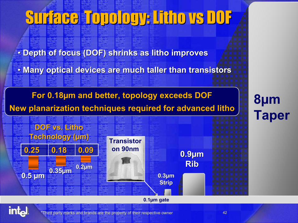
Transistoron 90nm
Surface Topology: Litho Surface Topology: Litho vsvs DOFDOF
0.090.090.180.180.250.25
0.5 0.5 µµmm 0.350.35µµmm 0.20.2µµmm
DOF vs. LithoDOF vs. LithoTechnology (Technology (µµm)m)
For 0.18For 0.18µµm and better, topology exceeds DOFm and better, topology exceeds DOFNew New planarizationplanarization techniques required for advanced lithotechniques required for advanced litho
0.1µm gate
0.30.3µµmmStripStrip
0.90.9µµmmRibRib
8µmTaper
•• Depth of focus (DOF) shrinks as litho improves Depth of focus (DOF) shrinks as litho improves
•• Many optical devices are much taller than transistorsMany optical devices are much taller than transistors
*Third party marks and brands are the property of their respecti*Third party marks and brands are the property of their respective ownerve owner 4343
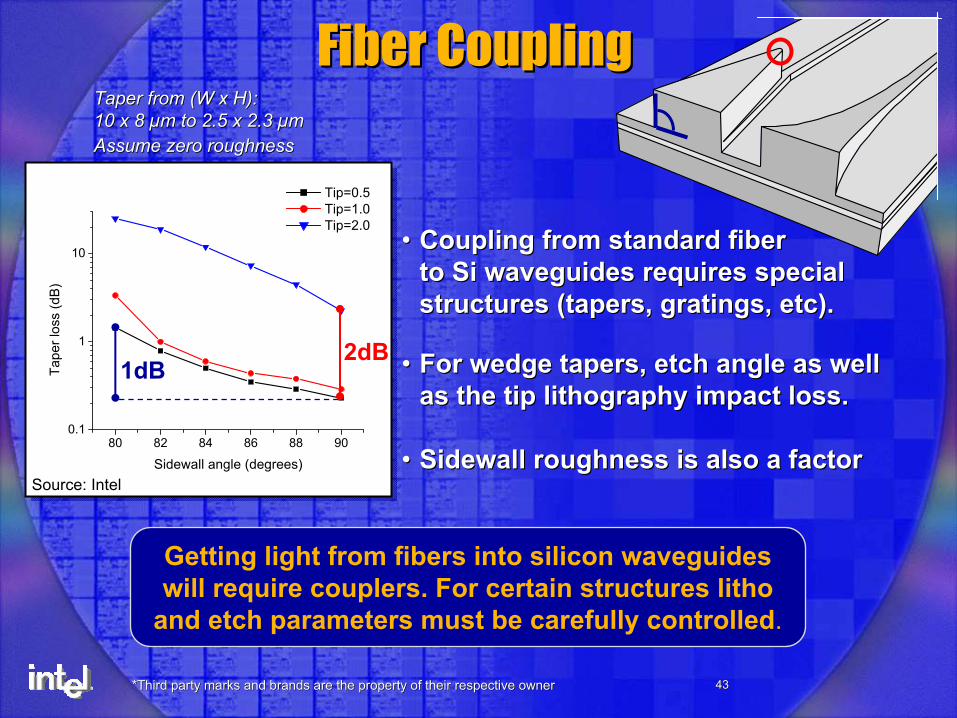
Fiber Coupling Fiber Coupling
Getting light from fibers into silicon waveguides will require couplers. For certain structures litho
and etch parameters must be carefully controlled.
Taper from (W x H): Taper from (W x H): 10 x 8 10 x 8 µµm to 2.5 x 2.3 m to 2.5 x 2.3 µµmmAssume zero roughnessAssume zero roughness
80 82 84 86 88 900.1
1
10
Tape
r los
s (d
B)
Sidewall angle (degrees)
Tip=0.5 Tip=1.0 Tip=2.0
•• Coupling from standard fiber Coupling from standard fiber to to SiSi waveguides requires special waveguides requires special structures (tapers, gratings, etc).structures (tapers, gratings, etc).
2dB1dB
Source: IntelSource: Intel
•• For wedge tapers, etch angle as well For wedge tapers, etch angle as well as the tip lithography impact loss. as the tip lithography impact loss.
•• Sidewall roughness is also a factor Sidewall roughness is also a factor
*Third party marks and brands are the property of their respecti*Third party marks and brands are the property of their respective ownerve owner 4444
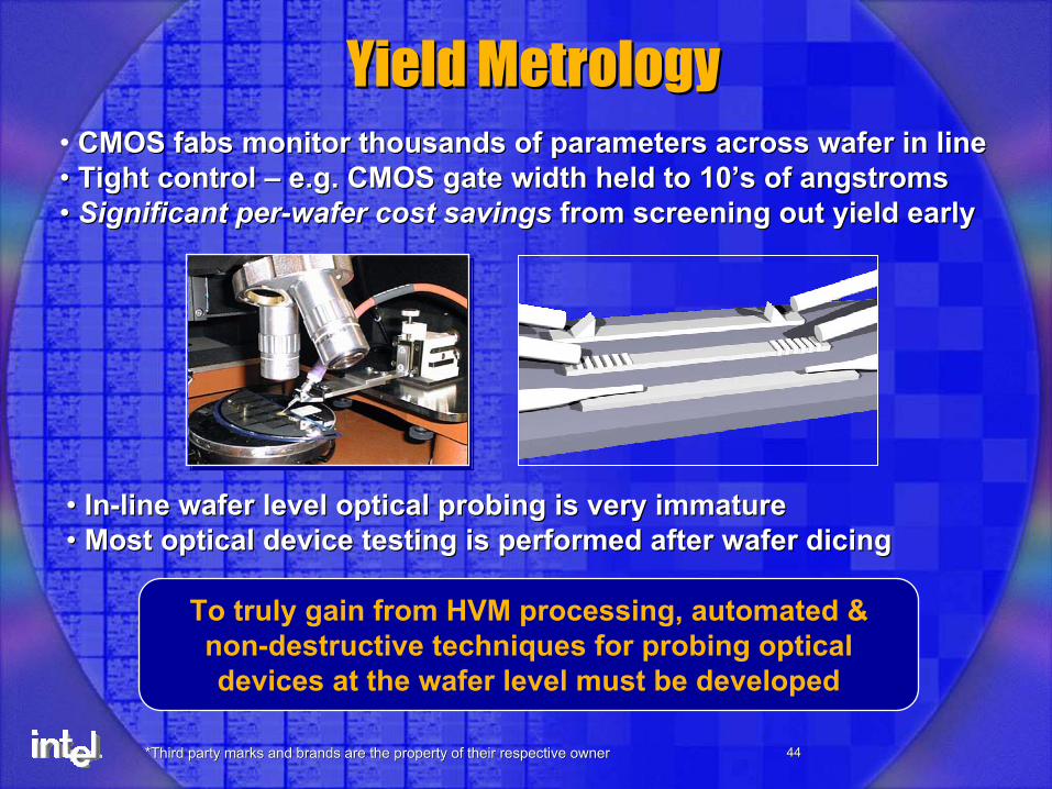
To truly gain from HVM processing, automated & non-destructive techniques for probing optical devices at the wafer level must be developed
• CMOS CMOS fabsfabs monitor thousands of parameters across wafer in line monitor thousands of parameters across wafer in line •• Tight control Tight control –– e.g. CMOS gate width held to 10e.g. CMOS gate width held to 10’’s of angstromss of angstroms•• Significant perSignificant per--wafer cost savingswafer cost savings from screening out yield early from screening out yield early
Yield MetrologyYield Metrology
•• InIn--line wafer level optical probing is very immature line wafer level optical probing is very immature •• Most optical device testing is performed after wafer dicingMost optical device testing is performed after wafer dicing
*Third party marks and brands are the property of their respecti*Third party marks and brands are the property of their respective ownerve owner 4545
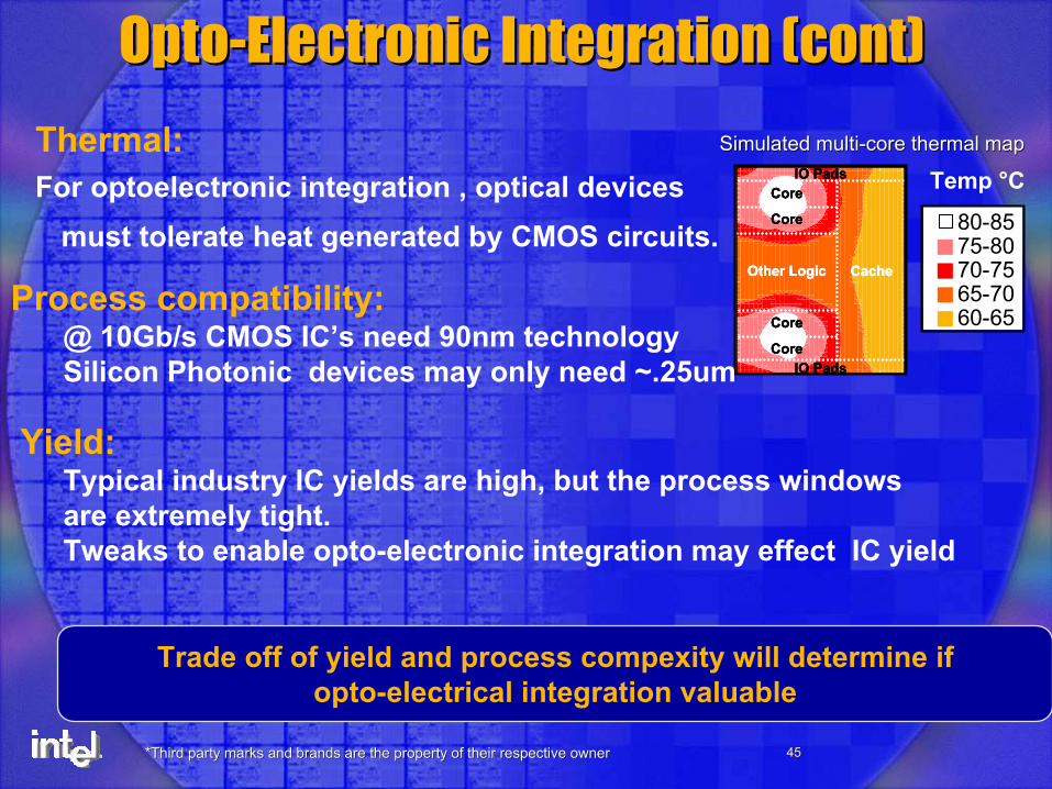
OptoOpto--Electronic Integration (cont)Electronic Integration (cont)
Thermal:For optoelectronic integration , optical devices
must tolerate heat generated by CMOS circuits.Core
Core
Other Logic
Core
Core
Cache
IO Pads
IO Pads
Core
Core
Other Logic
Core
Core
Cache
IO Pads
IO Pads
Core
Core
Other Logic
Core
Core
Cache
IO Pads
IO Pads
80-8575-8070-7565-7060-65
Temp °CSimulated multiSimulated multi--core thermal mapcore thermal map
Process compatibility:@ 10Gb/s CMOS IC’s need 90nm technologySilicon Photonic devices may only need ~.25um
Yield:Typical industry IC yields are high, but the process windows are extremely tight.Tweaks to enable opto-electronic integration may effect IC yield
Trade off of yield and process compexity will determine if opto-electrical integration valuable
*Third party marks and brands are the property of their respecti*Third party marks and brands are the property of their respective ownerve owner 4646
AnimationAnimationClick in box while in slide show mode to startClick in box while in slide show mode to start
Click outside animation box after animationClick outside animation box after animation
*Third party marks and brands are the property of their respecti*Third party marks and brands are the property of their respective ownerve owner 4747
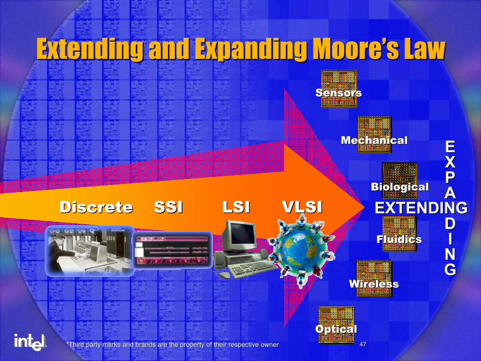
Extending and Expanding MooreExtending and Expanding Moore’’s Laws Law
SSISSISSI LSILSI VLSIVLSIDiscreteDiscrete
WirelessWireless
OpticalOptical
BiologicalBiological
SensorsSensors
FluidicsFluidics
MechanicalMechanical
EXTENDINGEXTENDING
EEXXPPAA
DDIINNGG
*Third party marks and brands are the property of their respecti*Third party marks and brands are the property of their respective ownerve owner 4848
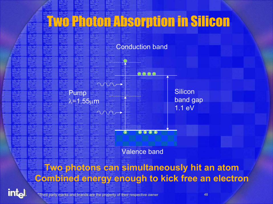
Two Photon Absorption in Silicon
Siliconband gap1.1 eV
Pumpλ=1.55µm
Valence band
Conduction band
Two photons can simultaneously hit an atomCombined energy enough to kick free an electron