® © 2003 intel corporation silicon photonics applications research results & integration...
Post on 21-Dec-2015
216 views
TRANSCRIPT

®
© 2003 Intel Corporation
Silicon Photonics Applications Research Results & Integration Challenges
Berkley Lecture Series: 4/27/04
Silicon Photonics Applications Research Results & Integration Challenges
Berkley Lecture Series: 4/27/04
Mario Paniccia, PhD.Mario Paniccia, PhD.
Director Photonics Technology LabDirector Photonics Technology Lab
Intel CorporationIntel Corporation
®
© 2003 Intel Corporation
Acknowledgements:Acknowledgements:
Drew Alduino, Sean Koehl, Richard Jones, Drew Alduino, Sean Koehl, Richard Jones, Ansheng Liu, Ling Liao, Mike Morse, Mike Salib, Ansheng Liu, Ling Liao, Mike Morse, Mike Salib, Dean Samara-RubioDean Samara-Rubio Oded Cohen, Doron Rubin, Assia BorkaiOded Cohen, Doron Rubin, Assia Borkai
• 3 •Communications TechnologyCommunications Technology
LabLab
© 2004 Intel Corporation
OutlineOutline
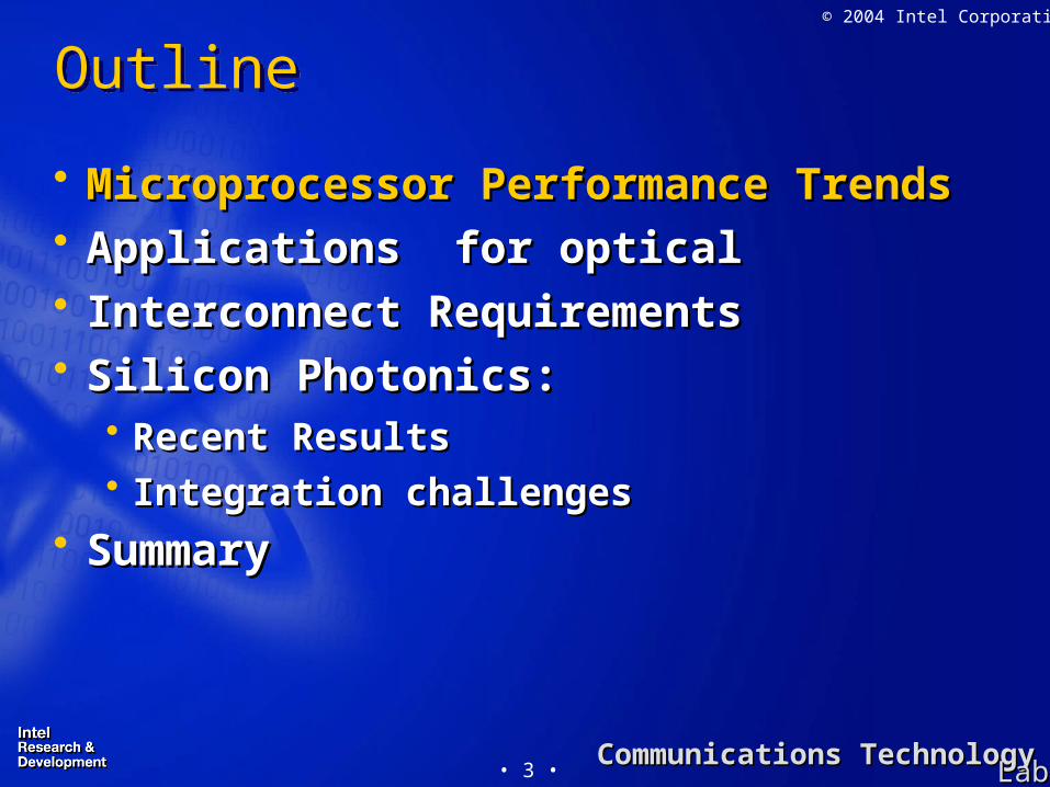
Microprocessor Performance TrendsMicroprocessor Performance Trends Applications for opticalApplications for optical Interconnect Requirements Interconnect Requirements Silicon Photonics: Silicon Photonics:
Recent ResultsRecent Results Integration challengesIntegration challenges
SummarySummary

• 4 •Communications TechnologyCommunications Technology
LabLab
© 2004 Intel Corporation
Moore’s Law Scaling: Moore’s Law Scaling:
4004400480808080
80868086
80088008
Pentium® ProcessorPentium® Processor
486™ DX Processor486™ DX Processor386™ Processor386™ Processor
286286
Pentium® II ProcessorPentium® II Processor
Pentium® III ProcessorPentium® III Processor Pentium® 4Pentium® 4ProcessorProcessor
Itanium® 2 ProcessorItanium® 2 Processor
1,0001,000
10,00010,000
100,000100,000
1,000,0001,000,000
10,000,00010,000,000
100,000,000100,000,000
1,000,000,0001,000,000,000
19701970 19801980 19901990 20002000 20102010
~ 1Billion transistors by end of decade~ 1Billion transistors by end of decade
Microprocessor transistor countMicroprocessor transistor count
Source: IntelSource: Intel

• 5 •Communications TechnologyCommunications Technology
LabLab
© 2004 Intel Corporation
Microprocessor PerformanceMicroprocessor Performance
Microprocessor clock frequency Microprocessor clock frequency trending to ~ 10GHz end of decadetrending to ~ 10GHz end of decade
Microprocessor clock frequency Microprocessor clock frequency trending to ~ 10GHz end of decadetrending to ~ 10GHz end of decade
Microprocessor Clock FrequencyMicroprocessor Clock Frequency
0.10.1
11
1010
100100
1,0001,000
10,00010,000
19701970 19801980 19901990 20002000 20102010
MHzMHz
Pentium® 4 ProcessorPentium® 4 Processor
Pentium® III ProcessorPentium® III ProcessorPentium® II ProcessorPentium® II Processor
Pentium® ProcessorPentium® Processor486™ Processor486™ Processor
386™ Processor386™ Processor286286
80868086
80858085
8080808040044004
Source: IntelSource: Intel

• 6 •Communications TechnologyCommunications Technology
LabLab
© 2004 Intel Corporation
PC or “Datacom” Economics:PC or “Datacom” Economics:
MIPSMIPS
PentiumPentium®®
ProcessorProcessor
PentiumPentium® ® ProProProcessorProcessor
PentiumPentium® ® IIIIProcessorProcessor
PentiumPentium® ® IIIIIIProcessorProcessor
PentiumPentium® ® 44ProcessorProcessor
Intel386Intel386TM TM DXDXMicroprocessorMicroprocessor
Intel486Intel486TMTM DX DX CPU CPU
MicroprocessorMicroprocessor
1
10
100
1000
10000
19851985 19891989 19931993 19951995 19971997 19991999 20012001
MIPS
$/MIPS$/MIPS
0.01
0.1
1
10
100
$/MIPS
1991199119871987
Higher Performance, Lower Cost

• 7 •Communications TechnologyCommunications Technology
LabLab
© 2004 Intel Corporation
OutlineOutline
Microprocessor Performance TrendsMicroprocessor Performance Trends Applications for opticalApplications for optical Interconnect Requirements Interconnect Requirements Silicon Photonics: Silicon Photonics:
Recent ResultsRecent Results Integration challengesIntegration challenges
SummarySummary
• 8 •Communications TechnologyCommunications Technology
LabLab
© 2004 Intel Corporation
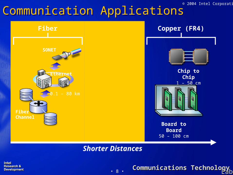
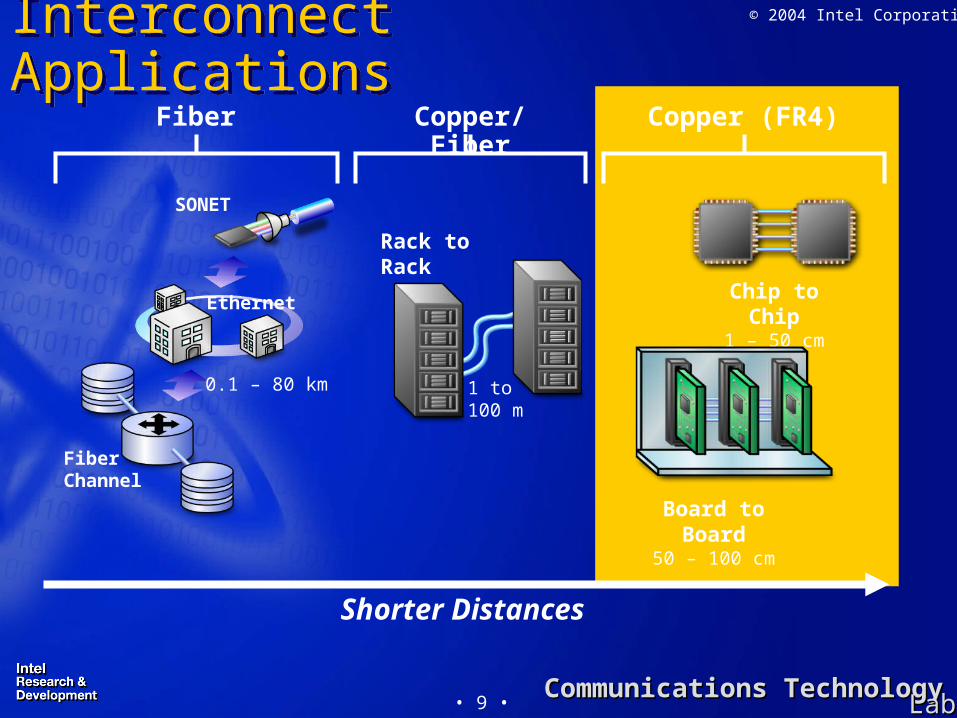
Chip to Chip1 – 50 cm
Board to Board50 – 100 cm
Copper (FR4)
Communication ApplicationsCommunication Applications
Shorter Distances
1 to 100 m
Rack to Rack
Copper/ FiberFiber
0.1 – 80 km
SONET
FiberChannel
Ethernet
• 9 •Communications TechnologyCommunications Technology
LabLab
© 2004 Intel Corporation
Chip to Chip1 – 50 cm
Board to Board50 – 100 cm
Copper (FR4)
Interconnect ApplicationsInterconnect Applications
Shorter Distances
1 to 100 m
Rack to Rack
Copper/ FiberFiber
0.1 – 80 km
SONET
FiberChannel
Ethernet

• 10 •Communications TechnologyCommunications Technology
LabLab
© 2004 Intel Corporation
OPTICALOPTICAL
Electrical to Optical: Bandwidth vs Cost Electrical to Optical: Bandwidth vs Cost
20042004 2010+2010+
ELECTRICALELECTRICAL
EnterpriseEnterpriseDistance: 0.1-Distance: 0.1-10km10km
Rack-RackRack-RackDistance: 1-100mDistance: 1-100m
Board-BoardBoard-BoardDistance: 50-Distance: 50-100cm100cm
Chip-ChipChip-ChipDistance: 1-50cmDistance: 1-50cm
3.125G 10G 3.125G 10G 40G 40G
3.125G 5-6G3.125G 5-6G 10G 10G 20G 20G
3.125G 5-6G3.125G 5-6G 10G 10G 15-20G 15-20G
Copper to optical transition is cost-driven
10G 10G >= 40G >= 40G
Cu TechnologyCu Technology(B/W)(B/W)
Optical CostsOptical Costs
Transition Zone
Transition Zone
Silicon Photonics?
• 11 •Communications TechnologyCommunications Technology
LabLab
© 2004 Intel Corporation
OutlineOutline
Microprocessor Performance TrendsMicroprocessor Performance Trends Applications for opticalApplications for optical Interconnect RequirementsInterconnect Requirements Silicon Photonics: Silicon Photonics:
Recent ResultsRecent Results Integration challengesIntegration challenges
SummarySummary
• 12 •Communications TechnologyCommunications Technology
LabLab
© 2004 Intel Corporation
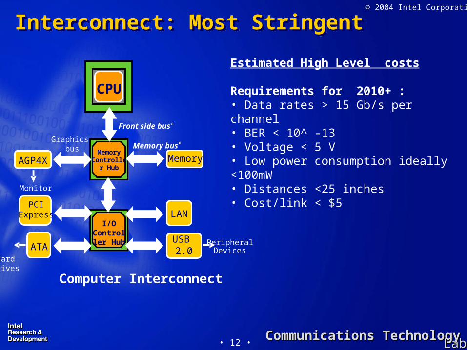
Interconnect: Most StringentInterconnect: Most Stringent
HardDrives
PCIExpress
ATA
CPU
Front side bus*
USB 2.0
PeripheralDevices
LAN
MCHMemory
Controller Hub
ICHI/O
Controller Hub
MemoryAGP4X
Monitor
Memory bus*Graphics
bus
Computer Interconnect
Estimated High Level costs
Requirements for 2010+ : • Data rates > 15 Gb/s per channel • BER < 10^ -13• Voltage < 5 V• Low power consumption ideally <100mW • Distances <25 inches• Cost/link < $5
• 13 •Communications TechnologyCommunications Technology
LabLab
© 2004 Intel Corporation
OutlineOutline
Microprocessor Performance TrendsMicroprocessor Performance Trends Applications for opticalApplications for optical Interconnect Requirements Interconnect Requirements Silicon Photonics: Silicon Photonics:
Opportunity & Recent ResultsOpportunity & Recent Results Integration challengesIntegration challenges
SummarySummary

• 14 •Communications TechnologyCommunications Technology
LabLab
© 2004 Intel Corporation
Opportunity for Silicon PhotonicsOpportunity for Silicon Photonics Take advantage of enormous (billions $$) of silicon
infrastructure and process learning Most tools exist: Lithography requirements do not
push leading edge (ie no 90nm litho) Integration opportunity to combine multiple optical
devices together (potential cost savings) Can use Silicon as workbench to assist with
packaging and alignment Opportunity to converge communication and
computing all on one platform..
Could provide PC like economics to Photonics Could provide PC like economics to Photonics However… many issues and challenges…However… many issues and challenges…
• 15 •Communications TechnologyCommunications Technology
LabLab
© 2004 Intel Corporation
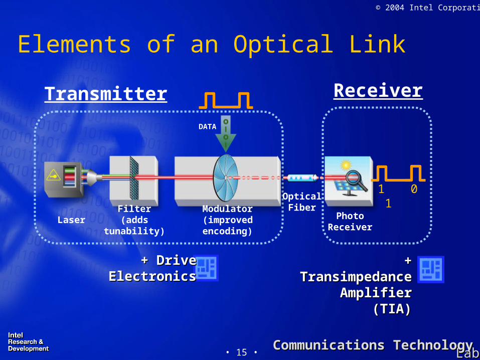
LaserFilter
(adds tunability)Photo
ReceiverModulator
(improved encoding)
DATA
OpticalFiber
1 0 1
Elements of an Optical Link
ReceiverTransmitter
+ + TransimpedanceTransimpedance
Amplifier (TIA)Amplifier (TIA)
+ Drive+ DriveElectronicsElectronics

• 16 •Communications TechnologyCommunications Technology
LabLab
© 2004 Intel Corporation
1. Light Source
2. Guide Light
3. Fast Modulation
4. Light Detection
5. Low-cost Assembly
6. Intelligence
Low-cost External Laser
Si on Insulator (SOI) WG
Si MOS Capacitor Device
Si Based Photodetector
Si Passive Alignment
Si CMOS Circuitry
REQUIREMENT OUR SOLUTION
Requirements for “Siliconizing” Photonics
Requirements for “Siliconizing” Photonics
• 17 •Communications TechnologyCommunications Technology
LabLab
© 2004 Intel Corporation
TIATIA
TIATIA
DriversDrivers
CMOSCMOSCircuitryCircuitry
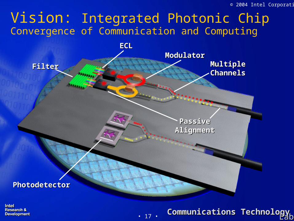
Vision: Integrated Photonic ChipConvergence of Communication and Computing
PhotodetectorPhotodetector
PassivePassiveAlignmentAlignment
ModulatorModulatorECLECL
FilterFilter MultipleMultipleChannelsChannels
• 18 •Communications TechnologyCommunications Technology
LabLab
© 2004 Intel Corporation
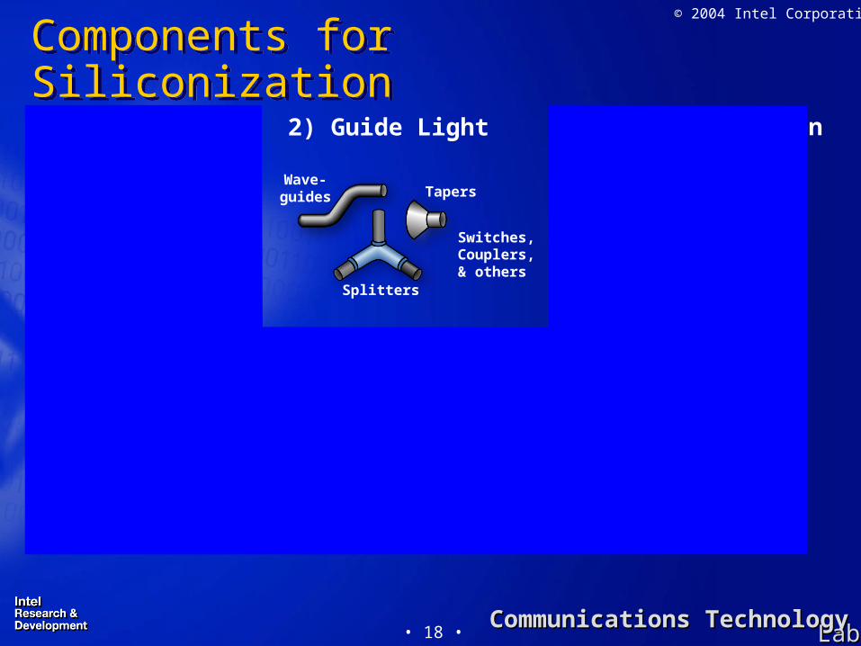
2) Guide Light
Wave-guides Tapers
Splitters
Switches,Couplers,& others
1) Light Source
External Cavity LaserLight Source
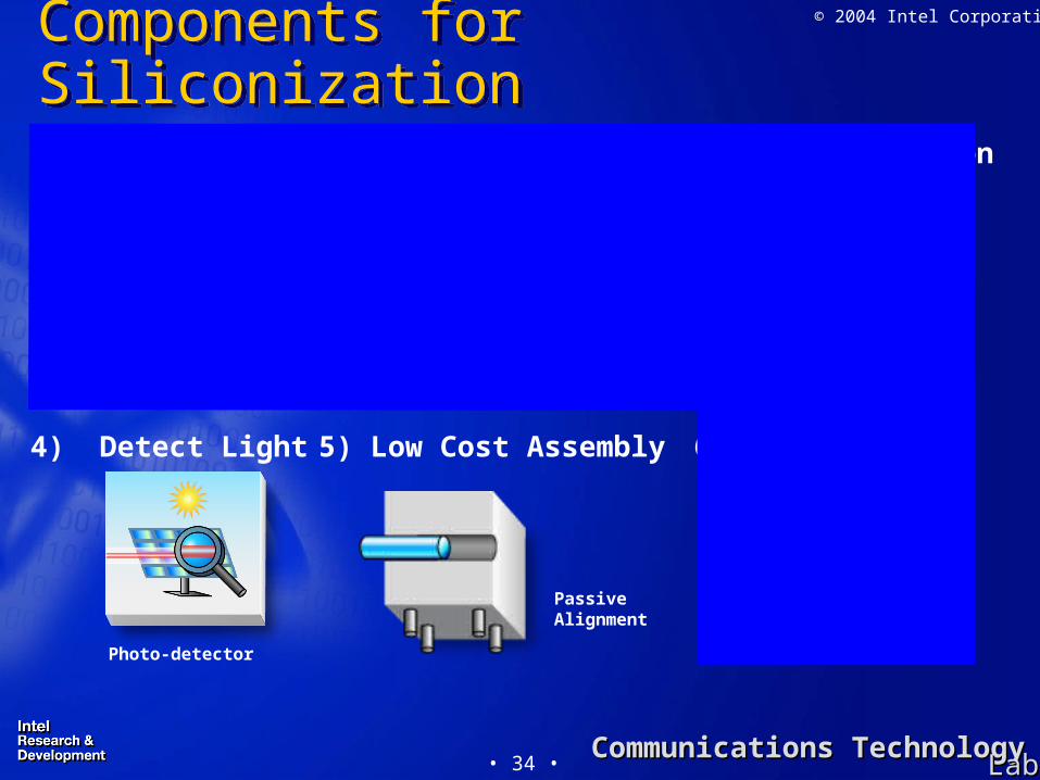
4) Detect Light
Photo-Detector
Components for SiliconizationComponents for Siliconization
6) Intelligence
CMOSCMOS
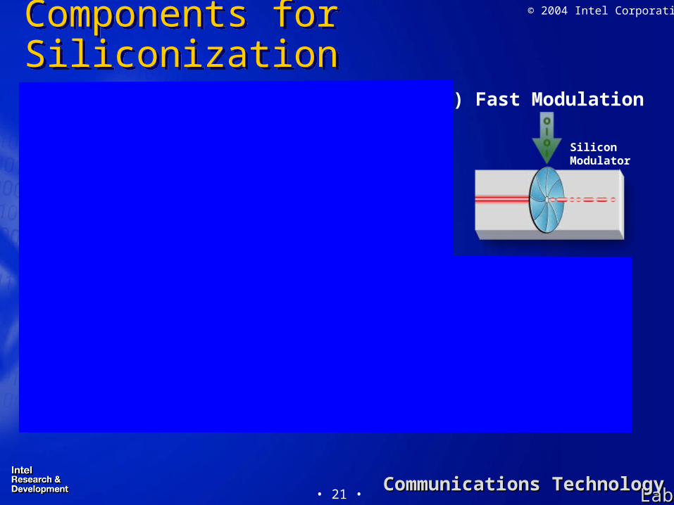
3) Fast Modulation
SiliconModulator
5) Low Cost Assembly
PassiveAlignment

• 19 •Communications TechnologyCommunications Technology
LabLab
© 2004 Intel Corporation
Photon Energy and Silicon Transparency
Photon Energy and Silicon Transparency
Ultra Violet (UV)
VisibleNear IR Far IR
Infra Red (IR)
E=hc/
Intel Litho
Photon Energy (eV) → 2.76 1.55 1.1eV 0.41Wavelength (µm) → 0.45 0.8 1.12µm 3.0
Silicon Opaque Silicon Transparent
Si Bandgap

• 20 •Communications TechnologyCommunications Technology
LabLab
© 2004 Intel Corporation
Guiding Light with Si WaveguidesGuiding Light with Si Waveguides
•Use silicon fabrication techniques to etch optical channels •The light is confined in the top Si layer between oxide layers•High index contrast (>2.5) allows for small bend radii
Rib waveguide
Silicon
oxide
SEM IMAGESSiliconoxide
• 21 •Communications TechnologyCommunications Technology
LabLab
© 2004 Intel Corporation
2) Guide Light
Wave-guides Tapers
Splitters
Switches,Couplers,& others
1) Light Source
External Cavity LaserLight Source
4) Detect Light
Photo-Detector
Components for SiliconizationComponents for Siliconization
6) Intelligence
CMOSCMOS
3) Fast Modulation
SiliconModulator
5) Low Cost Assembly
PassiveAlignment

• 22 •Communications TechnologyCommunications Technology
LabLab
© 2004 Intel Corporation
RESULTS: ModulatorRESULTS: Modulator Fast Modulators (>10GHz) exist, but use exotic
materials InP, Lithium Niobate etc
Fastest Si modulator to date was ~20MHz
Intel’s recent Research Breakthrough: Scalable 1GHz B/W silicon modulator
50 times faster than previous research attempts Published in the journal Nature on Feb-12, 2004
Uses novel “transistor-like” phase shifting device Simulations show this can scale to greater than 10GHz
Eliminates a significant barrier to making Photonic Devices in SiliconEliminates a significant barrier to making Photonic Devices in Silicon

• 23 •Communications TechnologyCommunications Technology
LabLab
© 2004 Intel Corporation
Modulator ConceptMach Zehnder Interferometer (MZI)Modulator ConceptMach Zehnder Interferometer (MZI)
Y coupler Y coupler/2
Silicon die
MZI Converts Phase shift into amplitude modulation
Optical Phase-Shifter
AmplitudeModulated
out
CW in
/2

• 24 •Communications TechnologyCommunications Technology
LabLab
© 2004 Intel Corporation
Novel Intel Capacitor Phase-shifterNovel Intel Capacitor Phase-shifter
Device x-section is transistor-like & operates in accumulation mode Uses Majority carriers, so speed is determined by RC only
•R controlled by doping, •C controlled by WG geometry and gate thickness
Trade off in size reduction, doping, and speed
oxide
Silicon
n-type Si
+
Gate Oxide p-type Polysilicon
OxideSilicon
Oxide
p-type Polysilicon

• 25 •Communications TechnologyCommunications Technology
LabLab
© 2004 Intel Corporation
Results: Phase vs Voltage (Active L: SOI h=1.4um, Poly .9um , Gox=120A)Results: Phase vs Voltage (Active L: SOI h=1.4um, Poly .9um , Gox=120A)
Moving to 60A Drive voltage can move to 3V
= 2nL/
indexncharge
N=0r/(etoxt)[VD-VFB]
Vfb~ 1.2V
Modeling
0 2 4 6 8 10
0.0
0.2
0.4
0.6
0.8
1.0 L=1.0 mm L=2.5 mm L=5.0 mm L=8.0 mm
Ph
ase
sh
ift
()
Drive voltage VD (V)
Vfb
Based on Plasma Optical Effect

• 26 •Communications TechnologyCommunications Technology
LabLab
© 2004 Intel Corporation
Results: MZI-modulatorResults: MZI-modulator L = 16.7L = 16.7m; 42nm FSR m; 42nm FSR (testing convenience)(testing convenience) Optical Loss:Optical Loss:
Passive WG 1.0 dB/cmPhase-shifter 5.1 dB/cm
Small-signal measurementsSmall-signal measurements Large-signal modulatorLarge-signal modulator
Phase shifters
Light
1cm
Light
2.5mm
Phase shifter
6.7 dB on-chip loss6.7 dB on-chip loss
• 27 •Communications TechnologyCommunications Technology
LabLab
© 2004 Intel Corporation
0.1 1-5
-4
-3
-2
-1
0
1
3 dB line
Opt
ical
res
pons
e (d
B)
Frequency (GHz)
0.1 110-4
10-3
10-2
On-chip voltage (V
)
Pho
to-r
ecei
ver o
utpu
t (V
)
Frequency (GHz)
10-2
10-1
100
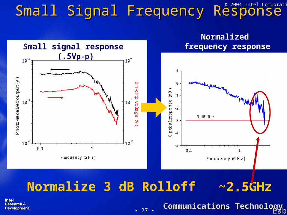
Small Signal Frequency ResponseSmall Signal Frequency Response
Normalize 3 dB Rolloff ~2.5GHz
Small signal response (.5Vp-p)
Normalized frequency response

• 28 •Communications TechnologyCommunications Technology
LabLab
© 2004 Intel Corporation
Large-signal ModulatorLarge-signal Modulator MZI has 1cm phase MZI has 1cm phase
shifter in each armshifter in each arm
Cap. load requires Cap. load requires parallel drive parallel drive
Bank of 8 differential Bank of 8 differential ECL buffersECL buffers
1.6V1.6Vpp pp
~5.8dB ER expected ~5.8dB ER expected
PRBS Source
CW in via lensed fiber. Polarization is controlled. MZI biased to quadrature by tuning . (FSR ~ 42nm)
3mm
+ -
Light output collected w/ lensed fiber DC-coupled 15GHz receiver

• 29 •Communications TechnologyCommunications Technology
LabLab
© 2004 Intel Corporation
Modulation Result: 1Gb/s Modulation Result: 1Gb/s Achieved 5dB RF extinction ratio Achieved 5dB RF extinction ratio Clearly recoverable 1Gb/s PRBS patternClearly recoverable 1Gb/s PRBS pattern
0.00
0.07
0.14
0.21
0.28
0.35
0 10 20 30 40 50Time (ns)
Pho
tore
ceiv
er O
utpu
t (V
)
70mV
225mV
PRBS Source Voltage (arb. units)
Extinction Ratio ~ 5dB

• 30 •Communications TechnologyCommunications Technology
LabLab
© 2004 Intel Corporation
2) Guide Light
Wave-guides Tapers
Splitters
Switches,Couplers,& others
1) Light Source
External Cavity LaserLight Source
4) Detect Light
Photo-detector
Components for SiliconizationComponents for Siliconization
6) Intelligence
CMOSCMOS
3) Fast Modulation
SiliconModulator
5) Low Cost Assembly
PassiveAlignment
• 31 •Communications TechnologyCommunications Technology
LabLab
© 2004 Intel Corporation
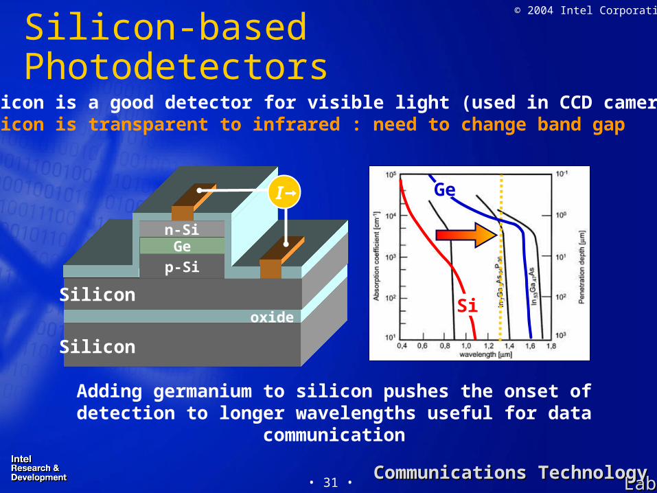
Silicon-based Photodetectors
Adding germanium to silicon pushes the onset of detection to longer wavelengths useful for data communication
Silicon is a good detector for visible light (used in CCD cameras)silicon is transparent to infrared : need to change band gap
Si
Ge
Silicon
Siliconoxide
Gen-Si
I
p-Si

• 32 •Communications TechnologyCommunications Technology
LabLab
© 2004 Intel Corporation
Previous Work on SiGe PhotodetectorsPrevious Work on SiGe PhotodetectorsReference Structure Efficiency Dark Current
Luyri et al. Ge p-i-n ex=40%@1.45 m 50 mA/cm2
Temkin et al. SiGe MQW pin int=40%@1.3 m 7 mA/cm2
Huang et al. SiGe MQW ex= 1%@1.3 m 60 mA/cm2
Huang et al. SiGeC ex= 1%@1.3 m 7 mA/cm2
Shuppert et al. SiGe MQW pin ex= 11%@1.3 m 1 mA/cm2
Samavedam et al. Ge pn diode ex= 13%@1.3 m 0.15 mA/cm2
Colace et al. Ge MSM ex= 23%@1.3 m 100 mA/cm2
Li et al. SiGe MQW pin ex= 1%@1.3 m no data
Oh et al. Ge pin ex= 49%@1.3 m 400 mA/cm2
Bauer et al. SiGe pin ex= 1%@1.3 m 40 mA/cm2
Goal SiGe pin waveguide ex=50% @1.3 m 1 mA/cm2
None of these have the desired performance and manufacturability to be commercially feasible.
• 33 •Communications TechnologyCommunications Technology
LabLab
© 2004 Intel Corporation
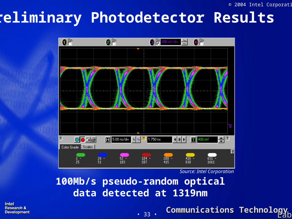
Preliminary Photodetector Results
100Mb/s pseudo-random optical data detected at 1319nm
Source: Intel Corporation
• 34 •Communications TechnologyCommunications Technology
LabLab
© 2004 Intel Corporation
2) Guide Light
Wave-guides Tapers
Splitters
Switches,Couplers,& others
1) Light Source
External Cavity LaserLight Source
4) Detect Light
Photo-detector
Components for SiliconizationComponents for Siliconization
6) Intelligence
CMOSCMOS
3) Fast Modulation
SiliconModulator
5) Low Cost Assembly
PassiveAlignment
• 35 •Communications TechnologyCommunications Technology
LabLab
© 2004 Intel Corporation
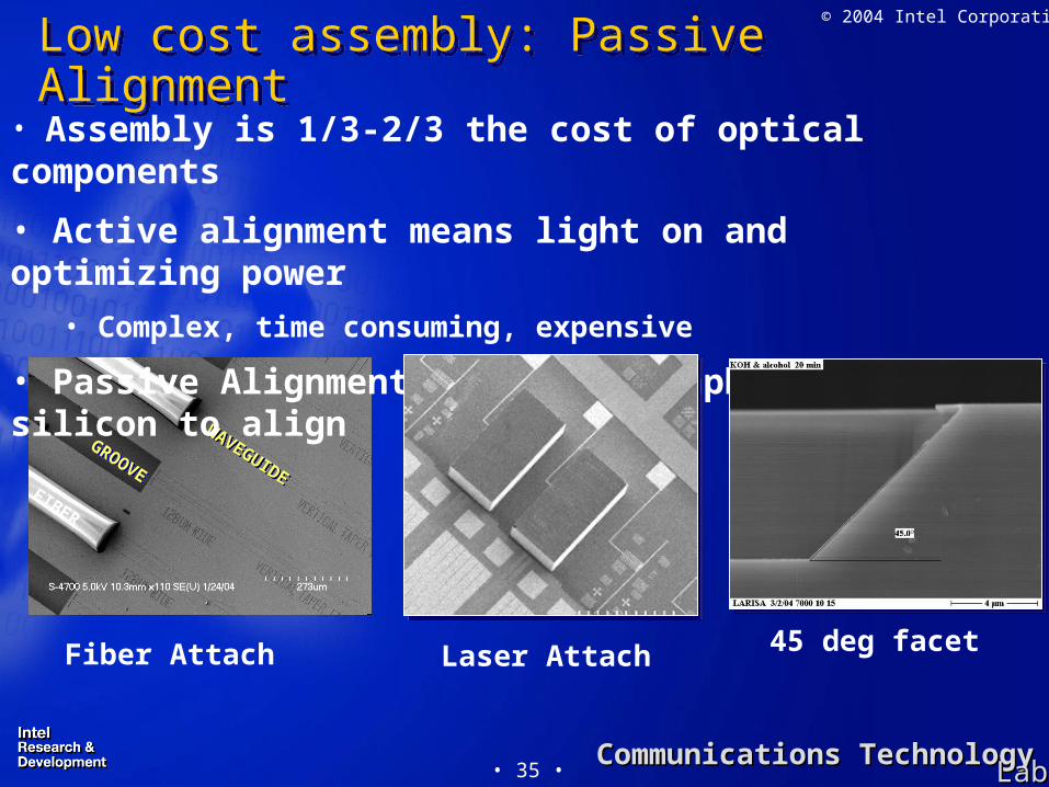
Low cost assembly: Passive AlignmentLow cost assembly: Passive Alignment
FIBER
WAVEGUIDE
WAVEGUIDE
GROOVE
GROOVE
• Assembly is 1/3-2/3 the cost of optical components
• Active alignment means light on and optimizing power
• Complex, time consuming, expensive
• Passive Alignment uses lithographically + silicon to align
Fiber Attach Laser Attach 45 deg facet

• 36 •Communications TechnologyCommunications Technology
LabLab
© 2004 Intel Corporation
Etched FacetEtched Facet •Develop a high quality waveguide facet etch (using a multi Develop a high quality waveguide facet etch (using a multi step etch recipe)step etch recipe)
• Deposit AR coating on Facet Deposit AR coating on Facet
..
Metallization IssuesMetallization Issues •Develop a metallization process with high bond strength Develop a metallization process with high bond strength
SOI Waveguide
Silicon Substrate
Challenges Challenges
Laser Diode
• 37 •Communications TechnologyCommunications Technology
LabLab
© 2004 Intel Corporation
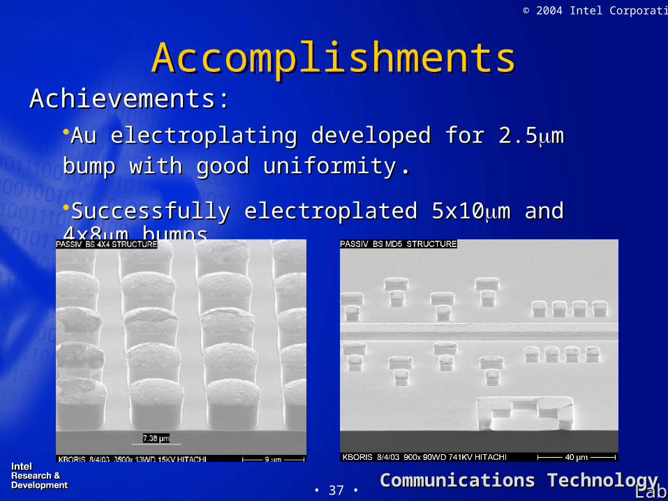
AccomplishmentsAccomplishmentsAchievements: Achievements:
Au electroplating developed for 2.5Au electroplating developed for 2.5m bump with good m bump with good
uniformityuniformity..
Successfully electroplated 5x10Successfully electroplated 5x10m and 4x8m and 4x8m bumpsm bumps

• 38 •Communications TechnologyCommunications Technology
LabLab
© 2004 Intel Corporation
First Bonding ResultsFirst Bonding Results
Mechanical die have been bonded to a patterned siliconwafer with 2.5m
thick electroplated Au bumps and
sheared off
0.5 mm
1 mm
0.25 mm

• 39 •Communications TechnologyCommunications Technology
LabLab
© 2004 Intel Corporation
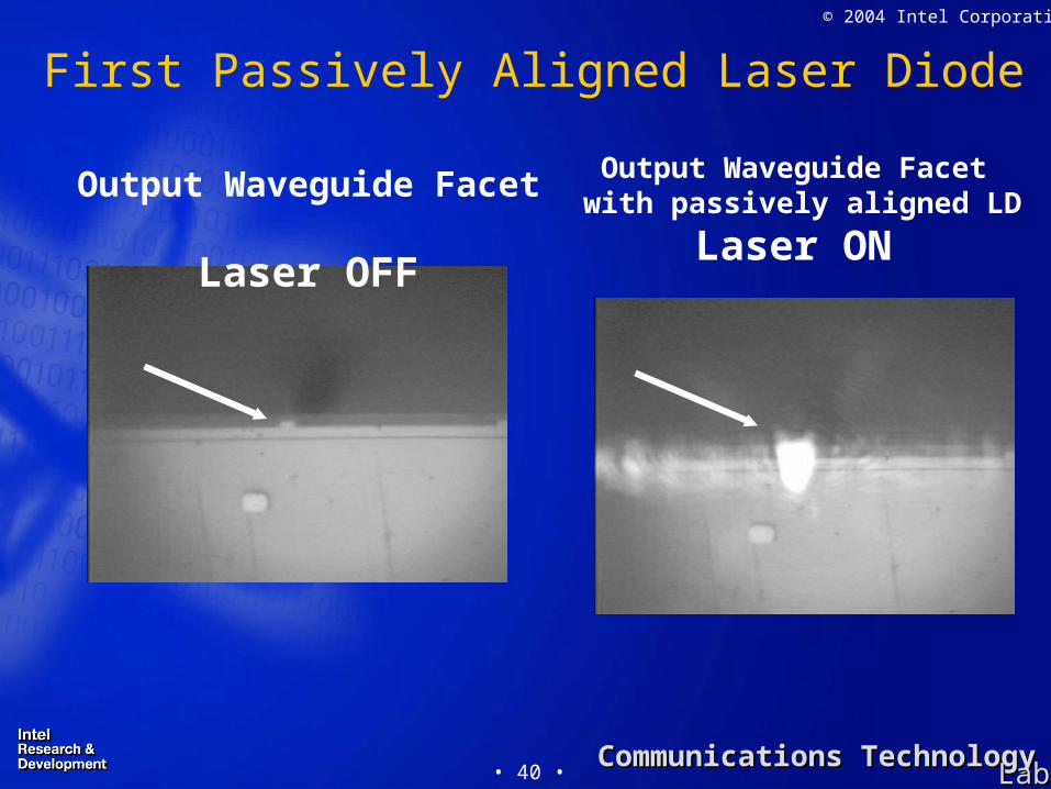
First Passively Aligned Laser DiodeFirst Passively Aligned Laser Diode
Top View
Output WaveguideFacet
Laser diode
ElectricalProbe
waveguide
• 40 •Communications TechnologyCommunications Technology
LabLab
© 2004 Intel Corporation
Output Waveguide Facet
Laser OFF
Output Waveguide Facet with passively aligned LD
Laser ON
First Passively Aligned Laser Diode

• 41 •Communications TechnologyCommunications Technology
LabLab
© 2004 Intel Corporation
Planar waveguide filtersPlanar waveguide filtersFiltersFilters Bragg filters ~ 2mm long x 2.5um wideBragg filters ~ 2mm long x 2.5um wide
Made from alternating polycrystalline Made from alternating polycrystalline silicon with crystalline silicon in waveguide silicon with crystalline silicon in waveguide ((n~0.01) narrow reflection bandn~0.01) narrow reflection band
70% reflectivity70% reflectivity 20dB extinction ratio20dB extinction ratio Stop band 0.5 - 5nmStop band 0.5 - 5nm Thermally tunable 12-nm/100-CThermally tunable 12-nm/100-C
ECLECL Used Bragg filters to wavelength stabilize Used Bragg filters to wavelength stabilize
external cavity laser external cavity laser Showed POC single mode ECLShowed POC single mode ECL Tunability same as gratingTunability same as grating Current researching SiON Bragg filters for Current researching SiON Bragg filters for
temperature stable devicetemperature stable device
Silicon / Poly silicon Bragg grating~ 0.5nm reflection band
Tuning of silicon based ECL with temperature
-25
-20
-15
-10
-5
0
1540 1545 1550 1555 1560
Wavelength (nm)
Op
tica
l po
wer
(d
B)
Silicon
Poly Silicon
-70
-60
-50
-40
-30
-20
-10
0
1538 1540 1542 1544 1546 1548
wavelength / nm
ou
tpu
t /
dB
m
25.6 C
29.5 C
34.8 C
39.9 C
47.1 C
52.6 C
59.6 C
66.6 C
71.1 C

• 42 •Communications TechnologyCommunications Technology
LabLab
© 2004 Intel Corporation
Coupling to Planar waveguide devicesCoupling to Planar waveguide devices
Coupling lossCoupling loss
Solution to large coupling Solution to large coupling loss is to taper from large loss is to taper from large input waveguide to smaller input waveguide to smaller bus waveguidebus waveguide
Showed Showed decreasedecrease in coupling in coupling loss to loss to 1.5dB/interface1.5dB/interface
Taper from 8umx8um to 2.5umx2.5um
THIS IS BIG CHALLENGE FOR SILICON PHOTONICS

• 43 •Communications TechnologyCommunications Technology
LabLab
© 2004 Intel Corporation
TIATIA
TIATIA
DriversDrivers
CMOSCMOSCircuitryCircuitry
Vision: Integrated Photonic ChipsConvergence of Communication and Computing
PhotodetectorPhotodetector
PassivePassiveAlignmentAlignment
ModulatorModulatorECLECL
FilterFilter MultipleMultipleChannelsChannels

• 44 •Communications TechnologyCommunications Technology
LabLab
© 2004 Intel Corporation
Integration Challenges w/CMOS FabricationIntegration Challenges w/CMOS Fabrication
Photonic IntegrationPhotonic Integration
Electronic (logic) & Photonic: Electronic (logic) & Photonic:
• 45 •Communications TechnologyCommunications Technology
LabLab
© 2004 Intel Corporation
Integrated solution must perform better or lower cost than sum of discrete components
Integration just for the sake of integration is not always good thing
Integration: Photonic Only Integration: Photonic Only
Monolithic integration of multiple optical devices has advantages:
1) Potential reduction in time and cost for testing vs hybrid 2) Litho alignment can reduce interface losses vs hybrid3) Packaging of one die vs multiple devices 4) New form factor/functionality that discrete devices may not provide
In the end though its all about balancing complexity vs yield

• 46 •Communications TechnologyCommunications Technology
LabLab
© 2004 Intel Corporation
Integration: Photonic & ElectronicIntegration: Photonic & Electronic
1) Process compatibility: • @ 10Gb/s CMOS IC’s need 90nm technology. • Silicon Photonic devices may only need ~.25um.
2) Yields: • Typical industry IC yields are very high, but the process windows are
extremely tight.• Combining photonics and CMOS could exceed thermal budget, DOF, and other processing guidelines, thereby reducing IC yield.
3) Potential for performance improvement at very high speeds
Size, form factor, power, performance & cost all factor into choosing Monolithic or Hybrid approach

• 47 •Communications TechnologyCommunications Technology
LabLab
© 2004 Intel Corporation
SummarySummary• Silicon Photonics could provide opportunity bring PC
economics to photonic industry
• Recent Results with silicon modulator have shown silicon to possibly be considered and optical material
• To be practical one must consider the integration challenges that will be encountered to produce these devices.
• In line wafer testing is big gap for HVM optical devices
• Electronic and photonic integration will be very challenging…

• 48 •Communications TechnologyCommunications Technology
LabLab
© 2004 Intel Corporation
Optical Modulator ReferencesOptical Modulator References
Ansheng Liu, Richard Jones, Ling Liao, Dean Samara-Rubio, Doron Rubin, Oded Ansheng Liu, Richard Jones, Ling Liao, Dean Samara-Rubio, Doron Rubin, Oded Cohen, Remus Nicolaescu, and Mario Paniccia, Cohen, Remus Nicolaescu, and Mario Paniccia, A high-speed silicon optical A high-speed silicon optical modulator based on a metal–oxide–semiconductor capacitormodulator based on a metal–oxide–semiconductor capacitor, , NatureNature 02/04 02/04
Tang, C. K. & Reed, G. T.Tang, C. K. & Reed, G. T., Highly efficient optical phase modulator in SOI , Highly efficient optical phase modulator in SOI waveguides. waveguides. Electron. Lett.Electron. Lett. 31, 451–452 (1995).31, 451–452 (1995).
Dainesi, P. Dainesi, P. et al.et al. CMOS compatible fully integrated Mach-Zehnder interferometer in CMOS compatible fully integrated Mach-Zehnder interferometer in SOI technology.SOI technology. IEEE Photon. Technol. Lett. IEEE Photon. Technol. Lett. 12, 660–662 (2000).12, 660–662 (2000).
Irace, A., Breglio, G. & Cutolo, A.Irace, A., Breglio, G. & Cutolo, A. All-silicon optoelectronic modulator with 1 GHz All-silicon optoelectronic modulator with 1 GHz switching capability. switching capability. Electron. Lett.Electron. Lett. 39, 232–233 (2003). 39, 232–233 (2003).
Hewitt, P.D.,Hewitt, P.D., Reed, G.T., Reed, G.T., Improving the response of optical phase modulators in Improving the response of optical phase modulators in SOI by computer simulation,SOI by computer simulation, J. Lightwave Technol. J. Lightwave Technol. 18, 443-450, (2000).18, 443-450, (2000).
Miller, D.A.B., Weiner, J.S., and Chemla, D.S.,Miller, D.A.B., Weiner, J.S., and Chemla, D.S., Electric field dependence of linear Electric field dependence of linear optical properties in quantum well structures: waveguide electroabsorption and optical properties in quantum well structures: waveguide electroabsorption and sum rules. sum rules. IEEE J. of Quantum Electron.IEEE J. of Quantum Electron. QE-22, 1816-1830 (1986) QE-22, 1816-1830 (1986)
Wooten, E. L. et al.Wooten, E. L. et al. A review of lithium niobate modulators for fiber-optic A review of lithium niobate modulators for fiber-optic communications systems. communications systems. IEEE J. Select. Topics Quant. Electron.IEEE J. Select. Topics Quant. Electron. 6, 69–82 (2000).6, 69–82 (2000).
• 49 •Communications TechnologyCommunications Technology
LabLab
© 2004 Intel Corporation
Silicon Photonics ReferencesSilicon Photonics References
Book: Silicon Photonics an Introduction by Graham T Reed , Book: Silicon Photonics an Introduction by Graham T Reed , Andrew Knights (Wiley) . March 2004Andrew Knights (Wiley) . March 2004
Silicon Photonics. Springer series topics in Applied Physics L. Silicon Photonics. Springer series topics in Applied Physics L. Pavesi, D. Lockwood (due out April 2004) Pavesi, D. Lockwood (due out April 2004)
For more info on Intel Research in Silicon Photonics , please visit: For more info on Intel Research in Silicon Photonics , please visit: www.intel.comwww.intel.com/technology/sp/technology/sp