signal integrity design of tsv-based 3d ic - · pdf filesignal integrity design of tsv-based...
TRANSCRIPT

Terahertz Interconnection and Package LaboratoryTERATerahertz Interconnection and Package Laboratory
1
Signal Integrity Design of TSV-Based 3D ICSignal Integrity Design of TSV-Based 3D IC
October 24, 2010Joungho Kim at KAIST
[email protected]://tera.kaist.ac.kr
Terahertz Interconnection and Package LaboratoryTERATerahertz Interconnection and Package Laboratory
2
Contents
1) Driving Forces of TSV based 3D IC
2) Signal Integrity Issues
3) Noise Coupling Issues
4) Noise Isolation Methods
5) Conclusion

Terahertz Interconnection and Package LaboratoryTERATerahertz Interconnection and Package Laboratory
3
TSV Based 3D ICTSV Based 3D IC
ADC, DACGPU ADC, DAC
RF
Analog
ADC, DAC Memory
Memory
Memory
Chip
Package
power
ground
PCB ground
p+ p+
n-welln+ n+
Inductor
NMOS Cap
Silicon Interposer

Terahertz Interconnection and Package LaboratoryTERATerahertz Interconnection and Package Laboratory
4
Major Advantages of TSV-based 3D IC
- Large interconnection density
- Small for factor
- High performance: high-bandwidth, high I/O counts
- Low power
- Potentially low cost

Terahertz Interconnection and Package LaboratoryTERATerahertz Interconnection and Package Laboratory
5
Multi-level On-chip Interconnect
Si-Substrate
SiO2
Under fill
Under fill
Dielectric
Dielectric
1st Chip
2nd Chip(Thinned
Substrate)
3rd Chip(Thinned
Substrate)
• Short Interconnection Length
� Reduced Delays� Low Impedance for PDN� Low Power Consumption
� Heat Dissipation Through Via
• Less Space for Interconnection� High Density Chip Wiring
� Large Number of I/O�Small Area Package
Key Technology for 3D IC: TSV (Through Silicon Via)Key Technology for 3D IC: TSV (Through Silicon Via)
3D TSV Stacked IC

Terahertz Interconnection and Package LaboratoryTERATerahertz Interconnection and Package Laboratory
6
High-frequency Channel Loss in TSVHigh-frequency Channel Loss in TSV
SiO2 Ta CuSi
S21
(mag
nitu
de)
[dB
]
Frequency [GHz]
0.1µµµµm

Terahertz Interconnection and Package LaboratoryTERATerahertz Interconnection and Package Laboratory
7
Frequency-dependent Loss of Through Silicon ViaFrequency-dependent Loss of Through Silicon Via
1-6
-5
-4
-3
-2
-1
0
Inse
rtio
n lo
ss (
dB)
Frequency (GHz)
10 200.1
Capacitiveregion
Resistiveregion
Cu SiO2 Si
Leakage current
Frequency dependent term
Loss term
Cinsulator GSi sub

Terahertz Interconnection and Package LaboratoryTERATerahertz Interconnection and Package Laboratory
8
Insulator thickness of TSV ↓
0.1 1 10-3.5
-3
-2.5
-2
-1.5
-1
-0.5
0
20
Frequency (GHz)
S21
mag
nitu
de (
dB)
( t = 0.5um )
( t = 0.3um )
( t = 0.1um )
[A]
TSV Channel Loss with Various Insulator Thickness of TSVTSV Channel Loss with Various Insulator Thickness of TSV
CInsulator /2 CInsulator /2
CInsulator /2 CInsulator /2
CInsulator =1.6 pF
CInsulator =2.6 pF
CInsulator =7.8 pF
Leakage current
Signal Top
Ground Top
SignalBottom
GroundBottom

Terahertz Interconnection and Package LaboratoryTERATerahertz Interconnection and Package Laboratory
9
Bump Bump
The Proposed TSV Equalizer using an Ohmic ContactThe Proposed TSV Equalizer using an Ohmic Contact
n-type Silicon
Substrate
n+ high doped Silicon
Ohmic contact(Al/n+ type)
SignalTSV
GroundTSV
Terahertz Interconnection and Package LaboratoryTERATerahertz Interconnection and Package Laboratory
10
0.1 1 10-8
-6
-4
-2
0
Inse
rtio
n lo
ss (
dB)
Frequency(GHz)20
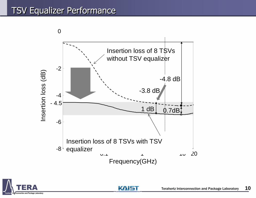
- 4.50.7dB1 dB
-3.8 dB
-4.8 dB
TSV Equalizer PerformanceTSV Equalizer Performance
Insertion loss of 8 TSVswithout TSV equalizer
Insertion loss of 8 TSVs with TSV equalizer

Terahertz Interconnection and Package LaboratoryTERATerahertz Interconnection and Package Laboratory
11
Eye opening by the TSV EqualizerEye opening by the TSV Equalizer
Time (ps)
0 10 08020 40 60
- 0 . 250 . 25
0
Vol
tage
(V
)
Time (ps)
0 10 08020 40 60
- 0 . 250 . 25
Pk-pk jitter : 16 ps
Eye opening: 10 0 mV
0
Vol
tage
(V
)

Terahertz Interconnection and Package LaboratoryTERATerahertz Interconnection and Package Laboratory
12
High speed channel loss by TSV
- High frequency loss
- Non uniform loss
- Loss increases as higher die stack and TSV numbers
- Passive and active equalization methods needed

Terahertz Interconnection and Package LaboratoryTERATerahertz Interconnection and Package Laboratory
13
Noise Coupling Paths in Stacked Dies using TSVNoise Coupling Paths in Stacked Dies using TSV
N-Well
N+ P+ P+ P+N+ N+
P-Substrate
P+N+ N+P+N+
N-Well
N+
N-Well
N-Well
N+ P+ P+ P+N+ N+
P-Substrate
P+N+ N+P+N+
N-Well
N+
N-Well
P-Substrate
1st Chip
2nd Chip
3rd Chip
TSV TSV
Inductor
Inductor
2
TSV to Active CircuitCoupling
3
Metal to MetalCoupling
1
TSV to TSVCoupling
TSV TSV
TSV TSV

Terahertz Interconnection and Package LaboratoryTERATerahertz Interconnection and Package Laboratory
14
Coupling between TSVsCoupling between TSVs
-14-
M
Gsi
Csi
R
L
Cox
Cm
Cp1
Freq [GHz]
-10
-20
-30
-40
-50
-60
0.1 1 10 20
Measurement
Model
Cox
Gsi
Csi
+ Cparasitics

Terahertz Interconnection and Package LaboratoryTERATerahertz Interconnection and Package Laboratory
15
Noise Coupling from TSV to Active CircuitsNoise Coupling from TSV to Active Circuits
Cou
plin
g co
effic
ient
[dB
]
silicon substrate
contact
TSV
ILD/IMD
Distance between contact and TSV : 100 μμμμmSubstrate height : 100 μμμμmTSV diameter : 30 μμμμmTSV SiO2 thickness : 0.5 μμμμm
CTSV
Rsub
Csub
A B C
10M 100M 1G 10G-60
-55
-50
-45
-40
-35
-30
TSV SiO2 capacitance dominant
Silicon resistance dominant
Silicon capacitance
dominant
Frequency [GHz]

Terahertz Interconnection and Package LaboratoryTERATerahertz Interconnection and Package Laboratory
16
Shielding Methods for TSV Coupling

Terahertz Interconnection and Package LaboratoryTERATerahertz Interconnection and Package Laboratory
17-17-
Shielding Effect Measurement: Guard RingShielding Effect Measurement: Guard Ring
-10
-20
-30
-40
-50
-600.1 1 10 20
Freq [GHz]
w/o guard ring
w/ guard ring

Terahertz Interconnection and Package LaboratoryTERATerahertz Interconnection and Package Laboratory
18
Shielding Methods for TSV Coupling

Terahertz Interconnection and Package LaboratoryTERATerahertz Interconnection and Package Laboratory
19
Crosstalk between TSV
- High frequency coupling
- Dependent on TVS designs: dimensions and materials
- Proper shielding methods are needed
- Shielding structures can be significant overhead of chip area
- Special I/O scheme may be needed to compensate or to avoid the
crosstalk effects
Terahertz Interconnection and Package LaboratoryTERATerahertz Interconnection and Package Laboratory
20
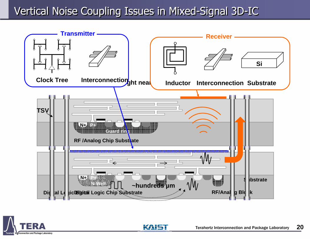
Only tens µm distance : Tight near-field coupling a nd conductive coupling
N-WellN+ P+
Vertical Noise Coupling Issues in Mixed-Signal 3D-ICVertical Noise Coupling Issues in Mixed-Signal 3D-IC
Noise coupling through silicon substrate in 2D SoC
Digital Logic Block RF/Analog Block
Substrate~hundreds µm
InterconnectionInductor Substrate
Si
Receiver
~tens µm
Digital Logic Chip Substrate
N+ P+
RF /Analog Chip Substrate
TSV
Guard ring
Clock Tree Interconnection
Transmitter

Terahertz Interconnection and Package LaboratoryTERATerahertz Interconnection and Package Laboratory
21
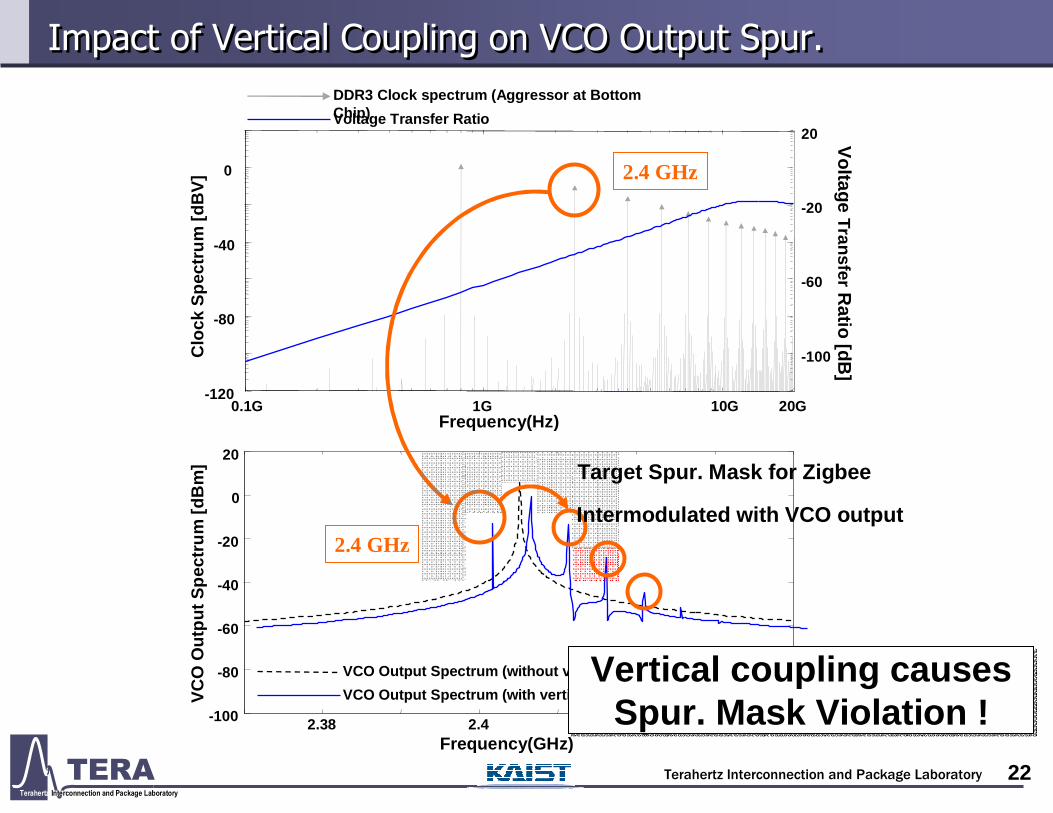
3D IC for 2.4GHz VCO in Zigbee module3D IC for 2.4GHz VCO in Zigbee module
Vertical Coupling Path Model
Port #2 Port #3
Differential On-Chip Inductor Model
On-Chip Clock Tree Model
Port #1
Vcontrol Vout ++
-
Vbias
Vout -
VD
D
L(1nH) L (1nH)
Port #2 Port #3
Spur. & Phase noise at VCO output
Clock Tree
VDD
3 turnDifferential On-Chip Inductor
Noise Source at Port #1 : DDR 3 Clock
Rising/Falling Time (Tr/Tf) 35ps
Operation Frequency(1/TD)800MHz (1.25ns)
V peak 1.5V
Terahertz Interconnection and Package LaboratoryTERATerahertz Interconnection and Package Laboratory
22
Impact of Vertical Coupling on VCO Output Spur. Impact of Vertical Coupling on VCO Output Spur.
VC
O O
utpu
t Spe
ctru
m [d
Bm
]
Frequency(GHz)2.38 2.4 2.42 2.44-100
-80
-60
-40
-20
0
20
Clo
ck S
pect
rum
[dB
V]
Voltage Transfer
Ratio [dB
]
Frequency(Hz)
-120
-100
-80
-60
-40
-20
0
20
0.1G 1G 10G 20G
2.4 GHz
2.4 GHz
Voltage Transfer Ratio
DDR3 Clock spectrum (Aggressor at Bottom Chip)
VCO Output Spectrum (with vertical coupling)
VCO Output Spectrum (without vertical coupling)
Target Spur. Mask for Zigbee
Intermodulated with VCO output
Vertical coupling causesSpur. Mask Violation !
Vertical coupling causesSpur. Mask Violation !
Terahertz Interconnection and Package LaboratoryTERATerahertz Interconnection and Package Laboratory
23
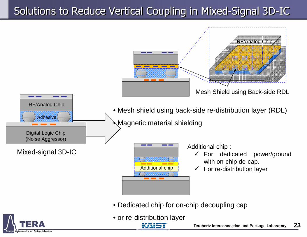
Solutions to Reduce Vertical Coupling in Mixed-Signal 3D-ICSolutions to Reduce Vertical Coupling in Mixed-Signal 3D-IC
RF/Analog Chip
Adhesive
Digital Logic Chip (Noise Aggressor)
Additional chip
Additional chip : � For dedicated power/ground
with on-chip de-cap.� For re-distribution layer
• Dedicated chip for on-chip decoupling cap
• or re-distribution layer
Mixed-signal 3D-IC
RF/Analog Chip
RF/Analog Chip
Mesh Shield using Back-side RDL
• Mesh shield using back-side re-distribution layer (RDL)
• Magnetic material shielding
Terahertz Interconnection and Package LaboratoryTERATerahertz Interconnection and Package Laboratory
24
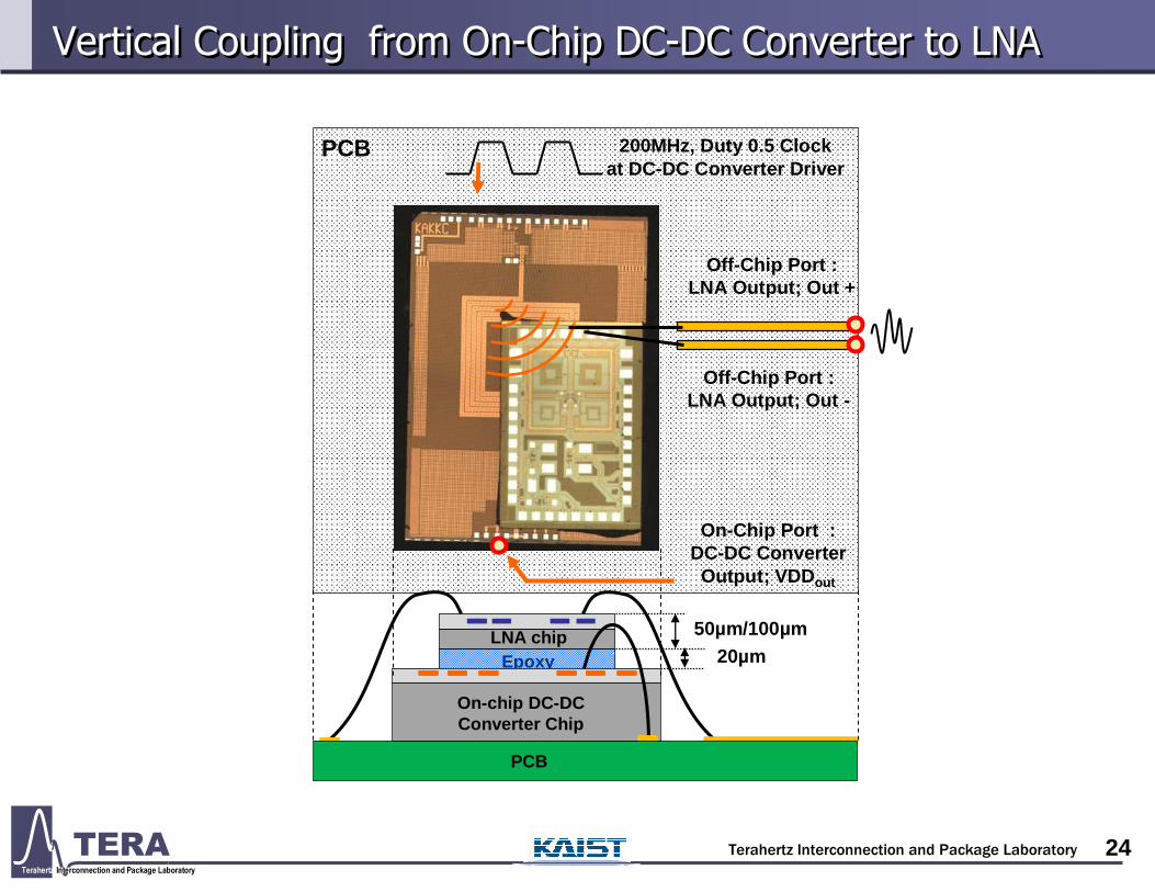
Vertical Coupling from On-Chip DC-DC Converter to LNAVertical Coupling from On-Chip DC-DC Converter to LNA
LNA chip 50µm/100µm20µmEpoxy
PCB
On-chip DC-DC Converter Chip
PCB
200MHz, Duty 0.5 Clock at DC-DC Converter Driver
Off-Chip Port :LNA Output; Out +
Off-Chip Port :LNA Output; Out -
On-Chip Port : DC-DC Converter Output; VDD out
PCB

Terahertz Interconnection and Package LaboratoryTERATerahertz Interconnection and Package Laboratory
25
Inductive and Capacitive Coupling ModelInductive and Capacitive Coupling Model
VDD
On-chip
Out+
50ΩΩΩΩ
12nH
Equiv. Model of Q2
37nHQ1
Q2
VDDin
VDDout
On-chip
Simplified Model of On-Chip DC-DC Converter
Simplified Model of LNA
LM = 600pHCC = 60fF

Terahertz Interconnection and Package LaboratoryTERATerahertz Interconnection and Package Laboratory
26
• Vertical coupling from DC-DC Converter to LNA
� ~40mVpp ripple at VDD out ���� 88mVpp /48mVpp coupled noise at LNA Out +/-
� Typical RF signal at LNA output: start from -90dBm (20µVpp with 50 ΩΩΩΩ load)
Measurement of Vertical Coupling :
Measurement of Vertical Coupling :
LNAOut-
LNAOut+
On-Chip Port : DC-DC Converter Outut;
VDDout
?
0 0.2 0.4 0.6 0.8 1 1.2 1.4 1.6 1.8 2
x 10-8
-0.04
-0.03
-0.02
-0.01
0
0.01
0.02
0.03
0.04
0.05
0.06
-40
-20
0
20
40
60
Cou
pled
Noi
se a
t LN
A o
utpu
t(m
V)
0 2 4 6 8 10 12 14 16 18 20
Time from Triggered point(ns)
LNA Out+
LNA Out-DUT 1-50µm
5ns (200MHz)
Terahertz Interconnection and Package LaboratoryTERATerahertz Interconnection and Package Laboratory
27
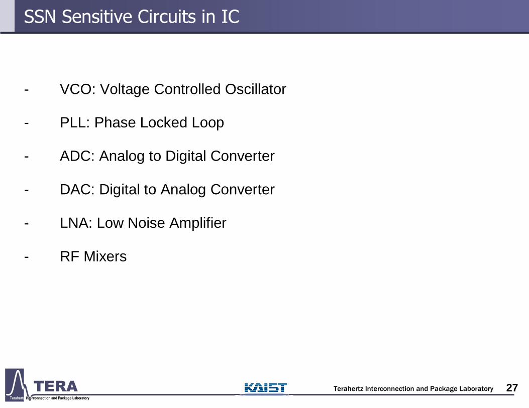
SSN Sensitive Circuits in IC
- VCO: Voltage Controlled Oscillator
- PLL: Phase Locked Loop
- ADC: Analog to Digital Converter
- DAC: Digital to Analog Converter
- LNA: Low Noise Amplifier
- RF Mixers

Terahertz Interconnection and Package LaboratoryTERATerahertz Interconnection and Package Laboratory
28
Hierarchical PDN in 3D ICHierarchical PDN in 3D IC
ADC, DACGPU ADC, DAC
RF
Analog
ADC, DAC Memory
Memory
Memory
Chip
Package
power
ground
PCB ground
p+ p+
n-welln+ n+
Inductor
NMOS Cap
Silicon Interposer

Terahertz Interconnection and Package LaboratoryTERATerahertz Interconnection and Package Laboratory
29
PDN Impedance Curves in 3D ICPDN Impedance Curves in 3D ICFigure Figure Figure Figure Peak Peak Peak Peak
( region V )( region V )( region V )( region V )Mode numberMode numberMode numberMode number
Fig. 3-(a)
a, b, d, f (1,0), (2,0), (3,0), (4,0)/(0,1)
- Mode @ DRAM
c, e (2,1), (3,1)- Mode @ Interposer

Terahertz Interconnection and Package LaboratoryTERATerahertz Interconnection and Package Laboratory
30
30
PDN Impedance of 3D IC with On-chip Decoupling CapacitorsPDN Impedance of 3D IC with On-chip Decoupling Capacitors

Terahertz Interconnection and Package LaboratoryTERATerahertz Interconnection and Package Laboratory
31
Lowering PDN impedance in TSV based 3D IC
- On-chip and Off-chip decoupling capacitors
- Lower inductance TSV,
- Higher number of TSV
- Lower inductance of PDN interconnections in RDL, on-chip, and
interposer
- Lower resistance of PDN interconnections in RDL, on-chip, and
interposer

Terahertz Interconnection and Package LaboratoryTERATerahertz Interconnection and Package Laboratory
32
PDN Noise coupling pathes in3D ICPDN Noise coupling pathes in3D IC
ADC, DACGPU ADC, DAC
RF
Analog
ADC, DAC Memory
Memory
Memory
Chip
p+ p+
n-welln+ n+
Inductor
NMOS Cap
Silicon Interposer
Package
power
ground
PCB ground

Terahertz Interconnection and Package LaboratoryTERATerahertz Interconnection and Package Laboratory
33
SSN Noise Coupling Paths
- On-chip and Off-chip PDN
- Si substrate
- Interposer substrate
- RDL patterns
- TSV
- Coupling

Terahertz Interconnection and Package LaboratoryTERATerahertz Interconnection and Package Laboratory
34
Clock Jitter Due to the SSN CouplingClock Jitter Due to the SSN Coupling
� w/o PDN Noise �100MHz PDN Noise
1.45 ps 321.4 ps
Noise Level
�800MHz PDN Noise
33 ps
�1GHz PDN Noise
2.3 ps
Duty Cycle Distortion

Terahertz Interconnection and Package LaboratoryTERATerahertz Interconnection and Package Laboratory
35
Jitter w/o and w PDN ModelsJitter w/o and w PDN Models
10 100M 1G0
50
100
150
200
250
300
350
10-3
10-2
10-1
100
101
Cou
plin
g R
atio
Jitte
r (p
s)
Noise Freq. (Hz)
Noise level : 100 mV Voltage of SSN w/o PDN models
Jitter due to SSN w/o PDN models
Voltage of SSN w PDN models
Jitter due to SSN w PDN modelsInput Clock Frequency of DLL = 1 GHz
Terahertz Interconnection and Package LaboratoryTERATerahertz Interconnection and Package Laboratory
36
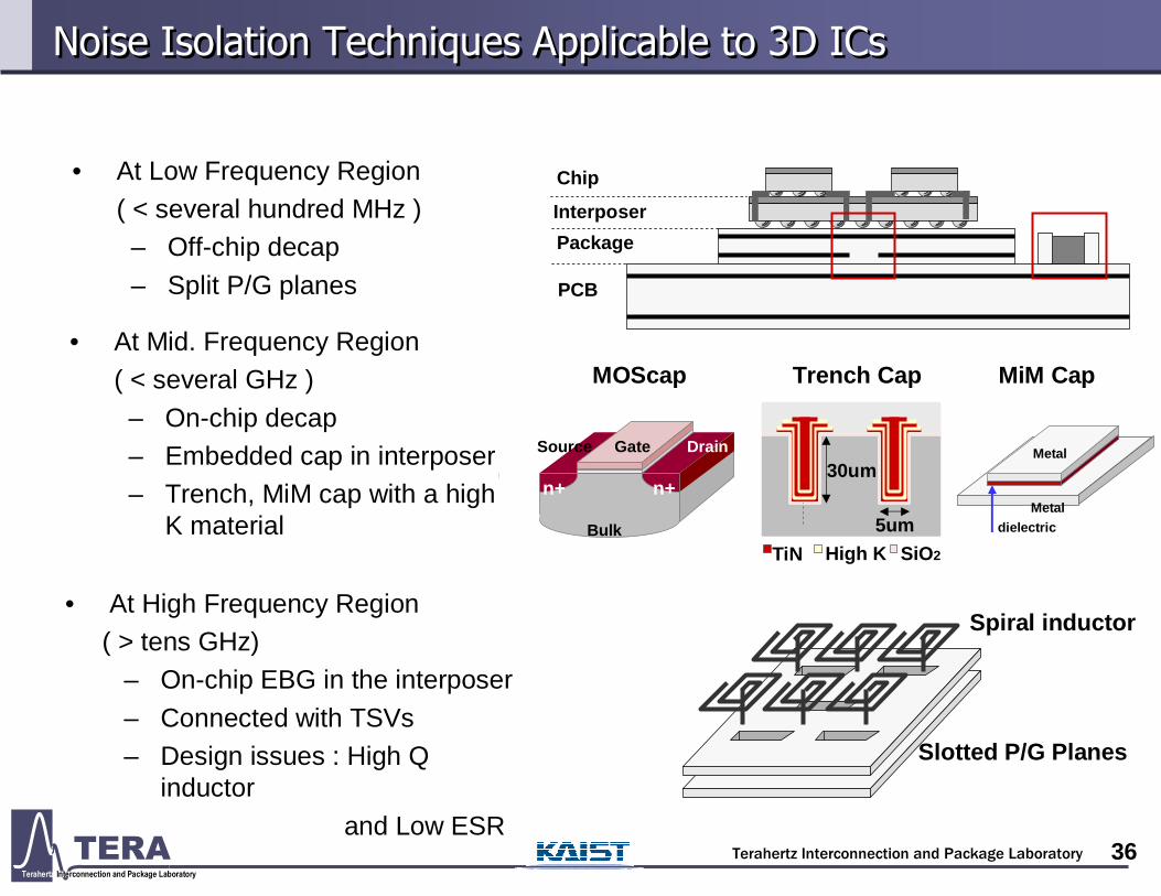
PCB
Package
Interposer
Chip
Noise Isolation Techniques Applicable to 3D ICsNoise Isolation Techniques Applicable to 3D ICs
• At Low Frequency Region ( < several hundred MHz )– Off-chip decap
– Split P/G planes
• At Mid. Frequency Region( < several GHz )
– On-chip decap– Embedded cap in interposer– Trench, MiM cap with a high
K material
• At High Frequency Region( > tens GHz)
– On-chip EBG in the interposer
– Connected with TSVs– Design issues : High Q
inductor
and Low ESR
n+ n+
GateSource Drain
Bulk
TiN High K SiO2
5um
30umMetal
Metaldielectric
MOScap Trench Cap MiM Cap
Spiral inductor
Slotted P/G Planes

Terahertz Interconnection and Package LaboratoryTERATerahertz Interconnection and Package Laboratory
37
On-Interposer EBG StructureOn-Interposer EBG Structure
Capacitive P/G mesh
Inductive P/G mesh
Width: 80um
Space: 120um
Width: 40um
Space: 360um
WS
W
S

Terahertz Interconnection and Package LaboratoryTERATerahertz Interconnection and Package Laboratory
38
Measurement Results of On-interposer EBG Measurement Results of On-interposer EBG
0 2 4 6 8 10 12 14 16 18 20-90
-80
-70
-60
-50
-40
-30
-20
-10
0
Frequency (GHz)
Co
uplin
g C
oe
ffic
ient
s, S
21
(dB
)
TV A (Mesh)TV B (EBG)
Stopband
Mesh PDN
Interposer EBG

Terahertz Interconnection and Package LaboratoryTERATerahertz Interconnection and Package Laboratory
39
Measurement Results of On-interposer EBG Measurement Results of On-interposer EBG
0 2 4 6 8 10 12 14 16 18 20-70
-60
-50
-40
-30
-20
-10
Frequency (GHz)
Coup
led
Nois
e S
pect
rum
(dB
m)
TV A (Mesh)TV B (EBG)
1GHz

Terahertz Interconnection and Package LaboratoryTERATerahertz Interconnection and Package Laboratory
40
On-chip CMOS Active EBGOn-chip CMOS Active EBG
1.2 mm
1.5
mm
W inductor
W inductor
t top
Spiral inductor
Port 1 Port 2
Si-substrate NMOS cap.

Terahertz Interconnection and Package LaboratoryTERATerahertz Interconnection and Package Laboratory
41
SEM Photograph of On-chip Active CMOS EBG SEM Photograph of On-chip Active CMOS EBG
M6
M5M4M3M2M1
tmetal
Viat IMD
t top
Gate (1µm) Gate finger
Spiral inductor (portion)
Si-substrate
* MagnaChip 0.18 μμμμm standard CMOS Process
Terahertz Interconnection and Package LaboratoryTERATerahertz Interconnection and Package Laboratory
42
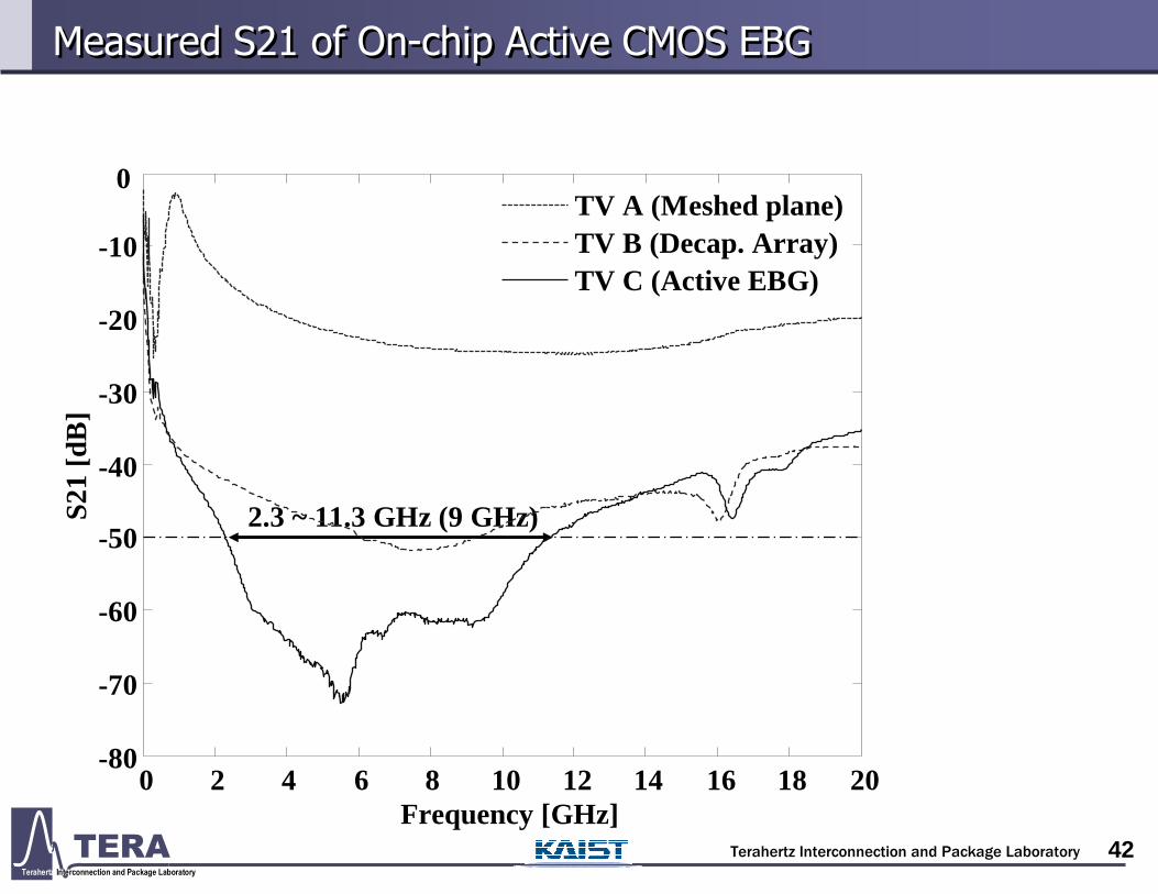
Measured S21 of On-chip Active CMOS EBG Measured S21 of On-chip Active CMOS EBG
2.3 ~ 11.3 GHz (9 GHz)
0 2 4 6 8 10 12 14 16 18 20-80
-70
-60
-50
-40
-30
-20
-10
0
Frequency [GHz]
S21
[dB
]
TV A (Meshed plane)TV B (Decap. Array)TV C (Active EBG)

Terahertz Interconnection and Package LaboratoryTERATerahertz Interconnection and Package Laboratory
43
Tuning of On-chip Active CMOS EBG Tuning of On-chip Active CMOS EBG
0 2 4 6 8 10 12 14 16 18 20-80
-70
-60
-50
-40
-30
-20
-10
0
Frequency [GHz]
S21
[dB
]
2.3 ~ 11.3 GHz
4.7 ~ 13.3 GHz
TV C with 0V power (OFF)TV C with 1.8V power (ON)

Terahertz Interconnection and Package LaboratoryTERATerahertz Interconnection and Package Laboratory
44
Measured SSN Waveforms with a 3-GHz Clock Noise InputMeasured SSN Waveforms with a 3-GHz Clock Noise Input
0 0.5 1 1.5-150
-100
-50
0
50
100
150
Time [ns]
Cou
pled
SS
N [
mV
]
0 0.5 1 1.5-150
-100
-50
0
50
100
150
Time [ns]
Cou
pled
SS
N [
mV
]
0 0.5 1 1.5-150
-100
-50
0
50
100
150
Time [ns]
Cou
pled
SS
N [
mV
]
0 0.5 1 1.5-150
-100
-50
0
50
100
150
Time [ns]
Cou
pled
SS
N [
mV
]
259.7mV
16.5mV
5.1mV23.4mV
(a) (b)
(c) (d)
TV A TV B
TV C with 0V power TV C with 1.8V power

Terahertz Interconnection and Package LaboratoryTERATerahertz Interconnection and Package Laboratory
45
Summary
-TSV is the most critical interconnection structure in 3D IC.
- TSV can cause significant channel loss for high-speed signaling.
- Equalizer or specific I/O schemes are needed to support low power
and high-speed data transmissions.
-Crosstalk and coupling between TSV and active circuit need to be
considered when designing the TSV arrangement configurations.
-Vertical coupling should be considered in mixed mode 3D IC.
- Shielding structures are needed to reduce the TSV crosstalks and noise
couplings.