signal integrity basics · 2016-03-18 · 1 signal integrity basics by anritsu field application...
TRANSCRIPT

1
Signal Integrity Basics
By Anritsu Field Application Engineers
TABLE OF CONTENTS
1.0 Bits, Bytes and Hertz 2.0 Eye Patterns 3.0 Pulse Composition 4.0 Common Causes of Pulse Distortion 5.0 Measurements
Introduction Digital Signal Integrity (SI) can be described simply as the study of pulse distortion. Historically, pulsed signals were measured with an oscilloscope or digital signal analyzer. With the advent of today’s Gigabit data rates, Bit Error Rate Testing (BERT) has become the measurement of choice. Since PC‘s are targeted to reach eight Gigabits per second (Gbps) in the near future, the digital community has been forced to solve the types of analog problems that RF/MW engineers live with on a daily basis. Therefore, measurements such as SWR, insertion loss, leakage between printed tracks and delay times, have become parameters that now must be evaluated by digital designers to assure “pulse fidelity.” Testing is further complicated by the fact that balanced lines and circuits are used to reduce interference. And, when many complex circuits are compressed onto a multilayer PC board, the difficulty increases. On top of that, it is a challenge to contact the desired point on the circuit, since it may be accessed only by using destructive procedures. Test connectors located at strategic points in the circuit offer one solution; however, they not only occupy valuable real estate, they may introduce their own set of problems. Bits, Bytes and Hertz The Frequency (Hz) is the speed of the pattern at 1 cycle / second in the frequency domain, while the bits are a logical 1 or 0 in the pattern itself, measured as 1 bit / second within the time domain. Without any modulation or compression, 1 Hz = 1 bit, so 100hz is equal to 100 bits/. However, this is not always the case. For example, 100BASE-TX has a specified data rate of 100 Mbits / second and operates at 33 MHz. This is because 100BASE-TX uses compression. Hertz and bits can be interchangeable and it is possible to go back and forth mathematically between the frequency and time domains with the Fast Fourier transform. Test tools, such as network analyzers, perform these calculations.

2
Of course, in this high-speed world, these basic units become Gigabits, Gigabytes, and Gigahertz. A path capable of passing 8 GHz with minimal roll-off will be able to pass a clock rate of 16 Gbps. This equates to two Gigabytes per second, since a nominal byte has eight bits. Figures 1, 2 and 3 illustrate how logic circuits must distinguish “1”s from “0”s:
. Figure 1.
Good pulse pattern.
Figure 2.
Acceptable pulse pattern.

3
Figure 3.
Poor pulse pattern. Eye Patterns An eye diagram is the result of superimposing the 1’s, 0’s and corresponding transitions of a high- speed digital signal onto a single amplitude, versus time display. As shown in Figure 4, the resulting waveform resembles an eye, hence the name eye diagram. The time axis can be normalized for 2 bits (as shown) for easy viewing, with the 1-bit “eye opening” in the center of the display and one-half bit on both left and right of the center eye (for viewing transitions).
� Transitions in the digital signal that infringe on the center of the eye can eventually cause errors.
� In general, the more open the eye, the lower the likelihood that the receiver in a transmission system may mistake a logical 1 bit for a logical 0 bit, or vice versa. The percentage of bits that have errors compared to the overall bits is called Bit Error Ratio (BER); the lower the BER the better.
� It’s important to note that the eye diagram does not show protocol or logic problems. Using this eye diagram, we can easily view signal impairments in the physical layer – in terms of amplitude and time distortion.

4
Figure 4.
Ideal eye pattern.
Figure 5.
Acceptable eye pattern.

5
Figure 6.
Poor eye pattern. Pulse Composition (X axis is time) An ideal rectangular waveform is formed by adding odd multiples of a sine wave at the data rate. (To be exact, it is formed by summing 1/N of the amplitude of N multiples of the harmonic.)
Figure 7.
Composition of a pulse from sinusoids. When the N multiples of the frequency components are superimposed, the Sine wave gradually changes to a rectangular waveform. The high frequency components determine rise time, the point where 0 becomes 1 and 1 becomes 0. Lower frequencies make up the “flat top.” The transition becomes sharper, as seen by the green arrows in Figure 7, as more components are added. When viewed on a spectrum analyzer, the individual spectral lines described above can be seen clearly (Figure 8). It is a pulse composition (X axis is frequency) shown on a Spectrum Analyzer:
Only Ref Freq
Ref Freq + 3x
Ref Freq + 3x + 5x
Repetition Freq
3x Freq
5x Freq
Gradually changes from sine wave to rectangular waveform as more components are added

6
Figure 8.
Spectral lines are spaced by the pulse repetition frequency; The faster the rise time, the wider the occupied bandwidth.
Common Causes of Pulse Distortion Dispersion As the signal above passes through a micro-strip line, all of the spectral lines do not propagate at the same rate. This is called dispersion. Since the individual spectral lines do not propagate at the same rate, they do not arrive at the termination at the same time. This causes pulse distortion. Attenuation / Loss (reduction of signal level) At the Gigabit rates in use today, PC board tracks can have appreciable copper loss (I 2 R), skin effect (loss due to the microwave portion of the signal traveling only on the surface of the trace), as well as dielectric loss (absorption of energy due to substrate material). These are all frequency dependent losses. Loss can reduce the level to the point where a “one” is below the trigger point. Longer paths and higher frequencies lead to predictably greater losses. Figure 9 shows the frequency characteristics of a PC board. The x-axis is frequency and the y-axis is attenuation in dB.

7
High frequency � Increased attenuation � Small amplitude
Figure 9.
Pc board track loss versus frequency. As a consequence of utilizing low-cost but lossy FR4 materials – which have become widespread recently – a transmission technology known as pre-emphasis is employed. Emphasis improves the eye pattern by increasing the amplitude at the ��� and ��� changeover point – high frequency components. These are overemphasized with respect to the low frequency components. Emphasis can only be applied to predictable distortion. Noise and cross talk are examples of non-predictable distortion. This technique is covered in greater detail in the Measurements section. Noise Noise is present in every electronic device. For example, when the input to a TV is disconnected, audible noise is heard. The same mechanism displays “visible” noise on the screen of the TV as random sparkling colors. Noise covers a wide frequency range instantaneously and, in actuality, is called white noise. Well-designed systems have sufficient noise margins, called signal-to-noise ratio. The higher the ratio, the better the system immunity to noise. As a digital signal becomes attenuated and approaches noise level, the trigger point becomes unstable. Appreciable noise on the clock will manifest itself as jitter. Noise is asynchronous and should not be confused with linear power supply regulator ripple (60 or 120 Hz). When systems incorporate switching regulators, the chop rate can appear as noise on the lines – DC power lines as well. However, these waveforms can be viewed and synchronized on an oscilloscope, whereas white noise cannot be synchronized. Radiated noise, which comes from diathermy and auto ignitions, can also affect a data stream, the topic falls under the domain of engineers working in the field of Electromagnetic Compatibility (EMC). Standing Wave Ratio Standing Wave Radio (SWR) was originally the domain of antenna designers; however, any high frequency generator (i.e., chip output), conducting medium (track) or a load (the following chip input), must all be impedance-matched to transfer maximum power. While logic circuits are not dependent on transferring maximum power, when maximum power is not transferred, the portion that is not transferred is reflected back to the source, causing standing waves. The result of SWR on a pulsed signal is ripple on the “flat top.” Ripple can cause false triggers, as seen in Figure 10.
Frequency (GHz)
Attenuation (dB
)
0.0 2.0 4.0 6.0 8.0 10.0
0.0
5.0
10.0
15.0
Attenuation increases as frequency increases
Amplitude is reduced by half at 5 GHz (6dB).

8
When laying out a circuit, the shortest distance between chip outputs and inputs, as well as their return paths, should be kept as short as possible with reference to wavelength. Each of the frequencies which make up the pulse has its own wavelength (velocity / f). This means that a small percentage of a wavelength at the Bit Rate will be a much higher percentage of a wavelength at the higher order components of the Bit Rate. For instance, a .05 wavelength (velocity / “Bit Rate”) represents a .25 wavelength at the fifth harmonic. Since each spectral line has its own SWR, swept frequency SWR measurements are required across the range of frequencies – which is five to ten times wider than the data rate. SWR data is in linear terms. Corresponding data in logarithmic terms is Return Loss (dB). Standing waves may be generated when test connectors are added for the purpose of troubleshooting. Prototypes may be built with strategically located test connectors that can be removed in production units. Refer to: http://www.fourier-series.com/rf-concepts/flash_programs/Reflection/index.html for an in depth view of SWR. If this is a soft copy, it can be accessed by pointing the mouse at the link, pressing control and left click. Otherwise, follow normal web access procedure. Insufficient Bandwidth As demonstrated in Figure 10, a pulse applied with a fast 0 → 1 transition that has a clean flat top may be highly degraded when it passes through a band limited device or filter. This degradation manifests itself as ripple and slower 0 → 1 rise time. If the ripple is of sufficient amplitude, it may appear as false transitions to high-speed circuitry.
Figure 10.
Ripple can cause false transitions. (Data taken with Anritsu 37397 VNA in time domain step mode.)

9
Figure 11.
Ringing effect on eye pattern.
Cross Talk As a consequence of micro-strip tracks or unshielded balanced cables in close proximity to each other, undesired coupling (known as crosstalk) occurs. This is due to capacitive coupling and inductive coupling along the lines. Maintaining several line widths of physical separation on the board is ideal, but difficult to implement, since space is always at a premium. Printing grounded areas between the tracks or adding ground vias provide a measure of decoupling of the “E” fields, but also requires additional board space. Parasitic coupling can occur anywhere along a line; however, the end terminations are especially problematic. This is referred to as Near End Cross Talk (NEXT) and Far End Cross Talk (FEXT). NEXT and FEXT are in respect to the port to which the stimulus is applied. In actuality, crosstalk can occur anywhere along a line, whether it is balanced or unbalanced. For example, Figure 12 shows an unbalanced line with the required connections to measure NEXT and FEXT simultaneously.
Figure 12.
Closely spaced parallel micro-strip lines can couple signals unintentionally.

10
Cross talk is generally specified as a percentage of the signal that appears on the relative victim line, relative to the aggressor line. It can also be expressed in terms of db below the driven line level. When using a VNA to perform this measurement, the frequency span should be the same as the intended use for the path under test – so leakage levels will be accurate. This subject is discussed further in the Measurements section of this paper. Balanced Conductors Balanced lines provide rejection of external fields and have minimal radiation in accordance with the Figure 13:
Figure 13.
Effect of external fields on balanced pair. Slight imperfections in the lines due to manufacturing tolerances and nearby metallic objects distort the fields, so the common mode signal is never zero. The degree to which cancellation is accomplished is known as the Common Mode Rejection Ratio (CMRR). Despite these imperfections, balanced lines are commonly used to interconnect devices, boards and layers. An added benefit of using balanced geometry is that ground planes are not required to maintain characteristic impedances, which would be the case if unbalanced micro-strip geometry were employed. Modeling a simple Gigahertz micro-strip balanced transmission line is difficult enough on its own; creating a model for a complex back plane is even more difficult. Shielding, grounding and physical location of lines and components present a set of hurdles for those tasked with laying out multilayer boards. A characteristic impedance of 100 Ohms is common in the industry. In the absence of 100 Ohm balanced test equipment, conventional microwave test equipment can be used (since each line is 50 Ohms to ground). High Speed Balanced Links such as OC768 (40 Gbps) and OC192 (10 Gbps) are examples of systems that use balanced circuitry. Extremely wide band signals can be distributed with lower frequency cables by driving multiple parallel paths at lower rates and then combining them. For instance, a 40 Gigabit system can utilize four parallel 10 Gigabit paths. Where this is done, care must be taken to ensure that the propagation time through the various paths is the same. The difference in propagation time is called skew.

11
Skew In systems where parallel paths are used to increase speed, all paths must have the same propagation time. If the connecting medium is coaxial cable, tight control of mechanical length and dielectric tolerances will produce minimal problems with skew. However, when balanced twisted pairs are the conducting medium, the number of turns per inch is a critical factor in determining propagation time. Commercial CAT5e/6 cable can have as much as 10 nanoseconds of skew between the paths in a one hundred foot run. This equates to as much as ten feet of electrical length within the same cable! Mode Conversion (Balanced to Common Mode) Whenever there is imbalance in a balanced system, the fields no longer completely cancel, which causes them to radiate in proportion to the imbalance. Similarly, external fields can induce currents in a balanced pair that are not equal in amplitude and opposite in phase, so they no longer cancel. The resultant current is called common mode current, which produces cross talk. On multilayer PC boards, “Vias” are used to pass the signal from one layer to another. While they are designed to make a seamless transition, they do not. Therefore, a portion of the signal is reflected back to the source. In a balanced system, if the two reflections are not identical, mode conversion is introduced. Differential end connections are another area where SWR is a problem and where mode conversion may take place. Again, whenever there is imbalance in a balanced system, the fields no longer completely cancel, which causes them to radiate in proportion to the imbalance. In unbalanced circuits, undesired coupling between tracks is also problematic. Measurements RF/MW Measurement Overview Unbalanced Interconnect Measurements are taken by using one of two instruments, a Time Domain Reflectometer (TDR), which uses a fast rise time pulse as the stimulus, or a Vector Network Analyzer (VNA), which uses a series of sine waves that are swept across a wide frequency range as the stimulus. Both are capable of displaying characteristic impedance /reflection coefficient with a single-port measurement. The TDR is a more straightforward instrument to use than the VNA; on the other hand, the VNA is more versatile and can acquire and display additional information over a wider amplitude range, but comes at a higher cost. Data can be displayed in the frequency domain or time domain acquired with either the TDR or VNA. Time Domain Reflectometer (TDR) The original instrument used to display reflection coefficient / impedance versus distance was the TDR, which supplies a fast rise time stimulus pulse to the path under test and displays the amplitude of the return signal versus time. In order to measure distance accurately, the propagation velocity or dielectric constant must be entered into the instrument. The display provided by a TDR is the same as shown in Figure 14. Vector Network Analyzer (VNA) Since it measures both phase and amplitude, the VNA has significantly more dynamic range and better resolution than the TDR. Figure 14 shows a section of 25 Ohm line in the same manner as a TDR.

12
Figure 14.
Impedance versus distance measurement of a section of 25 ohm track.
In addition to Time Domain measurements, the VNA is capable of performing measurements known as “S” parameters. This is a shorthand method to fully characterize a two-port linear device – active (amplifiers) or passive (cables and printed lines) in terms of transmission and reflection. “S” parameter nomenclature follows the following convention: The first digit after the “S” is the analyzer port at which the signal is measured in magnitude and phase. The second digit is the analyzer port from which the signal emanates. S11 - Input Reflection in linear terms (SWR) or dB (input return loss) S21 - Forward Transmission – Gain / Loss in linear terms or dB S12 - Reverse Transmission – Gain / Loss in linear terms or dB S22 - Output Reflection in linear terms (SWR) or dB (output return loss) SWR data taken from “S” parameter measurements indicates the quality of the line. The location of mismatch, reflection or fault (in terms of distance from the stimulus port) is derived from the S11 after applying the Inverse Fourier Transform. The calculation uses amplitude and phase to calculate time; therefore, these measurements are referred to as Time Domain measurements, even when the “X” axis has been converted to distance. As with the TDR, time measurements are as accurate as the instrument time base, but for distance to be accurate, the propagation velocity or dielectric constant of the medium under test must be entered. In the Time Domain mode, the VNA displays the real part of impedance (Ohms) versus distance like the TDR. To produce a TDR type display, the stimulus consists of a series of harmonically-related sine waves that are swept over a wide frequency range and applied to the path under test through the desired test port. Reflections are measured at the same port. When the Inverse Fourier transform (IFFT) is applied to this frequency, domain data is displayed as time / distance. Simply put, the pulsed spectrum display in Figure 8 is approximated by the VNA and is plotted as a mathematically derived pulse. The rise time of this derived “pulse” is the reciprocal of the frequency span. Note the VNA-generated spectral lines are all the same amplitude, not the Sine X /X shown in the spectrum display. Rise time is a critical parameter that dictates the minimum spacing between two discontinuities that an instrument can resolve. Wide bandwidth VNA’s (110 GHz) can produce an equivalent rise time of 9 picoseconds, whereas current TDR’s are limited to 25 Psec. Bench top VNA’s can have as much as 70 dB more dynamic range than a TDR, so the smallest discontinuity can be detected. Hand-held VNA’s have slightly higher dynamic range than the TDR. While low-level discontinuities alone will not impact pulse performance, a series of smaller reflections can add at one or more frequencies to significantly degrade the SWR, thus distorting the pulse. For best results, discontinuities should be corrected – beginning with the largest and working down to the smallest.

13
Another type of time domain measurement is Time Domain Transmission (TDT), a two-port VNA or TDR measurement that displays the location of the coupling, as well as the level of the cross talk. Bear in mind that the amplitude displayed in VNA TDR and TDT mode is the average of all the frequencies to which the IFFT was applied. Differential VNA Measurements Differential VNA Measurements (See Figure 15) require a four-port analyzer, using the terminology listed below. The data can be acquired either with a VNA four-ports (two balanced pairs) or with a four-port VNA that uses four unbalanced measurements and the superposition theorem applied to calculate balanced measurements. The theorem provides accurate data, provided the device under test is in its linear region.
Figure 15.
Sixteen parameters (See table below) are required to describe the various combinations of differential and common mode signals, which may be used to characterize a balanced path. Unbalanced VNA measurements are taken with the analyzer connected as shown below, then calculated to determine balanced characteristics.
PARAM. Meas. Stim. Port* Meas. Port* SD1D1 Return loss P! Diff P! Diff SD1D2 Rev Transmission P2 Diff P! Diff SD1C1 Return loss P1 Com P! Diff SD1C2 Rev Transmission P2 com P! Diff SD2D1 Fwd Transmission P1 Diff P2 Diff SD2D2 Return loss P2 Diff P2 Diff SD2C1 Fwd Transmission P1 Com P2 Diff SD2C2 Return loss P2 Com P2 Diff SC1D1 Return loss P1 Diff P1 Com SC1D2 Rev Transmission P2 Diff P1 Com SC1C1 Return loss P1 Com P1 Com SC1C2 Rev Transmission P2 Com P1 Com SC2D1 Fwd Transmission P1 Diff P2 Com SC2D2 Return loss P2 Diff P2 Com SC2C1 Fwd Transmission P1 Com P2 Com SC2C2 Return loss P2 Com P2 Com
Common mode STIM indicates that the signals on both conductors are calculated to be in phase with each other – and common mode MEAS is calculated as though the received signals are in phase with each other. SD1D1 as well as SD2D2 with the inverse Fourier transform applied become the balanced TDR response. These special cases can be measured with a two-port VNA and special software.

14
Cross Talk Cross talk is the undesired coupling between lines in unbalanced configuration and pairs of lines in a balanced configuration. Ends of the track or cable not being tested must be terminated in the characteristic impedance of the line (nominally 100 Ohms). NEXT and FEXT can be measured simultaneously, as shown in Figure 16 .The addition of quality baluns to a two-port VNA provides another means to generate and receive balanced signals. In this configuration, NIST traceable fifty Ohms (to ground) calibration components can be used to calibrate the VNA. Figure 16 shows NEXT and FEXT measurements of a standard CAT 5 cable with RJ45 connectors. When measuring FEXT, the analyzer’s signal must travel the length of the cable and then return back to the analyzer. Since the analyzer measures round trip time, in this mode the measured time must be divided by two (when calculating the distance to the origin of the cross talk).
Figure 16.
Simultaneous NEXT and FEXT measurement set-up.
Figure 17. Effect of far end reflection on cross talk.

15
Jitter Testing Jitter testing (also called Timing Jitter) is of growing importance to SI engineers, due to the industry trend of increased clock frequencies in digital electronic circuitry. Higher clock frequencies have commensurately smaller eye openings, and thus impose tighter tolerances on jitter. For example, modern computer motherboards have serial bus architectures with eye openings of 160 picoseconds or less. This is extremely small compared to parallel bus architectures with equivalent performance, which may have eye openings on the order of 1000 picoseconds. Major contributors to jitter are: thermal noise, cross talk and “noisy ground connections.” They all cause signal instability at the trigger point form pulse to pulse. Jitter can artificially be injected into the system to test jitter tolerance. Bit Error Rate Testing (Bit Error Rate Tester) Progress in Gbps-class interconnects is causing a stir in other application fields, such as supercomputers that require massive computational power. However, achieving Gbps-class speeds in future equipment is not just a matter of using Gbps devices, it also requires quick adoption of technologies that support high-speed processing for PC boards (PCBs). Consequently, various Gbps-class standards have been adopted to achieve high-density, high-speed PCBs.
Figure 18.
Figure 19.
Example of insertion / omission errors from an internally-generated pattern.
Error detection (total error (c), insertion error (d), and omission error (e)).
Insertion/omission - counts errors where the bit pattern changes between 0 and 1. Insertion error: an error where the bit pattern changes from 0 to 1omission error: an error where the bit pattern changes from 1 to 0.

16
Figure 20.
Example of transition/non transition errors from an internally-generated pattern.
Error detection (total error (c), transition error (d), and non transition error (e)).
Transition/non transition - counts errors that occur in a transition or non-transition bit.
Figure 21.
Insertion (Ins) Omission (Omi) bit error rate measurement.
� BERTS: Data Pattern Dependency Frequency characteristics impact the frequency components included in the transmitted pattern itself.
Example � includes higher frequency components than example �. As a result, pattern � tends to have smaller amplitude than pattern �. In an actually sent pattern, the 1 and 0 reversal occurs at various timings so the pattern includes many frequency components.
←Pattern reversed every 1 bit ①
② ←Pattern reversed every 2 bits

17
� BERTS: Pre-Emphasis (which is commonly used in IC design, simulation, and de-emphasis is often used in test and validation vocabulary) results in the same waveform shape. The difference in terminology can be explained as follows: de-emphasis considers the second bit in a series of ones or a series of zeroes to be attenuated, whereas pre-emphasis considers the first bit as sent with larger drive level.
Boosting the amplitude of the first bit of a series of one or more identical bits has the effect of increasing spectral energy at high frequency. This boosting helps to counteract the high frequency loss of circuit board transmission lines. The result is a far-end eye diagram that is less distorted, due to the effects of Inter Symbol Interference (ISI). An increasing number of high-speed serial bus standards require the use of transmitter pulse shaping such as pre-emphasis. High frequency transmission paths, as used in printed circuit boards, experience high signal loss. When a Non-Return-to-Zero (NRZ) signal is transmitted without pulse shaping, there are problems with a drop in the signal level at the receive side and increased pattern-dependent jitter. Pre-emphasis is used to solve these problems because it increases the amplitude of the first bit at the transmit side where the data changes.
Figure 22.
Effect of Pre-Emphasis on Pulse Leading Edge
When using two PPG modules to generate pre-emphasis signals, each PPG can have variable phase for data output. Adjust the phase between clock and data in a full band: ±1 UI (1-mUI steps) under independent mode. Further, if two PPG modules are used and set in Channel Synchronization mode, 64 UI can be adjusted between the data output of the two PPG modules. In MP1800A, multiple PPG synchronous control easily makes the phase adjustment. In addition, when adjusting the data output amplitude on each PPG module and the phase between the data output of PPG modules, multiple PPG modules may be used to generate multi-level signals. Finally, the test pattern on each PPG module may be programmed up to 128 MBits.
18
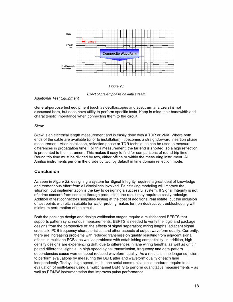
Figure 23.
Effect of pre-emphasis on data stream. Additional Test Equipment General-purpose test equipment (such as oscilloscopes and spectrum analyzers) is not discussed here, but does have utility to perform specific tests. Keep in mind their bandwidth and characteristic impedance when connecting them to the circuit. Skew Skew is an electrical length measurement and is easily done with a TDR or VNA. Where both ends of the cable are available (prior to installation), it becomes a straightforward insertion phase measurement. After installation, reflection phase or TDR techniques can be used to measure differences in propagation time. For this measurement, the far end is shorted, so a high reflection is presented to the instrument. This makes it easy to find for comparisons of round trip time. Round trip time must be divided by two, either offline or within the measuring instrument. All Anritsu instruments perform the divide by two, by default in time domain reflection mode. Conclusion As seen in Figure 23, designing a system for Signal Integrity requires a great deal of knowledge and tremendous effort from all disciplines involved. Painstaking modeling will improve the situation, but implementation is the key to designing a successful system. If Signal Integrity is not of prime concern from concept through production, the result may require a costly redesign. Addition of test connectors simplifies testing at the cost of additional real estate, but the inclusion of test points with pitch suitable for wafer probing makes for non-destructive troubleshooting with minimum perturbation of the circuit. Both the package design and design verification stages require a multichannel BERTS that supports pattern synchronous measurements. BERTS is needed to verify the logic and package designs from the perspective of: the effects of signal separation; wiring lengths; adjacent signal crosstalk; PCB frequency characteristics; and other aspects of output waveform quality. Currently, there are increasing problems with reduced transmission quality resulting from adjacent signal effects in multilane PCBs, as well as problems with establishing compatibility. In addition, high-density designs are experiencing drift, due to differences in lane wiring lengths, as well as drift in paired differential signals. In high-speed signal transmission, frequency and data-pattern dependencies cause worries about reduced waveform quality. As a result, it is no longer sufficient to perform evaluations by measuring the BER, jitter and waveform quality of each lane independently. Today’s high-speed, multi-lane serial communications standards require total evaluation of multi-lanes using a multichannel BERTS to perform quantitative measurements – as well as RF/MW instrumentation that improves pulse performance.

19
©Anritsu Signal Integrity Basics White Paper_2009-04134 -09