si826x - silicon labs mosfets and igbts used in a ... diode emulator model and i-v curve figure 2....
TRANSCRIPT

Rev. 1.4 12/17 Copyright © 2017 by Silicon Laboratories Si826x
Si826x
5 KV LED EMULATOR INPUT, 4.0 A ISOLATED GATE DRIVERS
Features
Applications
Safety Regulatory Approvals
Description
The Si826x isolators are pin-compatible, drop-in upgrades for popular opto-coupled gate drivers, such as 0.6 A ACPL-0302/3020, 2.5 A HCPL-3120/ACPL-3130, HCNW3120/3130, and similar opto-drivers. The devices are ideal for drivingpower MOSFETs and IGBTs used in a wide variety of inverter and motor controlapplications. The Si826x isolated gate drivers utilize Silicon Laboratories'proprietary silicon isolation technology, supporting up to 5.0 kVRMS withstandvoltage per UL1577 and 10kV surge protection per VDE 0884-10. This technologyenables higher-performance, reduced variation with temperature and age, tighterpart-to-part matching, and superior common-mode rejection compared to opto-coupled gate drivers. While the input circuit mimics the characteristics of an LED,less drive current is required, resulting in higher efficiency. Propagation delay timeis independent of input drive current, resulting in consistently short propagationtimes, tighter unit-to-unit variation, and greater input circuit design flexibility. As aresult, the Si826x series offers longer service life and dramatically higher reliabilitycompared to opto-coupled gate drivers.
Pin-compatible, drop-in upgrades for popular high speed opto-coupled gate drivers
Low power diode emulator simplifies design-in process
0.6 and 4.0 Amp peak output drive current
Rail-to-rail output voltage Performance and reliability
advantages vs. opto-driversResistant to temperature and age10x lower FIT rate for longer
service life14x tighter part-to-part matchingHigher common-mode transient
immunity: >50 kV/µs typical
Robust protection featuresMultiple UVLO ordering options
(5, 8, and 12 V) with hysteresis 60 ns propagation delay,
independent of input drive current Wide VDD range: 6.5 to 30 V
Up to 5000 VRMS isolation
10 kV surge withstand capability AEC-Q100 qualified Wide operating temperature range
–40 to +125 °C RoHS-compliant packages
SOIC-8 (Narrow body)DIP8 (Gull-wing)SDIP6 (Stretched SO-6)
IGBT/ MOSFET gate drives Industrial, HEV and renewable
energy inverters AC, Brushless, and DC motor
controls and drives
Variable speed motor control in consumer white goods
Isolated switch mode and UPS power supplies
UL 1577 recognizedUp to 5000 Vrms for 1 minute
CSA component notice 5A approvalIEC 60950-1, 60601-1
(reinforced insulation)
VDE certification conformityVDE0884-10
(basic/reinforced insulation) CQC certification approval
GB4943.1
Patent pending
Pin Assignments:
See page 23
1
2
3
4
8
7
6
5
ANODE
CATHODE
NC
VDD
VO
VO
SOIC-8, DIP8 Industry Standard Pinout
GND
UVLO
1
3
6
5
4
ANODE
CATHODE
VDD
VO
GND
SDIP6Industry Standard Pinout
2NC
UVLO
e
e

Si826x
2 Rev. 1.4
Functional Block Diagram
DiodeEmulator
IF
A1
OUT
VDD
XMIT
GND
REC
C1
Output Driver

Si826x
Rev. 1.4 3
TABLE OF CONTENTS
Section Page
1. Electrical Specifications . . . . . . . . . . . . . . . . . . . . . . . . . . . . . . . . . . . . . . . . . . . . . . . . . . .42. Regulatory Information . . . . . . . . . . . . . . . . . . . . . . . . . . . . . . . . . . . . . . . . . . . . . . . . . . . .93. Functional Description . . . . . . . . . . . . . . . . . . . . . . . . . . . . . . . . . . . . . . . . . . . . . . . . . . .15
3.1. Theory of Operation . . . . . . . . . . . . . . . . . . . . . . . . . . . . . . . . . . . . . . . . . . . . . . . . .154. Technical Description . . . . . . . . . . . . . . . . . . . . . . . . . . . . . . . . . . . . . . . . . . . . . . . . . . . .16
4.1. Device Behavior . . . . . . . . . . . . . . . . . . . . . . . . . . . . . . . . . . . . . . . . . . . . . . . . . . . .164.2. Device Startup . . . . . . . . . . . . . . . . . . . . . . . . . . . . . . . . . . . . . . . . . . . . . . . . . . . . . .164.3. Under Voltage Lockout (UVLO) . . . . . . . . . . . . . . . . . . . . . . . . . . . . . . . . . . . . . . . .17
5. Applications . . . . . . . . . . . . . . . . . . . . . . . . . . . . . . . . . . . . . . . . . . . . . . . . . . . . . . . . . . . .185.1. Input Circuit Design . . . . . . . . . . . . . . . . . . . . . . . . . . . . . . . . . . . . . . . . . . . . . . . . . .185.2. Output Circuit Design . . . . . . . . . . . . . . . . . . . . . . . . . . . . . . . . . . . . . . . . . . . . . . . .195.3. Layout Considerations . . . . . . . . . . . . . . . . . . . . . . . . . . . . . . . . . . . . . . . . . . . . . . .195.4. Power Dissipation Considerations . . . . . . . . . . . . . . . . . . . . . . . . . . . . . . . . . . . . . .20
6. Pin Descriptions (SOIC-8, DIP8) . . . . . . . . . . . . . . . . . . . . . . . . . . . . . . . . . . . . . . . . . . . .227. Pin Descriptions (SDIP6) . . . . . . . . . . . . . . . . . . . . . . . . . . . . . . . . . . . . . . . . . . . . . . . . . .238. Ordering Guide . . . . . . . . . . . . . . . . . . . . . . . . . . . . . . . . . . . . . . . . . . . . . . . . . . . . . . . . . .249. Package Outline: 8-Pin Narrow Body SOIC . . . . . . . . . . . . . . . . . . . . . . . . . . . . . . . . . . .2710. Land Pattern: 8-Pin Narrow Body SOIC . . . . . . . . . . . . . . . . . . . . . . . . . . . . . . . . . . . . .2811. Package Outline: DIP8 . . . . . . . . . . . . . . . . . . . . . . . . . . . . . . . . . . . . . . . . . . . . . . . . . . .2912. Land Pattern: DIP8 . . . . . . . . . . . . . . . . . . . . . . . . . . . . . . . . . . . . . . . . . . . . . . . . . . . . . .3013. Package Outline: SDIP6 . . . . . . . . . . . . . . . . . . . . . . . . . . . . . . . . . . . . . . . . . . . . . . . . . .3114. Land Pattern: SDIP6 . . . . . . . . . . . . . . . . . . . . . . . . . . . . . . . . . . . . . . . . . . . . . . . . . . . . .3315. Top Markings . . . . . . . . . . . . . . . . . . . . . . . . . . . . . . . . . . . . . . . . . . . . . . . . . . . . . . . . . .34
15.1. Si826x Top Marking (Narrow Body SOIC) . . . . . . . . . . . . . . . . . . . . . . . . . . . . . . .3415.2. Top Marking Explanation . . . . . . . . . . . . . . . . . . . . . . . . . . . . . . . . . . . . . . . . . . . .3415.3. Si826x Top Marking (DIP8) . . . . . . . . . . . . . . . . . . . . . . . . . . . . . . . . . . . . . . . . . . .3515.4. Top Marking Explanation . . . . . . . . . . . . . . . . . . . . . . . . . . . . . . . . . . . . . . . . . . . .3515.5. Si826x Top Marking (SDIP6) . . . . . . . . . . . . . . . . . . . . . . . . . . . . . . . . . . . . . . . . .3615.6. Top Marking Explanation . . . . . . . . . . . . . . . . . . . . . . . . . . . . . . . . . . . . . . . . . . . .36
Document Change List . . . . . . . . . . . . . . . . . . . . . . . . . . . . . . . . . . . . . . . . . . . . . . . . . . . . .37

Si826x
4 Rev. 1.4
1. Electrical Specifications
Table 1. Recommended Operating Conditions
Parameter Symbol Min Typ Max Unit
Supply Voltage VDD 6.5 — 30 V
Input Current IF(ON)(see Figure 1)
6 — 30 mA
Operating Temperature (Ambient) TA –40 — 125 °C
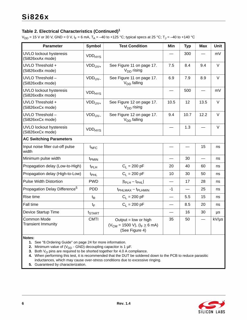
Table 2. Electrical Characteristics 1
VDD = 15 V or 30 V, GND = 0 V, IF = 6 mA, TA = –40 to +125 °C; typical specs at 25 °C; TJ = –40 to +140 °C
Parameter Symbol Test Condition Min Typ Max Unit
DC Parameters
Supply Voltage2 VDD (VDD – GND) 6.5 — 30 V
Supply Current (Output High) IDD
IF = 10 mAVDD = 15 VVDD = 30 V
——
1.82.0
2.42.7
mAmA
Supply Current (Output Low) IDD
VF = 0 V; IF = 0 mAVDD = 15 VVDD = 30 V
——
1.51.7
2.12.4
mAmA
Input Current Threshold IF(TH) — — 3.6 mA
Input Current Hysteresis IHYS — 0.34 — mA
Input Forward Voltage (OFF) VF(OFF) Measured at ANODE with respect to CATHODE.
— — 1 V
Input Forward Voltage (ON) VF(ON) Measured at ANODE with respect to CATHODE.
1.6 — 2.8 V
Input Capacitance CI f = 100 kHz,VF = 0 V,VF = 2 V
——
1515
——
pF
Output Resistance High (Source)3
ROH
Si826xAxx devices — 15 —
Si826xBxx devices (IOH = -1 A) — 2.6 5.1
Output Resistance Low (Sink)3 ROL
Si826xAxx devices — 5 —
Si826xBxx devices (IOL = 2 A) — 0.8 2.0
Notes:1. See "8.Ordering Guide" on page 24 for more information.2. Minimum value of (VDD - GND) decoupling capacitor is 1 µF.3. Both VO pins are required to be shorted together for 4.0 A compliance.4. When performing this test, it is recommended that the DUT be soldered down to the PCB to reduce parasitic
inductances, which may cause over-stress conditions due to excessive ringing.5. Guaranteed by characterization.

Si826x
Rev. 1.4 5
Output High Current (Source)3,4 IOH
Si826xAxx devices (IF = 0),(tPW_IOH < 250 ns)
(see Figure 3)— 0.4 —
ASi826xBxx devices (IF = 0),(tPW_IOH < 250 ns),(VDD – VO = 7.5 V)
(see Figure 3)0.5 1.8 —
Output Low Current (Sink)3,4 IOL
Si826xAxx devices (IF = 10 mA),
(tPW_IOL < 250 ns)(see Figure 2)
— 0.6 —
ASi826xBxx devices (IF = 10 mA),
(tPW_IOL < 250 ns),(VO - GND = 4.2 V)
(see Figure 2)
1.2 4.0 —
High-Level Output Voltage VOH
Si826xAxx devices(I OUT = –100 mA)
—VDD–0.4
—
VSi826xBxx devices(I OUT = –100 mA)
VDD–0.5
VDD–0.25 —
Si826xBxx devices(I OUT = 0 mA),
(IF = 0 mA)— VDD —
Low-Level Output Voltage VOL
Si826xAxx devices(I OUT = 100 mA),
(IF = 10 mA)— 320 —
mVSi826xBxx devices(I OUT = 100 mA),
(IF = 10 mA)— 80 200
UVLO Threshold + (Si826xxAx mode)
VDDUV+ See Figure 10 on page 17.VDD rising
5 5.6 6.3 V
UVLO Threshold – (Si826xxAx mode)
VDDUV– See Figure 10 on page 17.VDD falling
4.7 5.3 6.0 V
Table 2. Electrical Characteristics (Continued)1
VDD = 15 V or 30 V, GND = 0 V, IF = 6 mA, TA = –40 to +125 °C; typical specs at 25 °C; TJ = –40 to +140 °C
Parameter Symbol Test Condition Min Typ Max Unit
Notes:1. See "8.Ordering Guide" on page 24 for more information.2. Minimum value of (VDD - GND) decoupling capacitor is 1 µF.3. Both VO pins are required to be shorted together for 4.0 A compliance.4. When performing this test, it is recommended that the DUT be soldered down to the PCB to reduce parasitic
inductances, which may cause over-stress conditions due to excessive ringing.5. Guaranteed by characterization.
Si826x
6 Rev. 1.4
UVLO lockout hysteresis (Si826xxAx mode)
VDDHYS— 300 — mV
UVLO Threshold + (Si826xxBx mode)
VDDUV+ See Figure 11 on page 17.VDD rising
7.5 8.4 9.4 V
UVLO Threshold – (Si826xxBx mode)
VDDUV– See Figure 11 on page 17.VDD falling
6.9 7.9 8.9 V
UVLO lockout hysteresis (Si826xxBx mode)
VDDHYS— 500 — mV
UVLO Threshold + (Si826xxCx mode)
VDDUV+ See Figure 12 on page 17.VDD rising
10.5 12 13.5 V
UVLO Threshold – (Si826xxCx mode)
VDDUV– See Figure 12 on page 17.VDD falling
9.4 10.7 12.2 V
UVLO lockout hysteresis (Si826xxCx mode)
VDDHYS— 1.3 — V
AC Switching Parameters
Input noise filter cut-off pulse width
tNFC — — 15 ns
Minimum pulse width tPMIN — 30 — ns
Propagation delay (Low-to-High) tPLH CL = 200 pF 20 40 60 ns
Propagation delay (High-to-Low) tPHL CL = 200 pF 10 30 50 ns
Pulse Width Distortion PWD |tPLH – tPHL| — 17 28 ns
Propagation Delay Difference5 PDD tPHLMAX – tPLHMIN -1 — 25 ns
Rise time tR CL = 200 pF — 5.5 15 ns
Fall time tF CL = 200 pF — 8.5 20 ns
Device Startup Time tSTART — 16 30 µs
Common Mode Transient Immunity
CMTI Output = low or high(VCM = 1500 V), (IF > 6 mA)
(See Figure 4)
35 50 — kV/µs
Table 2. Electrical Characteristics (Continued)1
VDD = 15 V or 30 V, GND = 0 V, IF = 6 mA, TA = –40 to +125 °C; typical specs at 25 °C; TJ = –40 to +140 °C
Parameter Symbol Test Condition Min Typ Max Unit
Notes:1. See "8.Ordering Guide" on page 24 for more information.2. Minimum value of (VDD - GND) decoupling capacitor is 1 µF.3. Both VO pins are required to be shorted together for 4.0 A compliance.4. When performing this test, it is recommended that the DUT be soldered down to the PCB to reduce parasitic
inductances, which may cause over-stress conditions due to excessive ringing.5. Guaranteed by characterization.

Si826x
Rev. 1.4 7
Figure 1. Diode Emulator Model and I-V Curve
Figure 2. IOL Sink Current Test Circuit
0.0
0.5
1.0
1.5
2.0
2.5
3.0
0 5 10 15 20 25 30
Anod
eto
Cathod
eVo
ltage
[V]
Diode Emulator Input Current [mA]
700 2.2 V
10
Anode
Cathode
ESD
Anode
Cathode
e
INPUT
1 µF 100 µF
10
RSNS0.1
Si826x
1 µFCER
10 µFEL
VDD = 15 V
IN OUT
GND
VDD
SCHOTTKY
50 ns
200 ns
Measure
INPUT WAVEFORM
GND
IF
9 V+_

Si826x
8 Rev. 1.4
Figure 3. IOH Source Current Test Circuit
Figure 4. Common Mode Transient Immunity Characterization Circuit
INPUT
1 µF 100 µF
10
RSNS0.1
Si826x
1 µFCER
10 µFEL
VDD = 15 V
IN OUT
VSS
VDD
50 ns
200 ns
Measure
INPUT WAVEFORM
GND
IF
SCHOTTKY5.5 V
+_
Oscilloscope
5 VIsolated Supply
VO
15 VSupply
High Voltage Surge Generator
Vcm SurgeOutput
High Voltage Differential
Probe
GNDCathode
AnodeInput SignalSwitch
InputOutput
Isolated Ground
267Si826x
VDD

Si826x
Rev. 1.4 9
2. Regulatory Information
Table 3. Regulatory Information*
CSA
The Si826x is certified under CSA Component Acceptance Notice 5A. For more details, see Master Contract Number 232873.
60950-1: Up to 1000 VRMS reinforced insulation working voltage; up to 1000 VRMS basic insulation working voltage.
60601-1: Up to 250 VRMS working voltage and 2 MOPP (Means of Patient Protection).
VDE
The Si826x is certified according to VDE0884-10. For more details, see certificate 40037519.
VDE0884 Part 10: Up to 1414 Vpeak for reinforced insulation working voltage.
UL
The Si826x is certified under UL1577 component recognition program. For more details, see File E257455.
Rated up to 5000 VRMS isolation voltage for basic protection.
CQC
The Si826x is certified under GB4943.1-2011. For more details, see certificates CQC15001121282 and CQC15001121283.
Rated up to 1000 VRMS reinforced insulation working voltage; up to 1000 VRMS basic insulation working voltage.
*Note: Regulatory Certifications apply to 3.75 kVRMS rated devices which are production tested to 4.5 kVRMS for 1 sec.Regulatory Certifications apply to 5.0 kVRMS rated devices which are production tested to 6.0 kVRMS for 1 sec.For more information, see "8.Ordering Guide" on page 24.
Table 4. Insulation and Safety-Related Specifications
Parameter Symbol Test ConditionValue
UnitSOIC-8 DIP8 SDIP6
Nominal External Air Gap(Clearance)
CLR 4.7 min 7.2 min 9.6 min mm
Nominal External Tracking(Creepage)
CPG 3.9 min 7.0 min 8.3 min mm
Minimum Internal Gap(Internal Clearance)
DTI 0.016 0.016 0.016 mm
Tracking ResistanceCTI or
PTIIEC60112 600 600 600 V
Erosion Depth ED 0.031 0.031 0.057 mm
Resistance (Input-Output)* RIO 1012 1012 1012
Capacitance (Input-Output)* CIO f = 1 MHz 1 1 1 pF
*Note: To determine resistance and capacitance, the Si826x is converted into a 2-terminal device. Pins 1–4 (1–3, SDIP6) are shorted together to form the first terminal, and pins 5–8 (4–6, SDIP6) are shorted together to form the second terminal. The parameters are then measured between these two terminals.

Si826x
10 Rev. 1.4
Table 5. IEC 60664-1 Ratings
Parameter Test ConditionsSpecification
SOIC-8 DIP8 SDIP6
Basic Isolation Group Material Group I I I
Installation Classification
Rated Mains Voltages < 150 VRMS
I-IV I-IV I-IV
Rated Mains Voltages < 300 VRMS
I-IV I-IV I-IV
Rated Mains Voltages < 450 VRMS
I-III I-III I-IV
Rated Mains Voltages < 600 VRMS
I-III I-III I-IV
Rated Mains Voltages < 1000 VRMS
I-II I-II I-III
Table 6. VDE 0884-10 Insulation Characteristics*
Parameter Symbol Test ConditionCharacteristic
UnitSOIC-8 DIP8 SDIP6
Maximum WorkingInsulation Voltage
VIORM630 891 1140 V peak
Input to Output Test Voltage
VPR
Method b1(VIORM x 1.875 = VPR, 100%Production Test, tm = 1 sec,Partial Discharge < 5 pC)
1181 1671 2138 V peak
Transient Overvoltage VIOTM t = 60 sec 6000 6000 8000 V peak
Surge Voltage VIOSM
Tested per IEC 60065 with surge voltage of 1.2 μs/50 μs Si826x tested with magnitude 6250 V x 1.6 = 10 kV
6250 6250 6250 V peak
Pollution Degree (DIN VDE 0110, Table 1)
2 2 2
Insulation Resistance at TS, VIO = 500 V
RS>109 >109 >109
*Note: This isolator is suitable for reinforced electrical isolation only within the safety limit data. Maintenance of the safety data is ensured by protective circuits. The Si826x provides a climate classification of 40/125/21.

Si826x
Rev. 1.4 11
Table 7. IEC Safety Limiting Values*
Parameter Symbol Test ConditionMax
UnitSOIC-8 DIP8 SDIP6
Case Temperature TS 140 140 140 °C
Input Current IS
JA = 110 °C/W (SOIC-8), 110 °C/W (DIP8),
105 °C/W (SDIP6), VF = 2.8 V, TJ = 140 °C,
TA = 25 °C
370 370 390 mA
Output Power PS 1 1 1 W
*Note: Maximum value allowed in the event of a failure; also see the thermal derating curve in Figures 5, 6, 7, and 8.

Si826x
12 Rev. 1.4
Figure 5. (SOIC-8) Thermal Derating Curve, Dependence of Safety Limiting Valueswith Case Temperature per VDE0884-10
Figure 6. (DIP8) Thermal Derating Curve, Dependence of Safety Limiting Valueswith Case Temperature per VDE0884-10
Table 8. Thermal Characteristics
Parameter SymbolTyp
UnitSOIC-8 DIP8 SDIP6
IC Junction-to-Air Thermal Resistance
JA 110 110 105 ºC/W
400
600
800
1000
1200
ower
Ps,Inp
utCu
rren
tIs
Ps (mW)
Is (mA)
0
200
0 20 40 60 80 100 120 140
Outpu
tPo
Ts Case Temperature (°C)
400
600
800
1000
1200
ower
Ps,Inp
utCu
rren
tIs
Ps (mW)
Is (mA)
0
200
0 20 40 60 80 100 120 140
Outpu
tPo
Ts Case Temperature (°C)

Si826x
Rev. 1.4 13
Figure 7. (SDIP6) Thermal Derating Curve, Dependence of Safety Limiting Valueswith Case Temperature per VDE0884-10
400
600
800
1000
1200ow
erPs,Inp
utCu
rren
tIs
Ps (mW)
Is (mA)
0
200
0 20 40 60 80 100 120 140
Outpu
tPo
Ts Case Temperature (°C)

Si826x
14 Rev. 1.4
Table 9. Absolute Maximum Ratings*
Parameter Symbol Min Max Unit
Storage Temperature TSTG –65 +150 °C
Operating Temperature TA –40 +125 °C
Junction Temperature TJ — +140 °C
Average Forward Input Current IF(AVG) — 30 mA
Peak Transient Input Current (< 1 µs pulse width, 300 ps)
IFTR — 1 A
Reverse Input Voltage VR — 0.3 V
Supply Voltage VDD –0.5 36 V
Output Voltage VOUT –0.5 36 V
Peak Output Current (tPW = 10 µs, duty cycle = 0.2%) (0.6 Amp versions)
IOPK — 0.6 A
Peak Output Current (tPW = 10 µs, duty cycle = 0.2%) (4.0 Amp versions)
IOPK — 4.0 A
Input Power Dissipation PI — 75 mW
Output Power Dissipation PO — 225 mW
Total Power Dissipation (all packages limited by thermal derating curve)
PT — 300 mW
Lead Solder Temperature (10 s) — 260 °C
HBM Rating ESD 4 — kV
Machine Model ESD 300 — V
CDM 2000 — V
Maximum Isolation Voltage (1 s) SOIC-8 — 4500 VRMS
Maximum Isolation Voltage (1 s) DIP8 — 6500 VRMS
Maximum Isolation Voltage (1 s) SDIP6 — 6500 VRMS
*Note: Permanent device damage may occur if the absolute maximum ratings are exceeded. Functional operation should be restricted to the conditions specified in the operational sections of this data sheet.
Si826x
Rev. 1.4 15
3. Functional Description
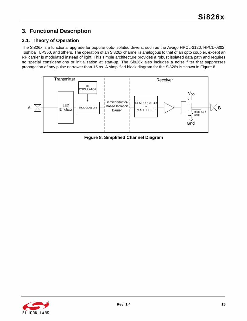
3.1. Theory of OperationThe Si826x is a functional upgrade for popular opto-isolated drivers, such as the Avago HPCL-3120, HPCL-0302,Toshiba TLP350, and others. The operation of an Si826x channel is analogous to that of an opto coupler, except anRF carrier is modulated instead of light. This simple architecture provides a robust isolated data path and requiresno special considerations or initialization at start-up. The Si826x also includes a noise filter that suppressespropagation of any pulse narrower than 15 ns. A simplified block diagram for the Si826x is shown in Figure 8.
Figure 8. Simplified Channel Diagram
RF OSCILLATOR
MODULATOR
DEMODULATOR+
NOISE FILTERA B
Semiconductor-Based Isolation
Barrier
Transmitter Receiver
LED Emulator
0.6 to 4.0 A peak
Gnd
VDD
Si826x
16 Rev. 1.4
4. Technical Description
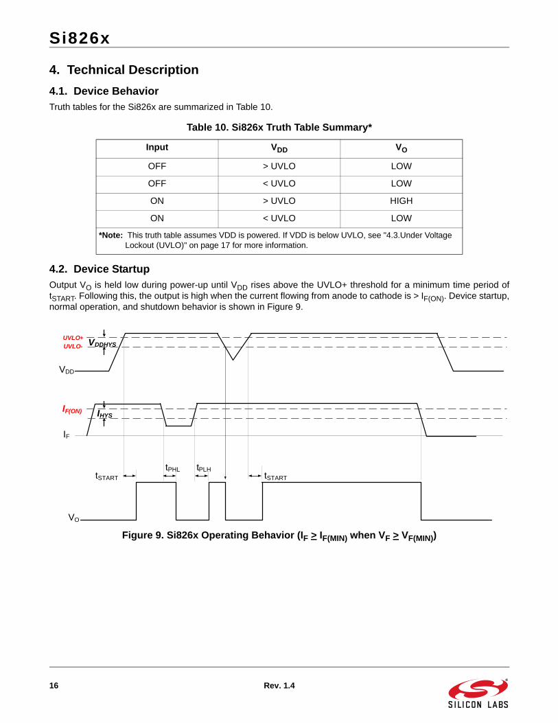
4.1. Device BehaviorTruth tables for the Si826x are summarized in Table 10.
4.2. Device StartupOutput VO is held low during power-up until VDD rises above the UVLO+ threshold for a minimum time period oftSTART. Following this, the output is high when the current flowing from anode to cathode is > IF(ON). Device startup,normal operation, and shutdown behavior is shown in Figure 9.
Figure 9. Si826x Operating Behavior (IF > IF(MIN) when VF > VF(MIN))
Table 10. Si826x Truth Table Summary*
Input VDD VO
OFF > UVLO LOW
OFF < UVLO LOW
ON > UVLO HIGH
ON < UVLO LOW
*Note: This truth table assumes VDD is powered. If VDD is below UVLO, see "4.3.Under Voltage Lockout (UVLO)" on page 17 for more information.
IF
VO
VDD
tSTART tSTART
VDDHYS
tPHL tPLH
IF(ON)
UVLO+UVLO-
IHYS

Si826x
Rev. 1.4 17
4.3. Under Voltage Lockout (UVLO)The UVLO circuit unconditionally drives VO low when VDD is below the lockout threshold. Referring to Figures 10through 12, upon power up, the Si826x is maintained in UVLO until VDD rises above VDDUV+. During power down,the Si826x enters UVLO when VDD falls below the UVLO threshold plus hysteresis (i.e., VDD < VDDUV+ –VDDHYS).
Figure 10. Si826xxAx UVLO Response (5 V)
Figure 11. Si826xxBX UVLO Response (8 V)
Figure 12. Si826xxCx UVLO Response (12 V)
3.5
VDDUV+ (Typ)
Ou
tpu
t V
olt
age
(VO)
4.0 4.5 5.0 5.5 6.0 6.5 7.0 7.5
Supply Voltage (VDD - GND) (V)
6.0
VDDUV+ (Typ)
Ou
tpu
t V
olt
ag
e (
VO)
6.5 7.0 7.5 8.0 8.5 9.0 9.5 10.0
Supply Voltage (VDD - GND) (V)
9.5
VDDUV+ (Typ)
Ou
tpu
t V
olt
age
(VO)
10.0 10.5 11.0 11.5 12.0 12.5 13.0
Supply Voltage (VDD - GND) (V)

Si826x
18 Rev. 1.4
5. Applications
The following sections detail the input and output circuits necessary for proper operation. Power dissipation andlayout considerations are also discussed.
5.1. Input Circuit DesignOpto driver manufacturers typically recommend the circuits shown in Figures 13 and 14. These circuits arespecifically designed to improve opto-coupler input common-mode rejection and increase noise immunity.
Figure 13. Si826x Input Circuit
Figure 14. High CMR Si826x Input Circuit
The optically-coupled driver circuit of Figure 13 turns the LED on when the control input is high. However, internalcapacitive coupling from the LED to the power and ground conductors can momentarily force the LED into its offstate when the anode and cathode inputs are subjected to a high common-mode transient. The circuit shown inFigure 14 addresses this issue by using a value of R1 sufficiently low to overdrive the LED, ensuring it remains onduring an input common-mode transient. Q1 shorts the LED off in the low output state, again increasing common-mode transient immunity.
Some opto driver applications recommend reverse-biasing the LED when the control input is off to prevent couplednoise from energizing the LED. The Si826x input circuit requires less current and has twice the off-state noisemargin compared to opto couplers. However, high CMR opto coupler designs that overdrive the LED (seeFigure 14) may require increasing the value of R1 to limit input current IF to its maximum rating when using theSi826x. In addition, there is no benefit in driving the Si826x input diode into reverse bias when in the off state.
R11
2
3
4
Si826xVext
Open Drain or Collector
Control Input
ANODE
CATHODE
N/C
N/C
R1
1
2
3
4
Si826xVext
Control Input
ANODE
CATHODE
N/C
N/C
Q1

Si826x
Rev. 1.4 19
Consequently, opto coupler circuits using this technique should either leave the negative bias circuitry unpopulatedor modify the circuitry (e.g., add a clamp diode or current limiting resistor) to ensure that the anode pin of theSi826x is no more than –0.3 V with respect to the cathode when reverse-biased.
New designs should consider the input circuit configurations of Figure 15, which are more efficient than those ofFigures 13 and 14. As shown, S1 and S2 represent any suitable switch, such as a BJT or MOSFET, analogtransmission gate, processor I/O, etc. Also, note that the Si826x input can be driven from the I/O port of any MCUor FPGA capable of sourcing a minimum of 6 mA (see Figure 15C). Additionally, note that the Si826x propagationdelay and output drive do not significantly change for values of IF between IF(MIN) and IF(MAX).
Figure 15. Si826x Other Input Circuit Configurations
5.2. Output Circuit DesignGND can be biased at, above, or below ground as long as the voltage on VDD with respect to GND is a maximumof 30 V. VDD decoupling capacitors should be placed as close to the package pins as possible. The optimumvalues for these capacitors depend on load current and the distance between the chip and its power source. It isrecommended that 0.1 and 10 µF bypass capacitors be used to reduce high-frequency noise and maximizeperformance.
5.3. Layout ConsiderationsIt is most important to minimize ringing in the drive path and noise on the VDD lines. Care must be taken tominimize parasitic inductance in these paths by locating the Si826x as close as possible to the device it is driving.In addition, the VDD supply and ground trace paths must be kept short. For this reason, the use of power andground planes is highly recommended. A split ground plane system having separate ground and VDD planes forpower devices and small signal components provides the best overall noise performance.
Control Input
Vext
R1
S1
N/C
ANODE
CATHODE
N/CSee Text
Si826x
A
4
3
2
1
Si826x
1
2
3
4
Vext
Control Input
S1 N/C
ANODE
CATHODE
N/C
B
R1
S2
Si826x
C
4 N/C
3 CATHODE
2MCU I/O Port pin
ANODER1
1 N/C

Si826x
20 Rev. 1.4
5.4. Power Dissipation ConsiderationsProper system design must assure that the Si826x operates within safe thermal limits across the entire load range.The Si826x total power dissipation is the sum of the power dissipated by bias supply current, internal switchinglosses, and power delivered to the load, as shown in Equation 1.
Equation 1.
The maximum allowable power dissipation for the Si826x is a function of the package thermal resistance, ambienttemperature, and maximum allowable junction temperature, as shown in Equation 2.
Equation 2.
Substituting values for PDmax Tjmax, TA, and ja into Equation 2 results in a maximum allowable total powerdissipation of 1.0 W. Note that the maximum allowable load is found by substituting this limit and the appropriatedatasheet values from Table 2 on page 4 into Equation 1 and simplifying. Graphs are shown in Figures 16 and 18.All points along the load lines in these graphs represent the package dissipation-limited value of CL for thecorresponding switching frequency.
PD IF VF DC VDD+ IDDQ Qd CL+ VDD + f
where: PD is the total device power dissipation (W)
IF is the diode current (30 mA max)
VF is the diode anode to cathode voltage (2.8 V max)
DC is duty cycle (0.5 typical)
VDD is the driver-side supply voltage (30 V max)
IDDQ is the driver maximum bias current (2.5 mA)
Qd is 3 nC
CL is the load capacitance
f is the switching frequency (Hz)
=
PDmax
Tjmax TA–
ja---------------------------
where:
PDmax is the maximum allowable power dissipation (W)
Tjmax is the maximum junction temperature (140 °C)
TA is the ambient temperature (°C)
ja is the package junction-to-air thermal resistance (110 °C/W)

Si826x
Rev. 1.4 21
Figure 16. (SOIC-8, DIP8, SDIP6) Maximum Load vs. Switching Frequency (25 °C)
0.1
1.0
10.0
100.0
1000.0
10000.0
10 100 1000
Max
Load
(nF)
Frequency (kHz)
7V
12V
18V
30V

Si826x
22 Rev. 1.4
6. Pin Descriptions (SOIC-8, DIP8)
Figure 17. Pin Configuration
Table 11. Pin Descriptions (SOIC-8, DIP8)
Pin Name Description
1 NC* No connect.
2 ANODE Anode of LED emulator. VO follows the signal applied to this input with respect to the CATHODE input.
3 CATHODE Cathode of LED emulator. VO follows the signal applied to ANODE with respect to this input.
4 NC* No connect.
5 GND External MOSFET source connection and ground reference for VDD. This terminal is typically connected to ground but may be tied to a negative or positive voltage.
6 VO Output signal. Both VO pins are required to be shorted together for 4.0 A compliance.
7 VO Output signal. Both VO pins are required to be shorted together for 4.0 A compliance.
8 VDD Output-side power supply input referenced to GND (30 V max).
*Note: No Connect. These pins are not internally connected. To maximize CMTI performance, these pins should be connected to the ground plane.
1
2
3
4
8
7
6
5
NC
ANODE
CATHODE
NC
VDD
VO
VO
SOIC-8, DIP8 Industry Standard Pinout
GND
UVLO
e

Si826x
Rev. 1.4 23
7. Pin Descriptions (SDIP6)
Figure 18. Pin Configuration
Table 12. Pin Descriptions (SDIP6)
Pin Name Description
1 ANODE Anode of LED emulator. VO follows the signal applied to this input with respect to the CATHODE input.
2 NC* No connect.
3 CATHODE Cathode of LED emulator. VO follows the signal applied to ANODE with respect to this input.
4 GND External MOSFET source connection and ground reference for VDD. This terminal is typically connected to ground but may be tied to a negative or positive voltage.
5 VO Output signal.
6 VDD Output-side power supply input referenced to GND (30 V max).
*Note: No Connect. These pins are not internally connected. To maximize CMTI performance, these pins should be connected to the ground plane.
1
3
6
5
4
ANODE
CATHODE
VDD
VO
GND
SDIP6Industry Standard Pinout
2NC
UVLO
e

Si826x
24 Rev. 1.4
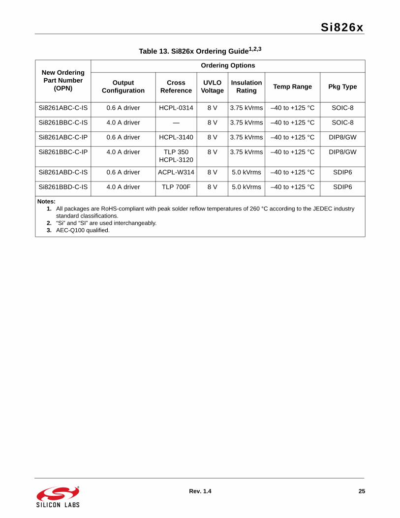
8. Ordering Guide
Table 13. Si826x Ordering Guide1,2,3
New Ordering Part Number
(OPN)
Ordering Options
Output Configuration
Cross Reference
UVLO Voltage
Insulation Rating
Temp Range Pkg Type
Si8261AAC-C-IS 0.6 A driver HCPL-0314 5 V 3.75 kVrms –40 to +125 °C SOIC-8
Si8261BAC-C-IS 4.0 A driver — 5 V 3.75 kVrms –40 to +125 °C SOIC-8
Si8261AAC-C-IP 0.6 A driver HCPL-3140 5 V 3.75 kVrms –40 to +125 °C DIP8/GW
Si8261BAC-C-IP 4.0 A driver TLP 350HCPL-3120
5 V 3.75 kVrms –40 to +125 °C DIP8/GW
Si8261AAD-C-IS 0.6 A driver ACPL-W314 5 V 5.0 kVrms –40 to +125 °C SDIP6
Si8261BAD-C-IS 4.0 A driver TLP 700F 5 V 5.0 kVrms –40 to +125 °C SDIP6
Notes:1. All packages are RoHS-compliant with peak solder reflow temperatures of 260 °C according to the JEDEC industry
standard classifications.2. “Si” and “SI” are used interchangeably.3. AEC-Q100 qualified.
Si826x
Rev. 1.4 25
Si8261ABC-C-IS 0.6 A driver HCPL-0314 8 V 3.75 kVrms –40 to +125 °C SOIC-8
Si8261BBC-C-IS 4.0 A driver — 8 V 3.75 kVrms –40 to +125 °C SOIC-8
Si8261ABC-C-IP 0.6 A driver HCPL-3140 8 V 3.75 kVrms –40 to +125 °C DIP8/GW
Si8261BBC-C-IP 4.0 A driver TLP 350HCPL-3120
8 V 3.75 kVrms –40 to +125 °C DIP8/GW
Si8261ABD-C-IS 0.6 A driver ACPL-W314 8 V 5.0 kVrms –40 to +125 °C SDIP6
Si8261BBD-C-IS 4.0 A driver TLP 700F 8 V 5.0 kVrms –40 to +125 °C SDIP6
Table 13. Si826x Ordering Guide1,2,3
New Ordering Part Number
(OPN)
Ordering Options
Output Configuration
Cross Reference
UVLO Voltage
Insulation Rating
Temp Range Pkg Type
Notes:1. All packages are RoHS-compliant with peak solder reflow temperatures of 260 °C according to the JEDEC industry
standard classifications.2. “Si” and “SI” are used interchangeably.3. AEC-Q100 qualified.

Si826x
26 Rev. 1.4
Si8261ACC-C-IS 0.6 A driver HCPL-0314 12 V 3.75 kVrms –40 to +125 °C SOIC-8
Si8261BCC-C-IS 4.0 A driver — 12 V 3.75 kVrms –40 to +125 °C SOIC-8
Si8261ACC-C-IP 0.6 A driver HCPL-3140 12 V 3.75 kVrms –40 to +125 °C DIP8/GW
Si8261BCC-C-IP 4.0 A driver TLP 350HCPL-3120
12 V 3.75 kVrms –40 to +125 °C DIP8/GW
Si8261ACD-C-IS 0.6 A driver ACPL-W314 12 V 5.0 kVrms –40 to +125 °C SDIP6
Si8261BCD-C-IS 4.0 A driver TLP 700F 12 V 5.0 kVrms –40 to +125 °C SDIP6
Table 13. Si826x Ordering Guide1,2,3
New Ordering Part Number
(OPN)
Ordering Options
Output Configuration
Cross Reference
UVLO Voltage
Insulation Rating
Temp Range Pkg Type
Notes:1. All packages are RoHS-compliant with peak solder reflow temperatures of 260 °C according to the JEDEC industry
standard classifications.2. “Si” and “SI” are used interchangeably.3. AEC-Q100 qualified.

Si826x
Rev. 1.4 27
9. Package Outline: 8-Pin Narrow Body SOIC
Figure 19 illustrates the package details for the Si826x in an 8-pin narrow-body SOIC package. Table 14 lists thevalues for the dimensions shown in the illustration.
Figure 19. 8-Pin Narrow Body SOIC Package
Table 14. 8-Pin Narrow Body SOIC Package Diagram Dimensions
SymbolMillimeters
Min Max
A 1.35 1.75
A1 0.10 0.25
A2 1.40 REF 1.55 REF
B 0.33 0.51
C 0.19 0.25
D 4.80 5.00
E 3.80 4.00
e 1.27 BSC
H 5.80 6.20
h 0.25 0.50
L 0.40 1.27
0 8

Si826x
28 Rev. 1.4
10. Land Pattern: 8-Pin Narrow Body SOIC
Figure 20 illustrates the recommended land pattern details for the Si826x in an 8-pin narrow-body SOIC. Table 15lists the values for the dimensions shown in the illustration.
Figure 20. 8-Pin Narrow Body SOIC Land Pattern
Table 15. 8-Pin Narrow Body SOIC Land Pattern Dimensions
Dimension Feature (mm)
C1 Pad Column Spacing 5.40
E Pad Row Pitch 1.27
X1 Pad Width 0.60
Y1 Pad Length 1.55
Notes:1. This Land Pattern Design is based on IPC-7351 pattern SOIC127P600X173-8N for
Density Level B (Median Land Protrusion).2. All feature sizes shown are at Maximum Material Condition (MMC) and a card
fabrication tolerance of 0.05 mm is assumed.

Si826x
Rev. 1.4 29
11. Package Outline: DIP8
Figure 21 illustrates the package details for the Si826x in a DIP8 package. Table 16 lists the values for thedimensions shown in the illustration.
Figure 21. DIP8 Package
Table 16. DIP8 Package Diagram Dimensions
Dimension Min Max
A — 4.19
A1 0.55 0.75
A2 3.17 3.43
b 0.35 0.55
b2 1.14 1.78
b3 0.76 1.14
c 0.20 0.33
D 9.40 9.90
E 7.37 7.87
E1 6.10 6.60
E2 9.40 9.90
e 2.54 BSC.
L 0.38 0.89
aaa — 0.25
Notes:1. All dimensions shown are in millimeters (mm) unless otherwise noted.2. Dimensioning and Tolerancing per ANSI Y14.5M-1994.

Si826x
30 Rev. 1.4
12. Land Pattern: DIP8
Figure 22 illustrates the recommended land pattern details for the Si826x in a DIP8 package. Table 17 lists thevalues for the dimensions shown in the illustration.
Figure 22. DIP8 Land Pattern
Table 17. DIP8 Land Pattern Dimensions*
Dimension Min Max
C 8.85 8.90
E 2.54 BSC
X 0.60 0.65
Y 1.65 1.70
*Note: This Land Pattern Design is based on the IPC-7351 specification.

Si826x
Rev. 1.4 31
13. Package Outline: SDIP6
Figure 23 illustrates the package details for the Si826x in an SDIP6 package. Table 18 lists the values for thedimensions shown in the illustration.
Figure 23. SDIP6 Package
Table 18. SDIP6 Package Diagram Dimensions
Dimension Min Max
A — 2.65
A1 0.10 0.30
A2 2.05 —
b 0.31 0.51
c 0.20 0.33
D 4.58 BSC
E 11.50 BSC
E1 7.50 BSC
e 1.27 BSC
Notes:1. All dimensions shown are in millimeters (mm) unless otherwise noted.2. Dimensioning and Tolerancing per ANSI Y14.5M-1994.

Si826x
32 Rev. 1.4
L 0.40 1.27
h 0.25 0.75
θ 0° 8°
aaa — 0.10
bbb — 0.33
ccc — 0.10
ddd — 0.25
eee — 0.10
fff — 0.20
Table 18. SDIP6 Package Diagram Dimensions (Continued)
Dimension Min Max
Notes:1. All dimensions shown are in millimeters (mm) unless otherwise noted.2. Dimensioning and Tolerancing per ANSI Y14.5M-1994.

Si826x
Rev. 1.4 33
14. Land Pattern: SDIP6
Figure 24 illustrates the recommended land pattern details for the Si826x in an SDIP6 package. Table 19 lists thevalues for the dimensions shown in the illustration.
Figure 24. SDIP6 Land Pattern
Table 19. SDIP6 Land Pattern Dimensions*
Dimension Min Max
C 10.45 10.50
E 1.27 BSC
X 0.55 0.60
Y 2.00 2.05
*Note: This Land Pattern Design is based on the IPC-7351 specification.

Si826x
34 Rev. 1.4
15. Top Markings
15.1. Si826x Top Marking (Narrow Body SOIC)
15.2. Top Marking Explanation
Line 1 Marking:
Customer Part Number 826 = ISOdriver product seriesC = Input configuration
1 = Opto input typeI = Peak output current
A = 0.6 A; B = 4.0 AU = UVLO level A = 5 V; B = 8 V; C = 12 VV = Isolation rating
C = 3.75 kV; D = 5.0 kV
Line 2 Marking:RTTTTT = Mfg Code Manufacturing Code from the Assembly Purchase
Order form.“R” indicates revision.
Line 3 Marking:
Circle = 43 mils DiameterLeft-Justified
“e4” Pb-Free Symbol
YY = YearWW = Work Week
Assigned by the Assembly House. Corresponds to the year and work week of the mold date.

Si826x
Rev. 1.4 35
15.3. Si826x Top Marking (DIP8)
15.4. Top Marking Explanation
Line 1 Marking:
Customer Part Number Si826 = ISOdriver product seriesC = Input configuration
1 = Opto input typeI = Peak output current
A = 0.6 A; B = 4.0 AU = UVLO level A = 5 V; B = 8 V; C = 12 VV = Isolation rating
C = 3.75 kV; D = 5.0 kV
Line 2 Marking:
YY = YearWW = Work Week
Assigned by the Assembly House. Corresponds to the year and work week of the mold date.
RTTTTT = Mfg Code Manufacturing Code from the Assembly Purchase Order form.“R” indicates revision.
Line 3 Marking:
Circle = 51 mils DiameterCenter-Justified
“e4” Pb-Free Symbol
CO = Country of Origin Country of OriginISO Code Abbreviation

Si826x
36 Rev. 1.4
15.5. Si826x Top Marking (SDIP6)
15.6. Top Marking Explanation
Line 1 Marking:Device Si826 = ISOdriver product series
C = Input configuration1 = Opto input type
Line 2 Marking:
Device Rating I = Peak output currentA = 0.6 A; B = 4.0 A
U = UVLO level A = 5 V; B = 8 V; C = 12 VV = Isolation rating
C = 3.75 kV; D = 5.0 kV
Line 3 Marking:RTTTTT = Mfg Code Manufacturing Code from the Assembly Purchase
Order form. “R” indicates revision.
Line 4 Marking: YY = YearWW = Work Week
Assigned by the Assembly House. Corresponds to the year and work week of the mold date.

Si826x
Rev. 1.4 37
DOCUMENT CHANGE LIST
Revision 0.9 to Revision 1.0 Updated Table 2 on page 4.
Added Figure 1 on page 7.
Updated "3.1.Theory of Operation" on page 15.
Updated Figures 10, 11, and 12 on page 17.
Removed “5.5. Parametric Differences between Si826x and HCPL-0302 and HCPL-3120 Opto Drivers”.
Revision 1.0 to Revision 1.1 Updated Figure 1 on page 7.
Updated Ordering Guide Table 13 on page 24.Removed references to moisture sensitivity levels from
table note.
Revision 1.1 to Revision 1.2 Removed “Sampling” from Ordering Guide Table 13
on page 24.
Revision 1.2 to Revision 1.3 Updated Table 3 on page 9.
Added CQC certificate numbers.
Updated Table 5 on page 10.Updated Rated Mains Voltage for 1000 VRMS ratings.
Updated Table 6 on page 10.Removed VIOSM specification.
Updated Table 9 on page 14.Replaced IO with Peak Output Current IOPK.
Updated Figure 13 on page 18.
Updated Figure 14 on page 18.
Updated Figure 15 on page 19.
Changed VDD minimum throughout document to reflect 6.5 V, not 5 V, as normal operation.
Revision 1.3 to Revision 1.4 Removed references to LGA8 throughout.
Deleted all IEC 60747-5 and IEC 61010 references throughout and added VDE 0884-10 references throughout.
Updated all certification body’s certificate and file reference numbers throughout.

http://www.silabs.com
Silicon Laboratories Inc.400 West Cesar ChavezAustin, TX 78701USA
Smart. Connected. Energy-Friendly.
Productswww.silabs.com/products
Qualitywww.silabs.com/quality
Support and Communitycommunity.silabs.com
DisclaimerSilicon Labs intends to provide customers with the latest, accurate, and in-depth documentation of all peripherals and modules available for system and software implementers using or intending to use the Silicon Labs products. Characterization data, available modules and peripherals, memory sizes and memory addresses refer to each specific device, and "Typical" parameters provided can and do vary in different applications. Application examples described herein are for illustrative purposes only. Silicon Labs reserves the right to make changes without further notice and limitation to product information, specifications, and descriptions herein, and does not give warranties as to the accuracy or completeness of the included information. Silicon Labs shall have no liability for the consequences of use of the information supplied herein. This document does not imply or express copyright licenses granted hereunder to design or fabricate any integrated circuits. The products are not designed or authorized to be used within any Life Support System without the specific written consent of Silicon Labs. A "Life Support System" is any product or system intended to support or sustain life and/or health, which, if it fails, can be reasonably expected to result in significant personal injury or death. Silicon Labs products are not designed or authorized for military applications. Silicon Labs products shall under no circumstances be used in weapons of mass destruction including (but not limited to) nuclear, biological or chemical weapons, or missiles capable of delivering such weapons.
Trademark InformationSilicon Laboratories Inc.® , Silicon Laboratories®, Silicon Labs®, SiLabs® and the Silicon Labs logo®, Bluegiga®, Bluegiga Logo®, Clockbuilder®, CMEMS®, DSPLL®, EFM®, EFM32®, EFR, Ember®, Energy Micro, Energy Micro logo and combinations thereof, "the world’s most energy friendly microcontrollers", Ember®, EZLink®, EZRadio®, EZRadioPRO®, Gecko®, ISOmodem®, Micrium, Precision32®, ProSLIC®, Simplicity Studio®, SiPHY®, Telegesis, the Telegesis Logo®, USBXpress®, Zentri and others are trademarks or registered trademarks of Silicon Labs. ARM, CORTEX, Cortex-M3 and THUMB are trademarks or registered trademarks of ARM Holdings. Keil is a registered trademark of ARM Limited. All other products or brand names mentioned herein are trademarks of their respective holders.