shallow junctions - stanford university · shallow junctions mos device scaling by now, the...
TRANSCRIPT
EE 311/ Saraswat
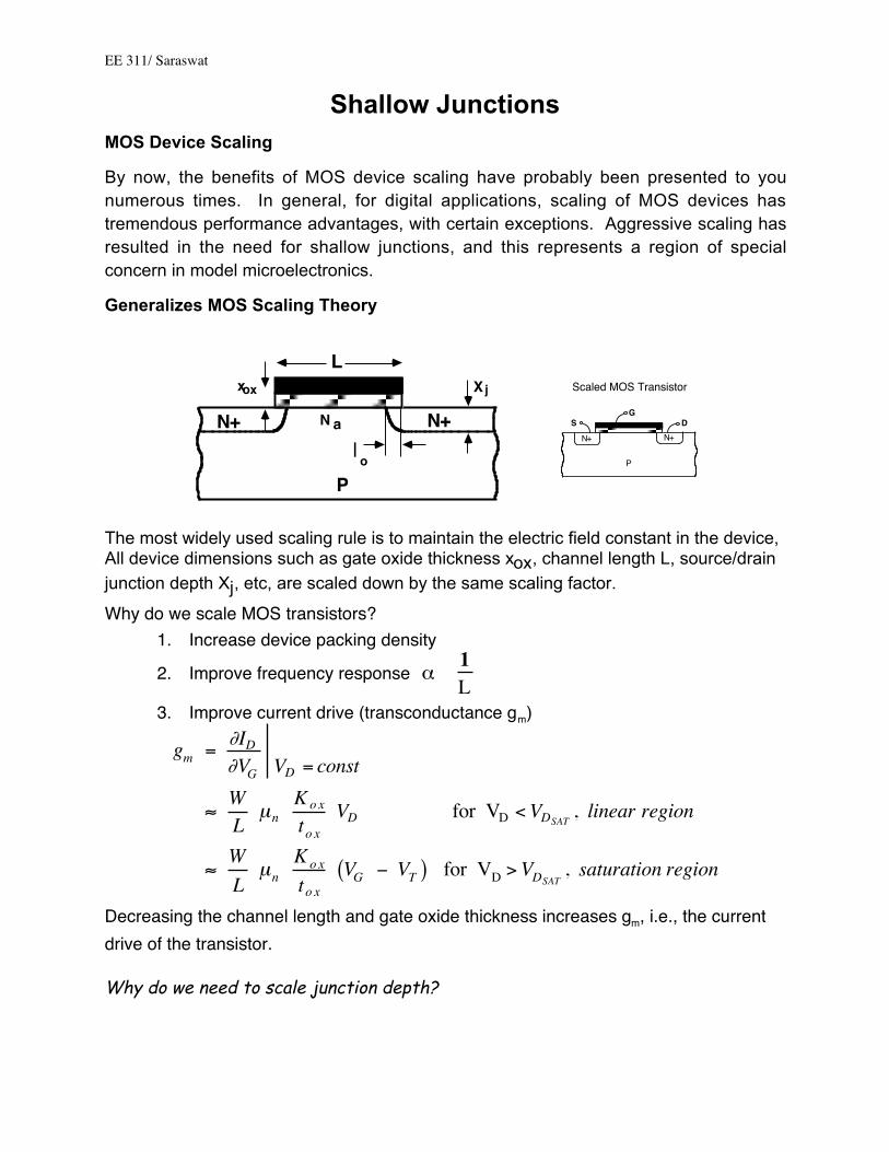
Shallow JunctionsMOS Device Scaling
By now, the benefits of MOS device scaling have probably been presented to younumerous times. In general, for digital applications, scaling of MOS devices hastremendous performance advantages, with certain exceptions. Aggressive scaling hasresulted in the need for shallow junctions, and this represents a region of specialconcern in model microelectronics.
Generalizes MOS Scaling Theory
N a
P
N+N+
Lxox Xj
ol P
N+N+S
GD
Scaled MOS Transistor
The most widely used scaling rule is to maintain the electric field constant in the device,All device dimensions such as gate oxide thickness xox, channel length L, source/drain
junction depth Xj, etc, are scaled down by the same scaling factor.
Why do we scale MOS transistors?1. Increase device packing density
2. Improve frequency response α1L
3. Improve current drive (transconductance gm)
€
gm =∂ID∂VG VD = const
≈WL
µnKo x
to xVD for VD <VDSAT
, linear region
≈WL
µnKo x
to xVG − VT( ) for VD >VDSAT
, saturation region
Decreasing the channel length and gate oxide thickness increases gm, i.e., the currentdrive of the transistor.
Why do we need to scale junction depth?
EE 311/ Saraswat Shallow Junctions
2
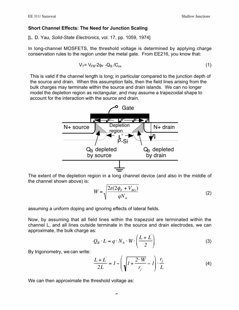
Short Channel Effects: The Need for Junction Scaling
[L. D. Yau, Solid-State Electronics, vol. 17, pp. 1059, 1974]
In long-channel MOSFETS, the threshold voltage is determined by applying chargeconservation rules to the region under the metal gate. From EE216, you know that:
VT= VFB-2φF -QB /Cox (1)
This is valid if the channel length is long; in particular compared to the junction depth ofthe source and drain. When this assumption fails, then the field lines arising from thebulk charges may terminate within the source and drain islands. We can no longermodel the depletion region as rectangular, and may assume a trapezoidal shape toaccount for the interaction with the source and drain.
Q depletedby source
Q depletedby drain
B B
N+ source N+ drain
Gate
P-Si
Depletion region
L’
L
rj
The extent of the depletion region in a long channel device (and also in the middle ofthe channel shown above) is:
€
W =2ε(2φF +VBG )
qNA (2)
assuming a uniform doping and ignoring effects of lateral fields.
Now, by assuming that all field lines within the trapezoid are terminated within thechannel L, and all lines outside terminate in the source and drain electrodes, we canapproximate, the bulk charge as:
QB ⋅ L = q ⋅ NA ⋅W ⋅L + L'
2
(3)
By trigonometry, we can write:
L + L'
2L= 1− 1+
2⋅Wrj
− 1
⋅rjL
(4)
We can then approximate the threshold voltage as:
EE 311/ Saraswat Shallow Junctions
3
VT = VFB − 2 ⋅φF −QB
Cox⋅ 1− 1 +
2 ⋅Wrj
−1
⋅rjL
(5)
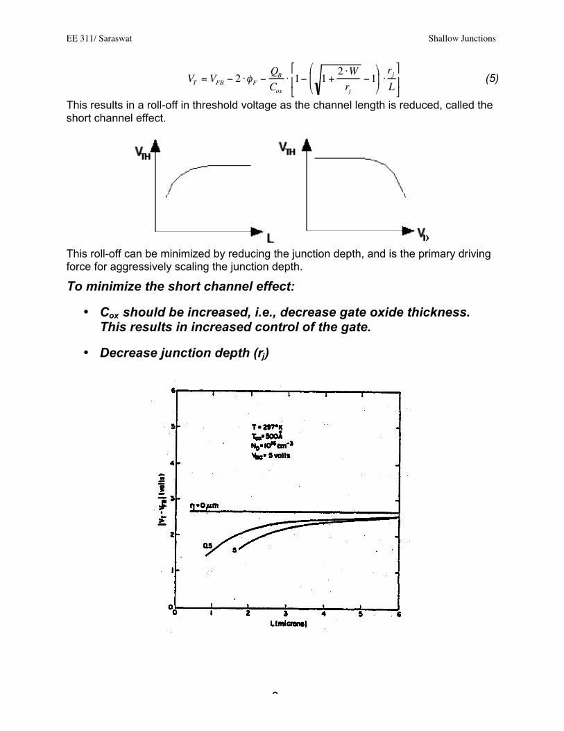
This results in a roll-off in threshold voltage as the channel length is reduced, called theshort channel effect.
This roll-off can be minimized by reducing the junction depth, and is the primary drivingforce for aggressively scaling the junction depth.
To minimize the short channel effect:
• Cox should be increased, i.e., decrease gate oxide thickness.This results in increased control of the gate.
• Decrease junction depth (rj)
EE 311/ Saraswat Shallow Junctions
4
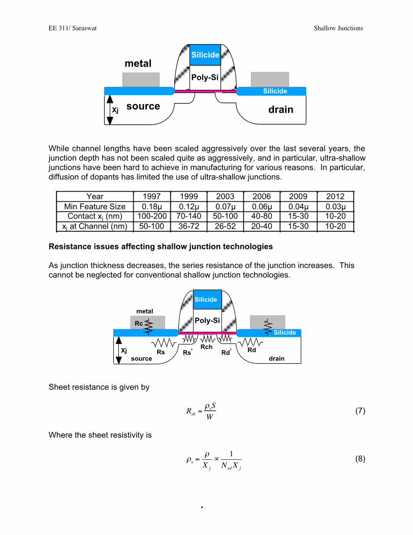
source
Silicide
drain
Silicide
metal
Xj
Poly-Si
While channel lengths have been scaled aggressively over the last several years, thejunction depth has not been scaled quite as aggressively, and in particular, ultra-shallowjunctions have been hard to achieve in manufacturing for various reasons. In particular,diffusion of dopants has limited the use of ultra-shallow junctions.
Year 1997 1999 2003 2006 2009 2012Min Feature Size 0.18µ 0.12µ 0.07µ 0.06µ 0.04µ 0.03µContact xj (nm) 100-200 70-140 50-100 40-80 15-30 10-20
xj at Channel (nm) 50-100 36-72 26-52 20-40 15-30 10-20
Resistance issues affecting shallow junction technologies
As junction thickness decreases, the series resistance of the junction increases. Thiscannot be neglected for conventional shallow junction technologies.
source
Rch
Silicide
Rc
Rsdrain
RdRd’Rs’
Silicide
metal
Xj
Poly-Si
Sheet resistance is given by
€
Rsh =ρsSW
(7)
Where the sheet resistivity is
€
ρs =ρX j
∝1
Nsd X j
(8)
EE 311/ Saraswat Shallow Junctions
5
The channel resistance can be approximated by
)( thgs
oxchch VV
tLR
−∝
(9)
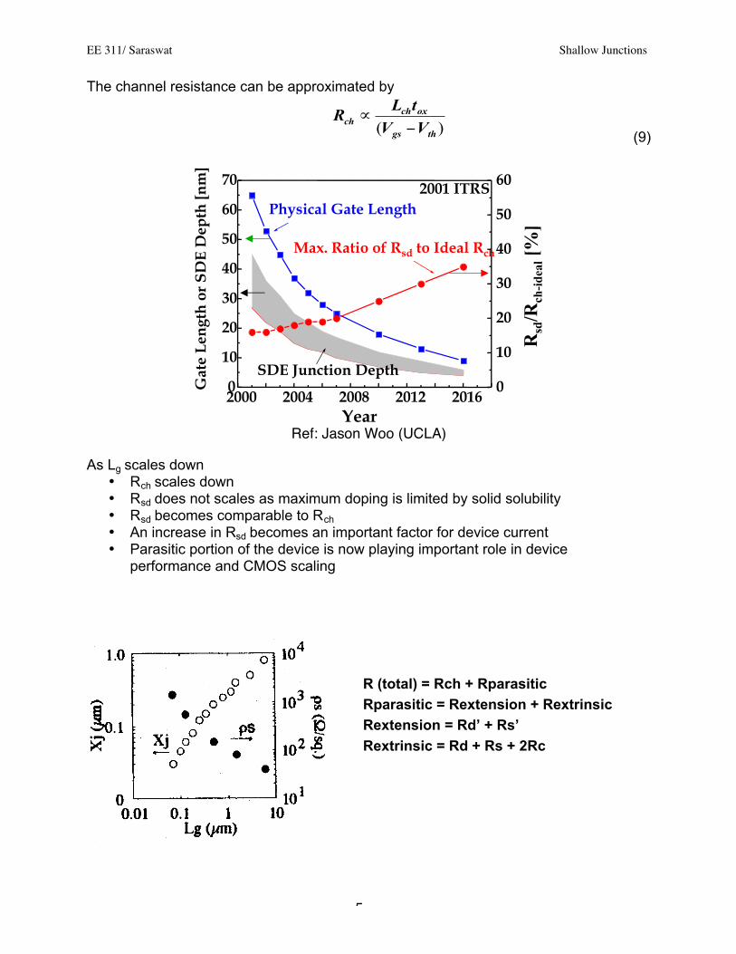
2000 2004 2008 2012 20160
10
20
30
40
50
60
70
SDE Junction Depth
Max. Ratio of Rsd to Ideal Rch
Physical Gate Length2001 ITRS
Gat
e L
engt
h o
r S
DE
Dep
th [n
m]
Year
0
10
20
30
40
50
60
Rsd
/Rch
-ide
al [
%]
Ref: Jason Woo (UCLA)
As Lg scales down• Rch scales down• Rsd does not scales as maximum doping is limited by solid solubility• Rsd becomes comparable to Rch
• An increase in Rsd becomes an important factor for device current• Parasitic portion of the device is now playing important role in device
performance and CMOS scaling
R (total) = Rch + Rparasitic
Rparasitic = Rextension + Rextrinsic
Rextension = Rd’ + Rs’
Rextrinsic = Rd + Rs + 2Rc

EE 311/ Saraswat Shallow Junctions
6
Various parasitic source/drain resistance components compared to the channelresistance. With scaling of channel length the parasitic resistance becomes comparableto channel resistance. (After Ohguro, et al., ULSI Science and Technology 1997,Electrochemical Soc. Proc., Vol. 97-3)
How are we going to fabricate such shallow junctions?
Dopant Diffusion
Gate Stack
Anneal/Diffusion
Ion Implant
You have already studied dopant diffusion in EE212. Equations of diffusion are typicallyderived from Fick's laws. Solutions to diffusion equations typically involve a diffusivityparameter:
Di = Dio ⋅ e
_EO k⋅T (10)
Diffusion is an important issue in shallow junction device technology since it places alower limit on the ability to fabricate shallow junctions. After doping, thermal processesare used for dopant activation, silicidation, and dielectric reflow steps in conventionalMOS processes. These result in some dopant redistribution. Hence, an understandingof diffusion processes, particularly as they apply to conventional shallow junctiontechnology, is extremely important.
The bulk diffusivity values for various dopants have been studied in great detail. Inshallow junction technologies, numerous effects alter these values, typically resulting inenhanced diffusion.

EE 311/ Saraswat Shallow Junctions
7
1. Transient enhanced diffusion - For short times during the initial stages of a thermalcycle, diffusion is enhanced over traditional diffusivity values. This is called transientenhanced diffusion. In particular, defects tend to increase this effect substantially.This has an important implication in shallow junctions, since diffusion is enhancedinitially, when the junction region is full of defects caused by ion implantation.
D = Di + Do ⋅ e_ tτ
An important technological change that has resulted from this is the increased use ofrapid thermal annealing for dopant activation. Even though higher temperaturesmay be used to activate the dopants, diffusion is less than with longer, lowertemperature furnace anneals of equivalent thermal budget.
2. Enhanced diffusion through defects - As mentioned above, diffusion is enhancedthrough the presence of various defects. Thermal oxidation can change theconcentration of interstitials and vacancies.
TSUPREM IV simulations of oxidation enhanced diffusion of boron (OED) and oxidationretarded diffusion of antimony (ORD) during the growth of a thermal oxide on thesurface of silicon. The two shallow profiles are antimony, the two deeper profiles areboron. Oxidation increases CI and decreases CV from their equilibrium values. (Ref:Plummer, et al., Silicon VLSI Technology - Fundamentals, Practice and Models)
The worst-case demonstration of the defect enhanced diffusion of dopants is inpolycrystalline silicon, which can be several times faster than diffusion in bulk Sibecause of defects at the grain boundaries..

EE 311/ Saraswat Shallow Junctions
8
Similarly, end of range defects resulting from ion-implantation tend to enhancediffusion of dopants. This is therefore important in shallow junctions, since these aretypically formed through heavy ion implantation in conventional processes. At lowertemperatures, the damage can stay around longer and enhance the dopant diffusion,while at higher temperatures the damage annihilates faster. Thus the diffusivity is afunction of time during the transient.
TSUPREM IV simulation of the time evolution of the damage from a 40keV, 10-14 cm-2 boron implant, for anneals from 10-6 sec to 10-1 sec at750˚C. The equilibrium interstitial concentration is approximately 108 cm-3,so the flat concentration profile at 10-1 sec represents an interstitialsupersaturation of more than 10,000 fold, and TED occurs until surfacerecombination reduces this to equilibrium levels. (Ref: Plummer, et al.,Silicon VLSI Technology - Fundamentals, Practice and Models)
DGB grain boundary diffusionDL lattice diffusionGenerally DGB >> DL

EE 311/ Saraswat Shallow Junctions
9
Duration of TED plotted versus temperature from a 40 keV, 10-14 cm-2
boron implant.
Temperature dependence of transient enhanced diffusion, showing morediffusion for lower temperatures. (After Plummer, et al.)
• At lower temperature longer times are needed to anneal the damage
• Transient enhanced dopant diffusion effects are stronger
• Junction depth is larger
• Higher temperature and shorter times are needed to minimize TED
Shallow junction formation technologies
Low Energy Implantation
Conventional shallow junctions are made using low energy implants followed by rapidthermal annealing to activate the dopants. This works well for n+ junctions, which are

EE 311/ Saraswat Shallow Junctions
10
formed using As' As is a large atom, and therefore has a lower implantation range for agiven energy than smaller atoms such as P and B. Additionally, channeling is not assevere a problem, and it is therefore possible to obtain box-like profiles for As-dopedsource / drain junctions. Implantation is typically performed at a 7' angle to minimizechanneling.
Profiles of 40 keV As and B implants Profiles of 12 keV BF2 and B implants
BF2 has been used as a p-type implantation species, since it is heavier and has a lowerprojection depth. However, F appears to retard defect annealing, and may thereforeenhance TED.
0 20 40 60 801016
1018
1020
1022
Depth (nm)
As (cm-3) 5 keV
1 keV
as-implanted
As
Co
nce
ntr
atio
n (
cm-3
)
Profiles of 1 and 5 keV As implant measured by two differenttechniques. (Ref. Kasnavi, PhD Thesis, Stanford Univ. 2001)
From the above plots, two important characteristics that limit scaling are apparent:
1. Peak depth - In general, to achieve shallow p+ junctions, extremely low energiesare required. Typical implanters do not work well below 5keV. Extraction current isextremely low in these ranges, and implants may take hours due to the low ioncurrent. In recent years, advances in implanter technology have resulted in thedemonstration of implants as low as 5OOeV (Hong et al, IEEE Trans. ElectronDev., vol. 3 8, pp. 28, 199 1).
2. Channeling - In EE212, you were introduced to channeling during implantation.This is a particularly important problem for shallow junctions, since channeling candominate the final junction depth and use of tilted implants does not solve theproblem at low energies.

EE 311/ Saraswat Shallow Junctions
11
Ion Implantation Damage
Light ions (B), lower energy Heavy ions (As, P), higher energy
Buried damage
regrowth
fully annealed
⇓⇓
After implant
After anneal
• Heavy ions (As, P), higher energy cause excessive damage throughoutthe implanted region as the energy loss is due to nuclear stopping. If thedose is heavy the damage turns the implanted region into amorphous.
• Light ions (B), lower energy have buried damage as the energy loss isdue to electronic stopping.
• Fully amorphized region can be fully annealed through solid phaseregrowth
• Buried damage leaves defects where damage was created as regrowthtakes place both from top and bottom.

EE 311/ Saraswat Shallow Junctions
12
Pre-amorphization implants
[Wilson, J. Appl. Phys., vol. 54, pp. 6879, 1983Hong et al, IEEE Trans. Electron. Dev., vol. 38, pp. 28, 1991Osburn, et al, J. Electrochem. Soc., vol. 139, pp. 2291, August 1992]
A solution to channeling is to use pre-amorphization implants prior to dopantimplantation. Within the amorphized region, there is no channeling, by definition.
Boron depth profiles obtained with 10 keV, 5x10¹⁴ BF2/cm2 implants withno preamorphization and with Ge (40 keV, 5x10¹⁴) or Si (30 keV, 5x10¹⁴)preamorphization before or after a 10 sec. 1000°C RTA
Initially, Si implants were used to achieve amorphization. However, a high dose isrequired since Si is a relatively small atom. Much lower pre-amorphization doses canbe achieved using Ge instead. Note that both of these result in the formation of end-of-range defects near the amorphized interface, which enhance TED, and can also act asgeneration-recombination centers if they are not annealed out and lie within thedepletion region. This results in increased junction leakage, and therefore, care mustbe taken in the placement of the amorphization peak. The enhance TED in generalresults in junction depth similar with and without preamorphization.

EE 311/ Saraswat Shallow Junctions
13
Solid Source Diffusion
[Jiang et al, J. Electrochem. Soc., vol. 139, pp. 211, 1992]
One of the problems with implantation is that it introduces defects into the implantedregion. These require subsequent annealing, and during this period, diffusion isenhanced. An alternative technology is the use of solid-source diffusion. In thisprocess, a doped highly diffusing region located in contact with the junction area is usedto diffuse dopants into the Si. Since there is no implantation damage, it is possible toform shallow junctions. Silicides are common diffusing layers due to their high dopantdiffusivity.
Shallow junction formation by diffusion from a doped silicide
Fig. SIMS boron profiles after diffusion at 950°C of 50 nm COSi2 implantedwith 5 X 1015 cm-2 BF2 (a) in COSi2 and (b)in Si after silicide removal.
EE 311/ Saraswat Shallow Junctions
14
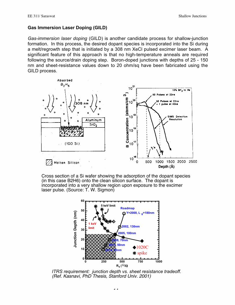
Gas Immersion Laser Doping (GILD)
Gas-immersion laser doping (GILD) is another candidate process for shallow-junctionformation. In this process, the desired dopant species is incorporated into the Si duringa melt/regrowth step that is initiated by a 308 nm XeCl pulsed excimer laser beam. Asignificant feature of this approach is that no high-temperature anneals are requiredfollowing the source/drain doping step. Boron-doped junctions with depths of 25 - 150nm and sheet-resistance values down to 20 ohm/sq have been fabricated using theGILD process.
Cross section of a Si wafer showing the adsorption of the dopant species(in this case B2H6) onto the clean silicon surface. The dopant isincorporated into a very shallow region upon exposure to the excimerlaser pulse. (Source: T. W. Sigmon)
0 250 500 750 10000
10
20
30
40
50
60
Xj (nm)
Rs (Ω/ )
Y=2000, L g=180nm
2002, 130nm
Roadmap
2011, 50nm
2014, 35nm
2008, 70nm
2005, 100nm
1 keVlimit
5 keV limit
1020Cspike
Jun
ctio
n D
epth
(n
m)
ITRS requirement: junction depth vs. sheet resistance tradeoff.(Ref. Kasnavi, PhD Thesis, Stanford Univ. 2001)

EE 311/ Saraswat Shallow Junctions
15
Solutions to Shallow Junction Resistance Problem
Extension implants
One way around the shallow junction resistance problem is to use a shallowjunction close to the channel, but a deeper junction further away. Thus, VT roll-off is suppressed without increased parasitic resistances too much. Theextension implant may be performed through a spacer oxide, or by using anultra-low energy implant.
While this solution helps, it does not completely solve the problem, since the thindoped silicon still has a resistance that is rather high for use on a deep-submicron device.
Elevated source/ drain devices
One solution is to use a substantially thicker source drain by using an elevationscheme to increase the thickness. Using selective epitaxy, it is possible toimplement such a scheme within the confines of a conventional MOSFETprocess.
By using this technique, it is possible to lower the source/drain resistance of theMOSFET. Additionally, the raised region can be consumed to form a low-resistancesilicide, as shall be shown later. It can also be used as a diffusion source to form ashallow junction.

EE 311/ Saraswat Shallow Junctions
16
Silicon selective epitaxy is achieved through the use of chemistries than havecompeting etching and deposition reactions. The most common chemistry used indichlorosilane (SiH2CL2) and HCL.
SiH2Cl2 → SiCl2 + H2
SiCl2 + H2 → Si + 4 ⋅HCl
The byproduct HCI, along with any HCI added to the system in the gas-phase, can etchSi as well.
Si + 2 ⋅ HCl→ SiCl2 + H2
Now, selectivity is achieved by taking advantage of the fact that initial growth of siliconis faster on a silicon substrate than on an oxide (or nitride) substrate. Therefore, byoptimizing the HCI ratio, it is possible to ensure than any nuclei forming on the oxide areetched away, while the silicon continues to grow (albeit at a reduced rate).
One of the important requirements for selective epitaxy is that there is no native oxideover the silicon (otherwise, deposition, by definition, would be impossible). Therefore,epitaxy is usually preceded by a hydrogen bake to remove the native oxide. Hydrogenis a mild etchant of SiO2, SO the native oxide is removed without consuming too much ofthe oxide in the field regions.
Thus, the conditions have been established to perform selective epitaxy.
Salicidation
The dominant technology for forming low resistance shallow junctions is salicidation. In thisprocess, a low resistance silicide is formed over the source / drain diffusions. Thus, the sheetresistance is reduced, and the contact area is increased as well, since the process is self-aligned.

EE 311/ Saraswat Shallow Junctions
17
Various parasitic source/drain resistance components with and without silicidation. (Ref:Ohguro, et al., ULSI Science and Technology 1997, Electrochemical Soc. Proc., Vol. 97-3)
Salicidation has become a very important process in the fabrication of high performance logicdevices. In fact, the driving force for selective epitaxy research is salicidation itself, since somesilicon is consumed in this process, and selective epitaxy allows greater process margins.
Elevated S/D structure ⇒ Reduction of Rcsd by increasing Nif & reducing Rsh,dp
underneath silicide
=
T
con
T
ccsd L
L
LR coth
ρ
dpsh
c
RLT
,
ρ=
∝
if
bc
N
qφρ exp

EE 311/ Saraswat Shallow Junctions
18
Ref: A. Hokazono et al (Toshiba), IEDM2000
Schottky Barrier Source/Drain SOI MOSFET
One way to minimize parasitic resistance is to replace the diffused junctions bySchottky barrier source/drain. Since Schottky barriers are made of highly conductivemetals or silicides, the resistance caused by diffused junctions is eliminated. However,unlike the p-n junction barrier the Schottky barrier can’t be modulated by the gate. Thismay reduce the drive current of the MOSFET. This technology may become importantfor nanometer scale devices.
BOX
Si
Schottky Barrier
Silicid

EE 311/ Saraswat Shallow Junctions
19
Effect of Extrinsic Resistance on Double Gate MOSFETs
It is widely accepted that alternative (non-classical) MOSFET structures will be neededfor prolonging device scaling at the end of the ITRS Roadmap. The ultrathin body double-gate FET (DGFET) is one of the leading candidates for replacing conventional bulkCMOS transistors. The DGFET has been shown to have very good electrostatic gatecontrol over the channel, enabling gate length scaling down to 10nm. Experimentalprototypes of DGFETs have been demonstrated in both planar as well as fin-likegeometries (FinFET). In these devices, the ultrathin body, whose thickness is typically 1/3to 1/2 of the gate length, is key to suppressing short channel effects, such as Vt rolloff,DIBL, and degraded subthreshold swing. However, it also introduces an extrinsicparasitic resistance Rs in series with the channel and the source/drain electrodes. Theeffective gate overdrive is reduced by an amount Id⋅Rs, where Id is the drain-sourcecurrent when the transistor is turned on and in saturation. As a result, thetransconductance and performance, as measured by drive current Ion and intrinsicswitching delay (CV/I), is degraded even though the intrinsic device has nearly ballisticcarrier transport. This problem is even more severe in a DGFET since the presence oftwo channels implies that twice the current flows through the series resistance, leading tohigher potential drop across the extrinsic resistance.
Fig. Schematic cross section of the double gate MOSFET structure and
1.E+13
1.E+14
1.E+15
1.E+16
1.E+17
1.E+18
1.E+19
1.E+20
1.E+21
40 45 50 55 60 65
x (nm)
Net
Dop
ing
(cm
-3)
5nm/dec
4nm/dec3nm/dec
2nm/dec1nm/dec
0.5nm/dec
GATE
Lateral doping profile in the source extension region for 3 values of lateral dopinggradient (LDG) (bottom)
EE 311/ Saraswat Shallow Junctions
20
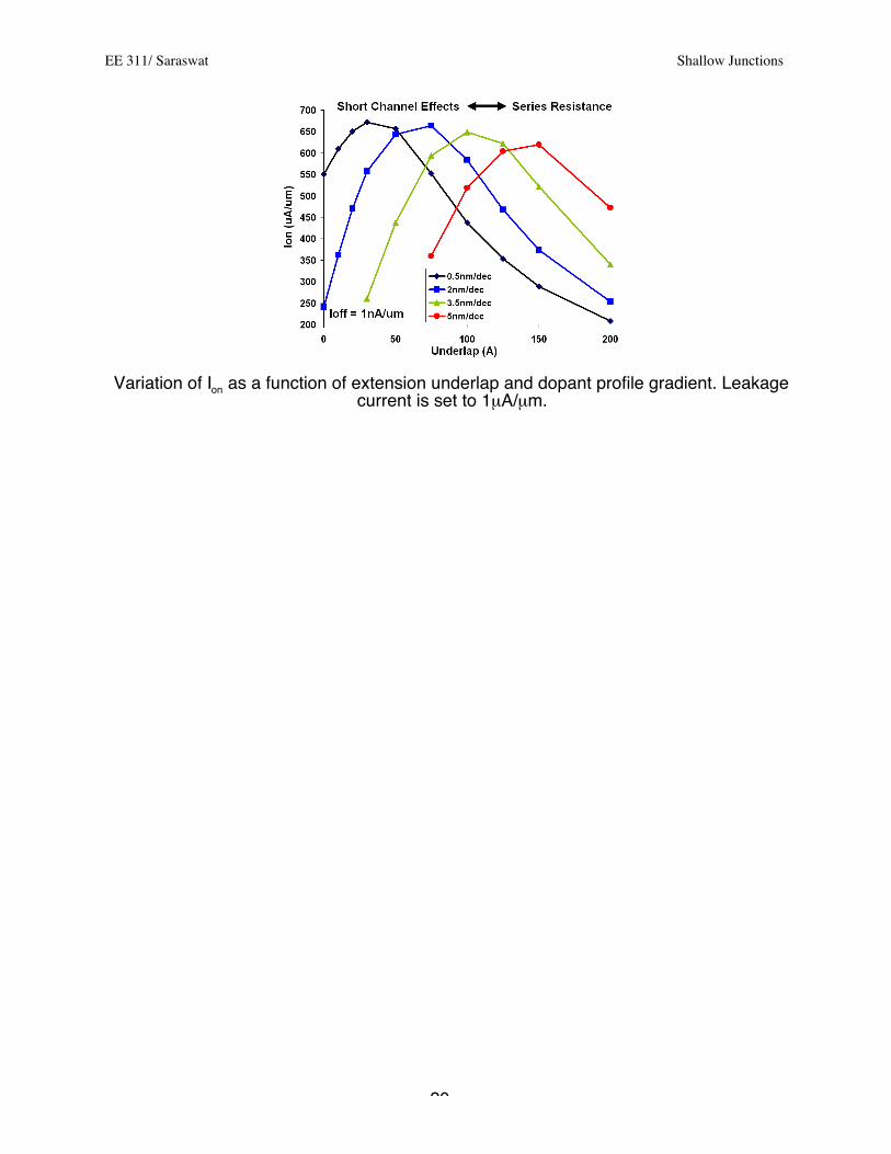
Variation of Ion as a function of extension underlap and dopant profile gradient. Leakagecurrent is set to 1µA/µm.