eecs130 integrated circuit devicesee130/fa07/lectures/ms... · 2007-10-02 · eecs130 integrated...
TRANSCRIPT

EECS130 Integrated Circuit Devices
Professor Ali Javey10/02/2007
MS Junctions, Lecture 2MOS Cap, Lecture 1
Reading: finish chapter14, start chapter16

Announcements
• Professor Javey will hold his OH at 3-5 pm for Wednesday (400 Cory).
• Exam review: 8-10 pm tonight, (521 Cory).
• Exam: Thursday. Make sure you come early .

Carrier Injection at the MS Contacts
– Thermionic emission current
– Tunneling current
– Thermally activated tunneling current
For each MS junction, 3 components contribute to the overall injection current:
What parameters affect each component?

Is the net current zero? Why?


Question:
How do p+n junctions differ from MS junctions under a forward bias?

Question
• How does the band diagram look for a MS junction with a Schottky barrier height of zero?


Applications of Schottky Diodes
• I0 of a Schottky diode is 103 to 108 times larger than a PN junction diode, depending on φB . • A Schottky diode is the preferred rectifier in low voltage, high current applications.
I
V
PN junction
Schottky
φB
I
V
PN junction
Schottky diode
φBdiode

Ohmic MS Contacts
Two ways to achieve ohmic MS contacts:– Reduce the Schottky barrier height. How???– Reduce the Schottky barrier width (depletion
width). How????
How would each approach give you an ohmic contact?


Schottky Barriers and Fermi Level Pinning
In actual fabricated metal-Si junctions, Fermi level pinning prevents us from ever getting zero Schottky barrier height.
Two tricks for reducing Fermi level pinning: 1. thin interfacial oxide/nitride2. 1D semiconductors
1D nanotubeDiameter ~ 1 nm

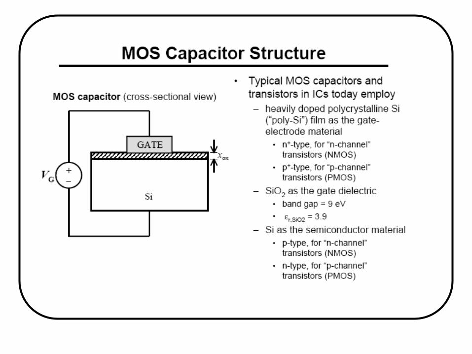
MOS Capacitors (MOSC)
MOS: Metal-Oxide-Semiconductor
SiO2
metal
gate
Si body
Vg
gate
Si-body (P)
N+
MOS capacitor
MOS transistor
Vg
SiO2
N+
Chapter 16
MOS transistor is the most important device in modern microelectronics.

Ideal MOS Capacitor– Oxide has zero charge, and no current can pass through it.– No charge centers are present in the oxide or at the oxide-
semiconductor interface.– Semiconductor is uniformly doped– ΦM = ΦS = χ
+ (EC – EF )FB

Ideal MOS Capacitor At Equilibrium:

Ideal MOS Capacitor Under Bias
– Let us ground the semiconductor and start applying different voltages, VG , to the gate
– VG can be positive, negative or zero with respect to the semiconductor
– EF,metal – EF,semiconductor = – q VG
– Since oxide has no charge (it’s an insulator with no available carriers or dopants), d Eoxide / dx = ρ/ε
= 0; meaning that the E-field inside the oxide is constant.

P-type Si, VG < 0 (accumulation)ε
EC
Ei
EVEFs
GqV
mΦ Accumulationof holes
xqx ∂∂
==⇒=∂
∂ ioxide
oxide 1const.0 EE
E
•The oxide energy band has constant slope as shown. •No current flows in the SiO2 layer EF in Si is constant.
Negative voltage attracts holes to the Si-oxide interface.This is called accumulation condition.Ei – EF
shouldincreases near thesurface of Si.

P-type Si, VG < 0 (accumulation)
–
–
–
–
+
+
Sheet of holes
ρE
M O SVG < 0
Sheet ofelectrons
xAccumulation of holes nearsilicon surface, and electronsnear the metal surface.
Similar to a parallel platecapacitor structure.

p-type Si, VG > 0 (depletion)
EFM
ECEiEFsEV
DepletionE
OM S
positive=ρ
0=ρnegative=ρ
+
+
+- - - -
- - - -
E

p-type Si, VG >> 0 (inversion)
EC
Ei
EV
EFM
+
+
+
+
- - - - - - -
- - - - - - --
-
Immobile acceptors
Mobile electrons
EFM
EFS
E

Inversion conditionIf we continue to increase the positive gate voltage, the bands at the semiconductor bends more strongly. At sufficiently high voltage, Ei
can be below EF
indicating large concentration of electrons in the conduction band.
We say the material near the surface is “inverted”. The “inverted”
layer is not gotten by chemical doping, but by
applying E-field. Where did we get the electrons from?
When Ei
(surface) –
Ei
(bulk) = 2 [EF
– Ei
(bulk)], the condition is start of “inversion”, and the voltage VG
applied to gate is called VT
(threshold voltage).
For VG > VT
, the Si surface is inverted.

Ideal MOS Capacitor – n-type Si

In what direction do the electrons flow in order to reach equilibrium?What path do they take to reach equilibrium?
The Case of ΦM
≠ ΦS