sh7670 group user's manual: hardware
TRANSCRIPT

User's M
anual
All information contained in these materials, including products and product specifications, represents information on the product at the time of publication and is subject to change by Renesas Electronics Corp. without notice. Please review the latest information published by Renesas Electronics Corp. through various means, including the Renesas Electronics Corp. website (http://www.renesas.com).
SH7670 Group
User’s Manual: Hardware32
Rev.3.00 Jun 2011
Renesas 32-Bit RISC Microcomputer SuperHTM RISC engine Family / SH7670 Series
SH7670 R5S76700SH7671 R5S76710SH7672 R5S76720SH7673 R5S76730
www.renesas.com
The revision list summarizes the locations of revisions and additions. Details should always be checked by referring to the relevant text.

Page ii of xxvi
Page iii of xxvi
Notice1. All information included in this document is current as of the date this document is issued. Such information, however, is
subject to change without any prior notice. Before purchasing or using any Renesas Electronics products listed herein, please
confirm the latest product information with a Renesas Electronics sales office. Also, please pay regular and careful attention to
additional and different information to be disclosed by Renesas Electronics such as that disclosed through our website.
2. Renesas Electronics does not assume any liability for infringement of patents, copyrights, or other intellectual property rights
of third parties by or arising from the use of Renesas Electronics products or technical information described in this document.
No license, express, implied or otherwise, is granted hereby under any patents, copyrights or other intellectual property rights
of Renesas Electronics or others.
3. You should not alter, modify, copy, or otherwise misappropriate any Renesas Electronics product, whether in whole or in part.
4. Descriptions of circuits, software and other related information in this document are provided only to illustrate the operation of
semiconductor products and application examples. You are fully responsible for the incorporation of these circuits, software,
and information in the design of your equipment. Renesas Electronics assumes no responsibility for any losses incurred by
you or third parties arising from the use of these circuits, software, or information.
5. When exporting the products or technology described in this document, you should comply with the applicable export control
laws and regulations and follow the procedures required by such laws and regulations. You should not use Renesas
Electronics products or the technology described in this document for any purpose relating to military applications or use by
the military, including but not limited to the development of weapons of mass destruction. Renesas Electronics products and
technology may not be used for or incorporated into any products or systems whose manufacture, use, or sale is prohibited
under any applicable domestic or foreign laws or regulations.
6. Renesas Electronics has used reasonable care in preparing the information included in this document, but Renesas Electronics
does not warrant that such information is error free. Renesas Electronics assumes no liability whatsoever for any damages
incurred by you resulting from errors in or omissions from the information included herein.
7. Renesas Electronics products are classified according to the following three quality grades: "Standard", "High Quality", and
"Specific". The recommended applications for each Renesas Electronics product depends on the product's quality grade, as
indicated below. You must check the quality grade of each Renesas Electronics product before using it in a particular
application. You may not use any Renesas Electronics product for any application categorized as "Specific" without the prior
written consent of Renesas Electronics. Further, you may not use any Renesas Electronics product for any application for
which it is not intended without the prior written consent of Renesas Electronics. Renesas Electronics shall not be in any way
liable for any damages or losses incurred by you or third parties arising from the use of any Renesas Electronics product for an
application categorized as "Specific" or for which the product is not intended where you have failed to obtain the prior written
consent of Renesas Electronics. The quality grade of each Renesas Electronics product is "Standard" unless otherwise
expressly specified in a Renesas Electronics data sheets or data books, etc.
"Standard": Computers; office equipment; communications equipment; test and measurement equipment; audio and visual
equipment; home electronic appliances; machine tools; personal electronic equipment; and industrial robots.
"High Quality": Transportation equipment (automobiles, trains, ships, etc.); traffic control systems; anti-disaster systems; anti-
crime systems; safety equipment; and medical equipment not specifically designed for life support.
"Specific": Aircraft; aerospace equipment; submersible repeaters; nuclear reactor control systems; medical equipment or
systems for life support (e.g. artificial life support devices or systems), surgical implantations, or healthcare
intervention (e.g. excision, etc.), and any other applications or purposes that pose a direct threat to human life.
8. You should use the Renesas Electronics products described in this document within the range specified by Renesas Electronics,
especially with respect to the maximum rating, operating supply voltage range, movement power voltage range, heat radiation
characteristics, installation and other product characteristics. Renesas Electronics shall have no liability for malfunctions or
damages arising out of the use of Renesas Electronics products beyond such specified ranges.
9. Although Renesas Electronics endeavors to improve the quality and reliability of its products, semiconductor products have
specific characteristics such as the occurrence of failure at a certain rate and malfunctions under certain use conditions. Further,
Renesas Electronics products are not subject to radiation resistance design. Please be sure to implement safety measures to
guard them against the possibility of physical injury, and injury or damage caused by fire in the event of the failure of a
Renesas Electronics product, such as safety design for hardware and software including but not limited to redundancy, fire
control and malfunction prevention, appropriate treatment for aging degradation or any other appropriate measures. Because
the evaluation of microcomputer software alone is very difficult, please evaluate the safety of the final products or system
manufactured by you.
10. Please contact a Renesas Electronics sales office for details as to environmental matters such as the environmental
compatibility of each Renesas Electronics product. Please use Renesas Electronics products in compliance with all applicable
laws and regulations that regulate the inclusion or use of controlled substances, including without limitation, the EU RoHS
Directive. Renesas Electronics assumes no liability for damages or losses occurring as a result of your noncompliance with
applicable laws and regulations.
11. This document may not be reproduced or duplicated, in any form, in whole or in part, without prior written consent of Renesas
Electronics.
12. Please contact a Renesas Electronics sales office if you have any questions regarding the information contained in this
document or Renesas Electronics products, or if you have any other inquiries.
(Note 1) "Renesas Electronics" as used in this document means Renesas Electronics Corporation and also includes its majority-
owned subsidiaries.
(Note 2) "Renesas Electronics product(s)" means any product developed or manufactured by or for Renesas Electronics.

Page iv of xxvi
General Precautions in the Handling of MPU/MCU Products
The following usage notes are applicable to all MPU/MCU products from Renesas. For detailed usage notes on the products covered by this manual, refer to the relevant sections of the manual. If the descriptions under General Precautions in the Handling of MPU/MCU Products and in the body of the manual differ from each other, the description in the body of the manual takes precedence.
1. Handling of Unused Pins Handle unused pins in accord with the directions given under Handling of Unused Pins in the manual. ⎯ The input pins of CMOS products are generally in the high-impedance state. In operation
with an unused pin in the open-circuit state, extra electromagnetic noise is induced in the vicinity of LSI, an associated shoot-through current flows internally, and malfunctions occur due to the false recognition of the pin state as an input signal become possible. Unused pins should be handled as described under Handling of Unused Pins in the manual.
2. Processing at Power-on The state of the product is undefined at the moment when power is supplied. ⎯ The states of internal circuits in the LSI are indeterminate and the states of register
settings and pins are undefined at the moment when power is supplied. In a finished product where the reset signal is applied to the external reset pin, the states of pins are not guaranteed from the moment when power is supplied until the reset process is completed. In a similar way, the states of pins in a product that is reset by an on-chip power-on reset function are not guaranteed from the moment when power is supplied until the power reaches the level at which resetting has been specified.
3. Prohibition of Access to Reserved Addresses Access to reserved addresses is prohibited. ⎯ The reserved addresses are provided for the possible future expansion of functions. Do
not access these addresses; the correct operation of LSI is not guaranteed if they are accessed.
4. Clock Signals After applying a reset, only release the reset line after the operating clock signal has become stable. When switching the clock signal during program execution, wait until the target clock signal has stabilized. ⎯ When the clock signal is generated with an external resonator (or from an external
oscillator) during a reset, ensure that the reset line is only released after full stabilization of the clock signal. Moreover, when switching to a clock signal produced with an external resonator (or by an external oscillator) while program execution is in progress, wait until the target clock signal is stable.
5. Differences between Products Before changing from one product to another, i.e. to one with a different type number, confirm that the change will not lead to problems. ⎯ The characteristics of MPU/MCU in the same group but having different type numbers may
differ because of the differences in internal memory capacity and layout pattern. When changing to products of different type numbers, implement a system-evaluation test for each of the products.

Page v of xxvi
How to Use This Manual
1. Objective and Target Users
This manual was written to explain the hardware functions and electrical characteristics of this LSI to the target users, i.e. those who will be using this LSI in the design of application systems. Target users are expected to understand the fundamentals of electrical circuits, logic circuits, and microcomputers.
This manual is organized in the following items: an overview of the product, descriptions of the CPU, system control functions, and peripheral functions, electrical characteristics of the device, and usage notes.
When designing an application system that includes this LSI, take all points to note into account. Points to note are given in their contexts and at the final part of each section, and in the section giving usage notes.
The list of revisions is a summary of major points of revision or addition for earlier versions. It does not cover all revised items. For details on the revised points, see the actual locations in the manual.
The following documents have been prepared for the SH7670 Group. Before using any of the documents, please visit our web site to verify that you have the most up-to-date available version of the document.
Document Type Contents Document Title Document No.
Data Sheet Overview of hardware and electrical characteristics
⎯ ⎯
User's manual for Hardware
Hardware specifications (pin assignments, memory maps, peripheral specifications, electrical characteristics, and timing charts) and descriptions of operation
SH7670 Group User's Manual: Hardware
This User's manual
User's manual for Software
Detailed descriptions of the CPU and instruction set
SH-2A, SH2A-FPU Software Manual
REJ09B0051
Application Note Examples of applications and sample programs
Renesas Technical Update
Preliminary report on the specifications of a product, document, etc.
The latest versions are available from our web site.

Page vi of xxvi
2. Description of Numbers and Symbols
Aspects of the notations for register names, bit names, numbers, and symbolic names in this manual are explained below.
CMCSR indicates compare match generation, enables or disables interrupts, and selects the counter input clock. Generation of a WDTOVF signal or interrupt initializes the TCNT value to 0.
14.3 Operation
The style "register name"_"instance number" is used in cases where there is more than one instance of the same function or similar functions.[Example] CMCSR_0: Indicates the CMCSR register for the compare-match timer of channel 0.
In descriptions involving the names of bits and bit fields within this manual, the modules and registers to which the bits belong may be clarified by giving the names in the forms "module name"."register name"."bit name" or "register name"."bit name".
(1) Overall notation
(2) Register notation
Rev. 0.50, 10/04, page 416 of 914
14.2.2 Compare Match Control/Status Register_0, _1 (CMCSR_0, CMCSR_1)
14.3.1 Interval Count Operation
(4)
(3)
(2)
Binary numbers are given as B'nnnn (B' may be omitted if the number is obviously binary), hexadecimal numbers are given as H'nnnn or 0xnnnn, and decimal numbers are given as nnnn.[Examples] Binary: B'11 or 11 Hexadecimal: H'EFA0 or 0xEFA0 Decimal: 1234
(3) Number notation
An overbar on the name indicates that a signal or pin is active-low.[Example] WDTOVF
Note: The bit names and sentences in the above figure are examples and have nothing to dowith the contents of this manual.
(4) Notation for active-low
When an internal clock is selected with the CKS1 and CKS0 bits in CMCSR and the STR bit in CMSTR is set to 1, CMCNT starts incrementing using the selected clock. When the values in CMCNT and the compare match constant register (CMCOR) match, CMCNT is cleared to H'0000 and the CMF flag in CMCSR is set to 1. When the CKS1 and CKS0 bits are set to B'01 at this time, a f/4 clock is selected.

Page vii of xxvi
3. Description of Registers
Each register description includes a bit chart, illustrating the arrangement of bits, and a table of bits, describing the meanings of the bit settings. The standard format and notation for bit charts and tables are described below.
Indicates the bit number or numbers.In the case of a 32-bit register, the bits are arranged in order from 31 to 0. In the caseof a 16-bit register, the bits are arranged in order from 15 to 0.
Indicates the name of the bit or bit field.When the number of bits has to be clearly indicated in the field, appropriate notation is included (e.g., ASID[3:0]).A reserved bit is indicated by "−".Certain kinds of bits, such as those of timer counters, are not assigned bit names. In such cases, the entry under Bit Name is blank.
(1) Bit
(2) Bit name
Indicates the value of each bit immediately after a power-on reset, i.e., the initial value.0: The initial value is 01: The initial value is 1−: The initial value is undefined
(3) Initial value
For each bit and bit field, this entry indicates whether the bit or field is readable or writable, or both writing to and reading from the bit or field are impossible.The notation is as follows:
R/W:R/(W):
R:
W:
The bit or field is readable and writable.The bit or field is readable and writable.However, writing is only performed to flag clearing.The bit or field is readable."R" is indicated for all reserved bits. When writing to the register, write the value under Initial Value in the bit chart to reserved bits or fields.The bit or field is writable.
Note: The bit names and sentences in the above figure are examples, and have nothing to do with the contents of thismanual.
(4) R/W
Describes the function of the bit or field and specifies the values for writing.(5) Description
Bit
15
13 to 11
10
9
0
All 0
0
0
1
R
R/W
R
R
Address IdentifierThese bits enable or disable the pin function.
ReservedThis bit is always read as 0.
ReservedThis bit is always read as 1.
−
ASID2 to ASID0
−
−
−
Bit Name Initial Value R/W Description
[Bit Chart]
[Table of Bits]
14
15 14 13 12 11 10 9 8 7 6 5 4 3 2 1 0Bit:
Initial value:
R/W:
0 0 0 0 0 0 1 0 0 0 0 0 0 0 0 0
R/W R/W R/W R/W R/W R R R/W R/W R/W R/W R/W R/W R/W R/W R/W
⎯ ASID2 ⎯ ⎯ ⎯ ⎯ ⎯ ⎯ ACMP2Q IFE⎯ ASID1 ASID0 ACMP1 ACMP0
− 0 R
(1) (2) (3) (4) (5)
ReservedThese bits are always read as 0.

Page viii of xxvi
4. Description of Abbreviations
The abbreviations used in this manual are listed below. • Abbreviations specific to this product Abbreviation Description
BSC Bus controller
CPG Clock pulse generator
DTC Data transfer controller
INTC Interrupt controller
• Abbreviations other than those listed above Abbreviation Description
ACIA Asynchronous communications interface adapter
bps Bits per second
CRC Cyclic redundancy check
DMA Direct memory access
DMAC Direct memory access controller
GSM Global System for Mobile Communications
Hi-Z High impedance
I/O Input/output
IrDA Infrared Data Association
LSB Least significant bit
MSB Most significant bit
NC No connection
PLL Phase-locked loop
PWM Pulse width modulation
SFR Special function register
SIM Subscriber Identity Module
UART Universal asynchronous receiver/transmitter
VCO Voltage-controlled oscillator
All trademarks and registered trademarks are the property of their respective owners.

Page ix of xxvi
Contents
Section 1 Overview................................................................................................1 1.1 Features.................................................................................................................................. 1 1.2 Applications ........................................................................................................................... 2 1.3 Overview of Specifications.................................................................................................... 2 1.4 Product Lineup..................................................................................................................... 12 1.5 Block Diagram..................................................................................................................... 13 1.6 Pin Assignments................................................................................................................... 14 1.7 Pin Functions ....................................................................................................................... 15
Section 2 CPU......................................................................................................31 2.1 Register Configuration......................................................................................................... 31
2.1.1 General Registers.................................................................................................... 31 2.1.2 Control Registers .................................................................................................... 32 2.1.3 System Registers..................................................................................................... 34 2.1.4 Register Banks ........................................................................................................ 35 2.1.5 Initial Values of Registers....................................................................................... 35
2.2 Data Formats........................................................................................................................ 36 2.2.1 Data Format in Registers ........................................................................................ 36 2.2.2 Data Formats in Memory ........................................................................................ 36 2.2.3 Immediate Data Format .......................................................................................... 37
2.3 Instruction Features.............................................................................................................. 38 2.3.1 RISC-Type Instruction Set...................................................................................... 38 2.3.2 Addressing Modes .................................................................................................. 42 2.3.3 Instruction Format................................................................................................... 47
2.4 Instruction Set ...................................................................................................................... 51 2.4.1 Instruction Set by Classification ............................................................................. 51 2.4.2 Data Transfer Instructions....................................................................................... 57 2.4.3 Arithmetic Operation Instructions .......................................................................... 61 2.4.4 Logic Operation Instructions .................................................................................. 64 2.4.5 Shift Instructions..................................................................................................... 65 2.4.6 Branch Instructions ................................................................................................. 66 2.4.7 System Control Instructions.................................................................................... 67 2.4.8 Floating-Point Operation Instructions..................................................................... 69 2.4.9 FPU-Related CPU Instructions ............................................................................... 71 2.4.10 Bit Manipulation Instructions ................................................................................. 72
2.5 Processing States.................................................................................................................. 74

Page x of xxvi
Section 3 Floating-Point Unit (FPU)...................................................................77 3.1 Features................................................................................................................................ 77 3.2 Data Formats........................................................................................................................ 78
3.2.1 Floating-Point Format............................................................................................. 78 3.2.2 Non-Numbers (NaN) .............................................................................................. 81 3.2.3 Denormalized Numbers .......................................................................................... 82
3.3 Register Descriptions........................................................................................................... 83 3.3.1 Floating-Point Registers ......................................................................................... 83 3.3.2 Floating-Point Status/Control Register (FPSCR) ................................................... 84 3.3.3 Floating-Point Communication Register (FPUL) ................................................... 85
3.4 Rounding.............................................................................................................................. 86 3.5 Floating-Point Exceptions.................................................................................................... 87
3.5.1 FPU Exception Sources .......................................................................................... 87 3.5.2 FPU Exception Handling ........................................................................................ 88
Section 4 Cache ...................................................................................................89 4.1 Features................................................................................................................................ 89
4.1.1 Cache Structure....................................................................................................... 89 4.2 Register Descriptions........................................................................................................... 92
4.2.1 Cache Control Register 1 (CCR1) .......................................................................... 92 4.2.2 Cache Control Register 2 (CCR2) .......................................................................... 94
4.3 Operation ............................................................................................................................. 98 4.3.1 Searching Cache ..................................................................................................... 98 4.3.2 Read Access.......................................................................................................... 100 4.3.3 Prefetch Operation (Only for Operand Cache) ..................................................... 100 4.3.4 Write Operation (Only for Operand Cache) ......................................................... 101 4.3.5 Write-Back Buffer (Only for Operand Cache) ..................................................... 101 4.3.6 Coherency of Cache and External Memory.......................................................... 103
4.4 Memory-Mapped Cache .................................................................................................... 104 4.4.1 Address Array....................................................................................................... 104 4.4.2 Data Array ............................................................................................................ 105 4.4.3 Usage Examples.................................................................................................... 107 4.4.4 Notes..................................................................................................................... 108
Section 5 Exception Handling ...........................................................................109 5.1 Overview............................................................................................................................ 109
5.1.1 Types of Exception Handling and Priority ........................................................... 109 5.1.2 Exception Handling Operations............................................................................ 111 5.1.3 Exception Handling Vector Table ........................................................................ 113
5.2 Resets................................................................................................................................. 115

Page xi of xxvi
5.2.1 Input/Output Pins.................................................................................................. 115 5.2.2 Types of Reset ...................................................................................................... 115 5.2.3 Power-On Reset .................................................................................................... 116 5.2.4 Manual Reset ........................................................................................................ 118
5.3 Address Errors ................................................................................................................... 119 5.3.1 Address Error Sources .......................................................................................... 119 5.3.2 Address Error Exception Handling ....................................................................... 120
5.4 Register Bank Errors.......................................................................................................... 121 5.4.1 Register Bank Error Sources................................................................................. 121 5.4.2 Register Bank Error Exception Handling ............................................................. 121
5.5 Interrupts............................................................................................................................ 122 5.5.1 Interrupt Sources................................................................................................... 122 5.5.2 Interrupt Priority Level ......................................................................................... 123 5.5.3 Interrupt Exception Handling ............................................................................... 124
5.6 Exceptions Triggered by Instructions ................................................................................ 125 5.6.1 Types of Exceptions Triggered by Instructions .................................................... 125 5.6.2 Trap Instructions ................................................................................................... 126 5.6.3 Slot Illegal Instructions ......................................................................................... 126 5.6.4 General Illegal Instructions................................................................................... 126 5.6.5 Integer Division Instructions................................................................................. 127 5.6.6 Floating-Point Operation Instruction .................................................................... 128
5.7 When Exception Sources Are Not Accepted ..................................................................... 129 5.8 Stack Status after Exception Handling Ends...................................................................... 130 5.9 Usage Notes ....................................................................................................................... 132
5.9.1 Value of Stack Pointer (SP) .................................................................................. 132 5.9.2 Value of Vector Base Register (VBR).................................................................. 132 5.9.3 Address Errors Caused by Stacking of Address Error Exception Handling ......... 132
Section 6 Interrupt Controller (INTC) ...............................................................133 6.1 Features.............................................................................................................................. 133 6.2 Input/Output Pins ............................................................................................................... 135 6.3 Register Descriptions ......................................................................................................... 136
6.3.1 Interrupt Priority Registers 01, 02, 06 to 16 (IPR01, IPR02, IPR06 to IPR16) .... 137 6.3.2 Interrupt Control Register 0 (ICR0)...................................................................... 139 6.3.3 Interrupt Control Register 1 (ICR1)...................................................................... 140 6.3.4 IRQ Interrupt Request Register (IRQRR)............................................................. 141 6.3.5 Bank Control Register (IBCR).............................................................................. 143 6.3.6 Bank Number Register (IBNR) ............................................................................ 144
6.4 Interrupt Sources................................................................................................................ 145 6.4.1 NMI Interrupt........................................................................................................ 145

Page xii of xxvi
6.4.2 User Break Interrupt ............................................................................................. 145 6.4.3 H-UDI Interrupt .................................................................................................... 145 6.4.4 IRQ Interrupts....................................................................................................... 146 6.4.5 On-Chip Peripheral Module Interrupts ................................................................. 147
6.5 Interrupt Exception Handling Vector Table and Priority................................................... 148 6.6 Operation ........................................................................................................................... 153
6.6.1 Interrupt Operation Sequence ............................................................................... 153 6.6.2 Stack after Interrupt Exception Handling ............................................................. 156
6.7 Interrupt Response Time.................................................................................................... 157 6.8 Register Banks ................................................................................................................... 163
6.8.1 Banked Register and Input/Output of Banks ........................................................ 164 6.8.2 Bank Save and Restore Operations....................................................................... 164 6.8.3 Save and Restore Operations after Saving to All Banks....................................... 166 6.8.4 Register Bank Exception ...................................................................................... 167 6.8.5 Register Bank Error Exception Handling ............................................................. 167
6.9 Data Transfer with Interrupt Request Signals .................................................................... 168 6.9.1 Handling Interrupt Request Signals as Sources for CPU Interrupt but Not
DMAC Activating ................................................................................................ 169 6.9.2 Handling Interrupt Request Signals as Sources for Activating DMAC but Not
CPU Interrupt........................................................................................................ 169 6.10 Usage Note......................................................................................................................... 170
6.10.1 Timing to Clear an Interrupt Source ..................................................................... 170
Section 7 Bus State Controller (BSC) ...............................................................171 7.1 Features.............................................................................................................................. 171 7.2 Input/Output Pins............................................................................................................... 174 7.3 Area Overview................................................................................................................... 176
7.3.1 Address Map......................................................................................................... 176 7.3.2 Data Bus Width and Pin Function Setting in Each Area ...................................... 177
7.4 Register Descriptions......................................................................................................... 178 7.4.1 Common Control Register (CMNCR) .................................................................. 179 7.4.2 CSn Space Bus Control Register (CSnBCR) (n = 0, 3 to 6) ................................. 181 7.4.3 CSn Space Wait Control Register (CSnWCR) (n = 0, 3 to 6) .............................. 186 7.4.4 SDRAM Control Register (SDCR)....................................................................... 207 7.4.5 Refresh Timer Control/Status Register (RTCSR)................................................. 210 7.4.6 Refresh Timer Counter (RTCNT)......................................................................... 212 7.4.7 Refresh Time Constant Register (RTCOR) .......................................................... 213 7.4.8 Internal Bus Master Bus Priority Register (IBMPR) ............................................ 214
7.5 Operation ........................................................................................................................... 216 7.5.1 Endian/Access Size and Data Alignment.............................................................. 216
Page xiii of xxvi
7.5.2 Normal Space Interface......................................................................................... 223 7.5.3 Access Wait Control ............................................................................................. 228 7.5.4 CSn Assert Period Expansion ............................................................................... 230 7.5.5 SDRAM Interface ................................................................................................. 231 7.5.6 SRAM Interface with Byte Selection.................................................................... 271 7.5.7 PCMCIA Interface................................................................................................ 276 7.5.8 Wait between Access Cycles ................................................................................ 283 7.5.9 Others.................................................................................................................... 289
Section 8 Direct Memory Access Controller (DMAC) .....................................293 8.1 Features.............................................................................................................................. 293 8.2 Input/Output Pins ............................................................................................................... 296 8.3 Register Descriptions ......................................................................................................... 297
8.3.1 DMA Source Address Registers (SAR)................................................................ 301 8.3.2 DMA Destination Address Registers (DAR)........................................................ 302 8.3.3 DMA Transfer Count Registers (DMATCR) ....................................................... 302 8.3.4 DMA Channel Control Registers (CHCR) ........................................................... 303 8.3.5 DMA Reload Source Address Registers (RSAR)................................................. 312 8.3.6 DMA Reload Destination Address Registers (RDAR) ......................................... 313 8.3.7 DMA Reload Transfer Count Registers (RDMATCR)......................................... 314 8.3.8 DMA Operation Register (DMAOR) ................................................................... 315 8.3.9 DMA Extension Resource Selectors 0 to 3 (DMARS0 to DMARS3).................. 319
8.4 Operation ........................................................................................................................... 321 8.4.1 Transfer Flow........................................................................................................ 321 8.4.2 DMA Transfer Requests ....................................................................................... 323 8.4.3 Channel Priority.................................................................................................... 327 8.4.4 DMA Transfer Types............................................................................................ 330 8.4.5 Number of Bus Cycles and DREQ Pin Sampling Timing .................................... 339
8.5 Usage Notes ....................................................................................................................... 343 8.5.1 NMIF Bit (NMI Flag) in DMA Operation Register (DMAOR) ........................... 343 8.5.2 Half-End Flag Setting and Half-End Interrupt Generation ................................... 343
Section 9 Clock Pulse Generator (CPG)............................................................345 9.1 Features.............................................................................................................................. 345 9.2 Input/Output Pins ............................................................................................................... 349 9.3 Clock Operating Modes ..................................................................................................... 351 9.4 Register Descriptions ......................................................................................................... 356
9.4.1 Frequency Control Register (FRQCR) ................................................................. 356 9.5 Changing the Frequency .................................................................................................... 359
9.5.1 Changing the Multiplication Rate ......................................................................... 359

Page xiv of xxvi
9.5.2 Changing the Division Ratio................................................................................. 360 9.6 Notes on Board Design ...................................................................................................... 361
9.6.1 Note on Inputting External Clock ......................................................................... 361 9.6.2 Note on Using an External Crystal Resonator ...................................................... 361 9.6.3 Note on Resonator ................................................................................................ 362 9.6.4 Note on Using a PLL Oscillation Circuit.............................................................. 362
Section 10 Watchdog Timer (WDT) .................................................................363 10.1 Features.............................................................................................................................. 363 10.2 Input/Output Pin ................................................................................................................ 364 10.3 Register Descriptions......................................................................................................... 365
10.3.1 Watchdog Timer Counter (WTCNT).................................................................... 365 10.3.2 Watchdog Timer Control/Status Register (WTCSR)............................................ 366 10.3.3 Watchdog Reset Control/Status Register (WRCSR) ............................................ 368 10.3.4 Notes on Register Access ..................................................................................... 369
10.4 WDT Usage ....................................................................................................................... 371 10.4.1 Canceling Software Standby Mode ...................................................................... 371 10.4.2 Changing the Frequency ....................................................................................... 371 10.4.3 Using Watchdog Timer Mode .............................................................................. 372 10.4.4 Using Interval Timer Mode .................................................................................. 374
10.5 Usage Notes ....................................................................................................................... 375 10.5.1 Timer Variation .................................................................................................... 375 10.5.2 Prohibition against Setting H'FF to WTCNT........................................................ 375 10.5.3 System Reset by WDTOVF Signal....................................................................... 375 10.5.4 Manual Reset in Watchdog Timer Mode.............................................................. 376
Section 11 Power-Down Modes........................................................................377 11.1 Features.............................................................................................................................. 377
11.1.1 Power-Down Modes ............................................................................................. 377 11.2 Register Descriptions......................................................................................................... 378
11.2.1 Standby Control Register (STBCR)...................................................................... 379 11.2.2 Standby Control Register 2 (STBCR2)................................................................. 380 11.2.3 Standby Control Register 3 (STBCR3)................................................................. 382 11.2.4 Standby Control Register 4 (STBCR4)................................................................. 384 11.2.5 System Control Register 1 (SYSCR1).................................................................. 386 11.2.6 System Control Register 2 (SYSCR2).................................................................. 388 11.2.7 System Control Register 3 (SYSCR3).................................................................. 390
11.3 Operation ........................................................................................................................... 391 11.3.1 Sleep Mode ........................................................................................................... 391 11.3.2 Software Standby Mode........................................................................................ 392

Page xv of xxvi
11.3.3 Software Standby Mode Application Example..................................................... 394 11.3.4 Module Standby Function..................................................................................... 395
11.4 Usage Notes ....................................................................................................................... 396
Section 12 Ethernet Controller (EtherC)............................................................397 12.1 Features.............................................................................................................................. 397 12.2 Input/Output Pins ............................................................................................................... 399 12.3 Register Description........................................................................................................... 401
12.3.1 EtherC Mode Register (ECMR)............................................................................ 402 12.3.2 EtherC Status Register (ECSR) ............................................................................ 405 12.3.3 EtherC Interrupt Permission Register (ECSIPR) .................................................. 407 12.3.4 PHY Interface Register (PIR) ............................................................................... 408 12.3.5 MAC Address High Register (MAHR) ................................................................ 409 12.3.6 MAC Address Low Register (MALR).................................................................. 410 12.3.7 Receive Frame Length Register (RFLR) .............................................................. 411 12.3.8 PHY Status Register (PSR)................................................................................... 412 12.3.9 Transmit Retry Over Counter Register (TROCR) ................................................ 413 12.3.10 Delayed Collision Detect Counter Register (CDCR)............................................ 414 12.3.11 Lost Carrier Counter Register (LCCR)................................................................. 415 12.3.12 Carrier Not Detect Counter Register (CNDCR) ................................................... 416 12.3.13 CRC Error Frame Counter Register (CEFCR)...................................................... 417 12.3.14 Frame Receive Error Counter Register (FRECR)................................................. 418 12.3.15 Too-Short Frame Receive Counter Register (TSFRCR)....................................... 419 12.3.16 Too-Long Frame Receive Counter Register (TLFRCR)....................................... 420 12.3.17 Residual-Bit Frame Counter Register (RFCR) ..................................................... 421 12.3.18 Multicast Address Frame Counter Register (MAFCR)......................................... 422 12.3.19 IPG Register (IPGR)............................................................................................. 423 12.3.20 Automatic PAUSE Frame Set Register (APR) ..................................................... 424 12.3.21 Manual PAUSE Frame Set Register (MPR) ......................................................... 425 12.3.22 PAUSE Frame Retransfer Count Set Register (TPAUSER)................................. 426
12.4 Operation ........................................................................................................................... 427 12.4.1 Transmission......................................................................................................... 427 12.4.2 Reception .............................................................................................................. 429 12.4.3 MII Frame Timing ................................................................................................ 430 12.4.4 Accessing MII Registers ....................................................................................... 432 12.4.5 Magic Packet Detection ........................................................................................ 435 12.4.6 Operation by IPG Setting...................................................................................... 436 12.4.7 Flow Control ......................................................................................................... 436
12.5 Connection to PHY-LSI..................................................................................................... 437 12.6 Usage Notes ....................................................................................................................... 438
Page xvi of xxvi
Section 13 Ethernet Controller Direct Memory Access Controller (E-DMAC).......................................................................................439
13.1 Features.............................................................................................................................. 439 13.2 Register Descriptions......................................................................................................... 440
13.2.1 E-DMAC Mode Register (EDMR)....................................................................... 441 13.2.2 E-DMAC Transmit Request Register (EDTRR) .................................................. 443 13.2.3 E-DMAC Receive Request Register (EDRRR).................................................... 444 13.2.4 Transmit Descriptor List Address Register (TDLAR).......................................... 445 13.2.5 Receive Descriptor List Address Register (RDLAR) ........................................... 446 13.2.6 EtherC/E-DMAC Status Register (EESR)............................................................ 447 13.2.7 EtherC/E-DMAC Status Interrupt Permission Register (EESIPR)....................... 452 13.2.8 Transmit/Receive Status Copy Enable Register (TRSCER)................................. 455 13.2.9 Receive Missed-Frame Counter Register (RMFCR) ............................................ 457 13.2.10 Transmit FIFO Threshold Register (TFTR).......................................................... 458 13.2.11 FIFO Depth Register (FDR) ................................................................................. 459 13.2.12 Receiving Method Control Register (RMCR) ...................................................... 460 13.2.13 E-DMAC Operation Control Register (EDOCR) ................................................. 461 13.2.14 Receiving-Buffer Write Address Register (RBWAR).......................................... 462 13.2.15 Receiving-Descriptor Fetch Address Register (RDFAR) ..................................... 463 13.2.16 Transmission-Buffer Read Address Register (TBRAR)....................................... 463 13.2.17 Transmission-Descriptor Fetch Address Register (TDFAR) ................................ 464 13.2.18 Flow Control FIFO Threshold Register (FCFTR) ................................................ 464 13.2.19 Receive Data Padding Setting Register (RPADIR) .............................................. 466 13.2.20 Transmit Interrupt Register (TRIMD) .................................................................. 467 13.2.21 Checksum Mode Register (CSMR) ...................................................................... 467 13.2.22 Checksum Skipped Bytes Monitor Register (CSSBM ) ....................................... 469 13.2.23 Checksum Monitor Register (CSSMR) ................................................................ 470
13.3 Operation ........................................................................................................................... 471 13.3.1 Descriptor List and Data Buffers .......................................................................... 471 13.3.2 Transmission......................................................................................................... 483 13.3.3 Reception .............................................................................................................. 485 13.3.4 Multi-Buffer Frame Transmit/Receive Processing ............................................... 487 13.3.5 Padding Receive Data........................................................................................... 489 13.3.6 Checksum Calculation Function........................................................................... 490 13.3.7 Usage Notes .......................................................................................................... 493
Section 14 DMAC That Works with Encryption/Decryption and Forward Error Correction Core (A-DMAC) ..................................................495
14.1 Overview............................................................................................................................ 495 14.1.1 Features................................................................................................................. 495

Page xvii of xxvi
14.1.2 Overall Configuration of the A-DMAC................................................................ 496 14.1.3 Restrictions on the A-DMAC ............................................................................... 499
14.2 Register Descriptions ......................................................................................................... 500 14.2.1 Channel [i] Processing Control Register (C[i]C) (i = 0, 1) ................................... 501 14.2.2 Channel [i] Processing Mode Register (C[i]M) (i = 0, 1) ..................................... 504 14.2.3 Channel [i] Processing Interrupt Request Register (C[i]I) (i = 0, 1) ..................... 505 14.2.4 Channel [i] Processing Descriptor Start Address Register (C[i]DSA)
(i = 0, 1) ................................................................................................................ 507 14.2.5 Channel [i] Processing Descriptor Current Address Register (C[i]DCA)
(i = 0, 1) ................................................................................................................ 508 14.2.6 Channel [i] Processing Descriptor 0 Register (C[i]D0) [Control] (i = 0, 1).......... 509 14.2.7 Channel [i] Processing Descriptor 1 Register (C[i]D1)
[Source Address] (i = 0, 1).................................................................................... 515 14.2.8 Channel [i] Processing Descriptor 2 Register (C[i]D2)
[Destination Address] (i = 0, 1) ............................................................................ 516 14.2.9 Channel [i] Processing Descriptor 3 Register (C[i]D3)
[Data Length] (i = 0, 1) ......................................................................................... 516 14.2.10 Channel [i] Processing Descriptor 4 Register (C[i]D4)
[Checksum Value Write Address] (i = 0, 1) ......................................................... 518 14.2.11 FEC DMAC Processing Control Register (FECC) ............................................... 519 14.2.12 FEC DMAC Processing Interrupt Request Register (FECI)................................. 522 14.2.13 FEC DMAC Processing Descriptor Start Address Register (FECDSA)............... 525 14.2.14 FEC DMAC Processing Descriptor Current Address Register (FECDCA) ......... 526 14.2.15 FEC DMAC Processing Descriptor 0 Register (FECD00) [Control] ................... 527 14.2.16 FEC DMAC Processing Descriptor 1 Register (FECD01D0A)
[Destination Address] ........................................................................................... 531 14.2.17 FEC DMAC Processing Descriptor 2 Register (FECD02S0A)
[Source 0 Address]................................................................................................ 531 14.2.18 FEC DMAC Processing Descriptor 3 Register (FECD03S1A)
[Source 1 Address]................................................................................................ 532 14.3 Functions............................................................................................................................ 533
14.3.1 DMAC Channel Function ..................................................................................... 534 14.3.2 Checksum ............................................................................................................. 534 14.3.3 FEC Channel......................................................................................................... 534 14.3.4 FEC Operation ...................................................................................................... 535
14.4 Channel Operation ............................................................................................................. 536 14.4.1 Descriptor Format ................................................................................................. 536 14.4.2 Basic Channel Operation ...................................................................................... 537 14.4.3 Checksum ............................................................................................................. 538
14.5 FEC Channel Operation ..................................................................................................... 540
Page xviii of xxvi
14.5.1 Descriptor Format for FEC Channel..................................................................... 540 14.5.2 Basic FEC Channel Operation.............................................................................. 541
14.6 Usage Notes ....................................................................................................................... 543 14.6.1 Data Transfer Size Set in Descriptor for A-DMAC Channel Operation............... 543
Section 15 Stream Interface (STIF)...................................................................545 15.1 Features.............................................................................................................................. 545 15.2 Input/Output Pins............................................................................................................... 547 15.3 Register Descriptions......................................................................................................... 548
15.3.1 STIF Mode Select Register (STMDR) ................................................................. 549 15.3.2 STIF Control Register (STCTLR) ........................................................................ 552 15.3.3 STIF Internal Counter Control Register (STCNTCR) .......................................... 554 15.3.4 STIF Internal Counter Set Register (STCNTVR)................................................. 555 15.3.5 STIF Status Register (STSTR) ............................................................................. 555 15.3.6 STIF Interrupt Enable Register (STIER) .............................................................. 558 15.3.7 STIF Transfer Size Register (STSIZER) (n = 0,1) ............................................... 559 15.3.8 STIFPWM Mode Register (STPWMMR) ............................................................ 560 15.3.9 STIFPWM Control Register (STPWMCR) .......................................................... 564 15.3.10 STIFPWM Register (STPWMR).......................................................................... 566 15.3.11 STIFPCR0, STIFPCR01 Registers (STPCR0R, STPCR1R) ................................ 567 15.3.12 STIFSTC0, STIFSTC1 Registers (STSTC0R, STSTC1R)................................... 568 15.3.13 STIF Lock Control Register (STLKCR)............................................................... 569 15.3.14 STIF Debugging Status Register (STDBGR) ....................................................... 572
15.4 Examples of Clock Connection to Another Device ........................................................... 572 15.4.1 A Basic Example .................................................................................................. 572 15.4.2 An Example of Clock Connection When Another Device Has No Clock
Input...................................................................................................................... 573 15.4.3 An Example of Clock Connection When Another Device Has No Clock
Output ................................................................................................................... 573 15.5 Input/Output Timing .......................................................................................................... 573 15.6 PCR Clock Recovery Module (PCRRCV) ........................................................................ 580
15.6.1 Operation of PCR Clock Recovery....................................................................... 581 15.6.2 PCR Clock Recovery Operation ........................................................................... 583
15.7 Usage Notes ....................................................................................................................... 587
Section 16 Serial Sound Interface (SSI)............................................................591 16.1 Features.............................................................................................................................. 591 16.2 Input/Output Pins............................................................................................................... 593 16.3 Register Description .......................................................................................................... 594
16.3.1 Control Register (SSICR) ..................................................................................... 595
Page xix of xxvi
16.3.2 Status Register (SSISR) ........................................................................................ 601 16.3.3 Transmit Data Register (SSITDR)........................................................................ 606 16.3.4 Receive Data Register (SSIRDR) ......................................................................... 606 16.3.5 SSI Clock Selection Register (SCSR)................................................................... 607
16.4 Operation Description........................................................................................................ 608 16.4.1 Bus Format............................................................................................................ 608 16.4.2 Non-Compressed Modes....................................................................................... 609 16.4.3 Operation Modes................................................................................................... 619 16.4.4 Transmit Operation ............................................................................................... 620 16.4.5 Receive Operation................................................................................................. 623 16.4.6 Temporary Stop and Restart Procedures in Transmit Mode ................................. 626 16.4.7 Serial Bit Clock Control........................................................................................ 627
16.5 Usage Notes ....................................................................................................................... 628 16.5.1 Limitations from Overflow during Receive DMA Operation............................... 628
Section 17 USB 2.0 Host/Function Module (USB) ...........................................629 17.1 Features.............................................................................................................................. 629 17.2 Input / Output Pins ............................................................................................................. 632 17.3 Register Description........................................................................................................... 634
17.3.1 System Configuration Control Register (SYSCFG) ............................................. 641 17.3.2 CPU Bus Wait Setting Register (BUSWAIT) ...................................................... 645 17.3.3 System Configuration Status Register (SYSSTS)................................................. 646 17.3.4 Device State Control Register (DVSTCTR) ......................................................... 648 17.3.5 Test Mode Register (TESTMODE) ...................................................................... 654 17.3.6 DMA-FIFO Bus Configuration Registers (D0FBCFG, D1FBCFG) .................... 657 17.3.7 FIFO Port Registers (CFIFO, D0FIFO, D1FIFO) ................................................ 658 17.3.8 FIFO Port Select Registers (CFIFOSEL, D0FIFOSEL, D1FIFOSEL)................. 660 17.3.9 FIFO Port Control Registers (CFIFOCTR, D0FIFOCTR, D1FIFOCTR) ............ 667 17.3.10 Interrupts Enable Register 0 (INTENB0) ............................................................. 671 17.3.11 Interrupt Enable Register 1 (INTENB1)............................................................... 673 17.3.12 BRDY Interrupt Enable Register (BRDYENB) ................................................... 675 17.3.13 NRDY Interrupt Enable Register (NRDYENB) ................................................... 677 17.3.14 BEMP Interrupt Enable Register (BEMPENB).................................................... 679 17.3.15 SOF Control Register (SOFCFG) ......................................................................... 681 17.3.16 Interrupt Status Register 0 (INTSTS0) ................................................................. 683 17.3.17 Interrupt Status Register 1 (INTSTS1) ................................................................. 688 17.3.18 BRDY Interrupt Status Register (BRDYSTS)...................................................... 694 17.3.19 NRDY Interrupt Status Register (NRDYSTS) ..................................................... 695 17.3.20 BEMP Interrupt Status Register (BEMPSTS) ...................................................... 697 17.3.21 Frame Number Register (FRMNUM)................................................................... 698
Page xx of xxvi
17.3.22 μFrame Number Register (UFRMNUM) ............................................................. 701 17.3.23 USB Address Register (USBADDR).................................................................... 702 17.3.24 USB Request Type Register (USBREQ) .............................................................. 703 17.3.25 USB Request Value Register (USBVAL) ............................................................ 705 17.3.26 USB Request Index Register (USBINDX) ........................................................... 706 17.3.27 USB Request Length Register (USBLENG) ........................................................ 707 17.3.28 DCP Configuration Register (DCPCFG).............................................................. 708 17.3.29 DCP Maximum Packet Size Register (DCPMAXP) ............................................ 709 17.3.30 DCP Control Register (DCPCTR) ........................................................................ 710 17.3.31 Pipe Window Select Register (PIPESEL)............................................................. 720 17.3.32 Pipe Configuration Register (PIPECFG) .............................................................. 722 17.3.33 Pipe Buffer Setting Register (PIPEBUF).............................................................. 729 17.3.34 Pipe Maximum Packet Size Register (PIPEMAXP)............................................. 732 17.3.35 Pipe Timing Control Register (PIPEPERI)........................................................... 734 17.3.36 PIPEn Control Registers (PIPEnCTR) (n = 1 to 9)............................................... 736 17.3.37 PIPEn Transaction Counter Enable Registers (PIPEnTRE) (n = 1 to 5)............... 756 17.3.38 PIPEn Transaction Counter Registers (PIPEnTRN) (n = 1 to 5) .......................... 758 17.3.39 Device Address n Configuration Registers (DEVADDn) (n = 0 to A)................. 760 17.3.40 Bus Wait Register (D0FWAIT, D1FWAIT)......................................................... 763
17.4 Operation ........................................................................................................................... 764 17.4.1 System Control and Oscillation Control ............................................................... 764 17.4.2 Interrupt Functions................................................................................................ 767 17.4.3 Pipe Control .......................................................................................................... 790 17.4.4 FIFO Buffer Memory............................................................................................ 800 17.4.5 Control Transfers (DCP)....................................................................................... 810 17.4.6 Bulk Transfers (PIPE1 to PIPE5) ......................................................................... 814 17.4.7 Interrupt Transfers (PIPE6 to PIPE9) ................................................................... 816 17.4.8 Isochronous Transfers (PIPE1 and PIPE2) ........................................................... 817 17.4.9 SOF Interpolation Function .................................................................................. 829 17.4.10 Pipe Schedule........................................................................................................ 830
17.5 Usage Notes ....................................................................................................................... 832 17.5.1 Power Supplies for the USB Module.................................................................... 832 17.5.2 DTCH Interrupt .................................................................................................... 834 17.5.3 Pin Treatment when USB is Not Used ................................................................. 834 17.5.4 Usage Precautions of USB Disconnection Process at the Time of Using the
Function Controller Function and Full-Speed Operations .................................... 834
Section 18 SD Host Interface (SDHI) ...............................................................837
Page xxi of xxvi
Section 19 I2C Bus Interface 3 (IIC3) ................................................................839 19.1 Features.............................................................................................................................. 839 19.2 Input/Output Pins ............................................................................................................... 841 19.3 Register Descriptions ......................................................................................................... 842
19.3.1 I2C Bus Control Register 1 (ICCR1)..................................................................... 842 19.3.2 I2C Bus Control Register 2 (ICCR2)..................................................................... 845 19.3.3 I2C Bus Mode Register (ICMR)............................................................................ 847 19.3.4 I2C Bus Interrupt Enable Register (ICIER) ........................................................... 849 19.3.5 I2C Bus Status Register (ICSR)............................................................................. 851 19.3.6 Slave Address Register (SAR).............................................................................. 854 19.3.7 I2C Bus Transmit Data Register (ICDRT)............................................................. 854 19.3.8 I2C Bus Receive Data Register (ICDRR).............................................................. 855 19.3.9 I2C Bus Shift Register (ICDRS)............................................................................ 855 19.3.10 NF2CYC Register (NF2CYC).............................................................................. 856
19.4 Operation ........................................................................................................................... 857 19.4.1 I2C Bus Format...................................................................................................... 857 19.4.2 Master Transmit Operation ................................................................................... 858 19.4.3 Master Receive Operation..................................................................................... 860 19.4.4 Slave Transmit Operation ..................................................................................... 862 19.4.5 Slave Receive Operation....................................................................................... 865 19.4.6 Clocked Synchronous Serial Format..................................................................... 866 19.4.7 Noise Filter ........................................................................................................... 870 19.4.8 Example of Use..................................................................................................... 871
19.5 Interrupt Requests .............................................................................................................. 875 19.6 Bit Synchronous Circuit..................................................................................................... 876 19.7 Usage Notes ....................................................................................................................... 879
19.7.1 Notes on Working in Multi-master Mode............................................................. 879 19.7.2 Notes on Working in Master Receive Mode......................................................... 879 19.7.3 Notes on Setting ACKBT in Master Receive Mode ............................................. 879 19.7.4 Notes on the States of MST and TRN Bits when Arbitration Is Lost ................... 880 19.7.5 Note Regarding Master Receive Mode of I2C-Bus Interface Mode...................... 880 19.7.6 Accessing ICE and IICRST during I2C Bus Operation......................................... 881
Section 20 Host Interface (HIF).........................................................................883 20.1 Features.............................................................................................................................. 883 20.2 Input/Output Pins ............................................................................................................... 885 20.3 Parallel Access ................................................................................................................... 886
20.3.1 Operation .............................................................................................................. 886 20.3.2 Connection Method............................................................................................... 886

Page xxii of xxvi
20.4 Register Descriptions......................................................................................................... 887 20.4.1 HIF Index Register (HIFIDX) .............................................................................. 888 20.4.2 HIF General Status Register (HIFGSR)................................................................ 890 20.4.3 HIF Status/Control Register (HIFSCR) ................................................................ 891 20.4.4 HIF Memory Control Register (HIFMCR)........................................................... 894 20.4.5 HIF Internal Interrupt Control Register (HIFIICR) .............................................. 896 20.4.6 HIF External Interrupt Control Register (HIFEICR) ............................................ 897 20.4.7 HIF Address Register (HIFADR) ......................................................................... 898 20.4.8 HIF Data Register (HIFDATA)............................................................................ 899 20.4.9 HIF Boot Control Register (HIFBCR).................................................................. 899 20.4.10 HIFDREQ Trigger Register (HIFDTR)................................................................ 901 20.4.11 HIF Bank Interrupt Control Register (HIFBICR)................................................. 902
20.5 Memory Map ..................................................................................................................... 904 20.6 Interface ............................................................................................................................. 905
20.6.1 Basic Sequence ..................................................................................................... 905 20.6.2 Reading/Writing of HIF Registers other than HIFIDX and HIFIDX ................... 906 20.6.3 Consecutive Data Writing to HIFRAM by External Device................................. 907 20.6.4 Consecutive Data Reading from HIFRAM to External Device............................ 908
20.7 External DMAC Interface.................................................................................................. 909 20.8 Alignment Control ............................................................................................................. 914 20.9 Interface When External Device Power is Cut Off ............................................................ 915 20.10 Usage Notes ....................................................................................................................... 918
Section 21 Compare Match Timer (CMT) ........................................................919 21.1 Features.............................................................................................................................. 919 21.2 Register Descriptions......................................................................................................... 920
21.2.1 Compare Match Timer Start Register (CMSTR).................................................. 921 21.2.2 Compare Match Timer Control/Status Register (CMCSR) .................................. 922 21.2.3 Compare Match Counter (CMCNT)..................................................................... 924 21.2.4 Compare Match Constant Register (CMCOR) ..................................................... 924
21.3 Operation ........................................................................................................................... 925 21.3.1 Interval Count Operation ...................................................................................... 925 21.3.2 CMCNT Count Timing......................................................................................... 925
21.4 Interrupts............................................................................................................................ 926 21.4.1 Interrupt Sources and DMA Transfer Requests .................................................... 926 21.4.2 Timing of Compare Match Flag Setting ............................................................... 926 21.4.3 Timing of Compare Match Flag Clearing............................................................. 927
21.5 Usage Notes ....................................................................................................................... 928 21.5.1 Conflict between Write and Compare-Match Processes of CMCNT ................... 928 21.5.2 Conflict between Word-Write and Count-Up Processes of CMCNT ................... 929

Page xxiii of xxvi
21.5.3 Conflict between Byte-Write and Count-Up Processes of CMCNT..................... 930 21.5.4 Compare Match Between CMCNT and CMCOR ................................................ 930
Section 22 Serial Communication Interface with FIFO (SCIF) ........................931 22.1 Features.............................................................................................................................. 931 22.2 Input/Output Pins ............................................................................................................... 933 22.3 Register Descriptions ......................................................................................................... 934
22.3.1 Receive Shift Register (SCRSR)........................................................................... 936 22.3.2 Receive FIFO Data Register (SCFRDR) .............................................................. 936 22.3.3 Transmit Shift Register (SCTSR) ......................................................................... 937 22.3.4 Transmit FIFO Data Register (SCFTDR)............................................................. 937 22.3.5 Serial Mode Register (SCSMR)............................................................................ 938 22.3.6 Serial Control Register (SCSCR).......................................................................... 941 22.3.7 Serial Status Register (SCFSR) ............................................................................ 945 22.3.8 Bit Rate Register (SCBRR) .................................................................................. 953 22.3.9 FIFO Control Register (SCFCR) .......................................................................... 960 22.3.10 FIFO Data Count Set Register (SCFDR).............................................................. 963 22.3.11 Serial Port Register (SCSPTR) ............................................................................. 964 22.3.12 Line Status Register (SCLSR) .............................................................................. 967
22.4 Operation ........................................................................................................................... 968 22.4.1 Overview............................................................................................................... 968 22.4.2 Operation in Asynchronous Mode ........................................................................ 971 22.4.3 Operation in Clocked Synchronous Mode ............................................................ 982
22.5 SCIF Interrupts .................................................................................................................. 991 22.6 Usage Notes ....................................................................................................................... 992
22.6.1 SCFTDR Writing and TDFE Flag ........................................................................ 992 22.6.2 SCFRDR Reading and RDF Flag ......................................................................... 992 22.6.3 Break Detection and Processing ........................................................................... 993 22.6.4 Sending a Break Signal......................................................................................... 993 22.6.5 Receive Data Sampling Timing and Receive Margin (Asynchronous Mode) ...... 993
Section 23 Pin Function Controller (PFC).........................................................995 23.1 Register Descriptions ....................................................................................................... 1011
23.1.1 Port A I/O Register H (PAIORH)....................................................................... 1012 23.1.2 Port A Control Registers H2 and H1 (PACRH2, PACRH1) .............................. 1013 23.1.3 Port B I/O Register L (PBIORL) ........................................................................ 1016 23.1.4 Port B Control Register L1 (PBCRL1) ............................................................... 1017 23.1.5 Port C I/O Registers H and L (PCIORH, PCIORL)............................................ 1019 23.1.6 Port C Control Registers H1, L2, and L1 (PCCRH1, PCCRL2, PCCRL1) ........ 1020 23.1.7 Port D I/O Register L (PDIORL)........................................................................ 1026

Page xxiv of xxvi
23.1.8 Port D Control Register L1 (PDCRL1) .............................................................. 1027 23.1.9 Port E I/O Register L (PEIORL)......................................................................... 1029 23.1.10 Port E Control Registers L2 and L1 (PECRL2, PECRL1) ................................. 1030 23.1.11 Port F I/O Register L (PFIORL) ......................................................................... 1034 23.1.12 Port F Control Registers L2 and L1 (PFCRL2, PFCRL1) .................................. 1035 23.1.13 Port G I/O Registers H and L (PGIORH, PGIORL)........................................... 1039 23.1.14 Port G Control Registers H2, L2, and L1 (PGCRH2, PGCRL2, PGCRL1) ....... 1040
Section 24 I/O Ports.........................................................................................1049 24.1 Port A............................................................................................................................... 1049
24.1.1 Register Descriptions.......................................................................................... 1049 24.1.2 Port A Data Register H (PADRH) ...................................................................... 1050
24.2 Port B............................................................................................................................... 1052 24.2.1 Register Descriptions.......................................................................................... 1052 24.2.2 Port B Data Register L (PBDRL) ....................................................................... 1053
24.3 Port C............................................................................................................................... 1055 24.3.1 Register Descriptions.......................................................................................... 1055 24.3.2 Port C Data Registers H and L (PCDRH and PCDRL) ...................................... 1056
24.4 Port D............................................................................................................................... 1059 24.4.1 Register Descriptions.......................................................................................... 1059 24.4.2 Port D Data Register L (PDDRL)....................................................................... 1060
24.5 Port E ............................................................................................................................... 1062 24.5.1 Register Descriptions.......................................................................................... 1062 24.5.2 Port E Data Register L (PEDRL)........................................................................ 1063
24.6 Port F ............................................................................................................................... 1065 24.6.1 Register Descriptions.......................................................................................... 1065 24.6.2 Port F Data Register L (PFDRL) ........................................................................ 1066
24.7 Port G............................................................................................................................... 1068 24.7.1 Register Descriptions.......................................................................................... 1069 24.7.2 Port G Data Registers H and L (PGDRH and PGDRL)...................................... 1069
Section 25 User Break Controller (UBC)........................................................1073 25.1 Features............................................................................................................................ 1073 25.2 Register Descriptions....................................................................................................... 1075
25.2.1 Break Address Register (BAR)........................................................................... 1076 25.2.2 Break Address Mask Register (BAMR) ............................................................. 1077 25.2.3 Break Data Register (BDR) ................................................................................ 1078 25.2.4 Break Data Mask Register (BDMR)................................................................... 1079 25.2.5 Break Bus Cycle Register (BBR) ....................................................................... 1080 25.2.6 Break Control Register (BRCR) ......................................................................... 1082

Page xxv of xxvi
25.3 Operation ......................................................................................................................... 1084 25.3.1 Flow of the User Break Operation ...................................................................... 1084 25.3.2 Break on Instruction Fetch Cycle........................................................................ 1085 25.3.3 Break on Data Access Cycle............................................................................... 1086 25.3.4 Value of Saved Program Counter ....................................................................... 1087 25.3.5 Usage Examples.................................................................................................. 1088
25.4 Usage Notes ..................................................................................................................... 1091
Section 26 High-Performance User Debugging Interface (H-UDI) ................1093 26.1 Features............................................................................................................................ 1093 26.2 Input/Output Pins ............................................................................................................. 1094 26.3 Register Descriptions ....................................................................................................... 1095
26.3.1 Bypass Register (SDBPR) .................................................................................. 1095 26.3.2 Instruction Register (SDIR) ................................................................................ 1096
26.4 Operation ......................................................................................................................... 1097 26.4.1 TAP Controller ................................................................................................... 1097 26.4.2 Reset Configuration ............................................................................................ 1098 26.4.3 TDO Output Timing ........................................................................................... 1099 26.4.4 H-UDI Reset ....................................................................................................... 1100 26.4.5 H-UDI Interrupt .................................................................................................. 1100
26.5 Usage Notes ..................................................................................................................... 1101
Section 27 On-Chip RAM ...............................................................................1103 27.1 Features............................................................................................................................ 1103 27.2 Usage Notes ..................................................................................................................... 1104
27.2.1 Page Conflict ...................................................................................................... 1104 27.2.2 RAME and RAMWE Bits .................................................................................. 1104
Section 28 List of Registers .............................................................................1105 28.1 Register Addresses
(by Functional Module, in Order of the Manual's Section Numbers) .............................. 1106 28.2 Register Bits..................................................................................................................... 1124 28.3 Register States in Each Operating Mode ......................................................................... 1167
Section 29 Electrical Characteristics ...............................................................1181 29.1 Absolute Maximum Ratings ............................................................................................ 1181 29.2 Power-on/Power-off Sequence ........................................................................................ 1182 29.3 DC Characteristics ........................................................................................................... 1183 29.4 AC Characteristics ........................................................................................................... 1189
29.4.1 Clock Timing ...................................................................................................... 1190

Page xxvi of xxvi
29.4.2 Control Signal Timing ........................................................................................ 1194 29.4.3 Bus Timing ......................................................................................................... 1195 29.4.4 DMAC Module Timing ...................................................................................... 1224 29.4.5 Watchdog Timer Timing .................................................................................... 1225 29.4.6 SCIF Module Timing.......................................................................................... 1226 29.4.7 IIC3 Module Timing........................................................................................... 1227 29.4.8 SSI Module Timing ............................................................................................ 1229 29.4.9 USB Transceiver Timing .................................................................................... 1231 29.4.10 SDHI Module Timing......................................................................................... 1233 29.4.11 I/O Port Timing................................................................................................... 1234 29.4.12 HIF Module Signal Timing................................................................................. 1235 29.4.13 EtherC Module Signal Timing............................................................................ 1237 29.4.14 H-UDI Related Pin Timing................................................................................. 1241 29.4.15 STIF Module Signal Timing (1) ......................................................................... 1243 29.4.16 STIF Module Signal Timing (2) ......................................................................... 1244 29.4.17 STIF Module Signal Timing (3)
(With Stream Input/Output Set Synchronized with STn_CLKIN Rise Time).... 1245 29.4.18 STIF Module Signal Timing (4)
(With Stream Input/Output Set Synchronized with STn_CLKIN Fall Time)..... 1247 29.4.19 STIF Module Signal Timing (5)
(With Stream Output Set Synchronized with STn_CLKOUT Rise Time) ......... 1249 29.4.20 STIF Module Signal Timing (6)
(With Stream Output Set Synchronized with STn_CLKOUT Fall Time) .......... 1250 29.4.21 STIF Module Signal Timing (7) ......................................................................... 1251 29.4.22 AC Characteristics Measurement Conditions ..................................................... 1252
Appendix .......................................................................................................1253 A. Pin States ......................................................................................................................... 1253 B. Product Lineup................................................................................................................. 1258 C. Package Dimensions ........................................................................................................ 1259 D. Treatment of Unused Pins................................................................................................ 1260
Main Revisions and Additions in this Edition...................................................1265
Index .......................................................................................................1271

Section 1 Overview
R01UH0234EJ0300 Rev. 3.00 Page 1 of 1278 Jun 21, 2011
SH7670 Group
Section 1 Overview
1.1 Features
This LSI is a CMOS single-chip microcontroller that integrates a Renesas original RISC (Reduced Instruction Set Computer) CPU core with peripheral functions required for an Ethernet system.
The CPU incorporated in this LSI is the SH-2A CPU, which features upward compatibility on the object code level with the SH-1 and SH-2 microcomputers. The CPU has a RISC-type instruction set and employs a superscalar architecture and the Harvard architecture, which greatly improves instruction execution speed. In addition, the 32-bit internal-bus architecture enhances data processing power. This CPU realizes low-cost, high-performance, and high-functioning systems for applications such as high-speed realtime control, which was previously impossible with the conventional microcomputers.
This LSI includes an Ethernet controller (EtherC) that incorporates a media access controller (MAC) conforming to the IEEE802.3u standard, which offers the LAN connection in the rate of 10 or 100 Mbps.
In addition, this LSI includes on-chip peripheral functions required for systems, such as, cache memory, RAM, a direct memory access controller (DMAC), a host interface (HIF), an USB2.0 host/function module (USB), an SD host interface (SDHI), an interrupt controller (INTC), a compare match timer (CMT), a serial communication interface with FIFO (SCIF), and I/O ports. Moreover, this LSI includes encryption functions (AES, DES and 3DES), message authentication code generating functions (HMAC-SHA-1, HMAC-SHA-224, and HMAC-SHA-256), an AV stream interface (STIF), and a serial sound interface (SSI), which can be applied to digital AV equipment with network features.
This LSI also provides an external memory access support function to enable direct connection to various memory devices or peripheral LSIs. These on-chip functions significantly reduce costs of designing and manufacturing application systems.
Section 1 Overview
Page 2 of 1278 R01UH0234EJ0300 Rev. 3.00 Jun 21, 2011
SH7670 Group
1.2 Applications
Main applications: Network application equipment, consumer equipment, digital AV equipment
1.3 Overview of Specifications
Table 1.1 shows the overview of the specifications of this LSI.
Table 1.1 Overview of SH7670 Group Specifications
Classification Module/Function Description
On-chip RAM • RAM size: 32 Kbytes (four 8-Kbyte banks) Memory
Cache memory • Instruction cache: 8 Kbytes
• Operand cache: 8 Kbytes
• 128-entry, 4-way set associative, 16-byte block length configuration each for the instruction cache and operand
cache
• Write-back, write-through and LRU replacement algorithm
• Cache locking function available (only for operand cache);
ways 2 and 3 can be locked

Section 1 Overview
R01UH0234EJ0300 Rev. 3.00 Page 3 of 1278 Jun 21, 2011
SH7670 Group
Classification Module/Function Description
CPU CPU • Renesas original SuperH architecture
• Compatible with SH-1, SH-2, and SH-2E at object code
level
• 32-bit internal data bus
• General-register architecture
• Sixteen 32-bit general registers
• Four 32-bit control registers
• Four 32-bit system registers
• Register bank for high-speed response to interrupts
• RISC-type instruction set
(upward compatible with SH series)
• Instruction length: 16-bit fixed-length basic instructions for
improved code efficiency and 32-bit instructions for high
performance and usability
• Load/store architecture
• Delayed branch instructions
• Instruction set based on C language
• Superscalar architecture to execute two instructions at
one time including FPU
• Instruction execution time: Up to two instructions/cycle
• Address space: 4 Gbytes
• Internal multiplier
• Five-stage pipeline
• Harvard architecture
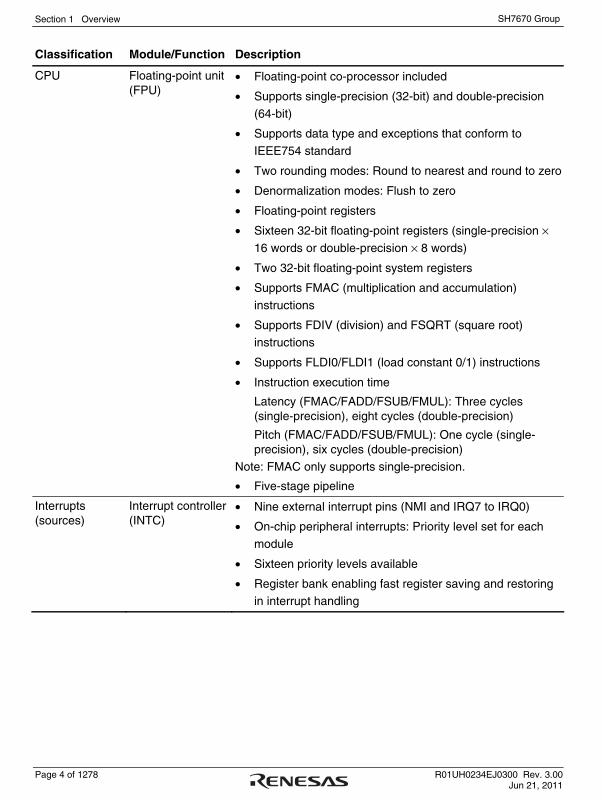
Section 1 Overview
Page 4 of 1278 R01UH0234EJ0300 Rev. 3.00 Jun 21, 2011
SH7670 Group
Classification Module/Function Description
CPU Floating-point unit (FPU)
• Floating-point co-processor included
• Supports single-precision (32-bit) and double-precision
(64-bit)
• Supports data type and exceptions that conform to
IEEE754 standard
• Two rounding modes: Round to nearest and round to zero
• Denormalization modes: Flush to zero
• Floating-point registers
• Sixteen 32-bit floating-point registers (single-precision ×
16 words or double-precision × 8 words)
• Two 32-bit floating-point system registers
• Supports FMAC (multiplication and accumulation)
instructions
• Supports FDIV (division) and FSQRT (square root)
instructions
• Supports FLDI0/FLDI1 (load constant 0/1) instructions
• Instruction execution time
Latency (FMAC/FADD/FSUB/FMUL): Three cycles (single-precision), eight cycles (double-precision)
Pitch (FMAC/FADD/FSUB/FMUL): One cycle (single-precision), six cycles (double-precision)
Note: FMAC only supports single-precision.
• Five-stage pipeline
Interrupts (sources)
Interrupt controller (INTC)
• Nine external interrupt pins (NMI and IRQ7 to IRQ0)
• On-chip peripheral interrupts: Priority level set for each
module
• Sixteen priority levels available
• Register bank enabling fast register saving and restoring
in interrupt handling

Section 1 Overview
R01UH0234EJ0300 Rev. 3.00 Page 5 of 1278 Jun 21, 2011
SH7670 Group
Classification Module/Function Description
External bus extension
Bus state controller (BSC)
• Address space for five areas (64 Mbytes each) and 32-bit
external bus
• The following features settable independently for each
area:
⎯ Bus size: 8, 16, or 32 bits (depending on area)
⎯ Access wait cycle count
⎯ Idle wait cycle setting (same area/different area)
⎯ Supports SRAM, SRAM with byte selection, and
SDRAM by specifying memory to be connected for
each area
⎯ Supports the PCMCIA interface
⎯ Chip select signal output to an applicable area (Timings of CS asserting and negating are selectable
by programming)
• SDRAM refreshing function
⎯ Supports auto-refreshing mode and self-refreshing
mode
• SDRAM burst access function
• For area 0, only big endian is supported
DMA Direct memory access controller (DMAC)
• Eight channels (External DMA requests available for two
of them)
• Can be activated by on-chip peripheral modules
• Burst mode and cycle steal mode
• Supports intermittent mode (16 or 64 cycles)
• Auto-reloading of transfer information

Section 1 Overview
Page 6 of 1278 R01UH0234EJ0300 Rev. 3.00 Jun 21, 2011
SH7670 Group
Classification Module/Function Description
Clock pulse generator (CPG)
• Clock mode: Input clock can be selected from external
input (EXTAL or CKIO) or crystal resonator (EXTAL/XTAL
or USB_X1/USB_X2).
• Three types of clocks generated
⎯ CPU clock:
200 MHz (maximum) (regular specifications)
133 MHz (maximum) (wide temperature
specifications)
⎯ Bus clock:
100 MHz (maximum) (regular specifications)
66 MHz (maximum) (wide temperature specifications)
⎯ Peripheral clock:
50 MHz (maximum) (regular specifications)
33 MHz (maximum) (wide temperature specifications)
Clock
Power-down modes
• Three power-down modes provided to reduce the current
consumption in this LSI
⎯ Sleep mode
⎯ Software standby mode
⎯ Module standby mode
Compare match timer (CMT)
• Two-channel 16-bit counter
• Four types of clocks selectable (Pφ/8, Pφ/32, Pφ/128, or
Pφ/512)
• Generates a compare match interrupt
Timer
Watchdog timer (WDT)
• One-channel watchdog timer
A counter overflow can reset this LSI

Section 1 Overview
R01UH0234EJ0300 Rev. 3.00 Page 7 of 1278 Jun 21, 2011
SH7670 Group
Classification Module/Function Description
Ethernet controller (EtherC)
• MAC (Media Access Control) function
⎯ Data frame assembly/deassembly (frame format
conforming to IEEE802.3)
⎯ CSMA/CD link management (for collision avoidance
and processing in case of collision)
⎯ CRC processing
⎯ On-chip FIFOs (512 bytes for transmission and
reception each)
⎯ Supports full-duplex data transmission and reception
⎯ Sends and receives short and long packets
• Conforms to the MII (Media Independent Interface)
standard
⎯ Converts an 8-bit data stream from the MAC layer to a
4-bit MII nibble stream
⎯ Station management (STA feature)
⎯ Eighteen TTL-level signals
⎯ Transfer rate: 10 or 100 Mbps
• Magic PacketTM with WOL (Wake On LAN) output
Advanced communication
DMAC for Ethernet controller (E-DMAC)
• Reduces CPU load using the descriptor management
system
• One channel for transfer from the EtherC receive FIFO to
the receive buffer
• One channel for transfer from the transmit buffer to the
EtherC transmit FIFO
• Allows 16-byte burst transfer for efficient use of the
system bus
• Supports single frame and multibuffer
• Calculates receive data checksum
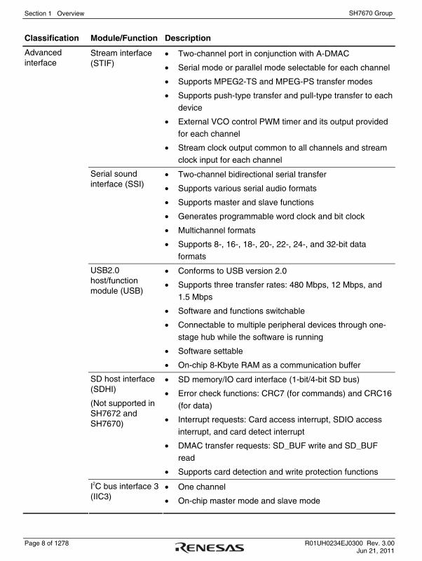
Section 1 Overview
Page 8 of 1278 R01UH0234EJ0300 Rev. 3.00 Jun 21, 2011
SH7670 Group
Classification Module/Function Description
Stream interface (STIF)
• Two-channel port in conjunction with A-DMAC
• Serial mode or parallel mode selectable for each channel
• Supports MPEG2-TS and MPEG-PS transfer modes
• Supports push-type transfer and pull-type transfer to each
device
• External VCO control PWM timer and its output provided
for each channel
• Stream clock output common to all channels and stream
clock input for each channel
Serial sound interface (SSI)
• Two-channel bidirectional serial transfer
• Supports various serial audio formats
• Supports master and slave functions
• Generates programmable word clock and bit clock
• Multichannel formats
• Supports 8-, 16-, 18-, 20-, 22-, 24-, and 32-bit data
formats
USB2.0 host/function module (USB)
• Conforms to USB version 2.0
• Supports three transfer rates: 480 Mbps, 12 Mbps, and
1.5 Mbps
• Software and functions switchable
• Connectable to multiple peripheral devices through one-
stage hub while the software is running
• Software settable
• On-chip 8-Kbyte RAM as a communication buffer
SD host interface (SDHI)
(Not supported in SH7672 and SH7670)
• SD memory/IO card interface (1-bit/4-bit SD bus)
• Error check functions: CRC7 (for commands) and CRC16
(for data)
• Interrupt requests: Card access interrupt, SDIO access
interrupt, and card detect interrupt
• DMAC transfer requests: SD_BUF write and SD_BUF
read
• Supports card detection and write protection functions
Advanced interface
I2C bus interface 3 (IIC3)
• One channel
• On-chip master mode and slave mode

Section 1 Overview
R01UH0234EJ0300 Rev. 3.00 Page 9 of 1278 Jun 21, 2011
SH7670 Group
Classification Module/Function Description
Host interface (HIF)
• On-chip 4-Kbyte buffer RAM (two 2-Kbyte banks)
• Parallel connection of buffer RAM and external device
with sixteen data pins
• Parallel connection of buffer RAM and the CPU of this LSI
with the internal bus
• A connected external device can access desired register
after the register index was specified (However,
addresses can be automatically updated during
continuous buffer RAM access)
• Endian switchable
• An interrupt can be requested to a connected external
device
• An internal interrupt can be requested to the CPU of this
LSI
• Allows booting from the buffer RAM by storing the instruction code beforehand from the external device in
the buffer RAM
Advanced interface
Serial communication interface with FIFO (SCIF)
• Three channels
• Clock synchronous mode or asynchronous mode
selectable
• Supports simultaneous transmission and reception (full-
duplex communication)
• Dedicated baud rate generator
• Separate 16-byte FIFO registers for transmission and
reception
• Modem control function (asynchronous mode)

Section 1 Overview
Page 10 of 1278 R01UH0234EJ0300 Rev. 3.00 Jun 21, 2011
SH7670 Group
Classification Module/Function Description
Encryption functions (AES, DES and 3DES)
(SH7671 and SH7670 support only DMAC function. They do not support encryption function.)
• Encryption/decryption engine can be activated by 2-
channel dedicated DMAC (A-DMAC) or CPU
• By reading the descriptor using the A-DMAC, continuous encryption/decryption available by switching the source
address (unprocessed data pointer), destination address
(processed data storage address), and various settings (including encryption/decryption algorithm,
encryption/decryption, ECB/CBC/OFB, keys, and IV) in
real time
• Block-by-block encryption and decryption enabled by
activation from the CPU
Message authentication code generating functions (HMAC-SHA-1, HMAC-SHA-224, and HMAC-SHA-256)
(Not supported in SH7671 and SH7670)
• By reading the descriptor using the A-DMAC, generation
of message authentication codes and checksum calculation in conjunction with encryption/decryption
processing are available
Encryption, hash, and error correction
Forward error correction (FEC)
• By reading the descriptor using the dedicated F-DMAC,
missing packets can be restored quickly by switching the source address (read packet pointer), destination address
(restoration packet storage address), and packet size in
real time
• Arbitrary values can be used for the read packet pointer, read packet count, restoration packet storage address,
and packet size
User break controller (UBC)
• Two break channels
• Addresses, data values, type of access, and data size
can be set as break conditions
Debugging function
User debugging interface (H-UDI)
• Supports E10A emulator
• JTAG-standard pin assignment
• Supports boundary scan
I/O ports • Eighty-six general input/output pins and eight general
input pins
• Input or output of I/O ports can be selected for each bit

Section 1 Overview
R01UH0234EJ0300 Rev. 3.00 Page 11 of 1278 Jun 21, 2011
SH7670 Group
Classification Module/Function Description
Package • P-FBGA1717-256 (0.8 pitch)
Power supply voltage • I/O: 3.3 ± (0.2) V, internal: 1.2 ± (0.1) V
Operating temperature (°C) • -20 to +70°C (regular specifications)
• -40 to +85°C (wide temperature specifications)
Notes: * Magic PacketTM is a registered trademark of Advanced Micro Devices, Inc.
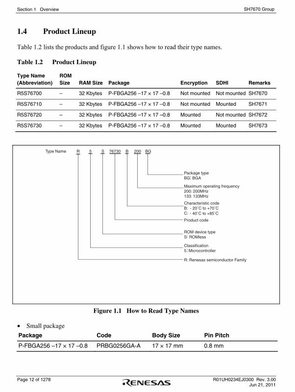
Section 1 Overview
Page 12 of 1278 R01UH0234EJ0300 Rev. 3.00 Jun 21, 2011
SH7670 Group
1.4 Product Lineup
Table 1.2 lists the products and figure 1.1 shows how to read their type names.
Table 1.2 Product Lineup
Type Name (Abbreviation)
ROM Size RAM Size Package Encryption SDHI Remarks
R5S76700 – 32 Kbytes P-FBGA256 –17 × 17 –0.8 Not mounted Not mounted SH7670
R5S76710 – 32 Kbytes P-FBGA256 –17 × 17 –0.8 Not mounted Mounted SH7671
R5S76720 – 32 Kbytes P-FBGA256 –17 × 17 –0.8 Mounted Not mounted SH7672
R5S76730 – 32 Kbytes P-FBGA256 –17 × 17 –0.8 Mounted Mounted SH7673
Type Name
R: Renesas semiconductor Family
Package typeBG BGA
Product code
Maximum operating frequency200: 200MHz 133: 133MHz
Characteristic codeB: - 20˚C to +70˚C C:
ROM device typeS ROMless
Classification5 Microcontroller
R 5 S 76730 B 200 BG
:
:
:
- 40˚C to +85˚C
Figure 1.1 How to Read Type Names
• Small package
Package Code Body Size Pin Pitch
P-FBGA256 –17 × 17 –0.8 PRBG0256GA-A 17 × 17 mm 0.8 mm
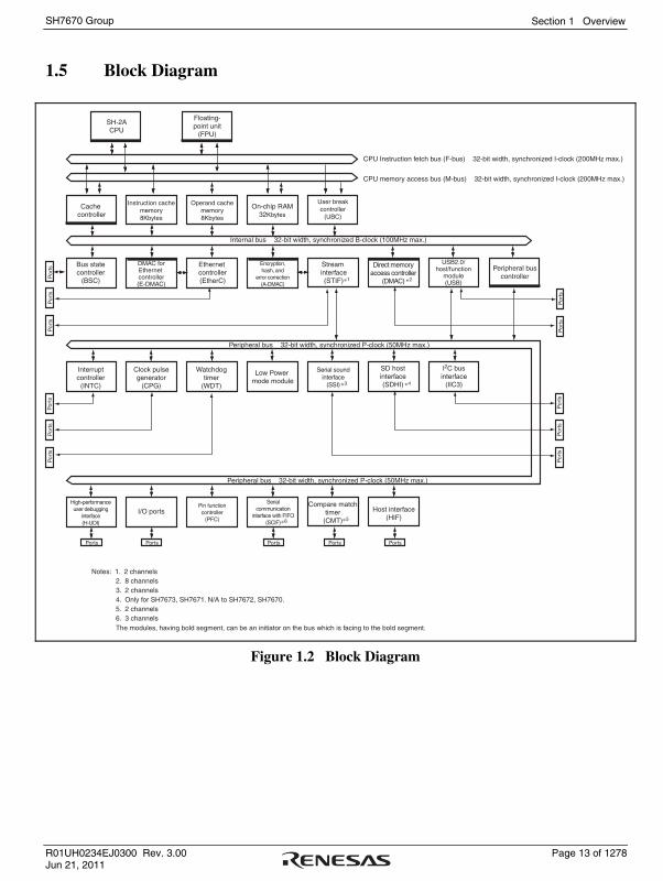
Section 1 Overview
R01UH0234EJ0300 Rev. 3.00 Page 13 of 1278 Jun 21, 2011
SH7670 Group
1.5 Block Diagram
Peripheral bus 32-bit width, synchronized P-clock (50MHz max.)
Peripheral bus 32-bit width, synchronized P-clock (50MHz max.)
Internal bus 32-bit width, synchronized B-clock (100MHz max.)
CPU Instruction fetch bus (F-bus) 32-bit width, synchronized I-clock (200MHz max.)
CPU memory access bus (M-bus) 32-bit width, synchronized I-clock (200MHz max.)
SH-2ACPU
Cache controller
Instruction cachememory8Kbytes
Operand cachememory8Kbytes
Bus statecontroller
(BSC)
Interruptcontroller
(INTC)
High-performanceuser debugging
interface(H-UDI)
I/O ports
Por
tsP
orts
Por
tsP
orts
Por
ts
Por
tsP
orts
Por
ts
Por
tsP
orts
Por
ts
PortsPorts Ports Ports Ports
Pin functioncontroller
(PFC)
Serialcommunication
interface with FIFO(SCIF)
Compare matchtimer
(CMT)
Host interface(HIF)
Notes: 1. 2 channels
The modules, having bold segment, can be an initiator on the bus which is facing to the bold segment.
2. 8 channels3. 2 channels4. Only for SH7673, SH7671. N/A to SH7672, SH7670.5. 2 channels6. 3 channels
Clock pulsegenerator
(CPG)
Watchdogtimer
(WDT)
Low Power mode module
Serial soundinterface
(SSI)
SD hostinterface(SDHI)
I2C businterface
(IIC3)
DMAC forEthernet controller(E-DMAC)
Ethernet controller(EtherC)
Encryption,hash, and
error correction(A-DMAC)
Stream interface(STIF)*1
*3
*6 *5
*4
*2
Direct memoryaccess controller
(DMAC)
USB2.0/host/function
module(USB)
Peripheral buscontroller
On-chip RAM32Kbytes
User breakcontroller
(UBC)
Floating- point unit
(FPU)
Figure 1.2 Block Diagram

Section 1 Overview
Page 14 of 1278 R01UH0234EJ0300 Rev. 3.00 Jun 21, 2011
SH7670 Group
1.6 Pin Assignments
1
A
B
C
D
E
F
G
H
J
K
L
M
N
P
R
T
U
V
W
2 3 4 5 6 7 8 9 10 11 12 13 14 15 16 17 18 19
SH7673/SH7672/SH7671/SH7670Top view
PA17/A17
A00PB04/ CE2A/IRQ2/
DACK1
PB00/WAIT/SDA
PB06/CS4
WE1/DQMLU/
WE
D09 D12 D15 D05 D02 A16 A13 A10 A07 A04
CS3
RAS CAS
PA18/A18
PA20/A20
PB05/CS5/CE1A/IRQ3/
TEND1
PB02/CE2B/IRQ0
RDPB07/
BSD08 D10 D14 D06 D03 D00 A14 A11 A08 A05 A02
A01
CKE
HIFMD/PA25/A25
PA21/A21
PA19/A19
PB03/CS6/CE1B/IRQ1/
DREQ1
PB01/IOIS16/
SCL
CS0WE0/
DQMLLD11 D13 D07 D04 D01 A15 A12 A09 A06 A03 RDWR CKIO
PC18/LNKSTA
PA24/A24
PA22/A22
VssQ_14 Vss_07 VccQ_14 Vcc_07 VssQ_13 VccQ_13 VccQ_12 VssQ_12 Vcc_06 Vss_06 VccQ_11 VssQ_11 VssQ_10WE3/
DQMUU/ICIOWR
WE2/DQMUL/ICIORD
D25
PC17/MDC
PC19/EXOUT
PA23/A23
VssQ_00 VssQ_09 D24 D26 D28
PC12/TX_EN
PC13/TX_CLK
PC20/WOL
VccQ_00 VccQ_10 D27 D29 D30
PC06/MII_TXD2
PC07/MII_TXD3
PC16/MDIO
Vss_00 VccQ_09 D31 D23 D22
PC15/CRS
PC05/MII_TXD1
PC11/TX_ER
Vcc_00 VccQ_08 VccQ_07 D21 D20
PC10/RX_CLK
PC14/COL
PC04/MII_TXD0
VssQ_01 VssQ_08 VssQ_07 D19 D18
PC08/RX_DV
PC03/MII_RXD3
PC09/RX_ER
VccQ_01 Vcc_05 D17 D16
PF07/ST0_D7/SSIWS0
PC02/MII_RXD2
PC01/MII_RXD1
PC00/MII_RXD0
VccQ_02 Vss_05PF06/
ST0_D6/SSIDATA0
PF05/ST0_D5/
RTS0
PF04/ST0_D4/
CTS0TESTMD ASEMD
PD07/IRQ7/
SDCLK
VssQ_02 VccQ_06
PF03/ST0_D3/
SCK0
PF02/ST0_D2/
RxD0
PF01/ST0_D1/
TxD0
PD06/IRQ6/
SDCMD
PD05/IRQ5/SDCD
PD04/IRQ4/SDWP
Vcc_01 VssQ_06
PF10/ST0_SYC/
DACK0
PF09/ST0_VLD/
DREQ0
PF00/ST0_D0
PD03/IRQ3/
SDDAT3
PD02/IRQ2/
SDDAT2
PD01/IRQ1/
SDDAT1
Vcc_02 Vcc_04
PF08/ST0_REQ
ST0_CLKIN/
SSISCK0
PF11/ST0_PWM/
TEND0
PD00/IRQ0/
SDDAT0
PG14/HIFD14
PG15/HIFD15
Vss_04
WDTOVF
ASEBRK/ASEBRKAK
ST0_VCO_CLKIN
PG12/HIFD12
PG13/HIFD13
PG11/HIFD11
Vss_01
VssQ_03Vss_02 VccQ_03 DG12 DV12 UV12 AV12 Vcc_03 Vss_03 VccQ_04 VccQ_05 VssQ_04 VssQ_05
MD_BW
NMI PLLVccPG10/
HIFD10PG09/
HIFD09
PG05/HIFD05
PG23/HIFCS
PG22/HIFRS
PG18/HIFDREQ
PG19/HIFINT
PG16/HIFEBL
UG12 AG12
PE04/ST1_D4/
CTS1
PE01/ST1_D1/
TxD1
PE09/ST1_VLD/
SCK2
ST1_VCO_CLKIN/
AUDIO_CLKTCK TDI
MD_CK1
MD_CK0 EXTAL
PG08/HIFD08
PG06/HIFD06
PG04/HIFD04
PG01/HIFD01
PG21/HIFWR
PG17/HIFRDY
DG33 VBUS AG33
PE06/ST1_D6/
SSIDATA1
USB_X1
PE07/ST1_D7/SSIWS1
PE03/ST1_D3/
SCK1
PE10/ST1_SYC/
CTS2
PE11/ST1_PWM/
RTS2
ST1_CLKIN/
SSISCK1RES TDO XTAL
PG07/HIFD07
PG03/HIFD03
PG02/HIFD02
PG00/HIFD00
PG20/HIFRD
DV33 DM DP AV33 REFRIN USB_X2
PE05/ST1_D5/
RTS1
PE02/ST1_D2/
RxD1
PE00/ST1_D0/
RxD2
PE08/ST1_REQ/
TxD2
ST_CLKOUT
TRST TMS PLLVssY
20
VssQ
VssQ
VssQVssQ VssQ
VssQ
VssQ
VssQ
VssQ
VssQ
VssQ
VssQ
VssQ
VssQ
VssQ
VssQ
← Location of index
Figure 1.3 Pin Assignments

Section 1 Overview
R01UH0234EJ0300 Rev. 3.00 Page 15 of 1278 Jun 21, 2011
SH7670 Group
1.7 Pin Functions
Table 1.3 Pin Functions
Classification Symbol I/O Name Function
Vcc I Power supply Power supply pin for the internal logic circuit. All the Vcc pins must be connected to the system power supply. This LSI does not operate correctly if there is a pin left open.
Vss I Ground Ground pin. All the Vss pins must be connected to the system power supply (0 V). This LSI does not operate correctly if there is a pin left open.
VccQ I Power supply Power supply pin for I/O pins. All the VccQ pins must be connected to the system power supply. This LSI does not operate correctly if there is a pin left open.
VssQ I Ground Ground pin. All the VssQ pins must be connected to the system power supply (0 V). This LSI does not operate correctly if there is a pin left open.
PLLVcc I Power supply Power supply pin for the PLL circuit. This pin must be connected to the system power supply.
Power supply
PLLVss I Ground Ground pin for the PLL circuit. This pin must be connected to the system power supply (0 V).
EXTAL I External clock Pin connected to a crystal resonator. An external clock signal may also be input to the EXTAL pin.
XTAL O Crystal resonator Pin connected to a crystal resonator
Clock
CKIO I/O System clock Pin to supply the system clock to external devices
MD_BW I Mode set Pin to set the operating mode. Do not change signal levels on this pin during operation.
Operating mode control
MD_CK1, MD_CK0
I Clock mode set Pins to set the clock operating mode. Do not change signal levels on these pins during operation.
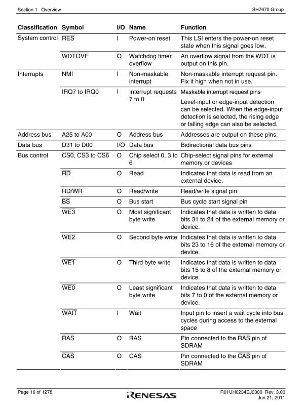
Section 1 Overview
Page 16 of 1278 R01UH0234EJ0300 Rev. 3.00 Jun 21, 2011
SH7670 Group
Classification Symbol I/O Name Function
RES I Power-on reset This LSI enters the power-on reset state when this signal goes low.
System control
WDTOVF O Watchdog timer overflow
An overflow signal from the WDT is output on this pin.
NMI I Non-maskable interrupt
Non-maskable interrupt request pin. Fix it high when not in use.
Interrupts
IRQ7 to IRQ0 I Interrupt requests 7 to 0
Maskable interrupt request pins
Level-input or edge-input detection can be selected. When the edge-input detection is selected, the rising edge or falling edge can also be selected.
Address bus A25 to A00 O Address bus Addresses are output on these pins.
Data bus D31 to D00 I/O Data bus Bidirectional data bus pins
CS0, CS3 to CS6 O Chip select 0, 3 to 6
Chip-select signal pins for external memory or devices
RD O Read Indicates that data is read from an external device.
RD/WR O Read/write Read/write signal pin
BS O Bus start Bus cycle start signal pin
WE3 O Most significant byte write
Indicates that data is written to data bits 31 to 24 of the external memory or device.
WE2 O Second byte write Indicates that data is written to data bits 23 to 16 of the external memory or device.
WE1 O Third byte write Indicates that data is written to data bits 15 to 8 of the external memory or device.
WE0 O Least significant byte write
Indicates that data is written to data bits 7 to 0 of the external memory or device.
WAIT I Wait Input pin to insert a wait cycle into bus cycles during access to the external space
RAS O RAS Pin connected to the RAS pin of SDRAM
Bus control
CAS O CAS Pin connected to the CAS pin of SDRAM

Section 1 Overview
R01UH0234EJ0300 Rev. 3.00 Page 17 of 1278 Jun 21, 2011
SH7670 Group
Classification Symbol I/O Name Function
CKE O Clock enable Pin connected to the CKE pin of SDRAM
DQMUU O Most significant byte select
Selects data bus bits 31 to 24 of SDRAM.
DQMUL O Second byte select
Selects data bus bits 23 to 16 of SDRAM.
DQMLU O Third byte select Selects data bus bits 15 to 8 of SDRAM.
DQMLL O Least significant byte select
Selects data bus bits 7 to 0 of SDRAM.
CE1A O PCMCIA card select (lower)
Chip enable signal pin for PCMCIA connected to area 5
CE1B O PCMCIA card select (lower)
Chip enable signal pin for PCMCIA connected to area 6
CE2A O PCMCIA card select (upper)
Chip enable signal pin for PCMCIA connected to area 5
CE2B O PCMCIA card select (upper)
Chip enable signal pin for PCMCIA connected to area 6
ICIOWR O PCMCIA I/O write strobe
Pin connected to the PCMCIA I/O write strobe
ICIORD O PCMCIA I/O read strobe
Pin connected to the PCMCIA I/O read strobe
WE O PCMCIA memory write strobe
Pin connected to the PCMCIA memory write strobe
Bus control
IOIS16 I PCMCIA dynamic bus sizing
Indicates the 16-bit I/O of PCMCIA in little-endian mode. Fix this pin low in big-endian mode.
DREQ0, DREQ1 I DMA-transfer request
Input pins to receive external requests for DMA transfer
DACK0, DACK1 O DMA-transfer request acknowledge
Output pins for signals indicating acknowledge of external requests from external devices
Direct memory access controller (DMAC)
TEND0, TEND1 O DMA-transfer end output
Output pins for DMA transfer end
CRS I Carrier sense Carrier sensing pin
COL I Collision Collision detecting pin
Ethernet controller (EtherC)
MII_TXD3 to MII_TXD0
O Transmit data 4-bit transmit data pins
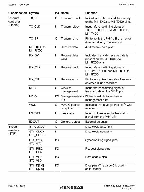
Section 1 Overview
Page 18 of 1278 R01UH0234EJ0300 Rev. 3.00 Jun 21, 2011
SH7670 Group
Classification Symbol I/O Name Function
TX_EN O Transmit enable Indicates that transmit data is ready on the MII_TXD3 to MII_TXD0 pins.
TX_CLK I Transmit clock Input reference timing signal of TX_EN, TX_ER, and MII_TXD3 to MII_TXD0
TX_ER O Transmit error Pin to notify the PHY-LSI of an error detected during transmission
MII_RXD3 to MII_RXD0
I Receive data 4-bit receive data pins
RX_DV I Receive data valid
Indicates that valid receive data is present on the MII_RXD3 to MII_RXD0 pins
RX_CLK I Receive clock Input reference timing signal of RX_DV, RX_ER, and MII_RXD3 to MII_RXD0
RX_ER I Receive error Pin to recognize the state of an error detected during reception
MDC O Clock for management
Input reference timing signal of transfer data on the MDIO pin
MDIO I/O Management data I/O
Bidirectional pin to exchange management data
WOL O MAGIC packet reception
Indicates that a Magic PacketTM* was received.
LNKSTA I Link status Input pin to receive the link status signal from the PHY-LSI
Ethernet controller (EtherC)
EXOUT O General output External output pin
ST_CLKOUT O Data clock output pin
ST1_CLKIN, ST0_CLKIN
I Data clock input pins
ST1_SYC, ST0_SYC
I/O Synchronizing signal pins
ST1_REQ, ST0_REQ
I/O Request signal pins
ST1_VLD, ST0_VLD
I/O Data enable pins
Stream interface (STIF)
ST1_D[7:0], ST0_D[7:0]
I/O Data pins (The value 0 is used in serial mode)

Section 1 Overview
R01UH0234EJ0300 Rev. 3.00 Page 19 of 1278 Jun 21, 2011
SH7670 Group
Classification Symbol I/O Name Function
ST1_VCO_CLKIN, ST0_VCO_CLKIN
I VCX0 clock pins Stream interface (STIF) ST1_PWM,
ST0_PWM O PWM output pins
SSIDATA1, SSIDATA0
I/O SSI data I/O Serial data I/O pins
SSISCK1, SSISCK0
I/O SSI clock I/O Serial clock I/O pins
SSIWS1, SSIWS0 I/O SSI clock LR I/O Word select I/O pins
Serial sound interface (SSI)
AUDIO_CLK I External clock for SSI audio
The external clock for audio is input to this pin.
DP I/O USB D+ data USB bus D+ data pin
DM I/O USB D- data USB bus D- data pin
VBUS I VBUS input Connect this pin to VBUS of the USB bus.
REFRIN I Reference input Connect this pin to AG33 through a resistor of 5.6 kΩ ±1%.
USB_X1 I
USB_X2 O
Crystal resonator/external clock input for USB
Pins connected to the crystal resonator for USB. When an external clock is used, connect it to the USB_1 pin with the USB_2 pin open.
AV33 I Analog power supply for transceiver
Power supply pin for the core (3.3 V (Typ.) supplied)
AG33 I Analog ground for transceiver
Ground pin for the core
AV12 I Analog power supply for transceiver
Power supply pin for the core (1.2 V (Typ.) supplied)
AG12 I Analog ground for transceiver
Ground pin for the core
DV33 I Power supply for transceiver pins
Power supply pin for pins (3.3 V (Typ.) supplied)
DG33 I Ground for transceiver pins
Ground pin for transceiver pins
USB2.0 host/function module (USB)
DV12 I Power supply for transceiver pins
Power supply pin for transceiver pins (1.2 V (Typ.) supplied)
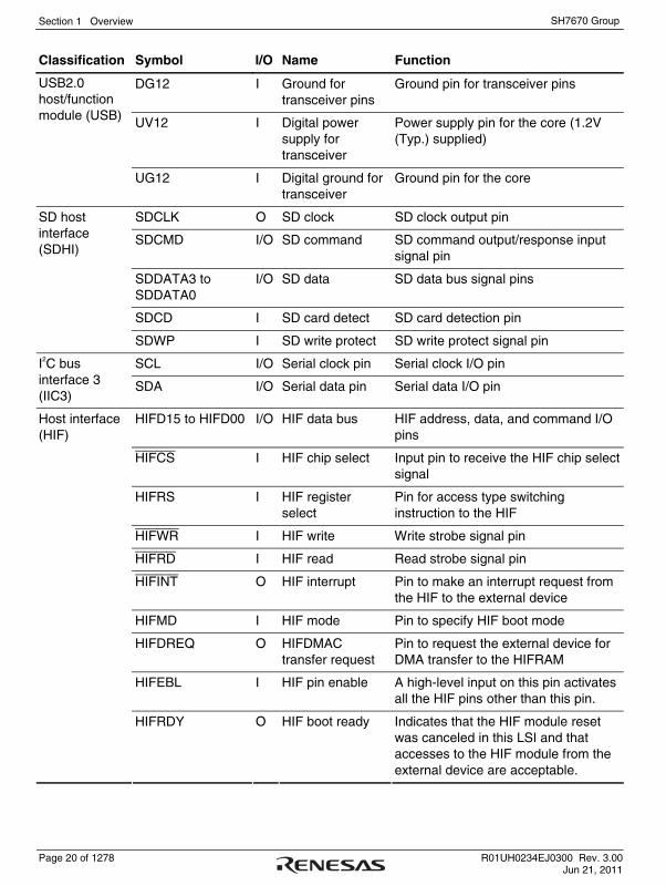
Section 1 Overview
Page 20 of 1278 R01UH0234EJ0300 Rev. 3.00 Jun 21, 2011
SH7670 Group
Classification Symbol I/O Name Function
DG12 I Ground for transceiver pins
Ground pin for transceiver pins
UV12 I Digital power supply for transceiver
Power supply pin for the core (1.2V (Typ.) supplied)
USB2.0 host/function module (USB)
UG12 I Digital ground for transceiver
Ground pin for the core
SDCLK O SD clock SD clock output pin
SDCMD I/O SD command SD command output/response input signal pin
SDDATA3 to SDDATA0
I/O SD data SD data bus signal pins
SDCD I SD card detect SD card detection pin
SD host interface (SDHI)
SDWP I SD write protect SD write protect signal pin
SCL I/O Serial clock pin Serial clock I/O pin I2C bus interface 3 (IIC3)
SDA I/O Serial data pin Serial data I/O pin
HIFD15 to HIFD00 I/O HIF data bus HIF address, data, and command I/O pins
HIFCS I HIF chip select Input pin to receive the HIF chip select signal
HIFRS I HIF register select
Pin for access type switching instruction to the HIF
HIFWR I HIF write Write strobe signal pin
HIFRD I HIF read Read strobe signal pin
HIFINT O HIF interrupt Pin to make an interrupt request from the HIF to the external device
HIFMD I HIF mode Pin to specify HIF boot mode
HIFDREQ O HIFDMAC transfer request
Pin to request the external device for DMA transfer to the HIFRAM
HIFEBL I HIF pin enable A high-level input on this pin activates all the HIF pins other than this pin.
Host interface (HIF)
HIFRDY O HIF boot ready Indicates that the HIF module reset was canceled in this LSI and that accesses to the HIF module from the external device are acceptable.
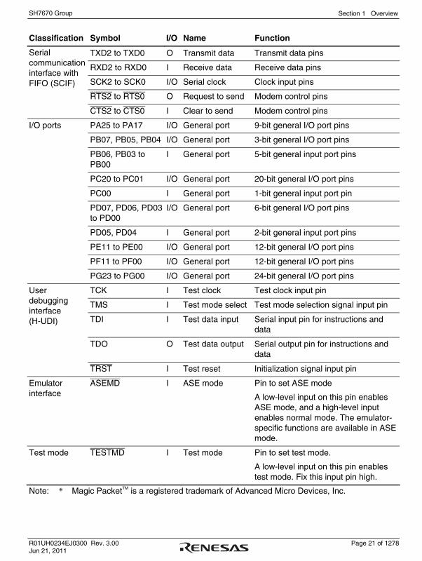
Section 1 Overview
R01UH0234EJ0300 Rev. 3.00 Page 21 of 1278 Jun 21, 2011
SH7670 Group
Classification Symbol I/O Name Function
TXD2 to TXD0 O Transmit data Transmit data pins
RXD2 to RXD0 I Receive data Receive data pins
SCK2 to SCK0 I/O Serial clock Clock input pins
RTS2 to RTS0 O Request to send Modem control pins
Serial communication interface with FIFO (SCIF)
CTS2 to CTS0 I Clear to send Modem control pins
PA25 to PA17 I/O General port 9-bit general I/O port pins
PB07, PB05, PB04 I/O General port 3-bit general I/O port pins
PB06, PB03 to PB00
I General port 5-bit general input port pins
PC20 to PC01 I/O General port 20-bit general I/O port pins
PC00 I General port 1-bit general input port pin
PD07, PD06, PD03 to PD00
I/O General port 6-bit general I/O port pins
PD05, PD04 I General port 2-bit general input port pins
PE11 to PE00 I/O General port 12-bit general I/O port pins
PF11 to PF00 I/O General port 12-bit general I/O port pins
I/O ports
PG23 to PG00 I/O General port 24-bit general I/O port pins
TCK I Test clock Test clock input pin
TMS I Test mode select Test mode selection signal input pin
TDI I Test data input Serial input pin for instructions and data
TDO O Test data output Serial output pin for instructions and data
User debugging interface (H-UDI)
TRST I Test reset Initialization signal input pin
Emulator interface
ASEMD I ASE mode Pin to set ASE mode
A low-level input on this pin enables ASE mode, and a high-level input enables normal mode. The emulator-specific functions are available in ASE mode.
Test mode TESTMD I Test mode Pin to set test mode.
A low-level input on this pin enables test mode. Fix this input pin high.
Note: * Magic PacketTM is a registered trademark of Advanced Micro Devices, Inc.

Section 1 Overview
Page 22 of 1278 R01UH0234EJ0300 Rev. 3.00 Jun 21, 2011
SH7670 Group
Table 1.4 List of I/O Attributes of Each Pin
Pin Number Function Name I/O Attribute
A1 PA17/A17 IO/O
A2 A00 O
A3 PB04/CE2A/IRQ2/DACK1 IO/O/I/O
A4 PB00/WAIT/SDA I/I/IO
A5 PB06/CS4 I/O
A6 WE1/DQMLU/WE O/O/O
A7 D09 IO
A8 D12 IO
A9 D15 IO
A10 D05 IO
A11 D02 IO
A12 A16 O
A13 A13 O
A14 A10 O
A15 A07 O
A16 A04 O
A17 A01 O
A18 RAS O
A19 CAS O
A20 VssQ Power
B1 PA19/A19 IO/O
B2 PA18/A18 IO/O
B3 PB05/CS5/CE1A/IRQ3/TEND1 IO/O/O/I/O
B4 PB02/CE2B/IRQ0 I/O/I
B5 RD O
B6 PB07/BS IO/O
B7 D08 IO
B8 D10 IO
B9 D14 IO
B10 D06 IO
B11 D03 IO

Section 1 Overview
R01UH0234EJ0300 Rev. 3.00 Page 23 of 1278 Jun 21, 2011
SH7670 Group
Pin Number Function Name I/O Attribute
B12 D00 IO
B13 A14 O
B14 A11 O
B15 A08 O
B16 A05 O
B17 A02 O
B18 CS3 O
B19 VSSQ Power
B20 CKE O
C1 PA22/A22 IO/O
C2 PA21/A21 IO/O
C3 PA20/A20 IO/O
C4 PB03/CS6/CE1B/IRQ1/DREQ1 I/O/O/I/I
C5 PB01/IOIS16/SCL I/I/IO
C6 CS0 O
C7 WE0/DQMLL O/O
C8 D11 IO
C9 D13 IO
C10 D07 IO
C11 D04 IO
C12 D01 IO
C13 A15 O
C14 A12 O
C15 A09 O
C16 A06 O
C17 A03 O
C18 VSSQ Power
C19 RDWR O
C20 CKIO IO
D1 HIFMD/PA25/A25 I/IO/o
D2 PA24/A24 IO/O
D3 PA23/A23 IO/O
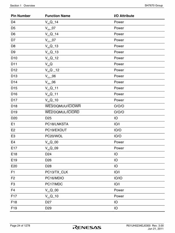
Section 1 Overview
Page 24 of 1278 R01UH0234EJ0300 Rev. 3.00 Jun 21, 2011
SH7670 Group
Pin Number Function Name I/O Attribute
D4 VSSQ_14 Power
D5 VSS_07 Power
D6 VCCQ_14 Power
D7 VCC_07 Power
D8 VSSQ_13 Power
D9 VCCQ_13 Power
D10 VCCQ_12 Power
D11 VSSQ Power
D12 VSSQ _12 Power
D13 VCC_06 Power
D14 VSS_06 Power
D15 VCCQ_11 Power
D16 VSSQ_11 Power
D17 VSSQ_10 Power
D18 WE3/DQMUU/ICIOWR O/O/O
D19 WE2/DQMUL/ICIORD O/O/O
D20 D25 IO
E1 PC18/LNKSTA IO/I
E2 PC19/EXOUT IO/O
E3 PC20/WOL IO/O
E4 VSSQ_00 Power
E17 VSSQ_09 Power
E18 D24 IO
E19 D26 IO
E20 D28 IO
F1 PC13/TX_CLK IO/I
F2 PC16/MDIO IO/IO
F3 PC17/MDC IO/I
F4 VCCQ_00 Power
F17 VCCQ_10 Power
F18 D27 IO
F19 D29 IO

Section 1 Overview
R01UH0234EJ0300 Rev. 3.00 Page 25 of 1278 Jun 21, 2011
SH7670 Group
Pin Number Function Name I/O Attribute
F20 D30 IO
G1 PC07/MII_TXD3 IO/O
G2 PC11/TX_ER IO/O
G3 PC12/TX_EN IO/O
G4 VSS_00 Power
G17 VCCQ_09 Power
G18 D31 IO
G19 D23 IO
G20 D22 IO
H1 PC04/MII_TXD0 IO/O
H2 PC05/MILL_TXD1 IO/O
H3 PC06/MII_TXD2 IO/O
H4 VCC_00 Power
H17 VCCQ_08 Power
H18 VCCQ_07 Power
H19 D21 IO
H20 D20 IO
J1 PC10/RX_CLK IO/I
J2 PC14/COL IO/I
J3 PC15/CRS IO/I
J4 VSSQ_01 Power
J17 VSSQ_08 Power
J18 VSSQ_07 Power
J19 D19 IO
J20 D18 IO
K1 PC03/MII_RXD3 IO/I
K2 PC08/RX_DV IO/I
K3 PC09/RX_ER IO/I
K4 VCCQ_01 Power
K17 VCC_05 Power
K18 VSSQ Power
K19 D17 IO

Section 1 Overview
Page 26 of 1278 R01UH0234EJ0300 Rev. 3.00 Jun 21, 2011
SH7670 Group
Pin Number Function Name I/O Attribute
K20 D16 IO
L1 PC00/MII_RXD0 I/I
L2 PC01/MII_RXD1 IO/I
L3 PC02/MII_RXD2 IO/I
L4 VCCQ_02 Power
L17 VSS_05 Power
L18 PF05/ST0_D5/RTS0 IO/IO/IO
L19 PF06/ST0_D6/SSIDATA0 IO/IO/IO
L20 PF07/ST0_D7/SSIWS0 IO/IO/IO
M1 TESTMD I
M2 ASEMD I
M3 PD07/IRQ7/SDCLK IO/I/O
M4 VSSQ Power
M17 VSSQ Power
M18 PF02/ST0_D2/RxD0 IO/IO/I
M19 PF03/ST0_D3/SCK0 IO/IO/IO
M20 PF04/ST0_D4/CTS0 IO/IO/IO
N1 PD04/IRQ4/SDWP I/I/I
N2 PD05/IRQ5/SDCD I/I/I
N3 PD06/IRQ6/SDCMD IO/I/IO
N4 VSSQ_02 Power
N17 VCCQ_06 Power
N18 PF01/ST0_D1/TxD0 IO/IO/O
N19 PF10/ST0_SYC/DACK0 IO/O/O
N20 PF00/ST0_D0 IO/IO
P1 PD01/IRQ1/SDDAT1 IO/I/I
P2 PD02/IRQ2/SDDAT2 IO/I/IO
P3 PD03/IRQ3/SDDAT3 IO/I/IO
P4 VCC_01 Power
P17 VSSQ_06 Power
P18 PF11/ST0_PWM/TEND0 IO/O/O
P19 PF08/ST0_REQ IO/IO

Section 1 Overview
R01UH0234EJ0300 Rev. 3.00 Page 27 of 1278 Jun 21, 2011
SH7670 Group
Pin Number Function Name I/O Attribute
P20 PF09_ST0_VLD/DREQ0 IO/IO/I
R1 PG14/HIFD14 IO/IO
R2 PG15/HIFD15 IO/IO
R3 PD00/IRQ0/SDDAT0 IO/I/IO
R4 VCC_02 Power
R17 VCC_04 Power
R18 WDTOVF O
R19 ST0_CLKIN/SSISCK0 I/IO
R20 ST0_VCO_CLKIN I
T1 PG11/HIFD11 IO/IO
T2 PG12/HIFD12 IO/IO
T3 PG13/HIFD13 IO/IO
T4 VSS_01 Power
T17 VSS_04 Power
T18 VSSQ Power
T19 MD_BW I
T20 ASEBRK/ASEBRKAK I/O
U1 PG09/HIFD09 IO/IO
U2 PG10/HIFD10 IO/IO
U3 VSSQ Power
U4 VSS_02 Power
U5 VSSQ_03 Power
U6 VCCQ_03 Power
U7 VSSQ Power
U8 DG12 Power
U9 DV12 Power
U10 UV12 Power
U11 AV12 Power
U12 VCC_03 Power
U13 VSS_03 Power
U14 VCCQ_04 Power
U15 VCCQ_05 Power

Section 1 Overview
Page 28 of 1278 R01UH0234EJ0300 Rev. 3.00 Jun 21, 2011
SH7670 Group
Pin Number Function Name I/O Attribute
U16 VSSQ_04 Power
U17 VSSQ _05 Power
U18 MD_CK1 I
U19 NMI I
U20 PLLVCC Power
V1 PG07/HIFD07 IO/IO
V2 VSSQ Power
V3 PG04/HIFD04 IO/IO
V4 PG01/HIFD01 IO/IO
V5 PG22/HIFRS IO/I
V6 PG17/HIFRDY IO/O
V7 VSSQ Power
V8 VSSQ Power
V9 VSSQ Power
V10 UG12 Power
V11 AG12 Power
V12 PE07/ST1_D7/SSIWS1 IO/IO/IO
V13 PE06/ST1_D6/SSIDATA1 IO/IO/IO
V14 PE01/ST1_D1/TxD1 IO/IO/O
V15 PE03/ST1_D3/SCK1 IO/O/IO
V16 ST1_VCO_CLKIN/AUDIO_CLK I/I
V17 TCK I
V18 TDI I
V19 MD_CK0 I
V20 EXTAL I
W1 VSSQ Power
W2 PG06/HIFD06 IO/IO
W3 PG03/HIFD03 IO/IO
W4 PG00/HIFD00 IO/IO
W5 PG21/HIFWR IO/I
W6 PG18/HIFDREQ IO/O
W7 PG16/HIFEBL IO/I

Section 1 Overview
R01UH0234EJ0300 Rev. 3.00 Page 29 of 1278 Jun 21, 2011
SH7670 Group
Pin Number Function Name I/O Attribute
W8 DG33 Power
W9 VBUS I
W10 AG33 Power
W11 VSSQ Power
W12 USB_X1 I
W13 PE05/ST1_D5/RTS1 IO/IO/IO
W14 PE02/ST1_D2/RxD1 IO/IO/I
W15 PE10/ST1_SYC/CTS2 IO/IO/IO
W16 PE11/ST1_PWM/RTS2 IO/O/IO
W17 ST1_CLKIN/SSISCK1 I/IO
W18 RES I
W19 TDO O
W20 XTAL O
Y1 PG08/HIFD08 IO/IO
Y2 PG05/HIFD05 IO/IO
Y3 PG02/HIFD02 IO/IO
Y4 PG23/HIFCS IO/I
Y5 PG20/HIFRD IO/I
Y6 PG19/HIFINT IO/O
Y7 DV33 Power
Y8 DM IO
Y9 DP IO
Y10 AV33 Power
Y11 REFRIN I
Y12 USB_X2 O
Y13 PE04/ST1_D4/CTS1 IO/IO/IO
Y14 PE09/ST1_VLD/SCK2 IO/IO/IO
Y15 PE00/ST1_D0/RxD2 IO/IO/I
Y16 PE08/ST1_REQ/TxD2 IO/IO/O
Y17 ST_CLKOUT O
Y18 TRST I
Y19 TMS I
Y20 PLLVSS Power

Section 1 Overview
Page 30 of 1278 R01UH0234EJ0300 Rev. 3.00 Jun 21, 2011
SH7670 Group
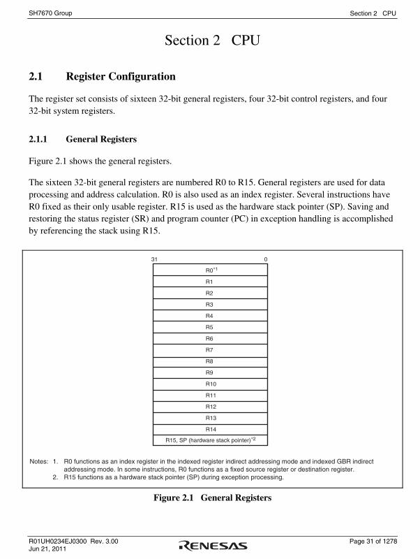
Section 2 CPU
R01UH0234EJ0300 Rev. 3.00 Page 31 of 1278 Jun 21, 2011
SH7670 Group
Section 2 CPU
2.1 Register Configuration
The register set consists of sixteen 32-bit general registers, four 32-bit control registers, and four 32-bit system registers.
2.1.1 General Registers
Figure 2.1 shows the general registers.
The sixteen 32-bit general registers are numbered R0 to R15. General registers are used for data processing and address calculation. R0 is also used as an index register. Several instructions have R0 fixed as their only usable register. R15 is used as the hardware stack pointer (SP). Saving and restoring the status register (SR) and program counter (PC) in exception handling is accomplished by referencing the stack using R15.
31 0
R0*1
R1
R2
R3
R4
R5
R6
R7
R8
R9
R10
R11
R12
R13
R14
R15, SP (hardware stack pointer)*2
Notes: 1. R0 functions as an index register in the indexed register indirect addressing mode and indexed GBR indirect addressing mode. In some instructions, R0 functions as a fixed source register or destination register.
2. R15 functions as a hardware stack pointer (SP) during exception processing.
Figure 2.1 General Registers

Section 2 CPU
Page 32 of 1278 R01UH0234EJ0300 Rev. 3.00 Jun 21, 2011
SH7670 Group
2.1.2 Control Registers
The control registers consist of four 32-bit registers: the status register (SR), the global base register (GBR), the vector base register (VBR), and the jump table base register (TBR).
The status register indicates instruction processing states.
The global base register functions as a base address for the GBR indirect addressing mode to transfer data to the registers of on-chip peripheral modules.
The vector base register functions as the base address of the exception handling vector area (including interrupts).
The jump table base register functions as the base address of the function table area.
31 01TS
23456789I[3:0]QM
1314CSBO Status register (SR)
31 0GBR Global base register (GBR)
31VBR Vector base register (VBR)
0
31TBR Jump table base register (TBR)
0
Figure 2.2 Control Registers
(1) Status Register (SR)
31 30 29 28 27 26 25 24 23 22 21 20 19 18 17 16
15 14 13 12 11 10 9 8 7 6 5 4 3 2 1 0
0 0 0 0 0 0 0 0 0 0 0 0 0 0 0 0R R R R R R R R R R R R R R R R
0 0 0 0 0 0 - - 1 1 1 1 0 0 - -R R/W R/W R R R R/W R/W R/W R/W R/W R/W R R R/W R/W
Bit:
Initial value:R/W:
Bit:
Initial value:R/W:
- - - - - - - - - - - - - - - -
- BO CS - - - M Q I[3:0] - - S T
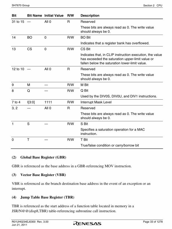
Section 2 CPU
R01UH0234EJ0300 Rev. 3.00 Page 33 of 1278 Jun 21, 2011
SH7670 Group
Bit Bit Name Initial Value R/W Description
31 to 15 — All 0 R Reserved
These bits are always read as 0. The write value should always be 0.
14 BO 0 R/W BO Bit
Indicates that a register bank has overflowed.
13 CS 0 R/W CS Bit
Indicates that, in CLIP instruction execution, the value has exceeded the saturation upper-limit value or fallen below the saturation lower-limit value.
12 to 10 — All 0 R Reserved
These bits are always read as 0. The write value should always be 0.
9 M — R/W
8 Q — R/W
M Bit
Q Bit
Used by the DIV0S, DIV0U, and DIV1 instructions.
7 to 4 I[3:0] 1111 R/W Interrupt Mask Level
3, 2 — All 0 R Reserved
These bits are always read as 0. The write value should always be 0.
1 S — R/W S Bit
Specifies a saturation operation for a MAC instruction.
0 T — R/W T Bit
True/false condition or carry/borrow bit
(2) Global Base Register (GBR)
GBR is referenced as the base address in a GBR-referencing MOV instruction.
(3) Vector Base Register (VBR)
VBR is referenced as the branch destination base address in the event of an exception or an interrupt.
(4) Jump Table Base Register (TBR)
TBR is referenced as the start address of a function table located in memory in a JSR/N@@(disp8,TBR) table-referencing subroutine call instruction.

Section 2 CPU
Page 34 of 1278 R01UH0234EJ0300 Rev. 3.00 Jun 21, 2011
SH7670 Group
2.1.3 System Registers
The system registers consist of four 32-bit registers: the high and low multiply and accumulate registers (MACH and MACL), the procedure register (PR), and the program counter (PC). MACH and MACL store the results of multiply or multiply and accumulate operations. PR stores the return address from a subroutine procedure. PC indicates the program address being executed and controls the flow of the processing.
31 0
31 0
31PC
PR
MACLMACH
Multiply and accumulate register high (MACH) and multiplyand accumulate register low (MACL):Store the results of multiply or multiply and accumulate operations.
Procedure register (PR):Stores the return address from a subroutine procedure.
Program counter (PC):Indicates the four bytes ahead of the current instruction.
0
Figure 2.3 System Registers
(1) Multiply and Accumulate Register High (MACH) and Multiply and Accumulate Register Low (MACL)
MACH and MACL are used as the addition value in a MAC instruction, and store the result of a MAC or MUL instruction.
(2) Procedure Register (PR)
PR stores the return address of a subroutine call using a BSR, BSRF, or JSR instruction, and is referenced by a subroutine return instruction (RTS).
(3) Program Counter (PC)
PC indicates the address of the instruction being executed.
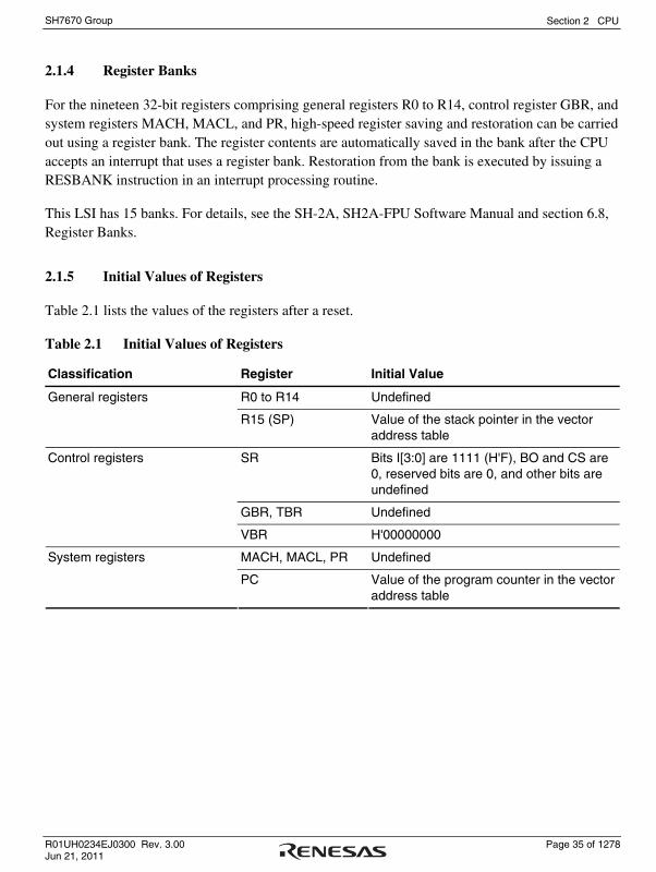
Section 2 CPU
R01UH0234EJ0300 Rev. 3.00 Page 35 of 1278 Jun 21, 2011
SH7670 Group
2.1.4 Register Banks
For the nineteen 32-bit registers comprising general registers R0 to R14, control register GBR, and system registers MACH, MACL, and PR, high-speed register saving and restoration can be carried out using a register bank. The register contents are automatically saved in the bank after the CPU accepts an interrupt that uses a register bank. Restoration from the bank is executed by issuing a RESBANK instruction in an interrupt processing routine.
This LSI has 15 banks. For details, see the SH-2A, SH2A-FPU Software Manual and section 6.8, Register Banks.
2.1.5 Initial Values of Registers
Table 2.1 lists the values of the registers after a reset.
Table 2.1 Initial Values of Registers
Classification Register Initial Value
R0 to R14 Undefined General registers
R15 (SP) Value of the stack pointer in the vector address table
SR Bits I[3:0] are 1111 (H'F), BO and CS are 0, reserved bits are 0, and other bits are undefined
GBR, TBR Undefined
Control registers
VBR H'00000000
MACH, MACL, PR Undefined System registers
PC Value of the program counter in the vector address table

Section 2 CPU
Page 36 of 1278 R01UH0234EJ0300 Rev. 3.00 Jun 21, 2011
SH7670 Group
2.2 Data Formats
2.2.1 Data Format in Registers
Register operands are always longwords (32 bits). If the size of memory operand is a byte (8 bits) or a word (16 bits), it is changed into a longword by expanding the sign-part when loaded into a register.
31 0
Longword
Figure 2.4 Data Format in Registers
2.2.2 Data Formats in Memory
Memory data formats are classified into bytes, words, and longwords. Memory can be accessed in 8-bit bytes, 16-bit words, or 32-bit longwords. A memory operand of fewer than 32 bits is stored in a register in sign-extended or zero-extended form.
A word operand should be accessed at a word boundary (an even address of multiple of two bytes: address 2n), and a longword operand at a longword boundary (an even address of multiple of four bytes: address 4n). Otherwise, an address error will occur. A byte operand can be accessed at any address.
Only big-endian byte order can be selected for the data format.
Data formats in memory are shown in figure 2.5.
31 01523 7
Byte Byte Byte Byte
WordWordAddress 2n
Address 4n Longword
Address m Address m + 2
Address m + 1 Address m + 3
Big endian
Figure 2.5 Data Formats in Memory

Section 2 CPU
R01UH0234EJ0300 Rev. 3.00 Page 37 of 1278 Jun 21, 2011
SH7670 Group
2.2.3 Immediate Data Format
Byte (8-bit) immediate data is located in an instruction code. Immediate data accessed by the MOV, ADD, and CMP/EQ instructions is sign-extended and handled in registers as longword data. Immediate data accessed by the TST, AND, OR, and XOR instructions is zero-extended and handled as longword data. Consequently, AND instructions with immediate data always clear the upper 24 bits of the destination register.
20-bit immediate data is located in the code of a MOVI20 or MOVI20S 32-bit transfer instruction. The MOVI20 instruction stores immediate data in the destination register in sign-extended form. The MOVI20S instruction shifts immediate data by eight bits in the upper direction, and stores it in the destination register in sign-extended form.
Word or longword immediate data is not located in the instruction code, but rather is stored in a memory table. The memory table is accessed by an immediate data transfer instruction (MOV) using the PC relative addressing mode with displacement.
See examples given in section 2.3.1 (10), Immediate Data.
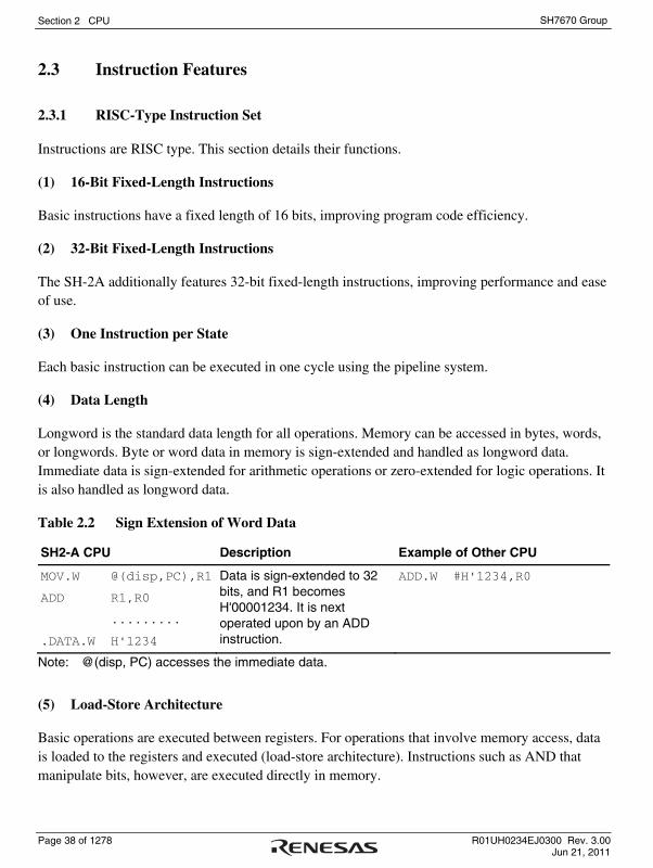
Section 2 CPU
Page 38 of 1278 R01UH0234EJ0300 Rev. 3.00 Jun 21, 2011
SH7670 Group
2.3 Instruction Features
2.3.1 RISC-Type Instruction Set
Instructions are RISC type. This section details their functions.
(1) 16-Bit Fixed-Length Instructions
Basic instructions have a fixed length of 16 bits, improving program code efficiency.
(2) 32-Bit Fixed-Length Instructions
The SH-2A additionally features 32-bit fixed-length instructions, improving performance and ease of use.
(3) One Instruction per State
Each basic instruction can be executed in one cycle using the pipeline system.
(4) Data Length
Longword is the standard data length for all operations. Memory can be accessed in bytes, words, or longwords. Byte or word data in memory is sign-extended and handled as longword data. Immediate data is sign-extended for arithmetic operations or zero-extended for logic operations. It is also handled as longword data.
Table 2.2 Sign Extension of Word Data
SH2-A CPU Description Example of Other CPU
MOV.W @(disp,PC),R1
ADD R1,R0
.........
.DATA.W H'1234
Data is sign-extended to 32 bits, and R1 becomes H'00001234. It is next operated upon by an ADD instruction.
ADD.W #H'1234,R0
Note: @(disp, PC) accesses the immediate data.
(5) Load-Store Architecture
Basic operations are executed between registers. For operations that involve memory access, data is loaded to the registers and executed (load-store architecture). Instructions such as AND that manipulate bits, however, are executed directly in memory.
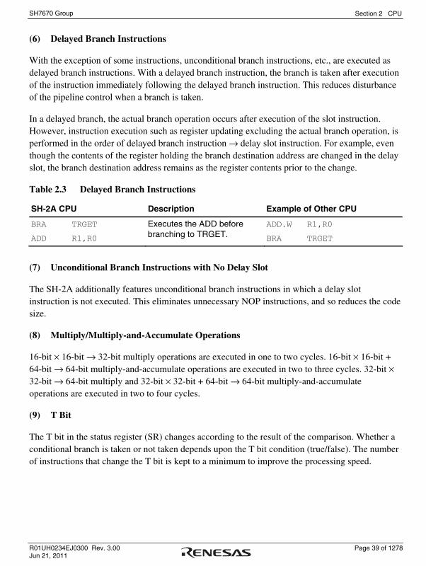
Section 2 CPU
R01UH0234EJ0300 Rev. 3.00 Page 39 of 1278 Jun 21, 2011
SH7670 Group
(6) Delayed Branch Instructions
With the exception of some instructions, unconditional branch instructions, etc., are executed as delayed branch instructions. With a delayed branch instruction, the branch is taken after execution of the instruction immediately following the delayed branch instruction. This reduces disturbance of the pipeline control when a branch is taken.
In a delayed branch, the actual branch operation occurs after execution of the slot instruction. However, instruction execution such as register updating excluding the actual branch operation, is performed in the order of delayed branch instruction → delay slot instruction. For example, even though the contents of the register holding the branch destination address are changed in the delay slot, the branch destination address remains as the register contents prior to the change.
Table 2.3 Delayed Branch Instructions
SH-2A CPU Description Example of Other CPU
BRA TRGET
ADD R1,R0
Executes the ADD before branching to TRGET.
ADD.W R1,R0
BRA TRGET
(7) Unconditional Branch Instructions with No Delay Slot
The SH-2A additionally features unconditional branch instructions in which a delay slot instruction is not executed. This eliminates unnecessary NOP instructions, and so reduces the code size.
(8) Multiply/Multiply-and-Accumulate Operations
16-bit × 16-bit → 32-bit multiply operations are executed in one to two cycles. 16-bit × 16-bit + 64-bit → 64-bit multiply-and-accumulate operations are executed in two to three cycles. 32-bit × 32-bit → 64-bit multiply and 32-bit × 32-bit + 64-bit → 64-bit multiply-and-accumulate operations are executed in two to four cycles.
(9) T Bit
The T bit in the status register (SR) changes according to the result of the comparison. Whether a conditional branch is taken or not taken depends upon the T bit condition (true/false). The number of instructions that change the T bit is kept to a minimum to improve the processing speed.

Section 2 CPU
Page 40 of 1278 R01UH0234EJ0300 Rev. 3.00 Jun 21, 2011
SH7670 Group
Table 2.4 T Bit
SH-2A CPU Description Example of Other CPU
CMP/GE R1,R0
BT TRGET0
BF TRGET1
T bit is set when R0 ≥ R1.
The program branches to TRGET0 when R0 ≥ R1 and to TRGET1 when R0 < R1.
CMP.W R1,R0
BGE TRGET0
BLT TRGET1
ADD #−1,R0
CMP/EQ #0,R0
BT TRGET
T bit is not changed by ADD.
T bit is set when R0 = 0.
The program branches if R0 = 0.
SUB.W #1,R0
BEQ TRGET
(10) Immediate Data
Byte immediate data is located in an instruction code. Word or longword immediate data is not located in instruction codes but in a memory table. The memory table is accessed by an immediate data transfer instruction (MOV) using the PC relative addressing mode with displacement.
With the SH-2A, 17- to 28-bit immediate data can be located in an instruction code. However, for 21- to 28-bit immediate data, an OR instruction must be executed after the data is transferred to a register.
Table 2.5 Immediate Data Accessing
Classification SH-2A CPU Example of Other CPU
8-bit immediate MOV #H'12,R0 MOV.B #H'12,R0
16-bit immediate MOVI20 #H'1234,R0 MOV.W #H'1234,R0
20-bit immediate MOVI20 #H'12345,R0 MOV.L #H'12345,R0
28-bit immediate MOVI20S #H'12345,R0
OR #H'67,R0
MOV.L #H'1234567,R0
32-bit immediate MOV.L @(disp,PC),R0
.................
.DATA.L H'12345678
MOV.L #H'12345678,R0
Note: @(disp, PC) accesses the immediate data.

Section 2 CPU
R01UH0234EJ0300 Rev. 3.00 Page 41 of 1278 Jun 21, 2011
SH7670 Group
(11) Absolute Address
When data is accessed by an absolute address, the absolute address value should be placed in the memory table in advance. That value is transferred to the register by loading the immediate data during the execution of the instruction, and the data is accessed in register indirect addressing mode.
With the SH-2A, when data is referenced using an absolute address not exceeding 28 bits, it is also possible to transfer immediate data located in the instruction code to a register and to reference the data in register indirect addressing mode. However, when referencing data using an absolute address of 21 to 28 bits, an OR instruction must be used after the data is transferred to a register.
Table 2.6 Absolute Address Accessing
Classification SH-2A CPU Example of Other CPU
Up to 20 bits MOVI20 #H'12345,R1
MOV.B @R1,R0
MOV.B @H'12345,R0
21 to 28 bits MOVI20S #H'12345,R1
OR #H'67,R1
MOV.B @R1,R0
MOV.B @H'1234567,R0
29 bits or more MOV.L @(disp,PC),R1
MOV.B @R1,R0
..................
.DATA.L H'12345678
MOV.B @H'12345678,R0
(12) 16-Bit/32-Bit Displacement
When data is accessed by 16-bit or 32-bit displacement, the displacement value should be placed in the memory table in advance. That value is transferred to the register by loading the immediate data during the execution of the instruction, and the data is accessed in the indexed indirect register addressing mode.
Table 2.7 Displacement Accessing
Classification SH-2A CPU Example of Other CPU
16-bit displacement MOV.W @(disp,PC),R0
MOV.W @(R0,R1),R2
..................
.DATA.W H'1234
MOV.W @(H'1234,R1),R2
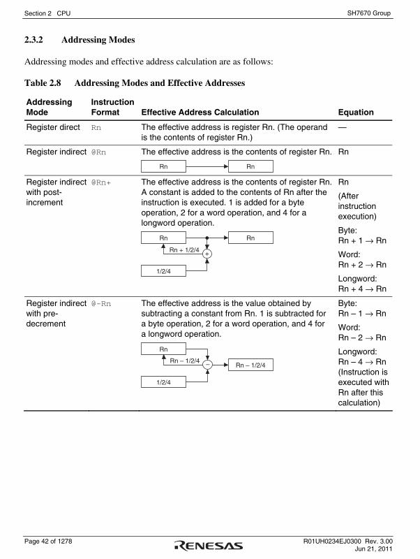
Section 2 CPU
Page 42 of 1278 R01UH0234EJ0300 Rev. 3.00 Jun 21, 2011
SH7670 Group
2.3.2 Addressing Modes
Addressing modes and effective address calculation are as follows:
Table 2.8 Addressing Modes and Effective Addresses
Addressing Mode
Instruction Format
Effective Address Calculation
Equation
Register direct Rn The effective address is register Rn. (The operand is the contents of register Rn.)
—
Register indirect @Rn The effective address is the contents of register Rn.
Rn Rn
Rn
Register indirect with post-increment
@Rn+ The effective address is the contents of register Rn. A constant is added to the contents of Rn after the instruction is executed. 1 is added for a byte operation, 2 for a word operation, and 4 for a longword operation.
Rn Rn
1/2/4
+Rn + 1/2/4
Rn
(After instruction execution)
Byte: Rn + 1 → Rn
Word: Rn + 2 → Rn
Longword: Rn + 4 → Rn
Register indirect with pre-decrement
@-Rn The effective address is the value obtained by subtracting a constant from Rn. 1 is subtracted for a byte operation, 2 for a word operation, and 4 for a longword operation.
Rn
1/2/4
Rn – 1/2/4–Rn – 1/2/4
Byte: Rn – 1 → Rn
Word: Rn – 2 → Rn
Longword: Rn – 4 → Rn (Instruction is executed with Rn after this calculation)

Section 2 CPU
R01UH0234EJ0300 Rev. 3.00 Page 43 of 1278 Jun 21, 2011
SH7670 Group
Addressing Mode
Instruction Format
Effective Address Calculation
Equation
Register indirect with displacement
@(disp:4, Rn)
The effective address is the sum of Rn and a 4-bit displacement (disp). The value of disp is zero-extended, and remains unchanged for a byte operation, is doubled for a word operation, and is quadrupled for a longword operation.
Rn
Rn + disp × 1/2/4+
×
1/2/4
disp(zero-extended)
Byte: Rn + disp
Word: Rn + disp × 2
Longword: Rn + disp × 4
Register indirect with displacement
@(disp:12,Rn)
The effective address is the sum of Rn and a 12-bit displacement (disp). The value of disp is zero-extended.
+
Rn
disp(zero-extended)
Rn + disp
Byte: Rn + disp
Word: Rn + disp
Longword: Rn + disp
Indexed register indirect
@(R0,Rn) The effective address is the sum of Rn and R0.
Rn
R0
Rn + R0+
Rn + R0
GBR indirect with displacement
@(disp:8, GBR)
The effective address is the sum of GBR value and an 8-bit displacement (disp). The value of disp is zero-extended, and remains unchanged for a byte operation, is doubled for a word operation, and is quadrupled for a longword operation.
GBR
1/2/4
GBR+ disp × 1/2/4
+
×
disp(zero-extended)
Byte: GBR + disp
Word: GBR + disp × 2
Longword: GBR + disp × 4

Section 2 CPU
Page 44 of 1278 R01UH0234EJ0300 Rev. 3.00 Jun 21, 2011
SH7670 Group
Addressing Mode
Instruction Format
Effective Address Calculation
Equation
Indexed GBR indirect
@(R0, GBR) The effective address is the sum of GBR value and R0.
GBR
R0
GBR + R0+
GBR + R0
TBR duplicate indirect with displacement
@@ (disp:8, TBR)
The effective address is the sum of TBR value and an 8-bit displacement (disp). The value of disp is zero-extended, and is multiplied by 4.
TBR
TBR
+ disp × 4
(TBR
+ disp × 4)4
+disp(zero-extended)
×
Contents of address (TBR + disp × 4)
PC indirect with displacement
@(disp:8, PC)
The effective address is the sum of PC value and an 8-bit displacement (disp). The value of disp is zero-extended, and is doubled for a word operation, and quadrupled for a longword operation. For a longword operation, the lowest two bits of the PC value are masked.
PC
H'FFFFFFFCPC + disp × 2
orPC & H'FFFFFFFC
+ disp × 4
+
2/4
×
&(for longword)
disp(zero-extended)
Word: PC + disp × 2
Longword: PC & H'FFFFFFFC + disp × 4

Section 2 CPU
R01UH0234EJ0300 Rev. 3.00 Page 45 of 1278 Jun 21, 2011
SH7670 Group
Addressing Mode
Instruction Format
Effective Address Calculation
Equation
PC relative disp:8 The effective address is the sum of PC value and the value that is obtained by doubling the sign-extended 8-bit displacement (disp).
PC
2
+
×
disp(sign-extended)
PC + disp × 2
PC + disp × 2
disp:12 The effective address is the sum of PC value and the value that is obtained by doubling the sign-extended 12-bit displacement (disp).
PC
2
+
×
disp(sign-extended)
PC + disp × 2
PC + disp × 2
Rn The effective address is the sum of PC value and Rn.
PC
Rn
PC + Rn+
PC + Rn

Section 2 CPU
Page 46 of 1278 R01UH0234EJ0300 Rev. 3.00 Jun 21, 2011
SH7670 Group
Addressing Mode
Instruction Format
Effective Address Calculation
Equation
The 20-bit immediate data (imm) for the MOVI20 instruction is sign-extended.
Sign-extended imm (20 bits)
31 19 0
— Immediate #imm:20
The 20-bit immediate data (imm) for the MOVI20S instruction is shifted by eight bits to the left, the upper bits are sign-extended, and the lower bits are padded with zero.
Sign-extended
imm (20 bits) 00000000
31 27 8 0
—
#imm:8 The 8-bit immediate data (imm) for the TST, AND, OR, and XOR instructions is zero-extended.
—
#imm:8 The 8-bit immediate data (imm) for the MOV, ADD, and CMP/EQ instructions is sign-extended.
—
#imm:8 The 8-bit immediate data (imm) for the TRAPA instruction is zero-extended and then quadrupled.
—
#imm:3 The 3-bit immediate data (imm) for the BAND, BOR, BXOR, BST, BLD, BSET, and BCLR instructions indicates the target bit location.
—

Section 2 CPU
R01UH0234EJ0300 Rev. 3.00 Page 47 of 1278 Jun 21, 2011
SH7670 Group
2.3.3 Instruction Format
The instruction formats and the meaning of source and destination operands are described below. The meaning of the operand depends on the instruction code. The symbols used are as follows:
• xxxx: Instruction code
• mmmm: Source register
• nnnn: Destination register
• iiii: Immediate data
• dddd: Displacement Table 2.9 Instruction Formats
Instruction Formats
Source Operand
Destination Operand
Example
0 format
xxxx xxxx xxxxxxxx
15 0
— — NOP
— nnnn: Register direct
MOVT Rn
Control register or system register
nnnn: Register direct
STS MACH,Rn
R0 (Register direct) nnnn: Register direct
DIVU R0,Rn
Control register or system register
nnnn: Register indirect with pre-decrement
STC.L SR,@-Rn
mmmm: Register direct
R15 (Register indirect with pre-decrement)
MOVMU.L Rm,@-R15
R15 (Register indirect with post-increment)
nnnn: Register direct
MOVMU.L @R15+,Rn
n format
xxxx xxxx xxxxnnnn
15 0
R0 (Register direct) nnnn: (Register indirect with post-increment)
MOV.L R0,@Rn+
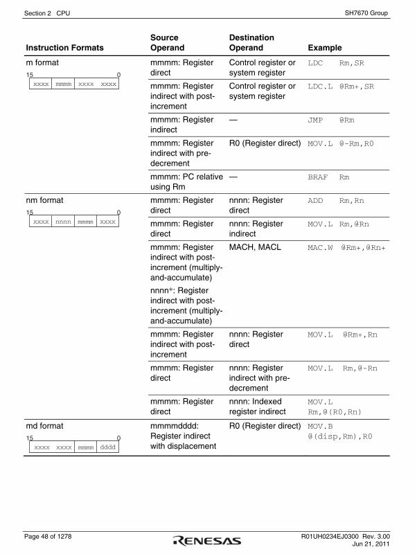
Section 2 CPU
Page 48 of 1278 R01UH0234EJ0300 Rev. 3.00 Jun 21, 2011
SH7670 Group
Instruction Formats
Source Operand
Destination Operand
Example
mmmm: Register direct
Control register or system register
LDC Rm,SR
mmmm: Register indirect with post-increment
Control register or system register
LDC.L @Rm+,SR
mmmm: Register indirect
— JMP @Rm
mmmm: Register indirect with pre-decrement
R0 (Register direct) MOV.L @-Rm,R0
m format
xxxxmmmmxxxx xxxx
15 0
mmmm: PC relative using Rm
— BRAF Rm
mmmm: Register direct
nnnn: Register direct
ADD Rm,Rn
mmmm: Register direct
nnnn: Register indirect
MOV.L Rm,@Rn
mmmm: Register indirect with post-increment (multiply-and-accumulate)
nnnn*: Register indirect with post-increment (multiply-and-accumulate)
MACH, MACL MAC.W @Rm+,@Rn+
mmmm: Register indirect with post-increment
nnnn: Register direct
MOV.L @Rm+,Rn
mmmm: Register direct
nnnn: Register indirect with pre-decrement
MOV.L Rm,@-Rn
nm format
nnnnxxxx xxxx
15 0mmmm
mmmm: Register direct
nnnn: Indexed register indirect
MOV.L Rm,@(R0,Rn)
md format
xxxx dddd
15 0mmmmxxxx
mmmmdddd: Register indirect with displacement
R0 (Register direct) MOV.B @(disp,Rm),R0

Section 2 CPU
R01UH0234EJ0300 Rev. 3.00 Page 49 of 1278 Jun 21, 2011
SH7670 Group
Instruction Formats
Source Operand
Destination Operand
Example
nd4 format
xxxxxxxx dddd
15 0nnnn
R0 (Register direct) nnnndddd: Register indirect with displacement
MOV.B R0,@(disp,Rn)
mmmm: Register direct
nnnndddd: Register indirect with displacement
MOV.L Rm,@(disp,Rn)
nmd format
nnnnxxxx dddd
15 0mmmm
mmmmdddd: Register indirect with displacement
nnnn: Register direct
MOV.L @(disp,Rm),Rn
mmmm: Register direct
nnnndddd: Register indirect with displacement
MOV.L Rm,@(disp12,Rn)
nmd12 format
xxxx dddd dddddddd
15 0
xxxx mmmm xxxxnnnn
32 16
mmmmdddd: Register indirect with displacement
nnnn: Register direct
MOV.L @(disp12,Rm),Rn
dddddddd: GBR indirect with displacement
R0 (Register direct) MOV.L @(disp,GBR),R0
R0 (Register direct) dddddddd: GBR indirect with displacement
MOV.L R0,@(disp,GBR)
dddddddd: PC relative with displacement
R0 (Register direct) MOVA @(disp,PC),R0
dddddddd: TBR duplicate indirect with displacement
— JSR/N @@(disp8,TBR)
d format
ddddxxxx
15 0xxxx dddd
dddddddd: PC relative
— BF label
d12 format
ddddxxxx
15 0dddd dddd
dddddddddddd: PC relative
— BRA label
(label = disp + PC)
nd8 format
ddddnnnnxxxx
15 0dddd
dddddddd: PC relative with displacement
nnnn: Register direct
MOV.L @(disp,PC),Rn
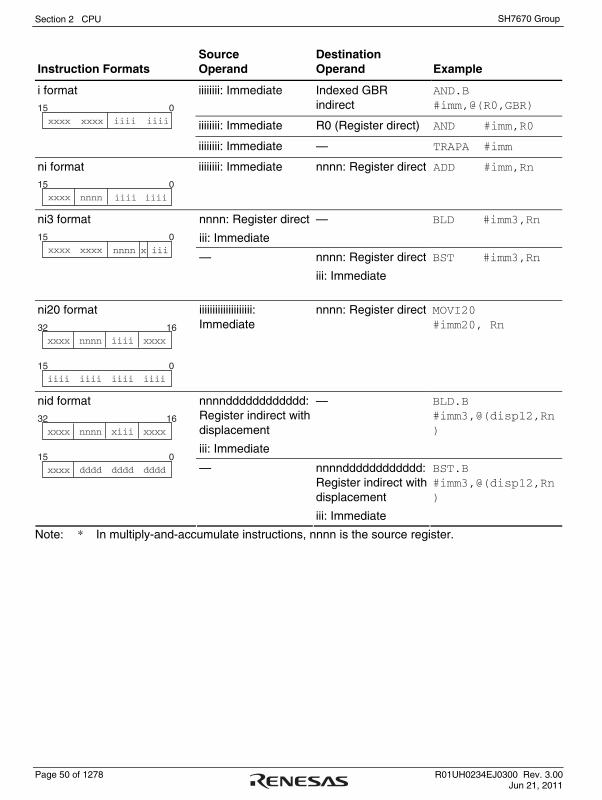
Section 2 CPU
Page 50 of 1278 R01UH0234EJ0300 Rev. 3.00 Jun 21, 2011
SH7670 Group
Instruction Formats
Source Operand
Destination Operand
Example
iiiiiiii: Immediate Indexed GBR indirect
AND.B #imm,@(R0,GBR)
iiiiiiii: Immediate R0 (Register direct) AND #imm,R0
i format
xxxxxxxx iiii
15 0iiii
iiiiiiii: Immediate — TRAPA #imm
ni format
nnnn iiiixxxx
15 0iiii
iiiiiiii: Immediate nnnn: Register direct ADD #imm,Rn
nnnn: Register direct
iii: Immediate
— BLD #imm3,Rn ni3 format
xxxx nnnnxxxx
15 0iiix — nnnn: Register direct
iii: Immediate
BST #imm3,Rn
ni20 format
iiii iiii iiiiiiii
15 0
xxxx iiii xxxxnnnn
32 16
iiiiiiiiiiiiiiiiiiii: Immediate
nnnn: Register direct MOVI20 #imm20, Rn
nnnndddddddddddd: Register indirect with displacement
iii: Immediate
— BLD.B #imm3,@(disp12,Rn)
nid format
xxxx dddd dddddddd
15 0
xxxx xiii xxxxnnnn
32 16
— nnnndddddddddddd: Register indirect with displacement
iii: Immediate
BST.B #imm3,@(disp12,Rn)
Note: * In multiply-and-accumulate instructions, nnnn is the source register.

Section 2 CPU
R01UH0234EJ0300 Rev. 3.00 Page 51 of 1278 Jun 21, 2011
SH7670 Group
2.4 Instruction Set
2.4.1 Instruction Set by Classification
Table 2.10 lists the instructions according to their classification.
Table 2.10 Classification of Instructions
Classification
Types
Operation Code
Function
No. of Instructions
MOV Data transfer
Immediate data transfer
Peripheral module data transfer
Structure data transfer
Reverse stack transfer
MOVA Effective address transfer
MOVI20 20-bit immediate data transfer
MOVI20S 20-bit immediate data transfer
8-bit left-shit
MOVML R0–Rn register save/restore
MOVMU Rn–R14 and PR register save/restore
MOVRT T bit inversion and transfer to Rn
MOVT T bit transfer
MOVU Unsigned data transfer
NOTT T bit inversion
PREF Prefetch to operand cache
SWAP Swap of upper and lower bytes
Data transfer 13
XTRCT Extraction of the middle of registers connected
62
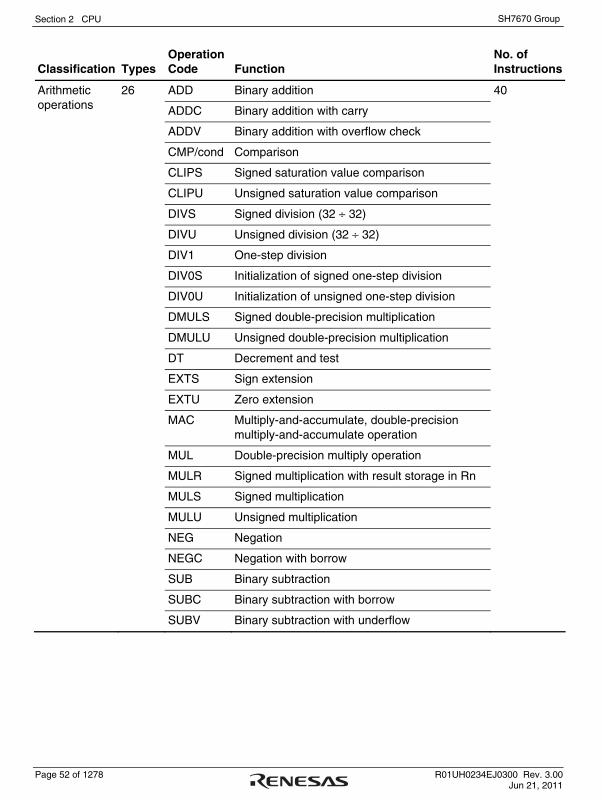
Section 2 CPU
Page 52 of 1278 R01UH0234EJ0300 Rev. 3.00 Jun 21, 2011
SH7670 Group
Classification
Types
Operation Code
Function
No. of Instructions
26 ADD Binary addition 40
ADDC Binary addition with carry
ADDV Binary addition with overflow check
CMP/cond Comparison
CLIPS Signed saturation value comparison
CLIPU Unsigned saturation value comparison
DIVS Signed division (32 ÷ 32)
DIVU Unsigned division (32 ÷ 32)
DIV1 One-step division
Arithmetic operations
DIV0S Initialization of signed one-step division
DIV0U Initialization of unsigned one-step division
DMULS Signed double-precision multiplication
DMULU Unsigned double-precision multiplication
DT Decrement and test
EXTS Sign extension
EXTU Zero extension
MAC Multiply-and-accumulate, double-precision multiply-and-accumulate operation
MUL Double-precision multiply operation
MULR Signed multiplication with result storage in Rn
MULS Signed multiplication
MULU Unsigned multiplication
NEG Negation
NEGC Negation with borrow
SUB Binary subtraction
SUBC Binary subtraction with borrow
SUBV Binary subtraction with underflow

Section 2 CPU
R01UH0234EJ0300 Rev. 3.00 Page 53 of 1278 Jun 21, 2011
SH7670 Group
Classification
Types
Operation Code
Function
No. of Instructions
6 AND Logical AND 14
NOT Bit inversion
OR Logical OR
TAS Memory test and bit set
TST Logical AND and T bit set
Logic operations
XOR Exclusive OR
Shift 12 ROTL One-bit left rotation 16
ROTR One-bit right rotation
ROTCL One-bit left rotation with T bit
ROTCR One-bit right rotation with T bit
SHAD Dynamic arithmetic shift
SHAL One-bit arithmetic left shift
SHAR One-bit arithmetic right shift
SHLD Dynamic logical shift
SHLL One-bit logical left shift
SHLLn n-bit logical left shift
SHLR One-bit logical right shift
SHLRn n-bit logical right shift
Branch 10 BF Conditional branch, conditional delayed branch (branch when T = 0)
15
BT Conditional branch, conditional delayed branch (branch when T = 1)
BRA Unconditional delayed branch
BRAF Unconditional delayed branch
BSR Delayed branch to subroutine procedure
BSRF Delayed branch to subroutine procedure
JMP Unconditional delayed branch
JSR Branch to subroutine procedure
Delayed branch to subroutine procedure
RTS Return from subroutine procedure
Delayed return from subroutine procedure
RTV/N Return from subroutine procedure with Rm → R0 transfer

Section 2 CPU
Page 54 of 1278 R01UH0234EJ0300 Rev. 3.00 Jun 21, 2011
SH7670 Group
Classification
Types
Operation Code
Function
No. of Instructions
14 CLRT T bit clear 36
CLRMAC MAC register clear
System control
LDBANK Register restoration from specified register bank entry
LDC Load to control register
LDS Load to system register
NOP No operation
RESBANK Register restoration from register bank
RTE Return from exception handling
SETT T bit set
SLEEP Transition to power-down mode
STBANK Register save to specified register bank entry
STC Store control register data
STS Store system register data
TRAPA Trap exception handling
19 FABS Floating-point absolute value 48 Floating-point instructions FADD Floating-point addition
FCMP Floating-point comparison
FCNVDS Conversion from double-precision to single-precision
FCNVSD Conversion from single-precision to double -precision
FDIV Floating-point division
FLDI0 Floating-point load immediate 0
FLDI1 Floating-point load immediate 1
FLDS Floating-point load into system register FPUL
FLOAT Conversion from integer to floating-point
FMAC Floating-point multiply and accumulate operation
FMOV Floating-point data transfer
FMUL Floating-point multiplication
FNEG Floating-point sign inversion

Section 2 CPU
R01UH0234EJ0300 Rev. 3.00 Page 55 of 1278 Jun 21, 2011
SH7670 Group
Classification
Types
Operation Code
Function
No. of Instructions
19 FSCHG SZ bit inversion 48 Floating-point instructions FSQRT Floating-point square root
FSTS Floating-point store from system register FPUL
FSUB Floating-point subtraction
FTRC Floating-point conversion with rounding to integer
LDS Load into floating-point system register FPU-related CPU instructions
2
STS Store from floating-point system register
8
10 BAND Bit AND 14 Bit manipulation BCLR Bit clear
BLD Bit load
BOR Bit OR
BSET Bit set
BST Bit store
BXOR Bit exclusive OR
BANDNOT Bit NOT AND
BORNOT Bit NOT OR
BLDNOT Bit NOT load
Total: 112 253

Section 2 CPU
Page 56 of 1278 R01UH0234EJ0300 Rev. 3.00 Jun 21, 2011
SH7670 Group
The table below shows the format of instruction codes, operation, and execution states. They are described by using this format according to their classification.
Instruction Instruction Code Operation Execution States T Bit
Indicated by mnemonic.
[Legend]
Rm: Source register
Rn: Destination register
imm: Immediate data
disp: Displacement*2
Indicated in MSB ↔ LSB order.
[Legend]
mmmm: Source register
nnnn: Destination register 0000: R0 0001: R1 ......... 1111: R15
iiii: Immediate data
dddd: Displacement
Indicates summary of operation.
[Legend]
→, ←: Transfer direction
(xx): Memory operand
M/Q/T: Flag bits in SR
&: Logical AND of each bit
|: Logical OR of each bit
^: Exclusive logical OR of each bit
~: Logical NOT of each bit
<<n: n-bit left shift
>>n: n-bit right shift
Value when no wait states are inserted.*1
Value of T bit after instruction is executed.
Explanation of Symbols
—: No change
Notes: 1. Instruction execution cycles: The execution cycles shown in the table are minimums. In practice, the number of instruction execution states will be increased in cases such as the following:
a. When there is a conflict between an instruction fetch and a data access b. When the destination register of a load instruction (memory → register) is the same
as the register used by the next instruction. 2. Depending on the operand size, displacement is scaled by ×1, ×2, or ×4. For details,
refer to the SH-2A, SH2A-FPU Software Manual.
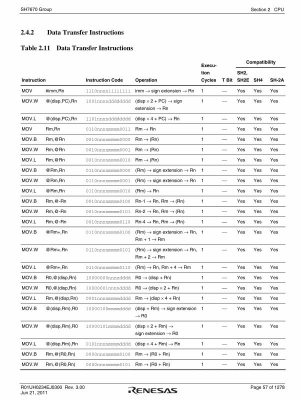
Section 2 CPU
R01UH0234EJ0300 Rev. 3.00 Page 57 of 1278 Jun 21, 2011
SH7670 Group
2.4.2 Data Transfer Instructions
Table 2.11 Data Transfer Instructions
Compatibility
Instruction Instruction Code Operation
Execu-
tion
Cycles T Bit
SH2,
SH2E SH4 SH-2A
MOV #imm,Rn 1110nnnniiiiiiii imm → sign extension → Rn 1 ⎯ Yes Yes Yes
MOV.W @(disp,PC),Rn 1001nnnndddddddd (disp × 2 + PC) → sign
extension → Rn
1 ⎯ Yes Yes Yes
MOV.L @(disp,PC),Rn 1101nnnndddddddd (disp × 4 + PC) → Rn 1 ⎯ Yes Yes Yes
MOV Rm,Rn 0110nnnnmmmm0011 Rm → Rn 1 ⎯ Yes Yes Yes
MOV.B Rm,@Rn 0010nnnnmmmm0000 Rm → (Rn) 1 ⎯ Yes Yes Yes
MOV.W Rm,@Rn 0010nnnnmmmm0001 Rm → (Rn) 1 ⎯ Yes Yes Yes
MOV.L Rm,@Rn 0010nnnnmmmm0010 Rm → (Rn) 1 ⎯ Yes Yes Yes
MOV.B @Rm,Rn 0110nnnnmmmm0000 (Rm) → sign extension → Rn 1 ⎯ Yes Yes Yes
MOV.W @Rm,Rn 0110nnnnmmmm0001 (Rm) → sign extension → Rn 1 ⎯ Yes Yes Yes
MOV.L @Rm,Rn 0110nnnnmmmm0010 (Rm) → Rn 1 ⎯ Yes Yes Yes
MOV.B Rm,@-Rn 0010nnnnmmmm0100 Rn-1 → Rn, Rm → (Rn) 1 ⎯ Yes Yes Yes
MOV.W Rm,@-Rn 0010nnnnmmmm0101 Rn-2 → Rn, Rm → (Rn) 1 ⎯ Yes Yes Yes
MOV.L Rm,@-Rn 0010nnnnmmmm0110 Rn-4 → Rn, Rm → (Rn) 1 ⎯ Yes Yes Yes
MOV.B @Rm+,Rn 0110nnnnmmmm0100 (Rm) → sign extension → Rn,
Rm + 1 → Rm
1 ⎯ Yes Yes Yes
MOV.W @Rm+,Rn 0110nnnnmmmm0101 (Rm) → sign extension → Rn,
Rm + 2 → Rm
1 ⎯ Yes Yes Yes
MOV.L @Rm+,Rn 0110nnnnmmmm0110 (Rm) → Rn, Rm + 4 → Rm 1 ⎯ Yes Yes Yes
MOV.B R0,@(disp,Rn) 10000000nnnndddd R0 → (disp + Rn) 1 ⎯ Yes Yes Yes
MOV.W R0,@(disp,Rn) 10000001nnnndddd R0 → (disp × 2 + Rn) 1 ⎯ Yes Yes Yes
MOV.L Rm,@(disp,Rn) 0001nnnnmmmmdddd Rm → (disp × 4 + Rn) 1 ⎯ Yes Yes Yes
MOV.B @(disp,Rm),R0 10000100mmmmdddd (disp + Rm) → sign extension
→ R0
1 ⎯ Yes Yes Yes
MOV.W @(disp,Rm),R0 10000101mmmmdddd (disp × 2 + Rm) →
sign extension → R0
1 ⎯ Yes Yes Yes
MOV.L @(disp,Rm),Rn 0101nnnnmmmmdddd (disp × 4 + Rm) → Rn 1 ⎯ Yes Yes Yes
MOV.B Rm,@(R0,Rn) 0000nnnnmmmm0100 Rm → (R0 + Rn) 1 ⎯ Yes Yes Yes
MOV.W Rm,@(R0,Rn) 0000nnnnmmmm0101 Rm → (R0 + Rn) 1 ⎯ Yes Yes Yes
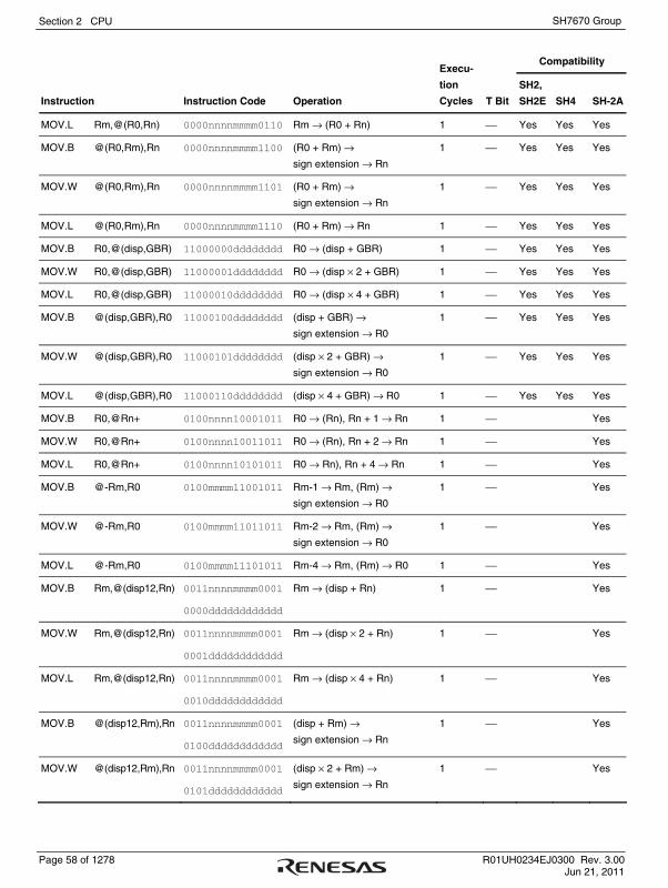
Section 2 CPU
Page 58 of 1278 R01UH0234EJ0300 Rev. 3.00 Jun 21, 2011
SH7670 Group
Compatibility
Instruction Instruction Code Operation
Execu-
tion
Cycles T Bit
SH2,
SH2E SH4 SH-2A
MOV.L Rm,@(R0,Rn) 0000nnnnmmmm0110 Rm → (R0 + Rn) 1 ⎯ Yes Yes Yes
MOV.B @(R0,Rm),Rn 0000nnnnmmmm1100 (R0 + Rm) →
sign extension → Rn
1 ⎯ Yes Yes Yes
MOV.W @(R0,Rm),Rn 0000nnnnmmmm1101 (R0 + Rm) →
sign extension → Rn
1 ⎯ Yes Yes Yes
MOV.L @(R0,Rm),Rn 0000nnnnmmmm1110 (R0 + Rm) → Rn 1 ⎯ Yes Yes Yes
MOV.B R0,@(disp,GBR) 11000000dddddddd R0 → (disp + GBR) 1 ⎯ Yes Yes Yes
MOV.W R0,@(disp,GBR) 11000001dddddddd R0 → (disp × 2 + GBR) 1 ⎯ Yes Yes Yes
MOV.L R0,@(disp,GBR) 11000010dddddddd R0 → (disp × 4 + GBR) 1 ⎯ Yes Yes Yes
MOV.B @(disp,GBR),R0 11000100dddddddd (disp + GBR) →
sign extension → R0
1 ⎯ Yes Yes Yes
MOV.W @(disp,GBR),R0 11000101dddddddd (disp × 2 + GBR) →
sign extension → R0
1 ⎯ Yes Yes Yes
MOV.L @(disp,GBR),R0 11000110dddddddd (disp × 4 + GBR) → R0 1 ⎯ Yes Yes Yes
MOV.B R0,@Rn+ 0100nnnn10001011 R0 → (Rn), Rn + 1 → Rn 1 ⎯ Yes
MOV.W R0,@Rn+ 0100nnnn10011011 R0 → (Rn), Rn + 2 → Rn 1 ⎯ Yes
MOV.L R0,@Rn+ 0100nnnn10101011 R0 → Rn), Rn + 4 → Rn 1 ⎯ Yes
MOV.B @-Rm,R0 0100mmmm11001011 Rm-1 → Rm, (Rm) →
sign extension → R0
1 ⎯ Yes
MOV.W @-Rm,R0 0100mmmm11011011 Rm-2 → Rm, (Rm) →
sign extension → R0
1 ⎯ Yes
MOV.L @-Rm,R0 0100mmmm11101011 Rm-4 → Rm, (Rm) → R0 1 ⎯ Yes
MOV.B Rm,@(disp12,Rn) 0011nnnnmmmm0001
0000dddddddddddd
Rm → (disp + Rn) 1 ⎯ Yes
MOV.W Rm,@(disp12,Rn) 0011nnnnmmmm0001
0001dddddddddddd
Rm → (disp × 2 + Rn) 1 ⎯ Yes
MOV.L Rm,@(disp12,Rn) 0011nnnnmmmm0001
0010dddddddddddd
Rm → (disp × 4 + Rn) 1 ⎯ Yes
MOV.B @(disp12,Rm),Rn 0011nnnnmmmm0001
0100dddddddddddd
(disp + Rm) →
sign extension → Rn
1 ⎯ Yes
MOV.W @(disp12,Rm),Rn 0011nnnnmmmm0001
0101dddddddddddd
(disp × 2 + Rm) →
sign extension → Rn
1 ⎯ Yes
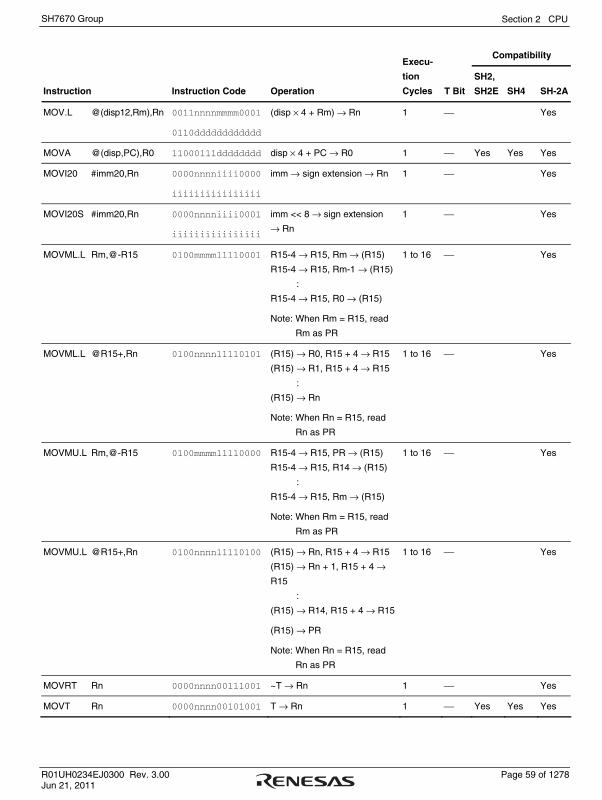
Section 2 CPU
R01UH0234EJ0300 Rev. 3.00 Page 59 of 1278 Jun 21, 2011
SH7670 Group
Compatibility
Instruction Instruction Code Operation
Execu-
tion
Cycles T Bit
SH2,
SH2E SH4 SH-2A
MOV.L @(disp12,Rm),Rn 0011nnnnmmmm0001
0110dddddddddddd
(disp × 4 + Rm) → Rn 1 ⎯ Yes
MOVA @(disp,PC),R0 11000111dddddddd disp × 4 + PC → R0 1 ⎯ Yes Yes Yes
MOVI20 #imm20,Rn 0000nnnniiii0000
iiiiiiiiiiiiiiii
imm → sign extension → Rn 1 ⎯ Yes
MOVI20S #imm20,Rn 0000nnnniiii0001
iiiiiiiiiiiiiiii
imm << 8 → sign extension
→ Rn
1 ⎯ Yes
MOVML.L Rm,@-R15 0100mmmm11110001 R15-4 → R15, Rm → (R15)
R15-4 → R15, Rm-1 → (R15)
:
R15-4 → R15, R0 → (R15)
Note: When Rm = R15, read
Rm as PR
1 to 16 ⎯ Yes
MOVML.L @R15+,Rn 0100nnnn11110101 (R15) → R0, R15 + 4 → R15
(R15) → R1, R15 + 4 → R15
:
(R15) → Rn
Note: When Rn = R15, read
Rn as PR
1 to 16 ⎯ Yes
MOVMU.L Rm,@-R15 0100mmmm11110000 R15-4 → R15, PR → (R15)
R15-4 → R15, R14 → (R15)
:
R15-4 → R15, Rm → (R15)
Note: When Rm = R15, read
Rm as PR
1 to 16 ⎯ Yes
MOVMU.L @R15+,Rn 0100nnnn11110100 (R15) → Rn, R15 + 4 → R15
(R15) → Rn + 1, R15 + 4 →
R15
:
(R15) → R14, R15 + 4 → R15
(R15) → PR
Note: When Rn = R15, read
Rn as PR
1 to 16 ⎯ Yes
MOVRT Rn 0000nnnn00111001 ~T → Rn 1 ⎯ Yes
MOVT Rn 0000nnnn00101001 T → Rn 1 ⎯ Yes Yes Yes

Section 2 CPU
Page 60 of 1278 R01UH0234EJ0300 Rev. 3.00 Jun 21, 2011
SH7670 Group
Compatibility
Instruction Instruction Code Operation
Execu-
tion
Cycles T Bit
SH2,
SH2E SH4 SH-2A
MOVU.B @(disp12,Rm),Rn 0011nnnnmmmm0001
1000dddddddddddd
(disp + Rm) →
zero extension → Rn
1
⎯ Yes
MOVU.W @(disp12,Rm),Rn 0011nnnnmmmm0001
1001dddddddddddd
(disp × 2 + Rm) →
zero extension → Rn
1
⎯ Yes
NOTT 0000000001101000 ~T → T 1 Ope-
ration
result
Yes
PREF @Rn 0000nnnn10000011 (Rn) → operand cache 1 ⎯ Yes Yes
SWAP.B Rm,Rn 0110nnnnmmmm1000 Rm → swap lower 2 bytes →
Rn
1 ⎯ Yes Yes Yes
SWAP.W Rm,Rn 0110nnnnmmmm1001 Rm → swap upper and lower
words → Rn
1 ⎯ Yes Yes Yes
XTRCT Rm,Rn 0010nnnnmmmm1101 Middle 32 bits of Rm:Rn → Rn 1 ⎯ Yes Yes Yes

Section 2 CPU
R01UH0234EJ0300 Rev. 3.00 Page 61 of 1278 Jun 21, 2011
SH7670 Group
2.4.3 Arithmetic Operation Instructions
Table 2.12 Arithmetic Operation Instructions
Compatibility
Instruction Instruction Code Operation
Execu-
tion
Cycles T Bit
SH2,
SH2E SH4 SH-2A
ADD Rm,Rn 0011nnnnmmmm1100 Rn + Rm → Rn 1 ⎯ Yes Yes Yes
ADD #imm,Rn 0111nnnniiiiiiii Rn + imm → Rn 1 ⎯ Yes Yes Yes
ADDC Rm,Rn 0011nnnnmmmm1110 Rn + Rm + T → Rn, carry → T 1 Carry Yes Yes Yes
ADDV Rm,Rn 0011nnnnmmmm1111 Rn + Rm → Rn, overflow → T 1 Over-
flow
Yes Yes Yes
CMP/EQ #imm,R0 10001000iiiiiiii When R0 = imm, 1 → T
Otherwise, 0 → T
1 Com-
parison
result
Yes Yes Yes
CMP/EQ Rm,Rn 0011nnnnmmmm0000 When Rn = Rm, 1 → T
Otherwise, 0 → T
1 Com-
parison
result
Yes Yes Yes
CMP/HS Rm,Rn 0011nnnnmmmm0010 When Rn ≥ Rm (unsigned),
1 → T
Otherwise, 0 → T
1 Com-
parison
result
Yes Yes Yes
CMP/GE Rm,Rn 0011nnnnmmmm0011 When Rn ≥ Rm (signed),
1 → T
Otherwise, 0 → T
1 Com-
parison
result
Yes Yes Yes
CMP/HI Rm,Rn 0011nnnnmmmm0110 When Rn > Rm (unsigned),
1 → T
Otherwise, 0 → T
1 Com-
parison
result
Yes Yes Yes
CMP/GT Rm,Rn 0011nnnnmmmm0111 When Rn > Rm (signed),
1 → T
Otherwise, 0 → T
1 Com-
parison
result
Yes Yes Yes
CMP/PL Rn 0100nnnn00010101 When Rn > 0, 1 → T
Otherwise, 0 → T
1 Com-
parison
result
Yes Yes Yes
CMP/PZ Rn 0100nnnn00010001 When Rn ≥ 0, 1 → T
Otherwise, 0 → T
1 Com-
parison
result
Yes Yes Yes
CMP/STR Rm,Rn 0010nnnnmmmm1100 When any bytes are equal,
1 → T
Otherwise, 0 → T
1 Com-
parison
result
Yes Yes Yes

Section 2 CPU
Page 62 of 1278 R01UH0234EJ0300 Rev. 3.00 Jun 21, 2011
SH7670 Group
Compatibility
Instruction Instruction Code Operation
Execu-
tion
Cycles T Bit
SH2,
SH2E SH4 SH-2A
CLIPS.B Rn 0100nnnn10010001 When Rn > (H'0000007F),
(H'0000007F) → Rn, 1 → CS
when Rn < (H'FFFFFF80),
(H'FFFFFF80) → Rn, 1 → CS
1 ⎯ Yes
CLIPS.W Rn 0100nnnn10010101 When Rn > (H'00007FFF),
(H'00007FFF) → Rn, 1 → CS
When Rn < (H'FFFF8000),
(H'FFFF8000) → Rn, 1 → CS
1 ⎯ Yes
CLIPU.B Rn 0100nnnn10000001 When Rn > (H'000000FF),
(H'000000FF) → Rn, 1 → CS
1 ⎯ Yes
CLIPU.W Rn 0100nnnn10000101 When Rn > (H'0000FFFF),
(H'0000FFFF) → Rn, 1 → CS
1 ⎯ Yes
DIV1 Rm,Rn 0011nnnnmmmm0100 1-step division (Rn ÷ Rm) 1 Calcu-
lation
result
Yes Yes Yes
DIV0S Rm,Rn 0010nnnnmmmm0111 MSB of Rn → Q,
MSB of Rm → M, M ^ Q → T
1 Calcu-
lation
result
Yes Yes Yes
DIV0U 0000000000011001 0 → M/Q/T 1 0 Yes Yes Yes
DIVS R0,Rn 0100nnnn10010100 Signed operation of Rn ÷ R0
→ Rn 32 ÷ 32 → 32 bits
36 ⎯ Yes
DIVU R0,Rn 0100nnnn10000100 Unsigned operation of Rn ÷ R0
→ Rn 32 ÷ 32 → 32 bits
34 ⎯ Yes
DMULS.L Rm,Rn 0011nnnnmmmm1101 Signed operation of Rn × Rm
→ MACH, MACL
32 × 32 → 64 bits
2
⎯ Yes Yes Yes
DMULU.L Rm,Rn 0011nnnnmmmm0101 Unsigned operation of Rn ×
Rm → MACH, MACL
32 × 32 → 64 bits
2
⎯ Yes Yes Yes
DT Rn 0100nnnn00010000 Rn – 1 → Rn
When Rn is 0, 1 → T
When Rn is not 0, 0 → T
1 Compa-
rison
result
Yes Yes Yes
EXTS.B Rm,Rn 0110nnnnmmmm1110 Byte in Rm is
sign-extended → Rn
1 ⎯ Yes Yes Yes
EXTS.W Rm,Rn 0110nnnnmmmm1111 Word in Rm is
sign-extended → Rn
1 ⎯ Yes Yes Yes

Section 2 CPU
R01UH0234EJ0300 Rev. 3.00 Page 63 of 1278 Jun 21, 2011
SH7670 Group
Compatibility
Instruction Instruction Code Operation
Execu-
tion
Cycles T Bit
SH2,
SH2E SH4 SH-2A
EXTU.B Rm,Rn 0110nnnnmmmm1100 Byte in Rm is
zero-extended → Rn
1 ⎯ Yes Yes Yes
EXTU.W Rm,Rn 0110nnnnmmmm1101 Word in Rm is
zero-extended → Rn
1 ⎯ Yes Yes Yes
MAC.L @Rm+,@Rn+ 0000nnnnmmmm1111 Signed operation of (Rn) ×
(Rm) + MAC → MAC
32 × 32 + 64 → 64 bits
4 ⎯ Yes Yes Yes
MAC.W @Rm+,@Rn+ 0100nnnnmmmm1111 Signed operation of (Rn) ×
(Rm) + MAC → MAC
16 × 16 + 64 → 64 bits
3
⎯ Yes Yes Yes
MUL.L Rm,Rn 0000nnnnmmmm0111 Rn × Rm → MACL
32 × 32 → 32 bits
2 ⎯ Yes Yes Yes
MULR R0,Rn 0100nnnn10000000 R0 × Rn → Rn
32 × 32 → 32 bits
2 Yes
MULS.W Rm,Rn 0010nnnnmmmm1111 Signed operation of Rn × Rm
→ MACL
16 × 16 → 32 bits
1 ⎯ Yes Yes Yes
MULU.W Rm,Rn 0010nnnnmmmm1110 Unsigned operation of Rn ×
Rm → MACL
16 × 16 → 32 bits
1
⎯ Yes Yes Yes
NEG Rm,Rn 0110nnnnmmmm1011 0-Rm → Rn 1 ⎯ Yes Yes Yes
NEGC Rm,Rn 0110nnnnmmmm1010 0-Rm-T → Rn, borrow → T 1 Borrow Yes Yes Yes
SUB Rm,Rn 0011nnnnmmmm1000 Rn-Rm → Rn 1 ⎯ Yes Yes Yes
SUBC Rm,Rn 0011nnnnmmmm1010 Rn-Rm-T → Rn, borrow → T 1 Borrow Yes Yes Yes
SUBV Rm,Rn 0011nnnnmmmm1011 Rn-Rm → Rn, underflow → T 1 Over-
flow
Yes Yes Yes
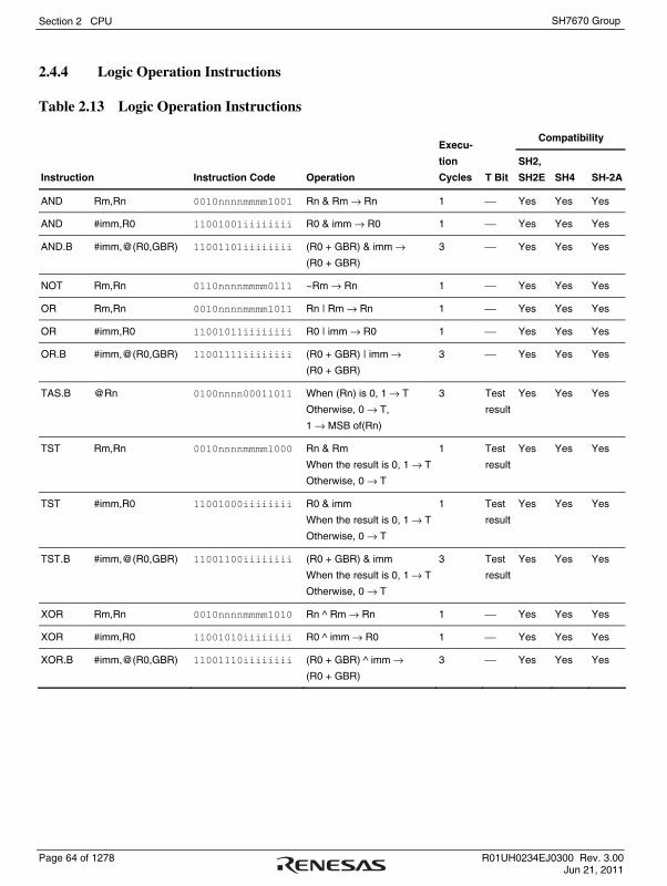
Section 2 CPU
Page 64 of 1278 R01UH0234EJ0300 Rev. 3.00 Jun 21, 2011
SH7670 Group
2.4.4 Logic Operation Instructions
Table 2.13 Logic Operation Instructions
Compatibility
Instruction Instruction Code Operation
Execu-
tion
Cycles T Bit
SH2,
SH2E SH4 SH-2A
AND Rm,Rn 0010nnnnmmmm1001 Rn & Rm → Rn 1 ⎯ Yes Yes Yes
AND #imm,R0 11001001iiiiiiii R0 & imm → R0 1 ⎯ Yes Yes Yes
AND.B #imm,@(R0,GBR) 11001101iiiiiiii (R0 + GBR) & imm →
(R0 + GBR)
3 ⎯ Yes Yes Yes
NOT Rm,Rn 0110nnnnmmmm0111 ~Rm → Rn 1 ⎯ Yes Yes Yes
OR Rm,Rn 0010nnnnmmmm1011 Rn | Rm → Rn 1 ⎯ Yes Yes Yes
OR #imm,R0 11001011iiiiiiii R0 | imm → R0 1 ⎯ Yes Yes Yes
OR.B #imm,@(R0,GBR) 11001111iiiiiiii (R0 + GBR) | imm →
(R0 + GBR)
3 ⎯ Yes Yes Yes
TAS.B @Rn 0100nnnn00011011 When (Rn) is 0, 1 → T
Otherwise, 0 → T,
1 → MSB of(Rn)
3 Test
result
Yes Yes Yes
TST Rm,Rn 0010nnnnmmmm1000 Rn & Rm
When the result is 0, 1 → T
Otherwise, 0 → T
1 Test
result
Yes Yes Yes
TST #imm,R0 11001000iiiiiiii R0 & imm
When the result is 0, 1 → T
Otherwise, 0 → T
1 Test
result
Yes Yes Yes
TST.B #imm,@(R0,GBR) 11001100iiiiiiii (R0 + GBR) & imm
When the result is 0, 1 → T
Otherwise, 0 → T
3 Test
result
Yes Yes Yes
XOR Rm,Rn 0010nnnnmmmm1010 Rn ^ Rm → Rn 1 ⎯ Yes Yes Yes
XOR #imm,R0 11001010iiiiiiii R0 ^ imm → R0 1 ⎯ Yes Yes Yes
XOR.B #imm,@(R0,GBR) 11001110iiiiiiii (R0 + GBR) ^ imm →
(R0 + GBR)
3 ⎯ Yes Yes Yes
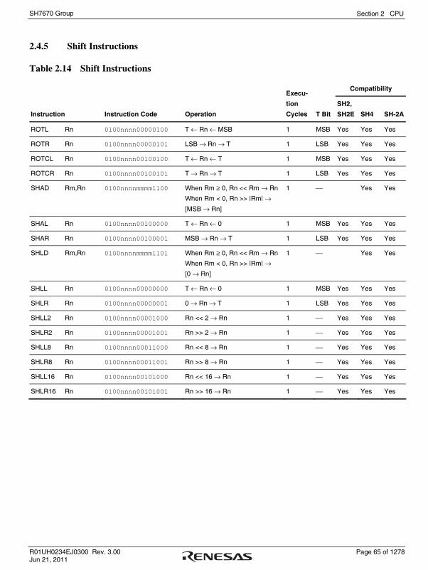
Section 2 CPU
R01UH0234EJ0300 Rev. 3.00 Page 65 of 1278 Jun 21, 2011
SH7670 Group
2.4.5 Shift Instructions
Table 2.14 Shift Instructions
Compatibility
Instruction Instruction Code Operation
Execu-
tion
Cycles T Bit
SH2,
SH2E SH4 SH-2A
ROTL Rn 0100nnnn00000100 T ← Rn ← MSB 1 MSB Yes Yes Yes
ROTR Rn 0100nnnn00000101 LSB → Rn → T 1 LSB Yes Yes Yes
ROTCL Rn 0100nnnn00100100 T ← Rn ← T 1 MSB Yes Yes Yes
ROTCR Rn 0100nnnn00100101 T → Rn → T 1 LSB Yes Yes Yes
SHAD Rm,Rn 0100nnnnmmmm1100 When Rm ≥ 0, Rn << Rm → Rn
When Rm < 0, Rn >> |Rm| →
[MSB → Rn]
1 ⎯ Yes Yes
SHAL Rn 0100nnnn00100000 T ← Rn ← 0 1 MSB Yes Yes Yes
SHAR Rn 0100nnnn00100001 MSB → Rn → T 1 LSB Yes Yes Yes
SHLD Rm,Rn 0100nnnnmmmm1101 When Rm ≥ 0, Rn << Rm → Rn
When Rm < 0, Rn >> |Rm| →
[0 → Rn]
1 ⎯ Yes Yes
SHLL Rn 0100nnnn00000000 T ← Rn ← 0 1 MSB Yes Yes Yes
SHLR Rn 0100nnnn00000001 0 → Rn → T 1 LSB Yes Yes Yes
SHLL2 Rn 0100nnnn00001000 Rn << 2 → Rn 1 ⎯ Yes Yes Yes
SHLR2 Rn 0100nnnn00001001 Rn >> 2 → Rn 1 ⎯ Yes Yes Yes
SHLL8 Rn 0100nnnn00011000 Rn << 8 → Rn 1 ⎯ Yes Yes Yes
SHLR8 Rn 0100nnnn00011001 Rn >> 8 → Rn 1 ⎯ Yes Yes Yes
SHLL16 Rn 0100nnnn00101000 Rn << 16 → Rn 1 ⎯ Yes Yes Yes
SHLR16 Rn 0100nnnn00101001 Rn >> 16 → Rn 1 ⎯ Yes Yes Yes
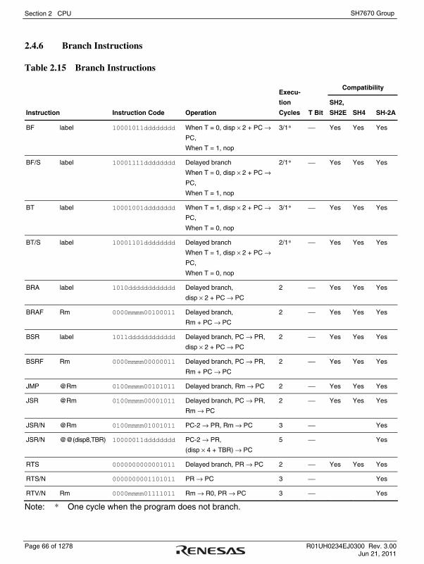
Section 2 CPU
Page 66 of 1278 R01UH0234EJ0300 Rev. 3.00 Jun 21, 2011
SH7670 Group
2.4.6 Branch Instructions
Table 2.15 Branch Instructions
Compatibility
Instruction Instruction Code Operation
Execu-
tion
Cycles T Bit
SH2,
SH2E SH4 SH-2A
BF label 10001011dddddddd When T = 0, disp × 2 + PC →
PC,
When T = 1, nop
3/1* ⎯ Yes Yes Yes
BF/S label 10001111dddddddd Delayed branch
When T = 0, disp × 2 + PC →
PC,
When T = 1, nop
2/1*
⎯ Yes Yes Yes
BT label 10001001dddddddd When T = 1, disp × 2 + PC →
PC,
When T = 0, nop
3/1* ⎯ Yes Yes Yes
BT/S label 10001101dddddddd Delayed branch
When T = 1, disp × 2 + PC →
PC,
When T = 0, nop
2/1* ⎯ Yes Yes Yes
BRA label 1010dddddddddddd Delayed branch,
disp × 2 + PC → PC
2 ⎯ Yes Yes Yes
BRAF Rm 0000mmmm00100011 Delayed branch,
Rm + PC → PC
2 ⎯ Yes Yes Yes
BSR label 1011dddddddddddd Delayed branch, PC → PR,
disp × 2 + PC → PC
2 ⎯ Yes Yes Yes
BSRF Rm 0000mmmm00000011 Delayed branch, PC → PR,
Rm + PC → PC
2 ⎯ Yes Yes Yes
JMP @Rm 0100mmmm00101011 Delayed branch, Rm → PC 2 ⎯ Yes Yes Yes
JSR @Rm 0100mmmm00001011 Delayed branch, PC → PR,
Rm → PC
2 ⎯ Yes Yes Yes
JSR/N @Rm 0100mmmm01001011 PC-2 → PR, Rm → PC 3 ⎯ Yes
JSR/N @@(disp8,TBR) 10000011dddddddd PC-2 → PR,
(disp × 4 + TBR) → PC
5 ⎯ Yes
RTS 0000000000001011 Delayed branch, PR → PC 2 ⎯ Yes Yes Yes
RTS/N 0000000001101011 PR → PC 3 ⎯ Yes
RTV/N Rm 0000mmmm01111011 Rm → R0, PR → PC 3 ⎯ Yes
Note: * One cycle when the program does not branch.
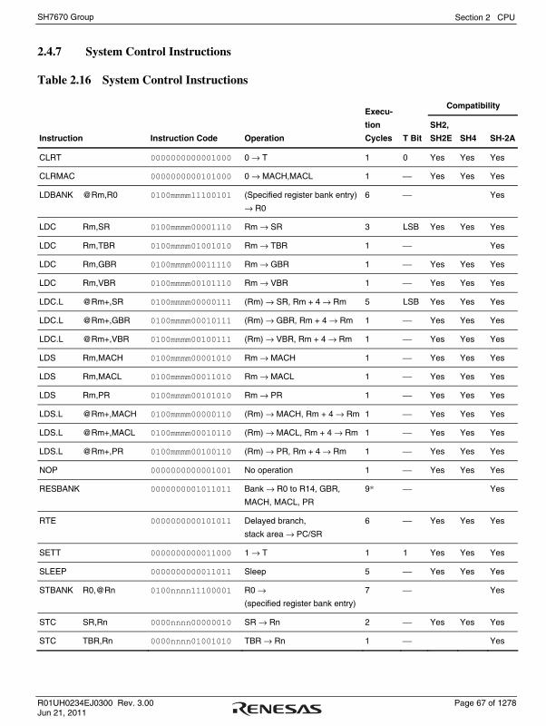
Section 2 CPU
R01UH0234EJ0300 Rev. 3.00 Page 67 of 1278 Jun 21, 2011
SH7670 Group
2.4.7 System Control Instructions
Table 2.16 System Control Instructions
Compatibility
Instruction Instruction Code Operation
Execu-
tion
Cycles T Bit
SH2,
SH2E SH4 SH-2A
CLRT 0000000000001000 0 → T 1 0 Yes Yes Yes
CLRMAC 0000000000101000 0 → MACH,MACL 1 ⎯ Yes Yes Yes
LDBANK @Rm,R0 0100mmmm11100101 (Specified register bank entry)
→ R0
6 ⎯ Yes
LDC Rm,SR 0100mmmm00001110 Rm → SR 3 LSB Yes Yes Yes
LDC Rm,TBR 0100mmmm01001010 Rm → TBR 1 ⎯ Yes
LDC Rm,GBR 0100mmmm00011110 Rm → GBR 1 ⎯ Yes Yes Yes
LDC Rm,VBR 0100mmmm00101110 Rm → VBR 1 ⎯ Yes Yes Yes
LDC.L @Rm+,SR 0100mmmm00000111 (Rm) → SR, Rm + 4 → Rm 5 LSB Yes Yes Yes
LDC.L @Rm+,GBR 0100mmmm00010111 (Rm) → GBR, Rm + 4 → Rm 1 ⎯ Yes Yes Yes
LDC.L @Rm+,VBR 0100mmmm00100111 (Rm) → VBR, Rm + 4 → Rm 1 ⎯ Yes Yes Yes
LDS Rm,MACH 0100mmmm00001010 Rm → MACH 1 ⎯ Yes Yes Yes
LDS Rm,MACL 0100mmmm00011010 Rm → MACL 1 ⎯ Yes Yes Yes
LDS Rm,PR 0100mmmm00101010 Rm → PR 1 ⎯ Yes Yes Yes
LDS.L @Rm+,MACH 0100mmmm00000110 (Rm) → MACH, Rm + 4 → Rm 1 ⎯ Yes Yes Yes
LDS.L @Rm+,MACL 0100mmmm00010110 (Rm) → MACL, Rm + 4 → Rm 1 ⎯ Yes Yes Yes
LDS.L @Rm+,PR 0100mmmm00100110 (Rm) → PR, Rm + 4 → Rm 1 ⎯ Yes Yes Yes
NOP 0000000000001001 No operation 1 ⎯ Yes Yes Yes
RESBANK 0000000001011011 Bank → R0 to R14, GBR,
MACH, MACL, PR
9* ⎯ Yes
RTE 0000000000101011 Delayed branch,
stack area → PC/SR
6 ⎯ Yes Yes Yes
SETT 0000000000011000 1 → T 1 1 Yes Yes Yes
SLEEP 0000000000011011 Sleep 5 ⎯ Yes Yes Yes
STBANK R0,@Rn 0100nnnn11100001 R0 →
(specified register bank entry)
7 ⎯ Yes
STC SR,Rn 0000nnnn00000010 SR → Rn 2 ⎯ Yes Yes Yes
STC TBR,Rn 0000nnnn01001010 TBR → Rn 1 ⎯ Yes

Section 2 CPU
Page 68 of 1278 R01UH0234EJ0300 Rev. 3.00 Jun 21, 2011
SH7670 Group
Compatibility
Instruction Instruction Code Operation
Execu-
tion
Cycles T Bit
SH2,
SH2E SH4 SH-2A
STC GBR,Rn 0000nnnn00010010 GBR → Rn 1 ⎯ Yes Yes Yes
STC VBR,Rn 0000nnnn00100010 VBR → Rn 1 ⎯ Yes Yes Yes
STC.L SR,@-Rn 0100nnnn00000011 Rn-4 → Rn, SR → (Rn) 2 ⎯ Yes Yes Yes
STC.L GBR,@-Rn 0100nnnn00010011 Rn-4 → Rn, GBR → (Rn) 1 ⎯ Yes Yes Yes
STC.L VBR,@-Rn 0100nnnn00100011 Rn-4 → Rn, VBR → (Rn) 1 ⎯ Yes Yes Yes
STS MACH,Rn 0000nnnn00001010 MACH → Rn 1 ⎯ Yes Yes Yes
STS MACL,Rn 0000nnnn00011010 MACL → Rn 1 ⎯ Yes Yes Yes
STS PR,Rn 0000nnnn00101010 PR → Rn 1 ⎯ Yes Yes Yes
STS.L MACH,@-Rn 0100nnnn00000010 Rn-4 → Rn, MACH → (Rn) 1 ⎯ Yes Yes Yes
STS.L MACL,@-Rn 0100nnnn00010010 Rn-4 → Rn, MACL → (Rn) 1 ⎯ Yes Yes Yes
STS.L PR,@-Rn 0100nnnn00100010 Rn-4 → Rn, PR → (Rn) 1 ⎯ Yes Yes Yes
TRAPA #imm 11000011iiiiiiii PC/SR → stack area,
(imm × 4 + VBR) → PC
5 ⎯ Yes Yes Yes
Notes: 1. Instruction execution cycles: The execution cycles shown in the table are minimums. In practice, the number of instruction execution states in cases such as the following:
a. When there is a conflict between an instruction fetch and a data access
b. When the destination register of a load instruction (memory → register) is the same as the register used by the next instruction.
* In the event of bank overflow, the number of cycles is 19.

Section 2 CPU
R01UH0234EJ0300 Rev. 3.00 Page 69 of 1278 Jun 21, 2011
SH7670 Group
2.4.8 Floating-Point Operation Instructions
Table 2.17 Floating-Point Operation Instructions
Compatibility
Instruction Instruction Code Operation
Execu-
tion
Cycles T Bit SH2E SH4
SH-2A/
SH2A-
FPU
FABS FRn 1111nnnn01011101 |FRn| → FRn 1 ⎯ Yes Yes Yes
FABS DRn 1111nnn001011101 |DRn| → DRn 1 ⎯ Yes Yes
FADD FRm, FRn 1111nnnnmmmm0000 FRn + FRm → FRn 1 ⎯ Yes Yes Yes
FADD DRm, DRn 1111nnn0mmm00000 DRn + DRm → DRn 6 ⎯ Yes Yes
FCMP/EQ FRm, FRn 1111nnnnmmmm0100 (FRn = FRm)? 1:0 → T 1 Compa-
rison
result
Yes Yes Yes
FCMP/EQ DRm, DRn 1111nnn0mmm00100 (DRn = DRm)? 1:0 → T 2 Compa-
rison
result
Yes Yes
FCMP/GT FRm, FRn 1111nnnnmmmm0101 (FRn > FRm)? 1:0 → T 1 Compa
-rison
result
Yes Yes Yes
FCMP/GT DRm, DRn 1111nnn0mmm00101 (DRn > DRm)? 1:0 → T 2 Compa-
rison
result
Yes Yes
FCNVDS DRm, FPUL 1111mmm010111101 (float) DRm → FPUL 2 ⎯ Yes Yes
FCNVSD FPUL, DRn 1111nnn010101101 (double) FPUL → DRn 2 ⎯ Yes Yes
FDIV FRm, FRn 1111nnnnmmmm0011 FRn/FRm → FRn 10 ⎯ Yes Yes Yes
FDIV DRm, DRn 1111nnn0mmm00011 DRn/DRm → DRn 23 ⎯ Yes Yes
FLDI0 FRn 1111nnnn10001101 0 × 00000000 → FRn 1 ⎯ Yes Yes Yes
FLDI1 FRn 1111nnnn10011101 0 × 3F800000 → FRn 1 ⎯ Yes Yes Yes
FLDS FRm, FPUL 1111mmmm00011101 FRm → FPUL 1 ⎯ Yes Yes Yes
FLOAT FPUL,FRn 1111nnnn00101101 (float)FPUL → FRn 1 ⎯ Yes Yes Yes
FLOAT FPUL,DRn 1111nnn000101101 (double)FPUL → DRn 2 ⎯ Yes Yes
FMAC FR0,FRm,FRn 1111nnnnmmmm1110 FR0 × FRm+FRn →
FRn
1 ⎯ Yes Yes Yes
FMOV FRm, FRn 1111nnnnmmmm1100 FRm → FRn 1 ⎯ Yes Yes Yes
FMOV DRm, DRn 1111nnn0mmm01100 DRm → DRn 2 ⎯ Yes Yes

Section 2 CPU
Page 70 of 1278 R01UH0234EJ0300 Rev. 3.00 Jun 21, 2011
SH7670 Group
Compatibility
Instruction Instruction Code Operation
Execu-
tion
Cycles T Bit SH2E SH4
SH-2A/
SH2A-
FPU
FMOV.S @(R0, Rm), FRn 1111nnnnmmmm0110 (R0 + Rm) → FRn 1 ⎯ Yes Yes Yes
FMOV.D @(R0, Rm), DRn 1111nnn0mmmm0110 (R0 + Rm) → DRn 2 ⎯ Yes Yes
FMOV.S @Rm+, FRn 1111nnnnmmmm1001 (Rm) → FRn, Rm+=4 1 ⎯ Yes Yes Yes
FMOV.D @Rm+, DRn 1111nnn0mmmm1001 (Rm) → DRn, Rm += 8 2 ⎯ Yes Yes
FMOV.S @Rm, FRn 1111nnnnmmmm1000 (Rm) → FRn 1 ⎯ Yes Yes Yes
FMOV.D @Rm, DRn 1111nnn0mmmm1000 (Rm) → DRn 2 ⎯ Yes Yes
FMOV.S @(disp12,Rm),FRn 0011nnnnmmmm0001
0111dddddddddddd
(disp × 4 + Rm) → FRn 1 ⎯ Yes
FMOV.D @(disp12,Rm),DRn 0011nnn0mmmm0001
0111dddddddddddd
(disp × 8 + Rm) → DRn 2 ⎯ Yes
FMOV.S FRm, @(R0,Rn) 1111nnnnmmmm0111 FRm → (R0 + Rn) 1 ⎯ Yes Yes Yes
FMOV.D DRm, @(R0,Rn) 1111nnnnmmm00111 DRm → (R0 + Rn) 2 ⎯ Yes Yes
FMOV.S FRm, @-Rn 1111nnnnmmmm1011 Rn-=4, FRm → (Rn) 1 ⎯ Yes Yes Yes
FMOV.D DRm, @-Rn 1111nnnnmmm01011 Rn-=8, DRm → (Rn) 2 ⎯ Yes Yes
FMOV.S FRm, @Rn 1111nnnnmmmm1010 FRm → (Rn) 1 ⎯ Yes Yes Yes
FMOV.D DRm, @Rn 1111nnnnmmm01010 DRm → (Rn) 2 ⎯ Yes Yes
FMOV.S FRm,
@(disp12,Rn)
0011nnnnmmmm0001 0011dddddddddddd
FRm → (disp × 4 + Rn) 1 ⎯ Yes
FMOV.D DRm,
@(disp12,Rn)
0011nnnnmmm00001 0011dddddddddddd
DRm → (disp × 8 + Rn) 2 ⎯ Yes
FMUL FRm, FRn 1111nnnnmmmm0010 FRn × FRm → FRn 1 ⎯ Yes Yes Yes
FMUL DRm, DRn 1111nnn0mmm00010 DRn × DRm → DRn 6 ⎯ Yes Yes
FNEG FRn 1111nnnn01001101 -FRn → FRn 1 ⎯ Yes Yes Yes
FNEG DRn 1111nnn001001101 -DRn → DRn 1 ⎯ Yes Yes
FSCHG 1111001111111101 FPSCR.SZ=~FPSCR.S
Z
1 ⎯ Yes Yes
FSQRT FRn 1111nnnn01101101 √FRn → FRn 9 ⎯ Yes Yes
FSQRT DRn 1111nnn001101101 √DRn → DRn 22 ⎯ Yes Yes
FSTS FPUL,FRn 1111nnnn00001101 FPUL → FRn 1 ⎯ Yes Yes Yes
FSUB FRm, FRn 1111nnnnmmmm0001 FRn-FRm → FRn 1 ⎯ Yes Yes Yes

Section 2 CPU
R01UH0234EJ0300 Rev. 3.00 Page 71 of 1278 Jun 21, 2011
SH7670 Group
Compatibility
Instruction Instruction Code Operation
Execu-
tion
Cycles T Bit SH2E SH4
SH-2A/
SH2A-
FPU
FSUB DRm, DRn 1111nnn0mmm00001 DRn-DRm → DRn 6 ⎯ Yes Yes
FTRC FRm, FPUL 1111mmmm00111101 (long)FRm → FPUL 1 ⎯ Yes Yes Yes
FTRC DRm, FPUL 1111mmm000111101 (long)DRm → FPUL 2 ⎯ Yes Yes
2.4.9 FPU-Related CPU Instructions
Table 2.18 FPU-Related CPU Instructions
Compatibility
Instruction Instruction Code Operation
Execu-
tion
Cycles T Bit SH2E SH4
SH-2A/
SH2A-
FPU
LDS Rm,FPSCR 0100mmmm01101010 Rm → FPSCR 1 ⎯ Yes Yes Yes
LDS Rm,FPUL 0100mmmm01011010 Rm → FPUL 1 ⎯ Yes Yes Yes
LDS.L @Rm+, FPSCR 0100mmmm01100110 (Rm) → FPSCR, Rm+=4 1 ⎯ Yes Yes Yes
LDS.L @Rm+, FPUL 0100mmmm01010110 (Rm) → FPUL, Rm+=4 1 ⎯ Yes Yes Yes
STS FPSCR, Rn 0000nnnn01101010 FPSCR → Rn 1 ⎯ Yes Yes Yes
STS FPUL,Rn 0000nnnn01011010 FPUL → Rn 1 ⎯ Yes Yes Yes
STS.L FPSCR,@-Rn 0100nnnn01100010 Rn-=4, FPCSR → (Rn) 1 ⎯ Yes Yes Yes
STS.L FPUL,@-Rn 0100nnnn01010010 Rn-=4, FPUL → (Rn) 1 ⎯ Yes Yes Yes

Section 2 CPU
Page 72 of 1278 R01UH0234EJ0300 Rev. 3.00 Jun 21, 2011
SH7670 Group
2.4.10 Bit Manipulation Instructions
Table 2.19 Bit Manipulation Instructions
Compatibility
Instruction Instruction Code Operation
Execu-
tion
Cycles T Bit
SH2,
SH2E SH4 SH-2A
BAND.B #imm3,@(disp12,Rn) 0011nnnn0iii1001
0100dddddddddddd
(imm of (disp + Rn)) & T → 3 Ope-
ration
result
Yes
BANDNOT.B #imm3,@(disp12,Rn) 0011nnnn0iii1001
1100dddddddddddd
~(imm of (disp + Rn)) & T → T 3 Ope-
ration
result
Yes
BCLR.B #imm3,@(disp12,Rn) 0011nnnn0iii1001
0000dddddddddddd
0 → (imm of (disp + Rn)) 3 ⎯ Yes
BCLR #imm3,Rn 10000110nnnn0iii 0 → imm of Rn 1 ⎯ Yes
BLD.B #imm3,@(disp12,Rn) 0011nnnn0iii1001
0011dddddddddddd
(imm of (disp + Rn)) → 3 Ope-
ration
result
Yes
BLD #imm3,Rn 10000111nnnn1iii imm of Rn → T 1 Ope-
ration
result
Yes
BLDNOT.B #imm3,@(disp12,Rn) 0011nnnn0iii1001
1011dddddddddddd
~(imm of (disp + Rn))
→ T
3 Ope-
ration
result
Yes
BOR.B #imm3,@(disp12,Rn) 0011nnnn0iii1001
0101dddddddddddd
( imm of (disp + Rn)) | T → T 3 Ope-
ration
result
Yes
BORNOT.B #imm3,@(disp12,Rn) 0011nnnn0iii1001
1101dddddddddddd
~( imm of (disp + Rn)) | T → T 3 Ope-
ration
result
Yes
BSET.B #imm3,@(disp12,Rn) 0011nnnn0iii1001
0001dddddddddddd
1 → ( imm of (disp + Rn)) 3 ⎯ Yes
BSET #imm3,Rn 10000110nnnn1iii 1 → imm of Rn 1 ⎯ Yes
BST.B #imm3,@(disp12,Rn) 0011nnnn0iii1001
0010dddddddddddd
T → (imm of (disp + Rn)) 3 ⎯ Yes
BST #imm3,Rn 10000111nnnn0iii T → imm of Rn 1 ⎯ Yes

Section 2 CPU
R01UH0234EJ0300 Rev. 3.00 Page 73 of 1278 Jun 21, 2011
SH7670 Group
Compatibility
Instruction Instruction Code Operation
Execu-
tion
Cycles T Bit
SH2,
SH2E SH4 SH-2A
BXOR.B #imm3,@(disp12,Rn) 0011nnnn0iii1001
0110dddddddddddd
(imm of (disp + Rn)) ^ T → T 3 Ope-
ration
result
Yes
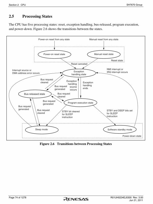
Section 2 CPU
Page 74 of 1278 R01UH0234EJ0300 Rev. 3.00 Jun 21, 2011
SH7670 Group
2.5 Processing States
The CPU has five processing states: reset, exception handling, bus-released, program execution, and power-down. Figure 2.6 shows the transitions between the states.
Power-on reset from any state Manual reset from any state
Power-on reset state Manual reset state
Program execution state
Sleep mode Software standby mode
Exceptionhandling state
Exceptionhandling
sourceoccurs
Exceptionhandlingends
NMI interrupt or IRQ interrupt occurs
Power-down state
Reset canceled
STBY bit clearedfor SLEEPinstruction
Reset state
Interrupt source or DMA address error occurs
STBY and DEEP bits setfor SLEEPinstruction
Bus-released state
Bus requestgenerated Bus request
cleared
Bus requestgenerated
Bus requestcleared
Bus requestcleared
Bus requestgenerated
Figure 2.6 Transitions between Processing States

Section 2 CPU
R01UH0234EJ0300 Rev. 3.00 Page 75 of 1278 Jun 21, 2011
SH7670 Group
(1) Reset State
In the reset state, the CPU is reset. There are two kinds of reset, power-on reset and manual reset.
(2) Exception Handling State
The exception handling state is a transient state that occurs when exception handling sources such as resets or interrupts alter the CPU’s processing state flow.
For a reset, the initial values of the program counter (PC) (execution start address) and stack pointer (SP) are fetched from the exception handling vector table and stored; the CPU then branches to the execution start address and execution of the program begins.
For an interrupt, the stack pointer (SP) is accessed and the program counter (PC) and status register (SR) are saved to the stack area. The exception service routine start address is fetched from the exception handling vector table; the CPU then branches to that address and the program starts executing, thereby entering the program execution state.
(3) Program Execution State
In the program execution state, the CPU sequentially executes the program.
(4) Power-Down State
In the power-down state, the CPU stops operating to reduce power consumption. The SLEEP instruction places the CPU in sleep mode or software standby mode.
(5) Bus-Released State
In the bus-released state, the CPU releases bus to a device that has requested it.

Section 2 CPU
Page 76 of 1278 R01UH0234EJ0300 Rev. 3.00 Jun 21, 2011
SH7670 Group
Section 3 Floating-Point Unit (FPU)
R01UH0234EJ0300 Rev. 3.00 Page 77 of 1278 Jun 21, 2011
SH7670 Group
Section 3 Floating-Point Unit (FPU)
3.1 Features
The FPU has the following features.
• Conforms to IEEE754 standard
• 16 single-precision floating-point registers (can also be referenced as eight double-precision registers)
• Two rounding modes: Round to nearest and round to zero
• Denormalization modes: Flush to zero
• Five exception sources: Invalid operation, divide by zero, overflow, underflow, and inexact
• Comprehensive instructions: Single-precision, double-precision, and system control
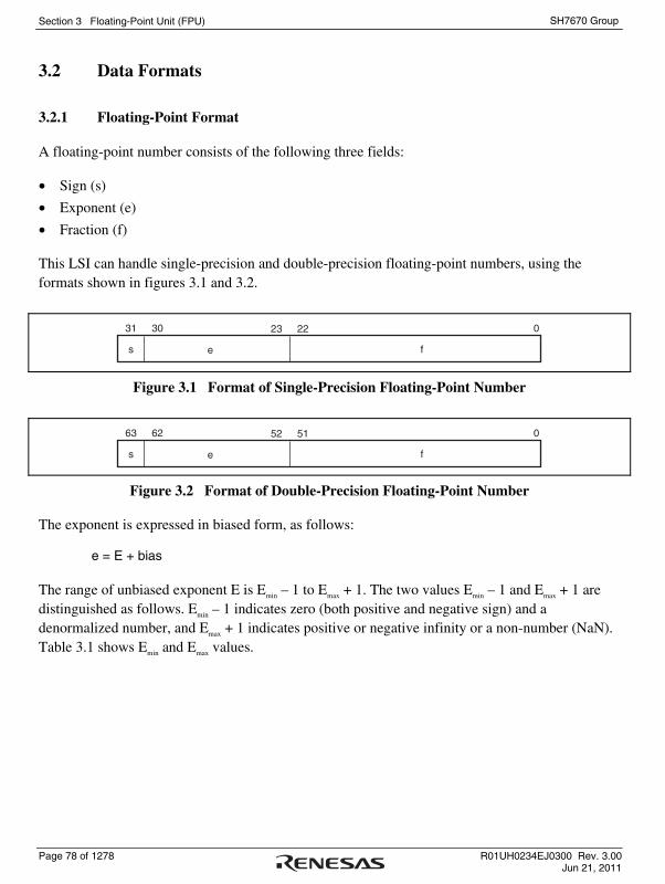
Section 3 Floating-Point Unit (FPU)
Page 78 of 1278 R01UH0234EJ0300 Rev. 3.00 Jun 21, 2011
SH7670 Group
3.2 Data Formats
3.2.1 Floating-Point Format
A floating-point number consists of the following three fields:
• Sign (s)
• Exponent (e)
• Fraction (f) This LSI can handle single-precision and double-precision floating-point numbers, using the formats shown in figures 3.1 and 3.2.
31 30 23 22 0
s e f
Figure 3.1 Format of Single-Precision Floating-Point Number
63 62 52 51 0
s e f
Figure 3.2 Format of Double-Precision Floating-Point Number
The exponent is expressed in biased form, as follows:
e = E + bias
The range of unbiased exponent E is Emin – 1 to Emax + 1. The two values Emin – 1 and Emax + 1 are distinguished as follows. Emin – 1 indicates zero (both positive and negative sign) and a denormalized number, and Emax + 1 indicates positive or negative infinity or a non-number (NaN). Table 3.1 shows Emin and Emax values.

Section 3 Floating-Point Unit (FPU)
R01UH0234EJ0300 Rev. 3.00 Page 79 of 1278 Jun 21, 2011
SH7670 Group
Table 3.1 Floating-Point Number Formats and Parameters
Parameter Single-Precision Double-Precision
Total bit width 32 bits 64 bits
Sign bit 1 bit 1 bit
Exponent field 8 bits 11 bits
Fraction field 23 bits 52 bits
Precision 24 bits 53 bits
Bias +127 +1023
Emax +127 +1023
Emin –126 –1022
Floating-point number value v is determined as follows:
If E = Emax + 1 and f ≠ 0, v is a non-number (NaN) irrespective of sign s
If E = Emax + 1 and f = 0, v = (–1)s (infinity) [positive or negative infinity]
If Emin ≤ E ≤ Emax , v = (–1)s2E (1.f) [normalized number]
If E = Emin – 1 and f ≠ 0, v = (–1)s2Emin (0.f) [denormalized number]
If E = Emin – 1 and f = 0, v = (–1)s0 [positive or negative zero]

Section 3 Floating-Point Unit (FPU)
Page 80 of 1278 R01UH0234EJ0300 Rev. 3.00 Jun 21, 2011
SH7670 Group
Table 3.2 shows the ranges of the various numbers in hexadecimal notation.
Table 3.2 Floating-Point Ranges
Type Single-Precision Double-Precision
Signaling non-number H'7FFF FFFF to H'7FC0 0000 H'7FFF FFFF FFFF FFFF to H'7FF8 0000 0000 0000
Quiet non-number H'7FBF FFFF to H'7F80 0001 H'7FF7 FFFF FFFF FFFF to H'7FF0 0000 0000 0001
Positive infinity H'7F80 0000 H'7FF0 0000 0000 0000
Positive normalized number
H'7F7F FFFF to H'0080 0000 H'7FEF FFFF FFFF FFFF to H'0010 0000 0000 0000
Positive denormalized number
H'007F FFFF to H'0000 0001 H'000F FFFF FFFF FFFF to H'0000 0000 0000 0001
Positive zero H'0000 0000 H'0000 0000 0000 0000
Negative zero H'8000 0000 H'8000 0000 0000 0000
Negative denormalized number
H'8000 0001 to H'807F FFFF H'8000 0000 0000 0001 to H'800F FFFF FFFF FFFF
Negative normalized number
H'8080 0000 to H'FF7F FFFF H'8010 0000 0000 0000 to H'FFEF FFFF FFFF FFFF
Negative infinity H'FF80 0000 H'FFF0 0000 0000 0000
Quiet non-number H'FF80 0001 to H'FFBF FFFF H'FFF0 0000 0000 0001 to H'FFF7 FFFF FFFF FFFF
Signaling non-number H'FFC0 0000 to H'FFFF FFFF H'FFF8 0000 0000 0000 to H'FFFF FFFF FFFF FFFF
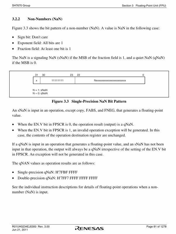
Section 3 Floating-Point Unit (FPU)
R01UH0234EJ0300 Rev. 3.00 Page 81 of 1278 Jun 21, 2011
SH7670 Group
3.2.2 Non-Numbers (NaN)
Figure 3.3 shows the bit pattern of a non-number (NaN). A value is NaN in the following case:
• Sign bit: Don't care
• Exponent field: All bits are 1
• Fraction field: At least one bit is 1 The NaN is a signaling NaN (sNaN) if the MSB of the fraction field is 1, and a quiet NaN (qNaN) if the MSB is 0.
31 30 23 22 0
x
N = 1: sNaNN = 0: qNaN
11111111 Nxxxxxxxxxxxxxxxxxxxxxx
Figure 3.3 Single-Precision NaN Bit Pattern
An sNaN is input in an operation, except copy, FABS, and FNEG, that generates a floating-point value.
• When the EN.V bit in FPSCR is 0, the operation result (output) is a qNaN.
• When the EN.V bit in FPSCR is 1, an invalid operation exception will be generated. In this case, the contents of the operation destination register are unchanged.
If a qNaN is input in an operation that generates a floating-point value, and an sNaN has not been input in that operation, the output will always be a qNaN irrespective of the setting of the EN.V bit in FPSCR. An exception will not be generated in this case.
The qNAN values as operation results are as follows:
• Single-precision qNaN: H'7FBF FFFF
• Double-precision qNaN: H'7FF7 FFFF FFFF FFFF See the individual instruction descriptions for details of floating-point operations when a non-number (NaN) is input.

Section 3 Floating-Point Unit (FPU)
Page 82 of 1278 R01UH0234EJ0300 Rev. 3.00 Jun 21, 2011
SH7670 Group
3.2.3 Denormalized Numbers
For a denormalized number floating-point value, the exponent field is expressed as 0, and the fraction field as a non-zero value.
In the SH2A-FPU, the DN bit in the status register FPSCR is always set to 1, therefore a denormalized number (source operand or operation result) is always flushed to 0 in a floating-point operation that generates a value (an operation other than copy, FNEG, or FABS).
When the DN bit in FPSCR is 0, a denormalized number (source operand or operation result) is processed as it is. See the individual instruction descriptions for details of floating-point operations when a denormalized number is input.

Section 3 Floating-Point Unit (FPU)
R01UH0234EJ0300 Rev. 3.00 Page 83 of 1278 Jun 21, 2011
SH7670 Group
3.3 Register Descriptions
3.3.1 Floating-Point Registers
Figure 3.4 shows the floating-point register configuration. There are sixteen 32-bit floating-point registers FPR0 to FPR15, referenced by specifying FR0 to FR15, DR0/2/4/6/8/10/12/14. The correspondence between FRPn and the reference name is determined by the PR and SZ bits in FPSCR. Refer figure 3.4.
1. Floating-point registers, FPRi (16 registers)
FPR0 to FPR15
2. Single-precision floating-point registers, FRi (16 registers)
FR0 to FR15 indicate FPR0 to FPR15
3. Double-precision floating-point registers or single-precision floating-point vector registers in pairs, DRi (8 registers)
A DR register comprises two FR registers.
DR0 = {FR0, FR1}, DR2 = {FR2, FR3}, DR4 = {FR4, FR5}, DR6 = {FR6, FR7}, DR8 = {FR8, FR9}, DR10 = {FR10, FR11}, DR12 = {FR12, FR13}, DR14 = {FR14, FR15}
FPR0FPR1FPR2FPR3FPR4FPR5FPR6FPR7FPR8FPR9FPR10FPR11FPR12FPR13FPR14FPR15
FR0 FR1 FR2 FR3 FR4 FR5FR6FR7FR8FR9FR10FR11FR12FR13FR14FR15
DR0
DR2
DR4
DR6
DR8
DR10
DR12
DR14
Transfer instruction case: FPSCR.SZ = 0 FPSCR.SZ = 1Operation instruction case: FPSCR.PR = 0 FPSCR.PR = 1
Register nameReference name
Figure 3.4 Floating-Point Registers
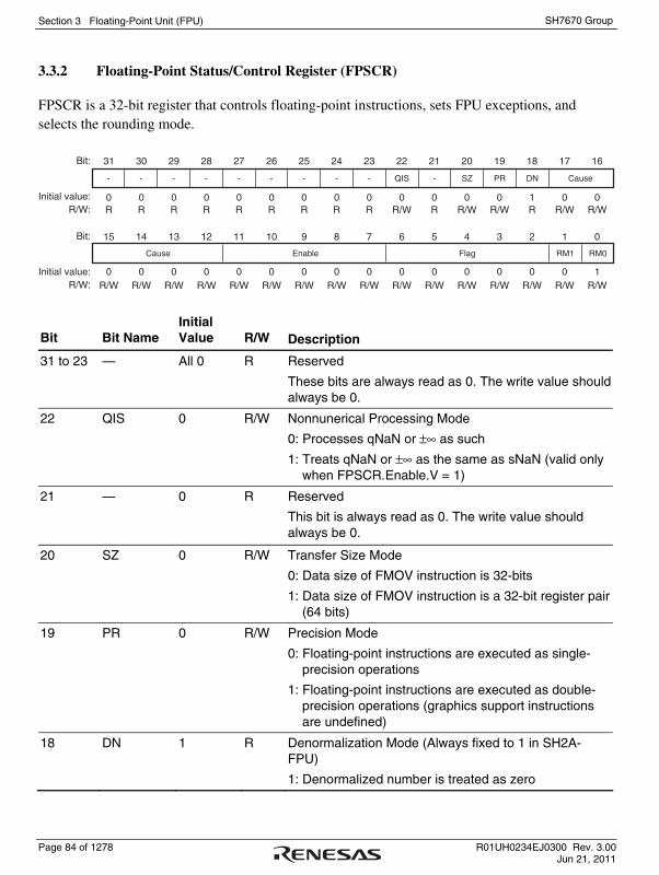
Section 3 Floating-Point Unit (FPU)
Page 84 of 1278 R01UH0234EJ0300 Rev. 3.00 Jun 21, 2011
SH7670 Group
3.3.2 Floating-Point Status/Control Register (FPSCR)
FPSCR is a 32-bit register that controls floating-point instructions, sets FPU exceptions, and selects the rounding mode.
31 30 29 28 27 26 25 24 23 22 21 20 19 18 17 16
15 14 13 12 11 10 9 8 7 6 5 4 3 2 1 0
0 0 0 0 0 0 0 0 0 0 0 0 0 1 0 0R R R R R R R R R R/W R R/W R/W R R/W R/W
0 0 0 0 0 0 0 0 0 0 0 0 0 0 0 1R/W R/W R/W R/W R/W R/W R/W R/W R/W R/W R/W R/W R/W R/W R/W R/W
Bit:
Initial value:R/W:
Bit:
Initial value:R/W:
- - - - - - - - - QIS - SZ PR DN Cause
Cause Enable Flag RM1 RM0
Bit Bit Name Initial Value R/W Description
31 to 23 — All 0 R Reserved
These bits are always read as 0. The write value should always be 0.
22 QIS 0 R/W Nonnunerical Processing Mode
0: Processes qNaN or ±∞ as such
1: Treats qNaN or ±∞ as the same as sNaN (valid only when FPSCR.Enable.V = 1)
21 — 0 R Reserved
This bit is always read as 0. The write value should always be 0.
20 SZ 0 R/W Transfer Size Mode
0: Data size of FMOV instruction is 32-bits
1: Data size of FMOV instruction is a 32-bit register pair (64 bits)
19 PR 0 R/W Precision Mode
0: Floating-point instructions are executed as single-precision operations
1: Floating-point instructions are executed as double-precision operations (graphics support instructions are undefined)
18 DN 1 R Denormalization Mode (Always fixed to 1 in SH2A-FPU)
1: Denormalized number is treated as zero
Section 3 Floating-Point Unit (FPU)
R01UH0234EJ0300 Rev. 3.00 Page 85 of 1278 Jun 21, 2011
SH7670 Group
Bit Bit Name Initial Value R/W Description
17 to 12 Cause All 0 R/W
11 to 7 Enable All 0 R/W
6 to 2 Flag All 0 R/W
FPU Exception Cause Field
FPU Exception Enable Field
FPU Exception Flag Field
When an FPU exception occurs, the bits corresponding to the FPU exception cause field and FPU exception flag field are set to 1. Each time an FPU operation instruction is executed, the FPU exception cause field is cleared to 0. The FPU exception flag field remains set to 1 until it is cleared to 0 by software.
For bit allocations of each field, see table 3.3.
1
0
RM1
RM0
0
1
R/W
R/W
Rounding Mode These bits select the rounding mode.
00: Round to Nearest
01: Round to Zero
10: Reserved
11: Reserved
Table 3.3 Bit Allocation for FPU Exception Handling
Field Name
FPU Error (E)
Invalid Operation (V)
Division by Zero (Z)
Overflow (O)
Underflow (U)
Inexact (I)
Cause FPU exception cause field
Bit 17 Bit 16 Bit 15 Bit 14 Bit 13 Bit 12
Enable FPU exception enable field
None Bit 11 Bit 10 Bit 9 Bit 8 Bit 7
Flag FPU exception flag field
None Bit 6 Bit 5 Bit 4 Bit 3 Bit 2
Note: No FPU error occurs in the SH2A-FPU.
3.3.3 Floating-Point Communication Register (FPUL)
Information is transferred between the FPU and CPU via FPUL. FPUL is a 32-bit system register that is accessed from the CPU side by means of LDS and STS instructions. For example, to convert the integer stored in general register R1 to a single-precision floating-point number, the processing flow is as follows:
R1 → (LDS instruction) → FPUL → (single-precision FLOAT instruction) → FR1
Section 3 Floating-Point Unit (FPU)
Page 86 of 1278 R01UH0234EJ0300 Rev. 3.00 Jun 21, 2011
SH7670 Group
3.4 Rounding
In a floating-point instruction, rounding is performed when generating the final operation result from the intermediate result. Therefore, the result of combination instructions such as FMAC will differ from the result when using a basic instruction such as FADD, FSUB, or FMUL. Rounding is performed once in FMAC, but twice in FADD, FSUB, and FMUL.
Which of the two rounding methods is to be used is determined by the RM bits in FPSCR.
FPSCR.RM[1:0] = 00: Round to Nearest FPSCR.RM[1:0] = 01: Round to Zero
(1) Round to Nearest
The operation result is rounded to the nearest expressible value. If there are two nearest expressible values, the one with an LSB of 0 is selected.
If the unrounded value is 2Emax (2 – 2–P) or more, the result will be infinity with the same sign as the unrounded value. The values of Emax and P, respectively, are 127 and 24 for single-precision, and 1023 and 53 for double-precision.
(2) Round to Zero
The digits below the round bit of the unrounded value are discarded.
If the unrounded value is larger than the maximum expressible absolute value, the value will become the maximum expressible absolute value.

Section 3 Floating-Point Unit (FPU)
R01UH0234EJ0300 Rev. 3.00 Page 87 of 1278 Jun 21, 2011
SH7670 Group
3.5 Floating-Point Exceptions
3.5.1 FPU Exception Sources
The exception sources are as follows:
• FPU error (E): When FPSCR.DN = 0 and a denormalized number is input (No error occurs in the SH2A-FPU)
• Invalid operation (V): In case of an invalid operation, such as NaN input
• Division by zero (Z): Division with a zero divisor
• Overflow (O): When the operation result overflows
• Underflow (U): When the operation result underflows
• Inexact exception (I): When overflow, underflow, or rounding occurs The FPU exception cause field in FPSCR contains bits corresponding to all of above sources E, V, Z, O, U, and I, and the FPU exception flag and enable fields in FPSCR contain bits corresponding to sources V, Z, O, U, and I, but not E. Thus, FPU errors cannot be disabled.
When an FPU exception occurs, the corresponding bit in the FPU exception cause field is set to 1, and 1 is added to the corresponding bit in the FPU exception flag field. When an FPU exception does not occur, the corresponding bit in the FPU exception cause field is cleared to 0, but the corresponding bit in the FPU exception flag field remains unchanged.

Section 3 Floating-Point Unit (FPU)
Page 88 of 1278 R01UH0234EJ0300 Rev. 3.00 Jun 21, 2011
SH7670 Group
3.5.2 FPU Exception Handling
FPU exception handling is initiated in the following cases:
• FPU error (E): FPSCR.DN = 0 and a denormalized number is input (No error occurs in the SH2A-FPU)
• Invalid operation (V): FPSCR.Enable.V = 1 and invalid operation
• Division by zero (Z): FPSCR.Enable.Z = 1 and division with a zero divisor
• Overflow (O): FPSCR.Enable.O = 1 and instruction with possibility of operation result overflow
• Underflow (U): FPSCR.Enable.U = 1 and instruction with possibility of operation result underflow
• Inexact exception (I): FPSCR.Enable.I = 1 and instruction with possibility of inexact operation result
These possibilities are shown in the individual instruction descriptions. All exception events that originate in the FPU are assigned as the same exception event. The meaning of an exception is determined by software by reading from FPSCR and interpreting the information it contains. If no bits are set in the FPU exception cause field of FPSCR when one or more of bits O, U, I, and V are set in the FPU exception enable field, this indicates that an actual exception source is not generated. Also, the destination register is not changed by any FPU exception handling operation.
Except for the above, the FPU disables exception handling. In every processing, the bit corresponding to source V, Z, O, U, or I is set to 1, and a default value is generated as the operation result.
• Invalid operation (V): qNaN is generated as the result.
• Division by zero (Z): Infinity with the same sign as the unrounded value is generated.
• Overflow (O):
When rounding mode = RZ, the maximum normalized number, with the same sign as the unrounded value, is generated. When rounding mode = RN, infinity with the same sign as the unrounded value is generated.
• Underflow (U): Zero with the same sign as the unrounded value is generated.
• Inexact exception (I): An inexact result is generated.

Section 4 Cache
R01UH0234EJ0300 Rev. 3.00 Page 89 of 1278 Jun 21, 2011
SH7670 Group
Section 4 Cache
4.1 Features
• Capacity
Instruction cache: 8 Kbytes
Operand cache: 8 Kbytes
• Structure: Instructions/data separated, 4-way set associative
• Cache lock function (only for operand cache): Way 2 and way 3 are lockable
• Line size: 16 bytes
• Number of entries: 128 entries/way
• Write system: Write-back/write-through selectable
• Replacement method: Least-recently-used (LRU) algorithm
4.1.1 Cache Structure
The cache separates data and instructions and uses a 4-way set associative system. It is composed of four ways (banks), each of which is divided into an address section and a data section.
Each of the address and data sections is divided into 128 entries. The data section of the entry is called a line. Each line consists of 16 bytes (4 bytes × 4). The data capacity per way is 2 Kbytes (16 bytes × 128 entries), with a total of 8 Kbytes in the cache as a whole (4 ways). Figure 4.1 shows the operand cache structure. The instruction cache structure is the same as the operand cache structure except for not having the U bit.

Section 4 Cache
Page 90 of 1278 R01UH0234EJ0300 Rev. 3.00 Jun 21, 2011
SH7670 Group
0
1
127
V U LW0 LW1 LW2 LW3 0
1
127
LRU
23 (1 + 1 + 21) bits 128 (32 × 4) bits 6 bits
LW0 to LW3: Longword data 0 to 3
Entry 0
Entry 1
Entry 127
Tag address
Address array (ways 0 to 3) Data array (ways 0 to 3)
.
.
.
.
.
.
.
.
.
.
.
.
.
.
.
.
.
.
Figure 4.1 Operand Cache Structure
(1) Address Array
The V bit indicates whether the entry data is valid. When the V bit is 1, data is valid; when 0, data is not valid.
The U bit (only for operand cache) indicates whether the entry has been written to in write-back mode. When the U bit is 1, the entry has been written to; when 0, it has not.
The tag address holds the physical address used in the external memory access. It consists of 21 bits (address bits 31 to 11) used for comparison during cache searches. In this LSI, the addresses of the cache-enabled space are H'00000000 to H'1FFFFFFF (see section 7, Bus State Controller (BSC)), and therefore the upper three bits of the tag address are cleared to 0.
The V and U bits are initialized to 0 by a power-on reset but not initialized by a manual reset or in software standby mode. The tag address is not initialized by a power-on reset or manual reset or in software standby mode.
(2) Data Array
Holds a 16-byte instruction or data. Entries are registered in the cache in line units (16 bytes).
The data array is not initialized by a power-on reset or manual reset or in software standby mode.

Section 4 Cache
R01UH0234EJ0300 Rev. 3.00 Page 91 of 1278 Jun 21, 2011
SH7670 Group
(3) LRU
With the 4-way set associative system, up to four instructions or data with the same entry address can be registered in the cache. When an entry is registered, LRU shows which of the four ways it is recorded in. There are six LRU bits, controlled by hardware. A least-recently-used (LRU) algorithm is used to select the way that has been least recently accessed.
Six LRU bits indicate the way to be replaced in case of a cache miss. The relationship between LRU and way replacement is shown in table 4.1 when the cache lock function (only for operand cache) is not used (concerning the case where the cache lock function is used, see section 4.2.2, Cache Control Register 2 (CCR2)). If a bit pattern other than those listed in table 4.1 is set in the LRU bits by software, the cache will not function correctly. When modifying the LRU bits by software, set one of the patterns listed in table 4.1.
The LRU bits are initialized to B'000000 by a power-on reset but not initialized by a manual reset or in software standby mode.
Table 4.1 LRU and Way Replacement (Cache Lock Function Not Used)
LRU (Bits 5 to 0) Way to be Replaced
000000, 000100, 010100, 100000, 110000, 110100 3
000001, 000011, 001011, 100001, 101001, 101011 2
000110, 000111, 001111, 010110, 011110, 011111 1
111000, 111001, 111011, 111100, 111110, 111111 0

Section 4 Cache
Page 92 of 1278 R01UH0234EJ0300 Rev. 3.00 Jun 21, 2011
SH7670 Group
4.2 Register Descriptions
The cache has the following registers.
Table 4.2 Register Configuration
Register Name Abbreviation R/W Initial Value Address Access Size
Cache control register 1 CCR1 R/W H'00000000 H'FFFC1000 32
Cache control register 2 CCR2 R/W H'00000000 H'FFFC1004 32
4.2.1 Cache Control Register 1 (CCR1)
The instruction cache is enabled or disabled using the ICE bit. The ICF bit controls disabling of all instruction cache entries. The operand cache is enabled or disabled using the OCE bit. The OCF bit controls disabling of all operand cache entries. The WT bit selects either write-through mode or write-back mode for operand cache.
Programs that change the contents of CCR1 should be placed in a cache-disabled space, and a cache-enabled space should be accessed after reading the contents of CCR1.
CCR1 is initialized to H'00000000 by a power-on reset but not initialized by a manual reset or in software standby mode.
31 30 29 28 27 26 25 24 23 22 21 20 19 18 17 16
15 14 13 12 11 10 9 8 7 6 5 4 3 2 1 0
0 0 0 0 0 0 0 0 0 0 0 0 0 0 0 0R R R R R R R R R R R R R R R R
0 0 0 0 0 0 0 0 0 0 0 0 0 0 0 0R R R R R/W R R R/W R R R R R/W R R/W R/W
Bit:
Initial value:R/W:
Bit:
Initial value:R/W:
- - - - - - - - - - - - - - - -
- - - - ICF - - ICE - - - - OCF - WT OCE

Section 4 Cache
R01UH0234EJ0300 Rev. 3.00 Page 93 of 1278 Jun 21, 2011
SH7670 Group
Bit Bit Name Initial Value R/W Description
31 to 12 ⎯ All 0 R Reserved
These bits are always read as 0. The write value should always be 0.
11 ICF 0 R/W Instruction Cache Flush
Writing 1 flushes all instruction cache entries (clears the V and LRU bits of all instruction cache entries to 0). Always reads 0. Write-back to external memory is not performed when the instruction cache is flushed.
10, 9 ⎯ All 0 R Reserved
These bits are always read as 0. The write value should always be 0.
8 ICE 0 R/W Instruction Cache Enable
Indicates whether the instruction cache function is enabled/disabled.
0: Instruction cache disable
1: Instruction cache enable
7 to 4 ⎯ All 0 R Reserved
These bits are always read as 0. The write value should always be 0.
3 OCF 0 R/W Operand Cache Flush
Writing 1 flushes all operand cache entries (clears the V, U, and LRU bits of all operand cache entries to 0). Always reads 0. Write-back to external memory is not performed when the operand cache is flushed.
2 ⎯ 0 R Reserved This bit is always read as 0. The write value should always be 0.
1 WT 0 R/W Write Through Selects write-back mode or write-through mode.
0: Write-back mode
1: Write-through mode
0 OCE 0 R/W Operand Cache Enable
Indicates whether the operand cache function is enabled/disabled.
0: Operand cache disable
1: Operand cache enable

Section 4 Cache
Page 94 of 1278 R01UH0234EJ0300 Rev. 3.00 Jun 21, 2011
SH7670 Group
4.2.2 Cache Control Register 2 (CCR2)
CCR2 is used to enable or disable the cache locking function for operand cache and is valid in cache locking mode only. In cache locking mode, the lock enable bit (the LE bit) in CCR2 is set to 1. In non-cache-locking mode, the cache locking function is invalid.
When a cache miss occurs in cache locking mode by executing the prefetch instruction (PREF @Rn), the line of data pointed to by Rn is loaded into the cache according to bits 9 and 8 (the W3LOAD and W3LOCK bits) and bits 1 and 0 (the W2LOAD and W2LOCK bits) in CCR2. The relationship between the setting of each bit and a way, to be replaced when the prefetch instruction is executed, are listed in table 4.3. On the other hand, when the prefetch instruction is executed and a cache hit occurs, new data is not fetched and the entry which is already enabled is held. For example, when the prefetch instruction is executed with W3LOAD = 1 and W3LOCK = 1 specified in cache locking mode while one-line data already exists in way 0 which is specified by Rn, a cache hit occurs and data is not fetched to way 3.
In the cache access other than the prefetch instruction in cache locking mode, ways to be replaced by bits W3LOCK and W2LOCK are restricted. The relationship between the setting of each bit in CCR2 and ways to be replaced are listed in table 4.4.
Programs that change the contents of CCR2 should be placed in a cache-disabled space, and a cache-enabled space should be accessed after reading the contents of CCR2.
CCR2 is initialized to H'00000000 by a power-on reset but not initialized by a manual reset or in software standby mode.
31 30 29 28 27 26 25 24 23 22 21 20 19 18 17 16
15 14 13 12 11 10 9 8 7 6 5 4 3 2 1 0
0 0 0 0 0 0 0 0 0 0 0 0 0 0 0 0R R R R R R R R R R R R R R R R/W
0 0 0 0 0 0 0 0 0 0 0 0 0 0 0 0R R R R R R R/W R/W R R R R R R R/W R/W
Bit:
Initial value:R/W:
Bit:
Initial value:R/W:
Note: The W3LOAD and W2LOAD bits should not be set to 1 at the same time.*
- - - - - - - - - - - - - - - LE
- - - - - - W3LOAD*
W3LOCK
W2LOAD*
W2LOCK- - - - - -
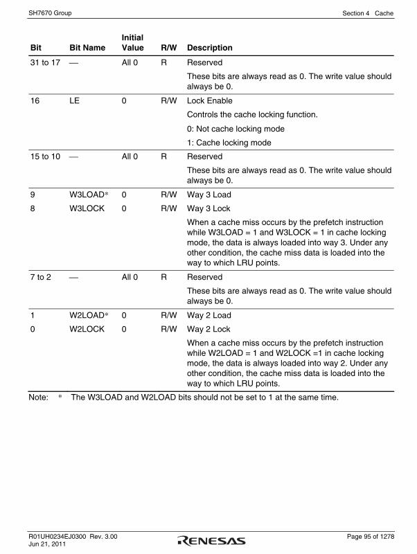
Section 4 Cache
R01UH0234EJ0300 Rev. 3.00 Page 95 of 1278 Jun 21, 2011
SH7670 Group
Bit Bit Name Initial Value R/W Description
31 to 17 ⎯ All 0 R Reserved
These bits are always read as 0. The write value should always be 0.
16 LE 0 R/W Lock Enable
Controls the cache locking function.
0: Not cache locking mode
1: Cache locking mode
15 to 10 ⎯ All 0 R Reserved
These bits are always read as 0. The write value should always be 0.
9
8
W3LOAD*
W3LOCK
0
0
R/W
R/W
Way 3 Load
Way 3 Lock
When a cache miss occurs by the prefetch instruction while W3LOAD = 1 and W3LOCK = 1 in cache locking mode, the data is always loaded into way 3. Under any other condition, the cache miss data is loaded into the way to which LRU points.
7 to 2 ⎯ All 0 R Reserved
These bits are always read as 0. The write value should always be 0.
1
0
W2LOAD*
W2LOCK
0
0
R/W
R/W
Way 2 Load
Way 2 Lock
When a cache miss occurs by the prefetch instruction while W2LOAD = 1 and W2LOCK =1 in cache locking mode, the data is always loaded into way 2. Under any other condition, the cache miss data is loaded into the way to which LRU points.
Note: * The W3LOAD and W2LOAD bits should not be set to 1 at the same time.

Section 4 Cache
Page 96 of 1278 R01UH0234EJ0300 Rev. 3.00 Jun 21, 2011
SH7670 Group
Table 4.3 Way to be Replaced when a Cache Miss Occurs in PREF Instruction
LE W3LOAD* W3LOCK W2LOAD* W2LOCK Way to be Replaced
0 x x x x Decided by LRU (table 4.1)
1 x 0 x 0 Decided by LRU (table 4.1)
1 x 0 0 1 Decided by LRU (table 4.5)
1 0 1 x 0 Decided by LRU (table 4.6)
1 0 1 0 1 Decided by LRU (table 4.7)
1 0 x 1 1 Way 2
1 1 1 0 x Way 3
[Legend]
x: Don't care
Note: * The W3LOAD and W2LOAD bits should not be set to 1 at the same time.
Table 4.4 Way to be Replaced when a Cache Miss Occurs in Other than PREF Instruction
LE W3LOAD* W3LOCK W2LOAD* W2LOCK Way to be Replaced
0 x x x x Decided by LRU (table 4.1)
1 x 0 x 0 Decided by LRU (table 4.1)
1 x 0 x 1 Decided by LRU (table 4.5)
1 x 1 x 0 Decided by LRU (table 4.6)
1 x 1 x 1 Decided by LRU (table 4.7)
[Legend]
x: Don't care Note: * The W3LOAD and W2LOAD bits should not be set to 1 at the same time.
Table 4.5 LRU and Way Replacement (when W2LOCK=1 and W3LOCK=0)
LRU (Bits 5 to 0) Way to be Replaced
000000, 000001, 000100, 010100, 100000, 100001, 110000, 110100 3
000011, 000110, 000111, 001011, 001111, 010110, 011110, 011111 1
101001, 101011, 111000, 111001, 111011, 111100, 111110, 111111 0

Section 4 Cache
R01UH0234EJ0300 Rev. 3.00 Page 97 of 1278 Jun 21, 2011
SH7670 Group
Table 4.6 LRU and Way Replacement (when W2LOCK=0 and W3LOCK=1)
LRU (Bits 5 to 0) Way to be Replaced
000000, 000001, 000011, 001011, 100000, 100001, 101001, 101011 2
000100, 000110, 000111, 001111, 010100, 010110, 011110, 011111 1
110000, 110100, 111000, 111001, 111011, 111100, 111110, 111111 0
Table 4.7 LRU and Way Replacement (when W2LOCK=1 and W3LOCK=1)
LRU (Bits 5 to 0) Way to be Replaced
000000, 000001, 000011, 000100, 000110, 000111, 001011, 001111, 010100, 010110, 011110, 011111
1
100000, 100001, 101001, 101011, 110000, 110100, 111000, 111001, 111011, 111100, 111110, 111111
0
Section 4 Cache
Page 98 of 1278 R01UH0234EJ0300 Rev. 3.00 Jun 21, 2011
SH7670 Group
4.3 Operation
Operations for the operand cache are described here. Operations for the instruction cache are similar to those for the operand cache except for the address array not having the U bit, and there being no prefetch operation or write operation, or a write-back buffer.
4.3.1 Searching Cache
If the operand cache is enabled (OCE bit in CCR1 is 1), whenever data in a cache-enabled area is accessed, the cache will be searched to see if the desired data is in the cache. Figure 4.2 illustrates the method by which the cache is searched.
Entries are selected using bits 10 to 4 of the address used to access memory and the tag address of that entry is read. At this time, the upper three bits of the tag address are always cleared to 0. Bits 31 to 11 of the address used to access memory are compared with the read tag address. The address comparison uses all four ways. When the comparison shows a match and the selected entry is valid (V = 1), a cache hit occurs. When the comparison does not show a match or the selected entry is not valid (V = 0), a cache miss occurs. Figure 4.2 shows a hit on way 1.

Section 4 Cache
R01UH0234EJ0300 Rev. 3.00 Page 99 of 1278 Jun 21, 2011
SH7670 Group
Entry 0 Entry 0
Entry 1
Entry 127
V U LW0 LW1 LW2 LW3
31 1011 4 3 2 1 0
CMP0 CMP1 CMP2 CMP3
.
.
.
.
.
.
.
.
.
Access address
Tag address
Address array(ways 0 to 3)
Data array(ways 0 to 3)
[Legend]
CMP0 to CMP3: Comparison circuits 0 to 3
Hit signal (way 1)
Entry selection Longword (LW) selection
Entry 127
Entry 1
.
.
.
.
.
.
.
.
.
Figure 4.2 Cache Search Scheme
Section 4 Cache
Page 100 of 1278 R01UH0234EJ0300 Rev. 3.00 Jun 21, 2011
SH7670 Group
4.3.2 Read Access
(1) Read Hit
In a read access, data is transferred from the cache to the CPU. LRU is updated so that the hit way is the latest.
(2) Read Miss
An external bus cycle starts and the entry is updated. The way replaced follows table 4.4. Entries are updated in 16-byte units. When the desired data that caused the miss is loaded from external memory to the cache, the data is transferred to the CPU in parallel with being loaded to the cache. When it is loaded in the cache, the V bit is set to 1, and LRU is updated so that the replaced way becomes the latest. In operand cache, the U bit is additionally cleared to 0. When the U bit of the entry to be replaced by updating the entry in write-back mode is 1, the cache update cycle starts after the entry is transferred to the write-back buffer. After the cache completes its update cycle, the write-back buffer writes the entry back to the memory. The write-back unit is 16 bytes.
4.3.3 Prefetch Operation (Only for Operand Cache)
(1) Prefetch Hit
LRU is updated so that the hit way becomes the latest. The contents in other caches are not modified. No data is transferred to the CPU.
(2) Prefetch Miss
No data is transferred to the CPU. The way to be replaced follows table 4.3. Other operations are the same in case of read miss.
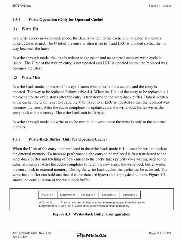
Section 4 Cache
R01UH0234EJ0300 Rev. 3.00 Page 101 of 1278 Jun 21, 2011
SH7670 Group
4.3.4 Write Operation (Only for Operand Cache)
(1) Write Hit
In a write access in write-back mode, the data is written to the cache and no external memory write cycle is issued. The U bit of the entry written is set to 1 and LRU is updated so that the hit way becomes the latest.
In write-through mode, the data is written to the cache and an external memory write cycle is issued. The U bit of the written entry is not updated and LRU is updated so that the replaced way becomes the latest.
(2) Write Miss
In write-back mode, an external bus cycle starts when a write miss occurs, and the entry is updated. The way to be replaced follows table 4.4. When the U bit of the entry to be replaced is 1, the cache update cycle starts after the entry is transferred to the write-back buffer. Data is written to the cache, the U bit is set to 1, and the V bit is set to 1. LRU is updated so that the replaced way becomes the latest. After the cache completes its update cycle, the write-back buffer writes the entry back to the memory. The write-back unit is 16 bytes.
In write-through mode, no write to cache occurs in a write miss; the write is only to the external memory.
4.3.5 Write-Back Buffer (Only for Operand Cache)
When the U bit of the entry to be replaced in the write-back mode is 1, it must be written back to the external memory. To increase performance, the entry to be replaced is first transferred to the write-back buffer and fetching of new entries to the cache takes priority over writing back to the external memory. After the cache completes to fetch the new entry, the write-back buffer writes the entry back to external memory. During the write-back cycles, the cache can be accessed. The write-back buffer can hold one line of cache data (16 bytes) and its physical address. Figure 4.3 shows the configuration of the write-back buffer.
Longword 0 Longword 1 Longword 2 Longword 3A (31 to 4)
A (31 to 4):Longword 0 to 3:
Physical address written to external memory (upper three bits are 0)One line of cache data to be written to external memory
Figure 4.3 Write-Back Buffer Configuration

Section 4 Cache
Page 102 of 1278 R01UH0234EJ0300 Rev. 3.00 Jun 21, 2011
SH7670 Group
Operations in sections 4.3.2 to 4.3.5 are compiled in table 4.8.
Table 4.8 Cache Operations
Cache CPU Cycle
Hit/
miss
Write-back mode/
write through mode U Bit
External Memory
Accession
(through internal bus) Cache Contents
Instructio
n cache
Instruction
fetch
Hit ⎯ ⎯ Not generated Not renewed
Miss ⎯ ⎯ Cache renewal cycle is
generated
Renewed to new values by
cache renewal cycle
Operand
cache
Prefetch/
read
Hit Either mode is
available x Not generated Not renewed
Miss Write-through mode ⎯ Cache renewal cycle is
generated
Renewed to new values by
cache renewal cycle
Write-back mode 0 Cache renewal cycle is
generated
Renewed to new values by
cache renewal cycle
1 Cache renewal cycle is
generated. Succeedingly
write-back cycle in write-back
buffer is generated.
Renewed to new values by
cache renewal cycle
Write Hit Write-through mode ⎯ Write cycle CPU issues is
generated.
Renewed to new values by write
cycle the CPU issues
Write-back mode x Not generated Renewed to new values by write
cycle the CPU issues
Miss Write-through mode ⎯ Write cycle CPU issues is
generated.
Not renewed*
Write-back mode 0 Cache renewal cycle is
generated
Renewed to new values by
cache renewal cycle.
Subsequently renewed again to
new values in write cycle CPU
issues.
1 Cache renewal cycle is
generated. Succeedingly
write-back cycle in write-back
buffer is generated.
Renewed to new values by
cache renewal cycle.
Subsequently renewed again to
new values in write cycle CPU
issues.
[Legend]
x: Don't care. Note: Cache renewal cycle: 16-byte read access, write-back cycle in write-back buffer: 16-byte
write access * Neither LRU renewed. LRU is renewed in all other cases.

Section 4 Cache
R01UH0234EJ0300 Rev. 3.00 Page 103 of 1278 Jun 21, 2011
SH7670 Group
4.3.6 Coherency of Cache and External Memory
Use software to ensure coherency between the cache and the external memory. When memory shared by this LSI and another device is mapped in the cache-enabled space, operate the memory-mapped cache to invalidate and write back as required.
Section 4 Cache
Page 104 of 1278 R01UH0234EJ0300 Rev. 3.00 Jun 21, 2011
SH7670 Group
4.4 Memory-Mapped Cache
To allow software management of the cache, cache contents can be read and written by means of MOV instructions. The instruction cache address array is mapped onto addresses H'F0000000 to H'F07FFFFF, and the data array onto addresses H'F1000000 to H'F17FFFFF. The operand cache address array is mapped onto addresses H'F0800000 to H'F0FFFFFF, and the data array onto addresses H'F1800000 to H'F1FFFFFF. Only longword can be used as the access size for the address array and data array, and instruction fetches cannot be performed.
4.4.1 Address Array
To access an address array, the 32-bit address field (for read/write accesses) and 32-bit data field (for write accesses) must be specified.
In the address field, specify the entry address selecting the entry, The W bit for selecting the way, and the A bit for specifying the existence of associative operation. In the W bit, B'00 is way 0, B'01 is way 1, B'10 is way 2, and B'11 is way 3. Since the access size of the address array is fixed at longword, specify B'00 for bits 1 and 0 of the address.
The tag address, LRU bits, U bit (only for operand cache), and V bit are specified as data. Always specify 0 for the upper three bits (bits 31 to 29) of the tag address.
For the address and data formats, see figure 4.4.
The following three operations are possible for the address array.
(1) Address Array Read
The tag address, LRU bits, U bit (only for operand cache), and V bit are read from the entry address specified by the address and the entry corresponding to the way. For the read operation, associative operation is not performed regardless of whether the associative bit (A bit) specified by the address is 1 or 0.
(2) Address-Array Write (Non-Associative Operation)
When the associative bit (A bit) in the address field is cleared to 0, write the tag address, LRU bits, U bit (only for operand cache), and V bit, specified by the data field, to the entry address specified by the address and the entry corresponding to the way. When writing to a cache line for which the U bit = 1 and the V bit =1 in the operand cache address array, write the contents of the cache line back to memory, then write the tag address, LRU bits, U bit, and V bit specified by the data field. When 0 is written to the V bit, 0 must also be written to the U bit of that entry.

Section 4 Cache
R01UH0234EJ0300 Rev. 3.00 Page 105 of 1278 Jun 21, 2011
SH7670 Group
(3) Address-Array Write (Associative Operation)
When writing with the associative bit (A bit) of the address field set to 1, the addresses in the four ways for the entry specified by the address field are compared with the tag address that is specified by the data field. Write the U bit (only for operand cache) and the V bit specified by the data field to the entry of the way that has a hit. However, the tag address and LRU bits remain unchanged. When there is no way that has a hit, nothing is written and there is no operation.
This function is used to invalidate a specific entry in the cache. When the U bit of the entry that has had a hit is 1 in the operand cache, writing back should be performed. However, when 0 is written to the V bit, 0 must also be written to the U bit of that entry.
4.4.2 Data Array
To access a data array, the 32-bit address field (for read/write accesses) and 32-bit data field (for write accesses) must be specified. The address field specifies information for selecting the entry to be accessed; the data field specifies the longword data to be written to the data array.
Specify the entry address for selecting the entry, the L bit indicating the longword position within the (16-byte) line, and the W bit for selecting the way. In the L bit, B'00 is longword 0, B'01 is longword 1, B'10 is longword 2, and B'11 is longword 3. In the W bit, B'00 is way 0, B'01 is way 1, B'10 is way 2, and B'11 is way 3. Since the access size of the data array is fixed at longword, specify B'00 for bits 1 and 0 of the address.
For the address and data formats, see figure 4.4.
The following two operations are possible for the data array. Information in the address array is not modified by this operation.
(1) Data Array Read
The data specified by the L bit in the address is read from the entry address specified by the address and the entry corresponding to the way.
(2) Data Array Write
The longword data specified by the data is written to the position specified by the L bit in the address from the entry address specified by the address and the entry corresponding to the way.

Section 4 Cache
Page 106 of 1278 R01UH0234EJ0300 Rev. 3.00 Jun 21, 2011
SH7670 Group
31 23 22 13 12 11
31 29 28
10 4 3 2 1 0
111100000
111100000
111100010
*----------*
*----------*
*----------*
*----------*
*----------*
*----------*
W *
LRU XX0 0 0 X VE
0 0 0
31 23 22 13 12 11 10 4 3 2 1 0
31 0
W 0L 0
31 23 22 13 12 11 10
11 10 9
4 3 2 1 0
4 3 2 1 0
W *A 0 0
31 23 22 13 12 11
31 29 28
10 4 3 2 1 0
111100001
111100001
111100011
W *
LRU XX0 0 0 U VE
0 0 0
31 23 22 13 12 11 10 4 3 2 1 0
31 0
W 0L 0
31 23 22 13 12 11 10
11 10 9
4 3 2 1 0
4 3 2 1 0
W *A 0 0
1. Instruction cache
1.1 Address array access
(a) Address specification
Read access
Write access
(b) Data specification (both read and write accesses)
1.2 Data array access (both read and write accesses)
(a) Address specification
Tag address (28 to 11)
Entry address
(b) Data specification
Longword data
*: Don't careE: Bit 10 of entry address for read, don't care for writeX: 0 for read, don't care for write
[Legend]
Entry address
Tag address (28 to 11)
Entry addressEntry address
Entry address
Entry address
Longword data
2.2 Data array access (both read and write accesses)
(a) Address specification
(b) Data specification
2. Operand cache
2.1 Address array access
(a) Address specification
Read access
Write access
(b) Data specification (both read and write accesses)
Figure 4.4 Specifying Address and Data for Memory-Mapped Cache Access

Section 4 Cache
R01UH0234EJ0300 Rev. 3.00 Page 107 of 1278 Jun 21, 2011
SH7670 Group
4.4.3 Usage Examples
(1) Invalidating Specific Entries
Specific cache entries can be invalidated by writing 0 to the entry's V bit in the memory mapping cache access. When the A bit is 1, the tag address specified by the write data is compared to the tag address within the cache selected by the entry address, and data is written to the bits V and U specified by the write data when a match is found. If no match is found, there is no operation. When the V bit of an entry in the address array is set to 0, the entry is written back if the entry's U bit is 1.
An example when a write data is specified in R0 and an address is specified in R1 is shown below.
; R0=H'0110 0010; tag address(28-11)=B'0 0001 0001 0000 0000 0, U=0, V=0
; R1=H'F080 0088; operand cache address array access, entry=B'000 1000, A=1
;
MOV.L R0,@R1
(2) Reading the Data of a Specific Entry
The data section of a specific cache entry can be read by the memory mapping cache access. The longword indicated in the data field of the data array in figure 4.4 is read into the register.
An example when an address is specified in R0 and data is read in R1 is shown below.
; R0=H'F100 004C; instruction cache data array access, entry=B'000 0100,
; Way=0, longword address=3
;
MOV.L @R0,R1

Section 4 Cache
Page 108 of 1278 R01UH0234EJ0300 Rev. 3.00 Jun 21, 2011
SH7670 Group
4.4.4 Notes
1. Programs that access memory-mapped operand cache should be placed in a cache-disabled space. Programs that access memory-mapped instruction cache should also be placed in a cache-disabled space and an on-chip peripheral module or an external address space (a cache-disabled address) should be read at least twice each at the beginning and end of the programs.
2. Rewriting the address array contents so that two or more ways are hit simultaneously is prohibited. Operation is not guaranteed if the address array contents are changed so that two or more ways are hit simultaneously.
3. Memory-mapped cache can be accessed only by the CPU and not by the DMAC. Registers can be accessed by the CPU and the DMAC.

Section 5 Exception Handling
R01UH0234EJ0300 Rev. 3.00 Page 109 of 1278 Jun 21, 2011
SH7670 Group
Section 5 Exception Handling
5.1 Overview
5.1.1 Types of Exception Handling and Priority
Exception handling is started by sources, such as resets, address errors, register bank errors, interrupts, and instructions. Table 5.1 shows their priorities. When several exception handling sources occur at once, they are processed according to the priority shown.
Table 5.1 Types of Exception Handling and Priority Order
Type Exception Handling Priority
Power-on reset Reset
Manual reset
CPU address error Address error DMAC address error
FPU exception
Integer division exception (division by zero)
Instruction
Integer division exception (overflow)
Bank underflow Register bank error Bank overflow
NMI
User break
H-UDI
IRQ
Direct memory access controller (DMAC)
USB2.0 host/function module (USB)
Compare match timer (CMT)
Bus state controller (BSC)
Watchdog timer (WDT)
Host interface (HIF)
Interrupt
On-chip peripheral modules
Encryption/decryption and forward error correction core conjunction DMAC (A-DMAC)
High
Low
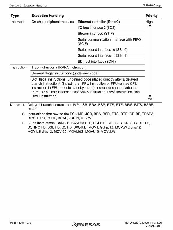
Section 5 Exception Handling
Page 110 of 1278 R01UH0234EJ0300 Rev. 3.00 Jun 21, 2011
SH7670 Group
Type Exception Handling Priority
Ethernet controller (EtherC)
I2C bus interface 3 (IIC3)
Stream interface (STIF)
Serial communication interface with FIFO (SCIF)
Serial sound interface_0 (SSI_0)
Serial sound interface_1 (SSI_1)
Interrupt On-chip peripheral modules
SD host interface (SDHI)
Trap instruction (TRAPA instruction)
General illegal instructions (undefined code)
Instruction
Slot illegal instructions (undefined code placed directly after a delayed branch instruction*1 (including an FPU instruction or FPU-related CPU instruction in FPU module standby mode), instructions that rewrite the PC*2, 32-bit instructions*3, RESBANK instruction, DIVS instruction, and DIVU instruction)
High
Low
Notes: 1. Delayed branch instructions: JMP, JSR, BRA, BSR, RTS, RTE, BF/S, BT/S, BSRF, BRAF.
2. Instructions that rewrite the PC: JMP, JSR, BRA, BSR, RTS, RTE, BT, BF, TRAPA, BF/S, BT/S, BSRF, BRAF, JSR/N, RTV/N.
3. 32-bit instructions: BAND.B, BANDNOT.B, BCLR.B, BLD.B, BLDNOT.B, BOR.B, BORNOT.B, BSET.B, BST.B, BXOR.B, MOV.B@disp12, MOV.W@disp12, MOV.L@disp12, MOVI20, MOVI20S, MOVU.B, MOVU.W.

Section 5 Exception Handling
R01UH0234EJ0300 Rev. 3.00 Page 111 of 1278 Jun 21, 2011
SH7670 Group
5.1.2 Exception Handling Operations
The exception handling sources are detected and begin processing according to the timing shown in table 5.2.
Table 5.2 Timing of Exception Source Detection and Start of Exception Handling
Exception Source Timing of Source Detection and Start of Handling
Power-on reset Starts when the RES pin changes from low to high, when the H-UDI reset negate command is set after the H-UDI reset assert command has been set, or when the WDT overflows.
Reset
Manual reset Starts when the WDT overflows.
Address error Detected when instruction is decoded and starts when the previous executing instruction finishes executing.
Interrupts Detected when instruction is decoded and starts when the previous executing instruction finishes executing.
Bank underflow Starts upon attempted execution of a RESBANK instruction when saving has not been performed to register banks.
Register bank error
Bank overflow In the state where saving has been performed to all register bank areas, starts when acceptance of register bank overflow exception has been set by the interrupt controller (the BOVE bit in IBNR of the INTC is 1) and an interrupt that uses a register bank has occurred and been accepted by the CPU.
Trap instruction Starts from the execution of a TRAPA instruction.
General illegal instructions
Starts from the decoding of an undefined code (including an FPU instruction or FPU-related CPU instruction in FPU module standby mode) anytime except immediately after a delayed branch instruction (delay slot).
Slot illegal instructions
Starts from the decoding of an undefined code placed (including an FPU instruction or FPU-related CPU instruction in FPU module standby mode) immediately after a delayed branch instruction (delay slot), of instructions that rewrite the PC, of 32-bit instructions, of the RESBANK instruction, of the DIVS instruction, or of the DIVU instruction.
Instructions
Integer division instructions
Starts when detecting division-by-zero exception or overflow exception caused by division of the negative maximum value (H'80000000) by −1.

Section 5 Exception Handling
Page 112 of 1278 R01UH0234EJ0300 Rev. 3.00 Jun 21, 2011
SH7670 Group
When exception handling starts, the CPU operates as follows:
(1) Exception Handling Triggered by Reset
The initial values of the program counter (PC) and stack pointer (SP) are fetched from the exception handling vector table (PC and SP are respectively the H'00000000 and H'00000004 addresses for power-on resets and the H'00000008 and H'0000000C addresses for manual resets). See section 5.1.3, Exception Handling Vector Table, for more information. The vector base register (VBR) is then initialized to H'00000000, the interrupt mask level bits (I3 to I0) of the status register (SR) are initialized to H'F (B'1111), and the BO and CS bits are initialized. The BN bit in IBNR of the interrupt controller (INTC) is also initialized to 0. The program begins running from the PC address fetched from the exception handling vector table.
(2) Exception Handling Triggered by Address Errors, Register Bank Errors, Interrupts, and Instructions
SR and PC are saved to the stack indicated by R15. In the case of interrupt exception handling other than NMI or user breaks with usage of the register banks enabled, general registers R0 to R14, control register GBR, system registers MACH, MACL, and PR, and the vector table address offset of the interrupt exception handling to be executed are saved to the register banks. In the case of exception handling due to an address error, register bank error, NMI interrupt, user break interrupt, or instruction, saving to a register bank is not performed. When saving is performed to all register banks, automatic saving to the stack is performed instead of register bank saving. In this case, an interrupt controller setting must have been made so that register bank overflow exceptions are not accepted (the BOVE bit in IBNR of the INTC is 0). If a setting to accept register bank overflow exceptions has been made (the BOVE bit in IBNR of the INTC is 1), register bank overflow exception will be generated. In the case of interrupt exception handling, the interrupt priority level is written to the I3 to I0 bits in SR. In the case of exception handling due to an address error or instruction, the I3 to I0 bits are not affected. The exception service routine start address is then fetched from the exception handling vector table and the program begins running from that address.

Section 5 Exception Handling
R01UH0234EJ0300 Rev. 3.00 Page 113 of 1278 Jun 21, 2011
SH7670 Group
5.1.3 Exception Handling Vector Table
Before exception handling begins running, the exception handling vector table must be set in memory. The exception handling vector table stores the start addresses of exception service routines. (The reset exception handling table holds the initial values of PC and SP.)
All exception sources are given different vector numbers and vector table address offsets, from which the vector table addresses are calculated. During exception handling, the start addresses of the exception service routines are fetched from the exception handling vector table, which is indicated by this vector table address.
Table 5.3 shows the vector numbers and vector table address offsets. Table 5.4 shows how vector table addresses are calculated.
Table 5.3 Exception Handling Vector Table
Exception Sources
Vector Numbers
Vector Table Address Offset
PC 0 H'00000000 to H'00000003 Power-on reset
SP 1 H'00000004 to H'00000007
PC 2 H'00000008 to H'0000000B Manual reset
SP 3 H'0000000C to H'0000000F
General illegal instruction 4 H'00000010 to H'00000013
(Reserved by system) 5 H'00000014 to H'00000017
Slot illegal instruction 6 H'00000018 to H'0000001B
7 H'0000001C to H'0000001F (Reserved by system)
8 H'00000020 to H'00000023
CPU address error 9 H'00000024 to H'00000027
DMAC address error 10 H'00000028 to H'0000002B
NMI 11 H'0000002C to H'0000002F Interrupts
User break 12 H'00000030 to H'00000033
FPU exception 13 H'00000034 to H'00000037
H-UDI 14 H'00000038 to H'0000003B
Bank overflow 15 H'0000003C to H'0000003F
Bank underflow 16 H'00000040 to H'00000043
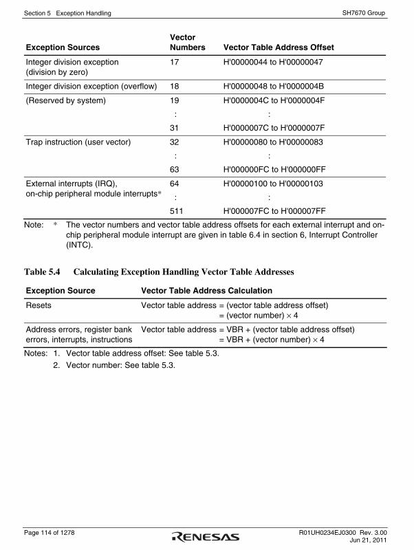
Section 5 Exception Handling
Page 114 of 1278 R01UH0234EJ0300 Rev. 3.00 Jun 21, 2011
SH7670 Group
Exception Sources
Vector Numbers
Vector Table Address Offset
Integer division exception (division by zero)
17 H'00000044 to H'00000047
Integer division exception (overflow) 18 H'00000048 to H'0000004B
(Reserved by system) 19
:
31
H'0000004C to H'0000004F
:
H'0000007C to H'0000007F
Trap instruction (user vector) 32
:
63
H'00000080 to H'00000083
:
H'000000FC to H'000000FF
External interrupts (IRQ), on-chip peripheral module interrupts*
64
:
511
H'00000100 to H'00000103
:
H'000007FC to H'000007FF
Note: * The vector numbers and vector table address offsets for each external interrupt and on-chip peripheral module interrupt are given in table 6.4 in section 6, Interrupt Controller (INTC).
Table 5.4 Calculating Exception Handling Vector Table Addresses
Exception Source Vector Table Address Calculation
Resets Vector table address = (vector table address offset) = (vector number) × 4
Address errors, register bank errors, interrupts, instructions
Vector table address = VBR + (vector table address offset) = VBR + (vector number) × 4
Notes: 1. Vector table address offset: See table 5.3.
2. Vector number: See table 5.3.

Section 5 Exception Handling
R01UH0234EJ0300 Rev. 3.00 Page 115 of 1278 Jun 21, 2011
SH7670 Group
5.2 Resets
5.2.1 Input/Output Pins
Table 5.5 shows the reset-related pin configuration.
Table 5.5 Pin Configuration
Pin Name Symbol I/O Function
Power-on reset RES Input When this pin is driven low, this LSI shifts to the power-on reset processing
5.2.2 Types of Reset
A reset is the highest-priority exception handling source. There are two kinds of reset, power-on and manual. As shown in table 5.6, the CPU state is initialized in both a power-on reset and a manual reset. The FPU state is initialized by a power-on reset, but not by a manual reset. On-chip peripheral module registers are initialized by a power-on reset, but not by a manual reset.
Table 5.6 Reset States
Conditions for Transition to Reset State Internal States
Type RES H-UDI Command MRES WDT Overflow CPU
On-Chip Peripheral Modules, I/O Port
WRCSR of WDT, FRQCR of CPG
Low — — — Initialized Initialized Initialized
High H-UDI reset assert command is set
— — Initialized Initialized Initialized
Power-on reset
High Command other than H-UDI reset assert is set
— Power-on reset
Initialized Initialized Not initialized
High Command other than H-UDI reset assert is set
Low — Initialized Not initialized* Not initialized Manual reset
High Command other than H-UDI reset assert is set
High Manual reset
Initialized Not initialized* Not initialized
Note: * The BN bit in IBNR of the INTC is initialized.

Section 5 Exception Handling
Page 116 of 1278 R01UH0234EJ0300 Rev. 3.00 Jun 21, 2011
SH7670 Group
5.2.3 Power-On Reset
(1) Power-On Reset by Means of RES Pin
When the RES pin is driven low, this LSI enters the power-on reset state. To reliably reset this LSI, the RES pin should be kept at the low level for the duration of the oscillation settling time at power-on or when in software standby mode (when the clock is halted), or at least 20-tcyc (unfixed) when the clock is running. In the power-on reset state, the internal state of the CPU and all the on-chip peripheral module registers are initialized. See appendix A, Pin States, for the status of individual pins during the power-on reset state.
In the power-on reset state, power-on reset exception handling starts when the RES pin is first driven low for a fixed period and then returned to high. The CPU operates as follows:
1. The initial value (execution start address) of the program counter (PC) is fetched from the exception handling vector table.
2. The initial value of the stack pointer (SP) is fetched from the exception handling vector table.
3. The vector base register (VBR) is cleared to H'00000000, the interrupt mask level bits (I3 to I0) of the status register (SR) are initialized to H'F (B'1111), and the BO and CS bits are initialized. The BN bit in IBNR of the INTC is also initialized to 0.
4. The values fetched from the exception handling vector table are set in the PC and SP, and the program begins executing.
Be certain to always perform power-on reset processing when turning the system power on.
(2) Power-On Reset by Means of H-UDI Reset Assert Command
When the H-UDI reset assert command is set, this LSI enters the power-on reset state. Power-on reset by means of an H-UDI reset assert command is equivalent to power-on reset by means of the RES pin. Setting the H-UDI reset negate command cancels the power-on reset state. The time required between an H-UDI reset assert command and H-UDI reset negate command is the same as the time to keep the RES pin low to initiate a power-on reset. In the power-on reset state generated by an H-UDI reset assert command, setting the H-UDI reset negate command starts power-on reset exception handling. The CPU operates in the same way as when a power-on reset was caused by the RES pin.

Section 5 Exception Handling
R01UH0234EJ0300 Rev. 3.00 Page 117 of 1278 Jun 21, 2011
SH7670 Group
(3) Power-On Reset Initiated by WDT
When a setting is made for a power-on reset to be generated in the WDT’s watchdog timer mode, and WTCNT of the WDT overflows, this LSI enters the power-on reset state.
In this case, WRCSR of the WDT and FRQCR of the CPG are not initialized by the reset signal generated by the WDT.
If a reset caused by the RES pin or the H-UDI reset assert command occurs simultaneously with a reset caused by WDT overflow, the reset caused by the RES pin or the H-UDI reset assert command has priority, and the WOVF bit in WRCSR is cleared to 0. When power-on reset exception processing is started by the WDT, the CPU operates in the same way as when a power-on reset was caused by the RES pin.
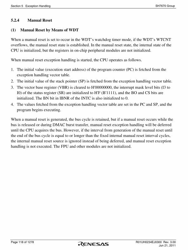
Section 5 Exception Handling
Page 118 of 1278 R01UH0234EJ0300 Rev. 3.00 Jun 21, 2011
SH7670 Group
5.2.4 Manual Reset
(1) Manual Reset by Means of WDT
When a manual reset is set to occur in the WDT’s watchdog timer mode, if the WDT’s WTCNT overflows, the manual reset state is established. In the manual reset state, the internal state of the CPU is initialized, but the registers in on-chip peripheral modules are not initialized.
When manual reset exception handling is started, the CPU operates as follows.
1. The initial value (execution start address) of the program counter (PC) is fetched from the exception handling vector table.
2. The initial value of the stack pointer (SP) is fetched from the exception handling vector table.
3. The vector base register (VBR) is cleared to H'00000000, the interrupt mask level bits (I3 to I0) of the status register (SR) are initialized to H'F (B'1111), and the BO and CS bits are initialized. The BN bit in IBNR of the INTC is also initialized to 0.
4. The values fetched from the exception handling vector table are set in the PC and SP, and the program begins executing.
When a manual reset is generated, the bus cycle is retained, but if a manual reset occurs while the bus is released or during DMAC burst transfer, manual reset exception handling will be deferred until the CPU acquires the bus. However, if the interval from generation of the manual reset until the end of the bus cycle is equal to or longer than the fixed internal manual reset interval cycles, the internal manual reset source is ignored instead of being deferred, and manual reset exception handling is not executed. The FPU and other modules are not initialized.

Section 5 Exception Handling
R01UH0234EJ0300 Rev. 3.00 Page 119 of 1278 Jun 21, 2011
SH7670 Group
5.3 Address Errors
5.3.1 Address Error Sources
Address errors occur when instructions are fetched or data read or written, as shown in table 5.7.
Table 5.7 Bus Cycles and Address Errors
Bus Cycle
Type
Bus Master
Bus Cycle Description
Address Errors
Instruction fetched from even address None (normal)
Instruction fetched from odd address Address error occurs
Instruction fetched from other than on-chip peripheral module space* or H'F0000000 to H'F5FFFFFF in on-chip RAM space*
None (normal)
Instruction fetch
CPU
Instruction fetched from on-chip peripheral module space* or H'F0000000 to H'F5FFFFFF in on-chip RAM space*
Address error occurs
Word data accessed from even address None (normal)
Word data accessed from odd address Address error occurs
Longword data accessed from a longword boundary
None (normal)
Longword data accessed from other than a long-word boundary
Address error occurs
Byte or word data accessed in on-chip peripheral module space*
None (normal)
Longword data accessed in 16-bit on-chip peripheral module space*
None (normal)
Data read/write
CPU or DMAC
Longword data accessed in 8-bit on-chip peripheral module space*
None (normal)
Note: * See section 7, Bus State Controller (BSC), for details of the on-chip peripheral module space and on-chip RAM space.

Section 5 Exception Handling
Page 120 of 1278 R01UH0234EJ0300 Rev. 3.00 Jun 21, 2011
SH7670 Group
5.3.2 Address Error Exception Handling
When an address error occurs, the bus cycle in which the address error occurred ends.* When the executing instruction then finishes, address error exception handling starts. The CPU operates as follows:
1. The exception service routine start address which corresponds to the address error that occurred is fetched from the exception handling vector table.
2. The status register (SR) is saved on the stack.
3. The program counter (PC) is saved on the stack. The PC value saved is the start address of the instruction to be executed after the last executed instruction.
4. After jumping to the exception service routine start address fetched from the exception handling vector table, program execution starts. The jump that occurs is not a delayed branch.
Note: This sequence only applies to address errors in the reading and writing of data. In case of
an address error due to instruction fetching, if the bus cycle in which the address error occurred is not completed by the end of step 3 above, address-error exception handling by the CPU is restarted. This continues until the bus cycle is complete.

Section 5 Exception Handling
R01UH0234EJ0300 Rev. 3.00 Page 121 of 1278 Jun 21, 2011
SH7670 Group
5.4 Register Bank Errors
5.4.1 Register Bank Error Sources
(1) Bank Overflow
In the state where saving has already been performed to all register bank areas, bank overflow occurs when acceptance of register bank overflow exception has been set by the interrupt controller (the BOVE bit in IBNR of the INTC is set to 1) and an interrupt that uses a register bank has occurred and been accepted by the CPU.
(2) Bank Underflow
Bank underflow occurs when an attempt is made to execute a RESBANK instruction while saving has not been performed to register banks.
5.4.2 Register Bank Error Exception Handling
When a register bank error occurs, register bank error exception handling starts. The CPU operates as follows:
1. The exception service routine start address which corresponds to the register bank error that occurred is fetched from the exception handling vector table.
2. The status register (SR) is saved to the stack.
3. The program counter (PC) is saved to the stack. The PC value saved is the start address of the instruction to be executed after the last executed instruction for a bank overflow, and the start address of the executed RESBANK instruction for a bank underflow.
To prevent multiple interrupts from occurring at a bank overflow, the interrupt priority level that caused the bank overflow is written to the interrupt mask level bits (I3 to I0) of the status register (SR).
4. After jumping to the exception service routine start address fetched from the exception handling vector table, program execution starts. The jump that occurs is not a delayed branch.
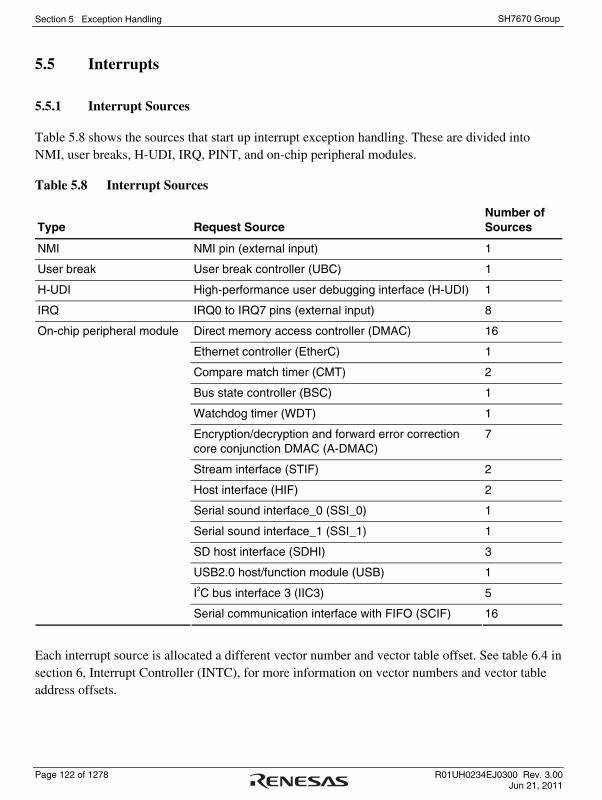
Section 5 Exception Handling
Page 122 of 1278 R01UH0234EJ0300 Rev. 3.00 Jun 21, 2011
SH7670 Group
5.5 Interrupts
5.5.1 Interrupt Sources
Table 5.8 shows the sources that start up interrupt exception handling. These are divided into NMI, user breaks, H-UDI, IRQ, PINT, and on-chip peripheral modules.
Table 5.8 Interrupt Sources
Type
Request Source
Number of Sources
NMI NMI pin (external input) 1
User break User break controller (UBC) 1
H-UDI High-performance user debugging interface (H-UDI) 1
IRQ IRQ0 to IRQ7 pins (external input) 8
Direct memory access controller (DMAC) 16
Ethernet controller (EtherC) 1
Compare match timer (CMT) 2
Bus state controller (BSC) 1
Watchdog timer (WDT) 1
Encryption/decryption and forward error correction core conjunction DMAC (A-DMAC)
7
Stream interface (STIF) 2
Host interface (HIF) 2
Serial sound interface_0 (SSI_0) 1
Serial sound interface_1 (SSI_1) 1
SD host interface (SDHI) 3
USB2.0 host/function module (USB) 1
I2C bus interface 3 (IIC3) 5
On-chip peripheral module
Serial communication interface with FIFO (SCIF) 16
Each interrupt source is allocated a different vector number and vector table offset. See table 6.4 in section 6, Interrupt Controller (INTC), for more information on vector numbers and vector table address offsets.

Section 5 Exception Handling
R01UH0234EJ0300 Rev. 3.00 Page 123 of 1278 Jun 21, 2011
SH7670 Group
5.5.2 Interrupt Priority Level
The interrupt priority order is predetermined. When multiple interrupts occur simultaneously (overlap), the interrupt controller (INTC) determines their relative priorities and starts processing according to the results.
The priority order of interrupts is expressed as priority levels 0 to 16, with priority 0 the lowest and priority 16 the highest. The NMI interrupt has priority 16 and cannot be masked, so it is always accepted. The user break interrupt and H-UDI interrupt priority level is 15. Priority levels of IRQ interrupts, and on-chip peripheral module interrupts can be set freely using the interrupt priority registers 01, 02, and 06 to 16 (IPR01, IPR02, and IPR06 to IPR16) of the INTC as shown in table 5.9. The priority levels that can be set are 0 to 15. Level 16 cannot be set. See section 6.3.1, Interrupt Priority Registers 01, 02, 06 to 16 (IPR01, IPR02, IPR06 to IPR16), for details of IPR01, IPR02, and IPR06 to IPR16.
Table 5.9 Interrupt Priority Order
Type Priority Level Comment
NMI 16 Fixed priority level. Cannot be masked.
User break 15 Fixed priority level.
H-UDI 15 Fixed priority level.
IRQ
On-chip peripheral module
0 to 15 Set with interrupt priority registers 01, 02, and 06 to 16 (IPR01, IPR02, and IPR06 to IPR16).
Section 5 Exception Handling
Page 124 of 1278 R01UH0234EJ0300 Rev. 3.00 Jun 21, 2011
SH7670 Group
5.5.3 Interrupt Exception Handling
When an interrupt occurs, its priority level is ascertained by the interrupt controller (INTC). NMI is always accepted, but other interrupts are only accepted if they have a priority level higher than the priority level set in the interrupt mask level bits (I3 to I0) of the status register (SR).
When an interrupt is accepted, interrupt exception handling begins. In interrupt exception handling, the CPU fetches the exception service routine start address which corresponds to the accepted interrupt from the exception handling vector table, and saves SR and the program counter (PC) to the stack. In the case of interrupt exception handling other than NMI or user breaks with usage of the register banks enabled, general registers R0 to R14, control register GBR, system registers MACH, MACL, and PR, and the vector table address offset of the interrupt exception handling to be executed are saved in the register banks. In the case of exception handling due to an address error, NMI interrupt, user break interrupt, or instruction, saving is not performed to the register banks. If saving has been performed to all register banks (0 to 14), automatic saving to the stack is performed instead of register bank saving. In this case, an interrupt controller setting must have been made so that register bank overflow exceptions are not accepted (the BOVE bit in IBNR of the INTC is 0). If a setting to accept register bank overflow exceptions has been made (the BOVE bit in IBNR of the INTC is 1), register bank overflow exception occurs. Next, the priority level value of the accepted interrupt is written to the I3 to I0 bits in SR. For NMI, however, the priority level is 16, but the value set in the I3 to I0 bits is H'F (level 15). Then, after jumping to the start address fetched from the exception handling vector table, program execution starts. The jump that occurs is not a delayed branch. See section 6.6, Operation, for further details of interrupt exception handling.

Section 5 Exception Handling
R01UH0234EJ0300 Rev. 3.00 Page 125 of 1278 Jun 21, 2011
SH7670 Group
5.6 Exceptions Triggered by Instructions
5.6.1 Types of Exceptions Triggered by Instructions
Exception handling can be triggered by trap instructions, general illegal instructions, slot illegal instructions, and integer division exceptions, as shown in table 5.10.
Table 5.10 Types of Exceptions Triggered by Instructions
Type Source Instruction Comment
Trap instruction TRAPA
Slot illegal instructions
Undefined code placed immediately after a delayed branch instruction (delay slot) (including the FPU instruction and FPU-related CPU instruction in FPU module standby mode), instructions that rewrite the PC, 32-bit instructions, RESBANK instruction, DIVS instruction, and DIVU instruction
Delayed branch instructions: JMP, JSR, BRA, BSR, RTS, RTE, BF/S, BT/S, BSRF, BRAF
Instructions that rewrite the PC: JMP, JSR, BRA, BSR, RTS, RTE, BT, BF, TRAPA, BF/S, BT/S, BSRF, BRAF, JSR/N, RTV/N
32-bit instructions: BAND.B, BANDNOT.B, BCLR.B, BLD.B, BLDNOT.B, BOR.B, BORNOT.B, BSET.B, BST.B, BXOR.B, MOV.B@disp12, MOV.W@disp12, MOV.L@disp12, MOVI20, MOVI20S, MOVU.B, MOVU.W.
General illegal instructions
Undefined code anywhere besides in a delay slot (including the FPU instruction and FPU-related CPU instruction in FPU module standby mode)
Division by zero DIVU, DIVS Integer division exceptions
Negative maximum value ÷ (−1) DIVS
Floating-point operation instruction
Instructions that will cause Invalid Operation Exception or Divide by Zero Exception defined in the IEEE754 standard, and instructions that may cause Overflow Exception, Underflow Exception, or Incorrectness Exception
FADD, FSUB, FMUL, FDIV, FMAC, FCMP/EQ, FCMP/GT, FLOAT, FTRC,FCNVDS, FCNVSD, FSQRT

Section 5 Exception Handling
Page 126 of 1278 R01UH0234EJ0300 Rev. 3.00 Jun 21, 2011
SH7670 Group
5.6.2 Trap Instructions
When a TRAPA instruction is executed, trap instruction exception handling starts. The CPU operates as follows:
1. The exception service routine start address which corresponds to the vector number specified in the TRAPA instruction is fetched from the exception handling vector table.
2. The status register (SR) is saved to the stack.
3. The program counter (PC) is saved to the stack. The PC value saved is the start address of the instruction to be executed after the TRAPA instruction.
4. After jumping to the exception service routine start address fetched from the exception handling vector table, program execution starts. The jump that occurs is not a delayed branch.
5.6.3 Slot Illegal Instructions
An instruction placed immediately after a delayed branch instruction is said to be placed in a delay slot. When the instruction placed in the delay slot is an undefined code (including an FPU instruction or FPU-related CPU instruction in FPU module standby mode), an instruction that rewrites the PC, a 32-bit instruction, an RESBANK instruction, a DIVS instruction, or a DIVU instruction, slot illegal exception handling starts if such kind of instruction is decoded. When the FPU is in the module standby state, the floating-point operation instruction and FPU-related CPU instruction are handled as an undefined code; when such an instruction is placed in the delay slot, slot illegal exception handling starts if the instruction is decoded. The CPU operates as follows:
1. The exception service routine start address is fetched from the exception handling vector table.
2. The status register (SR) is saved to the stack.
3. The program counter (PC) is saved to the stack. The PC value saved is the jump address of the delayed branch instruction immediately before the undefined code, the instruction that rewrites the PC, the 32-bit instruction, the RESBANK instruction, the DIVS instruction, or the DIVU instruction.
4. After jumping to the exception service routine start address fetched from the exception handling vector table, program execution starts. The jump that occurs is not a delayed branch.
5.6.4 General Illegal Instructions
When an undefined code (including an FPU instruction or FPU-related CPU instruction in FPU module standby mode) placed anywhere other than immediately after a delayed branch instruction (i.e., in a delay slot) is decoded, general illegal instruction exception handling starts. When the FPU is in the module standby state, the floating-point operation instruction and FPU-related CPU
Section 5 Exception Handling
R01UH0234EJ0300 Rev. 3.00 Page 127 of 1278 Jun 21, 2011
SH7670 Group
instruction are handled as an undefined code; when such an instruction is placed anywhere other than immediately after a delayed branch instruction (i.e., in a delay slot), general illegal instruction exception handling starts if the instruction is decoded.
The CPU handles general illegal instruction exception in the same way as slot illegal instruction exception. Unlike processing of slot illegal instruction exception, however, the program counter value stored is the start address of the undefined code.
5.6.5 Integer Division Instructions
When an integer division instruction performs division by zero or the result of integer division overflows, integer division instruction exception handling starts. The instructions that may become the source of division-by-zero exception are DIVU and DIVS. The only source instruction of overflow exception is DIVS, and overflow exception occurs only when the negative maximum value is divided by −1. The CPU operates as follows:
1. The exception service routine start address which corresponds to the integer division instruction exception that occurred is fetched from the exception handling vector table.
2. The status register (SR) is saved to the stack.
3. The program counter (PC) is saved to the stack. The PC value saved is the start address of the integer division instruction at which the exception occurred.
4. After jumping to the exception service routine start address fetched from the exception handling vector table, program execution starts. The jump that occurs is not a delayed branch.

Section 5 Exception Handling
Page 128 of 1278 R01UH0234EJ0300 Rev. 3.00 Jun 21, 2011
SH7670 Group
5.6.6 Floating-Point Operation Instruction
In the floating-point status/control register (FPSCR), FPU exception occurs if the V, Z, O, U, or I bit in the FPU exception enable field (Enable) is set. This indicates that a floating-point operation instruction has caused any of the exceptions defined in the IEEE754 standard: invalid operation exception, overflow exception (likely instruction), underflow exception (likely instruction), or incorrectness exception (likely instruction).
The following floating-point operation instructions may become exception sources:
FADD, FSUB, FMUL, FDIV, FMAC, FCMP/EQ, FCMP/GT, FLOAT, FTRC, FCNVDS, FCNVSD, FSQRT
An FPU exception occurs only when the corresponding enable bit is set. When the FPU detects an exception source, the FPU discontinues its operation and notifies the CPU of the occurrence of an exception. When exception handling is started, the CPU operates as follows:
1. The start address of the exception service routine corresponding to the FPU exception that has occurred is fetched from the exception handling vector table.
2. The status register (SR) is saved in the stack.
3. The program counter (PC) is saved in the stack. The start address of the instruction following the instruction executed last is the value to be saved in the PC.
4. To start executing the program, a jump occurs to the start address of the exception service routine fetched from the exception handling vector table. This jump is not a delayed branch.
The FPU exception flag filed (Flag) in the FPSCR is always updated irrespective of whether it is capable of accepting FPU exceptions and remains set until it is cleared explicitly by an instruction from the user. The FPU exception source field (Cause) in the FPSCR changes each time an FPU instruction is executed.
When the FPU exception enable field (Enable) in the FPSCR is set and when the QIS bit in the FPSCR is set, FPU exception starts if qNaN or ±∞ is entered into the source of the floating-point operation instruction.

Section 5 Exception Handling
R01UH0234EJ0300 Rev. 3.00 Page 129 of 1278 Jun 21, 2011
SH7670 Group
5.7 When Exception Sources Are Not Accepted
When an address error, FPU exception, register bank error (overflow), or interrupt is generated immediately after a delayed branch instruction, it is sometimes not accepted immediately but stored instead, as shown in table 5.11. When this happens, it will be accepted when an instruction that can accept the exception is decoded.
Table 5.11 Exception Source Generation Immediately after Delayed Branch Instruction
Exception Source
Point of Occurrence Address Error FPU exception
Register Bank Error (Overflow) Interrupt
Immediately after a delayed branch instruction*
Not accepted Not accepted Not accepted Not accepted
Note: * Delayed branch instructions: JMP, JSR, BRA, BSR, RTS, RTE, BF/S, BT/S, BSRF, BRAF

Section 5 Exception Handling
Page 130 of 1278 R01UH0234EJ0300 Rev. 3.00 Jun 21, 2011
SH7670 Group
5.8 Stack Status after Exception Handling Ends
The status of the stack after exception handling ends is as shown in table 5.12.
Table 5.12 Stack Status After Exception Handling Ends
Exception Type Stack Status
Address error
32 bits
32 bitsSR
Address of instructionafter executed instruction
SP
Interrupt
32 bits
32 bitsSR
Address of instructionafter executed instruction
SP
Register bank error (overflow)
32 bits
32 bitsSR
Address of instructionafter executed instructionSP
Register bank error (underflow)
32 bits
32 bitsSR
Start address of relevantRESBANK instruction
SP
Trap instruction
32 bits
32 bitsSR
Address of instructionafter TRAPA instructionSP
Slot illegal instruction
32 bits
32 bitsSR
Jump destination addressof delayed branch instructionSP
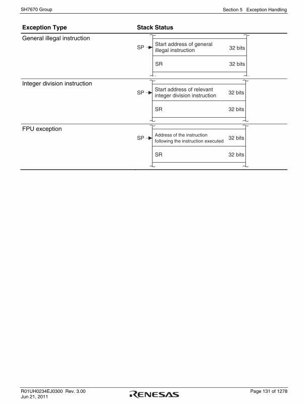
Section 5 Exception Handling
R01UH0234EJ0300 Rev. 3.00 Page 131 of 1278 Jun 21, 2011
SH7670 Group
Exception Type Stack Status
General illegal instruction
32 bits
32 bitsSR
Start address of general illegal instructionSP
Integer division instruction
32 bits
32 bitsSR
Start address of relevantinteger division instructionSP
FPU exception
32 bits
32 bitsSR
Address of the instruction following the instruction executed
SP

Section 5 Exception Handling
Page 132 of 1278 R01UH0234EJ0300 Rev. 3.00 Jun 21, 2011
SH7670 Group
5.9 Usage Notes
5.9.1 Value of Stack Pointer (SP)
The value of the stack pointer must always be a multiple of four. If it is not, an address error will occur when the stack is accessed during exception handling.
5.9.2 Value of Vector Base Register (VBR)
The value of the vector base register must always be a multiple of four. If it is not, an address error will occur when the stack is accessed during exception handling.
5.9.3 Address Errors Caused by Stacking of Address Error Exception Handling
When the stack pointer is not a multiple of four, an address error will occur during stacking of the exception handling (interrupts, etc.) and address error exception handling will start up as soon as the first exception handling is ended. Address errors will then also occur in the stacking for this address error exception handling. To ensure that address error exception handling does not go into an endless loop, no address errors are accepted at that point. This allows program control to be shifted to the address error exception service routine and enables error processing.
When an address error occurs during exception handling stacking, the stacking bus cycle (write) is executed. During stacking of the status register (SR) and program counter (PC), the SP is decremented by 4 for both, so the value of SP will not be a multiple of four after the stacking either. The address value output during stacking is the SP value, so the address where the error occurred is itself output. This means the write data stacked will be undefined.
Section 6 Interrupt Controller (INTC)
R01UH0234EJ0300 Rev. 3.00 Page 133 of 1278 Jun 21, 2011
SH7670 Group
Section 6 Interrupt Controller (INTC)
The interrupt controller (INTC) ascertains the priority of interrupt sources and controls interrupt requests to the CPU. The INTC registers set the order of priority of each interrupt, allowing the user to process interrupt requests according to the user-set priority.
6.1 Features
• 16 levels of interrupt priority can be set
By setting the nine interrupt priority registers, the priorities of IRQ interrupts, and on-chip peripheral module interrupts can be selected from 16 levels for request sources.
• NMI noise canceler function
An NMI input-level bit indicates the NMI pin state. By reading this bit in the interrupt exception service routine, the pin state can be checked, enabling it to be used as the noise canceler function.
• Register banks
This LSI has register banks that enable register saving and restoration required in the interrupt processing to be performed at high speed.

Section 6 Interrupt Controller (INTC)
Page 134 of 1278 R01UH0234EJ0300 Rev. 3.00 Jun 21, 2011
SH7670 Group
Figure 6.1 shows a block diagram of the INTC.
UBCH-UDIDMAC
CMTBSCWDT
MTU2MTU2S
POE2ADCIIC3
SCIF
UBC:H-UDI:DMAC:CMT:BSC:WDT:EtherC:A-DMAC:
HIF:USB:STIF:SSI:
SDHI:IIC3:SCIF: ICR0:ICR1:ICR2:IRQRR:PINTER:PIRR:IBCR:IBNR:IPR01, IPR02, IPR06 to IPR16:
SR
CPU
Module bus
I3 I2 I1 I0
PINTER
IBCRIPR01, IPR02,IPR06 to IPR16
ICR0
ICR2
PIRR
IBNR
ICR1
IRQRR
PINT7 to PINT0IRQ7 to IRQ0
NMI
IRQOUT
IPR
Input control
INTC
(Interrupt request)(Interrupt request)(Interrupt request)(Interrupt request)(Interrupt request)(Interrupt request)(Interrupt request)(Interrupt request)(Interrupt request)(Interrupt request)(Interrupt request)(Interrupt request)
Priorityidentifier
Com-parator
Interruptrequest
Businterface
Per
iphe
ral b
us
User break controllerHigh-performance user debugging interfaceDirect memory access controllerCompare match timerBus state controllerWatchdog timerEthernet controllerDMAC with encryption/decryption and forward error correction coreHost interfaceUSB2.0 host/function moduleStream interfaceSerial sound interface
SD host interfaceI2C bus interface 3Serial communication interface with FIFO Interrupt control register 0Interrupt control register 1Interrupt control register 2IRQ interrupt request registerPINT interrupt enable registerPINT interrupt request registerBank control registerBank number registerInterrupt priority registers 01, 02, 06 to 16
[Legend]
Figure 6.1 Block Diagram of INTC

Section 6 Interrupt Controller (INTC)
R01UH0234EJ0300 Rev. 3.00 Page 135 of 1278 Jun 21, 2011
SH7670 Group
6.2 Input/Output Pins
Table 6.1 shows the pin configuration of the INTC.
Table 6.1 Pin Configuration
Pin Name Symbol I/O Function
Nonmaskable interrupt input pin NMI Input Input of nonmaskable interrupt request signal
Interrupt request input pins IRQ7 to IRQ0 Input Input of maskable interrupt request signals

Section 6 Interrupt Controller (INTC)
Page 136 of 1278 R01UH0234EJ0300 Rev. 3.00 Jun 21, 2011
SH7670 Group
6.3 Register Descriptions
The INTC has the following registers. These registers are used to set the interrupt priorities and control detection of the external interrupt input signal.
Table 6.2 Register Configuration
Register Name Abbreviation R/W Initial Value Address
Access Size
Interrupt control register 0 ICR0 R/W *1 H'FFFE0800 16, 32
Interrupt control register 1 ICR1 R/W H'0000 H'FFFE0802 16, 32
IRQ interrupt request register IRQRR R/(W)*2 H'0000 H'FFFE0806 16, 32
Bank control register IBCR R/W H'0000 H'FFFE080C 16, 32
Bank number register IBNR R/W H'0000 H'FFFE080E 16, 32
Interrupt priority register 01 IPR01 R/W H'0000 H'FFFE0818 16, 32
Interrupt priority register 02 IPR02 R/W H'0000 H'FFFE081A 16, 32
Interrupt priority register 06 IPR06 R/W H'0000 H'FFFE0C00 16, 32
Interrupt priority register 07 IPR07 R/W H'0000 H'FFFE0C02 16, 32
Interrupt priority register 08 IPR08 R/W H'0000 H'FFFE0C04 16, 32
Interrupt priority register 09 IPR09 R/W H'0000 H'FFFE0C06 16, 32
Interrupt priority register 10 IPR10 R/W H'0000 H'FFFE0C08 16, 32
Interrupt priority register 11 IPR11 R/W H'0000 H'FFFE0C0A 16, 32
Interrupt priority register 12 IPR12 R/W H'0000 H'FFFE0C0C 16, 32
Interrupt priority register 13 IPR13 R/W H'0000 H'FFFE0C0E 16, 32
Interrupt priority register 14 IPR14 R/W H'0000 H'FFFE0C10 16, 32
Interrupt priority register 15 IPR15 R/W H'0000 H'FFFE0C12 16, 32
Interrupt priority register 16 IPR16 R/W H'0000 H'FFFE0C14 16, 32
Notes: 1. When the NMI pin is high, becomes H'8000; when low, becomes H'0000.
2. Only 0 can be written after reading 1, to clear the flag.

Section 6 Interrupt Controller (INTC)
R01UH0234EJ0300 Rev. 3.00 Page 137 of 1278 Jun 21, 2011
SH7670 Group
6.3.1 Interrupt Priority Registers 01, 02, 06 to 16 (IPR01, IPR02, IPR06 to IPR16)
IPR01, IPR02, and IPR06 to IPR16 are 16-bit readable/writable registers in which priority levels from 0 to 15 are set for IRQ interrupts, PINT interrupts, and on-chip peripheral module interrupts. Table 6.3 shows the correspondence between the interrupt request sources and the bits in IPR01, IPR02, and IPR06 to IPR16.
15 14 13 12 11 10 9 8 7 6 5 4 3 2 1 0
0 0 0 0 0 0 0 0 0 0 0 0 0 0 0 0R/W R/W R/W R/W R/W R/W R/W R/W R/W R/W R/W R/W R/W R/W R/W R/W
Bit:
Initial value:R/W:
Table 6.3 Interrupt Request Sources and IPR01, IPR02, and IPR06 to IPR16
Register Name Bits 15 to 12 Bits 11 to 8 Bits 7 to 4 Bits 3 to 0
Interrupt priority register 01
IRQ0 IRQ1 IRQ2 IRQ3
Interrupt priority register 02
IRQ4 IRQ5 IRQ6 IRQ7
Interrupt priority register 06
DMAC0 DMAC1 DMAC2 DMAC3
Interrupt priority register 07
DMAC4 DMAC5 DMAC6 DMAC7
Interrupt priority register 08
USB Reserved CMT0 CMT1
Interrupt priority register 09
BSC WDT HIF0 HIF1
Interrupt priority register 10
ADM1I C[0]I C[1]I Reserved
Interrupt priority register 11
Reserved Reserved FECI Reserved
Interrupt priority register 12
ETC IIC3 Reserved STIF0
Interrupt priority register 13
STIF1 SCIF0 SCIF1 SCIF2
Interrupt priority register 14
Reserved Reserved Reserved SSI0

Section 6 Interrupt Controller (INTC)
Page 138 of 1278 R01UH0234EJ0300 Rev. 3.00 Jun 21, 2011
SH7670 Group
Register Name Bits 15 to 12 Bits 11 to 8 Bits 7 to 4 Bits 3 to 0
Interrupt priority register 15
SSI1 Reserved Reserved Reserved
Interrupt priority register 16
Reserved SDHI Reserved Reserved
As shown in table 6.3, by setting the 4-bit groups (bits 15 to 12, bits 11 to 8, bits 7 to 4, and bits 3 to 0) with values from H'0 (0000) to H'F (1111), the priority of each corresponding interrupt is set. Setting of H'0 means priority level 0 (the lowest level) and H'F means priority level 15 (the highest level).
IPR01, IPR02, and IPR06 to IPR16 are initialized to H'0000 by a power-on reset.

Section 6 Interrupt Controller (INTC)
R01UH0234EJ0300 Rev. 3.00 Page 139 of 1278 Jun 21, 2011
SH7670 Group
6.3.2 Interrupt Control Register 0 (ICR0)
ICR0 is a 16-bit register that sets the input signal detection mode for the external interrupt input pin NMI, and indicates the input level at the NMI pin. ICR0 is initialized by a power-on reset.
15 14 13 12 11 10 9 8 7 6 5 4 3 2 1 0
* 0 0 0 0 0 0 0 0 0 0 0 0 0 0 0R R R R R R R R/W R R R R R R R R
Bit:
Initial value:R/W:
Note: 1 when the NMI pin is high, and 0 when the NMI pin is low.*
NMIL - - - - - - NMIE - - - - - - - -
Bit Bit Name Initial Value R/W Description
15 NMIL * R NMI Input Level
Sets the level of the signal input at the NMI pin. The NMI pin level can be obtained by reading this bit. This bit cannot be modified.
0: Low level is input to NMI pin
1: High level is input to NMI pin
14 to 9 ⎯ All 0 R Reserved
These bits are always read as 0. The write value should always be 0.
8 NMIE 0 R/W NMI Edge Select
Selects whether the falling or rising edge of the interrupt request signal on the NMI pin is detected.
0: Interrupt request is detected on falling edge of NMI
input
1: Interrupt request is detected on rising edge of NMI
input
7 to 0 ⎯ All 0 R Reserved
These bits are always read as 0. The write value should always be 0.
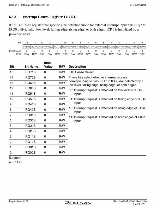
Section 6 Interrupt Controller (INTC)
Page 140 of 1278 R01UH0234EJ0300 Rev. 3.00 Jun 21, 2011
SH7670 Group
6.3.3 Interrupt Control Register 1 (ICR1)
ICR1 is a 16-bit register that specifies the detection mode for external interrupt input pins IRQ7 to IRQ0 individually: low level, falling edge, rising edge, or both edges. ICR1 is initialized by a power-on reset.
15 14 13 12 11 10 9 8 7 6 5 4 3 2 1 0
0 0 0 0 0 0 0 0 0 0 0 0 0 0 0 0R/W R/W R/W R/W R/W R/W R/W R/W R/W R/W R/W R/W R/W R/W R/W R/W
Bit:
Initial value:R/W:
IRQ71S IRQ70S IRQ61S IRQ60S IRQ51S IRQ50S IRQ41S IRQ40S IRQ31S IRQ30S IRQ21S IRQ20S IRQ11S IRQ10S IRQ01S IRQ00S
Bit Bit Name Initial Value R/W Description
15 IRQ71S 0 R/W
14 IRQ70S 0 R/W
13 IRQ61S 0 R/W
12 IRQ60S 0 R/W
11 IRQ51S 0 R/W
10 IRQ50S 0 R/W
9 IRQ41S 0 R/W
8 IRQ40S 0 R/W
7 IRQ31S 0 R/W
6 IRQ30S 0 R/W
5 IRQ21S 0 R/W
4 IRQ20S 0 R/W
3 IRQ11S 0 R/W
2 IRQ10S 0 R/W
1 IRQ01S 0 R/W
0 IRQ00S 0 R/W
IRQ Sense Select
These bits select whether interrupt signals corresponding to pins IRQ7 to IRQ0 are detected by a low level, falling edge, rising edge, or both edges.
00: Interrupt request is detected on low level of IRQn input
01: Interrupt request is detected on falling edge of IRQn input
10: Interrupt request is detected on rising edge of IRQn input
11: Interrupt request is detected on both edges of IRQn input
[Legend] n = 7 to 0

Section 6 Interrupt Controller (INTC)
R01UH0234EJ0300 Rev. 3.00 Page 141 of 1278 Jun 21, 2011
SH7670 Group
6.3.4 IRQ Interrupt Request Register (IRQRR)
IRQRR is a 16-bit register that indicates interrupt requests from external input pins IRQ7 to IRQ0. If edge detection is set for the IRQ7 to IRQ0 interrupts, writing 0 to the IRQ7F to IRQ0F bits after reading IRQ7F to IRQ0F = 1 cancels the retained interrupts.
IRQRR is initialized by a power-on reset.
15 14 13 12 11 10 9 8 7 6 5 4 3 2 1 0
0 0 0 0 0 0 0 0R/(W)* R/(W)* R/(W)* R/(W)* R/(W)* R/(W)* R/(W)* R/(W)*
Note: Only 0 can be written to clear the flag after 1 is read.*
Bit:
Initial value:R/W:
0 0 0 0 0 0 0 0R R R R R R R R
- - - - - - - - IRQ7F IRQ6F IRQ5F IRQ4F IRQ3F IRQ2F IRQ1F IRQ0F
Bit Bit Name Initial Value R/W Description
15 to 8 ⎯ All 0 R Reserved
These bits are always read as 0. The write value should always be 0.

Section 6 Interrupt Controller (INTC)
Page 142 of 1278 R01UH0234EJ0300 Rev. 3.00 Jun 21, 2011
SH7670 Group
Bit Bit Name Initial Value R/W Description
7 IRQ7F 0 R/(W)*
6 IRQ6F 0 R/(W)*
5 IRQ5F 0 R/(W)*
4 IRQ4F 0 R/(W)*
3 IRQ3F 0 R/(W)*
2 IRQ2F 0 R/(W)*
1 IRQ1F 0 R/(W)*
0 IRQ0F 0 R/(W)*
IRQ Interrupt Request
These bits indicate the status of the IRQ7 to IRQ0 interrupt requests.
Level detection:
0: IRQn interrupt request has not occurred [Clearing condition]
• IRQn input is high
1: IRQn interrupt has occurred
[Setting condition]
• IRQn input is low
Edge detection:
0: IRQn interrupt request is not detected
[Clearing conditions]
• Cleared by reading IRQnF while IRQnF = 1, then
writing 0 to IRQnF
• Cleared by executing IRQn interrupt exception
handling
1: IRQn interrupt request is detected [Setting condition]
• Edge corresponding to IRQn1S or IRQn0S of
ICR1 has occurred at IRQn pin
[Legend]
n = 7 to 0

Section 6 Interrupt Controller (INTC)
R01UH0234EJ0300 Rev. 3.00 Page 143 of 1278 Jun 21, 2011
SH7670 Group
6.3.5 Bank Control Register (IBCR)
IBCR is a 16-bit register that enables or disables use of register banks for each interrupt priority level. IBCR is initialized to H'0000 by a power-on reset.
15 14 13 12 11 10 9 8 7 6 5 4 3 2 1 0
0 0 0 0 0 0 0 0 0 0 0 0 0 0 0 0R/W R/W R/W R/W R/W R/W R/W R/W R/W R/W R/W R/W R/W R/W R/W R
Bit:
Initial value:R/W:
E15 E14 E13 E12 E11 E10 E9 E8 E7 E6 E5 E4 E3 E2 E1 -
Bit Bit Name Initial Value R/W Description
15 E15 0 R/W
14 E14 0 R/W
13 E13 0 R/W
12 E12 0 R/W
11 E11 0 R/W
10 E10 0 R/W
9 E9 0 R/W
8 E8 0 R/W
7 E7 0 R/W
6 E6 0 R/W
5 E5 0 R/W
4 E4 0 R/W
3 E3 0 R/W
2 E2 0 R/W
1 E1 0 R/W
Enable
These bits enable or disable use of register banks for interrupt priority levels 15 to 1. However, use of register banks is always disabled for the user break interrupts.
0: Use of register banks is disabled
1: Use of register banks is enabled
0 ⎯ 0 R Reserved
This bit is always read as 0. The write value should always be 0.
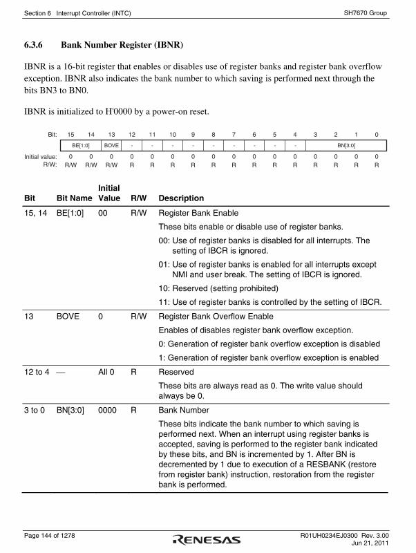
Section 6 Interrupt Controller (INTC)
Page 144 of 1278 R01UH0234EJ0300 Rev. 3.00 Jun 21, 2011
SH7670 Group
6.3.6 Bank Number Register (IBNR)
IBNR is a 16-bit register that enables or disables use of register banks and register bank overflow exception. IBNR also indicates the bank number to which saving is performed next through the bits BN3 to BN0.
IBNR is initialized to H'0000 by a power-on reset.
15 14 13 12 11 10 9 8 7 6 5 4 3 2 1 0
0 0 0 0 0 0 0 0 0 0 0 0 0 0 0 0R/W R/W R/W R R R R R R R R R R R R R
Bit:
Initial value:R/W:
BE[1:0] BOVE - - - - - - - - - BN[3:0]
Bit Bit Name Initial Value R/W Description
15, 14 BE[1:0] 00 R/W Register Bank Enable
These bits enable or disable use of register banks.
00: Use of register banks is disabled for all interrupts. The setting of IBCR is ignored.
01: Use of register banks is enabled for all interrupts except NMI and user break. The setting of IBCR is ignored.
10: Reserved (setting prohibited)
11: Use of register banks is controlled by the setting of IBCR.
13 BOVE 0 R/W Register Bank Overflow Enable
Enables of disables register bank overflow exception.
0: Generation of register bank overflow exception is disabled
1: Generation of register bank overflow exception is enabled
12 to 4 ⎯ All 0 R Reserved
These bits are always read as 0. The write value should always be 0.
3 to 0 BN[3:0] 0000 R Bank Number
These bits indicate the bank number to which saving is performed next. When an interrupt using register banks is accepted, saving is performed to the register bank indicated by these bits, and BN is incremented by 1. After BN is decremented by 1 due to execution of a RESBANK (restore from register bank) instruction, restoration from the register bank is performed.
Section 6 Interrupt Controller (INTC)
R01UH0234EJ0300 Rev. 3.00 Page 145 of 1278 Jun 21, 2011
SH7670 Group
6.4 Interrupt Sources
There are five types of interrupt sources: NMI, user break, H-UDI, IRQ, and on-chip peripheral modules. Each interrupt has a priority level (0 to 16), with 0 the lowest and 16 the highest. When set to level 0, that interrupt is masked at all times.
6.4.1 NMI Interrupt
The NMI interrupt has a priority level of 16 and is accepted at all times. NMI interrupt requests are edge-detected, and the NMI edge select bit (NMIE) in interrupt control register 0 (ICR0) selects whether the rising edge or falling edge is detected.
Though the priority level of the NMI interrupt is 16, the NMI interrupt exception handling sets the interrupt mask level bits (I3 to I0) in the status register (SR) to level 15.
6.4.2 User Break Interrupt
A user break interrupt which occurs when a break condition set in the user break controller (UBC) matches has a priority level of 15. The user break interrupt exception handling sets the I3 to I0 bits in SR to level 15. For user break interrupts, see section 25, User Break Controller (UBC).
6.4.3 H-UDI Interrupt
The high-performance user debugging interface (H-UDI) interrupt has a priority level of 15, and occurs at serial input of an H-UDI interrupt instruction. H-UDI interrupt requests are edge-detected and retained until they are accepted. The H-UDI interrupt exception handling sets the I3 to I0 bits in SR to level 15. For H-UDI interrupts, see section 26, High-Performance User Debugging Interface (H-UDI).

Section 6 Interrupt Controller (INTC)
Page 146 of 1278 R01UH0234EJ0300 Rev. 3.00 Jun 21, 2011
SH7670 Group
6.4.4 IRQ Interrupts
IRQ interrupts are input from pins IRQ7 to IRQ0. For the IRQ interrupts, low-level, falling-edge, rising-edge, or both-edge detection can be selected individually for each pin by the IRQ sense select bits (IRQ71S to IRQ01S and IRQ70S to IRQ00S) in interrupt control register 1 (ICR1). The priority level can be set individually in a range from 0 to 15 for each pin by interrupt priority registers 01 and 02 (IPR01 and IPR02).
When using low-level sensing for IRQ interrupts, an interrupt request signal is sent to the INTC while the IRQ7 to IRQ0 pins are low. An interrupt request signal is stopped being sent to the INTC when the IRQ7 to IRQ0 pins are driven high. The status of the interrupt requests can be checked by reading the IRQ interrupt request bits (IRQ7F to IRQ0F) in the IRQ interrupt request register (IRQRR).
When using edge-sensing for IRQ interrupts, an interrupt request is detected due to change of the IRQ7 to IRQ0 pin states, and an interrupt request signal is sent to the INTC. The result of IRQ interrupt request detection is retained until that interrupt request is accepted. Whether IRQ interrupt requests have been detected or not can be checked by reading the IRQ7F to IRQ0F bits in IRQRR. Writing 0 to these bits after reading them as 1 clears the result of IRQ interrupt request detection.
The IRQ interrupt exception handling sets the I3 to I0 bits in SR to the priority level of the accepted IRQ interrupt.
When returning from IRQ interrupt exception service routine, execute the RTE instruction after confirming that the interrupt request has been cleared by the IRQ interrupt request register (IRQRR) so as not to accidentally receive the interrupt request again.

Section 6 Interrupt Controller (INTC)
R01UH0234EJ0300 Rev. 3.00 Page 147 of 1278 Jun 21, 2011
SH7670 Group
6.4.5 On-Chip Peripheral Module Interrupts
On-chip peripheral module interrupts are generated by the following on-chip peripheral modules:
• Direct memory access controller (DMAC)
• Ethernet controller (EtherC)
• Compare match timer (CMT)
• Bus state controller (BSC)
• Watchdog timer (WDT)
• DMAC with encryption/decryption and forward error correction core (A-DMAC)
• Stream interface (STIF)
• Host interface (HIF)
• Serial sound interface (SSI)
• SD host interface (SDHI)
• USB2.0 host/function module (USB)
• I2C bus interface 3 (IIC3)
• Serial communication interface with FIFO (SCIF) As every source is assigned a different interrupt vector, the source does not need to be identified in the exception service routine. A priority level in a range from 0 to 15 can be set for each module by interrupt priority registers 06 to 16 (IPR06 to IPR16). The on-chip peripheral module interrupt exception handling sets the I3 to I0 bits in SR to the priority level of the accepted on-chip peripheral module interrupt.

Section 6 Interrupt Controller (INTC)
Page 148 of 1278 R01UH0234EJ0300 Rev. 3.00 Jun 21, 2011
SH7670 Group
6.5 Interrupt Exception Handling Vector Table and Priority
Table 6.4 lists interrupt sources and their vector numbers, vector table address offsets, and interrupt priorities.
Each interrupt source is allocated a different vector number and vector table address offset. Vector table addresses are calculated from the vector numbers and vector table address offsets. In interrupt exception handling, the interrupt exception service routine start address is fetched from the vector table indicated by the vector table address. For details of calculation of the vector table address, see table 5.4, Calculating Exception Handling Vector Table Addresses, in section 5, Exception Handling.
The priorities of IRQ interrupts, and on-chip peripheral module interrupts can be set freely between 0 and 15 for each pin or module by setting interrupt priority registers 01, 02, and 06 to 16 (IPR01, IPR02, and IPR06 to IPR16). However, if two or more interrupts specified by the same IPR among IPR06 to IPR16 occur, the priorities are defined as shown in the IPR setting unit internal priority of table 6.4, and the priorities cannot be changed. A power-on reset assigns priority level 0 to IRQ interrupts, and on-chip peripheral module interrupts. If the same priority level is assigned to two or more interrupt sources and interrupts from those sources occur simultaneously, they are processed by the default priorities indicated in table 6.4.
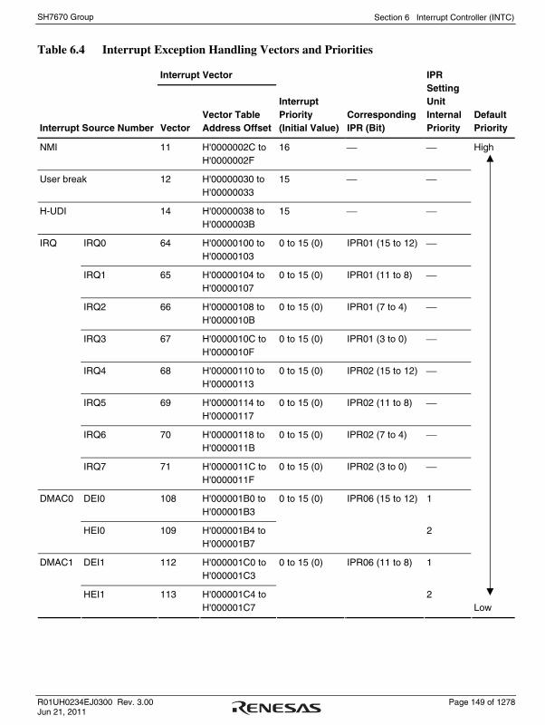
Section 6 Interrupt Controller (INTC)
R01UH0234EJ0300 Rev. 3.00 Page 149 of 1278 Jun 21, 2011
SH7670 Group
Table 6.4 Interrupt Exception Handling Vectors and Priorities
Interrupt Vector
Interrupt Source Number Vector Vector Table Address Offset
Interrupt Priority (Initial Value)
Corresponding IPR (Bit)
IPR Setting Unit Internal Priority
Default Priority
NMI 11 H'0000002C to H'0000002F
16 ⎯ ⎯ High
User break 12 H'00000030 to H'00000033
15 ⎯ ⎯
H-UDI 14 H'00000038 to H'0000003B
15 ⎯ ⎯
IRQ0 64 H'00000100 to H'00000103
0 to 15 (0) IPR01 (15 to 12) ⎯
IRQ1 65 H'00000104 to H'00000107
0 to 15 (0) IPR01 (11 to 8) ⎯
IRQ2 66 H'00000108 to H'0000010B
0 to 15 (0) IPR01 (7 to 4) ⎯
IRQ3 67 H'0000010C to H'0000010F
0 to 15 (0) IPR01 (3 to 0) ⎯
IRQ4 68 H'00000110 to H'00000113
0 to 15 (0) IPR02 (15 to 12) ⎯
IRQ5 69 H'00000114 to H'00000117
0 to 15 (0) IPR02 (11 to 8) ⎯
IRQ6 70 H'00000118 to H'0000011B
0 to 15 (0) IPR02 (7 to 4) ⎯
IRQ
IRQ7 71 H'0000011C to H'0000011F
0 to 15 (0) IPR02 (3 to 0) ⎯
DEI0 108 H'000001B0 to H'000001B3
1 DMAC0
HEI0 109 H'000001B4 to H'000001B7
0 to 15 (0) IPR06 (15 to 12)
2
DEI1 112 H'000001C0 to H'000001C3
1
DMAC1
HEI1 113 H'000001C4 to H'000001C7
0 to 15 (0) IPR06 (11 to 8)
2 Low

Section 6 Interrupt Controller (INTC)
Page 150 of 1278 R01UH0234EJ0300 Rev. 3.00 Jun 21, 2011
SH7670 Group
Interrupt Vector
Interrupt Source Number Vector Vector Table Address Offset
Interrupt Priority (Initial Value)
Corresponding IPR (Bit)
IPR Setting Unit Internal Priority
Default Priority
DEI2 116 H'000001D0 to H'000001D3
1 High DMAC2
HEI2 117 H'000001D4 to H'000001D7
0 to 15 (0) IPR06 (7 to 4)
2
DEI3 120 H'000001E0 to H'000001E3
1 DMAC3
HEI3 121 H'000001E4 to H'000001E7
0 to 15 (0) IPR06 (3 to 0)
2
DEI4 124 H'000001F0 to H'000001F3
1 DMAC4
HEI4 125 H'000001F4 to H'000001F7
0 to 15 (0) IPR07 (15 to 12)
2
DEI5 128 H'00000200 to H'00000203
1 DMAC5
HEI5 129 H'00000204 to H'00000207
0 to 15 (0) IPR07 (11 to 8)
2
DEI6 132 H'00000210 to H'00000213
1 DMAC6
HEI6 133 H'00000214 to H'00000217
0 to 15 (0) IPR07 (7 to 4)
2
DEI7 136 H'00000220 to H'00000223
1 DMAC7
HEI7 137 H'00000224 to H'00000227
0 to 15 (0) IPR07 (3 to 0)
2
USB USBI 140 H'00000230 to H'00000233
0 to 15 (0) IPR08 (15 to 12) ⎯
CMI0 142 H'00000238 to H'0000023B
0 to 15 (0) IPR08 (7 to 4) ⎯ CMT
CMI1 143 H'0000023C to H'0000023F
0 to 15 (0) IPR08 (3 to 0) ⎯
BSC CMI 144 H'00000240 to H'00000243
0 to 15 (0) IPR09 (15 to 12) ⎯
WDT ITI 145 H'00000244 to H'00000247
0 to 15 (0) IPR09 (11 to 8) ⎯ Low
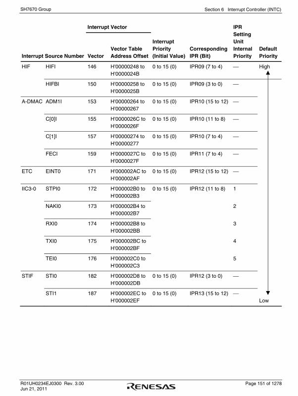
Section 6 Interrupt Controller (INTC)
R01UH0234EJ0300 Rev. 3.00 Page 151 of 1278 Jun 21, 2011
SH7670 Group
Interrupt Vector
Interrupt Source Number Vector Vector Table Address Offset
Interrupt Priority (Initial Value)
Corresponding IPR (Bit)
IPR Setting Unit Internal Priority
Default Priority
HIFI 146 H'00000248 to H'0000024B
0 to 15 (0) IPR09 (7 to 4) ⎯ High HIF
HIFBI 150 H'00000258 to H'0000025B
0 to 15 (0) IPR09 (3 to 0) ⎯
ADM1I 153 H'00000264 to H'00000267
0 to 15 (0) IPR10 (15 to 12) ⎯
C[0]I 155 H'0000026C to H'0000026F
0 to 15 (0) IPR10 (11 to 8) ⎯
C[1]I 157 H'00000274 to H'00000277
0 to 15 (0) IPR10 (7 to 4) ⎯
A-DMAC
FECI 159 H'0000027C to H'0000027F
0 to 15 (0) IPR11 (7 to 4) ⎯
ETC EINT0 171 H'000002AC to H'000002AF
0 to 15 (0) IPR12 (15 to 12) ⎯
STPI0 172 H'000002B0 to H'000002B3
1
NAKI0 173 H'000002B4 to H'000002B7
2
RXI0 174 H'000002B8 to H'000002BB
3
TXI0 175 H'000002BC to H'000002BF
4
IIC3-0
TEI0 176 H'000002C0 to H'000002C3
0 to 15 (0) IPR12 (11 to 8)
5
STIF STI0 182 H'000002D8 to H'000002DB
0 to 15 (0) IPR12 (3 to 0) ⎯
STI1 187 H'000002EC to H'000002EF
0 to 15 (0) IPR13 (15 to 12) ⎯ Low

Section 6 Interrupt Controller (INTC)
Page 152 of 1278 R01UH0234EJ0300 Rev. 3.00 Jun 21, 2011
SH7670 Group
Interrupt Vector
Interrupt Source Number Vector Vector Table Address Offset
Interrupt Priority (Initial Value)
Corresponding IPR (Bit)
IPR Setting Unit Internal Priority
Default Priority
BRI0 192 H'00000300 to H'00000303
1 High
ERI0 193 H'00000304 to H'00000307
2
RXI0 194 H'00000308 to H'0000030B
3
SCIF0
TXI0 195 H'0000030C to H'0000030F
0 to 15 (0) IPR13 (11 to 8)
4
BRI1 196 H'00000310 to H'00000313
1
ERI1 197 H'00000314 to H'00000317
2
RXI1 198 H'00000318 to H'0000031B
3
SCIF1
TXI1 199 H'0000031C to H'0000031F
0 to 15 (0) IPR13 (7 to 4)
4
BRI2 200 H'00000320 to H'00000323
1
ERI2 201 H'00000324 to H'00000327
2
RXI2 202 H'00000328 to H'0000032B
3
SCIF2
TXI2 203 H'0000032C to H'0000032F
0 to 15 (0) IPR13 (3 to 0)
4
SSI0 SSII0 214 H'00000358 to H'0000035B
0 to 15 (0) IPR14 (3 to 0) ⎯
SSI1 SSII1 215 H'0000035C to H'0000035F
0 to 15 (0) IPR15 (15 to 12) ⎯
SDII3 228 H'00000390 to H'00000393
1
SDII0 229 H'00000394 to H'00000397
2
SDIO
SDII1 230 H'00000398 to H'0000039B
0 to 15 (0) IPR16 (11 to 8)
3 Low

Section 6 Interrupt Controller (INTC)
R01UH0234EJ0300 Rev. 3.00 Page 153 of 1278 Jun 21, 2011
SH7670 Group
6.6 Operation
6.6.1 Interrupt Operation Sequence
The sequence of interrupt operations is described below. Figure 6.2 shows the operation flow.
1. The interrupt request sources send interrupt request signals to the interrupt controller.
2. The interrupt controller selects the highest-priority interrupt from the interrupt requests sent, following the priority levels set in interrupt priority registers 01, 02, and 06 to 16 (IPR01, IPR02, and IPR06 to IPR16). Lower priority interrupts are ignored*. If two of these interrupts have the same priority level or if multiple interrupts occur within a single IPR, the interrupt with the highest priority is selected, according to the default priority and IPR setting unit internal priority shown in table 6.4.
3. The priority level of the interrupt selected by the interrupt controller is compared with the interrupt level mask bits (I3 to I0) in the status register (SR) of the CPU. If the interrupt request priority level is equal to or less than the level set in bits I3 to I0, the interrupt request is ignored. If the interrupt request priority level is higher than the level in bits I3 to I0, the interrupt controller accepts the interrupt and sends an interrupt request signal to the CPU.
5. The CPU detects the interrupt request sent from the interrupt controller when the CPU decodes the instruction to be executed. Instead of executing the decoded instruction, the CPU starts interrupt exception handling (figure 6.4).
6. The interrupt exception service routine start address is fetched from the exception handling vector table corresponding to the accepted interrupt.
7. The status register (SR) is saved onto the stack, and the priority level of the accepted interrupt is copied to bits I3 to I0 in SR.
8. The program counter (PC) is saved onto the stack.
9. The CPU jumps to the fetched interrupt exception service routine start address and starts executing the program. The jump that occurs is not a delayed branch.
10. A high level is output from the IRQOUT pin. However, if the interrupt controller accepts an interrupt with a higher priority than the interrupt just being accepted, the IRQOUT pin holds low level.

Section 6 Interrupt Controller (INTC)
Page 154 of 1278 R01UH0234EJ0300 Rev. 3.00 Jun 21, 2011
SH7670 Group
Notes: The interrupt source flag should be cleared in the interrupt handler. After clearing the interrupt source flag, "time from occurrence of interrupt request until interrupt controller identifies priority, compares it with mask bits in SR, and sends interrupt request signal to CPU" shown in table 6.5 is required before the interrupt source sent to the CPU is actually cancelled. To ensure that an interrupt request that should have been cleared is not inadvertently accepted again, read the interrupt source flag after it has been cleared, and then execute an RTE instruction.
* Interrupt requests that are designated as edge-sensing are held pending until the interrupt requests are accepted. IRQ interrupts, however, can be cancelled by accessing the IRQ interrupt request register (IRQRR). For details, see section 6.4.4, IRQ Interrupts. Interrupts held pending due to edge-sensing are cleared by a power-on reset.

Section 6 Interrupt Controller (INTC)
R01UH0234EJ0300 Rev. 3.00 Page 155 of 1278 Jun 21, 2011
SH7670 Group
No
No
No
No
Yes
Yes
Yes
Yes
Yes
Yes
No
Yes
No Yes
Yes
No
No
No
No
Programexecution state
Interrupt?
NMI?
User break?
I3 to I0 ≤level 14?
Level 14interrupt?
Level 1interrupt?
I3 to I0 ≤level 13?
I3 to I0 =level 0?
H-UDIinterrupt?
Level 15interrupt?
IRQOUT = low
Save SR to stack
Save PC to stack
Copy accept-interruptlevel to I3 to I0
IRQOUT = high
Read exceptionhandling vector table
Branch to interruptexception service routine
Figure 6.2 Interrupt Operation Flow

Section 6 Interrupt Controller (INTC)
Page 156 of 1278 R01UH0234EJ0300 Rev. 3.00 Jun 21, 2011
SH7670 Group
6.6.2 Stack after Interrupt Exception Handling
Figure 6.3 shows the stack after interrupt exception handling.
Address
SP*24n – 8 PC*1
SR4n – 4
4n
32 bits
32 bits
Notes: 1. PC: Start address of the next instruction (return destination instruction) after the executed instruction 2. Always make sure that SP is a multiple of 4.
Figure 6.3 Stack after Interrupt Exception Handling

Section 6 Interrupt Controller (INTC)
R01UH0234EJ0300 Rev. 3.00 Page 157 of 1278 Jun 21, 2011
SH7670 Group
6.7 Interrupt Response Time
Table 6.5 lists the interrupt response time, which is the time from the occurrence of an interrupt request until the interrupt exception handling starts and fetching of the first instruction in the exception service routine begins. The interrupt processing operations differ in the cases when banking is disabled, when banking is enabled without register bank overflow, and when banking is enabled with register bank overflow. Figures 6.4 and 6.5 show examples of pipeline operation when banking is disabled. Figures 6.6 and 6.7 show examples of pipeline operation when banking is enabled without register bank overflow. Figures 6.8 and 6.9 show examples of pipeline operation when banking is enabled with register bank overflow.
Table 6.5 Interrupt Response Time
Number of States
Item NMI User Break H-UDI IRQ, PINT
Peripheral
Module
Remarks
Time from occurrence of interrupt
request until interrupt controller
identifies priority, compares it with
mask bits in SR, and sends interrupt
request signal to CPU
2 Icyc +
2 Bcyc +
1 Pcyc
3 Icyc 2 Icyc +
1 Pcyc
2 Icyc +
3 Bcyc +
1 Pcyc
2 Icyc +
1 Bcyc +
1 Pcyc
Min. 3 Icyc + m1 + m2 No register
banking Max. 4 Icyc + 2(m1 + m2) + m3
Min. is when the interrupt
wait time is zero.
Max. is when a higher-priority
interrupt request has
occurred during interrupt
exception handling.
Min. ⎯ 3 Icyc + m1 + m2 Register
banking
without
register
bank
overflow
Max. ⎯ 12 Icyc + m1 + m2
Min. is when the interrupt
wait time is zero.
Max. is when an interrupt
request has occurred during
execution of the RESBANK
instruction.
Min. ⎯ 3 Icyc + m1 + m2
Time from
input of
interrupt
request signal
to CPU until
sequence
currently being
executed is
completed,
interrupt
exception
handling starts,
and first
instruction in
interrupt
exception
service routine
is fetched
Register
banking
with register
bank
overflow
Max. ⎯ 3 Icyc + m1 + m2 + 19(m4)
Min. is when the interrupt
wait time is zero.
Max. is when an interrupt
request has occurred during
execution of the RESBANK
instruction.

Section 6 Interrupt Controller (INTC)
Page 158 of 1278 R01UH0234EJ0300 Rev. 3.00 Jun 21, 2011
SH7670 Group
Number of States
Item NMI User Break H-UDI IRQ, PINT
Peripheral
Module
Remarks
Min. 5 Icyc +
2 Bcyc +
1 Pcyc +
m1 + m2
6 Icyc +
m1 + m2
5 Icyc +
1 Pcyc +
m1 + m2
5 Icyc +
3 Bcyc +
1 Pcyc +
m1 + m2
5 Icyc +
1 Bcyc +
1 Pcyc +
m1 + m2
200-MHz operation*1*2:
0.040 to 0.110 μs
No register
banking
Max. 6 Icyc +
2 Bcyc +
1 Pcyc +
2(m1 + m2) +
m3
7 Icyc +
2(m1 + m2) +
m3
6 Icyc +
1 Pcyc +
2(m1 + m2) +
m3
6 Icyc +
3 Bcyc +
1 Pcyc +
2(m1 + m2) +
m3
6 Icyc +
1 Bcyc +
1 Pcyc +
2(m1 + m2) +
m3
200-MHz operation*1*2:
0.060 to 0.130 μs
Min. ⎯ ⎯ 5 Icyc +
1 Pcyc +
m1 + m2
5 Icyc +
3 Bcyc +
1 Pcyc +
m1 + m2
5 Icyc +
1 Bcyc +
1 Pcyc +
m1 + m2
200-MHz operation*1*2:
0.040 to 0.110 μs
Register
banking
without
register
bank
overflow Max. ⎯ ⎯ 14 Icyc +
1 Pcyc +
m1 + m2
14 Icyc +
3 Bcyc +
1 Pcyc +
m1 + m2
14 Icyc +
1 Bcyc +
1 Pcyc +
m1 + m2
200-MHz operation*1*2:
0.085 to 0.155 μs
Min. ⎯ ⎯ 5 Icyc +
1 Pcyc +
m1 + m2
5 Icyc +
3 Bcyc +
1 Pcyc +
m1 + m2
5 Icyc +
1 Bcyc +
1 Pcyc +
m1 + m2
200-MHz operation*1*2:
0.040 to 0.110 μs
Interrupt
response time
Register
banking
with register
bank
overflow Max. ⎯ ⎯ 5 Icyc +
1 Pcyc + m1 +
m2 + 19(m4)
5 Icyc +
3 Bcyc +
1 Pcyc + m1 +
m2 + 19(m4)
5 Icyc +
1 Bcyc +
1 Pcyc + m1 +
m2 + 19(m4)
200-MHz operation*1*2:
0.135 to 0.205 μs
Notes: m1 to m4 are the number of states needed for the following memory accesses.
m1: Vector address read (longword read) m2: SR save (longword write)
m3: PC save (longword write)
m4: Banked registers (R0 to R14, GBR, MACH, MACL, and PR) are restored from the stack.
1. In the case that m1 = m2 = m3 = m4 = 1 Icyc. 2. In the case that (Iφ, Bφ, Pφ) = (200 MHz, 66 MHz, 33 MHz).
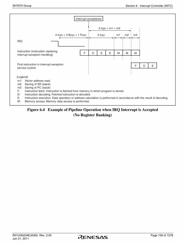
Section 6 Interrupt Controller (INTC)
R01UH0234EJ0300 Rev. 3.00 Page 159 of 1278 Jun 21, 2011
SH7670 Group
F
2 Icyc + 3 Bcyc + 1 Pcyc 3 Icyc m1 m2 m3
3 Icyc + m1 + m2
IRQ
Instruction (instruction replacing interrupt exception handling)
m1:m2:m3:F:D:E:M:
First instruction in interrupt exceptionservice routine
Interrupt acceptance
D E E M M M
F D E
[Legend]Vector address readSaving of SR (stack)Saving of PC (stack)Instruction fetch. Instruction is fetched from memory in which program is stored.Instruction decoding. Fetched instruction is decoded.Instruction execution. Data operation or address calculation is performed in accordance with the result of decoding.Memory access. Memory data access is performed.
Figure 6.4 Example of Pipeline Operation when IRQ Interrupt is Accepted (No Register Banking)

Section 6 Interrupt Controller (INTC)
Page 160 of 1278 R01UH0234EJ0300 Rev. 3.00 Jun 21, 2011
SH7670 Group
F
2 Icyc + 3 Bcyc + 1 Pcyc 1 Icyc + m1 + 2(m2) + m3
m1 m2 m3
3 Icyc + m1
IRQ
D E E M M M
D E E M M M
F D
F D
m1 m2
[Legend]m1:m2:m3:
Vector address readSaving of SR (stack)Saving of PC (stack)
Interrupt acceptance Multiple interrupt acceptance
First instruction in interrupt exceptionservice routine
First instruction in multiple interruptexception service routine
Figure 6.5 Example of Pipeline Operation for Multiple Interrupts (No Register Banking)
F
2 Icyc + 3 Bcyc + 1 Pcyc 3 Icyc m1 m2 m3
3 Icyc + m1 + m2
IRQ
D E E M M M E
F D E
[Legend]m1:m2:m3:
Vector address readSaving of SR (stack)Saving of PC (stack)
Interrupt acceptance
First instruction in interrupt exceptionservice routine
Instruction (instruction replacinginterrupt exception handling)
Figure 6.6 Example of Pipeline Operation when IRQ Interrupt is Accepted (Register Banking without Register Bank Overflow)

Section 6 Interrupt Controller (INTC)
R01UH0234EJ0300 Rev. 3.00 Page 161 of 1278 Jun 21, 2011
SH7670 Group
F
2 Icyc + 3 Bcyc + 1 Pcyc 3 Icyc + m1 + m2
m1 m2 m3
9 Icyc
IRQ
RESBANK instruction D E E E E E E E E E
D E E M M M E
F D
[Legend]
m1:m2:m3:
Vector address readSaving of SR (stack)Saving of PC (stack)
Interrupt acceptance
First instruction in interruptexception service routine
Instruction (instruction replacinginterrupt exception handling)
Figure 6.7 Example of Pipeline Operation when Interrupt is Accepted during RESBANK Instruction Execution (Register Banking without Register Bank Overflow)
F
2 Icyc + 3 Bcyc + 1 Pcyc 3 Icyc m1 m2 m3
3 Icyc + m1 + m2
IRQ
D E E M M MM
F D
[Legend]m1:m2:m3:
Vector address readSaving of SR (stack)Saving of PC (stack)
Interrupt acceptance
First instruction in interrupt exceptionservice routine
Instruction (instruction replacinginterrupt exception handling)
... ...
...
Figure 6.8 Example of Pipeline Operation when IRQ Interrupt is Accepted (Register Banking with Register Bank Overflow)

Section 6 Interrupt Controller (INTC)
Page 162 of 1278 R01UH0234EJ0300 Rev. 3.00 Jun 21, 2011
SH7670 Group
F
2 Icyc + 3 Bcyc + 1 Pcyc 1 Icyc + m1 + m2 + 2(m4)
m1 m2 m3
2 Icyc + 17(m4)
IRQ
RESBANK instruction D E M M M M M M W
D E E M M M
F D
m4 m4
[Legend]
m1:m2:m3:m4:
Vector address readSaving of SR (stack)Saving of PC (stack)Restoration of banked registers
Interrupt acceptance
First instruction in interruptexception service routine
Instruction (instruction replacinginterrupt exception handling)
...
...
...
Figure 6.9 Example of Pipeline Operation when Interrupt is Accepted during RESBANK Instruction Execution (Register Banking with Register Bank Overflow)
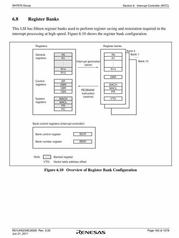
Section 6 Interrupt Controller (INTC)
R01UH0234EJ0300 Rev. 3.00 Page 163 of 1278 Jun 21, 2011
SH7670 Group
6.8 Register Banks
This LSI has fifteen register banks used to perform register saving and restoration required in the interrupt processing at high speed. Figure 6.10 shows the register bank configuration.
General registers
Bank control register
Bank number register
Bank control registers (interrupt controller)
Banked register
Vector table address offset
Note:
Interrupt generated(save)
RESBANK instruction(restore)
Registers Register banks
Bank 0Bank 1
....
Bank 14
R0R1
::
R14R15
SRGBRVBRTBR
MACHMACL
PRPC
Control registers
System registers
R0R1
::
R14
GBR
VTO
VTO:
IBCR
IBNR
MACHMACL
PR
:
Figure 6.10 Overview of Register Bank Configuration

Section 6 Interrupt Controller (INTC)
Page 164 of 1278 R01UH0234EJ0300 Rev. 3.00 Jun 21, 2011
SH7670 Group
6.8.1 Banked Register and Input/Output of Banks
(1) Banked Register
The contents of the general registers (R0 to R14), global base register (GBR), multiply and accumulate registers (MACH and MACL), and procedure register (PR), and the vector table address offset are banked.
(2) Input/Output of Banks
This LSI has fifteen register banks, bank 0 to bank 14. Register banks are stacked in first-in last-out (FILO) sequence. Saving takes place in order, beginning from bank 0, and restoration takes place in the reverse order, beginning from the last bank saved to.
6.8.2 Bank Save and Restore Operations
(1) Saving to Bank
Figure 6.11 shows register bank save operations. The following operations are performed when an interrupt for which usage of register banks is allowed is accepted by the CPU:
a. Assume that the bank number bit value in the bank number register (IBNR), BN, is i before the interrupt is generated.
b. The contents of registers R0 to R14, GBR, MACH, MACL, and PR, and the interrupt vector table address offset (VTO) of the accepted interrupt are saved in the bank indicated by BN, bank i.
c. The BN value is incremented by 1.
Bank 0
Register banks Registers
Bank 1::
::
Bank iBank i + 1
Bank 14
+1
(a)
(c)
(b)
BN GBRMACHMACL
PR
VTO
R0 to R14
Figure 6.11 Bank Save Operations

Section 6 Interrupt Controller (INTC)
R01UH0234EJ0300 Rev. 3.00 Page 165 of 1278 Jun 21, 2011
SH7670 Group
Figure 6.12 shows the timing for saving to a register bank. Saving to a register bank takes place between the start of interrupt exception handling and the start of fetching the first instruction in the interrupt exception service routine.
F
2 Icyc + 3 Bcyc + 1 Pcyc 3 Icyc m1 m2 m3
3 Icyc + m1 + m2
IRQ
(1) VTO, PR, GBR, MACL
(2) R12, R13, R14, MACH
(3) R8, R9, R10, R11
(4) R4, R5, R6, R7
(5) R0, R1, R2, R3Overrun fetchSaved to bank
D E E M M M E
F
F D E
[Legend]m1:m2:m3:
Vector address readSaving of SR (stack)Saving of PC (stack)
First instruction in interrupt exceptionservice routine
Instruction (instruction replacinginterrupt exception handling)
Figure 6.12 Bank Save Timing
(2) Restoration from Bank
The RESBANK (restore from register bank) instruction is used to restore data saved in a register bank. After restoring data from the register banks with the RESBANK instruction at the end of the interrupt exception service routine, execute the RTE instruction to return from interrupt exception service routine.
Section 6 Interrupt Controller (INTC)
Page 166 of 1278 R01UH0234EJ0300 Rev. 3.00 Jun 21, 2011
SH7670 Group
6.8.3 Save and Restore Operations after Saving to All Banks
If an interrupt occurs and usage of the register banks is enabled for the interrupt accepted by the CPU in a state where saving has been performed to all register banks, automatic saving to the stack is performed instead of register bank saving if the BOVE bit in the bank number register (IBNR) is cleared to 0. If the BOVE bit in IBNR is set to 1, register bank overflow exception occurs and data is not saved to the stack.
Save and restore operations when using the stack are as follows:
(1) Saving to Stack
1. The status register (SR) and program counter (PC) are saved to the stack during interrupt exception handling.
2. The contents of the banked registers (R0 to R14, GBR, MACH, MACL, and PR) are saved to the stack. The registers are saved to the stack in the order of MACL, MACH, GBR, PR, R14, R13, …, R1, and R0.
3. The register bank overflow bit (BO) in SR is set to 1.
4. The bank number bit (BN) value in the bank number register (IBNR) remains set to the maximum value of 15.
(2) Restoration from Stack
When the RESBANK (restore from register bank) instruction is executed with the register bank overflow bit (BO) in SR set to 1, the CPU operates as follows:
1. The contents of the banked registers (R0 to R14, GBR, MACH, MACL, and PR) are restored from the stack. The registers are restored from the stack in the order of R0, R1, …, R13, R14, PR, GBR, MACH, and MACL.
2. The bank number bit (BN) value in the bank number register (IBNR) remains set to the maximum value of 15.

Section 6 Interrupt Controller (INTC)
R01UH0234EJ0300 Rev. 3.00 Page 167 of 1278 Jun 21, 2011
SH7670 Group
6.8.4 Register Bank Exception
There are two register bank exceptions (register bank errors): register bank overflow and register bank underflow.
(1) Register Bank Overflow
This exception occurs if, after data has been saved to all of the register banks, an interrupt for which register bank use is allowed is accepted by the CPU, and the BOVE bit in the bank number register (IBNR) is set to 1. In this case, the bank number bit (BN) value in the bank number register (IBNR) remains set to the bank count of 15 and saving is not performed to the register bank.
(2) Register Bank Underflow
This exception occurs if the RESBANK (restore from register bank) instruction is executed when no data has been saved to the register banks. In this case, the values of R0 to R14, GBR, MACH, MACL, and PR do not change. In addition, the bank number bit (BN) value in the bank number register (IBNR) remains set to 0.
6.8.5 Register Bank Error Exception Handling
When a register bank error occurs, register bank error exception handling starts. When this happens, the CPU operates as follows:
1. The exception service routine start address which corresponds to the register bank error that occurred is fetched from the exception handling vector table.
2. The status register (SR) is saved to the stack.
3. The program counter (PC) is saved to the stack. The PC value saved is the start address of the instruction to be executed after the last executed instruction for a register bank overflow, and the start address of the executed RESBANK instruction for a register bank underflow. To prevent multiple interrupts from occurring at a register bank overflow, the interrupt priority level that caused the register bank overflow is written to the interrupt mask level bits (I3 to I0) of the status register (SR).
4. Program execution starts from the exception service routine start address.

Section 6 Interrupt Controller (INTC)
Page 168 of 1278 R01UH0234EJ0300 Rev. 3.00 Jun 21, 2011
SH7670 Group
6.9 Data Transfer with Interrupt Request Signals
Interrupt request signals can be used to activate the DMAC and transfer data.
Interrupt sources that are designated to activate the DMAC are masked without being input to the INTC. The mask condition is as follows:
Mask condition = DME • (DE0 • interrupt source select 0 + DE1 • interrupt source select 1 + DE2 • interrupt source select 2 + DE3 • interrupt source select 3 + DE4 • interrupt source select 4 + DE5 • interrupt source select 5 + DE6 • interrupt source select 6 + DE7 • interrupt source select 7)
Figure 6.13 shows a block diagram of interrupt control.
Here, DME is bit 0 in DMAOR of the DMAC, and DEn (n = 0 to 7) is bit 0 in CHCR0 to CHCR7 of the DMAC. For details, see section 8, Direct Memory Access Controller (DMAC).
DMAC
INTC CPUCPU interrupt request
Interrupt source
Interrupt source (not specified as DMAC activating source)
Interrupt source flag clearing(by DMAC)
Figure 6.13 Interrupt Control Block Diagram

Section 6 Interrupt Controller (INTC)
R01UH0234EJ0300 Rev. 3.00 Page 169 of 1278 Jun 21, 2011
SH7670 Group
6.9.1 Handling Interrupt Request Signals as Sources for CPU Interrupt but Not DMAC
Activating
1. Do not select DMAC activating sources or clear the DME bit to 0. If, DMAC activating sources are selected, clear the DE bit to 0 for the relevant channel of the DMAC.
2. When interrupts occur, interrupt requests are sent to the CPU.
3. The CPU clears the interrupt source and performs the necessary processing in the interrupt exception service routine.
6.9.2 Handling Interrupt Request Signals as Sources for Activating DMAC but Not CPU
Interrupt
1. Select DMAC activating sources and set both the DE and DME bits to 1. This masks CPU interrupt sources regardless of the interrupt priority register settings.
2. Activating sources are applied to the DMAC when interrupts occur.
3. The DMAC clears the interrupt sources when starting transfer.

Section 6 Interrupt Controller (INTC)
Page 170 of 1278 R01UH0234EJ0300 Rev. 3.00 Jun 21, 2011
SH7670 Group
6.10 Usage Note
6.10.1 Timing to Clear an Interrupt Source
The interrupt source flags should be cleared in the interrupt exception service routine. After clearing the interrupt source flag, "time from occurrence of interrupt request until interrupt controller identifies priority, compares it with mask bits in SR, and sends interrupt request signal to CPU" shown in table 6.5 is required before the interrupt source sent to the CPU is actually cancelled. To ensure that an interrupt request that should have been cleared is not inadvertently accepted again, read the interrupt source flag after it has been cleared, and then execute an RTE instruction.

Section 7 Bus State Controller (BSC)
R01UH0234EJ0300 Rev. 3.00 Page 171 of 1278 Jun 21, 2011
SH7670 Group
Section 7 Bus State Controller (BSC)
The bus state controller (BSC) outputs control signals for various types of memory and external devices that are connected to the external address space. BSC functions enable this LSI to connect directly with SRAM, SDRAM, and other memory storage devices, and external devices.
7.1 Features
1. External address space
⎯ A maximum of 64 Mbytes for each of areas CS0 and CS3 to CS6.
⎯ Can specify the normal space interface, SRAM interface with byte selection, SDRAM, and PCMCIA interface for each address space.
⎯ Can select the data bus width (8, 16, or 32 bits) for each address space.
⎯ Controls insertion of wait cycles for each address space.
⎯ Controls insertion of wait cycles for each read access and write access.
⎯ Can set independent idle cycles during the continuous access for five cases: read-write (in same space/different spaces), read-read (in same space/different spaces), the first cycle is a write access.
⎯ For area 0, only big endian is supported.
2. Normal space interface
⎯ Supports the interface that can directly connect to the SRAM.
3. SDRAM interface
⎯ Multiplex output for row address/column address.
⎯ Efficient access by single read/single write.
⎯ High-speed access in bank-active mode.
⎯ Supports an auto-refresh and self-refresh.
⎯ Supports power-down modes.
⎯ Issues MRS and EMRS commands.
4. PCMCIA direct interface
⎯ Supports the IC memory card and I/O card interface defined in JEIDA specifications Ver. 4.2 (PCMCIA2.1 Rev. 2.1).
⎯ Wait-cycle insertion controllable by program.
5. SRAM interface with byte selection
⎯ Can connect directly to a SRAM with byte selection.

Section 7 Bus State Controller (BSC)
Page 172 of 1278 R01UH0234EJ0300 Rev. 3.00 Jun 21, 2011
SH7670 Group
6. Refresh function
⎯ Supports the auto-refresh and self-refresh functions.
⎯ Specifies the refresh interval using the refresh counter and clock selection.
⎯ Can execute concentrated refresh by specifying the refresh counts (1, 2, 4, 6, or 8).
7. Usage as interval timer for refresh counter
⎯ Generates an interrupt request at compare match.

Section 7 Bus State Controller (BSC)
R01UH0234EJ0300 Rev. 3.00 Page 173 of 1278 Jun 21, 2011
SH7670 Group
Figure 7.1 shows a block diagram of the BSC.
CMNCR
CS0WCR
CS7WCR
CS0BCR
CS7BCR
SDCR
RTCSR
RTCNT
RTCOR
Comparator
Bus mastership controller
Wait controller
Area controller
Inte
rnal
bus
Memory controller
Refresh controller
[Legend]
Mod
ule
bus
BSC
CS0 to CS7
REFOUT
WAIT
MD
A25 to A0,D31 to D0
BACK
BREQ
BS, RD/WR, RD, WE3 to WE0, RASU, RASL, CASU, CASL
CKE, DQMxx, AH,FRAME, IOIS16, CE2A, CE2B
CMNCR: CSnWCR: CSnBCR: SDCR: RTCSR: RTCNT: RTCOR:
Common control registerCSn space wait control register (n = 0 to 7)CSn space bus control register (n = 0 to 7)SDRAM control registerRefresh timer control/status registerRefresh timer counterRefresh time constant register
. . .
. . .. . .
. . .. . .
Figure 7.1 Block Diagram of BSC

Section 7 Bus State Controller (BSC)
Page 174 of 1278 R01UH0234EJ0300 Rev. 3.00 Jun 21, 2011
SH7670 Group
7.2 Input/Output Pins
Table 7.1 shows the pin configuration of the BSC.
Table 7.1 Pin Configuration
Name I/O Function
A25 to A0 Output Address bus
D31 to D0 I/O Data bus
BS Output Bus cycle start
CS0, CS3, CS4 Output Chip select
CS5/CE1A, CS6/CE1B
Output Chip select
Function as PCMCIA card select signals for D7 to D0 when PCMCIA is used.
CE2A, CE2B Output Function as PCMCIA card select signals for D15 to D8.
RD/WR Output Read/write
Connects to WE pins when SDRAM or SRAM with byte selection is connected.
RD Output Read pulse signal (read data output enable signal)
Functions as a strobe signal for indicating memory read cycles when PCMCIA is used.
WE3/DQMUU/ ICIOWR
Output Indicates that D31 to D24 are being written to.
Connected to the byte select signal when a SRAM with byte selection is connected.
Functions as the select signals for D31 to D24 when SDRAM is connected.
Functions as a strobe signal for indicating I/O write cycles when PCMCIA is used.
WE2/DQMUL/ ICIORD
Output Indicates that D23 to D16 are being written to.
Connected to the byte select signal when a SRAM with byte selection is connected.
Functions as the select signals for D23 to D16 when SDRAM is connected.
Functions as a strobe signal for indicating I/O read cycles when PCMCIA is used.
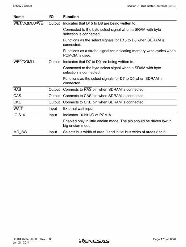
Section 7 Bus State Controller (BSC)
R01UH0234EJ0300 Rev. 3.00 Page 175 of 1278 Jun 21, 2011
SH7670 Group
Name I/O Function
WE1/DQMLU/WE Output Indicates that D15 to D8 are being written to.
Connected to the byte select signal when a SRAM with byte selection is connected.
Functions as the select signals for D15 to D8 when SDRAM is connected.
Functions as a strobe signal for indicating memory write cycles when PCMCIA is used.
WE0/DQMLL Output Indicates that D7 to D0 are being written to.
Connected to the byte select signal when a SRAM with byte selection is connected.
Functions as the select signals for D7 to D0 when SDRAM is connected.
RAS Output Connects to RAS pin when SDRAM is connected.
CAS Output Connects to CAS pin when SDRAM is connected.
CKE Output Connects to CKE pin when SDRAM is connected.
WAIT Input External wait input
IOIS16 Input Indicates 16-bit I/O of PCMIA.
Enabled only in little endian mode. The pin should be driven low in big endian mode.
MD_BW Input Selects bus width of area 0 and initial bus width of areas 3 to 6.
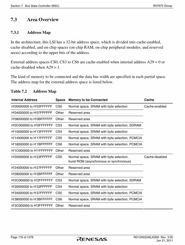
Section 7 Bus State Controller (BSC)
Page 176 of 1278 R01UH0234EJ0300 Rev. 3.00 Jun 21, 2011
SH7670 Group
7.3 Area Overview
7.3.1 Address Map
In the architecture, this LSI has a 32-bit address space, which is divided into cache-enabled, cache-disabled, and on-chip spaces (on-chip RAM, on-chip peripheral modules, and reserved areas) according to the upper bits of the address.
External address spaces CS0, CS3 to CS6 are cache-enabled when internal address A29 = 0 or cache-disabled when A29 = 1.
The kind of memory to be connected and the data bus width are specified in each partial space. The address map for the external address space is listed below.
Table 7.2 Address Map
Internal Address Space Memory to be Connected Cache
H'00000000 to H'03FFFFFF CS0 Normal space, SRAM with byte selection
H'04000000 to H'07FFFFFF Other Reserved area
H'08000000 to H'0BFFFFFF Other Reserved area
H'0C000000 to H'0FFFFFFF CS3 Normal space, SRAM with byte selection, SDRAM
H'10000000 to H'13FFFFFF CS4 Normal space, SRAM with byte selection
H'14000000 to H'17FFFFFF CS5 Normal space, SRAM with byte selection, PCMCIA
H'18000000 to H'1BFFFFFF CS6 Normal space, SRAM with byte selection, PCMCIA
H'1C000000 to H'1FFFFFFF Other Reserved area
Cache-enabled
H'20000000 to H'23FFFFFF CS0 Normal space, SRAM with byte selection, burst ROM (asynchronous or synchronous)
H'24000000 to H'27FFFFFF Other Reserved area
H'28000000 to H'2BFFFFFF Other Reserved area
H'2C000000 to H'2FFFFFFF CS3 Normal space, SRAM with byte selection, SDRAM
H'30000000 to H'33FFFFFF CS4 Normal space, SRAM with byte selection
H'34000000 to H'37FFFFFF CS5 Normal space, SRAM with byte selection, PCMCIA
H'38000000 to H'3BFFFFFF CS6 Normal space, SRAM with byte selection, PCMCIA
H'3C000000 to H'3FFFFFFF Other Reserved area
Cache-disabled
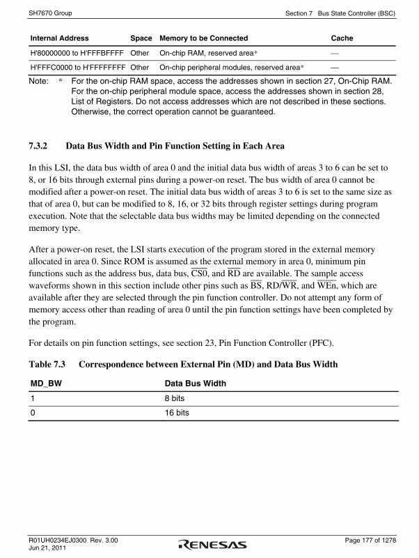
Section 7 Bus State Controller (BSC)
R01UH0234EJ0300 Rev. 3.00 Page 177 of 1278 Jun 21, 2011
SH7670 Group
Internal Address Space Memory to be Connected Cache
H'80000000 to H'FFFBFFFF Other On-chip RAM, reserved area* ⎯
H'FFFC0000 to H'FFFFFFFF Other On-chip peripheral modules, reserved area* ⎯
Note: * For the on-chip RAM space, access the addresses shown in section 27, On-Chip RAM. For the on-chip peripheral module space, access the addresses shown in section 28, List of Registers. Do not access addresses which are not described in these sections. Otherwise, the correct operation cannot be guaranteed.
7.3.2 Data Bus Width and Pin Function Setting in Each Area
In this LSI, the data bus width of area 0 and the initial data bus width of areas 3 to 6 can be set to 8, or 16 bits through external pins during a power-on reset. The bus width of area 0 cannot be modified after a power-on reset. The initial data bus width of areas 3 to 6 is set to the same size as that of area 0, but can be modified to 8, 16, or 32 bits through register settings during program execution. Note that the selectable data bus widths may be limited depending on the connected memory type.
After a power-on reset, the LSI starts execution of the program stored in the external memory allocated in area 0. Since ROM is assumed as the external memory in area 0, minimum pin functions such as the address bus, data bus, CS0, and RD are available. The sample access waveforms shown in this section include other pins such as BS, RD/WR, and WEn, which are available after they are selected through the pin function controller. Do not attempt any form of memory access other than reading of area 0 until the pin function settings have been completed by the program.
For details on pin function settings, see section 23, Pin Function Controller (PFC).
Table 7.3 Correspondence between External Pin (MD) and Data Bus Width
MD_BW Data Bus Width
1 8 bits
0 16 bits

Section 7 Bus State Controller (BSC)
Page 178 of 1278 R01UH0234EJ0300 Rev. 3.00 Jun 21, 2011
SH7670 Group
7.4 Register Descriptions
The BSC has the following registers.
Do not access spaces other than area 0 until settings of the connected memory interface are completed.
Table 7.4 Register Configuration
Register Name Abbreviation R/W Initial Value Address Access Size
Common control register CMNCR R/W H'00001010 H'FFFC0000 32
CS0 space bus control register CS0BCR R/W H'36DB0200* H'FFFC0004 32
CS3 space bus control register CS3BCR R/W H'36DB0200* H'FFFC0010 32
CS4 space bus control register CS4BCR R/W H'36DB0200* H'FFFC0014 32
CS5 space bus control register CS5BCR R/W H'36DB0200* H'FFFC0018 32
CS6 space bus control register CS6BCR R/W H'36DB0200* H'FFFC001C 32
CS0 space wait control register CS0WCR R/W H'00000500 H'FFFC0028 32
CS3 space wait control register CS3WCR R/W H'00000500 H'FFFC0034 32
CS4 space wait control register CS4WCR R/W H'00000500 H'FFFC0038 32
CS5 space wait control register CS5WCR R/W H'00000500 H'FFFC003C 32
CS6 space wait control register CS6WCR R/W H'00000500 H'FFFC0040 32
SDRAM control register SDCR R/W H'00000000 H'FFFC004C 32
Refresh timer control/status register RTCSR R/W H'00000000 H'FFFC0050 32
Refresh timer counter RTCNT R/W H'00000000 H'FFFC0054 32
Refresh time constant register RTCOR R/W H'00000000 H'FFFC0058 32
Internal bus master bus priority register
IBMPR R/W H'12300000 H'FFFC1818 32
Notes: * This is an initial value when this LSI is started by the external pin (MD_BW) with the bus width set to 8 bits. The initial value will be H'36DB0400 when the bus width is set to 16 bits.
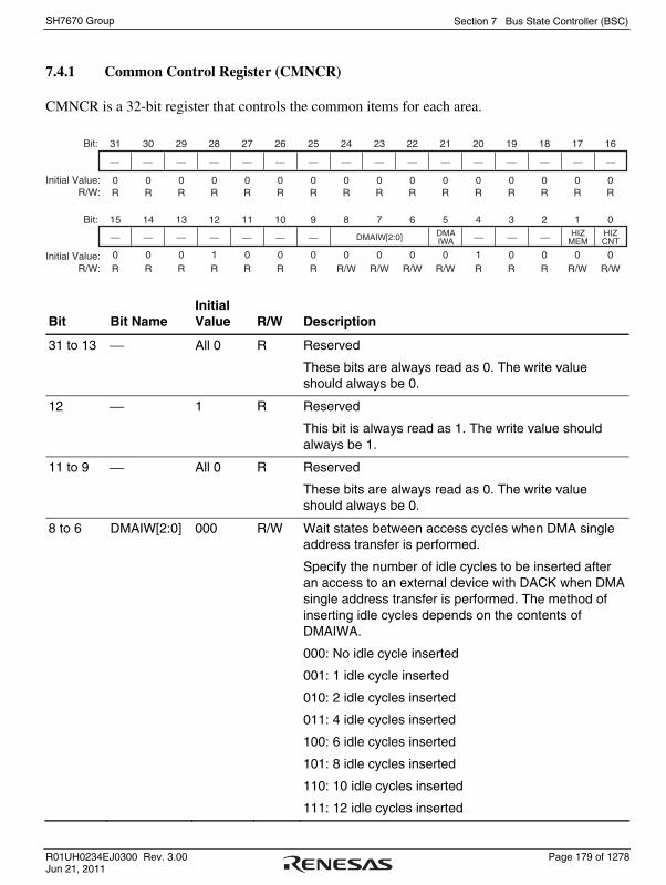
Section 7 Bus State Controller (BSC)
R01UH0234EJ0300 Rev. 3.00 Page 179 of 1278 Jun 21, 2011
SH7670 Group
7.4.1 Common Control Register (CMNCR)
CMNCR is a 32-bit register that controls the common items for each area.
31 30 29 28 27 26 25 24 23 22 21 20 19 18 17 16Bit:
Initial Value:R/W:
Bit:
Initial Value:R/W:
15 14 13 12 11 10 9 8 7 6 5 4 3 2 1 0
0 0 0 0 0 0 0 0 0 0 0 0 0 0 0 0R R R R R R R R R R R R R R R R
0 0 0 1 0 0 0 0 0 0 0 1 0 0 0 0R R R R R R R R/W R/W R/W R/W R R R R/W R/W
⎯ ⎯ ⎯ ⎯ ⎯ ⎯ ⎯
⎯ ⎯ ⎯
⎯ ⎯ ⎯ ⎯ ⎯ ⎯ ⎯ ⎯ ⎯
⎯ ⎯ ⎯ ⎯ DMAIW[2:0] DMAIWA ⎯ ⎯ ⎯ HIZ
MEMHIZCNT
Bit Bit Name Initial Value R/W Description
31 to 13 ⎯ All 0 R Reserved
These bits are always read as 0. The write value should always be 0.
12 ⎯ 1 R Reserved
This bit is always read as 1. The write value should always be 1.
11 to 9 ⎯ All 0 R Reserved
These bits are always read as 0. The write value should always be 0.
8 to 6 DMAIW[2:0] 000 R/W Wait states between access cycles when DMA single address transfer is performed.
Specify the number of idle cycles to be inserted after an access to an external device with DACK when DMA single address transfer is performed. The method of inserting idle cycles depends on the contents of DMAIWA.
000: No idle cycle inserted
001: 1 idle cycle inserted
010: 2 idle cycles inserted
011: 4 idle cycles inserted
100: 6 idle cycles inserted
101: 8 idle cycles inserted
110: 10 idle cycles inserted
111: 12 idle cycles inserted
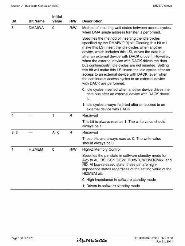
Section 7 Bus State Controller (BSC)
Page 180 of 1278 R01UH0234EJ0300 Rev. 3.00 Jun 21, 2011
SH7670 Group
Bit Bit Name Initial Value R/W Description
5 DMAIWA 0 R/W Method of inserting wait states between access cycles when DMA single address transfer is performed.
Specifies the method of inserting the idle cycles specified by the DMAIW[2:0] bit. Clearing this bit will make this LSI insert the idle cycles when another device, which includes this LSI, drives the data bus after an external device with DACK drove it. However, when the external device with DACK drives the data bus continuously, idle cycles are not inserted. Setting this bit will make this LSI insert the idle cycles after an access to an external device with DACK, even when the continuous access cycles to an external device with DACK are performed.
0: Idle cycles inserted when another device drives the data bus after an external device with DACK drove it.
1: Idle cycles always inserted after an access to an external device with DACK
4 ⎯ 1 R Reserved
This bit is always read as 1. The write value should always be 1.
3, 2 ⎯ All 0 R Reserved
These bits are always read as 0. The write value should always be 0.
1 HIZMEM 0 R/W High-Z Memory Control
Specifies the pin state in software standby mode for A25 to A0, BS, CSn, CE2x, RD/WR, WEn/DQMxx, and RD. At bus-released state, these pin are high-impedance states regardless of the setting value of the HIZMEM bit.
0: High impedance in software standby mode
1: Driven in software standby mode

Section 7 Bus State Controller (BSC)
R01UH0234EJ0300 Rev. 3.00 Page 181 of 1278 Jun 21, 2011
SH7670 Group
Bit Bit Name Initial Value R/W Description
0 HIZCNT* 0 R/W High-Z Control
Specifies the state of CKE, RAS, and CAS in software standby mode.
0: High impedance in software standby mode
1: Driven in software standby mode
Note: * For High-Z control of CKIO, see section 9, Clock Pulse Generator (CPG).
7.4.2 CSn Space Bus Control Register (CSnBCR) (n = 0, 3 to 6)
CSnBCR is a 32-bit readable/writable register that specifies the function of each area, the number of idle cycles between bus cycles, and the bus width.
Do not access external memory other than area 0 until CSnBCR initial setting is completed.
Idle cycles may be inserted even when they are not specified. For details, see section 7.5.8, Wait between Access Cycles.
31 30 29 28 27 26 25 24 23 22 21 20 19 18 17 16
15 14 13 12 11 10 9 8 7 6 5 4 3 2 1 0
0 0 1 1 0 1 1 0 1 1 0 1 1 0 1 1R R/W R/W R/W R/W R/W R/W R/W R/W R/W R/W R/W R/W R/W R/W R/W
0 0 0 0 0 1* 1* 0 0 0 0 0 0 0 0 0R R/W R/W R/W R/W R/W R/W R R R R R R R R R
Bit:
Initial value:R/W:
Bit:
Initial value:R/W:
Note: CSnBCR samples the external pin (MD) that specify the bus width at power-on reset.*
- IWW[2:0] IWRWD[2:0] IWRWS[2:0] IWRRD[2:0] IWRRS[2:0]
- TYPE[2:0] ENDIAN BSZ[1:0] - - - - - - - - -
Bit Bit Name Initial Value R/W Description
31 ⎯ 0 R Reserved This bit is always read as 0. The write value should always be 0.

Section 7 Bus State Controller (BSC)
Page 182 of 1278 R01UH0234EJ0300 Rev. 3.00 Jun 21, 2011
SH7670 Group
Bit Bit Name Initial Value R/W Description
30 to 28 IWW[2:0] 011 R/W Idle Cycles between Write-Read Cycles and Write-Write Cycles
These bits specify the number of idle cycles to be inserted after the access to a memory that is connected to the space. The target access cycles are the write-read cycle and write-write cycle.
000: No idle cycle inserted
001: 1 idle cycle inserted
010: 2 idle cycles inserted
011: 4 idle cycles inserted
100: 6 idle cycles inserted
101: 8 idle cycles inserted
110: 10 idle cycles inserted
111: 12 idle cycles inserted
27 to 25 IWRWD[2:0] 011 R/W Idle Cycles for Another Space Read-Write
Specify the number of idle cycles to be inserted after the access to a memory that is connected to the space. The target access cycle is a read-write one in which continuous access cycles switch between different spaces.
000: No idle cycle inserted
001: 1 idle cycle inserted
010: 2 idle cycles inserted
011: 4 idle cycles inserted
100: 6 idle cycles inserted
101: 8 idle cycles inserted
110: 10 idle cycles inserted
111: 12 idle cycles inserted

Section 7 Bus State Controller (BSC)
R01UH0234EJ0300 Rev. 3.00 Page 183 of 1278 Jun 21, 2011
SH7670 Group
Bit Bit Name Initial Value R/W Description
24 to 22 IWRWS[2:0] 011 R/W Idle Cycles for Read-Write in the Same Space
Specify the number of idle cycles to be inserted after the access to a memory that is connected to the space. The target cycle is a read-write cycle of which continuous access cycles are for the same space.
000: No idle cycle inserted
001: 1 idle cycle inserted
010: 2 idle cycles inserted
011: 4 idle cycles inserted
100: 6 idle cycles inserted
101: 8 idle cycles inserted
110: 10 idle cycles inserted
111: 12 idle cycles inserted
21 to 19 IWRRD[2:0] 011 R/W Idle Cycles for Read-Read in Another Space
Specify the number of idle cycles to be inserted after the access to a memory that is connected to the space. The target cycle is a read-read cycle of which continuous access cycles switch between different space.
000: No idle cycle inserted
001: 1 idle cycle inserted
010: 2 idle cycles inserted
011: 4 idle cycles inserted
100: 6 idle cycles inserted
101: 8 idle cycles inserted
110: 10 idle cycles inserted
111: 12 idle cycles inserted

Section 7 Bus State Controller (BSC)
Page 184 of 1278 R01UH0234EJ0300 Rev. 3.00 Jun 21, 2011
SH7670 Group
Bit Bit Name Initial Value R/W Description
18 to 16 IWRRS[2:0] 011 R/W Idle Cycles for Read-Read in the Same Space
Specify the number of idle cycles to be inserted after the access to a memory that is connected to the space. The target cycle is a read-read cycle of which continuous access cycles are for the same space.
000: No idle cycle inserted
001: 1 idle cycle inserted
010: 2 idle cycles inserted
011: 4 idle cycles inserted
100: 6 idle cycles inserted
101: 8 idle cycles inserted
110: 10 idle cycles inserted
111: 12 idle cycles inserted
15 ⎯ 0 R Reserved
This bit is always read as 0. The write value should always be 0.
14 to 12 TYPE[2:0] 000 R/W Specify the type of memory connected to a space.
000: Normal space
001: Setting prohibited
010: Setting prohibited
011: SRAM with byte selection
100: SDRAM
101: PCMCIA
110: Setting prohibited
111: Setting prohibited
For details for memory type in each area, see table 7.2.
11 ENDIAN 0 R/W Endian Setting
Specifies the arrangement of data in a space.
0: Arranged in big endian
1: Arranged in little endian
Note: Area 0 cannot be set to little endian mode. In the case of area 0, this bit is always read as 0, and the write value should always be 0.
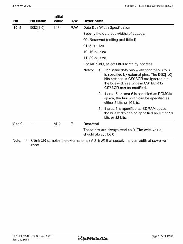
Section 7 Bus State Controller (BSC)
R01UH0234EJ0300 Rev. 3.00 Page 185 of 1278 Jun 21, 2011
SH7670 Group
Bit Bit Name Initial Value R/W Description
10, 9 BSZ[1:0] 11* R/W Data Bus Width Specification
Specify the data bus widths of spaces.
00: Reserved (setting prohibited)
01: 8-bit size
10: 16-bit size
11: 32-bit size
For MPX-I/O, selects bus width by address
Notes: 1. The initial data bus width for areas 3 to 6 is specified by external pins. The BSZ[1:0] bits settings in CS0BCR are ignored but the bus width settings in CS1BCR to CS7BCR can be modified.
2. If area 5 or area 6 is specified as PCMCIA space, the bus width can be specified as either 8 bits or 16 bits.
3. If area 3 is specified as SDRAM space, the bus width can be specified as either 16 bits or 32 bits.
8 to 0 ⎯ All 0 R Reserved
These bits are always read as 0. The write value should always be 0.
Note: * CSnBCR samples the external pins (MD_BW) that specify the bus width at power-on reset.

Section 7 Bus State Controller (BSC)
Page 186 of 1278 R01UH0234EJ0300 Rev. 3.00 Jun 21, 2011
SH7670 Group
7.4.3 CSn Space Wait Control Register (CSnWCR) (n = 0, 3 to 6)
CSnWCR specifies various wait cycles for memory access. The bit configuration of this register varies as shown below according to the memory type (TYPE2 to TYPE0) specified by the CSn space bus control register (CSnBCR). Specify CSnWCR before accessing the target area. Specify CSnBCR first, then specify CSnWCR.
(1) Normal Space, SRAM with Byte Selection
• CS0WCR
31 30 29 28 27 26 25 24 23 22 21 20 19 18 17 16
15 14 13 12 11 10 9 8 7 6 5 4 3 2 1 0
0 0 0 0 0 0 0 0 0 0 0 0 0 0 0 0R R R R R R R R R R R/W R/W R R R/W R/W
0 0 0 0 0 1 0 1 0 0 0 0 0 0 0 0R R R R/W R/W R/W R/W R/W R/W R/W R R R R R/W R/W
Bit:
Initial value:R/W:
Bit:
Initial value:R/W:
- - - - - - - - - - - BAS - - - -
- - - SW[1:0] WR[3:0] WM - - - - HW[1:0]
Bit Bit Name Initial Value R/W Description
31 to 22 ⎯ All 0 R Reserved
These bits are always read as 0. The write value should always be 0.
21 ⎯ 0 R/W Reserved
These bits are always read as 0. The write value should always be 0.
20 BAS 0 R/W Byte Access Selection when SRAM with Byte Selection is Used
Specifies the WEn and RD/WR signal timing when the SRAM interface with byte selection is used.
0: Asserts the WEn signal at the read/write timing and asserts the RD/WR signal during the write access cycle.
1: Asserts the WEn signal during the read/write access cycle and asserts the RD/WR signal at the write timing.
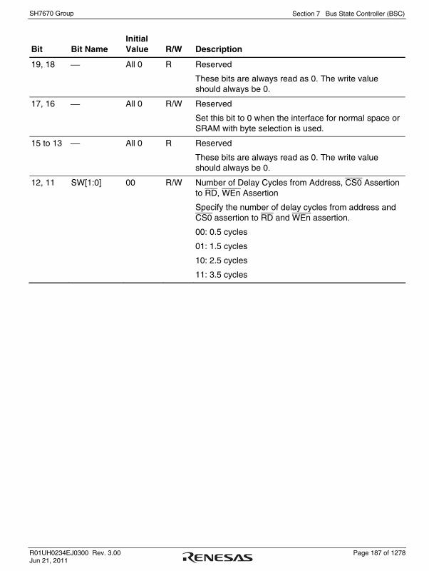
Section 7 Bus State Controller (BSC)
R01UH0234EJ0300 Rev. 3.00 Page 187 of 1278 Jun 21, 2011
SH7670 Group
Bit Bit Name Initial Value R/W Description
19, 18 ⎯ All 0 R Reserved
These bits are always read as 0. The write value should always be 0.
17, 16 ⎯ All 0 R/W Reserved
Set this bit to 0 when the interface for normal space or SRAM with byte selection is used.
15 to 13 ⎯ All 0 R Reserved
These bits are always read as 0. The write value should always be 0.
12, 11 SW[1:0] 00 R/W Number of Delay Cycles from Address, CS0 Assertion to RD, WEn Assertion
Specify the number of delay cycles from address and CS0 assertion to RD and WEn assertion.
00: 0.5 cycles
01: 1.5 cycles
10: 2.5 cycles
11: 3.5 cycles
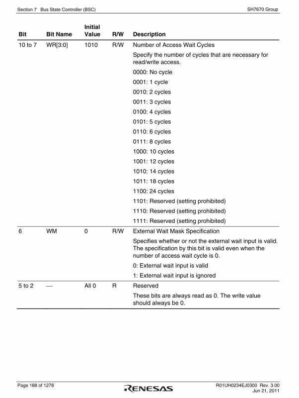
Section 7 Bus State Controller (BSC)
Page 188 of 1278 R01UH0234EJ0300 Rev. 3.00 Jun 21, 2011
SH7670 Group
Bit Bit Name Initial Value R/W Description
10 to 7 WR[3:0] 1010 R/W Number of Access Wait Cycles
Specify the number of cycles that are necessary for read/write access.
0000: No cycle
0001: 1 cycle
0010: 2 cycles
0011: 3 cycles
0100: 4 cycles
0101: 5 cycles
0110: 6 cycles
0111: 8 cycles
1000: 10 cycles
1001: 12 cycles
1010: 14 cycles
1011: 18 cycles
1100: 24 cycles
1101: Reserved (setting prohibited)
1110: Reserved (setting prohibited)
1111: Reserved (setting prohibited)
6 WM 0 R/W External Wait Mask Specification
Specifies whether or not the external wait input is valid. The specification by this bit is valid even when the number of access wait cycle is 0.
0: External wait input is valid
1: External wait input is ignored
5 to 2 ⎯ All 0 R Reserved
These bits are always read as 0. The write value should always be 0.

Section 7 Bus State Controller (BSC)
R01UH0234EJ0300 Rev. 3.00 Page 189 of 1278 Jun 21, 2011
SH7670 Group
Bit Bit Name Initial Value R/W Description
1, 0 HW[1:0] 00 R/W Delay Cycles from RD, WEn Negation to Address, CS0Negation
Specify the number of delay cycles from RD and WEn negation to address and CS0 negation.
00: 0.5 cycles
01: 1.5 cycles
10: 2.5 cycles
11: 3.5 cycles
• CS3WCR
31 30 29 28 27 26 25 24 23 22 21 20 19 18 17 16Bit:
Initial Value:R/W:
Bit:
Initial Value:R/W:
15 14 13 12 11 10 9 8 7 6 5 4 3 2 1 0
0 0 0 0 0 0 0 0 0 0 0 0 0 0 0 0R R R R R R R R R R R R/W R R R R
0 0 0 0 0 1 0 1 0 0 0 0 0 0 0 0R R R R R R/W R/W R/W R/W R/W R R R R R R
⎯ ⎯ ⎯ ⎯ ⎯ ⎯ ⎯ ⎯ ⎯ ⎯ ⎯ BAS ⎯ ⎯ ⎯ ⎯
⎯ ⎯ ⎯ ⎯ ⎯ WR[3:0] WM ⎯ ⎯ ⎯ ⎯ ⎯ ⎯
Bit Bit Name Initial Value R/W Description
31 to 21 ⎯ All 0 R Reserved
These bits are always read as 0. The write value should always be 0.
20 BAS 0 R/W SRAM with Byte Selection Byte Access Select
Specifies the WEn and RD/WR signal timing when the SRAM interface with byte selection is used.
0: Asserts the WEn signal at the read timing and asserts the RD/WR signal during the write access cycle.
1: Asserts the WEn signal during the read access cycle and asserts the RD/WR signal at the write timing.
19 to 11 ⎯ All 0 R Reserved
These bits are always read as 0. The write value should always be 0.

Section 7 Bus State Controller (BSC)
Page 190 of 1278 R01UH0234EJ0300 Rev. 3.00 Jun 21, 2011
SH7670 Group
Bit Bit Name Initial Value R/W Description
10 to 7 WR[3:0] 1010 R/W Number of Access Wait Cycles
Specify the number of cycles that are necessary for read/write access.
0000: No cycle
0001: 1 cycle
0010: 2 cycles
0011: 3 cycles
0100: 4 cycles
0101: 5 cycles
0110: 6 cycles
0111: 8 cycles
1000: 10 cycles
1001: 12 cycles
1010: 14 cycles
1011: 18 cycles
1100: 24 cycles
1101: Reserved (setting prohibited)
1110: Reserved (setting prohibited)
1111: Reserved (setting prohibited)
6 WM 0 R/W External Wait Mask Specification
Specifies whether or not the external wait input is valid. The specification by this bit is valid even when the number of access wait cycle is 0.
0: External wait input is valid
1: External wait input is ignored
5 to 0 ⎯ All 0 R Reserved
These bits are always read as 0. The write value should always be 0.

Section 7 Bus State Controller (BSC)
R01UH0234EJ0300 Rev. 3.00 Page 191 of 1278 Jun 21, 2011
SH7670 Group
• CS4WCR
31 30 29 28 27 26 25 24 23 22 21 20 19 18 17 16
15 14 13 12 11 10 9 8 7 6 5 4 3 2 1 0
0 0 0 0 0 0 0 0 0 0 0 0 0 0 0 0R R R R R R R R R R R R/W R R/W R/W R/W
0 0 0 0 0 1 0 1 0 0 0 0 0 0 0 0R R R R/W R/W R/W R/W R/W R/W R/W R R R R R/W R/W
Bit:
Initial value:R/W:
Bit:
Initial value:R/W:
- - - - - - - - - - - BAS - WW[2:0]
- - - SW[1:0] WR[3:0] WM - - - - HW[1:0]
Bit Bit Name Initial Value R/W Description
31 to 21 ⎯ All 0 R Reserved
These bits are always read as 0. The write value should always be 0.
20 BAS 0 R/W SRAM with Byte Selection Byte Access Select
Specifies the WEn and RD/WR signal timing when the SRAM interface with byte selection is used.
0: Asserts the WEn signal at the read timing and asserts the RD/WR signal during the write access cycle.
1: Asserts the WEn signal during the read access cycle and asserts the RD/WR signal at the write timing.
19 ⎯ 0 R Reserved
This bit is always read as 0. The write value should always be 0.
18 to 16 WW[2:0] 000 R/W Number of Write Access Wait Cycles
Specify the number of cycles that are necessary for write access.
000: The same cycles as WR[3:0] setting (number of read access wait cycles)
001: No cycle
010: 1 cycle
011: 2 cycles
100: 3 cycles
101: 4 cycles
110: 5 cycles
111: 6 cycles

Section 7 Bus State Controller (BSC)
Page 192 of 1278 R01UH0234EJ0300 Rev. 3.00 Jun 21, 2011
SH7670 Group
Bit Bit Name Initial Value R/W Description
15 to 13 ⎯ All 0 R Reserved
These bits are always read as 0. The write value should always be 0.
12, 11 SW[1:0] 00 R/W Number of Delay Cycles from Address, CS4 Assertion to RD, WE Assertion
Specify the number of delay cycles from address and CS4 assertion to RD and WE assertion.
00: 0.5 cycles
01: 1.5 cycles
10: 2.5 cycles
11: 3.5 cycles
10 to 7 WR[3:0] 1010 R/W Number of Read Access Wait Cycles
Specify the number of cycles that are necessary for read access.
0000: No cycle
0001: 1 cycle
0010: 2 cycles
0011: 3 cycles
0100: 4 cycles
0101: 5 cycles
0110: 6 cycles
0111: 8 cycles
1000: 10 cycles
1001: 12 cycles
1010: 14 cycles
1011: 18 cycles
1100: 24 cycles
1101: Reserved (setting prohibited)
1110: Reserved (setting prohibited)
1111: Reserved (setting prohibited)

Section 7 Bus State Controller (BSC)
R01UH0234EJ0300 Rev. 3.00 Page 193 of 1278 Jun 21, 2011
SH7670 Group
Bit Bit Name Initial Value R/W Description
6 WM 0 R/W External Wait Mask Specification
Specifies whether or not the external wait input is valid. The specification by this bit is valid even when the number of access wait cycle is 0.
0: External wait input is valid
1: External wait input is ignored
5 to 2 ⎯ All 0 R Reserved
These bits are always read as 0. The write value should always be 0.
1, 0 HW[1:0] 00 R/W Delay Cycles from RD, WEn Negation to Address, CS4Negation
Specify the number of delay cycles from RD and WEn negation to address and CS4 negation.
00: 0.5 cycles
01: 1.5 cycles
10: 2.5 cycles
11: 3.5 cycles

Section 7 Bus State Controller (BSC)
Page 194 of 1278 R01UH0234EJ0300 Rev. 3.00 Jun 21, 2011
SH7670 Group
• CS5WCR
31 30 29 28 27 26 25 24 23 22 21 20 19 18 17 16
15 14 13 12 11 10 9 8 7 6 5 4 3 2 1 0
0 0 0 0 0 0 0 0 0 0 0 0 0 0 0 0R R R R R R R R R R R R/W R R/W R/W R/W
0 0 0 0 0 1 0 1 0 0 0 0 0 0 0 0R R R R/W R/W R/W R/W R/W R/W R/W R R R R R/W R/W
Bit:
Initial value:R/W:
Bit:
Initial value:R/W:
- - - - - - - - - - -MPXW/
BAS - WW[2:0]
- - - SW[1:0] WR[3:0] WM - - - - HW[1:0]
Bit Bit Name Initial Value R/W Description
31 to 21 ⎯ All 0 R Reserved
These bits are always read as 0. The write value should always be 0.
20 BAS 0 R/W SRAM with Byte Selection Byte Access Select
Specifies the WEn and RD/WR signal timing when the SRAM interface with byte selection is used.
0: Asserts the WEn signal at the read timing and asserts the RD/WR signal during the write access cycle.
1: Asserts the WEn signal during the read access cycle and asserts the RD/WR signal at the write timing.
19 ⎯ 0 R Reserved
This bit is always read as 0. The write value should always be 0.
18 to 16 WW[2:0] 000 R/W Number of Write Access Wait Cycles
Specify the number of cycles that are necessary for write access.
000: The same cycles as WR[3:0] setting (number of read access wait cycles)
001: No cycle
010: 1 cycle
011: 2 cycles
100: 3 cycles
101: 4 cycles
110: 5 cycles
111: 6 cycles

Section 7 Bus State Controller (BSC)
R01UH0234EJ0300 Rev. 3.00 Page 195 of 1278 Jun 21, 2011
SH7670 Group
Bit Bit Name Initial Value R/W Description
15 to 13 ⎯ All 0 R Reserved
These bits are always read as 0. The write value should always be 0.
12, 11 SW[1:0] 00 R/W Number of Delay Cycles from Address, CS5 Assertion to RD, WEn Assertion
Specify the number of delay cycles from address and CS5 assertion to RD and WEn assertion.
00: 0.5 cycles
01: 1.5 cycles
10: 2.5 cycles
11: 3.5 cycles
10 to 7 WR[3:0] 1010 R/W Number of Read Access Wait Cycles
Specify the number of cycles that are necessary for read access.
0000: No cycle
0001: 1 cycle
0010: 2 cycles
0011: 3 cycles
0100: 4 cycles
0101: 5 cycles
0110: 6 cycles
0111: 8 cycles
1000: 10 cycles
1001: 12 cycles
1010: 14 cycles
1011: 18 cycles
1100: 24 cycles
1101: Reserved (setting prohibited)
1110: Reserved (setting prohibited)
1111: Reserved (setting prohibited)
6 WM 0 R/W External Wait Mask Specification
Specifies whether or not the external wait input is valid. The specification by this bit is valid even when the number of access wait cycle is 0.
0: External wait input is valid
1: External wait input is ignored

Section 7 Bus State Controller (BSC)
Page 196 of 1278 R01UH0234EJ0300 Rev. 3.00 Jun 21, 2011
SH7670 Group
Bit Bit Name Initial Value R/W Description
5 to 2 ⎯ All 0 R Reserved
These bits are always read as 0. The write value should always be 0.
1, 0 HW[1:0] 00 R/W Delay Cycles from RD, WEn Negation to Address, CS5 Negation
Specify the number of delay cycles from RD and WEn negation to address and CS5 negation.
00: 0.5 cycles
01: 1.5 cycles
10: 2.5 cycles
11: 3.5 cycles
• CS6WCR
31 30 29 28 27 26 25 24 23 22 21 20 19 18 17 16
15 14 13 12 11 10 9 8 7 6 5 4 3 2 1 0
0 0 0 0 0 0 0 0 0 0 0 0 0 0 0 0R R R R R R R R R R R R/W R R R R
0 0 0 0 0 1 0 1 0 0 0 0 0 0 0 0R R R R/W R/W R/W R/W R/W R/W R/W R R R R R/W R/W
Bit:
Initial value:R/W:
Bit:
Initial value:R/W:
- - - - - - - - - - - BAS - - - -
- - - SW[1:0] WR[3:0] WM - - - - HW[1:0]
Bit Bit Name Initial Value R/W Description
31 to 21 ⎯ All 0 R Reserved
These bits are always read as 0. The write value should always be 0.
20 BAS 0 R/W SRAM with Byte Selection Byte Access Select
Specifies the WEn and RD/WR signal timing when the SRAM interface with byte selection is used.
0: Asserts the WEn signal at the read timing and asserts the RD/WR signal during the write access cycle.
1: Asserts the WEn signal during the read/write access cycle and asserts the RD/WR signal at the write timing.

Section 7 Bus State Controller (BSC)
R01UH0234EJ0300 Rev. 3.00 Page 197 of 1278 Jun 21, 2011
SH7670 Group
Bit Bit Name Initial Value R/W Description
19 to 13 ⎯ All 0 R Reserved
These bits are always read as 0. The write value should always be 0.
12, 11 SW[1:0] 00 R/W Number of Delay Cycles from Address, CS6 Assertion to RD, WEn Assertion
Specify the number of delay cycles from address, CS6 assertion to RD and WEn assertion.
00: 0.5 cycles
01: 1.5 cycles
10: 2.5 cycles
11: 3.5 cycles
10 to 7 WR[3:0] 1010 R/W Number of Access Wait Cycles
Specify the number of cycles that are necessary for read/write access.
0000: No cycle
0001: 1 cycle
0010: 2 cycles
0011: 3 cycles
0100: 4 cycles
0101: 5 cycles
0110: 6 cycles
0111: 8 cycles
1000: 10 cycles
1001: 12 cycles
1010: 14 cycles
1011: 18 cycles
1100: 24 cycles
1101: Reserved (setting prohibited)
1110: Reserved (setting prohibited)
1111: Reserved (setting prohibited)
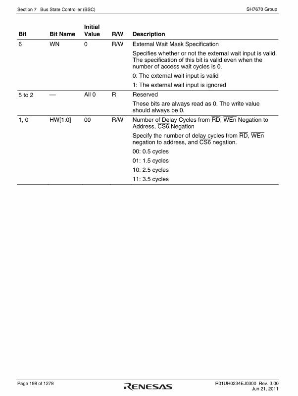
Section 7 Bus State Controller (BSC)
Page 198 of 1278 R01UH0234EJ0300 Rev. 3.00 Jun 21, 2011
SH7670 Group
Bit Bit Name Initial Value R/W Description
6 WN 0 R/W External Wait Mask Specification
Specifies whether or not the external wait input is valid. The specification of this bit is valid even when the number of access wait cycles is 0.
0: The external wait input is valid
1: The external wait input is ignored
5 to 2 ⎯ All 0 R Reserved
These bits are always read as 0. The write value should always be 0.
1, 0 HW[1:0] 00 R/W Number of Delay Cycles from RD, WEn Negation to Address, CS6 Negation
Specify the number of delay cycles from RD, WEn negation to address, and CS6 negation.
00: 0.5 cycles
01: 1.5 cycles
10: 2.5 cycles
11: 3.5 cycles

Section 7 Bus State Controller (BSC)
R01UH0234EJ0300 Rev. 3.00 Page 199 of 1278 Jun 21, 2011
SH7670 Group
(2) SDRAM
• CS3WCR
31 30 29 28 27 26 25 24 23 22 21 20 19 18 17 16
15 14 13 12 11 10 9 8 7 6 5 4 3 2 1 0
0 0 0 0 0 0 0 0 0 0 0 0 0 0 0 0R R R R R R R R R R R R R R R R
0 0 0 0 0 1 0 1 0 0 0 0 0 0 0 0R R/W R/W R R/W R/W R R/W R/W R R R/W R/W R R/W R/W
Bit:
Initial value:R/W:
Bit:
Initial value:R/W:
- - - - - - - - - - - - - - - -
- WTRP[1:0] WTRCD[1:0] TRWL[1:0] WTRC[1:0]- - A3CL[1:0] - - -
Bit Bit Name Initial Value R/W Description
31 to 15 ⎯ All 0 R Reserved
These bits are always read as 0. The write value should always be 0.
14, 13 WTRP[1:0] 00 R/W Number of Auto-Precharge Completion Wait Cycles
Specify the number of minimum precharge completion wait cycles as shown below.
• From the start of auto-precharge and issuing of
ACTV command for the same bank
• From issuing of the PRE/PALL command to issuing
of the ACTV command for the same bank
• Till entering the power-down mode or deep power-
down mode
• From the issuing of PALL command to issuing REF
command in auto refresh mode
• From the issuing of PALL command to issuing
SELF command in self refresh mode
00: No cycle
01: 1 cycle
10: 2 cycles
11: 3 cycles

Section 7 Bus State Controller (BSC)
Page 200 of 1278 R01UH0234EJ0300 Rev. 3.00 Jun 21, 2011
SH7670 Group
Bit Bit Name Initial Value R/W Description
12 ⎯ 0 R Reserved
This bit is always read as 0. The write value should always be 0.
11, 10 WTRCD[1:0] 01 R/W Number of Wait Cycles between ACTV Command and READ(A)/WRIT(A) Command
Specify the minimum number of wait cycles from issuing the ACTV command to issuing the READ(A)/WRIT(A) command.
00: No cycle
01: 1 cycle
10: 2 cycles
11: 3 cycles
9 ⎯ 0 R Reserved
This bit is always read as 0. The write value should always be 0.
8, 7 A3CL[1:0] 10 R/W CAS Latency for Area 3
Specify the CAS latency for area 3.
00: 1 cycle
01: 2 cycles
10: 3 cycles
11: 4 cycles
6, 5 ⎯ All 0 R Reserved
These bits are always read as 0. The write value should always be 0.
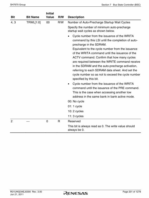
Section 7 Bus State Controller (BSC)
R01UH0234EJ0300 Rev. 3.00 Page 201 of 1278 Jun 21, 2011
SH7670 Group
Bit Bit Name Initial Value R/W Description
4, 3 TRWL[1:0] 00 R/W Number of Auto-Precharge Startup Wait Cycles
Specify the number of minimum auto-precharge startup wait cycles as shown below.
• Cycle number from the issuance of the WRITA command by this LSI until the completion of auto-
precharge in the SDRAM.
Equivalent to the cycle number from the issuance of the WRITA command until the issuance of the
ACTV command. Confirm that how many cycles
are required between the WRITE command receive in the SDRAM and the auto-precharge activation,
referring to each SDRAM data sheet. And set the
cycle number so as not to exceed the cycle number
specified by this bit.
• Cycle number from the issuance of the WRITA
command until the issuance of the PRE command.
This is the case when accessing another low
address in the same bank in bank active mode.
00: No cycle
01: 1 cycle
10: 2 cycles
11: 3 cycles
2 ⎯ 0 R Reserved
This bit is always read as 0. The write value should always be 0.
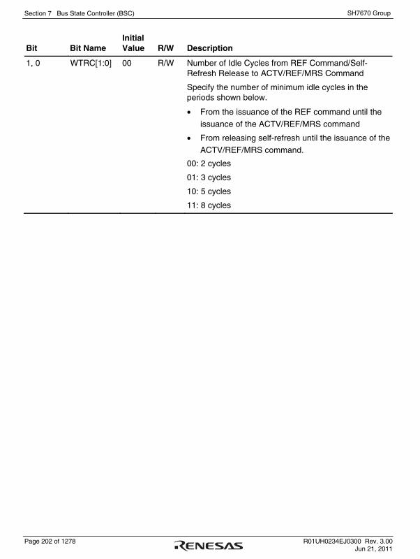
Section 7 Bus State Controller (BSC)
Page 202 of 1278 R01UH0234EJ0300 Rev. 3.00 Jun 21, 2011
SH7670 Group
Bit Bit Name Initial Value R/W Description
1, 0 WTRC[1:0] 00 R/W Number of Idle Cycles from REF Command/Self-Refresh Release to ACTV/REF/MRS Command
Specify the number of minimum idle cycles in the periods shown below.
• From the issuance of the REF command until the
issuance of the ACTV/REF/MRS command
• From releasing self-refresh until the issuance of the
ACTV/REF/MRS command.
00: 2 cycles
01: 3 cycles
10: 5 cycles
11: 8 cycles

Section 7 Bus State Controller (BSC)
R01UH0234EJ0300 Rev. 3.00 Page 203 of 1278 Jun 21, 2011
SH7670 Group
(3) PCMCIA
• CS5WCR, CS6WCR
31 30 29 28 27 26 25 24 23 22 21 20 19 18 17 16
15 14 13 12 11 10 9 8 7 6 5 4 3 2 1 0
0 0 0 0 0 0 0 0 0 0 0 0 0 0 0 0R R R R R R R R R R R/W R/W R R R R
0 0 0 0 0 1 0 1 0 0 0 0 0 0 0 0R R/W R/W R/W R/W R/W R/W R/W R/W R R R R/W R/W R/W R/W
Bit:
Initial value:R/W:
Bit:
Initial value:R/W:
- - - - - - - - - - SA[1:0] - - - -
- TED[3:0] PCW[3:0] TEH[3:0]WM - -
Bit Bit Name Initial Value R/W Description
31 to 22 ⎯ All 0 R Reserved
These bits are always read as 0. The write value should always be 0.
21, 20 SA[1:0] 00 R/W Space Attribute Specification
Select memory card interface or I/O card interface when PCMCIA interface is selected.
SA1:
0: Selects memory card interface for the space for A25 = 1.
1: Selects I/O card interface for the space for A25 = 1.
SA0:
0: Selects memory card interface for the space for A25 = 0.
1: Selects I/O card interface for the space for A25 = 0.
19 to 15 ⎯ All 0 R Reserved
These bits are always read as 0. The write value should always be 0.
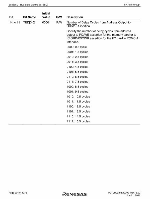
Section 7 Bus State Controller (BSC)
Page 204 of 1278 R01UH0234EJ0300 Rev. 3.00 Jun 21, 2011
SH7670 Group
Bit Bit Name Initial Value R/W Description
14 to 11 TED[3:0] 0000 R/W Number of Delay Cycles from Address Output to RD/WE Assertion
Specify the number of delay cycles from address output to RD/WE assertion for the memory card or to ICIORD/ICIOWR assertion for the I/O card in PCMCIA interface.
0000: 0.5 cycle
0001: 1.5 cycles
0010: 2.5 cycles
0011: 3.5 cycles
0100: 4.5 cycles
0101: 5.5 cycles
0110: 6.5 cycles
0111: 7.5 cycles
1000: 8.5 cycles
1001: 9.5 cycles
1010: 10.5 cycles
1011: 11.5 cycles
1100: 12.5 cycles
1101: 13.5 cycles
1110: 14.5 cycles
1111: 15.5 cycles

Section 7 Bus State Controller (BSC)
R01UH0234EJ0300 Rev. 3.00 Page 205 of 1278 Jun 21, 2011
SH7670 Group
Bit Bit Name Initial Value R/W Description
10 to 7 PCW[3:0] 1010 R/W Number of Access Wait Cycles
Specify the number of wait cycles to be inserted.
0000: 3 cycles
0001: 6 cycles
0010: 9 cycles
0011: 12 cycles
0100: 15 cycles
0101: 18 cycles
0110: 22 cycles
0111: 26 cycles
1000: 30 cycles
1001: 33 cycles
1010: 36 cycles
1011: 38 cycles
1100: 52 cycles
1101: 60 cycles
1110: 64 cycles
1111: 80 cycles
6 WM 0 R/W External Wait Mask Specification
Specifies whether or not the external wait input is valid. The specification by this bit is valid even when the number of access wait cycles is 0.
0: External wait input is valid
1: External wait input is ignored
5, 4 ⎯ All 0 R Reserved
These bits are always read as 0. The write value should always be 0.
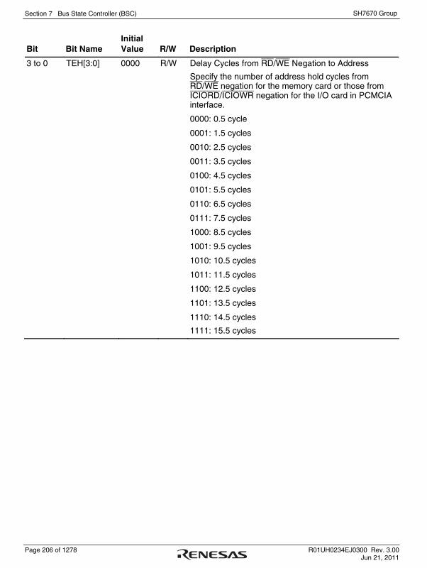
Section 7 Bus State Controller (BSC)
Page 206 of 1278 R01UH0234EJ0300 Rev. 3.00 Jun 21, 2011
SH7670 Group
Bit Bit Name Initial Value R/W Description
3 to 0 TEH[3:0] 0000 R/W Delay Cycles from RD/WE Negation to Address
Specify the number of address hold cycles from RD/WE negation for the memory card or those from ICIORD/ICIOWR negation for the I/O card in PCMCIA interface.
0000: 0.5 cycle
0001: 1.5 cycles
0010: 2.5 cycles
0011: 3.5 cycles
0100: 4.5 cycles
0101: 5.5 cycles
0110: 6.5 cycles
0111: 7.5 cycles
1000: 8.5 cycles
1001: 9.5 cycles
1010: 10.5 cycles
1011: 11.5 cycles
1100: 12.5 cycles
1101: 13.5 cycles
1110: 14.5 cycles
1111: 15.5 cycles

Section 7 Bus State Controller (BSC)
R01UH0234EJ0300 Rev. 3.00 Page 207 of 1278 Jun 21, 2011
SH7670 Group
7.4.4 SDRAM Control Register (SDCR)
SDCR specifies the method to refresh and access SDRAM, and the types of SDRAMs to be connected.
31 30 29 28 27 26 25 24 23 22 21 20 19 18 17 16Bit:
Initial Value:R/W:
15 14 13 12 11 10 9 8 7 6 5 4 3 2 1 0Bit:
Initial Value:R/W:
0 0 0 0 0 0 0 0 0 0 0 0 0 0 0 0R R R R R R R R R R R R R R R R
0 0 0 0 0 0 0 0 0 0 0 0 0 0 0 0R R R/W R R/W R/W R/W R/W R R R R/W R/W R R/W R/W
⎯ ⎯ ⎯ ⎯ ⎯ ⎯ ⎯ ⎯ ⎯ ⎯ ⎯ ⎯ ⎯
A3ROW[1:0] A3COL[1:0]
⎯ ⎯ ⎯
⎯ ⎯ DEEP ⎯ RFSH RMODEPDOWN BACTV ⎯ ⎯ ⎯ ⎯
Bit Bit Name Initial Value R/W Description
31 to 14 ⎯ All 0 R Reserved
These bits are always read as 0. The write value should always be 0.
13 DEEP 0 R/W Deep Power-Down Mode
This bit is valid for low-power SDRAM. If the RFSH or RMODE bit is set to 1 while this bit is set to 1, the deep power-down entry command is issued and the low-power SDRAM enters the deep power-down mode.
0: Self-refresh mode
1: Deep power-down mode
12 ⎯ 0 R Reserved
This bit is always read as 0. The write value should always be 0.
11 RFSH 0 R/W Refresh Control
Specifies whether or not the refresh operation of the SDRAM is performed.
0: No refresh
1: Refresh

Section 7 Bus State Controller (BSC)
Page 208 of 1278 R01UH0234EJ0300 Rev. 3.00 Jun 21, 2011
SH7670 Group
Bit Bit Name Initial Value R/W Description
10 RMODE 0 R/W Refresh Control
Specifies whether to perform auto-refresh or self-refresh when the RFSH bit is 1. When the RFSH bit is 1 and this bit is 1, self-refresh starts immediately. When the RFSH bit is 1 and this bit is 0, auto-refresh starts according to the contents that are set in registers RTCSR, RTCNT, and RTCOR.
0: Auto-refresh is performed
1: Self-refresh is performed
9 PDOWN 0 R/W Power-Down Mode
Specifies whether the SDRAM will enter the power-down mode after the access to the SDRAM. With this bit being set to 1, after the SDRAM is accessed, the CKE signal is driven low and the SDRAM enters the power-down mode.
0: The SDRAM does not enter the power-down mode after being accessed.
1: The SDRAM enters the power-down mode after being accessed.
8 BACTV 0 R/W Bank Active Mode
Specifies to access whether in auto-precharge mode (using READA and WRITA commands) or in bank active mode (using READ and WRIT commands).
0: Auto-precharge mode (using READA and WRITA commands)
1: Bank active mode (using READ and WRIT commands)
7 to 5 ⎯ All 0 R Reserved
These bits are always read as 0. The write value should always be 0.

Section 7 Bus State Controller (BSC)
R01UH0234EJ0300 Rev. 3.00 Page 209 of 1278 Jun 21, 2011
SH7670 Group
Bit Bit Name Initial Value R/W Description
4, 3 A3ROW[1:0] 00 R/W Number of Bits of Row Address for Area 3
Specify the number of bits of the row address for area 3.
00: 11 bits
01: 12 bits
10: 13 bits
11: Reserved (setting prohibited)
2 ⎯ 0 R Reserved
This bit is always read as 0. The write value should always be 0.
1, 0 A3COL[1:0] 00 R/W Number of Bits of Column Address for Area 3
Specify the number of bits of the column address for area 3.
00: 8 bits
01: 9 bits
10: 10 bits
11: Reserved (setting prohibited)
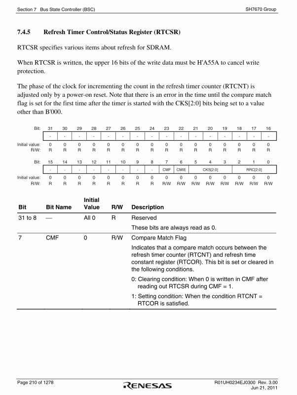
Section 7 Bus State Controller (BSC)
Page 210 of 1278 R01UH0234EJ0300 Rev. 3.00 Jun 21, 2011
SH7670 Group
7.4.5 Refresh Timer Control/Status Register (RTCSR)
RTCSR specifies various items about refresh for SDRAM.
When RTCSR is written, the upper 16 bits of the write data must be H'A55A to cancel write protection.
The phase of the clock for incrementing the count in the refresh timer counter (RTCNT) is adjusted only by a power-on reset. Note that there is an error in the time until the compare match flag is set for the first time after the timer is started with the CKS[2:0] bits being set to a value other than B'000.
31 30 29 28 27 26 25 24 23 22 21 20 19 18 17 16
15 14 13 12 11 10 9 8 7 6 5 4 3 2 1 0
0 0 0 0 0 0 0 0 0 0 0 0 0 0 0 0R R R R R R R R R R R R R R R R
0 0 0 0 0 0 0 0 0 0 0 0 0 0 0 0R R R R R R R R R/W R/W R/W R/W R/W R/W R/W R/W
Bit:
Initial value:R/W:
Bit:
Initial value:R/W:
- - - - - - - - - - - - - - - -
- - - - - - - - CMF CMIE CKS[2:0] RRC[2:0]
Bit Bit Name Initial Value R/W Description
31 to 8 ⎯ All 0 R Reserved
These bits are always read as 0.
7 CMF 0 R/W Compare Match Flag
Indicates that a compare match occurs between the refresh timer counter (RTCNT) and refresh time constant register (RTCOR). This bit is set or cleared in the following conditions.
0: Clearing condition: When 0 is written in CMF after reading out RTCSR during CMF = 1.
1: Setting condition: When the condition RTCNT = RTCOR is satisfied.
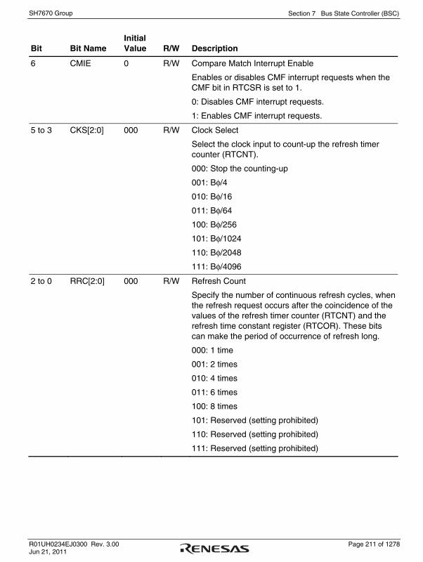
Section 7 Bus State Controller (BSC)
R01UH0234EJ0300 Rev. 3.00 Page 211 of 1278 Jun 21, 2011
SH7670 Group
Bit Bit Name Initial Value R/W Description
6 CMIE 0 R/W Compare Match Interrupt Enable
Enables or disables CMF interrupt requests when the CMF bit in RTCSR is set to 1.
0: Disables CMF interrupt requests.
1: Enables CMF interrupt requests.
5 to 3 CKS[2:0] 000 R/W Clock Select
Select the clock input to count-up the refresh timer counter (RTCNT).
000: Stop the counting-up
001: Bφ/4
010: Bφ/16
011: Bφ/64
100: Bφ/256
101: Bφ/1024
110: Bφ/2048
111: Bφ/4096
2 to 0 RRC[2:0] 000 R/W Refresh Count
Specify the number of continuous refresh cycles, when the refresh request occurs after the coincidence of the values of the refresh timer counter (RTCNT) and the refresh time constant register (RTCOR). These bits can make the period of occurrence of refresh long.
000: 1 time
001: 2 times
010: 4 times
011: 6 times
100: 8 times
101: Reserved (setting prohibited)
110: Reserved (setting prohibited)
111: Reserved (setting prohibited)

Section 7 Bus State Controller (BSC)
Page 212 of 1278 R01UH0234EJ0300 Rev. 3.00 Jun 21, 2011
SH7670 Group
7.4.6 Refresh Timer Counter (RTCNT)
RTCNT is an 8-bit counter that increments using the clock selected by bits CKS[2:0] in RTCSR. When RTCNT matches RTCOR, RTCNT is cleared to 0. The value in RTCNT returns to 0 after counting up to 255. When the RTCNT is written, the upper 16 bits of the write data must be H'A55A to cancel write protection.
31 30 29 28 27 26 25 24 23 22 21 20 19 18 17 16
15 14 13 12 11 10 9 8 7 6 5 4 3 2 1 0
0 0 0 0 0 0 0 0 0 0 0 0 0 0 0 0R R R R R R R R R R R R R R R R
0 0 0 0 0 0 0 0 0 0 0 0 0 0 0 0R R R R R R R R R/W R/W R/W R/W R/W R/W R/W R/W
Bit:
Initial value:R/W:
Bit:
Initial value:R/W:
- - - - - - - - - - - - - - - -
- - - - - - - -
Bit Bit Name Initial Value R/W Description
31 to 8 ⎯ All 0 R Reserved
These bits are always read as 0.
7 to 0 All 0 R/W 8-Bit Counter
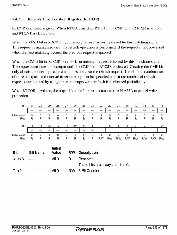
Section 7 Bus State Controller (BSC)
R01UH0234EJ0300 Rev. 3.00 Page 213 of 1278 Jun 21, 2011
SH7670 Group
7.4.7 Refresh Time Constant Register (RTCOR)
RTCOR is an 8-bit register. When RTCOR matches RTCNT, the CMF bit in RTCSR is set to 1 and RTCNT is cleared to 0.
When the RFSH bit in SDCR is 1, a memory refresh request is issued by this matching signal. This request is maintained until the refresh operation is performed. If the request is not processed when the next matching occurs, the previous request is ignored.
When the CMIE bit in RTCSR is set to 1, an interrupt request is issued by this matching signal. The request continues to be output until the CMF bit in RTCSR is cleared. Clearing the CMF bit only affects the interrupt request and does not clear the refresh request. Therefore, a combination of refresh request and interval timer interrupt can be specified so that the number of refresh requests are counted by using timer interrupts while refresh is performed periodically.
When RTCOR is written, the upper 16 bits of the write data must be H'A55A to cancel write protection.
31 30 29 28 27 26 25 24 23 22 21 20 19 18 17 16
15 14 13 12 11 10 9 8 7 6 5 4 3 2 1 0
0 0 0 0 0 0 0 0 0 0 0 0 0 0 0 0R R R R R R R R R R R R R R R R
0 0 0 0 0 0 0 0 0 0 0 0 0 0 0 0R R R R R R R R R/W R/W R/W R/W R/W R/W R/W R/W
Bit:
Initial value:R/W:
Bit:
Initial value:R/W:
⎯ ⎯ ⎯ ⎯ ⎯ ⎯ ⎯ ⎯ ⎯ ⎯ ⎯ ⎯ ⎯ ⎯ ⎯ ⎯
⎯ ⎯ ⎯ ⎯ ⎯ ⎯ ⎯ ⎯
Bit Bit Name Initial Value R/W Description
31 to 8 ⎯ All 0 R Reserved
These bits are always read as 0.
7 to 0 All 0 R/W 8-Bit Counter
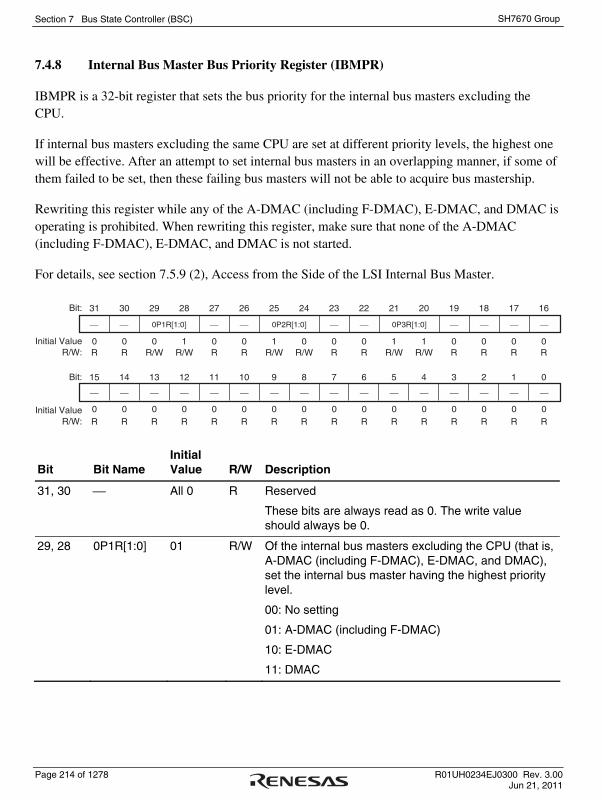
Section 7 Bus State Controller (BSC)
Page 214 of 1278 R01UH0234EJ0300 Rev. 3.00 Jun 21, 2011
SH7670 Group
7.4.8 Internal Bus Master Bus Priority Register (IBMPR)
IBMPR is a 32-bit register that sets the bus priority for the internal bus masters excluding the CPU.
If internal bus masters excluding the same CPU are set at different priority levels, the highest one will be effective. After an attempt to set internal bus masters in an overlapping manner, if some of them failed to be set, then these failing bus masters will not be able to acquire bus mastership.
Rewriting this register while any of the A-DMAC (including F-DMAC), E-DMAC, and DMAC is operating is prohibited. When rewriting this register, make sure that none of the A-DMAC (including F-DMAC), E-DMAC, and DMAC is not started.
For details, see section 7.5.9 (2), Access from the Side of the LSI Internal Bus Master.
31 30 29 28 27 26 25 24 23 22 21 20 19 18 17 16Bit:
Initial ValueR/W:
Bit:
Initial ValueR/W:
15 14 13 12 11 10 9 8 7 6 5 4 3 2 1 0
0 0 0 1 0 0 1 0 0 0 1 1 0 0 0 0R R R/W R/W R R R/W R/W R R R/W R/W R R R R
0 0 0 0 0 0 0 0R R R R R R R R
0 0 0 0 0 0 0 0R R R R R R R R
⎯ ⎯ 0P1R[1:0] ⎯ ⎯ 0P2R[1:0] ⎯ ⎯ 0P3R[1:0] ⎯ ⎯ ⎯ ⎯
⎯ ⎯ ⎯ ⎯ ⎯ ⎯ ⎯ ⎯ ⎯ ⎯ ⎯ ⎯ ⎯ ⎯ ⎯ ⎯
Bit Bit Name Initial Value R/W Description
31, 30 ⎯ All 0 R Reserved
These bits are always read as 0. The write value should always be 0.
29, 28 0P1R[1:0] 01 R/W Of the internal bus masters excluding the CPU (that is, A-DMAC (including F-DMAC), E-DMAC, and DMAC), set the internal bus master having the highest priority level.
00: No setting
01: A-DMAC (including F-DMAC)
10: E-DMAC
11: DMAC
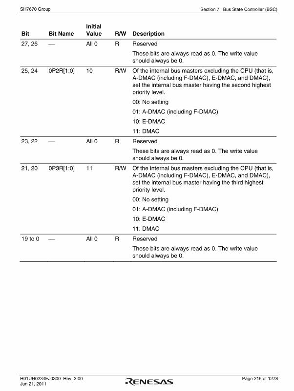
Section 7 Bus State Controller (BSC)
R01UH0234EJ0300 Rev. 3.00 Page 215 of 1278 Jun 21, 2011
SH7670 Group
Bit Bit Name Initial Value R/W Description
27, 26 ⎯ All 0 R Reserved
These bits are always read as 0. The write value should always be 0.
25, 24 0P2R[1:0] 10 R/W Of the internal bus masters excluding the CPU (that is, A-DMAC (including F-DMAC), E-DMAC, and DMAC), set the internal bus master having the second highest priority level.
00: No setting
01: A-DMAC (including F-DMAC)
10: E-DMAC
11: DMAC
23, 22 ⎯ All 0 R Reserved
These bits are always read as 0. The write value should always be 0.
21, 20 0P3R[1:0] 11 R/W Of the internal bus masters excluding the CPU (that is, A-DMAC (including F-DMAC), E-DMAC, and DMAC), set the internal bus master having the third highest priority level.
00: No setting
01: A-DMAC (including F-DMAC)
10: E-DMAC
11: DMAC
19 to 0 ⎯ All 0 R Reserved
These bits are always read as 0. The write value should always be 0.

Section 7 Bus State Controller (BSC)
Page 216 of 1278 R01UH0234EJ0300 Rev. 3.00 Jun 21, 2011
SH7670 Group
7.5 Operation
7.5.1 Endian/Access Size and Data Alignment
This LSI supports both big endian, in which the most significant byte (MSB) of data is that in the direction of the 0th address, and little endian, in which the least significant byte (LSB) is that in the direction of the 0th address. In the initial state after a power-on reset, all areas will be in big endian mode. Little endian cannot be selected for area 0. However, the endian of areas 3 to 6 can be changed by the setting in the CSnBCR register setting as long as the target space is not being accessed.
Three data bus widths (8 bits, 16 bits, and 32 bits) are selectable for areas 3 to 6, allowing the connection of normal memory and of SRAM with byte selection. Two data bus widths (16 bits and 32 bits) are available for SDRAM. Two data bus widths (8 bits and 16 bits) are available for the PCMCIA interface. For MPX-I/O, the data bus width can be fixed to either 8 or 16 bits, or made selectable as 8 bits or 16 bits by one of the address lines. Data alignment is in accord with the data bus width selected for the device. This also means that four read operations are required to read longword data from a byte-width device. In this LSI, data alignment and conversion of data length is performed automatically between the respective interfaces. The data bus width of area 0 is fixed to 8 bits or 16 bits by the MD_BW pin setting at a power-on reset.
Tables 7.5 to 7.10 show the relationship between device data width and access unit. Note that the correspondence between addresses and strobe signals for the 32- and 16-bit bus widths depends on the endian setting. For example, with big endian and a 32-bit bus width, WE3 corresponds to the 0th address, which is represented by WE0 when little endian has been selected. Little endian cannot be selected for area 0. Note also that 32-bit and 16-bit accesses coincide in instruction fetching, therefore, it is difficult to allocate instruction to little endian area. Make sure to execute instruction in big endian area.
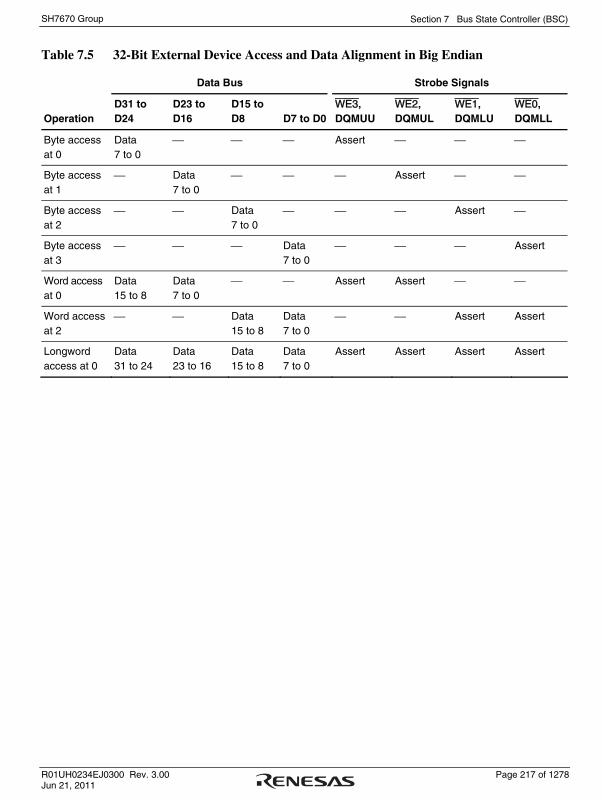
Section 7 Bus State Controller (BSC)
R01UH0234EJ0300 Rev. 3.00 Page 217 of 1278 Jun 21, 2011
SH7670 Group
Table 7.5 32-Bit External Device Access and Data Alignment in Big Endian
Data Bus Strobe Signals
Operation D31 to D24
D23 to D16
D15 to D8 D7 to D0
WE3, DQMUU
WE2, DQMUL
WE1, DQMLU
WE0, DQMLL
Byte access at 0
Data 7 to 0
⎯ ⎯ ⎯ Assert ⎯ ⎯ ⎯
Byte access at 1
⎯ Data 7 to 0
⎯ ⎯ ⎯ Assert ⎯ ⎯
Byte access at 2
⎯ ⎯ Data 7 to 0
⎯ ⎯ ⎯ Assert ⎯
Byte access at 3
⎯ ⎯ ⎯ Data 7 to 0
⎯ ⎯ ⎯ Assert
Word access at 0
Data 15 to 8
Data 7 to 0
⎯ ⎯ Assert Assert ⎯ ⎯
Word access at 2
⎯ ⎯ Data 15 to 8
Data 7 to 0
⎯ ⎯ Assert Assert
Longword access at 0
Data 31 to 24
Data 23 to 16
Data 15 to 8
Data 7 to 0
Assert Assert Assert Assert
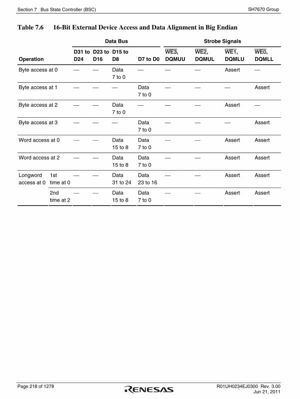
Section 7 Bus State Controller (BSC)
Page 218 of 1278 R01UH0234EJ0300 Rev. 3.00 Jun 21, 2011
SH7670 Group
Table 7.6 16-Bit External Device Access and Data Alignment in Big Endian
Data Bus Strobe Signals
Operation D31 to D24
D23 to D16
D15 to D8 D7 to D0
WE3, DQMUU
WE2, DQMUL
WE1, DQMLU
WE0, DQMLL
Byte access at 0 ⎯ ⎯ Data 7 to 0
⎯ ⎯ ⎯ Assert ⎯
Byte access at 1 ⎯ ⎯ ⎯ Data 7 to 0
⎯ ⎯ ⎯ Assert
Byte access at 2 ⎯ ⎯ Data 7 to 0
⎯ ⎯ ⎯ Assert ⎯
Byte access at 3 ⎯ ⎯ ⎯ Data 7 to 0
⎯ ⎯ ⎯ Assert
Word access at 0 ⎯ ⎯ Data 15 to 8
Data 7 to 0
⎯ ⎯ Assert Assert
Word access at 2 ⎯ ⎯ Data 15 to 8
Data 7 to 0
⎯ ⎯ Assert Assert
1st time at 0
⎯ ⎯ Data 31 to 24
Data 23 to 16
⎯ ⎯ Assert Assert Longword access at 0
2nd time at 2
⎯ ⎯ Data 15 to 8
Data 7 to 0
⎯ ⎯ Assert Assert

Section 7 Bus State Controller (BSC)
R01UH0234EJ0300 Rev. 3.00 Page 219 of 1278 Jun 21, 2011
SH7670 Group
Table 7.7 8-Bit External Device Access and Data Alignment in Big Endian
Data Bus Strobe Signals
Operation D31 to D24
D23 to D16
D15 to D8
D7 to D0
WE3, DQMUU
WE2, DQMUL
WE1, DQMLU
WE0, DQMLL
Byte access at 0 ⎯ ⎯ ⎯ Data 7 to 0
⎯ ⎯ ⎯ Assert
Byte access at 1 ⎯ ⎯ ⎯ Data 7 to 0
⎯ ⎯ ⎯ Assert
Byte access at 2 ⎯ ⎯ ⎯ Data 7 to 0
⎯ ⎯ ⎯ Assert
Byte access at 3 ⎯ ⎯ ⎯ Data 7 to 0
⎯ ⎯ ⎯ Assert
1st time at 0
⎯ ⎯ ⎯ Data 15 to 8
⎯ ⎯ ⎯ Assert Word access at 0
2nd time at 1
⎯ ⎯ ⎯ Data 7 to 0
⎯ ⎯ ⎯ Assert
1st time at 2
⎯ ⎯ ⎯ Data 15 to 8
⎯ ⎯ ⎯ Assert Word access at 2
2nd time at 3
⎯ ⎯ ⎯ Data 7 to 0
⎯ ⎯ ⎯ Assert
1st time at 0
⎯ ⎯ ⎯ Data 31 to 24
⎯ ⎯ ⎯ Assert
2nd time at 1
⎯ ⎯ ⎯ Data 23 to 16
⎯ ⎯ ⎯ Assert
3rd time at 2
⎯ ⎯ ⎯ Data 15 to 8
⎯ ⎯ ⎯ Assert
Longword access at 0
4th time at 3
⎯ ⎯ ⎯ Data 7 to 0
⎯ ⎯ ⎯ Assert

Section 7 Bus State Controller (BSC)
Page 220 of 1278 R01UH0234EJ0300 Rev. 3.00 Jun 21, 2011
SH7670 Group
Table 7.8 32-Bit External Device Access and Data Alignment in Little Endian
Data Bus Strobe Signals
Operation D31 to D24
D23 to D16
D15 to D8 D7 to D0
WE3, DQMUU
WE2, DQMUL
WE1, DQMLU
WE0, DQMLL
Byte access at 0
⎯ ⎯ ⎯ Data 7 to 0
⎯ ⎯ ⎯ Assert
Byte access at 1
⎯ ⎯ Data 7 to 0
⎯ ⎯ ⎯ Assert ⎯
Byte access at 2
⎯ Data 7 to 0
⎯ ⎯ ⎯ Assert ⎯ ⎯
Byte access at 3
Data 7 to 0
⎯ ⎯ ⎯ Assert ⎯ ⎯ ⎯
Word access at 0
⎯ ⎯ Data 15 to 8
Data 7 to 0
⎯ ⎯ Assert Assert
Word access at 2
Data 15 to 8
Data 7 to 0
⎯ ⎯ Assert Assert ⎯ ⎯
Longword access at 0
Data 31 to 24
Data 23 to 16
Data 15 to 8
Data 7 to 0
Assert Assert Assert Assert

Section 7 Bus State Controller (BSC)
R01UH0234EJ0300 Rev. 3.00 Page 221 of 1278 Jun 21, 2011
SH7670 Group
Table 7.9 16-Bit External Device Access and Data Alignment in Little Endian
Data Bus Strobe Signals
Operation D31 to D24
D23 to D16
D15 to D8 D7 to D0
WE3, DQMUU
WE2, DQMUL
WE1, DQMLU
WE0, DQMLL
Byte access at 0 ⎯ ⎯ ⎯ Data 7 to 0
⎯ ⎯ ⎯ Assert
Byte access at 1 ⎯ ⎯ Data 7 to 0
⎯ ⎯ ⎯ Assert ⎯
Byte access at 2 ⎯ ⎯ ⎯ Data 7 to 0
⎯ ⎯ ⎯ Assert
Byte access at 3 ⎯ ⎯ Data 7 to 0
⎯ ⎯ ⎯ Assert ⎯
Word access at 0 ⎯ ⎯ Data 15 to 8
Data 7 to 0
⎯ ⎯ Assert Assert
Word access at 2 ⎯ ⎯ Data 15 to 8
Data 7 to 0
⎯ ⎯ Assert Assert
1st time at 0
⎯ ⎯ Data 15 to 8
Data 7 to 0
⎯ ⎯ Assert Assert Longword access at 0
2nd time at 2
⎯ ⎯ Data 31 to 24
Data 23 to 16
⎯ ⎯ Assert Assert

Section 7 Bus State Controller (BSC)
Page 222 of 1278 R01UH0234EJ0300 Rev. 3.00 Jun 21, 2011
SH7670 Group
Table 7.10 8-Bit External Device Access and Data Alignment in Little Endian
Data Bus Strobe Signals
Operation D31 to D24
D23 to D16
D15 to D8
D7 to D0
WE3, DQMUU
WE2, DQMUL
WE1, DQMLU
WE0, DQMLL
Byte access at 0 ⎯ ⎯ ⎯ Data 7 to 0
⎯ ⎯ ⎯ Assert
Byte access at 1 ⎯ ⎯ ⎯ Data 7 to 0
⎯ ⎯ ⎯ Assert
Byte access at 2 ⎯ ⎯ ⎯ Data 7 to 0
⎯ ⎯ ⎯ Assert
Byte access at 3 ⎯ ⎯ ⎯ Data 7 to 0
⎯ ⎯ ⎯ Assert
1st time at 0
⎯ ⎯ ⎯ Data 7 to 0
⎯ ⎯ ⎯ Assert Word access at 0
2nd time at 1
⎯ ⎯ ⎯ Data 15 to 8
⎯ ⎯ ⎯ Assert
1st time at 2
⎯ ⎯ ⎯ Data 7 to 0
⎯ ⎯ ⎯ Assert Word access at 2
2nd time at 3
⎯ ⎯ ⎯ Data 15 to 8
⎯ ⎯ ⎯ Assert
1st time at 0
⎯ ⎯ ⎯ Data 7 to 0
⎯ ⎯ ⎯ Assert
2nd time at 1
⎯ ⎯ ⎯ Data 15 to 8
⎯ ⎯ ⎯ Assert
3rd time at 2
⎯ ⎯ ⎯ Data 23 to 16
⎯ ⎯ ⎯ Assert
Longword access at 0
4th time at 3
⎯ ⎯ ⎯ Data 31 to 24
⎯ ⎯ ⎯ Assert

Section 7 Bus State Controller (BSC)
R01UH0234EJ0300 Rev. 3.00 Page 223 of 1278 Jun 21, 2011
SH7670 Group
7.5.2 Normal Space Interface
(1) Basic Timing
For access to a normal space, this LSI uses strobe signal output in consideration of the fact that mainly static RAM will be directly connected. When using SRAM with a byte-selection pin, see section 7.5.6, SRAM Interface with Byte Selection. Figure 7.2 shows the basic timings of normal space access. A no-wait normal access is completed in two cycles. The BS signal is asserted for one cycle to indicate the start of a bus cycle.
CKIO
Note: * The waveform for DACKn is when active low is specified.
A25 to A0
RD/WR
RD/WR
D31 to D0
DACKn
CSn
T1 T2
RD
WEn
BS
D31 to D0
Read
Write
*
Figure 7.2 Normal Space Basic Access Timing (Access Wait 0)
There is no access size specification when reading. The correct access start address is output in the least significant bit of the address, but since there is no access size specification, 32 bits are always

Section 7 Bus State Controller (BSC)
Page 224 of 1278 R01UH0234EJ0300 Rev. 3.00 Jun 21, 2011
SH7670 Group
read in case of a 32-bit device, and 16 bits in case of a 16-bit device. When writing, only the WEn signal for the byte to be written is asserted.
It is necessary to output the data that has been read using RD when a buffer is established in the data bus. The RD/WR signal is in a read state (high output) when no access has been carried out. Therefore, care must be taken when controlling the external data buffer, to avoid collision.
Figures 7.3 and 7.4 show the basic timings of normal space access. If the WM bit in CSnWCR is cleared to 0, a Tnop cycle is inserted after the CSn space access to evaluate the external wait (figure 7.3). If the WM bit in CSnWCR is set to 1, external waits are ignored and no Tnop cycle is inserted (figure 7.4).
CKIO
A25 to A0
RD
RD/WR
D15 to D0
WEn
D15 to D0
DACKn
BS
WAIT
CSn
T1 T2 Tnop T1 T2
Read
Write
*
Note: * The waveform for DACKn is when active low is specified.
Figure 7.3 Continuous Access for Normal Space 1 Bus Width = 16 Bits, Longword Access, CSnWCR.WM Bit = 0
(Access Wait = 0, Cycle Wait = 0)

Section 7 Bus State Controller (BSC)
R01UH0234EJ0300 Rev. 3.00 Page 225 of 1278 Jun 21, 2011
SH7670 Group
CKIO
A25 to A0
RD/WR
D15 to D0
DACKn
CSn
T1 T2 T1 T2
RD
WEn
BS
WAIT
D15 to D0
Read
Write
*
Note: * The waveform for DACKn is when active low is specified.
Figure 7.4 Continuous Access for Normal Space 2 Bus Width = 16 Bits, Longword Access, CSnWCR.WM Bit = 1
(Access Wait = 0, Cycle Wait = 0)
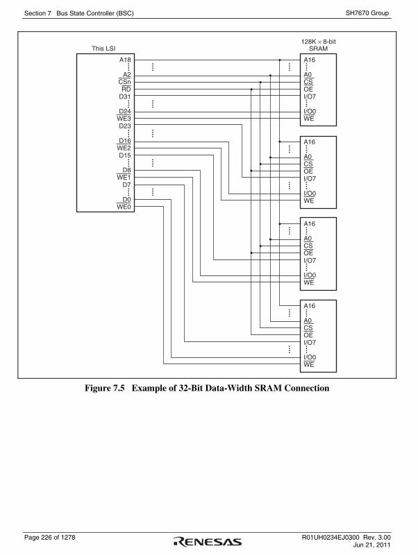
Section 7 Bus State Controller (BSC)
Page 226 of 1278 R01UH0234EJ0300 Rev. 3.00 Jun 21, 2011
SH7670 Group
••••
••••
••••
••••
••••
A16
A0CSOEI/O7
I/O0WE
••••
••••
••••
••••
A18
A2CSnRD
D31
D24WE3D23
D16WE2D15
D8WE1
D7
D0WE0
This LSI128K × 8-bit
SRAM
••••
A16
A0CSOEI/O7
I/O0WE
••••
••••
••••
••••
••••
A16
A0CSOEI/O7
I/O0WE
••••
••••
••••
••••
A16
A0CSOEI/O7
I/O0WE
••••
••••
••••
••••
••••
Figure 7.5 Example of 32-Bit Data-Width SRAM Connection

Section 7 Bus State Controller (BSC)
R01UH0234EJ0300 Rev. 3.00 Page 227 of 1278 Jun 21, 2011
SH7670 Group
A16
A0CSOEI/O7
I/O0WE
••••
••••
••••
••••
A17
A1CSnRD
D15
D8WE1
D7
D0WE0
This LSI128K × 8-bit
SRAM
••••
A16
A0CSOEI/O7
I/O0WE
••••
••••
••••
••••
••••
••••
••••
••••
Figure 7.6 Example of 16-Bit Data-Width SRAM Connection
This LSI128K × 8-bit
SRAM
A16
A0
CS
OE
I/O7
I/O0
WE
. . .
A16
A0
CSn
RD
D7
D0
WE0
. . .
. . .
. . .
Figure 7.7 Example of 8-Bit Data-Width SRAM Connection

Section 7 Bus State Controller (BSC)
Page 228 of 1278 R01UH0234EJ0300 Rev. 3.00 Jun 21, 2011
SH7670 Group
7.5.3 Access Wait Control
Wait cycle insertion on a normal space access can be controlled by the settings of bits WR3 to WR0 in CSnWCR. It is possible for areas 4 and 5 to insert wait cycles independently in read access and in write access. Areas 0, 3, and 6 have common access wait for read cycle and write cycle. The specified number of Tw cycles are inserted as wait cycles in a normal space access shown in figure 7.8.
T1
CKIO
A25 to A0
CSn
RD/WR
RD
D31 to D0
WEn
D31 to D0
BS
Tw
Read
Write
T2
DACKn*
Note: * The waveform for DACKn is when active low is specified.
Figure 7.8 Wait Timing for Normal Space Access (Software Wait Only)

Section 7 Bus State Controller (BSC)
R01UH0234EJ0300 Rev. 3.00 Page 229 of 1278 Jun 21, 2011
SH7670 Group
When the WM bit in CSnWCR is cleared to 0, the external wait input WAIT signal is also sampled. WAIT pin sampling is shown in figure 7.9. A 2-cycle wait is specified as a software wait. The WAIT signal is sampled on the falling edge of CKIO at the transition from the T1 or Tw cycle to the T2 cycle.
T1
CKIO
A25 to A0
CSn
RD/WR
RD
D31 to D0
WEn
D31 to D0
WAIT
Tw Tw Twx T2
Read
Write
BS
Wait states insertedby WAIT signal
DACKn*
Note: * The waveform for DACKn is when active low is specified.
Figure 7.9 Wait Cycle Timing for Normal Space Access (Wait Cycle Insertion Using WAIT Signal)

Section 7 Bus State Controller (BSC)
Page 230 of 1278 R01UH0234EJ0300 Rev. 3.00 Jun 21, 2011
SH7670 Group
7.5.4 CSn Assert Period Expansion
The number of cycles from CSn assertion to RD, WEn assertion can be specified by setting bits SW1 and SW0 in CSnWCR. The number of cycles from RD, WEn negation to CSn negation can be specified by setting bits HW1 and HW0. Therefore, a flexible interface to an external device can be obtained. Figure 7.10 shows an example. A Th cycle and a Tf cycle are added before and after an ordinary cycle, respectively. In these cycles, RD and WEn are not asserted, while other signals are asserted. The data output is prolonged to the Tf cycle, and this prolongation is useful for devices with slow writing operations.
T1
CKIO
A25 to A0
CSn
RD/WR
RD
D31 to D0
WEn
D31 to D0
BS
Th
Read
Write
T2
DACKn*
Tf
Note: * The waveform for DACKn is when active low is specified.
Figure 7.10 CSn Assert Period Expansion

Section 7 Bus State Controller (BSC)
R01UH0234EJ0300 Rev. 3.00 Page 231 of 1278 Jun 21, 2011
SH7670 Group
7.5.5 SDRAM Interface
(1) SDRAM Direct Connection
The SDRAM that can be connected to this LSI is a product that has 11/12/13 bits of row address, 8/9/10 bits of column address, 4 or less banks, and uses the A10 pin for setting precharge mode in read and write command cycles.
The control signals for direct connection of SDRAM are RAS, CAS, RD/WR, DQMUU, DQMUL, DQMLU, DQMLL, CKE, and CS3. All the signals other than CS3 are common to all areas, and signals other than CKE are valid when CS2 or CS3 is asserted. SDRAM can be connected to up to 2 spaces. The data bus width of the area that is connected to SDRAM can be set to 32 or 16 bits.
Burst read/single write (burst length 1) and burst read/burst write (burst length 1) are supported as the SDRAM operating mode.
Commands for SDRAM can be specified by RAS, CAS, RD/WR, and specific address signals. These commands supports:
• NOP
• Auto-refresh (REF)
• Self-refresh (SELF)
• All banks pre-charge (PALL)
• Specified bank pre-charge (PRE)
• Bank active (ACTV)
• Read (READ)
• Read with pre-charge (READA)
• Write (WRIT)
• Write with pre-charge (WRITA)
• Write mode register (MRS, EMRS) The byte to be accessed is specified by DQMUU, DQMUL, DQMLU, and DQMLL. Reading or writing is performed for a byte whose corresponding DQMxx is low. For details on the relationship between DQMxx and the byte to be accessed, see section 7.5.1, Endian/Access Size and Data Alignment.
Figures 7.11 and 7.12 show examples of the connection of the SDRAM with the LSI.

Section 7 Bus State Controller (BSC)
Page 232 of 1278 R01UH0234EJ0300 Rev. 3.00 Jun 21, 2011
SH7670 Group
A15
A2CKE
CKIOCSn
RAS
CAS
RD/WR
D31
D16DQMUUDQMUL
D15
D0DQMLUDQMLL
64M SDRAM(1M×16Bits×4Bank)
A13
A0CKECLKCS
RAS
CAS
WE
I/O15
I/O0DQMUDQML
A13
A0CKECLKCS
RAS
CAS
WE
I/O15
I/O0DQMUDQML
This LSI
••••
••••
••••
••••
••••
••••
••••
Figure 7.11 Example of 32-Bit Data Width SDRAM Connection

Section 7 Bus State Controller (BSC)
R01UH0234EJ0300 Rev. 3.00 Page 233 of 1278 Jun 21, 2011
SH7670 Group
A14
A1CKE
CKIOCSn
RAS
CAS
RD/WR
D15
D0DQMLUDQMLL
A13
A0CKECLKCS
RAS
CAS
WE
I/O15
I/O0DQMUDQML
This LSI
••••
••••••••
••••
64M SDRAM(1M×16Bits×4Bank)
Figure 7.12 Example of 16-Bit Data Width SDRAM Connection

Section 7 Bus State Controller (BSC)
Page 234 of 1278 R01UH0234EJ0300 Rev. 3.00 Jun 21, 2011
SH7670 Group
(2) Address Multiplexing
An address multiplexing is specified so that SDRAM can be connected without external multiplexing circuitry according to the setting of bits BSZ[1:0] in CSnBCR, bits A2ROW[1:0], and A2COL[1:0], A3ROW[1:0], and A3COL[1:0] in SDCR. Tables 7.11 to 7.16 show the relationship between the settings of bits BSZ[1:0], A2ROW[1:0], A2COL[1:0], A3ROW[1:0], and A3COL[1:0] and the bits output at the address pins. Do not specify those bits in the manner other than this table, otherwise the operation of this LSI is not guaranteed. A25 to A18 are not multiplexed and the original values of address are always output at these pins.
When the data bus width is 16 bits (BSZ1 and BSZ0 = B'10), A0 of SDRAM specifies a word address. Therefore, connect this A0 pin of SDRAM to the A1 pin of the LSI; the A1 pin of SDRAM to the A2 pin of the LSI, and so on. When the data bus width is 32 bits (BSZ1 and BSZ0 = B'11), the A0 pin of SDRAM specifies a longword address. Therefore, connect this A0 pin of SDRAM to the A2 pin of the LSI; the A1 pin of SDRAM to the A3 pin of the LSI, and so on.
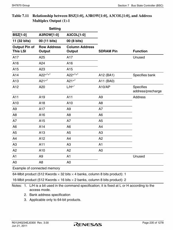
Section 7 Bus State Controller (BSC)
R01UH0234EJ0300 Rev. 3.00 Page 235 of 1278 Jun 21, 2011
SH7670 Group
Table 7.11 Relationship between BSZ[1:0], A3ROW[1:0], A3COL[1:0], and Address Multiplex Output (1)-1
Setting
BSZ[1:0] A3ROW[1:0] A3COL[1:0]
11 (32 bits) 00 (11 bits) 00 (8 bits)
Output Pin of This LSI
Row Address Output
Column Address Output
SDRAM Pin
Function
A17 A25 A17
A16 A24 A16
A15 A23 A15
Unused
A14 A22*2*3 A22*2*3 A12 (BA1)
A13 A21*2 A21*2 A11 (BA0)
Specifies bank
A12 A20 L/H*1 A10/AP Specifies address/precharge
A11 A19 A11 A9
A10 A18 A10 A8
A9 A17 A9 A7
A8 A16 A8 A6
A7 A15 A7 A5
A6 A14 A6 A4
A5 A13 A5 A3
A4 A12 A4 A2
A3 A11 A3 A1
A2 A10 A2 A0
Address
A1 A9 A1
A0 A8 A0
Unused
Example of connected memory
64-Mbit product (512 Kwords × 32 bits × 4 banks, column 8 bits product): 1
16-Mbit product (512 Kwords × 16 bits × 2 banks, column 8 bits product): 2
Notes: 1. L/H is a bit used in the command specification; it is fixed at L or H according to the access mode.
2. Bank address specification
3. Applicable only to 64-bit products.

Section 7 Bus State Controller (BSC)
Page 236 of 1278 R01UH0234EJ0300 Rev. 3.00 Jun 21, 2011
SH7670 Group
Table 7.11 Relationship between BSZ[1:0], A3ROW[1:0], A3COL[1:0], and Address Multiplex Output (1)-2
Setting
BSZ[1:0] A3ROW[1:0] A3COL[1:0]
11 (32 bits) 01 (12 bits) 00 (8 bits)
Output Pin of This LSI
Row Address Output
Column Address Output
SDRAM Pin
Function
A17 A25 A17
A16 A24 A16
Unused
A15 A23*2 A23*2 A13 (BA1)
A14 A22*2 A22*2 A12 (BA0)
Specifies bank
A13 A21 A13 A11 Address
A12 A20 L/H*1 A10/AP Specifies address/precharge
A11 A19 A11 A9
A10 A18 A10 A8
A9 A17 A9 A7
A8 A16 A8 A6
A7 A15 A7 A5
A6 A14 A6 A4
A5 A13 A5 A3
A4 A12 A4 A2
A3 A11 A3 A1
A2 A10 A2 A0
Address
A1 A9 A1
A0 A8 A0
Unused
Example of connected memory
128-Mbit product (1 Mword × 32 bits × 4 banks, column 8 bits product): 1
64-Mbit product (1 Mword × 16 bits × 4 banks, column 8 bits product): 2
Notes: 1. L/H is a bit used in the command specification; it is fixed at L or H according to the access mode.
2. Bank address specification
3. Applicable only to 64-bit products.

Section 7 Bus State Controller (BSC)
R01UH0234EJ0300 Rev. 3.00 Page 237 of 1278 Jun 21, 2011
SH7670 Group
Table 7.12 Relationship between BSZ[1:0], A3ROW[1:0], A3COL[1:0], and Address Multiplex Output (2)-1
Setting
BSZ[1:0] A3ROW[1:0] A3COL[1:0]
11 (32 bits) 01 (12 bits) 01 (9 bits)
Output Pin of This LSI
Row Address Output
Column Address Output
SDRAM Pin
Function
A17 A26 A17
A16 A25 A16
Unused
A15 A24*2 A24*2 A13 (BA1)
A14 A23*2 A23*2 A12 (BA0)
Specifies bank
A13 A22 A13 A11 Address
A12 A21 L/H*1 A10/AP Specifies address/precharge
A11 A20 A11 A9
A10 A19 A10 A8
A9 A18 A9 A7
A8 A17 A8 A6
A7 A16 A7 A5
A6 A15 A6 A4
A5 A14 A5 A3
A4 A13 A4 A2
A3 A12 A3 A1
A2 A11 A2 A0
Address
A1 A10 A1
A0 A9 A0
Unused
Example of connected memory
256-Mbit product (2 Mwords × 32 bits × 4 banks, column 9 bits product): 1
128-Mbit product (2 Mwords × 16 bits × 4 banks, column 9 bits product): 2
Notes: 1. L/H is a bit used in the command specification; it is fixed at L or H according to the access mode.
2. Bank address specification
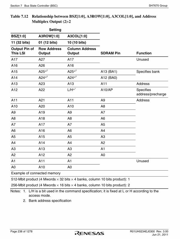
Section 7 Bus State Controller (BSC)
Page 238 of 1278 R01UH0234EJ0300 Rev. 3.00 Jun 21, 2011
SH7670 Group
Table 7.12 Relationship between BSZ[1:0], A3ROW[1:0], A3COL[1:0], and Address Multiplex Output (2)-2
Setting
BSZ[1:0] A3ROW[1:0] A3COL[1:0]
11 (32 bits) 01 (12 bits) 10 (10 bits)
Output Pin of This LSI
Row Address Output
Column Address Output SDRAM Pin Function
A17 A27 A17
A16 A26 A16
Unused
A15 A25*2 A25*2 A13 (BA1)
A14 A24*2 A24*2 A12 (BA0)
Specifies bank
A13 A23 A13 A11 Address
A12 A22 L/H*1 A10/AP Specifies address/precharge
A11 A21 A11 A9
A10 A20 A10 A8
A9 A19 A9 A7
A8 A18 A8 A6
A7 A17 A7 A5
A6 A16 A6 A4
A5 A15 A5 A3
A4 A14 A4 A2
A3 A13 A3 A1
A2 A12 A2 A0
Address
A1 A11 A1
A0 A10 A0
Unused
Example of connected memory
512-Mbit product (4 Mwords × 32 bits × 4 banks, column 10 bits product): 1
256-Mbit product (4 Mwords × 16 bits × 4 banks, column 10 bits product): 2
Notes: 1. L/H is a bit used in the command specification; it is fixed at L or H according to the access mode.
2. Bank address specification

Section 7 Bus State Controller (BSC)
R01UH0234EJ0300 Rev. 3.00 Page 239 of 1278 Jun 21, 2011
SH7670 Group
Table 7.13 Relationship between BSZ[1:0], A3ROW[1:0], A3COL[1:0], and Address Multiplex Output (3)
Setting
BSZ[1:0] A3ROW[1:0] A3COL[1:0]
11 (32 bits) 10 (13 bits) 01 (9 bits)
Output Pin of This LSI
Row Address Output
Column Address Output SDRAM Pin Function
A17 A26 A17 Unused
A16 A25*2 A25*2 A14 (BA1)
A15 A24*2 A24*2 A13 (BA0)
Specifies bank
A14 A23 A14 A12
A13 A22 A13 A11
Address
A12 A21 L/H*1 A10/AP Specifies address/precharge
A11 A20 A11 A9
A10 A19 A10 A8
A9 A18 A9 A7
A8 A17 A8 A6
A7 A16 A7 A5
A6 A15 A6 A4
A5 A14 A5 A3
A4 A13 A4 A2
A3 A12 A3 A1
A2 A11 A2 A0
Address
A1 A10 A1
A0 A9 A0
Unused
Example of connected memory
512-Mbit product (4 Mwords × 32 bits × 4 banks, column 9 bits product): 1
256-Mbit product (4 Mwords × 16 bits × 4 banks, column 9 bits product): 2
Notes: 1. L/H is a bit used in the command specification; it is fixed at L or H according to the access mode.
2. Bank address specification
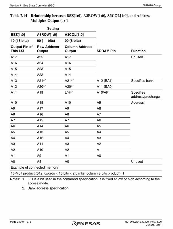
Section 7 Bus State Controller (BSC)
Page 240 of 1278 R01UH0234EJ0300 Rev. 3.00 Jun 21, 2011
SH7670 Group
Table 7.14 Relationship between BSZ[1:0], A3ROW[1:0], A3COL[1:0], and Address Multiplex Output (4)-1
Setting
BSZ[1:0] A3ROW[1:0] A3COL[1:0]
10 (16 bits) 00 (11 bits) 00 (8 bits)
Output Pin of This LSI
Row Address Output
Column Address Output SDRAM Pin Function
A17 A25 A17
A16 A24 A16
A15 A23 A15
A14 A22 A14
Unused
A13 A21*2 A21*2 A12 (BA1)
A12 A20*2 A20*2 A11 (BA0)
Specifies bank
A11 A19 L/H*1 A10/AP Specifies address/precharge
A10 A18 A10 A9
A9 A17 A9 A8
A8 A16 A8 A7
A7 A15 A7 A6
A6 A14 A6 A5
A5 A13 A5 A4
A4 A12 A4 A3
A3 A11 A3 A2
A2 A10 A2 A1
A1 A9 A1 A0
Address
A0 A8 A0 Unused
Example of connected memory
16-Mbit product (512 Kwords × 16 bits × 2 banks, column 8 bits product): 1
Notes: 1. L/H is a bit used in the command specification; it is fixed at low or high according to the access mode.
2. Bank address specification

Section 7 Bus State Controller (BSC)
R01UH0234EJ0300 Rev. 3.00 Page 241 of 1278 Jun 21, 2011
SH7670 Group
Table 7.14 Relationship between BSZ[1:0], A3ROW[1:0], A3COL[1:0], and Address Multiplex Output (4)-2
Setting
BSZ[1:0] A3ROW[1:0] A3COL[1:0]
10 (16 bits) 01 (12 bits) 00 (8 bits)
Output Pin of This LSI
Row Address Output
Column Address Output SDRAM Pin Function
A17 A25 A17
A16 A24 A16
A15 A23 A15
Unused
A14 A22*2 A22*2 A13 (BA1)
A13 A21*2 A21*2 A12 (BA0)
Specifies bank
A12 A20 A12 A11 Address
A11 A19 L/H*1 A10/AP Specifies address/precharge
A10 A18 A10 A9
A9 A17 A9 A8
A8 A16 A8 A7
A7 A15 A7 A6
A6 A14 A6 A5
A5 A13 A5 A4
A4 A12 A4 A3
A3 A11 A3 A2
A2 A10 A2 A1
A1 A9 A1 A0
Address
A0 A8 A0 Unused
Example of connected memory
64-Mbit product (1 Mword × 16 bits × 4 banks, column 8 bits product): 1
Notes: 1. L/H is a bit used in the command specification; it is fixed at L or H according to the access mode.
2. Bank address specification

Section 7 Bus State Controller (BSC)
Page 242 of 1278 R01UH0234EJ0300 Rev. 3.00 Jun 21, 2011
SH7670 Group
Table 7.15 Relationship between BSZ[1:0], A3ROW[1:0], A3COL[1:0], and Address Multiplex Output (5)-1
Setting
BSZ[1:0] A3ROW[1:0] A3COL[1:0]
10 (16 bits) 01 (12 bits) 01 (9 bits)
Output Pin of This LSI
Row Address Output
Column Address Output SDRAM Pin Function
A17 A26 A17
A16 A25 A16
A15 A24 A15
Unused
A14 A23*2 A23*2 A13 (BA1)
A13 A22*2 A22*2 A12 (BA0)
Specifies bank
A12 A21 A12 A11 Address
A11 A20 L/H*1 A10/AP Specifies address/precharge
A10 A19 A10 A9
A9 A18 A9 A8
A8 A17 A8 A7
A7 A16 A7 A6
A6 A15 A6 A5
A5 A14 A5 A4
A4 A13 A4 A3
A3 A12 A3 A2
A2 A11 A2 A1
A1 A10 A1 A0
Address
A0 A9 A0 Unused
Example of connected memory
128-Mbit product (2 Mwords × 16 bits × 4 banks, column 9 bits product): 1
Notes: 1. L/H is a bit used in the command specification; it is fixed at low or high according to the access mode.
2. Bank address specification

Section 7 Bus State Controller (BSC)
R01UH0234EJ0300 Rev. 3.00 Page 243 of 1278 Jun 21, 2011
SH7670 Group
Table 7.15 Relationship between BSZ[1:0], A3ROW[1:0], A3COL[1:0], and Address Multiplex Output (5)-2
Setting
BSZ[1:0] A3ROW[1:0] A3COL[1:0]
10 (16 bits) 01 (12 bits) 10 (10 bits)
Output Pin of This LSI
Row Address Output
Column Address Output SDRAM Pin Function
A17 A27 A17
A16 A26 A16
A15 A25 A15
Unused
A14 A24*2 A24*2 A13 (BA1)
A13 A23*2 A23*2 A12 (BA0)
Specifies bank
A12 A22 A12 A11 Address
A11 A21 L/H*1 A10/AP Specifies address/precharge
A10 A20 A10 A9
A9 A19 A9 A8
A8 A18 A8 A7
A7 A17 A7 A6
A6 A16 A6 A5
A5 A15 A5 A4
A4 A14 A4 A3
A3 A13 A3 A2
A2 A12 A2 A1
A1 A11 A1 A0
Address
A0 A10 A0 Unused
Example of connected memory
256-Mbit product (4 Mwords × 16 bits × 4 banks, column 10 bits product): 1
Notes: 1. L/H is a bit used in the command specification; it is fixed at low or high according to the access mode.
2. Bank address specification

Section 7 Bus State Controller (BSC)
Page 244 of 1278 R01UH0234EJ0300 Rev. 3.00 Jun 21, 2011
SH7670 Group
Table 7.16 Relationship between BSZ[1:0], A3ROW[1:0], A3COL[1:0], and Address Multiplex Output (6)-1
Setting
BSZ[1:0] A3ROW[1:0] A3COL[1:0]
10 (16 bits) 10 (13 bits) 01 (9 bits)
Output Pin of This LSI
Row Address Output
Column Address Output SDRAM Pin Function
A17 A26 A17
A16 A25 A16
Unused
A15 A24*2 A24*2 A14 (BA1)
A14 A23*2 A23*2 A13 (BA0)
Specifies bank
A13 A22 A13 A12
A12 A21 A12 A11
Address
A11 A20 L/H*1 A10/AP Specifies address/precharge
A10 A19 A10 A9
A9 A18 A9 A8
A8 A17 A8 A7
A7 A16 A7 A6
A6 A15 A6 A5
A5 A14 A5 A4
A4 A13 A4 A3
A3 A12 A3 A2
A2 A11 A2 A1
A1 A10 A1 A0
Address
A0 A9 A0 Unused
Example of connected memory
256-Mbit product (4 Mwords × 16 bits × 4 banks, column 9 bits product): 1
Notes: 1. L/H is a bit used in the command specification; it is fixed at low or high according to the access mode.
2. Bank address specification

Section 7 Bus State Controller (BSC)
R01UH0234EJ0300 Rev. 3.00 Page 245 of 1278 Jun 21, 2011
SH7670 Group
Table 7.16 Relationship between BSZ[1:0], A3ROW[1:0], A3COL[1:0], and Address Multiplex Output (6)-2
Setting
BSZ[1:0] A3ROW[1:0] A3COL[1:0]
10 (16 bits) 10 (13 bits) 10 (10 bits)
Output Pin of This LSI
Row Address Output
Column Address Output SDRAM Pin Function
A17 A27 A17
A16 A26 A16
Unused
A15 A25*2 A25*2 A14 (BA1)
A14 A24*2 A24*2 A13 (BA0)
Specifies bank
A13 A23 A13 A12
A12 A22 A12 A11
Address
A11 A21 L/H*1 A10/AP Specifies address/precharge
A10 A20 A10 A9
A9 A19 A9 A8
A8 A18 A8 A7
A7 A17 A7 A6
A6 A16 A6 A5
A5 A15 A5 A4
A4 A14 A4 A3
A3 A13 A3 A2
A2 A12 A2 A1
A1 A11 A1 A0
Address
A0 A10 A0 Unused
Example of connected memory
512-Mbit product (8 Mwords × 16 bits × 4 banks, column 10 bits product): 1
Notes: 1. L/H is a bit used in the command specification; it is fixed at low or high according to the access mode.
2. Bank address specification

Section 7 Bus State Controller (BSC)
Page 246 of 1278 R01UH0234EJ0300 Rev. 3.00 Jun 21, 2011
SH7670 Group
(3) Burst Read
A burst read occurs in the following cases with this LSI.
• Access size in reading is larger than data bus width.
• 16-byte transfer in cache miss.
• 16-byte transfer by DMAC This LSI always accesses the SDRAM with burst length 1. For example, read access of burst length 1 is performed consecutively 4 times to read 16-byte continuous data from the SDRAM that is connected to a 32-bit data bus. This access is called the burst read with the burst number 4. Table 7.17 shows the relationship between the access size and the number of bursts.
Table 7.17 Relationship between Access Size and Number of Bursts
Bus Width Access Size Number of Bursts
16 bits 8 bits 1
16 bits 1
32 bits 2
16 bits 8
32 bits 8 bits 1
16 bits 1
32 bits 1
16 bytes* 4

Section 7 Bus State Controller (BSC)
R01UH0234EJ0300 Rev. 3.00 Page 247 of 1278 Jun 21, 2011
SH7670 Group
Figures 7.13 and 7.14 show a timing chart in burst read. In burst read, an ACTV command is output in the Tr cycle, the READ command is issued in the Tc1, Tc2, and Tc3 cycles, the READA command is issued in the Tc4 cycle, and the read data is received at the rising edge of the external clock (CKIO) in the Td1 to Td4 cycles. The Tap cycle is used to wait for the completion of an auto-precharge induced by the READA command in the SDRAM. In the Tap cycle, a new command will not be issued to the same bank. However, access to another CS space or another bank in the same SDRAM space is enabled. The number of Tap cycles is specified by the WTRP1 and WTRP0 bits in CS3WCR.
In this LSI, wait cycles can be inserted by specifying each bit in CS3WCR to connect the SDRAM in variable frequencies. Figure 7.14 shows an example in which wait cycles are inserted. The number of cycles from the Tr cycle where the ACTV command is output to the Tc1 cycle where the READ command is output can be specified using the WTRCD1 and WTRCD0 bits in CS3WCR. If the WTRCD1 and WTRCD0 bits specify one cycles or more, a Trw cycle where the NOT command is issued is inserted between the Tr cycle and Tc1 cycle. The number of cycles from the Tc1 cycle where the READ command is output to the Td1 cycle where the read data is latched can be specified for the CS2 and CS3 spaces independently, using the A2CL1 and A2CL0 bits in CS2WCR or the A3CL1 and A3CL0 bits in CS3WCR and WTRCD0 bit in CS3WCR. The number of cycles from Tc1 to Td1 corresponds to the SDRAM CAS latency. The CAS latency for the SDRAM is normally defined as up to three cycles. However, the CAS latency in this LSI can be specified as 1 to 4 cycles. This CAS latency can be achieved by connecting a latch circuit between this LSI and the SDRAM.
A Tde cycle is an idle cycle required to transfer the read data into this LSI and occurs once for every burst read or every single read.

Section 7 Bus State Controller (BSC)
Page 248 of 1278 R01UH0234EJ0300 Rev. 3.00 Jun 21, 2011
SH7670 Group
Tc4
CKIO
A25 to A0
CSn
RD/WR
RASL, RASU
DQMxx
D31 to D0
BS
(Tap)
DACKn*2
Tr Tc2 Tc3Tc1Td4
TdeTd2 Td3Td1
A12/A11*1
CASL, CASU
Notes: 1. Address pin to be connected to pin A10 of SDRAM. 2. The waveform for DACKn is when active low is specified.
Figure 7.13 Burst Read Basic Timing (CAS Latency 1, Auto Pre-Charge)
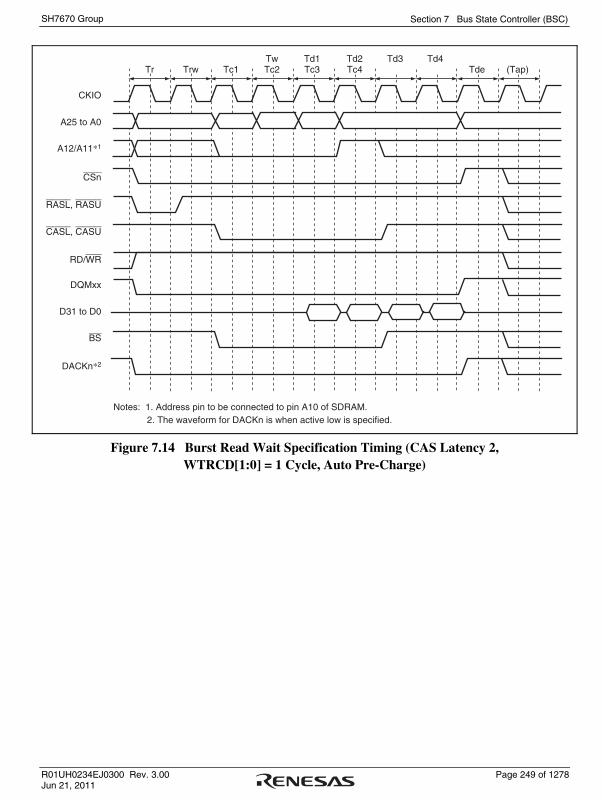
Section 7 Bus State Controller (BSC)
R01UH0234EJ0300 Rev. 3.00 Page 249 of 1278 Jun 21, 2011
SH7670 Group
Tc4 (Tap)Tr Tc2 Tc3Tc1Td4
TdeTd2 Td3Td1
TrwTw
CKIO
A25 to A0
CSn
RD/WR
RASL, RASU
DQMxx
D31 to D0
BS
DACKn*2
A12/A11*1
CASL, CASU
Notes: 1. Address pin to be connected to pin A10 of SDRAM. 2. The waveform for DACKn is when active low is specified.
Figure 7.14 Burst Read Wait Specification Timing (CAS Latency 2, WTRCD[1:0] = 1 Cycle, Auto Pre-Charge)
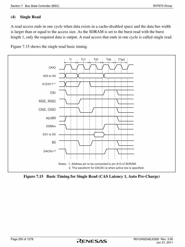
Section 7 Bus State Controller (BSC)
Page 250 of 1278 R01UH0234EJ0300 Rev. 3.00 Jun 21, 2011
SH7670 Group
(4) Single Read
A read access ends in one cycle when data exists in a cache-disabled space and the data bus width is larger than or equal to the access size. As the SDRAM is set to the burst read with the burst length 1, only the required data is output. A read access that ends in one cycle is called single read.
Figure 7.15 shows the single read basic timing.
(Tap)Tr Tc1 TdeTd1
CKIO
A25 to A0
CSn
RD/WR
RASL, RASU
DQMxx
D31 to D0
BS
DACKn*2
A12/A11*1
CASL, CASU
Notes: 1. Address pin to be connected to pin A10 of SDRAM. 2. The waveform for DACKn is when active low is specified.
Figure 7.15 Basic Timing for Single Read (CAS Latency 1, Auto Pre-Charge)

Section 7 Bus State Controller (BSC)
R01UH0234EJ0300 Rev. 3.00 Page 251 of 1278 Jun 21, 2011
SH7670 Group
(5) Burst Write
A burst write occurs in the following cases in this LSI.
• Access size in writing is larger than data bus width.
• Write-back of the cache
• 16-byte transfer in DMAC This LSI always accesses SDRAM with burst length 1. For example, write access of burst length 1 is performed continuously 4 times to write 16-byte continuous data to the SDRAM that is connected to a 32-bit data bus. This access is called burst write with the burst number 4. The relationship between the access size and the number of bursts is shown in table 7.17. Figure 7.16 shows a timing chart for burst writes. In burst write, an ACTV command is output in the Tr cycle, the WRIT command is issued in the Tc1, Tc2, and Tc3 cycles, and the WRITA command is issued to execute an auto-precharge in the Tc4 cycle. In the write cycle, the write data is output simultaneously with the write command. After the write command with the auto-precharge is output, the Trw1 cycle that waits for the auto-precharge initiation is followed by the Tap cycle that waits for completion of the auto-precharge induced by the WRITA command in the SDRAM. Between the Trwl and the Tap cycle, a new command will not be issued to the same bank. However, access to another CS space or another bank in the same SDRAM space is enabled. The number of Trw1 cycles is specified by the TRWL1 and TRWL0 bits in CS3WCR. The number of Tap cycles is specified by the WTRP1 and WTRP0 bits in CS3WCR.

Section 7 Bus State Controller (BSC)
Page 252 of 1278 R01UH0234EJ0300 Rev. 3.00 Jun 21, 2011
SH7670 Group
Tc4 TapTr Tc2 Tc3Tc1 Trwl
CKIO
A25 to A0
CSn
RD/WR
RASL, RASU
DQMxx
D31 to D0
BS
DACKn*2
A12/A11*1
CASL, CASU
Notes: 1. Address pin to be connected to pin A10 of SDRAM. 2. The waveform for DACKn is when active low is specified.
Figure 7.16 Basic Timing for Burst Write (Auto Pre-Charge)
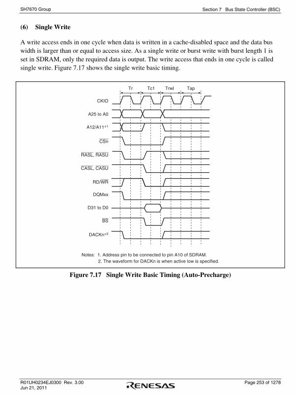
Section 7 Bus State Controller (BSC)
R01UH0234EJ0300 Rev. 3.00 Page 253 of 1278 Jun 21, 2011
SH7670 Group
(6) Single Write
A write access ends in one cycle when data is written in a cache-disabled space and the data bus width is larger than or equal to access size. As a single write or burst write with burst length 1 is set in SDRAM, only the required data is output. The write access that ends in one cycle is called single write. Figure 7.17 shows the single write basic timing.
TapTr Tc1 Trwl
CKIO
A25 to A0
CSn
RD/WR
RASL, RASU
DQMxx
D31 to D0
BS
DACKn*2
A12/A11*1
CASL, CASU
Notes: 1. Address pin to be connected to pin A10 of SDRAM. 2. The waveform for DACKn is when active low is specified.
Figure 7.17 Single Write Basic Timing (Auto-Precharge)

Section 7 Bus State Controller (BSC)
Page 254 of 1278 R01UH0234EJ0300 Rev. 3.00 Jun 21, 2011
SH7670 Group
(7) Bank Active
The SDRAM bank function can be used to support high-speed access to the same row address. When the BACTV bit in SDCR is 1, access is performed using commands without auto-precharge (READ or WRIT). This function is called bank-active function.
When the bank-active function is used, precharging is not performed when the access ends. When accessing the same row address in the same bank, it is possible to issue the READ or WRIT command immediately, without issuing an ACTV command. As SDRAM is internally divided into several banks, it is possible to activate one row address in each bank. If the next access is to a different row address, a PRE command is first issued to precharge the relevant bank, then when precharging is completed, the access is performed by issuing an ACTV command followed by a READ or WRIT command. If this is followed by an access to a different row address, the access time will be longer because of the precharging performed after the access request is issued. The number of cycles between issuance of the PRE command and the ACTV command is determined by the WTRP1 and WTPR0 bits in CS3WCR.
In a write, when an auto-precharge is performed, a command cannot be issued to the same bank for a period of Trwl + Tap cycles after issuance of the WRITA command. When bank active mode is used, READ or WRIT commands can be issued successively if the row address is the same. The number of cycles can thus be reduced by Trwl + Tap cycles for each write.
There is a limit on tRAS, the time for placing each bank in the active state. If there is no guarantee that there will not be a cache hit and another row address will be accessed within the period in which this value is maintained by program execution, it is necessary to set auto-refresh and set the refresh cycle to no more than the maximum value of tRAS.
A burst read cycle without auto-precharge is shown in figure 7.18, a burst read cycle for the same row address in figure 7.19, and a burst read cycle for different row addresses in figure 7.20. Similarly, a burst write cycle without auto-precharge is shown in figure 7.21, a burst write cycle for the same row address in figure 7.22, and a burst write cycle for different row addresses in figure 7.23.
In figure 7.19, a Tnop cycle in which no operation is performed is inserted before the Tc cycle that issues the READ command. The Tnop cycle is inserted to acquire two cycles of CAS latency for the DQMxx signal that specifies the read byte in the data read from the SDRAM. If the CAS latency is specified as two cycles or more, the Tnop cycle is not inserted because the two cycles of latency can be acquired even if the DQMxx signal is asserted after the Tc cycle.

Section 7 Bus State Controller (BSC)
R01UH0234EJ0300 Rev. 3.00 Page 255 of 1278 Jun 21, 2011
SH7670 Group
When bank active mode is set, if only access cycles to the respective banks in the area 3 space are considered, as long as access cycles to the same row address continue, the operation starts with the cycle in figure 7.18 or 7.21, followed by repetition of the cycle in figure 7.19 or 7.22. An access to a different area during this time has no effect. If there is an access to a different row address in the bank active state, after this is detected the bus cycle in figure 7.20 or 7.23 is executed instead of that in figure 7.19 or 7.22. In bank active mode, too, all banks become inactive after a refresh cycle or after the bus is released as the result of bus arbitration.
Tc4
CKIO
A25 to A0
CSn
RD/WR
RAS
DQMxx
D31 to D0
BS
DACKn*2
Tr Tc2 Tc3Tc1 Td4Td2 Td3Td1
Tde
A12/A11*1
CAS
Notes: 1. Address pin to be connected to pin A10 of SDRAM. 2. The waveform for DACKn is when active low is specified.
Figure 7.18 Burst Read Timing (Bank Active, Different Bank, CAS Latency 1)

Section 7 Bus State Controller (BSC)
Page 256 of 1278 R01UH0234EJ0300 Rev. 3.00 Jun 21, 2011
SH7670 Group
Tc4
CKIO
A25 to A0
CSn
RD/WR
RAS
DQMxx
D31 to D0
BS
DACKn*2
Tc2 Tc3Tc1Tnop Td4 TdeTd2 Td3Td1
A12/A11*1
CAS
Notes: 1. Address pin to be connected to pin A10 of SDRAM. 2. The waveform for DACKn is when active low is specified.
Figure 7.19 Burst Read Timing (Bank Active, Same Row Addresses in the Same Bank, CAS Latency 1)

Section 7 Bus State Controller (BSC)
R01UH0234EJ0300 Rev. 3.00 Page 257 of 1278 Jun 21, 2011
SH7670 Group
Tc4
CKIO
A25 to A0
CSn
RD/WR
D31 to D0
BS
Tpw
DACKn*2
Tp Tc2 Tc3Tc1Td4Td2 Td3Td1
A12/A11*1
TdeTr
RAS
DQMxx
CAS
Notes: 1. Address pin to be connected to pin A10 of SDRAM. 2. The waveform for DACKn is when active low is specified.
Figure 7.20 Burst Read Timing (Bank Active, Different Row Addresses in the Same Bank, CAS Latency 1)

Section 7 Bus State Controller (BSC)
Page 258 of 1278 R01UH0234EJ0300 Rev. 3.00 Jun 21, 2011
SH7670 Group
CKIO
A25 to A0
CSn
RD/WR
D31 to D0
BS
DACKn*2
Tr Tc1
A12/A11*1
RAS
DQMxx
CAS
Notes: 1. Address pin to be connected to pin A10 of SDRAM. 2. The waveform for DACKn is when active low is specified.
Figure 7.21 Single Write Timing (Bank Active, Different Bank)

Section 7 Bus State Controller (BSC)
R01UH0234EJ0300 Rev. 3.00 Page 259 of 1278 Jun 21, 2011
SH7670 Group
CKIO
A25 to A0
CSn
RD/WR
D31 to D0
BS
DACKn*2
Tnop Tc1
A12/A11*1
RAS
DQMxx
CAS
Notes: 1. Address pin to be connected to pin A10 of SDRAM. 2. The waveform for DACKn is when active low is specified.
Figure 7.22 Single Write Timing (Bank Active, Same Row Addresses in the Same Bank)

Section 7 Bus State Controller (BSC)
Page 260 of 1278 R01UH0234EJ0300 Rev. 3.00 Jun 21, 2011
SH7670 Group
CKIO
A25 to A0
CSn
RD/WR
D31 to D0
BS
Tpw
DACKn*2
Tp Tc1
A12/A11*1
Tr
RAS
DQMxx
CAS
Notes: 1. Address pin to be connected to pin A10 of SDRAM. 2. The waveform for DACKn is when active low is specified.
Figure 7.23 Single Write Timing (Bank Active, Different Row Addresses in the Same Bank)

Section 7 Bus State Controller (BSC)
R01UH0234EJ0300 Rev. 3.00 Page 261 of 1278 Jun 21, 2011
SH7670 Group
(8) Refreshing
This LSI has a function for controlling SDRAM refreshing. Auto-refreshing can be performed by clearing the RMODE bit to 0 and setting the RFSH bit to 1 in SDCR. A continuous refreshing can be performed by setting the RRC2 to RRC0 bits in RTCSR. If SDRAM is not accessed for a long period, self-refresh mode, in which the power consumption for data retention is low, can be activated by setting both the RMODE bit and the RFSH bit to 1.
(a) Auto-refreshing
Refreshing is performed at intervals determined by the input clock selected by bits CKS2 to CKS0 in RTCSR, and the value set by in RTCOR. The value of bits CKS2 to CKS0 in RTCOR should be set so as to satisfy the refresh interval stipulation for the SDRAM used. First make the settings for RTCOR, RTCNT, and the RMODE and RFSH bits in SDCR, then make the CKS2 to CKS0 and RRC2 to RRC0 settings. When the clock is selected by bits CKS2 to CKS0, RTCNT starts counting up from the value at that time. The RTCNT value is constantly compared with the RTCOR value, and if the two values are the same, a refresh request is generated and an auto-refresh is performed for the number of times specified by the RRC2 to RRC0. At the same time, RTCNT is cleared to zero and the count-up is restarted.
Figure 7.24 shows the auto-refresh cycle timing. After starting, the auto refreshing, PALL command is issued in the Tp cycle to make all the banks to pre-charged state from active state when some bank is being pre-charged. Then REF command is issued in the Trr cycle after inserting idle cycles of which number is specified by the WTRP1 and WTRP0 bits in CS3WCR. A new command is not issued for the duration of the number of cycles specified by the WTRC1 and WTRC0 bits in CS3WCR after the Trr cycle. The WTRC1 and WTRC0 bits must be set so as to satisfy the SDRAM refreshing cycle time stipulation (tRC). An idle cycle is inserted between the Tp cycle and Trr cycle when the setting value of the WTRP1 and WTRP0 bits in CS3WCR is longer than or equal to 1 cycle.

Section 7 Bus State Controller (BSC)
Page 262 of 1278 R01UH0234EJ0300 Rev. 3.00 Jun 21, 2011
SH7670 Group
CKIO
A25 to A0
CSn
RD/WR
D31 to D0
BS
Tpw
DACKn*2
Tp Trr
A12/A11*1
Trc Trc Trc
Hi-z
RAS
DQMxx
CAS
Notes: 1. Address pin to be connected to pin A10 of SDRAM. 2. The waveform for DACKn is when active low is specified.
Figure 7.24 Auto-Refresh Timing

Section 7 Bus State Controller (BSC)
R01UH0234EJ0300 Rev. 3.00 Page 263 of 1278 Jun 21, 2011
SH7670 Group
(b) Self-refreshing
Self-refresh mode in which the refresh timing and refresh addresses are generated within the SDRAM. Self-refreshing is activated by setting both the RMODE bit and the RFSH bit in SDCR to 1. After starting the self-refreshing, PALL command is issued in Tp cycle after the completion of the pre-charging bank. A SELF command is then issued after inserting idle cycles of which number is specified by the WTRP1 and WTRP0 bits in CS3WSR. SDRAM cannot be accessed while in the self-refresh state. Self-refresh mode is cleared by clearing the RMODE bit to 0. After self-refresh mode has been cleared, command issuance is disabled for the number of cycles specified by the WTRC1 and WTRC0 bits in CS3WCR.
Self-refresh timing is shown in figure 7.25. Settings must be made so that self-refresh clearing and data retention are performed correctly, and auto-refreshing is performed at the correct intervals. When self-refreshing is activated from the state in which auto-refreshing is set, or when exiting standby mode other than through a power-on reset, auto-refreshing is restarted if the RFSH bit is set to 1 and the RMODE bit is cleared to 0 when self-refresh mode is cleared. If the transition from clearing of self-refresh mode to the start of auto-refreshing takes time, this time should be taken into consideration when setting the initial value of RTCNT. Making the RTCNT value 1 less than the RTCOR value will enable refreshing to be started immediately.
After self-refreshing has been set, the self-refresh state continues even if the chip standby state is entered using the LSI standby function, and is maintained even after recovery from standby mode due to an interrupt. Note that the necessary signals such as CKE must be driven even in standby state by setting the HIZCNT bit in CMNCR to 1.
In case of a power-on reset, the bus state controller's registers are initialized, and therefore the self-refresh state is cleared.

Section 7 Bus State Controller (BSC)
Page 264 of 1278 R01UH0234EJ0300 Rev. 3.00 Jun 21, 2011
SH7670 Group
TpwTp Trr Trc Trc
Hi-z
Trc
CKIO
CKE
A25 to A0
CSn
RD/WR
RAS
DQMxx
D31 to D0
BS
DACKn*2
A12/A11*1
CAS
Notes: 1. Address pin to be connected to pin A10 of SDRAM. 2. The waveform for DACKn is when active low is specified.
Figure 7.25 Self-Refresh Timing
(9) Relationship between Refresh Requests and Bus Cycles
If a refresh request occurs during bus cycle execution, the refresh cycle must wait for the bus cycle to be completed.
If a new refresh request occurs while waiting for the previous refresh request, the previous refresh request is deleted. To refresh correctly, a bus cycle longer than the refresh interval must be prevented from occurring.

Section 7 Bus State Controller (BSC)
R01UH0234EJ0300 Rev. 3.00 Page 265 of 1278 Jun 21, 2011
SH7670 Group
(10) Power-Down Mode
If the PDOWN bit in SDCR is set to 1, the SDRAM is placed in power-down mode by bringing the CKE signal to the low level in the non-access cycle. This power-down mode can effectively lower the power consumption in the non-access cycle. However, please note that if an access occurs in power-down mode, a cycle of overhead occurs because a cycle is needed to assert the CKE in order to cancel the power-down mode.
Figure 7.26 shows the access timing in power-down mode.
CKIO
A25 to A0
CSn
RD/WR
D31 to D0
BS
Tnop
DACKn*2
Power-down Tr
A12/A11*1
Tc1 Td1 Tde Tap Power-down
CKE
RAS
DQMxx
CAS
Notes: 1. Address pin to be connected to pin A10 of SDRAM. 2. The waveform for DACKn is when active low is specified.
Figure 7.26 Power-Down Mode Access Timing
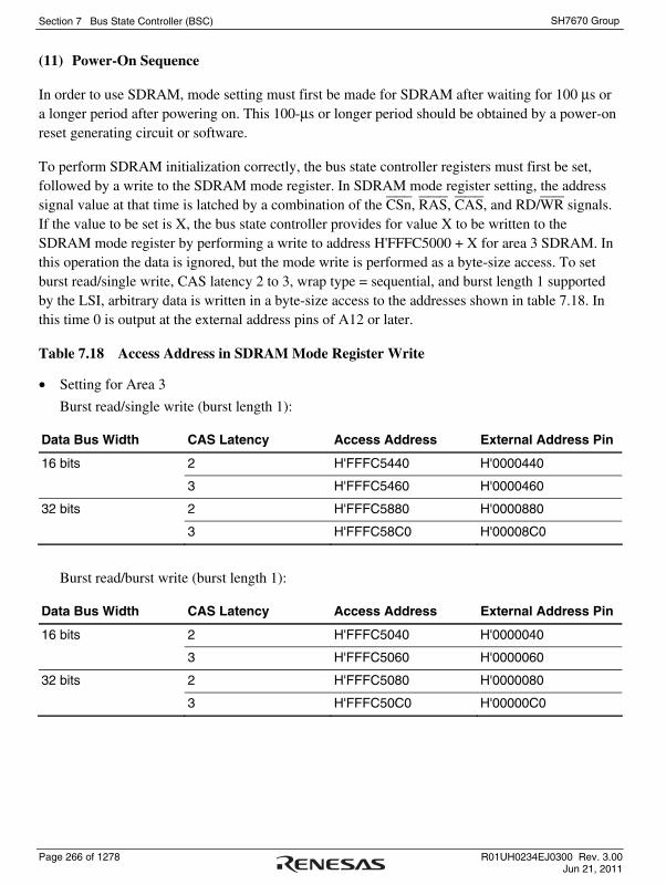
Section 7 Bus State Controller (BSC)
Page 266 of 1278 R01UH0234EJ0300 Rev. 3.00 Jun 21, 2011
SH7670 Group
(11) Power-On Sequence
In order to use SDRAM, mode setting must first be made for SDRAM after waiting for 100 μs or a longer period after powering on. This 100-μs or longer period should be obtained by a power-on reset generating circuit or software.
To perform SDRAM initialization correctly, the bus state controller registers must first be set, followed by a write to the SDRAM mode register. In SDRAM mode register setting, the address signal value at that time is latched by a combination of the CSn, RAS, CAS, and RD/WR signals. If the value to be set is X, the bus state controller provides for value X to be written to the SDRAM mode register by performing a write to address H'FFFC5000 + X for area 3 SDRAM. In this operation the data is ignored, but the mode write is performed as a byte-size access. To set burst read/single write, CAS latency 2 to 3, wrap type = sequential, and burst length 1 supported by the LSI, arbitrary data is written in a byte-size access to the addresses shown in table 7.18. In this time 0 is output at the external address pins of A12 or later.
Table 7.18 Access Address in SDRAM Mode Register Write
• Setting for Area 3
Burst read/single write (burst length 1): Data Bus Width CAS Latency Access Address External Address Pin
16 bits 2 H'FFFC5440 H'0000440
3 H'FFFC5460 H'0000460
32 bits 2 H'FFFC5880 H'0000880
3 H'FFFC58C0 H'00008C0
Burst read/burst write (burst length 1): Data Bus Width CAS Latency Access Address External Address Pin
16 bits 2 H'FFFC5040 H'0000040
3 H'FFFC5060 H'0000060
32 bits 2 H'FFFC5080 H'0000080
3 H'FFFC50C0 H'00000C0

Section 7 Bus State Controller (BSC)
R01UH0234EJ0300 Rev. 3.00 Page 267 of 1278 Jun 21, 2011
SH7670 Group
Mode register setting timing is shown in figure 7.27. A PALL command (all bank pre-charge command) is firstly issued. A REF command (auto refresh command) is then issued 8 times. An MRS command (mode register write command) is finally issued. Idle cycles, of which number is specified by the WTRP1 and WTRP0 bits in CS3WCR, are inserted between the PALL and the first REF. Idle cycles, of which number is specified by the WTRC1 and WTRC0 bits in CS3WCR, are inserted between REF and REF, and between the 8th REF and MRS. Idle cycles, of which number is one or more, are inserted between the MRS and a command to be issued next.
It is necessary to keep idle time of certain cycles for SDRAM before issuing PALL command after power-on. Refer to the manual of the SDRAM for the idle time to be needed. When the pulse width of the reset signal is longer than the idle time, mode register setting can be started immediately after the reset, but care should be taken when the pulse width of the reset signal is shorter than the idle time.
TpwTp Trr Trc Trc Tmw
Hi-Z
TnopTrc Trr TrcREF REF MRSPALL
CKIO
A25 to A0
CSn
RD/WR
RASL, RASU
DQMxx
D31 to D0
BS
DACKn*2
A12/A11*1
CASL, CASU
Notes: 1. Address pin to be connected to pin A10 of SDRAM. 2. The waveform for DACKn is when active low is specified.
Figure 7.27 SDRAM Mode Write Timing (Based on JEDEC)

Section 7 Bus State Controller (BSC)
Page 268 of 1278 R01UH0234EJ0300 Rev. 3.00 Jun 21, 2011
SH7670 Group
(12) Low-Power SDRAM
The low-power SDRAM can be accessed using the same protocol as the normal SDRAM.
The differences between the low-power SDRAM and normal SDRAM are that partial refresh takes place that puts only a part of the SDRAM in the self-refresh state during the self-refresh function, and that power consumption is low during refresh under user conditions such as the operating temperature. The partial refresh is effective in systems in which there is data in a work area other than the specific area can be lost without severe repercussions.
The low-power SDRAM supports the extension mode register (EMRS) in addition to the mode registers as the normal SDRAM. This LSI supports issuing of the EMRS command.
The EMRS command is issued according to the conditions specified in table below. For example, if data H'0YYYYYYY is written to address H'FFFC5XX0 in longword, the commands are issued to the CS3 space in the following sequence: PALL -> REF × 8 -> MRS -> EMRS. In this case, the MRS and EMRS issue addresses are H'0000XX0 and H'YYYYYYY, respectively. If data H'1YYYYYYY is written to address H'FFFC5XX0 in longword, the commands are issued to the CS3 space in the following sequence: PALL -> MRS -> EMRS.
Table 7.19 Output Addresses when EMRS Command Is Issued
Command to be Issued
Access Address
Access Data
Write Access Size
MRS Command Issue Address
EMRS Command Issue Address
CS3 MRS H'FFFC5XX0 H'******** 16 bits H'0000XX0 ⎯
CS3 MRS + EMRS
(with refresh)
H'FFFC5XX0 H'0YYYYYYY 32 bits H'0000XX0 H'YYYYYYY
CS3 MRS + EMRS
(without refresh)
H'FFFC5XX0 H'1YYYYYYY 32 bits H'0000XX0 H'YYYYYYY
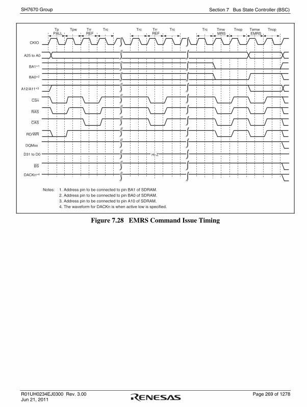
Section 7 Bus State Controller (BSC)
R01UH0234EJ0300 Rev. 3.00 Page 269 of 1278 Jun 21, 2011
SH7670 Group
CKIO
A25 to A0
CSn
RD/WR
RAS
DQMxx
D31 to D0
BS
Tpw
DACKn*4
Tp Trr
A12/A11*3
BA1*1
BA0*2
CAS
Trc Trc Tmw
Hi-Z
TnopTrc Trr TrcREF REF MRS
Temw TnopEMRSPALL
Notes: 1. Address pin to be connected to pin BA1 of SDRAM. 2. Address pin to be connected to pin BA0 of SDRAM. 3. Address pin to be connected to pin A10 of SDRAM. 4. The waveform for DACKn is when active low is specified.
Figure 7.28 EMRS Command Issue Timing

Section 7 Bus State Controller (BSC)
Page 270 of 1278 R01UH0234EJ0300 Rev. 3.00 Jun 21, 2011
SH7670 Group
• Deep power-down mode
The low-power SDRAM supports the deep power-down mode as a low-power consumption mode. In the partial self-refresh function, self-refresh is performed on a specific area. In the deep power-down mode, self-refresh will not be performed on any memory area. This mode is effective in systems where all of the system memory areas are used as work areas.
If the RMODE bit in the SDCR is set to 1 while the DEEP and RFSH bits in the SDCR are set to 1, the low-power SDRAM enters the deep power-down mode. If the RMODE bit is cleared to 0, the CKE signal is pulled high to cancel the deep power-down mode. Before executing an access after returning from the deep power-down mode, the power-up sequence must be re-executed.
TpwTp Trr Trc Trc
Hi-z
Trc
CKIO
CKE
A25 to A0
CSn
RD/WR
RAS
DQMxx
D31 to D0
BS
DACKn*2
A12/A11*1
CAS
Notes: 1. Address pin to be connected to pin A10 of SDRAM. 2. The waveform for DACKn is when active low is specified.
Figure 7.29 Deep Power-Down Mode Transition Timing

Section 7 Bus State Controller (BSC)
R01UH0234EJ0300 Rev. 3.00 Page 271 of 1278 Jun 21, 2011
SH7670 Group
7.5.6 SRAM Interface with Byte Selection
The SRAM interface with byte selection is for access to an SRAM which has a byte-selection pin (WEn). This interface has 16-bit data pins and accesses SRAMs having upper and lower byte selection pins, such as UB and LB.
When the BAS bit in CSnWCR is cleared to 0 (initial value), the write access timing of the SRAM interface with byte selection is the same as that for the normal space interface. While in read access of a byte-selection SRAM interface, the byte-selection signal is output from the WEn pin, which is different from that for the normal space interface. The basic access timing is shown in figure 7.30. In write access, data is written to the memory according to the timing of the byte-selection pin (WEn). For details, please refer to the Data Sheet for the corresponding memory.
If the BAS bit in CSnWCR is set to 1, the WEn pin and RD/WR pin timings change. Figure 7.31 shows the basic access timing. In write access, data is written to the memory according to the timing of the write enable pin (RD/WR). The data hold timing from RD/WR negation to data write must be acquired by setting the HW1 and HW0 bits in CSnWCR. Figure 7.32 shows the access timing when a software wait is specified.

Section 7 Bus State Controller (BSC)
Page 272 of 1278 R01UH0234EJ0300 Rev. 3.00 Jun 21, 2011
SH7670 Group
CKIO
A25 to A0
CSn
WEn
RD/WR
RD
RD
D31 to D0
D31 to D0
RD/WR
BS
DACKn*
Read
Write
Note: * The waveform for DACKn is when active low is specified.
T1 T2
High
Figure 7.30 Basic Access Timing for SRAM with Byte Selection (BAS = 0)

Section 7 Bus State Controller (BSC)
R01UH0234EJ0300 Rev. 3.00 Page 273 of 1278 Jun 21, 2011
SH7670 Group
T1 T2
High
CKIO
A25 to A0
CSn
WEn
RD/WR
RD
RD
D31 to D0
D31 to D0
RD/WR
BS
DACKn*
Read
Write
Note: * The waveform for DACKn is when active low is specified.
Figure 7.31 Basic Access Timing for SRAM with Byte Selection (BAS = 1)
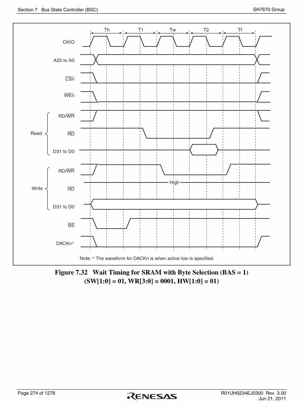
Section 7 Bus State Controller (BSC)
Page 274 of 1278 R01UH0234EJ0300 Rev. 3.00 Jun 21, 2011
SH7670 Group
T2 TfTh T1 Tw
High
CKIO
A25 to A0
CSn
WEn
RD/WR
RD
RD
D31 to D0
D31 to D0
RD/WR
BS
DACKn*
Read
Write
Note: * The waveform for DACKn is when active low is specified.
Figure 7.32 Wait Timing for SRAM with Byte Selection (BAS = 1) (SW[1:0] = 01, WR[3:0] = 0001, HW[1:0] = 01)

Section 7 Bus State Controller (BSC)
R01UH0234EJ0300 Rev. 3.00 Page 275 of 1278 Jun 21, 2011
SH7670 Group
A15
A0
CS
OE
WE
I/O15
I/O0
UB
LB
. . .
. . .
. . .
A17
A2
CSn
RD
RD/WR
D31
D16
WE3
WE2
D15
D0
WE1
WE0
This LSI
. . .
A15
A0
CS
OE
WE
I/O15
I/O0
UB
LB
. . .
. . .
. . .
64K × 16-bit SRAM
Figure 7.33 Example of Connection with 32-Bit Data-Width SRAM with Byte Selection
This LSI
A16 . . .A1
CSn
RD
RD/WR
D15 . . .D0
WE1
WE0
A15 . . .A0
CS
OE
WE
I/O 15 . . .I/O 0UB
LB
64K × 16-bit SRAM
Figure 7.34 Example of Connection with 16-Bit Data-Width SRAM with Byte Selection
Section 7 Bus State Controller (BSC)
Page 276 of 1278 R01UH0234EJ0300 Rev. 3.00 Jun 21, 2011
SH7670 Group
7.5.7 PCMCIA Interface
With this LSI, areas 5 and 6 can be used for the IC memory card and I/O card interface defined in the JEIDA specifications version 4.2 (PCMCIA2.1 Rev. 2.1) by specifying bits TYPE[2:0] in CSnBCR (n = 5 and 6) to B'101. In addition, the bits SA[1:0] in CSnWCR (n = 5 and 6) assign the upper or lower 32 Mbytes of each area to IC memory card or I/O card interface. For example, if the bits SA1 and SA0 in CS5WCR are set to 1 and cleared to 0, respectively, the upper 32 Mbytes of area 5 are used for IC memory card interface and the lower 32 Mbytes are used for I/O card interface.
When the PCMCIA interface is used, the bus size must be specified as 8 bits or 16 bits using the bits BSZ[1:0] in CS5BCR or CS6BCR.
Figure 7.35 shows an example of connection between this LSI and a PCMCIA card. To enable hot swapping (insertion and removal of the PCMCIA card with the system power turned on), tri-state buffers must be connected between the LSI and the PCMCIA card.
In the JEIDA and PCMCIA standards, operation in big endian mode is not clearly defined. Consequently, the provided PCMCIA interface in big endian mode is available only for this LSI.

Section 7 Bus State Controller (BSC)
R01UH0234EJ0300 Rev. 3.00 Page 277 of 1278 Jun 21, 2011
SH7670 Group
This LSIPC card
(memory or I/O)
A25 to A0
D7 to D0
CE1
CE2
OE
WE/PGM
IORD
IOWR
REG
A25 to A0
D7 to D0
D15 to D8
RD/WR
CS5B/CE1A
CE2A
RD
WE1/WE
WE2/ICIORD
WE3/ICIOWR
REG (Output port)
WAIT
IOIS16
G
GDIR
G
G
DIR
D15 to D8
WAIT
IOIS16
CD1, CD2Carddetector
Figure 7.35 Example of PCMCIA Interface Connection

Section 7 Bus State Controller (BSC)
Page 278 of 1278 R01UH0234EJ0300 Rev. 3.00 Jun 21, 2011
SH7670 Group
(1) Basic Timing for Memory Card Interface
Figure 7.36 shows the basic timing of the PCMCIA IC memory card interface. When areas 5 and 6 are specified as the PCMCIA interface, the bus is accessed with the IC memory card interface according to the SA[1:0] bit settings in CS5WCR and CS6WCR. If the external bus frequency (CKIO) increases, the setup times and hold times for the address pins (A25 to A0), card enable signals (CE1A, CE2A, CE1B, CE2B), and write data (D15 to D0) to the RD and WE signals become insufficient. To prevent this error, this LSI enables the setup times and hold times for areas 5 and 6 to be specified independently, using CS5WCR and CS6WCR. In the PCMCIA interface, as in the normal space interface, a software wait or hardware wait using the WAIT pin can be inserted. Figure 7.37 shows the PCMCIA memory bus wait timing.
Tpcm1w
CKIO
A25 to A0
CExx
RD/WR
RD
D15 to D0
WE
D15 to D0
BS
Read
Write
Tpcm2Tpcm1 Tpcm1w Tpcm1w
Figure 7.36 Basic Access Timing for PCMCIA Memory Card Interface

Section 7 Bus State Controller (BSC)
R01UH0234EJ0300 Rev. 3.00 Page 279 of 1278 Jun 21, 2011
SH7670 Group
Tpcm1w
CKIO
A25 to A0
CExx
RD/WR
RD
D15 to D0
WE
D15 to D0
BS
Read
Write
Tpcm2Tpcm0 Tpcm1 Tpcm1wTpcm0w Tpcm2wTpcm1w Tpcm1w
WAIT
Figure 7.37 Wait Timing for PCMCIA Memory Card Interface (TED[3:0] = B'0010, PCW[3:0] = B'0000, TEH[3:0] = B'0001, Hardware Wait = 1)
A port is used to generate the REG signal that switches between the common memory and attribute memory. As shown in the example in figure 7.38, when the total memory space necessary for the common memory and attribute memory is 32 Mbytes or less, pin A24 can be used as the REG signal to allocate a 16-Mbyte common memory space and a 16-Mbyte attribute memory space.

Section 7 Bus State Controller (BSC)
Page 280 of 1278 R01UH0234EJ0300 Rev. 3.00 Jun 21, 2011
SH7670 Group
In case of 32Mbyts capacity (REG = I/O port is used)
Area 5: H'14000000Attribute memory/Common memory
I/O Space
Attribute memory/Common memory
I/O Space
Area 5: H'16000000
Area 6: H'18000000
Area 6: H'1A000000
In case of 16Mbyts capacity (REG = A24 is used)
Area 5: H'14000000Attribute memory
I/OSpace
Area 5: H'15000000
Area 5: H'16000000
H'17000000
Area 6: H'18000000
Area 6: H'19000000
Area 6: H'1A000000
H'1B000000
Common memory
Attribute memory
I/OSpace
Common memory
Figure 7.38 Example of PCMCIA Space Allocation (CS5WCR.SA[1:0] = B'10, CS6WCR.SA[1:0] = B'10)

Section 7 Bus State Controller (BSC)
R01UH0234EJ0300 Rev. 3.00 Page 281 of 1278 Jun 21, 2011
SH7670 Group
(2) Basic Timing for I/O Card Interface
Figures 7.39 and 7.40 show the basic timing for the PCMCIA I/O card interface.
When accessing an I/O card through the PCMCIA interface, be sure to access the space as cache-disabled.
Switching between I/O card and IC memory card interfaces in the respective address spaces is accomplished by the SA[1:0] bit settings in CS5WCR and CS6WCR.
The IOIS16 pin can be used for dynamic adjustment of the width of the I/O bus in access to an I/O card via the PCMCIA interface when little endian mode has been selected. When the bus width of area 5 or 6 is set to 16 bits and the IOIS16 signal is driven high during a cycle of word-unit access to the I/O card bus, the bus width will be recognized as 8 bits and only 8 bits of data will be accessed during the current cycle of the I/O card bus. Operation will automatically continue with access to the remaining 8 bits of data.
The IOIS16 signal is sampled on falling edges of the CKIO in Tpci0 as well as all Tpci0w cycles for which the TED3 to TED0 bits are set to 1.5 cycles or more, and the CE2A and CE2B signals are updated after 1.5 cycles of the CKIO signal from the sampling point of Tpci0. Ensure that the IOIS16 signal is defined at all sampling points and does not change along the way.
Set the TED3 to TED0 bits to satisfy the requirement of the PC card in use with regard to setup timing from ICIORD or ICIOWR to CE1 or CE2.
The basic waveforms for dynamic bus-size adjustment are shown in figure 7.40.
Since the IOIS16 signal is not supported in big endian mode, the IOIS16 signal should be fixed to the low level when big endian mode has been selected.

Section 7 Bus State Controller (BSC)
Page 282 of 1278 R01UH0234EJ0300 Rev. 3.00 Jun 21, 2011
SH7670 Group
Tpci1w
CKIO
A25 to A0
CExx
RD/WR
ICIORD
D15 to D0
ICIOWR
D15 to D0
BS
Read
Write
Tpci2Tpci1 Tpci1w Tpci1w
Figure 7.39 Basic Access Timing for PCMCIA I/O Card Interface
Tpci1w
CKIO
A25 to A0
CE1x
RD/WR
ICIORD
D15 to D0
ICIOWR
IOIS16
D15 to D0
BS
Read
Write
Tpci2
CE2x
Tpci0 Tpci1 Tpci1wTpci0w Tpci2wTpci1w Tpci1w
WAIT
Tpci1w Tpci2Tpci0 Tpci1 Tpci1wTpci0w Tpci2wTpci1w Tpci1w
Figure 7.40 Dynamic Bus-Size Adjustment Timing for PCMCIA I/O Card Interface (TED[3:0] = B'0010, PCW[3:0] = B'0000, TEH[3:0] = B'0001, Hardware Wait = 1)
Section 7 Bus State Controller (BSC)
R01UH0234EJ0300 Rev. 3.00 Page 283 of 1278 Jun 21, 2011
SH7670 Group
7.5.8 Wait between Access Cycles
As the operating frequency of LSIs becomes higher, the off-operation of the data buffer often collides with the next data access when the read operation from devices with slow access speed is completed. As a result of these collisions, the reliability of the device is low and malfunctions may occur. A function that avoids data collisions by inserting idle (wait) cycles between continuous access cycles has been newly added.
The number of wait cycles between access cycles can be set by the WM bit in CSnWCR, bits IWW2 to IWW0, IWRWD2 to IWRWD0, IWRWS2 to IWRWS0, IWRRD2 to IWRRD0, and IWRRS2 to IWRRS 0 in CSnBCR, and bits DMAIW2 to DMAIW0 and DMAIWA in CMNCR. The conditions for setting the idle cycles between access cycles are shown below.
1. Continuous access cycles are write-read or write-write
2. Continuous access cycles are read-write for different spaces
3. Continuous access cycles are read-write for the same space
4. Continuous access cycles are read-read for different spaces
5. Continuous access cycles are read-read for the same space
6. Data output from an external device caused by DMA single address transfer is followed by data output from another device that includes this LSI (DMAIWA = 0)
7. Data output from an external device caused by DMA single address transfer is followed by any type of access (DMAIWA = 1)
For the specification of the number of idle cycles between access cycles described above, refer to the description of each register.
Besides the idle cycles between access cycles specified by the registers, idle cycles must be inserted to interface with the internal bus or to obtain the minimum pulse width for a multiplexed pin (WEn). The following gives detailed information about the idle cycles and describes how to estimate the number of idle cycles.
The number of idle cycles on the external bus from CSn negation to CSn or CSm assertion is described below. Here, CSn and CSm also include CE2A and CE2B for PCMCIA.
There are eight conditions that determine the number of idle cycles on the external bus as shown in table 7.20. The effects of these conditions are shown in figure 7.41.

Section 7 Bus State Controller (BSC)
Page 284 of 1278 R01UH0234EJ0300 Rev. 3.00 Jun 21, 2011
SH7670 Group
Table 7.20 Conditions for Determining Number of Idle Cycles
No. Condition Description Range Note
[1] DMAIW[2:0] in CMNCR
These bits specify the number of idle cycles for DMA single address transfer. This condition is effective only for single address transfer and generates idle cycles after the access is completed.
0 to 12 When 0 is specified for the number of idle cycles, the DACK signal may be asserted continuously. This causes a discrepancy between the number of cycles detected by the device with DACK and the DMAC transfer count, resulting in a malfunction.
[2] IW***[2:0] in CSnBCR
These bits specify the number of idle cycles for access other than single address transfer. The number of idle cycles can be specified independently for each combination of the previous and next cycles. For example, in the case where reading CS3 space followed by reading other CS space, the bits IWRRD[2:0] in CS3BCR should be set to B'100 to specify six or more idle cycles. This condition is effective only for access cycles other than single address transfer and generates idle cycles after the access is completed.
0 to 12 Do not set 0 for the number of idle cycles between memory types which are not allowed to be accessed successively.
[3] SDRAM-related bits in CSnWCR
These bits specify precharge completion and startup wait cycles and idle cycles between commands for SDRAM access. This condition is effective only for SDRAM access and generates idle cycles after the access is completed
0 to 3 Specify these bits in accordance with the specification of the target SDRAM.
[4] WM in CSnWCR
This bit enables or disables external WAIT pin input for the memory types other than SDRAM. When this bit is cleared to 0 (external WAIT enabled), one idle cycle is inserted to check the external WAIT pin input after the access is completed. When this bit is set to 1 (disabled), no idle cycle is generated.
0 or 1
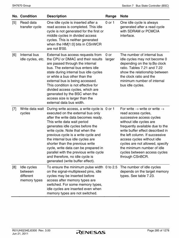
Section 7 Bus State Controller (BSC)
R01UH0234EJ0300 Rev. 3.00 Page 285 of 1278 Jun 21, 2011
SH7670 Group
No. Condition Description Range Note
[5] Read data transfer cycle
One idle cycle is inserted after a read access is completed. This idle cycle is not generated for the first or middle cycles in divided access cycles. This is neither generated when the HM[1:0] bits in CSnWCR are not B'00.
0 or 1 One idle cycle is always generated after a read cycle with SDRAM or PCMCIA interface.
[6] Internal bus idle cycles, etc.
External bus access requests from the CPU or DMAC and their results are passed through the internal bus. The external bus enters idle state during internal bus idle cycles or while a bus other than the external bus is being accessed. This condition is not effective for divided access cycles, which are generated by the BSC when the access size is larger than the external data bus width.
0 or larger
The number of internal bus idle cycles may not become 0 depending on the Iφ:Bφ clock ratio. Tables 7.21 and 7.22 show the relationship between the clock ratio and the minimum number of internal bus idle cycles.
[7] Write data wait cycles
During write access, a write cycle is executed on the external bus only after the write data becomes ready. This write data wait period generates idle cycles before the write cycle. Note that when the previous cycle is a write cycle and the internal bus idle cycles are shorter than the previous write cycle, write data can be prepared in parallel with the previous write cycle and therefore, no idle cycle is generated (write buffer effect).
0 or 1 For write → write or write → read access cycles, successive access cycles without idle cycles are frequently available due to the write buffer effect described in the left column. If successive access cycles without idle cycles are not allowed, specify the minimum number of idle cycles between access cycles through CSnBCR.
[8] Idle cycles between different memory types
To ensure the minimum pulse width on the signal-multiplexed pins, idle cycles may be inserted before access after memory types are switched. For some memory types, idle cycles are inserted even when memory types are not switched.
0 to 2.5 The number of idle cycles depends on the target memory types. See table 7.23.

Section 7 Bus State Controller (BSC)
Page 286 of 1278 R01UH0234EJ0300 Rev. 3.00 Jun 21, 2011
SH7670 Group
In the above conditions, a total of four conditions, that is, condition [1] or [2] (either one is effective), condition [3] or [4] (either one is effective), a set of conditions [5] to [7] (these are generated successively, and therefore the sum of them should be taken as one set of idle cycles), and condition [8] are generated at the same time. The maximum number of idle cycles among these four conditions become the number of idle cycles on the external bus. To ensure the minimum idle cycles, be sure to make register settings for condition [1] or [2].
CKIO
CSn
Previous access External bus idle cycles
Idle cycle after access
Either one of themis effective
[1]DMAIW[2:0] setting in CMNCR
[2] IWW[2:0] setting in CSnBCRIWRWD[2:0] setting in CSnBCRIWRWS[2:0] setting in CSnBCRIWRRD[2:0] setting in CSnBCRIWRRS[2:0] setting in CSnBCR
[3]WTRP[1:0] setting in CSnWCRTRWL[1:0] setting in CSnWCRWTRC[1:0] setting in CSnWCR
[4]WM setting in CSnWCR
[6] Internal bus idle cycles, etc.
[8] Idle cyclesbetweendifferentmemory types
[5]Readdatatransfer
[7] Writedatawait
Idle cycle before access
Next access
Condition [1] or [2]
A total of four conditions (condition [1] or [2], condition [3] or [4], a set of conditions [5] to [7], and condition [8]) generate idle cycle at the same time. Accordingly, the maximum number of cycles among these four conditions become the number of idle cycles.
Note:
Condition [8]
Condition [3] or [4]
Set of conditions[5] to [7]
Either one of themis effective
Figure 7.41 Idle Cycle Conditions

Section 7 Bus State Controller (BSC)
R01UH0234EJ0300 Rev. 3.00 Page 287 of 1278 Jun 21, 2011
SH7670 Group
Table 7.21 Minimum Number of Idle Cycles on Internal Bus (CPU Operation)
Clock Ratio (Iφ:Bφ)
CPU Operation 8:1 6:1 4:1 3:1 2:1 1:1
Write → write 1 1 2 2 2 3
Write → read 0 0 0 0 0 1
Read → write 1 1 2 2 2 3
Read → read 0 0 0 0 0 1
Table 7.22 Minimum Number of Idle Cycles on Internal Bus (DMAC Operation)
Transfer Mode
DMAC Operation Dual Address Single Address
Write → write 0 2
Write → read 0 or 2 0
Read → write 0 0
Read → read 0 2
Notes: 1. The write → write and read → read columns in dual address transfer indicate the cycles in the divided access cycles.
2. For the write → read cycles in dual address transfer, 0 means different channels are activated successively and 2 means when the same channel is activated successively.
3. The write → read and read → write columns in single address transfer indicate the case when different channels are activated successively. The "write" means transfer from a device with DACK to external memory and the "read" means transfer from external memory to a device with DACK.
Table 7.23 Number of Idle Cycles Inserted between Access Cycles to Different Memory Types
Next Cycle
Previous Cycle SRAM Byte SRAM (BAS = 0) Byte SRAM (BAS = 1) SDRAM PCMCIA
SRAM 0 0 1 1 0
Byte SRAM (BAS = 0) 0 0 1 1 0
Byte SRAM (BAS = 1) 1 1 0 0 1
SDRAM 1 1 0 0 1
PCMCIA 0 0 1 1 0

Section 7 Bus State Controller (BSC)
Page 288 of 1278 R01UH0234EJ0300 Rev. 3.00 Jun 21, 2011
SH7670 Group
Figure 7.42 shows sample estimation of idle cycles between access cycles. In the actual operation, the idle cycles may become shorter than the estimated value due to the write buffer effect or may become longer due to internal bus idle cycles caused by stalling in the pipeline due to CPU instruction execution or CPU register conflicts. Please consider these errors when estimating the idle cycles.
Sample estimation of the number of idle clock cycles (states) between cycles of bus access
• Condition
Item NoteR→R R→W W→W W→R
0 0 0 0
0 0 0 0
1 1 0 0
0 2 2 0
0 1 0 0
1 4 2 0
0 0 0 0
1 4 2 0
1
(1)/(2)
(3)/(4)
(5)
(6)
(7)
(5)+(6)+(7)
(8)
Estimated numberof idle cycles
Actual number of idle cycles
Since CSnBCR is set to 0
When the WM bit is set to 1
Generated after the read cycle
See the description for Iφ:Bφ = 4:1 in table 7.21.
The effect of the write buffer is that idle cycles are not generated the second time.
Due to SRAM→SRAM
Maximum value among (1)/(2), (3)/(4), (5)+(6)+(7), and (8)
The mismatch in the case of W→R is because the estimate of the number of idle cycles for item (6) was zero. Since a loop-decision instruction is actually executed here, an idle cycle is generated internally.
4 2 1
0 is specified as the number of idle cycles between CS5BCR and CS6BCR.WM bit in CS5WCR and CS6WCR = 1 (external WAIT_ pin disabled)HW[1:0] = 00 (no delay of CS negation)Iφ:Bφ = 4:1No other processing proceeds during the transfer.CS5 and CS6 are connected to SRAM for access in 32-bit units by a 32-bit-wide bus.
We consider CPU access for the transfer of data from the CS5 to the CS6 space. For this transfer, the sequence read from CS5 →read from CS5 →write to CS6→write to CS6 ... is repeated.
The items that decide the number of idle cycles are estimated for the different transitions on between bus cycles.R indicates reading and W indicates writing in the table below.
Figure 7.42 Comparison between Estimated Idle Cycles and Actual Value

Section 7 Bus State Controller (BSC)
R01UH0234EJ0300 Rev. 3.00 Page 289 of 1278 Jun 21, 2011
SH7670 Group
7.5.9 Others
(1) Reset
The bus state controller (BSC) can be initialized completely only at power-on reset. At power-on reset, all signals are negated and data output buffers are turned off regardless of the bus cycle state after the internal reset is synchronized with the internal clock. All control registers are initialized. In standby, sleep, and manual reset, control registers of the bus state controller are not initialized. At manual reset, only the current bus cycle being executed is completed. Since the RTCNT continues counting up during manual reset signal assertion, a refresh request occurs to initiate the refresh cycle.
(2) Access from the Side of the LSI Internal Bus Master
There are three types of LSI internal buses: a CPU bus, internal bus, and peripheral bus. The CPU and cache memory are connected to the CPU bus. Internal bus masters other than the CPU and bus state controller are connected to the internal bus. Low-speed peripheral modules are connected to the peripheral bus. Internal memories other than the cache memory are connected bidirectionally to the CPU bus and internal bus. Access from the CPU bus to the internal bus is enabled but access from the internal bus to the cache bus is disabled. This gives rise to the following problems.
On-chip bus masters such as DMAC other than the CPU can access internal memory other than the cache memory but cannot access the cache memory. If an on-chip bus master other than the CPU writes data to an external memory other than the cache, the contents of the external memory may differ from that of the cache memory. To prevent this problem, if the external memory whose contents is cached is written by an on-chip bus master other than the CPU, the corresponding cache memory should be purged by software.
In a cache-enabled space, if the CPU initiates read access, the cache is searched. If the cache stores data, the CPU latches the data and completes the read access. If the cache does not store data, the CPU performs four contiguous longword read cycles to perform cache fill operations via the internal bus. If a cache miss occurs in byte or word operand access or at a branch to an odd word boundary (4n + 2), the CPU performs four contiguous longword access cycles to perform a cache fill operation on the external interface. For a cache-disabled space, the CPU performs access according to the actual access addresses. For an instruction fetch to an even word boundary (4n), the CPU performs longword access. For an instruction fetch to an odd word boundary (4n + 2), the CPU performs word access.
For a read cycle of an on-chip peripheral module, the cycle is initiated through the internal bus and peripheral bus. The read data is sent to the CPU via the peripheral bus, internal bus, and CPU bus.
Section 7 Bus State Controller (BSC)
Page 290 of 1278 R01UH0234EJ0300 Rev. 3.00 Jun 21, 2011
SH7670 Group
In a write cycle for the cache-enabled space, the write cycle operation differs according to the cache write methods.
In write-back mode, the cache is first searched. If data is detected at the address corresponding to the cache, the data is then re-written to the cache. In the actual memory, data will not be re-written until data in the corresponding address is re-written. If data is not detected at the address corresponding to the cache, the cache is modified. In this case, data to be modified is first saved to the internal buffer, 16-byte data including the data corresponding to the address is then read, and data in the corresponding access of the cache is finally modified. Following these operations, a write-back cycle for the saved 16-byte data is executed.
In write-through mode, the cache is first searched. If data is detected at the address corresponding to the cache, the data is re-written to the cache simultaneously with the actual write via the internal bus. If data is not detected at the address corresponding to the cache, the cache is not modified but an actual write is performed via the internal bus.
Since the bus state controller (BSC) incorporates a one-stage write buffer, the BSC can execute an access via the internal bus before the previous external bus cycle is completed in a write cycle. If the on-chip module is read or written after the external low-speed memory is written, the on-chip module can be accessed before the completion of the external low-speed memory write cycle.
In read cycles, the CPU is placed in the wait state until read operation has been completed. To continue the process after the data write to the device has been completed, perform a dummy read to the same address to check for completion of the write before the next process to be executed.
The write buffer of the BSC functions in the same way for an access by a bus master other than the CPU such as the DMAC. Accordingly, to perform dual address DMA transfers, the next read cycle is initiated before the previous write cycle is completed. Note, however, that if both the DMA source and destination addresses exist in external memory space, the next write cycle will not be initiated until the previous write cycle is completed.
Changing the registers in the BSC while the write buffer is operating may disrupt correct write access. Therefore, do not change the registers in the BSC immediately after a write access. If this change becomes necessary, do it after executing a dummy read of the write data.
In this LSI, the priority level applicable when there is a request for bus mastership for the internal bus from any of the internal bus masters excluding the CPU (that is, A-DMAC (including F-DMAC), E-DMAC, and DMAC) can be set in the register.
When changing the priority level, rewrite the register after making sure that none of the A-DMAC (including F-DMAC), E-DMAC, and DMAC is started.

Section 7 Bus State Controller (BSC)
R01UH0234EJ0300 Rev. 3.00 Page 291 of 1278 Jun 21, 2011
SH7670 Group
(3) On-Chip Peripheral Module Access
To access an on-chip module register, two or more peripheral module clock (Pφ) cycles are required. Care must be taken in system design.
When the CPU writes data to the internal peripheral registers, the CPU performs the succeeding instructions without waiting for the completion of writing to registers.
For example, a case is described here in which the system is transferring to the software standby mode for power savings. To make this transition, the SLEEP instruction must be performed after setting the STBY bit in the STBCR register to 1. However a dummy read of the STBCR register is required before executing the SLEEP instruction. If a dummy read is omitted, the CPU executes the SLEEP instruction before the STBY bit is set to 1, thus the system enters sleep mode not software standby mode. A dummy read of the STBCR register is indispensable to complete writing to the STBY bit.
To reflect the change by internal peripheral registers while performing the succeeding instructions, execute a dummy read of registers to which write instruction is given and then perform the succeeding instructions.

Section 7 Bus State Controller (BSC)
Page 292 of 1278 R01UH0234EJ0300 Rev. 3.00 Jun 21, 2011
SH7670 Group

Section 8 Direct Memory Access Controller (DMAC)
R01UH0234EJ0300 Rev. 3.00 Page 293 of 1278 Jun 21, 2011
SH7670 Group
Section 8 Direct Memory Access Controller (DMAC)
The DMAC can be used in place of the CPU to perform high-speed transfers between external devices that have DACK (transfer request acknowledge signal), external memory, on-chip memory, memory-mapped external devices, and on-chip peripheral modules.
8.1 Features
• Number of channels: Eight channels (channels 0 to 7) selectable
Two channels (channels 0 and 1) can receive external requests.
• 4-Gbyte physical address space
• Data transfer unit is selectable: Byte, word (two bytes), longword (four bytes), and 16 bytes (longword × 4)
• Maximum transfer count: 16,777,216 transfers (24 bits)
• Address mode: Dual address mode and single address mode are supported.
• Transfer requests
⎯ External request
⎯ On-chip peripheral module request
⎯ Auto request
The following modules can issue on-chip peripheral module requests.
⎯ Six SCIF sources, two IIC3 sources, two CMT sources, two SSI sources, and two SDHI sources
• Selectable bus modes
⎯ Cycle steal mode (normal mode and intermittent mode)
⎯ Burst mode
• Selectable channel priority levels: The channel priority levels are selectable between fixed mode and round-robin mode.
• Interrupt request: An interrupt request can be sent to the CPU on completion of half- or full-data transfer. Through the HE and HIE bits in CHCR, an interrupt is specified to be issued to the CPU when half of the initially specified DMA transfer is completed.
• External request detection: There are following four types of DREQ input detection.
⎯ Low level detection
⎯ High level detection
⎯ Rising edge detection
⎯ Falling edge detection

Section 8 Direct Memory Access Controller (DMAC)
Page 294 of 1278 R01UH0234EJ0300 Rev. 3.00 Jun 21, 2011
SH7670 Group
• Transfer request acknowledge and transfer end signals: Active levels for DACK and TEND can be set independently.
• Support of reload functions in DMA transfer information registers: DMA transfer using the same information as the current transfer can be repeated automatically without specifying the information again. Modifying the reload registers during DMA transfer enables next DMA transfer to be done using different transfer information.
The reload function can be enabled or disabled in each channel and in each reload register.
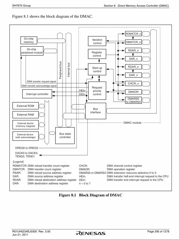
Section 8 Direct Memory Access Controller (DMAC)
R01UH0234EJ0300 Rev. 3.00 Page 295 of 1278 Jun 21, 2011
SH7670 Group
Figure 8.1 shows the block diagram of the DMAC.
On-chip peripheral module
DMA transfer request signal
DMA transfer acknowledge signal
Per
iphe
ral b
us
Inte
rnal
bus
External ROM
On-chipmemory
Interrupt controller
DREQ0 to DREQ3
HEIn
DACK0 to DACK3,TEND0, TEND1
External RAM
Businterface
Bus statecontroller
External device(memory mapped)
External device (with acknowledge)
Requestprioritycontrol
Start-upcontrol
Registercontrol
Iterationcontrol
RDMATCR_n
DMATCR_n
RSAR_n
SAR_n
DAR_n
RDAR_n
CHCR_n
DMAOR
DMARS0to DMARS3
RDMATCR:DMATCR:RSAR:SAR:RDAR:DAR:
DMA reload transfer count registerDMA transfer count registerDMA reload source address registerDMA source address registerDMA reload destination address registerDMA destination address register
CHCR:DMAOR:DMARS0 to DMARS3:HEIn:DEIn:n = 0 to 7
DMA channel control registerDMA operation registerDMA extension resource selectors 0 to 3DMA transfer half-end interrupt request to the CPUDMA transfer end interrupt request to the CPU
DEIn
[Legend]
DMAC module
Figure 8.1 Block Diagram of DMAC

Section 8 Direct Memory Access Controller (DMAC)
Page 296 of 1278 R01UH0234EJ0300 Rev. 3.00 Jun 21, 2011
SH7670 Group
8.2 Input/Output Pins
The external pins for DMAC are described below. Table 8.1 lists the configuration of the pins that are connected to external bus. DMAC has pins for two channels (channels 0 and 1) for external bus use.
Table 8.1 Pin Configuration
Channel Name Abbreviation I/O Function
DMA transfer request DREQ0 I DMA transfer request input from an external device to channel 0
0
DMA transfer request acknowledge
DACK0 O DMA transfer request acknowledge output from channel 0 to an external device
DMA transfer request DREQ1 I DMA transfer request input from an external device to channel 1
1
DMA transfer request acknowledge
DACK1 O DMA transfer request acknowledge output from channel 1 to an external device
0 DMA transfer end TEND0 O DMA transfer end output for channel 0
1 DMA transfer end TEND1 O DMA transfer end output for channel 1
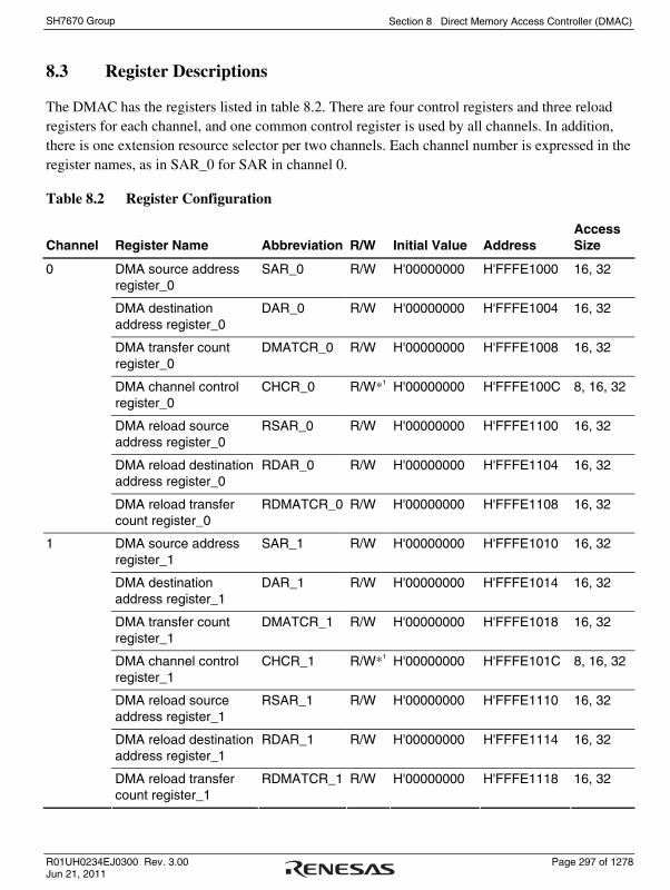
Section 8 Direct Memory Access Controller (DMAC)
R01UH0234EJ0300 Rev. 3.00 Page 297 of 1278 Jun 21, 2011
SH7670 Group
8.3 Register Descriptions
The DMAC has the registers listed in table 8.2. There are four control registers and three reload registers for each channel, and one common control register is used by all channels. In addition, there is one extension resource selector per two channels. Each channel number is expressed in the register names, as in SAR_0 for SAR in channel 0.
Table 8.2 Register Configuration
Channel Register Name Abbreviation R/W Initial Value Address Access Size
DMA source address register_0
SAR_0 R/W H'00000000 H'FFFE1000 16, 32
DMA destination address register_0
DAR_0 R/W H'00000000 H'FFFE1004 16, 32
DMA transfer count register_0
DMATCR_0 R/W H'00000000 H'FFFE1008 16, 32
DMA channel control register_0
CHCR_0 R/W*1 H'00000000 H'FFFE100C 8, 16, 32
DMA reload source address register_0
RSAR_0 R/W H'00000000 H'FFFE1100 16, 32
DMA reload destination address register_0
RDAR_0 R/W H'00000000 H'FFFE1104 16, 32
0
DMA reload transfer count register_0
RDMATCR_0 R/W H'00000000 H'FFFE1108 16, 32
DMA source address register_1
SAR_1 R/W H'00000000 H'FFFE1010 16, 32
DMA destination address register_1
DAR_1 R/W H'00000000 H'FFFE1014 16, 32
DMA transfer count register_1
DMATCR_1 R/W H'00000000 H'FFFE1018 16, 32
DMA channel control register_1
CHCR_1 R/W*1 H'00000000 H'FFFE101C 8, 16, 32
DMA reload source address register_1
RSAR_1 R/W H'00000000 H'FFFE1110 16, 32
DMA reload destination address register_1
RDAR_1 R/W H'00000000 H'FFFE1114 16, 32
1
DMA reload transfer count register_1
RDMATCR_1 R/W H'00000000 H'FFFE1118 16, 32

Section 8 Direct Memory Access Controller (DMAC)
Page 298 of 1278 R01UH0234EJ0300 Rev. 3.00 Jun 21, 2011
SH7670 Group
Channel Register Name Abbreviation R/W Initial Value Address Access Size
DMA source address register_2
SAR_2 R/W H'00000000 H'FFFE1020 16, 32
DMA destination address register_2
DAR_2 R/W H'00000000 H'FFFE1024 16, 32
DMA transfer count register_2
DMATCR_2 R/W H'00000000 H'FFFE1028 16, 32
DMA channel control register_2
CHCR_2 R/W*1 H'00000000 H'FFFE102C 8, 16, 32
DMA reload source address register_2
RSAR_2 R/W H'00000000 H'FFFE1120 16, 32
DMA reload destination address register_2
RDAR_2 R/W H'00000000 H'FFFE1124 16, 32
2
DMA reload transfer count register_2
RDMATCR_2 R/W H'00000000 H'FFFE1128 16, 32
DMA source address register_3
SAR_3 R/W H'00000000 H'FFFE1030 16, 32
DMA destination address register_3
DAR_3 R/W H'00000000 H'FFFE1034 16, 32
DMA transfer count register_3
DMATCR_3 R/W H'00000000 H'FFFE1038 16, 32
DMA channel control register_3
CHCR_3 R/W*1 H'00000000 H'FFFE103C 8, 16, 32
DMA reload source address register_3
RSAR_3 R/W H'00000000 H'FFFE1130 16, 32
DMA reload destination address register_3
RDAR_3 R/W H'00000000 H'FFFE1134 16, 32
3
DMA reload transfer count register_3
RDMATCR_3 R/W H'00000000 H'FFFE1138 16, 32

Section 8 Direct Memory Access Controller (DMAC)
R01UH0234EJ0300 Rev. 3.00 Page 299 of 1278 Jun 21, 2011
SH7670 Group
Channel Register Name Abbreviation R/W Initial Value Address Access Size
DMA source address register_4
SAR_4 R/W H'00000000 H'FFFE1040 16, 32
DMA destination address register_4
DAR_4 R/W H'00000000 H'FFFE1044 16, 32
DMA transfer count register_4
DMATCR_4 R/W H'00000000 H'FFFE1048 16, 32
DMA channel control register_4
CHCR_4 R/W*1 H'00000000 H'FFFE104C 8, 16, 32
DMA reload source address register_4
RSAR_4 R/W H'00000000 H'FFFE1140 16, 32
DMA reload destination address register_4
RDAR_4 R/W H'00000000 H'FFFE1144 16, 32
4
DMA reload transfer count register_4
RDMATCR_4 R/W H'00000000 H'FFFE1148 16, 32
DMA source address register_5
SAR_5 R/W H'00000000 H'FFFE1050 16, 32
DMA destination address register_5
DAR_5 R/W H'00000000 H'FFFE1054 16, 32
DMA transfer count register_5
DMATCR_5 R/W H'00000000 H'FFFE1058 16, 32
DMA channel control register_5
CHCR_5 R/W*1 H'00000000 H'FFFE105C 8, 16, 32
DMA reload source address register_5
RSAR_5 R/W H'00000000 H'FFFE1150 16, 32
DMA reload destination address register_5
RDAR_5 R/W H'00000000 H'FFFE1154 16, 32
5
DMA reload transfer count register_5
RDMATCR_5 R/W H'00000000 H'FFFE1158 16, 32

Section 8 Direct Memory Access Controller (DMAC)
Page 300 of 1278 R01UH0234EJ0300 Rev. 3.00 Jun 21, 2011
SH7670 Group
Channel Register Name Abbreviation R/W Initial Value Address Access Size
DMA source address register_6
SAR_6 R/W H'00000000 H'FFFE1060 16, 32
DMA destination address register_6
DAR_6 R/W H'00000000 H'FFFE1064 16, 32
DMA transfer count register_6
DMATCR_6 R/W H'00000000 H'FFFE1068 16, 32
DMA channel control register_6
CHCR_6 R/W*1 H'00000000 H'FFFE106C 8, 16, 32
DMA reload source address register_6
RSAR_6 R/W H'00000000 H'FFFE1160 16, 32
DMA reload destination address register_6
RDAR_6 R/W H'00000000 H'FFFE1164 16, 32
6
DMA reload transfer count register_6
RDMATCR_6 R/W H'00000000 H'FFFE1168 16, 32
DMA source address register_7
SAR_7 R/W H'00000000 H'FFFE1070 16, 32
DMA destination address register_7
DAR_7 R/W H'00000000 H'FFFE1074 16, 32
DMA transfer count register_7
DMATCR_7 R/W H'00000000 H'FFFE1078 16, 32
DMA channel control register_7
CHCR_7 R/W*1 H'00000000 H'FFFE107C 8, 16, 32
DMA reload source address register_7
RSAR_7 R/W H'00000000 H'FFFE1170 16, 32
DMA reload destination address register_7
RDAR_7 R/W H'00000000 H'FFFE1174 16, 32
7
DMA reload transfer count register_7
RDMATCR_7 R/W H'00000000 H'FFFE1178 16, 32

Section 8 Direct Memory Access Controller (DMAC)
R01UH0234EJ0300 Rev. 3.00 Page 301 of 1278 Jun 21, 2011
SH7670 Group
Channel Register Name Abbreviation R/W Initial Value Address Access Size
Common DMA operation register DMAOR R/W*2 H'0000 H'FFFE1200 8, 16
0 and 1 DMA extension resource selector 0
DMARS0 R/W H'0000 H'FFFE1300 16
2 and 3 DMA extension resource selector 1
DMARS1 R/W H'0000 H'FFFE1304 16
4 and 5 DMA extension resource selector 2
DMARS2 R/W H'0000 H'FFFE1308 16
6 and 7 DMA extension resource selector 3
DMARS3 R/W H'0000 H'FFFE130C 16
Notes: 1. For the HE and TE bits in CHCRn, only 0 can be written to clear the flags after 1 is read.
2. For the AE and NMIF bits in DMAOR, only 0 can be written to clear the flags after 1 is read.
8.3.1 DMA Source Address Registers (SAR)
The DMA source address registers (SAR) are 32-bit readable/writable registers that specify the source address of a DMA transfer. During a DMA transfer, these registers indicate the next source address. When the data of an external device with DACK is transferred in single address mode, SAR is ignored.
To transfer data in word (2-byte), longword (4-byte), or 16-byte unit, specify the address with 2-byte, 4-byte, or 16-byte address boundary respectively.
31 30 29 28 27 26 25 24 23 22 21 20 19 18 17 16
15 14 13 12 11 10 9 8 7 6 5 4 3 2 1 0
0 0 0 0 0 0 0 0 0 0 0 0 0 0 0 0R/W R/W R/W R/W R/W R/W R/W R/W R/W R/W R/W R/W R/W R/W R/W R/W
0 0 0 0 0 0 0 0 0 0 0 0 0 0 0 0R/W R/W R/W R/W R/W R/W R/W R/W R/W R/W R/W R/W R/W R/W R/W R/W
Bit:
Initial value:R/W:
Bit:
Initial value:R/W:
⎯ ⎯ ⎯ ⎯ ⎯ ⎯ ⎯ ⎯ ⎯ ⎯ ⎯ ⎯ ⎯ ⎯ ⎯ ⎯
⎯ ⎯ ⎯ ⎯ ⎯ ⎯ ⎯ ⎯ ⎯ ⎯ ⎯ ⎯ ⎯ ⎯ ⎯ ⎯

Section 8 Direct Memory Access Controller (DMAC)
Page 302 of 1278 R01UH0234EJ0300 Rev. 3.00 Jun 21, 2011
SH7670 Group
8.3.2 DMA Destination Address Registers (DAR)
The DMA destination address registers (DAR) are 32-bit readable/writable registers that specify the destination address of a DMA transfer. During a DMA transfer, these registers indicate the next destination address. When the data of an external device with DACK is transferred in single address mode, DAR is ignored.
To transfer data in word (2-byte), longword (4-byte), or 16-byte unit, specify the address with 2-byte, 4-byte, or 16-byte address boundary respectively.
31 30 29 28 27 26 25 24 23 22 21 20 19 18 17 16
15 14 13 12 11 10 9 8 7 6 5 4 3 2 1 0
0 0 0 0 0 0 0 0 0 0 0 0 0 0 0 0R/W R/W R/W R/W R/W R/W R/W R/W R/W R/W R/W R/W R/W R/W R/W R/W
0 0 0 0 0 0 0 0 0 0 0 0 0 0 0 0R/W R/W R/W R/W R/W R/W R/W R/W R/W R/W R/W R/W R/W R/W R/W R/W
Bit:
Initial value:R/W:
Bit:
Initial value:R/W:
⎯ ⎯ ⎯ ⎯ ⎯ ⎯ ⎯ ⎯ ⎯ ⎯ ⎯ ⎯ ⎯ ⎯ ⎯ ⎯
⎯ ⎯ ⎯ ⎯ ⎯ ⎯ ⎯ ⎯ ⎯ ⎯ ⎯ ⎯ ⎯ ⎯ ⎯ ⎯
8.3.3 DMA Transfer Count Registers (DMATCR)
The DMA transfer count registers (DMATCR) are 32-bit readable/writable registers that specify the number of DMA transfers. The transfer count is 1 when the setting is H'00000001, 16,777,215 when H'00FFFFFF is set, and 16,777,216 (the maximum) when H'00000000 is set. During a DMA transfer, these registers indicate the remaining transfer count.
The upper eight bits of DMATCR are always read as 0, and the write value should always be 0. To transfer data in 16 bytes, one 16-byte transfer (128 bits) counts one.
31 30 29 28 27 26 25 24 23 22 21 20 19 18 17 16
15 14 13 12 11 10 9 8 7 6 5 4 3 2 1 0
0 0 0 0 0 0 0 0 0 0 0 0 0 0 0 0R R R R R R R R R/W R/W R/W R/W R/W R/W R/W R/W
0 0 0 0 0 0 0 0 0 0 0 0 0 0 0 0R/W R/W R/W R/W R/W R/W R/W R/W R/W R/W R/W R/W R/W R/W R/W R/W
Bit:
Initial value:R/W:
Bit:
Initial value:R/W:
⎯ ⎯ ⎯ ⎯ ⎯ ⎯ ⎯ ⎯ ⎯ ⎯ ⎯ ⎯ ⎯ ⎯ ⎯ ⎯
⎯ ⎯ ⎯ ⎯ ⎯ ⎯ ⎯ ⎯ ⎯ ⎯ ⎯ ⎯ ⎯ ⎯ ⎯ ⎯

Section 8 Direct Memory Access Controller (DMAC)
R01UH0234EJ0300 Rev. 3.00 Page 303 of 1278 Jun 21, 2011
SH7670 Group
8.3.4 DMA Channel Control Registers (CHCR)
The DMA channel control registers (CHCR) are 32-bit readable/writable registers that control the DMA transfer mode.
The DO, AM, AL, DL, and DS bits which specify the DREQ and DACK external pin functions can be read and written to in channels 0 and 1, but they are reserved in channels 2 to 7. The TL bit which specifies the TEND external pin function can be read and written to in channels 0 and 1, but it is reserved in channels 2 to 7.
31 30 29 28 27 26 25 24 23 22 21 20 19 18 17 16
15 14 13 12 11 10 9 8 7 6 5 4 3 2 1 0
0 0 0 0 0 0 0 0 0 0 0 0 0 0 0 0R/W R R R/W R R R R R/W R/W R R R/(W)* R/W R/W R/W
0 0 0 0 0 0 0 0 0 0 0 0 0 0 0 0R/W R/W R/W R/W R/W R/W R/W R/W R/W R/W R/W R/W R/W R/W R/(W)* R/W
Bit:
Initial value:R/W:
Bit:
Initial value:R/W:
Note: Only 0 can be written to clear the flag after 1 is read.*
TC ⎯ ⎯ RLD ⎯ ⎯ ⎯ ⎯ DO TL ⎯ ⎯ HE HIE AM AL
DM[1:0] SM[1:0] RS[3:0] DL DS TB TS[1:0] IE TE DE
Bit Bit Name Initial Value R/W Descriptions
31 TC 0 R/W Transfer Count Mode
Specifies whether to transmit data once or for the count specified in DMATCR by one transfer request. This function is valid only at a request of the peripheral module. Note that when this bit is set to 0, the TB bit must not be set to 1 (burst mode). When the SCIF, IIC3, or SSI is selected for the transfer request source, this bit (TC) must not be set to 1.
0: Transmits data once by one transfer request.
1: Transmits data for the count specified in DMATCR by one transfer request.
30 ⎯ 0 R Reserved
These bits are always read as 0. The write value should always be 0.
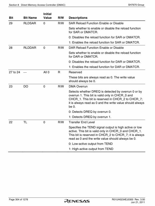
Section 8 Direct Memory Access Controller (DMAC)
Page 304 of 1278 R01UH0234EJ0300 Rev. 3.00 Jun 21, 2011
SH7670 Group
Bit Bit Name Initial Value R/W Descriptions
29 RLDSAR 0 R/W SAR Reload Function Enable or Disable
Sets whether to enable or disable the reload function for SAR or DMATCR.
0: Disables the reload function for SAR or DMATCR.
1: Enables the reload function for SAR or DMATCR.
28 RLDDAR 0 R/W DAR Reload Function Enable or Disable
Sets whether to enable or disable the reload function for DAR or DMATCR.
0: Disables the reload function for DAR or DMATCR.
1: Enables the reload function for DAR or DMATCR.
27 to 24 ⎯ All 0 R Reserved
These bits are always read as 0. The write value should always be 0.
23 DO 0 R/W DMA Overrun
Selects whether DREQ is detected by overrun 0 or by overrun 1. This bit is valid only in CHCR_0 and CHCR_1. This bit is reserved in CHCR_2 to CHCR_7; it is always read as 0 and the write value should always be 0.
0: Detects DREQ by overrun 0.
1: Detects DREQ by overrun 1.
22 TL 0 R/W Transfer End Level
Specifies the TEND signal output is high active or low active. This bit is valid only in CHCR_0 and CHCR_1. This bit is reserved in CHCR_2 to CHCR_7; it is always read as 0 and the write value should always be 0.
0: Low-active output from TEND
1: High-active output from TEND

Section 8 Direct Memory Access Controller (DMAC)
R01UH0234EJ0300 Rev. 3.00 Page 305 of 1278 Jun 21, 2011
SH7670 Group
Bit Bit Name Initial Value R/W Descriptions
21 ⎯ 0 R Reserved
These bits are always read as 0. The write value should always be 0.
20 TEMASK 0 R/W TE Set Mask
Indicates that DMA transfer is not terminated when the TE bit is set to 1. By setting this bit together with the SAR reload function or the DAR reload function, DMA transfer can be executed until the transfer request is canceled. Upon detection of the rising or falling edge of an auto request or external request, this bit is ignored and the DMA transfer is terminated when the TE bit is set. Note that this function is enabled if either of the RLDSAR bit or the RLDDAR bit is set to 1.
0: Terminates DMA if the TE bit is set.
1: Continues DMA even if the TE bit is set.
19 HE 0 R/(W)* Half-End Flag
This bit is set to 1 when the transfer count reaches half of the DMATCR value that was specified before transfer starts.
If DMA transfer ends because of an NMI interrupt, a DMA address error, or clearing of the DE bit or the DME bit in DMAOR before the transfer count reaches half of the initial DMATCR value, the HE bit is not set to 1. If DMA transfer ends due to an NMI interrupt, a DMA address error, or clearing of the DE bit or the DME bit in DMAOR after the HE bit is set to 1, the bit remains set to 1.
To clear the HE bit, write 0 to it after HE = 1 is read.
0: DMATCR > (DMATCR set before transfer starts)/2 during DMA transfer or after DMA transfer is terminated
[Clearing condition]
• Writing 0 after reading HE = 1.
1: DMATCR ≤ (DMATCR set before transfer starts)/2
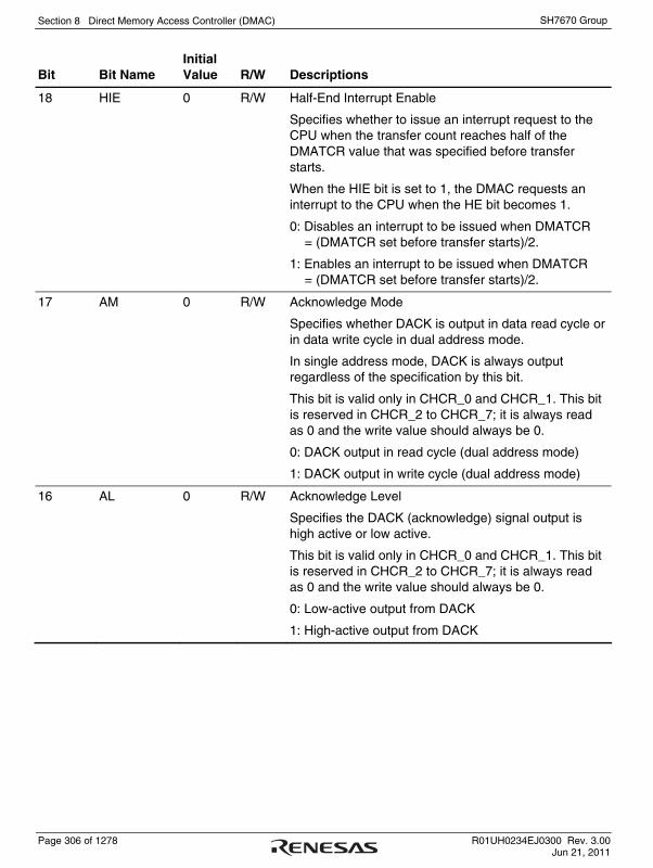
Section 8 Direct Memory Access Controller (DMAC)
Page 306 of 1278 R01UH0234EJ0300 Rev. 3.00 Jun 21, 2011
SH7670 Group
Bit Bit Name Initial Value R/W Descriptions
18 HIE 0 R/W Half-End Interrupt Enable
Specifies whether to issue an interrupt request to the CPU when the transfer count reaches half of the DMATCR value that was specified before transfer starts.
When the HIE bit is set to 1, the DMAC requests an interrupt to the CPU when the HE bit becomes 1.
0: Disables an interrupt to be issued when DMATCR = (DMATCR set before transfer starts)/2.
1: Enables an interrupt to be issued when DMATCR = (DMATCR set before transfer starts)/2.
17 AM 0 R/W Acknowledge Mode
Specifies whether DACK is output in data read cycle or in data write cycle in dual address mode.
In single address mode, DACK is always output regardless of the specification by this bit.
This bit is valid only in CHCR_0 and CHCR_1. This bit is reserved in CHCR_2 to CHCR_7; it is always read as 0 and the write value should always be 0.
0: DACK output in read cycle (dual address mode)
1: DACK output in write cycle (dual address mode)
16 AL 0 R/W Acknowledge Level
Specifies the DACK (acknowledge) signal output is high active or low active.
This bit is valid only in CHCR_0 and CHCR_1. This bit is reserved in CHCR_2 to CHCR_7; it is always read as 0 and the write value should always be 0.
0: Low-active output from DACK
1: High-active output from DACK

Section 8 Direct Memory Access Controller (DMAC)
R01UH0234EJ0300 Rev. 3.00 Page 307 of 1278 Jun 21, 2011
SH7670 Group
Bit Bit Name Initial Value R/W Descriptions
15, 14 DM[1:0] 00 R/W Destination Address Mode
These bits select whether the DMA destination address is incremented, decremented, or left fixed. (In single address mode, DM1 and DM0 bits are ignored when data is transferred to an external device with DACK.)
00: Fixed destination address
01: Destination address is incremented (+1 in 8-bit transfer, +2 in 16-bit transfer, +4 in 32-bit transfer, +16 in 16-byte transfer)
10: Destination address is decremented (–1 in 8-bit transfer, –2 in 16-bit transfer, –4 in 32-bit transfer, setting prohibited in 16-byte transfer)
11: Setting prohibited
13, 12 SM[1:0] 00 R/W Source Address Mode
These bits select whether the DMA source address is incremented, decremented, or left fixed. (In single address mode, SM1 and SM0 bits are ignored when data is transferred from an external device with DACK.)00: Fixed source address
01: Source address is incremented (+1 in byte-unit transfer, +2 in word-unit transfer, +4 in longword-unit transfer, +16 in 16-byte-unit transfer)
10: Source address is decremented (–1 in byte-unit transfer, –2 in word-unit transfer, –4 in longword-unit transfer, setting prohibited in 16-byte-unit transfer)
11: Setting prohibited
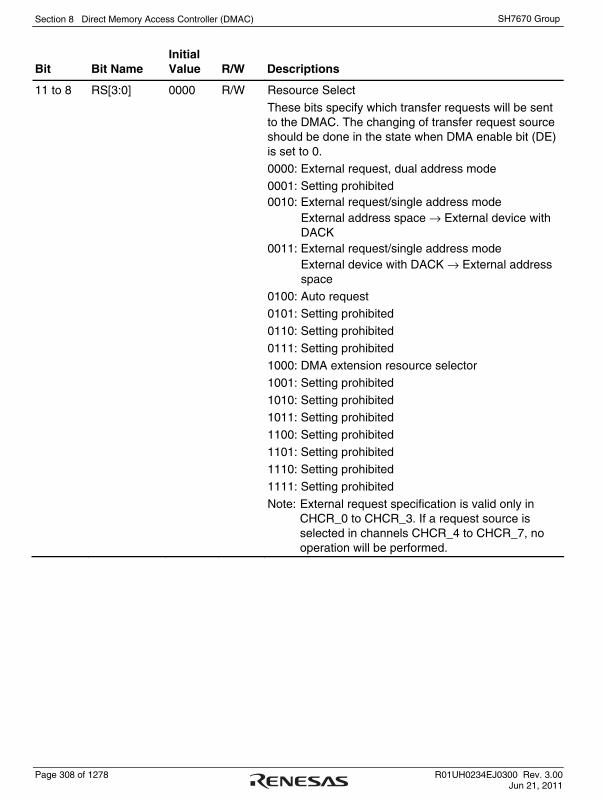
Section 8 Direct Memory Access Controller (DMAC)
Page 308 of 1278 R01UH0234EJ0300 Rev. 3.00 Jun 21, 2011
SH7670 Group
Bit Bit Name Initial Value R/W Descriptions
11 to 8 RS[3:0] 0000 R/W Resource Select
These bits specify which transfer requests will be sent to the DMAC. The changing of transfer request source should be done in the state when DMA enable bit (DE) is set to 0. 0000: External request, dual address mode 0001: Setting prohibited 0010: External request/single address mode
External address space → External device with DACK
0011: External request/single address mode External device with DACK → External address space
0100: Auto request 0101: Setting prohibited
0110: Setting prohibited
0111: Setting prohibited 1000: DMA extension resource selector
1001: Setting prohibited
1010: Setting prohibited 1011: Setting prohibited
1100: Setting prohibited
1101: Setting prohibited 1110: Setting prohibited
1111: Setting prohibited
Note: External request specification is valid only in CHCR_0 to CHCR_3. If a request source is selected in channels CHCR_4 to CHCR_7, no operation will be performed.
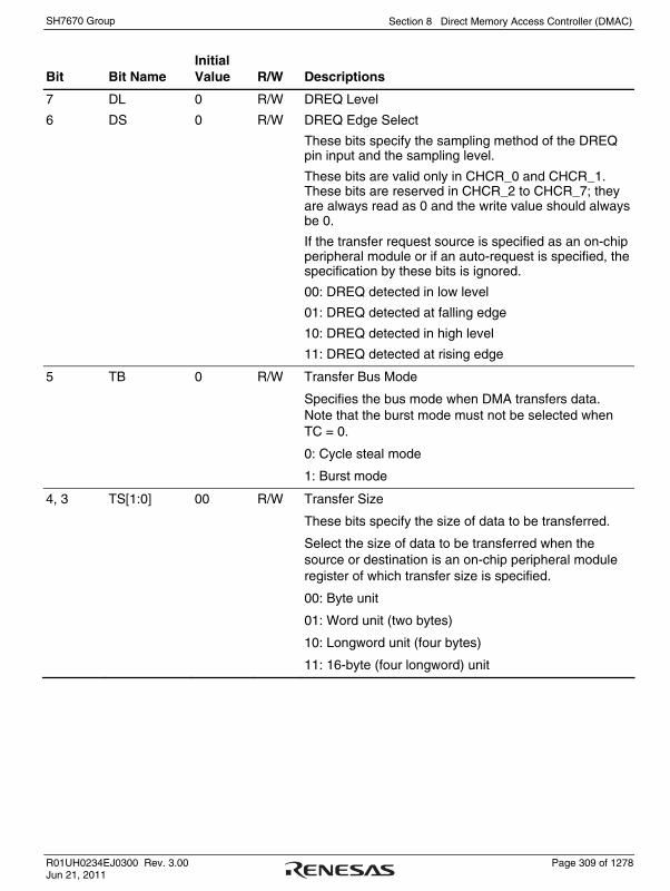
Section 8 Direct Memory Access Controller (DMAC)
R01UH0234EJ0300 Rev. 3.00 Page 309 of 1278 Jun 21, 2011
SH7670 Group
Bit Bit Name Initial Value R/W Descriptions
7
6
DL
DS
0
0
R/W
R/W
DREQ Level
DREQ Edge Select
These bits specify the sampling method of the DREQ pin input and the sampling level.
These bits are valid only in CHCR_0 and CHCR_1. These bits are reserved in CHCR_2 to CHCR_7; they are always read as 0 and the write value should always be 0.
If the transfer request source is specified as an on-chip peripheral module or if an auto-request is specified, the specification by these bits is ignored.
00: DREQ detected in low level
01: DREQ detected at falling edge
10: DREQ detected in high level
11: DREQ detected at rising edge
5 TB 0 R/W Transfer Bus Mode
Specifies the bus mode when DMA transfers data. Note that the burst mode must not be selected when TC = 0.
0: Cycle steal mode
1: Burst mode
4, 3 TS[1:0] 00 R/W Transfer Size
These bits specify the size of data to be transferred.
Select the size of data to be transferred when the source or destination is an on-chip peripheral module register of which transfer size is specified.
00: Byte unit
01: Word unit (two bytes)
10: Longword unit (four bytes)
11: 16-byte (four longword) unit
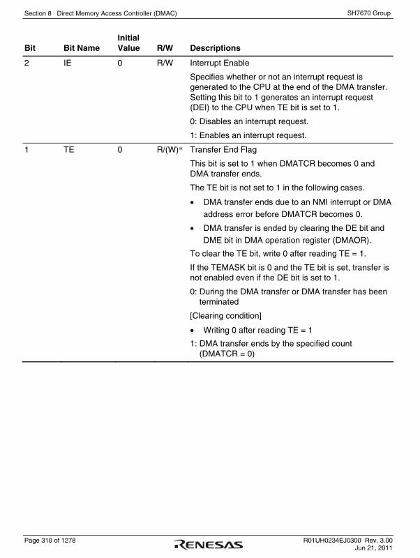
Section 8 Direct Memory Access Controller (DMAC)
Page 310 of 1278 R01UH0234EJ0300 Rev. 3.00 Jun 21, 2011
SH7670 Group
Bit Bit Name Initial Value R/W Descriptions
2 IE 0 R/W Interrupt Enable
Specifies whether or not an interrupt request is generated to the CPU at the end of the DMA transfer. Setting this bit to 1 generates an interrupt request (DEI) to the CPU when TE bit is set to 1.
0: Disables an interrupt request.
1: Enables an interrupt request.
1 TE 0 R/(W)* Transfer End Flag
This bit is set to 1 when DMATCR becomes 0 and DMA transfer ends.
The TE bit is not set to 1 in the following cases.
• DMA transfer ends due to an NMI interrupt or DMA
address error before DMATCR becomes 0.
• DMA transfer is ended by clearing the DE bit and
DME bit in DMA operation register (DMAOR).
To clear the TE bit, write 0 after reading TE = 1.
If the TEMASK bit is 0 and the TE bit is set, transfer is not enabled even if the DE bit is set to 1.
0: During the DMA transfer or DMA transfer has been terminated
[Clearing condition]
• Writing 0 after reading TE = 1
1: DMA transfer ends by the specified count (DMATCR = 0)

Section 8 Direct Memory Access Controller (DMAC)
R01UH0234EJ0300 Rev. 3.00 Page 311 of 1278 Jun 21, 2011
SH7670 Group
Bit Bit Name Initial Value R/W Descriptions
0 DE 0 R/W DMA Enable
Enables or disables the DMA transfer. In auto request mode, DMA transfer starts by setting the DE bit and DME bit in DMAOR to 1. In this case, all of the bits TE, NMIF in DMAOR, and AE must be 0. In an external request or peripheral module request, DMA transfer starts if DMA transfer request is generated by the devices or peripheral modules after setting the bits DE and DME to 1. If the TEMASK bit is 1, the NMIF and AE bits must be 0 upon detection of the low or high level of an external request and at a request of the peripheral module. If the TEMASK bit is 0, the TE bit must also be 0. As with auto request mode, all of the TE, NMIF, and AE bits must be 0 upon detection of the rising or falling edge of an external request. Clearing the DE bit to 0 can terminate the DMA transfer.
0: DMA transfer disabled
1: DMA transfer enabled
Note: * Only 0 can be written to clear the flag after 1 is read.
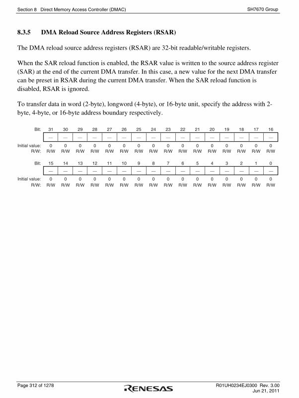
Section 8 Direct Memory Access Controller (DMAC)
Page 312 of 1278 R01UH0234EJ0300 Rev. 3.00 Jun 21, 2011
SH7670 Group
8.3.5 DMA Reload Source Address Registers (RSAR)
The DMA reload source address registers (RSAR) are 32-bit readable/writable registers.
When the SAR reload function is enabled, the RSAR value is written to the source address register (SAR) at the end of the current DMA transfer. In this case, a new value for the next DMA transfer can be preset in RSAR during the current DMA transfer. When the SAR reload function is disabled, RSAR is ignored.
To transfer data in word (2-byte), longword (4-byte), or 16-byte unit, specify the address with 2-byte, 4-byte, or 16-byte address boundary respectively.
31 30 29 28 27 26 25 24 23 22 21 20 19 18 17 16
15 14 13 12 11 10 9 8 7 6 5 4 3 2 1 0
0 0 0 0 0 0 0 0 0 0 0 0 0 0 0 0R/W R/W R/W R/W R/W R/W R/W R/W R/W R/W R/W R/W R/W R/W R/W R/W
0 0 0 0 0 0 0 0 0 0 0 0 0 0 0 0R/W R/W R/W R/W R/W R/W R/W R/W R/W R/W R/W R/W R/W R/W R/W R/W
Bit:
Initial value:R/W:
Bit:
Initial value:R/W:
⎯ ⎯ ⎯ ⎯ ⎯ ⎯ ⎯ ⎯ ⎯ ⎯ ⎯ ⎯ ⎯ ⎯ ⎯ ⎯
⎯ ⎯ ⎯ ⎯ ⎯ ⎯ ⎯ ⎯ ⎯ ⎯ ⎯ ⎯ ⎯ ⎯ ⎯ ⎯

Section 8 Direct Memory Access Controller (DMAC)
R01UH0234EJ0300 Rev. 3.00 Page 313 of 1278 Jun 21, 2011
SH7670 Group
8.3.6 DMA Reload Destination Address Registers (RDAR)
The DMA reload destination address registers (RDAR) are 32-bit readable/writable registers.
When the DAR reload function is enabled, the RDAR value is written to the destination address register (SAR) at the end of the current DMA transfer. In this case, a new value for the next DMA transfer can be preset in RDAR during the current DMA transfer. When the DAR reload function is disabled, RDAR is ignored.
To transfer data in word (2-byte), longword (4-byte), or 16-byte unit, specify the address with 2-byte, 4-byte, or 16-byte address boundary respectively.
31 30 29 28 27 26 25 24 23 22 21 20 19 18 17 16
15 14 13 12 11 10 9 8 7 6 5 4 3 2 1 0
0 0 0 0 0 0 0 0 0 0 0 0 0 0 0 0R/W R/W R/W R/W R/W R/W R/W R/W R/W R/W R/W R/W R/W R/W R/W R/W
0 0 0 0 0 0 0 0 0 0 0 0 0 0 0 0R/W R/W R/W R/W R/W R/W R/W R/W R/W R/W R/W R/W R/W R/W R/W R/W
Bit:
Initial value:R/W:
Bit:
Initial value:R/W:
⎯ ⎯ ⎯ ⎯ ⎯ ⎯ ⎯ ⎯ ⎯ ⎯ ⎯ ⎯ ⎯ ⎯ ⎯ ⎯
⎯ ⎯ ⎯ ⎯ ⎯ ⎯ ⎯ ⎯ ⎯ ⎯ ⎯ ⎯ ⎯ ⎯ ⎯ ⎯

Section 8 Direct Memory Access Controller (DMAC)
Page 314 of 1278 R01UH0234EJ0300 Rev. 3.00 Jun 21, 2011
SH7670 Group
8.3.7 DMA Reload Transfer Count Registers (RDMATCR)
The DMA reload transfer count registers (RDMATCR) are 32-bit readable/writable registers.
When the SAR or DAR reload function is enabled, the RDMATCR value is written to the transfer count register (DMATCR) at the end of the current DMA transfer. In this case, a new value for the next DMA transfer can be preset in RDMATCR during the current DMA transfer. When the SAR or DAR reload function is disabled, RDMATCR is ignored.
The upper eight bits of RDMATCR are always read as 0, and the write value should always be 0.
As in DMATCR, the transfer count is 1 when the setting is H'00000001, 16,777,215 when H'00FFFFFF is set, and 16,777,216 (the maximum) when H'00000000 is set. To transfer data in 16 bytes, one 16-byte transfer (128 bits) counts one.
0 0 0 0 0 0 0 0 0 0 0 0 0 0 0 0R R R R R R R R R/W R/W R/W R/W R/W R/W R/W R/W
0 0 0 0 0 0 0 0 0 0 0 0 0 0 0 0R/W R/W R/W R/W R/W R/W R/W R/W R/W R/W R/W R/W R/W R/W R/W R/W
Bit:
Initial value:R/W:
Bit:
Initial value:R/W:
31 30 29 28 27 26 25 24 23 22 21 20 19 18 17 16
15 14 13 12 11 10 9 8 7 6 5 4 3 2 1 0
⎯ ⎯ ⎯ ⎯ ⎯ ⎯ ⎯ ⎯ ⎯ ⎯ ⎯ ⎯ ⎯ ⎯ ⎯ ⎯
⎯ ⎯ ⎯ ⎯ ⎯ ⎯ ⎯ ⎯ ⎯ ⎯ ⎯ ⎯ ⎯ ⎯ ⎯ ⎯
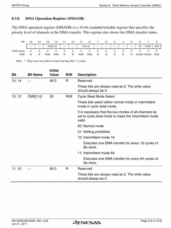
Section 8 Direct Memory Access Controller (DMAC)
R01UH0234EJ0300 Rev. 3.00 Page 315 of 1278 Jun 21, 2011
SH7670 Group
8.3.8 DMA Operation Register (DMAOR)
The DMA operation register (DMAOR) is a 16-bit readable/writable register that specifies the priority level of channels at the DMA transfer. This register also shows the DMA transfer status.
15 14 13 12 11 10 9 8 7 6 5 4 3 2 1 0
0 0 0 0 0 0 0 0 0 0 0 0 0 0 0 0R R R/W R/W R R R/W R/W R R R R R R/(W)* R/(W)* R/W
Note: Only 0 can be written to clear the flag after 1 is read.*
Bit:
Initial value:R/W:
⎯ ⎯ CMS[1:0] ⎯ ⎯ PR[1:0] ⎯ ⎯ ⎯ ⎯ ⎯ AE NMIF DME
Bit Bit Name Initial Value R/W Description
15, 14 ⎯ All 0 R Reserved
These bits are always read as 0. The write value should always be 0.
13, 12 CMS[1:0] 00 R/W Cycle Steal Mode Select
These bits select either normal mode or intermittent mode in cycle steal mode.
It is necessary that the bus modes of all channels be set to cycle steal mode to make the intermittent mode valid.
00: Normal mode
01: Setting prohibited
10: Intermittent mode 16
Executes one DMA transfer for every 16 cycles of Bφ clock.
11: Intermittent mode 64
Executes one DMA transfer for every 64 cycles of Bφ clock.
11, 10 ⎯ All 0 R Reserved
These bits are always read as 0. The write value should always be 0.
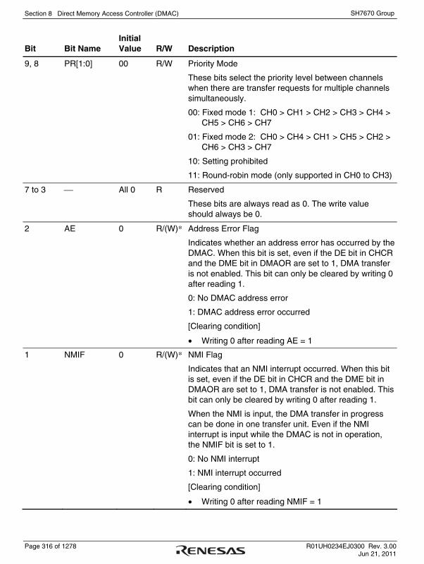
Section 8 Direct Memory Access Controller (DMAC)
Page 316 of 1278 R01UH0234EJ0300 Rev. 3.00 Jun 21, 2011
SH7670 Group
Bit Bit Name Initial Value R/W Description
9, 8 PR[1:0] 00 R/W Priority Mode
These bits select the priority level between channels when there are transfer requests for multiple channels simultaneously.
00: Fixed mode 1: CH0 > CH1 > CH2 > CH3 > CH4 > CH5 > CH6 > CH7
01: Fixed mode 2: CH0 > CH4 > CH1 > CH5 > CH2 > CH6 > CH3 > CH7
10: Setting prohibited
11: Round-robin mode (only supported in CH0 to CH3)
7 to 3 ⎯ All 0 R Reserved
These bits are always read as 0. The write value should always be 0.
2 AE 0 R/(W)* Address Error Flag
Indicates whether an address error has occurred by the DMAC. When this bit is set, even if the DE bit in CHCR and the DME bit in DMAOR are set to 1, DMA transfer is not enabled. This bit can only be cleared by writing 0 after reading 1.
0: No DMAC address error
1: DMAC address error occurred
[Clearing condition]
• Writing 0 after reading AE = 1
1 NMIF 0 R/(W)* NMI Flag
Indicates that an NMI interrupt occurred. When this bit is set, even if the DE bit in CHCR and the DME bit in DMAOR are set to 1, DMA transfer is not enabled. This bit can only be cleared by writing 0 after reading 1.
When the NMI is input, the DMA transfer in progress can be done in one transfer unit. Even if the NMI interrupt is input while the DMAC is not in operation, the NMIF bit is set to 1.
0: No NMI interrupt
1: NMI interrupt occurred
[Clearing condition]
• Writing 0 after reading NMIF = 1

Section 8 Direct Memory Access Controller (DMAC)
R01UH0234EJ0300 Rev. 3.00 Page 317 of 1278 Jun 21, 2011
SH7670 Group
Bit Bit Name Initial Value R/W Description
0 DME 0 R/W DMA Master Enable
Enables or disables DMA transfer on all channels. If the DME bit and DE bit in CHCR are set to 1, DMA transfer is enabled.
However, transfer is enabled only when the TE bit in CHCR of the transfer corresponding channel, the NMIF bit in DMAOR, and the AE bit are all cleared to 0. Clearing the DME bit to 0 can terminate the DMA transfer on all channels.
0: DMA transfer is disabled on all channels
1: DMA transfer is enabled on all channels
Note: * Only 0 can be written to clear the flag after 1 is read.
If the priority mode bits are modified after a DMA transfer, the channel priority is initialized. If fixed mode 2 is specified, the channel priority is specified as CH0 > CH4 > CH1 > CH5 > CH2 > CH6 > CH3 > CH7. If fixed mode 1 is specified, the channel priority is specified as CH0 > CH1 > CH2 > CH3 > CH4 > CH5 > CH6 > CH7. If the round-robin mode is specified, the transfer end channel is reset.
Table 8.3 shows the priority change in each mode (modes 0 to 2) specified by the priority mode bits. In each priority mode, the channel priority to accept the next transfer request may change in up to three ways according to the transfer end channel.
For example, when the transfer end channel is channel 1, the priority of the channel to accept the next transfer request is specified as CH2 > CH3 > CH0 >CH1 > CH4 > CH5 > CH6 > CH7. When the transfer end channel is any one of the channels 4 to 7, round-robin will not be applied and the priority level is not changed at the end of transfer in the channels 4 to 7.
The DMAC internal operation for an address error is as follows:
• No address error: Read (source to DMAC) → Write (DMAC to destination)
• Address error in source address: Nop → Nop
• Address error in destination address: Read → Nop

Section 8 Direct Memory Access Controller (DMAC)
Page 318 of 1278 R01UH0234EJ0300 Rev. 3.00 Jun 21, 2011
SH7670 Group
Table 8.3 Combinations of Priority Mode Bits
Priority Level at the End of Transfer Transfer
End
Priority Mode
Bits High Low
Mode CH No. PR[1] PR[0] 0 1 2 3 4 5 6 7
Mode 0
(fixed mode 1)
Any channel 0 0 CH0 CH1 CH2 CH3 CH4 CH5 CH6 CH7
Mode 1
(fixed mode 2)
Any channel 0 1 CH0 CH4 CH1 CH5 CH2 CH6 CH3 CH7
CH0 1 1 CH1 CH2 CH3 CH0 CH4 CH5 CH6 CH7
CH1 1 1 CH2 CH3 CH0 CH1 CH4 CH5 CH6 CH7
CH2 1 1 CH3 CH0 CH1 CH2 CH4 CH5 CH6 CH7
CH3 1 1 CH0 CH1 CH2 CH3 CH4 CH5 CH6 CH7
CH4 1 1 CH0 CH1 CH2 CH3 CH4 CH5 CH6 CH7
CH5 1 1 CH0 CH1 CH2 CH3 CH4 CH5 CH6 CH7
CH6 1 1 CH0 CH1 CH2 CH3 CH4 CH5 CH6 CH7
Mode 2
(round-robin mode)
CH7 1 1 CH0 CH1 CH2 CH3 CH4 CH5 CH6 CH7

Section 8 Direct Memory Access Controller (DMAC)
R01UH0234EJ0300 Rev. 3.00 Page 319 of 1278 Jun 21, 2011
SH7670 Group
8.3.9 DMA Extension Resource Selectors 0 to 3 (DMARS0 to DMARS3)
The DMA extension resource selectors (DMARS) are 16-bit readable/writable registers that specify the DMA transfer sources from peripheral modules in each channel. DMARS0 is for channels 0 and 1, DMARS1 is for channels 2 and 3, DMARS2 is for channels 4 and 5, and DMARS3 is for channels 6 and 7. Table 8.4 shows the specifiable combinations.
This register can specify transfer requests from six SCIF sources, two IIC3 sources, two CMT sources, two USB sources, two SSI sources, and two SDHI sources.
• DMARS0
15 14 13 12 11 10 9 8 7 6 5 4 3 2 1 0
0 0 0 0 0 0 0 0 0 0 0 0 0 0 0 0R/W R/W R/W R/W R/W R/W R/W R/W R/W R/W R/W R/W R/W R/W R/W R/W
Bit:
Initial value:R/W:
CH1 MID[5:0] CH1 RID[1:0] CH0 RID[1:0]CH0 MID[5:0]
• DMARS1
15 14 13 12 11 10 9 8 7 6 5 4 3 2 1 0
0 0 0 0 0 0 0 0 0 0 0 0 0 0 0 0R/W R/W R/W R/W R/W R/W R/W R/W R/W R/W R/W R/W R/W R/W R/W R/W
Bit:
Initial value:R/W:
CH3 MID[5:0] CH3 RID[1:0] CH2 RID[1:0]CH2 MID[5:0]
• DMARS2
15 14 13 12 11 10 9 8 7 6 5 4 3 2 1 0
0 0 0 0 0 0 0 0 0 0 0 0 0 0 0 0R/W R/W R/W R/W R/W R/W R/W R/W R/W R/W R/W R/W R/W R/W R/W R/W
Bit:
Initial value:R/W:
CH5 MID[5:0] CH5 RID[1:0] CH4 RID[1:0]CH4 MID[5:0]
• DMARS3
15 14 13 12 11 10 9 8 7 6 5 4 3 2 1 0
0 0 0 0 0 0 0 0 0 0 0 0 0 0 0 0R/W R/W R/W R/W R/W R/W R/W R/W R/W R/W R/W R/W R/W R/W R/W R/W
Bit:
Initial value:R/W:
CH7 MID[5:0] CH7 RID[1:0] CH6 RID[1:0]CH6 MID[5:0]
Transfer requests from the various modules specify MID and RID as shown in table 8.4.

Section 8 Direct Memory Access Controller (DMAC)
Page 320 of 1278 R01UH0234EJ0300 Rev. 3.00 Jun 21, 2011
SH7670 Group
Table 8.4 DMARS Settings
Peripheral Module
Setting Value for One Channel ({MID, RID})
MID
RID
Function
USB_0 H'03 B'000000 B'11 ⎯
USB_1 H'07 B'000001 B'11 ⎯
H'11 B'000100 B'01 Transmit SDHI
H'12 B'000100 B'10 Receive
SSI_0 H'23 B'001000 B'11 ⎯
SSI_1 H'27 B'001001 B'11 ⎯
H'61 B'01 Transmit IIC3_0
H'62
B'011000
B'10 Receive
H'81 B'01 Transmit SCIF_0
H'82
B'100000
B'10 Receive
H'85 B'01 Transmit SCIF_1
H'86
B'100001
B'10 Receive
H'89 B'01 Transmit SCIF_2
H'8A
B'100010
B'10 Receive
CMT_0 H'FB B'111110 B'11 ⎯
CMT_1 H'FF B'111111 B'11 ⎯
When MID or RID other than the values listed in table 8.4 is set, the operation of this LSI is not guaranteed. The transfer request from DMARS is valid only when the resource select bits (RS[3:0]) in CHCR0 to CHCR7 have been set to B'1000. Otherwise, even if DMARS has been set, the transfer request source is not accepted.

Section 8 Direct Memory Access Controller (DMAC)
R01UH0234EJ0300 Rev. 3.00 Page 321 of 1278 Jun 21, 2011
SH7670 Group
8.4 Operation
When there is a DMA transfer request, the DMAC starts the transfer according to the predetermined channel priority order; when the transfer end conditions are satisfied, it ends the transfer. Transfers can be requested in three modes: auto request, external request, and on-chip peripheral module request. In bus mode, the burst mode or the cycle steal mode can be selected.
8.4.1 Transfer Flow
After the DMA source address registers (SAR), DMA destination address registers (DAR), DMA transfer count registers (DMATCR), DMA channel control registers (CHCR), DMA operation register (DMAOR), three reload registers (RSAR, RDAR, and RDMATCR), and DMA extension resource selector (DMARS) are set for the target transfer conditions, the DMAC transfers data according to the following procedure:
1. Checks to see if transfer is enabled (DE = 1, DME = 1, TEMASK = 0 and TE = 0 [or TEMASK = 1], AE = 0, NMIF = 0)
2. When a transfer request comes and transfer is enabled, the DMAC transfers one transfer unit of data (depending on the TS[1:0] settings). For an auto request, the transfer begins automatically when the DE bit and DME bit are set to 1. The DMATCR value will be decremented by 1 for each transfer. The actual transfer flows vary by address mode and bus mode.
3. When half of the specified transfer count is exceeded (when DMATCR reaches half of the initial value), an HEI interrupt is sent to the CPU if the HIE bit in CHCR is set to 1.
4. When TEMASK = 0, if transfer has been completed for the specified count (that is, DMATCR reaches 0), the transfer ends normally. If the IE bit in CHCR is set to 1 at this time, a DEI interrupt is sent to the CPU. When TEMASK = 1, if DMATCR reaches 0, TE is set to 1. The specified RSAR, RDAR, and RDMATC values are reloaded into RSAR, RDAR, and RDMATC, and the transfer operation continues until there are no more transfer requests.
5. When an address error in the DMAC or an NMI interrupt is generated, the transfer is terminated. Transfers are also terminated when the DE bit in CHCR or the DME bit in DMAOR is cleared to 0.
Figure 8.2 is a flowchart of this procedure.

Section 8 Direct Memory Access Controller (DMAC)
Page 322 of 1278 R01UH0234EJ0300 Rev. 3.00 Jun 21, 2011
SH7670 Group
Start
Initial settings (SAR, DAR, DMATCR, CHCR,
DMAOR, DMARS)
DE, DME = 1 andNMIF, AE, TE = 0?
No
No
Yes
Yes
Transfer requestoccurs?*1
Transfer (one transfer unit);DMATCR – 1 → DMATCR,
SAR and DAR updated
DMATCR = 0?No
NoYes
Yes
No
No
No
DEI interrupt request(when IE = 1)
For a request from anon-chip peripheral module,
the transfer acknowledge signalis sent to the module.
When reload function is enabled,RSAR → SAR, RDAR → DAR,and RDMATCR → DMATCR
TE = 1
NMIF = 1or AE = 1 or DE = 0
or DME = 0?
NMIF = 1or AE = 1 or DE = 0
or DME = 0?
Transfer end Transfer terminatedNormal end
Bus mode,transfer request mode,
DREQ detection system*3
*2
Yes YesYes
DMATCR=1/2 ?
HEI interrupt request(when HE = 1)
HE=1
When the TC bit in CHCR is 0, or for a request from an on-chip peripheral
module, the transfer acknowledgesignal is sent to the module.
Notes: 1. In auto-request mode, transfer begins when the NMIF, AE, and TE bits are cleared to 0 and the DE and DME bits are set to 1.
2. DREQ level detection in burst mode (external request) or cycle steal mode. 3. DREQ edge detection in burst mode (external request), or auto request mode in burst mode.
Upon detection of the level of an external
request or at a request of an on-chip peripheral module, is the
TEMASK bit set to 1?
Figure 8.2 DMA Transfer Flowchart

Section 8 Direct Memory Access Controller (DMAC)
R01UH0234EJ0300 Rev. 3.00 Page 323 of 1278 Jun 21, 2011
SH7670 Group
8.4.2 DMA Transfer Requests
DMA transfer requests are basically generated in either the data transfer source or destination, but they can also be generated in external devices and on-chip peripheral modules that are neither the transfer source nor destination.
Transfers can be requested in three modes: auto request, external request, and on-chip peripheral module request. The request mode is selected by the RS[3:0] bits in CHCR_0 to CHCR_7 and DMARS0 to DMARS3.
(1) Auto-Request Mode
When there is no transfer request signal from an external source, as in a memory-to-memory transfer or a transfer between memory and an on-chip peripheral module unable to request a transfer, the auto-request mode allows the DMAC to automatically generate a transfer request signal internally. When the DE bits in CHCR_0 to CHCR_7 and the DME bit in DMAOR are set to 1, the transfer begins so long as the TE bits in CHCR_0 to CHCR_7, and the AE and NMIF bits in DMAOR are 0.
(2) External Request Mode
In this mode a transfer is performed at the request signals (DREQ0 and DREQ1) of an external device. Choose one of the modes shown in table 8.5 according to the application system. When the DMA transfer is enabled (for level detection, DE=1, DME=1, TEMASK = 0 and TE = 0 [or TEMASK = 1], AE=0, NMIF=0); for edge detection, DE=1, DME=1, TE=0, AE=0, NMIF=0), DMA transfer is performed upon a request at the DREQ input.
Table 8.5 Selecting External Request Modes with the RS Bits
RS[3]
RS[2]
RS[1]
RS[0]
Address Mode
Transfer Source
Transfer Destination
0 0 0 0 Dual address mode Any Any
0 External memory, memory-mapped external device
External device with DACK
0 0 1
1
Single address mode
External device with DACK
External memory, memory-mapped external device

Section 8 Direct Memory Access Controller (DMAC)
Page 324 of 1278 R01UH0234EJ0300 Rev. 3.00 Jun 21, 2011
SH7670 Group
Choose to detect DREQ by either the edge or level of the signal input with the DL and DS bits in CHCR_0 and CHCR_1 as shown in table 8.6. The source of the transfer request does not have to be the data transfer source or destination. Upon detection of a rising or falling edge, one transfer request in burst mode causes the transfer to continue until DMATCR = 0 is reached. In cycle steal mode, one transfer request results in a single transfer.
Table 8.6 Selecting External Request Detection with DL and DS Bits
CHCR
DL bit DS bit Detection of External Request
0 Low level detection 0
1 Falling edge detection
0 High level detection 1
1 Rising edge detection
When DREQ is accepted, the DREQ pin enters the request accept disabled state (non-sensitive period). After issuing acknowledge DACK signal for the accepted DREQ, the DREQ pin again enters the request accept enabled state.
When DREQ is used by level detection, there are following two cases by the timing to detect the next DREQ after outputting DACK.
Overrun 0: Transfer is terminated after the same number of transfer has been performed as requests.
Overrun 1: Transfer is terminated after transfers have been performed for (the number of requests plus 1) times.
The DO bit in CHCR selects this overrun 0 or overrun 1.
Table 8.7 Selecting External Request Detection with DO Bit
CHCR
DO bit External Request
0 Overrun 0
1 Overrun 1

Section 8 Direct Memory Access Controller (DMAC)
R01UH0234EJ0300 Rev. 3.00 Page 325 of 1278 Jun 21, 2011
SH7670 Group
(3) On-Chip Peripheral Module Request
In this mode, the transfer is performed in response to the DMA transfer request signal from an on-chip peripheral module.
Table 8.8 shows the list of DMAC transfer request signals sent from on-chip peripheral modules to DMAC.
When a transfer request signal is sent in on-chip peripheral module request mode while DMA transfer is enabled (DE=1, DME=1, TEMASK = 0 and TE = 0 [or TEMASK = 1], AE=0, NMIF=0), DMA transfer is performed.
For on-chip peripheral module requests, there are cases in which the transfer source and destination are fixed; see table 8.8.

Section 8 Direct Memory Access Controller (DMAC)
Page 326 of 1278 R01UH0234EJ0300 Rev. 3.00 Jun 21, 2011
SH7670 Group
Table 8.8 Selecting On-Chip Peripheral Module Request Modes with RS3 to RS0 Bits
CHCR DMARS
RS[3:0] MID RID
DMA Transfer Request Source
DMA Transfer Request Signal
Transfer Source
Transfer Destination Bus Mode
USB_DMA0 (receive FIFO full)
D0FIFO Any 000000 11 USB
USB_DMA0 (transmit FIFO empty)
Any D0FIFO
USB_DMA1 (receive FIFO full)
D1FIFO Any 000001 11 USB
USB_DMA1 (transmit FIFO empty)
Any D1FIFO
Cycle steal or burst
01 SDHI transmit TXI (receive data empty) Data register Any 000100
10 SDHI receive RXI (transmit data full) Any Data register
DMA0 (transmit mode) Any SSITDR0 001000 11 SSI_0
DMA0 (receive mode) SSIRDR0 Any
DMA1 (transmit mode) Any SSITDR1 001001 11 SSI_1
DMA1 (receive mode) SSIRDR1 Any
01 IIC3_0 transmit TXI0 (transmit data empty) Any ICDRT0 011000
10 IIC3_0 receive RXI0 (receive data full) ICDRR0 Any
01 SCIF_0 transmit TXI0 (transmit FIFO data empty)
Any SCFTDR_0 100000
10 SCIF_0 receive RXI0 (receive FIFO data full)
SCFRDR_0 Any
01 SCIF_1 transmit TXI1 (transmit FIFO data empty)
Any SCFTDR_1 100001
10 SCIF_1 receive RXI1 (receive FIFO data full)
SCFRDR_1 Any
01 SCIF_2 transmit TXI2 (transmit FIFO data empty)
Any SCFTDR_2 100010
10 SCIF_2 receive RXI2 (receive FIFO data full)
SCFRDR_2 Any
Cycle steal
111110 11 CMT_0 CMI0 (compare match) Any Any
1000
111111 11 CMT_1 CMI1 (compare match) Any Any
Cycle steal or burst

Section 8 Direct Memory Access Controller (DMAC)
R01UH0234EJ0300 Rev. 3.00 Page 327 of 1278 Jun 21, 2011
SH7670 Group
8.4.3 Channel Priority
When the DMAC receives simultaneous transfer requests on two or more channels, it selects a channel according to a predetermined priority order. Three modes (fixed mode 1, fixed mode 2, and round-robin mode) are selected using the PR1 and PR0 bits in DMAOR.
(1) Fixed Mode
In fixed modes, the priority levels among the channels remain fixed. There are two kinds of fixed modes as follows:
Fixed mode 1: CH0 > CH1 > CH2 > CH3 > CH4 > CH5 > CH6 > CH7
Fixed mode 2: CH0 > CH4 > CH1 > CH5 > CH2 > CH6 > CH3 > CH7
These are selected by the PR1 and PR0 bits in the DMA operation register (DMAOR).
(2) Round-Robin Mode
Each time one unit of word, byte, longword, or 16 bytes is transferred on one channel, the priority order is rotated. The channel on which the transfer was just finished is rotated to the lowest of the priority order among the four round-robin channels (channels 0 to 4). The priority of the channels other than the round-robin channels (channels 0 to 4) does not change even in round-robin mode. The round-robin mode operation is shown in figure 8.3. The priority in round-robin mode is CH0 > CH1 > CH2 > CH3 > CH4 > CH5 > CH6 > CH7 immediately after a reset.
When the round-robin mode has been specified, do not concurrently specify cycle steal mode and burst mode as the bus modes of any two or more channels.

Section 8 Direct Memory Access Controller (DMAC)
Page 328 of 1278 R01UH0234EJ0300 Rev. 3.00 Jun 21, 2011
SH7670 Group
Channel 2 is given the lowest priority among the round-robin channels. The priority of channels 0 and 1, which were higher than channel 2, is also shifted. If there is a transfer request only to channel 5 immediately after that, the priority does not change because channel 5 is not a round-robin channel.
Channel 1 is given the lowest priority among the round-robin channels. The priority of channel 0, which was higher than channel 1, is also shifted.
Channel 0 is given the lowest priority among the round-robin channels.
CH0 > CH1 > CH2 > CH3 > CH4 > CH5 > CH6 > CH7
CH1 > CH2 > CH3 > CH0 > CH4 > CH5 > CH6 > CH7
CH0 > CH1 > CH2 > CH3 > CH4 > CH5 > CH6 > CH7
CH2 > CH3 > CH0 > CH1 > CH4 > CH5 > CH6 > CH7
CH0 > CH1 > CH2 > CH3 > CH4 > CH5 > CH6 > CH7
CH3 > CH0 > CH1 > CH2 > CH4 > CH5 > CH6 > CH7
CH0 > CH1 > CH2 > CH3 > CH4 > CH5 > CH6 > CH7
CH0 > CH1 > CH2 > CH3 > CH4 > CH5 > CH6 > CH7
CH3 > CH0 > CH1 > CH2 > CH4 > CH5 > CH6 > CH7
(1) When channel 0 transfers
Initial priority order
Initial priority order
Initial priority order
Initial priority order
Priority orderafter transfer
Priority orderafter transfer
Priority orderafter transfer
Priority orderafter transfer
Post-transfer priority orderwhen there is an
immediate transfer request to channel 5 only
(2) When channel 1 transfers
(3) When channel 2 transfers
(4) When channel 7 transfers
Priority order does not change.
Figure 8.3 Round-Robin Mode

Section 8 Direct Memory Access Controller (DMAC)
R01UH0234EJ0300 Rev. 3.00 Page 329 of 1278 Jun 21, 2011
SH7670 Group
Figure 8.4 shows how the priority order changes when channel 0 and channel 3 transfers are requested simultaneously and a channel 1 transfer is requested during the channel 0 transfer. The DMAC operates as follows:
1. Transfer requests are generated simultaneously to channels 0 and 3.
2. Channel 0 has a higher priority, so the channel 0 transfer begins first (channel 3 waits for transfer).
3. A channel 1 transfer request occurs during the channel 0 transfer (channels 1 and 3 are both waiting)
4. When the channel 0 transfer ends, channel 0 is given the lowest priority among the round-robin channels.
5. At this point, channel 1 has a higher priority than channel 3, so the channel 1 transfer begins (channel 3 waits for transfer).
6. When the channel 1 transfer ends, channel 1 is given the lowest priority among the round-robin channels.
7. The channel 3 transfer begins.
8. When the channel 3 transfer ends, channels 3 and 2 are lowered in priority so that channel 3 is given the lowest priority among the round-robin channels.
Transfer request Waiting channel(s) DMAC operation Channel priority
(1) Channels 0 and 3
(3) Channel 1
0 > 1 > 2 > 3 > 4 > 5 > 6 > 7(2) Channel 0 transfer start
(4) Channel 0 transfer ends
(5) Channel 1 transfer starts
(6) Channel 1 transfer ends
(7) Channel 3 transfer starts
(8) Channel 3 transfer ends
1 > 2 > 3 > 0 > 4 > 5 > 6 > 7
2 > 3 > 0 > 1 > 4 > 5 > 6 > 7
0 > 1 > 2 > 3 > 4 > 5 > 6 > 7
Priority orderchanges
Priority orderchanges
Priority orderchanges
None
3
3
1, 3
Figure 8.4 Changes in Channel Priority in Round-Robin Mode
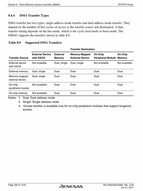
Section 8 Direct Memory Access Controller (DMAC)
Page 330 of 1278 R01UH0234EJ0300 Rev. 3.00 Jun 21, 2011
SH7670 Group
8.4.4 DMA Transfer Types
DMA transfer has two types; single address mode transfer and dual address mode transfer. They depend on the number of bus cycles of access to the transfer source and destination. A data transfer timing depends on the bus mode, which is the cycle steal mode or burst mode. The DMAC supports the transfers shown in table 8.9.
Table 8.9 Supported DMA Transfers
Transfer Destination
Transfer Source External Device with DACK
External Memory
Memory-Mapped External Device
On-Chip Peripheral Module
On-Chip Memory
External device with DACK
Not available Dual, single Dual, single Not available Not available
External memory Dual, single Dual Dual Dual Dual
Memory-mapped external device
Dual, single Dual Dual Dual Dual
On-chip peripheral module
Not available Dual Dual Dual Dual
On-chip memory Not available Dual Dual Dual Dual
Notes: 1. Dual: Dual address mode 2. Single: Single address mode
3. 16-byte transfer is available only for on-chip peripheral modules that support longword access.

Section 8 Direct Memory Access Controller (DMAC)
R01UH0234EJ0300 Rev. 3.00 Page 331 of 1278 Jun 21, 2011
SH7670 Group
(1) Address Modes
(a) Dual Address Mode
In dual address mode, both the transfer source and destination are accessed (selected) by an address. The transfer source and destination can be located externally or internally.
DMA transfer requires two bus cycles because data is read from the transfer source in a data read cycle and written to the transfer destination in a data write cycle. At this time, transfer data is temporarily stored in the DMAC. In the transfer between external memories as shown in figure 8.5, data is read to the DMAC from one external memory in a data read cycle, and then that data is written to the other external memory in a data write cycle.
Data buffer
Add
ress
bus
Dat
a bu
s
Add
ress
bus
Dat
a bu
sMemory
Transfer source module
Transfer destination module
Memory
Transfer source module
Transfer destination module
SAR
DAR
Data buffer
SAR
DAR
The SAR value is an address, data is read from the transfer source module,and the data is tempolarily stored in the DMAC.
First bus cycle
Second bus cycle
The DAR value is an address and the value stored in the data buffer in the DMAC is written to the transfer destination module.
DMAC
DMAC
Figure 8.5 Data Flow of Dual Address Mode
Auto request, external request, and on-chip peripheral module request are available for the transfer request. DACK can be output in read cycle or write cycle in dual address mode. The AM bit in the channel control register (CHCR) can specify whether the DACK is output in read cycle or write cycle.
Figure 8.6 shows an example of DMA transfer timing in dual address mode.

Section 8 Direct Memory Access Controller (DMAC)
Page 332 of 1278 R01UH0234EJ0300 Rev. 3.00 Jun 21, 2011
SH7670 Group
CKIO
A25 to A0
D31 to D0
DACKn(Active-low)
CSn
WEn
RD
Data read cycle Data write cycle
(1st cycle) (2nd cycle)
Transfer source address
Transfer destination address
Note: In transfer between external memories, with DACK output in the read cycle, DACK output timing is the same as that of CSn.
Figure 8.6 Example of DMA Transfer Timing in Dual Mode (Transfer Source: Normal Memory, Transfer Destination: Normal Memory)

Section 8 Direct Memory Access Controller (DMAC)
R01UH0234EJ0300 Rev. 3.00 Page 333 of 1278 Jun 21, 2011
SH7670 Group
(b) Single Address Mode
In single address mode, both the transfer source and destination are external devices, either of them is accessed (selected) by the DACK signal, and the other device is accessed by an address. In this mode, the DMAC performs one DMA transfer in one bus cycle, accessing one of the external devices by outputting the DACK transfer request acknowledge signal to it, and at the same time outputting an address to the other device involved in the transfer. For example, in the case of transfer between external memory and an external device with DACK shown in figure 8.7, when the external device outputs data to the data bus, that data is written to the external memory in the same bus cycle.
External address bus External data bus
DMAC Externalmemory
DACK
DREQ
Data flow (from memory to device)
Data flow (from device to memory)
External devicewith DACK
This LSI
Figure 8.7 Data Flow in Single Address Mode
Two kinds of transfer are possible in single address mode: (1) transfer between an external device with DACK and a memory-mapped external device, and (2) transfer between an external device with DACK and external memory. In both cases, only the external request signal (DREQ) is used for transfer requests.
Figure 8.8 shows an example of DMA transfer timing in single address mode.

Section 8 Direct Memory Access Controller (DMAC)
Page 334 of 1278 R01UH0234EJ0300 Rev. 3.00 Jun 21, 2011
SH7670 Group
Address output to external memory space
Select signal to external memory space
Select signal to external memory space
Data output from external device with DACK
DACK signal (active-low) to external device with DACK
Write strobe signal to external memory space
Address output to external memory space
Data output from external memory space
DACK signal (active-low) to external device with DACK
Read strobe signal to external memory space
(a) External device with DACK → External memory space (normal memory)
(b) External memory space (normal memory) → External device with DACK
CK
A25 to A0
D31 to D0
DACKn
CSn
WEn
CK
A25 to A0
D31 to D0
DACKn
CSn
RD
Figure 8.8 Example of DMA Transfer Timing in Single Address Mode
(2) Bus Modes
There are two bus modes; cycle steal and burst. Select the mode by the TB bits in the channel control registers (CHCR).
(a) Cycle Steal Mode
• Normal mode
In normal mode of cycle steal, the bus mastership is given to another bus master after a one-transfer-unit (byte, word, longword, or 16-byte unit) DMA transfer. When another transfer request occurs, the bus mastership is obtained from another bus master and a transfer is performed for one transfer unit. When that transfer ends, the bus mastership is passed to another bus master. This is repeated until the transfer end conditions are satisfied.
The cycle-steal normal mode can be used for any transfer section; transfer request source, transfer source, and transfer destination.
Figure 8.9 shows an example of DMA transfer timing in cycle-steal normal mode. Transfer conditions shown in the figure are;
⎯ Dual address mode
⎯ DREQ low level detection

Section 8 Direct Memory Access Controller (DMAC)
R01UH0234EJ0300 Rev. 3.00 Page 335 of 1278 Jun 21, 2011
SH7670 Group
CPU CPU CPU DMAC DMAC CPU DMAC DMAC CPU
DREQ
Bus cycle
Bus mastership returned to CPU once
Read/Write Read/Write
Figure 8.9 DMA Transfer Example in Cycle-Steal Normal Mode (Dual Address, DREQ Low Level Detection)
• Intermittent Mode 16 and Intermittent Mode 64
In intermittent mode of cycle steal, DMAC returns the bus mastership to other bus master whenever a unit of transfer (byte, word, longword, or 16 bytes) is completed. If the next transfer request occurs after that, DMAC obtains the bus mastership from other bus master after waiting for 16 or 64 cycles of Bφ clock. DMAC then transfers data of one unit and returns the bus mastership to other bus master. These operations are repeated until the transfer end condition is satisfied. It is thus possible to make lower the ratio of bus occupation by DMA transfer than the normal mode of cycle steal.
When DMAC obtains again the bus mastership, DMA transfer may be postponed in case of entry updating due to cache miss.
The cycle-steal intermittent mode can be used for any transfer section; transfer request source, transfer source, and transfer destination. The bus modes, however, must be cycle steal mode in all channels.
Figure 8.10 shows an example of DMA transfer timing in cycle-steal intermittent mode. Transfer conditions shown in the figure are;
⎯ Dual address mode
⎯ DREQ low level detection
DREQ
CPU CPUBus cycle CPU DMAC DMAC CPU CPU DMAC DMAC CPU
Read/Write Read/Write
More than 16 or 64 Bφ clock cycles (depends on the CPU's condition of using bus)
Figure 8.10 Example of DMA Transfer in Cycle-Steal Intermittent Mode (Dual Address, DREQ Low Level Detection)

Section 8 Direct Memory Access Controller (DMAC)
Page 336 of 1278 R01UH0234EJ0300 Rev. 3.00 Jun 21, 2011
SH7670 Group
(b) Burst Mode
In burst mode, once the DMAC obtains the bus mastership, it does not release the bus mastership and continues to perform transfer until the transfer end condition is satisfied. In external request mode with low level detection of the DREQ pin, however, when the DREQ pin is driven high, the bus mastership is passed to another bus master after the DMAC transfer request that has already been accepted ends, even if the transfer end conditions have not been satisfied.
Figure 8.11 shows DMA transfer timing in burst mode.
CPU CPU CPU DMAC DMAC DMAC DMAC CPU
DREQ
Bus cycle
Read ReadWrite Write
CPU
Figure 8.11 DMA Transfer Example in Burst Mode (Dual Address, DREQ Low Level Detection)
(3) Relationship between Request Modes and Bus Modes by DMA Transfer Category
Table 8.10 shows the relationship between request modes and bus modes by DMA transfer category.
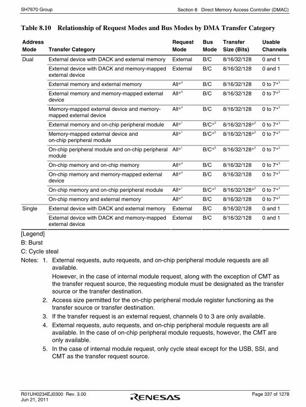
Section 8 Direct Memory Access Controller (DMAC)
R01UH0234EJ0300 Rev. 3.00 Page 337 of 1278 Jun 21, 2011
SH7670 Group
Table 8.10 Relationship of Request Modes and Bus Modes by DMA Transfer Category
Address Mode Transfer Category
Request Mode
Bus Mode
Transfer Size (Bits)
Usable Channels
External device with DACK and external memory External B/C 8/16/32/128 0 and 1
External device with DACK and memory-mapped external device
External B/C 8/16/32/128 0 and 1
External memory and external memory All*4 B/C 8/16/32/128 0 to 7*3
External memory and memory-mapped external device
All*4 B/C 8/16/32/128 0 to 7*3
Memory-mapped external device and memory-mapped external device
All*4 B/C 8/16/32/128 0 to 7*3
External memory and on-chip peripheral module All*1 B/C*5 8/16/32/128*2 0 to 7*3
Memory-mapped external device and on-chip peripheral module
All*1 B/C*5 8/16/32/128*2 0 to 7*3
On-chip peripheral module and on-chip peripheral module
All*1 B/C*5 8/16/32/128*2 0 to 7*3
On-chip memory and on-chip memory All*4 B/C 8/16/32/128 0 to 7*3
On-chip memory and memory-mapped external device
All*4 B/C 8/16/32/128 0 to 7*3
On-chip memory and on-chip peripheral module All*1 B/C*5 8/16/32/128*2 0 to 7*3
Dual
On-chip memory and external memory All*4 B/C 8/16/32/128 0 to 7*3
External device with DACK and external memory External B/C 8/16/32/128 0 and 1 Single
External device with DACK and memory-mapped external device
External B/C 8/16/32/128 0 and 1
[Legend]
B: Burst C: Cycle steal
Notes: 1. External requests, auto requests, and on-chip peripheral module requests are all available.
However, in the case of internal module request, along with the exception of CMT as the transfer request source, the requesting module must be designated as the transfer source or the transfer destination.
2. Access size permitted for the on-chip peripheral module register functioning as the transfer source or transfer destination.
3. If the transfer request is an external request, channels 0 to 3 are only available.
4. External requests, auto requests, and on-chip peripheral module requests are all available. In the case of on-chip peripheral module requests, however, the CMT are only available.
5. In the case of internal module request, only cycle steal except for the USB, SSI, and CMT as the transfer request source.

Section 8 Direct Memory Access Controller (DMAC)
Page 338 of 1278 R01UH0234EJ0300 Rev. 3.00 Jun 21, 2011
SH7670 Group
(4) Bus Mode and Channel Priority
In priority fixed mode (CH0 > CH1), when channel 1 is transferring data in burst mode and a request arrives for transfer on channel 0, which has higher-priority, the data transfer on channel 0 will begin immediately. In this case, if the transfer on channel 0 is also in burst mode, the transfer on channel 1 will only resume on completion of the transfer on channel 0.
When channel 0 is in cycle steal mode, one transfer-unit of data on this channel, which has the higher priority, is transferred. Data is then transferred continuously to channel 1 without releasing the bus. The bus mastership will then switch between the two in this order: channel 0, channel 1, channel 0, channel 1, etc. That is, the CPU cycle after the data transfer in cycle steal mode is replaced with a burst-mode transfer cycle (priority execution of burst-mode cycle). An example of this is shown in figure 8.12.
When multiple channels are in burst mode, data transfer on the channel that has the highest priority is given precedence. When DMA transfer is being performed on multiple channels, the bus mastership is not released to another bus-master device until all of the competing burst-mode transfers have been completed.
CPU DMACH1
DMACH1
DMACH0
DMACH1
DMACH0
DMACH1
DMACH1
CPU
CH0 CH1 CH0
DMAC CH0 and CH1Cycle steal mode
DMAC CH1Burst mode CPUCPU
Priority: CH0 > CH1CH0: Cycle steal mode CH1: Burst mode
DMAC CH1Burst mode
Figure 8.12 Bus State when Multiple Channels are Operating
In round-robin mode, the priority changes as shown in figure 8.3. Note that channels in cycle steal and burst modes must not be mixed.

Section 8 Direct Memory Access Controller (DMAC)
R01UH0234EJ0300 Rev. 3.00 Page 339 of 1278 Jun 21, 2011
SH7670 Group
8.4.5 Number of Bus Cycles and DREQ Pin Sampling Timing
(1) Number of Bus Cycles
When the DMAC is the bus master, the number of bus cycles is controlled by the bus state controller (BSC) in the same way as when the CPU is the bus master. For details, see section 7, Bus State Controller (BSC).
(2) DREQ Pin Sampling Timing
Figures 8.13 to 8.16 show the DREQ input sampling timings in each bus mode.
CKIO
DREQ
DACK
Bus cycle
(Rising)
(Active-high)
1st acceptance 2nd acceptance
CPU CPUCPU
Acceptance start
DMAC
Non sensitive period
Figure 8.13 Example of DREQ Input Detection in Cycle Steal Mode Edge Detection
CKIO
DREQ(Overrun 0 athigh level)
DACK(Active-high)
Bus cycle
1st acceptance
CPU CPUCPU DMAC
CKIO
DREQ(Overrun 1 athigh level)
DACK(Active-high)
Bus cycle
2nd acceptance
CPU CPUCPU DMAC
Acceptancestart
Acceptancestart
2nd acceptance
1st acceptance
Non sensitive period
Non sensitive period
Figure 8.14 Example of DREQ Input Detection in Cycle Steal Mode Level Detection

Section 8 Direct Memory Access Controller (DMAC)
Page 340 of 1278 R01UH0234EJ0300 Rev. 3.00 Jun 21, 2011
SH7670 Group
CKIO
DREQ(Rising)
DACK(Active-high)
Bus cycle
Burst acceptance
Non sensitive period
CPU CPU DMAC DMAC
Figure 8.15 Example of DREQ Input Detection in Burst Mode Edge Detection
CKIO
DREQ(Overrun 0 athigh level)
DACK(Active-high)
Bus cycle2ndacceptance
CPU CPU DMAC
CKIO
DREQ(Overrun 1 athigh level)
DACK(Active-high)
Bus cycle
1st acceptance
2nd acceptanceNon sensitive period
Non sensitive period
CPU CPU DMAC3rdacceptance
DMAC
Acceptancestart
Acceptancestart
Acceptancestart
1st acceptance
Figure 8.16 Example of DREQ Input Detection in Burst Mode Level Detection

Section 8 Direct Memory Access Controller (DMAC)
R01UH0234EJ0300 Rev. 3.00 Page 341 of 1278 Jun 21, 2011
SH7670 Group
Figure 8.17 shows the TEND output timing.
CKIO
DACK
DREQ
TEND
Bus cycle
End of DMA transfer
DMAC CPU CPUCPU DMAC
Figure 8.17 Example of DMA Transfer End Signal Timing (Cycle Steal Mode Level Detection)
The unit of the DMA transfer is divided into multiple bus cycles when 16-byte transfer is performed for an 8-bit, 16-bit, or 32-bit external device, when longword access is performed for an 8-bit or 16-bit external device, or when word access is performed for an 8-bit external device. When a setting is made so that the DMA transfer size is divided into multiple bus cycles and the CS signal is negated between bus cycles, note that DACK and TEND are divided like the CS signal for data alignment as shown in figure 8.18. Figures 8.13 to 8.17 show cases in which DACK and TEND are not divided at the time of DMA transfer.
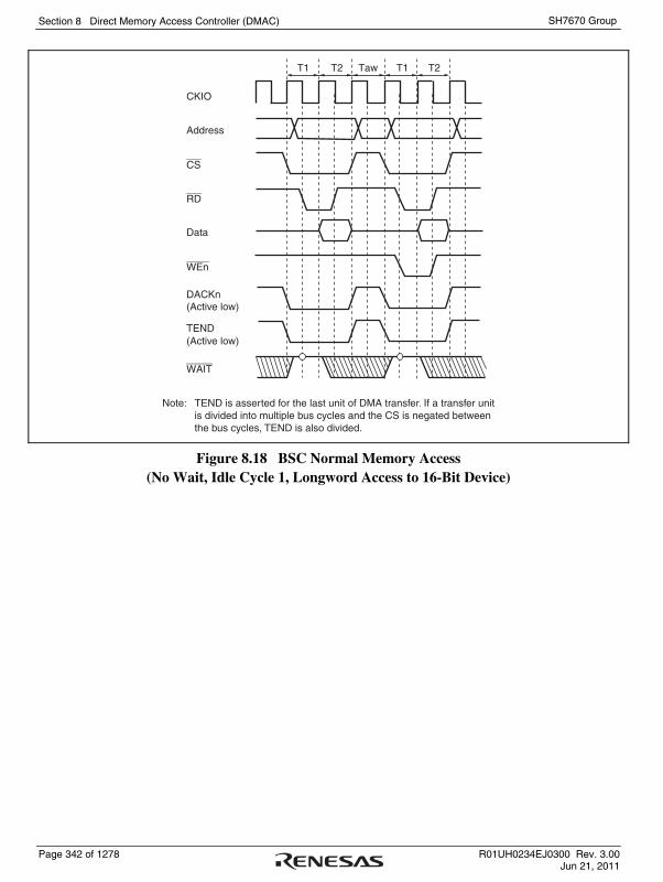
Section 8 Direct Memory Access Controller (DMAC)
Page 342 of 1278 R01UH0234EJ0300 Rev. 3.00 Jun 21, 2011
SH7670 Group
CKIO
Address
RD
Data
WEn
WAIT
CS
T1 T2 Taw T1 T2
DACKn(Active low)
TEND(Active low)
Note: TEND is asserted for the last unit of DMA transfer. If a transfer unitis divided into multiple bus cycles and the CS is negated betweenthe bus cycles, TEND is also divided.
Figure 8.18 BSC Normal Memory Access (No Wait, Idle Cycle 1, Longword Access to 16-Bit Device)
Section 8 Direct Memory Access Controller (DMAC)
R01UH0234EJ0300 Rev. 3.00 Page 343 of 1278 Jun 21, 2011
SH7670 Group
8.5 Usage Notes
8.5.1 NMIF Bit (NMI Flag) in DMA Operation Register (DMAOR)
When the flag is read with the same timing as flag setting, the flag is read as 0 but internally the LSI might enter the state where 1 has been read in some cases. Accordingly, if 0 is written to the flag in this state, the flag is cleared to 0 in the same way as when 0 is written to the flag after 1 is read.
When using this flag, take the following steps to read from and write to the flag to prevent unexpected clearing of the flag.
Only when explicitly clearing the flag, write 0 to the flag after reading 1; in other cases, the write value should always be 1.
When the flag is not used, the write value should always be 0 (write 0 after reading 1 only when explicitly clearing the flag).
8.5.2 Half-End Flag Setting and Half-End Interrupt Generation
Note the following when the half-end flag in CHCR is referred to or the half-end interrupt is used while the reload function is used.
The reload transfer count (the RDMATCR setting) should be the same value as the initial transfer count (the DMATCR setting). If the initial DMATCR setting and the RDMATCR setting used for the second or later transfers differ, the half-end flag or interrupt might be set or generated before the transfer count reaches half of the specified value, or the half-end flag or interrupt might never be set or generated.
Section 8 Direct Memory Access Controller (DMAC)
Page 344 of 1278 R01UH0234EJ0300 Rev. 3.00 Jun 21, 2011
SH7670 Group

Section 9 Clock Pulse Generator (CPG)
R01UH0234EJ0300 Rev. 3.00 Page 345 of 1278 Jun 21, 2011
SH7670 Group
Section 9 Clock Pulse Generator (CPG)
This LSI has a clock pulse generator (CPG) that generates an internal clock (Iφ), a peripheral clock (Pφ), and a bus clock (Bφ). The CPG consists of a crystal oscillator, PLL circuits, and divider circuits.
9.1 Features
• Four clock operating modes
The mode can be selected from among the four clock operating modes (three clock operating modes in the wide temperature specifications) based on the frequency range to be used and the input clock type: the crystal resonator, the external clock, the crystal resonator for USB, or the external clock for USB.
• Three clocks generated independently
An internal clock (Iφ) for the CPU and cache; a peripheral clock (Pφ) for the on-chip peripheral modules; a bus clock (Bφ = CKIO) for the external bus interface
• Frequency change function
Internal and peripheral clock frequencies can be changed independently using the PLL (phase locked loop) circuits and divider circuits within the CPG. Frequencies are changed by software using frequency control register (FRQCR) settings.
• Power-down mode control
The clock can be stopped in sleep mode and software standby mode, and specific modules can be stopped using the module standby function. For details on clock control in the power-down modes, see section 11, Power-Down Modes.

Section 9 Clock Pulse Generator (CPG)
Page 346 of 1278 R01UH0234EJ0300 Rev. 3.00 Jun 21, 2011
SH7670 Group
Figure 9.1 shows a block diagram of the clock pulse generator.
USB_X1
PLL circuit
(× 8,12)
Crystal oscillator
On-chip oscillator
Peripheral bus
Bus interface
FRQCR
[Legend]
: Frequency control register
EXTAL
XTAL
MD_CLK1
MD_CLK0
FRQCR
CPG control unit
Clock frequency control circuit
Standby control circuit
USB_X2
× 1× 1/2× 1/3× 1/4× 1/6× 1/8× 1/12
Internal clock (Iφ: 200 MHz max. (regular specifications) 133.3 MHz max. (wide temperature specifications)
Bus clock(Bφ = CKIO: 100 MHz max. (regular specifications) 66.6 MHz max. (wide temperature specifications)
Peripheral clock(Pφ: 50 MHz max. (regular specifications) 33.3 MHz max. (wide temperature specifications)
Divider 2
× 1× 1/2× 1/4
Divider 1
CKIO
Crystal oscillator
Figure 9.1 Block Diagram of Clock Pulse Generator

Section 9 Clock Pulse Generator (CPG)
R01UH0234EJ0300 Rev. 3.00 Page 347 of 1278 Jun 21, 2011
SH7670 Group
The clock pulse generator blocks function as follows:
(1) Crystal Oscillator
The crystal oscillator is an oscillation circuit in which the crystal resonator is connected to the XTAL/EXTAL pin or USB_X1/USB_X2 pin. This can be used according to the clock operating mode.
(2) Divider 1
Divider 1 divides the frequency of one of the three clocks: the clock from the crystal resonator or the EXTAL pin, the clock from the CKIO pin, and the clock from the crystal resonator or the USB_X1 pin. The division ratio depends on the clock operating mode.
(3) PLL Circuit
The PLL circuit multiplies the frequency of the output from divider 1 by 8 or 12. The multiplication rate is set by the frequency control register. When this is done, the phase of the rising edge of the internal clock is controlled so that it will agree with the phase of the rising edge of the CKIO pin.
The input clock to be used depends on the clock operating mode. The clock operating mode is specified using the MD_CK0 and MD_CK1 pins. For details on the clock operating mode, see table 9.2.
(4) Divider 2
Divider 2 divides the frequency of output of the PLL circuit to generate an internal clock, a bus clock, and a peripheral clock. The internal clock can be 1 or 1/2 times the output frequency of the PLL circuit, and it should not be lower than the clock frequency on the CKIO pin. The peripheral clock can be 1/4, 1/6, 1/8, or 1/12 times the output frequency of the PLL circuit, and it should not be higher than the half of the clock frequency on the CKIO pin. The bus clock is automatically determined by hardware at the division ratio against the output frequency of the PLL circuit so that it will be 4 times the clock source (when clock mode = 0), 2 times (when clock mode = 1 or 3), or 1 times (when clock mode = 2).
(5) Clock Frequency Control Circuit
The clock frequency control circuit controls the clock frequency using the MD_CK0 and MD_CK1 pins and the frequency control register (FRQCR).

Section 9 Clock Pulse Generator (CPG)
Page 348 of 1278 R01UH0234EJ0300 Rev. 3.00 Jun 21, 2011
SH7670 Group
(6) Standby Control Circuit
The standby control circuit controls the states of the clock pulse generator and other modules during clock switching, or sleep or software standby mode.
In addition, the standby control register is provided to control the power-down mode of other modules. For details on the standby control register, see section 11, Power-Down Modes.
(7) Frequency Control Register (FRQCR)
The frequency control register (FRQCR) has control bits assigned for the following functions: clock output/non-output from the CKIO pin during software standby mode, the frequency multiplication ratio of PLL circuit, and the frequency division ratio of the internal clock and the peripheral clock (Pφ).
Section 9 Clock Pulse Generator (CPG)
R01UH0234EJ0300 Rev. 3.00 Page 349 of 1278 Jun 21, 2011
SH7670 Group
9.2 Input/Output Pins
Table 9.1 lists the clock pulse generator pins and their functions.
Table 9.1 Pin Configuration and Functions of the Clock Pulse Generator
Pin Name Symbol I/O
Function (Clock Operating Mode 0)
Function (Clock Operating Mode 1)
Function (Clock Operating Mode 2)
Function (Clock Operating Mode 3)
MD_ CLK0
Input Sets the clock operating mode. Mode control pins
MD_ CLK1
Input Sets the clock operating mode.
XTAL Output Connected to the crystal resonator. (Leave this pin open when the crystal resonator is not in use.)
Leave this pin open.
Leave this pin open.
Leave this pin open.
Crystal input/output pins (clock input pins)
EXTAL Input Connected to the crystal resonator or used to input external clock.
Used as an external clock input terminal.
Pull-up this pin. Pull-up this pin.
Clock input/output pin
CKIO I/O Clock output pin.
Clock output pin
Clock input pin Clock output pin

Section 9 Clock Pulse Generator (CPG)
Page 350 of 1278 R01UH0234EJ0300 Rev. 3.00 Jun 21, 2011
SH7670 Group
Pin Name Symbol I/O
Function (Clock Operating Mode 0)
Function (Clock Operating Mode 1)
Function (Clock Operating Mode 2)
Function (Clock Operating Mode 3)
Crystal input/output pins for USB (clock input pins)
USB_X1 Input Connected to the crystal resonator to input the clock for USB only, or used to input external clock. When USB is not used, this pin should be pulled up.
Connected to the crystal resonator to input the clock for USB only, or used to input external clock. When USB is not used, this pin should be pulled up.
Connected to the crystal resonator to input the clock for USB only, or used to input external clock. When USB is not used, this pin should be pulled up.
Connected to the crystal resonator to input the clock for both USB and the LSI, or used to input external clock.
USB_X2 Output Connected to the crystal resonator for USB. (Leave this pin open when the crystal resonator is not in use.)
Connected to the crystal resonator for USB. (Leave this pin open when the crystal resonator is not in use.)
Connected to the crystal resonator for USB. (Leave this pin open when the crystal resonator is not in use.)
Connected to the crystal resonator for both USB and the LSI. (Leave this pin open when the crystal resonator is not in use.)

Section 9 Clock Pulse Generator (CPG)
R01UH0234EJ0300 Rev. 3.00 Page 351 of 1278 Jun 21, 2011
SH7670 Group
9.3 Clock Operating Modes
Table 9.2 shows the relationship between the combinations of the mode control pins (MD_CK1 and MD_CK0) and the clock operating modes. Table 9.3 shows the usable frequency ranges in the clock operating modes.
Table 9.2 Clock Operating Modes
Pin Values Clock I/O
Mode MD_CK1 MD_CK0 Source Output Divider 2PLL Circuit On/Off CKIO Frequency
0 0 0 EXTAL or crystal resonator
CKIO 1 ON (× 8, 12) (EXTAL or crystal resonator) × 4
1 0 1 EXTAL CKIO 1/2 ON (× 8, 12) (EXTAL) × 2
2 1 0 CKIO ⎯ 1/4 ON (× 8, 12) (CKIO)
3 1 1 USB_X1 or crystal resonator
CKIO 1/2 ON (× 8) (USB_X1 or crystal resonator) × 2
• Mode 0
In mode 0, clock is input from the EXTAL pin or the crystal resonator. The PLL circuit shapes waveforms and the frequency is multiplied according to the frequency control register setting before the clock is supplied to the LSI. The oscillating frequency for the crystal resonator and EXTAL pin input clock ranges from 15 to 25 MHz (15 to 16.6 MHz in the wide temperature specifications). The frequency range of CKIO is from 60 to 100 MHz (60 MHz to 66.6 MHz in the wide temperature specifications). To reduce current supply, pull up the USB_X1 pin and open the USB_X2 pin when USB is not used.
• Mode 1
In mode 1, clock is input from the EXTAL pin. The PLL circuit shapes waveform and the frequency is multiplied according to the frequency control register setting before the clock is supplied to the LSI. The oscillating frequency for the EXTAL pin input clock ranges from 30 to 50 MHz (30 to 33.3 MHz in the wide temperature specifications). The frequency range of CKIO is from 60 to 100 MHz (60 to 66.6 MHz in the wide temperature specifications). To reduce current supply, pull up the USB_X1 pin and open the USB_X2 pin when USB is not used.
Section 9 Clock Pulse Generator (CPG)
Page 352 of 1278 R01UH0234EJ0300 Rev. 3.00 Jun 21, 2011
SH7670 Group
• Mode 2
In mode 2, the CKIO pin functions as an input pin and draws an external clock signal. The PLL circuit shapes waveform and the frequency is multiplied according to the frequency control register setting before the clock is supplied to the LSI. The frequency range of CKIO is from 60 to 100 MHz (60 to 66.6 MHz in the wide temperature specifications). To reduce current supply, pull up the EXTAL pin and open the XTAL pin when the LSI is used in mode 2. When USB is not used, pull up the USB_X1 pin and open the USB_X2 pin.
• Mode 3
In mode 3, clock is input from the USB_X1 pin or the crystal oscillator. The external clock is input through this pin and waveform is shaped in the PLL circuit. Then the frequency is multiplied according to the frequency control register setting before the clock is supplied to the LSI. The frequency of CKIO is the same as that of the input clock 96 MHz. To reduce current supply, pull up the EXTAL pin and open the XTAL pin when the LSI is used in mode 3. When the USB crystal resonator is not used, open the USB_X2 pin.
Note that this mode is supported only in the regular specifications; it is not supported in the wide temperature specifications.
Table 9.3 Relationship between Clock Operating Mode and Frequency Range (1)
Regular Specifications
Restrictions: Iφ ≤ 200MHz, Bφ ≤ 100MHz, Pφ ≤ 50MHz, Iφ ≤ Bφ ≤ Pφ×2
PLL
Frequency
Multiplier Selectable Frequency Range (MHz) Clock
Operating
Mode
FRQCR
Setting*1 Divider 1
PLL
Circuit
Ratio of
Internal
Clock
Frequencies
(I:B:P)*2 Input Clock*3
Output Clock
(CKIO Pin)
Internal Clock
(Iφ)
Bus Clock
(Bφ)
Peripheral
Clock (Pφ)
H'x003 1/1 ON (× 8) 8:4:2 15.00 to 25.00 60.00 to 100.00 120.00 to 200.00 60.00 to 100.00 30.00 to 50.00
H'x004 1/1 ON (× 8) 8:4:4/3 15.00 to 25.00 60.00 to 100.00 120.00 to 200.00 60.00 to 100.00 20.00 to 33.33
H'x005 1/1 ON (× 8) 8:4:1 15.00 to 25.00 60.00 to 100.00 120.00 to 200.00 60.00 to 100.00 15.00 to 25.00
H'x006 1/1 ON (× 8) 8:4:2/3 15.00 to 25.00 60.00 to 100.00 120.00 to 200.00 60.00 to 100.00 10.00 to 16.67
H'x013 1/1 ON (× 8) 4:4:2 15.00 to 25.00 60.00 to 100.00 60.00 to 100.00 60.00 to 100.00 30.00 to 50.00
H'x014 1/1 ON (× 8) 4:4:4/3 15.00 to 25.00 60.00 to 100.00 60.00 to 100.00 60.00 to 100.00 20.00 to 33.33
H'x015 1/1 ON (× 8) 4:4:1 15.00 to 25.00 60.00 to 100.00 60.00 to 100.00 60.00 to 100.00 15.00 to 25.00
H'x016 1/1 ON (× 8) 4:4:2/3 15.00 to 25.00 60.00 to 100.00 60.00 to 100.00 60.00 to 100.00 10.00 to 16.67
H'x104 1/1 ON (× 12) 12:4:2 15.00 to 16.67 60.00 to 66.67 180.00 to 200.00 60.00 to 66.67 30.00 to 33.33
0
H'x106 1/1 ON (× 12) 12:4:1 15.00 to 16.67 60.00 to 66.67 180.00 to 200.00 60.00 to 66.67 15.00 to 16.67

Section 9 Clock Pulse Generator (CPG)
R01UH0234EJ0300 Rev. 3.00 Page 353 of 1278 Jun 21, 2011
SH7670 Group
PLL
Frequency
Multiplier Selectable Frequency Range (MHz) Clock
Operating
Mode
FRQCR
Setting*1 Divider 1
PLL
Circuit
Ratio of
Internal
Clock
Frequencies
(I:B:P)*2 Input Clock*3
Output Clock
(CKIO Pin)
Internal Clock
(Iφ)
Bus Clock
(Bφ)
Peripheral
Clock (Pφ)
H'x003 1/2 ON (× 8) 4:2:1 30.00 to 50.00 60.00 to 100.00 120.00 to 200.00 60.00 to 100.00 30.00 to 50.00
H'x004 1/2 ON (× 8) 4:2:4/3 30.00 to 50.00 60.00 to 100.00 120.00 to 200.00 60.00 to 100.00 20.00 to 33.33
H'x005 1/2 ON (× 8) 4:2:1/2 30.00 to 50.00 60.00 to 100.00 120.00 to 200.00 60.00 to 100.00 15.00 to 25.00
H'x006 1/2 ON (× 8) 4:1:1/3 30.00 to 50.00 60.00 to 100.00 120.00 to 200.00 60.00 to 100.00 10.00 to 16.67
H'x013 1/2 ON(× 8) 2:2:1 30.00 to 50.00 60.00 to 100.00 60.00 to 100.00 60.00 to 100.00 30.00 to 50.00
H'x014 1/2 ON(× 8) 2:2:2/3 30.00 to 50.00 60.00 to 100.00 60.00 to 100.00 60.00 to 100.00 20.00 to 33.33
H'x015 1/2 ON(× 8) 2:2:1/2 30.00 to 50.00 60.00 to 100.00 60.00 to 100.00 60.00 to 100.00 15.00 to 25.00
H'x016 1/2 ON(× 8) 2:2:1/3 30.00 to 50.00 60.00 to 100.00 60.00 to 100.00 60.00 to 100.00 10.00 to 16.67
H'x104 1/2 ON (× 12) 6:2:1 30.00 to 33.33 60.00 to 66.67 180.00 to 200.00 60.00 to 66.67 30.00 to 33.33
1
H'x106 1/2 ON (× 12) 6:2:1/2 30.00 to 33.33 60.00 to 66.67 180.00 to 200.00 60.00 to 66.67 15.00 to 16.67
H'x003 1/4 ON (× 8) 2:1:1/2 60.00 to 100.00 ⎯ 120.00 to 200.00 60.00 to 100.00 30.00 to 50.00
H'x004 1/4 ON (× 8) 2:1:1/3 60.00 to 100.00 ⎯ 120.00 to 200.00 60.00 to 100.00 20.00 to 33.33
H'x005 1/4 ON (× 8) 2:1:1/4 60.00 to 100.00 ⎯ 120.00 to 200.00 60.00 to 100.00 15.00 to 25.00
H'x006 1/4 ON (× 8) 2:1:1/6 60.00 to 100.00 ⎯ 120.00 to 200.00 60.00 to 100.00 10.00 to 16.67
H'x013 1/4 ON (× 8) 1:1:1/2 60.00 to 100.00 ⎯ 60.00 to 100.00 60.00 to 100.00 30.00 to 50.00
H'x014 1/4 ON (× 8) 1:1:1/3 60.00 to 100.00 ⎯ 60.00 to 100.00 60.00 to 100.00 20.00 to 33.33
H'x015 1/4 ON (× 8) 1:1:1/4 60.00 to 100.00 ⎯ 60.00 to 100.00 60.00 to 100.00 15.00 to 25.00
H'x016 1/4 ON (× 8) 1:1:1/6 60.00 to 100.00 ⎯ 60.00 to 100.00 60.00 to 100.00 10.00 to 16.67
H'x104 1/4 ON (× 12) 3:1:1/2 60.00 to 66.67 ⎯ 180.00 to 200.00 60.00 to 66.67 30.00 to 33.33
2
H'x106 1/4 ON (× 12) 3:1:1/4 60.00 to 66.67 ⎯ 180.00 to 200.00 60.00 to 66.67 15.00 to 16.67
H'x003 1/2 ON (× 8) 4:2:1 48.00 to 48.00 96.00 to 96.00 192.00 to 192.00 96.00 to 96.00 48.00 to 48.00
H'x004 1/2 ON (× 8) 4:2:2/3 48.00 to 48.00 96.00 to 96.00 192.00 to 192.00 96.00 to 96.00 32.00 to 32.00
H'x005 1/2 ON (× 8) 4:2:1/2 48.00 to 48.00 96.00 to 96.00 192.00 to 192.00 96.00 to 96.00 24.00 to 24.00
H'x006 1/2 ON (× 8) 4:2:1/3 48.00 to 48.00 96.00 to 96.00 192.00 to 192.00 96.00 to 96.00 16.00 to 16.00
H'x013 1/2 ON (× 8) 2:2:1 48.00 to 48.00 96.00 to 96.00 96.00 to 96.00 96.00 to 96.00 48.00 to 48.00
H'x014 1/2 ON (× 8) 2:2:2/3 48.00 to 48.00 96.00 to 96.00 96.00 to 96.00 96.00 to 96.00 32.00 to 32.00
H'x015 1/2 ON (× 8) 2:2:1/2 48.00 to 48.00 96.00 to 96.00 96.00 to 96.00 96.00 to 96.00 24.00 to 24.00
3
H'x016 1/2 ON (× 8) 2:2:1/3 48.00 to 48.00 96.00 to 96.00 96.00 to 96.00 96.00 to 96.00 16.00 to 16.00

Section 9 Clock Pulse Generator (CPG)
Page 354 of 1278 R01UH0234EJ0300 Rev. 3.00 Jun 21, 2011
SH7670 Group
Table 9.3 Relationship between Clock Operating Mode and Frequency Range (2)
wide temperature Specifications
Restrictions: Iφ ≤ 200MHz, Bφ ≤ 100MHz, Pφ ≤ 50MHz, Iφ ≤ Bφ ≤ Pφ×2
PLL
Frequency
Multiplier Selectable Frequency Range (MHz) Clock
Operating
Mode
FRQCR
Setting*1
Divider
1
PLL
Circuit
Ratio of
Internal
Clock
Frequencies
(I:B:P)*2 Input Clock*3
Output Clock
(CKIO Pin)
Internal Clock
(Iφ)
Bus Clock
(Bφ)
Peripheral
Clock (Pφ)
H'x003 1/1 ON (× 8) 8/4/2 15.00 to 16.67 60.00 to 66.67 120.00 to 133.33 60.00 to 66.67 30.00 to 33.33
H'x004 1/1 ON (× 8) 8/4/4/3 15.00 to 16.67 60.00 to 66.67 120.00 to 133.33 60.00 to 66.67 20.00 to 22.22
H'x005 1/1 ON (× 8) 8/4/1 15.00 to 16.67 60.00 to 66.67 120.00 to 133.33 60.00 to 66.67 15.00 to 16.67
H'x006 1/1 ON (× 8) 8/4/2/3 15.00 to 16.67 60.00 to 66.67 120.00 to 133.33 60.00 to 66.67 10.00 to 11.11
H'x013 1/1 ON (× 8) 4/4/2 15.00 to 16.67 60.00 to 66.67 60.00 to 66.67 60.00 to 66.67 30.00 to 33.33
H'x014 1/1 ON (× 8) 4/4/4/3 15.00 to 16.67 60.00 to 66.67 60.00 to 66.67 60.00 to 66.67 20.00 to 22.22
H'x015 1/1 ON (× 8) 4/4/1 15.00 to 16.67 60.00 to 66.67 60.00 to 66.67 60.00 to 66.67 15.00 to 16.67
0
H'x016 1/1 ON (× 8) 4/4/2/3 15.00 to 16.67 60.00 to 66.67 60.00 to 66.67 60.00 to 66.67 10.00 to 11.11
H'x003 1/2 ON (× 8) 4/2/1 30.00 to 33.33 60.00 to 66.67 120.00 to 133.33 60.00 to 66.67 30.00 to 33.33
H'x004 1/2 ON (× 8) 4/2/2/3 30.00 to 33.33 60.00 to 66.67 120.00 to 133.33 60.00 to 66.67 20.00 to 22.22
H'x005 1/2 ON (× 8) 4/2/1/2 30.00 to 33.33 60.00 to 66.67 120.00 to 133.33 60.00 to 66.67 15.00 to 16.67
H'x006 1/2 ON (× 8) 4/2/1/3 30.00 to 33.33 60.00 to 66.67 120.00 to 133.33 60.00 to 66.67 10.00 to 11.11
H'x013 1/2 ON (× 8) 2/2/1 30.00 to 33.33 60.00 to 66.67 60.00 to 66.67 60.00 to 66.67 30.00 to 33.33
H'x014 1/2 ON (× 8) 2/2/2/3 30.00 to 33.33 60.00 to 66.67 60.00 to 66.67 60.00 to 66.67 20.00 to 22.22
H'x015 1/2 ON (× 8) 2/2/1/2 30.00 to 33.33 60.00 to 66.67 60.00 to 66.67 60.00 to 66.67 15.00 to 16.67
1
H'x016 1/2 ON (× 8) 2/2/1/3 30.00 to 33.33 60.00 to 66.67 60.00 to 66.67 60.00 to 66.67 10.00 to 11.11
H'x003 1/4 ON (× 8) 2/1/1/2 60.00 to 66.67 ⎯ 120.00 to 133.33 60.00 to 66.67 30.00 to 33.33
H'x004 1/4 ON (× 8) 2/1/1/3 60.00 to 66.67 ⎯ 120.00 to 133.33 60.00 to 66.67 20.00 to 22.22
H'x005 1/4 ON (× 8) 2/1/1/4 60.00 to 66.67 ⎯ 120.00 to 133.33 60.00 to 66.67 15.00 to 16.67
H'x006 1/4 ON (× 8) 2/1/1/6 60.00 to 66.67 ⎯ 120.00 to 133.33 60.00 to 66.67 10.00 to 11.11
H'x013 1/4 ON (× 8) 1/1/1/2 60.00 to 66.67 ⎯ 60.00 to 66.67 60.00 to 66.67 30.00 to 33.33
H'x014 1/4 ON (× 8) 1/1/1/3 60.00 to 66.67 ⎯ 60.00 to 66.67 60.00 to 66.67 20.00 to 22.22
H'x015 1/4 ON (× 8) 1/1/1/4 60.00 to 66.67 ⎯ 60.00 to 66.67 60.00 to 66.67 15.00 to 16.67
2
H'x016 1/4 ON (× 8) 1/1/1/6 60.00 to 66.67 ⎯ 60.00 to 66.67 60.00 to 66.67 10.00 to 11.11
Notes: 1. x in the FRQCR register setting depends on the set value in bits 12 and 13.
2. The ratio of clock frequencies, where the input clock frequency is assumed to be 1.

Section 9 Clock Pulse Generator (CPG)
R01UH0234EJ0300 Rev. 3.00 Page 355 of 1278 Jun 21, 2011
SH7670 Group
3. In mode 0, the frequency of the EXTAL pin input clock or the crystal resonator
In mode 1, the frequency of the EXTAL pin input clock In mode 2, the frequency of the CKIO pin input clock.
In mode 3, the frequency of the USB_X1 pin input clock or the crystal resonator
Cautions: 1. The frequency of the internal clock is as follows:
In mode 0 the frequency on the EXTAL pin × the frequency-multiplier of the PLL circuit × the divisor of the divider 1
In mode 1 (the frequency on the EXTAL pin × 1/2) × the frequency-multiplier of the PLL circuit × the divisor of the divider 1
In mode 2 (the frequency on the CKIO pin × 1/4) × the frequency-multiplier of the PLL circuit × the divisor of the divider 1
In mode 3 (the frequency on the USB_X1pin × 1/2) × the frequency-multiplier of the PLL circuit × the divisor of the divider 1
The frequency of the internal clock should not be set lower than the frequency on the CKIO pin.
2. The frequency of the peripheral clock is as follows:
In mode 0 the frequency on the EXTAL pin × the frequency-multiplier of the PLL circuit × the divisor of the divider 1 In mode 1 (the frequency on the EXTAL pin × 1/2) × the frequency-multiplier of the PLL circuit × the divisor of the divider 1
In mode 2 (the frequency on the CKIO pin × 1/4) × the frequency-multiplier of the PLL circuit × the divisor of the divider 1
In mode 3 (the frequency on the USB_X1 pin × 1/2) × the frequency-multiplier of the PLL circuit × the divisor of the divider 1
The frequency of the peripheral clock should be set to 50 MHz or less, and should not be set higher than one half of the frequency on the CKIO pin.
3. The frequency multiplier of PLL circuit can be selected as ×8 or × 12. The divisor of the divider can be selected as × 1, × 1/2, × 1/3, × 1/4, × 1/6, × 1/8, or × 1/12. The settings are made in the frequency-control register (FRQCR).
4. The output frequency of the PLL circuit is as follows: In mode 0 the frequency on the EXTAL pin × the frequency-multiplier of the PLL
circuit In mode 1 (the frequency on the EXTAL pin × 1/2) × the frequency-multiplier of
the PLL circuit In mode 2 (the frequency on the CKIO pin × 1/4) × the frequency-multiplier of
the PLL circuit In mode 3 (the frequency on the USB_X1 pin × 1/2) × the frequency-multiplier of
the PLL circuit Ensure that the output frequency of the PLL circuit should be 200 MHz or less.

Section 9 Clock Pulse Generator (CPG)
Page 356 of 1278 R01UH0234EJ0300 Rev. 3.00 Jun 21, 2011
SH7670 Group
9.4 Register Descriptions
The clock pulse generator has the following registers.
Table 9.4 Register Configuration
Register Name Abbreviation R/W Initial Value Address Access Size
Frequency control register FRQCR R/W H'0003 H'FFFE0010 16
9.4.1 Frequency Control Register (FRQCR)
FRQCR is a 16-bit readable/writable register used to specify whether a clock is output from the CKIO pin during normal operation mode, software standby mode and standby mode cancellation. The register also specifies the frequency-multiplier of the PLL circuit and the frequency division ratio for the internal clock and peripheral clock (Pφ). FRQCR is accessed by word.
FRQCR is initialized to H'0003 only by a power-on reset or in deep standby. FRQCR retains its previous value in manual reset or software standby mode. The previous value is also retained when an internal reset is triggered by an overflow of the WDT.
15 14 13 12 11 10 9 8 7 6 5 4 3 2 1 0
0 0 0 0 0 0 0 0 0 0 0 0 0 0 1 1R R R/W R/W R R R/W R/W R R R R/W R R/W R/W R/W
Bit:
Initial value:R/W:
- - CKOEN[1:0] - STC[1:0] - - IFC - PFC[2:0]- --
Bit Bit Name Initial Value R/W Description
15, 14 ⎯ All 0 R Reserved
These bits are always read as 0. The write value should always be 0.

Section 9 Clock Pulse Generator (CPG)
R01UH0234EJ0300 Rev. 3.00 Page 357 of 1278 Jun 21, 2011
SH7670 Group
Bit Bit Name Initial Value R/W Description
13, 12 CKOEN[1:0] 00 R/W Clock Output Enable
Specifies the CKIO pin outputs clock signals, or is set to a fixed level or high impedance (Hi-Z) during normal operation mode, standby mode, or cancellation of standby mode.
If these bits are set to 01, the CKIO pin is fixed at low during standby mode or cancellation of standby mode. Therefore, the malfunction of an external circuit caused by an unstable CKIO clock during cancellation of standby mode can be prevented. In clock operating mode 2, the CKIO pin functions as an input regardless of the value of these bits.
In normal operation In standby mode
00 Output Output off (Hi-Z)
01 Output Low-level output
10 Output Output (unstable clock output)
11 Output off (Hi-Z) Output off (Hi-Z) 11, 10 ⎯ All 0 R Reserved
These bits are always read as 0. The write value should always be 0.
9, 8 STC[1:0] 00 R/W Frequency Multiplication Ratio of PLL Circuit
00: × 8 time
01: × 12 times
10: Reserved (setting prohibited)
11: Reserved (setting prohibited)
7 to 5 ⎯ All 0 R Reserved
These bits are always read as 0. The write value should always be 0.

Section 9 Clock Pulse Generator (CPG)
Page 358 of 1278 R01UH0234EJ0300 Rev. 3.00 Jun 21, 2011
SH7670 Group
Bit Bit Name Initial Value R/W Description
4 IFC 0 R/W Internal Clock Frequency Division Ratio
This bit specifies the frequency division ratio of the internal clock with respect to the output frequency of PLL circuit.
0: × 1 time
1: × 1/2 time
3 ⎯ 0 R Reserved
This bit is always read as 0. The write value should always be 0.
2 to 0 PFC[2:0] 011 R/W Peripheral Clock Frequency Division Ratio
These bits specify the frequency division ratio of the peripheral clock with respect to the output frequency of PLL circuit.
000: Reserved (setting prohibited)
001: Reserved (setting prohibited)
010: Reserved (setting prohibited)
011: × 1/4 time
100: × 1/6 time
101: × 1/8 time
110: × 1/12 time
111: Reserved (setting prohibited)

Section 9 Clock Pulse Generator (CPG)
R01UH0234EJ0300 Rev. 3.00 Page 359 of 1278 Jun 21, 2011
SH7670 Group
9.5 Changing the Frequency
The frequency of the internal clock (Iφ) and peripheral clock (Pφ) can be changed either by changing the multiplication rate of PLL circuit or by changing the division rates of divider. All of these are controlled by software through the frequency control register (FRQCR). The methods are described below.
9.5.1 Changing the Multiplication Rate
A PLL settling time is required when the multiplication rate of PLL circuit is changed. The on-chip WDT counts the settling time.
1. In the initial state, the multiplication rate of PLL circuit is 8 time.
2. Set a value that will become the specified oscillation settling time in the WDT and stop the WDT. The following must be set:
WTCSR.TME = 0: WDT stops
WTCSR.CKS[2:0]: Division ratio of WDT count clock
WTCNT counter: Initial counter value
(The WDT count is incremented using the clock after the setting.)
3. Set the desired value in the STC1 and STC0 bits. The division ratio can also be set in the IFC and PFC2 to PFC0 bits.
4. This LSI pauses temporarily and the WDT starts incrementing. The internal and peripheral clocks both stop and the WDT is supplied with the clock. The clock will continue to be output at the CKIO pin. This state is the same as software standby mode. Whether or not registers are initialized depends on the module. For details, see section 28.3, Register States in Each Operating Mode.
5. Supply of the clock that has been set begins at WDT count overflow, and this LSI begins operating again. The WDT stops after it overflows.

Section 9 Clock Pulse Generator (CPG)
Page 360 of 1278 R01UH0234EJ0300 Rev. 3.00 Jun 21, 2011
SH7670 Group
9.5.2 Changing the Division Ratio
Counting by the WDT does not proceed if the frequency divisor is changed but the multiplier is not.
1. In the initial state, IFC = B'0 and PFC[2:0] = B'011.
2. Set the desired value in the IFC and PFC2 to IFC0 bits. The values that can be set are limited by the clock operating mode and the multiplication rate of PLL circuit. Note that if the wrong value is set, this LSI will malfunction.
3. After the register bits (IFC and PFC2 to PFC0) have been set, the clock is supplied of the new division ratio.
Note: When executing the SLEEP instruction after the frequency has been changed, be sure to
read the frequency control register (FRQCR) three times before executing the SLEEP instruction.

Section 9 Clock Pulse Generator (CPG)
R01UH0234EJ0300 Rev. 3.00 Page 361 of 1278 Jun 21, 2011
SH7670 Group
9.6 Notes on Board Design
9.6.1 Note on Inputting External Clock
Figure 9.2 is an example of connecting the external clock input. When putting the XTAL pin in open state, make sure the parasitic capacitance is less than or equal to 10 pF. To stably input the external clock with enough PLL stabilizing time at power on or releasing the standby, wait longer than the oscillation stabilizing time.
EXTAL
XTAL
External clock input
Open state
Example of connection with XTAL pin open
Figure 9.2 Example of Connecting External Clock
9.6.2 Note on Using an External Crystal Resonator
Place the crystal resonator and capacitors CL1 and CL2 as close to the XTAL and EXTAL pins as possible. In addition, to minimize induction and thus obtain oscillation at the correct frequency, the capacitors to be attached to the resonator must be grounded to the same ground. Do not bring wiring patterns close to these components.
CL1 CL2
EXTAL XTAL
Signal lines prohibited
This LSI
The values for CL1 and CL2
should be determined after
consultation with the crystal
resonator manufacturer.
Note:
Reference value
CL1 = 10 pF
CL2 = 10 pF
Figure 9.3 Note on Using a Crystal Resonator

Section 9 Clock Pulse Generator (CPG)
Page 362 of 1278 R01UH0234EJ0300 Rev. 3.00 Jun 21, 2011
SH7670 Group
9.6.3 Note on Resonator
Since various characteristics related to the resonator are closely linked to the user’s board design, thorough evaluation is necessary on the user’s part, using the resonator connection examples shown in this section as a guide. As the parameters for the oscillation circuit will depend on the floating capacitance of the resonator and the user board, the parameters should be determined in consultation with the resonator manufacturer. The design must ensure that a voltage exceeding the maximum rating is not applied to the resonator pin.
9.6.4 Note on Using a PLL Oscillation Circuit
In the PLLVcc and PLLVss connection pattern for the PLL, signal lines from the board power supply pins must be as short as possible and pattern width must be as wide as possible to reduce inductive interference.
In clock operating mode 2 or 3, the EXTAL pin is pulled up and the XTAL pin is left open.
Since the analog power supply pins of the PLL are sensitive to the noise, the system may malfunction due to inductive interference at the other power supply pins. To prevent such malfunction, the analog power supply pins and digital power supply pins Vcc and VccQ should not supply the same resources on the board if at all possible.
PLLVcc
PLLVss
Vcc
Vss
Power supply
Signal lines prohibited
Figure 9.4 Note on Using a PLL Oscillation Circuit
Section 10 Watchdog Timer (WDT)
R01UH0234EJ0300 Rev. 3.00 Page 363 of 1278 Jun 21, 2011
SH7670 Group
Section 10 Watchdog Timer (WDT)
This LSI includes the watchdog timer (WDT), which externally outputs an overflow signal (WDTOVF) on overflow of the counter when the value of the counter has not been updated because of a system malfunction. The WDT can simultaneously generate an internal reset signal for the entire LSI.
The WDT is a single channel timer that counts up the clock oscillation settling period when the system leaves software standby mode or the temporary standby periods that occur when the clock frequency is changed. It can also be used as a general watchdog timer or interval timer.
10.1 Features
• Can be used to ensure the clock oscillation settling time
The WDT is used in leaving software standby mode or the temporary standby periods that occur when the clock frequency is changed.
• Can switch between watchdog timer mode and interval timer mode.
• Outputs WDTOVF signal in watchdog timer mode
When the counter overflows in watchdog timer mode, the WDTOVF signal is output externally. It is possible to select whether to reset the LSI internally when this happens. Either the power-on reset or manual reset signal can be selected as the internal reset type.
• Interrupt generation in interval timer mode
An interval timer interrupt is generated when the counter overflows.
• Choice of eight counter input clocks
Eight clocks (Pφ × 1 to Pφ × 1/16384) that are obtained by dividing the peripheral clock can be selected.

Section 10 Watchdog Timer (WDT)
Page 364 of 1278 R01UH0234EJ0300 Rev. 3.00 Jun 21, 2011
SH7670 Group
Figure 10.1 shows a block diagram of the WDT.
WDTOVF
WTCSR WTCNTWRCSR
WDT
Standbycontrol
Bus interface
Divider
Clock selector
Clock
Standbymode
Peripheralclock
Standbycancellation
Resetcontrol
Clock selection
OverflowInternal reset request*
Interruptcontrol
Interruptrequest
[Legend]WTCSR:WTCNT:WRCSR:
Watchdog timer control/status registerWatchdog timer counterWatchdog reset control/status register
Note: * The internal reset signal can be generated by making a register setting.
Figure 10.1 Block Diagram of WDT
10.2 Input/Output Pin
Table 10.1 shows the pin configuration of the WDT.
Table 10.1 Pin Configuration
Pin Name Symbol I/O Function
Watchdog timer overflow WDTOVF Output Outputs the counter overflow signal in watchdog timer mode

Section 10 Watchdog Timer (WDT)
R01UH0234EJ0300 Rev. 3.00 Page 365 of 1278 Jun 21, 2011
SH7670 Group
10.3 Register Descriptions
The WDT has the following registers.
Table 10.2 Register Configuration
Register Name Abbreviation R/W Initial Value Address
Access Size
Watchdog timer counter WTCNT R/W H'00 H'FFFE0002 16*
Watchdog timer control/status register
WTCSR R/W H'18 H'FFFE0000 16*
Watchdog reset control/status register
WRCSR R/W H'1F H'FFFE0004 16*
Note: * For the access size, see section 10.3.4, Notes on Register Access.
10.3.1 Watchdog Timer Counter (WTCNT)
WTCNT is an 8-bit readable/writable register that is incremented by cycles of the selected clock signal. When an overflow occurs, it generates a watchdog timer overflow signal (WDTOVF) in watchdog timer mode and an interrupt in interval timer mode. WTCNT is initialized to H'00 by a power-on reset caused by the RES pin or in software standby mode.
Use word access to write to WTCNT, writing H'5A in the upper byte. Use byte access to read from WTCNT.
Note: The method for writing to WTCNT differs from that for other registers to prevent erroneous writes. See section 10.3.4, Notes on Register Access, for details.
7 6 5 4 3 2 1 0
0 0 0 0 0 0 0 0R/W R/W R/W R/W R/W R/W R/W R/W
Bit:
Initial value:R/W:

Section 10 Watchdog Timer (WDT)
Page 366 of 1278 R01UH0234EJ0300 Rev. 3.00 Jun 21, 2011
SH7670 Group
10.3.2 Watchdog Timer Control/Status Register (WTCSR)
WTCSR is an 8-bit readable/writable register composed of bits to select the clock used for the count, overflow flags, and timer enable bit.
WTCSR is initialized to H'18 by a power-on reset caused by the RES pin or in software standby mode. When used to count the clock oscillation settling time for canceling software standby mode, it retains its value after counter overflow.
Use word access to write to WTCSR, writing H'A5 in the upper byte. Use byte access to read from WTCSR.
Note: The method for writing to WTCSR differs from that for other registers to prevent erroneous writes. See section 10.3.4, Notes on Register Access, for details.
7 6 5 4 3 2 1 0
0 0 0 1 1 0 0 0R/(W) R/W R/W R R R/W R/W R/W
Bit:
Initial value:R/W:
IOVF WT/IT TME - - CKS[2:0]
Bit Bit Name Initial Value R/W Description
7 IOVF 0 R/(W) Interval Timer Overflow
Indicates that WTCNT has overflowed in interval timer mode. This flag is not set in watchdog timer mode.
0: No overflow
1: WTCNT overflow in interval timer mode
[Clearing condition]
• When 0 is written to IOVF after reading IOVF
6 WT/IT 0 R/W Timer Mode Select
Selects whether to use the WDT as a watchdog timer or an interval timer.
0: Use as interval timer
1: Use as watchdog timer
Note: When the WTCNT overflows in watchdog timer mode, the WDTOVF signal is output externally.If this bit is modified when the WDT is running, the counting-up may not be performed correctly.

Section 10 Watchdog Timer (WDT)
R01UH0234EJ0300 Rev. 3.00 Page 367 of 1278 Jun 21, 2011
SH7670 Group
Bit Bit Name Initial Value R/W Description
5 TME 0 R/W Timer Enable
Starts and stops timer operation. Clear this bit to 0 when using the WDT in software standby mode or when changing the clock frequency.
0: Timer disabled
Count-up stops and WTCNT value is retained
1: Timer enabled
4, 3 ⎯ All 1 R Reserved
These bits are always read as 1. The write value should always be 1.
Clock Select
These bits select the clock to be used for the WTCNT count from the eight types obtainable by dividing the peripheral clock (Pφ). The overflow period that is shown inside the parenthesis in the table is the value when the peripheral clock (Pφ) is 25 MHz.
Bits 2 to 0 Clock Ratio Overflow Cycle
000: 1 × Pφ 10.2 μs
001: 1/64 × Pφ 655.4 μs
010: 1/128 × Pφ 1.3 ms
011: 1/256 × Pφ 2.6 ms
100: 1/512 × Pφ 5.2 ms
101: 1/1024 × Pφ 10.5 ms
110: 1/4096 × Pφ 41.9 ms
111: 1/16384 × Pφ 167.8 ms
2 to 0 CKS[2:0] 000 R/W
Note: If the CKS2 to CKS0 bits are modified when the WDT is running, the counting-up may not be performed correctly. Ensure that these bits are modified only when the WDT is not running.

Section 10 Watchdog Timer (WDT)
Page 368 of 1278 R01UH0234EJ0300 Rev. 3.00 Jun 21, 2011
SH7670 Group
10.3.3 Watchdog Reset Control/Status Register (WRCSR)
WRCSR is an 8-bit readable/writable register that controls output of the internal reset signal generated by watchdog timer counter (WTCNT) overflow.
WRCSR is initialized to H'1F by input of a reset signal from the RES pin, but is not initialized by the internal reset signal generated by overflow of the WDT. WRCSR is initialized to H'1F in software standby mode.
Note: The method for writing to WRCSR differs from that for other registers to prevent erroneous writes. See section 10.3.4, Notes on Register Access, for details.
7 6 5 4 3 2 1 0
0 0 0 1 1 1 1 1R/(W) R/W R/W R R R R R
Bit:
Initial value:R/W:
WOVF RSTE RSTS - - - - -
Bit Bit Name Initial Value R/W Description
7 WOVF 0 R/(W) Watchdog Timer Overflow
Indicates that the WTCNT has overflowed in watchdog timer mode. This bit is not set in interval timer mode.
0: No overflow
1: WTCNT has overflowed in watchdog timer mode
[Clearing condition]
• When 0 is written to WOVF after reading WOVF
6 RSTE 0 R/W Reset Enable
Selects whether to generate a signal to reset the LSI internally if WTCNT overflows in watchdog timer mode. In interval timer mode, this setting is ignored.
0: Not reset when WTCNT overflows*
1: Reset when WTCNT overflows
Note: * LSI not reset internally, but WTCNT and WTCSR reset within WDT.

Section 10 Watchdog Timer (WDT)
R01UH0234EJ0300 Rev. 3.00 Page 369 of 1278 Jun 21, 2011
SH7670 Group
Bit Bit Name Initial Value R/W Description
5 RSTS 0 R/W Reset Select
Selects the type of reset when the WTCNT overflows in watchdog timer mode. In interval timer mode, this setting is ignored.
0: Power-on reset
1: Manual reset
4 to 0 ⎯ All 1 R Reserved
These bits are always read as 1. The write value should always be 1.
10.3.4 Notes on Register Access
The watchdog timer counter (WTCNT), watchdog timer control/status register (WTCSR), and watchdog reset control/status register (WRCSR) are more difficult to write to than other registers. The procedures for reading or writing to these registers are given below.
(1) Writing to WTCNT and WTCSR
These registers must be written by a word transfer instruction. They cannot be written by a byte or longword transfer instruction.
When writing to WTCNT, set the upper byte to H'5A and transfer the lower byte as the write data, as shown in figure 10.2. When writing to WTCSR, set the upper byte to H'A5 and transfer the lower byte as the write data. This transfer procedure writes the lower byte data to WTCNT or WTCSR.
H'5A
15 8 7 0
H'A5
15 8 7 0
Write dataAddress: H'FFFE0002
WTCNT write
Write dataAddress: H'FFFE0000
WTCSR write
Figure 10.2 Writing to WTCNT and WTCSR
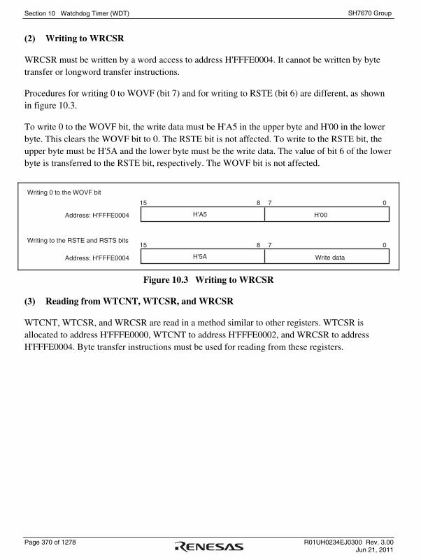
Section 10 Watchdog Timer (WDT)
Page 370 of 1278 R01UH0234EJ0300 Rev. 3.00 Jun 21, 2011
SH7670 Group
(2) Writing to WRCSR
WRCSR must be written by a word access to address H'FFFE0004. It cannot be written by byte transfer or longword transfer instructions.
Procedures for writing 0 to WOVF (bit 7) and for writing to RSTE (bit 6) are different, as shown in figure 10.3.
To write 0 to the WOVF bit, the write data must be H'A5 in the upper byte and H'00 in the lower byte. This clears the WOVF bit to 0. The RSTE bit is not affected. To write to the RSTE bit, the upper byte must be H'5A and the lower byte must be the write data. The value of bit 6 of the lower byte is transferred to the RSTE bit, respectively. The WOVF bit is not affected.
Address: H'FFFE0004
Address: H'FFFE0004
H'A5 H'00
15 8 7 0
H'5A
15 8 7 0
Writing 0 to the WOVF bit
Writing to the RSTE and RSTS bits
Write data
Figure 10.3 Writing to WRCSR
(3) Reading from WTCNT, WTCSR, and WRCSR
WTCNT, WTCSR, and WRCSR are read in a method similar to other registers. WTCSR is allocated to address H'FFFE0000, WTCNT to address H'FFFE0002, and WRCSR to address H'FFFE0004. Byte transfer instructions must be used for reading from these registers.

Section 10 Watchdog Timer (WDT)
R01UH0234EJ0300 Rev. 3.00 Page 371 of 1278 Jun 21, 2011
SH7670 Group
10.4 WDT Usage
10.4.1 Canceling Software Standby Mode
The WDT can be used to cancel software standby mode with an interrupt such as an NMI interrupt. The procedure is described below. (The WDT does not operate when resets are used for canceling, so keep the RES pin low until clock oscillation settles.)
1. Before making a transition to software standby mode, always clear the TME bit in WTCSR to 0. When the TME bit is 1, an erroneous reset or interval timer interrupt may be generated when the count overflows.
2. Set the type of count clock used in the CKS[2:0] bits in WTCSR and the initial value of the counter in WTCNT. These values should ensure that the time till count overflow is longer than the clock oscillation settling time.
3. After setting the STBY bit of the standby control register (STBCR: see section 11, Power-Down Modes) to 1, the execution of a SLEEP instruction puts the system in software standby mode and clock operation then stops.
4. The WDT starts counting by detecting the edge change of the NMI signal.
5. When the WDT count overflows, the CPG starts supplying the clock and this LSI resumes operation. The WOVF flag in WRCSR is not set when this happens.
10.4.2 Changing the Frequency
To change the frequency used by the PLL, use the WDT. When changing the frequency only by switching the divider, do not use the WDT.
1. Before changing the frequency, always clear the TME bit in WTCSR to 0. When the TME bit is 1, an erroneous reset or interval timer interrupt may be generated when the count overflows.
2. Set the type of count clock used in the CKS[2:0] bits in WTCSR and the initial value of the counter in WTCNT. These values should ensure that the time till count overflow is longer than the clock oscillation settling time. However, the WDT counts up using the clock after the setting.
3. When the frequency control register (FRQCR) is written to, this LSI stops temporarily. The WDT starts counting.
4. When the WDT count overflows, the CPG resumes supplying the clock and this LSI resumes operation. The WOVF flag in WRCSR is not set when this happens.

Section 10 Watchdog Timer (WDT)
Page 372 of 1278 R01UH0234EJ0300 Rev. 3.00 Jun 21, 2011
SH7670 Group
5. The counter stops at the value of H'00.
6. Before changing WTCNT after execution of the frequency change instruction, always confirm that the value of WTCNT is H'00 by reading from WTCNT.
10.4.3 Using Watchdog Timer Mode
1. Set the WT/IT bit in WTCSR to 1 to set the type of count clock in the CKS2 to CKS0 bits, whether this LSI is to be reset internally or not in the RSTE bit in WRCSR, and the initial value of the counter in WTCNT.
2. Set the TME bit in WTCSR to 1 to start the count in watchdog timer mode.
3. While operating in watchdog timer mode, rewrite the counter periodically to H'00 to prevent the counter from overflowing.
4. When the counter overflows, the WDT sets the WOVF flag in WRCSR to 1, and the WDTOVF signal is output externally (figure 10.4). The WDTOVF signal can be used to reset the system. The WDTOVF signal is output for 64 × Pφ clock cycles.
5. If the RSTE bit in WRCSR is set to 1, a signal to reset the inside of this LSI can be generated simultaneously with the WDTOVF signal. The internal reset signal is output for 128 × Pφ clock cycles.
6. When a WDT overflow reset is generated simultaneously with a reset input on the RES pin, the RES pin reset takes priority, and the WOVF bit in WRCSR is cleared to 0.

Section 10 Watchdog Timer (WDT)
R01UH0234EJ0300 Rev. 3.00 Page 373 of 1278 Jun 21, 2011
SH7670 Group
H'FF
H'00
Overflow
H'00 writtenin WTCNT
Internal reset signal*
WDTOVF
signal
WTCNTvalue
WDTOVF and internal reset generated
WT/IT:TME:
Timer mode select bitTimer enable bit
H'00 writtenin WTCNT
Time
128 × Pφ clock cycles
64 × Pφ clock cycles
Note: * Internal reset signal occurs only when the RSTE bit is set to 1.
[Legend]
WT/IT = 1TME = 1
WOVF = 1 WT/IT = 1TME = 1
Figure 10.4 Operation in Watchdog Timer Mode
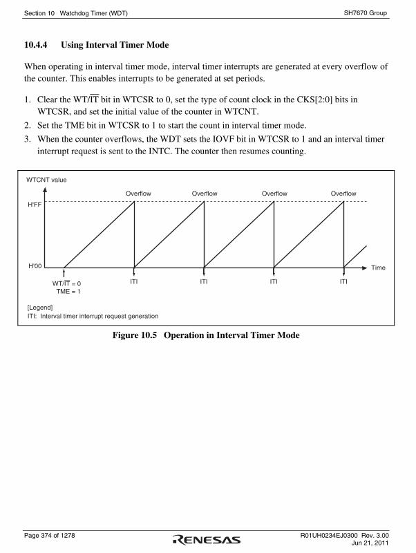
Section 10 Watchdog Timer (WDT)
Page 374 of 1278 R01UH0234EJ0300 Rev. 3.00 Jun 21, 2011
SH7670 Group
10.4.4 Using Interval Timer Mode
When operating in interval timer mode, interval timer interrupts are generated at every overflow of the counter. This enables interrupts to be generated at set periods.
1. Clear the WT/IT bit in WTCSR to 0, set the type of count clock in the CKS[2:0] bits in WTCSR, and set the initial value of the counter in WTCNT.
2. Set the TME bit in WTCSR to 1 to start the count in interval timer mode.
3. When the counter overflows, the WDT sets the IOVF bit in WTCSR to 1 and an interval timer interrupt request is sent to the INTC. The counter then resumes counting.
H'FF
ITI ITI ITI ITI
H'00
WTCNT value
ITI: Interval timer interrupt request generation
WT/IT = 0TME = 1
Time
Overflow Overflow Overflow Overflow
[Legend]
Figure 10.5 Operation in Interval Timer Mode

Section 10 Watchdog Timer (WDT)
R01UH0234EJ0300 Rev. 3.00 Page 375 of 1278 Jun 21, 2011
SH7670 Group
10.5 Usage Notes
Pay attention to the following points when using the WDT in either the interval timer or watchdog timer mode.
10.5.1 Timer Variation
After timer operation has started, the period from the power-on reset point to the first count up timing of WTCNT varies depending on the time period that is set by the TME bit of WTCSR. The shortest such time period is thus one cycle of the peripheral clock, Pφ, while the longest is the result of frequency division according to the value in the CKS[2:0] bits. The timing of subsequent incrementation is in accord with the selected frequency division ratio. Accordingly, this time difference is referred to as timer variation.
This also applies to the timing of the first incrementation after WTCNT has been written to during timer operation.
10.5.2 Prohibition against Setting H'FF to WTCNT
When the value in WTCNT reaches H'FF, the WDT assumes that an overflow has occurred. Accordingly, when H'FF is set in WTCNT, an interval timer interrupt or WDT reset will occur immediately, regardless of the current clock selection by the CKS[2:0] bits.
10.5.3 System Reset by WDTOVF Signal
If the WDTOVF signal is input to the RES pin of this LSI, this LSI cannot be initialized correctly.
Avoid input of the WDTOVF signal to the RES pin of this LSI through glue logic circuits. To reset the entire system with the WDTOVF signal, use the circuit shown in figure 10.6.
RES
WDTOVF
Reset input(Low active)
Reset signal toentire system
(Low active)
Figure 10.6 Example of System Reset Circuit Using WDTOVF Signal

Section 10 Watchdog Timer (WDT)
Page 376 of 1278 R01UH0234EJ0300 Rev. 3.00 Jun 21, 2011
SH7670 Group
10.5.4 Manual Reset in Watchdog Timer Mode
When a manual reset occurs in watchdog timer mode, the bus cycle is continued. If a manual reset occurs while the bus is released or during DMAC burst transfer, manual reset exception handling will be pended until the CPU acquires the bus mastership.
However, if the duration from generation of the manual reset to the bus cycle end is equal to or longer than the duration of the internal manual reset activated, the occurrence of the internal manual reset source is ignored instead of being pended, and the manual reset exception handling is not executed.

Section 11 Power-Down Modes
R01UH0234EJ0300 Rev. 3.00 Page 377 of 1278 Jun 21, 2011
SH7670 Group
Section 11 Power-Down Modes
In power-down modes, operation of some of the internal peripheral modules and of the CPU stops. This leads to reduced power consumption. These modes are canceled by a reset or interrupt.
11.1 Features
11.1.1 Power-Down Modes
This LSI has the following power-down modes and function:
1. Sleep mode
2. Software standby mode
3. Module standby function Table 11.1 shows the transition conditions for entering the modes from the program execution state, as well as the CPU and peripheral module states in each mode and the procedures for canceling each mode.
Table 11.1 States of Power-Down Modes
State*
Power-Down
Mode Transition Conditions CPG CPU
CPU
Register
On-Chip
Memory
On-Chip
Peripheral
Modules
External
Memory
Canceling
Procedure
Sleep mode Execute SLEEP
instruction with STBY bit
cleared to 0 in STBCR
Runs Halts Held Runs Runs Auto-
refreshing
• Interrupt
• Reset
• DMA address
error
Software
standby mode
Execute SLEEP
instruction with STBY bit
set to 1 in STBCR
Halts Halts Held Halts
(contents are
held)
Halts Self-
refreshing
• NMI interrupt
• IRQ interrupt
• Reset
Module standby
function
Set the MSTP bits in
STBCR2, STBCR3, and
STBCR4 to 1
Runs Runs Held Specified
module halts
(contents are
held)
Specified
module halts
Auto-
refreshing
• Clear MSTP bit
to 0
• Reset
Note: * The pin state is retained or set to high impedance. For details, see appendix A, Pin States.

Section 11 Power-Down Modes
Page 378 of 1278 R01UH0234EJ0300 Rev. 3.00 Jun 21, 2011
SH7670 Group
11.2 Register Descriptions
The following registers are used in power-down modes.
Table 11.2 Register Configuration
Register Name Abbreviation R/W Initial Value Address
Access Size
Standby control register STBCR R/W H'00 H'FFFE0014 8
Standby control register 2 STBCR2 R/W H'00 H'FFFE0018 8
Standby control register 3 STBCR3 R/W H'00 H'FFFE0408 8
Standby control register 4 STBCR4 R/W H'00 H'FFFE040C 8
System control register 1 SYSCR1 R/W H'FF H'FFFE0402 8
System control register 2 SYSCR2 R/W H'FF H'FFFE0404 8
System control register 3 SYSCR3 R/W H'00 H'FFFE0418 8

Section 11 Power-Down Modes
R01UH0234EJ0300 Rev. 3.00 Page 379 of 1278 Jun 21, 2011
SH7670 Group
11.2.1 Standby Control Register (STBCR)
STBCR is an 8-bit readable/writable register that specifies the state of the power-down mode. This register is initialized to H'00 by a power-on reset but retains its previous value by a manual reset or in software standby mode. Only byte access is valid.
Note: See section 11.4, Usage Notes, when writing data to this register.
7 6 5 4 3 2 1 0
0 0 0 0 0 0 0 0R/W R R R R R R R
Bit:
Initial value:R/W:
STBY ⎯ ⎯ ⎯ ⎯ ⎯ ⎯ ⎯
Bit Bit Name Initial Value R/W Description
7 STBY 0 R/W Software Standby
Specifies transition to software standby mode.
0: Executing SLEEP instruction puts chip into sleep mode.
1: Executing SLEEP instruction puts chip into software standby mode.
6 to 0 ⎯ All 0 R Reserved
These bits are always read as 0. The write value should always be 0.

Section 11 Power-Down Modes
Page 380 of 1278 R01UH0234EJ0300 Rev. 3.00 Jun 21, 2011
SH7670 Group
11.2.2 Standby Control Register 2 (STBCR2)
STBCR2 is an 8-bit readable/writable register that controls the operation of modules in power-down modes. STBCR2 is initialized to H'00 by a power-on reset but retains its previous value by a manual reset or in software standby mode. Only byte access is valid.
Note: See section 11.4, Usage Notes, when writing data to this register.
7 6 5 4 3 2 1 0Bit:
Initial Value:R/W:
0 0 0 0 0 0 0 0R/W R/W R/W R/W R R R R
MSTP10
MSTP9
MSTP8
MSTP7 ⎯ ⎯ ⎯ ⎯
Bit Bit Name Initial Value R/W Description
7 MSTP10 0 R/W Module Stop 10
When the MSTP10 bit is set to 1, the supply of the clock to the H-UDI is halted.
0: H-UDI runs.
1: Clock supply to H-UDI halted.
6 MSTP9 0 R/W Module Stop 9
When the MSTP9 bit is set to 1, the supply of the clock to the UBC is halted.
0: UBC runs.
1: Clock supply to UBC halted.
5 MSTP8 0 R/W Module Stop 8
When the MSTP8 bit is set to 1, the supply of the clock to the DMAC is halted.
0: DMAC runs.
1: Clock supply to DMAC halted.

Section 11 Power-Down Modes
R01UH0234EJ0300 Rev. 3.00 Page 381 of 1278 Jun 21, 2011
SH7670 Group
Bit Bit Name Initial Value R/W Description
4 MSTP7 0 R/W Module Stop 7
When the MSTP7 bit is set to 1, the clock supply to the FPU is halted. After the MSTP7 bit is set to 1, the value of 0 cannot be written for clearing. In other words, once the MSTP7 bit is set to 1 and the clock supply to the FPU is temporarily halted, then the clock supply to the FPU cannot be restarted by clearing the MSTP7 bit to 0.
If the clock supply to the FPU is halted and then restarted, a power-on reset must be performed for this LSI.
0: FPUC runs.
1: Clock supply to FPU halted.
3 to 0 ⎯ All 0 R Reserved
These bits are always read as 0. The write value should always be 0.

Section 11 Power-Down Modes
Page 382 of 1278 R01UH0234EJ0300 Rev. 3.00 Jun 21, 2011
SH7670 Group
11.2.3 Standby Control Register 3 (STBCR3)
STBCR3 is an 8-bit readable/writable register that controls the operation of modules in power-down modes. STBCR3 is initialized to H'00 by a power-on reset but retains its previous value by a manual reset or in software standby mode. Only byte access is valid.
Note: See section 11.4, Usage Notes, when writing data to this register.
7 6 5 4 3 2 1 0Bit:
Initial Value:R/W:
0 0 0 0 0 0 0 0R/W R/W R/W R/W R/W R/W R/W R/W
MSTP36
MSTP35
MSTP34
MSTP33
MSTP32
MSTP31HIZ MSTP
30
Bit Bit Name Initial Value R/W Description
7 HIZ 0 R/W Port High Impedance
Selects whether the state of a specified pin is retained or the pin is placed in the high-impedance state in software standby mode. See appendix A, Pin States to determine the pin to which this control is applied.
Do not set this bit when the TME bit of WTSCR of the WDT is 1. When setting the output pin to the high-impedance state, set the HIZ bit with the TME bit being 0.
0: The pin state is held in software standby mode.
1: The pin state is set to the high-impedance state in software standby mode.
6 MSTP36 0 R/W Module Stop 36
When the MSTP36 bit is set to 1, the supply of the clock to the STIF1 is halted.
0: STIF1 runs.
1: Clock supply to STIF1 halted.
5 MSTP35 0 R/W Module Stop 35
When the MSTP35 bit is set to 1, the supply of the clock to the STIF0 is halted.
0: STIF0 runs.
1: Clock supply to STIF0 halted.
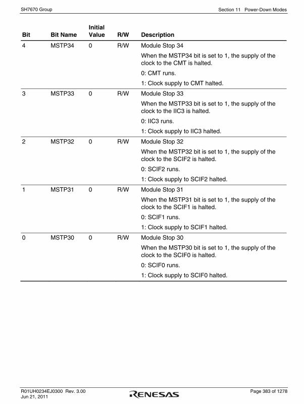
Section 11 Power-Down Modes
R01UH0234EJ0300 Rev. 3.00 Page 383 of 1278 Jun 21, 2011
SH7670 Group
Bit Bit Name Initial Value R/W Description
4 MSTP34 0 R/W Module Stop 34
When the MSTP34 bit is set to 1, the supply of the clock to the CMT is halted.
0: CMT runs.
1: Clock supply to CMT halted.
3 MSTP33 0 R/W Module Stop 33
When the MSTP33 bit is set to 1, the supply of the clock to the IIC3 is halted.
0: IIC3 runs.
1: Clock supply to IIC3 halted.
2 MSTP32 0 R/W Module Stop 32
When the MSTP32 bit is set to 1, the supply of the clock to the SCIF2 is halted.
0: SCIF2 runs.
1: Clock supply to SCIF2 halted.
1 MSTP31 0 R/W Module Stop 31
When the MSTP31 bit is set to 1, the supply of the clock to the SCIF1 is halted.
0: SCIF1 runs.
1: Clock supply to SCIF1 halted.
0 MSTP30 0 R/W Module Stop 30
When the MSTP30 bit is set to 1, the supply of the clock to the SCIF0 is halted.
0: SCIF0 runs.
1: Clock supply to SCIF0 halted.
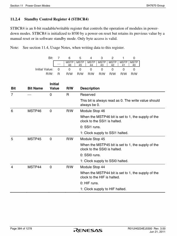
Section 11 Power-Down Modes
Page 384 of 1278 R01UH0234EJ0300 Rev. 3.00 Jun 21, 2011
SH7670 Group
11.2.4 Standby Control Register 4 (STBCR4)
STBCR4 is an 8-bit readable/writable register that controls the operation of modules in power-down modes. STBCR4 is initialized to H'00 by a power-on reset but retains its previous value by a manual reset or in software standby mode. Only byte access is valid.
Note: See section 11.4, Usage Notes, when writing data to this register.
7 6 5 4 3 2 1 0Bit:
Initial Value:R/W:
0 0 0 0 0 0R R/W R/W R/W R/W R/W
0R/W
0R/W
MSTP46⎯ MSTP
45MSTP
44MSTP
42MSTP
40MSTP
41MSTP
43
Bit Bit Name Initial Value R/W Description
7 ⎯ 0 R Reserved
This bit is always read as 0. The write value should always be 0.
6 MSTP46 0 R/W Module Stop 46
When the MSTP46 bit is set to 1, the supply of the clock to the SSI1 is halted.
0: SSI1 runs.
1: Clock supply to SSI1 halted.
5 MSTP45 0 R/W Module Stop 45
When the MSTP45 bit is set to 1, the supply of the clock to the SSI0 is halted.
0: SSI0 runs.
1: Clock supply to SSI0 halted.
4 MSTP44 0 R/W Module Stop 44
When the MSTP44 bit is set to 1, the supply of the clock to the HIF is halted.
0: HIF runs.
1: Clock supply to HIF halted.

Section 11 Power-Down Modes
R01UH0234EJ0300 Rev. 3.00 Page 385 of 1278 Jun 21, 2011
SH7670 Group
Bit Bit Name Initial Value R/W Description
3 MSTP43 0 R/W Module Stop 43
When the MSTP43 bit is set to 1, the supply of the clock to the A-DMAC is halted.
0: A-DMAC runs.
1: Clock supply to A-DMAC halted.
2 MSTP42 0 R/W Module Stop 42
When the MSTP42 bit is set to 1, the supply of the clock to the SDHI is halted.
0: SDHI runs.
1: Clock supply to SDHI halted.
1 MSTP41 0 R/W Module Stop 41
When the MSTP41 bit is set to 1, the supply of the clock to the USB is halted.
0: USB runs.
1: Clock supply to USB halted.
0 MSTP40 0 R/W Module Stop 40
When the MSTP40 bit is set to 1, the supply of the clock to the EtherC is halted.
0: EtherC runs.
1: Clock supply to EtherC halted.
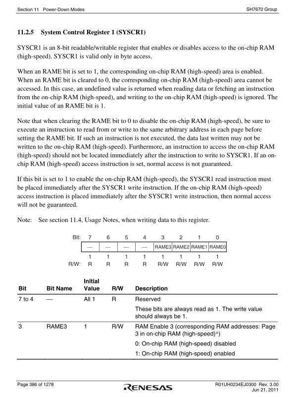
Section 11 Power-Down Modes
Page 386 of 1278 R01UH0234EJ0300 Rev. 3.00 Jun 21, 2011
SH7670 Group
11.2.5 System Control Register 1 (SYSCR1)
SYSCR1 is an 8-bit readable/writable register that enables or disables access to the on-chip RAM (high-speed). SYSCR1 is valid only in byte access.
When an RAME bit is set to 1, the corresponding on-chip RAM (high-speed) area is enabled. When an RAME bit is cleared to 0, the corresponding on-chip RAM (high-speed) area cannot be accessed. In this case, an undefined value is returned when reading data or fetching an instruction from the on-chip RAM (high-speed), and writing to the on-chip RAM (high-speed) is ignored. The initial value of an RAME bit is 1.
Note that when clearing the RAME bit to 0 to disable the on-chip RAM (high-speed), be sure to execute an instruction to read from or write to the same arbitrary address in each page before setting the RAME bit. If such an instruction is not executed, the data last written may not be written to the on-chip RAM (high-speed). Furthermore, an instruction to access the on-chip RAM (high-speed) should not be located immediately after the instruction to write to SYSCR1. If an on-chip RAM (high-speed) access instruction is set, normal access is not guaranteed.
If this bit is set to 1 to enable the on-chip RAM (high-speed), the SYSCR1 read instruction must be placed immediately after the SYSCR1 write instruction. If the on-chip RAM (high-speed) access instruction is placed immediately after the SYSCR1 write instruction, then normal access will not be guaranteed.
Note: See section 11.4, Usage Notes, when writing data to this register.
7 6 5 4 3 2 1 0Bit:
R/W:1 1 1 1 1 1 1 1R R R R R/W R/W R/W R/W
⎯ ⎯ ⎯ ⎯ RAME3 RAME2 RAME1 RAME0
Bit Bit Name Initial Value R/W Description
7 to 4 ⎯ All 1 R Reserved
These bits are always read as 1. The write value should always be 1.
3 RAME3 1 R/W RAM Enable 3 (corresponding RAM addresses: Page 3 in on-chip RAM (high-speed)*)
0: On-chip RAM (high-speed) disabled
1: On-chip RAM (high-speed) enabled

Section 11 Power-Down Modes
R01UH0234EJ0300 Rev. 3.00 Page 387 of 1278 Jun 21, 2011
SH7670 Group
Bit Bit Name Initial Value R/W Description
2 RAME2 1 R/W RAM Enable 2 (corresponding RAM addresses: Page 2 in on-chip RAM (high-speed)*)
0: On-chip RAM (high-speed) disabled
1: On-chip RAM (high-speed) enabled
1 RAME1 1 R/W RAM Enable 1 (corresponding RAM addresses: Page 1 in on-chip RAM (high-speed)*)
0: On-chip RAM (high-speed) disabled
1: On-chip RAM (high-speed) enabled
0 RAME0 1 R/W RAM Enable 0 (corresponding RAM addresses: Page 0 in on-chip RAM (high-speed)*)
0: On-chip RAM (high-speed) disabled
1: On-chip RAM (high-speed) enabled
Note: * For specific address for each page, see section 27, On-Chip RAM.
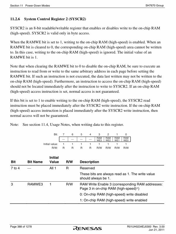
Section 11 Power-Down Modes
Page 388 of 1278 R01UH0234EJ0300 Rev. 3.00 Jun 21, 2011
SH7670 Group
11.2.6 System Control Register 2 (SYSCR2)
SYSCR2 is an 8-bit readable/writable register that enables or disables write to the on-chip RAM (high-speed). SYSCR2 is valid only in byte access.
When the RAMWE bit is set to 1, writing to the on-chip RAM (high-speed) is enabled. When an RAMWE bit is cleared to 0, the corresponding on-chip RAM (high-speed) area cannot be written to. In this case, writing to the on-chip RAM (high-speed) is ignored. The initial value of an RAMWE bit is 1.
Note that when clearing the RAMWE bit to 0 to disable the on-chip RAM, be sure to execute an instruction to read from or write to the same arbitrary address in each page before setting the RAMWE bit. If such an instruction is not executed, the data last written may not be written to the on-chip RAM (high-speed). Furthermore, an instruction to access the on-chip RAM (high-speed) should not be located immediately after the instruction to write to SYSCR2. If an on-chip RAM (high-speed) access instruction is set, normal access is not guaranteed.
If this bit is set to 1 to enable writing to the on-chip RAM (high-speed), the SYSCR2 read instruction must be placed immediately after the SYSCR2 write instruction. If the on-chip RAM (high-speed) access instruction is placed immediately after the SYSCR2 write instruction, then normal access will not be guaranteed.
Note: See section 11.4, Usage Notes, when writing data to this register.
7 6 5 4 3 2 1 0
1 1 1 1 1 1 1 1R R R R R/W R/W R/W R/W
Bit:
Initial value:R/W:
⎯ ⎯ ⎯ ⎯ RAMWE3
RAMWE2
RAMWE1
RAMWE0
Bit Bit Name Initial Value R/W Description
7 to 4 ⎯ All 1 R Reserved
These bits are always read as 1. The write value should always be 1.
3 RAMWE3 1 R/W RAM Write Enable 3 (corresponding RAM addresses: Page 3 in on-chip RAM (high-speed)*)
0: On-chip RAM (high-speed) write disabled
1: On-chip RAM (high-speed) write enabled
Section 11 Power-Down Modes
R01UH0234EJ0300 Rev. 3.00 Page 389 of 1278 Jun 21, 2011
SH7670 Group
Bit Bit Name Initial Value R/W Description
2 RAMWE2 1 R/W RAM Write Enable 2 (corresponding RAM addresses: Page 2 in on-chip RAM (high-speed)*)
0: On-chip RAM (high-speed) write disabled
1: On-chip RAM (high-speed) write enabled
1 RAMWE1 1 R/W RAM Write Enable 1 (corresponding RAM addresses: Page 1 in on-chip RAM (high-speed)*)
0: On-chip RAM (high-speed) write disabled
1: On-chip RAM (high-speed) write enabled
0 RAMWE0 1 R/W RAM Write Enable 0 (corresponding RAM addresses: Page 0 in on-chip RAM (high-speed)*)
0: On-chip RAM (high-speed) write disabled
1: On-chip RAM (high-speed) write enabled
Note: * For specific address for each page, see section 27, On-Chip RAM.

Section 11 Power-Down Modes
Page 390 of 1278 R01UH0234EJ0300 Rev. 3.00 Jun 21, 2011
SH7670 Group
11.2.7 System Control Register 3 (SYSCR3)
SYSCR3 is an 8-bit readable/writable register that controls the software reset for SSI0 and SSI1. SYSCR3 is valid only in byte access.
Note: See section 11.4, Usage Notes, when writing data to this register.
7 6 5 4 3 2 1 0Bit:
Initial value:R/W:
0 0 0 0 0 0 0 0R R R R R R R/W R/W
⎯ ⎯ ⎯ ⎯ ⎯ ⎯ SSI0SRST
SSI1SRST
Bit Bit Name Initial Value R/W Description
7 to 2 ⎯ All 0 R Reserved
These bits are always read as 0. The write value should always be 0.
1 SSI1SRST 0 R/W SSI1 Software Reset
Controls the SSI1 reset by software.
0: Cancels the SSI1 reset.
1: Places the SSI1 in reset state.
0 SSI0SRST 0 R/W SSI0 Software Reset
Controls the SSI0 reset by software.
0: Cancels the SSI0 reset
1: Places the SSI0 in reset state.

Section 11 Power-Down Modes
R01UH0234EJ0300 Rev. 3.00 Page 391 of 1278 Jun 21, 2011
SH7670 Group
11.3 Operation
11.3.1 Sleep Mode
(1) Transition to Sleep Mode
Executing the SLEEP instruction when the STBY bit in STBCR is 0 causes a transition from the program execution state to sleep mode. Although the CPU halts immediately after executing the SLEEP instruction, the contents of its internal registers remain unchanged. The on-chip modules continue to run in sleep mode. Clock pulses continue to be output on the CKIO pin in clock mode 0, 1, or 3.
(2) Canceling Sleep Mode
Sleep mode is canceled by an interrupt (NMI, IRQ, and on-chip peripheral module), DMA address error, or reset (power-on reset).
• Canceling with an interrupt
When an NMI, IRQ, or on-chip peripheral module interrupt occurs, sleep mode is canceled and interrupt exception handling is executed. When the priority level of the generated interrupt is equal to or lower than the interrupt mask level that is set in the status register (SR) of the CPU, or the interrupt by the on-chip peripheral module is disabled on the module side, the interrupt request is not accepted and sleep mode is not canceled.
• Canceling with a DMA address error
When a DMA address error occurs, sleep mode is canceled and DMA address error exception handling is executed.
• Canceling with a reset
Sleep mode is canceled by a power-on reset.

Section 11 Power-Down Modes
Page 392 of 1278 R01UH0234EJ0300 Rev. 3.00 Jun 21, 2011
SH7670 Group
11.3.2 Software Standby Mode
(1) Transition to Software Standby Mode
The LSI switches from a program execution state to software standby mode by executing the SLEEP instruction when the STBY bit in STBCR is 1. In software standby mode, not only the CPU but also the clock and on-chip peripheral modules halt. The clock output from the CKIO pin also halts in clock mode 0, 1, or 3.
The contents of the CPU remain unchanged. Some registers of on-chip peripheral modules are, however, initialized. Regarding the states of on-chip peripheral module registers in software standby mode, see section 28.3, Register States in Each Operating Mode.
The CPU takes one cycle to finish writing to STBCR, and then executes processing for the next instruction. However, it takes one or more cycles to actually write. Therefore, execute a SLEEP instruction after reading STBCR to have the values written to STBCR by the CPU to be definitely reflected in the SLEEP instruction.
The procedure for switching to software standby mode is as follows:
1. Clear the TME bit in the WDT's timer control register (WTCSR) to 0 to stop the WDT.
2. Set the WDT's timer counter (WTCNT) to 0 and the CKS[2:0] bits in WTCSR to appropriate values to secure the specified oscillation settling time.
3. After setting the STBY bit in STBCR to 1, read STBCR. Then, execute a SLEEP instruction.

Section 11 Power-Down Modes
R01UH0234EJ0300 Rev. 3.00 Page 393 of 1278 Jun 21, 2011
SH7670 Group
(2) Canceling Software Standby Mode
Software standby mode is canceled by interrupts (NMI or IRQ) or a reset (power-on reset). The CKIO pin starts outputting the clock in clock mode 0, 1, or 3.
• Canceling with an interrupt
When the falling edge or rising edge of the NMI pin (selected by the NMI edge select bit (NMIE) in interrupt control register 0 (ICR0) of the interrupt controller (INTC)) or the falling edge or rising edge of an IRQ pin (IRQ7 to IRQ0) (selected by the IRQn sense select bits (IRQn1S and IRQn0S) in interrupt control register 1 (ICR1) of the interrupt controller (INTC)) is detected, clock oscillation is started. This clock pulse is supplied only to the oscillation settling counter (WDT) used to count the oscillation settling time.
After the elapse of the time set in the clock select bits (CKS[2:0]) in the watchdog timer control/status register (WTCSR) of the WDT before the transition to software standby mode, the WDT overflow occurs. Since this overflow indicates that the clock has been stabilized, the clock pulse will be supplied to the entire chip after this overflow. Software standby mode is thus cleared and NMI interrupt exception handling (IRQ interrupt exception handling in the case of IRQ) starts. However, if the priority level of IRQ interrupt is lower than the interrupt mask level set in the status register (SR) of the CPU, the interrupt request is not accepted and thus the software standby mode is not released.
When canceling software standby mode by the NMI interrupt or IRQ interrupt, set the CKS[2:0] bits so that the WDT overflow period will be equal to or longer than the oscillation settling time.
The clock output phase of the CKIO pin may be unstable immediately after detecting an interrupt and until software standby mode is canceled. When software standby mode is canceled by the falling edge of the NMI pin, the NMI pin should be high when the CPU enters software standby mode (when the clock pulse stops) and should be low when the CPU returns from software standby mode (when the clock is initiated after the oscillation settling). When software standby mode is canceled by the rising edge of the NMI pin, the NMI pin should be low when the CPU enters software standby mode (when the clock pulse stops) and should be high when the CPU returns from software standby mode (when the clock is initiated after the oscillation settling) (This is the same with the IRQ pin.)
• Canceling with a reset
When the RES pin is driven low, software standby mode is released and this LSI enters the power-on reset state. And if the RES pin is driven high after that, the power-on reset exception handling starts.
Keep the RES pin low until the clock oscillation settles.

Section 11 Power-Down Modes
Page 394 of 1278 R01UH0234EJ0300 Rev. 3.00 Jun 21, 2011
SH7670 Group
11.3.3 Software Standby Mode Application Example
This example describes a transition to software standby mode on the falling edge of the NMI signal, and cancellation on the rising edge of the NMI signal. The timing is shown in figure 11.1.
When the NMI pin is changed from high to low level while the NMI edge select bit (NMIE) in ICR is set to 0 (falling edge detection), the NMI interrupt is accepted. When the NMIE bit is set to 1 (rising edge detection) by the NMI exception service routine, the STBY bit in STBCR is set to 1, and a SLEEP instruction is executed, software standby mode is entered. Thereafter, software standby mode is canceled when the NMI pin is changed from low to high level.
CK
NMI pin
NMIE bit
STBY bit
LSI state
Oscillator
Programexecution
NMIexceptionhandling
NMI exceptionhandling
Exceptionservice routine
Softwarestandby mode
Oscillationsettling time
Figure 11.1 NMI Timing in Software Standby Mode (Application Example)

Section 11 Power-Down Modes
R01UH0234EJ0300 Rev. 3.00 Page 395 of 1278 Jun 21, 2011
SH7670 Group
11.3.4 Module Standby Function
(1) Transition to Module Standby Function
Setting the standby control register MSTP bits to 1 halts the supply of clocks to the corresponding on-chip peripheral modules. This function can be used to reduce the power consumption in normal mode and sleep mode. Disable a module before placing it in the module standby mode. In addition, do not access the module's registers while it is in the module standby state.
The register states are the same as those in software standby mode. For details, see section 28.3, Register States in Each Operating Mode.
However, the states of the CMT registers are exceptional. In the CMT, all registers are initialized in software standby mode, but retain their previous values in module standby mode.
(2) Canceling Module Standby Function
The module standby function can be canceled by clearing the MSTP bits to 0, or by a power-on reset. When taking a module out of the module standby state by clearing the corresponding MSTP bit to 0, read the MSTP bit to confirm that it has been cleared to 0.

Section 11 Power-Down Modes
Page 396 of 1278 R01UH0234EJ0300 Rev. 3.00 Jun 21, 2011
SH7670 Group
11.4 Usage Notes
When writing data to registers related to power-down modes, note the following suggestion.
In a case where the CPU writes data to the registers related to power-down modes, if the CPU once starts executing the write instruction, the CPU keeps on executing the succeeding instructions without waiting for the completion of writing data to the registers. If reflecting a change of writing data to registers becomes necessary while the CPU is performing the succeeding instructions, execute a dummy read for the same register between the write instruction to the register and the succeeding instructions.
Section 12 Ethernet Controller (EtherC)
R01UH0234EJ0300 Rev. 3.00 Page 397 of 1278 Jun 21, 2011
SH7670 Group
Section 12 Ethernet Controller (EtherC)
This LSI has an on-chip Ethernet controller (EtherC) conforming to the Ethernet or the IEEE802.3 MAC (Media Access Control) layer standard. Connecting a physical-layer LSI (PHY-LSI) complying with this standard enables the Ethernet controller (EtherC) to perform transmission and reception of Ethernet/IEEE802.3 frames. This LSI has one MAC layer interface.
The Ethernet controller is connected to the direct memory access controller for Ethernet controller (E-DMAC) inside this LSI, and carries out high-speed data transfer to and from the memory.
Figure 12.1 shows a configuration of the EtherC.
12.1 Features
• Transmission and reception of Ethernet/IEEE802.3 frames
• Supports 10/100 Mbps receive/transfer
• Supports full-duplex and half-duplex modes
• Conforms to IEEE802.3u standard MII (Media Independent Interface)
• Magic Packet detection and Wake-On-LAN (WOL) signal output
• Conforms to IEEE802.3x flow control

Section 12 Ethernet Controller (EtherC)
Page 398 of 1278 R01UH0234EJ0300 Rev. 3.00 Jun 21, 2011
SH7670 Group
MAC
EtherC
PHY
E-DMAC
E-DMAC interface
Receive controller
Transmit controller
Command statusinterface
MII
Figure 12.1 Configuration of EtherC

Section 12 Ethernet Controller (EtherC)
R01UH0234EJ0300 Rev. 3.00 Page 399 of 1278 Jun 21, 2011
SH7670 Group
12.2 Input/Output Pins
Table 12.1 lists the pin configuration of the EtherC.
Table 12.1 Pin Configuration
Port Abbreviation I/O Function
0 TX-CLK* Input Transmit Clock
Timing reference signal for the TX-EN, MII_TXD3 to MII_TXD0, TX-ER signals
0 RX-CLK* Input Receive Clock
Timing reference signal for the RX-DV, MII_RXD3 to MII_RXD0, RX-ER signals
0 TX-EN* Output Transmit Enable
Indicates that transmit data is ready on pins MII_TXD3 to MII_TXD0.
0 MII_TXD3 to MII_TXD0*
Output Transmit Data
4-bit transmit data
0 TX-ER* Output Transmit Error
Notifies the PHY-LSI of error during transmission
0 RX-DV* Input Receive Data Valid
Indicates that valid receive data is on pins MII_RXD3 to MII_RXD0.
0 MII_RXD3 to MII_RXD0*
Input Receive Data
4-bit receive data
0 RX-ER* Input Receive Error
Identifies error state occurred during data reception.
0 CRS Input Carrier Detection
Carrier detection signal
0 COL Input Collision Detection
Collision detection signal
0 MDC Output Management Data Clock
Reference clock signal for information transfer via MDIO
0 MDIO Input/ Output
Management Data I/O
Bidirectional signal for exchange of management information between this LSI and PHY

Section 12 Ethernet Controller (EtherC)
Page 400 of 1278 R01UH0234EJ0300 Rev. 3.00 Jun 21, 2011
SH7670 Group
Port Abbreviation I/O Function
0 LNKSTA Input Link Status
Inputs link status from PHY
0 EXOUT Output General-Purpose External Output
Signal indicating value of register-bit (ECMR0-ELB)
0 WOL Output Wake-On-LAN
Signal indicating reception of Magic Packet
Note: * MII signal conforming to IEEE802.3u

Section 12 Ethernet Controller (EtherC)
R01UH0234EJ0300 Rev. 3.00 Page 401 of 1278 Jun 21, 2011
SH7670 Group
12.3 Register Description
The EtherC has the following registers. For details on addresses and access sizes of registers, see section 28, List of Registers.
MAC Layer Interface Control Registers:
• EtherC mode register (ECMR)
• EtherC status register (ECSR)
• EtherC interrupt permission register (ECSIPR)
• PHY interface register (PIR)
• MAC address high register (MAHR)
• MAC address low register (MALR)
• Receive frame length register (RFLR)
• PHY status register (PSR)
• Transmit retry over counter register (TROCR)
• Delayed collision detect counter register (CDCR)
• Lost carrier counter register (LCCR)
• Carrier not detect counter register (CNDCR)
• CRC error frame counter register (CEFCR)
• Frame receive error counter register (FRECR)
• Too-short frame receive counter register (TSFRCR)
• Too-long frame receive counter register (TLFRCR)
• Residual-bit frame counter register (RFCR)
• Multicast address frame counter register (MAFCR)
• IPG register (IPGR)
• Automatic PAUSE frame set register (APR)
• Manual PAUSE frame set register (MPR)
• PAUSE frame retransfer count set register (TPAUSER)

Section 12 Ethernet Controller (EtherC)
Page 402 of 1278 R01UH0234EJ0300 Rev. 3.00 Jun 21, 2011
SH7670 Group
12.3.1 EtherC Mode Register (ECMR)
ECMR is a 32-bit readable/writable register and specifies the operating mode of the Ethernet controller. The settings in this register are normally made in the initialization process following a reset.
The operating mode setting must not be changed while the transmitting and receiving functions are enabled. To switch the operating mode, return the EtherC and E-DMAC to their initial states by means of the SWR bit in EDMR before making settings again.
31 30 29 28 27 26 25 24 23 22 21 20 19 18 17 16Bit:
Initial value:
R/W:
15 14 13 12 11 10 9 8 7 6 5 4 3 2 1 0Bit:
Initial value:
R/W:
0 0 0 0 0 0 0 0 0 0 0 0 0 0 0 0
R R R R R R R R R R R R R/W R/W R/W R/W
0 0 0 0 0 0 0 0 0 0 0 0 0 0 0 0
R R R R/W R R R/W R R R/W R/W R R/W R/W R/W R/W
- - - - - - - - - - - - ZPF PFR RXF TXF
- - - PRCEF - - MPDE - - RE TE - ILB ELB DM PRM
Bit Bit NameInitial Value R/W Description
31 to 20 ⎯ All 0 R Reserved
These bits are always read as 0. The write value should always be 0.
19 ZPF 0 R/W 0 time parameter PAUSE Frame Use Enable
0: Disables PAUSE frame control in which the TIME parameter is 0.
The next frame is transmitted after the time indicated by the Timer value has elapsed. When the EtherC receives a PAUSE frame with the time indicated by the Timer value set to 0, the PAUSE frame is discarded.
1: Enables PAUSE frame control in which the TIME parameter is 0.
A PAUSE frame with the Timer value set to 0 is transmitted when the number of data in the receive FIFO is less than the FCFTR value before the time indicated by the Timer value has not elapsed. When the EtherC receives a PAUSE frame with the time indicated by the Timer value set to 0, the transmit wait state is canceled.

Section 12 Ethernet Controller (EtherC)
R01UH0234EJ0300 Rev. 3.00 Page 403 of 1278 Jun 21, 2011
SH7670 Group
Bit Bit Name Initial Value R/W Description
18 PFR 0 R/W PAUSE Frame Receive Mode
0: PAUSE frame is not transferred to the E-DMAC
1: PAUSE frame is transferred to the E-DMAC
17 RXF 0 R/W Receive Flow Control Operating Mode
0: PAUSE frame detection function is disabled
1: Receive flow control function is enabled
16 TXF 0 R/W Transmit Flow Control Operating mode
0: Transmit flow control function is disabled
1: Transmit flow control function is enabled
15 to 13 ⎯ All 0 R Reserved
These bits are always read as 0. The write value should always be 0.
12 PRCEF 0 R/W Permit Receive CRC Error Frame
0: A frame with a CRC error is received as a frame with an error.
1: A frame with a CRC error is received as a frame without an error.
For a frame with an error, a CRC error is reflected in the ECSR of the E-DMAC and the status of the receive descriptor. For a frame without an error, the frame is received as normal frame.
11, 10 ⎯ All 0 R Reserved
These bits are always read as 0. The write value should always be 0.
9 MPDE 0 R/W Magic Packet Detection Enable
Enables or disables Magic Packet detection by hardware to allow activation from the Ethernet.
0: Magic Packet detection is not enabled
1: Magic Packet detection is enabled
8, 7 ⎯ All 0 R Reserved
These bits are always read as 0. The write value should always be 0.
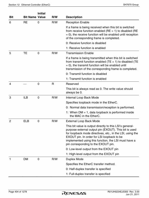
Section 12 Ethernet Controller (EtherC)
Page 404 of 1278 R01UH0234EJ0300 Rev. 3.00 Jun 21, 2011
SH7670 Group
Bit Bit NameInitial Value R/W Description
6 RE 0 R/W Reception Enable
If a frame is being received when this bit is switched from receive function enabled (RE = 1) to disabled (RE = 0), the receive function will be enabled until reception of the corresponding frame is completed.
0: Receive function is disabled
1: Receive function is enabled
5 TE 0 R/W Transmission Enable
If a frame is being transmitted when this bit is switched from transmit function enabled (TE = 1) to disabled (TE = 0), the transmit function will be enabled until transmission of the corresponding frame is completed.
0: Transmit function is disabled
1: Transmit function is enabled
4 ⎯ 0 R Reserved
This bit is always read as 0. The write value should always be 0.
3 ILB 0 R/W Internal Loop Back Mode
Specifies loopback mode in the EtherC.
0: Normal data transmission/reception is performed.
1: When DM = 1, data loopback is performed inside the MAC in the EtherC.
2 ELB 0 R/W External Loop Back Mode
This bit value is output directly to this LSI’s general-purpose external output pin (EXOUT). This bit is used for loopback mode directives, etc., in the LSI, using the EXOUT pin. In order for LSI loopback to be implemented using this function, the LSI must have a pin corresponding to the EXOUT pin.
0: Low-level output from the EXOUT pin
1: High-level output from the EXOUT pin
1 DM 0 R/W Duplex Mode
Specifies the EtherC transfer method.
0: Half-duplex transfer is specified
1: Full-duplex transfer is specified

Section 12 Ethernet Controller (EtherC)
R01UH0234EJ0300 Rev. 3.00 Page 405 of 1278 Jun 21, 2011
SH7670 Group
Bit Bit Name Initial Value R/W Description
0 PRM 0 R/W Promiscuous Mode
Setting this bit enables all Ethernet frames to be received. All Ethernet frames means all receivable frames, irrespective of differences or enabled/disabled status (destination address, broadcast address, multicast bit, etc.).
0: EtherC performs normal operation
1: EtherC performs promiscuous mode operation
12.3.2 EtherC Status Register (ECSR)
ECSR is a 32-bit readable/writable register and indicates the status in the EtherC. This status can be notified to the CPU by interrupts. When 1 is written to the PSRTO, LCHNG, MPD, and ICD, the corresponding flags can be cleared. Writing 0 does not affect the flag. For bits that generate interrupt, the interrupt can be enabled or disabled according to the corresponding bit in ECSIPR.
The interrupts generated due to this status register are indicated in the ECI bit in EESR.
31 30 29 28 27 26 25 24 23 22 21 20 19 18 17 16Initial value:
Initial value:
R/W:
15 14 13 12 11 10 9 8 7 6 5 4 3 2 1 0Bit:
Initial value:
R/W:
0 0 0 0 0 0 0 0 0 0 0 0 0 0 0 0
R R R R R R R R R R R R R R R R
0 0 0 0 0 0 0 0 0 0 0 0 0 0 0 0
R R R R R R R R R R R R/W R R/W R/W R/W
- - - - - - - - - - - - - - - -
- - - - - - - - - - - PSRTO - LCHNG MPD ICD
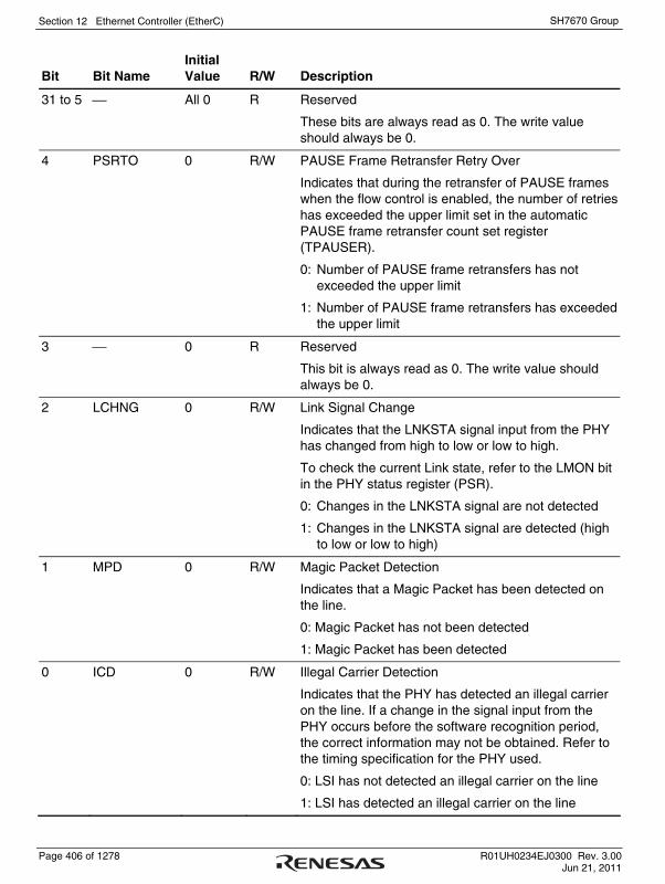
Section 12 Ethernet Controller (EtherC)
Page 406 of 1278 R01UH0234EJ0300 Rev. 3.00 Jun 21, 2011
SH7670 Group
Bit Bit Name Initial Value R/W Description
31 to 5 ⎯ All 0 R Reserved
These bits are always read as 0. The write value should always be 0.
4 PSRTO 0 R/W PAUSE Frame Retransfer Retry Over
Indicates that during the retransfer of PAUSE frames when the flow control is enabled, the number of retries has exceeded the upper limit set in the automatic PAUSE frame retransfer count set register (TPAUSER).
0: Number of PAUSE frame retransfers has not exceeded the upper limit
1: Number of PAUSE frame retransfers has exceeded the upper limit
3 ⎯ 0 R Reserved
This bit is always read as 0. The write value should always be 0.
2 LCHNG 0 R/W Link Signal Change
Indicates that the LNKSTA signal input from the PHY has changed from high to low or low to high.
To check the current Link state, refer to the LMON bit in the PHY status register (PSR).
0: Changes in the LNKSTA signal are not detected
1: Changes in the LNKSTA signal are detected (high to low or low to high)
1 MPD 0 R/W Magic Packet Detection
Indicates that a Magic Packet has been detected on the line.
0: Magic Packet has not been detected
1: Magic Packet has been detected
0 ICD 0 R/W Illegal Carrier Detection
Indicates that the PHY has detected an illegal carrier on the line. If a change in the signal input from the PHY occurs before the software recognition period, the correct information may not be obtained. Refer to the timing specification for the PHY used.
0: LSI has not detected an illegal carrier on the line
1: LSI has detected an illegal carrier on the line
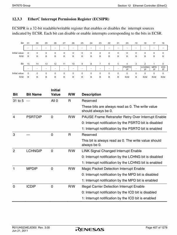
Section 12 Ethernet Controller (EtherC)
R01UH0234EJ0300 Rev. 3.00 Page 407 of 1278 Jun 21, 2011
SH7670 Group
12.3.3 EtherC Interrupt Permission Register (ECSIPR)
ECSIPR is a 32-bit readable/writable register that enables or disables the interrupt sources indicated by ECSR. Each bit can disable or enable interrupts corresponding to the bits in ECSR.
31 30 29 28 27 26 25 24 23 22 21 20 19 18 17 16Bit:
Initial value:
R/W:
15 14 13 12 11 10 9 8 7 6 5 4 3 2 1 0Bit:
Initial value:
R/W:
0 0 0 0 0 0 0 0 0 0 0 0 0 0 0 0
R R R R R R R R R R R R R R R R
0 0 0 0 0 0 0 0 0 0 0 0 0 0 0 0
R R R R R R R R R R R R/W R R/W R/W R/W
- - - - - - - - - - - - - - - -
- - - - - - - - - - - PSRTOIP - LCHNG
IPMPD
IPICDIP
Bit Bit Name Initial Value R/W Description
31 to 5 ⎯ All 0 R Reserved
These bits are always read as 0. The write value should always be 0.
4 PSRTOIP 0 R/W PAUSE Frame Retransfer Retry Over Interrupt Enable
0: Interrupt notification by the PSRTO bit is disabled
1: Interrupt notification by the PSRTO bit is enabled
3 — 0 R Reserved
This bit is always read as 0. The write value should always be 0.
2 LCHNGIP 0 R/W LINK Signal Changed Interrupt Enable
0: Interrupt notification by the LCHNG bit is disabled
1: Interrupt notification by the LCHNG bit is enabled
1 MPDIP 0 R/W Magic Packet Detection Interrupt Enable
0: Interrupt notification by the MPD bit is disabled
1: Interrupt notification by the MPD bit is enabled
0 ICDIP 0 R/W Illegal Carrier Detection Interrupt Enable
0: Interrupt notification by the ICD bit is disabled
1: Interrupt notification by the ICD bit is enabled

Section 12 Ethernet Controller (EtherC)
Page 408 of 1278 R01UH0234EJ0300 Rev. 3.00 Jun 21, 2011
SH7670 Group
12.3.4 PHY Interface Register (PIR)
PIR is a 32-bit readable/writable register that provides a means of accessing the PHY registers via the MII.
31 30 29 28 27 26 25 24 23 22 21 20 19 18 17 16Bit:
Initial value:R/W:
15 14 13 12 11 10 9 8 7 6 5 4 3 2 1 0Bit:
Initial value:R/W:
0 0 0 0 0 0 0 0 0 0 0 0 0 0 0 0R R R R R R R R R R R R R R R R
0 0 0 0 0 0 0 0 0 0 0 0 Undefined 0 0 0R R R R R R R R R R R R R R/W R/W R/W
- - - - - - - - - - - - - - - -
- - - - - - - - - - - - MDI MDO MMD MDC
Bit Bit Name Initial Value R/W Description
31 to 4 ⎯ All 0 R Reserved
These bits are always read as 0. The write value should always be 0.
3 MDI Undefined R MII Management Data-In
Indicates the level of the MDIO pin.
2 MDO 0 R/W MII Management Data-Out
Outputs the value set to this bit from the MDIO pin, when the MMD bit is 1.
1 MMD 0 R/W MII Management Mode
Specifies the data read/write direction with respect to the MII.
0: Read direction is indicated
1: Write direction is indicated
0 MDC 0 R/W MII Management Data Clock
Outputs the value set to this bit from the MDC pin and supplies the MII with the management data clock. For the method of accessing the MII registers, see section 12.4.4, Accessing MII Registers.

Section 12 Ethernet Controller (EtherC)
R01UH0234EJ0300 Rev. 3.00 Page 409 of 1278 Jun 21, 2011
SH7670 Group
12.3.5 MAC Address High Register (MAHR)
MAHR is a 32 -bit readable/writable register that specifies the upper 32 bits of the 48-bit MAC address. The settings in this register are normally made in the initialization process after a reset. The MAC address setting must not be changed while the transmitting and receiving functions are enabled. To switch the MAC address setting, return the EtherC and E-DMAC to their initial states by means of the SWR bit in EDMR before making settings again.
31 30 29 28 27 26 25 24 23 22 21 20 19 18 17 16Bit:
Initial value:R/W:
15 14 13 12 11 10 9 8 7 6 5 4 3 2 1 0Bit:
Initial value:R/W:
0 0 0 0 0 0 0 0 0 0 0 0 0 0 0 0R/W R/W R/W R/W R/W R/W R/W R/W R/W R/W R/W R/W R/W R/W R/W R/W
0 0 0 0 0 0 0 0 0 0 0 0 0 0 0 0R/W R/W R/W R/W R/W R/W R/W R/W R/W R/W R/W R/W R/W R/W R/W R/W
MA[47:32]
MA[31:16]
Bit Bit Name Initial Value R/W Description
31 to 0 MA[47:16] All 0 R/W MAC Address Bits
These bits are used to set the upper 32 bits of the MAC address.
If the MAC address is 01-23-45-67-89-AB (hexadecimal), the value set in this register is H'01234567.

Section 12 Ethernet Controller (EtherC)
Page 410 of 1278 R01UH0234EJ0300 Rev. 3.00 Jun 21, 2011
SH7670 Group
12.3.6 MAC Address Low Register (MALR)
MALR is a 32-bit readable/writable register that specifies the lower 16 bits of the 48-bit MAC address. The settings in this register are normally made in the initialization process after a reset. The MAC address setting must not be changed while the transmitting and receiving functions are enabled. To switch the MAC address setting, return the EtherC and E-DMAC to their initial states by means of the SWR bit in EDMR before making settings again.
31 30 29 28 27 26 25 24 23 22 21 20 19 18 17 16Bit:
Initial value:R/W:
15 14 13 12 11 10 9 8 7 6 5 4 3 2 1 0Bit:
Initial value:R/W:
0 0 0 0 0 0 0 0 0 0 0 0 0 0 0 0R R R R R R R R R R R R R R R R
0 0 0 0 0 0 0 0 0 0 0 0 0 0 0 0R/W R/W R/W R/W R/W R/W R/W R/W R/W R/W R/W R/W R/W R/W R/W R/W
- - - - - - - - - - - - - - - -
MA[15:0]
Bit Bit Name Initial Value R/W Description
31 to 16 ⎯ All 0 R Reserved
These bits are always read as 0. The write value should always be 0.
15 to 0 MA[15:0] All 0 R/W MAC Address Bits 15 to 0
These bits are used to set the lower 16 bits of the MAC address.
If the MAC address is 01-23-45-67-89-AB (hexadecimal), the value set in this register is H'000089AB.

Section 12 Ethernet Controller (EtherC)
R01UH0234EJ0300 Rev. 3.00 Page 411 of 1278 Jun 21, 2011
SH7670 Group
12.3.7 Receive Frame Length Register (RFLR)
RFLR is a 32-bit readable/writable register and it specifies the maximum frame length (in bytes) that can be received by this LSI. The settings in this register must not be changed while the receiving function is enabled.
31 30 29 28 27 26 25 24 23 22 21 20 19 18 17 16Bit:
Initial value:R/W:
15 14 13 12 11 10 9 8 7 6 5 4 3 2 1 0bit:
Initial value:R/W:
0 0 0 0 0 0 0 0 0 0 0 0 0 0 0 0R R R R R R R R R R R R R R R R
0 0 0 0 0 0 0 0 0 0 0 0 0 0 0 0R R R R R/W R/W R/W R/W R/W R/W R/W R/W R/W R/W R/W R/W
- - - -
- - - -
- - - - - - - - - - - -
RFL[11:0]
Bit Bit Name Initial Value R/W Description
31 to 12 ⎯ All 0 R Reserved
These bits are always read as 0. The write value should always be 0.
11 to 0 RFL[11:0] All 0 R/W Receive Frame Length 11 to 0
The frame length described here refers to all fields from the destination address up to and including the CRC data. Frame contents from the destination address up to and including the data are actually transferred to memory. CRC data is not included in the transfer.
When data that exceeds the specified value is received, the part of the data that exceeds the specified value is discarded.
H'000 to H'5EE: 1,518 bytes
H'5EF: 1,519 bytes
H'5F0: 1,520 bytes
:
:
H'7FF: 2,047 bytes
H'800 to H'FFF: 2,048 bytes

Section 12 Ethernet Controller (EtherC)
Page 412 of 1278 R01UH0234EJ0300 Rev. 3.00 Jun 21, 2011
SH7670 Group
12.3.8 PHY Status Register (PSR)
PSR is a read-only register that can read interface signals from the PHY.
31 30 29 28 27 26 25 24 23 22 21 20 19 18 17 16Bit:
Initial value:R/W:
15 14 13 12 11 10 9 8 7 6 5 4 3 2 1 0Bit:
Initial value:R/W:
0 0 0 0 0 0 0 0 0 0 0 0 0 0 0 0R R R R R R R R R R R R R R R R
0 0 0 0 0 0 0 0 0 0 0 0 0 0 0 undefined
R R R R R R R R R R R R R R R R
- - - - - - - - - - - - - - - -
- - - - - - - - - - - - - - - LMON
Bit Bit Name Initial Value R/W Description
31 to 1 ⎯ All 0 R Reserved
These bits are always read as 0. The write value should always be 0.
0 LMON 0 R LNKSTA Pin Status
The Link status can be read by connecting the Link signal output from the PHY to the LNKSTA pin. For the polarity, refer to the PHY specifications to be connected.
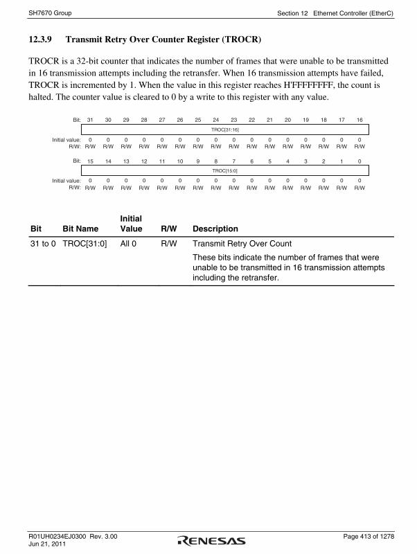
Section 12 Ethernet Controller (EtherC)
R01UH0234EJ0300 Rev. 3.00 Page 413 of 1278 Jun 21, 2011
SH7670 Group
12.3.9 Transmit Retry Over Counter Register (TROCR)
TROCR is a 32-bit counter that indicates the number of frames that were unable to be transmitted in 16 transmission attempts including the retransfer. When 16 transmission attempts have failed, TROCR is incremented by 1. When the value in this register reaches H'FFFFFFFF, the count is halted. The counter value is cleared to 0 by a write to this register with any value.
31 30 29 28 27 26 25 24 23 22 21 20 19 18 17 16
15 14 13 12 11 10 9 8 7 6 5 4 3 2 1 0
0 0 0 0 0 0 0 0 0 0 0 0 0 0 0 0R/W R/W R/W R/W R/W R/W R/W R/W R/W R/W R/W R/W R/W R/W R/W R/W
0 0 0 0 0 0 0 0 0 0 0 0 0 0 0 0R/W R/W R/W R/W R/W R/W R/W R/W R/W R/W R/W R/W R/W R/W R/W R/W
TROC[31:16]
TROC[15:0]
Bit:
Initial value:R/W:
Bit:
Initial value:R/W:
Bit Bit Name Initial Value R/W Description
31 to 0 TROC[31:0] All 0 R/W Transmit Retry Over Count
These bits indicate the number of frames that were unable to be transmitted in 16 transmission attempts including the retransfer.

Section 12 Ethernet Controller (EtherC)
Page 414 of 1278 R01UH0234EJ0300 Rev. 3.00 Jun 21, 2011
SH7670 Group
12.3.10 Delayed Collision Detect Counter Register (CDCR)
CDCR is a 32-bit counter that indicates the number of delayed collisions on all lines from a start of transmission. When the value in this register reaches H'FFFFFFFF, count-up is halted. The counter value is cleared to 0 by a write to this register with any value.
31 30 29 28 27 26 25 24 23 22 21 20 19 18 17 16Bit:
Initial value:R/W:
15 14 13 12 11 10 9 8 7 6 5 4 3 2 1 0Bit:
Initial value:R/W:
0 0 0 0 0 0 0 0 0 0 0 0 0 0 0 0R/W R/W R/W R/W R/W R/W R/W R/W R/W R/W R/W R/W R/W R/W R/W R/W
0 0 0 0 0 0 0 0 0 0 0 0 0 0 0 0R/W R/W R/W R/W R/W R/W R/W R/W R/W R/W R/W R/W R/W R/W R/W R/W
COSDC[31:16]
COSDC[15:0]
Bit Bit Name Initial Value R/W Description
31 to 0 COSDC[31:0] All 0 R/W Delayed Collision Detect Count
These bits indicate the number of delayed collisions on all lines from a start of transmission.

Section 12 Ethernet Controller (EtherC)
R01UH0234EJ0300 Rev. 3.00 Page 415 of 1278 Jun 21, 2011
SH7670 Group
12.3.11 Lost Carrier Counter Register (LCCR)
LCCR is a 32-bit counter that indicates the number of times the carrier was lost during data transmission. When the value in this register reaches H'FFFFFFFF, the count is halted. The counter value is cleared to 0 by writing to this register with any value.
31 30 29 28 27 26 25 24 23 22 21 20 19 18 17 16Bit:
Initial value:R/W:
15 14 13 12 11 10 9 8 7 6 5 4 3 2 1 0Bit:
Initial value:R/W:
0 0 0 0 0 0 0 0 0 0 0 0 0 0 0 0R/W R/W R/W R/W R/W R/W R/W R/W R/W R/W R/W R/W R/W R/W R/W R/W
0 0 0 0 0 0 0 0 0 0 0 0 0 0 0 0R/W R/W R/W R/W R/W R/W R/W R/W R/W R/W R/W R/W R/W R/W R/W R/W
LCC[31:16]
LCC[15:0]
Bit Bit Name Initial Value R/W Description
31 to 0 LCC[31:0] All 0 R/W Lost Carrier Count
These bits indicate the number of times the carrier was lost during data transmission.
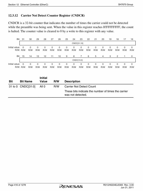
Section 12 Ethernet Controller (EtherC)
Page 416 of 1278 R01UH0234EJ0300 Rev. 3.00 Jun 21, 2011
SH7670 Group
12.3.12 Carrier Not Detect Counter Register (CNDCR)
CNDCR is a 32-bit counter that indicates the number of times the carrier could not be detected while the preamble was being sent. When the value in this register reaches H'FFFFFFFF, the count is halted. The counter value is cleared to 0 by a write to this register with any value.
31 30 29 28 27 26 25 24 23 22 21 20 19 18 17 16Bit:
Initial value:R/W:
15 14 13 12 11 10 9 8 7 6 5 4 3 2 1 0Bit:
Initial value:R/W:
0 0 0 0 0 0 0 0 0 0 0 0 0 0 0 0R/W R/W R/W R/W R/W R/W R/W R/W R/W R/W R/W R/W R/W R/W R/W R/W
0 0 0 0 0 0 0 0 0 0 0 0 0 0 0 0R/W R/W R/W R/W R/W R/W R/W R/W R/W R/W R/W R/W R/W R/W R/W R/W
CNDC[31:16]
CNDC[15:0]
Bit Bit Name Initial Value R/W Description
31 to 0 CNDC[31:0] All 0 R/W Carrier Not Detect Count
These bits indicate the number of times the carrier was not detected.

Section 12 Ethernet Controller (EtherC)
R01UH0234EJ0300 Rev. 3.00 Page 417 of 1278 Jun 21, 2011
SH7670 Group
12.3.13 CRC Error Frame Counter Register (CEFCR)
CEFCR is a 32-bit counter that indicates the number of times a frame with a CRC error was received. When the value in this register reaches H'FFFFFFFF, the count is halted. The counter value is cleared to 0 by a write to this register with any value.
31 30 29 28 27 26 25 24 23 22 21 20 19 18 17 16Bit:
Initial value:R/W:
15 14 13 12 11 10 9 8 7 6 5 4 3 2 1 0Bit:
Initial value:R/W:
0 0 0 0 0 0 0 0 0 0 0 0 0 0 0 0R/W R/W R/W R/W R/W R/W R/W R/W R/W R/W R/W R/W R/W R/W R/W R/W
0 0 0 0 0 0 0 0 0 0 0 0 0 0 0 0R/W R/W R/W R/W R/W R/W R/W R/W R/W R/W R/W R/W R/W R/W R/W R/W
CEFC[31:16]
CEFC[15:0]
Bit Bit Name Initial Value R/W Description
31 to 0 CEFC[31:0] All 0 R/W CRC Error Frame Count
These bits indicate the count of CRC error frames received.

Section 12 Ethernet Controller (EtherC)
Page 418 of 1278 R01UH0234EJ0300 Rev. 3.00 Jun 21, 2011
SH7670 Group
12.3.14 Frame Receive Error Counter Register (FRECR)
FRECR is a 32-bit counter that indicates the number of frames input from the PHY for which a receive error was indicated by the RX-ER pin. FRECR is incremented each time the RX-ER pin becomes active. When the value in this register reaches H'FFFFFFFF, the count is halted. The counter value is cleared to 0 by a write to this register with any value.
31 30 29 28 27 26 25 24 23 22 21 20 19 18 17 16Bit:
Initial value:R/W:
15 14 13 12 11 10 9 8 7 6 5 4 3 2 1 0Bit:
Initial value:R/W:
0 0 0 0 0 0 0 0 0 0 0 0 0 0 0 0R/W R/W R/W R/W R/W R/W R/W R/W R/W R/W R/W R/W R/W R/W R/W R/W
0 0 0 0 0 0 0 0 0 0 0 0 0 0 0 0R/W R/W R/W R/W R/W R/W R/W R/W R/W R/W R/W R/W R/W R/W R/W R/W
FREC[31:16]
FREC[15:0]
Bit Bit Name Initial Value R/W Description
31 to 0 FREC[31:0] All 0 R/W Frame Receive Error Count
These bits indicate the count of errors during frame reception.

Section 12 Ethernet Controller (EtherC)
R01UH0234EJ0300 Rev. 3.00 Page 419 of 1278 Jun 21, 2011
SH7670 Group
12.3.15 Too-Short Frame Receive Counter Register (TSFRCR)
TSFRCR is a 32-bit counter that indicates the number of frames of fewer than 64 bytes that have been received. When the value in this register reaches H'FFFFFFFF, the count is halted. The counter value is cleared to 0 by a write to this register with any value.
31 30 29 28 27 26 25 24 23 22 21 20 19 18 17 16Bit:
Initial value:R/W:
Bit:
Initial value:R/W:
15 14 13 12 11 10 9 8 7 6 5 4 3 2 1 0
0 0 0 0 0 0 0 0 0 0 0 0 0 0 0 0R/W R/W R/W R/W R/W R/W R/W R/W R/W R/W R/W R/W R/W R/W R/W R/W
0 0 0 0 0 0 0 0 0 0 0 0 0 0 0 0R/W R/W R/W R/W R/W R/W R/W R/W R/W R/W R/W R/W R/W R/W R/W R/W
TSFC[31:16]
TSFC[15:0]
Bit Bit Name Initial Value R/W Description
31 to 0 TSFC[31:0] All 0 R/W Too-Short Frame Receive Count
These bits indicate the count of frames received with a length of less than 64 bytes.
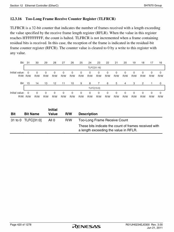
Section 12 Ethernet Controller (EtherC)
Page 420 of 1278 R01UH0234EJ0300 Rev. 3.00 Jun 21, 2011
SH7670 Group
12.3.16 Too-Long Frame Receive Counter Register (TLFRCR)
TLFRCR is a 32-bit counter that indicates the number of frames received with a length exceeding the value specified by the receive frame length register (RFLR). When the value in this register reaches H'FFFFFFFF, the count is halted. TLFRCR is not incremented when a frame containing residual bits is received. In this case, the reception of the frame is indicated in the residual-bit frame counter register (RFCR). The counter value is cleared to 0 by a write to this register with any value.
31 30 29 28 27 26 25 24 23 22 21 20 19 18 17 16Bit:
Initial value:R/W:
15 14 13 12 11 10 9 8 7 6 5 4 3 2 1 0Bit:
Initial value:R/W:
0 0 0 0 0 0 0 0 0 0 0 0 0 0 0 0R/W R/W R/W R/W R/W R/W R/W R/W R/W R/W R/W R/W R/W R/W R/W R/W
0 0 0 0 0 0 0 0 0 0 0 0 0 0 0 0R/W R/W R/W R/W R/W R/W R/W R/W R/W R/W R/W R/W R/W R/W R/W R/W
TLFC[31:16]
TLFC[15:0]
Bit Bit Name Initial Value R/W Description
31 to 0 TLFC[31:0] All 0 R/W Too-Long Frame Receive Count
These bits indicate the count of frames received with a length exceeding the value in RFLR.

Section 12 Ethernet Controller (EtherC)
R01UH0234EJ0300 Rev. 3.00 Page 421 of 1278 Jun 21, 2011
SH7670 Group
12.3.17 Residual-Bit Frame Counter Register (RFCR)
RFCR is a 32-bit counter that indicates the number of frames received containing residual bits (less than an 8-bit unit). When the value in this register reaches H'FFFFFFFF, the count is halted. The counter value is cleared to 0 by a write to this register with any value.
31 30 29 28 27 26 25 24 23 22 21 20 19 18 17 16Bit:
Initial value:R/W:
15 14 13 12 11 10 9 8 7 6 5 4 3 2 1 0Bit:
Initial value:R/W:
0 0 0 0 0 0 0 0 0 0 0 0 0 0 0 0R/W R/W R/W R/W R/W R/W R/W R/W R/W R/W R/W R/W R/W R/W R/W R/W
0 0 0 0 0 0 0 0 0 0 0 0 0 0 0 0R/W R/W R/W R/W R/W R/W R/W R/W R/W R/W R/W R/W R/W R/W R/W R/W
RFC[31:16]
RFC[15:0]
Bit Bit Name Initial Value R/W Description
31 to 0 RFC[31:0] All 0 R/W Residual-Bit Frame Count
These bits indicate the count of frames received containing residual bits.

Section 12 Ethernet Controller (EtherC)
Page 422 of 1278 R01UH0234EJ0300 Rev. 3.00 Jun 21, 2011
SH7670 Group
12.3.18 Multicast Address Frame Counter Register (MAFCR)
MAFCR is a 32-bit counter that indicates the number of frames received with a specified multicast address. When the value in this register reaches H'FFFFFFFF, the count is halted. The counter value is cleared to 0 by a write to this register with any value.
31 30 29 28 27 26 25 24 23 22 21 20 19 18 17 16Bit:
Initial value:R/W:
15 14 13 12 11 10 9 8 7 6 5 4 3 2 1 0Bit:
Initial value:R/W:
0 0 0 0 0 0 0 0 0 0 0 0 0 0 0 0R/W R/W R/W R/W R/W R/W R/W R/W R/W R/W R/W R/W R/W R/W R/W R/W
0 0 0 0 0 0 0 0 0 0 0 0 0 0 0 0R/W R/W R/W R/W R/W R/W R/W R/W R/W R/W R/W R/W R/W R/W R/W R/W
MAFC[31:16]
MAFC[15:0]
Bit Bit Name Initial Value R/W Description
31 to 0 MAFC[31:0] All 0 R/W Multicast Address Frame Count
These bits indicate the count of multicast frames received.
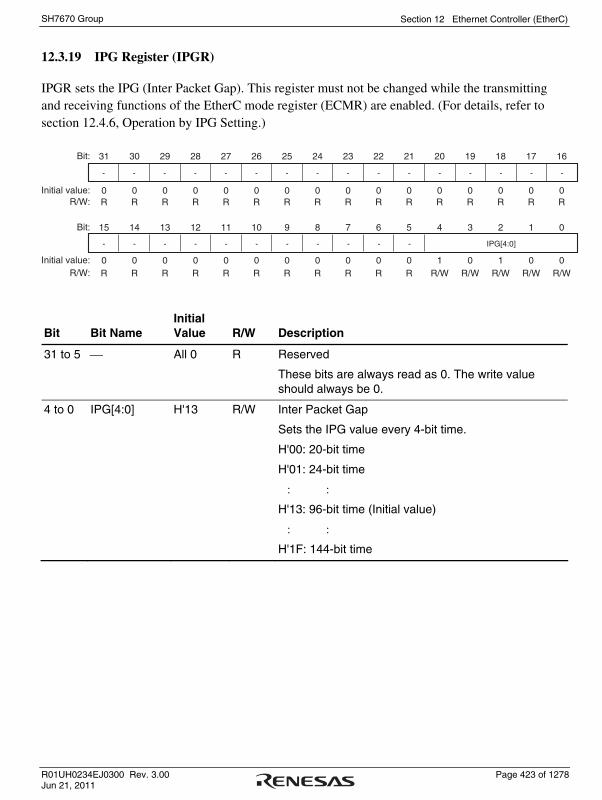
Section 12 Ethernet Controller (EtherC)
R01UH0234EJ0300 Rev. 3.00 Page 423 of 1278 Jun 21, 2011
SH7670 Group
12.3.19 IPG Register (IPGR)
IPGR sets the IPG (Inter Packet Gap). This register must not be changed while the transmitting and receiving functions of the EtherC mode register (ECMR) are enabled. (For details, refer to section 12.4.6, Operation by IPG Setting.)
31 30 29 28 27 26 25 24 23 22 21 20 19 18 17 16Bit:
Initial value:R/W:
15 14 13 12 11 10 9 8 7 6 5 4 3 2 1 0Bit:
Initial value:R/W:
0 0 0 0 0 0 0 0 0 0 0 0 0 0 0 0R R R R R R R R R R R R R R R R
0 0 0 0 0 0 0 0 0 0 0 1 0 1 0 0R R R R R R R R R R R R/W R/W R/W R/W R/W
- - - - - - - - - - - - - - - -
- - - - - - - - - - - IPG[4:0]
Bit Bit Name Initial Value R/W Description
31 to 5 ⎯ All 0 R Reserved
These bits are always read as 0. The write value should always be 0.
4 to 0 IPG[4:0] H'13 R/W Inter Packet Gap
Sets the IPG value every 4-bit time.
H'00: 20-bit time
H'01: 24-bit time
: :
H'13: 96-bit time (Initial value)
: :
H'1F: 144-bit time

Section 12 Ethernet Controller (EtherC)
Page 424 of 1278 R01UH0234EJ0300 Rev. 3.00 Jun 21, 2011
SH7670 Group
12.3.20 Automatic PAUSE Frame Set Register (APR)
APR sets the TIME parameter value of the automatic PAUSE frame. When transmitting the automatic PAUSE frame, the value set in this register is used as the TIME parameter of the PAUSE frame.
31 30 29 28 27 26 25 24 23 22 21 20 19 18 17 16Bit:
Initial value:R/W:
15 14 13 12 11 10 9 8 7 6 5 4 3 2 1 0Bit:
Initial value:R/W:
0 0 0 0 0 0 0 0 0 0 0 0 0 0 0 0R R R R R R R R R R R R R R R R
0 0 0 0 0 0 0 0 0 0 0 0 0 0 0 0R/W R/W R/W R/W R/W R/W R/W R/W R/W R/W R/W R/W R/W R/W R/W R/W
- - - - - - - - - - - - - - - -
AP[15:0]
Bit Bit Name Initial Value R/W Description
31 to 16 ⎯ All 0 R Reserved
These bits are always read as 0. The write value should always be 0.
15 to 0 AP[15:0] All 0 R/W Automatic PAUSE
Sets the TIME parameter value of the automatic PAUSE frame. At this time, 1 bit means 512-bit time.
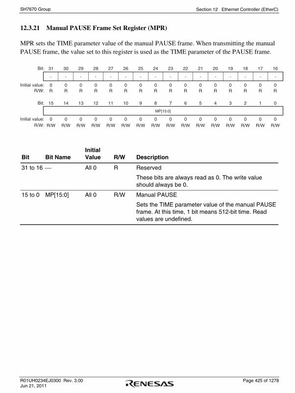
Section 12 Ethernet Controller (EtherC)
R01UH0234EJ0300 Rev. 3.00 Page 425 of 1278 Jun 21, 2011
SH7670 Group
12.3.21 Manual PAUSE Frame Set Register (MPR)
MPR sets the TIME parameter value of the manual PAUSE frame. When transmitting the manual PAUSE frame, the value set to this register is used as the TIME parameter of the PAUSE frame.
31 30 29 28 27 26 25 24 23 22 21 20 19 18 17 16Bit:
Initial value:R/W:
15 14 13 12 11 10 9 8 7 6 5 4 3 2 1 0Bit:
Initial value:R/W:
0 0 0 0 0 0 0 0 0 0 0 0 0 0 0 0R R R R R R R R R R R R R R R R
0 0 0 0 0 0 0 0 0 0 0 0 0 0 0 0R/W R/W R/W R/W R/W R/W R/W R/W R/W R/W R/W R/W R/W R/W R/W R/W
- - - - - - - - - - - - - - - -
MP[15:0]
Bit Bit Name Initial Value R/W Description
31 to 16 ⎯ All 0 R Reserved
These bits are always read as 0. The write value should always be 0.
15 to 0 MP[15:0] All 0 R/W Manual PAUSE
Sets the TIME parameter value of the manual PAUSE frame. At this time, 1 bit means 512-bit time. Read values are undefined.

Section 12 Ethernet Controller (EtherC)
Page 426 of 1278 R01UH0234EJ0300 Rev. 3.00 Jun 21, 2011
SH7670 Group
12.3.22 PAUSE Frame Retransfer Count Set Register (TPAUSER)
TPAUSER sets the upper limit of the number of times of the PAUSE frame retransfer. TPAUSER must not be changed while the transmitting function is enabled.
31 30 29 28 27 26 25 24 23 22 21 20 19 18 17 16Bit:
Initial value:R/W:
15 14 13 12 11 10 9 8 7 6 5 4 3 2 1 0Bit:
Initial value:R/W:
0 0 0 0 0 0 0 0 0 0 0 0 0 0 0 0R R R R R R R R R R R R R R R R
0 0 0 0 0 0 0 0 0 0 0 0 0 0 0 0R/W R/W R/W R/W R/W R/W R/W R/W R/W R/W R/W R/W R/W R/W R/W R/W
- - - - - - - - - - - - - - - -
TPAUSE[15:0]
Bit Bit Name Initial Value R/W Description
31 to 16 ⎯ All 0 R Reserved
These bits are always read as 0. The write value should always be 0.
15 to 0 TPAUSE[15:0] All 0 R/W Upper Limit of the Number of Times of PAUSE Frame Retransfer
H'0000: Unlimited number of times of retransfer
H'0001: Retransfer once
: :
H'FFFF: Number of times of retransfer is 65535

Section 12 Ethernet Controller (EtherC)
R01UH0234EJ0300 Rev. 3.00 Page 427 of 1278 Jun 21, 2011
SH7670 Group
12.4 Operation
The overview of the Ethernet controller (EtherC) are shown below. The EtherC transmits and receives PAUSE frames conforming to the Ethernet/IEEE802.3 frames.
12.4.1 Transmission
The EtherC transmitter assembles the transmit data on the frame and outputs to MII when there is a transmit request from the E-DMAC. The data transmitted via the MII is transmitted to the lines by PHY-LSI. Figure 12.2 shows the state transition of the EtherC transmitter.

Section 12 Ethernet Controller (EtherC)
Page 428 of 1278 R01UH0234EJ0300 Rev. 3.00 Jun 21, 2011
SH7670 Group
FDPX
FDPX
HDPX
HDPX
Collision
Collision
Collision*2
Collision*2
Error
Error
Error
Normal transmission
Notes: 1. Transmission retry processing includes both jam transmission that depends on collision detection and the adjustment of transmission intervals based on the back-off algorithm. 2. Transmission is retried only when data of 512 bits or less (including the preamble and SFD) is transmitted. When a collision is detected during the transmission of data greater than 512 bits, only jam is transmitted and transmission based on the back-off algorithm is not retried.
Error notification
Transmission halted
Start of transmission (preamble transmission)
Carrier detection
Carrier detection
SFD transmission
CRC transmission
Data transmission
Carrier detection
Failure of 15 retransfer attempts
or collision after 512-bit time
Retransfer processing*1
Error detection
Retransfer initiation
Carrier non-detection
Carrier non-detection
IdleTE set
TE reset
Reset
[Legend]FDPX: Full DuplexHDPX: Half DuplexSFD: Start Frame Delimiter
Figure 12.2 EtherC Transmitter State Transitions
1. When the transmit enable (TE) bit is set, the transmitter enters the transmit idle state.
2. When a transmit request is issued by the transmit E-DMAC, the EtherC sends the preamble after a transmission delay equivalent to the frame interval time. If full-duplex transfer is selected, which does not require carrier detection, the preamble is sent as soon as a transmit request is issued by the E-DMAC.

Section 12 Ethernet Controller (EtherC)
R01UH0234EJ0300 Rev. 3.00 Page 429 of 1278 Jun 21, 2011
SH7670 Group
3. The transmitter sends the SFD, data, and CRC sequentially. At the end of transmission, the transmit E-DMAC generates a transmission complete interrupt (TC). If a collision or the carrier-not-detected state occurs during data transmission, these are reported as interrupt sources.
4. After waiting for the frame interval time, the transmitter enters the idle state, and if there is more transmit data, continues transmitting.
12.4.2 Reception
The EtherC receiver separates the frame data (MII into preamble, SFD, DA (destination address), SA (Source address), type/length, Data, and CRC data) and outputs DA, SA, type/length, Data to the E-DMAC. Figure 12.3 shows the state transitions of the EtherC receiver.
Illegal carrier detection
Start of frame reception
Wait for SFD reception
Data reception
CRC reception
Destination address reception
Preamble detection
Reception halted
Reset
Error notification*
RE set
[Legend]SFD: Start frame delimiterNote: * The error frame also transmits data to the buffer.
End of reception
Receive error detection
Receive error detection
Error detection
Promiscuous and other station destination address
RE reset
Normal reception
Idle
RX-DV negation
SFD reception
Own destination addressor broadcastor multicastor promiscuous
Figure 12.3 EtherC Receiver State Transmissions

Section 12 Ethernet Controller (EtherC)
Page 430 of 1278 R01UH0234EJ0300 Rev. 3.00 Jun 21, 2011
SH7670 Group
1. When the receive enable (RE) bit is set, the receiver enters the receive idle state.
2. When an SFD (start frame delimiter) is detected after a receive packet preamble, the receiver starts receive processing. Discards a frame with an invalid pattern.
3. In normal mode, if the destination address matches the receiver’s own address, or if broadcast or multicast transmission or promiscuous mode is specified, the receiver starts data reception.
4. Following data reception from the MII, the receiver carries out a CRC check. The result is indicated as a status bit in the descriptor after the frame data has been written to memory. Reports an error status in the case of an abnormality.
5. After one frame has been received, if the receive enable bit is set (RE = 1) in the EtherC mode register, the receiver prepares to receive the next frame.
12.4.3 MII Frame Timing
Each MII Frame timing is shown in figure 12.4.
TX-CLK
TX-EN
TXD3 to TXD0
TX-ER
CRS
COL
SFDPreamble Data CRC
Figure 12.4 (1) MII Frame Transmit Timing (Normal Transmission)
TX-CLK
TX-EN
TX-ER
CRS
COL
Preamble JAMMII_TXD3 toMII_TXD0
Figure 12.4 (2) MII Frame Transmit Timing (Collision)

Section 12 Ethernet Controller (EtherC)
R01UH0234EJ0300 Rev. 3.00 Page 431 of 1278 Jun 21, 2011
SH7670 Group
TX-CLK
TX-EN
MII_TXD3 toMII_TXD0
TX-ER
CRS
COL
SFDPreamble Data
Figure 12.4 (3) MII Frame Transmit Timing (Transmit Error)
RX-CLK
RX-DV
RX-ER
Preamble Data CRCSFDMII_RXD3 toMII_RXD0
Figure 12.4 (4) MII Frame Receive Timing (Normal Reception)
RX-CLK
RX-DV
RX-ER
Preamble Data XXXXSFDMII_RXD3 toMII_RXD0
Figure 12.4 (5) MII Frame Receive Timing (Reception Error (1))
RX-CLK
RX-DV
RX-ER
XXXX 1110 XXXXMII_RXD3 to
MII_RXD0
Figure 12.4 (6) MII Fame Receive Timing (Reception Error (2))

Section 12 Ethernet Controller (EtherC)
Page 432 of 1278 R01UH0234EJ0300 Rev. 3.00 Jun 21, 2011
SH7670 Group
12.4.4 Accessing MII Registers
MII registers in the PHY are accessed via this LSI’s PHY interface register (PIR). Connection is made as a serial interface in accordance with the MII frame format specified in IEEE802.3u.
MII Management Frame Format: The format of an MII management frame is shown in figure 12.5. To access an MII register, a management frame is implemented by the program in accordance with the procedures shown in MII Register Access Procedure.
Access Type MII Management Frame
Item
Number of bits
Read
Write
PRE
32
1..1
1..1
ST
2
01
01
OP
2
10
01
PHYAD
5
00001
00001
REGAD
5
RRRRR
RRRRR
TA
2
Z0
10
DATA
16
D..D
D..D
IDLE
X
PRE:ST:OP:PHYAD:
REGAD:
TA:
DATA:
IDLE:
[Legend]32 consecutive 1sWrite of 01 indicating start of frameWrite of code indicating access typeWrite of 0001 if the PHY address is 1 (sequential write starting with the MSB). This bit changes depending on the PHY address.Write of 0001 if the register address is 1 (sequential write starting with the MSB). This bit changes depending on the PHY register address.Time for switching data transmission source on MII interface(a) Write: 10 written(b) Read: Bus release (notation: Z0) performed16-bit data. Sequential write or read from MSB(a) Write: 16-bit data write(b) Read: 16-bit data readWait time until next MII management format input(a) Write: Independent bus release (notation: X) performed(b) Read: Bus already released in TA; control unnecessary
Figure 12.5 MII Management Frame Format

Section 12 Ethernet Controller (EtherC)
R01UH0234EJ0300 Rev. 3.00 Page 433 of 1278 Jun 21, 2011
SH7670 Group
MII Register Access Procedure: The program accesses MII registers via the PHY interface register (PIR). Access is implemented by a combination of 1-bit-unit data write, 1-bit-unit data read, bus release, and independent bus release. Figure 12.6 shows the MII register access timing. The timing will differ depending on the PHY type.
MDC
(1)
(1) (2) (3)
MDO
(2)
(3)
Write to PHY interfaceregister
1-bit data write timingrelationship
MMD = 1MDO = write dataMDC = 0
MMD = 1MDO = write dataMDC = 1
Write to PHY interfaceregister
MMD = 1MDO = write dataMDC = 0
Write to PHY interfaceregister
Figure 12.6 (1) 1-Bit Data Write Flowchart
MDC
(1)
(1) (2) (3)
Write to PHY interfaceregister
MMD = 0MDC = 0
Bus release timingrelationship
MDO
(2) Write to PHY interfaceregister
MMD = 0MDC = 1
(3) Write to PHY interfaceregister
MMD = 0MDC = 0
Figure 12.6 (2) Bus Release Flowchart (TA in Read in Figure 12.5)

Section 12 Ethernet Controller (EtherC)
Page 434 of 1278 R01UH0234EJ0300 Rev. 3.00 Jun 21, 2011
SH7670 Group
MDC
(1)
(1) (2) (3)
Write to PHY interfaceregister
MMD = 0 MDC = 1
1-bit data read timingrelationship
(3) Write to PHY interfaceregister
MMD = 0 MDC = 0
(2) Read from PHYinterface register read
MMD = 0MMC = 1
MDI is read data
MDI
Figure 12.6 (3) 1-Bit Data Read Flowchart
MDC
(1)
(1)
Write to PHY interfaceregister
MMD = 0MDC = 0
Independent bus releasetiming relationship
MDO
Figure 12.6 (4) Independent Bus Release Flowchart (IDLE in Write in Figure 12.5)

Section 12 Ethernet Controller (EtherC)
R01UH0234EJ0300 Rev. 3.00 Page 435 of 1278 Jun 21, 2011
SH7670 Group
12.4.5 Magic Packet Detection
The EtherC has a Magic Packet detection function. This function provides a Wake-On-LAN (WOL) facility that activates various peripheral devices connected to a LAN from the host device or other source. This makes it possible to construct a system in which a peripheral device receives a Magic Packet sent from the host device or other source, and activates itself. When the Magic Packet is detected, data is stored in the FIFO of the E-DMAC by the broadcast packet that has received data previously and the EtherC is notified of the receiving status. To return to normal operation from the interrupt processing, initialize the EtherC and E-DMAC by using the SWR bit in the E-DMAC mode register (EDMR).
With a Magic Packet, reception is performed regardless of the destination address. As a result, this function is valid, and the WOL pin enabled, only in the case of a match with the destination address specified by the format in the Magic Packet. Further information on Magic Packets can be found in the technical documentation published by AMD Corporation.
The procedure for using the WOL function with this LSI is as follows.
1. Disable interrupt source output by means of the various interrupt enable/mask registers.
2. Set the Magic Packet detection enable bit (MPDE) in the EtherC mode register (ECMR).
3. Set the Magic Packet detection interrupt enable bit (MPDIP) in the EtherC interrupt enable register (ECSIPR) and clear the other bits in ECSIPR. Set the EtherC status register interrupt permission bit (ECIIP) of the EtherC/E-DMAC status interrupt permission register (EESIPR) in the Ethernet controller direct memory access controller (E-DMAC) and clear the other bits in EESIPR.
4. If necessary, set the CPU operating mode to sleep mode or set supporting functions to module standby mode.
5. When a Magic Packet is detected, an interrupt is sent to the CPU. The WOL pin notifies peripheral LSIs that the Magic Packet has been detected.

Section 12 Ethernet Controller (EtherC)
Page 436 of 1278 R01UH0234EJ0300 Rev. 3.00 Jun 21, 2011
SH7670 Group
12.4.6 Operation by IPG Setting
The EtherC has a function to change the non-transmission period IPG (Inter Packet Gap) between transmit frames. By changing the set values of the IPG setting register (IPGR), the transmission efficiency can be raised and lowered from the standard value. IPG settings are prescribed in IEEE802.3 standards. When changing settings, adequately check that the respective devices can operate smoothly on the same network.
IPG*
[1] [2] [3] [4]
[1] [2] [3] [4]
[5] ......
......
Packet
Note: * IPG may be longer than the set value, depending on the state of the circuit and the system bus.
Case A (short IPG)
Case B (long IPG)
Figure 12.7 Changing IPG and Transmission Efficiency
12.4.7 Flow Control
The EtherC supports flow control functions conforming to IEEE802.3x in full-duplex operations. Flow control can be applied to both receive and transmit operations. The methods for transmitting PAUSE frames when controlling flow are as follows:
Automatic PAUSE Frame Transmission: For receive frames, PAUSE frames are automatically transmitted when the number of data in the receive FIFO (included in E-DMAC) reaches the value set in the flow control FIFO threshold register (FCFTR) of the E-DMAC. The TIME parameter included in the PAUSE frame at this time is set by the automatic PAUSE frame setting register (APR). The automatic PAUSE frame transmission is repeated until the number of data in the receive FIFO becomes less than the FCFTR setting as the receive data is read from the FIFO.
The upper limit of the number of retransfers of the PAUSE frame can also be set by the automatic PAUSE frame retransfer count set register (TPAUSER). In this case, PAUSE frame transmission is repeated until the number of data becomes FCFTR value set or below, or the number of transmits reaches the value set by TPAUSER. The automatic PAUSE frame transmission is enabled when the TXF bit in the EtherC mode register (ECMR) is 1.

Section 12 Ethernet Controller (EtherC)
R01UH0234EJ0300 Rev. 3.00 Page 437 of 1278 Jun 21, 2011
SH7670 Group
Manual PAUSE Frame Transmission: PAUSE frames are transmitted by directives from the software. When writing the Timer value to the manual PAUSE frame set register (MPR), manual PAUSE frame transmission is started. With this method, PAUSE frame transmission is carried out only once.
PAUSE Frame Reception: The next frame is not transmitted until the time indicated by the Timer value elapses after receiving a PAUSE frame. However, the transmission of the current frame is continued. A received PAUSE frame is valid only when the RXF bit in the EtherC mode register (ECMR) is set to 1.
12.5 Connection to PHY-LSI
Figure 12.8 shows the example of connection to a DP83846AVHG by National Semiconductor Corporation.
TX-ERMII_TXD3MII_TXD2MII_TXD1MII_TXD0
TX-ENTX-CLK
MDCMDIO
MII_RXD3MII_RXD2MII_RXD1MII_RXD0
RX-CLKCRSCOL
RX-DVRX-ER
TX_ERTXD3TXD2TXD1TXD0TX_ENTX_CLKMDCMDIORXD3RXD2RXD1RXD0RX_CLKCRSCOLRX_DVRX_ER
DP83846AVHGMII (Media Independent Interface)
This LSI
Figure 12.8 Example of Connection to DP83846AVHG

Section 12 Ethernet Controller (EtherC)
Page 438 of 1278 R01UH0234EJ0300 Rev. 3.00 Jun 21, 2011
SH7670 Group
12.6 Usage Notes
• Conditions for Setting LCHNG Bit
Even if the level of the signal input to the LNKSTA pin is not changed, the LCHNG bit in ECSR may be set. It may happen when the pin function is changed from port to LNKSTA by PCCRH2 of the PFC or when a software reset caused by the SWR bit in EDMR is cleared while the LNKSTA pin is being driven high.
This is because the LNKSTA signal is internally fixed low when the pin functions as a port or during the software reset state regardless of the external pin level.
Clear the LCHNG bit before setting the LCHNGIP bit in ECSIPR not to request a LINK signal changed interrupt accidentally.

Section 13 Ethernet Controller Direct Memory Access Controller (E-DMAC)
R01UH0234EJ0300 Rev. 3.00 Page 439 of 1278 Jun 21, 2011
SH7670 Group
Section 13 Ethernet Controller Direct Memory Access Controller (E-DMAC)
This LSI includes a direct memory access controller (E-DMAC) directly connected to the Ethernet controller (EtherC). A large proportion of buffer management is controlled by the E-DMAC itself using descriptors. This lightens the load on the CPU and enables efficient control of data transfer.
Figure 13.1 shows the configuration of the E-DMAC, and the descriptors and transmit/receive buffers in memory.
13.1 Features
The E-DMAC has the following features:
• The load on the CPU is reduced by means of a descriptor management system
• Transmit/receive frame status information is indicated in descriptors
• Achieves efficient system bus utilization through the use of block transfer (16-byte units)
• Supports single-frame/multi-buffer operation
Transmit FIFO
Receive FIFO
Transmitdescriptor
Transmitbuffer
Receivebuffer
Receivedescriptor
External businterface
Internal bus
Internal businterface
This LSI
External memory
EtherC
E-DMACDescriptorinformationTransmitDMAC
ReceiveDMAC
Descriptorinformation
Figure 13.1 Configuration of E-DMAC, and Descriptors and Buffers

Section 13 Ethernet Controller Direct Memory Access Controller (E-DMAC)
Page 440 of 1278 R01UH0234EJ0300 Rev. 3.00 Jun 21, 2011
SH7670 Group
13.2 Register Descriptions
The E-DMAC has the following registers. For addresses and access sizes of these registers, see section 28, List of Registers.
• E-DMAC mode register (EDMR)
• E-DMAC transmit request register (EDTRR)
• E-DMAC receive request register (EDRRR)
• Transmit descriptor list address register (TDLAR)
• Receive descriptor list address register (RDLAR)
• EtherC/E-DMAC status register (EESR)
• EtherC/E-DMAC status interrupt permission register (EESIPR)
• Transmit/receive status copy enable register (TRSCER)
• Receive missed-frame counter register (RMFCR)
• Transmit FIFO threshold register (TFTR)
• FIFO depth register (FDR)
• Receiving method control register (RMCR)
• E-DMAC operation control register (EDOCR)
• Receive buffer write address register (RBWAR)
• Receive descriptor fetch address register (RDFAR)
• Transmit buffer read address register (TBRAR)
• Transmit descriptor fetch address register (TDFAR)
• Flow control FIFO threshold register (FCFTR)
• Receive data padding setting register (RPADIR)
• Transmit interrupt register (TRIMD)
• Checksum mode register (CSMR)
• Checksum skipped bytes monitor register (CSSBM)
• Checksum monitor register (CSSMR)
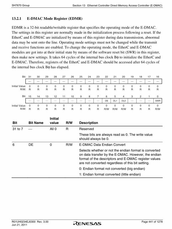
Section 13 Ethernet Controller Direct Memory Access Controller (E-DMAC)
R01UH0234EJ0300 Rev. 3.00 Page 441 of 1278 Jun 21, 2011
SH7670 Group
13.2.1 E-DMAC Mode Register (EDMR)
EDMR is a 32-bit readable/writable register that specifies the operating mode of the E-DMAC. The settings in this register are normally made in the initialization process following a reset. If the EtherC and E-DMAC are initialized by means of this register during data transmission, abnormal data may be sent onto the line. Operating mode settings must not be changed while the transmit and receive functions are enabled. To change the operating mode, the EtherC and E-DMAC modules are got into at their initial state by means of the software reset bit (SWR) in this register, then make new settings. It takes 64 cycles of the internal bus clock Bφ to initialize the EtherC and E-DMAC. Therefore, registers of the EtherC and E-DMAC should be accessed after 64 cycles of the internal bus clock Bφ has elapsed.
31 30 29 28 27 26 25 24 23 22 21 20 19 18 17 16Bit:
Initial Value:R/W:
Bit:
Initial Value:R/W:
15 14 13 12 11 10 9 8 7 6 5 4 3 2 1 0
0 0 0 0 0 0 0 0 0 0 0 0 0 0 0 0R R R R R R R R R R R R R R R R
0 0 0 0 0 0 0 0 0 0 0 0 0 0 0 0R R R R R R R R R R/W R/W R/W R R R R/W
⎯ ⎯ ⎯ ⎯ ⎯ ⎯ ⎯ ⎯ ⎯ ⎯ ⎯ ⎯ ⎯ ⎯ ⎯ ⎯
⎯ ⎯ ⎯ ⎯ ⎯ ⎯ ⎯ ⎯ ⎯ DE DL1 DL0 ⎯ ⎯ ⎯ SWR
Bit Bit Name Initial value R/W Description
31 to 7 ⎯ All 0 R Reserved
These bits are always read as 0. The write value should always be 0.
6 DE 0 R/W E-DMAC Data Endian Convert
Selects whether or not the endian format is converted on data transfer by the E-DMAC. However, the endian format of the descriptors and E-DMAC register values are not converted regardless of this bit setting.
0: Endian format not converted (big endian)
1: Endian format converted (little endian)
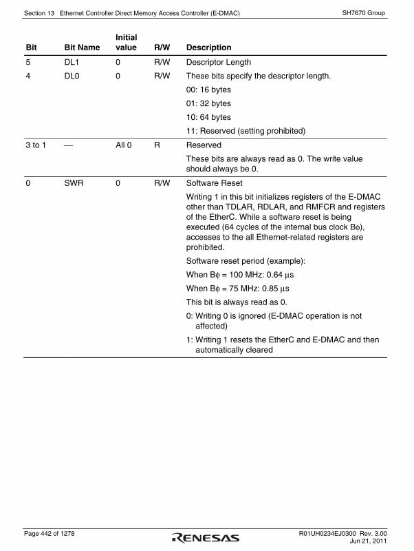
Section 13 Ethernet Controller Direct Memory Access Controller (E-DMAC)
Page 442 of 1278 R01UH0234EJ0300 Rev. 3.00 Jun 21, 2011
SH7670 Group
Bit Bit Name Initial value R/W Description
5
4
DL1
DL0
0
0
R/W
R/W
Descriptor Length
These bits specify the descriptor length.
00: 16 bytes
01: 32 bytes
10: 64 bytes
11: Reserved (setting prohibited)
3 to 1 ⎯ All 0 R Reserved
These bits are always read as 0. The write value should always be 0.
0 SWR 0 R/W Software Reset
Writing 1 in this bit initializes registers of the E-DMAC other than TDLAR, RDLAR, and RMFCR and registers of the EtherC. While a software reset is being executed (64 cycles of the internal bus clock Bφ), accesses to the all Ethernet-related registers are prohibited.
Software reset period (example):
When Bφ = 100 MHz: 0.64 μs
When Bφ = 75 MHz: 0.85 μs
This bit is always read as 0.
0: Writing 0 is ignored (E-DMAC operation is not affected)
1: Writing 1 resets the EtherC and E-DMAC and then automatically cleared

Section 13 Ethernet Controller Direct Memory Access Controller (E-DMAC)
R01UH0234EJ0300 Rev. 3.00 Page 443 of 1278 Jun 21, 2011
SH7670 Group
13.2.2 E-DMAC Transmit Request Register (EDTRR)
The EDTRR is a 32-bit readable/writable register that issues transmit directives to the E-DMAC. When transmission of one frame is completed, the next descriptor is read. If the transmit descriptor active bit in this descriptor has the "active" setting, transmission is continued. If the transmit descriptor active bit has the "inactive" setting, the TR bit is cleared and operation of the transmit DMAC is halted.
31 30 29 28 27 26 25 24 23 22 21 20 19 18 17 16Bit:
Initial Value:R/W:
Bit:
Initial Value:R/W:
15 14 13 12 11 10 9 8 7 6 5 4 3 2 1 0
0 0 0 0 0 0 0 0 0 0 0 0 0 0 0 0R R R R R R R R R R R R R R R R
0 0 0 0 0 0 0 0 0 0 0 0 0 0 0 0R R R R R R R R R R R R R R R R/W
⎯ ⎯ ⎯ ⎯ ⎯ ⎯ ⎯ ⎯ ⎯ ⎯ ⎯ ⎯ ⎯ ⎯ ⎯ ⎯
⎯ ⎯ ⎯ ⎯ ⎯ ⎯ ⎯ ⎯ ⎯ ⎯ ⎯ ⎯ ⎯ ⎯ ⎯ TR
Bit Bit Name Initial value R/W Description
31 to 1 ⎯ All 0 R Reserved
These bits are always read as 0. The write value should always be 0.
0 TR 0 R/W Transmit Request
0: Transmission-halted state. Writing 0 does not stop transmission. Termination of transmission is controlled by the active bit in the transmit descriptor
1: Start of transmission. The relevant descriptor is read and a frame is sent with the transmit active bit set to 1

Section 13 Ethernet Controller Direct Memory Access Controller (E-DMAC)
Page 444 of 1278 R01UH0234EJ0300 Rev. 3.00 Jun 21, 2011
SH7670 Group
13.2.3 E-DMAC Receive Request Register (EDRRR)
EDRRR is a 32-bit readable/writable register that issues receive directives to the E-DMAC. When the receive request bit is set, the E-DMAC reads the relevant receive descriptor. If the receive descriptor active bit in the descriptor has the "active" setting, the E-DMAC prepares for a receive request from the EtherC. When one receive buffer of data has been received, the E-DMAC reads the next descriptor and prepares to receive the next frame. If the receive descriptor active bit in the descriptor has the "inactive" setting, the RR bit is cleared and operation of the receive DMAC is halted.
31 30 29 28 27 26 25 24 23 22 21 20 19 18 17 16Bit:
Initial Value:
R/W:
15 14 13 12 11 10 9 8 7 6 5 4 3 2 1 0
0 0 0 0 0 0 0 0 0 0 0 0 0 0 0 0R R R R R R R R R R R R R R R R
0 0 0 0 0 0 0 0 0 0 0 0 0 0 0 0R R R R R R R R R R R R R R R R/W
⎯ ⎯ ⎯ ⎯ ⎯ ⎯ ⎯ ⎯ ⎯ ⎯ ⎯ ⎯ ⎯ ⎯ ⎯
⎯ ⎯ ⎯ ⎯ ⎯ ⎯ ⎯ ⎯ ⎯ ⎯ ⎯ ⎯ ⎯ ⎯ ⎯
⎯
RR
Bit Bit Name Initial value R/W Description
31 to 1 ⎯ All 0 R Reserved
These bits are always read as 0. The write value should always be 0.
0 RR 0 R/W Receive Request
0: The receive function is disabled*
1: A receive descriptor is read and the E-DMAC is ready to receive
Note: * If the receive function is disabled during frame reception, write-back is not performed successfully to the receive descriptor. Following pointers to read a receive descriptor become abnormal and the E-DMAC cannot operate successfully. In this case, to make the E-DMAC reception enabled again, execute a software reset by the SWR bit in EDMR. To make the E-DMAC reception disabled without executing a software reset, set the RE bit in ECMR. Next, after the E_DMAC has completed the reception and write-back to the receive descriptor has been confirmed, disable the receive function of this register.

Section 13 Ethernet Controller Direct Memory Access Controller (E-DMAC)
R01UH0234EJ0300 Rev. 3.00 Page 445 of 1278 Jun 21, 2011
SH7670 Group
13.2.4 Transmit Descriptor List Address Register (TDLAR)
TDLAR is a 32-bit readable/writable register that specifies the start address of the transmit descriptor list. Descriptors have a boundary configuration in accordance with the descriptor length indicated by the DL bit in EDMR. This register must not be written to during transmission. Modifications to this register should only be made while transmission is disabled by the TR bit (= 0) in the E-DMAC transmit request register (EDTRR).
31 30 29 28 27 26 25 24 23 22 21 20 19 18 17 16Bit:
Initial Value:R/W:
15 14 13 12 11 10 9 8 7 6 5 4 3 2 1 0Bit:
Initial Value:R/W:
0 0 0 0 0 0 0 0 0 0 0 0 0 0 0 0R/W R/W R/W R/W R/W R/W R/W R/W R/W R/W R/W R/W R/W R/W R/W R/W
0 0 0 0 0 0 0 0 0 0 0 0 0 0 0 0R/W R/W R/W R/W R/W R/W R/W R/W R/W R/W R/W R/W R/W R/W R/W R/W
TDLA[31:16]
TDLA[15:0]
Bit Bit Name Initial value R/W Description
31 to 0 TDLA[31:0] All 0 R/W Transmit Descriptor Start Address
The lower bits are set as follows according to the specified descriptor length.
16-byte boundary: TDLA3 to TDLA0 = 0000
32-byte boundary: TDLA4 to TDLA0 = 00000
64-byte boundary: TDLA5 to TDLA0 = 000000

Section 13 Ethernet Controller Direct Memory Access Controller (E-DMAC)
Page 446 of 1278 R01UH0234EJ0300 Rev. 3.00 Jun 21, 2011
SH7670 Group
13.2.5 Receive Descriptor List Address Register (RDLAR)
RDLAR is a 32-bit readable/writable register that specifies the start address of the receive descriptor list. Descriptors have a boundary configuration in accordance with the descriptor length indicated by the DL bit in EDMR. This register must not be written to during reception. Modifications to this register should only be made while reception is disabled by the RR bit (= 0) in the E-DMAC Receive Request Register (EDRRR).
31 30 29 28 27 26 25 24 23 22 21 20 19 18 17 16Bit:
Initial Value:R/W:
Bit:
Initial Value:R/W:
15 14 13 12 11 10 9 8 7 6 5 4 3 2 1 0
0 0 0 0 0 0 0 0 0 0 0 0 0 0 0 0R/W R/W R/W R/W R/W R/W R/W R/W R/W R/W R/W R/W R/W R/W R/W R/W
0 0 0 0 0 0 0 0 0 0 0 0 0 0 0 0R/W R/W R/W R/W R/W R/W R/W R/W R/W R/W R/W R/W R/W R/W R/W R/W
RDLA[31:16]
RDLA[15:0]
Bit Bit Name Initial value R/W Description
31 to 0 RDLA[31:0] All 0 R/W Receive Descriptor Start Address
The lower bits are set as follows according to the specified descriptor length.
16-byte boundary: RDLA3 to RDLA0 = 0000
32-byte boundary: RDLA4 to RDLA0 = 00000
64-byte boundary: RDLA5 to RDLA0 = 000000

Section 13 Ethernet Controller Direct Memory Access Controller (E-DMAC)
R01UH0234EJ0300 Rev. 3.00 Page 447 of 1278 Jun 21, 2011
SH7670 Group
13.2.6 EtherC/E-DMAC Status Register (EESR)
EESR is a 32-bit readable/writable register that shows communications status information on the E-DMAC in combination with the EtherC. The information in this register is reported in the form of interrupts. Individual bits are cleared by writing 1 (however, bit 22 (ECI) is a read-only bit and not to be cleared by writing 1) and are not affected by writing 0. Each interrupt source can also be masked by means of the corresponding bit in the EtherC/E-DMAC status interrupt permission register (EESIPR).
The interrupts generated by this register are EINT0. For interrupt priority, see section 6.5, Interrupt Exception Handling Vector Table and Priority.
31 30 29 28 27 26 25 24 23 22 21 20 19 18 17 16Bit:
Initial Value:R/W:
Bit:
Initial Value:R/W:
15 14 13 12 11 10 9 8 7 6 5 4 3 2 1 0
0 0 0 0 0 0 0 0 0 0 0 0 0 0 0 0R R/W R R R R/W R/W R/W R/W R R/W R/W R/W R/W R/W R/W
0 0 0 0 0 0 0 0 0 0 0 0 0 0 0 0R R R R R/W R/W R/W R/W R/W R R R/W R/W R/W R/W R/W
⎯ TWB ⎯ ⎯ ⎯ TABT RABT RFCOF ADE ECI TC TDE TFUF FR RDE RFOF
⎯ ⎯ ⎯ ⎯ CND DLC CD TRO RMAF ⎯ ⎯ RRF RTLF RTSF PRE CERF
Bit Bit Name Initial value R/W Description
31 ⎯ 0 R Reserved
This bit is always read as 0. The write value should always be 0.
30 TWB 0 R/W Write-Back Complete
Indicates that write-back from the E-DMAC to the corresponding descriptor has completed. This operation is enabled when the TIS bit in TRIMD is set to 1.
0: Write-back has not completed, or no transmission directive
1: Write-back has completed
29 to 27 ⎯ All 0 R Reserved
These bits are always read as 0. The write value should always be 0.

Section 13 Ethernet Controller Direct Memory Access Controller (E-DMAC)
Page 448 of 1278 R01UH0234EJ0300 Rev. 3.00 Jun 21, 2011
SH7670 Group
Bit Bit Name Initial value R/W Description
26 TABT 0 R/W Transmit Abort Detection
Indicates that frame transmission by the EtherC has been aborted because of an error during transmission.
0: Frame transmission has not been aborted or no transmit directive
1: Frame transmit has been aborted
25 RABT 0 R/W Receive Abort Detection
Indicates that frame reception by the EtherC has been aborted because of an error during reception.
0: Frame reception has not been aborted or no receive directive
1: Frame receive has been aborted
24 RFCOF 0 R/W Receive Frame Counter Overflow
Indicates that the receive FIFO frame counter has overflowed.
0: Receive frame counter has not overflowed
1: Receive frame counter overflows
23 ADE 0 R/W Address Error
Indicates that the memory address that the E-DMAC tried to transfer is found illegal.
0: Illegal memory address not detected (normal operation)
1: Illegal memory address detected
Note: When an address error is detected, the E-DMAC halts transmitting/receiving. To resume the operation, set the E-DMAC again after software reset by means of the SWR bit in EDMR.
22 ECI 0 R EtherC Status Register Interrupt Source
This bit is a read-only bit. When the source of an ECSR interrupt in the EtherC is cleared, this bit is also cleared.
0: EtherC status interrupt source has not been detected
1: EtherC status interrupt source has been detected
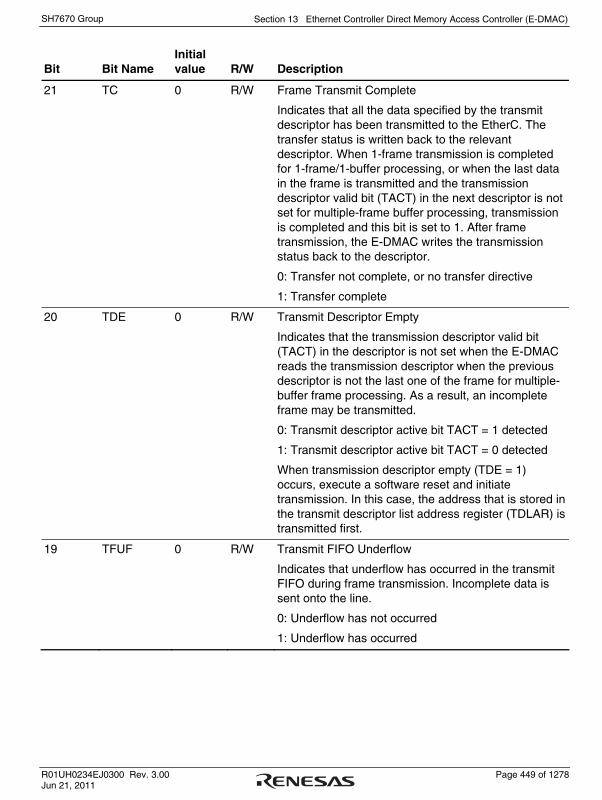
Section 13 Ethernet Controller Direct Memory Access Controller (E-DMAC)
R01UH0234EJ0300 Rev. 3.00 Page 449 of 1278 Jun 21, 2011
SH7670 Group
Bit Bit Name Initial value R/W Description
21 TC 0 R/W Frame Transmit Complete
Indicates that all the data specified by the transmit descriptor has been transmitted to the EtherC. The transfer status is written back to the relevant descriptor. When 1-frame transmission is completed for 1-frame/1-buffer processing, or when the last data in the frame is transmitted and the transmission descriptor valid bit (TACT) in the next descriptor is not set for multiple-frame buffer processing, transmission is completed and this bit is set to 1. After frame transmission, the E-DMAC writes the transmission status back to the descriptor.
0: Transfer not complete, or no transfer directive
1: Transfer complete
20 TDE 0 R/W Transmit Descriptor Empty
Indicates that the transmission descriptor valid bit (TACT) in the descriptor is not set when the E-DMAC reads the transmission descriptor when the previous descriptor is not the last one of the frame for multiple- buffer frame processing. As a result, an incomplete frame may be transmitted.
0: Transmit descriptor active bit TACT = 1 detected
1: Transmit descriptor active bit TACT = 0 detected
When transmission descriptor empty (TDE = 1) occurs, execute a software reset and initiate transmission. In this case, the address that is stored in the transmit descriptor list address register (TDLAR) is transmitted first.
19 TFUF 0 R/W Transmit FIFO Underflow
Indicates that underflow has occurred in the transmit FIFO during frame transmission. Incomplete data is sent onto the line.
0: Underflow has not occurred
1: Underflow has occurred

Section 13 Ethernet Controller Direct Memory Access Controller (E-DMAC)
Page 450 of 1278 R01UH0234EJ0300 Rev. 3.00 Jun 21, 2011
SH7670 Group
Bit Bit Name Initial value R/W Description
18 FR 0 R/W Frame Reception
Indicates that a frame has been received and the receive descriptor has been updated. This bit is set to 1 each time a frame is received.
0: Frame not received
1: Frame received
17 RDE 0 R/W Receive Descriptor Empty
When receive descriptor empty (RDE = 1) occurs, receiving can be restarted by setting RACT = 1 in the receive descriptor and initiating receiving.
0: Receive descriptor active bit RACT = 1 not detected
1: Receive descriptor active bit RACT = 0 detected
16 RFOF 0 R/W Receive FIFO Overflow
Indicates that the receive FIFO has overflowed during frame reception.
0: Overflow has not occurred
1: Overflow has occurred
15 to 12 ⎯ All 0 R Reserved
These bits are always read as 0. The write value should always be 0.
11 CND 0 R/W Carrier Not Detect
Indicates the carrier detection status.
0: A carrier is detected when transmission starts
1: A carrier is not detected when transmission starts
10 DLC 0 R/W Detect Loss of Carrier
Indicates that loss of the carrier has been detected during frame transmission.
0: Loss of carrier not detected
1: Loss of carrier detected
9 CD 0 R/W Delayed Collision Detect
Indicates that a delayed collision has been detected during frame transmission.
0: Delayed collision not detected
1: Delayed collision detected

Section 13 Ethernet Controller Direct Memory Access Controller (E-DMAC)
R01UH0234EJ0300 Rev. 3.00 Page 451 of 1278 Jun 21, 2011
SH7670 Group
Bit Bit Name Initial value R/W Description
8 TRO 0 R/W Transmit Retry Over
Indicates that a retry-over condition has occurred during frame transmission. Total 16 transmission retries including 15 retries based on the back-off algorithm are failed after the EtherC transmission starts.
0: Transmit retry-over condition not detected
1: Transmit retry-over condition detected
7 RMAF 0 R/W Receive Multicast Address Frame
0: Multicast address frame has not been received
1: Multicast address frame has been received
6, 5 ⎯ All 0 R Reserved
These bits are always read as 0. The write value should always be 0.
4 RRF 0 R/W Receive Residual-Bit Frame
0: Residual-bit frame has not been received
1: Residual-bit frame has been received
3 RTLF 0 R/W Receive Too-Long Frame
Indicates that the frame more than the number of receive frame length upper limit set by RFLR of the EtherC has been received.
0: Too-long frame has not been received
1: Too-long frame has been received
2 RTSF 0 R/W Receive Too-Short Frame
Indicates that a frame of fewer than 64 bytes has been received.
0: Too-short frame has not been received
1: Too-short frame has been received
1 PRE 0 R/W PHY Receive Error
0: PHY receive error not detected
1: PHY receive error detected
0 CERF 0 R/W CRC Error on Received Frame
0: CRC error not detected
1: CRC error detected

Section 13 Ethernet Controller Direct Memory Access Controller (E-DMAC)
Page 452 of 1278 R01UH0234EJ0300 Rev. 3.00 Jun 21, 2011
SH7670 Group
13.2.7 EtherC/E-DMAC Status Interrupt Permission Register (EESIPR)
EESIPR is a 32-bit readable/writable register that enables interrupts corresponding to individual bits in the EtherC/E-DMAC status register (EESR). An interrupt is enabled by writing 1 to the corresponding bit. In the initial state, interrupts are not enabled.
31 30 29 28 27 26 25 24 23 22 21 20 19 18 17 16Bit:
Initial Value:R/W:
Bit:
Initial Value:R/W:
15 14 13 12 11 10 9 8 7 6 5 4 3 2 1 0
0 0 0 0 0 0 0 0 0 0 0 0 0 0 0 0R R/W R R R R/W R/W R/W R/W R R/W R/W R/W R/W R/W R/W
0 0 0 0 0 0 0 0 0 0 0 0 0 0 0 0R R R R R/W R/W R/W R/W R/W R R R/W R/W R/W R/W R/W
TWBIP ⎯⎯ ⎯ ⎯ TABTIP RABTIP RFCOFIP
ADEIP ECIIP TCIP TDEIP TFUFIP FRIP RDEIP RFOFIP
⎯ ⎯ ⎯ ⎯ CNDIP DLCIP CDIP TROIP RMAFIP ⎯ ⎯ RRFIP RTLFIP RTSFIP PREIP CERFIP
Bit Bit Name Initial value R/W Description
31 ⎯ 0 R Reserved
This bit is always read as 0. The write value should always be 0.
30 TWBIP 0 R/W Write-Back Complete Interrupt Permission
0: Write-back complete interrupt is disabled
1: Write-back complete interrupt is enabled
29 to 27 ⎯ All 0 R Reserved
These bits are always read as 0. The write value should always be 0.
26 TABTIP 0 R/W Transmit Abort Detection Interrupt Permission
0: Transmit abort detection interrupt is disabled
1: Transmit abort detection interrupt is enabled
25 RABTIP 0 R/W Receive Abort Detection Interrupt Permission
0: Receive abort detection interrupt is disabled
1: Receive abort detection interrupt is enabled
24 RFCOFIP 0 R/W Receive Frame Counter Overflow Interrupt Permission
0: Receive frame counter overflow interrupt is disabled
1: Receive frame counter overflow interrupt is enabled
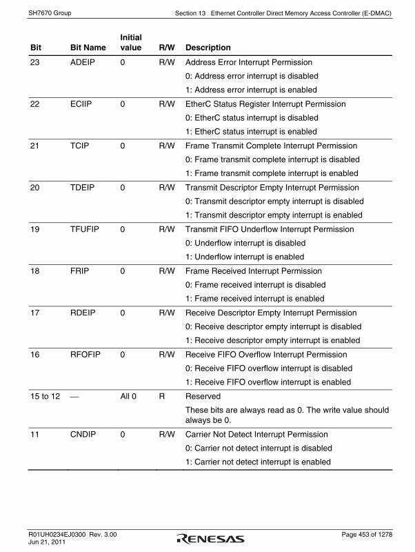
Section 13 Ethernet Controller Direct Memory Access Controller (E-DMAC)
R01UH0234EJ0300 Rev. 3.00 Page 453 of 1278 Jun 21, 2011
SH7670 Group
Bit Bit Name Initial value R/W Description
23 ADEIP 0 R/W Address Error Interrupt Permission
0: Address error interrupt is disabled
1: Address error interrupt is enabled
22 ECIIP 0 R/W EtherC Status Register Interrupt Permission
0: EtherC status interrupt is disabled
1: EtherC status interrupt is enabled
21 TCIP 0 R/W Frame Transmit Complete Interrupt Permission
0: Frame transmit complete interrupt is disabled
1: Frame transmit complete interrupt is enabled
20 TDEIP 0 R/W Transmit Descriptor Empty Interrupt Permission
0: Transmit descriptor empty interrupt is disabled
1: Transmit descriptor empty interrupt is enabled
19 TFUFIP 0 R/W Transmit FIFO Underflow Interrupt Permission
0: Underflow interrupt is disabled
1: Underflow interrupt is enabled
18 FRIP 0 R/W Frame Received Interrupt Permission
0: Frame received interrupt is disabled
1: Frame received interrupt is enabled
17 RDEIP 0 R/W Receive Descriptor Empty Interrupt Permission
0: Receive descriptor empty interrupt is disabled
1: Receive descriptor empty interrupt is enabled
16 RFOFIP 0 R/W Receive FIFO Overflow Interrupt Permission
0: Receive FIFO overflow interrupt is disabled
1: Receive FIFO overflow interrupt is enabled
15 to 12 ⎯ All 0 R Reserved
These bits are always read as 0. The write value should always be 0.
11 CNDIP 0 R/W Carrier Not Detect Interrupt Permission
0: Carrier not detect interrupt is disabled
1: Carrier not detect interrupt is enabled
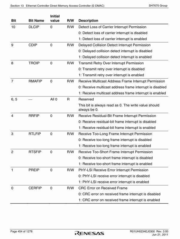
Section 13 Ethernet Controller Direct Memory Access Controller (E-DMAC)
Page 454 of 1278 R01UH0234EJ0300 Rev. 3.00 Jun 21, 2011
SH7670 Group
Bit Bit Name Initial value R/W Description
10 DLCIP 0 R/W Detect Loss of Carrier Interrupt Permission
0: Detect loss of carrier interrupt is disabled
1: Detect loss of carrier interrupt is enabled
9 CDIP 0 R/W Delayed Collision Detect Interrupt Permission
0: Delayed collision detect interrupt is disabled
1: Delayed collision detect interrupt is enabled
8 TROIP 0 R/W Transmit Retry Over Interrupt Permission
0: Transmit retry over interrupt is disabled
1: Transmit retry over interrupt is enabled
7 RMAFIP 0 R/W Receive Multicast Address Frame Interrupt Permission
0: Receive multicast address frame interrupt is disabled
1: Receive multicast address frame interrupt is enabled
6, 5 ⎯ All 0 R Reserved
This bit is always read as 0. The write value should always be 0.
4 RRFIP 0 R/W Receive Residual-Bit Frame Interrupt Permission
0: Receive residual-bit frame interrupt is disabled
1: Receive residual-bit frame interrupt is enabled
3 RTLFIP 0 R/W Receive Too-Long Frame Interrupt Permission
0: Receive too-long frame interrupt is disabled
1: Receive too-long frame interrupt is enabled
2 RTSFIP 0 R/W Receive Too-Short Frame Interrupt Permission
0: Receive too-short frame interrupt is disabled
1: Receive too-short frame interrupt is enabled
1 PREIP 0 R/W PHY-LSI Receive Error Interrupt Permission
0: PHY-LSI receive error interrupt is disabled
1: PHY-LSI receive error interrupt is enabled
0 CERFIP 0 R/W CRC Error on Received Frame
0: CRC error on received frame interrupt is disabled
1: CRC error on received frame interrupt is enabled

Section 13 Ethernet Controller Direct Memory Access Controller (E-DMAC)
R01UH0234EJ0300 Rev. 3.00 Page 455 of 1278 Jun 21, 2011
SH7670 Group
13.2.8 Transmit/Receive Status Copy Enable Register (TRSCER)
TRSCER specifies whether or not transmit and receive status information reported by bits in the EtherC/E-DMAC status register is to be indicated in bits TFS26 to TFS0 and RFS26 to RFS0 in the corresponding descriptor. Bits in this register correspond to bits 11 to 0 in the EtherC/E-DMAC status register (EESR). When a bit is cleared to 0, the transmit status (bits 11 to 8 in EESR) is indicated in bits TFS3 to TFS0 in the transmit descriptor, and the receive status (bits 7 to 0 in EESR) is indicated in bits RFS7 to RFS0 of the receive descriptor. When a bit is set to 1, the occurrence of the corresponding interrupt is not indicated in the descriptor. After this LSI is reset, all bits are cleared to 0.
31 30 29 28 27 26 25 24 23 22 21 20 19 18 17 16Bit:
Initial Value:R/W:
Bit:
Initial Value:R/W:
15 14 13 12 11 10 9 8 7 6 5 4 3 2 1 0
0 0 0 0 0 0 0 0 0 0 0 0 0 0 0 0R R R R R R R R R R R R R R R R
0 0 0 0 0 0 0 0 0 0 0 0 0 0 0 0R R R R R/W R/W R/W R/W R/W R R R/W R/W R/W R/W R/W
⎯ ⎯ ⎯ ⎯ ⎯ ⎯ ⎯ ⎯ ⎯ ⎯ ⎯ ⎯ ⎯ ⎯ ⎯ ⎯
⎯ ⎯ ⎯ ⎯ CNDCE DLCCE CDCE TROCE RMAFCE
⎯ ⎯ RRFCE RTLFCE
RTSFCE
PRECE CERFCE
Bit Bit Name Initial value R/W Description
31 to 12 ⎯ All 0 R Reserved
These bits are always read as 0. The write value should always be 0.
11 CNDCE 0 R/W CND Bit Copy Directive
0: Indicates the CND bit state in bit TFS3 in the transmit descriptor
1: Occurrence of the corresponding interrupt is not indicated in bit TFS3 of the transmit descriptor
10 DLCCE 0 R/W DLC Bit Copy Directive
0: Indicates the DLC bit state in bit TFS2 of the transmit descriptor
1: Occurrence of the corresponding interrupt is not indicated in bit TFS2 of the transmit descriptor
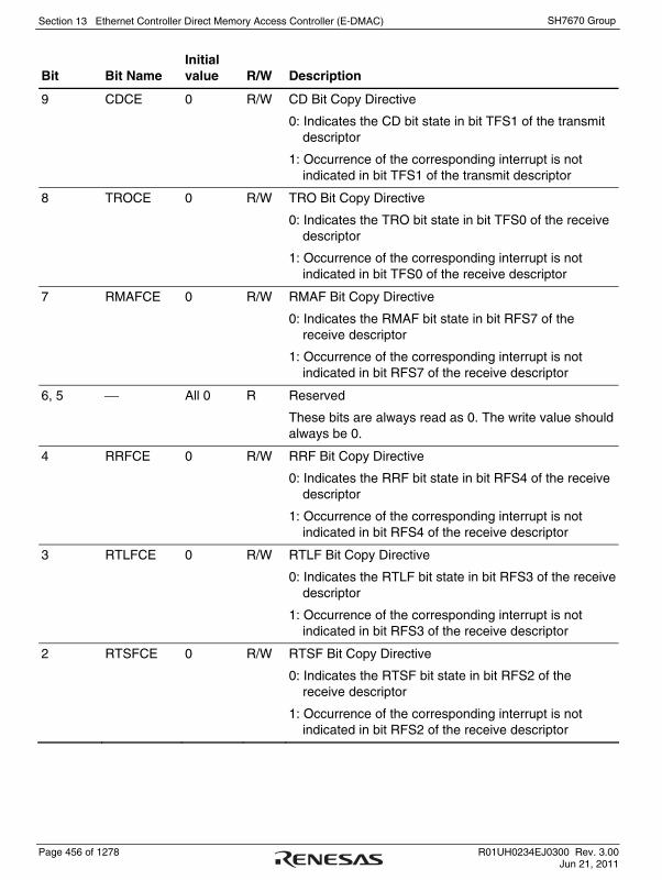
Section 13 Ethernet Controller Direct Memory Access Controller (E-DMAC)
Page 456 of 1278 R01UH0234EJ0300 Rev. 3.00 Jun 21, 2011
SH7670 Group
Bit Bit Name Initial value R/W Description
9 CDCE 0 R/W CD Bit Copy Directive
0: Indicates the CD bit state in bit TFS1 of the transmit descriptor
1: Occurrence of the corresponding interrupt is not indicated in bit TFS1 of the transmit descriptor
8 TROCE 0 R/W TRO Bit Copy Directive
0: Indicates the TRO bit state in bit TFS0 of the receive descriptor
1: Occurrence of the corresponding interrupt is not indicated in bit TFS0 of the receive descriptor
7 RMAFCE 0 R/W RMAF Bit Copy Directive
0: Indicates the RMAF bit state in bit RFS7 of the receive descriptor
1: Occurrence of the corresponding interrupt is not indicated in bit RFS7 of the receive descriptor
6, 5 ⎯ All 0 R Reserved
These bits are always read as 0. The write value should always be 0.
4 RRFCE 0 R/W RRF Bit Copy Directive
0: Indicates the RRF bit state in bit RFS4 of the receive descriptor
1: Occurrence of the corresponding interrupt is not indicated in bit RFS4 of the receive descriptor
3 RTLFCE 0 R/W RTLF Bit Copy Directive
0: Indicates the RTLF bit state in bit RFS3 of the receive descriptor
1: Occurrence of the corresponding interrupt is not indicated in bit RFS3 of the receive descriptor
2 RTSFCE 0 R/W RTSF Bit Copy Directive
0: Indicates the RTSF bit state in bit RFS2 of the receive descriptor
1: Occurrence of the corresponding interrupt is not indicated in bit RFS2 of the receive descriptor

Section 13 Ethernet Controller Direct Memory Access Controller (E-DMAC)
R01UH0234EJ0300 Rev. 3.00 Page 457 of 1278 Jun 21, 2011
SH7670 Group
Bit Bit Name Initial value R/W Description
1 PRECE 0 R/W PRE Bit Copy Directive
0: Indicates the PRF bit state in bit RFS1 of the receive descriptor
1: Occurrence of the corresponding interrupt is not indicated in bit RFS1 of the receive descriptor
0 CERFCE 0 R/W CERF Bit Copy Directive
0: Indicates the CERF bit state in bit RFS0 of the receive descriptor
1: Occurrence of the corresponding interrupt is not indicated in bit RFS0 of the receive descriptor
13.2.9 Receive Missed-Frame Counter Register (RMFCR)
RMFCR is a 16-bit counter that indicates the number of frames missed (discarded, and not transferred to the receive buffer) during reception. When the receive FIFO overflows, the receive frames in the FIFO are discarded. The number of frames discarded at this time is counted. When the value in this register reaches H'FFFF, counting-up is halted. When this register is read, the counter value is cleared to 0. Write operations to this register have no effect.
31 30 29 28 27 26 25 24 23 22 21 20 19 18 17 16Bit:
Initial Value:R/W:
Bit:
Initial Value:R/W:
15 14 13 12 11 10 9 8 7 6 5 4 3 2 1 0
0 0 0 0 0 0 0 0 0 0 0 0 0 0 0 0R R R R R R R R R R R R R R R R
0 0 0 0 0 0 0 0 0 0 0 0 0 0 0 0R R R R R R R R R R R R R R R R
⎯ ⎯ ⎯ ⎯ ⎯ ⎯ ⎯ ⎯ ⎯ ⎯ ⎯ ⎯ ⎯ ⎯ ⎯ ⎯
MFC[15:0]
Bit Bit Name Initial value R/W Description
31 to 16 ⎯ All 0 R Reserved
These bits are always read as 0. The write value should always be 0.
15 to 0 MFC[15:0] All 0 R Missed-Frame Counter
Indicate the number of frames that are discarded and not transferred to the receive buffer during reception.

Section 13 Ethernet Controller Direct Memory Access Controller (E-DMAC)
Page 458 of 1278 R01UH0234EJ0300 Rev. 3.00 Jun 21, 2011
SH7670 Group
13.2.10 Transmit FIFO Threshold Register (TFTR)
TFTR is a 32-bit readable/writable register that specifies the transmit FIFO threshold at which the first transmission is started. The actual threshold is 4 times the set value. The EtherC starts transmission when the amount of data in the transmit FIFO exceeds the number of bytes specified by this register, when the transmit FIFO is full, or when 1-frame write is executed. When setting this register, do so in the transmission-halt state.
31 30 29 28 27 26 25 24 23 22 21 20 19 18 17 16Bit:
Initial Value:R/W:
Bit:
Initial Value:R/W:
15 14 13 12 11 10 9 8 7 6 5 4 3 2 1 0
0 0 0 0 0 0 0 0 0 0 0 0 0 0 0 0R R R R R R R R R R R R R R R R
0 0 0 0 0 0 0 0 0 0 0 0 0 0 0 0R R R R R R/W R/W R/W R/W R/W R/W R/W R/W R/W R/W R/W
⎯ ⎯ ⎯ ⎯ ⎯
⎯ ⎯ ⎯ ⎯ ⎯
⎯ ⎯ ⎯ ⎯ ⎯ ⎯ ⎯ ⎯ ⎯ ⎯ ⎯
TFT[10:0]
Bit Bit Name Initial value R/W Description
31 to 11 ⎯ All 0 R Reserved
These bits are always read as 0. The write value should always be 0.
10 to 0 TFT[10:0] All 0 R/W Transmit FIFO threshold
When setting a transmit FIFO, the FIFO must be set to a smaller value than the specified value of the FIFO capacity by FDR. H'00: Store and forward modes H'01 to H'0C: Setting prohibited
H'0D: 52 bytes
H'0E: 56 bytes : : H'1F: 124 bytes
H'20: 128 bytes : : H'3F: 252 bytes
H'40: 256 bytes : : H'7F: 508 bytes
H'80: 512 bytes H'81 to H'200: Setting prohibited
Note: When starting transmission before one frame of data write has completed, take care the generation of the underflow.

Section 13 Ethernet Controller Direct Memory Access Controller (E-DMAC)
R01UH0234EJ0300 Rev. 3.00 Page 459 of 1278 Jun 21, 2011
SH7670 Group
13.2.11 FIFO Depth Register (FDR)
FDR is a 32-bit readable/writable register that specifies the depth of the transmit and receive FIFOs.
31 30 29 28 27 26 25 24 23 22 21 20 19 18 17 16
15 14 13 12 11 10 9 8 7 6 5 4 3 2 1 0
0 0 0 0 0 0 0 0 0 0 0 0 0 0 0 0R R R R R R R R R R R R R R R R
0 0 0 0 0 0 0 1 0 0 0 0 0 0 0 1R R R R R R/W R/W R/W R R R R R R/W R/W R/W
⎯ ⎯ ⎯ ⎯ ⎯ ⎯ ⎯ ⎯ ⎯ ⎯ ⎯ ⎯ ⎯ ⎯ ⎯ ⎯
⎯ ⎯ ⎯ ⎯ ⎯ TFD2 TFD1 TFD0 ⎯ ⎯ ⎯ ⎯ ⎯ RFD2 RFD1 RFD0
Bit:
Initial Value:R/W:
Bit:
Initial Value:R/W:
Bit Bit Name Initial value R/W Description
31 to 11 ⎯ All 0 R Reserved
These bits are always read as 0. The write value should always be 0.
10
9
8
TFD2
TFD1
TFD0
0
0
1
R/W
R/W
R/W
Transmit FIFO Depth
These bits specify the depth of the transmit FIFO. After the start of the transmission and reception, the setting cannot be changed.
000: 256 bytes
001: 512 bytes
Other than above: Setting prohibited
7 to 3 ⎯ All 0 R Reserved
These bits are always read as 0. The write value should always be 0.
2
1
0
RFD2
RFD1
RFD0
0
0
1
R/W
R/W
R/W
Receive FIFO Depth
These bits specify the depth of the receive FIFO. After the start of the transmission and reception, the setting cannot be changed.
000: 256 bytes
001: 512 bytes
Other than above: Setting prohibited
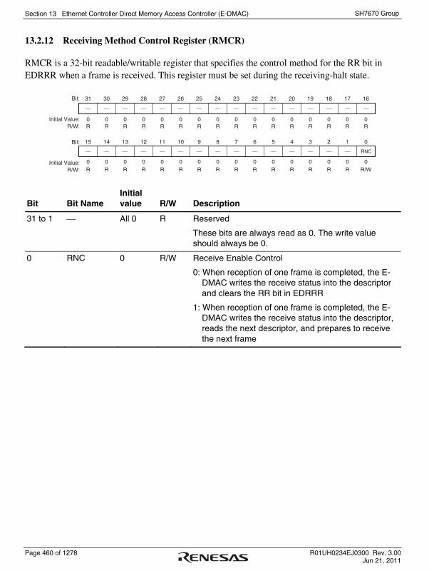
Section 13 Ethernet Controller Direct Memory Access Controller (E-DMAC)
Page 460 of 1278 R01UH0234EJ0300 Rev. 3.00 Jun 21, 2011
SH7670 Group
13.2.12 Receiving Method Control Register (RMCR)
RMCR is a 32-bit readable/writable register that specifies the control method for the RR bit in EDRRR when a frame is received. This register must be set during the receiving-halt state.
31 30 29 28 27 26 25 24 23 22 21 20 19 18 17 16Bit:
Initial Value:R/W:
Bit:
Initial Value:R/W:
15 14 13 12 11 10 9 8 7 6 5 4 3 2 1 0
0 0 0 0 0 0 0 0 0 0 0 0 0 0 0 0R R R R R R R R R R R R R R R R
0 0 0 0 0 0 0 0 0 0 0 0 0 0 0 0R R R R R R R R R R R R R R R R/W
⎯ ⎯ ⎯ ⎯ ⎯ ⎯ ⎯ ⎯ ⎯ ⎯ ⎯ ⎯ ⎯ ⎯ ⎯ ⎯
⎯ ⎯ ⎯ ⎯ ⎯ ⎯ ⎯ ⎯ ⎯ ⎯ ⎯ ⎯ ⎯ ⎯ ⎯ RNC
Bit Bit Name Initial value R/W Description
31 to 1 ⎯ All 0 R Reserved
These bits are always read as 0. The write value should always be 0.
0 RNC 0 R/W Receive Enable Control
0: When reception of one frame is completed, the E-DMAC writes the receive status into the descriptor and clears the RR bit in EDRRR
1: When reception of one frame is completed, the E-DMAC writes the receive status into the descriptor, reads the next descriptor, and prepares to receive the next frame

Section 13 Ethernet Controller Direct Memory Access Controller (E-DMAC)
R01UH0234EJ0300 Rev. 3.00 Page 461 of 1278 Jun 21, 2011
SH7670 Group
13.2.13 E-DMAC Operation Control Register (EDOCR)
EDOCR is a 32-bit readable/writable register that specifies the control methods used in E-DMAC operation.
31 30 29 28 27 26 25 24 23 22 21 20 19 18 17 16Bit:
Initial Value:R/W:
Bit:
Initial Value:R/W:
15 14 13 12 11 10 9 8 7 6 5 4 3 2 1 0
0 0 0 0 0 0 0 0 0 0 0 0 0 0 0 0R R R R R R R R R R R R R R R R
0 0 0 0 0 0 0 0 0 0 0 0 0 0 0 0R R R R R R R R R R R R R/W R/W R/W R
⎯ ⎯ ⎯ ⎯ ⎯ ⎯ ⎯ ⎯ ⎯ ⎯ ⎯ ⎯ ⎯ ⎯ ⎯ ⎯
⎯ ⎯ ⎯ ⎯ ⎯ ⎯ ⎯ ⎯ ⎯ ⎯ ⎯ ⎯ FEC AEC EDH ⎯
Bit Bit Name Initial value R/W Description
31 to 4 ⎯ All 0 R Reserved
These bits are always read as 0. The write value should always be 0.
3 FEC 0 R/W FIFO Error Control
Specifies E-DMAC operation when transmit FIFO underflow or receive FIFO overflow occurs.
0: E-DMAC operation continues when underflow or overflow occurs
1: E-DMAC operation halts when underflow or overflow occurs
2 AEC 0 R/W Address Error Control
Indicates detection of an illegal memory address in an attempted E-DMAC transfer.
0: Illegal memory address not detected (normal operation)
1: E-DMAC stops its operation due to illegal memory address detection
Note: To resume the operation, set the E-DMAC again after software reset by means of the SWR bit in EDMR.

Section 13 Ethernet Controller Direct Memory Access Controller (E-DMAC)
Page 462 of 1278 R01UH0234EJ0300 Rev. 3.00 Jun 21, 2011
SH7670 Group
Bit Bit Name Initial value R/W Description
1 EDH 0 R/W E-DMAC Halted
0: The E-DMAC is operating normally
1: The E-DMAC has been halted by NMI pin assertion. E-DMAC operation is restarted by writing 0
0 ⎯ 0 R Reserved
This bit is always read as 0. The write value should always be 0.
13.2.14 Receiving-Buffer Write Address Register (RBWAR)
RBWAR stores the address of data to be written in the receiving buffer when the E-DMAC writes data to the receiving buffer. Which addresses in the receiving buffer are processed by the E-DMAC can be recognized by monitoring addresses displayed in this register. The address that the E-DMAC is actually processing may be different from the value read from this register.
31 30 29 28 27 26 25 24 23 22 21 20 19 18 17 16Bit:
Initial Value:R/W:
Bit:
Initial Value:R/W:
15 14 13 12 11 10 9 8 7 6 5 4 3 2 1 0
0 0 0 0 0 0 0 0 0 0 0 0 0 0 0 0R R R R R R R R R R R R R R R R
0 0 0 0 0 0 0 0 0 0 0 0 0 0 0 0R R R R R R R R R R R R R R R R
RBWA[31:16]
RBWA[15:0]
Bit Bit Name Initial value R/W Description
31 to 0 RBWA[31:0] All 0 R Receiving-Buffer Write Address
These bits can only be read. Writing is prohibited.

Section 13 Ethernet Controller Direct Memory Access Controller (E-DMAC)
R01UH0234EJ0300 Rev. 3.00 Page 463 of 1278 Jun 21, 2011
SH7670 Group
13.2.15 Receiving-Descriptor Fetch Address Register (RDFAR)
RDFAR stores the descriptor start address that is required when the E-DMAC fetches descriptor information from the receiving descriptor. Which receiving descriptor information is used for processing by the E-DMAC can be recognized by monitoring addresses displayed in this register. The address from which the E-DMAC is actually fetching a descriptor may be different from the value read from this register.
31 30 29 28 27 26 25 24 23 22 21 20 19 18 17 16Bit:
Initial Value:R/W:
Bit:
Initial Value:R/W:
15 14 13 12 11 10 9 8 7 6 5 4 3 2 1 0
0 0 0 0 0 0 0 0 0 0 0 0 0 0 0 0
0 0 0 0 0 0 0 0 0 0 0 0 0 0 0 0
RDFA[31:16]
R R R R R R R R R R R R R R R R
R R R R R R R R R R R R R R R R
RDFA[15:0]
Bit Bit Name Initial value R/W Description
31 to 0 RDFA[31:0] All 0 R Receiving-Descriptor Fetch Address
These bits can only be read. Writing is prohibited.
13.2.16 Transmission-Buffer Read Address Register (TBRAR)
TBRAR stores the address of the transmission buffer when the E-DMAC reads data from the transmission buffer. Which addresses in the transmission buffer are processed by the E-DMAC can be recognized by monitoring addresses displayed in this register. The address from which the E-DMAC is actually reading in the buffer may be different from the value read from this register.
31 30 29 28 27 26 25 24 23 22 21 20 19 18 17 16Bit:
Initial Value:R/W:
15 14 13 12 11 10 9 8 7 6 5 4 3 2 1 0Bit:
Initial Value:R/W:
0 0 0 0 0 0 0 0 0 0 0 0 0 0 0 0
0 0 0 0 0 0 0 0 0 0 0 0 0 0 0 0
TBRA[31:16]
R R R R R R R R R R R R R R R R
R R R R R R R R R R R R R R R R
TBRA[15:0]
Bit Bit Name Initial value R/W Description
31 to 0 TBRA[31:0] All 0 R Transmission-Buffer Read Address
These bits can only be read. Writing is prohibited.

Section 13 Ethernet Controller Direct Memory Access Controller (E-DMAC)
Page 464 of 1278 R01UH0234EJ0300 Rev. 3.00 Jun 21, 2011
SH7670 Group
13.2.17 Transmission-Descriptor Fetch Address Register (TDFAR)
TDFAR stores the descriptor start address that is required when the E-DMAC fetches descriptor information from the transmission descriptor. Which transmission descriptor information is used for processing by the E-DMAC can be recognized by monitoring addresses displayed in this register. The address from which the E-DMAC is actually fetching a descriptor may be different from the value read from this register.
31 30 29 28 27 26 25 24 23 22 21 20 19 18 17 16Bit:
Initial Value:R/W:
15 14 13 12 11 10 9 8 7 6 5 4 3 2 1 0Bit:
Initial Value:R/W:
0 0 0 0 0 0 0 0 0 0 0 0 0 0 0 0
0 0 0 0 0 0 0 0 0 0 0 0 0 0 0 0
TDFA[31:16]
R R R R R R R R R R R R R R R R
R R R R R R R R R R R R R R R R
TDFA[15:0]
Bit Bit Name Initial value R/W Description
31 to 0 TDFA[31:0] All 0 R Transmission-Descriptor Fetch Address
These bits can only be read. Writing is prohibited.
13.2.18 Flow Control FIFO Threshold Register (FCFTR)
FCFTR is a 32-bit readable/writable register that sets the flow control of the EtherC (setting the threshold on automatic PAUSE transmission). The threshold can be specified by the depth of the receive FIFO data (RFD2 to RFD0) and the number of receive frames (RFF2 to RFF0). The condition to start the flow control is decided by taking OR operation on the two thresholds. Therefore, the flow control by the two thresholds is independently started.
When flow control is performed according to the RFD bits setting, if the setting is the same as the depth of the receive FIFO specified by the FIFO depth register (FDR), flow control is started when the remaining FIFO is (FIFO data − 64) bytes. For instance, when RFD in FDR = 1 and RFD in FCFTR = 1, flow control is started when (512 − 64) bytes of data is stored in the receive FIFO. The value set in the RFD bits in this register should be equal to or less than those in FDR.

Section 13 Ethernet Controller Direct Memory Access Controller (E-DMAC)
R01UH0234EJ0300 Rev. 3.00 Page 465 of 1278 Jun 21, 2011
SH7670 Group
31 30 29 28 27 26 25 24 23 22 21 20 19 18 17 16
15 14 13 12 11 10 9 8 7 6 5 4 3 2 1 0
0 0 0 0 0 0 0 0 0 0 0 0 0 1 1 1R R R R R R R R R R R R R R/W R/W R/W
0 0 0 0 0 0 0 0 0 0 0 0 0 0 0 0R R R R R R R R R R R R R R/W R/W R/W
⎯ ⎯ ⎯ ⎯ ⎯ ⎯ ⎯ ⎯ ⎯ ⎯ ⎯ ⎯ ⎯ RFF[2:0]
⎯ ⎯ ⎯ ⎯ ⎯ ⎯ ⎯ ⎯ ⎯ ⎯ ⎯ ⎯ ⎯ RFD[2:0]
Bit:
Initial Value:R/W:
Bit:
Initial Value:R/W:
Bit Bit Name Initial value R/W Description
31 to 19 ⎯ All 0 R Reserved
These bits are always read as 0. The write value should always be 0.
18 to 16 RFF[2:0] 111 R/W Receive Frame Number Flow Control Threshold
000: When one receive frame has been stored in the receive FIFO
001: When two receive frames have been stored in the receive FIFO
: :
110: When seven receive frames have been stored in the receive FIFO
111: When eight receive frames have been stored in the receive FIFO
15 to 3 ⎯ All 0 ⎯ Reserved
These bits are always read as 0. The write value should always be 0.
2 to 0 RFD[2:0] 000 R/W Receive Byte Flow Control Threshold
000: When (256 − 64) bytes of data is stored in the receive FIFO
001: When (512 − 64) bytes of data is stored in the receive FIFO
Other than above: Setting prohibited

Section 13 Ethernet Controller Direct Memory Access Controller (E-DMAC)
Page 466 of 1278 R01UH0234EJ0300 Rev. 3.00 Jun 21, 2011
SH7670 Group
13.2.19 Receive Data Padding Setting Register (RPADIR)
RPADIR is a 32-bit readable/writable register that performs the padding of receive data. Before setting this register again, reset the software with the SWR bit in the E-DMAC mode register (EDMR).
31 30 29 28 27 26 25 24 23 22 21 20 19 18 17 16Bit:
Initial Value:R/W:
Bit:
Initial Value:R/W:
15 14 13 12 11 10 9 8 7 6 5 4 3 2 1 0
0 0 0 0 0 0 0 0 0 0 0 0 0 0 0 0R R R R R R R R R R R R R R R/W R/W
0 0 0 0 0 0 0 0 0 0 0 0 0 0 0 0R R R R R R R R R R R/W R/W R/W R/W R/W R/W
⎯ ⎯ ⎯ ⎯ ⎯ ⎯ ⎯ ⎯ ⎯ ⎯ ⎯ ⎯ ⎯ ⎯ PADS1 PADS0
⎯ ⎯ ⎯ ⎯ ⎯ ⎯ ⎯ ⎯ ⎯ ⎯ PADR[5:0]
Bit Bit Name Initial value R/W Description
31 to 18 ⎯ All 0 ⎯ Reserved
These bits are always read as 0. The write value should always be 0.
17
16
PADS1
PADS0
0
0
R/W
R/W
Padding size
00: No padding
01: Padding of one byte
10: Padding of two bytes
11: Padding of three bytes
15 to 6 ⎯ All 0 ⎯ Reserved
These bits are always read as 0. The write value should always be 0.
5 to 0 PADR[5:0] 000000 R/W Padding Range
H'00: Data equivalent to the padding size is inserted in the first byte.
H'01: Data equivalent to the padding size is inserted in the second byte.
: :
H'3E: Data equivalent to the padding size is inserted in the 63rd byte.
H'3F: Data equivalent to the padding size is inserted in the 64th byte.

Section 13 Ethernet Controller Direct Memory Access Controller (E-DMAC)
R01UH0234EJ0300 Rev. 3.00 Page 467 of 1278 Jun 21, 2011
SH7670 Group
13.2.20 Transmit Interrupt Register (TRIMD)
TRIMD is a 32-bit readable/writable register that specifies whether or not to notify write-back completion for each frame using the TWB bit in EESR and an interrupt on transmit operations.
31 30 29 28 27 26 25 24 23 22 21 20 19 18 17 16Bit:
Initial Value:R/W:
Bit:
Initial Value:R/W:
15 14 13 12 11 10 9 8 7 6 5 4 3 2 1 0
0 0 0 0 0 0 0 0 0 0 0 0 0 0 0 0R R R R R R R R R R R R R R R R
0 0 0 0 0 0 0 0 0 0 0 0 0 0 0 0R R R R R R R R R R R R R R R R/W
⎯ ⎯ ⎯ ⎯ ⎯ ⎯ ⎯ ⎯ ⎯ ⎯ ⎯ ⎯ ⎯ ⎯ ⎯ ⎯
⎯ ⎯ ⎯ ⎯ ⎯ ⎯ ⎯ ⎯ ⎯ ⎯ ⎯ ⎯ ⎯ ⎯ ⎯ TIS
Bit Bit Name Initial value R/W Description
31 to 1 ⎯ All 0 R Reserved
These bits are always read as 0. The write value should always be 0.
0 TIS 0 R/W Transmit Interrupt Setting
0: Write-back completion for each frame is not notified
1: Write-backed completion for each frame using the TWB bit in EESR is notified
13.2.21 Checksum Mode Register (CSMR)
CSMR is a 32-bit readable/writable register that specifies the checksum operating mode. Set this register when reception is stopped.
31 30 29 28 27 26 25 24 23 22 21 20 19 18 17 16Bit:
Initial Value:R/W:
15 14 13 12 11 10 9 8 7 6 5 4 3 2 1 0
1 1 0 0 0 0 0 0 0 0 0 0 0 0 0 0R/W R/W R R R R R R R R R R R R R R
0 0 0 0 0 0 0 0 0 0 0 1 1 0 1 0R R R R R R R R R R R/W R/W R/W R/W R/W R/W
CSEBL CSMD ⎯ ⎯ ⎯ ⎯ ⎯ ⎯ ⎯ ⎯ ⎯ ⎯ ⎯ ⎯ ⎯ ⎯
⎯ ⎯ ⎯ ⎯ ⎯ ⎯ ⎯ ⎯ ⎯ ⎯ SB[5:0]

Section 13 Ethernet Controller Direct Memory Access Controller (E-DMAC)
Page 468 of 1278 R01UH0234EJ0300 Rev. 3.00 Jun 21, 2011
SH7670 Group
Bit Bit Name Initial value R/W Description
31 CSEBL 1 R/W Operation Setting for Checksum Calculation Function
0: The result of checksum calculation is not written
back to the receive descriptor.
1: The result of checksum calculation is written back
to the receive descriptor.
30 CSMD 1 R/W Setting for Checksum Calculation Mode
0: Checksums are calculated on all the remaining
data after skipping the number of bytes specified in
SB5 to SB0 from the beginning of the MAC layer
packet.
1: Packet checksums for the upper layer such as TCP
or UDP are calculated along with the analysis of
the MAC/IP layer packet.
29 to 6 ⎯ All 0 R Reserved
These bits are always read as 0. The write value should always be 0.
5 to 0 SB[5:0]* 011010 R/W Bytes Skipped in Checksum Calculation
These bits specify the number of bytes to be skipped from the beginning of a receive MAC packet.
H'00: Byte 0 (checksum calculation starts from the beginning of a receive MAC packet)
H'02: Byte 2
: :
H'1A: Byte 26
: :
H'3E: Byte 62
Note * Setting is possible only when CSEBL = 1 and CSMD = 0. Otherwise, 6'h00 should be set.

Section 13 Ethernet Controller Direct Memory Access Controller (E-DMAC)
R01UH0234EJ0300 Rev. 3.00 Page 469 of 1278 Jun 21, 2011
SH7670 Group
13.2.22 Checksum Skipped Bytes Monitor Register (CSSBM )
CSSBM is a 32-bit read-only register that stores the number of skipped bytes during the processing of received packets in the E-DMAC. The number of skipped bytes can be recognized by monitoring the value displayed by this register. Note that the number of items of data received by the E-DMAC may be different from the number of skipped bytes.
31 30 29 28 27 26 25 24 23 22 21 20 19 18 17 16Bit:
Initial Value:R/W:
Bit:
Initial Value:R/W:
15 14 13 12 11 10 9 8 7 6 5 4 3 2 1 0
0 0 0 0 0 0 0 0 0 0 0 0 0 0 0 0R R R R R R R R R R R R R R R R
0 0 0 0 0 0 0 0 0 0 0 0 0 0 0 0R R R R R R R R R R R R R R R R
⎯ ⎯ ⎯ ⎯ ⎯ ⎯ ⎯ ⎯ ⎯ ⎯ ⎯ ⎯ ⎯ ⎯ ⎯ ⎯
⎯ ⎯ ⎯ ⎯ ⎯ ⎯ ⎯ ⎯ ⎯ ⎯ SBM[5:0]
Bit Bit Name Initial value R/W Description
31 to 6 ⎯ All 0 R Reserved
These bits are always read as 0. The write value should always be 0.
5 to 0 SBM[5:0] 000000 R/W Number of Skipped Bytes
These bits can only be read. Writing is prohibited.
These bits are initialized to 0 at the beginning of a receive packet.
Note * The value is valid only when CSEBL = 1 and CSMD = 0.

Section 13 Ethernet Controller Direct Memory Access Controller (E-DMAC)
Page 470 of 1278 R01UH0234EJ0300 Rev. 3.00 Jun 21, 2011
SH7670 Group
13.2.23 Checksum Monitor Register (CSSMR)
CSSMR is a 32-bit read-only register that stores the value of a checksum during the processing of received packets in E-DMAC. The checksum value can be recognized by monitoring the value displayed by this register. Note that the value of the data received by E-DMAC may be different from the checksum value.
31 30 29 28 27 26 25 24 23 22 21 20 19 18 17 16Bit:
Initial Value:R/W:
Bit:
Initial Value:R/W:
15 14 13 12 11 10 9 8 7 6 5 4 3 2 1 0
0 0 0 0 0 0 0 0 0 0 0 0 0 0 0 0R R R R R R R R R R R R R R R R
0 0 0 0 0 0 0 0 0 0 0 0 0 0 0 0R R R R R R R R R R R R R R R R
⎯ ⎯ ⎯ ⎯ ⎯ ⎯ ⎯ ⎯ ⎯ ⎯ ⎯ ⎯ ⎯ ⎯ ⎯ ⎯
CS[15:0]
Bit Bit Name Initial value R/W Description
31 to 16 ⎯ All 0 R Reserved
These bits are always read as 0. The write value should always be 0.
15 to 0 CS[15:0] 0 R Checksum Value
These bits can only be read. Writing is prohibited.
These bits are initialized to 0 at the beginning of a receive packet.
Note * The value is valid only when CSEBL = 1 and CSMD = 0.

Section 13 Ethernet Controller Direct Memory Access Controller (E-DMAC)
R01UH0234EJ0300 Rev. 3.00 Page 471 of 1278 Jun 21, 2011
SH7670 Group
13.3 Operation
The E-DMAC is connected to the EtherC, and performs efficient transfer of transmit/receive data between the EtherC and memory (buffers) without the intervention of the CPU. The E-DMAC itself reads control information, including buffer pointers called descriptors, relating to the buffers. The E-DMAC reads transmit data from the transmit buffer and writes receive data to the receive buffer in accordance with this control information. By setting up a number of consecutive descriptors (a descriptor list), it is possible to execute transmission and reception continuously.
13.3.1 Descriptor List and Data Buffers
Before starting transmission/reception, the communication program creates transmit and receive descriptor lists in memory. The start addresses of these lists are then set in the transmit and receive descriptor list start address registers.
The descriptor start address must be aligned so that it matches the address boundary according to the descriptor length set by the E-DMAC mode register (EDMR). The transmit buffer start address can be aligned with a byte, a word, and a longword boundary.
(1) Transmit Descriptor
Figure 13.2 shows the relationship between a transmit descriptor and the transmit buffer. According to the specification in this descriptor, the relationship between the transmit frame and transmit buffer can be defined as one frame/one buffer or one frame/multi-buffer.

Section 13 Ethernet Controller Direct Memory Access Controller (E-DMAC)
Page 472 of 1278 R01UH0234EJ0300 Rev. 3.00 Jun 21, 2011
SH7670 Group
Transmit descriptor Transmit buffer
Valid transmit data
TACT
TDLE
TFP1
TFP0
TFS26 to TFS0TD0
TDLTD1
TBA
Padding (4 bytes)
TD2
31 30 29 28 27 26 0TFE
31 16
31 0
Figure 13.2 Relationship between Transmit Descriptor and Transmit Buffer

Section 13 Ethernet Controller Direct Memory Access Controller (E-DMAC)
R01UH0234EJ0300 Rev. 3.00 Page 473 of 1278 Jun 21, 2011
SH7670 Group
(a) Transmit Descriptor 0 (TD0)
TD0 indicates the transmit frame status. The CPU and E-DMAC use TD0 to report the frame transmission status.
31 30 29 28 27 26 25 24 23 22 21 20 19 18 17 16Bit:
Initial Value:R/W:
Bit:
Initial Value:R/W:
15 14 13 12 11 10 9 8 7 6 5 4 3 2 1 0
0 0 0 0 0 0 0 0 0 0 0 0 0 0 0 0R/W R/W R/W R/W R/W R/W R/W R/W R/W R/W R/W R/W R/W R/W R/W R/W
0 0 0 0 0 0 0 0 0 0 0 0 0 0 0 0R/W R/W R/W R/W R/W R/W R/W R/W R/W R/W R/W R/W R/W R/W R/W R/W
TACT TDLE TFP1 TFP0 TFE TFS[26:16]
TFS[15:0]
Bit Bit Name Initial value R/W Description
31 TACT 0 R/W Transmit Descriptor Active
Indicates that this descriptor is active. The CPU sets this bit after transmit data has been transferred to the transmit buffer. The E-DMAC resets this bit on completion of a frame transfer or when transmission is suspended.
0: The transmit descriptor is invalid.
Indicates that valid data has not been written to this bit by the CPU, or this bit has been reset by a write-back operation on termination of E-DMAC frame transfer processing (completion or suspension of transmission)
If this state is recognized in an E-DMAC descriptor read, the E-DMAC terminates transmit processing and transmit operations cannot be continued (a restart is necessary)
1: The transmit descriptor is valid.
Indicates that valid data has been written to the transmit buffer by the CPU and frame transfer processing has not yet been executed, or that frame transfer is in progress
When this state is recognized in an E-DMAC descriptor read, the E-DMAC continues with the transmit operation

Section 13 Ethernet Controller Direct Memory Access Controller (E-DMAC)
Page 474 of 1278 R01UH0234EJ0300 Rev. 3.00 Jun 21, 2011
SH7670 Group
Bit Bit Name Initial value R/W Description
30 TDLE 0 R/W Transmit Descriptor List End
After completion of the corresponding buffer transfer, the E-DMAC references the first descriptor. This specification is used to set a ring configuration for the transmit descriptors.
0: This is not the last transmit descriptor list
1: This is the last transmit descriptor list
29
28
TFP1
TFP0
0
0
R/W
R/W
Transmit Frame Position 1, 0
These two bits specify the relationship between the transmit buffer and transmit frame. In the preceding and following descriptors, a logically positive relationship must be maintained between the settings of this bit and the TDLE bit.
00: Frame transmission for transmit buffer indicated by this descriptor continues (frame is not concluded)
01: Transmit buffer indicated by this descriptor contains end of frame (frame is concluded)
10: Transmit buffer indicated by this descriptor is start of frame (frame is not concluded)
11: Contents of transmit buffer indicated by this descriptor are equivalent to one frame (one frame/one buffer)
27 TFE 0 R/W Transmit Frame Error
Indicates that one or other bit of the transmit frame status indicated by bits 26 to 0 is set. Whether or not the transmit frame status information is copied into this bit is specified by the transmit/receive status copy enable register.
0: No error during transmission
1: An error occurred during transmission
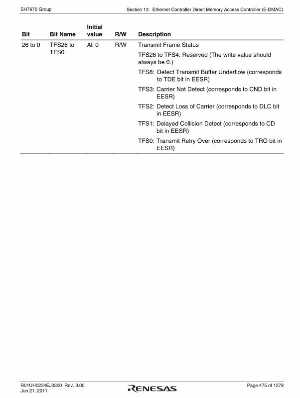
Section 13 Ethernet Controller Direct Memory Access Controller (E-DMAC)
R01UH0234EJ0300 Rev. 3.00 Page 475 of 1278 Jun 21, 2011
SH7670 Group
Bit Bit Name Initial value R/W Description
26 to 0 TFS26 to TFS0
All 0 R/W Transmit Frame Status
TFS26 to TFS4: Reserved (The write value should always be 0.)
TFS8: Detect Transmit Buffer Underflow (corresponds to TDE bit in EESR)
TFS3: Carrier Not Detect (corresponds to CND bit in EESR)
TFS2: Detect Loss of Carrier (corresponds to DLC bit in EESR)
TFS1: Delayed Collision Detect (corresponds to CD bit in EESR)
TFS0: Transmit Retry Over (corresponds to TRO bit in EESR)
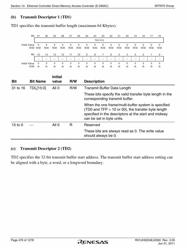
Section 13 Ethernet Controller Direct Memory Access Controller (E-DMAC)
Page 476 of 1278 R01UH0234EJ0300 Rev. 3.00 Jun 21, 2011
SH7670 Group
(b) Transmit Descriptor 1 (TD1)
TD1 specifies the transmit buffer length (maximum 64 Kbytes).
31 30 29 28 27 26 25 24 23 22 21 20 19 18 17 16Bit:
Initial Value:R/W:
Bit:
Initial Value:R/W:
15 14 13 12 11 10 9 8 7 6 5 4 3 2 1 0
0 0 0 0 0 0 0 0 0 0 0 0 0 0 0 0R/W R/W R/W R/W R/W R/W R/W R/W R/W R/W R/W R/W R/W R/W R/W R/W
0 0 0 0 0 0 0 0 0 0 0 0 0 0 0 0R R R R R R R R R R R R R R R R
TDL[15:0]
⎯ ⎯ ⎯ ⎯ ⎯ ⎯ ⎯ ⎯ ⎯ ⎯ ⎯ ⎯ ⎯ ⎯ ⎯ ⎯
Bit Bit Name Initial value R/W Description
31 to 16 TDL[15:0] All 0 R/W Transmit Buffer Data Length
These bits specify the valid transfer byte length in the corresponding transmit buffer.
When the one frame/multi-buffer system is specified (TD0 and TFP = 10 or 00), the transfer byte length specified in the descriptors at the start and midway can be set in byte units.
15 to 0 ⎯ All 0 R Reserved
These bits are always read as 0. The write value should always be 0.
(c) Transmit Descriptor 2 (TD2)
TD2 specifies the 32-bit transmit buffer start address. The transmit buffer start address setting can be aligned with a byte, a word, or a longword boundary.

Section 13 Ethernet Controller Direct Memory Access Controller (E-DMAC)
R01UH0234EJ0300 Rev. 3.00 Page 477 of 1278 Jun 21, 2011
SH7670 Group
(2) Receive Descriptor
Figure 13.3 shows the relationship between a receive descriptor and the receive buffer. In frame reception, the E-DMAC performs data rewriting up to a receive buffer 16-byte boundary, regardless of the receive frame length. Finally, the actual receive frame length is reported in the lower 16 bits of RD1 in the descriptor. Data transfer to the receive buffer is performed automatically by the E-DMAC to give a one frame/one buffer or one frame/multi-buffer configuration according to the size of one received frame.
Receive descriptor Receive buffer
Valid receive data
RFS9 toRFS0
RCS15 to RCS0
RA
CT
RD
LER
FP
1R
FP
0R
FE
RD0
RBLRDLRD1
RBA
Padding (4 bytes)
RD2
31 30 29 28 27 26 25 1615 0
31 1631 0
RC
SE
15 0
Figure 13.3 Relationship between Receive Descriptor and Receive Buffer

Section 13 Ethernet Controller Direct Memory Access Controller (E-DMAC)
Page 478 of 1278 R01UH0234EJ0300 Rev. 3.00 Jun 21, 2011
SH7670 Group
(a) Receive Descriptor 0 (RD0)
RD0 indicates the receive frame status. The CPU and E-DMAC use RD0 to report the frame receive status.
31 30 29 28 27 26 25 24 23 22 21 20 19 18 17 16Bit:
Initial Value:R/W:
Bit:
Initial Value:R/W:
15 14 13 12 11 10 9 8 7 6 5 4 3 2 1 0
0 0 0 0 0 0 0 0 0 0 0 0 0 0 0 0R/W R/W R/W R/W R/W R/W R/W R/W R/W R/W R/W R/W R/W R/W R/W R/W
0 0 0 0 0 0 0 0 0 0 0 0 0 0 0 0R/W R/W R/W R/W R/W R/W R/W R/W R/W R/W R/W R/W R/W R/W R/W R/W
RCS[15:0]
RACT RDLE RFP[1:0] RFE RCSE RFS[9:0]
Bit Bit Name Initial value R/W Description
31 RACT 0 R/W Receive Descriptor Active
Indicates that this descriptor is active. The E-DMAC resets this bit after receive data has been transferred to the receive buffer. On completion of receive frame processing, the CPU sets this bit to prepare for reception.
0: The receive descriptor is invalid.
Indicates that the receive buffer is not ready (access disabled by E-DMAC), or this bit has been reset by a write-back operation on termination of E-DMAC frame transfer processing (completion or suspension of reception).
If this state is recognized in an E-DMAC descriptor read, the E-DMAC terminates receive processing and receive operations cannot be continued.
Reception can be restarted by setting RACT to 1 and executing receive initiation.
1: The receive descriptor is valid
Indicates that the receive buffer is ready (access enabled) and processing for frame transfer from the FIFO has not been executed, or that frame transfer is in progress.
When this state is recognized in an E-DMAC descriptor read, the E-DMAC continues with the receive operation.

Section 13 Ethernet Controller Direct Memory Access Controller (E-DMAC)
R01UH0234EJ0300 Rev. 3.00 Page 479 of 1278 Jun 21, 2011
SH7670 Group
Bit Bit Name Initial value R/W Description
30 RDLE 0 R/W Receive Descriptor List Last
After completion of the corresponding buffer transfer, the E-DMAC references the first receive descriptor. This specification is used to set a ring configuration for the receive descriptors.
0: This is not the last receive descriptor list
1: This is the last receive descriptor list
29, 28 RFP[1:0] 00 R/W Receive Frame Position
These two bits specify the relationship between the receive buffer and receive frame.
00: Frame reception for receive buffer indicated by this descriptor continues (frame is not concluded)
01: Receive buffer indicated by this descriptor contains end of frame (frame is concluded)
10: Receive buffer indicated by this descriptor is start of frame (frame is not concluded)
11: Contents of receive buffer indicated by this descriptor are equivalent to one frame (one frame/one buffer)
27 RFE 0 R/W Receive Frame Error
Indicates that one or other bit of the receive frame status indicated by bits 25 to 16 is set. Whether or not the receive frame status information is copied into this bit is specified by the transmit/receive status copy enable register.
0: No error during reception
1: A certain kind of error occurred during reception
26 RCSE 0 R/W Determination of Receive Packet Checksum Value
When CSEBL = 1 and CSMD = 1, the setting shown in table 13.1 occurs depending on the received packet and data.
The information in this bit will be invalid if operation is based on any setting other than the above.

Section 13 Ethernet Controller Direct Memory Access Controller (E-DMAC)
Page 480 of 1278 R01UH0234EJ0300 Rev. 3.00 Jun 21, 2011
SH7670 Group
Bit Bit Name Initial value R/W Description
25 to 16 RFS[9:0] All 0 R/W Receive Frame Status
These bits indicate the error status during frame reception.
RFS9: Receive FIFO overflow (corresponds to RFOF bit in EESR)
RFS8: Reserved (The write value should always be 0.)
RFS7: Multicast address frame received (corresponds to RMAF bit in EESR)
RFS6: CAM entry unregistered frame received (corresponds to the RUAF bit in EESR)
RSF5: Reserved (The write value should always be 0.)
RFS4: Receive residual-bit frame error (corresponds to RRF bit in EESR)
RFS3: Receive too-long frame error (corresponds to RTLF bit in EESR)
RFS2: Receive too-short frame error (corresponds to RTSF bit in EESR)
RFS1: PHY-LSI receive error (corresponds to PRE bit in EESR)
RFS0: CRC error on received frame (corresponds to CERF bit in EESR)
15 to 0 RCS[15:0] All 0 R/W Receive Packet Checksum Value

Section 13 Ethernet Controller Direct Memory Access Controller (E-DMAC)
R01UH0234EJ0300 Rev. 3.00 Page 481 of 1278 Jun 21, 2011
SH7670 Group
Table 13.1 Types of Receive Packets and the RCSE State of Receive Data
Frame Type When Data Is Normal When Data Is Abnormal
IP version Option and extension header
RCS[15:0] RCSE RCS[15:0] RCSE
None 16'hFFFF
16'h0000
0 Undefined 1
Fragment Undefined Undefined Undefined Undefined
IPv4
Option 16'hFFFF
16'h0000
0 Undefined 1
None 16'hFFFF
16'h0000
0 Undefined 1
Hop-by-hop 16'hFFFF
16'h0000
0 Undefined 1
Routing 16'hFFFF
16'h0000
0 Undefined 1
End-point option 16'hFFFF
16'h0000
0 Undefined 1
AH 16'hFFFF
16'h0000
0 Undefined 1
Fragment Undefined Undefined Undefined Undefined
ESP 16'h0000 1 16'h0000 1
MobileIPv6 16'h0000 1 16'h0000 1
IPv6
Others 16'h0000 1 16'h0000 1
Other than IPv4 and IPv6
16'h0000 0 16'h0000 0

Section 13 Ethernet Controller Direct Memory Access Controller (E-DMAC)
Page 482 of 1278 R01UH0234EJ0300 Rev. 3.00 Jun 21, 2011
SH7670 Group
(b) Receive Descriptor 1 (RD1)
RD1 specifies the receive buffer length (maximum 64 Kbytes).
31 30 29 28 27 26 25 24 23 22 21 20 19 18 17 16Bit:
Initial Value:R/W:
Bit:
Initial Value:R/W:
15 14 13 12 11 10 9 8 7 6 5 4 3 2 1 0
0 0 0 0 0 0 0 0 0 0 0 0 0 0 0 0R/W R/W R/W R/W R/W R/W R/W R/W R/W R/W R/W R/W R/W R/W R/W R/W
0 0 0 0 0 0 0 0 0 0 0 0 0 0 0 0R/W R/W R/W R/W R/W R/W R/W R/W R/W R/W R/W R/W R/W R/W R/W R/W
RDL[15:0]
RBL[15:0]
Bit Bit Name Initial value R/W Description
31 to 16 RBL[15:0] All 0 R/W Receive Buffer Length
These bits specify the maximum reception byte length in the corresponding receive buffer.
The transfer byte length must align with a 16-byte boundary (bits 19 to 16 cleared to 0). The maximum receive frame length with one frame per buffer is 1,514 bytes, excluding the CRC data. Therefore, for the receive buffer length specification, a value of 1,520 bytes (H'05F0) that takes account of a 16-byte boundary is set as the maximum receive frame length.
15 to 0 RDL[15:0] All 0 R/W Receive Data Length
These bits specify the data length of a receive frame stored in the receive buffer.
The receive data transferred to the receive buffer does not include the 4-byte CRC data at the end of the frame. The receive frame length is reported as the number of words (valid data bytes) not including this CRC data.
(c) Receive Descriptor 2 (RD2)
RD2 specifies the 32-bit receive buffer start address. The receive buffer start address must be aligned with a longword boundary. However, when SDRAM is connected, it must be aligned with a 16-byte boundary.
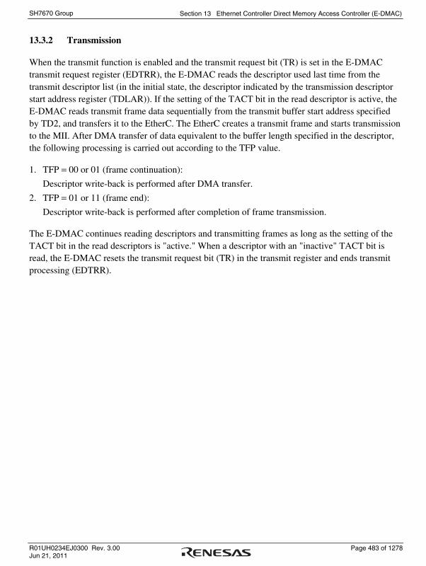
Section 13 Ethernet Controller Direct Memory Access Controller (E-DMAC)
R01UH0234EJ0300 Rev. 3.00 Page 483 of 1278 Jun 21, 2011
SH7670 Group
13.3.2 Transmission
When the transmit function is enabled and the transmit request bit (TR) is set in the E-DMAC transmit request register (EDTRR), the E-DMAC reads the descriptor used last time from the transmit descriptor list (in the initial state, the descriptor indicated by the transmission descriptor start address register (TDLAR)). If the setting of the TACT bit in the read descriptor is active, the E-DMAC reads transmit frame data sequentially from the transmit buffer start address specified by TD2, and transfers it to the EtherC. The EtherC creates a transmit frame and starts transmission to the MII. After DMA transfer of data equivalent to the buffer length specified in the descriptor, the following processing is carried out according to the TFP value.
1. TFP = 00 or 01 (frame continuation):
Descriptor write-back is performed after DMA transfer.
2. TFP = 01 or 11 (frame end):
Descriptor write-back is performed after completion of frame transmission. The E-DMAC continues reading descriptors and transmitting frames as long as the setting of the TACT bit in the read descriptors is "active." When a descriptor with an "inactive" TACT bit is read, the E-DMAC resets the transmit request bit (TR) in the transmit register and ends transmit processing (EDTRR).

Section 13 Ethernet Controller Direct Memory Access Controller (E-DMAC)
Page 484 of 1278 R01UH0234EJ0300 Rev. 3.00 Jun 21, 2011
SH7670 Group
This LSI + memory
Transmission flowchart
E-DMAC EtherC EthernetTransmit FIFO
EtherC/E-DMACinitialization
Descriptor andtransmit
buffer setting
Transmit directive
Descriptor read
Descriptor write-back
Descriptor write-back
Transmissioncompleted
Descriptor read
Transmit data transfer
Frame transmission
Transmit data transfer
Figure 13.4 Sample Transmission Flowchart

Section 13 Ethernet Controller Direct Memory Access Controller (E-DMAC)
R01UH0234EJ0300 Rev. 3.00 Page 485 of 1278 Jun 21, 2011
SH7670 Group
13.3.3 Reception
When the receive function is enabled and the CPU sets the receive request bit (RR) in the E-DMAC receive request register (EDRRR), the E-DMAC reads the descriptor following the previously used one from the receive descriptor list (the descriptor indicated by the receive descriptor list's starting address register (RDLA) is used at the initial state), and then enters the receive-standby state. If the setting of the RACT bit is "active" and an own-address frame is received, the E-DMAC transfers the frame to the receive buffer specified by RD2. If the data length of the received frame is greater than the buffer length given by RD1, the E-DMAC performs write-back to the descriptor when the buffer is full (RFP = 10 or 00), then reads the next descriptor. The E-DMAC then continues to transfer data to the receive buffer specified by the new RD2. When frame reception is completed, or if frame reception is suspended because of a certain kind of error, the E-DMAC performs write-back to the relevant descriptor (RFP = 11 or 01), and then ends the receive processing. The E-DMAC then reads the next descriptor and enters the receive-standby state again.
To receive frames continuously, the receive enable control bit (RNC) must be set to 1 in the receive control register (RCR). After initialization, this bit is cleared to 0.

Section 13 Ethernet Controller Direct Memory Access Controller (E-DMAC)
Page 486 of 1278 R01UH0234EJ0300 Rev. 3.00 Jun 21, 2011
SH7670 Group
This LSI + memory
Reception flowchart
E-DMAC EtherCReceive FIFO Ethernet
EtherC/E-DMACinitialization
Descriptor andreceive
buffer setting
Receptioncompleted
Receive data transfer
Receive data transfer
Frame reception
Start of reception
Descriptor read
Descriptor write-back
Descriptor write-back
Descriptor read (receiveready for the next frame)
Descriptor read
Figure 13.5 Sample Reception Flowchart

Section 13 Ethernet Controller Direct Memory Access Controller (E-DMAC)
R01UH0234EJ0300 Rev. 3.00 Page 487 of 1278 Jun 21, 2011
SH7670 Group
13.3.4 Multi-Buffer Frame Transmit/Receive Processing
Multi-Buffer Frame Transmit Processing
If an error occurs during multi-buffer frame transmission, the processing shown in figure 13.6 is carried out by the E-DMAC.
Where the transmit descriptor is shown as inactive (TACT bit = 0) in the figure, buffer data has already been transmitted normally, and where the transmit descriptor is shown as active (TACT bit = 1), buffer data has not been transmitted. If a frame transmit error occurs in the first descriptor part where the transmit descriptor is active (TACT bit = 1), transmission is halted, and the TACT bit cleared to 0, immediately. The next descriptor is then read, and the position within the transmit frame is determined on the basis of bits TFP1 and TFP0 (continuing [B'00] or end [B'01]). In the case of a continuing descriptor, the TACT bit is cleared to 0, only, and the next descriptor is read immediately. If the descriptor is the final descriptor, not only is the TACT bit cleared to 0, but write-back is also performed to the TFE and TFS bits at the same time. Data in the buffer is not transmitted between the occurrence of an error and write-back to the final descriptor. If error interrupts are enabled in the EtherC/E-DMAC status interrupt permission register (EESIPR), an interrupt is generated immediately after the final descriptor write-back.
0
0
0
1
1
1
1
1
1
0
0
0
0
0
0
0
0
1
1
0
0
0
0
0
0
0
1
0
0
0
0
0
0
0
1
0
E-DMACInactivates TACT (change 1 to 0)
Descriptor readInactivates TACT
Descriptor readInactivates TACT
Descriptor readInactivates TACT
Descriptor read
Inactivates TACT and writes TFE, TFS
Descriptors
Untransmitteddata is nottransmittedafter erroroccurrenceDescriptor isonly processed.
One frame
Buffer
Transmitted data
Untransmitted data
Transmit error occurrence
TACT
TDLE
TFP1
TFP0
Figure 13.6 E-DMAC Operation after Transmit Error
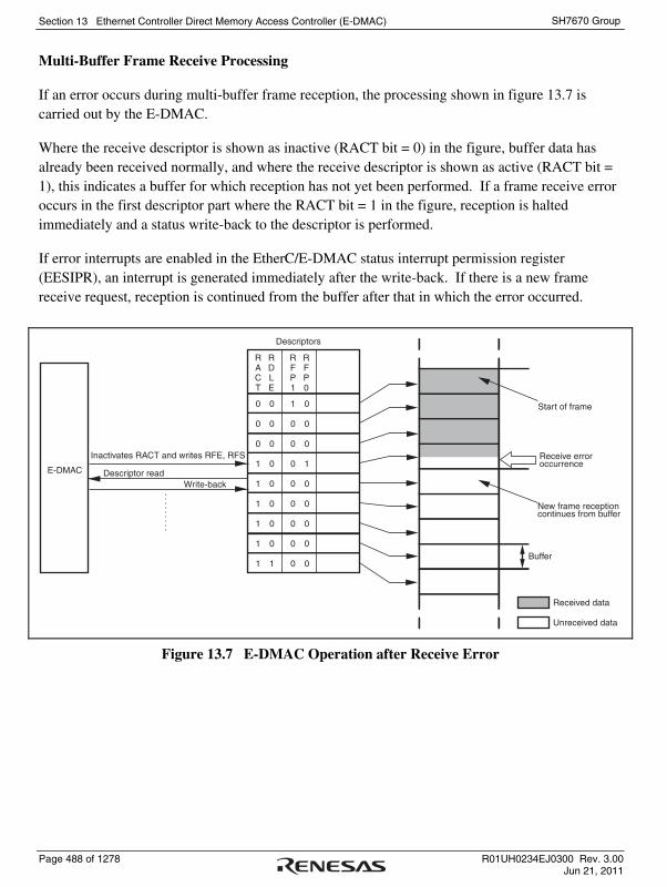
Section 13 Ethernet Controller Direct Memory Access Controller (E-DMAC)
Page 488 of 1278 R01UH0234EJ0300 Rev. 3.00 Jun 21, 2011
SH7670 Group
Multi-Buffer Frame Receive Processing
If an error occurs during multi-buffer frame reception, the processing shown in figure 13.7 is carried out by the E-DMAC.
Where the receive descriptor is shown as inactive (RACT bit = 0) in the figure, buffer data has already been received normally, and where the receive descriptor is shown as active (RACT bit = 1), this indicates a buffer for which reception has not yet been performed. If a frame receive error occurs in the first descriptor part where the RACT bit = 1 in the figure, reception is halted immediately and a status write-back to the descriptor is performed.
If error interrupts are enabled in the EtherC/E-DMAC status interrupt permission register (EESIPR), an interrupt is generated immediately after the write-back. If there is a new frame receive request, reception is continued from the buffer after that in which the error occurred.
E-DMAC
Inactivates RACT and writes RFE, RFS
Descriptor readWrite-back
Descriptors
Buffer
Received data
Unreceived data
Receive erroroccurrence
. . . . . . . . .
Start of frame
New frame receptioncontinues from buffer
0
0
0
1
1
1
1
1
1
0
0
0
0
0
0
0
0
1
1
0
0
0
0
0
0
0
0
0
0
0
1
0
0
0
0
0
RACT
RDLE
RFP1
RFP0
Figure 13.7 E-DMAC Operation after Receive Error

Section 13 Ethernet Controller Direct Memory Access Controller (E-DMAC)
R01UH0234EJ0300 Rev. 3.00 Page 489 of 1278 Jun 21, 2011
SH7670 Group
13.3.5 Padding Receive Data
The E-DMAC can pad one to three bytes anywhere in the receive data to increase the efficiency of processing of receive data. For example, by padding two bytes after the 14-byte MAC header of an Ethernet frame with this function, the subsequent data can be placed at the beginning of the four-byte boundary.
[No padding]
Receive buffer area16-byte boundary
Padding for separation in the 16-byte boundary
4 bytes
MAC header (14 bytes)
MAC header (14 bytes)
MAC header (14 bytes)
16-byte boundary
16-byte boundary
Padding for separation in the 16-byte boundary
[Padding]
Receive buffer area
Padding of two bytes after the 14th byte
16-byte boundary
Padding two bytes after the MAC header
4 bytes
MAC header (14 bytes)
MAC header (14 bytes)
MAC header (14 bytes)
16-byte boundary
16-byte boundary
Figure 13.8 Padding Receive Data

Section 13 Ethernet Controller Direct Memory Access Controller (E-DMAC)
Page 490 of 1278 R01UH0234EJ0300 Rev. 3.00 Jun 21, 2011
SH7670 Group
13.3.6 Checksum Calculation Function
Checksum calculation for receive packets is accelerated in the following two modes:
• Checksum calculation mode of MAC/IP packet analysis type
• All-data checksum calculation mode of skipped bytes designation type (1) Checksum Calculation Mode of MAC/IP Packet Analysis Type (CSEBL = 1 and CSMD
= 1)
Any receive packet included in the table below will be the target of calculation. Note that even when a receive packet is included in the table, checksum calculation is not done if the MAC packet payload contains padding data that has been inserted because the IP packet is small.
IPver Item
No option
Option provided
IPv4
Fragment*1
No extension header
Length of the extension header of a hop-by-hop option
Length of the extension header of routing
Length of the extension header of a fragment*1
Length of the extension header of an end-point option
Length of the extension header of AH
Length of the extension header of ESP*2
IPv6
Length of the extension header of MobileIPv6*2
Notes: *1. This is the target of calculation, but both RCS15 to RCS0 and RCSE will be undefined even if the data is normal.
*2. No calculation is performed on RCS15 to RCS0, and RCSE is set to 1.

Section 13 Ethernet Controller Direct Memory Access Controller (E-DMAC)
R01UH0234EJ0300 Rev. 3.00 Page 491 of 1278 Jun 21, 2011
SH7670 Group
The following shows the areas as the target of calculation of an IPv4 packet. The shaded portions are the target of calculation.
0
Packet length
IPv4/IPv6/others (Decision) IHL*
An option, if any, is deleted from the target of calculation.
Data
Receive IP address
Transmit IP address Receive IP address
Transmit IP address
No. 31 16 15 11 8 7 0
1
2
3
4
5
6
7
8
9
10
Note: * This is changed to the octet basis and undergoes a subtraction during checksum calculation. During calculation, {8'h00, protocol No.[7:0]} is used.

Section 13 Ethernet Controller Direct Memory Access Controller (E-DMAC)
Page 492 of 1278 R01UH0234EJ0300 Rev. 3.00 Jun 21, 2011
SH7670 Group
The following shows the areas as the target of calculation of an IPv6 packet. The shaded portions are the target of calculation.
0
Next header*1
Next header*1 Header length*2
IPv4/IPv6/others (Decision)
Payload length
The content of an extension header is not the target of checksum calculation.
Data
Receive IP addressTransmit IP address
Receive IP address
Transmit IP address
Transmit IP address
Transmit IP address
Receive IP address
Receive IP address
Receive IP address
Transmit IP address
No. 31 16 15 0
1
2
3
4
5
6
7
8
9
10
11
12
13
Note: 1. Calculation applies only to TCP/UDP. Calculation requires an expansion to {8'h00, next header[7:0]}. 2. This is changed to the octet basis and undergoes a subtraction during checksum calculation.

Section 13 Ethernet Controller Direct Memory Access Controller (E-DMAC)
R01UH0234EJ0300 Rev. 3.00 Page 493 of 1278 Jun 21, 2011
SH7670 Group
(2) All-Data Checksum Calculation Mode of Skipped Bytes Designation Type (CSEBL = 1 and CSMD = 0)
The data equivalent to the number of bytes specified by SB5 to SB0 is skipped from the beginning of a packet, and checksums are calculated on all of the subsequent valid data. (Example: 14-byte skip)
0
Data to be calculated
SB[5:0]OE
No. 31 16 15 0
1
2
3
4
5
6
7
8
9
10
11
13.3.7 Usage Notes
The checksum calculation function is not affected by the padding function specified through the receive data padding setting register (RPADIR). Checksums are calculated when the receive data is transferred from the EtherC to the E-DMAC, whereas the receive data is padded when it is transferred from the E-DMAC to the receive buffer in memory.

Section 13 Ethernet Controller Direct Memory Access Controller (E-DMAC)
Page 494 of 1278 R01UH0234EJ0300 Rev. 3.00 Jun 21, 2011
SH7670 Group
Section 14 DMAC That Works with Encryption/Decryption and Forward Error Correction Core (A-DMAC)
R01UH0234EJ0300 Rev. 3.00 Page 495 of 1278 Jun 21, 2011
SH7670 Group
Section 14 DMAC That Works with Encryption/Decryption and Forward Error Correction Core (A-DMAC)
14.1 Overview
The A-DMAC is a high-level descriptor-mode DMAC having error correction function. This DMAC provides data transfer with memory via an internal shared bus (I-BUS) and data transfer with an external MPEG device via STIF.
14.1.1 Features
The functions and features of this A-DMAC are as follows:
(1) Channels for checksum processing
• Number of channels: 2
• Transfer direction: Memory← →memory, memory← →STIF
• Descriptor structure: Structure that enables checksum operation, etc., to be continuously performed
• Error check: Checksum calculation function
(2) FEC channels
• Number of channels: 1
• Descriptor structure: Structure that enables processing of any number of data items with a small number of buffers
• Error correction (FEC): XOR calculation function (3) Other features
• Supported endian: Big endian/little endian
• Number of STIFs connected: Two channels
• Channel arbitration: Round robin scheduling that provides highly efficient use of encryption modules and buses
• Channel operation: Parallel processing

Section 14 DMAC That Works with Encryption/Decryption and Forward Error Correction Core (A-DMAC)
Page 496 of 1278 R01UH0234EJ0300 Rev. 3.00 Jun 21, 2011
SH7670 Group
14.1.2 Overall Configuration of the A-DMAC
The A-DMAC is configured as shown in figure 14.1. Table 14.1 gives an overview of A-DMAC submodules.
The A-DMAC is connected to the I-BUS via the I-BUS interface, to the STIF0 via the STIF0 interface, and to the STIF1 via the STIF1 interface. The I-BUS is a shared bus in this LSI operating on the B clock. The STIF is an I/O port for MPEG-2 TS/PS format data. The STIF0 is fixed at CH0 and the STIF1 fixed at CH1.
The A-DMAC has two channels for checksum operation that operate on descriptors. Aside from these channels, the A-DMAC has an FEC channel dedicated for FEC operation. This FEC channel performs XOR operation of FEC operation.
These modules operate in parallel. For example, when the bus for channel 0 for checksum processing is accessed, channel 1 for checksum processing can perform checksum operation.
The arbiter is a module that arbitrates the requests sent from each checksum processing channel and each initiator of the FEC channel. The arbiter arbitrates requests from an initiator in round robin scheduling. If you want to execute CH0 and CH1 simultaneously and raise the priority of CH0 or CH1, the arbiter controls the priorities in descriptor ring units (example: When the descriptor of CH0 or CH1, whichever has a lower priority, runs dry, the arbiter piles up the next descriptor after a certain idling) or controls the priorities by suspending channel processing of lower priority.

Section 14 DMAC That Works with Encryption/Decryption and Forward Error Correction Core (A-DMAC)
R01UH0234EJ0300 Rev. 3.00 Page 497 of 1278 Jun 21, 2011
SH7670 Group
A-DMAC
CPU control
Channel0 control BUS I/F control
BUS I/F data
I-BUS control
INTC
STIF0
STIF1
Arbiter
Function· Arbitration
I-BUS
Channel 0 for checksum
Function
Function
· DMA automatic processing· Checksum operation· Processing data management, Data selector
Channel 1 for checksum
· DMA automatic processing· Checksum operation· Processing data management, Data selector
Function
I-BUSinterface
· Bus protocol conversion
STIF0interface
· STIF0 protocol conversion
STIF1interface
· STIF1 protocol conversion
Function
Function
Function
FEC channel
· DMA autmatic processing· XOR operation
I-BUS data
STIF0control
STIF0 data
STIF1 control
STIF1 data
STIF0 I/F control
STIF0 I/F data
STIF1 I/F control
STIF1 I/F data
Channel0 data
Channel1 control
Channel1 data
FEC channel control
FEC channel data
CPU control data
ADMA interrupt
ad_irqc0_n
ad_irqc1_n
ad_irqfec_n
x_rst
x_bck
x_bckstp_p
x_modstp_p
Figure 14.1 Block Diagram of A-DMAC

Section 14 DMAC That Works with Encryption/Decryption and Forward Error Correction Core (A-DMAC)
Page 498 of 1278 R01UH0234EJ0300 Rev. 3.00 Jun 21, 2011
SH7670 Group
Table 14.1 A-DMAC Submodules
Submodule Name Function
Channel for checksum processing
• DMA automatic processing based on descriptors
• Checksum operation
• Continuous execution of checksum
FEC channel • DMA automatic processing based on descriptors
• XOR operation for any number of data items
Arbiter • Arbitrates requests from the channel for checksum processing
and FEC channel.
• Channel arbitration mode is round robin scheduling.
I-BUS interface • Conversion between I-BUS protocol and A-DMAC protocol
• Distribution of register R/W requests from the CPU to each
module
STIF interface • Conversion between STIF protocol and A-DMAC protocol
• STIF0 is fixed at channel 0 for encryption/authentication.
• STIF1 is fixed at channel 1 for encryption/authentication.
Section 14 DMAC That Works with Encryption/Decryption and Forward Error Correction Core (A-DMAC)
R01UH0234EJ0300 Rev. 3.00 Page 499 of 1278 Jun 21, 2011
SH7670 Group
14.1.3 Restrictions on the A-DMAC
The following restrictions apply to the A-DMAC:
• The A-DMAC supports only register access in 32-bit units.
• If the channel processor, or FEC processor is running, write to registers related to the appropriate processor is inhibited. However, you can write data to the following two registers by verifying them after the write even if the appropriate processor is running. Write data repeatedly till verify succeeds.
⎯ Channel [i] processing control register (C[i]C) (However, do not rewrite the C[i]C_R bit of the running channel processor.)
⎯ Channel [i] processing interrupt request register (C[i]I)
• Descriptors of data size 0 are inhibited.

Section 14 DMAC That Works with Encryption/Decryption and Forward Error Correction Core (A-DMAC)
Page 500 of 1278 R01UH0234EJ0300 Rev. 3.00 Jun 21, 2011
SH7670 Group
14.2 Register Descriptions
The A-DMAC has the following registers. For details on the addresses of these registers and the register status in each processing state, see section 28, List of Registers.
• Channel [i] processing control register (C[i]C) (i = 0, 1)
• Channel [i] processing mode register (C[i]M) (i = 0, 1)
• Channel [i] processing interrupt request register (C[i]I) (i = 0, 1)
• Channel [i] processing descriptor start address register (C[i]DSA) (i = 0, 1)
• Channel [i] processing descriptor current address register (C[i]DCA) (i = 0, 1)
• Channel [i] processing descriptor 0 register (C[i]D0) [control] (i = 0, 1)
• Channel [i] processing descriptor 1 register (C[i]D1) [source address] (i = 0, 1)
• Channel [i] processing descriptor 2 register (C[i]D2) [destination address] (i = 0, 1)
• Channel [i] processing descriptor 3 register (C[i]D3) [data length] (i = 0, 1)
• Channel [i] processing descriptor 4 register (C[i]D4) [checksum value write address] (i = 0, 1)
• FEC DMAC processing control register (FECC)
• FEC DMAC processing interrupt request register (FECI)
• FEC DMAC processing descriptor start address register (FECDSA)
• FEC DMAC processing descriptor current address register (FECDCA)
• FEC DMAC processing descriptor 0 register (FECD00) [control]
• FEC DMAC processing descriptor 1 register (FECD01D0A) [destination address]
• FEC DMAC processing descriptor 2 register (FECD02S0A) [source 0 address]
• FEC DMAC processing descriptor 3 register (FECD03S1A) [source 1 address]
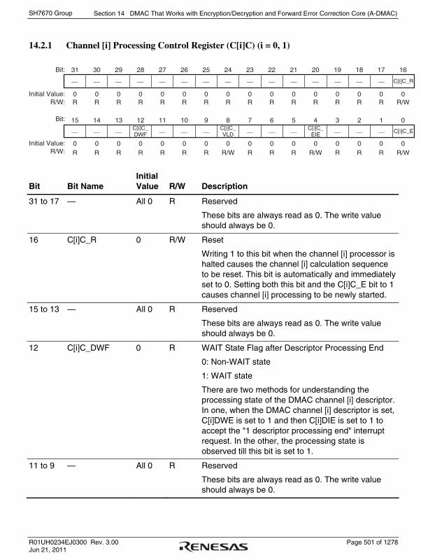
Section 14 DMAC That Works with Encryption/Decryption and Forward Error Correction Core (A-DMAC)
R01UH0234EJ0300 Rev. 3.00 Page 501 of 1278 Jun 21, 2011
SH7670 Group
14.2.1 Channel [i] Processing Control Register (C[i]C) (i = 0, 1)
31 30 29 28 27 26 25 24 23 22 21 20 19 18 17 16Bit:
Initial Value:R/W:
Bit:
Initial Value:R/W:
15 14 13 12 11 10 9 8 7 6 5 4 3 2 1 0
0 0 0 0 0 0 0 0 0 0 0 0 0 0 0 0R R R R R R R R R R R R R R R R/W
0 0 0 0 0 0 0 0 0 0 0 0 0 0 0 0R R R R R R R R/W R R R R/W R R R R/W
⎯ ⎯ ⎯ ⎯ ⎯ ⎯ ⎯ ⎯ ⎯ ⎯ ⎯ ⎯ ⎯ ⎯ ⎯
⎯ ⎯ ⎯C[i]C_DWF ⎯ ⎯ ⎯
C[i]C_VLD ⎯ ⎯ ⎯
C[i]C_EIE ⎯ ⎯ ⎯
C[i]C_R
C[i]C_E
Bit Bit Name Initial Value R/W Description
31 to 17 — All 0 R Reserved
These bits are always read as 0. The write value should always be 0.
16 C[i]C_R 0 R/W Reset
Writing 1 to this bit when the channel [i] processor is halted causes the channel [i] calculation sequence to be reset. This bit is automatically and immediately set to 0. Setting both this bit and the C[i]C_E bit to 1 causes channel [i] processing to be newly started.
15 to 13 — All 0 R Reserved
These bits are always read as 0. The write value should always be 0.
12 C[i]C_DWF 0 R WAIT State Flag after Descriptor Processing End
0: Non-WAIT state
1: WAIT state
There are two methods for understanding the processing state of the DMAC channel [i] descriptor. In one, when the DMAC channel [i] descriptor is set, C[i]DWE is set to 1 and then C[i]DIE is set to 1 to accept the "1 descriptor processing end" interrupt request. In the other, the processing state is observed till this bit is set to 1.
11 to 9 — All 0 R Reserved
These bits are always read as 0. The write value should always be 0.

Section 14 DMAC That Works with Encryption/Decryption and Forward Error Correction Core (A-DMAC)
Page 502 of 1278 R01UH0234EJ0300 Rev. 3.00 Jun 21, 2011
SH7670 Group
Bit Bit Name Initial Value R/W Description
8 C[i]C_VLD 0 R/W Variable-Length Descriptor Control Flag
0: Fixed-length descriptor (32 bytes)
1: Variable-length descriptor (16/32 bytes)
The A-DMAC channel uses the 32-byte fixed length structure or 16/32-byte variable-length structure. If this bit is set to 0 to define the descriptor as the fixed-length, the descriptor is always read as 32 bytes. If this bit is set to 1 to define the descriptor as the variable-length, the first 16 bytes are read, and if r_cid4/r_cid5/r_cid6/r_cid7 information is required, the remaining 16 bytes are read according to the contents of r_cidm/r_cihm.
7 to 5 — All 0 R Reserved
These bits are always read as 0. The write value should always be 0.
4 C[i]C_EIE 0 R/W "Processing End" Interrupt Request Enable
When processing ends, specifies whether to enable or disable the "processing end" interrupt request.
0: Disables the "processing end" interrupt request.
1: Enables the "processing end" interrupt request.
A-DMAC channel [i] processing end means fetching of depleted descriptors (invalid descriptors (descriptors where C[i]F0 is set to 0)).
3 to 1 — All 0 R Reserved
These bits are always read as 0. The write value should always be 0.

Section 14 DMAC That Works with Encryption/Decryption and Forward Error Correction Core (A-DMAC)
R01UH0234EJ0300 Rev. 3.00 Page 503 of 1278 Jun 21, 2011
SH7670 Group
Bit Bit Name Initial Value R/W Description
0 C[i]C_E 0 R/W Execution Request
Setting this bit to 1 causes channel [i] processing to be started. Setting this bit to 0 causes channel [i] processing to be suspended. When 0 is written to this bit, 0 is read immediately but the channel [i] processor does not stop immediately. That is, the processor stops after it writes back to the descriptor being processed. To understand the channel operating state, set the C[i]C_EIE bit to 1 to accept the "operation end" interrupt request or poll the "operation end" interrupt request flag. To start new processing, the channel [i] of the STIF must be initialized.
0: Channel [i] processing is halted.
1: Channel [i] processing is in progress.
Determine if channel [i] processing is suspended when the processor writes back to the descriptor.

Section 14 DMAC That Works with Encryption/Decryption and Forward Error Correction Core (A-DMAC)
Page 504 of 1278 R01UH0234EJ0300 Rev. 3.00 Jun 21, 2011
SH7670 Group
14.2.2 Channel [i] Processing Mode Register (C[i]M) (i = 0, 1)
31 30 29 28 27 26 25 24 23 22 21 20 19 18 17 16Bit:
Initial Value:R/W:
Bit:
Initial Value:R/W:
15 14 13 12 11 10 9 8 7 6 5 4 3 2 1 0
0 0 0 0 0 0 0 0 0 0 0 0 0 0 0 0R R R R R R R R R R R R R R R R
0 0 0 0 0 0 0 0 0 0 0 0 0 0 0 0R R R R R R R R R R R R/W R R R R
⎯ ⎯ ⎯ ⎯ ⎯ ⎯ ⎯ ⎯ ⎯ ⎯ ⎯ ⎯ ⎯ ⎯ ⎯
⎯ ⎯ ⎯ ⎯ ⎯ ⎯ ⎯ ⎯ ⎯ ⎯ ⎯C[i]M_
LIE ⎯ ⎯ ⎯
⎯
⎯
Bit Bit Name Initial Value R/W Description
31 to 5 — All 0 R Reserved
These bits are always read as 0. The write value should always be 0.
4 C[i]M_LIE 0 R/W "Last Data Descriptor End Processing" Interrupt Request Enable
When last data (C[i]F2=1) descriptor end processing ends, specifies whether to enable or disable the interrupt request.
0: Disables the "last data descriptor processing
end" interrupt request.
1: Enables the "last data descriptor processing end"
interrupt request.
3 to 0 — All 0 R Reserved
These bits are always read as 0. The write value should always be 0.

Section 14 DMAC That Works with Encryption/Decryption and Forward Error Correction Core (A-DMAC)
R01UH0234EJ0300 Rev. 3.00 Page 505 of 1278 Jun 21, 2011
SH7670 Group
14.2.3 Channel [i] Processing Interrupt Request Register (C[i]I) (i = 0, 1)
ad_irqc[i]_n is asserted as negation of logical OR of all bits in this register.
31 30 29 28 27 26 25 24 23 22 21 20 19 18 17 16Bit:
Initial Value:R/W:
Bit:
Initial Value:R/W:
15 14 13 12 11 10 9 8 7 6 5 4 3 2 1 0
0 0 0 0 0 0 0 0 0 0 0 0 0 0 0 0R R R R R R R R R R R R R R R R
0 0 0 0 0 0 0 0 0 0 0 0 0 0 0 0R R R R/W R R R R/W R R R R R R R R/W
⎯ ⎯ ⎯ ⎯ ⎯ ⎯ ⎯ ⎯ ⎯ ⎯ ⎯ ⎯ ⎯ ⎯ ⎯
⎯ ⎯ ⎯C[i]I_
DI ⎯ ⎯ ⎯C[i]I_
LI ⎯ ⎯ ⎯ ⎯ ⎯ ⎯ ⎯
⎯
C[i]I_EI
Bit Bit Name Initial Value R/W Description
31 to 13 — All 0 R Reserved
These bits are always read as 0. The write value should always be 0.
12 C[i]I_DI 0 R/W "1 Descriptor Processing End" Interrupt Request (interrupt request to notify you that the processor ended descriptor processing and wrote back the descriptor)
This bit is cleared to 0 by writing 1 to it. When 0 is written to this bit, the current state is retained.
0: The "1 descriptor processing end" interrupt is not
requested.
1: The "1 descriptor processing end" interrupt is
requested.
11 to 9 — All 0 R Reserved
These bits are always read as 0. The write value should always be 0.
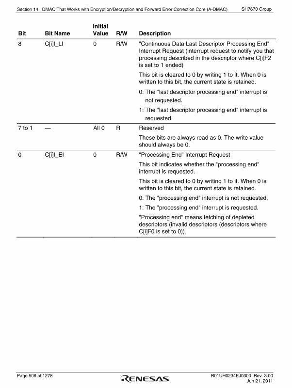
Section 14 DMAC That Works with Encryption/Decryption and Forward Error Correction Core (A-DMAC)
Page 506 of 1278 R01UH0234EJ0300 Rev. 3.00 Jun 21, 2011
SH7670 Group
Bit Bit Name Initial Value R/W Description
8 C[i]I_LI 0 R/W "Continuous Data Last Descriptor Processing End" Interrupt Request (interrupt request to notify you that processing described in the descriptor where C[i]F2 is set to 1 ended)
This bit is cleared to 0 by writing 1 to it. When 0 is written to this bit, the current state is retained.
0: The "last descriptor processing end" interrupt is
not requested.
1: The "last descriptor processing end" interrupt is
requested.
7 to 1 — All 0 R Reserved
These bits are always read as 0. The write value should always be 0.
0 C[i]I_EI 0 R/W "Processing End" Interrupt Request
This bit indicates whether the "processing end" interrupt is requested.
This bit is cleared to 0 by writing 1 to it. When 0 is written to this bit, the current state is retained.
0: The "processing end" interrupt is not requested.
1: The "processing end" interrupt is requested.
"Processing end" means fetching of depleted descriptors (invalid descriptors (descriptors where C[i]F0 is set to 0)).

Section 14 DMAC That Works with Encryption/Decryption and Forward Error Correction Core (A-DMAC)
R01UH0234EJ0300 Rev. 3.00 Page 507 of 1278 Jun 21, 2011
SH7670 Group
14.2.4 Channel [i] Processing Descriptor Start Address Register (C[i]DSA) (i = 0, 1)
Do not write any value to this register when C[i]C_E is set to 1.
31 30 29 28 27 26 25 24 23 22 21 20 19 18 17 16Bit:
Initial Value:R/W:
Bit:
Initial Value:R/W:
15 14 13 12 11 10 9 8 7 6 5 4 3 2 1 0
0 0 0 0 0 0 0 0 0 0 0 0 0 0 0 0R/W R/W R/W R/W R/W R/W R/W R/W R/W R/W R/W R/W R/W R/W R/W R/W
0 0 0 0 0 0 0 0 0 0 0 0 0 0 0 0R/W R/W R/W R/W R/W R/W R/W R/W R/W R/W R/W R/W R R R R
C[i]DSA[3:0]
C[i]DSA[31:16]
C[i]DSA[15:4]
Bit Bit Name Initial Value R/W Description
31 to 4 C[i]DSA[31:4] All 0 R/W
3 to 0 C[i]DSA[3:0] All 0 R
Descriptor Ring Start Address
Specify a descriptor ring start address. Set a 16-byte boundary address value.
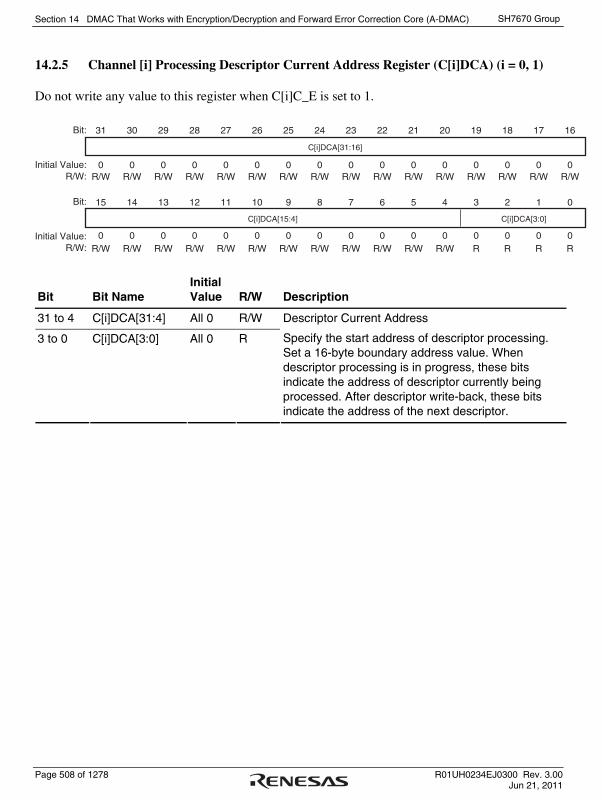
Section 14 DMAC That Works with Encryption/Decryption and Forward Error Correction Core (A-DMAC)
Page 508 of 1278 R01UH0234EJ0300 Rev. 3.00 Jun 21, 2011
SH7670 Group
14.2.5 Channel [i] Processing Descriptor Current Address Register (C[i]DCA) (i = 0, 1)
Do not write any value to this register when C[i]C_E is set to 1.
31 30 29 28 27 26 25 24 23 22 21 20 19 18 17 16Bit:
Initial Value:R/W:
Bit:
Initial Value:R/W:
15 14 13 12 11 10 9 8 7 6 5 4 3 2 1 0
0 0 0 0 0 0 0 0 0 0 0 0 0 0 0 0R/W R/W R/W R/W R/W R/W R/W R/W R/W R/W R/W R/W R/W R/W R/W R/W
0 0 0 0 0 0 0 0 0 0 0 0 0 0 0 0R/W R/W R/W R/W R/W R/W R/W R/W R/W R/W R/W R/W R R R R
C[i]DCA[3:0]
C[i]DCA[31:16]
C[i]DCA[15:4]
Bit Bit Name Initial Value R/W Description
31 to 4 C[i]DCA[31:4] All 0 R/W
3 to 0 C[i]DCA[3:0] All 0 R
Descriptor Current Address
Specify the start address of descriptor processing. Set a 16-byte boundary address value. When descriptor processing is in progress, these bits indicate the address of descriptor currently being processed. After descriptor write-back, these bits indicate the address of the next descriptor.

Section 14 DMAC That Works with Encryption/Decryption and Forward Error Correction Core (A-DMAC)
R01UH0234EJ0300 Rev. 3.00 Page 509 of 1278 Jun 21, 2011
SH7670 Group
14.2.6 Channel [i] Processing Descriptor 0 Register (C[i]D0) [Control] (i = 0, 1)
Do not write any value to this register when C[i]C_E is set to 1.
31 30 29 28 27 26 25 24 23 22 21 20 19 18 17 16Bit:
Initial Value:R/W:
Bit:
Initial Value:R/W:
15 14 13 12 11 10 9 8 7 6 5 4 3 2 1 0
0 0 0 0 0 0 0 0 0 0 0 0 0 0 0 0R/W R/W R/W R/W R/W R/W R/W R/W R/W R/W R/W R/W R/W R/W R/W R/W
0 0 0 0 0 0 0 0 0 0 0 0 0 0 0 0R/W R/W R/W R/W R/W R/W R/W R/W R/W R/W R/W R/W R/W R/W R/W R/W
C[i]CRDO[3:0] C[i]CHDO[3:0] C[i]SO[3:0] C[i]DA C[i]SA C[i]CSM[1:0]
⎯ ⎯ ⎯ ⎯ ⎯ ⎯ ⎯ ⎯ ⎯ ⎯ ⎯ ⎯ ⎯ C[i]F2 C[i]F1 C[i]F0
Bit Bit Name Initial Value R/W Description
31 to 28 C[i]CRDO[3:0] All 0 R/W Transfer Data Destination Data Sequence
Specify a swap method for writing transfer data after encryption processing from the A-DMAC to memory such as the STIF and SDRAM or after checksum operation. Specify a swap method for writing the checksum operation result obtained from body data in the C[i]CHDO3 to C[i]CHDO0 bits, not these bits.

Section 14 DMAC That Works with Encryption/Decryption and Forward Error Correction Core (A-DMAC)
Page 510 of 1278 R01UH0234EJ0300 Rev. 3.00 Jun 21, 2011
SH7670 Group
Bit Bit Name Initial Value R/W Description
31 to 28 C[i]CRDO[3:0] All 0 R/W • When the destination is not the STIF (C[i]DA bit
= 0)
C[i]CRDO3: Data swap in two-byte units (longword swap in word units)
0: As-is 1: Swap
C[i]CRDO2: Data swap in one-byte units (word swap in byte units)
0: As-is 1: Swap
C[i]CRDO1: Inversion of bit 1 at address when one or two bytes are accessed
0: As-is 1: Inversion
C[i]CRDO0: Inversion of bit 0 at address when one byte is accessed
0: As-is 1: Inversion
C[i]CRDO1 and C[i]CRDO0 function for endian adjustment. Note that if an endian different from the endian of this LSI is used, up to three different addresses are accessed from the address where the start and end addresses are specified when an area is allocated.
• When the destination is the STIF (C[i]DA bit = 1)
C[i]CRDO3: Data swap in two-byte units (longword swap in word units)
0: As-is 1: Swap
C[i]CRDO2: Data swap in one-byte units (word swap in byte units)
0: As-is 1: Swap
C[i]CRDO1: Data swap in one-bit units (byte swap in one-bit units)
0: As-is 1: Swap
C[i]CRDO0: Set this bit to 0 as reserved.

Section 14 DMAC That Works with Encryption/Decryption and Forward Error Correction Core (A-DMAC)
R01UH0234EJ0300 Rev. 3.00 Page 511 of 1278 Jun 21, 2011
SH7670 Group
Bit Bit Name Initial Value R/W Description
27 to 24 C[i]CHDO[3:0] All 0 R/W Checksum Operation Result Destination Data Sequence
Specify a swap method for writing the checksum operation result from the A-DMAC to memory such as SDRAM. Specify a swap method for writing body data after checksum operation in the C[i]CRDO3 to C[i]CRDO0 bits.
C[i]CHDO3: Data swap in two-byte units (longword swap in word units)
0: As-is
1: Swap
C[i]CHDO2: Data swap in one-byte units (word swap in byte units)
0: As-is
1: Swap
C[i]CHDO1: Inversion of bit 1 at address when one or two bytes are accessed
0: As-is 1: Inversion
C[i]CHDO0: Inversion of bit 0 at address when one byte is accessed
0: As-is 1: Inversion
C[i]CHDO1 and C[i]CHDO0 function for endian adjustment. Note that if an endian different from the endian of this LSI is used, up to three different addresses are accessed from the address where the start and end addresses are specified when an area is allocated.

Section 14 DMAC That Works with Encryption/Decryption and Forward Error Correction Core (A-DMAC)
Page 512 of 1278 R01UH0234EJ0300 Rev. 3.00 Jun 21, 2011
SH7670 Group
Bit Bit Name Initial Value R/W Description
23 to 20 C[i]SO[3:0] All 0 R/W Source Data Sequence
Specify a swap method for reading data from memory such as the STIF and SDRAM to the A-DMAC.
• When the source is not the STIF (C[i]SA bit = 0)
C[i]SO3: Data swap in two-byte units (longword swap in word units) 0: As-is 1: Swap C[i]SO2: Data swap in one-byte units (word swap in byte units)0: As-is 1: Swap C[i]SO1: Inversion of bit 1 at address when one or two bytes are accessed 0: As-is 1: Inversion C[i]SO0: Inversion of bit 0 at address when one byte is accessed 0: As-is 1: Inversion C[i]SO1 and C[i]SO0 function for endian adjustment. Note that if an endian different from the endian of this LSI is used, up to three different addresses are accessed from the address where the start and end addresses are specified when an area is allocated.
• When the source is the STIF (C[i]SA bit = 1)
C[i]SO3: Data swap in two-byte units (longword swap in word units) 0: As-is 1: Swap C[i]SO2: Data swap in one-byte units (word swap in byte units)0: As-is 1: Swap C[i]SO1: Data swap in one-bit units (byte swap in one-bit units)0: As-is 1: Swap C[i]SO0: Set this bit to 0 as reserved. This bit is referenced in AES encryption/decryption, DES/3DES encryption/decryption, SHA hash generation, HMAC keyed hash generation, target data read for checksum operation, and data copy from memory to the STIF and from the STIF to memory. However, this bit is not referenced in key copy and initial vector copy.

Section 14 DMAC That Works with Encryption/Decryption and Forward Error Correction Core (A-DMAC)
R01UH0234EJ0300 Rev. 3.00 Page 513 of 1278 Jun 21, 2011
SH7670 Group
Bit Bit Name Initial Value R/W Description
19 C[i]DA 0 R/W Destination Attribute
Specifies whether the data read source uses the channel [i] (the destination address is not used) of the STIF or the destination address (memory such as SDRAM).
0: Uses the destination address (memory such as
SDRAM).
1: Uses the channel [i] of the STIF
18 C[i]SA 0 R/W Source Attribute
Specifies whether the data read source uses the channel [i] (the source address is not used) of the STIF or the source address (memory such as SDRAM).
0: Uses the source address (memory such as SDRAM).
1: Uses the channel [i] of the STIF
17, 16 C[i]CSM[1:0] 00 R/W Checksum Mode
00: Checksum (not initialized, not written back)
Not beginning of data
Not end of data
01: Checksum (not initialized, written back)
Not beginning of data
End of data
10: Checksum (initialized, not written back)
Beginning of data
Not end of data
11: Checksum (initialized, written back)
Beginning of data
End of data
15 to 3 — All 0 R/W Reserved
These bits are always read as 0. The write value should always be 0.

Section 14 DMAC That Works with Encryption/Decryption and Forward Error Correction Core (A-DMAC)
Page 514 of 1278 R01UH0234EJ0300 Rev. 3.00 Jun 21, 2011
SH7670 Group
Bit Bit Name Initial Value R/W Description
2 C[i]F2 0 R/W Descriptor Execution Flag 2
When splitting continuous data into several descriptors for execution, set this bit to 1 in the descriptor that processes the last data part (because the pointer in the A-DMAC must be initialized to process the next descriptor).
Use this flag when splitting and executing descriptors because the encryption/decryption part, authentication part, and checksum operation part in data such as IPsec/TLS differ.
0: Non-last descriptor that processes continuous data
1: Last descriptor that processes continuous data
1 C[i]F1 0 R/W Descriptor Execution Flag 1
When this bit is 1, the A-DMAC regards this descriptor as the last descriptor in the descriptor ring area. When processing of this descriptor ends, the A-DMAC returns to the beginning (descriptor start address) of the descriptor ring area.
0: Non-last descriptor ring
1: Last descriptor ring
0 C[i]F0 0 R/W Descriptor Execution Flag 0
When this bit is 0, the A-DMAC ends processing because this descriptor is invalid. When this bit is 1, this descriptor is valid. When this bit is 1 (valid descriptor), the A-DMAC sets this bit to 0 and writes back to the original address after processing of this descriptor ends.
0: Invalid descriptor
1: Valid descriptor

Section 14 DMAC That Works with Encryption/Decryption and Forward Error Correction Core (A-DMAC)
R01UH0234EJ0300 Rev. 3.00 Page 515 of 1278 Jun 21, 2011
SH7670 Group
14.2.7 Channel [i] Processing Descriptor 1 Register (C[i]D1) [Source Address] (i = 0, 1)
Do not write any value to this register when C[i]C_E is set to 1.
31 30 29 28 27 26 25 24 23 22 21 20 19 18 17 16Bit:
Initial Value:R/W:
Bit:
Initial Value:R/W:
15 14 13 12 11 10 9 8 7 6 5 4 3 2 1 0
0 0 0 0 0 0 0 0 0 0 0 0 0 0 0 0R/W R/W R/W R/W R/W R/W R/W R/W R/W R/W R/W R/W R/W R/W R/W R/W
0 0 0 0 0 0 0 0 0 0 0 0 0 0 0 0R/W R/W R/W R/W R/W R/W R/W R/W R/W R/W R/W R/W R/W R/W R/W R/W
C[i]D1[31:16]
C[i]D1[15:0]
Bit Bit Name Initial Value R/W Description
31 to 0 C[i]D1[31:0] All 0 R/W Source Address
Specify a source address. This register is used when source access involves memory reference. It is not used in the STIF.
When copying a key or initial vector from the source, set 0000 in the lower four bits (16-byte boundary).
When splitting continuous data into several descriptors for execution, specify the same source address in all the descriptors.
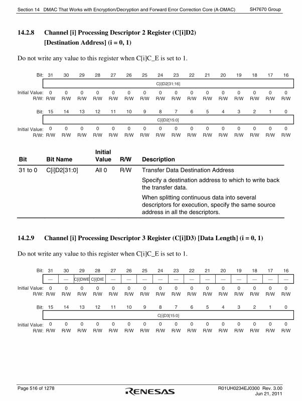
Section 14 DMAC That Works with Encryption/Decryption and Forward Error Correction Core (A-DMAC)
Page 516 of 1278 R01UH0234EJ0300 Rev. 3.00 Jun 21, 2011
SH7670 Group
14.2.8 Channel [i] Processing Descriptor 2 Register (C[i]D2)
[Destination Address] (i = 0, 1)
Do not write any value to this register when C[i]C_E is set to 1.
31 30 29 28 27 26 25 24 23 22 21 20 19 18 17 16Bit:
Initial Value:R/W:
Bit:
Initial Value:R/W:
15 14 13 12 11 10 9 8 7 6 5 4 3 2 1 0
0 0 0 0 0 0 0 0 0 0 0 0 0 0 0 0R/W R/W R/W R/W R/W R/W R/W R/W R/W R/W R/W R/W R/W R/W R/W R/W
0 0 0 0 0 0 0 0 0 0 0 0 0 0 0 0R/W R/W R/W R/W R/W R/W R/W R/W R/W R/W R/W R/W R/W R/W R/W R/W
C[i]D2[31:16]
C[i]D2[15:0]
Bit Bit Name Initial Value R/W Description
31 to 0 C[i]D2[31:0] All 0 R/W Transfer Data Destination Address
Specify a destination address to which to write back the transfer data.
When splitting continuous data into several descriptors for execution, specify the same source address in all the descriptors.
14.2.9 Channel [i] Processing Descriptor 3 Register (C[i]D3) [Data Length] (i = 0, 1)
Do not write any value to this register when C[i]C_E is set to 1.
31 30 29 28 27 26 25 24 23 22 21 20 19 18 17 16Bit:
Initial Value:R/W:
Bit:
Initial Value:R/W:
15 14 13 12 11 10 9 8 7 6 5 4 3 2 1 0
⎯ ⎯ C[i]DWE C[i]DIE ⎯ ⎯ ⎯ ⎯ ⎯ ⎯ ⎯ ⎯ ⎯ ⎯ ⎯ ⎯
C[i]D3[15:0]
0 0 0 0 0 0 0 0 0 0 0 0 0 0 0 0R/W R/W R/W R/W R/W R/W R/W R/W R/W R/W R/W R/W R/W R/W R/W R/W
0 0 0 0 0 0 0 0 0 0 0 0 0 0 0 0R/W R/W R/W R/W R/W R/W R/W R/W R/W R/W R/W R/W R/W R/W R/W R/W

Section 14 DMAC That Works with Encryption/Decryption and Forward Error Correction Core (A-DMAC)
R01UH0234EJ0300 Rev. 3.00 Page 517 of 1278 Jun 21, 2011
SH7670 Group
Bit Bit Name Initial Value R/W Description
31, 30 — All 0 R/W Reserved
These bits are always read as 0. The write value should always be 0.
29 C[i]DWE 0 R/W "1 Descriptor Processing End" Interrupt Release Wait Enable
If this bit is 1 and the "1 descriptor processing" interrupt is requested, the A-DMAC waits for the interrupt release before it moves to next descriptor processing.
0: Does not observe the "1 descriptor processing
end" interrupt.
1: Enables "1 descriptor processing end" interrupt
release wait.
28 C[i]DIE 0 R/W "1 Descriptor Processing End" Interrupt Request Enable
Specifies whether to enable or disable the "1 descriptor processing end" interrupt when processing of this descriptor ends. Processing does not end even if the "1 descriptor processing end" interrupt request is enabled.
0: Disables the "1 descriptor processing end"
interrupt request.
1: Enables the "1 descriptor processing end"
interrupt request.
27 to 16 — All 0 R/W Reserved
These bits are always read as 0. The write value should always be 0.

Section 14 DMAC That Works with Encryption/Decryption and Forward Error Correction Core (A-DMAC)
Page 518 of 1278 R01UH0234EJ0300 Rev. 3.00 Jun 21, 2011
SH7670 Group
Bit Bit Name Initial Value R/W Description
15 to 0 C[i]D3[15:0] All 0 R/W Target Data Size (Byte Length)
The target data size range that can be specified in these bits is as follows:
0 < C[I]D3[15:0] <= 2^16-96
Basically, set a multiple of the length of block to be processed. For checksum, set a multiple of 2 bytes.
When using continuous data over several descriptors, set the total of sizes specified in each descriptor in multiples of the block length.
Also set the total size not to exceed 2^32.
14.2.10 Channel [i] Processing Descriptor 4 Register (C[i]D4) [Checksum Value Write
Address] (i = 0, 1)
Do not write any value to this register when C[i]C_E is set to 1.
31 30 29 28 27 26 25 24 23 22 21 20 19 18 17 16Bit:
Initial Value:R/W:
Bit:
Initial Value:R/W:
15 14 13 12 11 10 9 8 7 6 5 4 3 2 1 0
R/W R/W R/W R/W R/W R/W R/W R/W R/W R/W R/W R/W R/W R/W R/W R/W
R/W R/W R/W R/W R/W R/W R/W R/W R/W R/W R/W R/W R/W R/W R/W
0 0 0 0 0 0 0 0 0 0 0 0 0 0 0 0
0 0 0 0 0 0 0 0 0 0 0 0 0 0 0 0R
C[i]D4[31:16]
C[i]D4[15:1] -
Bit Bit Name Initial Value R/W Description
31 to 1 C[i]D4[31:1] All 0 R/W
0 — 0 R
Write address of the checksum calculation result. The lower four bits should be 0. Set a two-byte boundary address.
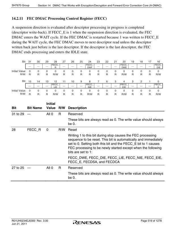
Section 14 DMAC That Works with Encryption/Decryption and Forward Error Correction Core (A-DMAC)
R01UH0234EJ0300 Rev. 3.00 Page 519 of 1278 Jun 21, 2011
SH7670 Group
14.2.11 FEC DMAC Processing Control Register (FECC)
A suspension direction is evaluated after descriptor processing in progress is completed (descriptor write-back). If FECC_E is 1 when the suspension direction is evaluated, the FEC DMAC enters the WAIT cycle. If the FEC DMAC is restarted because 1 was written to FECC_E during the WAIT cycle, the FEC DMAC moves to next descriptor read unless the descriptor written back just before is the last descriptor. If the descriptor is the last descriptor, the FEC DMAC ends processing and enters the IDLE state.
31 30 29 28 27 26 25 24 23 22 21 20 19 18 17 16Bit:
Initial Value:R/W:
Bit:
Initial Value:R/W:
15 14 13 12 11 10 9 8 7 6 5 4 3 2 1 0
0 0 0 0 0 0 0 0 0 0 0 0 0 0 0 0R R R R/W R R R R R R R R/W R R R R/W
0 0 0 0 0 0 0 0 0 0 0 0 0 0 0 0R R R R/W R R R R/W R R R R/W R R R R/W
⎯ ⎯ ⎯FECC_
R ⎯ ⎯ ⎯FECC_DWF ⎯ ⎯ ⎯
FECC_DWE ⎯ ⎯ ⎯
⎯ ⎯ ⎯FECC_
LIE ⎯ ⎯ ⎯ ⎯ ⎯ ⎯FECC_
EIE ⎯ ⎯ ⎯FECC_
EFECC_
NIE
FECC_DIE
Bit Bit Name Initial Value R/W Description
31 to 29 — All 0 R Reserved
These bits are always read as 0. The write value should always be 0.
28 FECC_R 0 R/W Reset
Writing 1 to this bit during stop causes the FEC processing sequence to be reset. This bit is automatically and immediately set to 0. Setting both this bit and the FECC_E bit to 1 causes FEC processing to be newly started except when the following bits are set to 1:
FECC_DWE, FECC_DIE, FECC_LIE, FECC_NIE, FECC_EIE, FECC_E, FECDSA, and FECDCA
27 to 25 — All 0 R Reserved
These bits are always read as 0. The write value should always be 0.

Section 14 DMAC That Works with Encryption/Decryption and Forward Error Correction Core (A-DMAC)
Page 520 of 1278 R01UH0234EJ0300 Rev. 3.00 Jun 21, 2011
SH7670 Group
Bit Bit Name Initial Value R/W Description
24 FECC_DWF
0 R WAIT State Flag after Descriptor Processing End
0: Non-WAIT state
1: WAIT state
There are two methods for understanding the processing state of the FEC DMAC descriptor. In one, when the FEC DMAC is executed, FEC_DWE is set to 1 and then FECC_DIE is set to 1 to accept the "1 descriptor processing end" interrupt request. In the other, the processing state is observed till this bit is set to 1.
23 to 21 — All 0 R Reserved
These bits are always read as 0. The write value should always be 0.
20 FECC_DWE
0 R/W "1 Descriptor Processing End" Interrupt Request Release Wait Enable
When this bit is 1, the FEC DMAC ends processing of this descriptor and enters the WAIT state unless FECC_DIE is 0 after write-back. If the "1 descriptor processing end" interrupt is requested, the FEC DMAC waits for release of the interrupt before it moves to processing of the next descriptor. If this descriptor is the last descriptor when the interrupt is released, the FEC DMAC ends processing and enters the IDLE state. If this descriptor is not the last descriptor, the FEC DMAC reads the next descriptor.
0: The FEC DMAC does not enter the WAIT state when the "1
descriptor processing end" interrupt is requested.
1: The FEC DMAC enters the WAIT state when the "1
descriptor processing end" interrupt is requested.
19 to 17 — All 0 R Reserved
These bits are always read as 0. The write value should always be 0.
16 FECC_DIE 0 R/W "1 Descriptor Processing End" Interrupt Request Enable
Specifies whether to enable or disable the "1 descriptor processing end" interrupt request when processing of this descriptor ends. Processing does not end even if this interrupt is requested. This bit functions as the FECI_DI mask.
0: Disables the "1 descriptor processing end" interrupt request.
1: Enables the "1 descriptor processing end" interrupt request.

Section 14 DMAC That Works with Encryption/Decryption and Forward Error Correction Core (A-DMAC)
R01UH0234EJ0300 Rev. 3.00 Page 521 of 1278 Jun 21, 2011
SH7670 Group
Bit Bit Name Initial Value R/W Description
15 to 13 — All 0 R Reserved
These bits are always read as 0. The write value should always be 0.
12 FECC_LIE 0 R/W "Last Descriptor Processing End" Notification Interrupt Request Enable
Specifies whether to enable or disable the "last descriptor processing end" interrupt request when processing of the last descriptor ends (FECI_LI mask).
0: Disables the "last descriptor processing end" interrupt
request.
1: Enables the "last descriptor processing end" interrupt
request.
11 to 9 — All 0 R Reserved
These bits are always read as 0. The write value should always be 0.
8 FECC_NIE 0 R/W "Invalid Descriptor" Notification Interrupt Request Enable
Specifies whether to enable or disable the "invalid descriptor" notification interrupt request when the invalid descriptor is fetched (FECI_NI mask).
0: Disables the "invalid descriptor" notification interrupt request.
1: Enables the "invalid descriptor" notification interrupt request.
7 to 5 — All 0 R Reserved
These bits are always read as 0. The write value should always be 0.
4 FECC_EIE 0 R/W "Processing End" Interrupt Request Enable
Specifies whether to enable or disable the "processing end" interrupt request when processing ends (FECI_EI mask).
0: Disables the "processing end" interrupt request.
1: Enables the "processing end" interrupt request.
3 to 1 — All 0 R Reserved
These bits are always read as 0. The write value should always be 0.
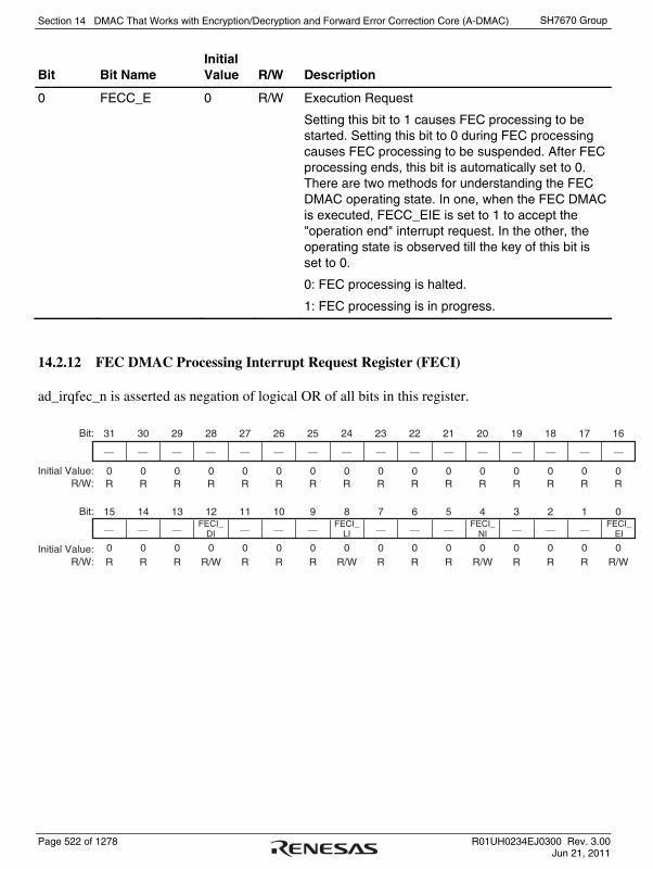
Section 14 DMAC That Works with Encryption/Decryption and Forward Error Correction Core (A-DMAC)
Page 522 of 1278 R01UH0234EJ0300 Rev. 3.00 Jun 21, 2011
SH7670 Group
Bit Bit Name Initial Value R/W Description
0 FECC_E 0 R/W Execution Request
Setting this bit to 1 causes FEC processing to be started. Setting this bit to 0 during FEC processing causes FEC processing to be suspended. After FEC processing ends, this bit is automatically set to 0. There are two methods for understanding the FEC DMAC operating state. In one, when the FEC DMAC is executed, FECC_EIE is set to 1 to accept the "operation end" interrupt request. In the other, the operating state is observed till the key of this bit is set to 0.
0: FEC processing is halted.
1: FEC processing is in progress.
14.2.12 FEC DMAC Processing Interrupt Request Register (FECI)
ad_irqfec_n is asserted as negation of logical OR of all bits in this register.
31 30 29 28 27 26 25 24 23 22 21 20 19 18 17 16Bit:
Initial Value:R/W:
Bit:
Initial Value:R/W:
15 14 13 12 11 10 9 8 7 6 5 4 3 2 1 0
0 0 0 0 0 0 0 0 0 0 0 0 0 0 0 0R R R R R R R R R R R R R R R R
0 0 0 0 0 0 0 0 0 0 0 0 0 0 0 0R R R R/W R R R R/W R R R R/W R R R R/W
⎯ ⎯ ⎯ ⎯ ⎯ ⎯ ⎯ ⎯ ⎯ ⎯ ⎯ ⎯ ⎯ ⎯ ⎯
⎯ ⎯ ⎯FECI_
DI ⎯ ⎯ ⎯FECI_
LI ⎯ ⎯ ⎯FECI_
NI ⎯ ⎯ ⎯
⎯
FECI_EI

Section 14 DMAC That Works with Encryption/Decryption and Forward Error Correction Core (A-DMAC)
R01UH0234EJ0300 Rev. 3.00 Page 523 of 1278 Jun 21, 2011
SH7670 Group
Bit Bit Name Initial Value R/W Description
31 to 13 — All 0 R Reserved
These bits are always read as 0. The write value should always be 0.
12 FECI_DI 0 R/W "1 Descriptor Processing End" Interrupt Notification Request
This interrupt notifies you that the FEC DMAC ended 1 descriptor processing and wrote back the descriptor.
This bit is cleared to 0 by writing 1 to it. When 0 is written to this bit, the current state is retained.
This interrupt is masked by the FECC_DIE bit of the descriptor.
0: The "1 descriptor processing end" interrupt is not
requested.
1: The "1 descriptor processing end" interrupt is
requested.
11 to 9 — All 0 R Reserved
These bits are always read as 0. The write value should always be 0.
8 FECI_LI 0 R/W "Last Descriptor (descriptor where FECD00_F2 is 1) Processing End" Interrupt Notification Request
This interrupt notifies you that the FEC DMAC wrote back the last descriptor and ended last descriptor processing. The FEC DMAC enters the IDLE state after it ended last descriptor processing.
This bit is cleared to 0 by writing 1 to it. When 0 is written to this bit, the current state is retained. If this bit is set, the FEC DMAC is in the initial state because descriptors ran dry. In this case, replenish new descriptors and then restart the FEC DMAC.
This interrupt is masked by the FECC_LIE bit of the FECC.
0: The "last descriptor processing end" interrupt is
not requested.
1: The "last descriptor processing end" interrupt is
requested.

Section 14 DMAC That Works with Encryption/Decryption and Forward Error Correction Core (A-DMAC)
Page 524 of 1278 R01UH0234EJ0300 Rev. 3.00 Jun 21, 2011
SH7670 Group
Bit Bit Name Initial Value R/W Description
7 to 5 — All 0 R Reserved
These bits are always read as 0. The write value should always be 0.
4 FECI_NI 0 R/W "Invalid Descriptor (descriptor where FECD00_F0 is 0) Interrupt
Interrupt request for read end notification. When this interrupt request is made, the FEC DMAC ends processing and enters the IDLE state.
This bit is cleared to 0 by writing 1 to it. When 0 is written to this bit, the current state is retained. This interrupt is masked by the FECC_NIE bit of the FECC. If this bit is set, the FEC DMAC is in the initial state because descriptors ran dry. In this case, replenish new descriptors and then restart the FEC DMAC.
0: The "invalid descriptor processing end" interrupt is
not requested.
1: The "invalid descriptor processing end" interrupt is
requested.
3 to 1 — All 0 R Reserved
These bits are always read as 0. The write value should always be 0.
0 FECI_EI 0 R/W "Processing End" Interrupt Request
This interrupt notifies you that processing ended due to the FECI_LI or FECI_NI interrupt source and the FEC DMAC is now in the IDLE state.
This bit is cleared to 0 by writing 1 to it. When 0 is written to this bit, the current state is retained. This interrupt is masked by the FECC_EIE bit of the FECC.
If this bit is set, the FEC DMAC is in the initial state because descriptors ran dry. In this case, replenish new descriptors and then restart the FEC DMAC.
0: The "processing end" interrupt is not requested.
1: The "processing end" interrupt is requested.

Section 14 DMAC That Works with Encryption/Decryption and Forward Error Correction Core (A-DMAC)
R01UH0234EJ0300 Rev. 3.00 Page 525 of 1278 Jun 21, 2011
SH7670 Group
14.2.13 FEC DMAC Processing Descriptor Start Address Register (FECDSA)
Do not write any value to this register when FECC_E is set to 1.
31 30 29 28 27 26 25 24 23 22 21 20 19 18 17 16Bit:
Initial Value:R/W:
Bit:
Initial Value:R/W:
15 14 13 12 11 10 9 8 7 6 5 4 3 2 1 0
0 0 0 0 0 0 0 0 0 0 0 0 0 0 0 0R/W R/W R/W R/W R/W R/W R/W R/W R/W R/W R/W R/W R/W R/W R/W R/W
0 0 0 0 0 0 0 0 0 0 0 0 0 0 0 0R/W R/W R/W R/W R/W R/W R/W R/W R/W R/W R/W R/W R R R R
FECDSA[3:0]
FECDSA[31:16]
FECDSA[15:4]
Bit Bit Name Initial Value R/W Description
31 to 4 FECDSA[31:4] All 0 R/W
3 to 0 FECDSA[3:0] All 0 R
Descriptor Ring Start Address
Specify a descriptor ring start address. Set a 16-byte boundary address value.

Section 14 DMAC That Works with Encryption/Decryption and Forward Error Correction Core (A-DMAC)
Page 526 of 1278 R01UH0234EJ0300 Rev. 3.00 Jun 21, 2011
SH7670 Group
14.2.14 FEC DMAC Processing Descriptor Current Address Register (FECDCA)
Do not write any value to this register when FECC_E is set to 1.
31 30 29 28 27 26 25 24 23 22 21 20 19 18 17 16Bit:
Initial Value:R/W:
Bit:
Initial Value:R/W:
15 14 13 12 11 10 9 8 7 6 5 4 3 2 1 0
0 0 0 0 0 0 0 0 0 0 0 0 0 0 0 0R/W R/W R/W R/W R/W R/W R/W R/W R/W R/W R/W R/W R/W R/W R/W R/W
0 0 0 0 0 0 0 0 0 0 0 0 0 0 0 0R/W R/W R/W R/W R/W R/W R/W R/W R/W R/W R/W R/W R R R R
FECDCA[3:0]
FECDCA[31:16]
FECDCA[15:4]
Bit Bit Name Initial Value R/W Description
31 to 4 FECDSA[31:4] All 0 R/W
3 to 0 FECDSA[3:0] All 0 R
Descriptor Current Address
Specify the start address of descriptor processing. Set a 16-byte boundary address value. When descriptor processing is in progress, these bits indicate the address of descriptor currently being processed. After descriptor write-back, these bits indicate the address of the next descriptor. When the FEC DMAC enters the IDLE state after it has processed the descriptor where the last flag is set, this register indicates the address of the next descriptor of the descriptor where the last flag is set.
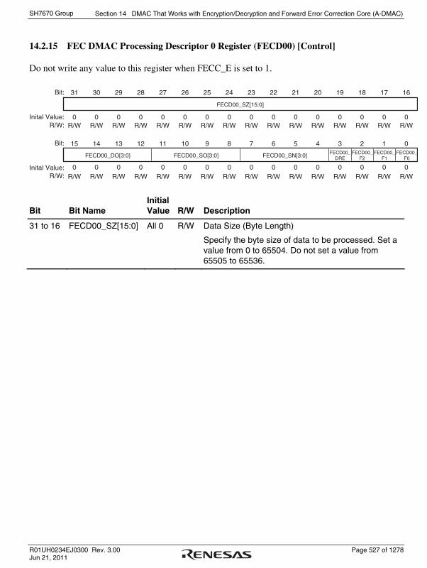
Section 14 DMAC That Works with Encryption/Decryption and Forward Error Correction Core (A-DMAC)
R01UH0234EJ0300 Rev. 3.00 Page 527 of 1278 Jun 21, 2011
SH7670 Group
14.2.15 FEC DMAC Processing Descriptor 0 Register (FECD00) [Control]
Do not write any value to this register when FECC_E is set to 1.
31 30 29 28 27 26 25 24 23 22 21 20 19 18 17 16Bit:
Inital Value:R/W:
Bit:
Inital Value:R/W:
15 14 13 12 11 10 9 8 7 6 5 4 3 2 1 0
0 0 0 0 0 0 0 0 0 0 0 0 0 0 0 0R/W R/W R/W R/W R/W R/W R/W R/W R/W R/W R/W R/W R/W R/W R/W R/W
0 0 0 0 0 0 0 0 0 0 0 0 0 0 0 0R/W R/W R/W R/W R/W R/W R/W R/W R/W R/W R/W R/W R/W R/W R/W R/W
FECD00_SO[3:0] FECD00_SN[3:0] FECD00_DRE
FECD00_F2
FECD00_F1
FECD00_F0FECD00_DO[3:0]
FECD00_SZ[15:0]
Bit Bit Name Initial Value R/W Description
31 to 16 FECD00_SZ[15:0] All 0 R/W Data Size (Byte Length)
Specify the byte size of data to be processed. Set a value from 0 to 65504. Do not set a value from 65505 to 65536.

Section 14 DMAC That Works with Encryption/Decryption and Forward Error Correction Core (A-DMAC)
Page 528 of 1278 R01UH0234EJ0300 Rev. 3.00 Jun 21, 2011
SH7670 Group
Bit Bit Name Initial Value R/W Description
15 to 12 FECD00_DO[3:0] All 0 R/W These bits function when the destination is read or written.
FECD00_DO3:
Data swap in two-byte units (longword swap in word units)
0: As-is 1: Swap
FECD00_DO2:
Data swap in one-byte units (word swap in byte units)
0: As-is 1: Swap
FECD00_DO1:
Inversion of bit 1 at address when one or two bytes are accessed
0: As-is 1: Inversion
FECD00_DO0:
Inversion of bit 0 at address when one byte is accessed
0: As-is 1: Inversion
FECD00_DO1 and FECD00_DO0 function for endian adjustment. Note that if an endian different from the endian of this LSI is used, up to three different addresses are accessed from the address where the start and end addresses are specified when an area is allocated.

Section 14 DMAC That Works with Encryption/Decryption and Forward Error Correction Core (A-DMAC)
R01UH0234EJ0300 Rev. 3.00 Page 529 of 1278 Jun 21, 2011
SH7670 Group
Bit Bit Name Initial Value R/W Description
11 to 8 FECD00_SO[3:0] All 0 R/W These bits function when the source is read.
FECD00_SO3:
Data swap in two-byte units (longword swap in word units)
0: As-is 1: Swap
FECD00_SO2:
Data swap in one-byte units (word swap in byte units)
0: As-is 1: Swap
FECD00_SO1:
Inversion of bit 1 at address when one or two bytes are accessed
0: As-is 1: Inversion
FECD00_SO0:
Inversion of bit 0 at address when one byte is accessed
0: As-is 1: Inversion
FECD00_SO1 and FECD00_SO0 function for endian adjustment. Note that if an endian different from the endian of this LSI is used, up to three different addresses are accessed from the address where the start and end addresses are specified when an area is allocated.
7 to 4 FECD00_SN[3:0] All 0 R/W Number of Source Addresses
Specify the number of source addresses subject to FEC operation.
0000: The number of source addresses is 1.
0001: The number of source addresses is 2.
Others: Reserved (setting prohibited)
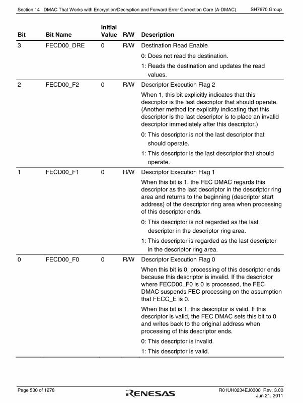
Section 14 DMAC That Works with Encryption/Decryption and Forward Error Correction Core (A-DMAC)
Page 530 of 1278 R01UH0234EJ0300 Rev. 3.00 Jun 21, 2011
SH7670 Group
Bit Bit Name Initial Value R/W Description
3 FECD00_DRE 0 R/W Destination Read Enable
0: Does not read the destination.
1: Reads the destination and updates the read
values.
2 FECD00_F2 0 R/W Descriptor Execution Flag 2
When 1, this bit explicitly indicates that this descriptor is the last descriptor that should operate. (Another method for explicitly indicating that this descriptor is the last descriptor is to place an invalid descriptor immediately after this descriptor.)
0: This descriptor is not the last descriptor that
should operate.
1: This descriptor is the last descriptor that should
operate.
1 FECD00_F1 0 R/W Descriptor Execution Flag 1
When this bit is 1, the FEC DMAC regards this descriptor as the last descriptor in the descriptor ring area and returns to the beginning (descriptor start address) of the descriptor ring area when processing of this descriptor ends.
0: This descriptor is not regarded as the last
descriptor in the descriptor ring area.
1: This descriptor is regarded as the last descriptor
in the descriptor ring area.
0 FECD00_F0 0 R/W Descriptor Execution Flag 0
When this bit is 0, processing of this descriptor ends because this descriptor is invalid. If the descriptor where FECD00_F0 is 0 is processed, the FEC DMAC suspends FEC processing on the assumption that FECC_E is 0.
When this bit is 1, this descriptor is valid. If this descriptor is valid, the FEC DMAC sets this bit to 0 and writes back to the original address when processing of this descriptor ends.
0: This descriptor is invalid.
1: This descriptor is valid.

Section 14 DMAC That Works with Encryption/Decryption and Forward Error Correction Core (A-DMAC)
R01UH0234EJ0300 Rev. 3.00 Page 531 of 1278 Jun 21, 2011
SH7670 Group
14.2.16 FEC DMAC Processing Descriptor 1 Register (FECD01D0A) [Destination
Address]
Do not write any value to this register when FECC_E is set to 1.
31 30 29 28 27 26 25 24 23 22 21 20 19 18 17 16Bit:
Initial Value:R/W:
Bit:
Initial Value:R/W:
15 14 13 12 11 10 9 8 7 6 5 4 3 2 1 0
0 0 0 0 0 0 0 0 0 0 0 0 0 0 0 0R/W R/W R/W R/W R/W R/W R/W R/W R/W R/W R/W R/W R/W R/W R/W R/W
0 0 0 0 0 0 0 0 0 0 0 0 0 0 0 0R/W R/W R/W R/W R/W R/W R/W R/W R/W R/W R/W R/W R/W R/W R/W R/W
FECD01D0A[31:16]
FECD01D0A[15:0]
Bit Bit Name Initial Value R/W Description
31 to 0 FECD01D0A[31:0] All 0 R/W Destination Address
Specify a processing data write-back destination address.
14.2.17 FEC DMAC Processing Descriptor 2 Register (FECD02S0A) [Source 0 Address]
Do not write any value to this register when FECC_E is set to 1.
31 30 29 28 27 26 25 24 23 22 21 20 19 18 17 16Bit:
Initial Value:R/W:
Bit:
Initial Value:R/W:
15 14 13 12 11 10 9 8 7 6 5 4 3 2 1 0
0 0 0 0 0 0 0 0 0 0 0 0 0 0 0 0R/W R/W R/W R/W R/W R/W R/W R/W R/W R/W R/W R/W R/W R/W R/W R/W
0 0 0 0 0 0 0 0 0 0 0 0 0 0 0 0R/W R/W R/W R/W R/W R/W R/W R/W R/W R/W R/W R/W R/W R/W R/W R/W
FECD02S0A[31:16]
FECD02S0A[15:0]
Bit Bit Name Initial Value R/W Description
31 to 0 FECD02S0A[31:0] All 0 R/W Specify the start address of source 0 data.
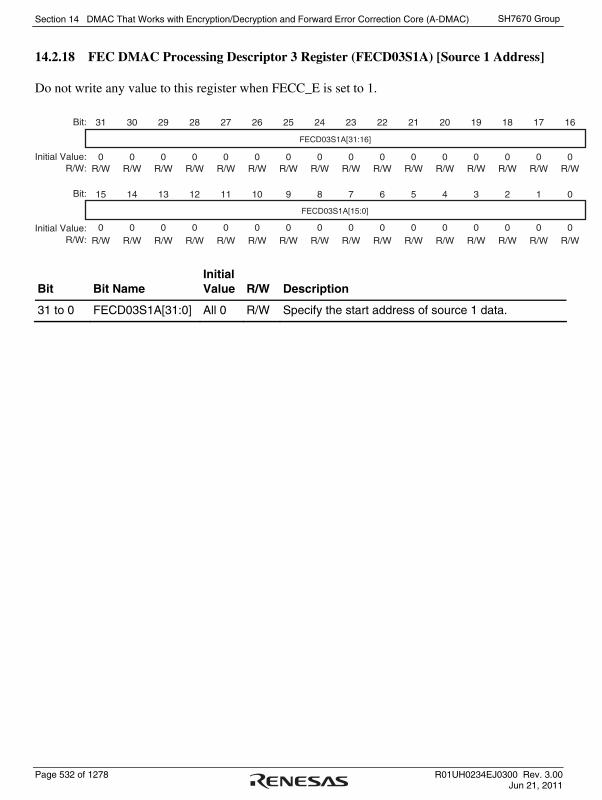
Section 14 DMAC That Works with Encryption/Decryption and Forward Error Correction Core (A-DMAC)
Page 532 of 1278 R01UH0234EJ0300 Rev. 3.00 Jun 21, 2011
SH7670 Group
14.2.18 FEC DMAC Processing Descriptor 3 Register (FECD03S1A) [Source 1 Address]
Do not write any value to this register when FECC_E is set to 1.
31 30 29 28 27 26 25 24 23 22 21 20 19 18 17 16Bit:
Initial Value:R/W:
Bit:
Initial Value:R/W:
15 14 13 12 11 10 9 8 7 6 5 4 3 2 1 0
0 0 0 0 0 0 0 0 0 0 0 0 0 0 0 0R/W R/W R/W R/W R/W R/W R/W R/W R/W R/W R/W R/W R/W R/W R/W R/W
0 0 0 0 0 0 0 0 0 0 0 0 0 0 0 0R/W R/W R/W R/W R/W R/W R/W R/W R/W R/W R/W R/W R/W R/W R/W R/W
FECD03S1A[31:16]
FECD03S1A[15:0]
Bit Bit Name Initial Value R/W Description
31 to 0 FECD03S1A[31:0] All 0 R/W Specify the start address of source 1 data.

Section 14 DMAC That Works with Encryption/Decryption and Forward Error Correction Core (A-DMAC)
R01UH0234EJ0300 Rev. 3.00 Page 533 of 1278 Jun 21, 2011
SH7670 Group
14.3 Functions
Table 14.2 lists A-DMAC security/network functions.
Table 14.2 A-DMAC Security/Network Functions
Classification Item Description Conforming/ Supported Standard
Error detection Checksum • 1's complement sum operation RFC1071 support
Error correction FEC • FEC XOR operation
• Support of any number of FEC
matrixes
RFC2733
Pro-MPEG support

Section 14 DMAC That Works with Encryption/Decryption and Forward Error Correction Core (A-DMAC)
Page 534 of 1278 R01UH0234EJ0300 Rev. 3.00 Jun 21, 2011
SH7670 Group
14.3.1 DMAC Channel Function
The A-DMAC has two DMAC channels for checksum processing.
14.3.2 Checksum
Checksum is a data error detection scheme. Checksum splits the entered data in 16-bit units and calculates their 1's complement sum to detect an error. For example, TCP checksum used to detect packet errors on the receiving side splits information called an IP pseudo header, TCP header, and TCP payload data in 16-bit units and calculates their 1's complement sum. If the obtained 1's complement sum is H'FFFF or H'0000, it indicates that no packet error occurred. If the 1's complement sum is not H'FFFF and H'0000, it indicates that a packet error occurred.
The A-DMAC has a function to calculate the 1's complement sum of data obtained via DMA transfer.
14.3.3 FEC Channel
The A-DMAC has one channel for FEC operation. This channel can perform XOR operation for the data obtained via DMA transfer and write back to memory because it is of a descriptor structure that can cope with FEC operation of any number of rows.

Section 14 DMAC That Works with Encryption/Decryption and Forward Error Correction Core (A-DMAC)
R01UH0234EJ0300 Rev. 3.00 Page 535 of 1278 Jun 21, 2011
SH7670 Group
14.3.4 FEC Operation
FEC is an error correction method. This method enables the receiving side to repair the lost packet without requesting packet retransmission. When repairing the lost packet by using FEC, the transmitting side uses the original packet group to generate a redundant packet (FEC packet). When transmitting 100 packets, for example, the transmitting side generates a 10 x 10 packet matrix, XORs the ten original packets aligned to one row or column, and generates one FEC packet per row (column). In this example, 20 FEC packets are generated. The transmitting side transmits the original data packet group and FEC packets to the receiving side. To check whether the original packets are lost, the receiving side aligns the original packets and FEC packets to the matrix as in the transmitting side. If a lost original packet is found, the transmitting side can repair the packet by XORing the other packets in the row and column to which the lost packet belongs with the FEC packets. Like this, the transmitting side and receiving side need to share the number of rows and columns of matrix aligned to generate FEC packets before transmitting and receiving the packets.
The A-DMAC has the XOR calculation function used for FEC operation and supports the following FEC specifications of RFC2733 and Pro-MPEG:
• XOR calculation of any number of rows (columns)
A variable-length descriptor supports the FEC structure of theoretically infinite length.
• One-dimensional FEC
Not only two-dimensional FEC but also one-dimensional FEC is supported because processing is performed per row (column).
The CPU must perform the following operations:
• FEC matrix alignment
• Lost packet detection
• Unification of the lengths of packets that constitute a row (column)
(Packets less than the maximum packet length are padded with 0.)
• Repair of a portion of timestamp and payload type from the result obtained from the A-DMAC

Section 14 DMAC That Works with Encryption/Decryption and Forward Error Correction Core (A-DMAC)
Page 536 of 1278 R01UH0234EJ0300 Rev. 3.00 Jun 21, 2011
SH7670 Group
14.4 Channel Operation
14.4.1 Descriptor Format
The A-DMAC can automatically perform DMA transfer between memory and the STIF without the CPU based on the descriptor containing information such as a buffer pointer and its data size. The A-DMAC automatically performs operations such as reading data from memory and writing the decrypted data to the STIF according to the information stored in this descriptor.
Figure 14.2 shows the descriptor format. The gray parts in the figure are ignored when descriptor processing is started and "0" is written back to these parts after descriptor processing ends. For details on each bit, see section 14.2.6, Channel [i] Processing Descriptor 0 Register (C[i]D0) [Control] (i = 0, 1), to section 14.2.10, Channel [i] Processing Descriptor 4 Register (C[i]D4) [Checksum Value Write Address] (i = 0, 1).
31
0 CRDO[3:0]
AddressBit
CHDO[3:0] SO[3:0] DA SA
D1 [31:0]
D4 [31:1]
D2 [31:0]
CSM[1:0] F[2:0]
+4
+8
+12
+16
+20
+24
+28
30 29 28
DWE DIE D3 [15:0]
27-26 25-24 23-20 17-16 15-3 2-1 019 18
Figure 14.2 Descriptor Format
A descriptor is 16/32-byte variable length or 32-byte fixed length. Select variable length or fixed length from the variable-length descriptor control flag (C[i]C_VLD) of the channel [i] processing control register (C[i]C). If C[i]C_VLD is set to 1 to operate the descriptor as the variable-length descriptor, the remaining 16 bytes are read when the following conditions are met:
• Checksum calculation result write-back is set (C[i]CSM0 = 1).
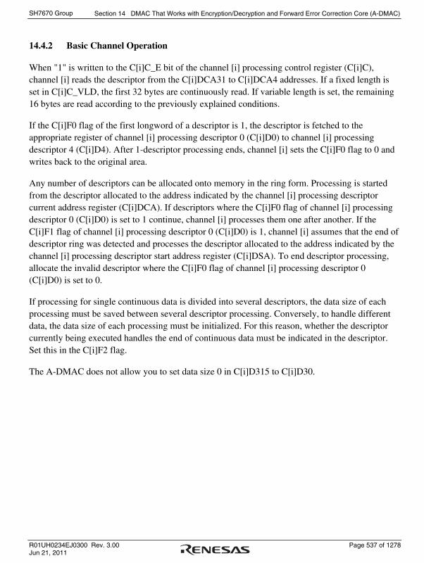
Section 14 DMAC That Works with Encryption/Decryption and Forward Error Correction Core (A-DMAC)
R01UH0234EJ0300 Rev. 3.00 Page 537 of 1278 Jun 21, 2011
SH7670 Group
14.4.2 Basic Channel Operation
When "1" is written to the C[i]C_E bit of the channel [i] processing control register (C[i]C), channel [i] reads the descriptor from the C[i]DCA31 to C[i]DCA4 addresses. If a fixed length is set in C[i]C_VLD, the first 32 bytes are continuously read. If variable length is set, the remaining 16 bytes are read according to the previously explained conditions.
If the C[i]F0 flag of the first longword of a descriptor is 1, the descriptor is fetched to the appropriate register of channel [i] processing descriptor 0 (C[i]D0) to channel [i] processing descriptor 4 (C[i]D4). After 1-descriptor processing ends, channel [i] sets the C[i]F0 flag to 0 and writes back to the original area.
Any number of descriptors can be allocated onto memory in the ring form. Processing is started from the descriptor allocated to the address indicated by the channel [i] processing descriptor current address register (C[i]DCA). If descriptors where the C[i]F0 flag of channel [i] processing descriptor 0 (C[i]D0) is set to 1 continue, channel [i] processes them one after another. If the C[i]F1 flag of channel [i] processing descriptor 0 (C[i]D0) is 1, channel [i] assumes that the end of descriptor ring was detected and processes the descriptor allocated to the address indicated by the channel [i] processing descriptor start address register (C[i]DSA). To end descriptor processing, allocate the invalid descriptor where the C[i]F0 flag of channel [i] processing descriptor 0 (C[i]D0) is set to 0.
If processing for single continuous data is divided into several descriptors, the data size of each processing must be saved between several descriptor processing. Conversely, to handle different data, the data size of each processing must be initialized. For this reason, whether the descriptor currently being executed handles the end of continuous data must be indicated in the descriptor. Set this in the C[i]F2 flag.
The A-DMAC does not allow you to set data size 0 in C[i]D315 to C[i]D30.

Section 14 DMAC That Works with Encryption/Decryption and Forward Error Correction Core (A-DMAC)
Page 538 of 1278 R01UH0234EJ0300 Rev. 3.00 Jun 21, 2011
SH7670 Group
14.4.3 Checksum
Figure 14.3 shows an example of descriptors that execute only checksum. In figure 14.3, (a) is an example of continuously allocating checksum descriptors each of which completes one processing and (b) is an example of splitting processing into several checksum descriptors and allocating the last checksum descriptor that completes processing.
In the descriptor that performs checksum operation, set the data size in multiples of two bytes. However, if split descriptors are used, a value other than a multiple of two bytes can be set as the data size in each descriptor but the total number of data sizes specified in the split descriptors must be set so that it becomes a multiple of 2. (If processing is split into several descriptors and an odd size is specified in the non-last descriptor, the A-DMAC waits for the next descriptor without processing data of the last one byte.)

Section 14 DMAC That Works with Encryption/Decryption and Forward Error Correction Core (A-DMAC)
R01UH0234EJ0300 Rev. 3.00 Page 539 of 1278 Jun 21, 2011
SH7670 Group
Checksum descriptorC[i]CSM[1:0] = H'3C[i]CM[6:0] = H'7fC[i]HM[4:0] = H'1fC[i]F2 = 1C[i]F0 = 1
Checksum descriptorC[i]CSM[1:0] = H'3C[i]CM[6:0] = H'7fC[i]HM[4:0] = H'1fC[i]F2 = 1C[i]F0 = 1
Invalid descriptorC[i]CSM[1:0] = ANYC[i]CM[6:0] = ANYC[i]HM[4:0] = ANYC[i]F2 = ANYC[i]F0 = 0
Checksum descriptorC[i]CSM[1:0] = H'2C[i]CM[6:0] = H'7fC[i]HM[4:0] = H'1fC[i]F2 = 0C[i]F0 = 1
(a) Example of continuously allocating checksum descriptors each of which completes one processing
(b) Example of splitting processing into several checksum descriptors and allocating the last checksum descriptor that completes processing
Checksum descriptorC[i]CSM[1:0] = H'0C[i]CM[6:0] = H'7fC[i]HM[4:0] = H'1fC[i]F2 = 0C[i]F0 = 1
Checksum descriptorC[i]CSM[1:0] = H'1C[i]CM[6:0] = H'7fC[i]HM[4:0] = H'1fC[i]F2 = 1C[i]F0 = 1
Invalid descriptorC[i]CSM[1:0] = ANYC[i]CM[6:0] = ANYC[i]HM[4:0] = ANYC[i]F2 = ANYC[i]F0 = 0
Figure 14.3 Examples of Allocating Checksum Descriptors

Section 14 DMAC That Works with Encryption/Decryption and Forward Error Correction Core (A-DMAC)
Page 540 of 1278 R01UH0234EJ0300 Rev. 3.00 Jun 21, 2011
SH7670 Group
14.5 FEC Channel Operation
14.5.1 Descriptor Format for FEC Channel
Figure 14.4 shows the descriptor format for the FEC channel. The FEC channel can automatically perform DMA transfer with memory without the CPU according to descriptor information.
Two source addresses can be specified in a descriptor but linking descriptors in the ring form provides FEC processing of any number of rows (columns).
Only I-BUS can access FEC channel data due to its application, so information indicating the source and destination directions (I-BUS or STIF) is not included in the descriptor. The size of data subject to FEC operation must match the data size set in the FECD0_SZ15 to FECD0_SZ0 flag of FEC DMAC processing descriptor 0 (FECD00) in the first longword of the FEC descriptor. For this reason, when processing data less than the data size set in the FECD0_SZ15 to FECD0_SZ0 flag, you must pad the data with 0 and perform FEC processing.
31-16
0 SZ[15:0]
AddressBit
DO[3:0] SN[3:0]SO[3:0] DRE F[2:0]
D01D0A [31:0]
D02S0A [31:0]
D03S1A [31:0] or padding
+4
+8
+12
15-12 11-8 7-4 3 2-0
Figure 14.4 FEC DMAC Descriptor Format

Section 14 DMAC That Works with Encryption/Decryption and Forward Error Correction Core (A-DMAC)
R01UH0234EJ0300 Rev. 3.00 Page 541 of 1278 Jun 21, 2011
SH7670 Group
14.5.2 Basic FEC Channel Operation
When "1" is written to the FECC_E bit of the FEC DMAC processing control register (FECC), the FEC channel starts descriptor read. If the FECD00_F0 flag in the first longword is "1", descriptors are fetched in turn to the appropriate register, starting from FECD00 in the first longword.
After descriptor read is completed, the FEC channel reads data from memory space indicated by a source address and performs FEC operation (XOR calculation). After XOR calculation with all source addresses is completed, the FEC channel writes back the result to destination address space. After 1-descriptor processing ends, the FEC channel sets the FECD00_F0 flag to "0" and writes back to the original area.
To support the FEC matrix operation of any number of rows and columns, the FEC channel installed on the A-DMAC temporarily writes back the FEC operation result of source rows/columns that can be processed by one descriptor to the destination address. If the FEC matrix consists of two rows, the FEC matrix operation ends in one descriptor. If the FEC matrix consists of 3 rows/columns or more, the FEC channel splits the matrix into several descriptors and performs FEC matrix processing. If this processing must be split into several descriptors, use the FECD00_DRE bit to control the FEC operation.
Figure 14.5 shows an example of descriptor configuration where the FEC matrix operation is split into several descriptors for execution. In the first descriptor that starts the FEC operation, FECD00_DRE is set to 0 because the operation result is not yet written. In the second and subsequent descriptors, the FEC operation is continued. In other words, to XOR the calculation result of the previous descriptor with the current descriptor source, FECD00_DRE is set to 1. Piling up such descriptors till the number of rows or columns for the FEC matrix operation is met makes it possible to obtain the last XOR operation result of the target row (column).
Any number of descriptors can be allocated onto memory in the ring form. Processing is started from the descriptor allocated to the address indicated by the FEC DMAC processing descriptor current address register (FECDCA). If descriptors where the FECD00_F0 flag of FEC DMAC processing descriptor 0 (FECD00) is set to 1 continue, the FEC channel processes them one after another. If the FECD00_F1 flag of FECD00 is 1, the FEC channel assumes that the end of descriptor ring was detected and processes the descriptor allocated to the address indicated by the FEC DMAC processing descriptor start address register (FECDSA). To end descriptor processing, allocate the invalid descriptor where the FECD00_F0 flag of FECD00 is set to "0" or allocate the last descriptor where the FECD00_F2 flag of FECD00 is set to "1".
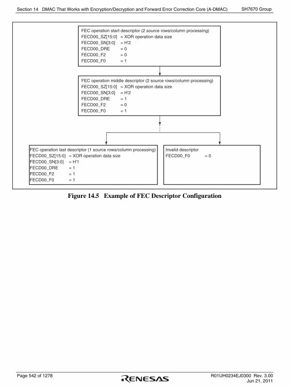
Section 14 DMAC That Works with Encryption/Decryption and Forward Error Correction Core (A-DMAC)
Page 542 of 1278 R01UH0234EJ0300 Rev. 3.00 Jun 21, 2011
SH7670 Group
FEC operation last descriptor (1 source rows/column processing)FECD00_SZ[15:0] = XOR operation data sizeFECD00_SN[3:0] = H'1FECD00_DRE = 1FECD00_F2 = 1FECD00_F0 = 1
Invalid descriptorFECD00_F0 = 0
FEC operation middle descriptor (2 source rows/column processing)FECD00_SZ[15:0] = XOR operation data sizeFECD00_SN[3:0] = H'2FECD00_DRE = 1FECD00_F2 = 0FECD00_F0 = 1
FEC operation start descriptor (2 source rows/column processing)FECD00_SZ[15:0] = XOR operation data sizeFECD00_SN[3:0] = H'2FECD00_DRE = 0FECD00_F2 = 0FECD00_F0 = 1
Figure 14.5 Example of FEC Descriptor Configuration

Section 14 DMAC That Works with Encryption/Decryption and Forward Error Correction Core (A-DMAC)
R01UH0234EJ0300 Rev. 3.00 Page 543 of 1278 Jun 21, 2011
SH7670 Group
14.6 Usage Notes
14.6.1 Data Transfer Size Set in Descriptor for A-DMAC Channel Operation
The data transfer size to be set in a descriptor for A-DMAC channel operation is as explained in the description of the C[i]D3[15:0] bits in section 14.2.9, Channel [i] Processing Descriptor 3 Register (C[i]D3) [Data Length] (i = 0, 1). Note however that the following restrictions are applied when the relevant A-DMAC channel is operating together with an STIF in PS mode.
When operating together with an STIF in PS mode, a descriptor for dummy data transfer must be prepared to satisfy the expression of (data transfer size specified by A-DMAC descriptor) = (setting of the SIZE[31:0] bits in STSIZER) + dummy data = multiple of 192 bytes. This means that the sum of the C[i]D3[15:0] bits for each descriptor should be a multiple of 192 bytes when data transfer is divided to be performed by multiple descriptors.
Accordingly, in PS output mode, data including dummy data is transferred from the A-DMAC to the STIF, but the dummy data is deleted inside the STIF and only the data that should really be transferred will be output from the STIF to an external device.
Similarly, in PS input mode, the STIF retrieves only the amount of data that should really be transferred from an external device. However, the A-DMAC transfers the data that should really be transferred followed by dummy data. Software should ignore the dummy data stored in memory.

Section 14 DMAC That Works with Encryption/Decryption and Forward Error Correction Core (A-DMAC)
Page 544 of 1278 R01UH0234EJ0300 Rev. 3.00 Jun 21, 2011
SH7670 Group
Section 15 Stream Interface (STIF)
R01UH0234EJ0300 Rev. 3.00 Page 545 of 1278 Jun 21, 2011
SH7670 Group
Section 15 Stream Interface (STIF)
This LSI has a 2-channel stream interface (STIF).
15.1 Features
• Two-channel bidirectional interface
• Supports TS packets (packet size: 188 bytes).
• Supports TTS packets (packet size: 192 bytes).
• Supports PS packets (packet size: specified by the size register).
• 8-bit parallel transfer or 1-bit serial transfer is selectable.
• Transfer direction is settable for each channel.
• Polarity of each clock signal, request signal, synchronizing signal, and data enable signal is selectable.
• A PCR clock recovery module (PCRRCV) incorporated

Section 15 Stream Interface (STIF)
Page 546 of 1278 R01UH0234EJ0300 Rev. 3.00 Jun 21, 2011
SH7670 Group
Figure 15.1 shows a block diagram of the STIF.
Internal bus 32-bit width synchronize with Bφ
A-DMAC
Transmit buffer
Receive buffer
Transmit buffer
Receive buffer
Stream controller Stream controller
Dat
a cl
ock
outp
ut
ST0_CLKIN
ST0_REQ
ST0_SYC
ST0_VLD
ST0_D[7:0]
ST0_VCO_CLKIN
ST0_PWM
ST1_CLKIN
ST1_REQ
ST1_SYC
ST1_VLD
ST1_D[7:0]
ST1_VCO_CLKIN
ST1_PWM
ST_CLKOUT
STIF
Figure 15.1 Block Diagram of STIF
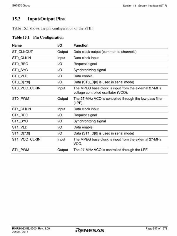
Section 15 Stream Interface (STIF)
R01UH0234EJ0300 Rev. 3.00 Page 547 of 1278 Jun 21, 2011
SH7670 Group
15.2 Input/Output Pins
Table 15.1 shows the pin configuration of the STIF.
Table 15.1 Pin Configuration
Name I/O Function
ST_CLKOUT Output Data clock output (common to channels)
ST0_CLKIN Input Data clock input
ST0_REQ I/O Request signal
ST0_SYC I/O Synchronizing signal
ST0_VLD I/O Data enable
ST0_D[7:0] I/O Data (ST0_D[0] is used in serial mode)
ST0_VCO_CLKIN Input The MPEG base clock is input from the external 27-MHz voltage controlled oscillator (VCO).
ST0_PWM Output The 27-MHz VCO is controlled through the low-pass filter (LPF).
ST1_CLKIN Input Data clock input
ST1_REQ I/O Request signal
ST1_SYC I/O Synchronizing signal
ST1_VLD I/O Data enable
ST1_D[7:0] I/O Data (ST1_D[0] is used in serial mode)
ST1_VCO_CLKIN Input The MPEG base clock is input from the external 27-MHz VCO.
ST1_PWM Output The 27-MHz VCO is controlled through the LPF.
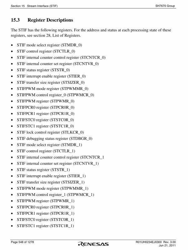
Section 15 Stream Interface (STIF)
Page 548 of 1278 R01UH0234EJ0300 Rev. 3.00 Jun 21, 2011
SH7670 Group
15.3 Register Descriptions
The STIF has the following registers. For the address and status at each processing state of these registers, see section 28, List of Registers.
• STIF mode select register (STMDR_0)
• STIF control register (STCTLR_0)
• STIF internal counter control register (STCNTCR_0)
• STIF internal counter set register (STCNTVR_0)
• STIF status register (STSTR_0)
• STIF interrupt enable register (STIER_0)
• STIF transfer size register (STSIZER_0)
• STIFPWM mode register (STPWMMR_0)
• STIFPWM control register_0 (STPWMCR_0)
• STIFPWM register (STPWMR_0)
• STIFPCR0 register (STPCR0R_0)
• STIFPCR1 register (STPCR1R_0)
• STIFSTC0 register (STSTC0R_0)
• STIFSTC1 register (STSTC1R_0)
• STIF lock control register (STLKCR_0)
• STIF debugging status register (STDBGR_0)
• STIF mode select register (STMDR_1)
• STIF control register (STCTLR_1)
• STIF internal counter control register (STCNTCR_1
• STIF internal counter set register (STCNTVR_1)
• STIF status register (STSTR_1)
• STIF interrupt enable register (STIER_1)
• STIF transfer size register (STSIZER_1)
• STIFPWM mode register (STPWMMR_1)
• STIFPWM control register_1 (STPWMCR_1)
• STIFPWM register (STPWMR_1)
• STIFPCR0 register (STPCR0R_1)
• STIFPCR1 register (STPCR1R_1)
• STIFSTC0 register (STSTC0R_1)
• STIFSTC1 register (STSTC1R_1)

Section 15 Stream Interface (STIF)
R01UH0234EJ0300 Rev. 3.00 Page 549 of 1278 Jun 21, 2011
SH7670 Group
• STIF lock control register (STLKCR_1)
• STIF debugging status register (STDBGR_1)
15.3.1 STIF Mode Select Register (STMDR)
STMDR is a 32-bit register that selects operating mode, clock source, etc. of the on-chip STIF module. STMDR is initialized to H'00000000 by a power-on reset.
Bit Bit Name Initial Value R/W Description
31 to 15 ⎯ All 0 R Reserved
These bits are always read as 0. The write value should always be 0.
14 LSBSEL 0 R/W Selects MSB first or LSB first in serial mode.
0: MSB-first data input/output
1: LSB-first data input/output
13 EDGSEL 0 R/W Selects input/output timing of STn_REQ, STn_SYC, STn_VLD, and STn_D[7:0].
0: Output and sampled at the rising edge of the synchronizing clock
1: Output and sampled at the falling edge of the synchronizing clock
The synchronizing clock is defined by the CLKSEL and CKFRSEL[3:0] bits in this register.
12 CLKSEL 0 R/W Selects synchronizing clock for stream transmit mode
0: STn_SYC, STn_VLD, and STn_D[7:0] are output in synchronization with ST_CLKOUT.
STn_REQ is sampled in synchronization with ST_CLKOUT
1: STn_SYC, STn_VLD, and STn_D[7:0] are output in synchronization with STn_CLKIN.
STn_REQ is sampled in synchronization with STn_CLKIN.

Section 15 Stream Interface (STIF)
Page 550 of 1278 R01UH0234EJ0300 Rev. 3.00 Jun 21, 2011
SH7670 Group
Bit Bit Name Initial Value R/W Description
11
10
9
8
CKFRSEL3
CKFRSEL2
CKFRSEL1
CKFRSEL0
0
0
0
0
R/W
R/W
R/W
R/W
These bits select the clock source of ST_CLKOUT (available for STMDR_0 only).
0000: Bφ
0001: Iφ/2
0010: Iφ/3
0011: Iφ/4
0100: Iφ/6
0101: Iφ/8
0110: Iφ/12
0111: Reserved (setting prohibited)
1000: Reserved (setting prohibited)
1001: Reserved (setting prohibited)
1010: Reserved (setting prohibited)
1011: Reserved (setting prohibited)
1100: Reserved (setting prohibited)
1101: Reserved (setting prohibited)
1110: Reserved (setting prohibited)
1111: Output is fixed to low.
Notes: 1. For serial mode, select a clock source of Bφ or less. For parallel mode, select a clock source of Bφ/2 or less.
For example, when Iφ : Bφ = 3 : 1 or 6 : 2 is set in the CPG, Iφ/2 is not selectable for serial mode. For parallel mode, Iφ/2 and Iφ/4 are not selectable.
2. Select a clock source that satisfies the following: STn_CLKIN ≤ Bφ × 80% (serial mode)
STn_CLKIN ≤ (Bφ/2) × 80% (parallel mode)
7 REQACTSEL 0 R/W Selects the active polarity of STn_REQ.
0: Active-high
1: Active-low

Section 15 Stream Interface (STIF)
R01UH0234EJ0300 Rev. 3.00 Page 551 of 1278 Jun 21, 2011
SH7670 Group
Bit Bit Name Initial Value R/W Description
6 VLDACTSEL 0 R/W Selects the active polarity of STn_VLD.
0: Active-high
1: Active-low
5 SYCACTSEL 0 R/W Selects the active polarity of STn_SYC.
0: Active-high
1: Active-low
4 IOSEL 0 R/W Selects stream input or output direction.
0: Input (from an external device to this LSI)
1: Output (from this LSI to an external device)
3
2
1
0
IFMDSEL3
IFMDSEL2
IFMDSEL1
IFMDSEL0
0
0
0
0
R/W
R/W
R/W
R/W
These bits select operating mode.
0000: TS serial mode 1
0001: TS parallel mode 1
0010: TS serial mode 2
0011: TS parallel mode 2
0100: TS serial mode 3
0101: TS parallel mode 3
0110: Reserved (setting prohibited)
0111: Reserved (setting prohibited)
1000: TTS serial mode
1001: TTS parallel mode
1010: Reserved (setting prohibited)
1011: Reserved (setting prohibited)
1100: PS serial mode
1101: PS parallel mode
1110: Reserved (setting prohibited)
1111: Reserved (setting prohibited)
[Legend] n = 0, 1

Section 15 Stream Interface (STIF)
Page 552 of 1278 R01UH0234EJ0300 Rev. 3.00 Jun 21, 2011
SH7670 Group
15.3.2 STIF Control Register (STCTLR)
STCTLR is a 32-bit register that sets the recovery processing switching threshold value and enables/disables DMA transfer requests. STCTLR is initialized to H'00000000 by a power-on reset.
Bit Bit Name Initial Value R/W Description
31 to 12 ⎯ All 0 R Reserved
These bits are always read as 0. The write value should always be 0.
11
10
9
RCVTM2
RCVTM1
RCVTM0
0
0
0
R/W
R/W
R/W
These bits set the recovery processing switching threshold value for packet output in TS mode 1 or TS mode 2. These bits are valid when RCV = 1.
000: Approximately 0.625 seconds
001: Approximately 1.25 seconds
010: Approximately 2.5 seconds
011: Approximately 5 seconds
100: Approximately 10 seconds
101: Approximately 20 seconds
110: Approximately 40 seconds
111: Approximately 80 seconds
The recovery functions are processed as follows:
Recovery function (1)
When the internal counter value exceeds the timestamp value and the difference is smaller than the set threshold value, the packet is output immediately.
Recovery function (2)
When the internal counter value exceeds the timestamp value and the difference is larger than the set threshold value, the packet is discarded and the recovery processing restarts with the next packet. (The next packet is output immediately, and the packet's timestamp is reloaded to the internal counter for timestamp at the same time.)
Recovery function (3)
When the internal counter value is under the timestamp value but the difference is larger than the set threshold value, the packet is discarded and the recovery processing restarts with the next packet. (The next packet is output immediately, and the packet's timestamp is reloaded to the internal counter for timestamp at the same time.)

Section 15 Stream Interface (STIF)
R01UH0234EJ0300 Rev. 3.00 Page 553 of 1278 Jun 21, 2011
SH7670 Group
Bit Bit Name Initial Value R/W Description
8 RCV 0 R/W Enables the recovery functions when outputting packets in TS mode 1 or TS mode 2.
0: Recovery functions disabled
1: Recovery functions enabled
7 TRICK 0 R/W Enables the function that transfers stream independently of timestamp when outputting packets in TS mode 1 or TS mode 2.
0: Transfer function disabled
1: Transfer function enabled
6 to 3 ⎯ All 0 R Reserved
These bits are always read as 0. The write value should always be 0.
2 REQEN 0 R/W Enables or disables DMA transfer requests to the A-DMAC.
0: Disabled
1: Enabled
1 EN 0 R/W Enables or disables stream input/output.
0: Disabled
1: Enabled
0 SRST 0 R/W Setting this bit to 1 causes the internal state of this LSI to be initialized with register settings retained.
When a TS packet is received for the first time after the initialization, the timestamp value of the TS packet is reloaded to the internal counter for timestamp.
While 1 is read from this bit, the initialization is in progress.
This bit is automatically cleared to 0.
Whenever the STMDR setting is modified, be sure to set SRST to 1 to initialize this LSI and then set EN and REQEN to 1 to enable stream transfer.

Section 15 Stream Interface (STIF)
Page 554 of 1278 R01UH0234EJ0300 Rev. 3.00 Jun 21, 2011
SH7670 Group
15.3.3 STIF Internal Counter Control Register (STCNTCR)
STCNTCR is a 32-bit register to control the internal counter for timestamp. STCNTCR is initialized to H'00000000 by a power-on reset.
Bit Bit Name Initial Value R/W Description
31 to 4 ⎯ All 0 R Reserved
These bits are always read as 0. The write value should always be 0.
3 CRD 0 R/W Setting this bit to 1 causes the internal counter value for timestamp to be read to STCNTVR.
This bit is automatically cleared to 0.
2 CSTP 0 R/W Stops the internal counter for timestamp.
0: Count operation is continued.
1: Counter is stopped with its value retained.
1 CSET 0 R/W Setting this bit to 1 causes the STCNTVR value to be reloaded to the internal counter for timestamp.
This bit is automatically cleared to 0.
0 CRST 0 R/W Setting this bit to 1 causes the internal counter for timestamp to be initialized to H'00000000.
This bit is automatically cleared to 0.
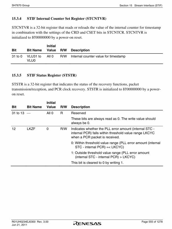
Section 15 Stream Interface (STIF)
R01UH0234EJ0300 Rev. 3.00 Page 555 of 1278 Jun 21, 2011
SH7670 Group
15.3.4 STIF Internal Counter Set Register (STCNTVR)
STCNTVR is a 32-bit register that reads or reloads the value of the internal counter for timestamp in combination with the settings of the CRD and CSET bits in STCNTCR. STCNTVR is initialized to H'00000000 by a power-on reset.
Bit Bit Name Initial Value R/W Description
31 to 0 VLU31 to VLU0
All 0 R/W Internal counter value for timestamp
15.3.5 STIF Status Register (STSTR)
STSTR is a 32-bit register that indicates the status of the recovery functions, packet transmission/reception, and PCR clock recovery. STSTR is initialized to H'00000000 by a power-on reset.
Bit Bit Name Initial Value R/W Description
31 to 13 ⎯ All 0 R Reserved
These bits are always read as 0. The write value should always be 0.
12 LKZF 0 R/W Indicates whether the PLL error amount (internal STC - internal PCR) falls within threshold value range LKCYC when a PCR packet is received.
0: Within threshold value range (PLL error amount (internal STC - internal PCR) =< LKCYC)
1: Outside threshold value range (PLL error amount (internal STC - internal PCR) > LKCYC)
This bit is cleared to 0 by writing 1.

Section 15 Stream Interface (STIF)
Page 556 of 1278 R01UH0234EJ0300 Rev. 3.00 Jun 21, 2011
SH7670 Group
Bit Bit Name Initial Value R/W Description
11 LKF 0 R/W Indicates PLL lock status.
0: PLL unlocked
In the case of ULCNT >= ULREF due to continued LKZF = 1 state (outside threshold value range) when a PCR packet is received with PLL locked (LKF = 1)
1: PLL locked
In the case of LKCNT >= LKREF due to continued LKZF = 0 state (within threshold value range) when a PCR packet is received with PLL unlocked (LKF = 0)
This bit is cleared to 0 by writing 1.
10 DISF 0 R/W Status flag bit that indicates the discontinuity_indicator (table 15.5) of received PCR_PID. This bit is set to 1 upon completion of transfer (internal PCR → STC → internal STC)
This bit is cleared to 0 by writing 1.
9 UNZF 0 R/W This bit is set to 1 when data transfer from internal PCR to STC counter and data transfer from STC counter to internal STC are completed and the comparison of the upper data of received PCR_PID does not match (internal STC - internal PCR exceeded the acceptable comparison result range specified by PWMCYC; see figure 15.9).
This bit is also set to 1 when PCR_PID (table 15.5) is received after "discont."
Furthermore, if the PWM control variable with a bit width of the effective comparison bit count "n" specified by PWMCYC is -(2^n), this bit is set to 1 as invalid PWM control variable (ILGL = 1 hereinafter) in the same manner as above.
This bit is cleared to 0 by writing 1.
8 PCRF 0 R/W This bit is set to 1 when data transfer from internal PCR to STC counter and data transfer from STC counter to internal STC are completed.
These transfers take place when a packet whose PCR_PID was detected satisfies the conditions in table 15.4.
This bit is cleared to 0 by writing 1.

Section 15 Stream Interface (STIF)
R01UH0234EJ0300 Rev. 3.00 Page 557 of 1278 Jun 21, 2011
SH7670 Group
Bit Bit Name Initial Value R/W Description
7 TENDF 0 R/W Indicates completion of output packet transfer for the transfer data size specified by STSIZER in PS mode.
This bit is cleared to 0 by writing 1.
6 RENDF 0 R/W Indicates completion of input packet transfer for the transfer data size specified by STSIZER in PS mode.
This bit is cleared to 0 by writing 1.
5 RCVF3 0 R/W This bit is set to 1 when recovery function (3) is activated when outputting a packet in TS mode 1 or TS mode 2.
This bit is cleared to 0 by writing 1.
4 RCVF2 0 R/W This bit is set to 1 when recovery function (2) is activated when outputting a packet in TS mode 1 or TS mode 2.
This bit is cleared to 0 by writing 1.
3 RCVF1 0 R/W This bit is set to 1 when recovery function (1) is activated when outputting a packet in TS mode 1 or TS mode 2.
This bit is cleared to 0 by writing 1.
2 UPF 0 R/W This bit is set to 1 when a packet shorter than 188 bytes is received in TS mode 1 or TS mode 2. Such packets are discarded.
This bit is cleared to 0 by writing 1.
1 OPF 0 R/W When a packet of 189 bytes or longer is received in TS mode 1 or TS mode 2, this bit is set to 1 when reception of the 189th byte is completed. Packets exceeding 188 bytes are discarded.
This bit is cleared to 0 by writing 1.
0 OVF 0 R/W This bit is set to 1 when data read by the A-DMAC is delayed and therefore the receive data which came later is discarded in TS mode 1 or TS mode 2.
This bit is cleared to 0 by writing 1.

Section 15 Stream Interface (STIF)
Page 558 of 1278 R01UH0234EJ0300 Rev. 3.00 Jun 21, 2011
SH7670 Group
15.3.6 STIF Interrupt Enable Register (STIER)
STIER is a 32-bit register to control various interrupt requests. STIER is initialized to H'00000000 by a power-on reset.
Bit Bit Name Initial Value R/W Description
31 to 13 ⎯ All 0 R Reserved
These bits are always read as 0. The write value should always be 0.
12 LKZE 0 R/W Enables or disables LKZF interrupt requests.
0: LKZF interrupt requests are disabled.
1: LKZF interrupt requests are enabled.
11 LKE 0 R/W Enables or disables LKF interrupt requests.
0: LKF interrupt requests are disabled.
1: LKF interrupt requests are enabled.
10 DISE 0 R/W Enables or disables DISF interrupt requests.
0: DISF interrupt requests are disabled.
1: DISF interrupt requests are enabled.
9 UNZE 0 R/W Enables or disables UNZF interrupt requests.
0: UNZF interrupt requests are disabled.
1: UNZF interrupt requests are enabled.
8 PCRE 0 R/W Enables or disables PCRF interrupt requests.
0: PCRF interrupt requests are disabled.
1: PCRF interrupt requests are enabled.
7 TENDE 0 R/W Enables or disables TENDF interrupt requests.
0: TENDF interrupt requests are disabled.
1: TENDF interrupt requests are enabled.
6 RENDE 0 R/W Enables or disables RENDF interrupt requests.
0: RENDF interrupt requests are disabled.
1: RENDF interrupt requests are enabled.
5 RCVE3 0 R/W Enables or disables RCVF3 interrupt requests.
0: RCVF3 interrupt requests are disabled.
1: RCVF3 interrupt requests are enabled.
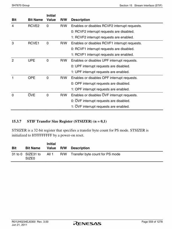
Section 15 Stream Interface (STIF)
R01UH0234EJ0300 Rev. 3.00 Page 559 of 1278 Jun 21, 2011
SH7670 Group
Bit Bit Name Initial Value R/W Description
4 RCVE2 0 R/W Enables or disables RCVF2 interrupt requests.
0: RCVF2 interrupt requests are disabled.
1: RCVF2 interrupt requests are enabled.
3 RCVE1 0 R/W Enables or disables RCVF1 interrupt requests.
0: RCVF1 interrupt requests are disabled.
1: RCVF1 interrupt requests are enabled.
2 UPE 0 R/W Enables or disables UPF interrupt requests.
0: UPF interrupt requests are disabled.
1: UPF interrupt requests are enabled.
1 OPE 0 R/W Enables or disables OPF interrupt requests.
0: OPF interrupt requests are disabled.
1: OPF interrupt requests are enabled.
0 OVE 0 R/W Enables or disables OVF interrupt requests.
0: OVF interrupt requests are disabled.
1: OVF interrupt requests are enabled.
15.3.7 STIF Transfer Size Register (STSIZER) (n = 0,1)
STSIZER is a 32-bit register that specifies a transfer byte count for PS mode. STSIZER is initialized to H'FFFFFFFF by a power-on reset.
Bit Bit Name Initial Value R/W Description
31 to 0 SIZE31 to SIZE0
All 1 R/W Transfer byte count for PS mode

Section 15 Stream Interface (STIF)
Page 560 of 1278 R01UH0234EJ0300 Rev. 3.00 Jun 21, 2011
SH7670 Group
15.3.8 STIFPWM Mode Register (STPWMMR)
STPWMMR is a 32-bit register that selects PWM mode, sets PWM control cycle, reference bit shift amount, and reference clock, enables/disables PID filtering, and sets the PID of a PCR packet to be filtered. STPWMMR is initialized to H'00000000 by a power-on reset.
Bit Bit Name Initial Value R/W Description
31 to 29 ⎯ All 0 R Reserved
These bits are always read as 0. The write value should always be 0.
28 to 16 PID12 to PID0
All 0 R/W These bits set the PID (PCR_PID) of filtering target PCR packet.
15 PIDEN 0 R/W Enables or disables PCR packet filtering.
0: Filtering is disabled.
1: Filtering is enabled.
14 PWMUEN 0 R/W Selects whether to reflect the PWM control difference (internal STC - internal PCR) in the PWM control output according to the comparison of the residual upper bits (comparison target bits) in the comparison of bits 0 to 11. The comparison result of target bits is reflected in UNZF. This bit is valid only when PWMSEL is 0.
0: When the comparison results in a mismatch, PWM control variable is reflected in PWM control.
[Match: UNZF = 0] PWM control variable is reflected in PWM output control.
[Mismatch: UNZF = 1] PWM control variable is reflected in PWM output control.
1: When the comparison results in a mismatch, PWM control variable is not reflected in PWM control.
[Match: UNZF = 0] PWM control variable is reflected in PWM output control.
[Mismatch: UNZF = 1] PWM control variable is not reflected in PWM output control.

Section 15 Stream Interface (STIF)
R01UH0234EJ0300 Rev. 3.00 Page 561 of 1278 Jun 21, 2011
SH7670 Group
Bit Bit Name Initial Value R/W Description
13 PWMSEL 0 R/W Selects difference (internal STC - internal PCR) result or PWMR value for use as the input to selector 2 (figure 15.9).
Also selects PCR arrival pulse or PWMWP as the pulse for reflecting the selector 2 output in the PWM output.
0: PWM control mode is set for the difference (internal STC - internal PCR) result control. PCR arrival pulse and PWMWP are available.
1: PWM control mode is set for the PWMR control.
Only PWMWP is available.
12 PWMSEL2 0 R/W Selects selector 1 (figure 15.9) or addition (selector 1 output + internal PWM) result for use as input to the internal PWM.
0: Selector 1 output is set for input to the internal PWM.
1: Addition (selector 1 output + internal PWM) result is set for input to the internal PWM.
11
10
9
8
PWMCYC3
PWMCYC2
PWMCYC1
PWMCYC0
0
0
0
0
R/W
R/W
R/W
R/W
These bits set a PWM control cycle value based on the PWM reference clock that is set by the PWMDIV bits.
See table 15.2.
This setting should be modified only when the PIDEN bit is 0.
7
6
5
4
PWMSFT3
PWMSFT2
PWMSFT1
PWMSFT0
0
0
0
0
R/W
R/W
R/W
R/W
These bits set a reference bit position that is used to specify the PWM control variable (internal STC - internal PCR). As shown in figure 15.9, the reference bit position of the PWM control variable varies with the PWMSFT value.
This setting should be modified only when the PIDEN bit is 0.
Reference bit position Reference bit position
0000: 0 1000: 8
0001: 1 1001: 9
0010: 2 1010: 10
0011: 3 1011: 11
0100: 4 1100: 12
0101: 5 1101: 13
0110: 6 1110: 14
0111: 7 1111: 15

Section 15 Stream Interface (STIF)
Page 562 of 1278 R01UH0234EJ0300 Rev. 3.00 Jun 21, 2011
SH7670 Group
Bit Bit Name Initial Value R/W Description
3
2
1
0
PWMDIV3
PWMDIV2
PWMDIV1
PWMDIV0
0
0
0
0
R/W
R/W
R/W
R/W
These bits set the reference clock of the PWM control output (PWMOUT) as a system clock (Bφ) division count. Set a division count between 1 and 1024. If a value outside the range is set, the operation of this LSI is not guaranteed.
This setting should be modified only when the PIDEN bit is 0.
0000: 1 1000: 256
0001: 2 1001: 512
0010: 4 1010: 1024
0011: 8 1011: 2048 (invalid)
0100: 16 1100: 4096 (invalid)
0101: 32 1101: 8192 (invalid)
0110: 64 1110: 16384 (invalid)
0111: 128 1111: 32768 (invalid)

Section 15 Stream Interface (STIF)
R01UH0234EJ0300 Rev. 3.00 Page 563 of 1278 Jun 21, 2011
SH7670 Group
Table 15.2 PWM Control Cycle
Bits 11 to 8 Description
PWMCYC3 to PWMCYC0
PWM Cycle (× PWM reference clock)
Acceptable Comparison Bit Count n
Acceptable Comparison (Internal STC - Internal PCR) Result Range *1
PWM Control Variable*2
(ILGL = 1)
0000 2 0 ⎯ ⎯
0001 4 1 –1 to +1 –2
0010 8 2 –3 to +3 –4
0011 16 3 –7 to +7 –8
0100 32 4 –15 to +15 –16
0101 64 5 –31 to +31 –32
0110 128 6 –63 to +63 –64
0111 256 7 –127 to +127 –128
1000 512 8 –255 to +255 –256
1001 1024 9 –511 to +511 –512
1010 2048 10 –1023 to +1023 –1024
1011 4096 11 –2047 to +2047 –2048
1100 8192 12 –4095 to +4095 –4096
1101 16384 13 –8191 to +8191 –8192
1110 32768 14 –16383 to +16383 –16384
1111 65536 15 –32767 to +32767 –32768
Notes: 1. When PWMSEL = 0, if the comparison (internal STC - internal PCR) result exceeds the acceptable comparison result range, the UNZF bit is set to 1.
2. If the PWM control variable is -(2^n), it is treated as an invalid PWM control variable (ILGL = 1) and the UNZF bit is set to 1. The PWM control variable is selected by the PWMSEL bit.

Section 15 Stream Interface (STIF)
Page 564 of 1278 R01UH0234EJ0300 Rev. 3.00 Jun 21, 2011
SH7670 Group
15.3.9 STIFPWM Control Register (STPWMCR)
STPWMCR is a 32-bit register that specifies the generation of write pulses of the internal PCR and STC registers. STPWMCR is initialized to H'00000000 by a power-on reset.
Bit Bit Name Initial Value R/W Description
31 to 9 ⎯ All 0 R Reserved
These bits are always read as 0. The write value should always be 0.
8 STCXP 0 R/W Setting this bit to 1 causes the STC value to be transferred to STSTC0R and STSTC1R.
This bit is automatically cleared to 0.
7 PWMBRS 0 R/W Setting this bit to 1 causes the internal PWM register value to be transferred to STPWM (PWMB).
This bit is automatically cleared to 0.
6 PWMBWP 0 R/W Setting this bit to 1 causes the STPWM (PWMB) value to be reflected in PWM.
PWM control is immediately performed with the value that is set in PWM. Loading with this bit can preferentially be performed independently of the PWMSEL and PWMUEN settings, except when the PWM control variable is an invalid value as described in the UNZF bit field of STSTR. If this bit is set to 1 together with the PWMWP bit, PWMBWP takes precedence.
This bit is automatically cleared to 0.
5 PWMRS 0 R/W Setting this bit to 1 causes the difference (internal STC - internal PCR) result to be transferred to STPWM (PWM).
The difference result is masked by the PWMCYC bits (validity comparison bits) of STPWMMR as shown in figure 15.9.
This bit is automatically cleared to 0.

Section 15 Stream Interface (STIF)
R01UH0234EJ0300 Rev. 3.00 Page 565 of 1278 Jun 21, 2011
SH7670 Group
Bit Bit Name Initial Value R/W Description
4 PWMWP 0 R/W Setting this bit to 1 causes the selector 2 output to be reflected in PWM.
Loading with this bit can be performed preferentially without depending on the PWMSEL and PWMUEN settings, except when the PWM control variable is an invalid value as described in the UNZF bit field of STSTR. If this bit is set to 1 together with the PWMWP bit, PWMBWP takes precedence.
This bit is automatically cleared to 0.
3 STCRS 0 R/W Setting this bit to 1 causes the STC value to be transferred to STSTC0R and STSTC1R.
This bit is automatically cleared to 0.
2 STCWP 0 R/W Setting this bit to 1 causes the STSTC0R and STSTC1R values to be transferred to STC.
If the transfer conflicts with the data write after PCR is received, the transfer using the write pulse of this register takes precedence.
This bit is automatically cleared to 0.
1 PCRRS 0 R/W Setting this bit to 1 causes the PCR value to be transferred to STPCR0R and STPCR1R.
This bit is automatically cleared to 0.
0 PCRWP 0 R/W Setting this bit to 1 causes the STPCR0R and STPCR1R values to be transferred to PCR.
If the transfer conflicts with the data write after PCR is received, the transfer using the write pulse of this register takes precedence.
This bit is automatically cleared to 0.

Section 15 Stream Interface (STIF)
Page 566 of 1278 R01UH0234EJ0300 Rev. 3.00 Jun 21, 2011
SH7670 Group
15.3.10 STIFPWM Register (STPWMR)
STPWMR is a 32-bit register that directly sets PWM control variable. STPWMR is initialized to H'00000000 by a power-on reset.
Bit Bit Name Initial Value R/W Description
31 to 16 PWMB15 to PWMB0
All 0 R/W These bits set a PWM control value equivalent to the comparison (internal STC - internal PCR) result.
To reflect the PWMB value in the PWMOUT output pin as a PWM control variable, set the PWMBWP bit in STPWMCR to 1. Set a PWMB value of two's complement (bit n = sign bit) out of the acceptable comparison bit count n specified by the PWMCYC bits. The acceptable setting range is -(2^n - 1) to +(2^n - 1) where n = acceptable comparison bit count specified by the PWMCYC bits. Do not set the value -(2^n). If -(2^n) is set and is attempted to reflect in the PWM control by setting PWMBWP to 1, it is treated as an invalid PWM control variable setting and the UNZF bit is set to 1. The setting is not reflected in the PWM control output. Note that reflection in the PWM control output is not performed until PWMB is set to a value other than -(2^n).
15 to 0 PWM15 to PWM0
All 0 R/W These bits set a PWM control value equivalent to the comparison (internal STC - internal PCR) result.
To reflect the PWM value in the PWMOUT output pin as a PWM control variable, set the PWMWP bit in STPWMCR to 1 with PWMSEL = 1. Set a PWM value of two's complement (bit n = sign bit) out of the acceptable comparison bit count n specified by the PWMCYC bits. The acceptable setting range is -(2^n - 1) to +(2^n - 1) where n = acceptable comparison bit count specified by the PWMCYC bits. Set a value so that the selector 2 output is not the value -(2^n). When the selector 2 output is -(2^n) and the PWM value is reflected in the PWM control by setting PWMWP to 1, the PWM value is treated as an invalid PWM control variable setting and the UNZF bit is set to 1, The setting is not reflected in the PWM control output.

Section 15 Stream Interface (STIF)
R01UH0234EJ0300 Rev. 3.00 Page 567 of 1278 Jun 21, 2011
SH7670 Group
15.3.11 STIFPCR0, STIFPCR01 Registers (STPCR0R, STPCR1R)
STPCR0R and STPCR1R are 32-bit registers that interface with the internal PCR register. STPCR0R and STPCR1R are initialized to H'00000000 by a power-on reset. These registers compose a 42-bit register including PCR base (33 bits) and PCR extension (9 bits). The PCR base and PCR extension are stored in PCRB32 to PCRB0 and PCRX8 to PCRX0 respectively. Reading or writing this 42-bit register does not cause the read/write result to be reflected directly in clock recovery.
• STPCR0R
Bit Bit Name Initial Value R/W Description
31 to 10 ⎯ All 0 R Reserved
These bits are always read as 0. The write value should always be 0.
9 to 0 PCRB32 to PCRB23
All 0 R/W PCR Base
• STPCR1R
Bit Bit Name Initial Value R/W Description
31 to 9 PCRB22 to PCRB0
All 0 R/W PCR Base
8 to 0 PCRX8 to PCRX0
All 0 R/W PCR Extension
Note: If PCR_PID arrives during data read, the read value is overwritten and becomes undefined. Therefore, confirm that there is no PCR_PID during data read with the PCRF bit in STSTR. Specifically, set the PCRF bit to 0 and then start reading the receive data. Whenever PCRF is 1, take this procedure.
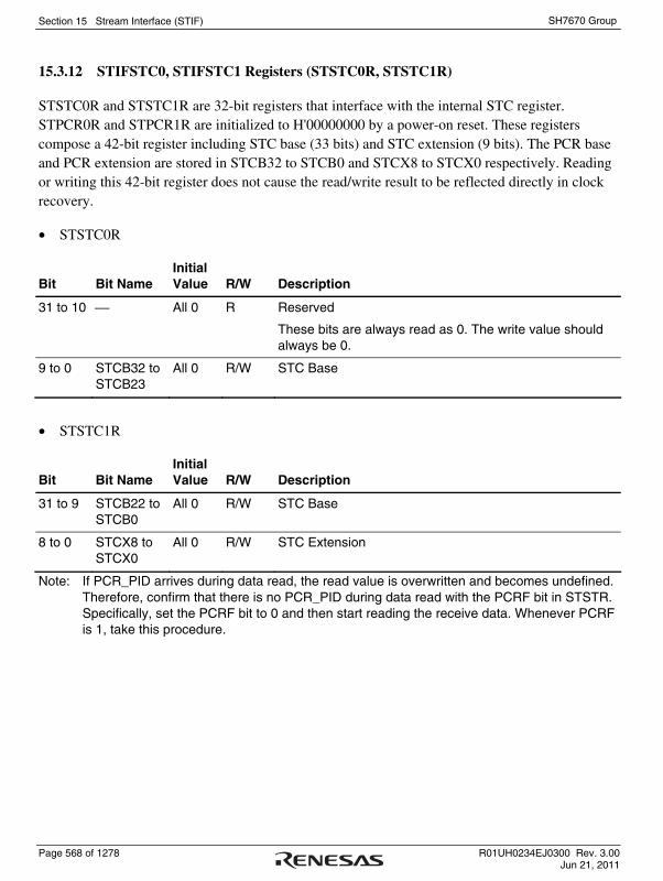
Section 15 Stream Interface (STIF)
Page 568 of 1278 R01UH0234EJ0300 Rev. 3.00 Jun 21, 2011
SH7670 Group
15.3.12 STIFSTC0, STIFSTC1 Registers (STSTC0R, STSTC1R)
STSTC0R and STSTC1R are 32-bit registers that interface with the internal STC register. STPCR0R and STPCR1R are initialized to H'00000000 by a power-on reset. These registers compose a 42-bit register including STC base (33 bits) and STC extension (9 bits). The PCR base and PCR extension are stored in STCB32 to STCB0 and STCX8 to STCX0 respectively. Reading or writing this 42-bit register does not cause the read/write result to be reflected directly in clock recovery.
• STSTC0R
Bit Bit Name Initial Value R/W Description
31 to 10 ⎯ All 0 R Reserved
These bits are always read as 0. The write value should always be 0.
9 to 0 STCB32 to STCB23
All 0 R/W STC Base
• STSTC1R
Bit Bit Name Initial Value R/W Description
31 to 9 STCB22 to STCB0
All 0 R/W STC Base
8 to 0 STCX8 to STCX0
All 0 R/W STC Extension
Note: If PCR_PID arrives during data read, the read value is overwritten and becomes undefined. Therefore, confirm that there is no PCR_PID during data read with the PCRF bit in STSTR. Specifically, set the PCRF bit to 0 and then start reading the receive data. Whenever PCRF is 1, take this procedure.
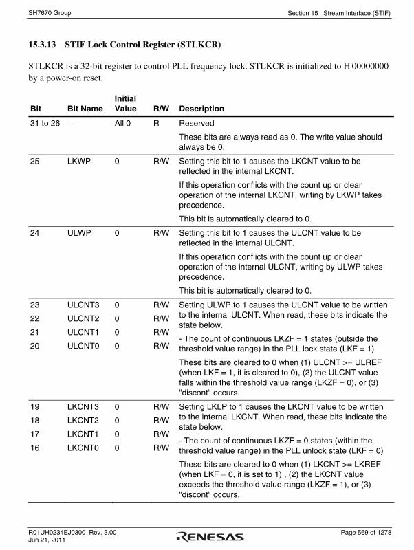
Section 15 Stream Interface (STIF)
R01UH0234EJ0300 Rev. 3.00 Page 569 of 1278 Jun 21, 2011
SH7670 Group
15.3.13 STIF Lock Control Register (STLKCR)
STLKCR is a 32-bit register to control PLL frequency lock. STLKCR is initialized to H'00000000 by a power-on reset.
Bit Bit Name Initial Value R/W Description
31 to 26 ⎯ All 0 R Reserved
These bits are always read as 0. The write value should always be 0.
25 LKWP 0 R/W Setting this bit to 1 causes the LKCNT value to be reflected in the internal LKCNT.
If this operation conflicts with the count up or clear operation of the internal LKCNT, writing by LKWP takes precedence.
This bit is automatically cleared to 0.
24 ULWP 0 R/W Setting this bit to 1 causes the ULCNT value to be reflected in the internal ULCNT.
If this operation conflicts with the count up or clear operation of the internal ULCNT, writing by ULWP takes precedence.
This bit is automatically cleared to 0.
23
22
21
20
ULCNT3
ULCNT2
ULCNT1
ULCNT0
0
0
0
0
R/W
R/W
R/W
R/W
Setting ULWP to 1 causes the ULCNT value to be written to the internal ULCNT. When read, these bits indicate the state below.
- The count of continuous LKZF = 1 states (outside the threshold value range) in the PLL lock state (LKF = 1)
These bits are cleared to 0 when (1) ULCNT >= ULREF (when LKF = 1, it is cleared to 0), (2) the ULCNT value falls within the threshold value range (LKZF = 0), or (3) "discont" occurs.
19
18
17
16
LKCNT3
LKCNT2
LKCNT1
LKCNT0
0
0
0
0
R/W
R/W
R/W
R/W
Setting LKLP to 1 causes the LKCNT value to be written to the internal LKCNT. When read, these bits indicate the state below.
- The count of continuous LKZF = 0 states (within the threshold value range) in the PLL unlock state (LKF = 0)
These bits are cleared to 0 when (1) LKCNT >= LKREF (when LKF = 0, it is set to 1) , (2) the LKCNT value exceeds the threshold value range (LKZF = 1), or (3) "discont" occurs.

Section 15 Stream Interface (STIF)
Page 570 of 1278 R01UH0234EJ0300 Rev. 3.00 Jun 21, 2011
SH7670 Group
Bit Bit Name Initial Value R/W Description
15
14
13
12
GAIN3
GAIN2
GAIN1
GAIN0
0
0
0
0
R/W
R/W
R/W
R/W
These bits are used to control the right-shift amount that gains the error amount to be input to the adder from selector 1. Since the error amount is expressed as a two's complement, an arithmetic shift is used for right shift. That is, the most significant sign bit is copied to the bits that become short by the right shift for refill. Select a value between 0 and 10 for the right-shift amount of error amount. If a value outside the range is set, the setting is invalid and the operation is not guaranteed.
Right-shift amount Right-shift amount
0000: 0 1000: 8
0001: 1 1001: 9
0010: 2 1010: 10
0011: 3 1011: 11 (invalid)
0100: 4 1100: 12 (invalid)
0101: 5 1101: 13 (invalid)
0110: 6 1110: 14 (invalid)
0111: 7 1111: 15 (invalid)
11
10
9
8
LKCYC3
LKCYC2
LKCYC1
LKCYC0
0
0
0
0
R/W
R/W
R/W
R/W
These bits set a PLL lock threshold value. For PLL lock threshold values, see table 15.3. Set an LKCYC value that is not larger than PWMCYC (LKCYC =< PWMCYC). If a value larger than PWMCYC is set, the operation is not guaranteed.
7
6
5
4
ULREF3
ULREF2
ULREF1
ULREF0
0
0
0
0
R/W
R/W
R/W
R/W
These bits specify a reference value for the number of continuous LKZF = 1 states (outside the threshold value range) when PLL is locked (LKF = 1). This value is compared with the ULCNT value. When ULCNT >= ULREF, the LKF bit in STSTR is set to 0.
3
2
1
0
LKREF3
LKREF2
LKREF1
LKREF0
0
0
0
0
R/W
R/W
R/W
R/W
These bits specify a reference value for the number of continuous LKZF = 0 states (within the threshold value range) when PLL is unlocked (LKF = 0). This value is compared with the LKCNT value. When LKCNT >= LKREF, the LKF bit in STSTR is set to 1.

Section 15 Stream Interface (STIF)
R01UH0234EJ0300 Rev. 3.00 Page 571 of 1278 Jun 21, 2011
SH7670 Group
Table 15.3 PLL Lock Threshold Value
Bits 11 to 8 Description
LKCYC3 to LKCYC0
PLL Lock Threshold Value (× PWM Reference Clock)
Acceptable Comparison Bit Count n
Acceptable Comparison (Internal STC - Internal PCR) Result Range *1
PWM Control Variable*2
(ILGL = 1)
0000 2 0 ⎯ ⎯
0001 4 1 –1 to +1 –2
0010 8 2 –3 to +3 –4
0011 16 3 –7 to +7 –8
0100 32 4 –15 to +15 –16
0101 64 5 –31 to +31 –32
0110 128 6 –63 to +63 –64
0111 256 7 –127 to +127 –128
1000 512 8 –255 to +255 –256
1001 1024 9 –511 to +511 –512
1010 2048 10 –1023 to +1023 –1024
1011 4096 11 –2047 to +2047 –2048
1100 8192 12 –4095 to +4095 –4096
1101 16384 13 –8191 to +8191 –8192
1110 32768 14 –16383 to +16383 –16384
1111 65536 15 –32767 to +32767 –32768
Notes: 1. When the comparison (internal STC - internal PCR) result falls within the acceptable comparison result range, the LKZF bit is set to 0.
2. If the PWM control variable is -(2^n), it is treated as an invalid PWM control variable (ILGL = 1) and the LKZF bit is set to 1. The PWM control variable is selected by the PWMSEL and PWMSEL2 bits.

Section 15 Stream Interface (STIF)
Page 572 of 1278 R01UH0234EJ0300 Rev. 3.00 Jun 21, 2011
SH7670 Group
15.3.14 STIF Debugging Status Register (STDBGR)
STDBGR is a 32-bit register that indicates the first four bytes of an input or output packet. STDBGR is provided for debugging. The write value should always be 0.
Bit Bit Name Initial Value R/W Description
31 to 0 STMON31 to STMON0
All 0 R The 4-byte timestamp of a packet that is input or output in TS mode is stored.
This means that when the STIF receives a TS packet (188 bytes) from an external device, the 4-byte timestamp that will be added to the beginning of the TS packet by the STIF is stored. When the STIF outputs a TS packet to an external device, the 4-byte timestamp that was added to the beginning of the TTS packet (192 bytes) is stored.
This register cannot be used in TTS mode or PS mode.
15.4 Examples of Clock Connection to Another Device
Examples of clock connection to another device are illustrated below.
15.4.1 A Basic Example
Another device This LSI
CLKOUT (output)
CLKIN (input)
SYC (input/output)
VLD (input/output)
D[7:0] (input/output)
ST0_CLKIN (input)
ST_CLKOUT (output)
STn_SYC (input/output)
STn_VLD (input/output)
STn_D[7:0] (input/output)
(n = 0, 1)
• When this LSI receives a stream, it is received in synchronization with STn_CLKIN.
• When this LSI sends a stream, it is sent in synchronization with ST_CLKOUT.

Section 15 Stream Interface (STIF)
R01UH0234EJ0300 Rev. 3.00 Page 573 of 1278 Jun 21, 2011
SH7670 Group
15.4.2 An Example of Clock Connection When Another Device Has No Clock Input
Another device This LSI
CLKOUT (output)
SYC (input/output)
VLD (input/output)
D[7:0] (input/output)
ST0_CLKIN (input)
ST_CLKOUT (output)
STn_SYC (input/output)
STn_VLD (input/output)
STn_D[7:0] (input/output)
open
(n = 0, 1)
• When this LSI receives a stream, it is received in synchronization with STn_CLKIN.
• When this LSI sends a stream, it is sent in synchronization with STn_CLKIN.
15.4.3 An Example of Clock Connection When Another Device Has No Clock Output
Another device This LSI
CLKIN (input)
SYC (input/output)
VLD (input/output)
D[7:0] (input/output)
STn_CLKIN (input)
ST_CLKOUT (output)
STn_SYC (input/output)
STn_VLD (input/output)
STn_D[7:0] (input/output)
(n = 0, 1)
• When this LSI receives a stream, it is received in synchronization with STn_CLKIN.
• When this LSI sends a stream, it is sent in synchronization with ST_CLKOUT.
15.5 Input/Output Timing
Figures 15.2 to 15.7 show the operation overview and input/output timing of each mode.

Section 15 Stream Interface (STIF)
Page 574 of 1278 R01UH0234EJ0300 Rev. 3.00 Jun 21, 2011
SH7670 Group
SHSTIF
+4 byteTimestamp added
192 byte
SHLocal bus
188 byte
PUSH control systemSYC, VLD, D
SHSTIF-4 byteTimestamp removedOutput control accordingto timestamp
192 byte
SHLocal bus
188 byte
REQ
PUSH control systemSYC, VLD, D
Schematic diagram of TS mode 1 and TS mode 2
SHSTIF
+4 byteTimestamp added
192 byte
SHLocal bus
188 byte
PULL control systemSYC, VLD, D
SHSTIF-4 byteTimestamp removal onlyData output control accordingto REQ input
192 byte
SHLocal bus
188 byte
PULL control systemSYC, VLD, D
Schematic diagram of TS mode 3
SHSTIFFile transfer imageNo timestamp is addedor removed.192 bytes fixed
192 byte
SHLocal bus
192 byte
PULL control systemVLD, D
SHSTIFFile transfer imageNo timestamp is addedor removed.192 bytes fixedData output control accordingto REQ input
192 byte
SHLocal bus
192 byte
PULL control systemVLD, D
Schematic diagram of TTS mode
SHSTIFFile transfer imageNo timestamp is addedor removed.Transfer size is determinedby size register.
File transfer imageNo timestamp is addedor removed.Transfer size is determinedby size register.Data output control accordingto REQ input
n byte(n: Integer)
SHLocal bus
n byte (n: Integer)
PULL control systemVLD, D
SHSTIF n byte
(n: Integer)
SHLocal bus
n byte (n: Integer)
PULL control systemVLD, D
Schematic diagram of PS mode
REQ
REQ
REQ
REQ
REQ
Figure 15.2 Operation Overview
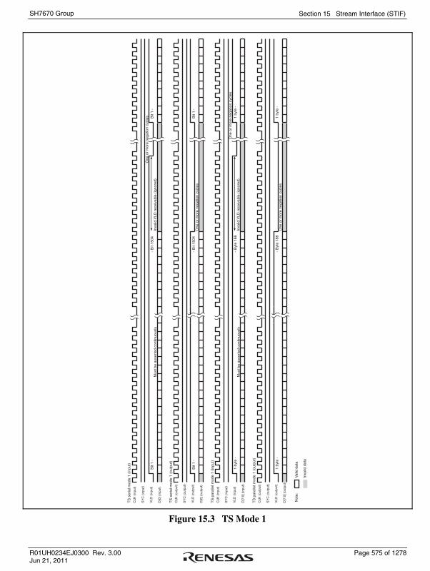
Section 15 Stream Interface (STIF)
R01UH0234EJ0300 Rev. 3.00 Page 575 of 1278 Jun 21, 2011
SH7670 Group
CLK
(in
put)
TS
ser
ial m
ode
1 (in
put)
SY
C (
inpu
t)
VLD
(in
put)
D[0
] (in
put)
Bit
1 -
Bit
1 -
- B
it 15
04In
valid
VLD
rec
eiva
ble
(igno
red)
Inva
lid V
LD r
ecei
vabl
e (ig
nore
d)
Mus
t be
asse
rted
con
tinuo
usly
One
or
mor
e ne
gatio
n cy
cles
CLK
(ou
tput
)
TS
ser
ial m
ode
1 (o
utpu
t)
SY
C (
outp
ut)
VLD
(ou
tput
)
D[0
] (ou
tput
)
Bit
1 -
Bit
1 -
- B
it 15
04O
ne o
r m
ore
nega
tion
cycl
es
CLK
(in
put)
TS
par
alle
l mod
e 1
(inpu
t)
SY
C (
inpu
t)
VLD
(in
put)
D[7
:0] (
inpu
t)
1 by
te -
1 by
te -
- B
yte
188
Mus
t be
asse
rted
con
tinuo
usly
One
or
mor
e ne
gatio
n cy
cles
CLK
(ou
tput
)
TS
par
alle
l mod
e 1
(out
put)
SY
C (
outp
ut)
VLD
(ou
tput
)
D[7
:0] (
outp
ut)
1 by
te -
1 by
te -
- B
yte
188
One
or
mor
e ne
gatio
n cy
cles
Not
e:V
alid
dat
a
Inva
lid d
ata
Figure 15.3 TS Mode 1

Section 15 Stream Interface (STIF)
Page 576 of 1278 R01UH0234EJ0300 Rev. 3.00 Jun 21, 2011
SH7670 Group
Bit
1 -
Bit
1 -
- B
it 15
04
CLK
(in
put)
TS
ser
ial m
ode
2 (in
put)
SY
C (
inpu
t)
VLD
(in
put)
D[0
] (in
put)
Bit
1 -
-B
it 1
--
Bit
1504
Can
be
cont
inuo
us o
r se
para
te.
Inva
lid V
LD r
ecei
vabl
e (ig
nore
d)C
an b
e co
ntin
uous
or
sepa
rate
.
One
-cyc
le a
sser
tion
and
cont
inuo
us a
sser
tion
(unt
il 18
8-by
te tr
ansf
er e
nd) a
re b
oth
acce
ptab
le.
CLK
(ou
tput
)
TS
ser
ial m
ode
2 (o
utpu
t)
SY
C (
outp
ut)
VLD
(ou
tput
)
D[0
] (ou
tput
)
CLK
(in
put)
TS
par
alle
l mod
e 2
(inpu
t)
SY
C (
inpu
t)
VLD
(in
put)
D[7
:0] (
inpu
t)
CLK
(ou
tput
)
TS
par
alle
l mod
e 2
(out
put)
SY
C (
outp
ut)
VLD
(ou
tput
)
D[7
:0] (
outp
ut)
Not
e:V
alid
dat
a
Inva
lid d
ata
One
or
mor
e ne
gatio
n cy
cles
Ass
erte
d fo
r 8
bits
1 by
te -
1 by
te -
- B
yte
188
1 by
te -
-1
byte
--
Byt
e 18
8C
an b
e co
ntin
uous
or
sepa
rate
.In
valid
VLD
rec
eiva
ble
(igno
red)
Can
be
cont
inuo
us o
r se
para
te.
One
-cyc
le a
sser
tion
and
cont
inuo
us a
sser
tion
(unt
il 18
8-by
te tr
ansf
er e
nd) a
re b
oth
acce
ptab
le.
One
or
mor
e ne
gatio
n cy
cles
SY
C m
ust b
e ne
gate
d fo
r at
leas
t one
cyc
le.
VLD
mus
t be
nega
ted
for
at le
ast o
ne c
ycle
.
VLD
mus
t be
nega
ted
for
at le
ast o
ne c
ycle
.
SY
C m
ust b
e ne
gate
d fo
r at
leas
t one
cyc
le.
Figure 15.4 TS Mode 2

Section 15 Stream Interface (STIF)
R01UH0234EJ0300 Rev. 3.00 Page 577 of 1278 Jun 21, 2011
SH7670 Group
Can
be
cont
inuo
us o
r se
para
te.
CLK
(in
put)
TS
ser
ial m
ode
3 (in
put)
RE
Q (
outp
ut)
SY
C (
inpu
t)
VLD
(in
put)
D[0
] (in
put)
CLK
(ou
tput
)
TS
ser
ial m
ode
3 (o
utpu
t)
RE
Q (
inpu
t)
SY
C (
outp
ut)
VLD
(ou
tput
)
D[0
] (ou
tput
)
Not
e:V
alid
dat
a
Inva
lid d
ata
Bit
1 -
No
rest
rictio
n fo
r in
put l
aten
cy
Bit
1 -
- B
it 15
04
Bit
1 -
Bit
1 -
- B
it 15
04
min
1cy
c
Can
be
cont
inuo
us o
r se
para
te.
CLK
(in
put)
TS
par
alle
l mod
e 3
(inpu
t)
RE
Q (
outp
ut)
SY
C (
inpu
t)
VLD
(in
put)
D[7
:0] (
inpu
t)
1 by
te -
No
rest
rictio
n fo
r in
put l
aten
cy
1 by
te -
- B
yte
188
CLK
(ou
tput
)
TS
par
alle
l mod
e 3
(out
put)
RE
Q (
inpu
t)
SY
C (
outp
ut)
VLD
(ou
tput
)
D[7
:0] (
outp
ut)
1 by
te -
1 by
te -
- B
yte
188
min
1cy
c
Min
imum
2-c
lock
late
ncy
from
VLD
inpu
t neg
atio
n (b
it 15
04)
until
RE
Q o
utpu
t neg
atio
n
Min
imum
1-c
lock
late
ncy
from
VLD
inpu
t neg
atio
n (b
yte
188)
unt
il R
EQ
out
put n
egat
ion
Up
to 1
-bit
over
run
from
RE
Q in
put n
egat
ion
until
VLD
out
put n
egat
ion
Up
to 1
-bit
over
run
from
RE
Q in
put n
egat
ion
until
VLD
out
put n
egat
ion
Figure 15.5 TS Mode 3
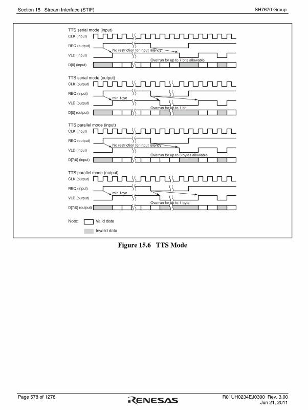
Section 15 Stream Interface (STIF)
Page 578 of 1278 R01UH0234EJ0300 Rev. 3.00 Jun 21, 2011
SH7670 Group
CLK (input)
TTS serial mode (input)
REQ (output)
VLD (input)
D[0] (input)
No restriction for input latency
Overrun for up to 7 bits allowable
Note: Valid data
Invalid data
CLK (output)
TTS serial mode (output)
REQ (input)
VLD (output)
D[0] (output)
min 1cyc
Overrun for up to 1 bit
CLK (input)
TTS parallel mode (input)
REQ (output)
VLD (input)
D[7:0] (input)
No restriction for input latency
Overrun for up to 3 bytes allowable
CLK (output)
TTS parallel mode (output)
REQ (input)
VLD (output)
D[7:0] (output)
min 1cyc
Overrun for up to 1 byte
Figure 15.6 TTS Mode

Section 15 Stream Interface (STIF)
R01UH0234EJ0300 Rev. 3.00 Page 579 of 1278 Jun 21, 2011
SH7670 Group
CLK (input)
PS serial mode (input)
REQ (output)
VLD (input)
D[0] (input)
No restriction for input latency
Overrun for up to 7 bits allowable
Note: Valid data
Invalid data
CLK (output)
PS serial mode (output)
REQ (input)
VLD (output)
D[0] (output)
min 1cyc
Overrun for up to 1 bit
CLK (input)
PS parallel mode (input)
REQ (output)
VLD (input)
D[7:0] (input)
No restriction for input latency
Overrun for up to 3 bytes allowable
CLK (output)
PS parallel mode (output)
REQ (input)
VLD (output)
D[7:0] (output)
min 1cyc
Overrun for up to 1 byte
Figure 15.7 PS Mode

Section 15 Stream Interface (STIF)
Page 580 of 1278 R01UH0234EJ0300 Rev. 3.00 Jun 21, 2011
SH7670 Group
15.6 PCR Clock Recovery Module (PCRRCV)
The PCR clock recovery module (PCRRCV) is a circuit to provide a PWM (pulse wave modulation) output for controlling the external VCXO circuit according to the difference between 42-bit program_clock_reference (PCR) and system reference clock (STC). The PCR consists of program_colck_reference_base (PCR base) and program_clock_reference_extension (PCR extension) of adaptation_field in an input transport (TS) packet.
The PCRRCV has the following features.
• A 42-bit internal STC counter triggered by the clock input from the external VCXO circuit
• PWM output for controlling the external VCXO circuit can be output on the STn_PWMOUT pin.
• VCXO control is selectable from PWM control mode according to the difference between PCR and STC in a TS packet or PWM control mode by directly setting STPWMR.
• PWM control accuracy and PWM cycle can be set in STPWMMR.
PCRRCV
[Legend]VCXO:LPF:PWMOUT:VOXO (27MHz):
VCXO clock input pinLow Pass FilterPWM control output pinVoltage control oscillator
VOXO(27MHz)
VCXO
LPF
PWMOUT
Figure 15.8 STn_VCO_CLKIN and STn_PWMOUT Connections

Section 15 Stream Interface (STIF)
R01UH0234EJ0300 Rev. 3.00 Page 581 of 1278 Jun 21, 2011
SH7670 Group
15.6.1 Operation of PCR Clock Recovery
Internal PCR
Internal PCR and STC values are binary-converted,and then the difference between them is calculated.
(32 bits)PCR base
(16 bits)
Selector 1
Selector 2
(16 bits)
(9 bits)PCR ext
PWMCYC+1
PWMCYC+1
PWMCYC+1PWMCYC+1
Cycle: PWMCYC × PWMDIV
PWMOUT high PWMOUT low
PWMCYC+1
PWMSFT
PWMSEL
PWMSEL2
GAIN
Internal STC
STC value -PCR value
Internal PWM
Right shift
LKZF
UNZF
PWMR
PWMBR
Upper-sidecomparison target
Upper-sidecomparison target
Sign bit n is refilled by right-shift.(n: Acceptable comparison bitcount specified by PWMCYC)
PWMOUT high = (Inverse value of PWM control variable (except MSB) + 1) × PWMDIVPWMOUT low = (PWMCYC - PWMOUT high) × PWMDIV
PWMOUT outputwaveform
LKCYC+1
(16 bits) (16 bits)
Figure 15.9 Illustration of Register Settings

Section 15 Stream Interface (STIF)
Page 582 of 1278 R01UH0234EJ0300 Rev. 3.00 Jun 21, 2011
SH7670 Group
• Register Settings
A. Specify the acceptable comparison bit count n of the PWM control variable using the PWMCYC3 to PWMCYC0 bits in STPWMMR.
B. Set a PLL lock threshold value using the LKCYC3 to LKCYC0 bits in STLKCR.
C. Specify the shift amount of the PWM control variable reference bit (LSB of PWM control variable) using the PWMSFT3 to PWMSFT0 bits in STPWMMR. The shifted bits (PWMSFT width bits in figure 15.9) do not fall within the PWM control variable comparison range.
D. In the PWM control variable calculation, the PCR base and PCR extension of the internal STC and PCR registers are converted to binary values, and the converted values are masked with the PWMSFT width bits, and then the difference between the values is calculated. The binary conversion is performed using the following expression (1).
Internal STC/PCR binary conversion: (PCR_base × 300 + PCR_ext) & (PWMSFT width mask) …(1)
The upper comparison result except (PWMCYC + 1) of the difference result is reflected in the UNZF bit in STSTR.
The upper comparison result except (LKCYC + 1) of the difference result is reflected in the LKZF bit in STSTR.
E. Specify the right-shift amount of selector 1 output using the GAIN3 to GAIN0 bits in STLKCR. Since an arithmetic shift is used for the right shift, the overflowing bits are discarded on the lower side and the sign bit (bit n when the acceptable comparison bit count = n) is refilled on the upper side.
F. Switch selector 1 and selector 2 using the PWMSEL and PWMSEL2 bits in STPWMMR to select the path to the internal PWM register.
G. Specify the PWM reference clock of the PWMOUT pin using the PWMDIV3 to PWMDIV0 bits in STPWMMR. The PWM reference clock has a cycle of system clock × PWMDIV. The PWM cycle of the PWMOUT pin has a clock cycle of PWMCYC × PWMDIV.
H. The PWMOUT output waveform that depends on the PWM control variable is as follows:
PWMOUT high = (Inverse value of PWM control variable (except MSB) + 1) × PWMDIV …(2a)
PWMOUT low = (PWMCYC - PWMOUT low) × PWMDIV …(2b)
When the acceptable comparison bit count is n, the MSB becomes bit n of the PWM control variable.
The PWM control variable is expressed as a two's complement. Whether to include the upper comparison target in the PWM control range is specified by the PWMUEN bit in STPWMMR.

Section 15 Stream Interface (STIF)
R01UH0234EJ0300 Rev. 3.00 Page 583 of 1278 Jun 21, 2011
SH7670 Group
I. The PWM control variable can directly be set by STPWMR when the PWMSEL bit in STPWMMR is set to 1. In this case, PWMCYC acts as a number of acceptable comparison bits as in the case of internal STC value - PCR value (figure 15.9).
15.6.2 PCR Clock Recovery Operation
PCRRCV
PCR_PID setting
TS packet arrival timeto internal PCR bus
Packet including PCR_PID(packet with PID set by PCR_PID)
Input to PCRRCV upon arrival of PCR
... ...
PCR0 PCR1 PCR2
Figure 15.10 Overview of TS Packet
• Example 1: Clock recovery using the PCRRCV hardware
A. Set PWMSEL to 0 to enable the clock recovery using the PCRRCV hardware.
B. Set the PWMCYC, PWMSFT, PWMDIV, and PWMUEN bits in STPWMMR for the PWM control output.
C. Set the PID bits in STPWMMR to PCR_PID of a packet including PCR for recovering clock to the PCRRCV. The clock recovery starts upon the PID setting. For this reason, if the PCR continuity is impaired by a reset or channel change, set PIDEN to 0 and then set a PID.
D. When a packet including PCR_PID arrives, the PCRRCV extracts the 42-bit program_clock_reference (PCR) from the adaptation_field of the packet. For packet conditions for extracting PCR, see table 15.4. When a TS packet that satisfies the conditions in table 15.4 arrives, a PCR arrival pulse is generated in the PCRRCV.
E. When a PCR arrival pulse is generated, the PCR extracted from the packet is transferred to the internal PCR register and STC counter. The STC counter (STC) value is also transferred to the internal STC register at the same time. After that, the STC counter starts counting by the VCXO clock input. The STC counter value incremented from the previous PCR until the present time by the VCXO clock is set in the internal STC register, and the currently arrived PCR is set in the internal PCR register and STC counter.
F. The PWM control variable, which is the comparison result between the internal STC and PCR registers (STC value - PCR value), is calculated by the PWMCYC, PWMSFT, and PWMDIV bits in STPWMMR. When the comparison result reflection conditions in table 15.5 are satisfied, the comparison result is reflected in the PWM output control. Setting

Section 15 Stream Interface (STIF)
Page 584 of 1278 R01UH0234EJ0300 Rev. 3.00 Jun 21, 2011
SH7670 Group
PWMUEN to 1 disables the PWM control variable outside the acceptable comparison result range specified by the PWMCYC bits to be reflected in the PWM control output. This function can prevent an abnormal PCR (caused by PCR error due to transmission error or protocol violation at the transmitter side) from being reflected in clock recovery. For measures against abnormal PCRs, see the procedure examples 1 and 2 described later.
G. The PWMOUT waveform with a reflected PWM control variable is output from the PWMOUT pin as shown in figure 15.9.
H. The internal STC and PCR register values are compared each time a PCR_PID packet arrives. By configuring a feedback circuit including an external low-pass filter (LPF) and an external VCXO, which makes the comparison (STC value - PCR value) result to be 0, the VCXO clock frequency is adjusted.
• Example 2: Clock recovery using the PCRRCV and software
A. Set PWMSEL to 1 to disable the clock recovery using the PCRRCV hardware. Also set PCRE to 1 to enable interrupt requests made by each PCR arrival pulse.
B. The PCRRCV settings and transfers of the PCRRCV internal registers are the same as those described in steps 2 to 5 of Example 1. Notes 1 to 4 for table 15.5 apply to the case of the first arrival of PCR after the PCR continuity is lost. Since the STC counter that has no continuity with the arrived internal PCR register is transferred to the internal STC register, it is not appropriate to calculate the difference (STC value - PCR value) by the CPU.
C. Confirm that transfer between the PCRRCV internal registers has been completed (PCRF = 1), and then set PCRF to 0. After that, set the STCRS and PCRRS bits to 1 to enable transfer from the STC register to STSTC0R and STSTC1R, as well as transfer from the PCR register to STSTC0R and STSTC1R. Then read STSTC0R/STSTC1R and STPCR0R/STPCR1R. Furthermore, to obtain the STC counter value for setting to the MPEG2 decoder, set the STCXP bit to 1 to enable transfer from the STC counter to STSTC0R and STSTC1R. Then read STSTC0R and STSTC1R.
D. A PCRF read value of 0 means that no PCR_PID packet arrived during the register read stage in step 3. This shows that the reading of STSTC0R/STSTC1R and STPCR0R/STPCR1R in step 3 was successful. On the other hand, a PCRF read value of 1 shows an arrival of PCR_PID packet during the register read stage in step 3. It is not certain that the read STSTC0R/STSTC1R and STPCR0R/STPCR1R are the values of the internal STC and PCR registers that arrived previously or those that arrived during the register read stage. Therefore, go back to step 3 and repeat the procedure.
Section 15 Stream Interface (STIF)
R01UH0234EJ0300 Rev. 3.00 Page 585 of 1278 Jun 21, 2011
SH7670 Group
E. The CPU converts the read STSTC0R/STSTC1R and STPCR0R/STPCR1R values to binary ones with STCbin and PCRbin respectively using the expression (1) in section 15.6.1, Operation of PCR Clock Recovery, step 4, and then calculates the difference (STCbin - PCRbin). To be set in STPWMR as a PWM control variable, specify the difference (STCbin - PCRbin) as a two's complement of the acceptable comparison bit count n (n: sign bit) specified by the PWMCYC bits. Set a value within the range of -(2^n - 1) to +(2^n - 1) for the difference. Do not set the value -2^n. The CPU also determines the handling of PCR data errors shown in step 6 of Example 1.
F. The PWM control variable that is set in STPWMR can be reflected in the PWM control output by writing 1 to PWMWP.
G. For the principle of VCXO clock frequency adjustment using the PWM control output, the descriptions in steps 7 and 8 of Example 1 apply.
Table 15.4 PCR Extraction Conditions
transport_error_ indicator
adaptation_field_control adaptation_field_length PCR_flag PCR Extraction*
00 don't care don't care Impossible
01 don't care don't care Impossible
0 ≤ len < 7 don't care Impossible
0 Impossible
10
7 ≤ len < H'FF
1 Possible
0 ≤ len < 7 don't care Impossible
0 Impossible
0
11
7 ≤ len < H'FF
1 Possible
1 don't care don't care don't care Impossible
Note: * When PCR extraction is possible, PCR is extracted and a PCR arrival pulse is generated.

Section 15 Stream Interface (STIF)
Page 586 of 1278 R01UH0234EJ0300 Rev. 3.00 Jun 21, 2011
SH7670 Group
Table 15.5 Internal PCR and STC Registers Comparison Result Reflection Conditions *1
Reflection Comparison Result Reflection Conditions
Not reflected*2 Arrival of PCR_PID after "discont" *3
Arrival of PCR_PID whose upper comparison result does not match when PWMUEN = 1
Reflected Arrival of PCR_PID in other cases
Notes: 1. When PWMSEL = 0, the reflection conditions in this table are effective. When PWMSEL = 1, the PWM control variable can be reflected in the PWM control output by writing 1 to the PWMWP bit.
2. Since the PWM control variable is not reflected, the PWMOUT waveform is maintained.
3. There are four patterns of PCR_PID arrival after "discont." (1) The first PCR_PID arrival after reset cancellation (2) The first PCR_PID arrival after PCR flush cancellation (3) When discontinuity_indicator of the arrived PCR_PID packet = 1 (4) Arrival of PCR_PID after the PID bits in STPWMMR was modified *4
4. Set PIDEN to 0 before modifying the PID bits in STPWMMR. With this setting, arrival of PCR_PID is treated as arrival after "discont."
• Hardware measures against arrival of abnormal PCRs
Initial setting (1) Set an LKCYC value not larger than the PWMCYC value. The LKCYC value must be larger than the steady-state deviation (error amount) of the PLL that is configured with an external circuit. Determine the LKCYC value with a margin from the PLL's steady-state deviation. Otherwise, the operation of this LSI is not guaranteed.
Initial setting (2) Set an LKREF value until the LKF bit is set to 1 when the PLL error amount falls within the threshold value range. The LKREF bits, which are usually set to 1, are provided for setting to enhance the stability against arrival of abnormal PCRs in the PLL pull-in state. Note that the larger the LKREF value becomes, the higher stability is obtained, but the PLL pull-in time becomes longer.
Initial setting (3) Set a ULREF value until the LKF bit is set to 0 when the PLL error amount exceeds the threshold value limit. The ULREF bits, which are usually set to 1, are provided for setting to enhance the stability against arrival of abnormal PCRs in the PLL lock state. It is recommended that the LKREF value be larger than the maximum of the number of continuous arrivals of system-dependent abnormal PCRs.
Section 15 Stream Interface (STIF)
R01UH0234EJ0300 Rev. 3.00 Page 587 of 1278 Jun 21, 2011
SH7670 Group
15.7 Usage Notes
1. When at least one channel is set to transmit mode (stream output from the SHA to an external device) with the input clock to the ST_CLKIN pin of the relevant channel selected as the transmit clock (CLKSEL bit in STMDR of relevant channel is 1), the ST_CLKOUT pin should be fixed to low-level output (CKFRSEL[3:0] bits in STMDR_0 are 1111).
2. The ST_CLKOUT pin is a common resource for STIF channels. Since it is incorporated in channel 0, the ST_CLKOUT operation is not affected by channel 1 being in module standby mode. When the STIF is in module standby mode, the main clock supplies (Pφ and Bφ) to the relevant channel are stopped. Therefore, if channel 0 enters module standby mode, the ST_CLKOUT operation conforms to the setting of bits CKFRSEL[3:0] in STMDR_0 as shown below.
0000: Output is fixed to low
0001: Iφ/2 (not affected by module standby mode)
0010: Iφ/3 (not affected by module standby mode)
0011: Iφ/4 (not affected by module standby mode)
0100: Iφ/6 (not affected by module standby mode)
0101: Iφ/8 (not affected by module standby mode)
0110: Iφ/12 (not affected by module standby mode)
0111: Reserved (setting prohibited)
1000: Reserved (setting prohibited)
1001: Reserved (setting prohibited)
1010: Reserved (setting prohibited)
1011: Reserved (setting prohibited)
1100: Reserved (setting prohibited)
1101: Reserved (setting prohibited)
1110: Reserved (setting prohibited)
1111: Output is fixed to low
For details on module standby mode, refer to section 11, Power-Down Modes.

Section 15 Stream Interface (STIF)
Page 588 of 1278 R01UH0234EJ0300 Rev. 3.00 Jun 21, 2011
SH7670 Group
3. When a stream from an external device to the STIF is being transferred to memory via the A-DMAC, perform the following processing in the order shown below to pause and resume transfer.
To pause transfer:
(1) Clear the C[i]C_E bit in the channel [i] processing control register (C[i]C) to 0.
(2) Poll the interrupt request flag or wait for an interrupt until the C[i]I_DI bit in the channel [i] processing interrupt request register (C[i]I) becomes 1.
To resume transfer:
(3) Set the C[i]C_E bit in the channel [i] processing control register (C[i]C) to 1.
4. When a stream from memory to the A-DMAC is being transferred to an external device via the STIF, perform the following processing in the order shown below to pause and resume transfer.
To pause transfer:
(1) Clear the C[i]C_E bit in the channel [i] processing control register (C[i]C) to 0.
(2) Poll the interrupt request flag or wait for an interrupt until the C[i]I_DI bit in the channel [i] processing interrupt request register (C[i]I) becomes 1.
To resume transfer:
(3) Set the C[i]C_E bit in the channel [i] processing control register (C[i]C) to 1.
5. When a stream from an external device to the STIF is being transferred to memory via the A-DMAC, perform the following processing in the order shown below to forcibly terminate and resume transfer.
To forcibly terminate transfer:
(1) Clear both the REQEN and EN bits in the STIF control register (STCTLR) to 0.
(2) Clear the C[i]C_E bit to 0 and set the C[i]C_R bit to 1 in the channel [i] processing control register (C[i]C).
(3) Prepare a dummy descriptor. (Specify data transfer from the relevant STIF channel to memory and set a transfer size of 192 bytes. Other settings and the transfer data contents can be set as desired.)
(4) Set the pointer address of the above dummy descriptor in the channel [i] processing descriptor start address register (C[i]DSA) and channel [i] processing descriptor current address register (C[i]DCA).
(5) Set the C[i]C_E bit to 1 and clear the C[i]C_R bit to 0 in the channel [i] processing control register (C[i]C).
(6) According to the STIF channel to be stopped, poll the interrupt request flag until bits 14 to 8 or 6 to 0 in address H'FFFC_25E0 become 0000000. (If STIF0 is to be stopped, bits 14 to 8 are polled. If STIF1 is to be stopped, bits 6 to 0 are polled.)
Section 15 Stream Interface (STIF)
R01UH0234EJ0300 Rev. 3.00 Page 589 of 1278 Jun 21, 2011
SH7670 Group
(7) Clear the C[i]C_E bit to 0 and set the C[i]C_R bit to 1 in the channel [i] processing control register (C[i]C).
(8) Set the SRST bit in the STIF control register (STCTLR) to 1.
To resume transfer:
(9) Set the C[i]C_E bit to 1 and clear the C[i]C_R bit to 0 in the channel [i] processing control register (C[i]C).
(10) Set both the REQEN and EN bits in the STIF control register (STCTLR) to 1.
6. When a stream from memory to the A-DMAC is being transferred to an external device via the STIF, perform the following processing in the order shown below to forcibly terminate and resume transfer.
To forcibly terminate transfer:
(1) Clear both the REQEN and EN bits in the STIF control register (STCTLR) to 0.
(2) Clear the C[i]C_E bit to 0 and set the C[i]C_R bit to 1 in the channel [i] processing control register (C[i]C).
(3) Prepare a dummy descriptor. (Specify data transfer from the relevant STIF channel to memory and set a transfer size of 192 bytes. Other settings and the transfer data contents can be set as desired.)
(4) Set the pointer address of the above dummy descriptor in the channel [i] processing descriptor start address register (C[i]DSA) and channel [i] processing descriptor current address register (C[i]DCA).
(5) Set the C[i]C_E bit to 1 and clear the C[i]C_R bit to 0 in the channel [i] processing control register (C[i]C).
(6) According to the STIF channel to be stopped, poll the interrupt request flag until bits 14 to 8 or 6 to 0 in address H'FFFC_25E0 become 0000000. (If STIF0 is to be stopped, bits 14 to 8 are polled. If STIF1 is to be stopped, bits 6 to 0 are polled.)
(7) Clear the C[i]C_E bit to 0 and set the C[i]C_R bit to 1 in the channel [i] processing control register (C[i]C).
(8) Set the SRST bit in the STIF control register (STCTLR) to 1.
To resume transfer:
(9) Set both the REQEN and EN bits in the STIF control register (STCTLR) to 1.
(10) Set the C[i]C_E bit to 1 and clear the C[i]C_R bit to 0 in the channel [i] processing control register (C[i]C).

Section 15 Stream Interface (STIF)
Page 590 of 1278 R01UH0234EJ0300 Rev. 3.00 Jun 21, 2011
SH7670 Group

Section 16 Serial Sound Interface (SSI)
R01UH0234EJ0300 Rev. 3.00 Page 591 of 1278 Jun 21, 2011
SH7670 Group
Section 16 Serial Sound Interface (SSI)
The serial sound interface (SSI) is a module designed to send or receive audio data interface with various devices offering Philips format compatibility. It also provides additional modes for other common formats, as well as support for multi-channel mode.
16.1 Features
• Number of channels: Two channels
• Operating mode: Non-compressed mode
The non-compressed mode supports serial audio streams divided by channels.
• Serves as both a transmitter and a receiver
• Capable of using serial bus format
• Asynchronous transfer takes place between the data buffer and the shift register.
• It is possible to select a value as the dividing ratio for the clock used by the serial bus interface.
• It is possible to control data transmission or reception with DMAC and interrupt requests.
• Selects the oversampling clock input from among the following pins:
EXTAL, XTAL (Clock operation mode 0)
CKIO (Clock operation modes 1 and 2)
AUDIO_CLK Figure 16.1 shows a schematic diagram of the four channels in the SSI module.
AUDIO_CLK
SSIWS0SSISCK0 SSI0
SSIDATA0
EXTALXTAL
CKIO
SSIWS1SSISCK1 SSI1
SSIDATA1
Figure 16.1 Schematic Diagram of SSI Module
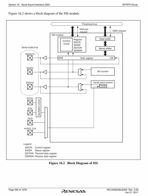
Section 16 Serial Sound Interface (SSI)
Page 592 of 1278 R01UH0234EJ0300 Rev. 3.00 Jun 21, 2011
SH7670 Group
Figure 16.2 shows a block diagram of the SSI module.
SSISCK
SSIWS
SSIDATA
Serial audio bus
RegisterSSICRSSISRSSITDRSSIRDR
SSI module
DMA requestInterruptrequest
Peripheral bus
Data buffer
Barrel shifter
Controlcircuit
Bit counter
Serial clock controlDivider
LSBMSB Shift register
CKIO
Osc
illat
ion
circ
uitEXTAL
XTAL
AUDIO_CLK
SSICR:SSISR:SSITDR:SSIRDR:
Control registerStatus registerTransmit data registerReceive data register
Legend:
Figure 16.2 Block Diagram of SSI

Section 16 Serial Sound Interface (SSI)
R01UH0234EJ0300 Rev. 3.00 Page 593 of 1278 Jun 21, 2011
SH7670 Group
16.2 Input/Output Pins
Table 16.1 shows the pin assignments relating to the SSI module.
Table 16.1 Pin Assignments
Pin Name Number of Pins I/O Description
SSISCK0 1 I/O Serial bit clock
SSIWS0 1 I/O Word selection
SSIDATA0 1 I/O Serial data input/output
SSISCK1 1 I/O Serial bit clock
SSIWS1 1 I/O Word selection
SSIDATA1 1 I/O Serial data input/output
AUDIO_CLK 1 Input External clock for audio (entering oversampling clock 256/384/512fs)

Section 16 Serial Sound Interface (SSI)
Page 594 of 1278 R01UH0234EJ0300 Rev. 3.00 Jun 21, 2011
SH7670 Group
16.3 Register Description
The SSI has the following registers. Note that explanation in the text does not refer to the channels.
Table 16.2 Register Description
Channel Register Name Abbrevia-tion R/W Initial Value Address
Access Size
Control register 0 SSICR_0 R/W H'00000000 H'FFFEC000 32
Status register 0 SSISR_0 R/W* H'02000003 H'FFFEC004 32
Transmit data register 0 SSITDR_0 R/W H'00000000 H'FFFEC008 32
0
Receive data register 0 SSIRDR_0 R H'00000000 H'FFFEC00C 32
Control register 1 SSICR_1 R/W H'00000000 H'FFFEC800 32
Status register 1 SSISR_1 R/W* H'02000003 H'FFFEC804 32
Transmit data register 1 SSITDR_1 R/W H'00000000 H'FFFEC808 32
1
Receive data register 1 SSIRDR_1 R H'00000000 H'FFFEC80C 32
0 SSI clock selection register 0 SCSR_0 R/W H'0000 H'FFFF0000 16
1 SSI clock selection register 1 SCSR_1 R/W H'0000 H'FFFF0800 16
Note: * Although bits 26 and 27 in this register can be read from or written to, bits other than these are read-only. For details, refer to section 16.3.2, Status Register (SSISR).
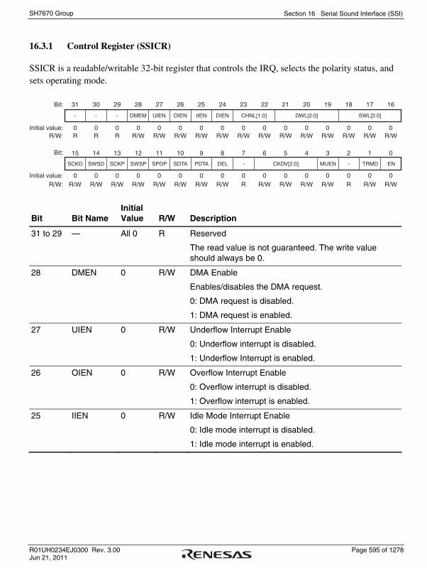
Section 16 Serial Sound Interface (SSI)
R01UH0234EJ0300 Rev. 3.00 Page 595 of 1278 Jun 21, 2011
SH7670 Group
16.3.1 Control Register (SSICR)
SSICR is a readable/writable 32-bit register that controls the IRQ, selects the polarity status, and sets operating mode.
31 30 29 28 27 26 25 24 23 22 21 20 19 18 17 16
15 14 13 12 11 10 9 8 7 6 5 4 3 2 1 0
0 0 0 0 0 0 0 0 0 0 0 0 0 0 0 0R R R R/W R/W R/W R/W R/W R/W R/W R/W R/W R/W R/W R/W R/W
0 0 0 0 0 0 0 0 0 0 0 0 0 0 0 0R/W R/W R/W R/W R/W R/W R/W R/W R R/W R/W R/W R/W R R/W R/W
Bit:
Initial value:R/W:
Bit:
Initial value:R/W:
- - - DMEM UIEN OIEN IIEN DIEN CHNL[1:0] DWL[2:0] SWL[2:0]
SCKD SWSD SCKP SWSP SPDP SDTA PDTA DEL - CKDV[2:0] MUEN - TRMD EN
Bit Bit Name Initial Value R/W Description
31 to 29 — All 0 R Reserved
The read value is not guaranteed. The write value should always be 0.
28 DMEN 0 R/W DMA Enable
Enables/disables the DMA request.
0: DMA request is disabled.
1: DMA request is enabled.
27 UIEN 0 R/W Underflow Interrupt Enable
0: Underflow interrupt is disabled.
1: Underflow Interrupt is enabled.
26 OIEN 0 R/W Overflow Interrupt Enable
0: Overflow interrupt is disabled.
1: Overflow interrupt is enabled.
25 IIEN 0 R/W Idle Mode Interrupt Enable
0: Idle mode interrupt is disabled.
1: Idle mode interrupt is enabled.

Section 16 Serial Sound Interface (SSI)
Page 596 of 1278 R01UH0234EJ0300 Rev. 3.00 Jun 21, 2011
SH7670 Group
Bit Bit Name Initial Value R/W Description
24 DIEN 0 R/W Data Interrupt Enable
0: Data interrupt is disabled.
1: Data interrupt is enabled.
23, 22 CHNL[1:0] 00 R/W Channels
These bits show the number of channels in each system word.
00: Having one channel per system word
01: Having two channels per system word
10 Having three channels per system word
11: Having four channels per system word
21 to 19 DWL[2:0] 000 R/W Data Word Length
Indicates the number of bits in a data word.
000: 8 bits
001: 16 bits
010: 18 bits
011: 20 bits
100: 22 bits
101: 24 bits
110: 32 bits
111: Reserved
18 to 16 SWL[2:0] 000 R/W System Word Length
Indicates the number of bits in a system word.
000: 8 bits
001: 16 bits
010: 24 bits
011: 32 bits
100: 48 bits
101: 64 bits
110: 128 bits
111: 256 bits
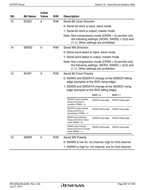
Section 16 Serial Sound Interface (SSI)
R01UH0234EJ0300 Rev. 3.00 Page 597 of 1278 Jun 21, 2011
SH7670 Group
Bit Bit Name Initial Value R/W Description
15 SCKD 0 R/W Serial Bit Clock Direction
0: Serial bit clock is input, slave mode.
1: Serial bit clock is output, master mode.
Note: Non-compression mode (CPEN = 0) permits only the following settings: (SCKD, SWSD) = (0,0) and (1,1). Other settings are prohibited.
14 SWSD 0 R/W Serial WS Direction
0: Serial word select is input, slave mode.
1: Serial word select is output, master mode.
Note: Non-compression mode (CPEN = 0) permits only the following settings: (SCKD, SWSD) = (0,0) and (1,1). Other settings are prohibited.
13 SCKP 0 R/W Serial Bit Clock Polarity
0: SSIWS and SSIDATA change at the SSISCK falling edge (sampled at the SCK rising edge).
1: SSIWS and SSIDATA change at the SSISCK rising edge (sampled at the SCK falling edge).
SCKP = 0 SCKP = 1
SSIDATA input sampling timing at the time of reception (TRMD = 0)
SSISCK rising edge SSISCK falling edge
SSIDATA output change timing at the time of transmission (TRMD = 1)
SSISCK falling edge SSISCK rising edge
SSIWS input sampling timing at the time of slave mode (SWSD = 0)
SSISCK rising edge SSISCK falling edge
SSIWS output change timing at the time of master mode (SWSD = 1)
SSISCK falling edge SSISCK rising edge
12 SWSP 0 R/W Serial WS Polarity
0: SSIWS is low for 1st channel, high for 2nd channel.
1: SSIWS is high for 1st channel, low for 2nd channel.

Section 16 Serial Sound Interface (SSI)
Page 598 of 1278 R01UH0234EJ0300 Rev. 3.00 Jun 21, 2011
SH7670 Group
Bit Bit Name Initial Value R/W Description
11 SPDP 0 R/W Serial Padding Polarity
0: Padding bits are low.
1: Padding bits are high.
Note: When MUEN = 1, the padding bit becomes low (the MUTE function takes precedence).
10 SDTA 0 R/W Serial Data Alignment
0: Transmitting and receiving in the order of serial data and padding bits
1: Transmitting and receiving in the order of padding bits and serial data
9 PDTA 0 R/W Parallel Data Alignment
This bit is ignored if CPEN = 1. When the data word length is 32, 16 or 8 bit, this configuration field has no meaning.
This bit applies to SSIRDR in receive mode and SSITDR in transmit mode.
0: Parallel data (SSITDR, SSIRDR) is left-aligned
1: Parallel data (SSITDR, SSIRDR) is right-aligned.
• DWL = 000 (with a data word length of 8 bits), the
PDTA setting is ignored.
All data bits in SSIRDR or SSITDR are used on the audio serial bus. Four data words are transmitted or received at each 32-bit access. The first data word is derived from bits 7 to 0, the second from bits 15 to 8, the third from bits 23 to 16 and the last data word is derived from bits 31 to 24.
• DWL = 001 (with a data word length of 16 bits), the
PDTA setting is ignored.
All data bits in SSIRDR or SSITDR are used on the audio serial bus. Two data words are transmitted or received at each 32-bit access. The first data word is derived from bits 15 to 0 and the second data word is derived from bits 31 to 16.

Section 16 Serial Sound Interface (SSI)
R01UH0234EJ0300 Rev. 3.00 Page 599 of 1278 Jun 21, 2011
SH7670 Group
Bit Bit Name Initial Value R/W Description
9 PDTA 0 R/W • DWL = 010, 011, 100, 101 (with a data word length
of 18, 20, 22 or 24 bits), PDTA = 0 (left-aligned)
The data bits used in SSIRDR or SSITDR are the following:
Bits 31 down to (32 minus the number of bits in the data word length specified by DWL).
That is, If DWL = 011, the data word length is 20 bits; therefore, bits 31 to 12 in either SSIRDR or SSITDR are used. All other bits are ignored or reserved.
• DWL = 010, 011, 100, 101 (with a data word length
of 18, 20, 22 or 24 bits), PDTA = 1 (right-aligned)
The data bits used in SSIRDR or SSITDR are the following:
Bits (the number of bits in the data word length specified by DWL minus 1) to 0
i.e. if DWL = 011, then DWL = 20 and bits 19 to 0 are used in either SSIRDR or SSITDR. All other bits are ignored or reserved.
• DWL = 110 (with a data word length of 32 bits), the
PDTA setting is ignored.
All data bits in SSIRDR or SSITDR are used on the audio serial bus.
8 DEL 0 R/W Serial Data Delay
0: 1 clock cycle delay between SSIWS and SSIDATA
1: No delay between SSIWS and SSIDATA
Note: When CPEN = 1, this bit should be set to 1.
7 ⎯ 0 R Reserved
The read value is undefined. The write value should always be 0.

Section 16 Serial Sound Interface (SSI)
Page 600 of 1278 R01UH0234EJ0300 Rev. 3.00 Jun 21, 2011
SH7670 Group
Bit Bit Name Initial Value R/W Description
6 to 4 CKDV[2:0] 000 R/W Serial Oversampling Clock Division Ratio
Sets the ratio between oversampling clock* and the serial bit clock. When the SCKD bit is 0, the setting of these bits is ignored. The serial bit clock is used in the shift register and is supplied from the SSISCK pin.
000: Serial bit clock frequency = Oversampling clock Frequency/1
001: Serial bit clock frequency = Oversampling clock frequency/2
010: Serial bit clock frequency = Oversampling clock frequency/4
011: Serial bit clock frequency = Oversampling clock frequency/8
100: Serial bit clock frequency = Oversampling clock frequency/16
101: Serial bit clock frequency = Oversampling clock frequency/6
110: Serial bit clock frequency = Oversampling clock frequency/12
111: Setting prohibited
Note: * An oversampling clock is selected by the SCSR_0/SCSR_1 setting.
3 MUEN 0 R/W Mute Enable
0: Module is not muted.
1: Module is muted.
2 ⎯ 0 R Reserved
The read value is undefined. The write value should always be 0.
1 TRMD 0 R/W Transmit/Receive Mode Select
0: Module is in receive mode.
1: Module is in transmit mode.
0 EN 0 R/W SSI Module Enable
0: Module is disabled.
1: Module is enabled.

Section 16 Serial Sound Interface (SSI)
R01UH0234EJ0300 Rev. 3.00 Page 601 of 1278 Jun 21, 2011
SH7670 Group
16.3.2 Status Register (SSISR)
SSISR consists of status flags indicating the operational status of the SSI module and bits indicating the current channel numbers and word numbers.
31 30 29 28 27 26 25 24 23 22 21 20 19 18 17 16
15 14 13 12 11 10 9 8 7 6 5 4 3 2 1 0
0 0 0 0 0 0 1 0 Un-defined
Un-defined
Un-defined
Un-defined
Un-defined
Un-defined
Un-defined
Un-defined
R R R R R/W* R/W* R R R R R R R R R R
Un-defined
Un-defined
Un-defined
Un-defined
Un-defined
Un-defined
Un-defined
Un-defined
Un-defined
Un-defined
Un-defined
Un-defined
0 0 1 1R R R R R R R R R R R R R R R R
Bit:
Initial value:R/W:
Bit:
Initial value:R/W:
Note: * Can be read from or written to. Writing 0 initializes the bit, but writing 1 is ignored.
- - - DMRQ UIRQ OIRQ IIRQ DIRQ - - - - - - - -
- - - - - - - - - - - - CHNO[1:0] SWNO IDST
Bit Bit Name Initial Value R/W Description
31 to 29 — All 0 R Reserved
The read value is not guaranteed. The write value should always be 0.
28 DMRQ 0 R DMA Request Status Flag
This status flag allows the CPU to recognize the value of the DMA request pin on the SSI module.
• TRMD = 0 (Receive mode)
If DMRQ = 1, the SSIRDR has unread data.
If SSIRDR is read, DMRQ = 0 until there is new unread data.
• TRMD = 1 (Transmit mode)
If DMRQ = 1, SSITDR requires data to be written to continue the transmission to the audio serial bus.
Once data is written to SSITDR, DMRQ = 0 until it requires further transmit data.

Section 16 Serial Sound Interface (SSI)
Page 602 of 1278 R01UH0234EJ0300 Rev. 3.00 Jun 21, 2011
SH7670 Group
Bit Bit Name Initial Value R/W Description
27 UIRQ 0 R/W* Underflow Error Interrupt Status Flag
This status flag indicates that data was supplied at a lower rate than was required.
In either case, this bit is set to 1 regardless of the value of the UIEN bit and can be cleared by writing 0 to this bit.
If UIRQ = 1 and UIEN = 1, an interrupt occurs.
• TRMD = 0 (Receive mode)
If UIRQ = 1, SSIRDR was read before there was new unread data indicated by the DMRQ or DIRQ bit. This can lead to the same received sample being stored twice by the host leading to potential corruption of multi-channel data.
• TRMD = 1 (Transmit mode)
If UIRQ = 1, SSITDR did not have data written to it before it was required for transmission. This will lead to the same sample being transmitted once more and a potential corruption of multi-channel data. This is more serious error than a receive mode underflow as the output SSI data results in error.
Note: When underflow error occurs, the current data in the data buffer of this module is transmitted until the next data is filled.

Section 16 Serial Sound Interface (SSI)
R01UH0234EJ0300 Rev. 3.00 Page 603 of 1278 Jun 21, 2011
SH7670 Group
Bit Bit Name Initial Value R/W Description
26 OIRQ 0 R/W* Overflow Error Interrupt Status Flag
This status flag indicates that data was supplied at a higher rate than was required.
In either case this bit is set to 1 regardless of the value of the OIEN bit and can be cleared by writing 0 to this bit.
If OIRQ = 1 and OIEN = 1, an interrupt occurs.
• TRMD = 0 (Receive mode)
If OIRQ = 1, SSIRDR was not read before there was new unread data written to it. This will lead to the loss of a sample and a potential corruption of multi-channel data.
Note: When overflow error occurs, the current data in the data buffer of this module is overwritten by the next incoming data from the SSI interface.
• TRMD = 1 (Transmit mode)
If OIRQ = 1, SSITDR had data written to it before it was transferred to the shift register. This will lead to the loss of a sample and a potential corruption of multi-channel data.
25 IIRQ 1 R Idle Mode Interrupt Status Flag
This interrupt status flag indicates whether the SSI module is in idle state.
This bit is set regardless of the value of the IIEN bit to allow polling.
The interrupt can be masked by clearing IIEN, but cannot be cleared by writing to this bit.
If IIRQ = 1 and IIEN = 1, an interrupt occurs.
0: The SSI module is not in idle state.
1: The SSI module is in idle state.

Section 16 Serial Sound Interface (SSI)
Page 604 of 1278 R01UH0234EJ0300 Rev. 3.00 Jun 21, 2011
SH7670 Group
Bit Bit Name Initial Value R/W Description
24 DIRQ 0 R Data Interrupt Status Flag
This status flag indicates that the module has data to be read or requires data to be written.
In either case this bit is set to 1 regardless of the value of the DIEN bit to allow polling.
The interrupt can be masked by clearing DIEN, but cannot be cleared by writing to this bit.
If DIRQ= 1 and DIEN = 1, an interrupt occurs.
• TRMD = 0 (Receive mode)
0: No unread data in SSIRDR
1: Unread data in SSIRDR
• TRMD = 1 (Transmit mode)
0: Transmit buffer is full.
1: Transmit buffer is empty and requires data to be written to SSITDR.
23 to 4 — Undefined R Reserved
The read value is undefined. The write value should always be 0.
3, 2 CHNO [1:0]
00 R Channel Number
These bits show the current channel number.
• TRMD = 0 (Receive mode)
CHNO indicates which channel the data in SSIRDR currently represents. This value will change as the data in SSIRDR is updated from the shift register.
• TRMD = 1 (Transmit mode)
CHNO indicates which channel is required to be written to SSITDR. This value will change as the data is copied to the shift register, regardless of whether the data is written to SSITDR.
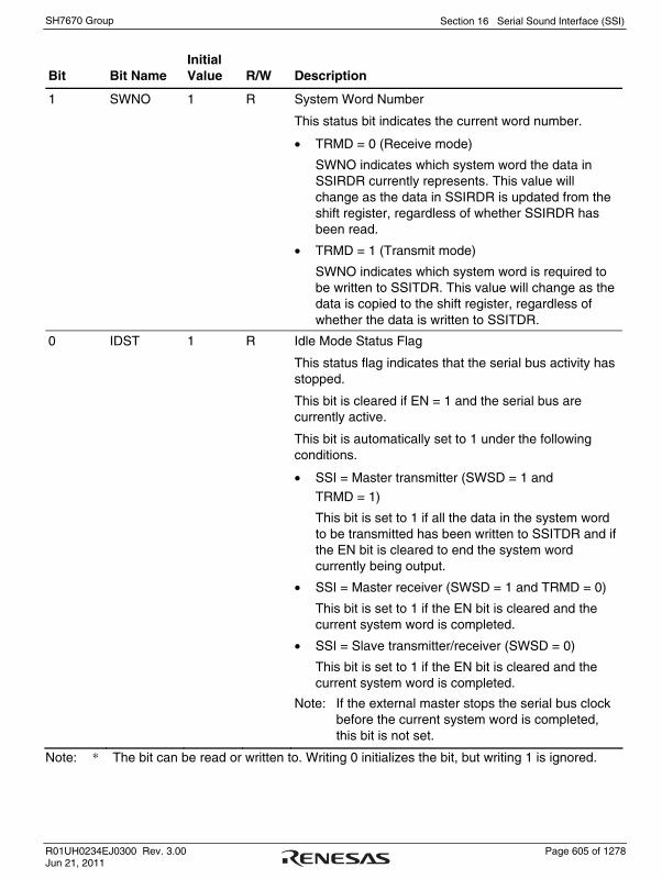
Section 16 Serial Sound Interface (SSI)
R01UH0234EJ0300 Rev. 3.00 Page 605 of 1278 Jun 21, 2011
SH7670 Group
Bit Bit Name Initial Value R/W Description
1 SWNO 1 R System Word Number
This status bit indicates the current word number.
• TRMD = 0 (Receive mode)
SWNO indicates which system word the data in SSIRDR currently represents. This value will change as the data in SSIRDR is updated from the shift register, regardless of whether SSIRDR has been read.
• TRMD = 1 (Transmit mode)
SWNO indicates which system word is required to be written to SSITDR. This value will change as the data is copied to the shift register, regardless of whether the data is written to SSITDR.
0 IDST 1 R Idle Mode Status Flag
This status flag indicates that the serial bus activity has stopped.
This bit is cleared if EN = 1 and the serial bus are currently active.
This bit is automatically set to 1 under the following conditions.
• SSI = Master transmitter (SWSD = 1 and
TRMD = 1)
This bit is set to 1 if all the data in the system word to be transmitted has been written to SSITDR and if the EN bit is cleared to end the system word currently being output.
• SSI = Master receiver (SWSD = 1 and TRMD = 0)
This bit is set to 1 if the EN bit is cleared and the current system word is completed.
• SSI = Slave transmitter/receiver (SWSD = 0)
This bit is set to 1 if the EN bit is cleared and the current system word is completed.
Note: If the external master stops the serial bus clock before the current system word is completed, this bit is not set.
Note: * The bit can be read or written to. Writing 0 initializes the bit, but writing 1 is ignored.

Section 16 Serial Sound Interface (SSI)
Page 606 of 1278 R01UH0234EJ0300 Rev. 3.00 Jun 21, 2011
SH7670 Group
16.3.3 Transmit Data Register (SSITDR)
SSITDR is a 32-bit register that stores data to be transmitted.
Data written to this register is transferred to the shift register upon transmission request. If the data word length is less than 32 bits, the alignment is determined by the setting of the PDTA control bit in SSICR. The data in the buffer can be accessed by reading this register.
31 30 29 28 27 26 25 24 23 22 21 20 19 18 17 16
15 14 13 12 11 10 9 8 7 6 5 4 3 2 1 0
0 0 0 0 0 0 0 0 0 0 0 0 0 0 0 0R/W R/W R/W R/W R/W R/W R/W R/W R/W R/W R/W R/W R/W R/W R/W R/W
0 0 0 0 0 0 0 0 0 0 0 0 0 0 0 0R/W R/W R/W R/W R/W R/W R/W R/W R/W R/W R/W R/W R/W R/W R/W R/W
Bit:
Initial value:R/W:
Bit:
Initial value:R/W:
16.3.4 Receive Data Register (SSIRDR)
SSIRDR is a 32-bit register that stores receive messages.
Data in this register is transferred from the shift register each time data word is received. If the data word length is less than 32 bits, the alignment is determined by the setting of the PDTA control bit in SSICR.
31 30 29 28 27 26 25 24 23 22 21 20 19 18 17 16
15 14 13 12 11 10 9 8 7 6 5 4 3 2 1 0
0 0 0 0 0 0 0 0 0 0 0 0 0 0 0 0R R R R R R R R R R R R R R R R
0 0 0 0 0 0 0 0 0 0 0 0 0 0 0 0R R R R R R R R R R R R R R R R
Bit:
Initial value:R/W:
Bit:
Initial value:R/W:

Section 16 Serial Sound Interface (SSI)
R01UH0234EJ0300 Rev. 3.00 Page 607 of 1278 Jun 21, 2011
SH7670 Group
16.3.5 SSI Clock Selection Register (SCSR)
SCSR is a 16-bit readable/writable register that selects the source of oversampling clocks used by the SSI, as well as division ratio.
15 14 13 12 11 10 9 8 7 6 5 4 3 2 1 0Bit:
Initial Value:R/W:
Note: n=0, 1
0 0 0 0 0 0 0 0 0 0 0 0 0 0 0 0R R R R R R R R R R R R R R/W R/W R/W
⎯ ⎯ ⎯ ⎯⎯ ⎯ ⎯ ⎯ ⎯ ⎯ ⎯ ⎯⎯ SSInCKS[2:0]
Bit Bit Name Initial Value R/W Description
15 to 3 — All 0 R Reserved
The read value is undefined. The write value should always be 0.
2 to 0 SSInCKS[2:0] 000 R/W SSIchn Clock Select
Selects the source of the oversampling clock used by SSIchn. See table 16.3.
Note: n = 0, 1
Table 16.3 Selection of the Source for the Oversampling Clock Used by SSInCKS
Clock Operating Mode SSInCKS[2:0]*1 Setting 0 or 1 2 3
000 Reserved. This is given as an initial value and it should be changed to an appropriate value before SSI operation.
001 Reserved
010 AUDIO_CLK input *2
011 AUDIO_CLK input *2/4
100 EXTAL input CKIO input Setting prohibited
101 EXTAL input /4 CKIO input /4 Setting prohibited
110 EXTAL input /2 CKIO input /2 Setting prohibited
111 EXTAL input /8 CKIO input /8 Setting prohibited
Note: *1. n = 0, 1
*2. Using AUDIO_CLK requires the setting of the control register of the corresponding port.

Section 16 Serial Sound Interface (SSI)
Page 608 of 1278 R01UH0234EJ0300 Rev. 3.00 Jun 21, 2011
SH7670 Group
16.4 Operation Description
16.4.1 Bus Format
The SSI module can operate as a transmitter or a receiver and can be configured into many serial bus formats in either mode.
The bus format can be selected from one of the modes shown in table 16.4.
Table 16.4 Bus Format for SSI Module
Non-Compressed Slave Receiver
Non-Compressed Slave Transmitter
Non-Compressed Master Receiver
Non-Compressed Master Transmitter
TRMD 0 1 0 1
CPEN 0 0 0 0
SCKD 0 0 1 1
SWSD 0 0 1 1
EN
MUEN
DIEN
IIEN
OIEN
UIEN
Control Bits
DEL
PDTA
SDTA
SPDP
SWSP
SCKP
SWL[2:0]
DWL[2:0]
CHNL[1:0]
Configuration Bits

Section 16 Serial Sound Interface (SSI)
R01UH0234EJ0300 Rev. 3.00 Page 609 of 1278 Jun 21, 2011
SH7670 Group
16.4.2 Non-Compressed Modes
The non-compressed modes support all serial audio streams split into channels. It supports Philips, Sony and Matsushita modes as well as many more variants on these modes.
(1) Slave Receiver
This mode allows the module to receive serial data from another device. The clock and word select signal used for the serial data stream is also supplied from an external device. If these signals do not conform to the format specified in the configuration fields of the SSI module, operation is not guaranteed.
(2) Slave Transmitter
This mode allows the module to transmit serial data to another device. The clock and word select signal used for the serial data stream is also supplied from an external device. If these signals do not conform to the format specified in the configuration fields of the SSI module, operation is not guaranteed.
(3) Master Receiver
This mode allows the module to receive serial data from another device. The clock and word select signals are internally derived from the oversampling clock. The format of these signals is defined in the configuration fields of the SSI module. If the incoming data does not follow the configured format, operation is not guaranteed.
(4) Master Transmitter
This mode allows the module to transmit serial data to another device. The clock and word select signals are internally derived from the oversampling clock. The format of these signals is defined in the configuration fields of the SSI module.
(5) Operating Setting Related to Word Length
All bits related to the SSICR's word length are valid in non-compressed modes. There are many configurations the SSI module supports, but some of the combinations are shown below for the popular formats by Philips, Sony, and Matsushita.

Section 16 Serial Sound Interface (SSI)
Page 610 of 1278 R01UH0234EJ0300 Rev. 3.00 Jun 21, 2011
SH7670 Group
• Philips Format
Figures 16.3 and 16.4 demonstrate the supported Philips format both with and without padding. Padding occurs when the data word length is smaller than the system word length.
prev. sample MSB LSB+ 1 LSB MSB LSB
+ 1 LSB next sample
System word 1 =data word 1
System word 2 =data word 2
SSISCK
SSIWS
SSIDATA
SCKP = 0, SWSP = 0, DEL = 0, CHNL = 00System word length = data word length
Figure 16.3 Philips Format (without Padding)
MSB LSB MSB LSB Next
System word 1 System word 2
Data word 1 Data word 2Padding Padding
SSISCK
SSIWS
SSIDATA
SCKP = 0, SWSP = 0, DEL = 0, CHNL = 00, SPDP = 0, SDTA = 0System word length > data word length
Figure 16.4 Philips Format (with Padding)
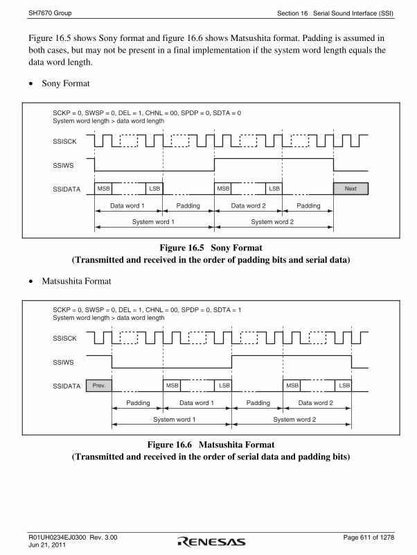
Section 16 Serial Sound Interface (SSI)
R01UH0234EJ0300 Rev. 3.00 Page 611 of 1278 Jun 21, 2011
SH7670 Group
Figure 16.5 shows Sony format and figure 16.6 shows Matsushita format. Padding is assumed in both cases, but may not be present in a final implementation if the system word length equals the data word length.
• Sony Format
MSB LSB MSB LSB Next
SSISCK
SSIWS
SSIDATA
SCKP = 0, SWSP = 0, DEL = 1, CHNL = 00, SPDP = 0, SDTA = 0System word length > data word length
System word 1 System word 2
Data word 1 Data word 2Padding Padding
Figure 16.5 Sony Format (Transmitted and received in the order of padding bits and serial data)
• Matsushita Format
MSB LSB
System word 1 System word 2
Data word 1 Data word 2PaddingPadding
MSB LSBPrev.
SSISCK
SSIWS
SSIDATA
SCKP = 0, SWSP = 0, DEL = 1, CHNL = 00, SPDP = 0, SDTA = 1System word length > data word length
Figure 16.6 Matsushita Format (Transmitted and received in the order of serial data and padding bits)

Section 16 Serial Sound Interface (SSI)
Page 612 of 1278 R01UH0234EJ0300 Rev. 3.00 Jun 21, 2011
SH7670 Group
(6) Multi-channel Formats
Some devices extend the definition of the specification by Philips and allow more than 2 channels to be transferred within two system words.
The SSI module supports the transfer of 4, 6 and 8 channels by using the CHNL, SWL and DWL bits only when the system word length (SWL) is greater than or equal to the data word length (DWL) multiplied by channels (CHNL).
Table 16.5 shows the number of padding bits for each of the valid setting. If setting is not valid, “⎯” is indicated instead of a number.
Table 16.5 The Number of Padding Bits for Each Valid Setting
Padding Bits Per System Word DWL[2:0] 000 001 010 011 100 101 110
CHNL [1:0]
Decoded Channels per System Word
SWL [2:0]
Decoded Word Length 8 16 18 20 22 24 32
000 8 0 ⎯ ⎯ ⎯ ⎯ ⎯ ⎯
001 16 8 0 ⎯ ⎯ ⎯ ⎯ ⎯
010 24 16 8 6 4 2 0 ⎯
011 32 24 16 14 12 10 8 0
100 48 40 32 30 28 26 24 16
101 64 56 48 46 44 42 40 32
110 128 120 112 110 108 106 104 96
00 1
111 256 248 240 238 236 234 232 224
000 8 ⎯ ⎯ ⎯ ⎯ ⎯ ⎯ ⎯
001 16 0 ⎯ ⎯ ⎯ ⎯ ⎯ ⎯
010 24 8 ⎯ ⎯ ⎯ ⎯ ⎯ ⎯
011 32 16 0 ⎯ ⎯ ⎯ ⎯ ⎯
100 48 32 16 12 8 4 0 ⎯
101 64 48 32 28 24 20 16 0
110 128 112 96 92 88 84 80 64
01 2
111 256 240 224 220 216 212 208 192

Section 16 Serial Sound Interface (SSI)
R01UH0234EJ0300 Rev. 3.00 Page 613 of 1278 Jun 21, 2011
SH7670 Group
Padding Bits Per System Word DWL[2:0] 000 001 010 011 100 101 110
CHNL [1:0]
Decoded Channels per System Word
SWL [2:0]
Decoded Word Length 8 16 18 20 22 24 32
000 8 ⎯ ⎯ ⎯ ⎯ ⎯ ⎯ ⎯
001 16 ⎯ ⎯ ⎯ ⎯ ⎯ ⎯ ⎯
010 24 0 ⎯ ⎯ ⎯ ⎯ ⎯ ⎯
011 32 8 ⎯ ⎯ ⎯ ⎯ ⎯ ⎯
100 48 24 0 ⎯ ⎯ ⎯ ⎯ ⎯
101 64 40 16 10 4 ⎯ ⎯ ⎯
110 128 104 80 74 68 62 56 32
10 3
111 256 232 208 202 196 190 184 160
000 8 ⎯ ⎯ ⎯ ⎯ ⎯ ⎯ ⎯
001 16 ⎯ ⎯ ⎯ ⎯ ⎯ ⎯ ⎯
010 24 ⎯ ⎯ ⎯ ⎯ ⎯ ⎯ ⎯
011 32 0 ⎯ ⎯ ⎯ ⎯ ⎯ ⎯
100 48 16 ⎯ ⎯ ⎯ ⎯ ⎯ ⎯
101 64 32 0 ⎯ ⎯ ⎯ ⎯ ⎯
110 128 96 64 56 48 40 32 0
11 4
111 256 224 192 184 176 168 160 128
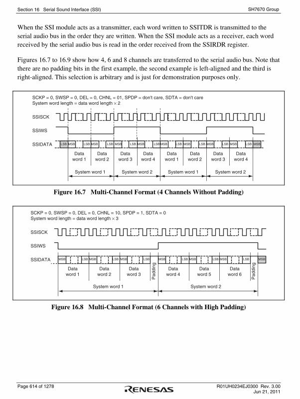
Section 16 Serial Sound Interface (SSI)
Page 614 of 1278 R01UH0234EJ0300 Rev. 3.00 Jun 21, 2011
SH7670 Group
When the SSI module acts as a transmitter, each word written to SSITDR is transmitted to the serial audio bus in the order they are written. When the SSI module acts as a receiver, each word received by the serial audio bus is read in the order received from the SSIRDR register.
Figures 16.7 to 16.9 show how 4, 6 and 8 channels are transferred to the serial audio bus. Note that there are no padding bits in the first example, the second example is left-aligned and the third is right-aligned. This selection is arbitrary and is just for demonstration purposes only.
MSB LSB
Dataword 1
MSB LSB MSB LSB MSB LSB
Dataword 2
Dataword 3
Dataword 4
System word 1 System word 2
MSB LSB
Dataword 1
MSB LSB MSB LSB MSB LSB
Dataword 2
Dataword 3
Dataword 4
System word 1 System word 2
LSB MSB
SSISCK
SSIWS
SSIDATA
SCKP = 0, SWSP = 0, DEL = 0, CHNL = 01, SPDP = don't care, SDTA = don't careSystem word length = data word length × 2
Figure 16.7 Multi-Channel Format (4 Channels Without Padding)
MSB LSB
System word 2
Dataword 1
MSB LSB MSB LSB MSB
Dataword 2
Dataword 3
Pad
ding
System word 1
MSB LSB MSB LSB MSB LSB
Dataword 4
Dataword 5
Dataword 6
SSISCK
SSIWS
SSIDATA
Pad
ding
SCKP = 0, SWSP = 0, DEL = 0, CHNL = 10, SPDP = 1, SDTA = 0System word length = data word length × 3
Figure 16.8 Multi-Channel Format (6 Channels with High Padding)

Section 16 Serial Sound Interface (SSI)
R01UH0234EJ0300 Rev. 3.00 Page 615 of 1278 Jun 21, 2011
SH7670 Group
MSB LSB
System word 2
Dataword 1
MSB LSB MSB LSB MSB LSB MSB LSB MSB LSB MSB LSB MSB LSB
Dataword 2
Dataword 3
Dataword 4
Dataword 5
Dataword 6
Dataword 7
Dataword 8
Pad
ding
System word 1
Pad
ding
SSIWS
SSIDATA
SSISCK
SCKP = 0, SWSP = 0, DEL = 0, CHNL = 11, SPDP = 0, SDTA = 1System word length = data word length × 4
Figure 16.9 Multi-Channel Format (8 Channels; Transmitting and Receiving in the Order of Serial Data and Padding Bits; with Padding)
(7) Bit Setting Configuration Format
Several more configuration bits in non-compressed mode are shown below. These bits are not mutually exclusive, but some combinations may not be useful for any other device.
These configuration bits are described below with reference to figure 16.10.
SSISCK
SSIWS
SSIDATA
Key for this and following diagrams:
0000 00
means a low level on the serial bus (padding or mute)0
means a high level on the serial bus (padding)1
Arrow head indicates sampling point of receiver
Bit n in SSITDRTDn
1st channel 2nd channel
TD28 TD31TD31 TD30 TD29 TD28 TD31 TD30 TD29 TD28
SWL = 6 bits (not attainable in SSI module, demonstration only)DWL = 4 bits (not attainable in SSI module, demonstration only)CHNL = 00, SCKP = 0, SWSP = 0, SPDP = 0, SDTA = 0, PDTA = 0, DEL = 0, MUEN = 04-bit data samples continuously written to SSITDR are transmitted onto the serial audio bus.
Figure 16.10 Basic Sample Format (Transmit Mode with Example System/Data Word Length)

Section 16 Serial Sound Interface (SSI)
Page 616 of 1278 R01UH0234EJ0300 Rev. 3.00 Jun 21, 2011
SH7670 Group
Figure 16.10 uses a system word length of 6 bits and a data word length of 4 bits. These settings are not possible with the SSI module but are used only for clarification of the other configuration bits.
• Inverted Clock
SSISCK
SSIWS
SSIDATA 0000 00
1st Channel 2nd Channel
TD28 TD31TD31 TD30 TD29 TD28 TD31 TD30 TD29 TD28
As basic sample format configuration except SCKP = 1
Figure 16.11 Inverted Clock
• Inverted Word Select
SSISCK
SSIWS
SSIDATA 0000 00
1st Channel 2nd Channel
TD28 TD31TD31 TD30 TD29 TD28 TD31 TD30 TD29 TD28
As basic sample format configuration except SWSP = 1
Figure 16.12 Inverted Word Select
• Inverted Padding Polarity
SSISCK
SSIWS
SSIDATA TD28 TD31
1st Channel 2nd Channel
1 1 1 1 1 1TD31 TD30 TD29 TD28 TD31 TD30 TD29 TD28
As basic sample format configuration except SPDP = 1
Figure 16.13 Inverted Padding Polarity
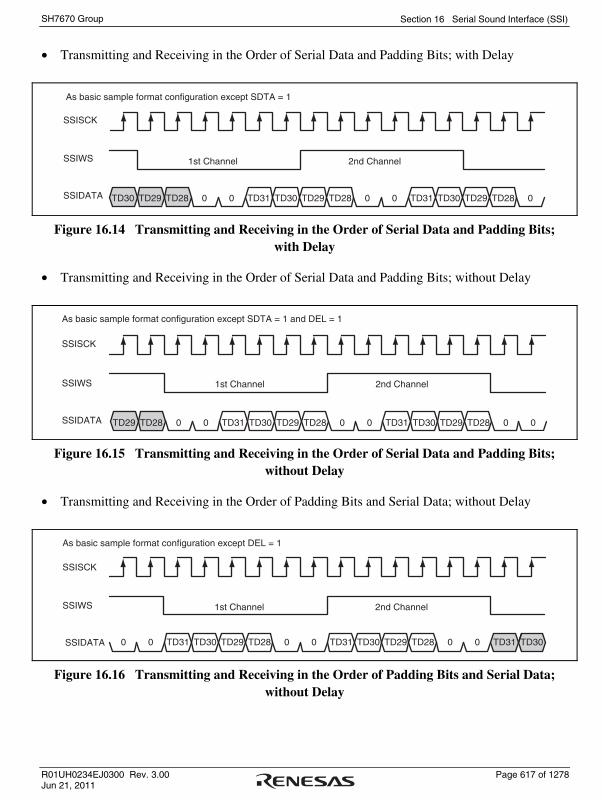
Section 16 Serial Sound Interface (SSI)
R01UH0234EJ0300 Rev. 3.00 Page 617 of 1278 Jun 21, 2011
SH7670 Group
• Transmitting and Receiving in the Order of Serial Data and Padding Bits; with Delay
SSISCK
SSIWS
SSIDATA 000TD28 0 0
1st Channel 2nd Channel
TD30 TD29 TD31 TD30 TD29 TD28 TD31 TD30 TD29 TD28
As basic sample format configuration except SDTA = 1
Figure 16.14 Transmitting and Receiving in the Order of Serial Data and Padding Bits; with Delay
• Transmitting and Receiving in the Order of Serial Data and Padding Bits; without Delay
As basic sample format configuration except SDTA = 1 and DEL = 1
000TD28 0 0TD29 0TD31 TD30 TD29 TD28 TD31 TD30 TD29 TD28
SSISCK
SSIWS
SSIDATA
1st Channel 2nd Channel
Figure 16.15 Transmitting and Receiving in the Order of Serial Data and Padding Bits; without Delay
• Transmitting and Receiving in the Order of Padding Bits and Serial Data; without Delay
As basic sample format configuration except DEL = 1
0000 0 0 TD31 TD30TD31 TD30 TD29 TD28 TD31 TD30 TD29 TD28
SSISCK
SSIWS
SSIDATA
1st Channel 2nd Channel
Figure 16.16 Transmitting and Receiving in the Order of Padding Bits and Serial Data; without Delay
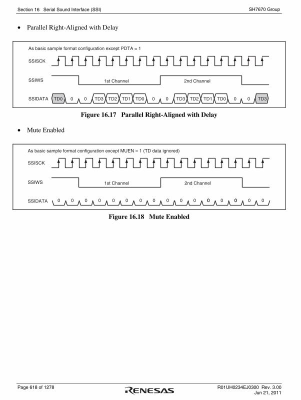
Section 16 Serial Sound Interface (SSI)
Page 618 of 1278 R01UH0234EJ0300 Rev. 3.00 Jun 21, 2011
SH7670 Group
• Parallel Right-Aligned with Delay
As basic sample format configuration except PDTA = 1
0000 0 0 TD3TD0 TD3 TD2 TD1 TD0 TD3 TD2 TD1 TD0
SSISCK
SSIWS
SSIDATA
1st Channel 2nd Channel
Figure 16.17 Parallel Right-Aligned with Delay
• Mute Enabled
As basic sample format configuration except MUEN = 1 (TD data ignored)
0000 0 00 00 00 00 00 000
SSISCK
SSIWS
SSIDATA
1st Channel 2nd Channel
Figure 16.18 Mute Enabled

Section 16 Serial Sound Interface (SSI)
R01UH0234EJ0300 Rev. 3.00 Page 619 of 1278 Jun 21, 2011
SH7670 Group
16.4.3 Operation Modes
There are three modes of operation: configuration, enabled and disabled. Figure 16.19 shows how the module enters each of these modes.
Moduleconfiguration(after reset)
Moduleenabled
(normal tx/rx)
EN = 1(IDST = 0)
Moduledisabled
(waiting untilbus inactive) EN = 0
(IDST = 0)
EN = 0(IDST = 1)
Reset
Figure 16.19 Operation Modes
(1) Configuration Mode
This mode is entered after the module is released from reset. All required configuration fields in the control register should be defined in this mode, before the SSI module is enabled by setting the EN bit.
Setting the EN bit causes the module to enter the module enabled mode.
(2) Module Enabled Mode
Operation of the module in this mode is dependent on the operation mode selected. For details, refer to section 16.4.4, Transmit Operation and section 16.4.5, Receive Operation, below.

Section 16 Serial Sound Interface (SSI)
Page 620 of 1278 R01UH0234EJ0300 Rev. 3.00 Jun 21, 2011
SH7670 Group
16.4.4 Transmit Operation
Transmission can be controlled either by DMA or interrupt.
DMA control is preferred to reduce the processor load. In DMA control mode the processor will only receive interrupts if there is an underflow or overflow of data or the DMAC has finished its transfer.
The alternative method is using the interrupts that the SSI module generates to supply data as required. This mode has a higher interrupt load as the module is only double buffered and will require data to be written at least every system word period.
When disabling the module, the SSI clock* must remain present until the SSI module is in idle state, indicated by the IIRQ bit.
Figure 16.20 shows the transmit operation in DMA control mode, and figure 16.21 shows the transmit operation in interrupt control mode.
Note: * Input clock from the SSISCK pin when SCKD = 0.
Input clock from the AUDIO_CLK pin when SCKD = 1.

Section 16 Serial Sound Interface (SSI)
R01UH0234EJ0300 Rev. 3.00 Page 621 of 1278 Jun 21, 2011
SH7670 Group
(1) Transmission Using DMA Controller
Start
Enable SSI module, enable DMA,
enable error interrupts.
Wait for interrupt from DMAC or SSI.
SSI error interrupt?
More data to be send?
Disable SSI module, disable DMA,
disable error interrupts, enable Idle interrupt.
Wait for idle interruptfrom SSI module.
End*
Yes
No
No
Yes
Yes
No
EN = 1,DMEN = 1,UIEN = 1, OIEN = 1
EN = 0,DMEN = 0UIEN = 0, OIEN = 0,IIEN = 1
Release from reset, set SSICR configuration bits.
Set up DMA controller to provide transmission data as
required.
DMAC: End of Tx data?
Note: * If the SSI encounters an error interrupt underflow/overflow, go back to the start in the flowchart again.
Define TRMD, EN, SCKD, SWSD, MUEN, DEL, PDTA, SDTA, SPDP, SWSP, SCKP, SWL, DWL, CHNL
Figure 16.20 Transmission Using DMA Controller

Section 16 Serial Sound Interface (SSI)
Page 622 of 1278 R01UH0234EJ0300 Rev. 3.00 Jun 21, 2011
SH7670 Group
(2) Transmission Using Interrupt Data Flow Control
Start
Enable SSI module, enable data interrupts, enable error interrupts.
Wait for interrupt from SSI.
Data interrupt?
More data to be send?
Disable SSI module, disable data interrupts disable error interrupts,
enable Idle interrupt.
Wait for Idle interruptfrom SSI module.
End
No
Yes
Yes
No
EN = 1,DIEN = 1,UIEN = 1, OIEN = 1
Use SSI status register bits to realign data
after underflow/overflow.
EN = 0,DIEN = 0UIEN = 0, OIEN = 0,IIEN = 1
Load data of channel n
For n = ( (CHNL + 1) x 2) Loop
Next channel
Release from reset, set SSICR configuration bits.
Define TRMD, EN, SCKD, SWSD, MUEN, DEL, PDTA, SDTA, SPDP, SWSP, SCKP, SWL, DWL, CHNL.
Figure 16.21 Transmission Using Interrupt Data Flow Control

Section 16 Serial Sound Interface (SSI)
R01UH0234EJ0300 Rev. 3.00 Page 623 of 1278 Jun 21, 2011
SH7670 Group
16.4.5 Receive Operation
Like transmission, reception can be controlled either by DMA or interrupt.
Figures 16.22 and 16.23 show the flow of operation.
When disabling the SSI module, the SSI clock* must be kept supplied until the IIRQ bit is in idle state.
Note: * Input clock from the SSISCK pin when SCKD = 0.
Input clock from the AUDIO_CLK pin when SCKD = 1.
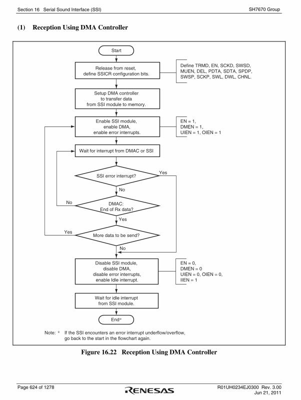
Section 16 Serial Sound Interface (SSI)
Page 624 of 1278 R01UH0234EJ0300 Rev. 3.00 Jun 21, 2011
SH7670 Group
(1) Reception Using DMA Controller
Start
Enable SSI module, enable DMA,
enable error interrupts.
Wait for interrupt from DMAC or SSI
SSI error interrupt?
More data to be send?
Disable SSI module, disable DMA,
disable error interrupts, enable Idle interrupt.
Wait for idle interruptfrom SSI module.
End*
Yes
No
No
Yes
Yes
No
EN = 1,DMEN = 1,UIEN = 1, OIEN = 1
EN = 0,DMEN = 0UIEN = 0, OIEN = 0,IIEN = 1
Setup DMA controllerto transfer data
from SSI module to memory.
Release from reset, define SSICR configuration bits.
DMAC: End of Rx data?
Define TRMD, EN, SCKD, SWSD, MUEN, DEL, PDTA, SDTA, SPDP, SWSP, SCKP, SWL, DWL, CHNL.
Note: * If the SSI encounters an error interrupt underflow/overflow, go back to the start in the flowchart again.
Figure 16.22 Reception Using DMA Controller

Section 16 Serial Sound Interface (SSI)
R01UH0234EJ0300 Rev. 3.00 Page 625 of 1278 Jun 21, 2011
SH7670 Group
(2) Reception Using Interrupt Data Flow Control
Start
Enable SSI module, enable data interrupts, enable error interrupts.
Wait for interrupt from SSI.
Disable SSI module, disable data interrupts, disable error interrupts,
enable idle interrupt.
Wait for idle interrupt from SSI module.
End
Yes
No
Yes
No
EN = 1,DIEN = 1,UIEN = 1, OIEN = 1
Use SSI status register bits to realign data
after underflow/overflow.
EN = 0,DIEN = 0UIEN = 0, OIEN = 0,IIEN = 1
Read data from receive data register.
Release from reset, define SSICR configuration bits.
SSI error interrupt?
Receive more data?
Define TRMD, EN, SCKD, SWSD, MUEN, DEL, PDTA, SDTA, SPDP, SWSP, SCKP, SWL, DWL, CHNL.
Figure 16.23 Reception Using Interrupt Data Flow Control

Section 16 Serial Sound Interface (SSI)
Page 626 of 1278 R01UH0234EJ0300 Rev. 3.00 Jun 21, 2011
SH7670 Group
When an underflow or overflow error condition has matched, the CHNO[1:0] bits and the SWNO bit can be used to recover the SSI module to a known status. When an underflow or overflow occurs, the host can read the channel number and system word number to determine what point the serial audio stream has reached. In the transmitter case, the host can skip forward through the data it wants to transmit until it finds the sample data that matches what the SSI module is expecting to transmit next, and so resynchronize with the audio data stream. In the receiver case the host CPU can store null data to make the number of receive data items consistent until it is ready to store the sample data that the SSI module is indicating will be received next, and so resynchronize with the audio data stream.
16.4.6 Temporary Stop and Restart Procedures in Transmit Mode
The following procedures can be used for implementation.
(1) Procedure for the transfer and stop without having to reconfigure the bus bridge (BBG)/DMAC
1. Set SSICR.DMEN = 0 (disabling a DMA request) to stop the DMA transfer.
2. Wait for SSISR.DIRQ = 1 (transmit mode: the transmit buffer is empty) using a polling, interrupt, or the like.
3. With SSICR.EN = 0 (disabling an SSI module operation), stop the transfer.
4. Before attempting another transfer, make sure that SSISR.IDST = 1 is reached.
5. Set SSICR.EN = 1 (enabling an SSI module operation).
6. Wait for SSISR.DIRQ = 1, using a polling, interrupt, or the like.
7. Setting SSICR.DMEN = 1 (enabling a DMA request) will restart the DMA transfer. (2) Procedure for Reconfiguring the BBG/DMAC after an SSI stop
1. Set SSICR.DMEN = 0 (disabling a DMA request) to stop the DMA transfer.
2. Wait for SSISR.DIRQ = 1 (transmit mode: the transmit buffer is empty), using a polling, interrupt, or the like.
3. With SSICR.EN = 0 (disabling an SSI module operation), stop the transfer.
4. Bring the DMAC to a forced stop with the DSTPR of BBG/DMAC.
5. Before attempting another transfer, make sure that SSISR.IDST = 1 is reached.
6. Set SSICR.EN = 1 (enabling an SSI module operation).
7. Set the BBG/DMAC registers and start the transfer.
8. Setting SSICR.DMEN = 1 (enabling a DMA request) will restart the DMA transfer.

Section 16 Serial Sound Interface (SSI)
R01UH0234EJ0300 Rev. 3.00 Page 627 of 1278 Jun 21, 2011
SH7670 Group
16.4.7 Serial Bit Clock Control
This function is used to control and select which clock is used for the serial bus interface.
If the serial clock direction is set to input (SCKD = 0), the SSI module is in clock slave mode and the shift register uses the bit clock that was input to the SSISCK pin.
If the serial clock direction is set to output (SCKD = 1), the SSI module is in clock master mode, and the shift register uses the bit clock that was input from the AUDIO_CLK pin, or the bit clock that is generated by dividing them. This input clock is then divided by the ratio in the serial oversampling clock divide ratio (CKDV) in SSICR and used as the bit clock in the shift register.
In either case the module pin, SSISCK, is the same as the bit clock.
Section 16 Serial Sound Interface (SSI)
Page 628 of 1278 R01UH0234EJ0300 Rev. 3.00 Jun 21, 2011
SH7670 Group
16.5 Usage Notes
16.5.1 Limitations from Overflow during Receive DMA Operation
If an overflow occurs while the receive DMA is in operation, the module should be restarted. The receive buffer in the SSI consists of 32-bit registers that share the L and R channels. Therefore, data to be received at the L channel may sometimes be received at the R channel if an overflow occurs, for example, under the following condition: the control register (SSICR) has a 32-bit setting for both data word length (DWL2 to DWL0) and system word length (SWL2 to SWL).
If an overflow is confirmed with the overflow error interrupt or overflow error status flag (the OIRQ bit in SSISR), write 0 to the EN bit in SSICR and DMEN bit to disable DMA in the SSI module, thus stopping the operation. (In this case, the controller setting should also be stopped.) After this, write 0 to the OIRQ bit to clear the overflow status, set DMA again and restart the transfer.

Section 17 USB 2.0 Host/Function Module (USB)
R01UH0234EJ0300 Rev. 3.00 Page 629 of 1278 Jun 21, 2011
SH7670 Group
Section 17 USB 2.0 Host/Function Module (USB)
The USB 2.0 host/function module (USB) is a USB controller which provides capabilities as a USB host controller and USB function controller function. This module supports high-speed transfer defined by USB (universal serial bus) Specification 2.0, full-speed transfer, and low-speed transfer when used as the host controller, and supports high-speed transfer and full-speed transfer when used as the function controller. This module has a USB transceiver and supports all of the transfer types defined by the USB specification.
This module has an 8-Kbyte buffer memory for data transfer, providing a maximum of ten pipes. Any endpoint numbers can be assigned to PIPE1 to PIPE9, based on the peripheral devices or user system for communication.
17.1 Features
(1) Host Controller and Function Controller Supporting USB High-Speed Operation
• The USB host controller and USB function controller are incorporated.
• The USB host controller and USB function controller can be switched by register settings.
• USB transceiver is incorporated. (2) Reduced Number of External Pins and Space-Saving Installation
• The VBUS signal can be directly connected to the input pin of this module.
• On-chip D+ pull-up resistor (during USB function operation)
• On-chip D+ and D- pull-down resistor (during USB host operation)
• On-chip D+ and D- terminal resistor (during high-speed operation)
• On-chip D+ and D- output impedance (during full-speed operation) (3) All Types of USB Transfers Supported
• Control transfer
• Bulk transfer
• Interrupt transfer (high bandwidth transfers not supported)
• Isochronous transfer (high bandwidth transfers not supported)
Section 17 USB 2.0 Host/Function Module (USB)
Page 630 of 1278 R01UH0234EJ0300 Rev. 3.00 Jun 21, 2011
SH7670 Group
(4) Internal Bus Interfaces
• Two DMA interface channels are incorporated. (5) Pipe Configuration
• Up to 8 Kbytes of buffer memory for USB communications are supported
• Up to ten pipes can be selected (including the default control pipe)
• Programmable pipe configuration
• Endpoint numbers can be assigned flexibly to PIPE1 to PIPE9.
• Transfer conditions that can be set for each pipe:
PIPE0: Control transfer (default control pipe: DCP), 64-byte fixed single buffer
PIPE1 and PIPE2: Bulk transfers/isochronous transfer, continuous transfer mode, programmable buffer size (up to 2 Kbytes: double buffer can be specified)
PIPE3 to PIPE5: Bulk transfer, continuous transfer mode, programmable buffer size (up to 2 Kbytes: double buffer can be specified)
PIPE6 to PIPE9: Interrupt transfer, 64-byte fixed single buffer (6) Features of the USB Host Controller
• High-speed transfer (480 Mbps), full-speed transfer (12 Mbps), and low-speed transfer (1.5 Mbps) are supported.
• Communications with multiple peripheral devices connected via a single HUB
• Automatic response to the reset handshake
• Automatic scheduling for SOF and packet transmissions
• Programmable intervals for isochronous and interrupt transfers

Section 17 USB 2.0 Host/Function Module (USB)
R01UH0234EJ0300 Rev. 3.00 Page 631 of 1278 Jun 21, 2011
SH7670 Group
(7) Features of the USB Function Controller
• Both high-speed transfer (480 Mbps) and full-speed transfer (12 Mbps) are supported.
• Automatic recognition of high-speed operation or full-speed operation based on automatic response to the reset handshake
• Control transfer stage control function
• Device state control function
• Auto response function for SET_ADDRESS request
• NAK response interrupt function (NRDY)
• SOF interpolation function (8) Other Features
• Transfer ending function using transaction count
• BRDY interrupt event notification timing change function (BFRE)
• Function that automatically clears the buffer memory after the data for the pipe specified at the DnFIFO (n = 0 or 1) port has been read (DCLRM)
• NAK setting function for response PID generated by end of transfer (SHTNAK)
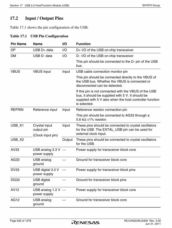
Section 17 USB 2.0 Host/Function Module (USB)
Page 632 of 1278 R01UH0234EJ0300 Rev. 3.00 Jun 21, 2011
SH7670 Group
17.2 Input / Output Pins
Table 17.1 shows the pin configuration of the USB.
Table 17.1 USB Pin Configuration
Pin Name Name I/O Function
DP USB D+ data I/O D+ I/O of the USB on-chip transceiver
DM USB D- data I/O D− I/O of the USB on-chip transceiver
This pin should be connected to the D- pin of the USB bus.
VBUS VBUS input Input USB cable connection monitor pin
This pin should be connected directly to the VBUS of the USB bus. Whether the VBUS is connected or disconnected can be detected.
If this pin is not connected with the VBUS of the USB bus, it should be supplied with 5 V. It should be supplied with 5 V also when the host controller function is selected.
REFRIN Reference input Input Reference resistor connection pin
This pin should be connected to AG33 through a 5.6 kΩ ±1% resistor.
USB_X1 Input These pins should be connected to crystal oscillators for the USB. The EXTAL_USB pin can be used for external clock input.
USB_X2
Crystal input output pin
(Clock input pin) Output These pins should be connected to crystal oscillators
for the USB.
AV33 USB analog 3.3 V power supply
⎯ Power supply for transceiver block core
AG33 USB analog ground
⎯ Ground for transceiver block core
DV33 USB digital 3.3 V power supply
⎯ Power supply for transceiver block pins
DG33 USB digital ground
⎯ Ground for transceiver block pins
AV12 USB analog 1.2 V power supply
⎯ Power supply for transceiver block core
AG12 USB analog ground
⎯ Ground for transceiver block core

Section 17 USB 2.0 Host/Function Module (USB)
R01UH0234EJ0300 Rev. 3.00 Page 633 of 1278 Jun 21, 2011
SH7670 Group
Pin Name Name I/O Function
DV12 USB digital 1.2 V power supply
⎯ Power supply for transceiver block pins
DG12 USB digital ground ⎯ Ground for transceiver block pins
UV12 USB 480 MHz 1.2 V power supply
⎯ Power supply for 480-MHz operation block core
UG12 USB 480 MHz 1.2 V ground
⎯ Ground for 480-MHz operation block core

Section 17 USB 2.0 Host/Function Module (USB)
Page 634 of 1278 R01UH0234EJ0300 Rev. 3.00 Jun 21, 2011
SH7670 Group
17.3 Register Description
Table 17.2 shows the register configuration of the USB. Table 17.3 shows the register state in each processing mode.
Table 17.2 Register Configuration
Register Name Abbreviation R/W Address Access Size
Connection bus
System configuration control register
SYSCFG R/W H'FFFF F800 16
CPU bus wait setting register BUSWAIT R/W H'FFFF F802 16
System configuration status register SYSSTS R H'FFFF F804 16
Device state control register DVSTCTR R/W H'FFFF F808 16
Test mode register TESTMODE R/W H'FFFF F80C
16
DMA0-FIFO bus configuration register
D0FBCFG R/W H'FFFF F810 16
DMA1-FIFO bus configuration register
D1FBCFG R/W H'FFFF F812 16
CFIFO port register CFIFO R/W H'FFFF F814 8/16/32
CFIFO port select register CFIFOSEL R/W H'FFFF F820 16
CFIFO port control register CFIFOCTR R/W H'FFFF F822 16
D0FIFO port select register D0FIFOSEL R/W H'FFFF F828 16
D0FIFO port control register D0FIFOCTR R/W H'FFFF F82A 16
D1FIFO port select register D1FIFOSEL R/W H'FFFF F82C
16
D1FIFO port control register D1FIFOCTR R/W H'FFFF F82E 16
Interrupt enable register 0 INTENB0 R/W H'FFFF F830 16
Interrupt enable register 1 INTENB1 R/W H'FFFF F832 16
BRDY interrupt enable register BRDYENB R/W H'FFFF F836 16
NRDY interrupt enable register NRDYENB R/W H'FFFF F838 16
BEMP interrupt enable register BEMPENB R/W H'FFFF F83A 16
SOF output configuration register SOFCFG R/W H'FFFF F83C
16
Interrupt status register 0 INTSTS0 R/W H'FFFF F840 16
Interrupt status register 1 INTSTS1 R/W H'FFFF F842 16
Peripheral bus

Section 17 USB 2.0 Host/Function Module (USB)
R01UH0234EJ0300 Rev. 3.00 Page 635 of 1278 Jun 21, 2011
SH7670 Group
Register Name Abbreviation R/W Address Access Size
Connection bus
BRDY interrupt status register BRDYSTS R/W H'FFFF F846 16
NRDY interrupt status register NRDYSTS R/W H'FFFF F848 16
BEMP interrupt status register BEMPSTS R/W H'FFFF F84A 16
Frame number register FRMNUM R/W H'FFFF F84C
16
μFrame number register UFRMNUM R/W H'FFFF F84E 16
USB address register USBADDR R H'FFFF F850 16
USB request type register USBREQ R H'FFFF F854 16
USB request value register USBVAL R H'FFFF F856 16
USB request index register USBINDX R H'FFFF F858 16
USB request length register USBLENG R H'FFFF F85A 16
DCP configuration register DCPCFG R/W H'FFFF F85C
16
DCP maximum packet size register DCPMAXP R/W H'FFFF F85E 16
DCP control register DCPCTR R/W H'FFFF F860 16
Pipe window select register PIPESEL R/W H'FFFF F864 16
Pipe configuration register PIPECFG R/W H'FFFF F868 16
Pipe buffer setting register PIPEBUF R/W H'FFFF F86A 16
Pipe maximum packet size register PIPEMAXP R/W H'FFFF F86C
16
Pipe cycle control register PIPEPERI R/W H'FFFF F86E 16
Pipe 1 control register PIPE1CTR R/W H'FFFF F870 16
Pipe 2 control register PIPE2CTR R/W H'FFFF F872 16
Pipe 3 control register PIPE3CTR R/W H'FFFF F874 16
Pipe 4 control register PIPE4CTR R/W H'FFFF F876 16
Pipe 5 control register PIPE5CTR R/W H'FFFF F878 16
Pipe 6 control register PIPE6CTR R/W H'FFFF F87A 16
Pipe 7 control register PIPE7CTR R/W H'FFFF F87C
16
Pipe 8 control register PIPE8CTR R/W H'FFFF F87E 16
Pipe 9 control register PIPE9CTR R/W H'FFFF F880 16
Pipe 1 transaction counter enable register
PIPE1TRE R/W H'FFFF F890 16
Peripheral bus

Section 17 USB 2.0 Host/Function Module (USB)
Page 636 of 1278 R01UH0234EJ0300 Rev. 3.00 Jun 21, 2011
SH7670 Group
Register Name Abbreviation R/W Address Access Size
Connection bus
Pipe 1 transaction counter register PIPE1TRN R/W H'FFFF F892 16
Pipe 2 transaction counter enable register
PIPE2TRE R/W H'FFFF F894 16
Pipe 2 transaction counter register PIPE2TRN R/W H'FFFF F896 16
Pipe 3 transaction counter enable register
PIPE3TRE R/W H'FFFF F898 16
Pipe 3 transaction counter register PIPE3TRN R/W H'FFFF F89A 16
Pipe 4 transaction counter enable register
PIPE4TRE R/W H'FFFF F89C 16
Pipe 4 transaction counter register PIPE4TRN R/W H'FFFF F89E 16
Pipe 5 transaction counter enable register
PIPE5TRE R/W H'FFFF F8A0 16
Pipe 5 transaction counter register PIPE5TRN R/W H'FFFF F8A2 16
Device address 0 configuration register
DEVADD0 R/W H'FFFF F8D0 16
Device address 1 configuration register
DEVADD1 R/W H'FFFF F8D2 16
Device address 2 configuration register
DEVADD2 R/W H'FFFF F8D4 16
Device address 3 configuration register
DEVADD3 R/W H'FFFF F8D6 16
Device address 4 configuration register
DEVADD4 R/W H'FFFF F8D8 16
Device address 5 configuration register
DEVADD5 R/W H'FFFF F8DA 16
Device address 6 configuration register
DEVADD6 R/W H'FFFF F8DC 16
Device address 7 configuration register
DEVADD7 R/W H'FFFF F8DE 16
Device address 8 configuration register
DEVADD8 R/W H'FFFF F8E0 16
Device address 9 configuration register
DEVADD9 R/W H'FFFF F8E2 16
Device address A configuration register
DEVADDA R/W H'FFFF F8E4 16
Peripheral bus

Section 17 USB 2.0 Host/Function Module (USB)
R01UH0234EJ0300 Rev. 3.00 Page 637 of 1278 Jun 21, 2011
SH7670 Group
Register Name Abbreviation R/W Address Access Size
Connection bus
D0FIFO bus wait setting register D0FWAIT R/W H'FFFC 1C0C 16
D1FIFO bus wait setting register D1FWAIT R/W H'FFFC 1C0E 16
D0FIFO port register D0FIFO R/W H'FFFC 1C14 32
D1FIFO port register D1FIFO R/W H'FFFC 1C18 32
Internal bus
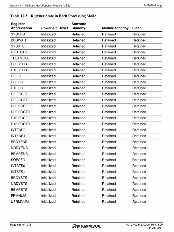
Section 17 USB 2.0 Host/Function Module (USB)
Page 638 of 1278 R01UH0234EJ0300 Rev. 3.00 Jun 21, 2011
SH7670 Group
Table 17.3 Register State in Each Processing Mode
Register Abbreviation Power-On Reset
Software Standby Module Standby Sleep
SYSCFG Initialized Retained Retained Retained
BUSWAIT Initialized Retained Retained Retained
SYSSTS Initialized Retained Retained Retained
DVSTCTR Initialized Retained Retained Retained
TESTMODE Initialized Retained Retained Retained
D0FBCFG Initialized Retained Retained Retained
D1FBCFG Initialized Retained Retained Retained
CFIFO Initialized Retained Retained Retained
D0FIFO Initialized Retained Retained Retained
D1FIFO Initialized Retained Retained Retained
CFIFOSEL Initialized Retained Retained Retained
CFIFOCTR Initialized Retained Retained Retained
D0FIFOSEL Initialized Retained Retained Retained
D0FIFOCTR Initialized Retained Retained Retained
D1FIFOSEL Initialized Retained Retained Retained
D1FIFOCTR Initialized Retained Retained Retained
INTENB0 Initialized Retained Retained Retained
INTENB1 Initialized Retained Retained Retained
BRDYENB Initialized Retained Retained Retained
NRDYENB Initialized Retained Retained Retained
BEMPENB Initialized Retained Retained Retained
SOFCFG Initialized Retained Retained Retained
INTSTS0 Initialized Retained Retained Retained
INTSTS1 Initialized Retained Retained Retained
BRDYSTS Initialized Retained Retained Retained
NRDYSTS Initialized Retained Retained Retained
BEMPSTS Initialized Retained Retained Retained
FRMNUM Initialized Retained Retained Retained
UFRMNUM Initialized Retained Retained Retained

Section 17 USB 2.0 Host/Function Module (USB)
R01UH0234EJ0300 Rev. 3.00 Page 639 of 1278 Jun 21, 2011
SH7670 Group
Register Abbreviation Power-On Reset
Software Standby Module Standby Sleep
USBADDR Initialized Retained Retained Retained
USBREQ Initialized Retained Retained Retained
USBVAL Initialized Retained Retained Retained
USBINDX Initialized Retained Retained Retained
USBLENG Initialized Retained Retained Retained
DCPCFG Initialized Retained Retained Retained
DCPMAXP Initialized Retained Retained Retained
DCPCTR Initialized Retained Retained Retained
PIPESEL Initialized Retained Retained Retained
PIPECFG Initialized Retained Retained Retained
PIPEBUF Initialized Retained Retained Retained
PIPEMAXP Initialized Retained Retained Retained
PIPEPERI Initialized Retained Retained Retained
PIPE1CTR Initialized Retained Retained Retained
PIPE2CTR Initialized Retained Retained Retained
PIPE3CTR Initialized Retained Retained Retained
PIPE4CTR Initialized Retained Retained Retained
PIPE5CTR Initialized Retained Retained Retained
PIPE6CTR Initialized Retained Retained Retained
PIPE7CTR Initialized Retained Retained Retained
PIPE8CTR Initialized Retained Retained Retained
PIPE9CTR Initialized Retained Retained Retained
PIPE1TRE Initialized Retained Retained Retained
PIPE1TRN Initialized Retained Retained Retained
PIPE2TRE Initialized Retained Retained Retained
PIPE2TRN Initialized Retained Retained Retained
PIPE3TRE Initialized Retained Retained Retained
PIPE3TRN Initialized Retained Retained Retained
PIPE4TRE Initialized Retained Retained Retained
PIPE4TRN Initialized Retained Retained Retained

Section 17 USB 2.0 Host/Function Module (USB)
Page 640 of 1278 R01UH0234EJ0300 Rev. 3.00 Jun 21, 2011
SH7670 Group
Register Abbreviation Power-On Reset
Software Standby Module Standby Sleep
PIPE5TRE Initialized Retained Retained Retained
PIPE5TRN Initialized Retained Retained Retained
PHYTEST0 Initialized Retained Retained Retained
PHYTEST1 Initialized Retained Retained Retained
DEVADD0 Initialized Retained Retained Retained
DEVADD1 Initialized Retained Retained Retained
DEVADD2 Initialized Retained Retained Retained
DEVADD3 Initialized Retained Retained Retained
DEVADD4 Initialized Retained Retained Retained
DEVADD5 Initialized Retained Retained Retained
DEVADD6 Initialized Retained Retained Retained
DEVADD7 Initialized Retained Retained Retained
DEVADD8 Initialized Retained Retained Retained
DEVADD9 Initialized Retained Retained Retained
DEVADDA Initialized Retained Retained Retained

Section 17 USB 2.0 Host/Function Module (USB)
R01UH0234EJ0300 Rev. 3.00 Page 641 of 1278 Jun 21, 2011
SH7670 Group
17.3.1 System Configuration Control Register (SYSCFG)
SYSCFG is a register that enables high-speed operation, selects the host controller function or function controller function, controls the DP and DM pins, and enables operation of this module.
This register is initialized by a power-on reset.
15 14 13 12 11 10 9 8 7 6 5 4 3 2 1 0Bit:
Initial value:R/W:
0 0 0 0 0 0 0 0 0 0 0 0 0 0 0 0R R R R R R R R/WR/W R/W R/W R/W R R R R/W
— — — — — — — HSESCKE DCFM DRPD DPRPU — — USBE—
Bit Bit Name Initial Value R/W Description
15 to 11 ⎯ All 0 R Reserved
These bits are always read as 0. The write value should always be 0.
10 SCKE 0 R/W USB Module Clock Enable
Stops or enables supplying 48-MHz clock signal to this module.
0: Stops supplying the clock signal to the USB module.
1: Enables supplying the clock signal to the USB module.
When this bit is 0, only this register and the BUSWAIT register allow both writing and reading.
9, 8 ⎯ All 0 R Reserved
These bits are always read as 0. The write value should always be 0.

Section 17 USB 2.0 Host/Function Module (USB)
Page 642 of 1278 R01UH0234EJ0300 Rev. 3.00 Jun 21, 2011
SH7670 Group
Bit Bit Name Initial Value R/W Description
7 HSE 0 R/W High-Speed Operation Enable
0: High-speed operation is disabled
When the function controller function is selected: Only full-speed operation is enabled.
When the host controller function is selected: Full-speed or low-speed operation is enabled.
1: High-speed operation is enabled (detected by this module)
(1) When the host controller function is selected
When HSE = 0, the USB port performs low-speed or full-speed operation.
Set HSE to 0 when connection of a low-speed peripheral device to the USB port has been detected.
When HSE = 1, this module executes the reset handshake protocol, and automatically allows the USB port to perform high-speed or full-speed operation according to the protocol execution result.
This bit should be modified after detecting device connection (after detecting the ATTCH interrupt) and before executing a USB bus reset (before setting USBRESET to 1).
(2) When the function controller function is selected
When HSE = 0, this module performs full-speed operation.
When HSE = 1, this module executes the reset handshake protocol, and automatically performs high-speed or full-speed operation according to the protocol execution result.
This bit should be modified while DPRPU is 0.
6 DCFM 0 R/W Controller Function Select
Selects the host controller function or function controller function.
0: Function controller function is selected.
1: Host controller function is selected.
This bit should be modified while DPRPU and DPRD are 0.

Section 17 USB 2.0 Host/Function Module (USB)
R01UH0234EJ0300 Rev. 3.00 Page 643 of 1278 Jun 21, 2011
SH7670 Group
Bit Bit Name Initial Value R/W Description
5 DRPD 0 R/W D+/D− Line Resistor Control
Enables or disables pulling down D+ and D- lines when the host controller function is selected.
0: Pulling down the lines is disabled.
1: Pulling down the lines is enabled.
This bit should be set to 1 if the host controller function is selected, and should be set to 0 if the function controller function is selected.
4 DPRPU 0 R/W D+ Line Resistor Control
Enables or disables pulling up D+ line when the function controller function is selected.
0: Pulling up the line is disabled.
1: Pulling up the line is enabled.
Setting this bit to 1 when the function controller function is selected allows this module to pull up the D+ line to 3.3 V, thus notifying the USB host of connection. Modifying this bit from 1 to 0 allows this module to cancel pulling up the D+ line, thus notifying the USB host of disconnection.
This bit should be set to 1 if the function controller function is selected, and should be set to 0 if the host controller function is selected.
3 to 1 ⎯ All 0 R Reserved
These bits are always read as 0. The write value should always be 0.
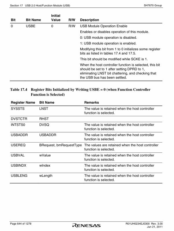
Section 17 USB 2.0 Host/Function Module (USB)
Page 644 of 1278 R01UH0234EJ0300 Rev. 3.00 Jun 21, 2011
SH7670 Group
Bit Bit Name Initial Value R/W Description
0 USBE 0 R/W USB Module Operation Enable
Enables or disables operation of this module.
0: USB module operation is disabled.
1: USB module operation is enabled.
Modifying this bit from 1 to 0 initializes some register bits as listed in tables 17.4 and 17.5.
This bit should be modified while SCKE is 1.
When the host controller function is selected, this bit should be set to 1 after setting DPRD to 1, eliminating LNST bit chattering, and checking that the USB bus has been settled.
Table 17.4 Register Bits Initialized by Writing USBE = 0 (when Function Controller Function is Selected)
Register Name Bit Name Remarks
SYSSTS LNST The value is retained when the host controller function is selected.
DVSTCTR RHST
INTSTS0 DVSQ The value is retained when the host controller function is selected.
USBADDR USBADDR The value is retained when the host controller function is selected.
USEREQ BRequest, bmRequestType The values are retained when the host controller function is selected.
USBVAL wValue The value is retained when the host controller function is selected.
USBINDX wIndex The value is retained when the host controller function is selected.
USBLENG wLength The value is retained when the host controller function is selected.

Section 17 USB 2.0 Host/Function Module (USB)
R01UH0234EJ0300 Rev. 3.00 Page 645 of 1278 Jun 21, 2011
SH7670 Group
Table 17.5 Register Bits Initialized by Writing USBE = 0 (when Host Controller Function is Selected)
Register Name Bit Name Remarks
DVSTCTR RHST
FRMNUM FRNM The value is retained when the function controller function is selected.
UFRMNUM UFRNM The value is retained when the function controller function is selected.
17.3.2 CPU Bus Wait Setting Register (BUSWAIT)
BUSWAIT specifies the number of access waits for those registers of this module that are connected to the peripheral bus (that is, the registers excluding D0FWAIT, D1FWAIT, D0FIFO, and D1FIFO). The basic clock for this module is a USB clock of 48 MHz, and access from the peripheral bus is performed through Pφ synchronization. For this reason, the USB clock must be multiplied by a certain number of cycles when accessing registers of this module via the peripheral bus. The number of access waits should be adjusted to produce at least the approximate value shown below: 83.4 ns (USB clock × 4 cycles) when the size of access is 32 bits, 41.7 ns (USB clock × 2 cycles) when the size of access is 16 bits, or 20.8 ns (USB clock × 1 cycle) when the size of access is 8 bits.
15 14 13 12 11 10 9 8 7 6 5 4 3 2 1 0Bit:
Initial value:R/W:
0 0 0 0 0 0 0 0 0 0 0 1 1R R R R R R R R R R R R R/W R/W R/W R/W
0
— — — — — — — — — — ——
1 1
BWAIT[3:0]
Bit Bit Name Initial Value R/W Description
15 to 4 ⎯ All 0 R Reserved
These bits are always read as 0. The write value should always be 0.

Section 17 USB 2.0 Host/Function Module (USB)
Page 646 of 1278 R01UH0234EJ0300 Rev. 3.00 Jun 21, 2011
SH7670 Group
Bit Bit Name Initial Value R/W Description
3 to 0 BWAIT[3:0] 1111 R/W CPU Bus Wait
On a Pφ basis, set the number of waits needed when accessing registers of this module via the peripheral bus.
0000: 0 wait (accessing two cycles on a Pφ basis)
0001: 1 wait (accessing three cycles on a Pφ basis)
0010: 2 waits (accessing four cycles on a Pφ basis)
:
1111: 15 waits (accessing 17 cycles on a Pφ basis)
Note: Be sure to set this bit in the initialization routine of this module by taking into account the Pφ and access size.
17.3.3 System Configuration Status Register (SYSSTS)
SYSSTS is a register that monitors the line status (D + and D − lines) of the USB data bus.
This register is initialized by a power-on reset or a USB bus reset.
15 14 13 12 11 10 9 8 7 6 5 4 3 2 1 0Bit:
Initial value:R/W:
0 0 0 0 0 0 0 0 0 0 0 0 0R R R R R R R R R R R R R R R R
1
— — — — — — — — — — —— — —
— —
LNST[1:0]
Bit Bit Name Initial Value R/W Description
15 to 11 ⎯ All 0 R Reserved
These bits are always read as 0. The write value should always be 0.
10 ⎯ 1 R Reserved
This bit is always read as 1. The write value should always be 1.
9 to 2 ⎯ All 0 R Reserved
These bits are always read as 0. The write value should always be 0.

Section 17 USB 2.0 Host/Function Module (USB)
R01UH0234EJ0300 Rev. 3.00 Page 647 of 1278 Jun 21, 2011
SH7670 Group
Bit Bit Name Initial Value R/W Description
1, 0 LNST[1:0] Undefined* R USB Data Line Status Monitor
Indicates the status of the USB data bus lines (D+ and D-) as shown in table 17.6.
These bits should be read after setting DPRPU to 1 to notify connection when the function controller function is selected; whereas after setting DRPD to 1 to enable pulling down the lines when the host controller function is selected.
Note: * Depends on the DP and DM pin status.
Table 17.6 USB Data Bus Line Status
LNST[1] LNST[0]
During Low-Speed Operation (only when Host Controller Function is Selected)
During Full-Speed Operation
During High-Speed Operation
During Chirp Operation
0 0 SE0 SE0 Squelch Squelch
0 1 K state J state Not squelch Chirp J
1 0 J state K state Invalid Chirp K
1 1 SE1 SE1 Invalid Invalid
[Legend]
Chirp: The reset handshake protocol is being executed in high-speed operation enabled state (the HSE bit in SYSCFG is set to 1).
Squelch: SE0 or idle state
Not squelch: High-speed J state or high-speed K state Chirp J: Chirp J state
Chirp K: Chirp K state

Section 17 USB 2.0 Host/Function Module (USB)
Page 648 of 1278 R01UH0234EJ0300 Rev. 3.00 Jun 21, 2011
SH7670 Group
17.3.4 Device State Control Register (DVSTCTR)
DVSTCTR is a register that controls and confirms the state of the USB data bus.
This register is initialized by a power-on reset. After a USB bus reset, WKUP is initialized but RESUME is undefined.
15 14 13 12 11 10 9 8 7 6 5 4 3 2 1 0Bit:
Initial value:R/W:
0 0 0 0 0 0 0 0 0 0 0 0 0 0 0 0R R R R R R R R/W* R/W R/W R/W R/W R R R R
— — — — — — — WKUP RWUPE USBRSTRESUME UACT — RHST[2:0]
Bit Bit Name Initial Value R/W Description
15 to 9 ⎯ All 0 R Reserved
These bits are always read as 0. The write value should always be 0.

Section 17 USB 2.0 Host/Function Module (USB)
R01UH0234EJ0300 Rev. 3.00 Page 649 of 1278 Jun 21, 2011
SH7670 Group
Bit Bit Name Initial Value R/W Description
8 WKUP 0 R/W Wakeup Output
Enables or disables outputting the remote wakeup signal (resume signal) to the USB bus when the function controller function is selected.
0: Remote wakeup signal is not output.
1: Remote wakeup signal is output.
The module controls the output time of a remote wakeup signal. When this bit is set to 1, this module clears this bit to 0 after outputting the 10-ms K state.
According to the USB specification, the USB bus idle state must be kept for 5 ms or longer before a remote wakeup signal is output. If this module writes 1 to this bit right after detection of suspended state, the K state will be output after 2 ms.
Note: Do not write 1 to this bit, unless the device state is in the suspended state (the DVSQ bit in the INTSTS0 register is set to 1xx) and the USB host enables the remote wakeup signal. When this bit is set to 1, the internal clock must not be stopped even in the suspended state (write 1 to this bit while SCKE is 1).
This bit should be set to 0 if the host controller function is selected.

Section 17 USB 2.0 Host/Function Module (USB)
Page 650 of 1278 R01UH0234EJ0300 Rev. 3.00 Jun 21, 2011
SH7670 Group
Bit Bit Name Initial Value R/W Description
7 RWUPE 0 R/W Wakeup Detection Enable
Enables or disables the downstream port peripheral device to use the remote wakeup function (resume signal output) when the host controller function is selected.
0: Downstream port wakeup is disabled.
1: Downstream port wakeup is enabled.
With this bit set to 1, on detecting the remote wakeup signal, this module detects the resume signal (K-state for 2.5 μs) from the downstream port device and performs the resume process (drives the port to the K-state).
With this bit set to 0, this module ignores the detected remote wakeup signal (K-state) from the peripheral device connected to the downstream port.
While this bit is 1, the internal clock should not be stopped even in the suspended state (SCKE should be set to 1). Also note that the USB bus should not be reset from the suspended state (USBRST should not be set to 1); it is prohibited by USB Specification 2.0.
This bit should be set to 0 if the function controller function is selected.

Section 17 USB 2.0 Host/Function Module (USB)
R01UH0234EJ0300 Rev. 3.00 Page 651 of 1278 Jun 21, 2011
SH7670 Group
Bit Bit Name Initial Value R/W Description
6 USBRST 0 R/W Bus Reset Output
Controls the USB bus reset signal output when the host controller function is selected.
0: USB bus reset signal is not output.
1: USB bus reset signal is output.
When the host controller function is selected, setting this bit to 1 allows this module to drive the USB port to SE0 to reset the USB bus. Here, this module performs the reset handshake protocol if the HSE bit is 1.
This module continues outputting SE0 while USBRST is 1 (until software sets USBRST to 0). USBRST should be 1 (= USB bus reset period) for the time defined by USB Specification 2.0.
Writing 1 to this bit during communication (UACT = 1) or during the resume process (RESUME = 1) prevents this module from starting the USB bus reset process until both UACT and RESUME become 0.
Write 1 to the UACT bit simultaneously with the end of the USB bus reset process (writing 0 to USBRST).
This bit should be set to 0 if the function controller function is selected.
5 RESUME 0 R/W Resume Output
Controls the resume signal output when the host controller function is selected.
0: Resume signal is not output.
1: Resume signal is output.
Setting this bit to 1 allows this module to drive the port to the K-state and output the resume signal.
This module continues outputting K-state while RESUME is 1 (until software sets RESUME to 0). RESUME should be 1 (= resume period) for the time defined by USB Specification 2.0.
This bit should be set to 1 in the suspended state.
Write 1 to the UACT bit simultaneously with the end of the resume process (writing 0 to RESUME).
This bit should be set to 0 if the function controller function is selected.

Section 17 USB 2.0 Host/Function Module (USB)
Page 652 of 1278 R01UH0234EJ0300 Rev. 3.00 Jun 21, 2011
SH7670 Group
Bit Bit Name Initial Value R/W Description
4 UACT 0 R/W USB Bus Enable
Enables operation of the USB bus (controls the SOF or μSOF packet transmission to the USB bus) when the host controller function is selected.
0: Downstream port is disabled (SOF/μSOF transmission is disabled).
1: Downstream port is enabled (SOF/μSOF transmission is enabled).
With this bit set to 1, this module puts the USB port to the USB-bus enabled state and performs SOF output and data transmission and reception.
This module starts outputting SOF/μSOF within 1 (μ) frame after software has written 1 to UACT.
With this bit set to 0, this module enters the idle state after outputting SOF/μSOF.
This module sets this bit to 0 on any of the following conditions.
• A DTCH interrupt is detected during
communication (while UACT = 1).
• An EOFERR interrupt is detected during
communication (while UACT = 1).
Writing 1 to this bit should be done at the end of the USB reset process (writing 0 to USBRST) or at the end of the resume process from the suspended state (writing 0 to RESUME).
This bit should be set to 0 if the function controller function is selected.
3 ⎯ 0 R Reserved
This bit is always read as 0. The write value should always be 0.

Section 17 USB 2.0 Host/Function Module (USB)
R01UH0234EJ0300 Rev. 3.00 Page 653 of 1278 Jun 21, 2011
SH7670 Group
Bit Bit Name Initial Value R/W Description
2 to 0 RHST[2:0] 000 R Reset Handshake
Indicates the status of the reset handshake.
(1) When the host controller function is selected
000: Communication speed not determined (powered state or no connection)
1xx: Reset handshake in progress
001: Low-speed connection
010: Full-speed connection
011: High-speed connection
These bits indicate 100 after software has written 1 to USBRST.
If HSE has been set to 1, these bits indicate 111 as soon as this module detects Chirp-K from the peripheral device.
This module fixes the value of the RHST bits when software writes 0 to USBRST and this module completes SE0 driving.
(2) When the function controller function is selected
000: Communication speed not determined
100: Reset handshake in progress
010: Full-speed connection
011: High-speed connection
If HSE has been set to 1, these bits indicate 100 as soon as this module detects the USB bus reset. Then, these bits indicate 011 as soon as this module outputs Chirp-K and detects Chirp-JK from the USB host three times. If the connection speed is not fixed to high speed within 2.5 ms after Chirp-K output, these bits indicate 010.
If HSE has been set to 0, these bits indicate 010 as soon as this module detects the USB bus reset.
A DVST interrupt is generated as soon as this module detects the USB bus reset and then the value of the RHST bits is fixed to 010 or 011.
Note: * Only 1 can be written.

Section 17 USB 2.0 Host/Function Module (USB)
Page 654 of 1278 R01UH0234EJ0300 Rev. 3.00 Jun 21, 2011
SH7670 Group
17.3.5 Test Mode Register (TESTMODE)
TESTMODE is a register that controls the USB test signal output during high-speed operation.
This register is initialized by a power-on reset.
15 14 13 12 11 10 9 8 7 6 5 4 3 2 1 0Bit:
Initial value:R/W:
0 0 0 0 0 0 0 0 0 0 0 0 0 0 0 0R R R R R R R R R R R R R/W R/W R/W R/W
— — — — — — — — — — — — UTST[3:0]
Bit Bit Name Initial Value R/W Description
15 to 4 ⎯ All 0 R Reserved
These bits are always read as 0. The write value should always be 0.
3 to 0 UTST[3:0] 0000 R/W Test Mode
This module outputs the USB test signals during the high-speed operation, when these bits are written appropriate value.
Table 17.7 shows test mode operation of this module.
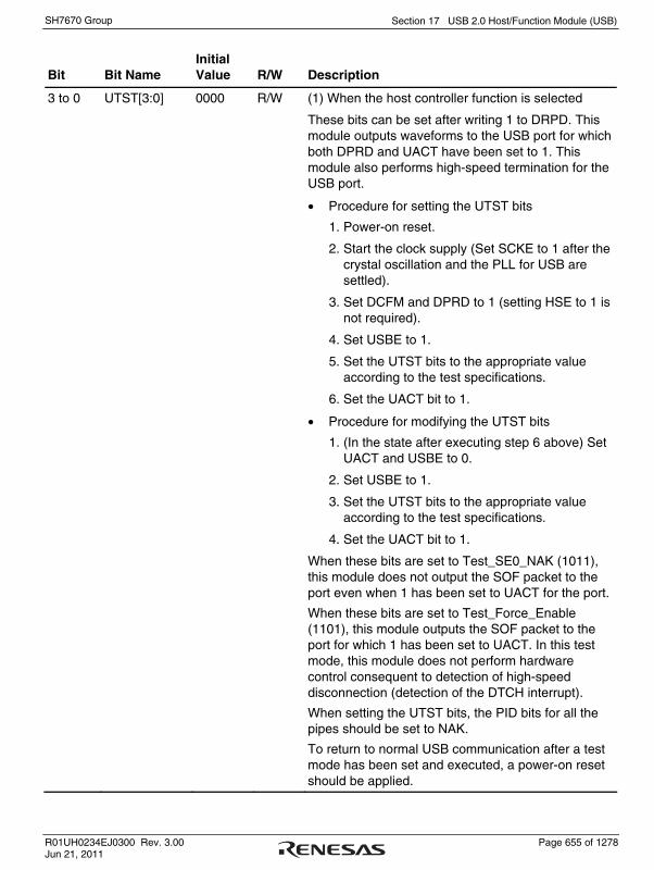
Section 17 USB 2.0 Host/Function Module (USB)
R01UH0234EJ0300 Rev. 3.00 Page 655 of 1278 Jun 21, 2011
SH7670 Group
Bit Bit Name Initial Value R/W Description
3 to 0 UTST[3:0] 0000 R/W (1) When the host controller function is selected
These bits can be set after writing 1 to DRPD. This module outputs waveforms to the USB port for which both DPRD and UACT have been set to 1. This module also performs high-speed termination for the USB port.
• Procedure for setting the UTST bits
1. Power-on reset.
2. Start the clock supply (Set SCKE to 1 after the crystal oscillation and the PLL for USB are settled).
3. Set DCFM and DPRD to 1 (setting HSE to 1 is not required).
4. Set USBE to 1.
5. Set the UTST bits to the appropriate value according to the test specifications.
6. Set the UACT bit to 1.
• Procedure for modifying the UTST bits
1. (In the state after executing step 6 above) Set UACT and USBE to 0.
2. Set USBE to 1.
3. Set the UTST bits to the appropriate value according to the test specifications.
4. Set the UACT bit to 1.
When these bits are set to Test_SE0_NAK (1011), this module does not output the SOF packet to the port even when 1 has been set to UACT for the port.
When these bits are set to Test_Force_Enable (1101), this module outputs the SOF packet to the port for which 1 has been set to UACT. In this test mode, this module does not perform hardware control consequent to detection of high-speed disconnection (detection of the DTCH interrupt).
When setting the UTST bits, the PID bits for all the pipes should be set to NAK.
To return to normal USB communication after a test mode has been set and executed, a power-on reset should be applied.
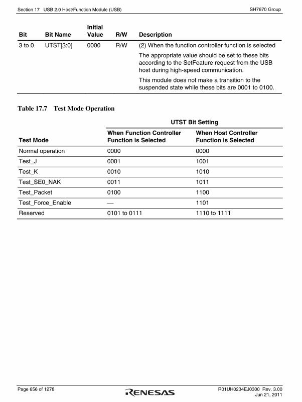
Section 17 USB 2.0 Host/Function Module (USB)
Page 656 of 1278 R01UH0234EJ0300 Rev. 3.00 Jun 21, 2011
SH7670 Group
Bit Bit Name Initial Value R/W Description
3 to 0 UTST[3:0] 0000 R/W (2) When the function controller function is selected
The appropriate value should be set to these bits according to the SetFeature request from the USB host during high-speed communication.
This module does not make a transition to the suspended state while these bits are 0001 to 0100.
Table 17.7 Test Mode Operation
UTST Bit Setting
Test Mode When Function Controller Function is Selected
When Host Controller Function is Selected
Normal operation 0000 0000
Test_J 0001 1001
Test_K 0010 1010
Test_SE0_NAK 0011 1011
Test_Packet 0100 1100
Test_Force_Enable ⎯ 1101
Reserved 0101 to 0111 1110 to 1111

Section 17 USB 2.0 Host/Function Module (USB)
R01UH0234EJ0300 Rev. 3.00 Page 657 of 1278 Jun 21, 2011
SH7670 Group
17.3.6 DMA-FIFO Bus Configuration Registers (D0FBCFG, D1FBCFG)
D0FBCFG is a register that controls DMA0-FIFO bus accesses. D1FBCFG is a register that controls DMA1-FIFO bus accesses.
These registers are initialized by a power-on reset.
15 14 13 12 11 10 9 8 7 6 5 4 3 2 1 0Bit:
Initial value:R/W:
0 0 0 0 0 0 0 0 0 0 0 0 0 0 0 0R R R R R R R R R R R R/W R R R R
— — — — — — — — — TENDE — — — —DFACC
Bit Bit Name Initial Value R/W Description
15, 14 ⎯ All 0 R Reserved
These bits are always read as 0. The write value should always be 0.
13, 12 DFACC 00 R DMAn-FIFO Buffer Access Mode (n = 0, 1)
Specifies DMA0-FIFO or DMA1-FIFO port access mode.
00: Cycle steal mode (initial value)
01: 16-byte continuous access mode
10: 32-byte continuous access mode
11: Invalid
11 to 5 ⎯ All 0 R Reserved
These bits are always read as 0. The write value should always be 0.
4 TENDE 0 R/W DMA Transfer End Sampling Enable
Controls acceptance of the DMA transfer end signal that is transmitted from the DMAC when DMA transfer ends.
0: DMA transfer end signal is not sampled.
1: DMA transfer end signal is sampled.
3 to 0 ⎯ All 0 R Reserved
These bits are always read as 0. The write value should always be 0.

Section 17 USB 2.0 Host/Function Module (USB)
Page 658 of 1278 R01UH0234EJ0300 Rev. 3.00 Jun 21, 2011
SH7670 Group
17.3.7 FIFO Port Registers (CFIFO, D0FIFO, D1FIFO)
CFIFO, D0FIFO and D1FIFO are port registers that are used to read data from the FIFO buffer memory and writing data to the FIFO buffer memory.
There are three FIFO ports: the CFIFO, D0FIFO and D1FIFO ports. Each FIFO port is configured of a port register (CFIFO, D0FIFO, D1FIFO) that handles reading of data from the FIFO buffer memory and writing of data to the FIFO buffer memory, a select register (CFIFOSEL, D0FIFOSEL, D1FIFOSEL) that is used to select the pipe assigned to the FIFO port, and a control register (CFIFOCTR, D0FIFOCTR, D1FIFOCTR).
Each FIFO port has the following features.
• The DCP FIFO buffer should be accessed through the CFIFO port.
• Accessing the FIFO buffer using DMA transfer should be performed through the D0FIFO or D1FIFO port.
• The D1FIFO and D0FIFO ports can be accessed also by the CPU.
• When using functions specific to the FIFO port, the pipe number (selected pipe) specified by the CURPIPE bits cannot be changed (when the DMA transfer function is used, etc.).
• Registers configuring a FIFO port do not affect other FIFO ports.
• The same pipe should not be assigned to two or more FIFO ports.
• There are two FIFO buffer states: the access right is on the CPU side and it is on the SIE side. When the FIFO buffer access right is on the SIE side, the FIFO buffer cannot be accessed from the CPU.
These registers are initialized by a power-on reset.
15 14 13 12 11 10 9 8 7 6 5 4 3 2 1 0Bit:
Initial value:R/W:
0 0 0 0 0 0 0 0 0 0 0 0 0 0 0 0R/W R/W R/W R/W R/W R/W R/W R/W R/W R/W R/W R/W R/W R/W R/W R/W
FIFOPORT[15:0]
31 30 29 28 27 26 25 24 23 22 21 20 19 18 17 16Bit:
Initial value:R/W:
0 0 0 0 0 0 0 0 0 0 0 0 0 0 0 0R/W R/W R/W R/W R/W R/W R/W R/W R/W R/W R/W R/W R/W R/W R/W R/W
FIFOPORT[31:16]

Section 17 USB 2.0 Host/Function Module (USB)
R01UH0234EJ0300 Rev. 3.00 Page 659 of 1278 Jun 21, 2011
SH7670 Group
Bit Bit Name Initial Value R/W Description
31 to 0 FIFOPORT [31:0]
All 0 R/W FIFO Port
Accessing these bits allow reading the received data from the FIFO buffer or writing the transmit data to the FIFO buffer.
These bits can be accessed only while the FRDY bit in each control register (CFIFOCTR, D0FIFOCTR, or D1FIFOCTR) is 1.
The valid bits in this register depend on the settings of the MBW bits (access bit width setting) and BIGEND bit (endian setting) as shown in tables 17.8 to 17.10.
Table 17.8 Endian Operation in 32-Bit Access (when MBW = 10)
BIGEND Bit Bits 31 to 24 Bits 23 to 16 Bits 15 to 8 Bits 7 to 0
0 N + 3 address N + 2 address N + 1 address N + 0 address
1 N + 0 address N + 1 address N + 2 address N + 3 address
Table 17.9 Endian Operation in 16-Bit Access (when MBW = 01)
BIGEND Bit Bits 31 to 24 Bits 23 to 16 Bits 15 to 8 Bits 7 to 0
0 Writing: invalid, reading: prohibited* N + 1 address N + 0 address
1 N + 0 address N + 1 address Writing: invalid, reading: prohibited*
Note: * Reading data from the invalid bits in a word or byte unit is prohibited.
Table 17.10 Endian Operation in 8-Bit Access (when MBW = 00)
BIGEND Bit Bits 31 to 24 Bits 23 to 16 Bits 15 to 8 Bits 7 to 0
0 Writing: invalid, reading: prohibited* N + 0 address
1 N + 0 address Writing: invalid, reading: prohibited*
Note: * Reading data from the invalid bits in a word or byte unit is prohibited.

Section 17 USB 2.0 Host/Function Module (USB)
Page 660 of 1278 R01UH0234EJ0300 Rev. 3.00 Jun 21, 2011
SH7670 Group
17.3.8 FIFO Port Select Registers (CFIFOSEL, D0FIFOSEL, D1FIFOSEL)
CFIFOSEL, D0FIFOSEL and D1FIFOSEL are registers that assign the pipe to the FIFO port, and control access to the corresponding port.
The same pipe should not be specified by the CURPIPE bits in CFIFOSEL, D0FIFOSEL and D1FIFOSEL. When the CURPIPE bits in D0FIFOSEL and D1FIFOSEL are cleared to B'000, no pipe is selected.
The pipe number should not be changed while the DMA transfer is enabled.
These registers are initialized by a power-on reset.
(1) CFIFOSEL
15 14 13 12 11 10 9 8 7 6 5 4 3 2 1 0Bit:
Initial value:R/W:
0 0 0 0 0 0 0 0 0 0 0 0 0 0 0 0R/W R R R/W R/W R R/W R R R/W R R/W R/W R/W R/WR/W*
RCNT REW — — MBW[1:0] — — — ISELBIGEND — CURPIPE[3:0]
Bit Bit Name Initial Value R/W Description
15 RCNT 0 R/W Read Count Mode
Specifies the read mode for the value in the DTLN bits in CFIFOCTR.
0: The DTLN bit is cleared when all of the receive data has been read from the CFIFO.
(In double buffer mode, the DTLN bit value is cleared when all the data has been read from a single plane.)
1: The DTLN bit is decremented when the receive data is read from the CFIFO.
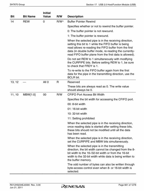
Section 17 USB 2.0 Host/Function Module (USB)
R01UH0234EJ0300 Rev. 3.00 Page 661 of 1278 Jun 21, 2011
SH7670 Group
Bit Bit Name Initial Value R/W Description
14 REW 0 R/W* Buffer Pointer Rewind
Specifies whether or not to rewind the buffer pointer.
0: The buffer pointer is not rewound.
1: The buffer pointer is rewound.
When the selected pipe is in the receiving direction, setting this bit to 1 while the FIFO buffer is being read allows re-reading the FIFO buffer from the first data (in double buffer mode, re-reading the currently-read FIFO buffer plane from the first data is allowed).
Do not set REW to 1 simultaneously with modifying the CURPIPE bits. Before setting REW to 1, be sure to check that FRDY is 1.
To re-write to the FIFO buffer again from the first data for the pipe in the transmitting direction, use the BCLR bit.
13, 12 ⎯ All 0 R Reserved
These bits are always read as 0. The write value should always be 0.
11, 10 MBW[1:0] 00 R/W CFIFO Port Access Bit Width
Specifies the bit width for accessing the CFIFO port.
00: 8-bit width
01: 16-bit width
10: 32-bit width
11: Setting prohibited
When the selected pipe is in the receiving direction, once reading data is started after setting these bits, these bits should not be modified until all the data has been read.
When the selected pipe is in the receiving direction, set the CURPIPE and MBW bits simultaneously.
When the selected pipe is in the transmitting direction, the bit width cannot be changed from the 8-bit width to the 16-/32-bit width or from the 16-bit width to the 32-bit width while data is being written to the buffer memory.
The odd number of bytes can also be written through byte-access control even when 8- or 16-bit width is selected.

Section 17 USB 2.0 Host/Function Module (USB)
Page 662 of 1278 R01UH0234EJ0300 Rev. 3.00 Jun 21, 2011
SH7670 Group
Bit Bit Name Initial Value R/W Description
9 ⎯ 0 R Reserved
This bit is always read as 0. The write value should always be 0.
8 BIGEND 0 R/W CFIFO Port Endian Control
Specifies the byte endian for the CFIFO port.
0: Little endian
1: Big endian
7, 6 ⎯ All 0 R Reserved
These bits are always read as 0. The write value should always be 0.
5 ISEL 0 R/W CFIFO Port Access Direction When DCP is Selected
0: Reading from the buffer memory is selected
1: Writing to the buffer memory is selected
After writing to this bit with the DCP being a selected pipe, read this bit to check that the written value agrees with the read value before proceeding to the next process.
Even if an attempt is made to modify the setting of this bit during access to the FIFO buffer, the current access setting is retained until the access is completed. Then, the modification becomes effective thus enabling continuous access.
Set this bit and the CURPIPE bits simultaneously.
4 ⎯ 0 R Reserved
This bit is always read as 0. The write value should always be 0.
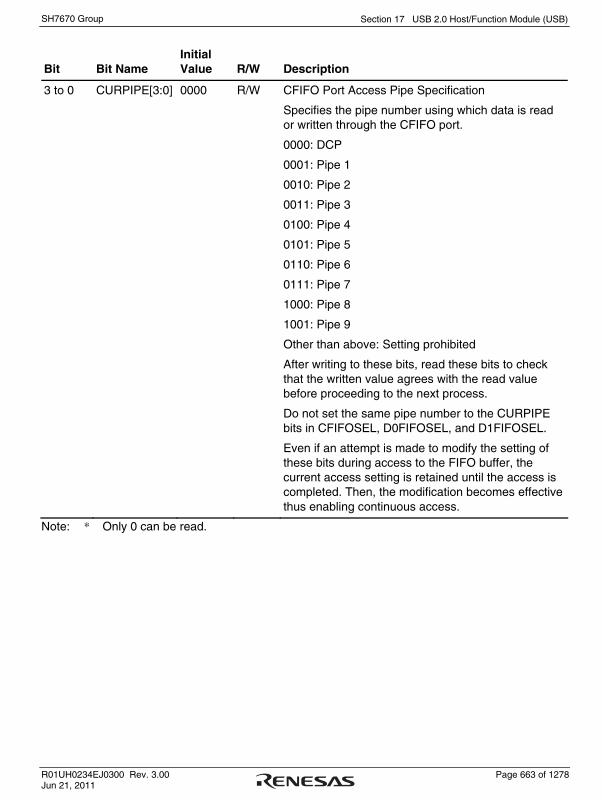
Section 17 USB 2.0 Host/Function Module (USB)
R01UH0234EJ0300 Rev. 3.00 Page 663 of 1278 Jun 21, 2011
SH7670 Group
Bit Bit Name Initial Value R/W Description
3 to 0 CURPIPE[3:0] 0000 R/W CFIFO Port Access Pipe Specification
Specifies the pipe number using which data is read or written through the CFIFO port.
0000: DCP
0001: Pipe 1
0010: Pipe 2
0011: Pipe 3
0100: Pipe 4
0101: Pipe 5
0110: Pipe 6
0111: Pipe 7
1000: Pipe 8
1001: Pipe 9
Other than above: Setting prohibited
After writing to these bits, read these bits to check that the written value agrees with the read value before proceeding to the next process.
Do not set the same pipe number to the CURPIPE bits in CFIFOSEL, D0FIFOSEL, and D1FIFOSEL.
Even if an attempt is made to modify the setting of these bits during access to the FIFO buffer, the current access setting is retained until the access is completed. Then, the modification becomes effective thus enabling continuous access.
Note: * Only 0 can be read.
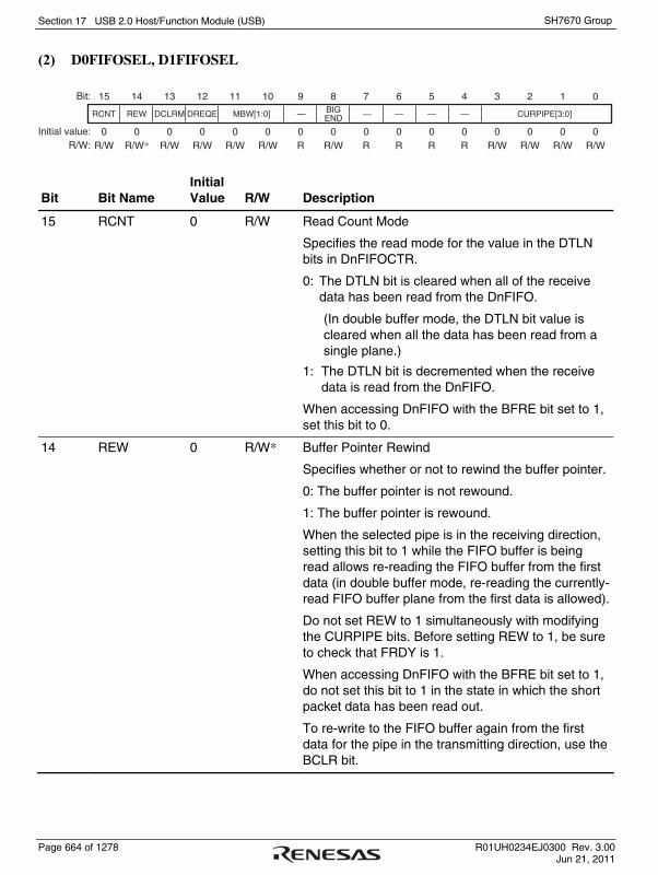
Section 17 USB 2.0 Host/Function Module (USB)
Page 664 of 1278 R01UH0234EJ0300 Rev. 3.00 Jun 21, 2011
SH7670 Group
(2) D0FIFOSEL, D1FIFOSEL
15 14 13 12 11 10 9 8 7 6 5 4 3 2 1 0Bit:
Initial value:R/W:
0 0 0 0 0 0 0 0 0 0 0 0 0 0 0 0R/W R/W* R/W R/W R/W R/W R R/W R R R R R/W R/W R/W R/W
RCNT REW DCLRM DREQE MBW[1:0] BIGEND — — — CURPIPE[3:0]— —
Bit Bit Name Initial Value R/W Description
15 RCNT 0 R/W Read Count Mode
Specifies the read mode for the value in the DTLN bits in DnFIFOCTR.
0: The DTLN bit is cleared when all of the receive data has been read from the DnFIFO.
(In double buffer mode, the DTLN bit value is cleared when all the data has been read from a single plane.)
1: The DTLN bit is decremented when the receive data is read from the DnFIFO.
When accessing DnFIFO with the BFRE bit set to 1, set this bit to 0.
14 REW 0 R/W* Buffer Pointer Rewind
Specifies whether or not to rewind the buffer pointer.
0: The buffer pointer is not rewound.
1: The buffer pointer is rewound.
When the selected pipe is in the receiving direction, setting this bit to 1 while the FIFO buffer is being read allows re-reading the FIFO buffer from the first data (in double buffer mode, re-reading the currently-read FIFO buffer plane from the first data is allowed).
Do not set REW to 1 simultaneously with modifying the CURPIPE bits. Before setting REW to 1, be sure to check that FRDY is 1.
When accessing DnFIFO with the BFRE bit set to 1, do not set this bit to 1 in the state in which the short packet data has been read out.
To re-write to the FIFO buffer again from the first data for the pipe in the transmitting direction, use the BCLR bit.

Section 17 USB 2.0 Host/Function Module (USB)
R01UH0234EJ0300 Rev. 3.00 Page 665 of 1278 Jun 21, 2011
SH7670 Group
Bit Bit Name Initial Value R/W Description
13 DCLRM 0 R/W Auto Buffer Memory Clear Mode Accessed after Specified Pipe Data is Read
Enables or disables the buffer memory to be cleared automatically after data has been read out using the selected pipe.
0: Auto buffer clear mode is disabled.
1: Auto buffer clear mode is enabled.
With this bit set to 1, this module sets BCLR to 1 for the FIFO buffer of the selected pipe on receiving a zero-length packet while the FIFO buffer assigned to the selected pipe is empty, or on receiving a short packet and reading the data while BFRE is 1.
When using this module with the BRDYM bit set to 1, set this bit to 0.
12 DREQE 0 R/W DMA Transfer Request Enable
Enables or disables the DMA transfer request to be issued.
0: Request disabled
1: Request enabled
Before setting this bit to 1 to enable the DMA transfer request to be issued, set the CURPIPE bits.
Before modifying the CURPIPE bit setting, set this bit to 0.
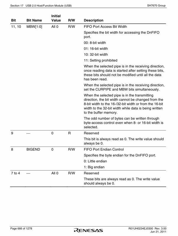
Section 17 USB 2.0 Host/Function Module (USB)
Page 666 of 1278 R01UH0234EJ0300 Rev. 3.00 Jun 21, 2011
SH7670 Group
Bit Bit Name Initial Value R/W Description
11, 10 MBW[1:0] All 0 R/W FIFO Port Access Bit Width
Specifies the bit width for accessing the DnFIFO port.
00: 8-bit width
01: 16-bit width
10: 32-bit width
11: Setting prohibited
When the selected pipe is in the receiving direction, once reading data is started after setting these bits, these bits should not be modified until all the data has been read.
When the selected pipe is in the receiving direction, set the CURPIPE and MBW bits simultaneously.
When the selected pipe is in the transmitting direction, the bit width cannot be changed from the 8-bit width to the 16-/32-bit width or from the 16-bit width to the 32-bit width while data is being written to the buffer memory.
The odd number of bytes can be written through byte-access control even when 8- or 16-bit width is selected.
9 ⎯ 0 R Reserved
This bit is always read as 0. The write value should always be 0.
8 BIGEND 0 R/W FIFO Port Endian Control
Specifies the byte endian for the DnFIFO port.
0: Little endian
1: Big endian
7 to 4 ⎯ All 0 R/W Reserved
These bits are always read as 0. The write value should always be 0.

Section 17 USB 2.0 Host/Function Module (USB)
R01UH0234EJ0300 Rev. 3.00 Page 667 of 1278 Jun 21, 2011
SH7670 Group
Bit Bit Name Initial Value R/W Description
3 to 0 CURPIPE[3:0] 0000 R/W FIFO Port Access Pipe Specification
Specifies the pipe number using which data is read or written through the D0FIFO/D1FIFO port.
0000: No pipe specified
0001: Pipe 1
0010: Pipe 2
0011: Pipe 3
0100: Pipe 4
0101: Pipe 5
0110: Pipe 6
0111: Pipe 7
1000: Pipe 8
1001: Pipe 9
Other than above: Setting prohibited
After writing to these bits, read these bits to check that the written value agrees with the read value before proceeding to the next process.
Do not set the same pipe number to the CURPIPE bits in CFIFOSEL, D0FIFOSEL, and D1FIFOSEL.
Even if an attempt is made to modify the setting of these bits during access to the FIFO buffer, the current access setting is retained until the access is completed. Then, the modification becomes effective thus enabling continuous access.
Note: * Only 0 can be read.
17.3.9 FIFO Port Control Registers (CFIFOCTR, D0FIFOCTR, D1FIFOCTR)
CFIFOCTR, D0FIFOCTR and D1FIFOCTR are registers that determine whether or not writing to the buffer memory has been finished, the buffer accessed from the CPU has been cleared, and the FIFO port is accessible. CFIFOCTR, D0FIFOCTR, and D1FIFOCTR are used for the corresponding FIFO ports.
These registers are initialized by a power-on reset.

Section 17 USB 2.0 Host/Function Module (USB)
Page 668 of 1278 R01UH0234EJ0300 Rev. 3.00 Jun 21, 2011
SH7670 Group
15 14 13 12 11 10 9 8 7 6 5 4 3 2 1 0Bit:
Initial value:R/W:
0 0 0 0 0 0 0 0 0 0 0 0 0 0 0 0R/W*2 R/W*1 R R R R R R R R R R R R R R
BVAL BCLR FRDY — DTLN[11:0]
Bit Bit Name Initial Value R/W Description
15 BVAL 0 R/W*2 Buffer Memory Valid Flag
This bit should be set to 1 when data has been completely written to the FIFO buffer on the CPU side for the pipe selected using the CURPIPE bits (selected pipe).
0: Invalid
1: Writing ended
When the selected pipe is in the transmitting direction, set this bit to 1 in the following cases. Then, this module switches the FIFO buffer from the CPU side to the SIE side, enabling transmission.
• To transmit a short packet, set this bit to 1 after
data has been written.
• To transmit a zero-length packet, set this bit to 1
before data is written to the FIFO buffer.
• Set this bit to 1 after the number of data bytes has been written for the pipe in continuous
transfer mode, where the number is a natural
integer multiple of the maximum packet size and
less than the buffer size.
When the data of the maximum packet size has been written for the pipe in continuous transfer mode, this module sets this bit to 1 and switches the FIFO buffer from the CPU side to the SIE side, enabling transmission.
Writing 1 to this bit should be done while FRDY indicates 1 (set by this module).
When the selected pipe is in the receiving direction, do not set this bit to 1.

Section 17 USB 2.0 Host/Function Module (USB)
R01UH0234EJ0300 Rev. 3.00 Page 669 of 1278 Jun 21, 2011
SH7670 Group
Bit Bit Name Initial Value R/W Description
14 BCLR 0 R/W*1 CPU Buffer Clear
This bit should be set to 1 to clear the FIFO buffer on the CPU side for the selected pipe.
0: Invalid
1: Clears the buffer memory on the CPU side.
When double buffer mode is set for the FIFO buffer assigned to the selected pipe, this module clears only one plane of the FIFO buffer even when both planes are read-enabled.
When the selected pipe is the DCP, setting BCLR to 1 allows this module to clear the FIFO buffer regardless of whether the FIFO buffer is on the CPU side or SIE side. To clear the buffer on the SIE side, set the PID bits for the DCP to NAK before setting BCLR to 1.
When the selected pipe is in the transmitting direction, if 1 is written to BVAL and BCLR bits simultaneously, this module clears the data that has been written before it, enabling transmission of a zero-length packet.
When the selected pipe is not the DCP, writing 1 to this bit should be done while FRDY indicates 1 (set by this module).
13 FRDY 0 R FIFO Port Ready
Indicates whether the FIFO port can be accessed by the CPU (DMAC).
0: FIFO port access is disabled.
1: FIFO port access is enabled.
In the following cases, this module sets FRDY to 1 but data cannot be read via the FIFO port because there is no data to be read. In these cases, set BCLR to 1 to clear the FIFO buffer, and enable transmission and reception of the next data.
• A zero-length packet is received when the FIFO
buffer assigned to the selected pipe is empty.
• A short packet is received and the data is
completely read while BFRE is 1.

Section 17 USB 2.0 Host/Function Module (USB)
Page 670 of 1278 R01UH0234EJ0300 Rev. 3.00 Jun 21, 2011
SH7670 Group
Bit Bit Name Initial Value R/W Description
12 ⎯ 0 R Reserved
This bit is always read as 0. The write value should always be 0.
11 to 0 DTLN[11:0] H'000 R Receive Data Length
Indicates the length of the receive data.
While the FIFO buffer is being read, these bits indicate the different values depending on the RCNT bit value as described below.
• RCNT = 0:
This module sets these bits to indicate the length of the receive data until the CPU (DMAC) has read all the received data from a single FIFO buffer plane.
While BFRE is 1, these bits retain the length of the receive data until BCLR is set to 1 even after all the data has been read.
• RCNT = 1:
This module decrements the value indicated by these bits each time data is read from the FIFO buffer. (The value is decremented by one when MBW is 0, and by two when MBW is 1.)
This module sets these bits to 0 when all the data has been read from one FIFO buffer plane. However, in double buffer mode, if data has been received in one FIFO buffer plane before all the data has been read from the other plane, this module sets these bits to indicate the length of the receive data in the former plane when all the data has been read from the latter plane.
When RCNT is 1, reading these bits while the FIFO buffer is being read returns the latest value within 150 ns after the FIFO port read cycle.
Notes: 1. Only 0 can be read and 1 can be written to. 2. Only 1 can be written to.

Section 17 USB 2.0 Host/Function Module (USB)
R01UH0234EJ0300 Rev. 3.00 Page 671 of 1278 Jun 21, 2011
SH7670 Group
17.3.10 Interrupts Enable Register 0 (INTENB0)
INTENB0 is a register that specifies the various interrupt masks. On detecting the interrupt corresponding to the bit in this register to which software has set 1, this module generates the USB interrupt.
This module sets 1 to each status bit in INTSTS0 when a detection condition of the corresponding interrupt source has been satisfied regardless of the set value in INTENB0 (regardless of whether the interrupt output is enabled or disabled).
While the status bit in INTSTS0 corresponding to the interrupt source indicates 1, this module generates the USB interrupt when software modifies the corresponding interrupt enable bit in INTENB0 from 0 to 1.
This register is initialized by a power-on reset.
15 14 13 12 11 10 9 8 7 6 5 4 3 2 1 0Bit:
Initial value:R/W:
0 0 0 0 0 0 0 0 0 0 0 0 0 0 0 0R/W R/W R/W R/W R/W R/W R/W R/W R R R R R R R R
VBSE RSME SOFE DVSE CTRE BEMPE NRDYE BRDYE — — — — — — — —
Bit Bit Name Initial Value R/W Description
15 VBSE 0 R/W VBUS Interrupts Enable
Enables or disables the USB interrupt output when the VBINT interrupt is detected.
0: Interrupt output disabled
1: Interrupt output enabled
14 RSME 0 R/W Resume Interrupts Enable
Enables or disables the USB interrupt output when the RESM interrupt is detected.
0: Interrupt output disabled
1: Interrupt output enabled

Section 17 USB 2.0 Host/Function Module (USB)
Page 672 of 1278 R01UH0234EJ0300 Rev. 3.00 Jun 21, 2011
SH7670 Group
Bit Bit Name Initial Value R/W Description
13 SOFE 0 R/W Frame Number Update Interrupts Enable
Enables or disables the USB interrupt output when the SOFR interrupt is detected.
0: Interrupt output disabled
1: Interrupt output enabled
12 DVSE 0 R/W Device State Transition Interrupts Enable*
Enables or disables the USB interrupt output when the DVST interrupt is detected.
0: Interrupt output disabled
1: Interrupt output enabled
11 CTRE 0 R/W Control Transfer Stage Transition Interrupts Enable*
Enables or disables the USB interrupt output when the CTRT interrupt is detected.
0: Interrupt output disabled
1: Interrupt output enabled
10 BEMPE 0 R/W Buffer Empty Interrupts Enable
Enables or disables the USB interrupt output when the BEMP interrupt is detected.
0: Interrupt output disabled
1: Interrupt output enabled
9 NRDYE 0 R/W Buffer Not Ready Response Interrupts Enable
Enables or disables the USB interrupt output when the NRDY interrupt is detected.
0: Interrupt output disabled
1: Interrupt output enabled

Section 17 USB 2.0 Host/Function Module (USB)
R01UH0234EJ0300 Rev. 3.00 Page 673 of 1278 Jun 21, 2011
SH7670 Group
Bit Bit Name Initial Value R/W Description
8 BRDYE 0 R/W Buffer Ready Interrupts Enable
Enables or disables the USB interrupt output when the BRDY interrupt is detected.
0: Interrupt output disabled
1: Interrupt output enabled
7 to 0 ⎯ All 0 R Reserved
These bits are always read as 0. The write value should always be 0.
Note: * The RSME, DVSE, and CTRE bits can be set to 1 only when the function controller function is selected; do not set these bits to 1 to enable the corresponding interrupt output when the host controller function is selected.
17.3.11 Interrupt Enable Register 1 (INTENB1)
INTENB1 is a register that specifies the various interrupt masks when the host controller function is selected. On detecting the interrupt corresponding to the bit in this register to which software has set 1, this module generates the USB interrupt.
This module sets 1 to each status bit in INTSTS1 when a detection condition of the corresponding interrupt source has been satisfied regardless of the set value in INTENB1 (regardless of whether the interrupt output is enabled or disabled).
While the status bit in INTSTS1 corresponding to the interrupt source indicates 1, this module generates the USB interrupt when software modifies the corresponding interrupt enable bit in INTENB1 from 0 to 1.
When the function controller function is selected, the interrupts should not be enabled. This register is initialized by a power-on reset.
15 14 13 12 11 10 9 8 7 6 5 4 3 2 1 0Bit:
Initial value:R/W:
0 0 0 0 0 0 0 0 0 0 0 0 0 0 0 0R R/W R R/W R/W R R R R R/W R/W R/W R R R R
— BCHGE — DTCHE ATTCHE — — — EOF
ERRE SIGNE SACKE — — — ——
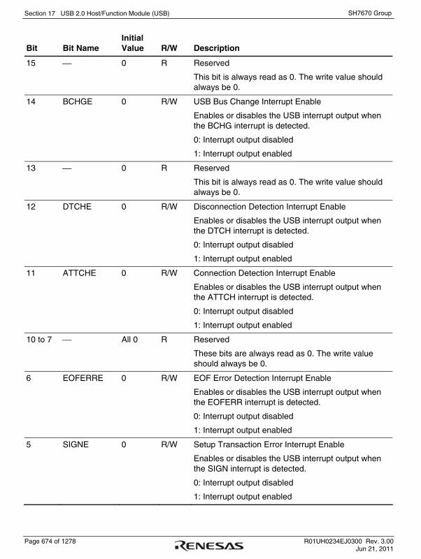
Section 17 USB 2.0 Host/Function Module (USB)
Page 674 of 1278 R01UH0234EJ0300 Rev. 3.00 Jun 21, 2011
SH7670 Group
Bit Bit Name Initial Value R/W Description
15 ⎯ 0 R Reserved
This bit is always read as 0. The write value should always be 0.
14 BCHGE 0 R/W USB Bus Change Interrupt Enable
Enables or disables the USB interrupt output when the BCHG interrupt is detected.
0: Interrupt output disabled
1: Interrupt output enabled
13 ⎯ 0 R Reserved
This bit is always read as 0. The write value should always be 0.
12 DTCHE 0 R/W Disconnection Detection Interrupt Enable
Enables or disables the USB interrupt output when the DTCH interrupt is detected.
0: Interrupt output disabled
1: Interrupt output enabled
11 ATTCHE 0 R/W Connection Detection Interrupt Enable
Enables or disables the USB interrupt output when the ATTCH interrupt is detected.
0: Interrupt output disabled
1: Interrupt output enabled
10 to 7 ⎯ All 0 R Reserved
These bits are always read as 0. The write value should always be 0.
6 EOFERRE 0 R/W EOF Error Detection Interrupt Enable
Enables or disables the USB interrupt output when the EOFERR interrupt is detected.
0: Interrupt output disabled
1: Interrupt output enabled
5 SIGNE 0 R/W Setup Transaction Error Interrupt Enable
Enables or disables the USB interrupt output when the SIGN interrupt is detected.
0: Interrupt output disabled
1: Interrupt output enabled

Section 17 USB 2.0 Host/Function Module (USB)
R01UH0234EJ0300 Rev. 3.00 Page 675 of 1278 Jun 21, 2011
SH7670 Group
Bit Bit Name Initial Value R/W Description
4 SACKE 0 R/W Setup Transaction Normal Response Interrupt Enable
Enables or disables the USB interrupt output when the SACK interrupt is detected.
0: Interrupt output disabled
1: Interrupt output enabled
3 to 0 ⎯ All 0 R Reserved
These bits are always read as 0. The write value should always be 0.
Note: The INTENB1 register bits can be set to 1 only when the host controller function is selected; do not set these bits to 1 to enable the corresponding interrupt output when the function controller function is selected.
17.3.12 BRDY Interrupt Enable Register (BRDYENB)
BRDYENB is a register that enables or disables the BRDY bit in INTSTS0 to be set to 1 when the BRDY interrupt is detected for each pipe.
On detecting the BRDY interrupt for the pipe corresponding to the bit in this register to which software has set 1, this module sets 1 to the corresponding PIPEBRDY bit in BRDYSTS and the BRDY bit in INTSTS0, and generates the BRDY interrupt.
While at least one PIPEBRDY bit in BRDYSTS indicates 1, this module generates the BRDY interrupt when software modifies the corresponding interrupt enable bit in BRDYENB from 0 to 1.
This register is initialized by a power-on reset.
15 14 13 12 11 10 9 8 7 6 5 4 3 2 1 0Bit:
Initial value:R/W:
0 0 0 0 0 0 0 0 0 0 0 0 0 0 0 0R R R R R R R/W R/W R/W R/W R/W R/W R/W R/W R/W R/W
— — — — — — PIPE9BRDYE
PIPE8BRDYE
PIPE7BRDYE
PIPE6BRDYE
PIPE5BRDYE
PIPE4BRDYE
PIPE3BRDYE
PIPE2BRDYE
PIPE1BRDYE
PIPE0BRDYE

Section 17 USB 2.0 Host/Function Module (USB)
Page 676 of 1278 R01UH0234EJ0300 Rev. 3.00 Jun 21, 2011
SH7670 Group
Bit Bit Name Initial Value R/W Description
15 to 10 ⎯ All 0 R Reserved
These bits are always read as 0. The write value should always be 0.
9 PIPE9BRDYE 0 R/W BRDY interrupt Enable for PIPE9
0: Interrupt output disabled
1: Interrupt output enabled
8 PIPE8BRDYE 0 R/W BRDY interrupt Enable for PIPE8
0: Interrupt output disabled
1: Interrupt output enabled
7 PIPE7BRDYE 0 R/W BRDY interrupt Enable for PIPE7
0: Interrupt output disabled
1: Interrupt output enabled
6 PIPE6BRDYE 0 R/W BRDY interrupt Enable for PIPE6
0: Interrupt output disabled
1: Interrupt output enabled
5 PIPE5BRDYE 0 R/W BRDY interrupt Enable for PIPE5
0: Interrupt output disabled
1: Interrupt output enabled
4 PIPE4BRDYE 0 R/W BRDY interrupt Enable for PIPE4
0: Interrupt output disabled
1: Interrupt output enabled
3 PIPE3BRDYE 0 R/W BRDY interrupt Enable for PIPE3
0: Interrupt output disabled
1: Interrupt output enabled
2 PIPE2BRDYE 0 R/W BRDY interrupt Enable for PIPE2
0: Interrupt output disabled
1: Interrupt output enabled
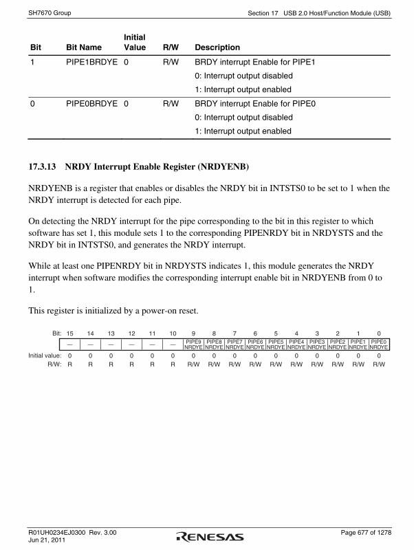
Section 17 USB 2.0 Host/Function Module (USB)
R01UH0234EJ0300 Rev. 3.00 Page 677 of 1278 Jun 21, 2011
SH7670 Group
Bit Bit Name Initial Value R/W Description
1 PIPE1BRDYE 0 R/W BRDY interrupt Enable for PIPE1
0: Interrupt output disabled
1: Interrupt output enabled
0 PIPE0BRDYE 0 R/W BRDY interrupt Enable for PIPE0
0: Interrupt output disabled
1: Interrupt output enabled
17.3.13 NRDY Interrupt Enable Register (NRDYENB)
NRDYENB is a register that enables or disables the NRDY bit in INTSTS0 to be set to 1 when the NRDY interrupt is detected for each pipe.
On detecting the NRDY interrupt for the pipe corresponding to the bit in this register to which software has set 1, this module sets 1 to the corresponding PIPENRDY bit in NRDYSTS and the NRDY bit in INTSTS0, and generates the NRDY interrupt.
While at least one PIPENRDY bit in NRDYSTS indicates 1, this module generates the NRDY interrupt when software modifies the corresponding interrupt enable bit in NRDYENB from 0 to 1.
This register is initialized by a power-on reset.
15 14 13 12 11 10 9 8 7 6 5 4 3 2 1 0Bit:
Initial value:R/W:
0 0 0 0 0 0 0 0 0 0 0 0 0 0 0 0R R R R R R R/W R/W R/W R/W R/W R/W R/W R/W R/W R/W
— — — — — — PIPE9NRDYE
PIPE8NRDYE
PIPE7NRDYE
PIPE6NRDYE
PIPE5NRDYE
PIPE4NRDYE
PIPE3NRDYE
PIPE2NRDYE
PIPE1NRDYE
PIPE0NRDYE

Section 17 USB 2.0 Host/Function Module (USB)
Page 678 of 1278 R01UH0234EJ0300 Rev. 3.00 Jun 21, 2011
SH7670 Group
Bit Bit Name Initial Value R/W Description
15 to 10 ⎯ All 0 R Reserved
These bits are always read as 0. The write value should always be 0.
9 PIPE9NRDYE 0 R/W NRDY Interrupt Enable for PIPE9
0: Interrupt output disabled
1: Interrupt output enabled
8 PIPE8NRDYE 0 R/W NRDY Interrupt Enable for PIPE8
0: Interrupt output disabled
1: Interrupt output enabled
7 PIPE7NRDYE 0 R/W NRDY Interrupt Enable for PIPE7
0: Interrupt output disabled
1: Interrupt output enabled
6 PIPE6NRDYE 0 R/W NRDY Interrupt Enable for PIPE6
0: Interrupt output disabled
1: Interrupt output enabled
5 PIPE5NRDYE 0 R/W NRDY Interrupt Enable for PIPE5
0: Interrupt output disabled
1: Interrupt output enabled
4 PIPE4NRDYE 0 R/W NRDY Interrupt Enable for PIPE4
0: Interrupt output disabled
1: Interrupt output enabled
3 PIPE3NRDYE 0 R/W NRDY Interrupt Enable for PIPE3
0: Interrupt output disabled
1: Interrupt output enabled
2 PIPE2NRDYE 0 R/W NRDY Interrupt Enable for PIPE2
0: Interrupt output disabled
1: Interrupt output enabled

Section 17 USB 2.0 Host/Function Module (USB)
R01UH0234EJ0300 Rev. 3.00 Page 679 of 1278 Jun 21, 2011
SH7670 Group
Bit Bit Name Initial Value R/W Description
1 PIPE1NRDYE 0 R/W NRDY Interrupt Enable for PIPE1
0: Interrupt output disabled
1: Interrupt output enabled
0 PIPE0NRDYE 0 R/W NRDY Interrupt Enable for PIPE0
0: Interrupt output disabled
1: Interrupt output enabled
17.3.14 BEMP Interrupt Enable Register (BEMPENB)
BEMPENB is a register that enables or disables the BEMP bit in INTSTS0 to be set to 1 when the BEMP interrupt is detected for each pipe.
On detecting the BEMP interrupt for the pipe corresponding to the bit in this register to which software has set 1, this module sets 1 to the corresponding PIPEBEMP bit in BEMPSTS and the BEMP bit in INTSTS0, and generates the BEMP interrupt.
While at least one PIPEBEMP bit in BEMPSTS indicates 1, this module generates the BEMP interrupt when software modifies the corresponding interrupt enable bit in BEMPENB from 0 to 1.
This register is initialized by a power-on reset.
15 14 13 12 11 10 9 8 7 6 5 4 3 2 1 0Bit:
Initial value:R/W:
0 0 0 0 0 0 0 0 0 0 0 0 0 0 0 0R R R R R R R/W R/W R/W R/W R/W R/W R/W R/W R/W R/W
— — — — — — PIPE9BEMPE
PIPE8BEMPE
PIPE7BEMPE
PIPE6BEMPE
PIPE5BEMPE
PIPE4BEMPE
PIPE3BEMPE
PIPE2BEMPE
PIPE1BEMPE
PIPE0BEMPE

Section 17 USB 2.0 Host/Function Module (USB)
Page 680 of 1278 R01UH0234EJ0300 Rev. 3.00 Jun 21, 2011
SH7670 Group
Bit Bit Name Initial Value R/W Description
15 to 10 ⎯ All 0 R Reserved
These bits are always read as 0. The write value should always be 0.
9 PIPE9BEMPE 0 R/W BEMP Interrupt Enable for PIPE9
0: Interrupt output disabled
1: Interrupt output enabled
8 PIPE8BEMPE 0 R/W BEMP Interrupt Enable for PIPE8
0: Interrupt output disabled
1: Interrupt output enabled
7 PIPE7BEMPE 0 R/W BEMP Interrupt Enable for PIPE7
0: Interrupt output disabled
1: Interrupt output enabled
6 PIPE6BEMPE 0 R/W BEMP Interrupt Enable for PIPE6
0: Interrupt output disabled
1: Interrupt output enabled
5 PIPE5BEMPE 0 R/W BEMP Interrupt Enable for PIPE5
0: Interrupt output disabled
1: Interrupt output enabled
4 PIPE4BEMPE 0 R/W BEMP Interrupt Enable for PIPE4
0: Interrupt output disabled
1: Interrupt output enabled
3 PIPE3BEMPE 0 R/W BEMP Interrupt Enable for PIPE3
0: Interrupt output disabled
1: Interrupt output enabled
2 PIPE2BEMPE 0 R/W BEMP Interrupt Enable for PIPE2
0: Interrupt output disabled
1: Interrupt output enabled
1 PIPE1BEMPE 0 R/W BEMP Interrupt Enable for PIPE1
0: Interrupt output disabled
1: Interrupt output enabled
0 PIPE0BEMPE 0 R/W BEMP Interrupt Enable for PIPE0
0: Interrupt output disabled
1: Interrupt output enabled

Section 17 USB 2.0 Host/Function Module (USB)
R01UH0234EJ0300 Rev. 3.00 Page 681 of 1278 Jun 21, 2011
SH7670 Group
17.3.15 SOF Control Register (SOFCFG)
SOFCFG is a register that specifies the transaction-enabled time and BRDY interrupt status clear timing.
This register is initialized by a power-on reset.
15 14 13 12 11 10 9 8 7 6 5 4 3 2 1 0Bit:
Initial value:R/W:
0 0 0 0 0 0 0 0 0 0 *0 0 0 0 0 0R R R R R R R R/W R R/W R RR RR R
— — — — — — — —TRNENSEL — —— —— —BRDYM
Bit Bit Name Initial Value R/W Description
15 to 9 ⎯ All 0 R Reserved
These bits are always read as 0. The write value should always be 0.
8 TRNENSEL 0 R/W Transaction-Enabled Time Select
Selects the transaction-enabled time either for full- or low-speed communication, where is the time in which this module issues tokens in a frame via the port.
0: For non-low-speed communication
1: For low-speed communication
This bit is valid only when the host controller function is selected. Even when the host controller function is selected, the setting of this bit has no effect on the transaction-enabled time during high-speed communication.
This bit should be set to 0 when the function controller function is selected.
7 ⎯ 0 R Reserved
This bit is always read as 0. The write value should always be 0.

Section 17 USB 2.0 Host/Function Module (USB)
Page 682 of 1278 R01UH0234EJ0300 Rev. 3.00 Jun 21, 2011
SH7670 Group
Bit Bit Name Initial Value R/W Description
6 BRDYM 0 R/W BRDY Interrupt Status Clear Timing for each Pipe
Specifies the timing for clearing the BRDY interrupt status for each pipe.
0: Software clears the status.
1: This module clears the status when data has been read from the FIFO buffer or data has been written to the FIFO buffer.
5 ⎯ 0* R Reserved
This bit is reserved. The previously read value should be written to this bit.
Note: Although this bit is initialized to 0 by a power-on reset, be sure to set this bit to 1 using the initialization routine of this module.
4 to 0 ⎯ All 0 R Reserved
These bits are always read as 0. The write value should always be 0.
Note: * Although this bit is initialized to 0 by a power-on reset, be sure to set this bit to 1 using the initialization routine of this module.

Section 17 USB 2.0 Host/Function Module (USB)
R01UH0234EJ0300 Rev. 3.00 Page 683 of 1278 Jun 21, 2011
SH7670 Group
17.3.16 Interrupt Status Register 0 (INTSTS0)
INTSTS0 is a register that indicates the status of the various interrupts detected.
This register is initialized by a power-on reset. By a USB bus reset, the DVSQ2 to DVSQ0 bits are initialized.
15 14 13 12 11 10 9 8 7 6 5 4 3 2 1 0Bit:
Initial value:R/W:
0 0 0 0 0 0 0 0 *3 *2 *2 *2 0 0 0 0R/W*7 R/W*7 R/W*7 R/W*7 R/W*7 R R R R R R R R/W*7 R R R
VBINT RESM SOFR DVST CTRT BEMP NRDY BRDY VBSTS DVSQ[2:0] VALID CTSQ[2:0]
Bit Bit Name Initial Value R/W Description
15 VBINT 0 R/W*7 VBUS Interrupt Status*4*5
0: VBUS interrupts not generated
1: VBUS interrupts generated
This module sets this bit to 1 on detecting a level change (high to low or low to high) in the VBUS pin input value. This module sets the VBSTS bit to indicate the VBUS pin input value. When the VBUS interrupt is generated, use software to repeat reading the VBSTS bit until the same value is read three or more times, and eliminate chattering.
14 RESM 0 R/W*7 Resume Interrupt Status*4*5*6
0: Resume interrupts not generated
1: Resume interrupts generated
When the function controller function is selected, this module sets this bit to 1 on detecting the falling edge of the signal on the DP pin in the suspended state (DVSQ = 1XX).
When the host controller function is selected, the read value is invalid.
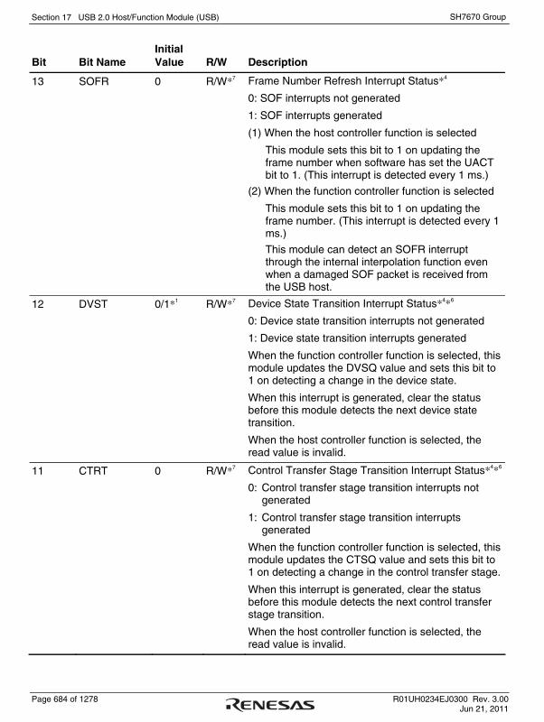
Section 17 USB 2.0 Host/Function Module (USB)
Page 684 of 1278 R01UH0234EJ0300 Rev. 3.00 Jun 21, 2011
SH7670 Group
Bit Bit Name Initial Value R/W Description
13 SOFR 0 R/W*7 Frame Number Refresh Interrupt Status*4
0: SOF interrupts not generated
1: SOF interrupts generated
(1) When the host controller function is selected
This module sets this bit to 1 on updating the frame number when software has set the UACT bit to 1. (This interrupt is detected every 1 ms.)
(2) When the function controller function is selected
This module sets this bit to 1 on updating the frame number. (This interrupt is detected every 1 ms.)
This module can detect an SOFR interrupt through the internal interpolation function even when a damaged SOF packet is received from the USB host.
12 DVST 0/1*1 R/W*7 Device State Transition Interrupt Status*4*6
0: Device state transition interrupts not generated
1: Device state transition interrupts generated
When the function controller function is selected, this module updates the DVSQ value and sets this bit to 1 on detecting a change in the device state.
When this interrupt is generated, clear the status before this module detects the next device state transition.
When the host controller function is selected, the read value is invalid.
11 CTRT 0 R/W*7 Control Transfer Stage Transition Interrupt Status*4*6
0: Control transfer stage transition interrupts not generated
1: Control transfer stage transition interrupts generated
When the function controller function is selected, this module updates the CTSQ value and sets this bit to 1 on detecting a change in the control transfer stage.
When this interrupt is generated, clear the status before this module detects the next control transfer stage transition.
When the host controller function is selected, the read value is invalid.
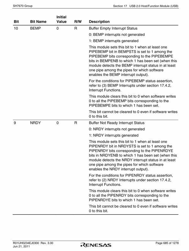
Section 17 USB 2.0 Host/Function Module (USB)
R01UH0234EJ0300 Rev. 3.00 Page 685 of 1278 Jun 21, 2011
SH7670 Group
Bit Bit Name Initial Value R/W Description
10 BEMP 0 R Buffer Empty Interrupt Status
0: BEMP interrupts not generated
1: BEMP interrupts generated
This module sets this bit to 1 when at least one PIPEBEMP bit in BEMPSTS is set to 1 among the PIPEBEMP bits corresponding to the PIPEBEMPE bits in BEMPENB to which 1 has been set (when this module detects the BEMP interrupt status in at least one pipe among the pipes for which software enables the BEMP interrupt output).
For the conditions for PIPEBEMP status assertion, refer to (3) BEMP Interrupts under section 17.4.2, Interrupt Functions.
This module clears this bit to 0 when software writes 0 to all the PIPEBEMP bits corresponding to the PIPEBEMPE bits to which 1 has been set.
This bit cannot be cleared to 0 even if software writes 0 to this bit.
9 NRDY 0 R Buffer Not Ready Interrupt Status
0: NRDY interrupts not generated
1: NRDY interrupts generated
This module sets this bit to 1 when at least one PIPENRDY bit in NRDYSTS is set to 1 among the PIPENRDY bits corresponding to the PIPENRDYE bits in NRDYENB to which 1 has been set (when this module detects the NRDY interrupt status in at least one pipe among the pipes for which software enables the NRDY interrupt output).
For the conditions for PIPENRDY status assertion, refer to (2) NRDY Interrupts under section 17.4.2, Interrupt Functions.
This module clears this bit to 0 when software writes 0 to all the PIPENRDY bits corresponding to the PIPENRDYE bits to which 1 has been set.
This bit cannot be cleared to 0 even if software writes 0 to this bit.

Section 17 USB 2.0 Host/Function Module (USB)
Page 686 of 1278 R01UH0234EJ0300 Rev. 3.00 Jun 21, 2011
SH7670 Group
Bit Bit Name Initial Value R/W Description
8 BRDY 0 R Buffer Ready Interrupt Status
Indicates the BRDY interrupt status.
0: BRDY interrupts not generated
1: BRDY interrupts generated
This module sets this bit to 1 when at least one PIPEBRDY bit in BRDYSTS is set to 1 among the PIPEBRDY bits corresponding to the PIPEBRDYE bits in BRDYENB to which 1 has been set (when this module detects the BRDY interrupt status in at least one pipe among the pipes for which software enables the BRDY interrupt output).
For the conditions for PIPEBRDY status assertion, refer to (1) BRDY Interrupts under section 17.4.2, Interrupt Functions.
This module clears this bit to 0 when software writes 0 to all the PIPEBRDY bits corresponding to the PIPEBRDYE bits to which 1 has been set.
This bit cannot be cleared to 0 even if software writes 0 to this bit.
7 VBSTS 0/1*3 R VBUS Input Status
0: The VBUS pin is low level.
1: The VBUS pin is high level.
6 to 4 DVSQ[2:0] 000/001*2 R Device State
000: Powered state
001: Default state
010: Address state
011: Configured state
1xx: Suspended state
When the host controller function is selected, the read value is invalid.

Section 17 USB 2.0 Host/Function Module (USB)
R01UH0234EJ0300 Rev. 3.00 Page 687 of 1278 Jun 21, 2011
SH7670 Group
Bit Bit Name Initial Value R/W Description
3 VALID 0 R/W*7 USB Request Reception
0: Not detected
1: Setup packet reception
When the host controller function is selected, the read value is invalid.
2 to 0 CTSQ[2:0] 000 R Control Transfer Stage
000: Idle or setup stage
001: Control read data stage
010: Control read status stage
011: Control write data stage
100: Control write status stage
101: Control write (no data) status stage
110: Control transfer sequence error
111: Setting prohibited
When the host controller function is selected, the read value is invalid.
Notes: 1. This bit is initialized to B'0 by a power-on reset and B'1 by a USB bus reset. 2. These bits are initialized to B'000 by a power-on reset and B'001 by a USB bus reset.
3. This bit is initialized to 0 when the level of the VBUS pin input is high and 1 when low.
4. To clear the VBINT, RESM, SOFR, DVST, or CTRT bit, write 0 only to the bits to be cleared; write 1 to the other bits. Do not write 0 to the status bits indicating 0.
5. A change in the status indicated by the VBINT and RESM bits can be detected even while the clock supply is stopped (while SCKE is 0), and the interrupts are output when the corresponding interrupt enable bits are enabled. Clearing the status through software should be done after enabling the clock supply.
6. A change in the status of the RESM, DVST, and CTRT bits occur only when the function controller function is selected; disable the corresponding interrupt enable bits (set to 0) when the function controller function is selected.
7. Only 0 can be written to.
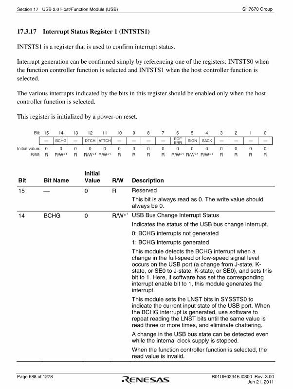
Section 17 USB 2.0 Host/Function Module (USB)
Page 688 of 1278 R01UH0234EJ0300 Rev. 3.00 Jun 21, 2011
SH7670 Group
17.3.17 Interrupt Status Register 1 (INTSTS1)
INTSTS1 is a register that is used to confirm interrupt status.
Interrupt generation can be confirmed simply by referencing one of the registers: INTSTS0 when the function controller function is selected and INTSTS1 when the host controller function is selected.
The various interrupts indicated by the bits in this register should be enabled only when the host controller function is selected.
This register is initialized by a power-on reset.
15 14 13 12 11 10 9 8 7 6 5 4 3 2 1 0Bit:
Initial value:R/W:
0 0 0 0 0 0 0 0 0 0 0 0 0 0 0 0R R/W*1 R R/W*1 R/W*1 R R R R R/W*1 R/W*1 R/W*1 R R R R
— BCHG — DTCH ATTCH — — — — EOFERR SIGN SACK — — — —
Bit Bit Name Initial Value R/W Description
15 ⎯ 0 R Reserved
This bit is always read as 0. The write value should always be 0.
14 BCHG 0 R/W*1 USB Bus Change Interrupt Status
Indicates the status of the USB bus change interrupt.
0: BCHG interrupts not generated
1: BCHG interrupts generated
This module detects the BCHG interrupt when a change in the full-speed or low-speed signal level occurs on the USB port (a change from J-state, K-state, or SE0 to J-state, K-state, or SE0), and sets this bit to 1. Here, if software has set the corresponding interrupt enable bit to 1, this module generates the interrupt.
This module sets the LNST bits in SYSSTS0 to indicate the current input state of the USB port. When the BCHG interrupt is generated, use software to repeat reading the LNST bits until the same value is read three or more times, and eliminate chattering.
A change in the USB bus state can be detected even while the internal clock supply is stopped.
When the function controller function is selected, the read value is invalid.
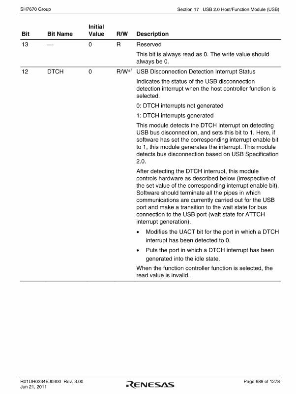
Section 17 USB 2.0 Host/Function Module (USB)
R01UH0234EJ0300 Rev. 3.00 Page 689 of 1278 Jun 21, 2011
SH7670 Group
Bit Bit Name Initial Value R/W Description
13 ⎯ 0 R Reserved
This bit is always read as 0. The write value should always be 0.
12 DTCH 0 R/W*1 USB Disconnection Detection Interrupt Status
Indicates the status of the USB disconnection detection interrupt when the host controller function is selected.
0: DTCH interrupts not generated
1: DTCH interrupts generated
This module detects the DTCH interrupt on detecting USB bus disconnection, and sets this bit to 1. Here, if software has set the corresponding interrupt enable bit to 1, this module generates the interrupt. This module detects bus disconnection based on USB Specification 2.0.
After detecting the DTCH interrupt, this module controls hardware as described below (irrespective of the set value of the corresponding interrupt enable bit). Software should terminate all the pipes in which communications are currently carried out for the USB port and make a transition to the wait state for bus connection to the USB port (wait state for ATTCH interrupt generation).
• Modifies the UACT bit for the port in which a DTCH
interrupt has been detected to 0.
• Puts the port in which a DTCH interrupt has been
generated into the idle state.
When the function controller function is selected, the read value is invalid.

Section 17 USB 2.0 Host/Function Module (USB)
Page 690 of 1278 R01UH0234EJ0300 Rev. 3.00 Jun 21, 2011
SH7670 Group
Bit Bit Name Initial Value R/W Description
11 ATTCH 0 R/W*1 ATTCH Interrupt Status
Indicates the status of the ATTCH interrupt when the host controller function is selected.
0: ATTCH interrupts not generated
1: ATTCH interrupts generated
This module detects the ATTCH interrupt on detecting J-state or K-state of the full-speed or low-speed level signal for 2.5 μs, and sets this bit to 1. Here, if software has set the corresponding interrupt enable bit to 1, this module generates the interrupt.
Specifically, this module detects the ATTCH interrupt on any of the following conditions.
• K-state, SE0, or SE1 changes to J-state, and J-
state continues 2.5 μs.
• J-state, SE0, or SE1 changes to K-state, and K-
state continues 2.5 μs.
When the function controller function is selected, the read value is invalid.
10 to 7 ⎯ All 0 R Reserved
These bits are always read as 0. The write value should always be 0.
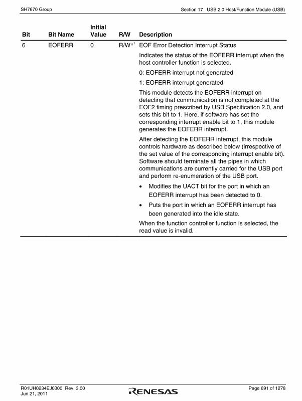
Section 17 USB 2.0 Host/Function Module (USB)
R01UH0234EJ0300 Rev. 3.00 Page 691 of 1278 Jun 21, 2011
SH7670 Group
Bit Bit Name Initial Value R/W Description
6 EOFERR 0 R/W*1 EOF Error Detection Interrupt Status
Indicates the status of the EOFERR interrupt when the host controller function is selected.
0: EOFERR interrupt not generated
1: EOFERR interrupt generated
This module detects the EOFERR interrupt on detecting that communication is not completed at the EOF2 timing prescribed by USB Specification 2.0, and sets this bit to 1. Here, if software has set the corresponding interrupt enable bit to 1, this module generates the EOFERR interrupt.
After detecting the EOFERR interrupt, this module controls hardware as described below (irrespective of the set value of the corresponding interrupt enable bit). Software should terminate all the pipes in which communications are currently carried for the USB port and perform re-enumeration of the USB port.
• Modifies the UACT bit for the port in which an
EOFERR interrupt has been detected to 0.
• Puts the port in which an EOFERR interrupt has
been generated into the idle state.
When the function controller function is selected, the read value is invalid.

Section 17 USB 2.0 Host/Function Module (USB)
Page 692 of 1278 R01UH0234EJ0300 Rev. 3.00 Jun 21, 2011
SH7670 Group
Bit Bit Name Initial Value R/W Description
5 SIGN 0 R/W*1 Setup Transaction Error Interrupt Status
Indicates the status of the setup transaction error interrupt when the host controller function is selected.
0: SIGN interrupts not generated
1: SIGN interrupts generated
This module detects the SIGN interrupt when ACK response is not returned from the peripheral device three consecutive times during the setup transactions issued by this module, and sets this bit to 1. Here, if software has set the corresponding interrupt enable bit to 1, this module generates the SIGN interrupt.
Specifically, this module detects the SIGN interrupt when any of the following response conditions occur for three consecutive setup transactions.
• Timeout is detected when the peripheral device
has returned no response.
• A damaged ACK packet is received.
• A handshake other than ACK (NAK, NYET, or
STALL) is received.
When the function controller function is selected, the read value is invalid.
4 SACK 0 R/W*1 Setup Transaction Normal Response Interrupt Status
Indicates the status of the setup transaction normal response interrupt when the host controller function is selected.
0: SACK interrupts not generated
1: SACK interrupts generated
This module detects the SACK interrupt when ACK response is returned from the peripheral device during the setup transactions issued by this module, and sets this bit to 1. Here, if software has set the corresponding interrupt enable bit to 1, this module generates the SACK interrupt.

Section 17 USB 2.0 Host/Function Module (USB)
R01UH0234EJ0300 Rev. 3.00 Page 693 of 1278 Jun 21, 2011
SH7670 Group
Bit Bit Name Initial Value R/W Description
3 to 0 ⎯ All 0 R Reserved
These bits are always read as 0. The write value should always be 0.
Notes: 1. To clear the status indicated by the bits in this register, write 0 only to the bits to be cleared; write 1 to the other bits.
2. A change in the status indicated by the BCHG bit can be detected even while the clock supply is stopped (while SCKE is 0), and the interrupt is output when the corresponding interrupt enable bit is enabled. Clearing the status through software should be done after enabling the clock supply. No interrupts other than BCHG can be detected while the clock supply is stopped (while SCKE is 0).

Section 17 USB 2.0 Host/Function Module (USB)
Page 694 of 1278 R01UH0234EJ0300 Rev. 3.00 Jun 21, 2011
SH7670 Group
17.3.18 BRDY Interrupt Status Register (BRDYSTS)
BRDYSTS is a register that indicates the BRDY interrupt status for each pipe.
This register is initialized by a power-on reset.
15 14 13 12 11 10 9 8 7 6 5 4 3 2 1 0Bit:
Initial value:R/W:
0 0 0 0 0 0 0 0 0 0 0 0 0 0 0 0R R R R R R R/W*1 R/W*1 R/W*1 R/W*1 R/W*1 R/W*1 R/W*1 R/W*1 R/W*1 R/W*1
— — — — — — PIPE9BRDY
PIPE8BRDY
PIPE7BRDY
PIPE6BRDY
PIPE5BRDY
PIPE4BRDY
PIPE3BRDY
PIPE2BRDY
PIPE1BRDY
PIPE0BRDY
Bit Bit Name Initial Value R/W Description
15 to 10 ⎯ All 0 R Reserved
These bits are always read as 0. The write value should always be 0.
9 PIPE9BRDY 0 R/W*1 BRDY Interrupt Status for PIPE9*2
0: Interrupts not generated
1: Interrupts generated
8 PIPE8BRDY 0 R/W*1 BRDY Interrupt Status for PIPE8*2
0: Interrupts not generated
1: Interrupts generated
7 PIPE7BRDY 0 R/W*1 BRDY Interrupt Status for PIPE7*2
0: Interrupts not generated
1: Interrupts generated
6 PIPE6BRDY 0 R/W*1 BRDY Interrupt Status for PIPE6*2
0: Interrupts not generated
1: Interrupts generated
5 PIPE5BRDY 0 R/W*1 BRDY Interrupt Status for PIPE5*2
0: Interrupts not generated
1: Interrupts generated
4 PIPE4BRDY 0 R/W*1 BRDY Interrupt Status for PIPE4*2
0: Interrupts not generated
1: Interrupts generated
3 PIPE3BRDY 0 R/W*1 BRDY Interrupt Status for PIPE3*2
0: Interrupts not generated
1: Interrupts generated
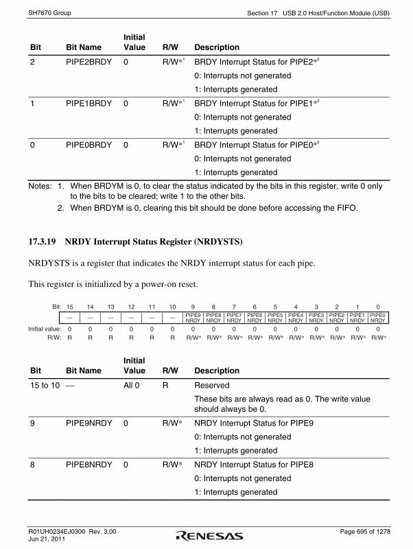
Section 17 USB 2.0 Host/Function Module (USB)
R01UH0234EJ0300 Rev. 3.00 Page 695 of 1278 Jun 21, 2011
SH7670 Group
Bit Bit Name Initial Value R/W Description
2 PIPE2BRDY 0 R/W*1 BRDY Interrupt Status for PIPE2*2
0: Interrupts not generated
1: Interrupts generated
1 PIPE1BRDY 0 R/W*1 BRDY Interrupt Status for PIPE1*2
0: Interrupts not generated
1: Interrupts generated
0 PIPE0BRDY 0 R/W*1 BRDY Interrupt Status for PIPE0*2
0: Interrupts not generated
1: Interrupts generated
Notes: 1. When BRDYM is 0, to clear the status indicated by the bits in this register, write 0 only to the bits to be cleared; write 1 to the other bits.
2. When BRDYM is 0, clearing this bit should be done before accessing the FIFO.
17.3.19 NRDY Interrupt Status Register (NRDYSTS)
NRDYSTS is a register that indicates the NRDY interrupt status for each pipe.
This register is initialized by a power-on reset.
15 14 13 12 11 10 9 8 7 6 5 4 3 2 1 0Bit:
Initial value:R/W:
0 0 0 0 0 0 0 0 0 0 0 0 0 0 0 0R R R R R R R/W* R/W* R/W* R/W* R/W* R/W* R/W* R/W* R/W* R/W*
— — — — — — PIPE9NRDY
PIPE8NRDY
PIPE7NRDY
PIPE6NRDY
PIPE5NRDY
PIPE4NRDY
PIPE3NRDY
PIPE2NRDY
PIPE1NRDY
PIPE0NRDY
Bit Bit Name Initial Value R/W Description
15 to 10 ⎯ All 0 R Reserved
These bits are always read as 0. The write value should always be 0.
9 PIPE9NRDY 0 R/W* NRDY Interrupt Status for PIPE9
0: Interrupts not generated
1: Interrupts generated
8 PIPE8NRDY 0 R/W* NRDY Interrupt Status for PIPE8
0: Interrupts not generated
1: Interrupts generated
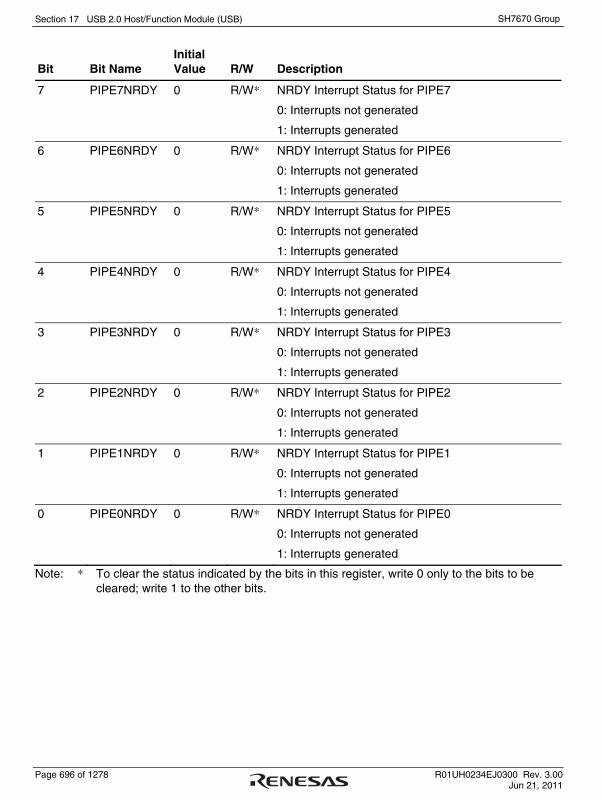
Section 17 USB 2.0 Host/Function Module (USB)
Page 696 of 1278 R01UH0234EJ0300 Rev. 3.00 Jun 21, 2011
SH7670 Group
Bit Bit Name Initial Value R/W Description
7 PIPE7NRDY 0 R/W* NRDY Interrupt Status for PIPE7
0: Interrupts not generated
1: Interrupts generated
6 PIPE6NRDY 0 R/W* NRDY Interrupt Status for PIPE6
0: Interrupts not generated
1: Interrupts generated
5 PIPE5NRDY 0 R/W* NRDY Interrupt Status for PIPE5
0: Interrupts not generated
1: Interrupts generated
4 PIPE4NRDY 0 R/W* NRDY Interrupt Status for PIPE4
0: Interrupts not generated
1: Interrupts generated
3 PIPE3NRDY 0 R/W* NRDY Interrupt Status for PIPE3
0: Interrupts not generated
1: Interrupts generated
2 PIPE2NRDY 0 R/W* NRDY Interrupt Status for PIPE2
0: Interrupts not generated
1: Interrupts generated
1 PIPE1NRDY 0 R/W* NRDY Interrupt Status for PIPE1
0: Interrupts not generated
1: Interrupts generated
0 PIPE0NRDY 0 R/W* NRDY Interrupt Status for PIPE0
0: Interrupts not generated
1: Interrupts generated
Note: * To clear the status indicated by the bits in this register, write 0 only to the bits to be cleared; write 1 to the other bits.

Section 17 USB 2.0 Host/Function Module (USB)
R01UH0234EJ0300 Rev. 3.00 Page 697 of 1278 Jun 21, 2011
SH7670 Group
17.3.20 BEMP Interrupt Status Register (BEMPSTS)
BEMPSTS is a register that indicates the BEMP interrupt status for each pipe.
This register is initialized by a power-on reset.
15 14 13 12 11 10 9 8 7 6 5 4 3 2 1 0Bit:
Initial value:R/W:
0 0 0 0 0 0 0 0 0 0 0 0 0 0 0 0R R R R R R R/W* R/W* R/W* R/W* R/W* R/W* R/W* R/W* R/W* R/W*
— — — — — — PIPE9BEMP
PIPE8BEMP
PIPE7BEMP
PIPE6BEMP
PIPE5BEMP
PIPE4BEMP
PIPE3BEMP
PIPE2BEMP
PIPE1BEMP
PIPE0BEMP
Bit Bit Name Initial Value R/W Description
15 to 10 ⎯ All 0 R Reserved
These bits are always read as 0. The write value should always be 0.
9 PIPE9BEMP 0 R/W* BEMP Interrupts for PIPE9
0: Interrupts not generated
1: Interrupts generated
8 PIPE8BEMP 0 R/W* BEMP Interrupts for PIPE8
0: Interrupts not generated
1: Interrupts generated
7 PIPE7BEMP 0 R/W* BEMP Interrupts for PIPE7
0: Interrupts not generated
1: Interrupts generated
6 PIPE6BEMP 0 R/W* BEMP Interrupts for PIPE6
0: Interrupts not generated
1: Interrupts generated

Section 17 USB 2.0 Host/Function Module (USB)
Page 698 of 1278 R01UH0234EJ0300 Rev. 3.00 Jun 21, 2011
SH7670 Group
Bit Bit Name Initial Value R/W Description
5 PIPE5BEMP 0 R/W* BEMP Interrupts for PIPE5
0: Interrupts not generated
1: Interrupts generated
4 PIPE4BEMP 0 R/W* BEMP Interrupts for PIPE4
0: Interrupts not generated
1: Interrupts generated
3 PIPE3BEMP 0 R/W* BEMP Interrupts for PIPE3
0: Interrupts not generated
1: Interrupts generated
2 PIPE2BEMP 0 R/W* BEMP Interrupts for PIPE2
0: Interrupts not generated
1: Interrupts generated
1 PIPE1BEMP 0 R/W* BEMP Interrupts for PIPE1
0: Interrupts not generated
1: Interrupts generated
0 PIPE0BEMP 0 R/W* BEMP Interrupts for PIPE0
0: Interrupts not generated
1: Interrupts generated
Note: * To clear the status indicated by the bits in this register, write 0 only to the bits to be cleared; write 1 to the other bits.
17.3.21 Frame Number Register (FRMNUM)
FRMNUM is a register that determines the source of isochronous error notification and indicates the frame number.
This register is initialized by a power-on reset.
15 14 13 12 11 10 9 8 7 6 5 4 3 2 1 0Bit:
Initial value:R/W:
0 0 0 0 0 0 0 0 0 0 0 0 0 0 0 0R/W* R/W* R R R R R R R R R R R R R R
OVRN CRCE — — — FRNM[10:0]

Section 17 USB 2.0 Host/Function Module (USB)
R01UH0234EJ0300 Rev. 3.00 Page 699 of 1278 Jun 21, 2011
SH7670 Group
Bit Bit Name Initial Value R/W Description
15 OVRN 0 R/W* Overrun/Underrun Detection Status
Indicates whether an overrun/underrun error has been detected in the pipe during isochronous transfer.
0: No error
1: An error occurred
Software can clear this bit to 0 by writing 0 to the bit. Here, 1 should be written to the other bits in this register.
(1) When the host controller function is selected
This module sets this bit to 1 on any of the following conditions.
• For the isochronous transfer pipe in the
transmitting direction, the time to issue an OUT
token comes before all the transmit data has
been written to the FIFO buffer.
• For the isochronous transfer pipe in the receiving
direction, the time to issue an IN token comes
when no FIFO buffer planes are empty.
(2) When the function controller function is selected
This module sets this bit to 1 on any of the following conditions.
• For the isochronous transfer pipe in the
transmitting direction, the IN token is received
before all the transmit data has been written to
the FIFO buffer.
• For the isochronous transfer pipe in the receiving
direction, the OUT token is received when no
FIFO buffer planes are empty.

Section 17 USB 2.0 Host/Function Module (USB)
Page 700 of 1278 R01UH0234EJ0300 Rev. 3.00 Jun 21, 2011
SH7670 Group
Bit Bit Name Initial Value R/W Description
14 CRCE 0 R/W* Receive Data Error
Indicates whether a CRC error or bit stuffing error has been detected in the pipe during isochronous transfer.
0: No error
1: An error occurred
Software can clear this bit to 0 by writing 0 to the bit. Here, 1 should be written to the other bits in this register.
(1) When the host controller function is selected
On detecting a CRC error, this module generates the internal NRDY interrupt request.
(2) When the function controller function is selected
On detecting a CRC error, this module does not generate the internal NRDY interrupt request.
13 to 11 ⎯ All 0 R Reserved
These bits are always read as 0. The write value should always be 0.
10 to 0 FRNM[10:0] H'000 R Frame Number
This module sets these bits to indicate the latest frame number, which is updated every time an SOF packet is issued or received (every 1 ms)
Repeat reading these bits until the same value is read twice.
Note: * Only 0 can be written to
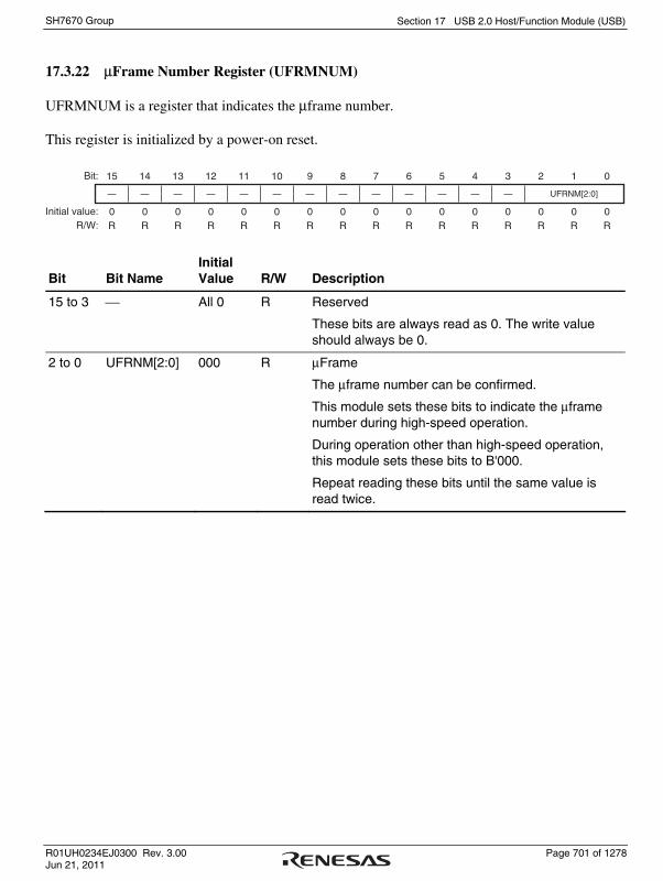
Section 17 USB 2.0 Host/Function Module (USB)
R01UH0234EJ0300 Rev. 3.00 Page 701 of 1278 Jun 21, 2011
SH7670 Group
17.3.22 μFrame Number Register (UFRMNUM)
UFRMNUM is a register that indicates the μframe number.
This register is initialized by a power-on reset.
15 14 13 12 11 10 9 8 7 6 5 4 3 2 1 0Bit:
Initial value:R/W:
0 0 0 0 0 0 0 0 0 0 0 0 0 0 0 0R R R R R R R R R R R R R R R R
— — — — — — — — — — — — — UFRNM[2:0]
Bit Bit Name Initial Value R/W Description
15 to 3 ⎯ All 0 R Reserved
These bits are always read as 0. The write value should always be 0.
2 to 0 UFRNM[2:0] 000 R μFrame
The μframe number can be confirmed.
This module sets these bits to indicate the μframe number during high-speed operation.
During operation other than high-speed operation, this module sets these bits to B'000.
Repeat reading these bits until the same value is read twice.

Section 17 USB 2.0 Host/Function Module (USB)
Page 702 of 1278 R01UH0234EJ0300 Rev. 3.00 Jun 21, 2011
SH7670 Group
17.3.23 USB Address Register (USBADDR)
USBADDR is a register that indicates the USB address. This register is valid only when the function controller function is selected. When the host controller function is selected, peripheral device addresses should be set using the DEVSEL bits in PIPEMAXP.
This register is initialized by a power-on reset or a USB bus reset.
15 14 13 12 11 10 9 8 7 6 5 4 3 2 1 0Bit:
Initial value:R/W:
0 0 0 0 0 0 0 0 0 0 0 0 0 0 0 0R R R R R R R R R R R R R R R R
— — — — — — — — — USBADDR[6:0]
Bit Bit Name Initial Value R/W Description
15 to 7 ⎯ All 0 R Reserved
These bits are always read as 0. The write value should always be 0.
6 to 0 USBADDR [6:0]
H'00 R USB Address
When the function controller function is selected, these bits indicate the USB address assigned by the host when the SET_ADDRESS request is successfully processed.
On detecting the USB reset, this module sets these bits to H'00.
When the host controller function is selected, these bits are invalid.
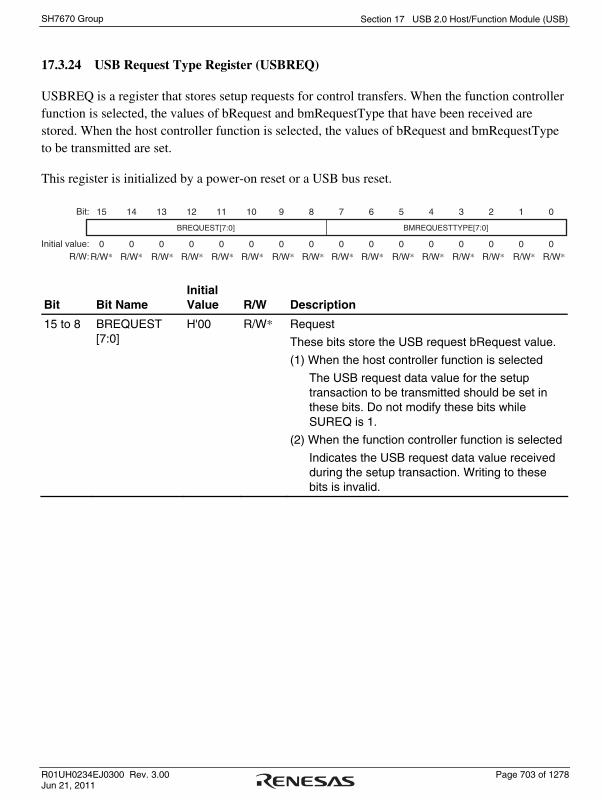
Section 17 USB 2.0 Host/Function Module (USB)
R01UH0234EJ0300 Rev. 3.00 Page 703 of 1278 Jun 21, 2011
SH7670 Group
17.3.24 USB Request Type Register (USBREQ)
USBREQ is a register that stores setup requests for control transfers. When the function controller function is selected, the values of bRequest and bmRequestType that have been received are stored. When the host controller function is selected, the values of bRequest and bmRequestType to be transmitted are set.
This register is initialized by a power-on reset or a USB bus reset.
15 14 13 12 11 10 9 8 7 6 5 4 3 2 1 0Bit:
Initial value:R/W:
0 0 0 0 0 0 0 0 0 0 0 0 0 0 0 0R/W* R/W* R/W* R/W* R/W* R/W* R/W* R/W* R/W* R/W* R/W* R/W* R/W* R/W* R/W* R/W*
BREQUEST[7:0] BMREQUESTTYPE[7:0]
Bit Bit Name Initial Value R/W Description
15 to 8 BREQUEST [7:0]
H'00 R/W* Request
These bits store the USB request bRequest value.
(1) When the host controller function is selected
The USB request data value for the setup transaction to be transmitted should be set in these bits. Do not modify these bits while SUREQ is 1.
(2) When the function controller function is selected
Indicates the USB request data value received during the setup transaction. Writing to these bits is invalid.
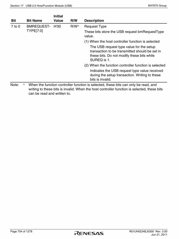
Section 17 USB 2.0 Host/Function Module (USB)
Page 704 of 1278 R01UH0234EJ0300 Rev. 3.00 Jun 21, 2011
SH7670 Group
Bit Bit Name Initial Value R/W Description
7 to 0 BMREQUEST-TYPE[7:0]
H'00 R/W* Request Type
These bits store the USB request bmRequestType value.
(1) When the host controller function is selected
The USB request type value for the setup transaction to be transmitted should be set in these bits. Do not modify these bits while SUREQ is 1.
(2) When the function controller function is selected
Indicates the USB request type value received during the setup transaction. Writing to these bits is invalid.
Note: * When the function controller function is selected, these bits can only be read, and writing to these bits is invalid. When the host controller function is selected, these bits can be read and written to.

Section 17 USB 2.0 Host/Function Module (USB)
R01UH0234EJ0300 Rev. 3.00 Page 705 of 1278 Jun 21, 2011
SH7670 Group
17.3.25 USB Request Value Register (USBVAL)
USBVAL is a register that stores setup requests for control transfers. When the function controller function is selected, the value of wValue that has been received is stored. When the host controller function is selected, the value of wValue to be transmitted is set.
This register is initialized by a power-on reset or a USB bus reset.
15 14 13 12 11 10 9 8 7 6 5 4 3 2 1 0Bit:
Initial value:R/W:
0 0 0 0 0 0 0 0 0 0 0 0 0 0 0 0
WVALUE[15:0]
R/W* R/W* R/W* R/W* R/W* R/W* R/W* R/W* R/W* R/W* R/W* R/W* R/W* R/W* R/W* R/W*
Bit Bit Name Initial Value R/W Description
15 to 0 WValue[15:0] H'0000 R/W* Value
These bits store the USB request wValue value.
(1) When the host controller function is selected
The USB request wValue value for the setup transaction to be transmitted should be set in these bits. Do not modify these bits while SUREQ is 1.
(2) When the function controller function is selected
Indicates the USB request wValue value received during the setup transaction. Writing to these bits is invalid.
Note: * When the function controller function is selected, these bits can only be read, and writing to these bits is invalid. When the host controller function is selected, these bits can be read and written to.

Section 17 USB 2.0 Host/Function Module (USB)
Page 706 of 1278 R01UH0234EJ0300 Rev. 3.00 Jun 21, 2011
SH7670 Group
17.3.26 USB Request Index Register (USBINDX)
USBINDEX is a register that stores setup requests for control transfers. When the function controller function is selected, the value of wIndex that has been received is stored. When the host controller function is selected, the value of wIndex to be transmitted is set.
This register is initialized by a power-on reset or a USB bus reset.
15 14 13 12 11 10 9 8 7 6 5 4 3 2 1 0Bit:
Initial value:R/W:
0 0 0 0 0 0 0 0 0 0 0 0 0 0 0 0
WINDEX[15:0]
R/W* R/W* R/W* R/W* R/W* R/W* R/W* R/W* R/W* R/W* R/W* R/W* R/W* R/W* R/W* R/W*
Bit Bit Name Initial Value R/W Description
15 to 0 WINDEX[15:0] H'0000 R/W* Index
These bits store the USB request wIndex value.
(1) When the host controller function is selected
The USB request wIndex value for the setup transaction to be transmitted should be set in these bits. Do not modify these bits while SUREQ is 1.
(2) When the function controller function is selected
Indicates the USB request wIndex value received during the setup transaction. Writing to these bits is invalid.
Note: * When the function controller function is selected, these bits can only be read, and writing to these bits is invalid. When the host controller function is selected, these bits can be read and written to.
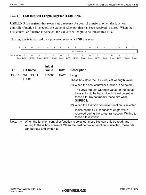
Section 17 USB 2.0 Host/Function Module (USB)
R01UH0234EJ0300 Rev. 3.00 Page 707 of 1278 Jun 21, 2011
SH7670 Group
17.3.27 USB Request Length Register (USBLENG)
USBLENG is a register that stores setup requests for control transfers. When the function controller function is selected, the value of wLength that has been received is stored. When the host controller function is selected, the value of wLength to be transmitted is set.
This register is initialized by a power-on reset or a USB bus reset.
15 14 13 12 11 10 9 8 7 6 5 4 3 2 1 0Bit:
Initial value:R/W:
0 0 0 0 0 0 0 0 0 0 0 0 0 0 0 0R/W* R/W* R/W* R/W* R/W* R/W* R/W* R/W* R/W* R/W* R/W* R/W* R/W* R/W* R/W* R/W*
WLENGTH[15:0]
Bit Bit Name Initial Value R/W Description
15 to 0 WLENGTH [15:0]
H'0000 R/W* Length
These bits store the USB request wLength value.
(1) When the host controller function is selected
The USB request wLength value for the setup transaction to be transmitted should be set in these bits. Do not modify these bits while SUREQ is 1.
(2) When the function controller function is selected
Indicates the USB request wLength value received during the setup transaction. Writing to these bits is invalid.
Note: * When the function controller function is selected, these bits can only be read, and writing to these bits is invalid. When the host controller function is selected, these bits can be read and written to.

Section 17 USB 2.0 Host/Function Module (USB)
Page 708 of 1278 R01UH0234EJ0300 Rev. 3.00 Jun 21, 2011
SH7670 Group
17.3.28 DCP Configuration Register (DCPCFG)
DCPCFG is a register that specifies the data transfer direction for the default control pipe (DCP).
This register is initialized by a power-on reset.
15 14 13 12 11 10 9 8 7 6 5 4 3 2 1 0Bit:
Initial value:R/W:
0 0 0 0 0 0 0 0 0 0 0 0 0 0 0 0R R R R R R R R R R R R/W R R R R
— — — — — — — — — — — DIR — — — —
Bit Bit Name Initial Value R/W Description
15 to 5 ⎯ All 0 R Reserved
These bits are always read as 0. The write value should always be 0.
4 DIR 0 R/W Transfer Direction
When the host controller function is selected, this bit sets the transfer direction of data stage.
0: Data receiving direction
1: Data transmitting direction
When the function controller function is selected, this bit should be cleared to 0.
3 to 0 ⎯ All 0 R Reserved
These bits are always read as 0. The write value should always be 0.

Section 17 USB 2.0 Host/Function Module (USB)
R01UH0234EJ0300 Rev. 3.00 Page 709 of 1278 Jun 21, 2011
SH7670 Group
17.3.29 DCP Maximum Packet Size Register (DCPMAXP)
DCPMAXP is a register that specifies the maximum packet size for the DCP.
This register is initialized by a power-on reset.
15 14 13 12 11 10 9 8 7 6 5 4 3 2 1 0Bit:
Initial value:R/W:
0 0 0 0 0 0 0 0 0 0 1 0 0 0 0 0R/W R/W R/W R/W R R R R R R/W R/W R/W R/W R R R
— — — — — MXPS[6:0]DEVSEL[3:0]
Bit Bit Name Initial Value R/W Description
15 to 12 DEVSEL[3:0] 0000 R/W Device Select
When the host controller function is selected, these bits specify the communication target peripheral device address.
0000: Address 0000
0001: Address 0001
: :
1001: Address 1001
1010: Address 1010
Other than above: Setting prohibited
These bits should be set after setting the address to the DEVADDn register corresponding to the value to be set in these bits.
For example, before setting DEVSEL to 0010, the address should be set to the DEVADD2 register.
These bits should be set while CSSTS is 0, PID is NAK, and SUREQ is 0.
Before modifying these bits after modifying the PID bits for the DCP from BUF to NAK, check that CSSTS and PBUSY are 0. However, if the PID bits have been modified to NAK by this module, checking PBUSY through software is not necessary.
When the function controller function is selected, these bits should be set to B'0000.

Section 17 USB 2.0 Host/Function Module (USB)
Page 710 of 1278 R01UH0234EJ0300 Rev. 3.00 Jun 21, 2011
SH7670 Group
Bit Bit Name Initial Value R/W Description
11 to 7 ⎯ All 0 R Reserved
These bits are always read as 0. The write value should always be 0.
6 to 0 MXPS[6:0] H'40 R/W Maximum Packet Size
Specifies the maximum data payload (maximum packet size) for the DCP.
These bits are initialized to H'40 (64 bytes).
These bits should be set to the value based on the USB Specification.
These bits should be set while CSSTS is 0 and PID is NAK and before the pipe is selected by the CURPIPE bits.
Before modifying these bits after modifying the PID bits for the corresponding pipe from BUF to NAK, check that CSSTS and PBUSY are 0. However, if the PID bits have been modified to NAK by this module, checking PBUSY through software is not necessary.
While MXPS is 0, do not write to the FIFO buffer or do not set PID to BUF.
17.3.30 DCP Control Register (DCPCTR)
DCPCTR is a register that is used to confirm the buffer memory status, change and confirm the data PID sequence bit, and set the response PID for the DCP.
This register is initialized by a power-on reset. The CCPL and PID[1:0] bits are initialized by a USB bus reset.
15 14 13 12 11 10 9 8 7 6 5 4 3 2 1 0Bit:
Initial value:R/W:
0 0 0 0 0 0 0 0 0 1 0 0 0 0 0 0R R/W*1 R/W R/W*1 R R R/W*1R/W*2 R/W*1 R R R/W R R/W*1 R/W R/W
BSTS SUREQ CSCLR CSSTS SUREQCLR — — SQCLR SQSET SQMON PBUSY PINGE — CCPL PID[1:0]
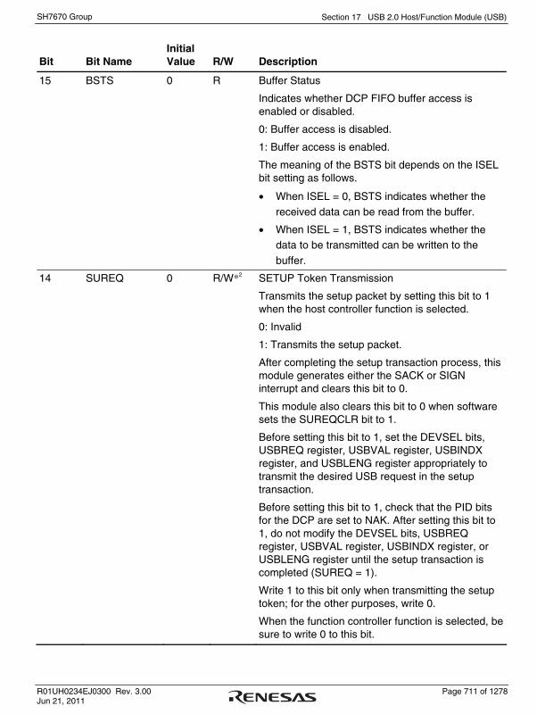
Section 17 USB 2.0 Host/Function Module (USB)
R01UH0234EJ0300 Rev. 3.00 Page 711 of 1278 Jun 21, 2011
SH7670 Group
Bit Bit Name Initial Value R/W Description
15 BSTS 0 R Buffer Status
Indicates whether DCP FIFO buffer access is enabled or disabled.
0: Buffer access is disabled.
1: Buffer access is enabled.
The meaning of the BSTS bit depends on the ISEL bit setting as follows.
• When ISEL = 0, BSTS indicates whether the
received data can be read from the buffer.
• When ISEL = 1, BSTS indicates whether the data to be transmitted can be written to the
buffer.
14 SUREQ 0 R/W*2 SETUP Token Transmission
Transmits the setup packet by setting this bit to 1 when the host controller function is selected.
0: Invalid
1: Transmits the setup packet.
After completing the setup transaction process, this module generates either the SACK or SIGN interrupt and clears this bit to 0.
This module also clears this bit to 0 when software sets the SUREQCLR bit to 1.
Before setting this bit to 1, set the DEVSEL bits, USBREQ register, USBVAL register, USBINDX register, and USBLENG register appropriately to transmit the desired USB request in the setup transaction.
Before setting this bit to 1, check that the PID bits for the DCP are set to NAK. After setting this bit to 1, do not modify the DEVSEL bits, USBREQ register, USBVAL register, USBINDX register, or USBLENG register until the setup transaction is completed (SUREQ = 1).
Write 1 to this bit only when transmitting the setup token; for the other purposes, write 0.
When the function controller function is selected, be sure to write 0 to this bit.

Section 17 USB 2.0 Host/Function Module (USB)
Page 712 of 1278 R01UH0234EJ0300 Rev. 3.00 Jun 21, 2011
SH7670 Group
Bit Bit Name Initial Value R/W Description
13 CSCLR 0 R/W*1 C-SPLIT Status Clear for Split Transaction
When the host controller function is selected, setting this bit to 1 clears the CSSTS bit to 0 for the transfer using the split transaction. In this case, the next DCP transfer restarts with the S-SPLIT.
0: Invalid
1: Clears the CSSTS bit to 0.
When software sets this bit to 1, this module clears the CSSTS bit to 0.
For the transfer using the split transaction, to restart the next transfer with the S-SPLIT forcibly, set this bit to 1 through software. However, for the normal split transaction, this module automatically clears the CSSTS bit to 0 upon completion of the C-SPLIT; therefore, clearing the CSSTS bit through software is not necessary.
Controlling the CSSTS bit through this bit must be done while UACT is 0 and thus communication is halted or while no transfer is being performed with bus disconnection detected.
Setting this bit to 1 while CSSTS is 0 has no effect.
When the function controller function is selected, be sure to write 0 to this bit.
12 CSSTS 0 R COMPLETE SPLIT (C-SPLIT) Status of Split Transaction
Indicates the C-SPLIT status of the split transaction when the host controller function is selected.
0: START-SPLIT (S-SPLIT) transaction being processed or the device not using the split transaction being processed
1: C-SPLIT transaction being processed
This module sets this bit to 1 upon start of the C-SPLIT and clears this bit to 0 upon detection of C-SPLIT completion.
When the function controller function is selected, the read value is invalid.

Section 17 USB 2.0 Host/Function Module (USB)
R01UH0234EJ0300 Rev. 3.00 Page 713 of 1278 Jun 21, 2011
SH7670 Group
Bit Bit Name Initial Value R/W Description
11 SUREQCLR 0 R/W*1 SUREQ Bit Clear
When the host controller function is selected, setting this bit to 1 clears the SUREQ bit to 0.
0: Invalid
1: Clears the SUREQ bit to 0.
This bit always indicates 0.
Set this bit to 1 through software when communication has stopped with SUREQ being 1 during the setup transaction. However, for normal setup transactions, this module automatically clears the SUREQ bit to 0 upon completion of the transaction; therefore, clearing the SUREQ bit through software is not necessary.
Controlling the SUREQ bit through this bit must be done while UACT is 0 and thus communication is halted or while no transfer is being performed with bus disconnection detected.
When the function controller function is selected, be sure to write 0 to this bit.
10, 9 ⎯ All 0 R Reserved
These bits are always read as 0. The write value should always be 0.
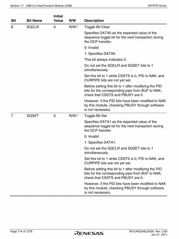
Section 17 USB 2.0 Host/Function Module (USB)
Page 714 of 1278 R01UH0234EJ0300 Rev. 3.00 Jun 21, 2011
SH7670 Group
Bit Bit Name Initial Value R/W Description
8 SQCLR 0 R/W*1 Toggle Bit Clear
Specifies DATA0 as the expected value of the sequence toggle bit for the next transaction during the DCP transfer.
0: Invalid
1: Specifies DATA0.
This bit always indicates 0.
Do not set the SQCLR and SQSET bits to 1 simultaneously.
Set this bit to 1 while CSSTS is 0, PID is NAK, and CURPIPE bits are not yet set.
Before setting this bit to 1 after modifying the PID bits for the corresponding pipe from BUF to NAK, check that CSSTS and PBUSY are 0.
However, if the PID bits have been modified to NAK by this module, checking PBUSY through software is not necessary.
7 SQSET 0 R/W*1 Toggle Bit Set
Specifies DATA1 as the expected value of the sequence toggle bit for the next transaction during the DCP transfer.
0: Invalid
1: Specifies DATA1.
Do not set the SQCLR and SQSET bits to 1 simultaneously.
Set this bit to 1 while CSSTS is 0, PID is NAK, and CURPIPE bits are not yet set.
Before setting this bit to 1 after modifying the PID bits for the corresponding pipe from BUF to NAK, check that CSSTS and PBUSY are 0.
However, if the PID bits have been modified to NAK by this module, checking PBUSY through software is not necessary.

Section 17 USB 2.0 Host/Function Module (USB)
R01UH0234EJ0300 Rev. 3.00 Page 715 of 1278 Jun 21, 2011
SH7670 Group
Bit Bit Name Initial Value R/W Description
6 SQMON 1 R Sequence Toggle Bit Monitor
Indicates the expected value of the sequence toggle bit for the next transaction during the DCP transfer.
0: DATA0
1: DATA1
This module allows this bit to toggle upon normal completion of the transaction. However, this bit is not allowed to toggle when a DATA-PID disagreement occurs during the transfer in the receiving direction.
When the function controller function is selected, this module sets this bit to 1 (specifies DATA1 as the expected value) upon normal reception of the setup packet.
When the function controller function is selected, this module does not reference to this bit during the IN/OUT transaction of the status stage, and does not allow this bit to toggle upon normal completion.
5 PBUSY 0 R Pipe Busy
This bit indicates whether DCP is used or not for the transaction when USB changes the PID bits from BUF to NAK.
0: DCP is not used for the transaction.
1: DCP is used for the transaction.
This module modifies this bit from 0 to 1 upon start of the USB transaction for the pertinent pipe, and modifies the bit from 1 to 0 upon completion of one transaction.
Reading this bit after software has set PID to NAK allows checking that modification of the pipe settings is possible.
For details, refer to (1) Pipe Control Register Switching Procedures under section 17.4.3, Pipe Control.

Section 17 USB 2.0 Host/Function Module (USB)
Page 716 of 1278 R01UH0234EJ0300 Rev. 3.00 Jun 21, 2011
SH7670 Group
Bit Bit Name Initial Value R/W Description
4 PINGE 0 R/W PING Token Issue Enable
When the host controller function is selected, setting this bit to 1 allows this module to issue the PING token during transfers in the transmitting direction and start a transfer in the transmitting direction with the PING transaction.
0: Disables issuing PING token.
1: Enables normal PING operation.
When having detected the ACK handshake during PING transactions, this module performs the OUT transaction as the next transaction.
When having detected the NAK handshake during OUT transactions, this module performs the PING transaction as the next transaction.
When the host controller function is selected, setting this bit to 0 through software prevents this module from issuing the PING token during transfers in the transmitting direction and only allows this module to perform OUT transactions for the transfers in the transmitting direction.
These bits should be modified while CSSTS is 0 and PID is NAK.
Before setting this bit to 1 after modifying the PID bits for the corresponding pipe from BUF to NAK, check that CSSTS and PBUSY are 0. However, if the PID bits have been modified to NAK by this module, checking PBUSY through software is not necessary.
When the function controller function is selected, be sure to write 0 to this bit.
3 ⎯ 0 R Reserved
This bit is always read as 0. The write value should always be 0.
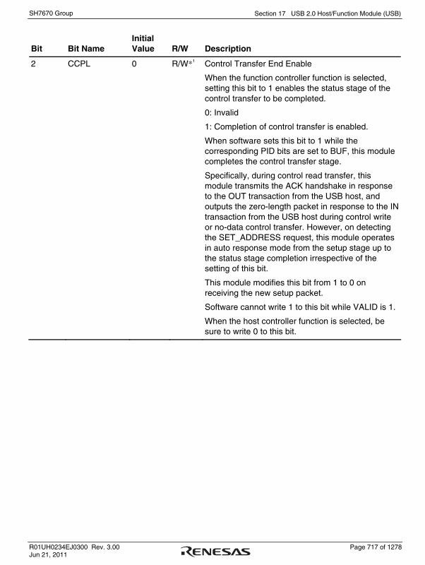
Section 17 USB 2.0 Host/Function Module (USB)
R01UH0234EJ0300 Rev. 3.00 Page 717 of 1278 Jun 21, 2011
SH7670 Group
Bit Bit Name Initial Value R/W Description
2 CCPL 0 R/W*1 Control Transfer End Enable
When the function controller function is selected, setting this bit to 1 enables the status stage of the control transfer to be completed.
0: Invalid
1: Completion of control transfer is enabled.
When software sets this bit to 1 while the corresponding PID bits are set to BUF, this module completes the control transfer stage.
Specifically, during control read transfer, this module transmits the ACK handshake in response to the OUT transaction from the USB host, and outputs the zero-length packet in response to the IN transaction from the USB host during control write or no-data control transfer. However, on detecting the SET_ADDRESS request, this module operates in auto response mode from the setup stage up to the status stage completion irrespective of the setting of this bit.
This module modifies this bit from 1 to 0 on receiving the new setup packet.
Software cannot write 1 to this bit while VALID is 1.
When the host controller function is selected, be sure to write 0 to this bit.

Section 17 USB 2.0 Host/Function Module (USB)
Page 718 of 1278 R01UH0234EJ0300 Rev. 3.00 Jun 21, 2011
SH7670 Group
Bit Bit Name Initial Value R/W Description
1, 0 PID[1:0] 00 R/W Response PID
Controls the response type of this module during control transfer.
00: NAK response
01: BUF response (depending on the buffer state)
10: STALL response
11: STALL response
(1) When the host controller function is selected
Modify the setting of these bits from NAK to BUF using the following procedure.
• When the transmitting direction is set
Write all the transmit data to the FIFO buffer while UACT is 1 and PID is NAK, and then set PID to BUF. After PID has been set to BUF, this module executes the OUT transaction (or PING transaction).
• When the receiving direction is set
Check that the FIFO buffer is empty (or empty the buffer) while UACT is 1 and PID is NAK, and then set PID to BUF. After PID has been set to BUF, this module executes the IN transaction.
This module modifies the setting of these bits as follows.
• This module sets PID to STALL (11) on receiving the data of the size exceeding the
maximum packet size when software has set
PID to BUF.
• This module sets PID to NAK on detecting a receive error such as a CRC error three
consecutive times.
• This module also sets PID to STALL (11) on
receiving the STALL handshake.

Section 17 USB 2.0 Host/Function Module (USB)
R01UH0234EJ0300 Rev. 3.00 Page 719 of 1278 Jun 21, 2011
SH7670 Group
Bit Bit Name Initial Value R/W Description
1, 0 PID[1:0] 00 R/W Even if software modifies the PID bits to NAK after this module has issued S-SPLIT of the split transaction for the selected pipe (while CSSTS indicates 1), this module continues the transaction until C-SPLIT completes. On completion of C-SPLIT, this module sets PID to NAK.
(2) When the function controller function is selected
This module modifies the setting of these bits as follows.
• This module modifies PID to NAK on receiving the setup packet. Here, this module sets VALID
to 1. Software cannot modify the setting of PID
until software sets VALID to 0.
• This module sets PID to STALL (11) on receiving the data of the size exceeding the
maximum packet size when software has set
PID to BUF.
• This module sets PID to STALL (1x) on
detecting the control transfer sequence error.
• This module sets PID to NAK on detecting the
USB bus reset.
This module does not reference to the setting of the PID bits while the SET_ADDRESS request is processed (auto processing).
Notes: 1. This bit is always read as 0. Only 1 can be written to.
2. Only 1 can be written to.

Section 17 USB 2.0 Host/Function Module (USB)
Page 720 of 1278 R01UH0234EJ0300 Rev. 3.00 Jun 21, 2011
SH7670 Group
17.3.31 Pipe Window Select Register (PIPESEL)
PIPE1 to PIPE 9 should be set using PIPESEL, PIPECFG, PIPEBUF, PIPEMAXP, PIPEPERI, PIPEnCTR, PIPEnTRE, and PIPEnTRN. After selecting the pipe using PIPESEL, functions of the pipe should be set using PIPECFG, PIPEBUF, PIPEMAXP, and PIPEPERI. PIPEnCTR, PIPEnTRE, and PIPEnTRN can be set regardless of the pipe selection in PIPESEL.
For a power-on reset and a USB bus reset, the corresponding bits for not only the selected pipe but all of the pipes are initialized.
This register is initialized by a power-on reset.
15 14 13 12 11 10 9 8 7 6 5 4 3 2 1 0Bit:
Initial value:R/W:
0 0 0 0 0 0 0 0 0 0 0 0 0 0 0 0R R R R R R R R R R R R R/W R/W R/W R/W
— — — — — — — — — — — — PIPESEL[3:0]
Bit Bit Name Initial Value R/W Description
15 to 4 ⎯ All 0 R Reserved
These bits are always read as 0. The write value should always be 0.

Section 17 USB 2.0 Host/Function Module (USB)
R01UH0234EJ0300 Rev. 3.00 Page 721 of 1278 Jun 21, 2011
SH7670 Group
Bit Bit Name Initial Value R/W Description
3 to 0 PIPESEL[3:0] 0000 R/W Pipe Window Select
Selects the pipe number corresponding to the PIPECFG, PIPEBUF, PIPEMAXP, and PIPEPERI registers which data is written to or read from.
0000: No pipe selected
0001: PIPE1
0010: PIPE2
0011: PIPE3
0100: PIPE4
0101: PIPE5
0110: PIPE6
0111: PIPE7
1000: PIPE8
1001: PIPE9
Other than above: Setting prohibited
Selecting a pipe number through these bits allows writing to and reading from the PIPECFG, PIPEBUF, PIPEMAXP, and PIPEPERI registers that correspond to the selected pipe number.
When PIPESEL = 0000, 0 is read from all of the bits in PIPECFG, PIPEBUF, PIPEMAXP, PIPEERI and PIPEnCTR. Writing to these bits is invalid.

Section 17 USB 2.0 Host/Function Module (USB)
Page 722 of 1278 R01UH0234EJ0300 Rev. 3.00 Jun 21, 2011
SH7670 Group
17.3.32 Pipe Configuration Register (PIPECFG)
PIPECFG is a register that specifies the transfer type, buffer memory access direction, and endpoint numbers for PIPE1 to PIPE9. It also selects continuous or non-continuous transfer mode, single or double buffer mode, and whether to continue or disable pipe operation at the end of transfer.
This register is initialized by a power-on reset. Only the TYPE[1:0] bits are initialized by a USB bus reset.
15 14 13 12 11 10 9 8 7 6 5 4 3 2 1 0Bit:
Initial value:R/W:
0 0 0 0 0 0 0 0 0 0 0 0 0 0 0 0R/W R/W R R R R/W R/W R/W R/W R R R/W R/W R/W R/W R/W
TYPE[1:0] — — — BFRE DBLB CNTMD SHTNAK — — DIR EPNUM[3:0]

Section 17 USB 2.0 Host/Function Module (USB)
R01UH0234EJ0300 Rev. 3.00 Page 723 of 1278 Jun 21, 2011
SH7670 Group
Bit Bit Name Initial Value R/W Description
15, 14 TYPE[1:0] 00 R/W Transfer Type
Selects the transfer type for the pipe selected by the PIPESEL bits (selected pipe)
• PIPE1 and PIPE2
00: Pipe not used
01: Bulk transfer
10: Setting prohibited
11: Isochronous transfer
• PIPE3 to PIPE5
00: Pipe not used
01: Bulk transfer
10: Setting prohibited
11: Setting prohibited
• PIPE6 and PIPE7
00: Pipe not used
01: Setting prohibited
10: Interrupt transfer
11: Setting prohibited
Before setting PID to BUF for the selected pipe (before starting USB communication using the selected pipe), be sure to set these bits to the value other than 00.
Modify these bits while the PID bits for the selected pipe are set to NAK. Before modifying these bits after modifying the PID bits for the selected pipe from BUF to NAK, check that CSSTS and PBUSY are 0. However, if the PID bits have been modified to NAK by this module, checking PBUSY through software is not necessary.
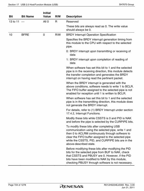
Section 17 USB 2.0 Host/Function Module (USB)
Page 724 of 1278 R01UH0234EJ0300 Rev. 3.00 Jun 21, 2011
SH7670 Group
Bit Bit Name Initial Value R/W Description
13 to 11 ⎯ All 0 R Reserved
These bits are always read as 0. The write value should always be 0.
10 BFRE 0 R/W BRDY Interrupt Operation Specification
Specifies the BRDY interrupt generation timing from this module to the CPU with respect to the selected pipe.
0: BRDY interrupt upon transmitting or receiving of data
1: BRDY interrupt upon completion of reading of data
When software has set this bit to 1 and the selected pipe is in the receiving direction, this module detects the transfer completion and generates the BRDY interrupt on having read the pertinent packet.
When the BRDY interrupt is generated with the above conditions, software needs to write 1 to BCLR. The FIFO buffer assigned to the selected pipe is not enabled for reception until 1 is written to BCLR.
When software has set this bit to 1 and the selected pipe is in the transmitting direction, this module does not generate the BRDY interrupt.
For details, refer to (1) BRDY Interrupt under section 17.4.2, Interrupt Functions.
Modify these bits while CSSTS is 0 and PID is NAK and before the pipe is selected by the CURPIPE bits.
To modify these bits after completing USB communication using the selected pipe, write 1 and then 0 to ACLRM continuously through software to clear the FIFO buffer assigned to the selected pipe while the CSSTS, PID, and CURPIPE bits are in the above-described state.
Before modifying these bits after modifying the PID bits for the selected pipe from BUF to NAK, check that CSSTS and PBUSY are 0. However, if the PID bits have been modified to NAK by this module, checking PBUSY through software is not necessary.

Section 17 USB 2.0 Host/Function Module (USB)
R01UH0234EJ0300 Rev. 3.00 Page 725 of 1278 Jun 21, 2011
SH7670 Group
Bit Bit Name Initial Value R/W Description
9 DBLB 0 R/W Double Buffer Mode
Selects either single or double buffer mode for the FIFO buffer used by the selected pipe.
0: Single buffer
1: Double buffer
This bit is valid when PIPE1 to PIPE5 are selected.
When software has set this bit to 1, this module assigns two planes of the FIFO buffer size specified by the BUFSIZE bits in PIPEBUF to the selected pipe.
Specifically, the following expression determines the FIFO buffer size assigned to the selected pipe by this module.
(BUFSIZE + 1) * 64 * (DBLB + 1) [bytes]
When software has set this bit to 1 and the selected pipe is in the transmitting direction, this module does not generate the BRDY interrupt.
For details, refer to (1) BRDY Interrupt under section 17.4.2, Interrupt Functions.
Modify these bits while CSSTS is 0 and PID is NAK and before the pipe is selected by the CURPIPE bits.
To modify these bits after completing USB communication using the selected pipe, write 1 and then 0 to ACLRM continuously through software to clear the FIFO buffer assigned to the selected pipe while the CSSTS, PID, and CURPIPE bits are in the above-described state.
Before modifying these bits after modifying the PID bits for the selected pipe from BUF to NAK, check that CSSTS and PBUSY are 0. However, if the PID bits have been modified to NAK by this module, checking PBUSY through software is not necessary.
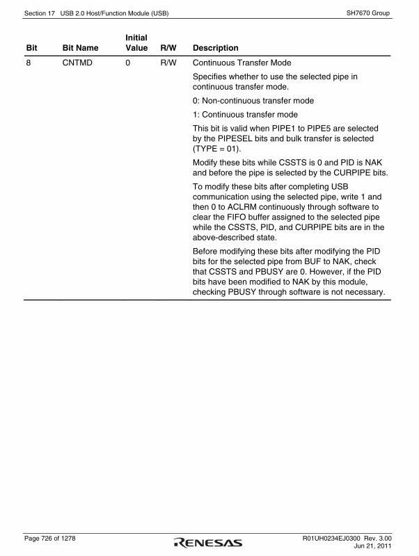
Section 17 USB 2.0 Host/Function Module (USB)
Page 726 of 1278 R01UH0234EJ0300 Rev. 3.00 Jun 21, 2011
SH7670 Group
Bit Bit Name Initial Value R/W Description
8 CNTMD 0 R/W Continuous Transfer Mode
Specifies whether to use the selected pipe in continuous transfer mode.
0: Non-continuous transfer mode
1: Continuous transfer mode
This bit is valid when PIPE1 to PIPE5 are selected by the PIPESEL bits and bulk transfer is selected (TYPE = 01).
Modify these bits while CSSTS is 0 and PID is NAK and before the pipe is selected by the CURPIPE bits.
To modify these bits after completing USB communication using the selected pipe, write 1 and then 0 to ACLRM continuously through software to clear the FIFO buffer assigned to the selected pipe while the CSSTS, PID, and CURPIPE bits are in the above-described state.
Before modifying these bits after modifying the PID bits for the selected pipe from BUF to NAK, check that CSSTS and PBUSY are 0. However, if the PID bits have been modified to NAK by this module, checking PBUSY through software is not necessary.

Section 17 USB 2.0 Host/Function Module (USB)
R01UH0234EJ0300 Rev. 3.00 Page 727 of 1278 Jun 21, 2011
SH7670 Group
Bit Bit Name Initial Value R/W Description
7 SHTNAK 0 R/W Pipe Disabled at End of Transfer
Specifies whether to modify PID to NAK upon the end of transfer when the selected pipe is in the receiving direction.
0: Pipe continued at the end of transfer
1: Pipe disabled at the end of transfer
This bit is valid when the selected pipe is PIPE1 to PIPE5 in the receiving direction.
When software has set this bit to 1 for the selected pipe in the receiving direction, this module modifies the PID bits corresponding to the selected pipe to NAK on determining the end of the transfer. This module determines that the transfer has ended on any of the following conditions.
• A short packet (including a zero-length packet) is
successfully received.
• The transaction counter is used and the number of packets specified by the counter are
successfully received.
Modify these bits while CSSTS is 0 and PID is NAK.
Before modifying these bits after modifying the PID bits for the selected pipe from BUF to NAK, check that CSSTS and PBUSY are 0. However, if the PID bits have been modified to NAK by this module, checking PBUSY through software is not necessary.
This bit should be cleared to 0 for the pipe in the transmitting direction.
6, 5 ⎯ All 0 R Reserved
These bits are always read as 0. The write value should always be 0.

Section 17 USB 2.0 Host/Function Module (USB)
Page 728 of 1278 R01UH0234EJ0300 Rev. 3.00 Jun 21, 2011
SH7670 Group
Bit Bit Name Initial Value R/W Description
4 DIR 0 R/W Transfer Direction
Specifies the transfer direction for the selected pipe.
0: Receiving direction
1: Sending direction
When software has set this bit to 0, this module uses the selected pipe in the receiving direction, and when software has set this bit to 1, this module uses the selected pipe in the transmitting direction.
Modify these bits while CSSTS is 0 and PID is NAK and before the pipe is selected by the CURPIPE bits.
To modify these bits after completing USB communication using the selected pipe, write 1 and then 0 to ACLRM continuously through software to clear the FIFO buffer assigned to the selected pipe while the CSSTS, PID, and CURPIPE bits are in the above-described state.
Before modifying these bits after modifying the PID bits for the selected pipe from BUF to NAK, check that CSSTS and PBUSY are 0. However, if the PID bits have been modified to NAK by this module, checking PBUSY through software is not necessary.
3 to 0 EPNUM[3:0] 0000 R/W Endpoint Number
These bits specify the endpoint number for the selected pipe.
Setting 0000 means unused pipe.
Modify these bits while CSSTS is 0 and PID is NAK.
Before modifying these bits after modifying the PID bits for the selected pipe from BUF to NAK, check that CSSTS and PBUSY are 0. However, if the PID bits have been modified to NAK by this module, checking PBUSY through software is not necessary.
Do not make the settings such that the combination of the set values in the DIR and EPNUM bits should be the same for two or more pipes (EPNUM = 0000 can be set for all the pipes).

Section 17 USB 2.0 Host/Function Module (USB)
R01UH0234EJ0300 Rev. 3.00 Page 729 of 1278 Jun 21, 2011
SH7670 Group
17.3.33 Pipe Buffer Setting Register (PIPEBUF)
PIPEBUF is a register that specifies the buffer size and buffer number for PIPE1 to PIPE9.
This register is initialized by a power-on reset.
15 14 13 12 11 10 9 8 7 6 5 4 3 2 1 0Bit:
Initial value:R/W:
0 0 0 0 0 0 0 0 0 0 0 0 0 0 0 0R R/W R/W R/W R/W R/W R R R/W R/W R/W R/W R/W R/W R/W R/W
— BUFSIZE[4:0] — — BUFNMB[7:0]
Bit Bit Name Initial Value R/W Description
15 ⎯ 0 R Reserved
This bit is always read as 0. The write value should always be 0.

Section 17 USB 2.0 Host/Function Module (USB)
Page 730 of 1278 R01UH0234EJ0300 Rev. 3.00 Jun 21, 2011
SH7670 Group
Bit Bit Name Initial Value R/W Description
14 to 10 BUFSIZE[4:0] H'00 R/W Buffer Size
Specifies the size of the buffer for the pipe selected by the PIPESEL bits (selected pipe) in terms of blocks, where one block comprises 64 bytes.
00000 (H'00): 64 bytes
00001 (H'01): 128 bytes
: :
11111 (H'1F): 2 Kbytes
When software has set the DBLB bit to 1, this module assigns two planes of the FIFO buffer size specified by the BUFSIZE bits to the selected pipe.
Specifically, the following expression determines the FIFO buffer size assigned to the selected pipe by this module.
(BUFSIZE + 1) * 64 * (DBLB + 1) [bytes]
The valid value for these bits depends on the selected pipe.
• PIPE1 to PIPE5: Any value from H'00 to H'1F is
valid.
• PIPE6 to PIPE9: H'00 should be set.
When used with CNTMD = 1, set an integer multiple of the maximum packet size to the BUFSIZE bits.
Modify these bits while CSSTS is 0 and PID is NAK and before the pipe is selected by the CURPIPE bits.
Before modifying these bits after modifying the PID bits for the selected pipe from BUF to NAK, check that CSSTS and PBUSY are 0. However, if the PID bits have been modified to NAK by this module, checking PBUSY through software is not necessary.
9, 8 ⎯ All 0 R Reserved
These bits are always read as 0. The write value should always be 0.
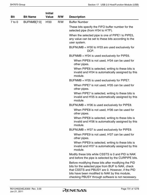
Section 17 USB 2.0 Host/Function Module (USB)
R01UH0234EJ0300 Rev. 3.00 Page 731 of 1278 Jun 21, 2011
SH7670 Group
Bit Bit Name Initial Value R/W Description
7 to 0 BUFNMB[7:0] H'00 R/W Buffer Number
These bits specify the FIFO buffer number for the selected pipe (from H'04 to H'7F).
When the selected pipe is one of PIPE1 to PIPE5, any value can be set to these bits according to the user system.
BUFNUMB = H'00 to H'03 are used exclusively for DCP.
BUFNMB = H'04 is used exclusively for PIPE6.
When PIPE6 is not used, H'04 can be used for other pipes.
When PIPE6 is selected, writing to these bits is invalid and H'04 is automatically assigned by this module.
BUFNMB = H'05 is used exclusively for PIPE7.
When PIPE7 is not used, H'05 can be used for other pipes.
When PIPE7 is selected, writing to these bits is invalid and H'05 is automatically assigned by this module.
BUFNUMB = H'06 is used exclusively for PIPE8.
When PIPE8 is not used, H'06 can be used for other pipes.
When PIPE8 is selected, writing to these bits is invalid and H'06 is automatically assigned by this module.
BUFNUMB = H'07 is used exclusively for PIPE9.
When PIPE9 is not used, H'07 can be used for other pipes.
When PIPE9 is selected, writing to these bits is invalid and H'07 is automatically assigned by this module.
Modify these bits while CSSTS is 0 and PID is NAK and before the pipe is selected by the CURPIPE bits.
Before modifying these bits after modifying the PID bits for the selected pipe from BUF to NAK, check that CSSTS and PBUSY are 0. However, if the PID bits have been modified to NAK by this module, checking PBUSY through software is not necessary.

Section 17 USB 2.0 Host/Function Module (USB)
Page 732 of 1278 R01UH0234EJ0300 Rev. 3.00 Jun 21, 2011
SH7670 Group
17.3.34 Pipe Maximum Packet Size Register (PIPEMAXP)
PIPEMAXP is a register that specifies the maximum packet size for PIPE1 to PIPE9.
This register is initialized by a power-on reset.
15 14 13 12 11 10 9 8 7 6 5 4 3 2 1 0Bit:
Initial value:R/W:
0 0 0 0 0 0 0 0 0 0 0 0 0 0 0 0R/W R/W R/W R/W R R/W R/W R/W R/W R/W R/W R/W R/W R/W R/W R/W
— MXPS[10:0]DEVSEL[3:0]
Bit Bit Name Initial Value R/W Description
15 to 12 DEVSEL[3:0] 00 R/W Device Select
When the host controller function is selected, these bits specify the USB address of the communication target peripheral device.
0000: Address 0000
0001: Address 0001
0010: Address 0010
: :
1010: Address 1010
Other than above: Setting prohibited
These bits should be set after setting the address to the DEVADDn register corresponding to the value to be set in these bits.
For example, before setting DEVSEL to 0010, the address should be set to the DEVADD2 register.
Before modifying these bits after modifying the PID bits for the selected pipe from BUF to NAK, check that CSSTS and PBUSY are 0. However, if the PID bits have been modified to NAK by this module, checking PBUSY through software is not necessary.
When the function controller function is selected, these bits should be set to B'0000.
11 ⎯ 0 R Reserved
This bit is always read as 0. The write value should always be 0.

Section 17 USB 2.0 Host/Function Module (USB)
R01UH0234EJ0300 Rev. 3.00 Page 733 of 1278 Jun 21, 2011
SH7670 Group
Bit Bit Name Initial Value R/W Description
10 to 0 MXPS[10:0] * R/W Maximum Packet Size
Specifies the maximum data payload (maximum packet size) for the selected pipe. The valid value for these bits depends on the pipe as follows.
PIPE1, PIPE2: 1 byte (H'001) to 1,024 bytes (H'400)
PIPE3 to PIPE5: 8 bytes (H'008), 16 bytes (H'010), 32 bytes (H'020), 64 bytes (H'040), and 512 bytes (H'200) (Bits 2 to 0 are not provided.)
PIPE6 to PIPE9: 1 byte (H'001) to 64 bytes (H'040)
These bits should be set to the appropriate value for each transfer type based on the USB Specification.
For split transactions using the isochronous pipe, these bits should be set to 188 bytes or less.
Before modifying these bits after modifying the PID bits for the selected pipe from BUF to NAK, check that CSSTS and PBUSY are 0. However, if the PID bits have been modified to NAK by this module, checking PBUSY through software is not necessary.
While MXPS is 0, do not write to the FIFO buffer or set PID to BUF.
Note: * The initial value of MXPS is H'000 when no pipe is selected with the PIPESEL bits in PIPESEL and H'040 when a pipe is selected with the PIPESEL bit in PIPESEL.

Section 17 USB 2.0 Host/Function Module (USB)
Page 734 of 1278 R01UH0234EJ0300 Rev. 3.00 Jun 21, 2011
SH7670 Group
17.3.35 Pipe Timing Control Register (PIPEPERI)
PIPEPERI is a register that selects whether the buffer is flushed or not when an interval error occurred during isochronous IN transfer, and sets the interval error detection interval for PIPE1 to PIPE9.
This register is initialized by a power-on reset.
15 14 13 12 11 10 9 8 7 6 5 4 3 2 1 0Bit:
Initial value:R/W:
0 0 0 0 0 0 0 0 0 0 0 0 0 0 0 0R R R R/W R R R R R R R R R R/W R/W R/W
— — — IFIS — — — — — — — — — IITV[2:0]
Bit Bit Name Initial Value R/W Description
15 to 13 ⎯ All 0 R Reserved
These bits are always read as 0. The write value should always be 0.
12 IFIS 0 R/W Isochronous IN Buffer Flush
Specifies whether to flush the buffer when the pipe selected by the PIPESEL bits (selected pipe) is used for isochronous IN transfers.
0: The buffer is not flushed.
1: The buffer is flushed.
When the function controller function is selected and the selected pipe is for isochronous IN transfers, this module automatically clears the FIFO buffer when this module fails to receive the IN token from the USB host within the interval set by the IITV bits in terms of (μ) frames.
In double buffer mode (DBLB = 1), this module only clears the data in the plane used earlier.
This module clears the FIFO buffer on receiving the SOF packet immediately after the (μ) frame in which this module has expected to receive the IN token. Even if the SOF packet is corrupted, this module also clears the FIFO buffer at the right timing to receive the SOF packet by using the internal interpolation.
When the host controller function is selected, set this bit to 0.
When the selected pipe is not for the isochronous transfer, set this bit to 0.

Section 17 USB 2.0 Host/Function Module (USB)
R01UH0234EJ0300 Rev. 3.00 Page 735 of 1278 Jun 21, 2011
SH7670 Group
Bit Bit Name Initial Value R/W Description
11 to 3 ⎯ All 0 R Reserved
These bits are always read as 0. The write value should always be 0.
2 to 0 IITV[2:0] 000 R/W Interval Error Detection Interval
Specifies the interval error detection timing for the selected pipe in terms of frames, which is expressed as n-th power of 2 (n is the value to be set).
As described later, the detailed functions are different in host controller mode and in function controller mode.
Modify these bits while CSSTS is 0 and PID is NAK and before the pipe is selected by the CURPIPE bits.
Before modifying these bits after modifying the PID bits for the selected pipe from BUF to NAK, check that CSSTS and PBUSY are 0. However, if the PID bits have been modified to NAK by this module, checking PBUSY through software is not necessary.
Before modifying these bits after USB communication has been completed with these bits set to a certain value, set PID to NAK and then set ACLRM to 1 to initialize the interval timer.
The IITV bits are invalid for PIPE3 to PIPE5; set these bits to 000 for these pipes.
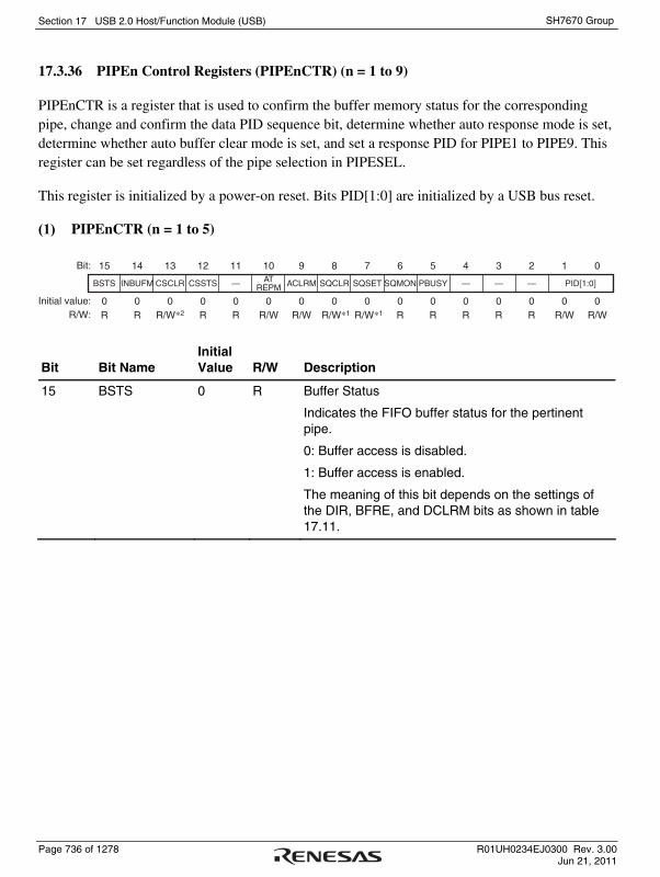
Section 17 USB 2.0 Host/Function Module (USB)
Page 736 of 1278 R01UH0234EJ0300 Rev. 3.00 Jun 21, 2011
SH7670 Group
17.3.36 PIPEn Control Registers (PIPEnCTR) (n = 1 to 9)
PIPEnCTR is a register that is used to confirm the buffer memory status for the corresponding pipe, change and confirm the data PID sequence bit, determine whether auto response mode is set, determine whether auto buffer clear mode is set, and set a response PID for PIPE1 to PIPE9. This register can be set regardless of the pipe selection in PIPESEL.
This register is initialized by a power-on reset. Bits PID[1:0] are initialized by a USB bus reset.
(1) PIPEnCTR (n = 1 to 5)
15 14 13 12 11 10 9 8 7 6 5 4 3 2 1 0Bit:
Initial value:R/W:
0 0 0 0 0 0 0 0 0 0 0 0 0 0 0 0R R R/W*2 R R R/W R/W R/W*1 R/W*1 R R R R R R/W R/W
BSTS INBUFM CSCLR CSSTS — ATREPM ACLRM SQCLR SQSET SQMON PBUSY — — — PID[1:0]
Bit Bit Name Initial Value R/W Description
15 BSTS 0 R Buffer Status
Indicates the FIFO buffer status for the pertinent pipe.
0: Buffer access is disabled.
1: Buffer access is enabled.
The meaning of this bit depends on the settings of the DIR, BFRE, and DCLRM bits as shown in table 17.11.
Section 17 USB 2.0 Host/Function Module (USB)
R01UH0234EJ0300 Rev. 3.00 Page 737 of 1278 Jun 21, 2011
SH7670 Group
Bit Bit Name Initial Value R/W Description
14 INBUFM 0 R IN Buffer Monitor
Indicates the pertinent FIFO buffer status when the pertinent pipe is in the transmitting direction.
0: There is no data to be transmitted in the buffer memory.
1: There is data to be transmitted in the buffer memory.
When the pertinent pipe is in the transmitting direction (DIR = 1), this module sets this bit to 1 when software (or DMAC) completes writing data to at least one FIFO buffer plane.
This module sets this bit to 0 when this module completes transmitting the data from the FIFO buffer plane to which all the data has been written. In double buffer mode (DBLB = 1), this module sets this bit to 0 when this module completes transmitting the data from the two FIFO buffer planes before software (or DMAC) completes writing data to one FIFO buffer plane.
This bit indicates the same value as the BSTS bit when the pertinent pipe is in the receiving direction (DIR = 0).
Section 17 USB 2.0 Host/Function Module (USB)
Page 738 of 1278 R01UH0234EJ0300 Rev. 3.00 Jun 21, 2011
SH7670 Group
Bit Bit Name Initial Value R/W Description
13 CSCLR 0 R/W*2 C-SPLIT Status Clear Bit
When the host controller function is selected, setting this bit to 1 through software allows this module to clear the CSSTS bit to 0.
0: Writing invalid
1: Clears the CSSTS bit to 0.
For the transfer using the split transaction, to restart the next transfer with the S-SPLIT forcibly, set this bit to 1 through software. However, for the normal split transaction, this module automatically clears the CSSTS bit to 0 upon completion of the C-SPLIT; therefore, clearing the CSSTS bit through software is not necessary.
Controlling the CSSTS bit through this bit must be done while UACT is 0 and thus communication is halted or while no transfer is being performed with bus disconnection detected.
Setting this bit to 1 while CSSTS is 0 has no effect.
When the function controller function is selected, be sure to write 0 to this bit.
12 CSSTS 0 R CSSTS Status Bit
Indicates the C-SPLIT status of the split transaction when the host controller function is selected.
0: START-SPLIT (S-SPLIT) transaction being processed or the transfer not using the split transaction in progress
1: C-SPLIT transaction being processed
This module sets this bit to 1 upon start of the C-SPLIT and clears this bit to 0 upon detection of C-SPLIT completion.
Indicates the valid value only when the host controller function is selected.
11 ⎯ 0 R Reserved
This bit is always read as 0. The write value should always be 0.
Section 17 USB 2.0 Host/Function Module (USB)
R01UH0234EJ0300 Rev. 3.00 Page 739 of 1278 Jun 21, 2011
SH7670 Group
Bit Bit Name Initial Value R/W Description
10 ATREPM 0 R/W Auto Response Mode
Enables or disables auto response mode for the pertinent pipe.
0: Auto response disabled
1: Auto response enabled
When the function controller function is selected and the pertinent pipe is for bulk transfer, this bit can be set to 1.
When this bit is set to 1, this module responds to the token from the USB host as described below.
(1) When the pertinent pipe is for bulk IN transfer (TYPE = 01 and DIR = 1)
When ATREPM = 1 and PID = BUF, this module transmits a zero-length packet in response to the IN token.
This module updates (allows toggling of) the sequence toggle bit (DATA-PID) each time this module receives the ACK from the USB host (in a single transaction, IN token is received, zero-length packet is transmitted, and then ACK is received.).
In this case, this module does not generate the BRDY or BEMP interrupt.
(2) When the pertinent pipe is for bulk OUT transfer (TYPE = 01 and DIR = 0)
When ATREPM = 1 and PID = BUF, this module returns NAK in response to the OUT (or PING) token and generates the NRDY interrupt.
Modify this bit while CSSTS is 0 and PID is NAK. Before modifying this bit after modifying the PID bits for the corresponding pipe from BUF to NAK, check that CSSTS and PBUSY are 0. However, if the PID bits have been modified to NAK by this module, checking PBUSY through software is not necessary.

Section 17 USB 2.0 Host/Function Module (USB)
Page 740 of 1278 R01UH0234EJ0300 Rev. 3.00 Jun 21, 2011
SH7670 Group
Bit Bit Name Initial Value R/W Description
10 ATREPM 0 R/W For USB communication in auto response mode, set this bit to 1 while the FIFO buffer is empty. Do not write to the FIFO buffer during USB communication in auto response mode.
When the pertinent pipe is for isochronous transfer, be sure to set this bit to 0.
When the host controller function is selected, set this bit to 0.
9 ACLRM 0 R/W Auto Buffer Clear Mode
Enables or disables automatic buffer clear mode for the pertinent pipe.
0: Disabled
1: Enabled (all buffers are initialized)
To delete the information in the FIFO buffer assigned to the pertinent pipe completely, write 1 and then 0 to this bit continuously.
Table 17.12 shows the information cleared by writing 1 and 0 to this bit continuously and the cases in which clearing the information is necessary.
Modify this bit while CSSTS is 0 and PID is NAK.
Before modifying this bit after modifying the PID bits for the corresponding pipe from BUF to NAK, check that CSSTS and PBUSY are 0. However, if the PID bits have been modified to NAK by this module, checking PBUSY through software is not necessary.
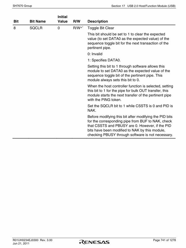
Section 17 USB 2.0 Host/Function Module (USB)
R01UH0234EJ0300 Rev. 3.00 Page 741 of 1278 Jun 21, 2011
SH7670 Group
Bit Bit Name Initial Value R/W Description
8 SQCLR 0 R/W*1 Toggle Bit Clear
This bit should be set to 1 to clear the expected value (to set DATA0 as the expected value) of the sequence toggle bit for the next transaction of the pertinent pipe.
0: Invalid
1: Specifies DATA0.
Setting this bit to 1 through software allows this module to set DATA0 as the expected value of the sequence toggle bit of the pertinent pipe. This module always sets this bit to 0.
When the host controller function is selected, setting this bit to 1 for the pipe for bulk OUT transfer, this module starts the next transfer of the pertinent pipe with the PING token.
Set the SQCLR bit to 1 while CSSTS is 0 and PID is NAK.
Before modifying this bit after modifying the PID bits for the corresponding pipe from BUF to NAK, check that CSSTS and PBUSY are 0. However, if the PID bits have been modified to NAK by this module, checking PBUSY through software is not necessary.

Section 17 USB 2.0 Host/Function Module (USB)
Page 742 of 1278 R01UH0234EJ0300 Rev. 3.00 Jun 21, 2011
SH7670 Group
Bit Bit Name Initial Value R/W Description
7 SQSET 0 R/W*1 Toggle Bit Set
This bit should be set to 1 to setDATA1 as the expected value of the sequence toggle bit for the next transaction of the pertinent pipe.
0: Invalid
1: Specifies DATA1.
Setting this bit to 1 through software allows this module to set DATA1 as the expected value of the sequence toggle bit of the pertinent pipe. This module always sets this bit to 0.
Set the SQSET bit to 1 while CSSTS is 0 and PID is NAK.
Before modifying this bit after modifying the PID bits for the corresponding pipe from BUF to NAK, check that CSSTS and PBUSY are 0. However, if the PID bits have been modified to NAK by this module, checking PBUSY through software is not necessary.
6 SQMON 0 R Toggle Bit Confirmation
Indicates the expected value of the sequence toggle bit for the next transaction of the pertinent pipe.
0: DATA0
1: DATA1
When the pertinent pipe is not for the isochronous transfer, this module allows this bit to toggle upon normal completion of the transaction. However, this bit is not allowed to toggle when a DATA-PID disagreement occurs during the receiving transfer.

Section 17 USB 2.0 Host/Function Module (USB)
R01UH0234EJ0300 Rev. 3.00 Page 743 of 1278 Jun 21, 2011
SH7670 Group
Bit Bit Name Initial Value R/W Description
5 PBUSY 0 R Pipe Busy
This bit indicates whether the relevant pipe is used or not for the transaction.
0: The relevant pipe is not used for the transaction.
1: The relevant pipe is used for the transaction.
This module modifies this bit from 0 to 1 upon start of the USB transaction for the pertinent pipe, and modifies the bit from 1 to 0 upon completion of one transaction.
Reading this bit after software has set PID to NAK allows checking that modification of the pipe settings is possible.
For details, refer to (1) Pipe Control Register Switching Procedures under section 17.4.3, Pipe Control.
4 to 2 ⎯ All 0 R Reserved
These bits are always read as 0. The write value should always be 0.

Section 17 USB 2.0 Host/Function Module (USB)
Page 744 of 1278 R01UH0234EJ0300 Rev. 3.00 Jun 21, 2011
SH7670 Group
Bit Bit Name Initial Value R/W Description
1, 0 PID[1:0] 00 R/W Response PID
Specifies the response type for the next transaction of the pertinent pipe.
00: NAK response
01: BUF response (depending on the buffer state)
10: STALL response
11: STALL response
The default setting of these bits is NAK. Modify the setting to BUF to use the pertinent pipe for USB transfer. Tables 17.13 and 17.14 show the basic operation (operation when there are no errors in the transmitted and received packets) of this module depending on the PID bit setting.
After modifying the setting of these bits through software from BUF to NAK during USB communication using the pertinent pipe, check that PBUSY is 1 to see if USB communication using the pertinent pipe has actually entered the NAK state. However, if the PID bits have been modified to NAK by this module, checking PBUSY through software is not necessary.
Notes: 1. Only 0 can be read and 1 can be written to.
2. Only 1 can be written to.

Section 17 USB 2.0 Host/Function Module (USB)
R01UH0234EJ0300 Rev. 3.00 Page 745 of 1278 Jun 21, 2011
SH7670 Group
Table 17.11 Meaning of BSTS Bit
DIR Bit BFRE Bit DCLRM Bit Meaning of BSTS Bit
0 0 0 1: The received data can be read from the FIFO buffer.
0: The received data has been completely read from the FIFO buffer.
1 Setting prohibited
1 0 1: The received data can be read from the FIFO buffer.
0: Software has set BCLR to 1 after the received data has been completely read from the FIFO buffer.
1 1: The received data can be read from the FIFO buffer.
0: The received data has been completely read from the FIFO buffer.
1 0 0 1: The transmit data can be written to the FIFO buffer.
0: The transmit data has been completely written to the FIFO buffer.
1 Setting prohibited
1 0 Setting prohibited
1 Setting prohibited
Table 17.12 Information Cleared by this Module by Setting ACLRM = 1
No. Information Cleared by ACLRM Bit Manipulation
Cases in which Clearing the Information is Necessary
1 All the information in the FIFO buffer assigned to the pertinent pipe (all the information in two FIFO buffer planes in double buffer mode)
2 The interval count value when the pertinent pipe is for isochronous transfer
When the interval count value is to be reset
3 Values of the internal flags related to the BFRE bit
When the BFRE setting is modified
4 FIFO buffer toggle control When the DBLB setting is modified
5 Values of the internal flags related to the transaction count
When the transaction count function is forcibly terminated

Section 17 USB 2.0 Host/Function Module (USB)
Page 746 of 1278 R01UH0234EJ0300 Rev. 3.00 Jun 21, 2011
SH7670 Group
Table 17.13 Operation of This Module depending on PID Setting (when Host Controller Function is Selected)
PID Transfer Type Transfer Direction(DIR Bit) Operation of This Module
00 (NAK) Operation does not depend on the setting.
Operation does not depend on the setting.
Does not issue tokens.
01 (BUF) Bulk or interrupt Operation does not depend on the setting.
Issues tokens while UACT is 1 and the FIFO buffer corresponding to the pertinent pipe is ready for transmission and reception.
Does not issue tokens while UACT is 0 or the FIFO buffer corresponding to the pertinent pipe is not ready for transmission or reception.
Isochronous Operation does not depend on the setting.
Issues tokens irrespective of the status of the FIFO buffer corresponding to the pertinent pipe.
10 (STALL) or 11 (STALL)
Operation does not depend on the setting.
Operation does not depend on the setting.
Does not issue tokens.
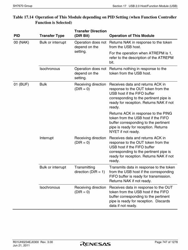
Section 17 USB 2.0 Host/Function Module (USB)
R01UH0234EJ0300 Rev. 3.00 Page 747 of 1278 Jun 21, 2011
SH7670 Group
Table 17.14 Operation of This Module depending on PID Setting (when Function Controller Function is Selected)
PID Transfer Type Transfer Direction(DIR Bit) Operation of This Module
00 (NAK) Bulk or interrupt Operation does not depend on the setting.
Returns NAK in response to the token from the USB host.
For the operation when ATREPM is 1, refer to the description of the ATREPM bit.
Isochronous Operation does not depend on the setting.
Returns nothing in response to the token from the USB host.
01 (BUF) Bulk Receiving direction (DIR = 0)
Receives data and returns ACK in response to the OUT token from the USB host if the FIFO buffer corresponding to the pertinent pipe is ready for reception. Returns NAK if not ready.
Returns ACK in response to the PING token from the USB host if the FIFO buffer corresponding to the pertinent pipe is ready for reception. Returns NYET if not ready.
Interrupt Receiving direction (DIR = 0)
Receives data and returns ACK in response to the OUT token from the USB host if the FIFO buffer corresponding to the pertinent pipe is ready for reception. Returns NAK if not ready.
Bulk or interrupt Transmitting direction (DIR = 1)
Transmits data in response to the token from the USB host if the corresponding FIFO buffer is ready for transmission. Returns NAK if not ready.
Isochronous Receiving direction (DIR = 0)
Receives data in response to the OUT token from the USB host if the FIFO buffer corresponding to the pertinent pipe is ready for reception. Discards data if not ready.

Section 17 USB 2.0 Host/Function Module (USB)
Page 748 of 1278 R01UH0234EJ0300 Rev. 3.00 Jun 21, 2011
SH7670 Group
PID Transfer Type Transfer Direction(DIR Bit) Operation of This Module
01 (BUF) Isochronous Transmitting direction (DIR = 1)
Transmits data in response to the token from the USB host if the corresponding FIFO buffer is ready for transmission. Transmits the zero-length packet if not ready.
10 (STALL) or 11 (STALL)
Bulk or interrupt Operation does not depend on the setting.
Returns STALL in response to the token from the USB host.
Isochronous Operation does not depend on the setting
Returns nothing in response to the token from the USB host.
(2) PIPEnCTR (n = 6 to 9)
15 14 13 12 11 10 9 8 7 6 5 4 3 2 1 0Bit:
Initial value:R/W:
0 0 0 0 0 0 0 0 0 0 0 0 0 0 0 0R R R/W*1 R/W R R R/W R/W*1 R/W*1 R R R R R R/W R/W
BSTS — CSCLR CSSTS — — ACLRM SQCLR SQSET SQMON PBUSY — — — PID[1:0]
Bit Bit Name Initial Value R/W Description
15 BSTS 0 R Buffer Status
Indicates the FIFO buffer status for the pertinent pipe.
0: Buffer access is disabled.
1: Buffer access is enabled.
The meaning of this bit depends on the settings of the DIR, BFRE, and DCLRM bits as shown in table 17.11.
14 ⎯ 0 R Reserved
This bit is always read as 0. The write value should always be 0.

Section 17 USB 2.0 Host/Function Module (USB)
R01UH0234EJ0300 Rev. 3.00 Page 749 of 1278 Jun 21, 2011
SH7670 Group
Bit Bit Name Initial Value R/W Description
13 CSCLR 0 R/W*1 C-SPLIT Status Clear Bit
Setting this bit to 1 allows this module to clear the CSSTS bit of the pertinent pipe to 0.
0: Writing invalid
1: Clears the CSSTS bit to 0.
For the transfer using the split transaction, to restart the next transfer with the S-SPLIT forcibly, set this bit to 1 through software. However, for the normal split transaction, this module automatically clears the CSSTS bit to 0 upon completion of the C-SPLIT; therefore, clearing the CSSTS bit through software is not necessary.
Controlling the CSSTS bit through this bit must be done while UACT is 0 thus communication is halted or while no transfer is being performed with bus disconnection detected.
Setting this bit to 1 while CSSTS is 0 has no effect.
When the function controller function is selected, be sure to write 0 to this bit.

Section 17 USB 2.0 Host/Function Module (USB)
Page 750 of 1278 R01UH0234EJ0300 Rev. 3.00 Jun 21, 2011
SH7670 Group
Bit Bit Name Initial Value R/W Description
12 CSSTS 0 R/W CSSTS Status Bit
Indicates the C-SPLIT status of the split transaction when the host controller function is selected.
0: START-SPLIT (S-SPLIT) transaction being processed or the transfer not using the split transaction in progress
1: C-SPLIT transaction being processed
This module sets this bit to 1 upon start of the C-SPLIT and clears this bit to 0 upon detection of C-SPLIT completion.
Indicates the valid value only when the host controller function is selected.
11, 10 ⎯ All 0 R Reserved
These bits are always read as 0. The write value should always be 0.
9 ACLRM 0 R/W Auto Buffer Clear Mode*3*4
Enables or disables automatic buffer clear mode for the pertinent pipe.
0: Disabled
1: Enabled (all buffers are initialized)
To delete the information in the FIFO buffer assigned to the pertinent pipe completely, write 1 and then 0 to this bit continuously.
Table 17.15 shows the information cleared by writing 1 and 0 to this bit continuously and the cases in which clearing the information is necessary.
Modify this bit while CSSTS is 0 and PID is NAK and before the pipe is selected by the CURPIPE bits.
Before modifying this bit after modifying the PID bits for the corresponding pipe from BUF to NAK, check that CSSTS and PBUSY are 0. However, if the PID bits have been modified to NAK by this module, checking PBUSY through software is not necessary.

Section 17 USB 2.0 Host/Function Module (USB)
R01UH0234EJ0300 Rev. 3.00 Page 751 of 1278 Jun 21, 2011
SH7670 Group
Bit Bit Name Initial Value R/W Description
8 SQCLR 0 R/W*1 Toggle Bit Clear*3*4
This bit should be set to 1 to clear the expected value (to set DATA0 as the expected value) of the sequence toggle bit for the next transaction of the pertinent pipe.
0: Invalid
1: Specifies DATA0.
Setting this bit to 1 through software allows this module to set DATA0 as the expected value of the sequence toggle bit of the pertinent pipe. This module always sets this bit to 0.
When the host controller function is selected, setting this bit to 1 for the pipe for bulk OUT transfer, this module starts the next transfer of the pertinent pipe with the PING token.
Set the SQCLR bit to 1 while CSSTS is 0 and PID is NAK.
Before modifying this bit after modifying the PID bits for the corresponding pipe from BUF to NAK, check that CSSTS and PBUSY are 0. However, if the PID bits have been modified to NAK by this module, checking PBUSY through software is not necessary.

Section 17 USB 2.0 Host/Function Module (USB)
Page 752 of 1278 R01UH0234EJ0300 Rev. 3.00 Jun 21, 2011
SH7670 Group
Bit Bit Name Initial Value R/W Description
7 SQSET 0 R/W*1 Toggle Bit Set*3*4
This bit should be set to 1 to set DATA1 as the expected value of the sequence toggle bit for the next transaction of the pertinent pipe.
0: Invalid
1: Specifies DATA1.
Setting this bit to 1 through software allows this module to set DATA1 as the expected value of the sequence toggle bit of the pertinent pipe. This module always sets this bit to 0.
Set the SQSET bit to 1 while CSSTS is 0 and PID is NAK.
Before modifying this bit after modifying the PID bits for the corresponding pipe from BUF to NAK, check that CSSTS and PBUSY are 0. However, if the PID bits have been modified to NAK by this module, checking PBUSY through software is not necessary.
6 SQMON 0 R Toggle Bit Confirmation
Indicates the expected value of the sequence toggle bit for the next transaction of the pertinent pipe.
0: DATA0
1: DATA1
When the pertinent pipe is not for the isochronous transfer, this module allows this bit to toggle upon normal completion of the transaction. However, this bit is not allowed to toggle when a DATA-PID disagreement occurs during the receiving transfer.

Section 17 USB 2.0 Host/Function Module (USB)
R01UH0234EJ0300 Rev. 3.00 Page 753 of 1278 Jun 21, 2011
SH7670 Group
Bit Bit Name Initial Value R/W Description
5 PBUSY 0 R Pipe Busy
This bit indicates whether the relevant pipe is used or not for the transaction.
0: The relevant pipe is not used for the transaction.
1: The relevant pipe is used for the transaction.
This module modifies this bit from 0 to 1 upon start of the USB transaction for the pertinent pipe, and modifies the bit from 1 to 0 upon completion of one transaction.
Reading this bit after software has set PID to NAK allows checking that modification of the pipe settings is possible.
For details, refer to (1) Pipe Control Register Switching Procedures under section 17.4.3, Pipe Control.
4 to 2 ⎯ All 0 R Reserved
These bits are always read as 0. The write value should always be 0.

Section 17 USB 2.0 Host/Function Module (USB)
Page 754 of 1278 R01UH0234EJ0300 Rev. 3.00 Jun 21, 2011
SH7670 Group
Bit Bit Name Initial Value R/W Description
1, 0 PID[1:0] 00 R/W Response PID
Specifies the response type for the next transaction of the pertinent pipe.
00: NAK response
01: BUF response (depending on the buffer state)
10: STALL response
11: STALL response
The default setting of these bits is NAK. Modify the setting to BUF to use the pertinent pipe for USB transfer. Tables 17.13 and 17.14 show the basic operation (operation when there are no errors in the transmitted and received packets) of this module depending on the PID bit setting.
After modifying the setting of these bits through software from BUF to NAK during USB communication using the pertinent pipe, check that PBUSY is 1 to see if USB communication using the pertinent pipe has actually entered the NAK state. However, if the PID bits have been modified to NAK by this module, checking PBUSY through software is not necessary.
This module modifies the setting of these bits as follows.
• This module sets PID to NAK on recognizing the
completion of the transfer when the pertinent pipe is in the receiving direction and software has set
the SHTNAK bit for the selected pipe to 1.
• This module sets PID to STALL (11) on receiving
the data packet with the payload exceeding the
maximum packet size of the pertinent pipe.
• This module sets PID to NAK on detecting a USB
bus reset when the function controller function is
selected.
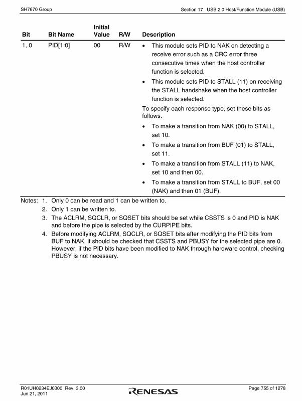
Section 17 USB 2.0 Host/Function Module (USB)
R01UH0234EJ0300 Rev. 3.00 Page 755 of 1278 Jun 21, 2011
SH7670 Group
Bit Bit Name Initial Value R/W Description
1, 0 PID[1:0] 00 R/W • This module sets PID to NAK on detecting a
receive error such as a CRC error three
consecutive times when the host controller
function is selected.
• This module sets PID to STALL (11) on receiving
the STALL handshake when the host controller
function is selected.
To specify each response type, set these bits as follows.
• To make a transition from NAK (00) to STALL,
set 10.
• To make a transition from BUF (01) to STALL,
set 11.
• To make a transition from STALL (11) to NAK,
set 10 and then 00.
• To make a transition from STALL to BUF, set 00
(NAK) and then 01 (BUF).
Notes: 1. Only 0 can be read and 1 can be written to.
2. Only 1 can be written to. 3. The ACLRM, SQCLR, or SQSET bits should be set while CSSTS is 0 and PID is NAK
and before the pipe is selected by the CURPIPE bits. 4. Before modifying ACLRM, SQCLR, or SQSET bits after modifying the PID bits from
BUF to NAK, it should be checked that CSSTS and PBUSY for the selected pipe are 0. However, if the PID bits have been modified to NAK through hardware control, checking PBUSY is not necessary.

Section 17 USB 2.0 Host/Function Module (USB)
Page 756 of 1278 R01UH0234EJ0300 Rev. 3.00 Jun 21, 2011
SH7670 Group
Table 17.15 Information Cleared by this Module by Setting ACLRM = 1
No. Information Cleared by ACLRM Bit Manipulation
Cases in which Clearing the Information is Necessary
1 All the information in the FIFO buffer assigned to the pertinent pipe
2 When the host controller function is selected, the interval count value when the pertinent pipe is for isochronous transfer
When the interval count value is to be reset
3 Values of the internal flags related to the BFRE bit
When the BFRE setting is modified
4 Values of the internal flags related to the transaction count
When the transaction count function is forcibly terminated
17.3.37 PIPEn Transaction Counter Enable Registers (PIPEnTRE) (n = 1 to 5)
PIPEnTRE is a register that enables or disables the transaction counter corresponding to PIPE1 to PIPE5, and clears the transaction counter.
This register is initialized by a power-on reset.
15 14 13 12 11 10 9 8 7 6 5 4 3 2 1 0Bit:
Initial value:R/W:
0 0 0 0 0 0 0 0 0 0 0 0 0 0 0 0R R R R R R/W R/WR R R R R R R R R
— — — — — — TRENB TRCLR — — — — — — ——
Bit Bit Name Initial Value R/W Description
15 to 10 ⎯ All 0 R Reserved
These bits are always read as 0. The write value should always be 0.
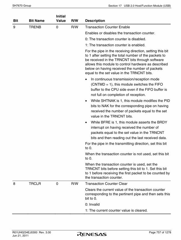
Section 17 USB 2.0 Host/Function Module (USB)
R01UH0234EJ0300 Rev. 3.00 Page 757 of 1278 Jun 21, 2011
SH7670 Group
Bit Bit Name Initial Value R/W Description
9 TRENB 0 R/W Transaction Counter Enable
Enables or disables the transaction counter.
0: The transaction counter is disabled.
1: The transaction counter is enabled.
For the pipe in the receiving direction, setting this bit to 1 after setting the total number of the packets to be received in the TRNCNT bits through software allows this module to control hardware as described below on having received the number of packets equal to the set value in the TRNCNT bits.
• In continuous transmission/reception mode
(CNTMD = 1), this module switches the FIFO buffer to the CPU side even if the FIFO buffer is
not full on completion of reception.
• While SHTNAK is 1, this module modifies the PID
bits to NAK for the corresponding pipe on having received the number of packets equal to the set
value in the TRNCNT bits.
• While BFRE is 1, this module asserts the BRDY
interrupt on having received the number of packets equal to the set value in the TRNCNT
bits and then reading out the last received data.
For the pipe in the transmitting direction, set this bit to 0.
When the transaction counter is not used, set this bit to 0.
When the transaction counter is used, set the TRNCNT bits before setting this bit to 1. Set this bit to 1 before receiving the first packet to be counted by the transaction counter.
8 TRCLR 0 R/W Transaction Counter Clear
Clears the current value of the transaction counter corresponding to the pertinent pipe and then sets this bit to 0.
0: Invalid
1: The current counter value is cleared.
Section 17 USB 2.0 Host/Function Module (USB)
Page 758 of 1278 R01UH0234EJ0300 Rev. 3.00 Jun 21, 2011
SH7670 Group
Bit Bit Name Initial Value R/W Description
7 to 0 ⎯ All 0 R Reserved
These bits are always read as 0. The write value should always be 0.
Note: Modify each bit in this register while CSSTS is 0 and PID is NAK. Before modifying each bit after modifying the PID bits for the corresponding pipe from BUF to NAK, check that CSSTS and PBUSY are 0. However, if the PID bits have been modified to NAK by this module, checking PBUSY through software is not necessary.
17.3.38 PIPEn Transaction Counter Registers (PIPEnTRN) (n = 1 to 5)
PIPEnTRN is a transaction counter corresponding to PIPE1 to PIPE5.
This register is initialized by a power-on reset, but retains the set value by a USB bus reset.
15 14 13 12 11 10 9 8 7 6 5 4 3 2 1 0Bit:
Initial value:R/W:
0 0 0 0 0 0 0 0 0 0 0 0 0 0 0 0R/W R/W R/W R/W R/W R/W R/W R/W R/W R/W R/W R/W R/W R/W R/W R/W
TRNCNT[15:0]
Bit Bit Name Initial Value R/W Description
15 to 0 TRNCNT[15:0] All 0 R/W Transaction Counter
When written to:
Specifies the number of transactions to be transferred through DMA.
When read from:
Indicates the specified number of transactions if TRENB is 0.
Indicates the number of the currently counted transaction if TRENB is 1.

Section 17 USB 2.0 Host/Function Module (USB)
R01UH0234EJ0300 Rev. 3.00 Page 759 of 1278 Jun 21, 2011
SH7670 Group
Bit Bit Name Initial Value R/W Description
15 to 0 TRNCNT[15:0] All 0 R/W This module increments the value of these bits by one when all of the following conditions are satisfied on receiving the packet.
• TRENB is 1.
• (TRNCNT set value ≠ current counter value + 1)
on receiving the packet.
• The payload of the received packet agrees with
the set value in the MXPS bits.
This module clears the value of these bits to 0 when any of the following conditions are satisfied.
• All the following conditions are satisfied.
TRENB is 1.
(TRNCNT set value = current counter value + 1) on receiving the packet.
The payload of the received packet agrees with the set value in the MXPS bits.
• All the following conditions are satisfied.
TRENB is 1.
This module has received a short packet.
• All the following conditions are satisfied.
TRENB is 1.
Software has set the TRCLR bit to 1.
For the pipe in the transmitting direction, set these bits to 0.
When the transaction counter is not used, set these bits to 0.
Modify these bits while CSSTS is 0, PID is NAK, and TRENB is 0.
Before modifying these bits after modifying the PID bits for the corresponding pipe from BUF to NAK, check that CSSTS and PBUSY are 0. However, if the PID bits have been modified to NAK by this module, checking PBUSY through software is not necessary.
To modify the value of these bits, set TRNCNT to 1 before setting TRENB to 1.

Section 17 USB 2.0 Host/Function Module (USB)
Page 760 of 1278 R01UH0234EJ0300 Rev. 3.00 Jun 21, 2011
SH7670 Group
17.3.39 Device Address n Configuration Registers (DEVADDn) (n = 0 to A)
DEVADDn is a register that specifies the address and port number of the hub to which the communication target peripheral device is connected and that also specifies the transfer speed of the peripheral device for PIPE0 to PIPEA.
When the host controller function is selected, this register should be set before starting communication using each pipe.
The bits in this register should be modified while no valid pipes are using the settings of this register. Valid pipes refer to the ones satisfying both of condition 1 and 2 below.
1. This register is selected by the DEVSEL bits as the communication target.
2. The PID bits are set to BUF for the selected pipe or the selected pipe is the DCP with SUREQ being 1.
This register is initialized by a power-on reset.
15 14 13 12 11 10 9 8 7 6 5 4 3 2 1 0Bit:
Initial value:R/W:
0 0 0 0 0 0 0 0 0 0 0 0 0 0 0 0R R/W R/W R/W R/W R/W R/WR/W R/W R/W R R R R R R
— UPPHUB[3:0] HUBPORT[2:0] USBSPD[1:0] — — — — ——
Bit Bit Name Initial Value R/W Description
15 ⎯ 0 R Reserved
This bit is always read as 0. The write value should always be 0.

Section 17 USB 2.0 Host/Function Module (USB)
R01UH0234EJ0300 Rev. 3.00 Page 761 of 1278 Jun 21, 2011
SH7670 Group
Bit Bit Name Initial Value R/W Description
14 to 11 UPPHUB[3:0] 0000 R/W Address of Hub to which Communication Target is Connected
Specifies the USB address of the hub to which the communication target peripheral device is connected.
0000: The peripheral device is directly connected to the port of this LSI.
0001 to 1010: USB address of the hub
1011 to 1111: Setting prohibited
When the host controller function is selected, this module refers to the setting of these bits to generate packets for split transactions.
When the function controller function is selected, set these bits to 0000.
10 to 8 HUBPORT[2:0] 000 R/W Port Number of Hub to which Communication Target is Connected
Specifies the port number of the hub to which the communication target peripheral device is connected.
000: The peripheral device is directly connected to the port of this LSI.
001 to 111: Port number of the hub
When the host controller function is selected, this module refers to the setting of these bits to generate packets for split transactions.
When the function controller function is selected, set these bits to 000.
Section 17 USB 2.0 Host/Function Module (USB)
Page 762 of 1278 R01UH0234EJ0300 Rev. 3.00 Jun 21, 2011
SH7670 Group
Bit Bit Name Initial Value R/W Description
7, 6 USBSPD[1:0] 00 R/W Transfer Speed of the Communication Target Device
Specifies the USB transfer speed of the communication target peripheral device.
00: DEVADDn is not used.
01: Low speed
10: Full speed
11: High speed
When the host controller function is selected, this module refers to the setting of these bits to generate packets.
When the function controller function is selected, set these bits to 00.
5 to 0 ⎯ All 0 R Reserved
These bits are always read as 0. The write value should always be 0.

Section 17 USB 2.0 Host/Function Module (USB)
R01UH0234EJ0300 Rev. 3.00 Page 763 of 1278 Jun 21, 2011
SH7670 Group
17.3.40 Bus Wait Register (D0FWAIT, D1FWAIT)
D0FWAIT and D1FWAIT each specify the number of access waits for those registers of this module that are connected to the internal bus (that is, D0FWAIT, D1FWAIT, D0FIFO, and D1FIFO). The basic clock for this module is a USB clock of 48 MHz, and access from the internal bus is performed through Bφ synchronization. For this reason, the USB clock must be multiplied by a certain number of cycles when accessing registers of this module via the internal bus. The number of access waits should be adjusted to produce at least the approximate value shown below: 83.4 ns (USB clock × 4 cycles) when the size of access is 32 bits, 41.7 ns (USB clock × 2 cycles) when the size of access is 16 bits, or 20.8 ns (USB clock × 1 cycle) when the size of access is 8 bits.
15 14 13 12 11 10 9 8 7 6 5 4 3 2 1 0Bit:
Initial Value:R/W:
0 0 0 0 0 0 0 0 0 0 0 1 1R R R R R R R R R R R R R/W R/W R/W R/W
0
— — — — — — — — — — ——
1 1
BWAIT[3:0]
Bit Bit Name Initial Value R/W Description
15 to 4 ⎯ All 0 R Reserved
These bits are always read as 0. The write value should always be 0.
3 to 0 BWAIT[3:0] 1111 R/W Bus Wait between DMAC and FIFO
On a Bφ basis, set the number of waits needed when accessing registers of this module via the internal bus.
0000: 0 wait (accessing two cycles on a Bφ basis)
0001: 1 wait (accessing three cycles on a Bφ basis)
0010: 2 waits (accessing four cycles on a Bφ basis)
:
1111: 15 waits (accessing 17 cycles on a Bφ basis)
Note: Be sure to set this bit in the initialization routine of this module by taking into account the Bφ and access size.
Section 17 USB 2.0 Host/Function Module (USB)
Page 764 of 1278 R01UH0234EJ0300 Rev. 3.00 Jun 21, 2011
SH7670 Group
17.4 Operation
17.4.1 System Control and Oscillation Control
This section describes the register operations that are necessary to the initial settings of this module, and the registers necessary for power consumption control.
(1) Resets
Table 17.16 lists the types of controller resets. For the initialized states of the registers following the reset operations, see section 17.3, Register Description.
Table 17.16 Types of Reset
Name Operation
Power-on reset Low level input from the RES pin
USB bus reset Automatically detected by this module from the D+ and D− lines when the function controller function is selected
(2) Controller Function Selection
This module can select the host controller function or function controller function using the DCFM bit in SYSCFG. Changing the DCFM bit should be done in the initial settings immediately after a power-on reset or in the D+ pull-up disabled (DPRPU = 0) and D + /D − pull-down disabled (DRPD = 0) state.
(3) Enabling High-Speed Operation
This module can select a USB communication speed (communication bit rate) using software. When the host controller function is selected, either of the high-speed operation or full-speed/low-speed operation can be selected. In order to enable the high-speed operation for this module, the HSE bit in SYSCFG should be set to 1. If high-speed mode has been enabled, this module executes the reset handshake protocol, and the USB communication speed is set automatically. The results of the reset handshake can be confirmed using the RHST bit in DVSTCTR.
If high-speed operation has been disabled, this module operates at full-speed or low-speed. If the function controller function is also selected, this module operates at full-speed.
Changing the HSE bit should be done between the ATTCH interrupt detection and bus reset execution when the host controller function is selected, or with the D+ line pull-up disabled (DPRPU = 0) when the host controller function is selected.
Section 17 USB 2.0 Host/Function Module (USB)
R01UH0234EJ0300 Rev. 3.00 Page 765 of 1278 Jun 21, 2011
SH7670 Group
(4) USB Data Bus Resistor Control
Figure 17.1 shows a diagram of the connections between this module and the USB connectors.
This module incorporates a pull-up resistor for the D+ signal and a pull-down resistor for the D+ and D- signals. These signals can be pulled up or down using the DPRPU and DRPD bits in SYSCFG.
This module controls the terminal resistor for the D+ and D- signals during high-speed operation and the output resistor for the signals during full-speed operation. This module automatically switches the resistor after connection with the host controller or peripheral device by means of reset handshake, suspended state and resume detection.
When the function controller function is selected and the DPRPU bit in SYSCFG is cleared to 0 during communication with the host controller, the pull-up resistor (or the terminal resistor) of the USB data line is disabled, making it possible to notify the USB host of the device disconnection.

Section 17 USB 2.0 Host/Function Module (USB)
Page 766 of 1278 R01UH0234EJ0300 Rev. 3.00 Jun 21, 2011
SH7670 Group
Legend
This LSI
: Output impedance: Pull-down resistor: Pull-up resistor
D-
D+
USBconnector
DP
DM
ZPD
ZDRU
ZDRUZPDZPU
ZPU
ZPD
ZDRU
Figure 17.1 UBS Connector Connection

Section 17 USB 2.0 Host/Function Module (USB)
R01UH0234EJ0300 Rev. 3.00 Page 767 of 1278 Jun 21, 2011
SH7670 Group
17.4.2 Interrupt Functions
Table 17.17 lists the interrupt generation conditions for this module.
When an interrupt generation condition is satisfied and the interrupt output is enabled using the corresponding interrupt enable register, this module issues a USB interrupt request to the INTC.
Table 17.17 Interrupt Generation Conditions
Bit Interrupt Name Cause of Interrupt
Function That Generates the Interrupt
Related Status
VBINT VBUS interrupt When a change in the state of the VBUS input pin has been detected (low to high or high to low)
Host,
function
VBSTS
RESM Resume interrupt When a change in the state of the USB bus has been detected in the suspended state
(J-state to K-state or J-state to SE0)
Function ⎯
SOFR Frame number update interrupt
When the host controller function is selected:
• When an SOF packet with a different frame number has been
transmitted
When the function controller function is selected:
• SOFRM = 0:
When an SOF packet with a different frame number is received
• SOFRM = 1:
When the SOF with the μframe number 0 cannot be received due to a corruption of a packet
Host,
function
⎯
DVST Device state transition interrupt
When a device state transition is detected
• A USB bus reset detected
• The suspend state detected
• SET_ADDRESS request received
• SET_CONFIGURATION request
received
Function DVSQ

Section 17 USB 2.0 Host/Function Module (USB)
Page 768 of 1278 R01UH0234EJ0300 Rev. 3.00 Jun 21, 2011
SH7670 Group
Bit Interrupt Name Cause of Interrupt
Function That Generates the Interrupt
Related Status
CTRT Control transfer stage transition interrupt
When a stage transition is detected in control transfer
• Setup stage completed
• Control write transfer status stage
transition
• Control read transfer status stage
transition
• Control transfer completed
• A control transfer sequence error
occurred
Function CTSQ
BEMP Buffer empty interrupt
• When transmission of all of the data in the buffer memory has
been completed
• When an excessive maximum
packet size error has been
detected
Host,
Function
BEMPSTS.PIPEBEMP
NRDY Buffer not ready interrupt
When the host controller function is selected:
• When STALL is received from the peripheral side for the issued token
• When a response cannot be received correctly from the peripheral side for the issued token (No response is returned three consecutive times or a packet reception error occurred three consecutive times.)
• When an overrun/underrun occurred during isochronous transfer
Host, function NRDYSTS.PIPENRDY

Section 17 USB 2.0 Host/Function Module (USB)
R01UH0234EJ0300 Rev. 3.00 Page 769 of 1278 Jun 21, 2011
SH7670 Group
Bit Interrupt Name Cause of Interrupt
Function That Generates the Interrupt
Related Status
NRDY Buffer not ready interrupt
When the function controller function is selected:
• When NAK is returned for an IN/OUT/PING token.
• When a CRC error or a bit stuffing error occurred during data reception in isochronous transfer
• When an overrun/underrun occurred during data reception in isochronous transfer
Host, function NRDYSTS.PIPENRDY
BRDY Buffer ready interrupt
When the buffer is ready (reading or writing is enabled)
Host, function BRDYSYS PIPEBRDY
BCHG Bus change interrupt
When a change of USB bus state is detected
Host, function ⎯
DTCH Disconnection detection during full-speed operation
When disconnection of a peripheral device during full-speed operation is detected
Host ⎯
ATTCH Device connection detection
When J-state or K-state is detected on the USB port for 2.5 μs.
Used for checking whether a peripheral device is connected.
Host ⎯
EOFERR EOF error detection
When EOF error of a peripheral device is detected
Host ⎯
SACK Normal setup operation
When the normal response (ACK) for the setup transaction is received
Host ⎯
SIGN Setup error When a setup transaction error (no response or ACK packet corruption) is detected three consecutive times.
Host ⎯
Note: All the bits without register name indication are in INTSTS0.

Section 17 USB 2.0 Host/Function Module (USB)
Page 770 of 1278 R01UH0234EJ0300 Rev. 3.00 Jun 21, 2011
SH7670 Group
Figure 17.2 shows a diagram relating to interrupts of this module.
USB bus reset detected
Set_Address detected
Set_Configuration detected
Suspended state detected
BEMP interrupt enable register
Control write data stage
Control read data stage
Completion of control transfer
Control transfer setup reception
Control transfer error
VBSE
INTENB0 INTSTS0
RSME
SOFE
DVSE
CTRE
BEMPE
NRDYE
BRDYE
VBINT
RESM
SOFR
DVST
BCHGE
INTENB1 INTSTS1
DTCHE
SIGNE
SACKE
BCHG
DTCH
ATTCHE
EOFERRE
ATTCH
EOFERR
SIGN
SACK
CTRT
BEMP
NRDY
BRDY
::
b9 ... b1 b0
b9
b1
b0
BE
MP
inte
rrup
tst
atus
reg
iste
r
NRDY interrupt enable register
::
b9 ... b1 b0
b9
b1
b0
NR
DY
inte
rrup
tst
atus
reg
iste
r
BRDY interrupt enable register
::
b9 ... b1 b0
b9
b1
b0
BR
DY
inte
rrup
tst
atus
reg
iste
r
Generationcircuit
Interruptrequest
...
...
...
Figure 17.2 Items Relating to Interrupts

Section 17 USB 2.0 Host/Function Module (USB)
R01UH0234EJ0300 Rev. 3.00 Page 771 of 1278 Jun 21, 2011
SH7670 Group
(1) BRDY Interrupt
The BRDY interrupt is generated when either of the host controller function or function controller function is selected. The following shows the conditions under which this module sets 1 to a corresponding bit in BRDYSTS. Under this condition, this module generates BRDY interrupt, if software sets the PIPEBRDYE bit in BRDYENB that corresponds to the pipe to 1 and the BRDYE bit in INTENB0 to 1.
The conditions for generating and clearing the BRDY interrupt depend on the settings of the BRDYM bit and BFRE bit for the pertinent pipe as described below.
(a) When the BRDYM bit is 0 and BFRE bit is 0
With these settings, the BRDY interrupt indicates that the FIFO port is accessible.
On any of the following conditions, this module generates the internal BRDY interrupt request trigger and sets 1 to the PIPEBRDY bit corresponding to the pertinent pipe.
(i) For the pipe in the transmitting direction:
⎯ When software changes the DIR bit from 0 to 1.
⎯ When packet transmission is completed using the pertinent pipe when write-access from the CPU to the FIFO buffer for the pertinent pipe is disabled (when the BSTS bit is read as 0).
⎯ In continuous transmission/reception mode, the request trigger is generated on completion of transmitting data of one plane of the FIFO buffer.
⎯ When one FIFO buffer is empty on completion of writing data to the other FIFO buffer in double buffer mode.
⎯ The request trigger is not generated until completion of writing data to the currently-written FIFO buffer plane even if transmission to the other FIFO buffer is completed.
⎯ When the hardware flushes the buffer of the pipe for isochronous transfers.
⎯ When 1 is written to the ACLRM bit, which causes the FIFO buffer to make transition from the write-disabled to write-enabled state.
The request trigger is not generated for the DCP (that is, during data transmission for control transfers).

Section 17 USB 2.0 Host/Function Module (USB)
Page 772 of 1278 R01UH0234EJ0300 Rev. 3.00 Jun 21, 2011
SH7670 Group
(ii) For the pipe in the receiving direction:
⎯ When packet reception is completed successfully thus enabling the FIFO buffer to be read when read-access from the CPU to the FIFO buffer for the pertinent pipe is disabled (when the BSTS bit is read as 0).
The request trigger is not generated for the transaction in which DATA-PID disagreement occurs.
In continuous transmission/reception mode, the request trigger is not generated when the data is of the specified maximum packet size and the buffer has available space.
When a short packet is received, the request trigger is generated even if the FIFO buffer has available space.
When the transaction counter is used, the request trigger is generated on receiving the specified number of packets. In this case, the request trigger is generated even if the FIFO buffer has available space.
⎯ When one FIFO buffer is read-enabled on completion of reading data from the other FIFO buffer in double buffer mode.
The request trigger is not generated until completion of reading data from the currently-read FIFO buffer plane even if reception by the other FIFO buffer is completed.
When the function controller function is selected, the BRDY interrupt is not generated in the status stage of control transfers. The PIPEBRDY interrupt status of the pertinent pipe can be cleared to 0 by writing 0 to the corresponding PIPEBRDY interrupt status bit in the BRDYSTS register through software. In this case, 1s should be written to the PIPEBRDY interrupt status bits for the other pipes. Be sure to clear the BRDY status before accessing the FIFO buffer.
Section 17 USB 2.0 Host/Function Module (USB)
R01UH0234EJ0300 Rev. 3.00 Page 773 of 1278 Jun 21, 2011
SH7670 Group
(b) When the BRDYM bit is 0 and the BFRE bit is 1
With these settings, this module generates the BRDY interrupt on completion of reading all the data for a single transfer using the pipe in the receiving direction, and sets 1 to the PIPEBRDY bit corresponding to the pertinent pipe.
On any of the following conditions, this module determines that the last data for a single transfer has been received.
• When a short packet including a zero-length packet is received.
• When the transaction counter register (TRNCNT bits) is used and the number of packets specified by the TRNCNT bits are completely received.
When the pertinent data is completely read out after any of the above determination conditions has been satisfied, this module determines that all the data for a single transfer has been completely read out.
When a zero-length packet is received when the FIFO buffer is empty, this module determines that all the data for a single transfer has been completely read out upon passing the zero-length packet data to the CPU. In this case, to start the next transfer, write 1 to the BCLR bit in the corresponding FIFOCTR register through software.
With these settings, this module does not detect the BRDY interrupt for the pipe in the transmitting direction.
The PIPEBRDY interrupt status of the pertinent pipe can be cleared to 0 by writing 0 to the corresponding PIPEBRDY interrupt status bit through software. In this case, 1s should be written to the PIPEBRDY interrupt status bits for the other pipes.
In this mode, the BFRE bit setting should not be modified until all the data for a single transfer has been processed. When it is necessary to modify the BFRE bit before completion of processing, all the FIFO buffers for the pertinent pipe should be cleared using the ACLRM bit.

Section 17 USB 2.0 Host/Function Module (USB)
Page 774 of 1278 R01UH0234EJ0300 Rev. 3.00 Jun 21, 2011
SH7670 Group
(c) When the BRDYM bit is 1 and the BFRE bit is 0
With these settings, the PIPEBRDY values are linked to the BSTS bit settings for each pipe. In other words, the BRDY interrupt status bits (PIPEBRDY) are set to 1 or 0 by this module depending on the FIFO buffer status.
(i) For the pipe in the transmitting direction:
The BRDY interrupt status bits are set to 1 when the FIFO buffer is write-enabled and are set to 0 when write-disabled. However, the BRDY interrupt is not generated if the DCP in the transmitting direction is write-enabled.
(ii) For the pipe in the receiving direction:
The BRDY interrupt status bits are set to 1 when the FIFO buffer is read-enabled and are set to 0 when all the data have been read (read-disabled). When a zero-length packet is received when the FIFO buffer is empty, the pertinent bit is set to 1 and the BRDY interrupt is continuously generated until BCLR = 1 is written through software. With this setting, the PIPEBRDY bit cannot be cleared to 0 through software. When BRDYM is set to 1, all of the BFRE bits (for all pipes) should be cleared to 0.
Figure 17.3 shows the timing at which the BRDY interrupt is generated.

Section 17 USB 2.0 Host/Function Module (USB)
R01UH0234EJ0300 Rev. 3.00 Page 775 of 1278 Jun 21, 2011
SH7670 Group
Token packet
Token packet
Token packet
ACK handshake
ACK handshake
ACK handshakeData packet
Buffer read
Buffer write
Zero-length packet/short data packet/data packet (full)
(transaction count)
Short data packet/data packet
(transaction count)
A BRDY interrupt is generatedbecause reading from the bufferis enabled.
A BRDY interrupt is generatedbecause the transfer has ended.
A BRDY interrupt is generatedbecause writing to the buffer is enabled.
(1) Zero-length packet reception or data packet reception when BFRE = 0 (short packet reception/transaction counter completion/buffer full)
(2) Data packet reception when BFRE = 1 (short packet reception/transaction counter completion)
(3) Packet transmission
USB bus
USB bus
USB bus
BRDY interrupt
BRDY interrupt
BRDY interrupt
Figure 17.3 Timing at which a BRDY Interrupt is Generated

Section 17 USB 2.0 Host/Function Module (USB)
Page 776 of 1278 R01UH0234EJ0300 Rev. 3.00 Jun 21, 2011
SH7670 Group
(2) NRDY Interrupt
On generating the internal NRDY interrupt request for the pipe whose PID bits are set to BUF by software, this module sets the corresponding PIPENRDY bit in NRDYSTS to 1. If the corresponding bit in NRDYENB is set to 1 by software, this module sets the NRDY bit in INTSTS0 to 1, allowing the USB interrupt to be generated.
The following describes the conditions on which this module generates the internal NRDY interrupt request for a given pipe.
However, the internal NRDY interrupt request is not generated during setup transaction execution when the host controller function is selected. During setup transactions when the host controller function is selected, the SACK or SIGN interrupt is detected.
The internal NRDY interrupt request is not generated during status stage execution of the control transfer when the function controller function is selected.
(a) When the host controller function is selected and when the connection is used in which no split transactions occur
(i) For the pipe in the transmitting direction:
On any of the following conditions, this module detects the NRDY interrupt.
⎯ For the pipe for isochronous transfers, when the time to issue an OUT token comes in a state in which there is no data to be transmitted in the FIFO buffer.
In this case, this module transmits a zero-length packet following the OUT token, setting the corresponding PIPENRDY bit and the OVRN bit to 1.
⎯ During communications other than setup transactions using the pipe for the transfers other than isochronous transfers, when any combination of the following two cases occur three consecutive times: 1) no response is returned from the peripheral device (when timeout is detected before detection of the handshake packet from the peripheral device) and 2) an error is detected in the packet from the peripheral device.
In this case, this module sets the corresponding PIPENRDY bit to 1 and modifies the setting of the PID bits of the corresponding pipe to NAK.
⎯ During communications other than setup transactions, when the STALL handshake is received from the peripheral device (including the STALL handshake in response to PING in addition to the STALL handshake in response to OUT).
In this case, this module sets the corresponding PIPENRDY bit to 1 and modifies the setting of the PID bits of the corresponding pipe to STALL (11).

Section 17 USB 2.0 Host/Function Module (USB)
R01UH0234EJ0300 Rev. 3.00 Page 777 of 1278 Jun 21, 2011
SH7670 Group
(ii) For the pipe in the receiving direction
⎯ For the pipe for isochronous transfers, when the time to issue an IN token comes in a state in which there is no space available in the FIFO buffer.
In this case, this module discards the received data for the IN token, setting the PIPENRDY bit of the corresponding pipe and the OVRN bit to 1.
When a packet error is detected in the received data for the IN token, this module also sets the CRCE bit to 1.
⎯ For the pipe for the transfers other than isochronous transfers, when any combination of the following two cases occur three consecutive times: 1) no response is returned from the peripheral device for the IN token issued by this module (when timeout is detected before detection of the DATA packet from the peripheral device) and 2) an error is detected in the packet from the peripheral device.
In this case, this module sets the corresponding PIPENRDY bit to 1 and modifies the setting of the PID bits of the corresponding pipe to NAK.
⎯ For the pipe for isochronous transfers, when no response is returned from the peripheral device for the IN token (when timeout is detected before detection of the DATA packet from the peripheral device) or an error is detected in the packet from the peripheral device.
In this case, this module sets the corresponding PIPENRDY bit to 1. (The setting of the PID bits of the corresponding pipe to NAK is not modified.)
⎯ For the pipe for isochronous transfers, when a CRC error or a bit stuffing error is detected in the received data packet.
In this case, this module sets the corresponding PIPENRDY bit and CRCE bit to 1.
⎯ When the STALL handshake is received.
In this case, this module sets the corresponding PIPENRDY bit to 1 and modifies the setting of the PID bits of the corresponding pipe to STALL.
Section 17 USB 2.0 Host/Function Module (USB)
Page 778 of 1278 R01UH0234EJ0300 Rev. 3.00 Jun 21, 2011
SH7670 Group
(b) When the host controller function is selected and when the connection is used in which split transactions occur
(i) For the pipe in the transmitting direction:
⎯ For the pipe for isochronous transfers, when the time to issue an OUT token comes in a state in which there is no data to be transmitted in the FIFO buffer.
In this case, this module transmits a zero-length packet following the OUT token, setting the corresponding PIPENRDY bit and the OVRN bit to 1 at the issuance of the start-split transaction (S-SPLIT).
⎯ For the pipe for the transfers other than isochronous transfers, when any combination of the following two cases occur three consecutive times: 1) no response is returned from the HUB for the S-SPLIT or complete-split transaction (C-SPLIT) (when timeout is detected before detection of the handshake packet from the HUB) and 2) an error is detected in the packet from the HUB.
In this case, this module sets the PIPENRDY bit of the corresponding pipe to 1 and modifies the setting of the PID bits of the corresponding pipe to NAK.
If the NRDY interrupt is detected when the C-SPLIT is issued, this module clears the CSSTS bit to 0.
⎯ When the STALL handshake is received in response to the C-SPLIT.
In this case, this module sets the corresponding PIPENRDY bit to 1, modifies the setting of the PID bits of the corresponding pipe to STALL (11) and clears the CSSTS bit to 0.
This interrupt is not detected for SETUP transactions.
⎯ When the NYET is received in response to the C-SPLIT and the microframe number = 4.
In this case, this module sets the corresponding PIPENRDY bit to 1 and clears the CSSTS bit to 0 (does not modify the setting of the PID bits).

Section 17 USB 2.0 Host/Function Module (USB)
R01UH0234EJ0300 Rev. 3.00 Page 779 of 1278 Jun 21, 2011
SH7670 Group
(ii) For the pipe in the receiving direction:
⎯ For the pipe for isochronous transfers, when the time to issue an IN token comes in a state in which there is no space available in the FIFO buffer.
In this case, this module discards the received data for the IN token, setting the corresponding PIPENRDY bit and the OVRN bit to 1 at the issuance of the S-SPLIT.
⎯ During bulk-pipe transfers or the transfers other than SETUP transactions with the DCP, when any combination of the following two cases occur three consecutive times: 1) no response is returned from the HUB for the IN token issued by this module at the issuance of S-SPLIT or C-SPLIT (when timeout is detected before detection of the DATA packet from the HUB) and 2) an error is detected in the packet from the HUB.
In this case, this module sets the corresponding PIPENRDY bit to 1 and modifies the setting of the PID bits of the corresponding pipe to NAK. When the condition is generated during the C-SPLIT transaction, this module clears the CSSTS bit to 0.
⎯ During the C-SPLIT transaction for the pipe for isochronous transfers or interrupt transfers, when any combination of the following two cases occur three consecutive times: 1) no response is returned from the HUB for the IN token issued by this module (when timeout is detected before detection of the DATA packet from the HUB) and 2) an error is detected in the packet from the HUB.
On generating this condition for the pipe for interrupt transfers, this module sets the corresponding PIPENRDY bit to 1, modifies the setting of the PID bits of the corresponding pipe to NAK and clears the CSSTS bit to 0.
On generating this condition for the pipe for isochronous transfers, this module sets the corresponding PIPENRDY bit to 1 and CRCE bit to 1, and clears the CSSTS bit to 0 (does not modify the setting of the PID bits).
⎯ During the C-SPLIT transaction, when the STALL handshake is received for the pipe for the transfers other than isochronous transfers.
In this case, this module sets the corresponding PIPENRDY bit to 1, modifies the setting of the PID bits of the corresponding pipe to STALL (11) and clears the CSSTS bit to 0.
⎯ During the C-SPLIT transaction, when the NYET handshake is received for the pipe for the isochronous transfers or interrupt transfers and the microframe number = 4.
In this case, this module sets the corresponding PIPENRDY bit to 1 and CRCE bit to 1, and clears the CSSTS bit to 0 (does not modify the setting of the PID bits).

Section 17 USB 2.0 Host/Function Module (USB)
Page 780 of 1278 R01UH0234EJ0300 Rev. 3.00 Jun 21, 2011
SH7670 Group
(c) When the function controller function is selected
(i) For the pipe in the transmitting direction:
⎯ On receiving an IN token when there is no data to be transmitted in the FIFO buffer.
In this case, this module generates a NRDY interrupt request at the reception of the IN token, setting the PIPENRDY bit to 1. For the pipe for the isochronous transfers in which an interrupt is generated, this module transmits a zero-length packet, setting the OVRN bit to 1.
(ii) For the pipe in the receiving direction:
⎯ On receiving an OUT token when there is no space available in the FIFO buffer.
For the pipe for the isochronous transfers in which an interrupt is generated, this module generates a NRDY interrupt request, setting the PIPENRDY bit to 1 and OVRN bit to 1.
For the pipe for the transfers other than isochronous transfers in which an interrupt is generated, this module generates a NRDY interrupt request when a NAK handshake is transferred after the data following the OUT token was received, setting the PIPENRDY bit to 1.
However, during re-transmission (due to DATA-PID disagreement), the NRDY interrupt request is not generated. In addition, if an error occurs in the DATA packet, the NRDY interrupt request is not generated.
⎯ On receiving a PING token when there is no space available in the FIFO buffer.
In this case, this module generates a NRDY interrupt request at the reception of the PING token, setting the PIPENRDY bit to 1.
⎯ For the pipe for isochronous transfers, when a token is not received normally within an interval frame.
In this case, this module generates a NRDY interrupt request, setting the PIPENRDY bit to 1.

Section 17 USB 2.0 Host/Function Module (USB)
R01UH0234EJ0300 Rev. 3.00 Page 781 of 1278 Jun 21, 2011
SH7670 Group
Figure 17.4 shows the timing at which an NRDY interrupt is generated when the function controller function is selected.
IN token packet
NAK handshake
NAK handshake
NAK handshakeOUT token packet Data packet
PING packet
(1) Data transmission
(2) Data reception: OUT token reception
(3) Data reception: PING token reception
USB bus
NRDY interrupt
USB bus
NRDY interrupt
(CRC error, etc)
USB bus
NRDY interrupt
Figure 17.4 Timing at which NRDY Interrupt is Generated when Function Controller Function is Selected
Section 17 USB 2.0 Host/Function Module (USB)
Page 782 of 1278 R01UH0234EJ0300 Rev. 3.00 Jun 21, 2011
SH7670 Group
(3) BEMP Interrupt
On generating the BEMP interrupt for the pipe whose PID bits are set to BUF by software, this module sets the corresponding PIPEBEMP bit in BEMPSTS to 1. If the corresponding bit in BEMPENB is set to 1 by software, this module sets the BEMP bit in INTSTS0 to 1, allowing the USB interrupt to be generated.
The following describes the conditions on which this module generates the internal BEMP interrupt request.
(a) For the pipe in the transmitting direction, when the FIFO buffer of the corresponding pipe is empty on completion of transmission (including zero-length packet transmission). In single buffer mode, the internal BEMP interrupt request is generated simultaneously with the BRDY interrupt for the pipe other than DCP. However, the internal BEMP interrupt request is not generated on any of the following conditions.
⎯ When software (DMAC) has already started writing data to the FIFO buffer of the CPU on completion of transmitting data of one plane in double buffer mode.
⎯ When the buffer is cleared (emptied) by setting the ACLRM or BCLR bit to 1.
⎯ When IN transfer (zero-length packet transmission) is performed during the control transfer status stage in function controller mode.
(b) For the pipe in the receiving direction: When the successfully-received data packet size exceeds the specified maximum packet size. In this case, this module generates the BEMP interrupt request, setting the corresponding PIPEBEMP bit to 1, and discards the received data and modifies the setting of the PID bits of the corresponding pipe to STALL (11). Here, this module returns no response when used as the host controller, and returns STALL response when used as the function controller. However, the internal BEMP interrupt request is not generated on any of the following conditions.
⎯ When a CRC error or bit stuffing error is detected in the received data.
⎯ When a setup transaction is being performed. Writing 0 to the PIPEBEMP bit clears the status; writing 1 to the PIPEBEMP bit has no effect.

Section 17 USB 2.0 Host/Function Module (USB)
R01UH0234EJ0300 Rev. 3.00 Page 783 of 1278 Jun 21, 2011
SH7670 Group
Figure 17.5 shows the timing at which a BEMP interrupt is generated when the function controller function has been selected.
IN token packet
STALL handshake
ACK handshake
OUT token packet Data packet
Data packet
(1) Data transmission
(2) Data reception
USB bus
BEMP interrupt
USB bus
BEMP interrupt
Figure 17.5 Timing at which BEMP Interrupt is Generated when Function Controller Function is Selected
(4) Device State Transition Interrupt
Figure 17.6 shows a diagram of this module device state transitions. This module controls device states and generates device state transition interrupts. However, recovery from the suspended state (resume signal detection) is detected by means of the resume interrupt. The device state transition interrupts can be enabled or disabled individually using INTENB0. The device state that made a transition can be confirmed using the DVSQ bit in INTSTS0.
To make a transition to the default state, the device state transition interrupt is generated after the reset handshake protocol has been completed.
Device state can be controlled only when the function controller function is selected. Also, the device state transition interrupts can be generated only when the function controller function is selected.
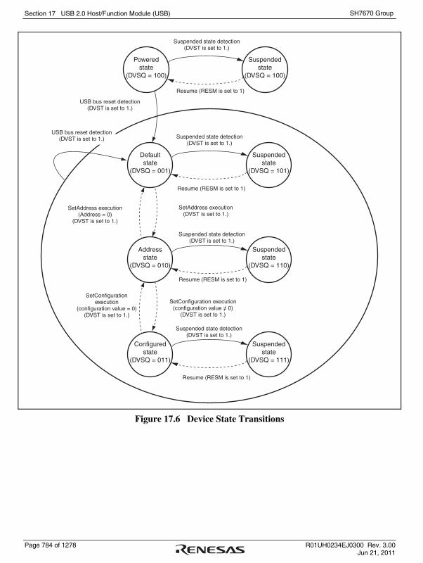
Section 17 USB 2.0 Host/Function Module (USB)
Page 784 of 1278 R01UH0234EJ0300 Rev. 3.00 Jun 21, 2011
SH7670 Group
Poweredstate
(DVSQ = 100)
Suspendedstate
(DVSQ = 100)
Defaultstate
(DVSQ = 001)
Suspendedstate
(DVSQ = 101)
Addressstate
(DVSQ = 010)
Suspendedstate
(DVSQ = 110)
Configuredstate
(DVSQ = 011)
Suspendedstate
(DVSQ = 111)
Suspended state detection(DVST is set to 1.)
USB bus reset detection(DVST is set to 1.)
Suspended state detection(DVST is set to 1.)
Suspended state detection(DVST is set to 1.)
SetAddress execution(DVST is set to 1.)
SetAddress execution(Address = 0)
(DVST is set to 1.)
Suspended state detection(DVST is set to 1.)
SetConfiguration execution(configuration value = 0)
(DVST is set to 1.)
SetConfigurationexecution
(configuration value = 0)(DVST is set to 1.)
Resume (RESM is set to 1)
Resume (RESM is set to 1)
Resume (RESM is set to 1)
Resume (RESM is set to 1)
USB bus reset detection(DVST is set to 1.)
/
Figure 17.6 Device State Transitions

Section 17 USB 2.0 Host/Function Module (USB)
R01UH0234EJ0300 Rev. 3.00 Page 785 of 1278 Jun 21, 2011
SH7670 Group
(5) Control Transfer Stage Transition Interrupt
Figure 17.7 shows a diagram of how this module handles the control transfer stage transition. This module controls the control transfer sequence and generates control transfer stage transition interrupts. Control transfer stage transition interrupts can be enabled or disabled individually using INTENB0. The transfer stage that made a transition can be confirmed using the CTSQ bit in INTSTS0.
The control transfer stage transition interrupts are generated only when the function controller function is selected.
The control transfer sequence errors are described below. If an error occurs, the PID bit in DCPCTR is set to B'1x (STALL).
(a) During control read transfers
⎯ At the IN token of the data stage, an OUT or PING token is received when there have been no data transfers at all.
⎯ An IN token is received at the status stage
⎯ A packet is received at the status stage for which the data packet is DATAPID = DATA0 (b) During control write transfers
⎯ At the OUT token of the data stage, an IN token is received when there have been no ACK response at all
⎯ A packet is received at the data stage for which the first data packet is DATAPID = DATA0
⎯ At the status stage, an OUT or PING token is received

Section 17 USB 2.0 Host/Function Module (USB)
Page 786 of 1278 R01UH0234EJ0300 Rev. 3.00 Jun 21, 2011
SH7670 Group
(c) During no-data control transfers
⎯ At the status stage, an OUT or PING token is received At the control write transfer stage, if the number of receive data exceeds the wLength value of the USB request, it cannot be recognized as a control transfer sequence error. At the control read transfer status stage, packets other than zero-length packets are received by an ACK response and the transfer ends normally.
When a CTRT interrupt occurs in response to a sequence error (SERR = 1), the CTSQ = 110 value is retained until CTRT = 0 is written from the system (the interrupt status is cleared). Therefore, while CTSQ = 110 is being held, the CTRT interrupt that ends the setup stage will not be generated even if a new USB request is received. (This module retains the setup stage end, and after the interrupt status has been cleared by software, a setup stage end interrupt is generated.)
1CTSQ = 001 control readdata stage
2CTSQ = 010 control read status stage
4CTSQ = 000
idle stage
3CTSQ = 100 control write status stage
1
CTSQ = 101 control write
no data status stage
5CTSQ = 110
control transfersequence error
CTSQ = 000setup stage
1CTSQ = 011 control writedata stage
Setup token reception
Setup token reception
Setup token reception
Error detection
OUT token
IN token
ACK trans-
mission
ACKreception
ACKreception
Note:
CTRT interrupts(1) Setup stage completed(2) Control read transfer status stage transition(3) Control write transfer status stage transition(4) Control transfer completed(5) Control transfer sequence error
4
Error detection and IN token reception are valid at all stages in the box.
ACK trans-
mission
ACK transmission
ACK transmission
Figure 17.7 Control Transfer Stage Transitions

Section 17 USB 2.0 Host/Function Module (USB)
R01UH0234EJ0300 Rev. 3.00 Page 787 of 1278 Jun 21, 2011
SH7670 Group
(6) Frame Update Interrupt
Figure 17.8 shows an example of the SOFR interrupt output timing of this module. With the host controller function selected, an interrupt is generated at the timing at which the frame number is updated. With the function controller function selected, the SOFR interrupt is generated when the frame number is updated.
When the function controller function is selected, this module updates the frame number and generates an SOFR interrupt if it detects a new SOF packet during full-speed operation. During high-speed operation, however, this module does not update the frame number, or generates no SOFR interrupt until the module enters the μSOF locked state. Also, the SOF interpolation function is not activated. The μSOF lock state is the state in which μSOF packets with different frame numbers are received twice continuously without error occurrence.
The conditions under which the μSOF lock monitoring begins and stops are as follows.
1. Conditions under which μSOF lock monitoring begins USBE = 1
2. Conditions under which μSOF lock monitoring stops USBE = 0, a USB bus reset is received, or suspended state is detected.
6
7 0 1 6 7 0 7 0 1 7 0 17 0 1 2
7 0 1 2 3 4 5 6 7 0 1 2 3 4 5 6 7 0 1
3 4 6
Peripheral Device
µSOF packet
µSOF packet
µSOF lock
µSOF number
µSOF number
µSOF lock
Frame number
SOFR interrupt
SOFR interrupt
SOF interpolation
SOF interpolation function
SOF interpolation SOF interpolation
SOF interpolation,missingNot locked Not locked
Figure 17.8 Example of SOFR Interrupt Output Timing
Section 17 USB 2.0 Host/Function Module (USB)
Page 788 of 1278 R01UH0234EJ0300 Rev. 3.00 Jun 21, 2011
SH7670 Group
(7) VBUS Interrupt
If there has been a change in the VBUS pin, the VBUS interrupt is generated. The level of the VBUS pin can be checked with the VBSTS bit in INTSTS0. Whether the host controller is connected or disconnected can be confirmed using the VBUS interrupt. However, if the system is activated with the host controller connected, the first VBUS interrupt is not generated because there is no change in the VBUS pin.
(8) Resume Interrupt
The RESM interrupt is generated when the device state is the suspended state, and the USB bus state has changed (from J-state to K-state, or from J-state to SE0). Recovery from the suspended state is detected by means of the resume interrupt.
(9) BCHG Interrupt
The BCHG interrupt is generated when the USB bus state has changed. The BCHG interrupt can be used to detect whether or not the peripheral device is connected when the host controller function has been selected and can also be used to detect a remote wakeup. The BCHG interrupt is generated regardless of whether the host controller function or function controller function has been selected.
(10) DTCH Interrupt
The DTCH interrupt is generated if disconnection of the USB bus is detected when the host controller function has been selected. This module detects bus disconnection based on USB Specification 2.0.
After detecting the DTCH interrupt, this module controls hardware as described below (irrespective of the set value of the corresponding interrupt enable bit). Software should terminate all the pipes in which communications are currently carried out for the pertinent port and make a transition to the wait state for bus connection to the pertinent port (wait state for ATTCH interrupt generation).
(a) Modifies the UACT bit for the port in which a DTCH interrupt has been detected to 0.
(b) Puts the port in which a DTCH interrupt has been generated into the idle state.
Section 17 USB 2.0 Host/Function Module (USB)
R01UH0234EJ0300 Rev. 3.00 Page 789 of 1278 Jun 21, 2011
SH7670 Group
(11) SACK Interrupt
The SACK interrupt is generated when an ACK response for the transmitted setup packet has been received from the peripheral device with the host controller function selected. The SACK interrupt can be used to confirm that the setup transaction has been completed successfully.
(12) SIGN Interrupt
The SIGN interrupt is generated when an ACK response for the transmitted setup packet has not been correctly received from the peripheral device three consecutive times with the host controller function selected. The SIGN interrupt can be used to detect no ACK response transmitted from the peripheral device or corruption of an ACK packet.
(13) ATTCH Interrupt
The ATTCH interrupt is generated when J-state or K-state of the full-speed or low-speed level signal is detected on the USB port for 2.5 μs in host controller mode. To be more specific, the ATTCH interrupt is detected on any of the following conditions.
(a) When K-state, SE0, or SE1 changes to J-state, and J-state continues 2.5 μs.
(b) When J-state, SE0, or SE1 changes to K-state, and K-state continues 2.5 μs.
(14) EOFERR Interrupt
The EOFERR interrupt is generated when it is detected that communication is not completed at the EOF2 timing prescribed by USB Specification 2.0.
After detecting the EOFERR interrupt, this module controls hardware as described below (irrespective of the set value of the corresponding interrupt enable bit). Software should terminate all the pipes in which communications are currently carried out for the pertinent port and perform re-enumeration of the pertinent port.
(a) Modifies the UACT bit for the port in which an EOFERR interrupt has been detected to 0.
(b) Puts the port in which an EOFERR interrupt has been generated into the idle state.

Section 17 USB 2.0 Host/Function Module (USB)
Page 790 of 1278 R01UH0234EJ0300 Rev. 3.00 Jun 21, 2011
SH7670 Group
17.4.3 Pipe Control
Table 17.18 lists the pipe setting items of this module. With USB data transfer, data transmission has to be carried out using the logic pipe called the endpoint. This module has ten pipes that are used for data transfer.
Settings should be entered for each of the pipes in conjunction with the specifications of the system.
Table 17.18 Pipe Setting Items
Register Name Bit Name
Setting Contents Remarks
TYPE Specifies the transfer type
PIPE1 to PIPE9: Can be set
BFRE Selects the BRDY interrupt mode
PIPE1 to PIPE5: Can be set
DBLB Selects a double buffer
PIPE1 to PIPE5: Can be set
CNTMD Selects continuous transfer or non-continuous transfer
PIPE1 and PIPE2: Can be set (only when bulk transfer has been selected).
PIPE3 to PIPE5: Can be set
DIR Selects transfer direction
IN or OUT can be set
EPNUM Endpoint number PIPE1 to PIPE9: Can be set
A value other than 0000 should be set when the pipe is used.
DCPCFG
PIPECFG
SHTNAK Selects disabled state for pipe when transfer ends
PIPE1 and PIPE2: Can be set (only when bulk transfer has been selected)
PIPE3 to PIPE5: Can be set
PIPEBUF BUFSIZE Buffer memory size
DCP: Cannot be set (fixed at 256 bytes)
PIPE1 to PIPE5: Can be set (a maximum of 2 Kbytes can be specified)
PIPE6 to PIPE9: Cannot be set (fixed at 64 bytes)

Section 17 USB 2.0 Host/Function Module (USB)
R01UH0234EJ0300 Rev. 3.00 Page 791 of 1278 Jun 21, 2011
SH7670 Group
Register Name Bit Name
Setting Contents Remarks
PIPEBUF BUFNMB Buffer memory number
DCP: Cannot be set (areas fixed at H'0 to H'3)
PIPE1 to PIPE5: Can be set (can be specified in areas H'8 to H'7F)
PIPE6 to PIPE9: Cannot be set (areas fixed at H'4 toH'7)
DEVSEL Selects a device Referenced only when the host controller function is selected.
DCPMAXP
PIPEMAXP MXPS Maximum packet
size Compliant with the USB standard.
IFIS Buffer flush PIPE1 and PIPE2: Can be set (only when isochronous transfer has been selected)
PIPE3 to PIPE5: Cannot be set
PIPE6 to PIPE9: Can be set (only when the host controller function has been selected)
PIPEPERI
IITV Interval counter PIPE1 and PIPE2: Can be set (only when isochronous transfer has been selected)
PIPE3 to PIPE5: Cannot be set
PIPE6 to PIPE9: Can be set (only when the host controller function has been selected)
BSTS Buffer status For the DCP, receive buffer status and transmit buffer status are switched with the ISEL bit.
INBUFM IN buffer monitor Mounted for PIPE3 to PIPE5.
SUREQ SETUP request Can be set only for the DCP.
Can be controlled only when the host controller function has been selected.
SUREQCLR SUREQ clear Can be set only for the DCP.
Can be controlled only when the host controller function has been selected.
CSCLR CSSTS clear Can be controlled only when the host controller function has been selected.
DCPCTR
PIPEnCTR
CSSTS SPLIT status indication
Can be referenced only when the host controller function has been selected.

Section 17 USB 2.0 Host/Function Module (USB)
Page 792 of 1278 R01UH0234EJ0300 Rev. 3.00 Jun 21, 2011
SH7670 Group
Register Name Bit Name
Setting Contents Remarks
ATREPM Auto response mode
PIPE1 to PIPE5: Can be set
Can be controlled only when the function controller function has been selected.
ACLRM Auto buffer clear PIPE1 to PIPE9: Can be set
SQCLR Sequence clear Clears the data toggle bit
SQSET Sequence set Sets the data toggle bit
SQMON Sequence monitor
Monitors the data toggle bit
PBUSY Pipe busy status
DCPCTR
PIPEnCTR
PID Response PID See section 17.4.3 (6), Response PID
TRENB Transaction counter enable
PIPE1 to PIPE5: Can be set PIPEnTRE
TRCLR Current transaction counter clear
PIPE1 to PIPE5: Can be set
PIPEnTRN TRNCNT Transaction counter
PIPE1 to PIPE5: Can be set
Section 17 USB 2.0 Host/Function Module (USB)
R01UH0234EJ0300 Rev. 3.00 Page 793 of 1278 Jun 21, 2011
SH7670 Group
(1) Pipe control register switching procedures
The following bits in the pipe control registers can be modified only when USB communication is disabled (PID = NAK):
Registers that Should Not be Set in the USB Communication Enabled (PID = BUF) State
• Bits in DCPCFG and DCPMAXP
• The SQCLR and SQSET bits in DCPCTR
• Bits in PIPECFG, PIPEBUF, PIPEMAXP and PIPEPERI
• The ATREPM, ACLRM, SQCLR and SQSET bits in PIPExCTR
• Bits in PIPExTRE and PIPExTRN In order to modify the above bits from the USB communication enabled (PID = BUF) state, follow the procedure shown below:
1. Generate a bit modification request with the pipe control register.
2. Modify the PID corresponding to the pipe to NAK.
3. Wait until the corresponding CSSTS bit is cleared to 0 (only when the host controller function has been selected).
4. Wait until the corresponding PBUSY bit is cleared to 0.
5. Modify the bits in the pipe control register. The following bits in the pipe control registers can be modified only when the pertinent information has not been set by the CURPIPE bits in CFIFOSEL, D0FIFOSEL and D1FIFOSEL.
Registers that Should Not be Set When CURPIPE in FIFO-PORT is set.
• Bits in DCPCFG and DCPMAXP
• Bits in PIPECFG, PIPEBUF, PIPEMAXP and PIPEPERI In order to modify pipe information, the CURPIPE bits should be set to the pipes other than the pipe to be modified. For the DCP, the buffer should be cleared using BCLR after the pipe information is modified.

Section 17 USB 2.0 Host/Function Module (USB)
Page 794 of 1278 R01UH0234EJ0300 Rev. 3.00 Jun 21, 2011
SH7670 Group
(2) Transfer Types
The TYPE bit in PIPEPCFG is used to specify the transfer type for each pipe. The transfer types that can be set for the pipes are as follows.
1. DCP: No setting is necessary (fixed at control transfer).
2. PIPE1 and PIPE2: These should be set to bulk transfer or isochronous transfer.
3. PIPE3 to PIPE5: These should be set to bulk transfer.
4. PIPE6 to PIPE9: These should be set to interrupt transfer. (3) Endpoint Number
The EPNUM bit in PIPEPCFG is used to set the endpoint number for each pipe. The DCP is fixed at endpoint 0. The other pipes can be set from endpoint 1 to endpoint 15.
1. DCP: No setting is necessary (fixed at end point 0).
2. PIPE1 to PIPE9: The endpoint numbers from 1 to 15 should be selected and set.
These should be set so that the combination of the DIR bit and EPNUM bit is unique. (4) Maximum Packet Size Setting
The MXPS bit in DCPMAXP and PIPEMAXP is used to specify the maximum packet size for each pipe. DCP and PIPE1 to PIPE5 can be set to any of the maximum pipe sizes defined by the USB specification. For PIPE6 to PIPE9, 64 bytes are the upper limit of the maximum packet size. The maximum packet size should be set before beginning the transfer (PID = BUF).
1. DCP: 64 should be set when using high-speed operation.
2. DCP: Select and set 8, 16, 32, or 64 when using full-speed operation.
3. PIPE1 to PIPE5: 512 should be set when using high-speed bulk transfer.
4. PIPE1 to PIPE5: Select and set 8, 16, 32, or 64 when using full-speed bulk transfer.
5. PIPE1 and PIPE2: Set a value between 1 and 1024 when using high-speed isochronous transfer.
6. PIPE1 and PIPE2: Set a value between 1 and 1023 when using full-speed isochronous transfer.
7. PIPE6 to PIPE9: Set a value between 1 and 64. The high bandwidth transfers used with interrupt transfers and isochronous transfers are not supported.

Section 17 USB 2.0 Host/Function Module (USB)
R01UH0234EJ0300 Rev. 3.00 Page 795 of 1278 Jun 21, 2011
SH7670 Group
(5) Transaction Counter (For PIPE1 to PIPE5 in Reading Direction)
When the specified number of transactions have been completed in the data packet receiving direction, this module recognizes that the transfer has ended. The transaction counter function is available when the pipes assigned to the D0FIFO/D1FIFO port have been set in the direction of reading data from the buffer memory. Two transaction counters are provided: one is the TRNCNT register that specifies the number of transactions to be executed and the other is the current counter that internally counts the number of executed transactions. When the current counter value matches the number of the transactions specified in TRNCNT, reading the buffer memory is enabled. The current counter of the transaction counter function is initialized by the TRCLR bit, so that the transactions can be counted again starting from the beginning. The information read from TRNCNT differs depending on the setting of the TRENB bit.
• TRENB = 0: The specified transaction counter value can be read.
• TRENB = 1: The current counter value indicating the internally counted number of executed transactions can be read.
When operating the TRCLR bit, the following should be noted.
• If the transactions are being counted and PID = BUF, the current counter cannot be cleared.
• If there is any data left in the buffer, the current counter cannot be cleared. (6) Response PID
The PID bits in DCPCTR and PIPEnCTR are used to set the response PID for each pipe.
The following shows this module operation with various response PID settings:
(a) Response PID settings when the host controller function is selected:
The response PID is used to specify the execution of transactions.
(i) NAK setting: Using pipes is disabled. No transaction is executed.
(ii) BUF setting: Transactions are executed based on the status of the buffer memory. For OUT direction: If there are transmit data in the buffer memory, an OUT token is issued. For IN direction: If there is an area to receive data in the buffer memory, an IN token is issued.
(iii) STALL setting: Using pipes is disabled. No transaction is executed.
Setup transactions for the DCP are set with the SUREQ bit.
Section 17 USB 2.0 Host/Function Module (USB)
Page 796 of 1278 R01UH0234EJ0300 Rev. 3.00 Jun 21, 2011
SH7670 Group
(b) Response PID settings when the function controller function is selected:
The response PID is used to specify the response to transactions from the host.
(i) NAK setting: The NAK response is always returned in response to the generated transaction.
(ii) BUF setting: Responses are made to transactions based on the status of the buffer memory.
(iii) STALL setting: The STALL response is always returned in response to the generated transaction.
For setup transactions, an ACK response is always returned, regardless of the PID setting, and the USB request is stored in the register.
This module may carry out writing to the PID bits, depending on the results of the transaction.
(c) When the host controller function has been selected and the response PID is set by hardware:
(i) NAK setting: In the following cases, PID = NAK is set and issuing of tokens is automatically stopped:
• When a transfer other than isochronous transfer has been performed and the NRDY interrupt is generated. (For details, see descriptions of the NRDY interrupt.)
• If a short packet is received when the SHTNAK bit in PIPECFG has been set to 1 for bulk transfer.
• If the transaction counter ended when the SHTNAK bit has been set to 1 for bulk transfer.
(ii) BUF setting: There is no BUF writing by this module.
(iii) STALL setting: In the following cases, PID = STALL is set and issuing of tokens is automatically stopped:
• When STALL is received in response to the transmitted token.
• When the size of the receive data packet exceeds the maximum packet size.

Section 17 USB 2.0 Host/Function Module (USB)
R01UH0234EJ0300 Rev. 3.00 Page 797 of 1278 Jun 21, 2011
SH7670 Group
(d) When the function controller function has been selected and the response PID is set by hardware:
(i) NAK setting: In the following cases, PID = NAK is set and NAK is always returned in response to transactions:
• When the SETUP token is received normally (DCP only).
• If the transaction counter ended or a short packet is received when the SHTNAK bit in PIPECFG has been set to 1 for bulk transfer.
(ii) BUF setting: There is no BUF writing by this module.
(iii) STALL setting: In the following cases, PID = STALL is set and STALL is always returned in response to transactions:
• When the size of the receive data packet exceeds the maximum packet size.
• When a control transfer sequence error has been detected (DCP only). (7) Data PID Sequence Bit
This module automatically toggles the sequence bit in the data PID when data is transferred normally in the control transfer data stage, bulk transfer and interrupt transfer. The sequence bit of the data PID that was transmitted can be confirmed with the SQMON bit in DCPCTR and PIPEnCTR. When data is transmitted, the sequence bit switches at the timing at which the ACK handshake is received. When data is received, the sequence bit switches at the timing at which the ACK handshake is transmitted. The SQCLR bit in DCPCTR and the SQSET bit in PIPEnCTR can be used to change the data PID sequence bit.
When the function controller function has been selected and control transfer is used, this module automatically sets the sequence bit when a stage transition is made. DATA0 is returned when the setup stage is ended and DATA1 is returned in a status stage. Therefore, software settings are not required. However, when the host controller function has been selected and control transfer is used, the sequence bit should be set by software at the stage transition.
For the Clearfeature request transmission or reception, the data PID sequence bit should be set by software, regardless of whether the host controller function or function controller function is selected.
With pipes for which isochronous transfer has been set, sequence bit operation cannot be carried out using the SQSET bit.

Section 17 USB 2.0 Host/Function Module (USB)
Page 798 of 1278 R01UH0234EJ0300 Rev. 3.00 Jun 21, 2011
SH7670 Group
(8) Response PID = NAK Function
This module has a function that disables pipe operation (PID response = NAK) at the timing at which the final data packet of a transaction is received (this module automatically distinguishes this based on reception of a short packet or the transaction counter) by setting the SHTNAK bit in PIPECFG to 1.
When a double buffer is being used for the buffer memory, using this function enables reception of data packets in transfer units. If pipe operation has disabled, the pipe has to be set to the enabled state again (PID response = BUF) using software.
This function can be used only when bulk transfers are used.
(9) Auto Transfer MODE
With the pipes for bulk transfer (PIPE1 to PIPE5), when the ATREPM bit in PIPEnCTR is set to 1, a transition is made to auto response mode. During an OUT transfer (DIR = 0), OUT-NAK mode is entered, and during an IN transfer (DIR = 1), null auto response mode is entered.
(a) OUT-NAK Mode
With the pipes for bulk OUT transfer, NAK is returned in response to an OUT or PING token and an NRDY interrupt is output when the ATREPM bit is set to 1. To make a transition from normal mode to OUT-NAK mode, OUT-NAK mode should be specified in the pipe operation disabled state (response PID = NAK) before enabling pipe operation (response PID = BUF). After pipe operation has been enabled, OUT-NAK mode becomes valid. However, if an OUT token is received immediately before pipe operation is disabled, the token data is normally received, and an ACK is retuned to the host.
To make a transition from OUT-NAK mode to normal mode, OUT-NAK mode should be canceled in the pipe operation disabled state (response PID = NAK) before enabling pipe operation (response PID = BUF). In normal mode, reception of OUT data is enabled and an ACK is returned in response to a PING token if the buffer is ready to receive data.

Section 17 USB 2.0 Host/Function Module (USB)
R01UH0234EJ0300 Rev. 3.00 Page 799 of 1278 Jun 21, 2011
SH7670 Group
(b) Null Auto Response Mode
With the pipes for bulk IN transfer, zero-length packets are continuously transmitted when the ATREPM bit is set to 1.
To make a transition from normal mode to null auto response mode, null auto response mode should be set in the pipe operation disabled state (response PID = NAK) before enabling pipe operation (response PID = BUF). After pipe operation has been enabled, null auto response mode becomes valid. Before setting null auto response mode, INBUFM = 0 should be confirmed because the mode can be set only when the buffer is empty. If the INBUFM bit is 1, the buffer should be emptied with the ACLRM bit. While a transition to null auto response mode is being made, data should not be written from the FIFO port.
To make a transition from null auto response mode to normal mode, pipe operation disabled state (response PID = NAK) should be retained for the period of zero-length packet transmission (full-speed: 10 μs, high-speed: 3 μs) before canceling null auto response mode. In normal mode, data can be written from the FIFO port; therefore, packet transmission to the host is enabled by enabling pipe operation (response PID = BUF).

Section 17 USB 2.0 Host/Function Module (USB)
Page 800 of 1278 R01UH0234EJ0300 Rev. 3.00 Jun 21, 2011
SH7670 Group
17.4.4 FIFO Buffer Memory
(1) FIFO Buffer Memory Allocation
Figure 17.9 shows an example of a FIFO buffer memory map for this module. The FIFO buffer memory is an area shared by the CPU and this module. In the FIFO buffer memory status, there are times when the access right to the buffer memory is allocated to the user system (CPU side), and times when it is allocated to this module (SIE side).
The buffer memory sets independent areas for each pipe. In the memory areas, 64 bytes comprise one block, and the memory areas are set using the first block number of the number of blocks (specified using the BUFNMB and BUFSIZE bits in PIPEBUF).
Independent buffer memory areas should be set for each pipe. Each memory area can be set using the first block number and the number of blocks (specified using the BUFNMB and BUFSIZE bits in PIPEBUF), where one block comprises 64 bytes.
When continuous transfer mode has been selected using the CNTMD bit in PIPEnCFG, the BUFSIZE bits should be set so that the buffer memory size should be an integral multiple of the maximum packet size. When double buffer mode has been selected using the DBLB bit in PIPEnCFG, two planes of the memory area specified using the BUFSIZE bits in PIPEBUF can be assigned to a single pipe.
Moreover, three FIFO ports are used for access to the buffer memory (reading and writing data). A pipe is assigned to the FIFO port by specifying the pipe number using the CURPIPE bit in C/DnFIFOSEL.
The buffer statuses of the various pipes can be confirmed using the BSTS bit in DCPCTR and the INBUFM bit in PIPEnCTR. Also, the access right of the FIFO port can be confirmed using the FRDY bit in CFIFOCTR or DnFIFOCTR.

Section 17 USB 2.0 Host/Function Module (USB)
R01UH0234EJ0300 Rev. 3.00 Page 801 of 1278 Jun 21, 2011
SH7670 Group
Buffer Memory PIPEBUF registers
BUFNMB = 0, BUFSIZE = 3
BUFNMB = 4, BUFSIZE = 0
BUFNMB = 5, BUFSIZE = 0
BUFNMB = 6, BUFSIZE = 3
BUFNMB = 10, BUFSIZE = 7
BUFNMB = 18, BUFSIZE = 3
BUFNMB = 22, BUFSIZE = 7
BUFNMB = 28, BUFSIZE = 2
PIPE0
PIPE6
PIPE7
PIPE5
PIPE1
PIPE2
PIPE3
PIPE4
CURPIPE = 1
CURPIPE = 3
CURPIPE = 6
FIFO Port
CFIFO Port
D0FIFO Port
D1FIFO Port
Figure 17.9 Example of a Buffer Memory Map
(a) Buffer Status
Tables 17.19 and 17.20 show the buffer status. The buffer memory status can be confirmed using the BSTS bit in DCPCTR and the INBUFM bit in PIPEnCTR. The access direction for the buffer memory can be specified using either the DIR bit in PIPEnCFG or the ISEL bit in CFIFOSEL (when DCP is selected).
The INBUFM bit is valid for PIPE0 to PIPE5 in the sending direction.
For an IN pipe uses double buffer, software can refer the BSTS bit to monitor the buffer memory status of CPU side and the INBUFM bit to monitor the buffer memory status of SIE side. In the case like the BEMP interrupt may not shows the buffer empty status because the CPU (DMAC) writes data slowly, software can use the INBUFM bit to confirm the end of sending.

Section 17 USB 2.0 Host/Function Module (USB)
Page 802 of 1278 R01UH0234EJ0300 Rev. 3.00 Jun 21, 2011
SH7670 Group
Table 17.19 Buffer Status Indicated by the BSTS Bit
ISEL or DIR BSTS Buffer Memory State
0 (receiving direction) 0 There is no received data, or data is being received.
Reading from the FIFO port is inhibited.
0 (receiving direction) 1 There is received data, or a zero-length packet has been received.
Reading from the FIFO port is allowed.
However, because reading is not possible when a zero-length packet is received, the buffer must be cleared.
1 (transmitting direction)
0 The transmission has not been finished.
Writing to the FIFO port is inhibited.
1 (transmitting direction)
1 The transmission has been finished.
CPU write is allowed.
Table 17.20 Buffer Status Indicated by the INBUFM Bit
IDIR INBUFM Buffer Memory State
0 (receiving direction) Invalid Invalid
1 (transmitting direction)
0 The transmission has been finished.
There is no waiting data to be transmitted.
1 (transmitting direction)
1 The FIFO port has written data to the buffer.
There is data to be transmitted
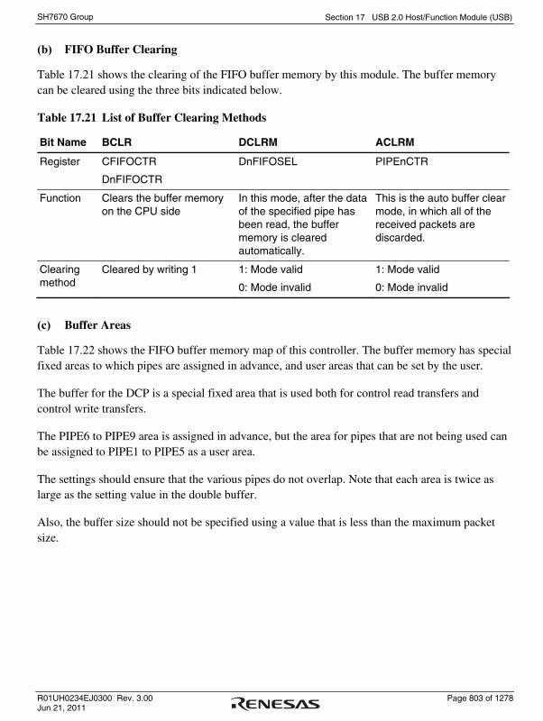
Section 17 USB 2.0 Host/Function Module (USB)
R01UH0234EJ0300 Rev. 3.00 Page 803 of 1278 Jun 21, 2011
SH7670 Group
(b) FIFO Buffer Clearing
Table 17.21 shows the clearing of the FIFO buffer memory by this module. The buffer memory can be cleared using the three bits indicated below.
Table 17.21 List of Buffer Clearing Methods
Bit Name BCLR DCLRM ACLRM
Register CFIFOCTR
DnFIFOCTR
DnFIFOSEL PIPEnCTR
Function Clears the buffer memory on the CPU side
In this mode, after the data of the specified pipe has been read, the buffer memory is cleared automatically.
This is the auto buffer clear mode, in which all of the received packets are discarded.
Clearing method
Cleared by writing 1 1: Mode valid
0: Mode invalid
1: Mode valid
0: Mode invalid
(c) Buffer Areas
Table 17.22 shows the FIFO buffer memory map of this controller. The buffer memory has special fixed areas to which pipes are assigned in advance, and user areas that can be set by the user.
The buffer for the DCP is a special fixed area that is used both for control read transfers and control write transfers.
The PIPE6 to PIPE9 area is assigned in advance, but the area for pipes that are not being used can be assigned to PIPE1 to PIPE5 as a user area.
The settings should ensure that the various pipes do not overlap. Note that each area is twice as large as the setting value in the double buffer.
Also, the buffer size should not be specified using a value that is less than the maximum packet size.

Section 17 USB 2.0 Host/Function Module (USB)
Page 804 of 1278 R01UH0234EJ0300 Rev. 3.00 Jun 21, 2011
SH7670 Group
Table 17.22 Buffer Memory Map
Buffer Memory Number Buffer Size Pipe Setting Note
H'0 64 bytes Fixed area only for the DCP
Single buffer, continuous transfers enabled
H'1 to H'3 ⎯ Prohibited to be used
⎯
H'4 64 bytes Fixed area for PIPE6
Single buffer
H'5 64 bytes Fixed area for PIPE7
Single buffer
H'6 64 bytes Fixed area for PIPE8
Single buffer
H'7 64 bytes Fixed area for PIPE9
Single buffer
H'8 to H'7F Up to 7616 bytes
PIPE1 to PIPE5 user area
Double buffer can be set, continuous transfers enabled
(d) Auto Buffer Clear Mode Function
With this module, all of the received data packets are discarded if the ACLRM bit in PIPEnCTR is set to 1. If a normal data packet has been received, the ACK response is returned to the host controller. This function can be set only in the buffer memory reading direction.
Also, if the ACLRM bit is set to 1 and then to 0, the buffer memory of the selected pipe can be cleared regardless of the access direction.
An access cycle of at least 100 ns is required between ACLRM = 1 and ACLRM = 0.
(e) Buffer Memory Specifications (Single/Double Setting)
Either a single or double buffer can be selected for PIPE1 to PIPE5, using the DBLB bit in PIPEnCFG. The double buffer is a function that assigns two memory areas specified with the BUFSIZE bit in PIPEBUF to the same pipe. Figure 17.10 shows an example of buffer memory settings for this module.
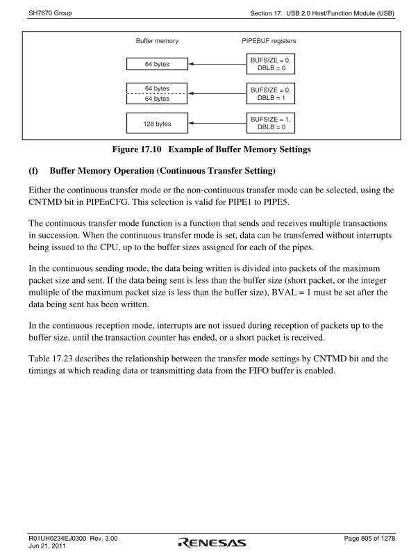
Section 17 USB 2.0 Host/Function Module (USB)
R01UH0234EJ0300 Rev. 3.00 Page 805 of 1278 Jun 21, 2011
SH7670 Group
Buffer memory PIPEBUF registers
64 bytes
64 bytes
64 bytes
128 bytes
BUFSIZE = 0, DBLB = 0
BUFSIZE = 0, DBLB = 1
BUFSIZE = 1, DBLB = 0
Figure 17.10 Example of Buffer Memory Settings
(f) Buffer Memory Operation (Continuous Transfer Setting)
Either the continuous transfer mode or the non-continuous transfer mode can be selected, using the CNTMD bit in PIPEnCFG. This selection is valid for PIPE1 to PIPE5.
The continuous transfer mode function is a function that sends and receives multiple transactions in succession. When the continuous transfer mode is set, data can be transferred without interrupts being issued to the CPU, up to the buffer sizes assigned for each of the pipes.
In the continuous sending mode, the data being written is divided into packets of the maximum packet size and sent. If the data being sent is less than the buffer size (short packet, or the integer multiple of the maximum packet size is less than the buffer size), BVAL = 1 must be set after the data being sent has been written.
In the continuous reception mode, interrupts are not issued during reception of packets up to the buffer size, until the transaction counter has ended, or a short packet is received.
Table 17.23 describes the relationship between the transfer mode settings by CNTMD bit and the timings at which reading data or transmitting data from the FIFO buffer is enabled.
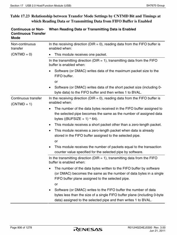
Section 17 USB 2.0 Host/Function Module (USB)
Page 806 of 1278 R01UH0234EJ0300 Rev. 3.00 Jun 21, 2011
SH7670 Group
Table 17.23 Relationship between Transfer Mode Settings by CNTMD Bit and Timings at which Reading Data or Transmitting Data from FIFO Buffer is Enabled
Continuous or Non- Continuous Transfer Mode
When Reading Data or Transmitting Data is Enabled
In the receiving direction (DIR = 0), reading data from the FIFO buffer is enabled when:
• This module receives one packet.
Non-continuous transfer
(CNTMD = 0)
In the transmitting direction (DIR = 1), transmitting data from the FIFO buffer is enabled when:
• Software (or DMAC) writes data of the maximum packet size to the
FIFO buffer.
or
• Software (or DMAC) writes data of the short packet size (including 0-
byte data) to the FIFO buffer and then writes 1 to BVAL.
In the receiving direction (DIR = 0), reading data from the FIFO buffer is enabled when:
• The number of the data bytes received in the FIFO buffer assigned to
the selected pipe becomes the same as the number of assigned data
bytes ((BUFSIZE + 1) * 64).
• This module receives a short packet other than a zero-length packet.
• This module receives a zero-length packet when data is already
stored in the FIFO buffer assigned to the selected pipe.
or
• This module receives the number of packets equal to the transaction
counter value specified for the selected pipe by software.
Continuous transfer
(CNTMD = 1)
In the transmitting direction (DIR = 1), transmitting data from the FIFO buffer is enabled when:
• The number of the data bytes written to the FIFO buffer by software
(or DMAC) becomes the same as the number of data bytes in a single
FIFO buffer plane assigned to the selected pipe.
or
• Software (or DMAC) writes to the FIFO buffer the number of data bytes less than the size of a single FIFO buffer plane (including 0-byte
data) assigned to the selected pipe and then writes 1 to BVAL.

Section 17 USB 2.0 Host/Function Module (USB)
R01UH0234EJ0300 Rev. 3.00 Page 807 of 1278 Jun 21, 2011
SH7670 Group
Figure 17.11 shows an example of buffer memory operation for this module.
CNTMD = 0When packet is received
CNTMD = 1When packet is received
CNTMD = 0When packet is sent
CNTMD = 1When packet is sent
Max Packet Size
Max Packet Size
Max Packet Size
Max Packet Size
Max Packet Size
Max Packet Size
Unused area
Unused area
Interrupt issued
Interrupt issued
Transmission enabled
Transmission enabled
Figure 17.11 Example of Buffer Memory Operation
(2) FIFO Port Functions
Table 17.24 shows the settings for the FIFO port functions of this module. In write access, writing data until the buffer is full (or the maximum packet size for non-continuous transfers) automatically enables sending of the data. To enable sending of data before the buffer is full (or before the maximum packet size for non-continuous transfers), the BVAL bit in C/DnFIFOCTR must be set to end the writing. Also, to send a zero-length packet, the BCLR bit in the same register must be used to clear the buffer and then the BVAL bit set in order to end the writing.
In read access, reception of new packets is automatically enabled if all of the data has been read. Data cannot be read when a zero-length packet is being received (DTLN = 0), so the BCLR bit in the register must be used to release the buffer. The length of the data being received can be confirmed using the DTLN bit in C/DnFIFOCTR.

Section 17 USB 2.0 Host/Function Module (USB)
Page 808 of 1278 R01UH0234EJ0300 Rev. 3.00 Jun 21, 2011
SH7670 Group
Table 17.24 FIFO Port Function Settings
Register Name Bit Name Function Note
RCNT Selects DTLN read mode
REW Buffer memory rewind (re-read, rewrite)
DCLRM Automatically clears data received for a specified pipe after the data has been read
For DnFIFO only
DREQE Enables DMA transfers For DnFIFO only
MBW FIFO port access bit width
BIGEND Selects FIFO port endian
ISEL FIFO port access direction
C/DnFIFOSEL
CURPIPE Selects the current pipe For DCP only
BVAL Ends writing to the buffer memory
BCLR Clears the buffer memory on the CPU side
C/DnFIFOCTR
DTLN Checks the length of received data
(a) FIFO Port Selection
Table 17.25 shows the pipes that can be selected with the various FIFO ports. The pipe to be accessed is selected using the CURPIPE bit in C/DnFIFOSEL. After the pipe is selected, whether the CURPIPE value for the pipe which was written last can be correctly read should be checked. (If the previous pipe number is read, it indicates that the pipe modification is being executed by this module.) Then, the FIFO port can be accessed after FRDY = 1 is checked .
Also, the bus width to be accessed should be selected using the MBW bit. The buffer memory access direction conforms to the DIR bit in PIPEnCFG. The ISEL bit determines this only for the DCP.
Table 17.25 FIFO Port Access Categorized by Pipe
Pipe Access Method Port that can be Used
DCP CPU access CFIFO port register
CPU access CFIFO port register
D0FIFO/D1FIFO port register
PIPE1 to PIPE9
DMA access D0FIFO/D1FIFO port register

Section 17 USB 2.0 Host/Function Module (USB)
R01UH0234EJ0300 Rev. 3.00 Page 809 of 1278 Jun 21, 2011
SH7670 Group
(b) REW Bit
It is possible to temporarily stop access to the pipe currently being accessed, access a different pipe, and then continue processing using the current pipe once again. The REW bit in C/DnFIFOSEL is used for this.
If a pipe is selected when the REW bit is set to 1 and at the same time the CURPIPE bit in C/DnFIFOSEL is set, the pointer used for reading from and writing to the buffer memory is reset, and reading or writing can be carried out from the first byte. Also, if a pipe is selected with 0 set for the REW bit, data can be read and written in continuation of the previous selection, without the pointer used for reading from and writing to the buffer memory being reset.
To access the FIFO port, FRDY = 1 must be ensured after selecting a pipe.
(3) DMA Transfers (D0FIFO/D1FIFO port)
(a) Overview of DMA Transfers
For pipes 1 to 9, the FIFO port can be accessed using the DMAC. When accessing the buffer for the pipe targeted for DMA transfer is enabled, a DMA transfer request is issued.
The unit of transfer to the FIFO port should be selected using the MBW bit in DnFIFOSEL and the pipe targeted for the DMA transfer should be selected using the CURPIPE bit. The selected pipe should not be changed during the DMA transfer.
(b) Auto Recognition of DMA Transfer Completion
With this module, it is possible to complete FIFO data writing through DMA transfer by controlling DMA transfer end signal input. When a transfer end signal is sampled, the module enables buffer memory transmission (the same condition as when BVAL = 1).
(c) DnFIFO Auto Clear Mode (D0FIFO/D1FIFO Port Reading Direction)
If 1 is set for the DCLRM bit in DnFIFOSEL, the module automatically clears the buffer memory of the selected pipe when reading of the data from the buffer memory has been completed.
Table 17.26 shows the packet reception and buffer memory clearing processing for each of the various settings. As shown, the buffer clear conditions depend on the value set to the BFRE bit. Using the DCLRM bit eliminates the need for the buffer to be cleared by software even if a situation occurs that necessitates clearing of the buffer. This makes it possible to carry out DMA transfers without involving software.
This function can be set only in the buffer memory reading direction.
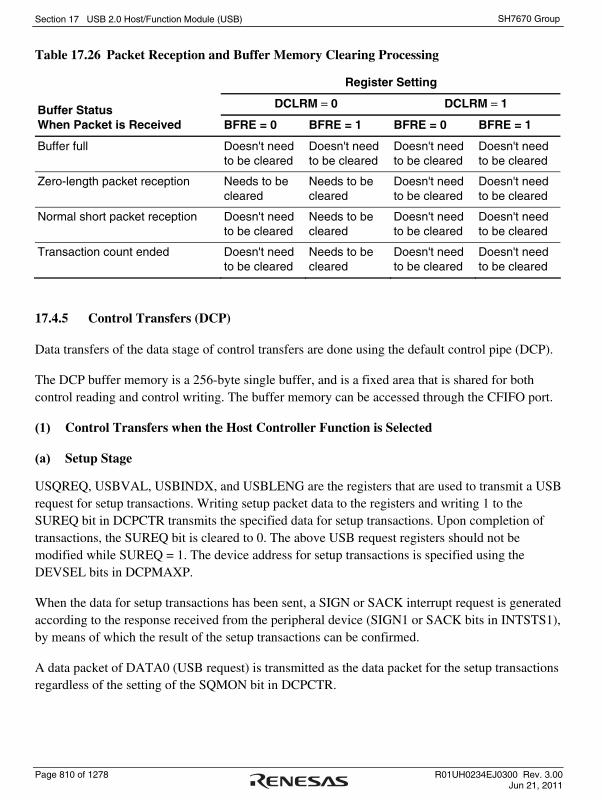
Section 17 USB 2.0 Host/Function Module (USB)
Page 810 of 1278 R01UH0234EJ0300 Rev. 3.00 Jun 21, 2011
SH7670 Group
Table 17.26 Packet Reception and Buffer Memory Clearing Processing
Register Setting
DCLRM = 0 DCLRM = 1 Buffer Status When Packet is Received BFRE = 0 BFRE = 1 BFRE = 0 BFRE = 1
Buffer full Doesn't need to be cleared
Doesn't need to be cleared
Doesn't need to be cleared
Doesn't need to be cleared
Zero-length packet reception Needs to be cleared
Needs to be cleared
Doesn't need to be cleared
Doesn't need to be cleared
Normal short packet reception Doesn't need to be cleared
Needs to be cleared
Doesn't need to be cleared
Doesn't need to be cleared
Transaction count ended Doesn't need to be cleared
Needs to be cleared
Doesn't need to be cleared
Doesn't need to be cleared
17.4.5 Control Transfers (DCP)
Data transfers of the data stage of control transfers are done using the default control pipe (DCP).
The DCP buffer memory is a 256-byte single buffer, and is a fixed area that is shared for both control reading and control writing. The buffer memory can be accessed through the CFIFO port.
(1) Control Transfers when the Host Controller Function is Selected
(a) Setup Stage
USQREQ, USBVAL, USBINDX, and USBLENG are the registers that are used to transmit a USB request for setup transactions. Writing setup packet data to the registers and writing 1 to the SUREQ bit in DCPCTR transmits the specified data for setup transactions. Upon completion of transactions, the SUREQ bit is cleared to 0. The above USB request registers should not be modified while SUREQ = 1. The device address for setup transactions is specified using the DEVSEL bits in DCPMAXP.
When the data for setup transactions has been sent, a SIGN or SACK interrupt request is generated according to the response received from the peripheral device (SIGN1 or SACK bits in INTSTS1), by means of which the result of the setup transactions can be confirmed.
A data packet of DATA0 (USB request) is transmitted as the data packet for the setup transactions regardless of the setting of the SQMON bit in DCPCTR.

Section 17 USB 2.0 Host/Function Module (USB)
R01UH0234EJ0300 Rev. 3.00 Page 811 of 1278 Jun 21, 2011
SH7670 Group
(b) Data Stage
Data transfers are done using the DCP buffer memory.
The access direction of the DCP buffer memory should be specified using the ISEL bit in CFIFOSEL.
For the first data packet of the data stage, the data PID must be transferred as DATA1. Transaction is done by setting the data PID = DATA1 and the PID bit = BUF using the SQSET bit in DCPCFG. Completion of data transfer is detected using the BRDY and BEMP interrupts.
Setting continuous transfer mode allows data transfers over multiple packets. Note that when continuous transfer mode is set for the receiving direction, the BRDY interrupt is not generated until the buffer becomes full or a short packet is received (the integer multiple of the maximum packet size, and less than 256 bytes).
For control write transfers, when the number of data bytes to be sent is the integer multiple of the maximum packet size, software must control so as to send a zero-length packet at the end.
(c) Status Stage
Zero-length packet data transfers are done in the direction opposite to that in the data stage. As with the data stage, data transfers are done using the DCP buffer memory. Transactions are done in the same manner as the data stage.
For the data packets of the status stage, the data PID must be transferred as DATA1. The data PID should be set to DATA1 using the SQSET bit in DCPCFG.
For reception of a zero-length packet, the received data length must be confirmed using the DTLN bits in CFIFOCTR after the BRDY interrupt is generated, and the buffer memory must then be cleared using the BCLR bit.
Section 17 USB 2.0 Host/Function Module (USB)
Page 812 of 1278 R01UH0234EJ0300 Rev. 3.00 Jun 21, 2011
SH7670 Group
(2) Control Transfers when the Function Controller Function is Selected
(a) Setup Stage
This module always sends an ACK response in response to a setup packet that is normal with respect to this module. The operation of this module operates in the setup stage is noted below.
(i) When a new USB request is received, this module sets the following registers:
• Set the VALID bit in INTSTS0 to 1.
• Set the PID bit in DCPCTR to NAK.
• Set the CCPL bit in DCPCTR to 0. (ii) When a data packet is received right after the SETUP packet, the USB request parameters are
stored in USBREQ, USBVAL, USBINDX, and USBLENG.
Response processing with respect to the control transfer should always be carried out after first setting VALID = 0. In the VALID = 1 state, PID = BUF cannot be set, and the data stage cannot be terminated.
Using the function of the VALID bit, this module is able to interrupt the processing of a request currently being processed if a new USB request is received during a control transfer, and can send a response in response to the newest request.
Also, this module automatically judges the direction bit (bit 8 of the bmRequestType) and the request data length (wLength) of the USB request that was received, and then distinguishes between control read transfers, control write transfers, and no-data control transfers, and controls the stage transition. For a wrong sequence, the sequence error of the control transfer stage transition interrupt is generated, and the software is notified. For information on the stage control of this module, see figure 17.7.
(b) Data Stage
Data transfers corresponding to USB requests that have been received should be done using the DCP. Before accessing the DCP buffer memory, the access direction should be specified using the ISEL bit in CFIFOSEL.
If the data being transferred is larger than the size of the DCP buffer memory, the data transfer should be carried out using the BRDY interrupt for control write transfers and the BEMP interrupt for control read transfers.
With control write transfers during high-speed operation, the NYET handshake response is carried out based on the state of the buffer memory.

Section 17 USB 2.0 Host/Function Module (USB)
R01UH0234EJ0300 Rev. 3.00 Page 813 of 1278 Jun 21, 2011
SH7670 Group
(c) Status Stage
Control transfers are terminated by setting the CCPL bit to 1 with the PID bit in DCPCTR set to PID = BUF.
After the above settings have been entered, this module automatically executes the status stage in accordance with the data transfer direction determined at the setup stage. The specific procedure is as follows.
(i) For control read transfers:
This module sends a zero-length packet and receives an ACK response from the USB host.
(ii) For control write transfers and no-data control transfers:
The zero-length packet is received from the USB host, and this module sends an ACK response.
(d) Control Transfer Auto Response Function
This module automatically responds to a normal SET_ADDRESS request. If any of the following errors occur in the SET_ADDRESS request, a response from the software is necessary.
(i) Any transfer other than a control read transfer: bmRequestType ≠ H'00
(ii) If a request error occurs: wIndex ≠ H'00
(ii) For any transfer other than a no-data control transfer: wLength ≠ H'00
(iv) If a request error occurs: wValue > H'7F
(v) Control transfer of a device state error: DVSQ = 011 (Configured)
For all requests other than the SET_ADDRESS request, a response is required from the corresponding software.
Section 17 USB 2.0 Host/Function Module (USB)
Page 814 of 1278 R01UH0234EJ0300 Rev. 3.00 Jun 21, 2011
SH7670 Group
17.4.6 Bulk Transfers (PIPE1 to PIPE5)
The buffer memory specifications for bulk transfers (single/double buffer setting, or continuous/non-continuous transfer mode setting) can be selected. The maximum size that can be set for the buffer memory is 2 Kbytes. The buffer memory state is controlled by this module, with a response sent automatically for a PING packet/NYET handshake.
(1) PING Packet Control when the Host Controller Function is Selected
This module automatically sends a PING packet in the OUT direction.
On receiving an ACK handshake in the initial state in which PING packet sending mode is set, this module sends an OUT packet as noted below. Reception of an NAK or NYET handshake returns this module to PING packet sending mode. This control also applies to the control transfers in the data stage and status stage.
1. Sets OUT data sending mode.
2. Sends a PING packet.
3. Receives an ACK handshake.
4. Sends an OUT data packet.
5. Receives an ACK handshake.
(Repeats steps 4 and 5.)
6. Sends an OUT data packet.
7. Receives an NAK/NYET handshake.
8. Sends a PING packet. This module is returned to PING packet sending mode by a power-on reset, receiving a NYET/NAK handshake, setting or clearing the sequence toggle bits (SQSET and SQCLR), and setting the buffer clear bit (ACLRM) in PIPEnCTR.
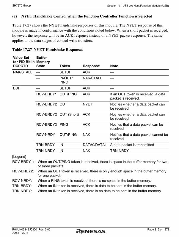
Section 17 USB 2.0 Host/Function Module (USB)
R01UH0234EJ0300 Rev. 3.00 Page 815 of 1278 Jun 21, 2011
SH7670 Group
(2) NYET Handshake Control when the Function Controller Function is Selected
Table 17.27 shows the NYET handshake responses of this module. The NYET response of this module is made in conformance with the conditions noted below. When a short packet is received, however, the response will be an ACK response instead of a NYET packet response. The same applies to the data stages of control write transfers.
Table 17.27 NYET Handshake Responses
Value Set for PID Bit in DCPCTR
Buffer Memory State Token Response Note
NAK/STALL ⎯ SETUP ACK ⎯
⎯ IN/OUT/ PING
NAK/STALL ⎯
BUF ⎯ SETUP ACK ⎯
RCV-BRDY1 OUT/PING ACK If an OUT token is received, a data packet is received.
RCV-BRDY2 OUT NYET Notifies whether a data packet can be received
RCV-BRDY2 OUT (Short) ACK Notifies whether a data packet can be received
RCV-BRDY2 PING ACK Notifies that a data packet can be received
RCV-NRDY OUT/PING NAK Notifies that a data packet cannot be received
TRN-BRDY IN DATA0/DATA1 A data packet is transmitted
TRN-NRDY IN NAK TRN-NRDY
[Legend] RCV-BRDY1: When an OUT/PING token is received, there is space in the buffer memory for two
or more packets. RCV-BRDY2: When an OUT token is received, there is only enough space in the buffer memory
for one packet. RCV-NRDY: When a PING token is received, there is no space in the buffer memory.
TRN-BRDY: When an IN token is received, there is data to be sent in the buffer memory.
TRN-NRDY: When an IN token is received, there is no data to be sent in the buffer memory.

Section 17 USB 2.0 Host/Function Module (USB)
Page 816 of 1278 R01UH0234EJ0300 Rev. 3.00 Jun 21, 2011
SH7670 Group
17.4.7 Interrupt Transfers (PIPE6 to PIPE9)
When the function controller function is selected, this module carries out interrupt transfers in accordance with the timing controlled by the host controller. For interrupt transfers, PING packets are ignored (no responses are sent), and the ACK, NAK, and STALL responses are carried out without an NYET handshake response being made.
When the host controller function is selected, this module can set the timing of issuing a token using the interval timer. At this time, this module issues an OUT token even in the OUT direction, without issuing a PING token.
This module does not support high bandwidth transfers of interrupt transfers.
(1) Interval Counter during Interrupt Transfers when the Host Controller Function is Selected
For interrupt transfers, intervals between transactions are set in the IITV bits in PIPEPERI. This controller issues an interrupt transfer token based on the specified intervals.
(a) Counter Initialization
This controller initializes the interval counter under the following conditions.
(i) Power-on reset:
The IITV bits are initialized.
(ii) Buffer memory initialization using the ACLRM bit:
The IITV bits are not initialized but the count value is. Setting the ACLRM bit to 0 starts counting from the value set in the IITV bits.
Note that the interval counter is not initialized in the following case.
(iii) USB bus reset, USB suspended:
The IITV bits are not initialized. Setting 1 to the UACT bit starts counting from the value before entering the USB bus reset state or USB suspended state.

Section 17 USB 2.0 Host/Function Module (USB)
R01UH0234EJ0300 Rev. 3.00 Page 817 of 1278 Jun 21, 2011
SH7670 Group
(b) Operation when Transmission/Reception is Impossible at Token Issuance Timing
This module cannot issue tokens even at token issuance timing in the following cases. In such a case, this module attempts transactions at the subsequent interval.
(i) When the PID is set to NAK or STALL.
(ii) When the buffer memory is full at the token sending timing in the receiving (IN) direction.
(iii) When there is no data to be sent in the buffer memory at the token sending timing in the sending (OUT) direction.
17.4.8 Isochronous Transfers (PIPE1 and PIPE2)
1. This module has the following functions pertaining to isochronous transfers.
2. Notification of isochronous transfer error information
3. Interval counter (specified by the IITV bit)
4. Isochronous IN transfer data setup control (IDLY function)
5. Isochronous IN transfer buffer flush function (specified by the IFIS bit) This module does not support the High Bandwidth transfers of isochronous transfers.
(1) Error Detection with Isochronous Transfers
This module has a function for detecting the error information noted below, so that when errors occur in isochronous transfers, software can control them. Tables 17.28 and 17.29 show the priority in which errors are confirmed and the interrupts that are generated.
(i) PID errors
• If the PID of the packet being received is illegal
(ii) CRC errors and bit stuffing errors
• If an error occurs in the CRC of the packet being received, or the bit stuffing is illegal
(iii) Maximum packet size exceeded
• The maximum packet size exceeded the set value.

Section 17 USB 2.0 Host/Function Module (USB)
Page 818 of 1278 R01UH0234EJ0300 Rev. 3.00 Jun 21, 2011
SH7670 Group
(iv) Overrun and underrun errors
• When host controller function is selected: ⎯ When using isochronous IN transfers (reception), the IN token was received but the buffer
memory is not empty.
⎯ When using isochronous OUT transfers (transmission), the OUT token was transmitted, but the data was not in the buffer memory.
• When function controller function is selected:
⎯ When using isochronous IN transfers (transmission), the IN token was received but the data was not in the buffer memory.
⎯ When using isochronous OUT transfers (reception), the OUT token was received, but the buffer memory was not empty.
(v) Interval errors
• During an isochronous IN transfer, the token could not be received during the interval frame.
• During an isochronous OUT transfer, the OUT token was received during frames other than the interval frame.
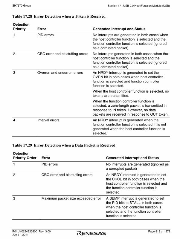
Section 17 USB 2.0 Host/Function Module (USB)
R01UH0234EJ0300 Rev. 3.00 Page 819 of 1278 Jun 21, 2011
SH7670 Group
Table 17.28 Error Detection when a Token is Received
Detection Priority Error Generated Interrupt and Status
1 PID errors No interrupts are generated in both cases when the host controller function is selected and the function controller function is selected (ignored as a corrupted packet).
2 CRC error and bit stuffing errors No interrupts generated in both cases when the host controller function is selected and the function controller function is selected (ignored as a corrupted packet).
3 Overrun and underrun errors An NRDY interrupt is generated to set the OVRN bit in both cases when host controller function is selected and function controller function is selected.
When the host controller function is selected, no tokens are transmitted.
When the function controller function is selected, a zero-length packet is transmitted in response to IN token. However, no data packets are received in response to OUT token.
4 Interval errors An NRDY interrupt is generated when the function controller function is selected. It is not generated when the host controller function is selected.
Table 17.29 Error Detection when a Data Packet is Received
Detection Priority Order Error Generated Interrupt and Status
1 PID errors No interrupts are generated (ignored as a corrupted packet)
2 CRC error and bit stuffing errors An NRDY interrupt is generated to set the CRCE bit in both cases when the host controller function is selected and the function controller function is selected.
3 Maximum packet size exceeded error A BEMP interrupt is generated to set the PID bits to STALL in both cases when the host controller function is selected and the function controller function is selected.

Section 17 USB 2.0 Host/Function Module (USB)
Page 820 of 1278 R01UH0234EJ0300 Rev. 3.00 Jun 21, 2011
SH7670 Group
(2) DATA-PID
This module does not support High Bandwidth transfers. When the function controller function is selected, this module operates as follows in response to the received PID.
(a) IN direction
⎯ DATA0: Sent as data packet PID ⎯ DATA1: Not sent ⎯ DATA2: Not sent ⎯ mDATA: Not sent
(b) OUT direction (when using full-speed operation)
⎯ DATA0: Received normally as data packet PID ⎯ DATA1: Received normally as data packet PID ⎯ DATA2: Packets are ignored ⎯ mDATA: Packets are ignored
(c) OUT direction (when using high-speed operation)
⎯ DATA0: Received normally as data packet PID ⎯ DATA1: Received normally as data packet PID ⎯ DATA2: Received normally as data packet PID ⎯ mDATA: Received normally as data packet PID

Section 17 USB 2.0 Host/Function Module (USB)
R01UH0234EJ0300 Rev. 3.00 Page 821 of 1278 Jun 21, 2011
SH7670 Group
(3) Interval Counter
The isochronous interval can be set using the IITV bits in PIPEPERI. The interval counter enables the functions shown in table 17.30 when the function controller function is selected. When the host controller function is selected, this module generates the token issuance timing. When the host controller function is selected, the interval counter operation is the same as the interrupt transfer operation.
Table 17.30 Functions of the Interval Counter when the Function Controller Function is Selected
Transfer Direction Function Conditions for Detection
IN IN buffer flush function When an IN token cannot be normally received in the interval frame during an isochronous IN transfer
OUT Notifies that a token not being received
When an OUT token cannot be normally received in the interval frame during an isochronous OUT transfer
The interval count is carried out when an SOF is received or for interpolated SOFs, so the isochronism can be maintained even if an SOF is damaged. The frame interval that can be set is the 2IITV frame or 2IITV μ frames.
(a) Counter Initialization when the Function Controller Function is Selected
This module initializes the interval counter under the following conditions.
(i) Power-on reset
The IITV bit is initialized.
(ii) Buffer memory initialization using the ACLRM bit
The IITV bits are not initialized but the count value is. Setting the ACLRM bit to 0 starts counting from the value set in the IITV bits.
After the interval counter has been initialized, the counter is started under the following conditions 1 or 2 when a packet has been transferred normally.
1. An SOF is received following transmission of data in response to an IN token, in the PID = BUF state.
2. An SOF is received after data following an OUT token is received in the PID = BUF state.

Section 17 USB 2.0 Host/Function Module (USB)
Page 822 of 1278 R01UH0234EJ0300 Rev. 3.00 Jun 21, 2011
SH7670 Group
The interval counter is not initialized under the conditions noted below.
1. When the PID bit is set to NAK or STALL
The interval timer does not stop. This module attempts the transactions at the subsequent interval.
2. The USB bus reset or the USB is suspended
The IITV bit is not initialized. When the SOF has been received, the counter is restarted from the value prior to the reception of the SOF.
(b) Interval Counting and Transfer Control when the Host Controller Function is Selected
This module controls the interval between token issuance operations based on the IITV bit settings. Specifically, this module issues a token for a selected pipe once every 2IITV (μ) frames.
This module counts the interval every 1-ms frame for the pipes used for communications with the full-speed or low-speed peripheral devices connected to a high-speed HUB.
This module starts counting the token issuance interval at the (μ) frame following the (μ) frame in which software has set the PID bits to BUF.
Interval counter started
USB bus
PID bit setting
Token issued
Token Token issued
Token not issued
Token not issued
NAK
SOF
SOF
SOF
SOF
BUF BUFBUF
DATA0
OUT
DATA0
OUT
Figure 17.12 Token Issuance when IITV = 0

Section 17 USB 2.0 Host/Function Module (USB)
R01UH0234EJ0300 Rev. 3.00 Page 823 of 1278 Jun 21, 2011
SH7670 Group
Interval counter started
USB bus
PID bit setting NAK
SOF
SOF
SOF
SOF
SOF
SOF
SOF
BUF BUFBUF BUF BUF BUF
DATA0
DATA0
DATA0
OUT
OUT
OUT
Token not issued
Token not issued
Token not issued
Token not issuedToken
Token issued
Token issued
Token issued
Figure 17.13 Token Issuance when IITV = 1
When the selected pipe is for isochronous transfers, this module carries out the operation below in addition to controlling token issuance interval. This module issues a token even when the NRDY interrupt generation condition is satisfied.
(i) When the selected pipe is for isochronous IN transfers
This module generates the NRDY interrupt when this module issues the IN token but does not receive a packet successfully from a peripheral device (no response or packet error). This module sets the OVRN bit to 1 generating the NRDY interrupt when the time to issue an IN token comes in a state in which this module cannot receive data because the FIFO buffer is full (due to the fact that software (DMAC) is too slow to read data from the FIFO buffer),
(ii) When the selected pipe is for isochronous OUT transfers
This module sets the OVRN bit to 1 generating the NRDY interrupt and transmitting a zero-length packet when the time to issue an OUT token comes in a state in which there is no data to be transmitted in the FIFO buffer (because software (DMAC) is too slow to write data to the FIFO buffer). The token issuance interval is reset on any of the following conditions.
⎯ When a hardware-reset is applied to this module (here, the IITV bits are also cleared to 0).
⎯ When software sets the ACLRM bit to 1.

Section 17 USB 2.0 Host/Function Module (USB)
Page 824 of 1278 R01UH0234EJ0300 Rev. 3.00 Jun 21, 2011
SH7670 Group
(c) Interval Counting and Transfer Control when the Function Controller Function is Selected
(i) When the selected pipe is for isochronous OUT transfers
This module generates the NRDY interrupt when this module fails to receive a data packet within the interval set by the IITV bits in terms of (μ) frames.
This module generates the NRDY interrupt when this module fails to receive a data packet because of a CRC error or other errors contained in the packet, or because of the FIFO buffer being full.
This module generates the NRDY interrupt on receiving an SOF packet. Even if the SOF packet is corrupted, the internal interpolation is used and allows the interrupt to be generated at the timing to receive the SOF packet.
However, when the IITV bits are set to the value other than 0, this module generates the NRDY interrupt on receiving an SOF packet for every interval after starting interval counting operation. When the PID bits are set to NAK by software after starting the interval timer, this module does not generate the NRDY interrupt on receiving an SOF packet.
The interval counting starts at the different timing depending on the IITV bit setting as follows.
⎯ When IITV = 0: The interval counting starts at the (μ) frame following the (μ) frame in which software has set the PID bits for the selected pipe to BUF.
Interval counter started
(µ) frame
PID bit setting NAK
SOF
SOF
SOF
SOF
BUF BUFBUF
DATA0
OUT
DATA0
OUT
Token receptionis waited
Token receptionis waited
Token reception
is not waited
Token reception
is not waited
Token
Figure 17.14 Relationship between (μ) Frames and Expected Token Reception when IITV = 0
⎯ When IITV ≠ 0: The interval counting starts on completion of successful reception of the first data packet after the PID bits for the selected pipe have been modified to BUF.

Section 17 USB 2.0 Host/Function Module (USB)
R01UH0234EJ0300 Rev. 3.00 Page 825 of 1278 Jun 21, 2011
SH7670 Group
Interval counter started
(µ) frame
PID bit setting NAK
SOF
SOF
SOF
SOF
SOF
SOF
SOF
BUF BUFBUF BUF BUF BUF
Token receptionis waited
Token receptionis waited
DATA0
DATA0
DATA0
OUT
OUT
OUT
Token receptionis waited
Token reception
is not waited
Token reception
is not waited
Token reception
is not waited
Token reception
is not waited
Token
Figure 17.15 Relationship between (μ) Frames and Expected Token Reception when IITV ≠ 0
(ii) When the selected pipe is for isochronous IN transfers
The IFIS bit should be 1 for this use. When IFIS = 0, this module transmits a data packet in response to the received IN token irrespective of the IITV bit setting.
When IFIS = 1, this module clears the FIFO buffer when this module fails to receive an IN token within the interval set by the IITV bits in terms of (μ) frames in a state in which there is data to be transmitted in the FIFO buffer.
This module also clears the FIFO buffer when this module fails to receive an IN token successfully because of a bus error such as a CRC error contained in the token.
This module clears the FIFO buffer on receiving an SOF packet. Even if the SOF packet is corrupted, the internal interpolation is used and allows the FIFO buffer to be cleared at the timing to receive the SOF packet.
The interval counting starts at the different timing depending on the IITV bit setting (similar to the timing during OUT transfers).
The interval is counted on any of the following conditions in function controller mode.
⎯ When a hardware-reset is applied to this module (here, the IITV bits are also cleared to 0).
⎯ When software sets the ACLRM bit to 1.
⎯ When this module detects a USB reset.
Section 17 USB 2.0 Host/Function Module (USB)
Page 826 of 1278 R01UH0234EJ0300 Rev. 3.00 Jun 21, 2011
SH7670 Group
(4) Setup of Data to be Transmitted using Isochronous Transfer when the Function Controller Function is Selected
With isochronous data transmission using this module in function controller function, after data has been written to the buffer memory, a data packet can be sent with the next frame in which an SOF packet is detected. This function is called the isochronous transfer transmission data setup function, and it makes it possible to designate the frame from which transmission began.
If a double buffer is used for the buffer memory, transmission will be enabled for only one of the two buffers even after the writing of data to both buffers has been completed, that buffer memory being the one to which the data writing was completed first. For this reason, even if multiple IN tokens are received, the only buffer memory that can be sent is one packet's worth of data.
When an IN token is received, if the buffer memory is in the transmission enabled state, this module transmits the data. If the buffer memory is not in the transmission enabled state, however, a zero-length packet is sent and an underrun error occurs.
Figure 17.16 shows an example of transmission using the isochronous transfer transmission data setup function with this module, when IITV = 0 (every frame) has been set. Sending of a zero-length packet is displayed in the figure as Null, in a shaded box.
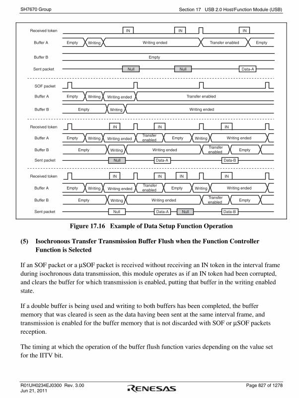
Section 17 USB 2.0 Host/Function Module (USB)
R01UH0234EJ0300 Rev. 3.00 Page 827 of 1278 Jun 21, 2011
SH7670 Group
Null Null Data-A
Null Data-BData-A
Null Null Data-BData-A
IN
IN
IN
IN
IN IN
IN
IN
IN IN
Empty
Received token
Sent packet
Buffer A
Buffer B
Received token
Sent packet
Buffer A
Buffer B
Received token
Sent packet
Buffer A
Buffer B
Empty
Empty
Empty
Empty Transfer enabled Writing ended
Transfer enabled Writing ended
Writing ended
Writing
Writing
Empty
Empty
Empty
Empty
Writing ended Writing ended
Writing ended
Writing
Writing
Writing
Writing
Transfer enabled
Transferenabled
Empty
Empty
Empty
Empty
Writing ended Writing ended
Writing ended
Writing
Writing
WritingTransferenabled
Transferenabled
SOF packet
Buffer A
Buffer B
Figure 17.16 Example of Data Setup Function Operation
(5) Isochronous Transfer Transmission Buffer Flush when the Function Controller Function is Selected
If an SOF packet or a μSOF packet is received without receiving an IN token in the interval frame during isochronous data transmission, this module operates as if an IN token had been corrupted, and clears the buffer for which transmission is enabled, putting that buffer in the writing enabled state.
If a double buffer is being used and writing to both buffers has been completed, the buffer memory that was cleared is seen as the data having been sent at the same interval frame, and transmission is enabled for the buffer memory that is not discarded with SOF or μSOF packets reception.
The timing at which the operation of the buffer flush function varies depending on the value set for the IITV bit.
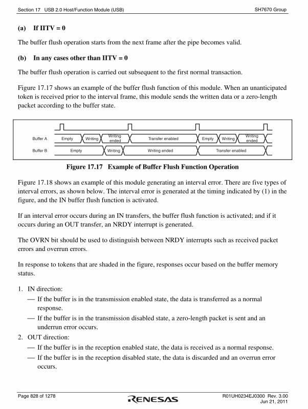
Section 17 USB 2.0 Host/Function Module (USB)
Page 828 of 1278 R01UH0234EJ0300 Rev. 3.00 Jun 21, 2011
SH7670 Group
(a) If IITV = 0
The buffer flush operation starts from the next frame after the pipe becomes valid.
(b) In any cases other than IITV = 0
The buffer flush operation is carried out subsequent to the first normal transaction.
Figure 17.17 shows an example of the buffer flush function of this module. When an unanticipated token is received prior to the interval frame, this module sends the written data or a zero-length packet according to the buffer state.
Buffer A
Buffer B
Empty
Empty
EmptyWriting ended
Writingended
Writing ended
Writing
Writing
WritingTransfer enabled
Transfer enabled
Figure 17.17 Example of Buffer Flush Function Operation
Figure 17.18 shows an example of this module generating an interval error. There are five types of interval errors, as shown below. The interval error is generated at the timing indicated by (1) in the figure, and the IN buffer flush function is activated.
If an interval error occurs during an IN transfers, the buffer flush function is activated; and if it occurs during an OUT transfer, an NRDY interrupt is generated.
The OVRN bit should be used to distinguish between NRDY interrupts such as received packet errors and overrun errors.
In response to tokens that are shaded in the figure, responses occur based on the buffer memory status.
1. IN direction:
⎯ If the buffer is in the transmission enabled state, the data is transferred as a normal response.
⎯ If the buffer is in the transmission disabled state, a zero-length packet is sent and an underrun error occurs.
2. OUT direction:
⎯ If the buffer is in the reception enabled state, the data is received as a normal response.
⎯ If the buffer is in the reception disabled state, the data is discarded and an overrun error occurs.

Section 17 USB 2.0 Host/Function Module (USB)
R01UH0234EJ0300 Rev. 3.00 Page 829 of 1278 Jun 21, 2011
SH7670 Group
Token corrupted
Packet inserted
Frame misaligned
Frame misaligned
Token delayed
Token Token
Token
Token
Token
Token
Token
Token
Token
TokenToken
Token
Token
Token
Token
Token
Token
Token
Token
Token
Token
Token
Token
1
1 1
1
1
1
1
Normal transfer
SOF
Figure 17.18 Example of an Interval Error Being Generated when IITV = 1
17.4.9 SOF Interpolation Function
When the function controller function is selected and if data could not be received at intervals of 1 ms (when using full-speed operation) or 125 μs (when using high-speed operation) because an SOF packet was corrupted or missing, this module interpolates the SOF. The SOF interpolation operation begins when the USBE and SCKE bits in SYSCFG have been set to 1 and an SOF packet is received. The interpolation function is initialized under the following conditions.
• Power-on reset
• USB bus reset
• Suspended state detected Also, the SOF interpolation operates under the following specifications.
• 125 μs/1 ms conforms to the results of the reset handshake protocol.
• The interpolation function is not activated until an SOF packet is received.
• After the first SOF packet is received, either 125 μs or 1 ms is counted with an internal clock of 48 MHz, and interpolation is carried out.
• After the second and subsequent SOF packets are received, interpolation is carried out at the previous reception interval.
• Interpolation is not carried out in the suspended state or while a USB bus reset is being received. (With suspended transitions in high-speed operation, interpolation continues for 3 ms after the last packet is received.)
This module supports the following functions based on the SOF detection. These functions also operate normally with SOF interpolation, if the SOF packet was corrupted.
• Refreshing of the frame number and the micro-frame number • SOFR interrupt timing and μSOF lock • Isochronous transfer interval count

Section 17 USB 2.0 Host/Function Module (USB)
Page 830 of 1278 R01UH0234EJ0300 Rev. 3.00 Jun 21, 2011
SH7670 Group
If an SOF packet is missing when full-speed operation is being used, the FRNM bit in FRMNUM0 is not refreshed.
If a μSOF packet is missing during high-speed operation, the UFRNM bit in FRMNUM1 is refreshed.
However, if a μSOF packet for which the μFRNM = 000 is missing, the FRNM bit is not refreshed. In this case, the FRNM bit is not refreshed even if successive μSOF packets other than μFRNM = 000 are received normally.
17.4.10 Pipe Schedule
(1) Conditions for Generating a Transaction
When the host controller function is selected and UACT has been set to 1, this module generates a transaction under the conditions noted in table 17.31.
Table 17.31 Conditions for Generating a Transaction
Conditions for Generation
Transaction DIR PID IITV0 Buffer State SUREQ
Setup ⎯*1 ⎯*1 ⎯*1 ⎯*1 1 setting
IN BUF Invalid Receive area exists
⎯*1 Control transfer data stage, status stage, bulk transfer
OUT BUF Invalid Send data exists
⎯*1
IN BUF Valid Receive area exists
⎯*1 Interrupt transfer
OUT BUF Valid Send data exists
⎯*1
IN BUF Valid *2 ⎯*1 Isochronous transfer
OUT BUF Valid *3 ⎯*1
Notes: 1. Symbols (⎯) in the table indicate that the condition is one that is unrelated to the generating of tokens. "Valid" indicates that, for interrupt transfers and isochronous transfers, the condition is generated only in transfer frames that are based on the interval counter. "Invalid" indicates that the condition is generated regardless of the interval counter.
2. This indicates that a transaction is generated regardless of whether or not there is a receive area. If there was no receive area, however, the received data is destroyed.
3. This indicates that a transaction is generated regardless of whether or not there is any data to be sent. If there was no data to be sent, however, a zero-length packet is sent.
Section 17 USB 2.0 Host/Function Module (USB)
R01UH0234EJ0300 Rev. 3.00 Page 831 of 1278 Jun 21, 2011
SH7670 Group
(2) Transfer Schedule
This section describes the transfer scheduling within a frame of this module. After the module sends an SOF, the transfer is carried out in the sequence described below.
(a) Execution of periodic transfers
A pipe is searched in the order of Pipe 1 → Pipe 2 → Pipe 6 → Pipe 7 → Pipe 8 → Pipe 9, and then, if the pipe is one for which an isochronous or interrupt transfer transaction can be generated, the transaction is generated.
(b) Setup transactions for control transfers
The DCP is checked, and if a setup transaction is possible, it is sent.
(c) Execution of bulk and control transfer data stages and status stages
A pipe is searched in the order of DCP → Pipe 1 → Pipe 2 → Pipe 3 → Pipe 4 → Pipe 5, and then, if the pipe is one for which a bulk or control transfer data stage or a control transfer status stage transaction can be generated, the transaction is generated. If a transfer is generated, processing moves to the next pipe transaction regardless of whether the response from the peripheral device is ACK or NAK. Also, if there is time for the transfer to be done within the frame, step 3 is repeated.
(3) USB Communication Enabled
Setting the UACT bit of the DVSTCTR register to 1 initiates sending of an SOF or μSOF, and makes it possible to generate a transaction.
Setting the UACT bit to 0 stops the sending of the SOF or μSOF and initiates a suspend state. If the setting of the UACT bit is changed from 1 to 0, processing stops after the next SOF or μSOF is sent.

Section 17 USB 2.0 Host/Function Module (USB)
Page 832 of 1278 R01UH0234EJ0300 Rev. 3.00 Jun 21, 2011
SH7670 Group
17.5 Usage Notes
17.5.1 Power Supplies for the USB Module
The power supply for the USB module must be turned on and off simultaneously with the other power supplies.
An example of the USB peripheral circuit that is used as the USB function is shown in figure 17.19.
VBUS100Ω
5.6 kΩ1μF
DM
1
2
3
4
DP
VBUS
GND
USB B receptable
D−
D+
REFRIN
This LSI
: to DG33: to AG33
Note :
Figure 17.19 Example of USB External Circuit when USB power supply is continuously supplied
The example of the USB external circuit when USB module is used as a host is shown in figure 17.20. The circuit to control 5 V power supply by using the port etc. is required though the detection of VBUS connection/disconnection is unnecessary for the USB host.

Section 17 USB 2.0 Host/Function Module (USB)
R01UH0234EJ0300 Rev. 3.00 Page 833 of 1278 Jun 21, 2011
SH7670 Group
VBUS100Ω
5.6kΩ1.0μF
DM
DP
VBUS
USB A receptable
D-
D+
REFRIN
This LSI
Port
3.3V 5V
120μF
0.1μF
Port
FAULT SEL
OUT
ON
OUT
GND
GND
IN
INMAX1946
1μF100kΩ
: to DG33: to AG33
Note :
Figure 17.20 Example of USB External Circuit when USB module is used as host
(1) Power-on Procedure for USB Module
Turn on the power supplies for the USB module using the following procedure.
1. Even if the USB function is not used, similar to power supplies for modules other than the USB, first turn on the 3.3-V system power supply and then turn on the 1.2-V system power supply.
2. Return the USB module to the normal operation state if it is in the module stop state. (2) Power-off Procedure for USB Module
Turn off the power supplies for the USB module using the following procedure.
1. Before turning off the power supplies for the USB module, disable USB communication by canceling pull-up of the DP pin.
2. Similar to power supplies for modules other than the USB, first turn off the 1.2-V system power supply and then turn off the 3.3-V system power supply.
Section 17 USB 2.0 Host/Function Module (USB)
Page 834 of 1278 R01UH0234EJ0300 Rev. 3.00 Jun 21, 2011
SH7670 Group
17.5.2 DTCH Interrupt
If the USB is disconnected in the host controller mode, the DTCH interrupt may be delayed for 5msec at the maximum, during which time, the NRDY interrupt may be generated.
17.5.3 Pin Treatment when USB is Not Used
Even if this USB is not used, power must be supplied to the USB power supply pins (DV33/DG33, DV12/DG12, UV12/UG12, AV33/AG33, and AV12/AG12). The VBUS pin should be tied to ground or left open. The REFRIN, DP, and DM pins should be left open. The USB_X1 pin should be pulled up and the USB_X2 pin should be left open.
17.5.4 Usage Precautions of USB Disconnection Process at the Time of Using the Function
Controller Function and Full-Speed Operations
(1) Phenomenon
When the USB detach cable at the time of receiving the host packet in the case of using the function controller function and full-speed operations for the USB module, status of DVSQ and RHST are aborted and the USB module cannot execute USB communication at the time of the USB re-attaching.
This phenomenon does not occur in the case of using the host controller function or the function controller function and high-speed operations.
(2) Occurring Conditions
The phenomenon will occur when conditions 1, 2, 3, and 4 are fulfilled at the same time.
1. USB module uses function controller function (DCFM = 0)
2. USB module full-speed operation (RHST = 010)
3. When the USB detach cable at the time of receiving the host packet.
4. When the USB D+ line pull-up is disabled (DPRPU = 1 -> 0 setting) after 3 ms from 3. [USB bus DETACH]*
Note: * USB detach is USB bus signal level, not VBINT interrupt.

Section 17 USB 2.0 Host/Function Module (USB)
R01UH0234EJ0300 Rev. 3.00 Page 835 of 1278 Jun 21, 2011
SH7670 Group
(3) Solution
When CPU detects the USB detach interruption, please process as follows.
Note: Replace DPRPU = 1 -> 0 process as follows.
1. DPRPU = 0
2. Wait for 1 μs (1000 ns)
3. DCFM = 1
4. Wait for 200 ns
5. DCFM = 0

Section 17 USB 2.0 Host/Function Module (USB)
Page 836 of 1278 R01UH0234EJ0300 Rev. 3.00 Jun 21, 2011
SH7670 Group

Section 18 SD Host Interface (SDHI)
R01UH0234EJ0300 Rev. 3.00 Page 837 of 1278 Jun 21, 2011
SH7670 Group
Section 18 SD Host Interface (SDHI)
Renesas Electronics Corporation is only able to provide information contained in this section to parties with which we have concluded a nondisclosure agreement. Please contact one of our sales representatives for details.

Section 18 SD Host Interface (SDHI)
Page 838 of 1278 R01UH0234EJ0300 Rev. 3.00 Jun 21, 2011
SH7670 Group

Section 19 I2C Bus Interface 3 (IIC3)
R01UH0234EJ0300 Rev. 3.00 Page 839 of 1278 Jun 21, 2011
SH7670 Group
Section 19 I2C Bus Interface 3 (IIC3)
The I2C bus interface 3 conforms to and provides a subset of the Philips I2C (Inter-IC) bus interface functions. However, the configuration of the registers that control the I2C bus differs partly from the Philips register configuration.
The I2C bus interface 3 has one channel.
19.1 Features
• Selection of I2C format or clocked synchronous serial format
• Continuous transmission/reception
Since the shift register, transmit data register, and receive data register are independent from each other, the continuous transmission/reception can be performed.
I2C bus format:
• Start and stop conditions generated automatically in master mode
• Selection of acknowledge output levels when receiving
• Automatic loading of acknowledge bit when transmitting
• Bit synchronization function
In master mode, the state of SCL is monitored per bit, and the timing is synchronized automatically. If transmission/reception is not yet possible, set the SCL to low until preparations are completed.
• Six interrupt sources
Transmit data empty (including slave-address match), transmit end, receive data full (including slave-address match), arbitration lost, NACK detection, and stop condition detection
• The direct memory access controller (DMAC) can be activated by a transmit-data-empty request or receive-data-full request to transfer data.
• Direct bus drive
Two pins, SCL and SDA pins, function as NMOS open-drain outputs when the bus drive function is selected.
Clocked synchronous serial format:
• Four interrupt sources
Transmit-data-empty, transmit-end, receive-data-full, and overrun error
• The direct memory access controller (DMAC) can be activated by a transmit-data-empty request or receive-data-full request to transfer data.
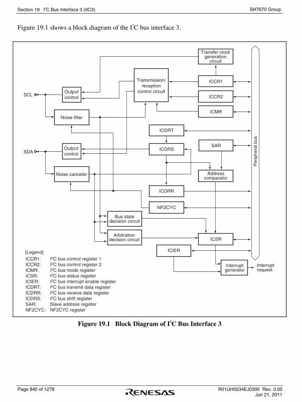
Section 19 I2C Bus Interface 3 (IIC3)
Page 840 of 1278 R01UH0234EJ0300 Rev. 3.00 Jun 21, 2011
SH7670 Group
Figure 19.1 shows a block diagram of the I2C bus interface 3.
SCL
ICCR1
ICCR2
ICMR
ICSR
ICIER
ICDRR
ICDRS
ICDRT
SARSDA
NF2CYC
Transfer clockgeneration
circuit
Addresscomparator
Interruptgenerator
Interrupt request
Bus statedecision circuit
Arbitrationdecision circuit
Noise canceler
Noise filter
Outputcontrol
Outputcontrol
Transmission/reception
control circuit
I2C bus control register 1I2C bus control register 2I2C bus mode register I2C bus status register I2C bus interrupt enable registerI2C bus transmit data register I2C bus receive data registerI2C bus shift registerSlave address registerNF2CYC register
[Legend]ICCR1:ICCR2:ICMR:ICSR:ICIER:ICDRT:ICDRR:ICDRS:SAR:NF2CYC:
Per
iphe
ral b
us
Figure 19.1 Block Diagram of I2C Bus Interface 3
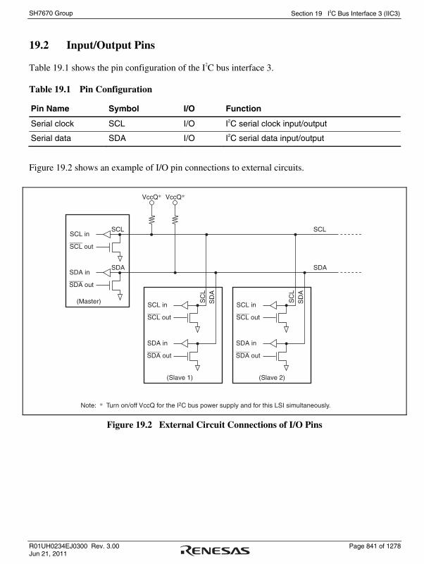
Section 19 I2C Bus Interface 3 (IIC3)
R01UH0234EJ0300 Rev. 3.00 Page 841 of 1278 Jun 21, 2011
SH7670 Group
19.2 Input/Output Pins
Table 19.1 shows the pin configuration of the I2C bus interface 3.
Table 19.1 Pin Configuration
Pin Name Symbol I/O Function
Serial clock SCL I/O I2C serial clock input/output
Serial data SDA I/O I2C serial data input/output
Figure 19.2 shows an example of I/O pin connections to external circuits.
VccQ* VccQ*
SCL in
SCL out
SCL
SDA in
SDA out
SDA
SCL
SDA
SCL in
SCL out
SC
L
SDA in
SDA out
SD
A
SCL in
SCL out
SC
L
SDA in
SDA out
SD
A
Note: * Turn on/off VccQ for the I2C bus power supply and for this LSI simultaneously.
(Master)
(Slave 1) (Slave 2)
Figure 19.2 External Circuit Connections of I/O Pins

Section 19 I2C Bus Interface 3 (IIC3)
Page 842 of 1278 R01UH0234EJ0300 Rev. 3.00 Jun 21, 2011
SH7670 Group
19.3 Register Descriptions
The I2C bus interface 3 has the following registers.
Table 19.2 Register Configuration
Channel Register Name Abbreviation R/W Initial Value Address
Access Size
I2C bus control register 1 ICCR1_0 R/W H'00 H'FFFEE000 8
I2C bus control register 2 ICCR2_0 R/W H'7D H'FFFEE001 8
I2C bus mode register ICMR_0 R/W H'38 H'FFFEE002 8
I2C bus interrupt enable register ICIER_0 R/W H'00 H'FFFEE003 8
I2C bus status register ICSR_0 R/W H'00 H'FFFEE004 8
Slave address register SAR_0 R/W H'00 H'FFFEE005 8
I2C bus transmit data register ICDRT_0 R/W H'FF H'FFFEE006 8
I2C bus receive data register ICDRR_0 R/W H'FF H'FFFEE007 8
0
NF2CYC register NF2CYC_0 R/W H'00 H'FFFEE008 8
19.3.1 I2C Bus Control Register 1 (ICCR1)
ICCR1 is an 8-bit readable/writable register that enables or disables the I2C bus interface 3, controls transmission or reception, and selects master or slave mode, transmission or reception, and transfer clock frequency in master mode.
7 6 5 4 3 2 1 0
0 0 0 0 0 0 0 0R/W R/W R/W R/W R/W R/W R/W R/W
Bit:
Initial value:R/W:
ICE RCVD MST TRS CKS[3:0]

Section 19 I2C Bus Interface 3 (IIC3)
R01UH0234EJ0300 Rev. 3.00 Page 843 of 1278 Jun 21, 2011
SH7670 Group
Bit Bit Name Initial Value R/W Description
7 ICE 0 R/W I2C Bus Interface 3 Enable
0: SCL and SDA output is disabled. (Input to SCL and SDA is enabled.)
1: This bit is enabled for transfer operations. (SCL and SDA pins are bus drive state.)
6 RCVD 0 R/W Reception Disable
Enables or disables the next operation when TRS is 0 and ICDRR is read.
0: Enables next reception
1: Disables next reception
5
4
MST
TRS
0
0
R/W
R/W
Master/Slave Select
Transmit/Receive Select
In master mode with the I2C bus format, when arbitration is lost, MST and TRS are both reset by hardware, causing a transition to slave receive mode. Modification of the TRS bit should be made between transfer frames.
When seven bits after the start condition is issued in slave receive mode match the slave address set to SAR and the 8th bit is set to 1, TRS is automatically set to 1. If an overrun error occurs in master receive mode with the clocked synchronous serial format, MST is cleared and the mode changes to slave receive mode.
Operating modes are described below according to MST and TRS combination. When clocked synchronous serial format is selected and MST = 1, clock is output.
00: Slave receive mode
01: Slave transmit mode
10: Master receive mode
11: Master transmit mode
3 to 0 CKS[3:0] 0000 R/W Transfer Clock Select
These bits should be set according to the necessary transfer rate (table 19.3) in master mode.

Section 19 I2C Bus Interface 3 (IIC3)
Page 844 of 1278 R01UH0234EJ0300 Rev. 3.00 Jun 21, 2011
SH7670 Group
Table 19.3 Transfer Rate
Bit 3 Bit 2 Bit 1 Bit 0 Transfer Rate (kHz)
CKS3 CKS2 CKS1 CKS0 Clock Pφ = 16.7 MHz
Pφ = 20.0 MHz
Pφ = 25.0 MHz
Pφ = 26.7 MHz
Pφ = 33.3 MHz
0 0 0 0 Pφ/44 379 kHz 455 kHz 568 kHz 606 kHz 758 kHz
1 Pφ/52 321 kHz 385 kHz 481 kHz 513 kHz 641 kHz
1 0 Pφ/64 260 kHz 313 kHz 391 kHz 417 kHz 521 kHz
1 Pφ/72 231 kHz 278 kHz 347 kHz 370 kHz 463 kHz
1 0 0 Pφ/84 198 kHz 238 kHz 298 kHz 317 kHz 397 kHz
1 Pφ/92 181 kHz 217 kHz 272 kHz 290 kHz 362 kHz
1 0 Pφ/100 167 kHz 200 kHz 250 kHz 267 kHz 333 kHz
1 Pφ/108 154 kHz 185 kHz 231 kHz 247 kHz 309 kHz
1 0 0 0 Pφ/176 94.7 kHz 114 kHz 142 kHz 152 kHz 189 kHz
1 Pφ/208 80.1 kHz 96.2 kHz 120 kHz 128 kHz 160 kHz
1 0 Pφ/256 65.1 kHz 78.1 kHz 97.7 kHz 104 kHz 130 kHz
1 Pφ/288 57.9 kHz 69.4 kHz 86.8 kHz 92.6 kHz 116 kHz
1 0 0 Pφ/336 49.6 kHz 59.5 kHz 74.4 kHz 79.4 kHz 99.2 kHz
1 Pφ/368 45.3 kHz 54.3 kHz 67.9 kHz 72.5 kHz 90.6 kHz
1 0 Pφ/400 41.7 kHz 50.0 kHz 62.5 kHz 66.7 kHz 83.3 kHz
1 Pφ/432 38.6 kHz 46.3 kHz 57.9 kHz 61.7 kHz 77.2 kHz
Note: The settings should satisfy external specifications.

Section 19 I2C Bus Interface 3 (IIC3)
R01UH0234EJ0300 Rev. 3.00 Page 845 of 1278 Jun 21, 2011
SH7670 Group
19.3.2 I2C Bus Control Register 2 (ICCR2)
ICCR2 is an 8-bit readable/writable register that issues start/stop conditions, manipulates the SDA pin, monitors the SCL pin, and controls reset in the control part of the I2C bus.
7 6 5 4 3 2 1 0
0 1 1 1 1 1 0 1R/W R/W R/W R/W R R R/W R
Bit:
Initial value:R/W:
BBSY SCP SDAO SDAOP SCLO - IICRST -
Bit Bit Name Initial Value R/W Description
7 BBSY 0 R/W Bus Busy
Enables to confirm whether the I2C bus is occupied or released and to issue start/stop conditions in master mode. With the clocked synchronous serial format, this bit is always read as 0. With the I2C bus format, this bit is set to 1 when the SDA level changes from high to low under the condition of SCL = high, assuming that the start condition has been issued. This bit is cleared to 0 when the SDA level changes from low to high under the condition of SCL = high, assuming that the stop condition has been issued. Write 1 to BBSY and 0 to SCP to issue a start condition. Follow this procedure when also re-transmitting a start condition. Write 0 in BBSY and 0 in SCP to issue a stop condition.
6 SCP 1 R/W Start/Stop Issue Condition Disable
Controls the issue of start/stop conditions in master mode. To issue a start condition, write 1 in BBSY and 0 in SCP. A retransmit start condition is issued in the same way. To issue a stop condition, write 0 in BBSY and 0 in SCP. This bit is always read as 1. Even if 1 is written to this bit, the data will not be stored.

Section 19 I2C Bus Interface 3 (IIC3)
Page 846 of 1278 R01UH0234EJ0300 Rev. 3.00 Jun 21, 2011
SH7670 Group
Bit Bit Name Initial Value R/W Description
5 SDAO 1 R/W SDA Output Value Control
This bit is used with SDAOP when modifying output level of SDA. This bit should not be manipulated during transfer.
0: When reading, SDA pin outputs low.
When writing, SDA pin is changed to output low.
1: When reading, SDA pin outputs high.
When writing, SDA pin is changed to output Hi-Z (outputs high by external pull-up resistance).
4 SDAOP 1 R/W SDAO Write Protect
Controls change of output level of the SDA pin by modifying the SDAO bit. To change the output level, clear SDAO and SDAOP to 0 or set SDAO to 1 and clear SDAOP to 0. This bit is always read as 1.
3 SCLO 1 R SCL Output Level
Monitors SCL output level. When SCLO is 1, SCL pin outputs high. When SCLO is 0, SCL pin outputs low.
2 ⎯ 1 R Reserved
This bit is always read as 1. The write value should always be 1.
1 IICRST 0 R/W IIC Control Part Reset
Resets the control part except for I2C registers. If this bit is set to 1 when hang-up occurs because of communication failure during I2C bus operation, some IIC3 registers and the control part can be reset.
0 ⎯ 1 R Reserved
This bit is always read as 1. The write value should always be 1.

Section 19 I2C Bus Interface 3 (IIC3)
R01UH0234EJ0300 Rev. 3.00 Page 847 of 1278 Jun 21, 2011
SH7670 Group
19.3.3 I2C Bus Mode Register (ICMR)
ICMR is an 8-bit readable/writable register that selects whether the MSB or LSB is transferred first, performs master mode wait control, and selects the transfer bit count.
Bits BC[2:0] are initialized to H'0 by the IICRST bit in ICCR2.
7 6 5 4 3 2 1 0
0 0 1 1 1 0 0 0R/W R R R R/W R/W R/W R/W
Bit:
Initial value:R/W:
MLS - - - BCWP BC[2:0]
Bit Bit Name Initial Value R/W Description
7 MLS 0 R/W MSB-First/LSB-First Select
0: MSB-first
1: LSB-first
Set this bit to 0 when the I2C bus format is used.
6 ⎯ 0 R Reserved
This bit is always read as 0. The write value should always be 0.
5, 4 ⎯ All 1 R Reserved
These bits are always read as 1. The write value should always be 1.
3 BCWP 1 R/W BC Write Protect
Controls the BC[2:0] modifications. When modifying the BC[2:0] bits, this bit should be cleared to 0. In clocked synchronous serial mode, the BC[2:0] bits should not be modified.
0: When writing, values of the BC[2:0] bits are set.
1: When reading, 1 is always read.
When writing, settings of the BC[2:0] bits are invalid.

Section 19 I2C Bus Interface 3 (IIC3)
Page 848 of 1278 R01UH0234EJ0300 Rev. 3.00 Jun 21, 2011
SH7670 Group
Bit Bit Name Initial Value R/W Description
Bit Counter
These bits specify the number of bits to be transferred next. When read, the remaining number of transfer bits is indicated. With the I2C bus format, the data is transferred with one addition acknowledge bit. Should be made between transfer frames. If these bits are set to a value other than B'000, the setting should be made while the SCL pin is low. The value returns to B'000 at the end of a data transfer, including the acknowledge bit. These bits automatically return to B'111 after a stop condition is detected.
These bits are cleared by a power-on reset and in software standby mode and module standby mode. These bits are also cleared by setting the IICRST bit of ICCR2 to 1. With the clocked synchronous serial format, these bits should not be modified.
2 to 0 BC[2:0] 000 R/W
I2C Bus Format
000: 9 bits
001: 2 bits
010: 3 bits
011: 4 bits
100: 5 bits
101: 6 bits
110: 7 bits
111: 8 bits
Clocked Synchronous Serial Format
000: 8 bits
001: 1 bit
010: 2 bits
011: 3 bits
100: 4 bits
101: 5 bits
110: 6 bits
111: 7 bits
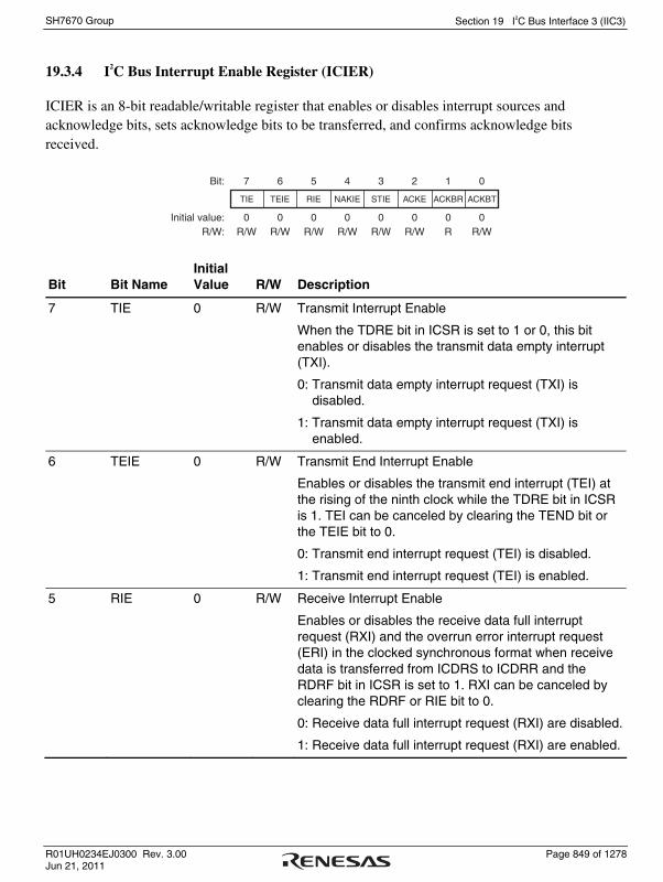
Section 19 I2C Bus Interface 3 (IIC3)
R01UH0234EJ0300 Rev. 3.00 Page 849 of 1278 Jun 21, 2011
SH7670 Group
19.3.4 I2C Bus Interrupt Enable Register (ICIER)
ICIER is an 8-bit readable/writable register that enables or disables interrupt sources and acknowledge bits, sets acknowledge bits to be transferred, and confirms acknowledge bits received.
7 6 5 4 3 2 1 0
0 0 0 0 0 0 0 0R/W R/W R/W R/W R/W R/W R R/W
Bit:
Initial value:R/W:
TIE TEIE RIE NAKIE STIE ACKE ACKBR ACKBT
Bit Bit Name Initial Value R/W Description
7 TIE 0 R/W Transmit Interrupt Enable
When the TDRE bit in ICSR is set to 1 or 0, this bit enables or disables the transmit data empty interrupt (TXI).
0: Transmit data empty interrupt request (TXI) is disabled.
1: Transmit data empty interrupt request (TXI) is enabled.
6 TEIE 0 R/W Transmit End Interrupt Enable
Enables or disables the transmit end interrupt (TEI) at the rising of the ninth clock while the TDRE bit in ICSR is 1. TEI can be canceled by clearing the TEND bit or the TEIE bit to 0.
0: Transmit end interrupt request (TEI) is disabled.
1: Transmit end interrupt request (TEI) is enabled.
5 RIE 0 R/W Receive Interrupt Enable
Enables or disables the receive data full interrupt request (RXI) and the overrun error interrupt request (ERI) in the clocked synchronous format when receive data is transferred from ICDRS to ICDRR and the RDRF bit in ICSR is set to 1. RXI can be canceled by clearing the RDRF or RIE bit to 0.
0: Receive data full interrupt request (RXI) are disabled.
1: Receive data full interrupt request (RXI) are enabled.

Section 19 I2C Bus Interface 3 (IIC3)
Page 850 of 1278 R01UH0234EJ0300 Rev. 3.00 Jun 21, 2011
SH7670 Group
Bit Bit Name Initial Value R/W Description
4 NAKIE 0 R/W NACK Receive Interrupt Enable
Enables or disables the NACK detection interrupt request (NAKI) and the overrun error (OVE set in ICSR) interrupt request (ERI) in the clocked synchronous format when the NACKF or AL/OVE bit in ICSR is set. NAKI can be canceled by clearing the NACKF, AL/OVE, or NAKIE bit to 0.
0: NACK receive interrupt request (NAKI) is disabled.
1: NACK receive interrupt request (NAKI) is enabled.
3 STIE 0 R/W Stop Condition Detection Interrupt Enable
Enables or disables the stop condition detection interrupt request (STPI) when the STOP bit in ICSR is set.
0: Stop condition detection interrupt request (STPI) is disabled.
1: Stop condition detection interrupt request (STPI) is enabled.
2 ACKE 0 R/W Acknowledge Bit Judgment Select
0: The value of the receive acknowledge bit is ignored, and continuous transfer is performed.
1: If the receive acknowledge bit is 1, continuous transfer is halted.
1 ACKBR 0 R Receive Acknowledge
In transmit mode, this bit stores the acknowledge data that are returned by the receive device. This bit cannot be modified. This bit can be canceled by setting the BBSY bit in ICCR2 to 1.
0: Receive acknowledge = 0
1: Receive acknowledge = 1
0 ACKBT 0 R/W Transmit Acknowledge
In receive mode, this bit specifies the bit to be sent at the acknowledge timing.
0: 0 is sent at the acknowledge timing.
1: 1 is sent at the acknowledge timing.

Section 19 I2C Bus Interface 3 (IIC3)
R01UH0234EJ0300 Rev. 3.00 Page 851 of 1278 Jun 21, 2011
SH7670 Group
19.3.5 I2C Bus Status Register (ICSR)
ICSR is an 8-bit readable/writable register that confirms interrupt request flags and their status.
7 6 5 4 3 2 1 0
0 0 0 0 0 0 0 0R/W R/W R/W R/W R/W R/W R/W R/W
Bit:
Initial value:R/W:
TDRE TEND RDRF NACKF STOP AL/OVE AAS ADZ
Bit Bit Name Initial Value R/W Description
7 TDRE 0 R/W Transmit Data Register Empty
[Clearing conditions]
• When 0 is written in TDRE after reading TDRE = 1
• When data is written to ICDRT
[Setting conditions]
• When data is transferred from ICDRT to ICDRS and
ICDRT becomes empty
• When TRS is set
• When the start condition (including retransmission)
is issued
• When slave mode is changed from receive mode to
transmit mode
6 TEND 0 R/W Transmit End
[Clearing conditions]
• When 0 is written in TEND after reading TEND = 1
• When data is written to ICDRT
[Setting conditions]
• When the ninth clock of SCL rises with the I2C bus
format while the TDRE flag is 1
• When the final bit of transmit frame is sent with the
clocked synchronous serial format

Section 19 I2C Bus Interface 3 (IIC3)
Page 852 of 1278 R01UH0234EJ0300 Rev. 3.00 Jun 21, 2011
SH7670 Group
Bit Bit Name Initial Value R/W Description
5 RDRF 0 R/W Receive Data Full
[Clearing conditions]
• When 0 is written in RDRF after reading RDRF = 1
• When ICDRR is read
[Setting condition]
• When a receive data is transferred from ICDRS to ICDRR
4 NACKF 0 R/W No Acknowledge Detection Flag
[Clearing condition]
• When 0 is written in NACKF after reading NACKF = 1
[Setting condition]
• When no acknowledge is detected from the receive device in transmission while the ACKE bit in ICIER is 1
3 STOP 0 R/W Stop Condition Detection Flag
[Clearing condition]
• When 0 is written in STOP after reading STOP = 1
[Setting conditions]
• When a stop condition is detected after frame
transfer is completed

Section 19 I2C Bus Interface 3 (IIC3)
R01UH0234EJ0300 Rev. 3.00 Page 853 of 1278 Jun 21, 2011
SH7670 Group
Bit Bit Name Initial Value R/W Description
2 AL/OVE 0 R/W Arbitration Lost Flag/Overrun Error Flag
Indicates that arbitration was lost in master mode with the I2C bus format and that the final bit has been received while RDRF = 1 with the clocked synchronous format.
When two or more master devices attempt to seize the bus at nearly the same time, if the I2C bus interface 3 detects data differing from the data it sent, it sets AL to 1 to indicate that the bus has been occupied by another master.
[Clearing condition]
• When 0 is written in AL/OVE after reading AL/OVE = 1
[Setting conditions]
• If the internal SDA and SDA pin disagree at the rise of SCL in master transmit mode
• When the SDA pin outputs high in master mode while a start condition is detected
• When the final bit is received with the clocked synchronous format while RDRF = 1
1 AAS 0 R/W Slave Address Recognition Flag
In slave receive mode, this flag is set to 1 if the first frame following a start condition matches bits SVA[6:0] in SAR.
[Clearing condition]
• When 0 is written in AAS after reading AAS = 1
[Setting conditions]
• When the slave address is detected in slave receive mode
• When the general call address is detected in slave receive mode.
0 ADZ 0 R/W General Call Address Recognition Flag
This bit is valid in slave receive mode with the I2C bus format.
[Clearing condition]
• When 0 is written in ADZ after reading ADZ = 1
[Setting condition]
• When the general call address is detected in slave receive mode
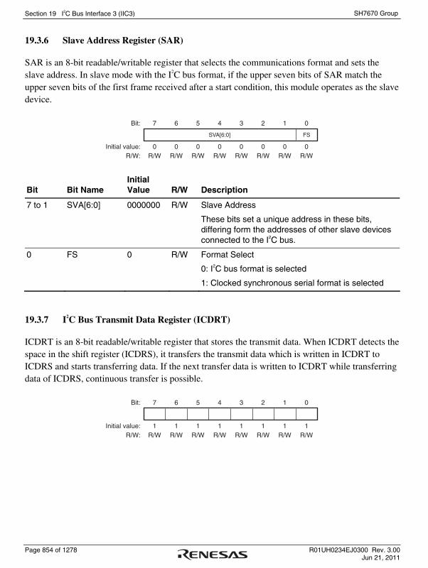
Section 19 I2C Bus Interface 3 (IIC3)
Page 854 of 1278 R01UH0234EJ0300 Rev. 3.00 Jun 21, 2011
SH7670 Group
19.3.6 Slave Address Register (SAR)
SAR is an 8-bit readable/writable register that selects the communications format and sets the slave address. In slave mode with the I2C bus format, if the upper seven bits of SAR match the upper seven bits of the first frame received after a start condition, this module operates as the slave device.
7 6 5 4 3 2 1 0
0 0 0 0 0 0 0 0R/W R/W R/W R/W R/W R/W R/W R/W
Bit:
Initial value:R/W:
SVA[6:0] FS
Bit Bit Name Initial Value R/W Description
7 to 1 SVA[6:0] 0000000 R/W Slave Address
These bits set a unique address in these bits, differing form the addresses of other slave devices connected to the I2C bus.
0 FS 0 R/W Format Select
0: I2C bus format is selected
1: Clocked synchronous serial format is selected
19.3.7 I2C Bus Transmit Data Register (ICDRT)
ICDRT is an 8-bit readable/writable register that stores the transmit data. When ICDRT detects the space in the shift register (ICDRS), it transfers the transmit data which is written in ICDRT to ICDRS and starts transferring data. If the next transfer data is written to ICDRT while transferring data of ICDRS, continuous transfer is possible.
7 6 5 4 3 2 1 0
1 1 1 1 1 1 1 1R/W R/W R/W R/W R/W R/W R/W R/W
Bit:
Initial value:R/W:

Section 19 I2C Bus Interface 3 (IIC3)
R01UH0234EJ0300 Rev. 3.00 Page 855 of 1278 Jun 21, 2011
SH7670 Group
19.3.8 I2C Bus Receive Data Register (ICDRR)
ICDRR is an 8-bit register that stores the receive data. When data of one byte is received, ICDRR transfers the receive data from ICDRS to ICDRR and the next data can be received. ICDRR is a receive-only register, therefore the CPU cannot write to this register.
7 6 5 4 3 2 1 0
1 1 1 1 1 1 1 1R R R R R R R R
Bit:
Initial value:R/W:
19.3.9 I2C Bus Shift Register (ICDRS)
ICDRS is a register that is used to transfer/receive data. In transmission, data is transferred from ICDRT to ICDRS and the data is sent from the SDA pin. In reception, data is transferred from ICDRS to ICDRR after data of one byte is received. This register cannot be read directly from the CPU.
7 6 5 4 3 2 1 0
- - - - - - - -- - - - - - - -
Bit:
Initial value:R/W:

Section 19 I2C Bus Interface 3 (IIC3)
Page 856 of 1278 R01UH0234EJ0300 Rev. 3.00 Jun 21, 2011
SH7670 Group
19.3.10 NF2CYC Register (NF2CYC)
NF2CYC is an 8-bit readable/writable register that selects the range of the noise filtering for the SCL and SDA pins. For details of the noise filter, see section 19.4.7, Noise Filter.
7 6 5 4 3 2 1 0
0 0 0 0 0 0 0 0R R R R R R R/W R/W
Bit:
Initial value:R/W:
- - - - - - PRS NF2CYC
Bit Bit Name Initial Value R/W Description
7 to 2 ⎯ All 0 R Reserved
These bits are always read as 0. The write value should always be 0.
1 PRS 0 R/W Pulse Width Ratio Select
Specifies the ratio of the high-level period to the low-level period for the SCL signal.
0: The ratio of high to low is 0.5 to 0.5.
1: The ratio of high to low is about 0.4 to 0.6.
0 NF2CYC 0 R/W Noise Filtering Range Select
0: The noise less than one cycle of the peripheral clock
can be filtered out
1: The noise less than two cycles of the peripheral clock
can be filtered out
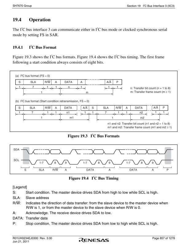
Section 19 I2C Bus Interface 3 (IIC3)
R01UH0234EJ0300 Rev. 3.00 Page 857 of 1278 Jun 21, 2011
SH7670 Group
19.4 Operation
The I2C bus interface 3 can communicate either in I2C bus mode or clocked synchronous serial mode by setting FS in SAR.
19.4.1 I2C Bus Format
Figure 19.3 shows the I2C bus formats. Figure 19.4 shows the I2C bus timing. The first frame following a start condition always consists of eight bits.
S ASLA
7 n
R/W DATA A
1
1 m
1 11
A/A
1
P
1
S SLA
7 n1 7
R/W A DATA
1 1
1 m1
1
A/A
1
S
1
SLA R/W
1
1 m2
A
1
DATA
n2
A/A
1
P
1
(a) I2C bus format (FS = 0)
(b) I2C bus format (Start condition retransmission, FS = 0)
n: Transfer bit count (n = 1 to 8)m: Transfer frame count (m ≥ 1)
n1 and n2: Transfer bit count (n1 and n2 = 1 to 8)m1 and m2: Transfer frame count (m1 and m2 ≥ 1)
Figure 19.3 I2C Bus Formats
SDA
SCL
S SLA R/W A
981-7 981-7 981-7
DATA A DATA A P
Figure 19.4 I2C Bus Timing
[Legend]
S: Start condition. The master device drives SDA from high to low while SCL is high.
SLA: Slave address R/W: Indicates the direction of data transfer: from the slave device to the master device when
R/W is 1, or from the master device to the slave device when R/W is 0. A: Acknowledge. The receive device drives SDA to low.
DATA: Transfer data
P: Stop condition. The master device drives SDA from low to high while SCL is high.

Section 19 I2C Bus Interface 3 (IIC3)
Page 858 of 1278 R01UH0234EJ0300 Rev. 3.00 Jun 21, 2011
SH7670 Group
19.4.2 Master Transmit Operation
In master transmit mode, the master device outputs the transmit clock and transmit data, and the slave device returns an acknowledge signal. For master transmit mode operation timing, refer to figures 19.5 and 19.6. The transmission procedure and operations in master transmit mode are described below.
1. Set the ICE bit in ICCR1 to 1. Also, set bits CKS[3:0] in ICCR1. (Initial setting)
2. Read the BBSY flag in ICCR2 to confirm that the bus is released. Set the MST and TRS bits in ICCR1 to select master transmit mode. Then, write 1 to BBSY and 0 to SCP. (Start condition issued) This generates the start condition.
3. After confirming that TDRE in ICSR has been set, write the transmit data (the first byte data show the slave address and R/W) to ICDRT. At this time, TDRE is automatically cleared to 0, and data is transferred from ICDRT to ICDRS. TDRE is set again.
4. When transmission of one byte data is completed while TDRE is 1, TEND in ICSR is set to 1 at the rise of the 9th transmit clock pulse. Read the ACKBR bit in ICIER, and confirm that the slave device has been selected. Then, write second byte data to ICDRT. When ACKBR is 1, the slave device has not been acknowledged, so issue the stop condition. To issue the stop condition, write 0 to BBSY and SCP. SCL is fixed low until the transmit data is prepared or the stop condition is issued.
5. The transmit data after the second byte is written to ICDRT every time TDRE is set.
6. Write the number of bytes to be transmitted to ICDRT. Wait until TEND is set (the end of last byte data transmission) while TDRE is 1, or wait for NACK (NACKF in ICSR = 1) from the receive device while ACKE in ICIER is 1. Then, issue the stop condition to clear TEND or NACKF.
7. When the STOP bit in ICSR is set to 1, the operation returns to the slave receive mode.
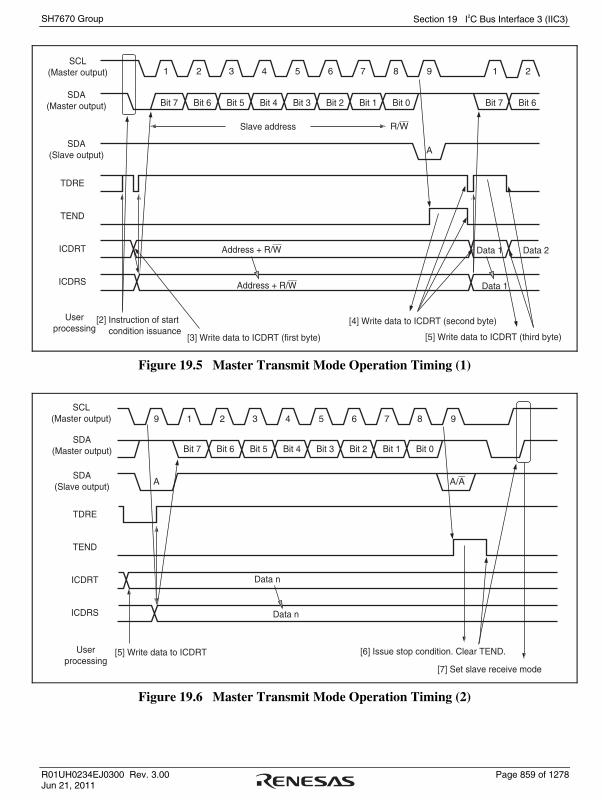
Section 19 I2C Bus Interface 3 (IIC3)
R01UH0234EJ0300 Rev. 3.00 Page 859 of 1278 Jun 21, 2011
SH7670 Group
TDRE
TEND
ICDRT
ICDRS
1 2 1 23 4 5 6 7 8 9
A
R/W
SCL(Master output)
SDA(Master output)
SDA(Slave output)
[5] Write data to ICDRT (third byte)
[2] Instruction of start condition issuance
[3] Write data to ICDRT (first byte)
[4] Write data to ICDRT (second byte)Userprocessing
Bit 7
Slave address
Address + R/W Data 1
Data 1
Data 2
Address + R/W
Bit 6 Bit 7 Bit 6Bit 5 Bit 4 Bit 3 Bit 2 Bit 1 Bit 0
Figure 19.5 Master Transmit Mode Operation Timing (1)
TDRE
TEND
ICDRT
ICDRS
19 2 3 4 5 6 7 8 9
A A/A
[6] Issue stop condition. Clear TEND.
[7] Set slave receive mode
SCL(Master output)
SDA(Master output)
SDA(Slave output)
Bit 7 Bit 6
Data n
Data n
Bit 5 Bit 4 Bit 3 Bit 2 Bit 1 Bit 0
[5] Write data to ICDRTUserprocessing
Figure 19.6 Master Transmit Mode Operation Timing (2)

Section 19 I2C Bus Interface 3 (IIC3)
Page 860 of 1278 R01UH0234EJ0300 Rev. 3.00 Jun 21, 2011
SH7670 Group
19.4.3 Master Receive Operation
In master receive mode, the master device outputs the receive clock, receives data from the slave device, and returns an acknowledge signal. For master receive mode operation timing, refer to figures 19.7 and 19.8. The reception procedure and operations in master receive mode are shown below.
1. Clear the TEND bit in ICSR to 0, then clear the TRS bit in ICCR1 to 0 to switch from master transmit mode to master receive mode. Then, clear the TDRE bit to 0.
2. When ICDRR is read (dummy data read), reception is started, and the receive clock is output, and data received, in synchronization with the internal clock. The master device outputs the level specified by ACKBT in ICIER to SDA, at the 9th receive clock pulse.
3. After the reception of first frame data is completed, the RDRF bit in ICSR is set to 1 at the rise of 9th receive clock pulse. At this time, the receive data is read by reading ICDRR, and RDRF is cleared to 0.
4. The continuous reception is performed by reading ICDRR every time RDRF is set. If 8th receive clock pulse falls after reading ICDRR by the other processing while RDRF is 1, SCL is fixed low until ICDRR is read.
5. If next frame is the last receive data, set the RCVD bit in ICCR1 to 1 before reading ICDRR. This enables the issuance of the stop condition after the next reception.
6. When the RDRF bit is set to 1 at rise of the 9th receive clock pulse, issue the stage condition.
7. When the STOP bit in ICSR is set to 1, read ICDRR. Then clear the RCVD bit to 0.
8. The operation returns to the slave receive mode. Note: If only one byte is received, read ICDRR (dummy-read) after the RCVD bit in ICCR1 is
set.

Section 19 I2C Bus Interface 3 (IIC3)
R01UH0234EJ0300 Rev. 3.00 Page 861 of 1278 Jun 21, 2011
SH7670 Group
TDRE
TEND
ICDRS
ICDRR
1
A
2 13 4 5 6 7 8 99
A
TRS
RDRF
[1] Clear TDRE after clearing TEND and TRS
[2] Read ICDRR (dummy read) [3] Read ICDRR
SCL(Master output)
SDA(Master output)
SDA(Slave output) Bit 7
Master transmit mode Master receive mode
Bit 7Bit 6 Bit 5 Bit 4 Bit 3 Bit 2 Bit 1 Bit 0
Userprocessing
Data 1
Data 1
Figure 19.7 Master Receive Mode Operation Timing (1)
RDRF
RCVD
ICDRS
ICDRR
19 2 3 4 5 6 7 8 9
A A/A
Data n-1 Data n
Data nData n-1
[5] Read ICDRR after setting RCVD [6] Issue stop condition
[7] Read ICDRR, and clear RCVD [8] Set slave
receive mode
SCL(Master output)
SDA(Master output)
SDA(Slave output)
Bit 7 Bit 6 Bit 5 Bit 4 Bit 3 Bit 2 Bit 1 Bit 0
Userprocessing
Figure 19.8 Master Receive Mode Operation Timing (2)

Section 19 I2C Bus Interface 3 (IIC3)
Page 862 of 1278 R01UH0234EJ0300 Rev. 3.00 Jun 21, 2011
SH7670 Group
19.4.4 Slave Transmit Operation
In slave transmit mode, the slave device outputs the transmit data, while the master device outputs the receive clock and returns an acknowledge signal. For slave transmit mode operation timing, refer to figures 19.9 and 19.10.
The transmission procedure and operations in slave transmit mode are described below.
1. Set the ICE bit in ICCR1 to 1. Set bits CKS[3:0] in ICCR1. (Initial setting) Set the MST and TRS bits in ICCR1 to select slave receive mode, and wait until the slave address matches.
2. When the slave address matches in the first frame following detection of the start condition, the slave device outputs the level specified by ACKBT in ICIER to SDA, at the rise of the 9th clock pulse. At this time, if the 8th bit data (R/W) is 1, the TRS bit in ICCR1 and the TDRE bit in ICSR are set to 1, and the mode changes to slave transmit mode automatically. The continuous transmission is performed by writing transmit data to ICDRT every time TDRE is set.
3. If TDRE is set after writing last transmit data to ICDRT, wait until TEND in ICSR is set to 1, with TDRE = 1. When TEND is set, clear TEND.
4. Clear TRS for the end processing, and read ICDRR (dummy read). SCL is opened.
5. Clear TDRE.

Section 19 I2C Bus Interface 3 (IIC3)
R01UH0234EJ0300 Rev. 3.00 Page 863 of 1278 Jun 21, 2011
SH7670 Group
TDRE
TEND
ICDRS
ICDRR
1
A
2 13 4 5 6 7 8 99
A
TRS
ICDRT
SCL(Master output)
Slave receive mode
Slave transmit mode
SDA(Master output)
SDA(Slave output)
SCL(Slave output)
Bit 7 Bit 7
Data 1
Data 1
Data 2 Data 3
Data 2
Bit 6 Bit 5 Bit 4 Bit 3 Bit 2 Bit 1 Bit 0
[2] Write data to ICDRT (data 1) [2] Write data to ICDRT (data 2) [2] Write data to ICDRT (data 3)Userprocessing
Figure 19.9 Slave Transmit Mode Operation Timing (1)

Section 19 I2C Bus Interface 3 (IIC3)
Page 864 of 1278 R01UH0234EJ0300 Rev. 3.00 Jun 21, 2011
SH7670 Group
TDRE
TEND
ICDRS
ICDRR
19 2 3 4 5 6 7 8 9
TRS
ICDRT
A A
Data n
SCL(Master output)
SDA(Master output)
SDA(Slave output)
SCL(Slave output)
Bit 7
Slave transmit mode
Slave receivemode
Bit 6 Bit 5 Bit 4 Bit 3 Bit 2 Bit 1 Bit 0
[3] Clear TEND [5] Clear TDRE [4] Read ICDRR (dummy read) after clearing TRS
Userprocessing
Figure 19.10 Slave Transmit Mode Operation Timing (2)

Section 19 I2C Bus Interface 3 (IIC3)
R01UH0234EJ0300 Rev. 3.00 Page 865 of 1278 Jun 21, 2011
SH7670 Group
19.4.5 Slave Receive Operation
In slave receive mode, the master device outputs the transmit clock and transmit data, and the slave device returns an acknowledge signal. For slave receive mode operation timing, refer to figures 19.11 and 19.12. The reception procedure and operations in slave receive mode are described below.
1. Set the ICE bit in ICCR1 to 1. Set bits CKS[3:0] in ICCR1. (Initial setting) Set the MST and TRS bits in ICCR1 to select slave receive mode, and wait until the slave address matches.
2. When the slave address matches in the first frame following detection of the start condition, the slave device outputs the level specified by ACKBT in ICIER to SDA, at the rise of the 9th clock pulse. At the same time, RDRF in ICSR is set to read ICDRR (dummy read). (Since the read data show the slave address and R/W, it is not used.)
3. Read ICDRR every time RDRF is set. If 8th receive clock pulse falls while RDRF is 1, SCL is fixed low until ICDRR is read. The change of the acknowledge before reading ICDRR, to be returned to the master device, is reflected to the next transmit frame.
4. The last byte data is read by reading ICDRR.
ICDRS
ICDRR
1 2 13 4 5 6 7 8 99
AA
RDRF
Data 1 Data 2
Data 1
SCL(Master output)
SDA(Master output)
SDA(Slave output)
SCL(Slave output)
Bit 7 Bit 7Bit 6 Bit 5 Bit 4 Bit 3 Bit 2 Bit 1 Bit 0
[2] Read ICDRR (dummy read) [2] Read ICDRRUserprocessing
Figure 19.11 Slave Receive Mode Operation Timing (1)

Section 19 I2C Bus Interface 3 (IIC3)
Page 866 of 1278 R01UH0234EJ0300 Rev. 3.00 Jun 21, 2011
SH7670 Group
ICDRS
ICDRR
1 2 3 4 5 6 7 8 99
AA
RDRF
SCL(Master output)
SDA(Master output)
SDA(Slave output)
SCL(Slave output)
Userprocessing
Bit 7 Bit 6 Bit 5 Bit 4 Bit 3 Bit 2 Bit 1 Bit 0
Data 1
[3] Set ACKBT [3] Read ICDRR [4] Read ICDRR
Data 2
Data 1
Figure 19.12 Slave Receive Mode Operation Timing (2)
19.4.6 Clocked Synchronous Serial Format
This module can be operated with the clocked synchronous serial format, by setting the FS bit in SAR to 1. When the MST bit in ICCR1 is 1, the transfer clock output from SCL is selected. When MST is 0, the external clock input is selected.
(1) Data Transfer Format
Figure 19.13 shows the clocked synchronous serial transfer format.
The transfer data is output from the fall to the fall of the SCL clock, and the data at the rising edge of the SCL clock is guaranteed. The MLS bit in ICMR sets the order of data transfer, in either the MSB first or LSB first. The output level of SDA can be changed during the transfer wait, by the SDAO bit in ICCR2.
SDA
SCL
Bit 0 Bit 1 Bit 2 Bit 3 Bit 4 Bit 5 Bit 6 Bit 7
Figure 19.13 Clocked Synchronous Serial Transfer Format
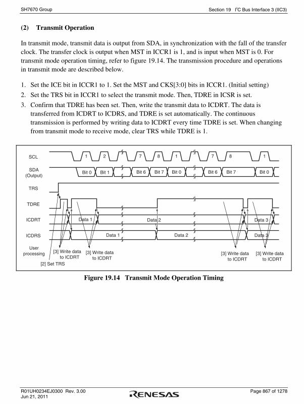
Section 19 I2C Bus Interface 3 (IIC3)
R01UH0234EJ0300 Rev. 3.00 Page 867 of 1278 Jun 21, 2011
SH7670 Group
(2) Transmit Operation
In transmit mode, transmit data is output from SDA, in synchronization with the fall of the transfer clock. The transfer clock is output when MST in ICCR1 is 1, and is input when MST is 0. For transmit mode operation timing, refer to figure 19.14. The transmission procedure and operations in transmit mode are described below.
1. Set the ICE bit in ICCR1 to 1. Set the MST and CKS[3:0] bits in ICCR1. (Initial setting)
2. Set the TRS bit in ICCR1 to select the transmit mode. Then, TDRE in ICSR is set.
3. Confirm that TDRE has been set. Then, write the transmit data to ICDRT. The data is transferred from ICDRT to ICDRS, and TDRE is set automatically. The continuous transmission is performed by writing data to ICDRT every time TDRE is set. When changing from transmit mode to receive mode, clear TRS while TDRE is 1.
1 2 7 8 1 7 8 1SCL
TRS
TDRE
ICDRT
ICDRS
Bit 0
Data 1
Data 1
Data 2 Data 3
Data 3Data 2
Bit 6 Bit 7 Bit 0 Bit 6 Bit 7 Bit 0Bit 1SDA(Output)
Userprocessing [3] Write data
to ICDRT[3] Write data to ICDRT
[3] Write data to ICDRT
[3] Write data to ICDRT
[2] Set TRS
Figure 19.14 Transmit Mode Operation Timing

Section 19 I2C Bus Interface 3 (IIC3)
Page 868 of 1278 R01UH0234EJ0300 Rev. 3.00 Jun 21, 2011
SH7670 Group
(3) Receive Operation
In receive mode, data is latched at the rise of the transfer clock. The transfer clock is output when MST in ICCR1 is 1, and is input when MST is 0. For receive mode operation timing, refer to figure 19.15. The reception procedure and operations in receive mode are described below.
1. Set the ICE bit in ICCR1 to 1. Set bits CKS[3:0] in ICCR1. (Initial setting)
2. When the transfer clock is output, set MST to 1 to start outputting the receive clock.
3. When the receive operation is completed, data is transferred from ICDRS to ICDRR and RDRF in ICSR is set. When MST = 1, the next byte can be received, so the clock is continually output. The continuous reception is performed by reading ICDRR every time RDRF is set. When the 8th clock is risen while RDRF is 1, the overrun is detected and AL/OVE in ICSR is set. At this time, the previous reception data is retained in ICDRR.
4. To stop receiving when MST = 1, set RCVD in ICCR1 to 1, then read ICDRR. Then, SCL is fixed high after receiving the next byte data.
Notes: Follow the steps below to receive only one byte with MST = 1 specified. See figure 19.16
for the operation timing.
1. Set the ICE bit in ICCR1 to 1. Set bits CKS[3:0] in ICCR1. (Initial setting)
2. Set MST = 1 while the RCVD bit in ICCR1 is 0. This causes the receive clock to be output.
3. Check if the BC2 bit in ICMR is set to 1 and then set the RCVD bit in ICCR1 to 1. This causes the SCL to be fixed to the high level after outputting one byte of the receive clock.

Section 19 I2C Bus Interface 3 (IIC3)
R01UH0234EJ0300 Rev. 3.00 Page 869 of 1278 Jun 21, 2011
SH7670 Group
1 2 7 8 1 7 8 1 2SCL
MST
TRS
RDRF
ICDRS
ICDRR
SDA(Input)
Bit 0 Bit 6 Bit 7 Bit 0 Bit 6 Bit 7 Bit 0 Bit 1Bit 1
Userprocessing
Data 1
Data 1
Data 2
Data 2
Data 3
[2] Set MST (when outputting the clock)
[3] Read ICDRR [3] Read ICDRR
Figure 19.15 Receive Mode Operation Timing
1 2 3 4 5 6 7 8
000
SCL
MST
RCVD
111 110 101 100 011 010 001 000
SDA(Input)
Bit 0 Bit 1 Bit 2 Bit 3 Bit 4 Bit 5 Bit 6 Bit 7
BC2 to BC0
[2] Set MST [3] Set the RCVD bit after checking if BC2 = 1
Figure 19.16 Operation Timing For Receiving One Byte (MST = 1)

Section 19 I2C Bus Interface 3 (IIC3)
Page 870 of 1278 R01UH0234EJ0300 Rev. 3.00 Jun 21, 2011
SH7670 Group
19.4.7 Noise Filter
The logic levels at the SCL and SDA pins are routed through noise filters before being latched internally. Figure 19.17 shows a block diagram of the noise filter circuit.
The noise filter consists of three cascaded latches and a match detector. The SCL (or SDA) input signal is sampled on the peripheral clock. When NF2CYC is set to 0, this signal is not passed forward to the next circuit unless the outputs of both latches agree. When NF2CYC is set to 1, this signal is not passed forward to the next circuit unless the outputs of three latches agree. If they do not agree, the previous value is held.
CQD
CQD
CQ
1
0
D
NF2CYC
SCL or SDAinput signal
InternalSCL or SDAsignal
Sampling clock
Samplingclock
Peripheral clockcycle
Latch Latch Match detector
Latch
Match detector
Figure 19.17 Block Diagram of Noise Filter

Section 19 I2C Bus Interface 3 (IIC3)
R01UH0234EJ0300 Rev. 3.00 Page 871 of 1278 Jun 21, 2011
SH7670 Group
19.4.8 Example of Use
Flowcharts in respective modes that use the I2C bus interface 3 are shown in figures 19.18 to 19.21.
BBSY=0 ?No
TEND=1 ?No
Yes
Start
[1]
[2]
[3]
[4]
[5]
[6]
[7]
[8]
[9]
[10]
[11]
[13]
[14]
[15]
Initialize
Set MST and TRSin ICCR1 to 1
Write 1 to BBSYand 0 to SCP
Write transmit datain ICDRT
Write 0 to BBSY and SCP
Set MST and TRSin ICCR1 to 0
Read BBSY in ICCR2
Read TEND in ICSR
Read ACKBR in ICIER
Master receive mode
Yes
ACKBR=0 ?
Write transmit data in ICDRT
Read TDRE in ICSR
Read TEND in ICSR
Clear TEND in ICSR
Read STOP in ICSR
Clear TDRE in ICSR
End
Write transmit data in ICDRT
Transmitmode?
No
Yes
TDRE=1 ?
Last byte?
STOP=1 ?
No
No
No
No
No
Yes
Yes
TEND=1 ?
Yes
Yes
Yes
[1] Test the status of the SCL and SDA lines.
[2] Set master transmit mode.
[3] Issue the start condition.
[4] Set the first byte (slave address + R/W) of transmit data.
[5] Wait for 1 byte to be transmitted.
[6] Test the acknowledge transferred from the specified slave device.
[7] Set the second and subsequent bytes (except for the final byte) of transmit data.
[8] Wait for ICDRT empty.
[9] Set the last byte of transmit data.
[10] Wait for last byte to be transmitted.
[11] Clear the TEND flag.
[12] Clear the STOP flag.
[13] Issue the stop condition.
[14] Wait for the creation of stop condition.
[15] Set slave receive mode. Clear TDRE.
[12]Clear STOP in ICSR
Figure 19.18 Sample Flowchart for Master Transmit Mode

Section 19 I2C Bus Interface 3 (IIC3)
Page 872 of 1278 R01UH0234EJ0300 Rev. 3.00 Jun 21, 2011
SH7670 Group
[10]
No
Yes
RDRF=1 ?No
Yes
RDRF=1 ?
Last receive- 1?
Master receive mode
Clear TEND in ICSR
Set TRS in ICCR1 to 0
Clear TDRE in ICSR
Set ACKBT in ICIER to 0
Dummy-read ICDRR
Read RDRF in ICSR
Read ICDRR
Set ACKBT in ICIER to 1
Set RCVD in ICCR1 to 0
Read ICDRR
Read RDRF in ICSR
Write 0 to BBSYand SCP
Read STOP in ICSR
Read ICDRR
Clear RCVD in ICCR1 to 0
Set MST in ICCR1 to 0
End
No
Yes
STOP=1 ?No
Yes
[1] Clear TEND, select master receive mode, and then clear TDRE. *1
[2] Set acknowledge to the transmit device. *1
[3] Dummy-read ICDDR. *1
[4] Wait for 1 byte to be received. *2
[5] Check whether it is the (last receive - 1). *2
[6] Read the receive data.
[7] Set acknowledge of the final byte. Disable continuous reception (RCVD = 1). *2
[8] Read the (final byte - 1) of received data.
[9] Wait for the last byte to be receive.
[10] Clear the STOP flag.
[11] Issue the stop condition.
[12] Wait for the creation of stop condition.
[13] Read the last byte of receive data.
[14] Clear RCVD.
[15] Set slave receive mode.
[1]
[2]
[3]
[4]
[5]
[6]
[7]
[8]
[9]
[11]
[12]
[13]
[14]
[15]
Notes: 1. Make sure that no interrupt will be generated during steps [1] to [3]. 2. At last receive - 1 (when (5) is satisfied), ensure that no interrupt occurs during the processing of (4), (5), or (7).
Supplementary information
When the size of receive data is only one byte in reception, steps [2] to [6] are skipped after step [1], before jumping to step [7]. The step [8] is dummy-read in ICDRR.
Clear STOP in ICSR
Figure 19.19 Sample Flowchart for Master Receive Mode

Section 19 I2C Bus Interface 3 (IIC3)
R01UH0234EJ0300 Rev. 3.00 Page 873 of 1278 Jun 21, 2011
SH7670 Group
TDRE=1 ?
Yes
Yes
No
Slave transmit mode
Clear AAS in ICSR
Write transmit datain ICDRT
Read TDRE in ICSR
Lastbyte?
Write transmit datain ICDRT
Read TEND in ICSR
Clear TEND in ICSR
Set TRS in ICCR1 to 0
Dummy-read ICDRR
Clear TDRE in ICSR
End
[1] Clear the AAS flag.
[2] Set transmit data for ICDRT (except for the last byte).
[3] Wait for ICDRT empty.
[4] Set the last byte of transmit data.
[5] Wait for the last byte to be transmitted.
[6] Clear the TEND flag.
[7] Set slave receive mode.
[8] Dummy-read ICDRR to release the SCL.
[9] Clear the TDRE flag.
No
No
Yes
TEND=1 ?
[1]
[2]
[3]
[4]
[5]
[6]
[7]
[8]
[9]
Figure 19.20 Sample Flowchart for Slave Transmit Mode
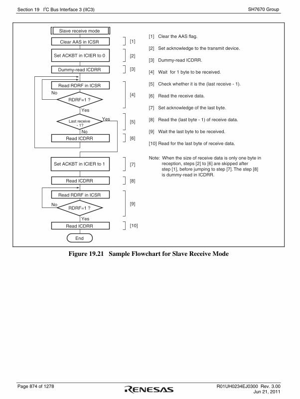
Section 19 I2C Bus Interface 3 (IIC3)
Page 874 of 1278 R01UH0234EJ0300 Rev. 3.00 Jun 21, 2011
SH7670 Group
No
Yes
RDRF=1 ?No
Yes
RDRF=1 ?
Last receive - 1?
Slave receive mode
Clear AAS in ICSR
Set ACKBT in ICIER to 0
Dummy-read ICDRR
Read RDRF in ICSR
Read ICDRR
Set ACKBT in ICIER to 1
Read ICDRR
Read RDRF in ICSR
Read ICDRR
End
No
Yes
[1]
[2]
[3]
[4]
[5]
[6]
[7]
[8]
[9]
[10]
[1] Clear the AAS flag.
[2] Set acknowledge to the transmit device.
[3] Dummy-read ICDRR.
[4] Wait for 1 byte to be received.
[5] Check whether it is the (last receive - 1).
[6] Read the receive data.
[7] Set acknowledge of the last byte.
[8] Read the (last byte - 1) of receive data.
[9] Wait the last byte to be received.
[10] Read for the last byte of receive data.
Note: When the size of receive data is only one byte in reception, steps [2] to [6] are skipped after step [1], before jumping to step [7]. The step [8] is dummy-read in ICDRR.
Figure 19.21 Sample Flowchart for Slave Receive Mode

Section 19 I2C Bus Interface 3 (IIC3)
R01UH0234EJ0300 Rev. 3.00 Page 875 of 1278 Jun 21, 2011
SH7670 Group
19.5 Interrupt Requests
There are six interrupt requests in this module; transmit data empty, transmit end, receive data full, NACK detection, STOP recognition, and arbitration lost/overrun error. Table 19.4 shows the contents of each interrupt request.
Table 19.4 Interrupt Requests
Interrupt Request Abbreviation Interrupt Condition I2C Bus Format
Clocked Synchronous Serial Format
Transmit data Empty TXI (TDRE = 1) • (TIE = 1) √ √
Transmit end TEI (TEND = 1) • (TEIE = 1) √ √
Receive data full RXI (RDRF = 1) • (RIE = 1) √ √
STOP recognition STPI (STOP = 1) • (STIE = 1) √ ⎯
NACK detection √ ⎯
Arbitration lost/ overrun error
NAKI {(NACKF = 1) + (AL = 1)} • (NAKIE = 1) √ √
When the interrupt condition described in table 19.4 is 1, the CPU executes an interrupt exception handling. Note that a TXI or RXI interrupt can activate the DMAC if the setting for DMAC activation has been made. In such a case, an interrupt request is not sent to the CPU. Interrupt sources should be cleared in the exception handling. The TDRE and TEND bits are automatically cleared to 0 by writing the transmit data to ICDRT. The RDRF bit is automatically cleared to 0 by reading ICDRR. The TDRE bit is set to 1 again at the same time when the transmit data is written to ICDRT. Therefore, when the TDRE bit is cleared to 0, then an excessive data of one byte may be transmitted.
Section 19 I2C Bus Interface 3 (IIC3)
Page 876 of 1278 R01UH0234EJ0300 Rev. 3.00 Jun 21, 2011
SH7670 Group
19.6 Bit Synchronous Circuit
In master mode, this module has a possibility that high level period may be short in the two states described below.
• When SCL is driven to low by the slave device
• When the rising speed of SCL is lowered by the load of the SCL line (load capacitance or pull-up resistance)
Therefore, it monitors SCL and communicates by bit with synchronization.
Figure 19.22 shows the timing of the bit synchronous circuit and table 19.5 shows the time when the SCL output changes from low to Hi-Z then SCL is monitored.
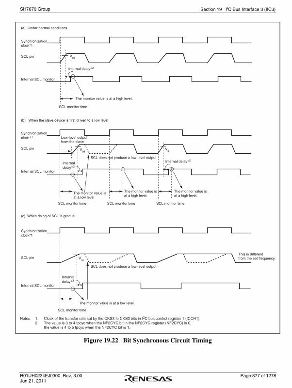
Section 19 I2C Bus Interface 3 (IIC3)
R01UH0234EJ0300 Rev. 3.00 Page 877 of 1278 Jun 21, 2011
SH7670 Group
Synchronization clock*1
SCL pin
Internal SCL monitor
Synchronization clock*1
SCL pin
Internal SCL monitor
Synchronization clock*1
SCL pin
Internal SCL monitor
VIH
Internal delay*2
Internal delay*2
The monitor value is at a low level.
SCL does not produce a low-level output.
SCL does not produce a low-level output.
SCL monitor time
VIH
Internal delay*2
VIH
The monitor value is at a low level.
The monitor value isat a high level.
SCL monitor time SCL monitor time SCL monitor time
This is different from the set frequency.
Low-level output from the slave
The monitor value is at a high level.
Internal delay*2
VIH
SCL monitor time
The monitor value is at a high level.
Notes: 1. Clock of the transfer rate set by the CKS3 to CKS0 bits in I2C bus control register 1 (ICCR1) 2. The value is 3 to 4 tpcyc when the NF2CYC bit in the NF2CYC register (NF2CYC) is 0; the value is 4 to 5 tpcyc when the NF2CYC bit is 1.
(a) Under normal conditions
(b) When the slave device is first driven to a low level
(c) When rising of SCL is gradual
Figure 19.22 Bit Synchronous Circuit Timing
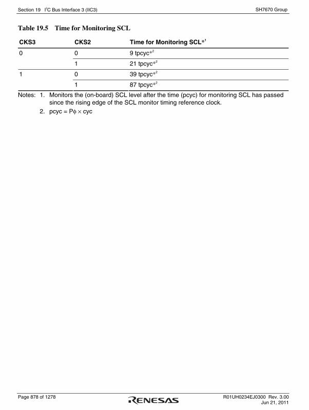
Section 19 I2C Bus Interface 3 (IIC3)
Page 878 of 1278 R01UH0234EJ0300 Rev. 3.00 Jun 21, 2011
SH7670 Group
Table 19.5 Time for Monitoring SCL
CKS3 CKS2 Time for Monitoring SCL*1
0 9 tpcyc*2 0
1 21 tpcyc*2
0 39 tpcyc*2 1
1 87 tpcyc*2
Notes: 1. Monitors the (on-board) SCL level after the time (pcyc) for monitoring SCL has passed since the rising edge of the SCL monitor timing reference clock.
2. pcyc = Pφ × cyc

Section 19 I2C Bus Interface 3 (IIC3)
R01UH0234EJ0300 Rev. 3.00 Page 879 of 1278 Jun 21, 2011
SH7670 Group
19.7 Usage Notes
19.7.1 Notes on Working in Multi-master Mode
When working in multi-master mode, if the setting for the transfer route of the LSI (CKS3 to CKS0 in ICCR1) is lower than that for any other master, an SCL with an unexpected width may be output occasionally.
The transfer rate that is set here must be at least 1/1.8 times the highest transfer rate of the other masters.
19.7.2 Notes on Working in Master Receive Mode
If the ICDRR is read near the falling edge of the eighth clock, no receive data may be captured.
If RCVD = 1 is set near the falling edge of the eighth clock when the receive buffer is full, no stop conditions may be issued.
Use either of the following methods.
1. In master receive mode, reading the ICDRR should be performed before the falling edge of the eighth is detected.
2. In master receive mode, RCVD = 1 should be set so that processing proceeds on a per-byte basis.
19.7.3 Notes on Setting ACKBT in Master Receive Mode
When working in master receive mode, the ACKBT should be set before the eighth SCL in the final data being transferred continuously starts falling. Otherwise, the slave’s sending device might overrun.

Section 19 I2C Bus Interface 3 (IIC3)
Page 880 of 1278 R01UH0234EJ0300 Rev. 3.00 Jun 21, 2011
SH7670 Group
19.7.4 Notes on the States of MST and TRN Bits when Arbitration Is Lost
If the multi-master is used and the MST and TRS bits are operated sequentially to assign the master send setting, a conflict may occur as seen in the combination of AL = 1 in ICSR and master transmit mode (MST = 1 and TRS = 1), depending on the timing when arbitration is lost while the bit manipulation instruction in the TRS is being executed.
The following methods can be used to avoid this phenomenon.
• When working in multi-master mode, use the MOV instruction to set the MST and TRS.
• If arbitration is lost, confirm the MST = 0 and TRS = 0 settings.
If any settings other than MST = 0 and TRS = 0 are found, the MST = 0 and TRS = 0 settings must be performed again.
19.7.5 Note Regarding Master Receive Mode of I2C-Bus Interface Mode
(1) Note
When stop condition generation or start condition regeneration overlaps with the falling edge of the ninth clock cycle of the SCL signal, an additional cycle is output after the ninth clock cycle.
(2) Countermeasure
After a master receive operation is completed, confirm the falling edge of the ninth clock cycle of the SCL signal and generate a stop condition or regenerate a start condition.
Confirm the falling edge of the ninth clock cycle of the SCL signal as follows: Confirm the SCLO bit in the ICCR2 register (SCL monitor flag) becomes 0 (SCL pin is low) after confirming the RDRF bit in the ICSR register (receive data register full flag) becomes 1.

Section 19 I2C Bus Interface 3 (IIC3)
R01UH0234EJ0300 Rev. 3.00 Page 881 of 1278 Jun 21, 2011
SH7670 Group
19.7.6 Accessing ICE and IICRST during I2C Bus Operation
(1) Problem
When 0 is written to ICE in ICCR1 or 1 is written to IICRST in ICCR2 during I2C bus operation, the values of BBSY in ICCR2 and STOP in ICSR become undefined.
(2) Conditions
The above problem occurs when 0 is written to ICE in ICCR1 or 1 is written to IICRST in ICCR2 when any of conditions 1 to 4 below is satisfied.
1. In master transmit mode (MST = 1 and TRS = 1 in ICCR1), when the IIC3 module holds access rights to the I2C bus.
2. In master receive mode (MST = 1 and TRS = 0 in ICCR1), when the IIC3 module holds access rights to the I2C bus.
3. In slave transmit mode (MST = 0 and TRS = 1 in ICCR1), when the IIC3 module is performing a data transmit operation.
4. In slave receive mode (MST = 0 and TRS = 0 in ICCR1), when the IIC3 module is transmitting an acknowledge signal.
(3) Workarounds
The undefined state of BBSY in ICCR2 can be canceled by using one of the following workarounds.
• BBSY is set to 1 when a start condition (SCL is high-level and SDA falling edge) is input.
• BBSY is cleared to 0 when an end condition (SCL is high-level and SDA rising edge) is input.
• In master transmit mode, write 1 to BBSY and 0 to SCP in ICCR2 while SCL and SDA are both high-level to generate a start condition. BBSY is set to 1 when a start condition (SCL is high-level and SDA falling edge) is output.
• In master transmit mode or master receive mode, when SDA is low-level and there is no device other than the IIC2 or IIC3 module to drive SCL low, write 0 to BBSY and SCP in ICCR2 to generate an end condition. BBSY is cleared to 0 when an end condition (SCL is high-level and SDA rising edge) is output.
• Writing 1 to FS in SAR causes BBSY to be cleared to 0.

Section 19 I2C Bus Interface 3 (IIC3)
Page 882 of 1278 R01UH0234EJ0300 Rev. 3.00 Jun 21, 2011
SH7670 Group
(4) Supplemental Description of Register Functions
Using IICRST for register initialization
• Writing 1 to IICRST in ICCR2 causes SDAO and SCLO in ICCR2 to be set to 1.
• In master transmit mode or slave transmit mode, writing 1 to IICRST causes TDRE in ICSR to be set to 1.
• During a reset interval triggered by setting IICRST to 1, write access to BBSY, SCP, and SDAO in ICCR2 is disabled.
• Writing 1 to IICRST does not clear the BBSY bit in ICCR2 to 0. However, depending on the states of pins SCL and SDA, an end condition (SCL is high-level and SDA rising edge) may occur, resulting in BBSY being cleared to 0. In addition, there may be similar effects on other bits as well.
• During a reset interval triggered by setting IICRST to 1, data reception and transmission halts. However, the functions that detect start conditions, end conditions, and bus arbitration lost conditions are active. This means that the states of ICCR1, ICCR2, and ICSR may be updated, depending on the signals input to SCL and SDA.

Section 20 Host Interface (HIF)
R01UH0234EJ0300 Rev. 3.00 Page 883 of 1278 Jun 21, 2011
SH7670 Group
Section 20 Host Interface (HIF)
This LSI incorporates a host interface (HIF) for use in high-speed transfer of data between external devices which cannot utilize the system bus.
The HIF allows external devices to read from and write to 4 Kbytes (2 Kbytes × 2 banks) of the on-chip RAM exclusively for HIF use (HIFRAM) within this LSI, in 32-bit units. Interrupts issued to this LSI by an external device, interrupts sent from this LSI to the external device, and DMA transfer requests sent from this LSI to the external device are also supported. By using HIFRAM and these interrupt functions, software-based data transfer between external devices and this LSI becomes possible, and connection to external devices not releasing bus mastership is enabled.
Using HIFRAM, the HIF also supports HIF boot mode allowing this LSI to be booted.
20.1 Features
The HIF has the following features.
• An external device can read from or write to HIFRAM in 32-bit units via the HIF pins (access in 8-bit or 16-bit units not allowed). The on-chip CPU can read from or write to HIFRAM in 8-bit, 16-bit, or 32-bit units, via the internal peripheral bus. The HIFRAM access mode can be specified as bank mode or non-bank mode.
• When an external device accesses HIFRAM via the HIF pins, automatic increment of addresses and the endian can be specified with the HIF internal registers.
• By writing to specific bits in the HIF internal registers from an external device, or by accessing the end address of HIFRAM from the external device, interrupts (internal interrupts) can be issued to the on-chip CPU. Conversely, by writing to specific bits in the HIF internal registers from the on-chip CPU, interrupts (external interrupts) or DMAC transfer requests can be sent from the on-chip CPU to the external device.
• There are seven interrupt source bits each for internal interrupts and external interrupts. Accordingly, software control of 128 different interrupts is possible, enabling high-speed data transfer using interrupts.
• In HIF boot mode, this LSI can be booted from HIFRAM by an external device storing the instruction code in HIFRAM.

Section 20 Host Interface (HIF)
Page 884 of 1278 R01UH0234EJ0300 Rev. 3.00 Jun 21, 2011
SH7670 Group
Figure 20.1 shows a block diagram of the HIF.
HIF
SC
R
HIF
DAT
A
HIF
IICR
HIF
MC
R
HIF
EIC
R
HIF
BC
R
HIF
AD
RH
IFD
TR
HIF
BIC
R
HIF
IDX
HIF
GS
R
HIFCS
HIFRS
HIFWR
HIFRD
HIFMD
HIFINT
HIFDREQ
HIFD15 to HIFD00
HIF
HIFRDY
HIFEBL
HIFI
HIFBI
Select
HIFRAM
Control circuitIn
tern
al b
us
[Legend]HIF index registerHIF general status registerHIF status/control registerHIF memory control registerHIF internal interrupt control registerHIF external interrupt control register
HIFIDX:HIFGSR:HIFSCR:HIFMCR:HIFIICR:HIFEICR:
HIF address registerHIF data registerHIF boot control registerHIFDREQ trigger registerHIF bank interrupt control registerHIF interrupt (internal interrupt)HIF bank interrupt (internal interrupt)
HIFADR:HIFDATA:HIFBCR:HIFDTR:HIFBICR:HIFI:HIFIB:
HIFRAM
Figure 20.1 Block Diagram of HIF

Section 20 Host Interface (HIF)
R01UH0234EJ0300 Rev. 3.00 Page 885 of 1278 Jun 21, 2011
SH7670 Group
20.2 Input/Output Pins
Table 20.1 shows the HIF pin configuration.
Table 20.1 Pin Configuration
Name Abbreviation I/O Description
HIF data pins HIFD15 to HIFD00 I/O Address, data, or command input/output to the HIF
HIF chip select HIFCS Input Chip select input to the HIF
HIF register select HIFRS Input Switching between HIF access types
0: Normal access (other than below)
1: Index register write
HIF write HIFWR Input Write strobe signal. Low level is input when an external device writes data to the HIF.
HIF read HIFRD Input Read strobe signal. Low level is input when an external device reads data from the HIF.
HIF interrupt HIFINT Output Interrupt request to an external device from the HIF
HIF mode HIFMD Input Selects whether or not this LSI is started up in HIF boot mode. If a power-on reset is canceled when high level is input, this LSI is started up in HIF boot mode.
HIFDMAC transfer request
HIFDREQ Output To an external device, DMAC transfer request with HIFRAM as the destination
HIF boot ready HIFRDY Output Indicates that the HIF reset is canceled in this LSI and access from an external device to the HIF can be accepted.
After 20 clock cycles (max.) of the peripheral clock following negate of the reset input pin of this LSI, this pin is asserted.
HIF pin enable HIFEBL Input All HIF pins other than this pin are asserted by high-level input.

Section 20 Host Interface (HIF)
Page 886 of 1278 R01UH0234EJ0300 Rev. 3.00 Jun 21, 2011
SH7670 Group
20.3 Parallel Access
20.3.1 Operation
The HIF can be accessed by combining the HIFCS, HIFRS, HIFWR, and HIFRD pins. Table 20.2 shows the correspondence between combinations of these signals and HIF operations.
Table 20.2 HIF Operations
HIFCS HIFRS HIFWR HIFRD Operation
1 * * * No operation (NOP)
0 1 0 1 Write to index register (HIFIDX[7:0])
0 0 0 1 Write to register specified by HIFIDX[7:0]
0 0 1 0 Read from register specified by HIFIDX[7:0]
0 * 1 1 No operation (NOP)
0 * 0 0 Setting prohibited
[Legend]
*: Don't care
20.3.2 Connection Method
When connecting the HIF to an external device, a method like that shown in figure 20.2 should be used.
External device
CS
A02
WR
RD
D15 to D00
HIF
HIFCS
HIFRS
HIFWR
HIFRD
HIFD15 to HIFD00
Figure 20.2 HIF Connection Example

Section 20 Host Interface (HIF)
R01UH0234EJ0300 Rev. 3.00 Page 887 of 1278 Jun 21, 2011
SH7670 Group
20.4 Register Descriptions
The HIF has the following registers.
• HIF index register (HIFIDX)
• HIF general status register (HIFGSR)
• HIF status/control register (HIFSCR)
• HIF memory control register (HIFMCR)
• HIF internal interrupt control register (HIFIICR)
• HIF external interrupt control register (HIFEICR)
• HIF address register (HIFADR)
• HIF data register (HIFDATA)
• HIF boot control register (HIFBCR)
• HIFDREQ trigger register (HIFDTR)
• HIF bank interrupt control register (HIFBICR)

Section 20 Host Interface (HIF)
Page 888 of 1278 R01UH0234EJ0300 Rev. 3.00 Jun 21, 2011
SH7670 Group
20.4.1 HIF Index Register (HIFIDX)
HIFIDX is a 32-bit register used to specify the register read from or written to by an external device when the HIFRS pin is held low. HIFIDX can be only read by the on-chip CPU. HIFIDX can be only written to by an external device while the HIFRS pin is driven high.
31 30 29 28 27 26 25 24 23 22 21 20 19 18 17 16Bit:
Initial Value:R/W:
Bit:
Initial Value:R/W:
15 14 13 12 11 10 9 8 7 6 5 4 3 2 1 0
0 0 0 0 0 0 0 0 0 0 0 0 0 0 0 0R R R R R R R R R R R R R R R R
0 0 0 0 0 0 0 0 0 0 0 0 0 0 0 0R R R R R R R R R/W R/W R/W R/W R/W R/W R/W R/W
⎯ ⎯ ⎯ ⎯ ⎯ ⎯ ⎯ ⎯ ⎯
⎯ ⎯ ⎯ REG5
⎯ ⎯ ⎯ ⎯ ⎯ ⎯ ⎯
⎯ ⎯ ⎯ ⎯ ⎯ REG4 REG3 REG2 REG1 REG0 BYTE1 BYTE0
Bit Bit Name Initial Value R/W Description
31 to 8 ⎯ All 0 R Reserved
These bits are always read as 0. The write value should always be 0.
7
6
5
4
3
2
REG5
REG4
REG3
REG2
REG1
REG0
0
0
0
0
0
0
R/W
R/W
R/W
R/W
R/W
R/W
HIF Internal Register Select
These bits specify which register among HIFGSR, HIFSCR, HIFMCR, HIFIICR, HIFEICR, HIFADR, HIFDATA, and HIFBCR is accessed by an external device.
000000: HIFGSR
000001: HIFSCR
000010: HIFMCR
000011: HIFIICR
000100: HIFEICR
000101: HIFADR
000110: HIFDATA
001111: HIFBCR
Other than above: Setting prohibited
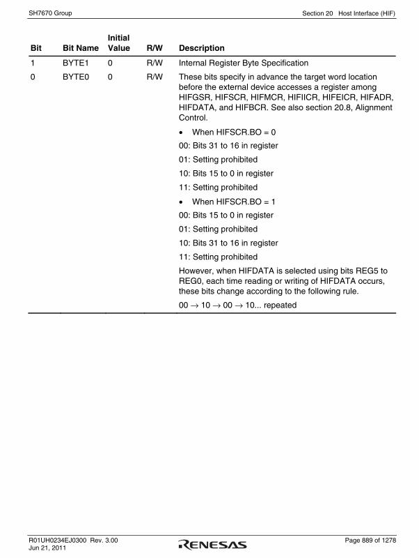
Section 20 Host Interface (HIF)
R01UH0234EJ0300 Rev. 3.00 Page 889 of 1278 Jun 21, 2011
SH7670 Group
Bit Bit Name Initial Value R/W Description
1
0
BYTE1
BYTE0
0
0
R/W
R/W
Internal Register Byte Specification
These bits specify in advance the target word location before the external device accesses a register among HIFGSR, HIFSCR, HIFMCR, HIFIICR, HIFEICR, HIFADR, HIFDATA, and HIFBCR. See also section 20.8, Alignment Control.
• When HIFSCR.BO = 0
00: Bits 31 to 16 in register
01: Setting prohibited
10: Bits 15 to 0 in register
11: Setting prohibited
• When HIFSCR.BO = 1
00: Bits 15 to 0 in register
01: Setting prohibited
10: Bits 31 to 16 in register
11: Setting prohibited
However, when HIFDATA is selected using bits REG5 to REG0, each time reading or writing of HIFDATA occurs, these bits change according to the following rule.
00 → 10 → 00 → 10... repeated
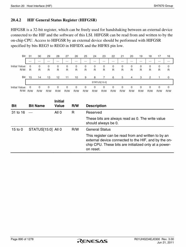
Section 20 Host Interface (HIF)
Page 890 of 1278 R01UH0234EJ0300 Rev. 3.00 Jun 21, 2011
SH7670 Group
20.4.2 HIF General Status Register (HIFGSR)
HIFGSR is a 32-bit register, which can be freely used for handshaking between an external device connected to the HIF and the software of this LSI. HIFGSR can be read from and written to by the on-chip CPU. Access to HIFGSR by an external device should be performed with HIFGSR specified by bits REG5 to REG0 in HIFIDX and the HIFRS pin low.
31 30 29 28 27 26 25 24 23 22 21 20 19 18 17 16Bit:
Initial Value:R/W:
Bit:
Initial Value:R/W:
15 14 13 12 11 10 9 8 7 6 5 4 3 2 1 0
0 0 0 0 0 0 0 0 0 0 0 0 0 0 0 0R R R R R R R R R R R R R R R R
0 0 0 0 0 0 0 0 0 0 0 0 0 0 0 0R/W R/W R/W R/W R/W R/W R/W R/W R/W R/W R/W R/W R/W R/W R/W R/W
⎯ ⎯ ⎯ ⎯ ⎯ ⎯ ⎯ ⎯ ⎯
STATUS[15:0]
⎯ ⎯ ⎯ ⎯ ⎯ ⎯ ⎯
Bit Bit Name Initial Value R/W Description
31 to 16 ⎯ All 0 R Reserved
These bits are always read as 0. The write value should always be 0.
15 to 0 STATUS[15:0] All 0 R/W General Status
This register can be read from and written to by an external device connected to the HIF, and by the on-chip CPU. These bits are initialized only at a power-on reset.

Section 20 Host Interface (HIF)
R01UH0234EJ0300 Rev. 3.00 Page 891 of 1278 Jun 21, 2011
SH7670 Group
20.4.3 HIF Status/Control Register (HIFSCR)
HIFSCR is a 32-bit register used to control the HIFRAM access mode and endian setting. HIFSCR can be read from and written to by the on-chip CPU. Access to HIFSCR by an external device should be performed with HIFSCR specified by bits REG5 to REG0 in HIFIDX and the HIFRS pin low.
31 30 29 28 27 26 25 24 23 22 21 20 19 18 17 16Bit:
Initial Value:R/W:
Bit:
Initial Value:R/W:
15 14 13 12 11 10 9 8 7 6 5 4 3 2 1 0
0 0 0 0 0 0 0 0 0 0 0 0 0 0 0 0R R R R R R R R R R R R R R R R
0 0 0 0 0 0 0 0 0 1 0/1 0 0 0 0 0R R R R R/W R/W R/W R/W R R R R R R/W R/W R/W
⎯ ⎯ ⎯ ⎯ ⎯ ⎯ ⎯ ⎯ ⎯
DPOL BMD BSEL ⎯
⎯ ⎯ ⎯ ⎯ ⎯ ⎯ ⎯
⎯ ⎯ ⎯ ⎯ DMD ⎯ MD1 ⎯ ⎯ WBSWP EDN BO
Bit Bit Name Initial Value R/W Description
31 to 12 ⎯ All 0 R Reserved
These bits are always read as 0. The write value should always be 0.
11
10
DMD
DPOL
0
0
R/W
R/W
DREQ Mode
DREQ Polarity
Controls the assert mode for the HIFDREQ pin. For details on the negate timing, see section 20.7, External DMAC Interface.
00: For a DMAC transfer request to an external device, low level is generated at the HIFDREQ pin. The default for the HIFDREQ pin is high-level output.
01: For a DMAC transfer request to an external device, high level is generated at the HIFDREQ pin. The default for the HIFDREQ pin is low-level output.
10: For a DMAC transfer request to an external device, falling edge is generated at the HIFDREQ pin. The default for the HIFDREQ pin is high-level output.
11: For a DMAC transfer request to an external device, rising edge is generated at the HIFDREQ pin. The default for the HIFDREQ pin is low-level output.

Section 20 Host Interface (HIF)
Page 892 of 1278 R01UH0234EJ0300 Rev. 3.00 Jun 21, 2011
SH7670 Group
Bit Bit Name Initial Value R/W Description
9
8
BMD
BSEL
0
0
R/W
R/W
HIFRAM Bank Mode
HIFRAM Bank Select
Controls the HIFRAM access mode.
00: Both an external device and the on-chip CPU can access bank 0. When access by both of these conflict, even though the access addresses differ, access by the external device is processed before access by the on-chip CPU. Bank 1 cannot be accessed.
01: Both an external device and the on-chip CPU can access bank 1. When access by both of these conflict, even though the access addresses differ, access by the external device is processed before access by the on-chip CPU. Bank 0 cannot be accessed.
10: An external device can access only bank 0 while the on-chip CPU can access only bank 1.
11: An external device can access only bank 1 while the on-chip CPU can access only bank 0.
7 ⎯ 0 R Reserved
This bit is always read as 0. The write value should always be 0.
6 ⎯ 1 R Reserved
This bit is always read as 1. The write value should always be 1.
5 MD1 0/1 R HIF Mode 1
Indicates whether this LSI was started up in HIF boot mode or non-HIF boot mode. This bit stores the value of the HIFMD pin sampled at a power-on reset
0: Started up in non-HIF boot mode (booted from the memory connected to area 0)
1: Started up in HIF boot mode (booted from HIFRAM)
4, 3 ⎯ All 0 R Reserved
These bits are always read as 0. The write value should always be 0.
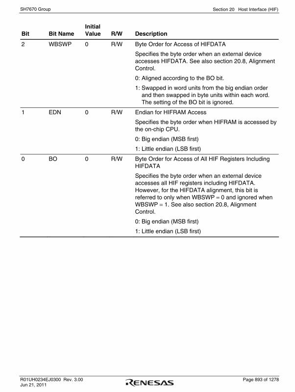
Section 20 Host Interface (HIF)
R01UH0234EJ0300 Rev. 3.00 Page 893 of 1278 Jun 21, 2011
SH7670 Group
Bit Bit Name Initial Value R/W Description
2 WBSWP 0 R/W Byte Order for Access of HIFDATA
Specifies the byte order when an external device accesses HIFDATA. See also section 20.8, Alignment Control.
0: Aligned according to the BO bit.
1: Swapped in word units from the big endian order and then swapped in byte units within each word. The setting of the BO bit is ignored.
1 EDN 0 R/W Endian for HIFRAM Access
Specifies the byte order when HIFRAM is accessed by the on-chip CPU.
0: Big endian (MSB first)
1: Little endian (LSB first)
0 BO 0 R/W Byte Order for Access of All HIF Registers Including HIFDATA
Specifies the byte order when an external device accesses all HIF registers including HIFDATA. However, for the HIFDATA alignment, this bit is referred to only when WBSWP = 0 and ignored when WBSWP = 1. See also section 20.8, Alignment Control.
0: Big endian (MSB first)
1: Little endian (LSB first)

Section 20 Host Interface (HIF)
Page 894 of 1278 R01UH0234EJ0300 Rev. 3.00 Jun 21, 2011
SH7670 Group
20.4.4 HIF Memory Control Register (HIFMCR)
HIFMCR is a 32-bit register used to control HIFRAM. HIFMCR can be only read by the on-chip CPU. Access to HIFMCR by an external device should be performed with HIFMCR specified by bits REG5 to REG0 in HIFIDX and the HIFRS pin low.
31 30 29 28 27 26 25 24 23 22 21 20 19 18 17 16Bit:
Initial Value:R/W:
Bit:
Initial Value:R/W:
15 14 13 12 11 10 9 8 7 6 5 4 3 2 1 0
0 0 0 0 0 0 0 0 0 0 0 0 0 0 0 0R R R R R R R R R R R R R R R R
0 0 0 0 0 0 0 0 0 0 0 0 0 0 0 0R R R R R R R R R/W* R R/W* R
Note: * Changing the HIFRAM banks accessible from an external device by setting the BMD and BSEL bits in HIFSCR does not affect the setting of this bit.
R/W* R R R/W*
⎯ ⎯ ⎯ ⎯ ⎯ ⎯ ⎯ ⎯ ⎯
⎯ ⎯ ⎯ LOCK
⎯ ⎯ ⎯ ⎯ ⎯ ⎯ ⎯
⎯ ⎯ ⎯ ⎯ ⎯ ⎯ WT ⎯ RD ⎯ ⎯ AI/AD
Bit Bit Name Initial Value R/W Description
31 to 8 ⎯ All 0 R Reserved
These bits are always read as 0. The write value should always be 0.
7 LOCK 0 R/W* Lock
This bit is used to lock the access direction (read or write) for consecutive access of HIFRAM by an external device via HIFDATA. When this bit is set to 1, the values of the RD and WT bits set at the same time are held until this bit is next cleared to 0. When the RD bit and this bit are simultaneously set to 1, consecutive read mode is entered. When the WT bit and this bit are simultaneously set to 1, consecutive write mode is entered. Both the RD and WT bits should not be set to 1 simultaneously.
6 ⎯ 0 R Reserved
This bit is always read as 0. The write value should always be 0.

Section 20 Host Interface (HIF)
R01UH0234EJ0300 Rev. 3.00 Page 895 of 1278 Jun 21, 2011
SH7670 Group
Bit Bit Name Initial Value R/W Description
5 WT 0 R/W* Write
When this bit is set to 1, the HIFDATA value is written to the HIFRAM position corresponding to HIFADR.
If this bit and the LOCK bit are set to 1 simultaneously, HIFRAM consecutive write mode is entered, and high-speed data transfer becomes possible. This mode is maintained until this bit is next cleared to 0, or until the LOCK bit is cleared to 0.
If the LOCK bit is not simultaneously set to 1 with this bit, writing to HIFRAM is performed only once. Thereafter, the value of this bit is automatically cleared to 0.
4 ⎯ 0 R Reserved
This bit is always read as 0. The write value should always be 0.
3 RD 0 R/W* Read
When this bit is set to 1, the HIFRAM data corresponding to HIFADR is fetched to HIFDATA.
If this bit and the LOCK bit are set to 1 simultaneously, HIFRAM consecutive read mode is entered, and high-speed data transfer becomes possible. This mode is maintained until this bit is next cleared to 0, or until the LOCK bit is cleared to 0.
If the LOCK bit is not simultaneously set to 1 with this bit, reading of HIFRAM is performed only once. Thereafter, the value of this bit is automatically cleared to 0.
2, 1 ⎯ All 0 R Reserved
These bits are always read as 0. The write value should always be 0.
0 AI/AD 0 R/W* Address Auto-Increment/Decrement
This bit is valid only when the LOCK bit is 1. The value of HIFADR is automatically incremented by 4 or decremented by 4 according to the setting of this bit each time reading or writing of HIFRAM is performed.
0: Auto-increment mode (+4)
1: Auto-decrement mode (−4)
Note: * Changing the HIFRAM banks accessible from an external device by setting the BMD and BSEL bits in HIFSCR does not affect the setting of this bit.
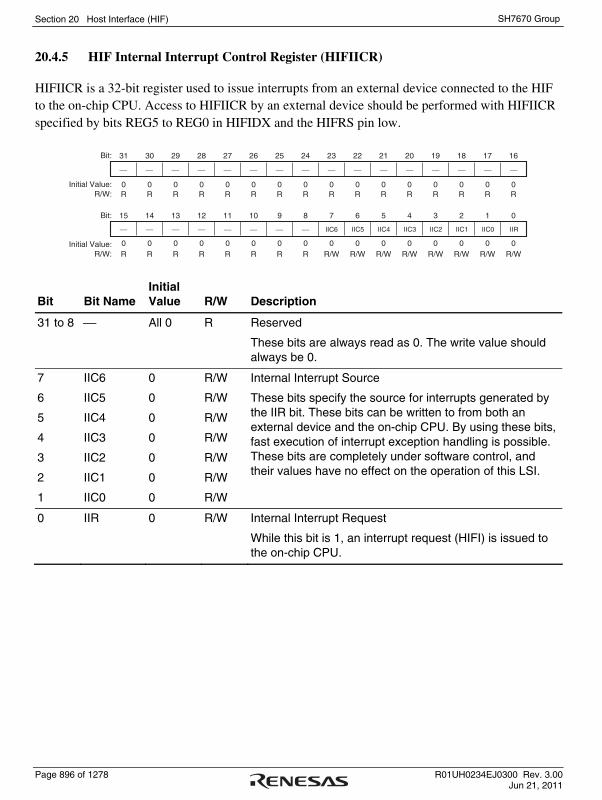
Section 20 Host Interface (HIF)
Page 896 of 1278 R01UH0234EJ0300 Rev. 3.00 Jun 21, 2011
SH7670 Group
20.4.5 HIF Internal Interrupt Control Register (HIFIICR)
HIFIICR is a 32-bit register used to issue interrupts from an external device connected to the HIF to the on-chip CPU. Access to HIFIICR by an external device should be performed with HIFIICR specified by bits REG5 to REG0 in HIFIDX and the HIFRS pin low.
31 30 29 28 27 26 25 24 23 22 21 20 19 18 17 16Bit:
Initial Value:R/W:
Bit:
Initial Value:R/W:
15 14 13 12 11 10 9 8 7 6 5 4 3 2 1 0
0 0 0 0 0 0 0 0 0 0 0 0 0 0 0 0R R R R R R R R R R R R R R R R
0 0 0 0 0 0 0 0 0 0 0 0 0 0 0 0R R R R R R R R R/W R/W R/W R/W R/W R/W R/W R/W
⎯ ⎯ ⎯ ⎯ ⎯ ⎯ ⎯ ⎯ ⎯
⎯ ⎯ ⎯ IIC6
⎯ ⎯ ⎯ ⎯ ⎯ ⎯ ⎯
⎯ ⎯ ⎯ ⎯ ⎯ IIC5 IIC4 IIC3 IIC2 IIC1 IIC0 IIR
Bit Bit Name Initial Value R/W Description
31 to 8 ⎯ All 0 R Reserved
These bits are always read as 0. The write value should always be 0.
7
6
5
4
3
2
1
IIC6
IIC5
IIC4
IIC3
IIC2
IIC1
IIC0
0
0
0
0
0
0
0
R/W
R/W
R/W
R/W
R/W
R/W
R/W
Internal Interrupt Source
These bits specify the source for interrupts generated by the IIR bit. These bits can be written to from both an external device and the on-chip CPU. By using these bits, fast execution of interrupt exception handling is possible. These bits are completely under software control, and their values have no effect on the operation of this LSI.
0 IIR 0 R/W Internal Interrupt Request
While this bit is 1, an interrupt request (HIFI) is issued to the on-chip CPU.

Section 20 Host Interface (HIF)
R01UH0234EJ0300 Rev. 3.00 Page 897 of 1278 Jun 21, 2011
SH7670 Group
20.4.6 HIF External Interrupt Control Register (HIFEICR)
HIFEICR is a 32-bit register used to issue interrupts to an external device connected to the HIF from this LSI. Access to HIFEICR by an external device should be performed with HIFEICR specified by bits REG5 to REG0 in HIFIDX and the HIFRS pin low.
31 30 29 28 27 26 25 24 23 22 21 20 19 18 17 16Bit:
Initial Value:R/W:
15 14 13 12 11 10 9 8 7 6 5 4 3 2 1 0
0 0 0 0 0 0 0 0 0 0 0 0 0 0 0 0R R R R R R R R R R R R R R R R
0 0 0 0 0 0 0 0 0 0 0 0 0 0 0 0R R R R R R R R R/W R/W R/W R/W R/W R/W R/W R/W
⎯ ⎯ ⎯ ⎯ ⎯ ⎯ ⎯ ⎯ ⎯
⎯ ⎯ ⎯ EIC6
⎯ ⎯ ⎯ ⎯ ⎯ ⎯ ⎯
⎯ ⎯ ⎯ ⎯ ⎯ EIC5 EIC4 EIC3 EIC2 EIC1 EIC0 EIR
Bit:
Initial Value:R/W:
Bit Bit Name Initial Value R/W Description
31 to 8 ⎯ All 0 R Reserved
These bits are always read as 0. The write value should always be 0.
7
6
5
4
3
2
1
EIC6
EIC5
EIC4
EIC3
EIC2
EIC1
EIC0
0
0
0
0
0
0
0
R/W
R/W
R/W
R/W
R/W
R/W
R/W
External Interrupt Source
These bits specify the source for interrupts generated by the EIR bit. These bits can be written to from both an external device and the on-chip CPU. By using these bits, fast execution of interrupt exception handling is possible. These bits are completely under software control, and their values have no effect on the operation of this LSI.
0 EIR 0 R/W External Interrupt Request
While this bit is 1, the HIFINT pin is asserted to issue an interrupt request to an external device from this LSI.

Section 20 Host Interface (HIF)
Page 898 of 1278 R01UH0234EJ0300 Rev. 3.00 Jun 21, 2011
SH7670 Group
20.4.7 HIF Address Register (HIFADR)
HIFADR is a 32-bit register which indicates the address in HIFRAM to be accessed by an external device. When using the LOCK bit setting in HIFMCR to specify consecutive access of HIFRAM, auto-increment (+4) or auto-decrement (-4) of the address, according to the AI/AD bit setting in HIFMCR, is performed automatically, and HIFADR is updated. HIFADR can be only read by the on-chip CPU. Access to HIFADR by an external device should be performed with HIFADR specified by bits REG5 to REG0 in HIFIDX and the HIFRS pin low.
31 30 29 28 27 26 25 24 23 22 21 20 19 18 17 16Bit:
Initial Value:R/W:
Bit:
Initial Value:R/W:
15 14 13 12 11 10 9 8 7 6 5 4 3 2 1 0
0 0 0 0 0 0 0 0 0 0 0 0 0 0 0 0R R R R R R R R R R R R R R R R
0 0 0 0 0 0 0 0 0 0 0 0 0 0 0 0R R R R R R/W R/W R/W R/W R/W R/W R/W R/W R/W R R
⎯ ⎯ ⎯ ⎯ ⎯ ⎯ ⎯ ⎯ ⎯ ⎯ ⎯ ⎯ ⎯ ⎯ ⎯ ⎯
⎯ ⎯ ⎯ ⎯ ⎯ A[10:2] ⎯ ⎯
Bit Bit Name Initial Value R/W Description
31 to 11 ⎯ All 0 R Reserved
These bits are always read as 0. The write value should always be 0.
10 to 2 A[10:2] All 0 R/W HIFRAM Address Specification
These bits specify the address of HIFRAM to be accessed by an external device, with 32-bit boundary.
1, 0 ⎯ All 0 R Reserved
These bits are always read as 0. The write value should always be 0.

Section 20 Host Interface (HIF)
R01UH0234EJ0300 Rev. 3.00 Page 899 of 1278 Jun 21, 2011
SH7670 Group
20.4.8 HIF Data Register (HIFDATA)
HIFDATA is a 32-bit register used to hold data to be written to HIFRAM and data read from HIFRAM for external device accesses. If HIFDATA is not used when accessing HIFRAM, it can be used for data transfer between an external device connected to the HIF and the on-chip CPU. HIFDATA can be read from and written to by the on-chip CPU. Access to HIFDATA by an external device should be performed with HIFDATA specified by bits REG5 to REG0 in HIFIDX and the HIFRS pin low.
31 30 29 28 27 26 25 24 23 22 21 20 19 18 17 16Bit:
Initial Value:R/W:
Bit:
Initial Value:R/W:
15 14 13 12 11 10 9 8 7 6 5 4 3 2 1 0
0 0 0 0 0 0 0 0 0 0 0 0 0 0 0 0R/W R/W R/W R/W R/W R/W R/W R/W R/W R/W R/W R/W R/W R/W R/W R/W
0 0 0 0 0 0 0 0 0 0 0 0 0 0 0 0R/W R/W R/W R/W R/W R/W R/W R/W R/W R/W R/W R/W R/W R/W R/W R/W
D[31:16]
D[15:0]
Bit Bit Name Initial Value R/W Description
31 to 0 D[31:0] All 0 R/W 32-bit data
20.4.9 HIF Boot Control Register (HIFBCR)
HIFBCR is a 32-bit register for exclusive control of an external device and the on-chip CPU regarding access of HIFRAM. HIFBCR can be only read by the on-chip CPU. Access to HIFBCR by an external device should be performed with HIFBCR specified by bits REG5 to REG0 in HIFIDX and the HIFRS pin low.
31 30 29 28 27 26 25 24 23 22 21 20 19 18 17 16Bit:
Initial Value:R/W:
Bit:
Initial Value:R/W:
15 14 13 12 11 10 9 8 7 6 5 4 3 2 1 0
0 0 0 0 0 0 0 0 0 0 0 0 0 0 0 0R R R R R R R R R R R R R R R R
0 0 0 0 0 0 0 0 0 0 0 0 0 0 0 0/1R R R R R R R R R/W R/W R/W R/W R/W R/W R/W R/W
⎯ ⎯ ⎯ ⎯ ⎯ ⎯ ⎯ ⎯ ⎯
⎯ ⎯ ⎯ ⎯
⎯ ⎯ ⎯ ⎯ ⎯ ⎯ ⎯
⎯ ⎯ ⎯ ⎯ ⎯ ⎯ ⎯ ⎯ ⎯ ⎯ ⎯ AC
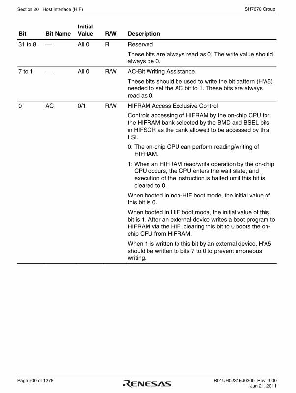
Section 20 Host Interface (HIF)
Page 900 of 1278 R01UH0234EJ0300 Rev. 3.00 Jun 21, 2011
SH7670 Group
Bit Bit Name Initial Value R/W Description
31 to 8 ⎯ All 0 R Reserved
These bits are always read as 0. The write value should always be 0.
7 to 1 ⎯ All 0 R/W AC-Bit Writing Assistance
These bits should be used to write the bit pattern (H'A5) needed to set the AC bit to 1. These bits are always read as 0.
0 AC 0/1 R/W HIFRAM Access Exclusive Control
Controls accessing of HIFRAM by the on-chip CPU for the HIFRAM bank selected by the BMD and BSEL bits in HIFSCR as the bank allowed to be accessed by this LSI.
0: The on-chip CPU can perform reading/writing of HIFRAM.
1: When an HIFRAM read/write operation by the on-chip CPU occurs, the CPU enters the wait state, and execution of the instruction is halted until this bit is cleared to 0.
When booted in non-HIF boot mode, the initial value of this bit is 0.
When booted in HIF boot mode, the initial value of this bit is 1. After an external device writes a boot program to HIFRAM via the HIF, clearing this bit to 0 boots the on-chip CPU from HIFRAM.
When 1 is written to this bit by an external device, H'A5 should be written to bits 7 to 0 to prevent erroneous writing.

Section 20 Host Interface (HIF)
R01UH0234EJ0300 Rev. 3.00 Page 901 of 1278 Jun 21, 2011
SH7670 Group
20.4.10 HIFDREQ Trigger Register (HIFDTR)
HIFDTR is a 32-bit register. Writing to HIFDTR by the on-chip CPU asserts the HIFDREQ pin. HIFDTR cannot be accessed by an external device.
31 30 29 28 27 26 25 24 23 22 21 20 19 18 17 16Bit:
Initial Value:R/W:
Bit:
Initial Value:R/W:
15 14 13 12 11 10 9 8 7 6 5 4 3 2 1 0
0 0 0 0 0 0 0 0 0 0 0 0 0 0 0 0R R R R R R R R R R R R R R R R
0 0 0 0 0 0 0 0 0 0 0 0 0 0 0 0R R R R R R R R R R R R R R R R/W
⎯ ⎯ ⎯ ⎯ ⎯ ⎯ ⎯ ⎯ ⎯
⎯
⎯ ⎯ ⎯ ⎯ ⎯
⎯ ⎯ ⎯ ⎯ - ⎯ ⎯ ⎯
⎯ ⎯
⎯ ⎯ ⎯ ⎯ ⎯ ⎯ ⎯ DTRG
Bit Bit Name Initial Value R/W Description
31 to 1 ⎯ All 0 R Reserved
These bits are always read as 0. The write value should always be 0.
0 DTRG 0 R/W HIFDREQ Trigger
When 1 is written to this bit, the HIFDREQ pin is asserted according to the setting of the DMD and DPOL bits in HIFSCR. This bit is automatically cleared to 0 in synchronization with negate of the HIFDREQ pin.
Though this bit can be set to 1 by the on-chip CPU, it cannot be cleared to 0.
To avoid conflict between clearing of this bit by negate of the HIFDREQ pin and setting of this bit by the on-chip CPU, make sure this bit is cleared to 0 before setting this bit to 1 by the on-chip CPU.
Writing 0 is invalid.
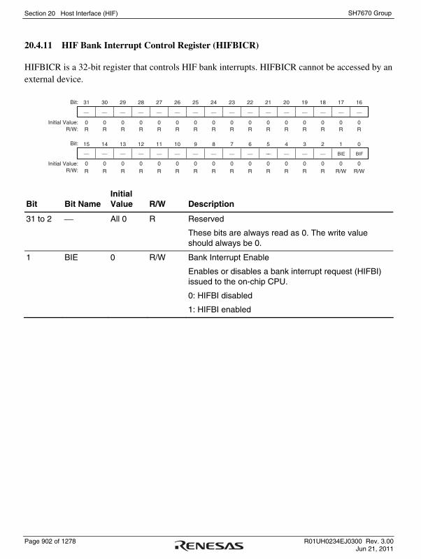
Section 20 Host Interface (HIF)
Page 902 of 1278 R01UH0234EJ0300 Rev. 3.00 Jun 21, 2011
SH7670 Group
20.4.11 HIF Bank Interrupt Control Register (HIFBICR)
HIFBICR is a 32-bit register that controls HIF bank interrupts. HIFBICR cannot be accessed by an external device.
R R R R R R R R R R R R R R R R
R R R R R R R R R R R R R R R/W R/W
31 30 29 28 27 26 25 24 23 22 21 20 19 18 17 16Bit:
Initial Value:R/W:
Bit:
Initial Value:R/W:
15 14 13 12 11 10 9 8 7 6 5 4 3 2 1 0
0 0 0 0 0 0 0 0 0 0 0 0 0 0 0 0
0 0 0 0 0 0 0 0 0 0 0 0 0 0 0 0
⎯ ⎯ ⎯ ⎯ ⎯ ⎯ ⎯ ⎯ ⎯
⎯
⎯ ⎯ ⎯ ⎯ ⎯
⎯ ⎯ ⎯ ⎯ - ⎯ ⎯ ⎯
⎯ ⎯
⎯ ⎯ ⎯ ⎯ ⎯ ⎯ BIE BIF
Bit Bit Name Initial Value R/W Description
31 to 2 ⎯ All 0 R Reserved
These bits are always read as 0. The write value should always be 0.
1 BIE 0 R/W Bank Interrupt Enable
Enables or disables a bank interrupt request (HIFBI) issued to the on-chip CPU.
0: HIFBI disabled
1: HIFBI enabled

Section 20 Host Interface (HIF)
R01UH0234EJ0300 Rev. 3.00 Page 903 of 1278 Jun 21, 2011
SH7670 Group
Bit Bit Name Initial Value R/W Description
0 BIF 0 R/W Bank Interrupt Request Flag
While this bit is 1, a bank interrupt request (HIFBI) is issued to the on-chip CPU according to the setting of the BIE bit.
In auto-increment mode (AI/AD bit in HIFMCR is 0), this bit is automatically set to 1 when an external device has completed access to the 32-bit data in the end address of HIFRAM and the HIFCS pin has been negated.
In auto-decrement mode (AI/AD bit in HIFMCR is 1), this bit is automatically set to 1 when an external device has completed access to the 32-bit data in the start address of HIFRAM and the HIFCS pin has been negated.
Though this bit can be cleared to 0 by the on-chip CPU, it cannot be set to 1.
Make sure setting of this bit by HIFRAM access from an external device and clearing of this bit by the on-chip CPU do not conflict using software.
Writing 1 is invalid.

Section 20 Host Interface (HIF)
Page 904 of 1278 R01UH0234EJ0300 Rev. 3.00 Jun 21, 2011
SH7670 Group
20.5 Memory Map
Table 20.3 shows the memory map of HIFRAM.
Table 20.3 Memory Map
Classification Start Address End Address Memory Size
Map from external device*1 H'0000 H'07FF 2 Kbytes
Map from on-chip CPU*1 *2 H'FFFF_F000 H'FFFF_F7FF 2 Kbytes
Notes: 1. Map for a single HIFRAM bank. Which bank is to be accessed by an external device or the on-chip CPU depends on the BMD and BSEL bits in HIFSCR. The mapping addresses are common between the banks.
2. In HIF boot mode, however, bank 0 is selected and the first 2 Kbytes of the first-half 32 Mbytes in the following areas are also mapped: (1) the cacheable area 0 in the H'0000_0000 to H'0000_07FF range and (2) the non-cacheable area 0 in the H'2000_0000 to H'2000_07FF range. If an external device modifies HIFRAM when HIFRAM is accessed from the cacheable area with the cache enabled, a coherency problem will occur. When the cache is enabled, accessing HIFRAM from the non-cacheable area is recommended. In HIF boot mode, among the first-half 32 Mbytes of each area 0, access to only the addresses to which HIFRAM is mapped is permitted. Even in HIF boot mode, the areas excluding the first-half 32 Mbytes of area 0 are mapped to the external memory as normally.

Section 20 Host Interface (HIF)
R01UH0234EJ0300 Rev. 3.00 Page 905 of 1278 Jun 21, 2011
SH7670 Group
20.6 Interface
20.6.1 Basic Sequence
Figure 20.3 shows the basic read/write sequence. HIF read is defined by the overlap period of the HIFRD low-level period and HIFCS low-level period, and HIF write is defined by the overlap period of the HIFWR low-level period and HIFCS low-level period. The HIFRS signal indicates whether this is normal access or index register access; low level indicates normal access and high level indicates index register access.
HIFCS
HIFRS
Write cycle Read cycle
HIFRD
HIFWR
HIFD15 to HIFD00 WT_D RD_D
Figure 20.3 Basic Timing for HIF Interface

Section 20 Host Interface (HIF)
Page 906 of 1278 R01UH0234EJ0300 Rev. 3.00 Jun 21, 2011
SH7670 Group
20.6.2 Reading/Writing of HIF Registers other than HIFIDX and HIFIDX
As shown in figure 20.4, in reading and writing of HIF internal registers other than HIFIDX and HIFIDX, first HIFRS is held high and HIFIDX is written to in order to select the register to be accessed and the byte location. Then HIFRS is held low, and reading or writing of the register selected by HIFIDX is performed.
HIFCS
HIFRS
HIFRD
HIFWR
HIFD15 to HIFD00 WT_DHIFIDX RD_D
Index write Register write Register read
Register selection
Figure 20.4 HIF Register Settings

Section 20 Host Interface (HIF)
R01UH0234EJ0300 Rev. 3.00 Page 907 of 1278 Jun 21, 2011
SH7670 Group
20.6.3 Consecutive Data Writing to HIFRAM by External Device
Figure 20.5 shows the timing chart for consecutive data transfer from an external device to HIFRAM. As shown in this timing chart, by setting the start address and the data to be written first, consecutive data transfer can subsequently be performed.
HIFCS
HIFRS
HIFRD
HIFWR
HIFD15 to HIFD00 0016 AHAL 0018 D0D1 001A D2D3 000A 00A0 0018 D4D5 D8D9D6D7
High level
HIFADR setting[15:8] = AH[7:0] = AL
Data for first write operationset in HIFDATA[31:24] = D0, [23:16] = D1,[15:8] = D2, [7:0] = D3
HIFMCR settingConsecutive writeAuto-increment
HIFDATAselection
Consecutive data writing
Figure 20.5 Consecutive Data Writing to HIFRAM

Section 20 Host Interface (HIF)
Page 908 of 1278 R01UH0234EJ0300 Rev. 3.00 Jun 21, 2011
SH7670 Group
20.6.4 Consecutive Data Reading from HIFRAM to External Device
Figure 20.6 shows the timing chart for consecutive data reading from HIFRAM to an external device. As this timing chart indicates, by setting the start address, data can subsequently be read out consecutively.
HIFCS
HIFRS
HIFRD
HIFWR
0016 AHAL 000A 0088 0018 D0D1 D2D3 D4D5 D6D7 D8D9 DCDDDADB
HIFADR setting[15:8] = AH[7:0] = AL
HIFMCR settingConsecutive readAuto-increment
Consecutive data readingHIFDATAselection
HIFD15 to HIFD00
Figure 20.6 Consecutive Data Reading from HIFRAM

Section 20 Host Interface (HIF)
R01UH0234EJ0300 Rev. 3.00 Page 909 of 1278 Jun 21, 2011
SH7670 Group
20.7 External DMAC Interface
Figures 20.7 to 20.10 show the HIFDREQ output timing. The start of the HIFDREQ assert synchronizes with the DTRG bit in HIFDTR being set to 1. The HIFDREQ negate timing and assert level are determined by the DMD and DPOL bits in HIFSCR, respectively.
When the external DMAC is specified to detect low level of the HIFDREQ signal, set DMD = 0 and DPOL = 0. After writing 1 to the DTRG bit, the HIFDREQ signal remains low until a read from or write to the HIFIDX-specified register is detected. Writing to the index register (HIFIDX) does not negate the signal.
DTRG bit
DPOL bit
HIFDREQ
Asserted in synchronization with the DTRG bit being set by the on-chip CPU.
The DTRG bit is cleared simultaneously with HIFDREQ negate.
Negated if a read from or write to the HIFIDX-specified register is detected.The latency is within tpcyc (cycle of the peripheral clock) × 5CYC.
HIFCS
HIFRS
Figure 20.7 HIFDREQ Timing (When DMD = 0 and DPOL = 0)
When the external DMAC is specified to detect high level of the HIFDREQ signal, set DMD = 0 and DPOL = 1. At the time the DPOL bit is set to 1, HIFDREQ becomes low. After this, the HIFDREQ signal remains low from when 1 is written to the DTRG bit until a read from or write to the HIFIDX-specified register is detected. Writing to the index register (HIFIDX) does not negate the signal.
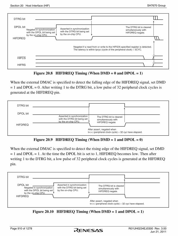
Section 20 Host Interface (HIF)
Page 910 of 1278 R01UH0234EJ0300 Rev. 3.00 Jun 21, 2011
SH7670 Group
DTRG bit
DPOL bit
HIFDREQ
HIFCS
HIFRS
Negated in synchronization with the DPOL bit being set by the on-chip CPU.
The DTRG bit is cleared simultaneously with HIFDREQ negate.
Negated if a read from or write to the HIFIDX-specified register is detected.The latency is within tpcyc (cycle of the peripheral clock) × 5CYC.
Asserted in synchronization with the DTRG bit being set by the on-chip CPU.
Figure 20.8 HIFDREQ Timing (When DMD = 0 and DPOL = 1)
When the external DMAC is specified to detect the falling edge of the HIFDREQ signal, set DMD = 1 and DPOL = 0. After writing 1 to the DTRG bit, a low pulse of 32 peripheral clock cycles is generated at the HIFDREQ pin.
DTRG bit
DPOL bit
HIFDREQ
After assert, negated when tPCYC (peripheral clock cycle) × 32 cyc have elapsed.
Asserted in synchronization with the DTRG bit being set by the on-chip CPU.
The DTRG bit is cleared simultaneously with HIFDREQ negate.
Figure 20.9 HIFDREQ Timing (When DMD = 1 and DPOL = 0)
When the external DMAC is specified to detect the rising edge of the HIFDREQ signal, set DMD = 1 and DPOL = 1. At the time the DPOL bit is set to 1, HIFDREQ becomes low. Then after writing 1 to the DTRG bit, a low pulse of 32 peripheral clock cycles is generated at the HIFDREQ pin.
DTRG bit
DPOL bit
HIFDREQ
After assert, negated when tPCYC (peripheral clock cycle) × 32 cyc have elapsed.
Asserted in synchronization with the DTRG bit being set by the on-chip CPU.
The DTRG bit is cleared simultaneously with HIFDREQ negate.
Negated in synchronization with the DPOL bit being set by the on-chip CPU.
Figure 20.10 HIFDREQ Timing (When DMD = 1 and DPOL = 1)
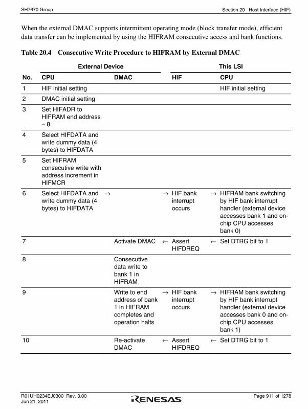
Section 20 Host Interface (HIF)
R01UH0234EJ0300 Rev. 3.00 Page 911 of 1278 Jun 21, 2011
SH7670 Group
When the external DMAC supports intermittent operating mode (block transfer mode), efficient data transfer can be implemented by using the HIFRAM consecutive access and bank functions.
Table 20.4 Consecutive Write Procedure to HIFRAM by External DMAC
External Device This LSI
No. CPU DMAC HIF CPU
1 HIF initial setting HIF initial setting
2 DMAC initial setting
3 Set HIFADR to HIFRAM end address − 8
4 Select HIFDATA and write dummy data (4 bytes) to HIFDATA
5 Set HIFRAM consecutive write with address increment in HIFMCR
6 Select HIFDATA and write dummy data (4 bytes) to HIFDATA
→ → HIF bank interrupt occurs
→ HIFRAM bank switching by HIF bank interrupt handler (external device accesses bank 1 and on-chip CPU accesses bank 0)
7 Activate DMAC ← Assert HIFDREQ
← Set DTRG bit to 1
8 Consecutive data write to bank 1 in HIFRAM
9 Write to end address of bank 1 in HIFRAM completes and operation halts
→ HIF bank interrupt occurs
→ HIFRAM bank switching by HIF bank interrupt handler (external device accesses bank 0 and on-chip CPU accesses bank 1)
10 Re-activate DMAC
← Assert HIFDREQ
← Set DTRG bit to 1
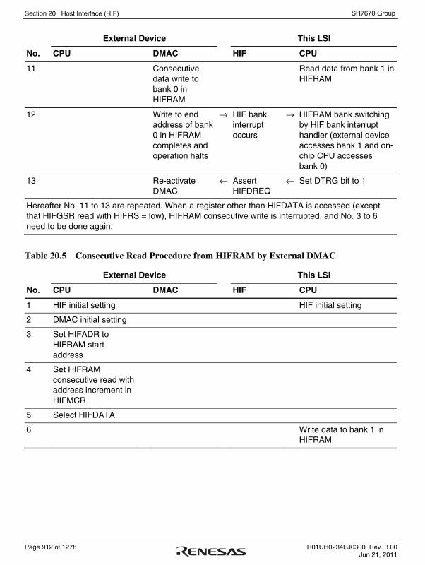
Section 20 Host Interface (HIF)
Page 912 of 1278 R01UH0234EJ0300 Rev. 3.00 Jun 21, 2011
SH7670 Group
External Device This LSI
No. CPU DMAC HIF CPU
11 Consecutive data write to bank 0 in HIFRAM
Read data from bank 1 in HIFRAM
12 Write to end address of bank 0 in HIFRAM completes and operation halts
→ HIF bank interrupt occurs
→ HIFRAM bank switching by HIF bank interrupt handler (external device accesses bank 1 and on-chip CPU accesses bank 0)
13 Re-activate DMAC
← Assert HIFDREQ
← Set DTRG bit to 1
Hereafter No. 11 to 13 are repeated. When a register other than HIFDATA is accessed (except that HIFGSR read with HIFRS = low), HIFRAM consecutive write is interrupted, and No. 3 to 6 need to be done again.
Table 20.5 Consecutive Read Procedure from HIFRAM by External DMAC
External Device This LSI
No. CPU DMAC HIF CPU
1 HIF initial setting HIF initial setting
2 DMAC initial setting
3 Set HIFADR to HIFRAM start address
4 Set HIFRAM consecutive read with address increment in HIFMCR
5 Select HIFDATA
6 Write data to bank 1 in HIFRAM

Section 20 Host Interface (HIF)
R01UH0234EJ0300 Rev. 3.00 Page 913 of 1278 Jun 21, 2011
SH7670 Group
External Device This LSI
No. CPU DMAC HIF CPU
7 After writing data to end address of bank 1 in HIFRAM, perform HIFRAM bank switching (external device accesses bank 1 and on-chip CPU accesses bank 0)
8 Activate DMAC ← Assert HIFDREQ
← Set DTRG bit to 1
9 Consecutive data read from bank 1 in HIFRAM
Write data to bank 0 in HIFRAM
10 Read from end address of bank 1 in HIFRAM completes and operation halts
→ HIF bank interrupt occurs
→ HIFRAM bank switching by HIF bank interrupt handler (external device accesses bank 0 and on-chip CPU accesses bank 1)
11 Re-activate DMAC
← Assert HIFDREQ
← Set DTRG bit to 1
12 Consecutive data read from bank 0 in HIFRAM
Write data to bank 1 in HIFRAM
13 Read from end address of bank 0 in HIFRAM completes and operation halts
→ HIF bank interrupt occurs
→ HIFRAM bank switching by HIF bank interrupt handler (external device accesses bank 1 and on-chip CPU accesses bank 0)
14 Re-activate DMAC
← Assert HIFDREQ
← Set DTRG bit to 1
Hereafter No. 12 to 14 are repeated. When a register other than HIFDATA is accessed (except that HIFGSR read with HIFRS = low), HIFRAM consecutive read is interrupted, and No. 3 to 5 need to be done again.

Section 20 Host Interface (HIF)
Page 914 of 1278 R01UH0234EJ0300 Rev. 3.00 Jun 21, 2011
SH7670 Group
20.8 Alignment Control
Tables 20.6 and 20.7 show the alignment control when an external device accesses the HIFDATA register, and the HIF registers other than the HIFDATA register, respectively.
Table 20.6 HIFDATA Register Alignment for Access by an External Device
Data in HIFDATA WBSWP Bit BO Bit BYTE[1:0] Bits Alignment in HIFD[15:0] Pins
0 0 B'00 H'7654
B'10 H'3210
1 B'00 H'3210
B'10 H'7654
1 0 B'00 H'1032
B'10 H'5476
1 B'00 H'5476
H'76543210
B'10 H'1032
Table 20.7 HIF Registers (other than HIFDATA) Alignment for Access by an External Device
Data in HIFDATA WBSWP Bit BO Bit BYTE[1:0] Bits Alignment in HIFD[15:0] Pins
0 B'00 H'7654
B'10 H'3210
1 B'00 H'3210
H'76543210 Don't care
B'10 H'7654
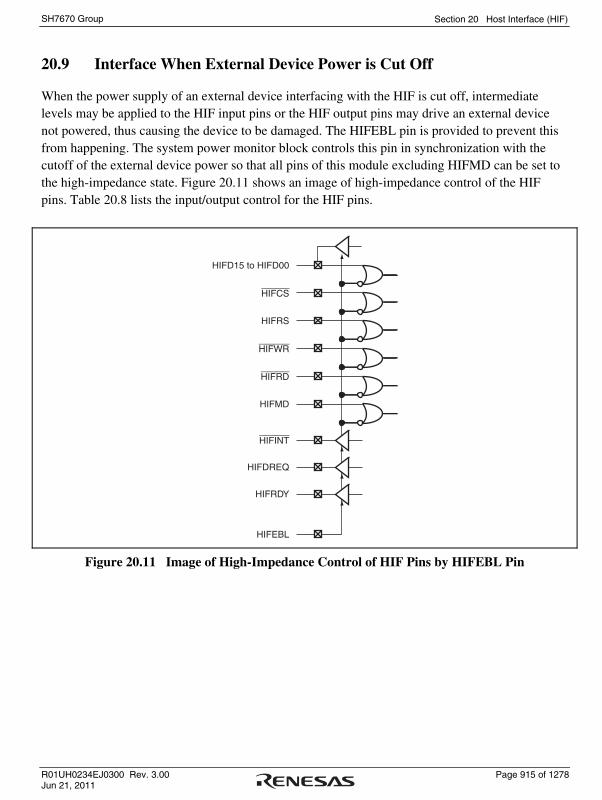
Section 20 Host Interface (HIF)
R01UH0234EJ0300 Rev. 3.00 Page 915 of 1278 Jun 21, 2011
SH7670 Group
20.9 Interface When External Device Power is Cut Off
When the power supply of an external device interfacing with the HIF is cut off, intermediate levels may be applied to the HIF input pins or the HIF output pins may drive an external device not powered, thus causing the device to be damaged. The HIFEBL pin is provided to prevent this from happening. The system power monitor block controls this pin in synchronization with the cutoff of the external device power so that all pins of this module excluding HIFMD can be set to the high-impedance state. Figure 20.11 shows an image of high-impedance control of the HIF pins. Table 20.8 lists the input/output control for the HIF pins.
HIFCS
HIFWR
HIFRD
HIFD15 to HIFD00
HIFRS
HIFMD
HIFINT
HIFDREQ
HIFRDY
HIFEBL
Figure 20.11 Image of High-Impedance Control of HIF Pins by HIFEBL Pin

Section 20 Host Interface (HIF)
Page 916 of 1278 R01UH0234EJ0300 Rev. 3.00 Jun 21, 2011
SH7670 Group
Table 20.8 Input/Output Control for HIF Pins
LSI Status Reset State by RES Pin Reset Canceled by RES Pin
HIFMD input level
High (Boot setting)
Low (Non-boot setting)
The reset by the RES pin is
released while the HIFMD
signal is high.
(boot mode established)
The reset by the RES pin is
released while the HIFMD
signal is low
(non-boot mode established)
HIFEBL input level Low High
The HIFEBL pin is a
general input port
and the HIF is not
controlled by the
signal input on this
pin. Low High General input port at the initial state *1
HIFRDY output control
Output buffer: On (Low output)
Output buffer: On (Low output)
General input port Output buffer: Off
Output buffer: On (Sequence output)
General input port at the initial state*2
HIFINT output control
Output buffer: Off
Output buffer: Off
General input port Output buffer: Off
Output buffer: On (Sequence output)
General input port at the initial state*2
HIFDREQ output control
Output buffer: Off
Output buffer: Off
General input port Output buffer: Off
Output buffer: On (Sequence output)
General input port at the initial state*2
HIFD 15 to HIFD0 I/O control
I/O buffer: Off
I/O buffer: Off
General input port I/O buffer: Off
I/O buffer controlled according to states of HIFCS, HIFWR, and HIFRD
General input port at the initial state*2
HIFCS input control
Input buffer: Off
Input buffer: Off
General input port Input buffer: Off
Input buffer: On
General input port at the initial state*2
HIFRS input control
Input buffer: Off
Input buffer: Off
General input port Input buffer: Off
Input buffer: On
General input port at the initial state*2

Section 20 Host Interface (HIF)
R01UH0234EJ0300 Rev. 3.00 Page 917 of 1278 Jun 21, 2011
SH7670 Group
LSI Status Reset State by RES Pin Reset Canceled by RES Pin
HIFMD input level
High (Boot setting)
Low (Non-boot setting)
High (After the reset canceled by boot setting)
Low (After the reset canceled by non-boot setting)
HIFEBL input level Low High
The HIFEBL pin is a general input port and the HIF is not controlled by the signal input on this pin. Low High
General input port at the initial state *1
HIFWR input control
Input buffer: Off
Input buffer: Off
General input port Input buffer: Off
Input buffer: On
General input port at the initial state*2
HIFRD input control
Input buffer: Off
Input buffer: Off General input port
Input buffer: Off
Input buffer: On
General input port at the initial state*2
Notes: 1. The pin also functions as an HIFEBL pin by setting the PFC registers.
2. The pin also functions as an HIF pin by setting the PFC registers.
When the HIF pin function is selected for the HIFEBL pin and this pin by setting the PFC registers, the input and/or output buffers are controlled according to the HIFEBL pin state.
When the HIF pin function is not selected for the HIFEBL pin and is selected for this pin by setting the PFC registers, the input and/or output buffers are always turned off. This setting is prohibited.

Section 20 Host Interface (HIF)
Page 918 of 1278 R01UH0234EJ0300 Rev. 3.00 Jun 21, 2011
SH7670 Group
20.10 Usage Notes
(1) Conflict between Access from External Device and Access from Internal Bus (from CPU or DMAC of This LSI) to HIF Registers
Regarding HIF related registers which can be accessed from both an external device and the internal bus, take measures to avoid a conflict between a read/write operation from an external device and a write operation from the internal bus.
When a read operation from an external device conflicts with a write operation from the internal bus, the read data at the HIFD[15:0] pins will be updated in the middle of a read cycle by the external device. When a write operation from an external device conflicts with a write operation from the internal bus, the write operation from the internal bus is ignored. In this case, the CPU or DMAC of this LSI is not notified of an error.
A conflict between a read/write operation from an external device and a read operation from the internal bus will not cause any problem.
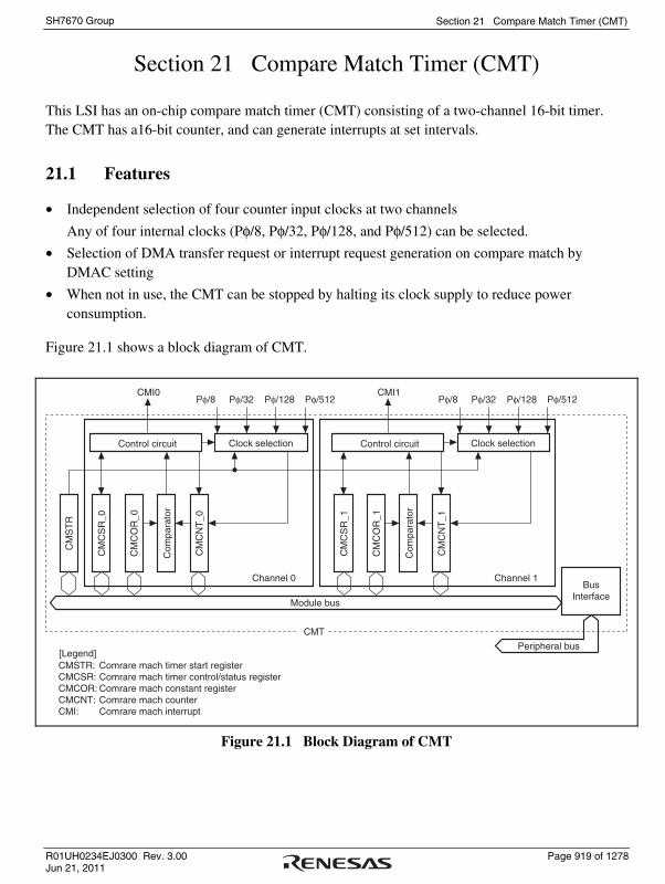
Section 21 Compare Match Timer (CMT)
R01UH0234EJ0300 Rev. 3.00 Page 919 of 1278 Jun 21, 2011
SH7670 Group
Section 21 Compare Match Timer (CMT)
This LSI has an on-chip compare match timer (CMT) consisting of a two-channel 16-bit timer. The CMT has a16-bit counter, and can generate interrupts at set intervals.
21.1 Features
• Independent selection of four counter input clocks at two channels
Any of four internal clocks (Pφ/8, Pφ/32, Pφ/128, and Pφ/512) can be selected.
• Selection of DMA transfer request or interrupt request generation on compare match by DMAC setting
• When not in use, the CMT can be stopped by halting its clock supply to reduce power consumption.
Figure 21.1 shows a block diagram of CMT.
Peripheral bus
BusInterface
Control circuit Clock selection
CM
ST
R
CM
CS
R_0
CM
CO
R_0
Com
para
tor
CM
CN
T_0
Module bus
Channel 0 Channel 1
CMT
CMI0Pφ/8 Pφ/32 Pφ/128 Pφ/512
CMI1
CMSTR:CMCSR:CMCOR:CMCNT:CMI:
Comrare mach timer start registerComrare mach timer control/status registerComrare mach constant registerComrare mach counterComrare mach interrupt
Control circuit Clock selection
CM
CS
R_1
CM
CO
R_1
Com
para
tor
CM
CN
T_1
Pφ/8 Pφ/32 Pφ/128 Pφ/512
[Legend]
Figure 21.1 Block Diagram of CMT
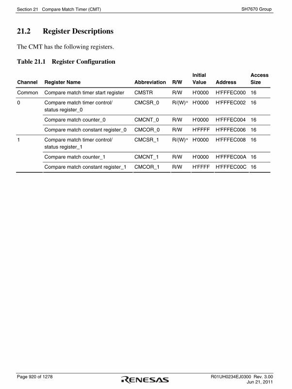
Section 21 Compare Match Timer (CMT)
Page 920 of 1278 R01UH0234EJ0300 Rev. 3.00 Jun 21, 2011
SH7670 Group
21.2 Register Descriptions
The CMT has the following registers.
Table 21.1 Register Configuration
Channel Register Name Abbreviation R/W Initial Value Address
Access Size
Common Compare match timer start register CMSTR R/W H'0000 H'FFFEC000 16
Compare match timer control/ status register_0
CMCSR_0 R/(W)* H'0000 H'FFFEC002 16
Compare match counter_0 CMCNT_0 R/W H'0000 H'FFFEC004 16
0
Compare match constant register_0 CMCOR_0 R/W H'FFFF H'FFFEC006 16
Compare match timer control/ status register_1
CMCSR_1 R/(W)* H'0000 H'FFFEC008 16
Compare match counter_1 CMCNT_1 R/W H'0000 H'FFFEC00A 16
1
Compare match constant register_1 CMCOR_1 R/W H'FFFF H'FFFEC00C 16

Section 21 Compare Match Timer (CMT)
R01UH0234EJ0300 Rev. 3.00 Page 921 of 1278 Jun 21, 2011
SH7670 Group
21.2.1 Compare Match Timer Start Register (CMSTR)
CMSTR is a 16-bit register that selects whether compare match counter (CMCNT) operates or is stopped.
CMSTR is initialized to H'0000 by a power-on reset or in software standby mode, but retains its previous value in module standby mode.
Bit:
Initial value:R/W:
15 14 13 12 11 10 9 8 7 6 5 4 3 2 1 0
0 0 0 0 0 0 0 0 0 0 0 0 0 0 0 0R R R R R R R R R R R R R R R/W R/W
- - - - - - -- - - - - - - STR1 STR0
Bit Bit Name Initial Value R/W Description
15 to 2 ⎯ All 0 R Reserved
These bits are always read as 0. The write value should always be 0.
1 STR1 0 R/W Count Start 1
Specifies whether compare match counter_1 operates or is stopped.
0: CMCNT_1 count is stopped
1: CMCNT_1 count is started
0 STR0 0 R/W Count Start 0
Specifies whether compare match counter_0 operates or is stopped.
0: CMCNT_0 count is stopped
1: CMCNT_0 count is started

Section 21 Compare Match Timer (CMT)
Page 922 of 1278 R01UH0234EJ0300 Rev. 3.00 Jun 21, 2011
SH7670 Group
21.2.2 Compare Match Timer Control/Status Register (CMCSR)
CMCSR is a 16-bit register that indicates compare match generation, enables or disables interrupts, and selects the counter input clock.
CMCSR is initialized to H'0000 by a power-on reset or in software standby mode, but retains its previous value in module standby mode.
15 14 13 12 11 10 9 8 7 6 5 4 3 2 1 0
0 0 0 0 0 0 0 0 0 0 0 0 0 0 0 0R R R R R R R R R/(W)* R/W R R R R R/W R/W
Bit:
Initial value:R/W:
Note: Only 0 can be written to clear the flag after 1 is read.*
- - - - - - - - CMF CMIE - - - - CKS[1:0]
Bit Bit Name Initial Value R/W Description
15 to 8 ⎯ All 0 R Reserved
These bits are always read as 0. The write value should always be 0.
7 CMF 0 R/(W)* Compare Match Flag
Indicates whether or not the values of CMCNT and CMCOR match.
0: CMCNT and CMCOR values do not match
[Clearing condition]
• When 0 is written to CMF after reading CMF = 1
1: CMCNT and CMCOR values match
6 CMIE 0 R/W Compare Match Interrupt Enable
Enables or disables compare match interrupt (CMI) generation when CMCNT and CMCOR values match (CMF = 1).
0: Compare match interrupt (CMI) disabled
1: Compare match interrupt (CMI) enabled
5 to 2 ⎯ All 0 R Reserved
These bits are always read as 0. The write value should always be 0.

Section 21 Compare Match Timer (CMT)
R01UH0234EJ0300 Rev. 3.00 Page 923 of 1278 Jun 21, 2011
SH7670 Group
Bit Bit Name Initial Value R/W Description
1, 0 CKS[1:0] 00 R/W Clock Select
These bits select the clock to be input to CMCNT from four internal clocks obtained by dividing the peripheral clock (Pφ). When the STR bit in CMSTR is set to 1, CMCNT starts counting on the clock selected with bits CKS[1:0].
00: Pφ/8
01: Pφ/32
10: Pφ/128
11: Pφ/512
Note: * Only 0 can be written to clear the flag after 1 is read.
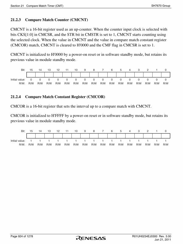
Section 21 Compare Match Timer (CMT)
Page 924 of 1278 R01UH0234EJ0300 Rev. 3.00 Jun 21, 2011
SH7670 Group
21.2.3 Compare Match Counter (CMCNT)
CMCNT is a 16-bit register used as an up-counter. When the counter input clock is selected with bits CKS[1:0] in CMCSR, and the STR bit in CMSTR is set to 1, CMCNT starts counting using the selected clock. When the value in CMCNT and the value in compare match constant register (CMCOR) match, CMCNT is cleared to H'0000 and the CMF flag in CMCSR is set to 1.
CMCNT is initialized to H'0000 by a power-on reset or in software standby mode, but retains its previous value in module standby mode.
15 14 13 12 11 10 9 8 7 6 5 4 3 2 1 0
0 0 0 0 0 0 0 0 0 0 0 0 0 0 0 0R/W R/W R/W R/W R/W R/W R/W R/W R/W R/W R/W R/W R/W R/W R/W R/W
Bit:
Initial value:R/W:
21.2.4 Compare Match Constant Register (CMCOR)
CMCOR is a 16-bit register that sets the interval up to a compare match with CMCNT.
CMCOR is initialized to H'FFFF by a power-on reset or in software standby mode, but retains its previous value in module standby mode.
15 14 13 12 11 10 9 8 7 6 5 4 3 2 1 0
1 1 1 1 1 1 1 1 1 1 1 1 1 1 1 1R/W R/W R/W R/W R/W R/W R/W R/W R/W R/W R/W R/W R/W R/W R/W R/W
Bit:
Initial value:R/W:

Section 21 Compare Match Timer (CMT)
R01UH0234EJ0300 Rev. 3.00 Page 925 of 1278 Jun 21, 2011
SH7670 Group
21.3 Operation
21.3.1 Interval Count Operation
When an internal clock is selected with the CKS[1:0] bits in CMCSR and the STR bit in CMSTR is set to 1, CMCNT starts incrementing using the selected clock. When the values in CMCNT and CMCOR match, CMCNT is cleared to H'0000 and the CMF flag in CMCSR is set to 1. When the CMIE bit in CMCSR is set to 1 at this time, a compare match interrupt (CMI) is requested. CMCNT then starts counting up again from H'0000.
Figure 21.2 shows the operation of the compare match counter.
CMCOR
H'0000
CMCNT value
Time
Counter cleared by compare match with CMCOR
Figure 21.2 Counter Operation
21.3.2 CMCNT Count Timing
One of four clocks (Pφ/8, Pφ/32, Pφ/128, and Pφ/512) obtained by dividing the peripheral clock (Pφ) can be selected with the CKS[1:0] bits in CMCSR. Figure 21.3 shows the timing.
CMCNT N N + 1
Peripheral clock (Pφ)
ClockN
ClockN + 1
Internal clock
Count clock
Figure 21.3 Count Timing

Section 21 Compare Match Timer (CMT)
Page 926 of 1278 R01UH0234EJ0300 Rev. 3.00 Jun 21, 2011
SH7670 Group
21.4 Interrupts
21.4.1 Interrupt Sources and DMA Transfer Requests
The CMT has channels and each of them to which a different vector address is allocated has a compare match interrupt. When both the compare match flag (CMF) and the interrupt enable bit (CMIE) are set to 1, the corresponding interrupt request is output. When the interrupt is used to activate a CPU interrupt, the priority of channels can be changed by the interrupt controller settings. For details, see section 6, Interrupt Controller (INTC).
Clear the CMF bit to 0 by the user exception handling routine. If this operation is not carried out, another interrupt will be generated. The direct memory access controller (DMAC) can be set to be activated when a compare match interrupt is requested. In this case, an interrupt is not issued to the CPU. If the setting to activate the DMAC has not been made, an interrupt request is sent to the CPU. The CMF bit is automatically cleared to 0 when data is transferred by the DMAC.
21.4.2 Timing of Compare Match Flag Setting
When CMCOR and CMCNT match, a compare match signal is generated at the last state in which the values match (the timing when the CMCNT value is updated to H'0000) and the CMF bit in CMCSR is set to 1. That is, after a match between CMCOR and CMCNT, the compare match signal is not generated until the next CMCNT counter clock input. Figure 21.4 shows the timing of CMF bit setting.
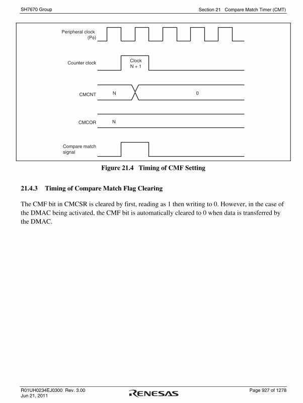
Section 21 Compare Match Timer (CMT)
R01UH0234EJ0300 Rev. 3.00 Page 927 of 1278 Jun 21, 2011
SH7670 Group
CMCNT
CMCOR
N
N
0
Peripheral clock (Pφ)
Counter clock
Compare matchsignal
ClockN + 1
Figure 21.4 Timing of CMF Setting
21.4.3 Timing of Compare Match Flag Clearing
The CMF bit in CMCSR is cleared by first, reading as 1 then writing to 0. However, in the case of the DMAC being activated, the CMF bit is automatically cleared to 0 when data is transferred by the DMAC.

Section 21 Compare Match Timer (CMT)
Page 928 of 1278 R01UH0234EJ0300 Rev. 3.00 Jun 21, 2011
SH7670 Group
21.5 Usage Notes
21.5.1 Conflict between Write and Compare-Match Processes of CMCNT
When the compare match signal is generated in the T2 cycle while writing to CMCNT, clearing CMCNT has priority over writing to it. In this case, CMCNT is not written to. Figure 21.5 shows the timing to clear the CMCNT counter.
CMCNT
T1 T2
CMCNT
H'0000N
Peripheral clock (Pφ)
Address signal
Internal write signal
Counter clear signal
CMCSR write cycle
Figure 21.5 Conflict between Write and Compare Match Processes of CMCNT

Section 21 Compare Match Timer (CMT)
R01UH0234EJ0300 Rev. 3.00 Page 929 of 1278 Jun 21, 2011
SH7670 Group
21.5.2 Conflict between Word-Write and Count-Up Processes of CMCNT
Even when the count-up occurs in the T2 cycle while writing to CMCNT in words, the writing has priority over the count-up. In this case, the count-up is not performed. Figure 21.6 shows the timing to write to CMCNT in words.
CMCNT
T1 T2
CMCNT
MN
Peripheral clock (Pφ)
Address signal
Internal write signal
CMCNT count-upenable signal
CMCSR write cycle
Figure 21.6 Conflict between Word-Write and Count-Up Processes of CMCNT
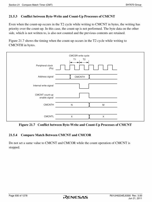
Section 21 Compare Match Timer (CMT)
Page 930 of 1278 R01UH0234EJ0300 Rev. 3.00 Jun 21, 2011
SH7670 Group
21.5.3 Conflict between Byte-Write and Count-Up Processes of CMCNT
Even when the count-up occurs in the T2 cycle while writing to CMCNT in bytes, the writing has priority over the count-up. In this case, the count-up is not performed. The byte data on the other side, which is not written to, is also not counted and the previous contents are retained.
Figure 21.7 shows the timing when the count-up occurs in the T2 cycle while writing to CMCNTH in bytes.
CMCNTH
T1 T2
CMCNTH
MN
CMCNTL XX
Peripheral clock (Pφ)
Address signal
Internal write signal
CMCNT count-upenable signal
CMCSR write cycle
Figure 21.7 Conflict between Byte-Write and Count-Up Processes of CMCNT
21.5.4 Compare Match Between CMCNT and CMCOR
Do not set a same value to CMCNT and CMCOR while the count operation of CMCNT is stopped.

Section 22 Serial Communication Interface with FIFO (SCIF)
R01UH0234EJ0300 Rev. 3.00 Page 931 of 1278 Jun 21, 2011
SH7670 Group
Section 22 Serial Communication Interface with FIFO (SCIF)
This LSI has a three-channel serial communication interface with FIFO (SCIF) that supports both asynchronous and clocked synchronous serial communication. It also has 16-stage FIFO registers for both transmission and reception independently for each channel that enable this LSI to perform efficient high-speed continuous communication.
22.1 Features
• Asynchronous serial communication:
⎯ Serial data communication is performed by start-stop in character units. The SCIF can communicate with a universal asynchronous receiver/transmitter (UART), an asynchronous communication interface adapter (ACIA), or any other communications chip that employs a standard asynchronous serial system. There are eight selectable serial data communication formats.
⎯ Data length: 7 or 8 bits
⎯ Stop bit length: 1 or 2 bits
⎯ Parity: Even, odd, or none
⎯ Receive error detection: Parity, framing, and overrun errors
⎯ Break detection: Break is detected when a framing error is followed by at least one frame at the space 0 level (low level). It is also detected by reading the RxD level directly from the serial port register when a framing error occurs.
• Clocked synchronous serial communication:
⎯ Serial data communication is synchronized with a clock signal. The SCIF can communicate with other chips having a clocked synchronous communication function. There is one serial data communication format.
⎯ Data length: 8 bits
⎯ Receive error detection: Overrun errors
• Full duplex communication: The transmitting and receiving sections are independent, so the SCIF can transmit and receive simultaneously. Both sections use 16-stage FIFO buffering, so high-speed continuous data transfer is possible in both the transmit and receive directions.
• On-chip baud rate generator with selectable bit rates
• Internal or external transmit/receive clock source: From either baud rate generator (internal) or SCK pin (external)

Section 22 Serial Communication Interface with FIFO (SCIF)
Page 932 of 1278 R01UH0234EJ0300 Rev. 3.00 Jun 21, 2011
SH7670 Group
• Four types of interrupts: Transmit-FIFO-data-empty interrupt, break interrupt, receive-FIFO-data-full interrupt, and receive-error interrupts are requested independently.
• When the SCIF is not in use, it can be stopped by halting the clock supplied to it, saving power.
• In asynchronous mode, on-chip modem control functions (RTS and CTS).
• The quantity of data in the transmit and receive FIFO data registers and the number of receive errors of the receive data in the receive FIFO data register can be ascertained.
• A time-out error (DR) can be detected when receiving in asynchronous mode. Figure 22.1 shows a block diagram of the SCIF.
Pφ
SCFRDR (16 stage) SCFTDR (16 stage)
SCRSR SCTSR
SCSMR
SCLSR
SCFDR
SCFCR
SCFSR
SCSCR
SCSPTR
SCBRR
TXIRXIERIBRI
Pφ/4
Pφ/16
Pφ/64
RTS
CTS
SCK
TxD
RxD
SCIF
Module data bus
Parity generation
Parity check
Transmission/receptioncontrol
Baud rategenerator
Clock
External clockB
us in
terf
ace
Peripheralbus
SCRSR:SCFRDR:SCTSR:SCFTDR:SCSMR:SCSCR:
[Legend]SCFSR:SCBRR:SCSPTR:SCFCR:SCFDR:SCLSR:
Receive shift registerReceive FIFO data registerTransmit shift registerTransmit FIFO data registerSerial mode registerSerial control register
Serial status registerBit rate registerSerial port registerFIFO control registerFIFO data count set registerLine status register
Figure 22.1 Block Diagram of SCIF

Section 22 Serial Communication Interface with FIFO (SCIF)
R01UH0234EJ0300 Rev. 3.00 Page 933 of 1278 Jun 21, 2011
SH7670 Group
22.2 Input/Output Pins
Table 22.1 shows the pin configuration of the SCIF.
Table 22.1 Pin Configuration
Channel Pin Name Symbol I/O Function
Serial clock pins SCK0 to SCK2 I/O Clock I/O
Receive data pins RxD0 to RxD2 Input Receive data input
Transmit data pins TxD0 to TxD2 Output Transmit data output
Request to send pin RTS0 to RTS2 I/O Request to send
0 to 2
Clear to send pin CTS0 to CTS2 I/O Clear to send
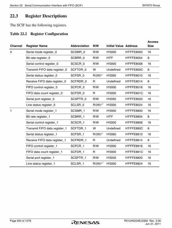
Section 22 Serial Communication Interface with FIFO (SCIF)
Page 934 of 1278 R01UH0234EJ0300 Rev. 3.00 Jun 21, 2011
SH7670 Group
22.3 Register Descriptions
The SCIF has the following registers.
Table 22.2 Register Configuration
Channel Register Name Abbreviation R/W Initial Value Address Access Size
Serial mode register_0 SCSMR_0 R/W H'0000 H'FFFE8000 16
Bit rate register_0 SCBRR_0 R/W H'FF H'FFFE8004 8
Serial control register_0 SCSCR_0 R/W H'0000 H'FFFE8008 16
Transmit FIFO data register_0 SCFTDR_0 W Undefined H'FFFE800C 8
Serial status register_0 SCFSR_0 R/(W)*1 H'0060 H'FFFE8010 16
Receive FIFO data register_0 SCFRDR_0 R Undefined H'FFFE8014 8
FIFO control register_0 SCFCR_0 R/W H'0000 H'FFFE8018 16
FIFO data count register_0 SCFDR_0 R H'0000 H'FFFE801C 16
Serial port register_0 SCSPTR_0 R/W H'0050 H'FFFE8020 16
0
Line status register_0 SCLSR_0 R/(W)*2 H'0000 H'FFFE8024 16
Serial mode register_1 SCSMR_1 R/W H'0000 H'FFFE8800 16
Bit rate register_1 SCBRR_1 R/W H'FF H'FFFE8804 8
Serial control register_1 SCSCR_1 R/W H'0000 H'FFFE8808 16
Transmit FIFO data register_1 SCFTDR_1 W Undefined H'FFFE880C 8
Serial status register_1 SCFSR_1 R/(W)*1 H'0060 H'FFFE8810 16
Receive FIFO data register_1 SCFRDR_1 R Undefined H'FFFE8814 8
FIFO control register_1 SCFCR_1 R/W H'0000 H'FFFE8818 16
FIFO data count register_1 SCFDR_1 R H'0000 H'FFFE881C 16
Serial port register_1 SCSPTR_1 R/W H'0050 H'FFFE8820 16
1
Line status register_1 SCLSR_1 R/(W)*2 H'0000 H'FFFE8824 16

Section 22 Serial Communication Interface with FIFO (SCIF)
R01UH0234EJ0300 Rev. 3.00 Page 935 of 1278 Jun 21, 2011
SH7670 Group
Channel Register Name Abbreviation R/W Initial Value Address Access Size
Serial mode register_2 SCSMR_2 R/W H'0000 H'FFFE9000 16
Bit rate register_2 SCBRR_2 R/W H'FF H'FFFE9004 8
Serial control register_2 SCSCR_2 R/W H'0000 H'FFFE9008 16
Transmit FIFO data register_2 SCFTDR_2 W Undefined H'FFFE900C 8
Serial status register_2 SCFSR_2 R/(W)*1 H'0060 H'FFFE9010 16
Receive FIFO data register_2 SCFRDR_2 R Undefined H'FFFE9014 8
FIFO control register_2 SCFCR_2 R/W H'0000 H'FFFE9018 16
FIFO data count register_2 SCFDR_2 R H'0000 H'FFFE901C 16
Serial port register_2 SCSPTR_2 R/W H'0050 H'FFFE9020 16
2
Line status register_2 SCLSR_2 R/(W)*2 H'0000 H'FFFE9024 16
Notes: 1. Only 0 can be written to clear the flag. Bits 15 to 8, 3, and 2 are read-only bits that cannot be modified.
2. Only 0 can be written to clear the flag. Bits 15 to 1 are read-only bits that cannot be modified.
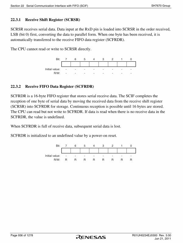
Section 22 Serial Communication Interface with FIFO (SCIF)
Page 936 of 1278 R01UH0234EJ0300 Rev. 3.00 Jun 21, 2011
SH7670 Group
22.3.1 Receive Shift Register (SCRSR)
SCRSR receives serial data. Data input at the RxD pin is loaded into SCRSR in the order received, LSB (bit 0) first, converting the data to parallel form. When one byte has been received, it is automatically transferred to the receive FIFO data register (SCFRDR).
The CPU cannot read or write to SCRSR directly.
7 6 5 4 3 2 1 0
- - - - - - - -- - - - - - - -
Bit:
Initial value:R/W:
22.3.2 Receive FIFO Data Register (SCFRDR)
SCFRDR is a 16-byte FIFO register that stores serial receive data. The SCIF completes the reception of one byte of serial data by moving the received data from the receive shift register (SCRSR) into SCFRDR for storage. Continuous reception is possible until 16 bytes are stored. The CPU can read but not write to SCFRDR. If data is read when there is no receive data in the SCFRDR, the value is undefined.
When SCFRDR is full of receive data, subsequent serial data is lost.
SCFRDR is initialized to an undefined value by a power-on reset.
7 6 5 4 3 2 1 0
- - - - - - - -R R R R R R R R
Bit:
Initial value:R/W:

Section 22 Serial Communication Interface with FIFO (SCIF)
R01UH0234EJ0300 Rev. 3.00 Page 937 of 1278 Jun 21, 2011
SH7670 Group
22.3.3 Transmit Shift Register (SCTSR)
SCTSR transmits serial data. The SCIF loads transmit data from the transmit FIFO data register (SCFTDR) into SCTSR, then transmits the data serially from the TxD pin, LSB (bit 0) first. After transmitting one data byte, the SCIF automatically loads the next transmit data from SCFTDR into SCTSR and starts transmitting again.
The CPU cannot read or write to SCTSR directly.
7 6 5 4 3 2 1 0
- - - - - - - -- - - - - - - -
Bit:
Initial value:R/W:
22.3.4 Transmit FIFO Data Register (SCFTDR)
SCFTDR is a 16-byte FIFO register that stores data for serial transmission. When the SCIF detects that the transmit shift register (SCTSR) is empty, it moves transmit data written in the SCFTDR into SCTSR and starts serial transmission. Continuous serial transmission is performed until there is no transmit data left in SCFTDR. The CPU can write to SCFTDR at all times.
When SCFTDR is full of transmit data (16 bytes), no more data can be written. If writing of new data is attempted, the data is ignored.
SCFTDR is initialized to an undefined value by a power-on reset.
7 6 5 4 3 2 1 0
- - - - - - - -W W W W W W W W
Bit:
Initial value:R/W:

Section 22 Serial Communication Interface with FIFO (SCIF)
Page 938 of 1278 R01UH0234EJ0300 Rev. 3.00 Jun 21, 2011
SH7670 Group
22.3.5 Serial Mode Register (SCSMR)
SCSMR specifies the SCIF serial communication format and selects the clock source for the baud rate generator.
The CPU can always read and write to SCSMR. SCSMR is initialized to H'0000 by a power-on reset.
15 14 13 12 11 10 9 8 7 6 5 4 3 2 1 0
0 0 0 0 0 0 0 0 0 0 0 0 0 0 0 0R R R R R R R R R/W R/W R/W R/W R/W R R/W R/W
Bit:
Initial value:R/W:
- - - - - - - - C/A CHR PE O/E STOP - CKS[1:0]
Bit Bit Name Initial Value R/W Description
15 to 8 ⎯ All 0 R Reserved
These bits are always read as 0. The write value should always be 0.
7 C/A 0 R/W Communication Mode
Selects whether the SCIF operates in asynchronous or clocked synchronous mode.
0: Asynchronous mode
1: Clocked synchronous mode
6 CHR 0 R/W Character Length
Selects 7-bit or 8-bit data length in asynchronous mode. In the clocked synchronous mode, the data length is always 8 bits, regardless of the CHR setting.
0: 8-bit data
1: 7-bit data*
Note: * When 7-bit data is selected, the MSB (bit 7) of the transmit FIFO data register is not transmitted.

Section 22 Serial Communication Interface with FIFO (SCIF)
R01UH0234EJ0300 Rev. 3.00 Page 939 of 1278 Jun 21, 2011
SH7670 Group
Bit Bit Name Initial Value R/W Description
5 PE 0 R/W Parity Enable
Selects whether to add a parity bit to transmit data and to check the parity of receive data, in asynchronous mode. In clocked synchronous mode, a parity bit is neither added nor checked, regardless of the PE setting.
0: Parity bit not added or checked
1: Parity bit added and checked*
Note: * When PE is set to 1, an even or odd parity bit is added to transmit data, depending on the parity mode (O/E) setting. Receive data parity is checked according to the even/odd (O/E) mode setting.
4 O/E 0 R/W Parity mode
Selects even or odd parity when parity bits are added and checked. The O/E setting is used only in asynchronous mode and only when the parity enable bit (PE) is set to 1 to enable parity addition and checking. The O/E setting is ignored in clocked synchronous mode, or in asynchronous mode when parity addition and checking is disabled.
0: Even parity*1
1: Odd parity*2
Notes: 1. If even parity is selected, the parity bit is added to transmit data to make an even number of 1s in the transmitted character and parity bit combined. Receive data is checked to see if it has an even number of 1s in the received character and parity bit combined.
2. If odd parity is selected, the parity bit is added to transmit data to make an odd number of 1s in the transmitted character and parity bit combined. Receive data is checked to see if it has an odd number of 1s in the received character and parity bit combined.

Section 22 Serial Communication Interface with FIFO (SCIF)
Page 940 of 1278 R01UH0234EJ0300 Rev. 3.00 Jun 21, 2011
SH7670 Group
Bit Bit Name Initial Value R/W Description
3 STOP 0 R/W Stop Bit Length
Selects one or two bits as the stop bit length in asynchronous mode. This setting is used only in asynchronous mode. It is ignored in clocked synchronous mode because no stop bits are added.
When receiving, only the first stop bit is checked, regardless of the STOP bit setting. If the second stop bit is 1, it is treated as a stop bit, but if the second stop bit is 0, it is treated as the start bit of the next incoming character.
0: One stop bit When transmitting, a single 1-bit is added at the end of each transmitted character.
1: Two stop bits When transmitting, two 1 bits are added at the end of each transmitted character.
2 ⎯ 0 R Reserved
This bit is always read as 0. The write value should always be 0.
1, 0 CKS[1:0] 00 R/W Clock Select
Select the internal clock source of the on-chip baud rate generator. For further information on the clock source, bit rate register settings, and baud rate, see section 22.3.8, Bit Rate Register (SCBRR).
00: Pφ
01: Pφ/4
10: Pφ/16
11: Pφ/64
Note: Pφ: Peripheral clock

Section 22 Serial Communication Interface with FIFO (SCIF)
R01UH0234EJ0300 Rev. 3.00 Page 941 of 1278 Jun 21, 2011
SH7670 Group
22.3.6 Serial Control Register (SCSCR)
SCSCR operates the SCIF transmitter/receiver, enables/disables interrupt requests, and selects the transmit/receive clock source. The CPU can always read and write to SCSCR. SCSCR is initialized to H'0000 by a power-on reset.
15 14 13 12 11 10 9 8 7 6 5 4 3 2 1 0
0 0 0 0 0 0 0 0 0 0 0 0 0 0 0 0R R R R R R R R R/W R/W R/W R/W R/W R R/W R/W
Bit:
Initial value:R/W:
- - - - - - - - TIE RIE TE RE REIE - CKE[1:0]
Bit Bit Name Initial Value R/W Description
15 to 8 ⎯ All 0 R Reserved
These bits are always read as 0. The write value should always be 0.
7 TIE 0 R/W Transmit Interrupt Enable
Enables or disables the transmit-FIFO-data-empty interrupt (TXI) requested when the serial transmit data is transferred from the transmit FIFO data register (SCFTDR) to the transmit shift register (SCTSR), when the quantity of data in the transmit FIFO register becomes less than the specified number of transmission triggers, and when the TDFE flag in the serial status register (SCFSR) is set to1.
0: Transmit-FIFO-data-empty interrupt request (TXI) is disabled
1: Transmit-FIFO-data-empty interrupt request (TXI) is enabled*
Note: * The TXI interrupt request can be cleared by writing a greater quantity of transmit data than the specified transmission trigger number to SCFTDR and by clearing TDFE to 0 after reading 1 from TDFE, or can be cleared by clearing TIE to 0.
Section 22 Serial Communication Interface with FIFO (SCIF)
Page 942 of 1278 R01UH0234EJ0300 Rev. 3.00 Jun 21, 2011
SH7670 Group
Bit Bit Name Initial Value R/W Description
6 RIE 0 R/W Receive Interrupt Enable
Enables or disables the receive FIFO data full (RXI) interrupts requested when the RDF flag or DR flag in serial status register (SCFSR) is set to1, receive-error (ERI) interrupts requested when the ER flag in SCFSR is set to1, and break (BRI) interrupts requested when the BRK flag in SCFSR or the ORER flag in line status register (SCLSR) is set to1.
0: Receive FIFO data full interrupt (RXI), receive-error interrupt (ERI), and break interrupt (BRI) requests are disabled
1: Receive FIFO data full interrupt (RXI), receive-error interrupt (ERI), and break interrupt (BRI) requests are enabled*
Note: * RXI interrupt requests can be cleared by reading the DR or RDF flag after it has been set to 1, then clearing the flag to 0, or by clearing RIE to 0. ERI or BRI interrupt requests can be cleared by reading the ER, BR or ORER flag after it has been set to 1, then clearing the flag to 0, or by clearing RIE and REIE to 0.
5 TE 0 R/W Transmit Enable
Enables or disables the serial transmitter.
0: Transmitter disabled
1: Transmitter enabled*
Note: * Serial transmission starts after writing of transmit data into SCFTDR. Select the transmit format in SCSMR and SCFCR and reset the transmit FIFO before setting TE to 1.

Section 22 Serial Communication Interface with FIFO (SCIF)
R01UH0234EJ0300 Rev. 3.00 Page 943 of 1278 Jun 21, 2011
SH7670 Group
Bit Bit Name Initial Value R/W Description
4 RE 0 R/W Receive Enable
Enables or disables the serial receiver.
0: Receiver disabled*1
1: Receiver enabled*2
Notes: 1. Clearing RE to 0 does not affect the receive flags (DR, ER, BRK, RDF, FER, PER, and ORER). These flags retain their previous values.
2. Serial reception starts when a start bit is detected in asynchronous mode, or synchronous clock is detected in clocked synchronous mode. Select the receive format in SCSMR and SCFCR and reset the receive FIFO before setting RE to 1.
3 REIE 0 R/W Receive Error Interrupt Enable
Enables or disables the receive-error (ERI) interrupts and break (BRI) interrupts. The setting of REIE bit is valid only when RIE bit is set to 0.
0: Receive-error interrupt (ERI) and break interrupt (BRI) requests are disabled
1: Receive-error interrupt (ERI) and break interrupt (BRI) requests are enabled*
Note: * ERI or BRI interrupt requests can be cleared by reading the ER, BR or ORER flag after it has been set to 1, then clearing the flag to 0, or by clearing RIE and REIE to 0. Even if RIE is set to 0, when REIE is set to 1, ERI or BRI interrupt requests are enabled. Set so If SCIF wants to inform INTC of ERI or BRI interrupt requests during DMA transfer.

Section 22 Serial Communication Interface with FIFO (SCIF)
Page 944 of 1278 R01UH0234EJ0300 Rev. 3.00 Jun 21, 2011
SH7670 Group
Bit Bit Name Initial Value R/W Description
2 ⎯ 0 R Reserved
This bit is always read as 0. The write value should always be 0.
1, 0 CKE[1:0] 00 R/W Clock Enable
Select the SCIF clock source and enable or disable clock output from the SCK pin. Depending on CKE[1:0], the SCK pin can be used for serial clock output or serial clock input. If serial clock output is set in clocked synchronous mode, set the C/A bit in SCSMR to 1, and then set CKE[1:0].
• Asynchronous mode
00: Internal clock, SCK pin used for input pin (input signal is ignored)
01: Internal clock, SCK pin used for clock output
(The output clock frequency is 16 times the bit rate.)
10: External clock, SCK pin used for clock input (The input clock frequency is 16 times the bit rate.)
11: Setting prohibited
• Clocked synchronous mode
00: Internal clock, SCK pin used for serial clock output
01: Internal clock, SCK pin used for serial clock output
10: External clock, SCK pin used for serial clock input
11: Setting prohibited

Section 22 Serial Communication Interface with FIFO (SCIF)
R01UH0234EJ0300 Rev. 3.00 Page 945 of 1278 Jun 21, 2011
SH7670 Group
22.3.7 Serial Status Register (SCFSR)
SCFSR is a 16-bit register. The upper 8 bits indicate the number of receive errors in the receive FIFO data register, and the lower 8 bits indicate the status flag indicating SCIF operating state.
The CPU can always read and write to SCFSR, but cannot write 1 to the status flags (ER, TEND, TDFE, BRK, RDF, and DR). These flags can be cleared to 0 only if they have first been read (after being set to 1). Bits 3 (FER) and 2 (PER) are read-only bits that cannot be written.
15 14 13 12 11 10 9 8 7 6 5 4 3 2 1 0
0 0 0 0 0 0 0 0 0 1 1 0 0 0 0 0R R R R R R R R R/(W)* R/(W)* R/(W)* R/(W)* R R R/(W)* R/(W)*
Bit:
Initial value:R/W:
Note: Only 0 can be written to clear the flag after 1 is read.*
PER[3:0] FER[3:0] ER TEND TDFE BRK FER PER RDF DR
Bit Bit Name Initial Value R/W Description
15 to 12 PER[3:0] 0000 R Number of Parity Errors
Indicate the quantity of data including a parity error in the receive data stored in the receive FIFO data register (SCFRDR). The value indicated by bits 15 to 12 after the ER bit in SCFSR is set, represents the number of parity errors in SCFRDR. When parity errors have occurred in all 16-byte receive data in SCFRDR, PER[3:0] shows 0000.
11 to 8 FER[3:0] 0000 R Number of Framing Errors
Indicate the quantity of data including a framing error in the receive data stored in SCFRDR. The value indicated by bits 11 to 8 after the ER bit in SCFSR is set, represents the number of framing errors in SCFRDR. When framing errors have occurred in all 16-byte receive data in SCFRDR, FER[3:0] shows 0000.

Section 22 Serial Communication Interface with FIFO (SCIF)
Page 946 of 1278 R01UH0234EJ0300 Rev. 3.00 Jun 21, 2011
SH7670 Group
Bit Bit Name Initial Value R/W Description
7 ER 0 R/(W)* Receive Error
Indicates the occurrence of a framing error, or of a parity error when receiving data that includes parity.*1
0: Receiving is in progress or has ended normally
[Clearing conditions]
• ER is cleared to 0 a power-on reset
• ER is cleared to 0 when the chip is when 0 is
written after 1 is read from ER
1: A framing error or parity error has occurred.
[Setting conditions]
• ER is set to 1 when the stop bit is 0 after checking
whether or not the last stop bit of the received
data is 1 at the end of one data receive
operation*2
• ER is set to 1 when the total number of 1s in the
receive data plus parity bit does not match the
even/odd parity specified by the O/E bit in SCSMR
Notes: 1. Clearing the RE bit to 0 in SCSCR does not affect the ER bit, which retains its previous value. Even if a receive error occurs, the receive data is transferred to SCFRDR and the receive operation is continued. Whether or not the data read from SCFRDR includes a receive error can be detected by the FER and PER bits in SCFSR.
2. In two stop bits mode, only the first stop bit is checked; the second stop bit is not checked.
Section 22 Serial Communication Interface with FIFO (SCIF)
R01UH0234EJ0300 Rev. 3.00 Page 947 of 1278 Jun 21, 2011
SH7670 Group
Bit Bit Name Initial Value R/W Description
6 TEND 1 R/(W)* Transmit End
Indicates that when the last bit of a serial character was transmitted, SCFTDR did not contain valid data, so transmission has ended.
0: Transmission is in progress
[Clearing condition]
• TEND is cleared to 0 when 0 is written after 1 is
read from TEND after transmit data is written in
SCFTDR*1
1: End of transmission
[Setting conditions]
• TEND is set to 1 when the chip is a power-on
reset
• TEND is set to 1 when TE is cleared to 0 in the
serial control register (SCSCR)
• TEND is set to 1 when SCFTDR does not contain receive data when the last bit of a one-byte serial
character is transmitted
Note: 1. Do not use this bit as a transmit end flag when the DMAC writes data to SCFTDR due to a TXI interrupt request.
Section 22 Serial Communication Interface with FIFO (SCIF)
Page 948 of 1278 R01UH0234EJ0300 Rev. 3.00 Jun 21, 2011
SH7670 Group
Bit Bit Name Initial Value R/W Description
5 TDFE 1 R/(W)* Transmit FIFO Data Empty
Indicates that data has been transferred from the transmit FIFO data register (SCFTDR) to the transmit shift register (SCTSR), the quantity of data in SCFTDR has become less than the transmission trigger number specified by the TTRG[1:0] bits in the FIFO control register (SCFCR), and writing of transmit data to SCFTDR is enabled.
0: The quantity of transmit data written to SCFTDR is greater than the specified transmission trigger number
[Clearing conditions]
• TDFE is cleared to 0 when data exceeding the
specified transmission trigger number is written to SCFTDR after 1 is read from TDFE and then 0 is
written
• TDFE is cleared to 0 when DMAC is activated by
transmit FIFO data empty interrupt (TXI) and write data exceeding the specified transmission trigger
number to SCFTDR
1: The quantity of transmit data in SCFTDR is less than or equal to the specified transmission trigger number*1
[Setting conditions]
• TDFE is set to 1 by a power-on reset
• TDFE is set to 1 when the quantity of transmit data in SCFTDR becomes less than or equal to
the specified transmission trigger number as a
result of transmission
Note: 1. Since SCFTDR is a 16-byte FIFO register, the maximum quantity of data that can be written when TDFE is 1 is "16 minus the specified transmission trigger number". If an attempt is made to write additional data, the data is ignored. The quantity of data in SCFTDR is indicated by the upper 8 bits of SCFDR.

Section 22 Serial Communication Interface with FIFO (SCIF)
R01UH0234EJ0300 Rev. 3.00 Page 949 of 1278 Jun 21, 2011
SH7670 Group
Bit Bit Name Initial Value R/W Description
4 BRK 0 R/(W)* Break Detection
Indicates that a break signal has been detected in receive data.
0: No break signal received
[Clearing conditions]
• BRK is cleared to 0 when the chip is a power-on
reset
• BRK is cleared to 0 when software reads BRK
after it has been set to 1, then writes 0 to BRK
1: Break signal received*1
[Setting condition]
• BRK is set to 1 when data including a framing
error is received, and a framing error occurs with
space 0 in the subsequent receive data
Note: 1. When a break is detected, transfer of the receive data (H'00) to SCFRDR stops after detection. When the break ends and the receive signal becomes mark 1, the transfer of receive data resumes.
3 FER 0 R Framing Error Indication
Indicates a framing error in the data read from the next receive FIFO data register (SCFRDR) in asynchronous mode.
0: No receive framing error occurred in the next data read from SCFRDR
[Clearing conditions]
• FER is cleared to 0 when the chip undergoes a
power-on reset
• FER is cleared to 0 when no framing error is
present in the next data read from SCFRDR
1: A receive framing error occurred in the next data read from SCFRDR.
[Setting condition]
• FER is set to 1 when a framing error is present in
the next data read from SCFRDR

Section 22 Serial Communication Interface with FIFO (SCIF)
Page 950 of 1278 R01UH0234EJ0300 Rev. 3.00 Jun 21, 2011
SH7670 Group
Bit Bit Name Initial Value R/W Description
2 PER 0 R Parity Error Indication
Indicates a parity error in the data read from the next receive FIFO data register (SCFRDR) in asynchronous mode.
0: No receive parity error occurred in the next data read from SCFRDR
[Clearing conditions]
• PER is cleared to 0 when the chip undergoes a
power-on reset
• PER is cleared to 0 when no parity error is present
in the next data read from SCFRDR
1: A receive parity error occurred in the next data read from SCFRDR
[Setting condition]
• PER is set to 1 when a parity error is present in
the next data read from SCFRDR
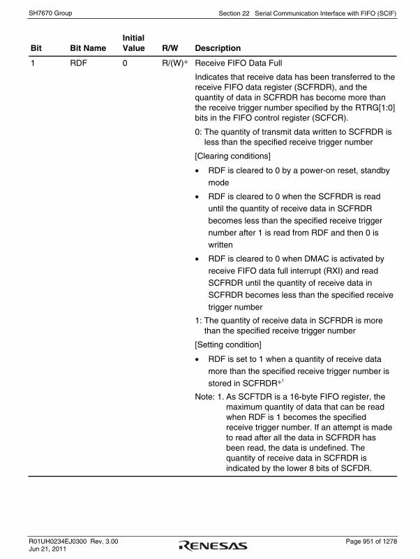
Section 22 Serial Communication Interface with FIFO (SCIF)
R01UH0234EJ0300 Rev. 3.00 Page 951 of 1278 Jun 21, 2011
SH7670 Group
Bit Bit Name Initial Value R/W Description
1 RDF 0 R/(W)* Receive FIFO Data Full
Indicates that receive data has been transferred to the receive FIFO data register (SCFRDR), and the quantity of data in SCFRDR has become more than the receive trigger number specified by the RTRG[1:0] bits in the FIFO control register (SCFCR).
0: The quantity of transmit data written to SCFRDR is less than the specified receive trigger number
[Clearing conditions]
• RDF is cleared to 0 by a power-on reset, standby
mode
• RDF is cleared to 0 when the SCFRDR is read until the quantity of receive data in SCFRDR
becomes less than the specified receive trigger
number after 1 is read from RDF and then 0 is
written
• RDF is cleared to 0 when DMAC is activated by
receive FIFO data full interrupt (RXI) and read
SCFRDR until the quantity of receive data in SCFRDR becomes less than the specified receive
trigger number
1: The quantity of receive data in SCFRDR is more than the specified receive trigger number
[Setting condition]
• RDF is set to 1 when a quantity of receive data
more than the specified receive trigger number is
stored in SCFRDR*1
Note: 1. As SCFTDR is a 16-byte FIFO register, the maximum quantity of data that can be read when RDF is 1 becomes the specified receive trigger number. If an attempt is made to read after all the data in SCFRDR has been read, the data is undefined. The quantity of receive data in SCFRDR is indicated by the lower 8 bits of SCFDR.
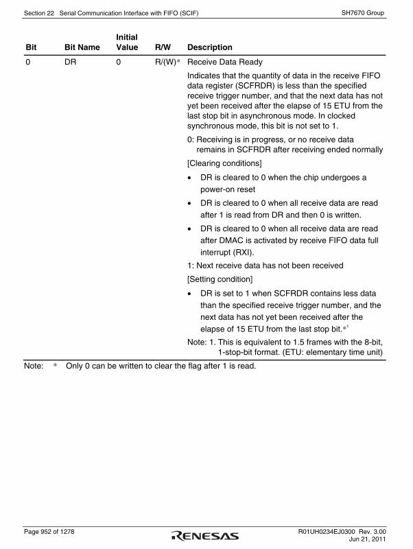
Section 22 Serial Communication Interface with FIFO (SCIF)
Page 952 of 1278 R01UH0234EJ0300 Rev. 3.00 Jun 21, 2011
SH7670 Group
Bit Bit Name Initial Value R/W Description
0 DR 0 R/(W)* Receive Data Ready
Indicates that the quantity of data in the receive FIFO data register (SCFRDR) is less than the specified receive trigger number, and that the next data has not yet been received after the elapse of 15 ETU from the last stop bit in asynchronous mode. In clocked synchronous mode, this bit is not set to 1.
0: Receiving is in progress, or no receive data remains in SCFRDR after receiving ended normally
[Clearing conditions]
• DR is cleared to 0 when the chip undergoes a
power-on reset
• DR is cleared to 0 when all receive data are read
after 1 is read from DR and then 0 is written.
• DR is cleared to 0 when all receive data are read after DMAC is activated by receive FIFO data full
interrupt (RXI).
1: Next receive data has not been received
[Setting condition]
• DR is set to 1 when SCFRDR contains less data
than the specified receive trigger number, and the next data has not yet been received after the
elapse of 15 ETU from the last stop bit.*1
Note: 1. This is equivalent to 1.5 frames with the 8-bit, 1-stop-bit format. (ETU: elementary time unit)
Note: * Only 0 can be written to clear the flag after 1 is read.

Section 22 Serial Communication Interface with FIFO (SCIF)
R01UH0234EJ0300 Rev. 3.00 Page 953 of 1278 Jun 21, 2011
SH7670 Group
22.3.8 Bit Rate Register (SCBRR)
SCBRR is an 8-bit register that, together with the baud rate generator clock source selected by the CKS[1:0] bits in the serial mode register (SCSMR), determines the serial transmit/receive bit rate.
The CPU can always read and write to SCBRR. SCBRR is initialized to H'FF by a power-on reset. Each channel has independent baud rate generator control, so different values can be set in three channels.
7 6 5 4 3 2 1 0
1 1 1 1 1 1 1 1R/W R/W R/W R/W R/W R/W R/W R/W
Bit:
Initial value:R/W:
The SCBRR setting is calculated as follows:
• Asynchronous mode:
N = × 106 − 164 × 22n-1 × B
Pφ
• Clocked synchronous mode:
N = × 106 − 18 × 22n-1 × B
Pφ
B: Bit rate (bits/s) N: SCBRR setting for baud rate generator (0 ≤ N ≤ 255) (The setting must satisfy the electrical characteristics.) Pφ: Operating frequency for peripheral modules (MHz) n: Baud rate generator clock source (n = 0, 1, 2, 3) (for the clock sources and values of n, see table 22.3.)

Section 22 Serial Communication Interface with FIFO (SCIF)
Page 954 of 1278 R01UH0234EJ0300 Rev. 3.00 Jun 21, 2011
SH7670 Group
Table 22.3 SCSMR Settings
SCSMR Settings
n Clock Source CKS[1] CKS[0]
0 Pφ 0 0
1 Pφ/4 0 1
2 Pφ/16 1 0
3 Pφ/64 1 1
The bit rate error in asynchronous is given by the following formula:
Error (%) = − 1 × 100(N + 1) × B × 64 × 22n-1
Pφ × 106
Table 22.4 lists examples of SCBRR settings in asynchronous mode, and table 22.5 lists examples of SCBRR settings in clocked synchronous mode.
Table 22.4 Bit Rates and SCBRR Settings (Asynchronous Mode)
Pφ (MHz)
5 6 6.144
Bit Rate (bit/s) n N Error (%) n N Error (%) n N Error (%)
110 2 88 −0.25 2 106 −0.44 2 108 0.08
150 2 64 0.16 2 77 0.16 2 79 0.00
300 1 129 0.16 1 155 0.16 1 159 0.00
600 1 64 0.16 1 77 0.16 1 79 0.00
1200 0 129 0.16 0 155 0.16 0 159 0.00
2400 0 64 0.16 0 77 0.16 0 79 0.00
4800 0 32 −1.36 0 38 0.16 0 39 0.00
9600 0 15 1.73 0 19 −2.34 0 19 0.00
19200 0 7 1.73 0 9 −2.34 0 9 0.00
31250 0 4 0.00 0 5 0.00 0 5 2.40
38400 0 3 1.73 0 4 −2.34 0 4 0.00

Section 22 Serial Communication Interface with FIFO (SCIF)
R01UH0234EJ0300 Rev. 3.00 Page 955 of 1278 Jun 21, 2011
SH7670 Group
Pφ (MHz)
7.3728 8 9.8304
Bit Rate (bit/s) n N Error (%) n N Error (%) n N Error (%)
110 2 130 –0.07 2 141 0.03 2 174 –0.26
150 2 95 0.00 2 103 0.16 2 127 0.00
300 1 191 0.00 1 207 0.16 1 255 0.00
600 1 95 0.00 1 103 0.16 1 127 0.00
1200 0 191 0.00 0 207 0.16 0 255 0.00
2400 0 95 0.00 0 103 0.16 0 127 0.00
4800 0 47 0.00 0 51 0.16 0 63 0.00
9600 0 23 0.00 0 25 0.16 0 31 0.00
19200 0 11 0.00 0 12 0.16 0 15 0.00
31250 0 6 5.33 0 7 0.00 0 9 –1.70
38400 0 5 0.00 0 6 –6.99 0 7 0.00
Pφ (MHz)
10 12 12.288 14.7456
Bit Rate (bit/s) n N
Error (%) n N
Error (%) n N
Error (%) n N
Error (%)
110 2 177 –0.25 2 212 0.03 2 217 0.08 3 64 0.70
150 2 129 0.16 2 155 0.16 2 159 0.00 2 191 0.00
300 2 64 0.16 2 77 0.16 2 79 0.00 2 95 0.00
600 1 129 0.16 1 155 0.16 1 159 0.00 1 191 0.00
1200 1 64 0.16 1 77 0.16 1 79 0.00 1 95 0.00
2400 0 129 0.16 0 155 0.16 0 159 0.00 0 191 0.00
4800 0 64 0.16 0 77 0.16 0 79 0.00 0 95 0.00
9600 0 32 –1.36 0 38 0.16 0 39 0.00 0 47 0.00
19200 0 15 1.73 0 19 0.16 0 19 0.00 0 23 0.00
31250 0 9 0.00 0 11 0.00 0 11 2.40 0 14 –1.70
38400 0 7 1.73 0 9 –2.34 0 9 0.00 0 11 0.00

Section 22 Serial Communication Interface with FIFO (SCIF)
Page 956 of 1278 R01UH0234EJ0300 Rev. 3.00 Jun 21, 2011
SH7670 Group
Pφ (MHz)
16 19.6608 20 24
Bit Rate (bit/s)
n
N
Error (%)
n
N
Error (%)
n
N
Error (%)
n
N
Error (%)
110 3 70 0.03 3 86 0.31 3 88 –0.25 3 106 –0.44
150 2 207 0.16 2 255 0.00 3 64 0.16 3 77 0.16
300 2 103 0.16 2 127 0.00 2 129 0.16 2 155 0.16
600 1 207 0.16 1 255 0.00 2 64 0.16 2 77 0.16
1200 1 103 0.16 1 127 0.00 1 129 0.16 1 155 0.16
2400 0 207 0.16 0 255 0.00 1 64 0.16 1 77 0.16
4800 0 103 0.16 0 127 0.00 0 129 0.16 0 155 0.16
9600 0 51 0.16 0 63 0.00 0 64 0.16 0 77 0.16
19200 0 25 0.16 0 31 0.00 0 32 –1.36 0 38 0.16
31250 0 15 0.00 0 19 –1.70 0 19 0.00 0 23 0.00
38400 0 12 0.16 0 15 0.00 0 15 1.73 0 19 –2.34
Pφ (MHz)
24.576 28.7 30 33
Bit Rate (bit/s)
n
N
Error (%)
n
N
Error (%)
n
N
Error (%)
n
N
Error (%)
110 3 108 0.08 3 126 0.31 3 132 0.13 3 145 0.33
150 3 79 0.00 3 92 0.46 3 97 –0.35 3 106 0.39
300 2 159 0.00 2 186 –0.08 2 194 0.16 2 214 –0.07
600 2 79 0.00 2 92 0.46 2 97 –0.35 2 106 0.39
1200 1 159 0.00 1 186 –0.08 1 194 0.16 1 214 –0.07
2400 1 79 0.00 1 92 0.46 1 97 –0.35 1 106 0.39
4800 0 159 0.00 0 186 –0.08 0 194 –1.36 0 214 –0.07
9600 0 79 0.00 0 92 0.46 0 97 –0.35 0 106 0.39
19200 0 39 0.00 0 46 –0.61 0 48 –0.35 0 53 –0.54
31250 0 24 –1.70 0 28 –1.03 0 29 0.00 0 32 0.00
38400 0 19 0.00 0 22 1.55 0 23 1.73 0 26 –0.54

Section 22 Serial Communication Interface with FIFO (SCIF)
R01UH0234EJ0300 Rev. 3.00 Page 957 of 1278 Jun 21, 2011
SH7670 Group
Pφ (MHz)
50
Bit Rate (bit/s)
n
N
Error (%)
110 3 221 –0.02
150 3 162 –0.15
300 3 80 0.47
600 2 162 –0.15
1200 2 80 0.47
2400 1 162 –0.15
4800 1 80 0.47
9600 0 162 –0.15
19200 0 80 0.47
31250 0 49 0.00
38400 0 40 –0.76
Note: Settings with an error of 1% or less are recommended.
Table 22.5 Bit Rates and SCBRR Settings (Clocked Synchronous Mode)
Pφ (MHz)
5 8 16 28.7 30 33 50
Bit Rate (bit/s)
n N n N n N n N n N n N n N
110 — — — — — — — — — — — — — —
250 3 77 3 124 3 249 — — — — — — — —
500 3 38 2 249 3 124 3 223 3 233 3 255 — —
1k 2 77 2 124 2 249 3 111 3 116 3 125 3 194
2.5k 1 124 1 199 2 99 2 178 2 187 2 200 3 77
5k 0 249 1 99 1 199 2 89 2 93 2 100 2 155
10k 0 124 0 199 1 99 1 178 1 187 1 200 2 77
25k 0 49 0 79 0 159 1 71 1 74 1 80 1 124
50k 0 24 0 39 0 79 0 143 0 149 0 160 0 249
100k — — 0 19 0 39 0 71 0 74 0 80 0 124
250k 0 4 0 7 0 15 — — 0 29 0 31 0 49
500k — — 0 3 0 7 — — 0 14 0 15 0 24
1M — — 0 1 0 3 — — — — 0 7 0 12
2M 0 0* 0 1 — — — — — — — —

Section 22 Serial Communication Interface with FIFO (SCIF)
Page 958 of 1278 R01UH0234EJ0300 Rev. 3.00 Jun 21, 2011
SH7670 Group
[Legend]
Blank: No setting possible —: Setting possible, but error occurs
*: Continuous transmission/reception not possible
Table 22.6 indicates the maximum bit rates in asynchronous mode when the baud rate generator is used. Table 22.7 lists the maximum bit rates in asynchronous mode when the external clock input is used. Table 22.8 lists the maximum bit rates in clocked synchronous mode when the external clock input is used (when tScyc = 12tpcyc*).
Note: * Make sure that the electrical characteristics of this LSI and that of a connected LSI are satisfied.
Table 22.6 Maximum Bit Rates for Various Frequencies with Baud Rate Generator (Asynchronous Mode)
Settings
Pφ (MHz) Maximum Bit Rate (bits/s) n N
5 156250 0 0
8 250000 0 0
9.8304 307200 0 0
12 375000 0 0
14.7456 460800 0 0
16 500000 0 0
19.6608 614400 0 0
20 625000 0 0
24 750000 0 0
24.576 768000 0 0
28.7 896875 0 0
30 937500 0 0
33 1031250 0 0
50 1562500 0 0

Section 22 Serial Communication Interface with FIFO (SCIF)
R01UH0234EJ0300 Rev. 3.00 Page 959 of 1278 Jun 21, 2011
SH7670 Group
Table 22.7 Maximum Bit Rates with External Clock Input (Asynchronous Mode)
Pφ (MHz) External Input Clock (MHz) Maximum Bit Rate (bits/s)
5 1.2500 78125
8 2.0000 125000
9.8304 2.4576 153600
12 3.0000 187500
14.7456 3.6864 230400
16 4.0000 250000
19.6608 4.9152 307200
20 5.0000 312500
24 6.0000 375000
24.576 6.1440 384000
28.7 7.1750 448436
30 7.5000 468750
33 8.25 515625
50 12.5 781250
Table 22.8 Maximum Bit Rates with External Clock Input (Clocked Synchronous Mode, tScyc = 12tpcyc)
Pφ (MHz) External Input Clock (MHz) Maximum Bit Rate (bits/s)
5 0.4166 416666.6
8 0.6666 666666.6
16 1.3333 1333333.3
24 2.0000 2000000.0
28.7 2.3916 2391666.6
30 2.5000 2500000.0
33 2.7500 2750000.0
50 4.1667 4166666.7

Section 22 Serial Communication Interface with FIFO (SCIF)
Page 960 of 1278 R01UH0234EJ0300 Rev. 3.00 Jun 21, 2011
SH7670 Group
22.3.9 FIFO Control Register (SCFCR)
SCFCR resets the quantity of data in the transmit and receive FIFO data registers, sets the trigger data quantity, and contains an enable bit for loop-back testing. SCFCR can always be read and written to by the CPU. It is initialized to H'0000 by a power-on reset.
15 14 13 12 11 10 9 8 7 6 5 4 3 2 1 0
0 0 0 0 0 0 0 0 0 0 0 0 0 0 0 0R R R R R R/W R/W R/W R/W R/W R/W R/W R/W R/W R/W R/W
Bit:
Initial value:R/W:
- - - - - RSTRG[2:0] RTRG[1:0] TTRG[1:0] MCE TFRST RFRST LOOP
Bit Bit Name Initial Value R/W Description
15 to 11 — All 0 R Reserved
These bits are always read as 0. The write value should always be 0.
10 to 8 RSTRG[2:0] 000 R/W RTS Output Active Trigger
When the quantity of receive data in receive FIFO data register (SCFRDR) becomes more than the number shown below, RTS signal is set to high.
000: 15
001: 1
010: 4
011: 6
100: 8
101: 10
110: 12
111: 14

Section 22 Serial Communication Interface with FIFO (SCIF)
R01UH0234EJ0300 Rev. 3.00 Page 961 of 1278 Jun 21, 2011
SH7670 Group
Bit Bit Name Initial Value R/W Description
Receive FIFO Data Trigger
Set the quantity of receive data which sets the receive data full (RDF) flag in the serial status register (SCFSR). The RDF flag is set to 1 when the quantity of receive data stored in the receive FIFO register (SCFRDR) is increased more than the set trigger number shown below.
• Asynchronous mode • Clocked synchronous mode
00: 1
01: 4
10: 8
11: 14
00: 1
01: 2
10: 8
11: 14
7, 6 RTRG[1:0] 00 R/W
Note: In clock synchronous mode, to transfer the receive data using DMAC, set the receive trigger number to 1. If set to other than 1, CPU must read the receive data left in SCFRDR.
5, 4 TTRG[1:0] 00 R/W Transmit FIFO Data Trigger
Set the quantity of remaining transmit data which sets the transmit FIFO data register empty (TDFE) flag in the serial status register (SCFSR). The TDFE flag is set to 1 when the quantity of transmit data in the transmit FIFO data register (SCFTDR) becomes less than the set trigger number shown below.
00: 8 (8)*
01: 4 (12)*
10: 2 (14)*
11: 0 (16)*
Note: * Values in parentheses mean the number of empty bytes in SCFTDR when the TDFE flag is set to 1.

Section 22 Serial Communication Interface with FIFO (SCIF)
Page 962 of 1278 R01UH0234EJ0300 Rev. 3.00 Jun 21, 2011
SH7670 Group
Bit Bit Name Initial Value R/W Description
3 MCE 0 R/W Modem Control Enable
Enables modem control signals CTS and RTS.
In clocked synchronous mode, the MCE bit should always be 0.
0: Modem signal disabled*
1: Modem signal enabled
Note: * CTS is fixed at active 0 regardless of the input value, and RTS is also fixed at 0.
2 TFRST 0 R/W Transmit FIFO Data Register Reset
Disables the transmit data in the transmit FIFO data register and resets the data to the empty state.
0: Reset operation disabled*
1: Reset operation enabled
Note: * Reset operation is executed by a power-on reset.
1 RFRST 0 R/W Receive FIFO Data Register Reset
Disables the receive data in the receive FIFO data register and resets the data to the empty state.
0: Reset operation disabled*
1: Reset operation enabled
Note: * Reset operation is executed by a power-on reset.
0 LOOP 0 R/W Loop-Back Test
Internally connects the transmit output pin (TxD) and receive input pin (RxD) and internally connects the RTS pin and CTS pin and enables loop-back testing.
0: Loop back test disabled
1: Loop back test enabled

Section 22 Serial Communication Interface with FIFO (SCIF)
R01UH0234EJ0300 Rev. 3.00 Page 963 of 1278 Jun 21, 2011
SH7670 Group
22.3.10 FIFO Data Count Set Register (SCFDR)
SCFDR is a 16-bit register which indicates the quantity of data stored in the transmit FIFO data register (SCFTDR) and the receive FIFO data register (SCFRDR).
It indicates the quantity of transmit data in SCFTDR with the upper 8 bits, and the quantity of receive data in SCFRDR with the lower 8 bits. SCFDR can always be read by the CPU. SCFDR is initialized to H'0000 by a power on reset.
15 14 13 12 11 10 9 8 7 6 5 4 3 2 1 0
0 0 0 0 0 0 0 0 0 0 0 0 0 0 0 0R R R R R R R R R R R R R R R R
Bit:
Initial value:R/W:
- - - T[4:0] - - - R[4:0]
Bit Bit Name Initial Value R/W Description
15 to 13 — All 0 R Reserved
These bits are always read as 0. The write value should always be 0.
12 to 8 T[4:0] 00000 R T4 to T0 bits indicate the quantity of non-transmitted data stored in SCFTDR. H'00 means no transmit data, and H'10 means that SCFTDR is full of transmit data.
7 to 5 — All 0 R Reserved
These bits are always read as 0. The write value should always be 0.
4 to 0 R[4:0] 00000 R R4 to R0 bits indicate the quantity of receive data stored in SCFRDR. H'00 means no receive data, and H'10 means that SCFRDR full of receive data.
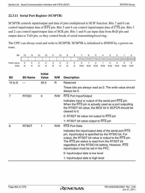
Section 22 Serial Communication Interface with FIFO (SCIF)
Page 964 of 1278 R01UH0234EJ0300 Rev. 3.00 Jun 21, 2011
SH7670 Group
22.3.11 Serial Port Register (SCSPTR)
SCSPTR controls input/output and data of pins multiplexed to SCIF function. Bits 7 and 6 can control input/output data of RTS pin. Bits 5 and 4 can control input/output data of CTS pin. Bits 3 and 2 can control input/output data of SCK pin. Bits 1 and 0 can input data from RxD pin and output data to TxD pin, so they control break of serial transmitting/receiving.
The CPU can always read and write to SCSPTR. SCSPTR is initialized to H'0050 by a power-on reset.
15 14 13 12 11 10 9 8 7 6 5 4 3 2 1 0
0 0 0 0 0 0 0 0 0 1 0 1 0 0 0 0R R R R R R R R R/W R/W R/W R/W R/W R/W R/W R/W
Bit:
Initial value:R/W:
- - - - - - - - RTSIO RTSDT CTSIO CTSDT SCKIO SCKDT SPB2IOSPB2DT
Bit Bit Name Initial Value R/W Description
15 to 8 — All 0 R Reserved
These bits are always read as 0. The write value should always be 0.
7 RTSIO 0 R/W RTS Port Input/Output
Indicates input or output of the serial port RTS pin. When the RTS pin is actually used as a port outputting the RTSDT bit value, the MCE bit in SCFCR should be cleared to 0.
0: RTSDT bit value not output to RTS pin
1: RTSDT bit value output to RTS pin
6 RTSDT 1 R/W RTS Port Data
Indicates the input/output data of the serial port RTS pin. Input/output is specified by the RTSIO bit. For output, the RTSDT bit value is output to the RTS pin. The RTS pin status is read from the RTSDT bit regardless of the RTSIO bit setting. However, RTS input/output must be set in the PFC.
0: Input/output data is low level
1: Input/output data is high level

Section 22 Serial Communication Interface with FIFO (SCIF)
R01UH0234EJ0300 Rev. 3.00 Page 965 of 1278 Jun 21, 2011
SH7670 Group
Bit Bit Name Initial Value R/W Description
5 CTSIO 0 R/W CTS Port Input/Output
Indicates input or output of the serial port CTS pin. When the CTS pin is actually used as a port outputting the CTSDT bit value, the MCE bit in SCFCR should be cleared to 0.
0: CTSDT bit value not output to CTS pin
1: CTSDT bit value output to CTS pin
4 CTSDT 1 R/W CTS Port Data
Indicates the input/output data of the serial port CTS pin. Input/output is specified by the CTSIO bit. For output, the CTSDT bit value is output to the CTS pin. The CTS pin status is read from the CTSDT bit regardless of the CTSIO bit setting. However, CTS input/output must be set in the PFC.
0: Input/output data is low level
1: Input/output data is high level
3 SCKIO 0 R/W SCK Port Input/Output
Indicates input or output of the serial port SCK pin. When the SCK pin is actually used as a port outputting the SCKDT bit value, the CKE[1:0] bits in SCSCR should be cleared to 0.
0: SCKDT bit value not output to SCK pin
1: SCKDT bit value output to SCK pin
2 SCKDT 0 R/W SCK Port Data
Indicates the input/output data of the serial port SCK pin. Input/output is specified by the SCKIO bit. For output, the SCKDT bit value is output to the SCK pin. The SCK pin status is read from the SCKDT bit regardless of the SCKIO bit setting. However, SCK input/output must be set in the PFC.
0: Input/output data is low level
1: Input/output data is high level

Section 22 Serial Communication Interface with FIFO (SCIF)
Page 966 of 1278 R01UH0234EJ0300 Rev. 3.00 Jun 21, 2011
SH7670 Group
Bit Bit Name Initial Value R/W Description
1 SPB2IO 0 R/W Serial Port Break Input/Output
Indicates input or output of the serial port TxD pin. When the TxD pin is actually used as a port outputting the SPB2DT bit value, the TE bit in SCSCR should be cleared to 0.
0: SPB2DT bit value not output to TxD pin
1: SPB2DT bit value output to TxD pin
0 SPB2DT 0 R/W Serial Port Break Data
Indicates the input data of the RxD pin and the output data of the TxD pin used as serial ports. Input/output is specified by the SPB2IO bit. When the TxD pin is set to output, the SPB2DT bit value is output to the TxD pin. The RxD pin status is read from the SPB2DT bit regardless of the SPB2IO bit setting. However, RxD input and TxD output must be set in the PFC.
0: Input/output data is low level
1: Input/output data is high level

Section 22 Serial Communication Interface with FIFO (SCIF)
R01UH0234EJ0300 Rev. 3.00 Page 967 of 1278 Jun 21, 2011
SH7670 Group
22.3.12 Line Status Register (SCLSR)
The CPU can always read or write to SCLSR, but cannot write 1 to the ORER flag. This flag can be cleared to 0 only if it has first been read (after being set to 1).
SCLSR is initialized to H'0000 by a power-on reset.
15 14 13 12 11 10 9 8 7 6 5 4 3 2 1 0
0 0 0 0 0 0 0 0 0 0 0 0 0 0 0 0R R R R R R R R R R R R R R R R/(W)*
Bit:
Initial value:R/W:
Note: Only 0 can be written to clear the flag after 1 is read.*
- - - - - - - - - - - - - - - ORER
Bit Bit Name Initial Value R/W Description
15 to 1 — All 0 R Reserved
These bits are always read as 0. The write value should always be 0.
0 ORER 0 R/(W)* Overrun Error
Indicates the occurrence of an overrun error.
0: Receiving is in progress or has ended normally*1
[Clearing conditions]
• ORER is cleared to 0 when the chip is a power-on reset
• ORER is cleared to 0 when 0 is written after 1 is read from ORER.
1: An overrun error has occurred*2
[Setting condition]
• ORER is set to 1 when the next serial receiving is finished while the receive FIFO is full of 16-byte receive data.
Notes: 1. Clearing the RE bit to 0 in SCSCR does not affect the ORER bit, which retains its previous value.
2. The receive FIFO data register (SCFRDR) retains the data before an overrun error has occurred, and the next received data is discarded. When the ORER bit is set to 1, the SCIF cannot continue the next serial reception.

Section 22 Serial Communication Interface with FIFO (SCIF)
Page 968 of 1278 R01UH0234EJ0300 Rev. 3.00 Jun 21, 2011
SH7670 Group
22.4 Operation
22.4.1 Overview
For serial communication, the SCIF has an asynchronous mode in which characters are synchronized individually, and a clocked synchronous mode in which communication is synchronized with clock pulses.
The SCIF has a 16-stage FIFO buffer for both transmission and receptions, reducing the overhead of the CPU, and enabling continuous high-speed communication. Furthermore, RTS and CTS signals are provided as modem control signals.
Furthermore, RTS and CTS signals are provided as modem control signals.
The transmission format is selected in the serial mode register (SCSMR), as shown in table 22.9. The SCIF clock source is selected by the combination of the CKE[1:0] bits in the serial control register (SCSCR), as shown in table 22.10.
(1) Asynchronous Mode
• Data length is selectable: 7 or 8 bits
• Parity bit is selectable. So is the stop bit length (1 or 2 bits). The combination of the preceding selections constitutes the communication format and character length.
• In receiving, it is possible to detect framing errors, parity errors, receive FIFO data full, overrun errors, receive data ready, and breaks.
• The number of stored data bytes is indicated for both the transmit and receive FIFO registers.
• An internal or external clock can be selected as the SCIF clock source.
⎯ When an internal clock is selected, the SCIF operates using the clock of on-chip baud rate generator.
⎯ When an external clock is selected, the external clock input must have a frequency 16 times the bit rate. (The on-chip baud rate generator is not used.)
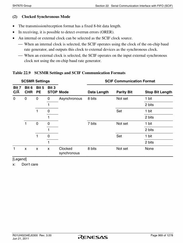
Section 22 Serial Communication Interface with FIFO (SCIF)
R01UH0234EJ0300 Rev. 3.00 Page 969 of 1278 Jun 21, 2011
SH7670 Group
(2) Clocked Synchronous Mode
• The transmission/reception format has a fixed 8-bit data length.
• In receiving, it is possible to detect overrun errors (ORER).
• An internal or external clock can be selected as the SCIF clock source.
⎯ When an internal clock is selected, the SCIF operates using the clock of the on-chip baud rate generator, and outputs this clock to external devices as the synchronous clock.
⎯ When an external clock is selected, the SCIF operates on the input external synchronous clock not using the on-chip baud rate generator.
Table 22.9 SCSMR Settings and SCIF Communication Formats
SCSMR Settings SCIF Communication Format
Bit 7 C/A
Bit 6 CHR
Bit 5 PE
Bit 3 STOP
Mode Data Length Parity Bit Stop Bit Length
0 0 0 0 8 bits Not set 1 bit
1 2 bits
1 0 Set 1 bit
1 2 bits
1 0 0 7 bits Not set 1 bit
1 2 bits
1 0 Set 1 bit
1
Asynchronous
2 bits
1 x x x Clocked synchronous
8 bits Not set None
[Legend]
x: Don't care

Section 22 Serial Communication Interface with FIFO (SCIF)
Page 970 of 1278 R01UH0234EJ0300 Rev. 3.00 Jun 21, 2011
SH7670 Group
Table 22.10 SCSMR and SCSCR Settings and SCIF Clock Source Selection
SCSMR SCSCR SCIF Transmit/Receive Clock
Bit 7 C/A Bit 1, 0 CKE[1:0]
Mode
Clock Source
SCK Pin Function
00 SCIF does not use the SCK pin
01
Internal
Outputs a clock with a frequency 16 times the bit rate
10 External Inputs a clock with frequency 16 times the bit rate
0
11
Asynchronous
Setting prohibited
0x Internal Outputs the serial clock
10 External Inputs the serial clock 1
11
Clocked synchronous
Setting prohibited
[Legend]
x: Don't care

Section 22 Serial Communication Interface with FIFO (SCIF)
R01UH0234EJ0300 Rev. 3.00 Page 971 of 1278 Jun 21, 2011
SH7670 Group
22.4.2 Operation in Asynchronous Mode
In asynchronous mode, each transmitted or received character begins with a start bit and ends with a stop bit. Serial communication is synchronized one character at a time.
The transmitting and receiving sections of the SCIF are independent, so full duplex communication is possible. The transmitter and receiver are 16-byte FIFO buffered, so data can be written and read while transmitting and receiving are in progress, enabling continuous transmitting and receiving.
Figure 22.2 shows the general format of asynchronous serial communication.
In asynchronous serial communication, the communication line is normally held in the mark (high) state. The SCIF monitors the line and starts serial communication when the line goes to the space (low) state, indicating a start bit. One serial character consists of a start bit (low), data (LSB first), parity bit (high or low), and stop bit (high), in that order.
When receiving in asynchronous mode, the SCIF synchronizes at the falling edge of the start bit. The SCIF samples each data bit on the eighth pulse of a clock with a frequency 16 times the bit rate. Receive data is latched at the center of each bit.
0
1
D0 D1 D3 D4 D5 D6D2 0/1 1 1
1
D7
(LSB) (MSB)
Start bit
Idle state (mark state)
Stop bit
Transmit/receive data
Serial data
Parity bit
1 bit 1 or 2 bits7 or 8 bits 1 bit
or none
One unit of transfer data (character or frame)
Figure 22.2 Example of Data Format in Asynchronous Communication (8-Bit Data with Parity and Two Stop Bits)
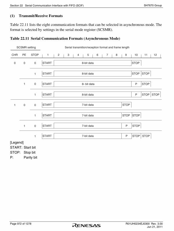
Section 22 Serial Communication Interface with FIFO (SCIF)
Page 972 of 1278 R01UH0234EJ0300 Rev. 3.00 Jun 21, 2011
SH7670 Group
(1) Transmit/Receive Formats
Table 22.11 lists the eight communication formats that can be selected in asynchronous mode. The format is selected by settings in the serial mode register (SCSMR).
Table 22.11 Serial Communication Formats (Asynchronous Mode)
SCSMR setting
CHR PE STOP
0 0 0 START 8-bit data STOP
0
1
1
1
1 0 0
1 0
1
1
1 2 3 4 5 6 7 8 9 10 11 12
Serial transmition/reception format and frame length
START 8-bit data STOP STOP
START 8- bit data P STOP
START 8-bit data P STOP STOP
START 7-bit data STOP
START 7-bit data STOP STOP
START 7-bit data P STOP
START 7-bit data P STOP STOP [Legend]
START: Start bit STOP: Stop bit
P: Parity bit

Section 22 Serial Communication Interface with FIFO (SCIF)
R01UH0234EJ0300 Rev. 3.00 Page 973 of 1278 Jun 21, 2011
SH7670 Group
(2) Clock
An internal clock generated by the on-chip baud rate generator or an external clock input from the SCK pin can be selected as the SCIF transmit/receive clock. The clock source is selected by the C/A bit in the serial mode register (SCSMR) and bits CKE[1:0] in the serial control register (SCSCR). For clock source selection, refer to table 22.10, SCSMR and SCSCR Settings and SCIF Clock Source Selection.
When an external clock is input at the SCK pin, it must have a frequency equal to 16 times the desired bit rate.
When the SCIF operates on an internal clock, it can output a clock signal on the SCK pin. The frequency of this output clock is 16 times the desired bit rate.
(3) Transmitting and Receiving Data
• SCIF Initialization (Asynchronous Mode)
Before transmitting or receiving, clear the TE and RE bits to 0 in the serial control register (SCSCR), then initialize the SCIF as follows.
When changing the operation mode or the communication format, always clear the TE and RE bits to 0 before following the procedure given below. Clearing TE to 0 initializes the transmit shift register (SCTSR). Clearing TE and RE to 0, however, does not initialize the serial status register (SCFSR), transmit FIFO data register (SCFTDR), or receive FIFO data register (SCFRDR), which retain their previous contents. Clear TE to 0 after all transmit data has been transmitted and the TEND flag in the SCFSR is set. The TE bit can be cleared to 0 during transmission, but the transmit data goes to the Mark state after the bit is cleared to 0. Set the TFRST bit in SCFCR to 1 and reset SCFTDR before TE is set again to start transmission.
When an external clock is used, the clock should not be stopped during initialization or subsequent operation. SCIF operation becomes unreliable if the clock is stopped.

Section 22 Serial Communication Interface with FIFO (SCIF)
Page 974 of 1278 R01UH0234EJ0300 Rev. 3.00 Jun 21, 2011
SH7670 Group
Figure 22.3 shows a sample flowchart for initializing the SCIF.
Start of initialization
Clear TE and RE bits in SCSCR to 0
Set TFRST and RFRST bits in SCFCR to 1
Set CKE[1:0] in SCSCR(leaving TIE, RIE, TE, and RE bits cleared to 0)
Set data transfer format in SCSMR
Set value in SCBRR
Set RTRG[1:0], TTRG[1:0], and MCE bits inSCFCR, and clear TFRST and RFRST bits to 0
PFC setting for external pins usedSCK, TxD, RxD
Set TE and RE bits in SCSCR to 1, and set TIE, RIE, and REIE bits
End of initialization
Set the clock selection in SCSCR.Be sure to clear bits TIE, RIE, TE, and RE to 0.
Set the data transfer format in SCSMR.
Write a value corresponding to the bit rate into SCBRR. (Not necessary if an external clock is used.)
Sets PFC for external pins used.Set as RxD input at receiving andTxD at transmission.However, no setting for SCK pin isrequired when CKE[1:0] is 00.In the case when internal synchronousclock output is set, the SCK pin startsoutputting the clock at this stage.
Set the TE bit or RE bit in SCSCR to 1. Also set the RIE, REIE, and TIE bits. Setting the TE and RE bitsenables the TxD and RxD pins to beused. When transmitting, the SCIF will go to the mark state; when receiving, it will go to the idle state, waiting for a start bit.
[1]
[1]
[2]
[3]
[4]
[5]
[2]
[3]
[4]
[5]
After reading ER, DR, and BRK flags in SCFSR,and each flag in SCLSR, write 0 to clear them
Figure 22.3 Sample Flowchart for SCIF Initialization

Section 22 Serial Communication Interface with FIFO (SCIF)
R01UH0234EJ0300 Rev. 3.00 Page 975 of 1278 Jun 21, 2011
SH7670 Group
• Transmitting Serial Data (Asynchronous Mode)
Figure 22.4 shows a sample flowchart for serial transmission.
Use the following procedure for serial data transmission after enabling the SCIF for transmission.
Start of transmission
Read TDFE flag in SCFSR
TDFE = 1?
Write transmit data in SCFTDR,and read 1 from TDFE flag and TEND flag in SCFSR,
then clear to 0
All data transmitted?
Read TEND flag in SCFSR
TEND = 1?
Break output?
Clear SPB2DT to 0 andset SPB2IO to 1
Clear TE bit in SCSCR to 0
End of transmission
No
Yes
No
Yes
No
Yes
No
Yes
[1] SCIF status check and transmit data write: Read SCFSR and check that the TDFE flag is set to 1, then write transmit data to SCFTDR, and read 1 from the TDFE and TEND flags, then clear to 0. The quantity of transmit data that can be written is 16 - (transmit trigger set number).
[2] Serial transmission continuation procedure: To continue serial transmission, read 1 from the TDFE flag to confirm that writing is possible, then write data to SCFTDR, and then clear the TDFE flag to 0.
[3] Break output during serial transmission: To output a break in serial transmission, clear the SPB2DT bit to 0 and set the SPB2IO bit to 1 in SCSPTR, then clear the TE bit in SCSCR to 0.
In [1] and [2], it is possible to ascertain the number of data bytes that can be written from the number of transmit data bytes in SCFTDR indicated by the upper 8 bits of SCFDR.
[1]
[2]
[3]
Figure 22.4 Sample Flowchart for Transmitting Serial Data

Section 22 Serial Communication Interface with FIFO (SCIF)
Page 976 of 1278 R01UH0234EJ0300 Rev. 3.00 Jun 21, 2011
SH7670 Group
In serial transmission, the SCIF operates as described below.
1. When data is written into the transmit FIFO data register (SCFTDR), the SCIF transfers the data from SCFTDR to the transmit shift register (SCTSR) and starts transmitting. Confirm that the TDFE flag in the serial status register (SCFSR) is set to 1 before writing transmit data to SCFTDR. The number of data bytes that can be written is (16 – transmit trigger setting).
2. When data is transferred from SCFTDR to SCTSR and transmission is started, consecutive transmit operations are performed until there is no transmit data left in SCFTDR. When the number of transmit data bytes in SCFTDR falls below the transmit trigger number set in the FIFO control register (SCFCR), the TDFE flag is set. If the TIE bit in the serial control register (SCSR) is set to 1 at this time, a transmit-FIFO-data-empty interrupt (TXI) request is generated.
The serial transmit data is sent from the TxD pin in the following order.
A. Start bit: One-bit 0 is output.
B. Transmit data: 8-bit or 7-bit data is output in LSB-first order.
C. Parity bit: One parity bit (even or odd parity) is output. (A format in which a parity bit is not output can also be selected.)
D. Stop bit(s): One or two 1 bits (stop bits) are output.
E. Mark state: 1 is output continuously until the start bit that starts the next transmission is sent.
3. The SCIF checks the SCFTDR transmit data at the timing for sending the stop bit. If data is present, the data is transferred from SCFTDR to SCTSR, the stop bit is sent, and then serial transmission of the next frame is started.

Section 22 Serial Communication Interface with FIFO (SCIF)
R01UH0234EJ0300 Rev. 3.00 Page 977 of 1278 Jun 21, 2011
SH7670 Group
Figure 22.5 shows an example of the operation for transmission.
TDFE
0 0/1 1
1 1
D0 D1 D7 0 0/1 1D0 D1 D7
TEND
Serial data
Start bit Data
Parity bit
Stop bit
Start bit
Idle state (mark state)
DataParity bit
Stop bit
TXI interrupt request
Data written to SCFTDR and TDFE flag read as 1 then cleared to 0 by TXI interrupt handler
One frame
TXI interrupt request
Figure 22.5 Example of Transmit Operation (8-Bit Data, Parity, 1 Stop Bit)
4. When modem control is enabled, transmission can be stopped and restarted in accordance with the CTS input value. When CTS is set to 1, if transmission is in progress, the line goes to the mark state after transmission of one frame. When CTS is set to 0, the next transmit data is output starting from the start bit.
Figure 22.6 shows an example of the operation when modem control is used.
CTS
0 0/1D0 D1 D7 0 0/1D0 D1 D7Serial dataTxD
Drive high before stop bit
Startbit
Paritybit
Stopbit
Startbit
Figure 22.6 Example of Operation Using Modem Control (CTS)

Section 22 Serial Communication Interface with FIFO (SCIF)
Page 978 of 1278 R01UH0234EJ0300 Rev. 3.00 Jun 21, 2011
SH7670 Group
• Receiving Serial Data (Asynchronous Mode)
Figures 22.7 and 22.8 show sample flowcharts for serial reception.
Use the following procedure for serial data reception after enabling the SCIF for reception.
Start of reception
Read ER, DR, BRK flags inSCFSR and ORER
flag in SCLSR
ER, DR, BRK or ORER = 1?
Read RDF flag in SCFSR
RDF = 1?
Read receive data inSCFRDR, and clear RDF
flag in SCFSR to 0
All data received?
Clear RE bit in SCSCR to 0
End of reception
Yes
No
Yes
Yes
No
No
Error handling
[1] Receive error handling and break detection:
Read the DR, ER, and BRK flags in SCFSR, and the ORER flag in SCLSR, to identify any error, perform the appropriate error handling, then clear the DR, ER, BRK, and ORER flags to 0. In the case of a framing error, a break can also be detected by reading the value of the RxD pin.
[2] SCIF status check and receive data read:
Read SCFSR and check that RDF flag = 1, then read the receive data in SCFRDR, read 1 from the RDF flag, and then clear the RDF flag to 0. The transition of the RDF flag from 0 to 1 can also be identified by a receive FIFO data full interrupt (RXI).
[3] Serial reception continuation procedure:
To continue serial reception, read at least the receive trigger set number of receive data bytes from SCFRDR, read 1 from the RDF flag, then clear the RDF flag to 0. The number of receive data bytes in SCFRDR can be ascertained by reading from SCRFDR.
[1]
[2]
[3]
Figure 22.7 Sample Flowchart for Receiving Serial Data

Section 22 Serial Communication Interface with FIFO (SCIF)
R01UH0234EJ0300 Rev. 3.00 Page 979 of 1278 Jun 21, 2011
SH7670 Group
Error handling
Receive error handling
ER = 1?
BRK = 1?
Break handling
DR = 1?
Read receive data in SCFRDR
Clear DR, ER, BRK flags in SCFSR,
and ORER flag in SCLSR to 0
End
Yes
Yes
Yes
No
Overrun error handling
ORER = 1?
Yes
No
No
No
• Whether a framing error or parity error has occurred in the receive data that is to be read from the receive FIFO data register (SCFRDR) can be ascertained from the FER and PER bits in the serial status register (SCFSR).
• When a break signal is received, receive data is not transferred to SCFRDR while the BRK flag is set. However, note that the last data in SCFRDR is H'00, and the break data in which a framing error occurred is stored.
Figure 22.8 Sample Flowchart for Receiving Serial Data (cont)

Section 22 Serial Communication Interface with FIFO (SCIF)
Page 980 of 1278 R01UH0234EJ0300 Rev. 3.00 Jun 21, 2011
SH7670 Group
In serial reception, the SCIF operates as described below.
1. The SCIF monitors the transmission line, and if a 0 start bit is detected, performs internal synchronization and starts reception.
2. The received data is stored in SCRSR in LSB-to-MSB order.
3. The parity bit and stop bit are received. After receiving these bits, the SCIF carries out the following checks.
A. Stop bit check: The SCIF checks whether the stop bit is 1. If there are two stop bits, only the first is checked.
B. The SCIF checks whether receive data can be transferred from the receive shift register (SCRSR) to SCFRDR.
C. Overrun check: The SCIF checks that the ORER flag is 0, indicating that the overrun error has not occurred.
D. Break check: The SCIF checks that the BRK flag is 0, indicating that the break state is not set.
If all the above checks are passed, the receive data is stored in SCFRDR.
Note: When a parity error or a framing error occurs, reception is not suspended.
4. If the RIE bit in SCSCR is set to 1 when the RDF or DR flag changes to 1, a receive-FIFO-data-full interrupt (RXI) request is generated. If the RIE bit or the REIE bit in SCSCR is set to 1 when the ER flag changes to 1, a receive-error interrupt (ERI) request is generated. If the RIE bit or the REIE bit in SCSCR is set to 1 when the BRK or ORER flag changes to 1, a break reception interrupt (BRI) request is generated.
Figure 22.9 shows an example of the operation for reception.

Section 22 Serial Communication Interface with FIFO (SCIF)
R01UH0234EJ0300 Rev. 3.00 Page 981 of 1278 Jun 21, 2011
SH7670 Group
RDF
0 0/1 1
1 1
D0 D1 D7 0 0/1 1D0 D1 D7
FER
Serial data
Start bit
Data Parity bit
Stop bit
Start bit
Data Parity bit
Stop bit
RXI interrupt request
One frameData read and RDF flag read as 1 then cleared to 0 by RXI interrupt handler
ERI interrupt request generated by receive error
Idle state (mark state)
Figure 22.9 Example of SCIF Receive Operation (8-Bit Data, Parity, 1 Stop Bit)
5. When modem control is enabled, the RTS signal is output when SCFRDR is empty. When RTS is 0, reception is possible. When RTS is 1, this indicates that SCFRDR exceeds the number set for the RTS output active trigger.
Figure 22.10 shows an example of the operation when modem control is used.
RTS
0 10/1D0 D1 D2 D7 D0 D1 D1D70Serial data
RxD
Start bit
Paritybit
Start bit
Figure 22.10 Example of Operation Using Modem Control (RTS)

Section 22 Serial Communication Interface with FIFO (SCIF)
Page 982 of 1278 R01UH0234EJ0300 Rev. 3.00 Jun 21, 2011
SH7670 Group
22.4.3 Operation in Clocked Synchronous Mode
In clocked synchronous mode, the SCIF transmits and receives data in synchronization with clock pulses. This mode is suitable for high-speed serial communication.
The SCIF transmitter and receiver are independent, so full-duplex communication is possible while sharing the same clock. The transmitter and receiver are also 16-byte FIFO buffered, so continuous transmitting or receiving is possible by reading or writing data while transmitting or receiving is in progress.
Figure 22.11 shows the general format in clocked synchronous serial communication.
Bit 0 Bit 1 Bit 2 Bit 3 Bit 4 Bit 5 Bit 6 Bit 7
* *
LSB MSB
Don't careDon't care
One unit of transfer data (character or frame)
Serial data
Serial clock
Note: * High except in continuous transfer
Figure 22.11 Data Format in Clocked Synchronous Communication

Section 22 Serial Communication Interface with FIFO (SCIF)
R01UH0234EJ0300 Rev. 3.00 Page 983 of 1278 Jun 21, 2011
SH7670 Group
In clocked synchronous serial communication, each data bit is output on the communication line from one falling edge of the serial clock to the next. Data is guaranteed valid at the rising edge of the serial clock.
In each character, the serial data bits are transmitted in order from the LSB (first) to the MSB (last). After output of the MSB, the communication line remains in the state of the MSB.
In clocked synchronous mode, the SCIF receives data by synchronizing with the rising edge of the serial clock.
(1) Transmit/Receive Formats
The data length is fixed at eight bits. No parity bit can be added.
(2) Clock
An internal clock generated by the on-chip baud rate generator by the setting of the C/A bit in SCSMR and CKE[1:0] in SCSCR, or an external clock input from the SCK pin can be selected as the SCIF transmit/receive clock.
When the SCIF operates on an internal clock, it outputs the clock signal at the SCK pin. Eight clock pulses are output per transmitted or received character. When the SCIF is not transmitting or receiving, the clock signal remains in the high state. When only receiving, the clock signal outputs while the RE bit of SCSCR is 1 and the number of data in receive FIFO is more than the receive FIFO data trigger number. In this case, a synchronizing clock consisting of 136 pulses, 8 × (16 + 1) = 136, is output. When receiving n characters, the clock source should be changed to an external clock. When the internal clock is used, set RE = 1 and TE = 1 to enable a procedure for sending dummy data consisting of n characters and receiving n characters.
(3) Transmitting and Receiving Data
• SCIF Initialization (Clocked Synchronous Mode)
Before transmitting, receiving, or changing the mode or communication format, the software must clear the TE and RE bits to 0 in the serial control register (SCSCR), then initialize the SCIF. Clearing TE to 0 initializes the transmit shift register (SCTSR). Clearing RE to 0, however, does not initialize the RDF, PER, FER, and ORER flags and receive data register (SCRDR), which retain their previous contents.

Section 22 Serial Communication Interface with FIFO (SCIF)
Page 984 of 1278 R01UH0234EJ0300 Rev. 3.00 Jun 21, 2011
SH7670 Group
Figure 22.12 shows a sample flowchart for initializing the SCIF.
Start of initialization
Clear TE and RE bits in SCSCR to 0
Set TFRST and RFRST bits in SCFCR to 1 to clear
the FIFO buffer
After reading ER, DR, and BRK flags in SCFSR,
write 0 to clear them
Set CKE[1:0] in SCSCR(leaving TIE, RIE, TE,
and RE bits cleared to 0)
Set data transfer format in SCSMR
PFC setting for external pins usedSCK, TxD, RxD
Set value in SCBRR
Set RTRG[1:0] and TTRG[1:0] bits in SCFCR, and clear TFRST
and RFRST bits to 0
Set TE and RE bits in SCSCR to 1, and set TIE, RIE,
and REIE bits
End of initialization
Leave the TE and RE bits cleared to 0 until the initialization almost ends. Be sure to clear the TIE, RIE, TE, and RE bits to 0.
Set the data transfer format in SCSMR.
Set CKE[1:0].
Write a value corresponding to the bit rate into SCBRR. This is not necessary if an external clock is used.
Sets PFC for external pins used.Set as RxD input at receiving andTxD at transmission.
Set the TE or RE bit in SCSCR to 1. Also set the TIE, RIE, and REIE bits to enable the TxD, RxD, and SCK pins to be used. When transmitting, the TxD pin will go to the mark state. When receiving in clocked synchronous mode with the synchronization clock output (clock master) selected, a clock starts to be output from the SCK pin at this point.
[1]
[1]
[2]
[3]
[4]
[5]
[6]
[2]
[3]
[4]
[5]
[6]
Figure 22.12 Sample Flowchart for SCIF Initialization
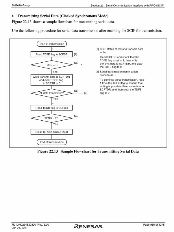
Section 22 Serial Communication Interface with FIFO (SCIF)
R01UH0234EJ0300 Rev. 3.00 Page 985 of 1278 Jun 21, 2011
SH7670 Group
• Transmitting Serial Data (Clocked Synchronous Mode)
Figure 22.13 shows a sample flowchart for transmitting serial data.
Use the following procedure for serial data transmission after enabling the SCIF for transmission.
Start of transmission
Read TDFE flag in SCFSR
TDFE = 1?
Write transmit data to SCFTDR and clear TDFE flag
in SCFSR to 0
All data transmitted?
Read TEND flag in SCFSR
TEND = 1?
Clear TE bit in SCSCR to 0
End of transmission
No
Yes
No
Yes
No
Yes
[1] SCIF status check and transmit data write:
Read SCFSR and check that the TDFE flag is set to 1, then write transmit data to SCFTDR, and clear the TDFE flag to 0.
[2] Serial transmission continuation procedeure:
To continue serial transmission, read 1 from the TDFE flag to confirm that writing is possible, them write data to SCFTDR, and then clear the TDFE flag to 0.
[1]
[2]
Figure 22.13 Sample Flowchart for Transmitting Serial Data

Section 22 Serial Communication Interface with FIFO (SCIF)
Page 986 of 1278 R01UH0234EJ0300 Rev. 3.00 Jun 21, 2011
SH7670 Group
In serial transmission, the SCIF operates as described below.
1. When data is written into the transmit FIFO data register (SCFTDR), the SCIF transfers the data from SCFTDR to the transmit shift register (SCTSR) and starts transmitting. Confirm that the TDFE flag in the serial status register (SCFSR) is set to 1 before writing transmit data to SCFTDR. The number of data bytes that can be written is (16 – transmit trigger setting).
2. When data is transferred from SCFTDR to SCTSR and transmission is started, consecutive transmit operations are performed until there is no transmit data left in SCFTDR. When the number of transmit data bytes in SCFTDR falls below the transmit trigger number set in the FIFO control register (SCFCR), the TDFE flag is set. If the TIE bit in the serial control register (SCSR) is set to 1 at this time, a transmit-FIFO-data-empty interrupt (TXI) request is generated.
If clock output mode is selected, the SCIF outputs eight synchronous clock pulses. If an external clock source is selected, the SCIF outputs data in synchronization with the input clock. Data is output from the TxD pin in order from the LSB (bit 0) to the MSB (bit 7).
3. The SCIF checks the SCFTDR transmit data at the timing for sending the MSB (bit 7). If data is present, the data is transferred from SCFTDR to SCTSR, and then serial transmission of the next frame is started. If there is no data, the TxD pin holds the state after the TEND flag in SCFSR is set to 1 and the MSB (bit 7) is sent.
4. After the end of serial transmission, the SCK pin is held in the high state. Figure 22.14 shows an example of SCIF transmit operation.
Serial clock
Serial data
TDFE
TEND
Data written to SCFTDR and TDFE flag cleared
to 0 by TXI interrupt handler
One frame
Bit 0
LSB
TXIinterruptrequest
MSB
Bit 1 Bit 6 Bit 7Bit 7 Bit 0 Bit 1
TXI interruptrequest
Figure 22.14 Example of SCIF Transmit Operation

Section 22 Serial Communication Interface with FIFO (SCIF)
R01UH0234EJ0300 Rev. 3.00 Page 987 of 1278 Jun 21, 2011
SH7670 Group
• Receiving Serial Data (Clocked Synchronous Mode)
Figures 22.15 and 22.16 show sample flowcharts for receiving serial data. When switching from asynchronous mode to clocked synchronous mode without SCIF initialization, make sure that ORER, PER, and FER are cleared to 0.
Start of reception
Read ORER flag in SCLSR
ORER = 1?
Read RDF flag in SCFSR
RDF = 1?
Read receive data inSCFRDR, and clear RDF
flag in SCFSR to 0
All data received?
Clear RE bit in SCSCR to 0
End of reception
Yes
No
Yes
Yes
No
No
Error handling
[1] Receive error handling: Read the ORER flag in SCLSR to identify any error, perform the appropriate error handling, then clear the ORER flag to 0. Reception cannot be resumed while the ORER flag is set to 1.
[2] SCIF status check and receive data read: Read SCFSR and check that RDF = 1, then read the receive data in SCFRDR, and clear the RDF flag to 0. The transition of the RDF flag from 0 to 1 can also be identified by a receive FIFO data full interrupt (RXI).
[3] Serial reception continuation procedure: To continue serial reception, read at least the receive trigger set number of receive data bytes from SCFRDR, read 1 from the RDF flag, then clear the RDF flag to 0. The number of receive data bytes in SCFRDR can be ascertained by reading SCFRDR. However, the RDF bit is cleared to 0 automatically when an RXI interrupt activates the DMAC to read the data in SCFRDR.
[1]
[2]
[3]
Figure 22.15 Sample Flowchart for Receiving Serial Data (1)

Section 22 Serial Communication Interface with FIFO (SCIF)
Page 988 of 1278 R01UH0234EJ0300 Rev. 3.00 Jun 21, 2011
SH7670 Group
Error handling
Clear ORER flag in SCLSR to 0
End
Overrun error handling
ORER = 1?
Yes
No
Figure 22.16 Sample Flowchart for Receiving Serial Data (2)
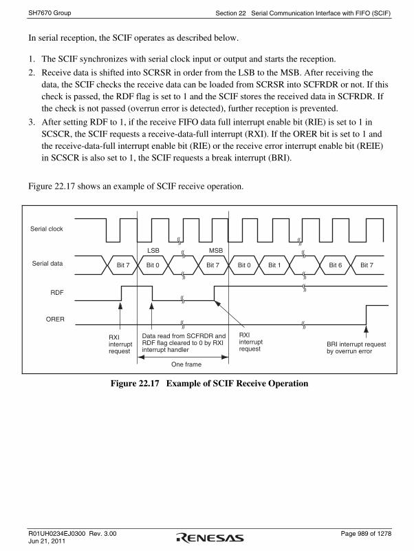
Section 22 Serial Communication Interface with FIFO (SCIF)
R01UH0234EJ0300 Rev. 3.00 Page 989 of 1278 Jun 21, 2011
SH7670 Group
In serial reception, the SCIF operates as described below.
1. The SCIF synchronizes with serial clock input or output and starts the reception.
2. Receive data is shifted into SCRSR in order from the LSB to the MSB. After receiving the data, the SCIF checks the receive data can be loaded from SCRSR into SCFRDR or not. If this check is passed, the RDF flag is set to 1 and the SCIF stores the received data in SCFRDR. If the check is not passed (overrun error is detected), further reception is prevented.
3. After setting RDF to 1, if the receive FIFO data full interrupt enable bit (RIE) is set to 1 in SCSCR, the SCIF requests a receive-data-full interrupt (RXI). If the ORER bit is set to 1 and the receive-data-full interrupt enable bit (RIE) or the receive error interrupt enable bit (REIE) in SCSCR is also set to 1, the SCIF requests a break interrupt (BRI).
Figure 22.17 shows an example of SCIF receive operation.
Bit 7 Bit 0
LSB MSB
Bit 7 Bit 0 Bit 1 Bit 6 Bit 7
RDF
ORER
Serial clock
Serial data
Data read from SCFRDR and RDF flag cleared to 0 by RXI interrupt handler
One frame
RXI interrupt request
BRI interrupt request by overrun error
RXI interrupt request
Figure 22.17 Example of SCIF Receive Operation

Section 22 Serial Communication Interface with FIFO (SCIF)
Page 990 of 1278 R01UH0234EJ0300 Rev. 3.00 Jun 21, 2011
SH7670 Group
• Transmitting and Receiving Serial Data Simultaneously (Clocked Synchronous Mode)
Figure 22.18 shows a sample flowchart for transmitting and receiving serial data simultaneously.
Use the following procedure for the simultaneous transmission/reception of serial data, after enabling the SCIF for transmission/reception.
Start of transmission and reception
Initialization
Read TDFE flag in SCFSR
TDFE = 1?
Write transmit data to SCFTDR, and clear TDFE flag
in SCFSR to 0
Read ORER flag in SCLSR
ORER = 1?
Read RDF flag in SCFSR
RDF = 1?
Clear TE and RE bits in SCSCR to 0
End of transmission and reception
Read receive data inSCFRDR, and clear RDF
flag in SCFSR to 0
All data received?
No
No
Yes
No
No
Yes
Yes
[1] SCIF status check and transmit data write:
Read SCFSR and check that the TDFE flag is set to 1, then write transmit data to SCFTDR, and clear the TDFE flag to 0. The transition of the TDFE flag from 0 to 1 can also be identified by a transmit FIFO data empty interrupt (TXI).
[2] Receive error handling:
Read the ORER flag in SCLSR to identify any error, perform the appropriate error handling, then clear the ORER flag to 0. Reception cannot be resumed while the ORER flag is set to 1.
[3] SCIF status check and receive data read:
Read SCFSR and check that RDF flag = 1, then read the receive data in SCFRDR, and clear the RDF flag to 0. The transition of the RDF flag from 0 to 1 can also be identified by a receive FIFO data full interrupt (RXI).
[4] Serial transmission and reception continuation procedure:
To continue serial transmission and reception, read 1 from the RDF flag and the receive data in SCFRDR, and clear the RDF flag to 0 before receiving the MSB in the current frame. Similarly, read 1 from the TDFE flag to confirm that writing is possible before transmitting the MSB in the current frame. Then write data to SCFTDR and clear the TDFE flag to 0.
[1]
Yes
Error handling
[4]When switching from a transmit operation or receive operation to simultaneous transmission and reception operations, clear the TE and RE bits to 0, and then set them simultaneously to 1.
Note:
[3]
[2]
Figure 22.18 Sample Flowchart for Transmitting/Receiving Serial Data

Section 22 Serial Communication Interface with FIFO (SCIF)
R01UH0234EJ0300 Rev. 3.00 Page 991 of 1278 Jun 21, 2011
SH7670 Group
22.5 SCIF Interrupts
The SCIF has four interrupt sources: transmit-FIFO-data-empty (TXI), receive-error (ERI), receive FIFO data full (RXI), and break (BRI).
Table 22.12 shows the interrupt sources and their order of priority. The interrupt sources are enabled or disabled by means of the TIE, RIE, and REIE bits in SCSCR. A separate interrupt request is sent to the interrupt controller for each of these interrupt sources.
When a TXI request is enabled by the TIE bit and the TDFE flag in the serial status register (SCFSR) is set to 1, a TXI interrupt request is generated. The DMAC can be activated and data transfer performed by this TXI interrupt request. At this time, an interrupt request is not sent to the CPU.
When an RXI request is enabled by the RIE bit and the RDF flag or the DR flag in SCFSR is set to 1, an RXI interrupt request is generated. The DMAC can be activated and data transfer performed by this RXI interrupt request. At this time, an interrupt request is not sent to the CPU. The RXI interrupt request caused by the DR flag is generated only in asynchronous mode.
When the RIE bit is set to 0 and the REIE bit is set to 1, the SCIF requests only an ERI interrupt without requesting an RXI interrupt.
The TXI indicates that transmit data can be written, and the RXI indicates that there is receive data in SCFRDR.
Table 22.12 SCIF Interrupt Sources
Interrupt Source
Description
DMAC Activation
Priority on Reset Release
BRI Interrupt initiated by break (BRK) or overrun error (ORER)
Not possible High
ERI Interrupt initiated by receive error (ER) Not possible
RXI Interrupt initiated by receive FIFO data full (RDF) or data ready (DR)
Possible
TXI Interrupt initiated by transmit FIFO data empty (TDFE)
Possible Low

Section 22 Serial Communication Interface with FIFO (SCIF)
Page 992 of 1278 R01UH0234EJ0300 Rev. 3.00 Jun 21, 2011
SH7670 Group
22.6 Usage Notes
Note the following when using the SCIF.
22.6.1 SCFTDR Writing and TDFE Flag
The TDFE flag in the serial status register (SCFSR) is set when the number of transmit data bytes written in the transmit FIFO data register (SCFTDR) has fallen below the transmit trigger number set by bits TTRG[1:0] in the FIFO control register (SCFCR). After the TDFE flag is set, transmit data up to the number of empty bytes in SCFTDR can be written, allowing efficient continuous transmission.
However, if the number of data bytes written in SCFTDR is equal to or less than the transmit trigger number, the TDFE flag will be set to 1 again after being read as 1 and cleared to 0. TDFE flag clearing should therefore be carried out when SCFTDR contains more than the transmit trigger number of transmit data bytes.
The number of transmit data bytes in SCFTDR can be found from the upper 8 bits of the FIFO data count register (SCFDR).
22.6.2 SCFRDR Reading and RDF Flag
The RDF flag in the serial status register (SCFSR) is set when the number of receive data bytes in the receive FIFO data register (SCFRDR) has become equal to or greater than the receive trigger number set by bits RTRG[1:0] in the FIFO control register (SCFCR). After RDF flag is set, receive data equivalent to the trigger number can be read from SCFRDR, allowing efficient continuous reception.
However, if the number of data bytes in SCFRDR exceeds the trigger number, the RDF flag will be set to 1 again if it is cleared to 0. The RDF flag should therefore be cleared to 0 after being read as 1 after reading the number of the received data in the receive FIFO data register (SCFRDR) which is less than the trigger number.
The number of receive data bytes in SCFRDR can be found from the lower 8 bits of the FIFO data count register (SCFDR).

Section 22 Serial Communication Interface with FIFO (SCIF)
R01UH0234EJ0300 Rev. 3.00 Page 993 of 1278 Jun 21, 2011
SH7670 Group
22.6.3 Break Detection and Processing
Break signals can be detected by reading the RxD pin directly when a framing error (FER) is detected. In the break state the input from the RxD pin consists of all 0s, so the FER flag is set and the parity error flag (PER) may also be set.
Note that, although transfer of receive data to SCFRDR is halted in the break state, the SCIF receiver continues to operate.
22.6.4 Sending a Break Signal
The I/O condition and level of the TxD pin are determined by the SPB2IO and SPB2DT bits in the serial port register (SCSPTR). This feature can be used to send a break signal.
Until TE bit is set to 1 (enabling transmission) after initializing, the TxD pin does not work. During the period, mark status is performed by the SPB2DT bit. Therefore, the SPB2IO and SPB2DT bits should be set to 1 (high level output).
To send a break signal during serial transmission, clear the SPB2DT bit to 0 (designating low level), then clear the TE bit to 0 (halting transmission). When the TE bit is cleared to 0, the transmitter is initialized regardless of the current transmission state, and 0 is output from the TxD pin.
22.6.5 Receive Data Sampling Timing and Receive Margin (Asynchronous Mode)
The SCIF operates on a base clock with a frequency of 16 times the transfer rate. In reception, the SCIF synchronizes internally with the fall of the start bit, which it samples on the base clock. Receive data is latched at the rising edge of the eighth base clock pulse. The timing is shown in figure 22.19.
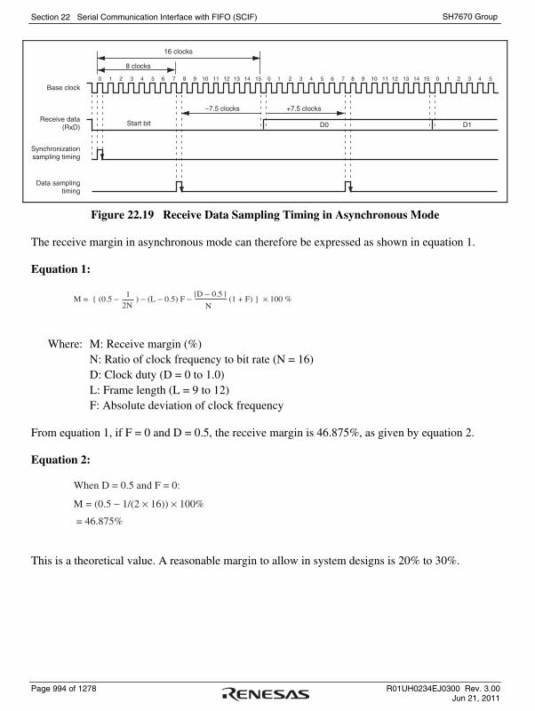
Section 22 Serial Communication Interface with FIFO (SCIF)
Page 994 of 1278 R01UH0234EJ0300 Rev. 3.00 Jun 21, 2011
SH7670 Group
D0 D1
0 1 2 3 4 5 6 7 8 9 10 11 12 13 14 15 0 1 2 3 4 5 0 1 2 3 4 56 7 8 9 10 11 12 13 14 15
16 clocks
8 clocks
Base clock
Receive data(RxD) Start bit
–7.5 clocks +7.5 clocks
Synchronizationsampling timing
Data samplingtiming
Figure 22.19 Receive Data Sampling Timing in Asynchronous Mode
The receive margin in asynchronous mode can therefore be expressed as shown in equation 1.
Equation 1:
M = { (0.5 − ) − (L − 0.5) F − (1 + F) } × 100 %1
2N
D − 0.5
N
Where: M: Receive margin (%) N: Ratio of clock frequency to bit rate (N = 16) D: Clock duty (D = 0 to 1.0) L: Frame length (L = 9 to 12) F: Absolute deviation of clock frequency
From equation 1, if F = 0 and D = 0.5, the receive margin is 46.875%, as given by equation 2.
Equation 2:
When D = 0.5 and F = 0:
M = (0.5 − 1/(2 × 16)) × 100%
= 46.875%
This is a theoretical value. A reasonable margin to allow in system designs is 20% to 30%.

Section 23 Pin Function Controller (PFC)
R01UH0234EJ0300 Rev. 3.00 Page 995 of 1278 Jun 21, 2011
SH7670 Group
Section 23 Pin Function Controller (PFC)
The pin function controller (PFC) consists of registers that select the functions of the multiplexed pins and their I/O directions. Tables 23.1 to 23.7 list the multiplexed pins of this LSI. Table 23.8 lists pin functions for each operating mode.
Table 23.1 List of Multiplexed Pins (Port A)
Port Function 1 (Related modules)
Function 2 (Related modules)
Function 3 (Related modules)
Function 4 (Related modules)
Function 5 (Related modules)
A PA25 I/O (port) A25 output (BSC) ⎯ ⎯ HIFMD input (HIF)
PA24 I/O (port) A24 output (BSC) ⎯ ⎯ ⎯
PA23 I/O (port) A23 output (BSC) ⎯ ⎯ ⎯
PA22 I/O (port) A22 output (BSC) ⎯ ⎯ ⎯
PA21 I/O (port) A21 output (BSC) ⎯ ⎯ ⎯
PA20 I/O (port) A20 output (BSC) ⎯ ⎯ ⎯
PA19 I/O (port) A19 output (BSC) ⎯ ⎯ ⎯
PA18 I/O (port) A18 output (BSC) ⎯ ⎯ ⎯
PA17 I/O (port) A17 output (BSC) ⎯ ⎯ ⎯
Table 23.2 List of Multiplexed Pins (Port B)
Port Function 1 (Related modules)
Function 2 (Related modules)
Function 3 (Related modules)
Function 4 (Related modules)
B PB07 I/O (port) BS output (BSC) ⎯ ⎯
PB06 input (port) CS4 output (BSC) ⎯ ⎯
PB05 I/O (port) CS5 output (BSC) CE1A output (BSC) IRQ3 input (INTC) TEND1 output (DMAC)
PB04 I/O (port) CE2A output (BSC) IRQ2 input (INTC) DACK1 output (DMAC)
PB03 input (port) CS6 output (BSC) CE1B output (BSC) IRQ1 input (INTC) DREQ1 input (DMAC)
PB02 input (port) CE2B output (BSC) IRQ0 input (INTC) ⎯
PB01 input (port) IOIS16 input (BSC) SCL I/O (IIC) ⎯
PB00 input (port) WAIT input (BSC) SDA I/O (IIC) ⎯
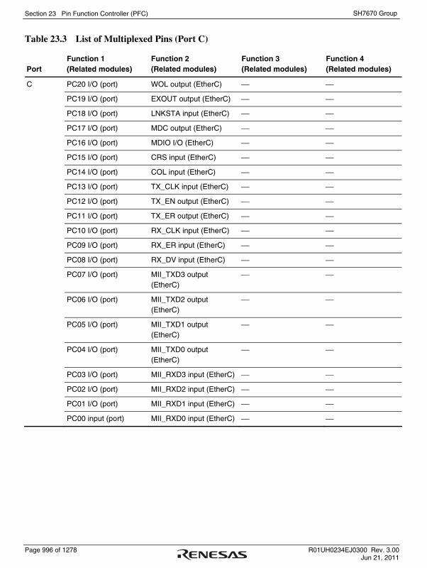
Section 23 Pin Function Controller (PFC)
Page 996 of 1278 R01UH0234EJ0300 Rev. 3.00 Jun 21, 2011
SH7670 Group
Table 23.3 List of Multiplexed Pins (Port C)
Port Function 1 (Related modules)
Function 2 (Related modules)
Function 3 (Related modules)
Function 4 (Related modules)
C PC20 I/O (port) WOL output (EtherC) ⎯ ⎯
PC19 I/O (port) EXOUT output (EtherC) ⎯ ⎯
PC18 I/O (port) LNKSTA input (EtherC) ⎯ ⎯
PC17 I/O (port) MDC output (EtherC) ⎯ ⎯
PC16 I/O (port) MDIO I/O (EtherC) ⎯ ⎯
PC15 I/O (port) CRS input (EtherC) ⎯ ⎯
PC14 I/O (port) COL input (EtherC) ⎯ ⎯
PC13 I/O (port) TX_CLK input (EtherC) ⎯ ⎯
PC12 I/O (port) TX_EN output (EtherC) ⎯ ⎯
PC11 I/O (port) TX_ER output (EtherC) ⎯ ⎯
PC10 I/O (port) RX_CLK input (EtherC) ⎯ ⎯
PC09 I/O (port) RX_ER input (EtherC) ⎯ ⎯
PC08 I/O (port) RX_DV input (EtherC) ⎯ ⎯
PC07 I/O (port) MII_TXD3 output (EtherC)
⎯ ⎯
PC06 I/O (port) MII_TXD2 output (EtherC)
⎯ ⎯
PC05 I/O (port) MII_TXD1 output (EtherC)
⎯ ⎯
PC04 I/O (port) MII_TXD0 output (EtherC)
⎯ ⎯
PC03 I/O (port) MII_RXD3 input (EtherC) ⎯ ⎯
PC02 I/O (port) MII_RXD2 input (EtherC) ⎯ ⎯
PC01 I/O (port) MII_RXD1 input (EtherC) ⎯ ⎯
PC00 input (port) MII_RXD0 input (EtherC) ⎯ ⎯

Section 23 Pin Function Controller (PFC)
R01UH0234EJ0300 Rev. 3.00 Page 997 of 1278 Jun 21, 2011
SH7670 Group
Table 23.4 List of Multiplexed Pins (Port D)
Port Function 1 (Related modules)
Function 2 (Related modules)
Function 3 (Related modules)
Function 4 (Related modules)
D PD07 I/O (port) IRQ7 input (INTC) SDCLK output (SDHI) ⎯
PD06 I/O (port) IRQ6 input (INTC) SDCMD I/O (SDHI) ⎯
PD05 input (port) IRQ5 input (INTC) SDCD input (SDHI) ⎯
PD04 input (port) IRQ4 input (INTC) SDWP input (SDHI) ⎯
PD03 I/O (port) IRQ3 input (INTC) SDDAT3 I/O (SDHI) ⎯
PD02 I/O (port) IRQ2 input (INTC) SDDAT2 I/O (SDHI) ⎯
PD01 I/O (port) IRQ1 input (INTC) SDDAT1 I/O (SDHI) ⎯
PD00 I/O (port) IRQ0 input (INTC) SDDAT0 I/O (SDHI) ⎯
Table 23.5 List of Multiplexed Pins (Port E)
Port Function 1 (Related modules)
Function 2 (Related modules)
Function 3 (Related modules)
Function 4 (Related modules)
E ⎯ ST1_CLKIN input (STIF) SSISCK1 I/O (SSI) ⎯
⎯ ST1_VCO_CLKIN input (STIF)
AUDIO_CLK input (SSI) ⎯
PE11 I/O (port) ST1_PWM output (STIF) RTS2 I/O (SCIF) ⎯
PE10 I/O (port) ST1_SYC I/O (STIF) CTS2 I/O (SCIF) ⎯
PE09 I/O (port) ST1_VLD I/O (STIF) SCK2 I/O (SCIF) ⎯
PE08 I/O (port) ST1_REQ I/O (STIF) TxD2 output (SCIF) ⎯
PE07 I/O (port) ST1_D7 I/O (STIF) SSIWS1 I/O (SSI) ⎯
PE06 I/O (port) ST1_D6 I/O (STIF) SSIDATA1 I/O (SSI) ⎯
PE05 I/O (port) ST1_D5 I/O (STIF) RTS1 I/O (SCIF) ⎯
PE04 I/O (port) ST1_D4 I/O (STIF) CTS1 I/O (SCIF) ⎯
PE03 I/O (port) ST1_D3 I/O (STIF) SCK1 I/O (SCIF) ⎯
PE02 I/O (port) ST1_D2 I/O (STIF) RxD1 input (SCIF) ⎯
PE01 I/O (port) ST1_D1 I/O (STIF) TxD1 output (SCIF) ⎯
PE00 I/O (port) ST1_D0 I/O (STIF) RxD2 input (SCIF) ⎯

Section 23 Pin Function Controller (PFC)
Page 998 of 1278 R01UH0234EJ0300 Rev. 3.00 Jun 21, 2011
SH7670 Group
Table 23.6 List of Multiplexed Pins (Port F)
Port Function 1 (Related modules)
Function 2 (Related modules)
Function 3 (Related modules)
Function 4 (Related modules)
F ⎯ ST_CLKOUT output (STIF)
⎯ ⎯
⎯ ST0_CLKIN input (STIF) SSISCK0 I/O (SSI) ⎯
⎯ ST0_VCO_CLKIN input (STIF)
⎯ ⎯
PF11 I/O (port) ST0_PWM output (STIF) TEND0 output (DMAC) ⎯
PF10 I/O (port) ST0_SYC I/O (STIF) DACK0 output (DMAC) ⎯
PF09 I/O (port) ST0_VLD I/O (STIF) DREQ0 input (DMAC) ⎯
PF08 I/O (port) ST0_REQ I/O (STIF) ⎯ ⎯
PF07 I/O (port) ST0_D7 I/O (STIF) SSIWS0 I/O (SSI) ⎯
PF06 I/O (port) ST0_D6 I/O (STIF) SSIDATA0 I/O (SSI) ⎯
PF05 I/O (port) ST0_D5 I/O (STIF) RTS0 I/O (SCIF) ⎯
PF04 I/O (port) ST0_D4 I/O (STIF) CTS0 I/O (SCIF) ⎯
PF03 I/O (port) ST0_D3 I/O (STIF) SCK0 I/O (SCIF) ⎯
PF02 I/O (port) ST0_D2 I/O (STIF) RxD0 input (SCIF) ⎯
PF01 I/O (port) ST0_D1 I/O (STIF) TxD0 output (SCIF) ⎯
PF00 I/O (port) ST0_D0 I/O (STIF) ⎯ ⎯

Section 23 Pin Function Controller (PFC)
R01UH0234EJ0300 Rev. 3.00 Page 999 of 1278 Jun 21, 2011
SH7670 Group
Table 23.7 List of Multiplexed Pins (Port G)
Port Function 1 (Related modules)
Function 2 (Related modules)
Function 3 (Related modules)
Function 4 (Related modules)
G PG23 I/O (port) HIFCS input (HIF) ⎯ ⎯
PG22 I/O (port) HIFRS input (HIF) ⎯ ⎯
PG21 I/O (port) HIFWR input (HIF) ⎯ ⎯
PG20 I/O (port) HIFRD input (HIF) ⎯ ⎯
PG19 I/O (port) HIFINT output (HIF) ⎯ ⎯
PG18 I/O (port) HIFDREQ output (HIF) ⎯ ⎯
PG17 I/O (port) HIFRDY output (HIF) ⎯ ⎯
PG16 I/O (port) HIFEBL input (HIF) ⎯ ⎯
PG15 I/O (port) HIFD15 I/O (HIF) ⎯ ⎯
PG14 I/O (port) HIFD14 I/O (HIF) ⎯ ⎯
PG13 I/O (port) HIFD13 I/O (HIF) ⎯ ⎯
PG12 I/O (port) HIFD12 I/O (HIF) ⎯ ⎯
PG11 I/O (port) HIFD11 I/O (HIF) ⎯ ⎯
PG10 I/O (port) HIFD10 I/O (HIF) ⎯ ⎯
PG09 I/O (port) HIFD09 I/O (HIF) ⎯ ⎯
PG08 I/O (port) HIFD08 I/O (HIF) ⎯ ⎯
PG07 I/O (port) HIFD07 I/O (HIF) ⎯ ⎯
PG06 I/O (port) HIFD06 I/O (HIF) ⎯ ⎯
PG05 I/O (port) HIFD05 I/O (HIF) ⎯ ⎯
PG04 I/O (port) HIFD04 I/O (HIF) ⎯ ⎯
PG03 I/O (port) HIFD03 I/O (HIF) ⎯ ⎯
PG02 I/O (port) HIFD02 I/O (HIF) ⎯ ⎯
PG01 I/O (port) HIFD01 I/O (HIF) ⎯ ⎯
PG00 I/O (port) HIFD00 I/O (HIF) ⎯ ⎯

Section 23 Pin Function Controller (PFC)
Page 1000 of 1278 R01UH0234EJ0300 Rev. 3.00 Jun 21, 2011
SH7670 Group
Table 23.8 List of Pins for Each Operating Mode (1)
Non-HIF Boot Mode HIF Boot Mode Pin No. Initial Function Settable Function Initial Function Settable Function
A2 A00 ⎯ A00 ⎯
A17 A01 ⎯ A01 ⎯
B17 A02 ⎯ A02 ⎯
C17 A03 ⎯ A03 ⎯
A16 A04 ⎯ A04 ⎯
B16 A05 ⎯ A05 ⎯
C16 A06 ⎯ A06 ⎯
A15 A07 ⎯ A07 ⎯
B15 A08 ⎯ A08 ⎯
C15 A09 ⎯ A09 ⎯
A14 A10 ⎯ A10 ⎯
B14 A11 ⎯ A11 ⎯
C14 A12 ⎯ A12 ⎯
A13 A13 ⎯ A13 ⎯
B13 A14 ⎯ A14 ⎯
C13 A15 ⎯ A15 ⎯
A12 A16 ⎯ A16 ⎯
A1 PA17 PA17/A17 PA17 PA17/A17
B2 PA18 PA18/A18 PA18 PA18/A18
B1 PA19 PA19/A19 PA19 PA19/A19
C3 PA20 PA20/A20 PA20 PA20/A20
C2 PA21 PA21/A21 PA21 PA21/A21
C1 PA22 PA22/A22 PA22 PA22/A22
D3 PA23 PA23/A23 PA23 PA23/A23
D2 PA24 PA24/A24 PA24 PA24/A24
D1 HIFMD/PA25* PA25/A25 HIFMD/PA25* PA25/A25
B12 D00 ⎯ D00 ⎯
C12 D01 ⎯ D01 ⎯
A11 D02 ⎯ D02 ⎯
B11 D03 ⎯ D03 ⎯

Section 23 Pin Function Controller (PFC)
R01UH0234EJ0300 Rev. 3.00 Page 1001 of 1278 Jun 21, 2011
SH7670 Group
Non-HIF Boot Mode HIF Boot Mode Pin No. Initial Function Settable Function Initial Function Settable Function
C11 D04 ⎯ D04 ⎯
A10 D05 ⎯ D05 ⎯
B10 D06 ⎯ D06 ⎯
C10 D07 ⎯ D07 ⎯
B7 D08 ⎯ D08 ⎯

Section 23 Pin Function Controller (PFC)
Page 1002 of 1278 R01UH0234EJ0300 Rev. 3.00 Jun 21, 2011
SH7670 Group
Table 23.8 List of Pins for Each Operating Mode (2)
Non-HIF Boot Mode HIF Boot Mode Pin No. Initial Function Settable Function Initial Function Settable Function
A7 D09 ⎯ D09 ⎯
B8 D10 ⎯ D10 ⎯
C8 D11 ⎯ D11 ⎯
A8 D12 ⎯ D12 ⎯
C9 D13 ⎯ D13 ⎯
B9 D14 ⎯ D14 ⎯
A9 D15 ⎯ D15 ⎯
K20 D16 ⎯ D16 ⎯
K19 D17 ⎯ D17 ⎯
J20 D18 ⎯ D18 ⎯
J19 D19 ⎯ D19 ⎯
H20 D20 ⎯ D20 ⎯
H19 D21 ⎯ D21 ⎯
G20 D22 ⎯ D22 ⎯
G19 D23 ⎯ D23 ⎯
E18 D24 ⎯ D24 ⎯
D20 D25 ⎯ D25 ⎯
E19 D26 ⎯ D26 ⎯
F18 D27 ⎯ D27 ⎯
E20 D28 ⎯ D28 ⎯
F19 D29 ⎯ D29 ⎯
F20 D30 ⎯ D30 ⎯
G18 D31 ⎯ D31 ⎯
A4 PB00 PB00/WAIT/SDA PB00 PB00/WAIT/SDA
C5 PB01 PB01/IOIS16/SCL PB01 PB01/IOIS16/SCL
B20 CKE ⎯ CKE ⎯
A19 CAS ⎯ CAS ⎯
A18 RAS ⎯ RAS ⎯
C7 (WE0/DQMLL) ⎯ (WE0/DQMLL) ⎯
A6 (WE1/DQMLU/WE) ⎯ (WE1/DQMLU/WE) ⎯

Section 23 Pin Function Controller (PFC)
R01UH0234EJ0300 Rev. 3.00 Page 1003 of 1278 Jun 21, 2011
SH7670 Group
Non-HIF Boot Mode HIF Boot Mode Pin No. Initial Function Settable Function Initial Function Settable Function
D19 (WE2/DQMUL/ICIORD) ⎯ (WE2/DQMUL/ICIORD) ⎯
D18 (WE3/DQMUU/ICIOWR) ⎯ (WE3/DQMUU/ICIOWR) ⎯
B5 RD ⎯ RD ⎯
C19 RDWR ⎯ RDWR ⎯
B4 PB02 PB02/CE2B/IRQ0 PB02 PB02/CE2B/IRQ0

Section 23 Pin Function Controller (PFC)
Page 1004 of 1278 R01UH0234EJ0300 Rev. 3.00 Jun 21, 2011
SH7670 Group
Table 23.8 List of Pins for Each Operating Mode (3)
Non-HIF Boot Mode HIF Boot Mode Pin No. Initial Function Settable Function Initial Function Settable Function
C4 PB03 PB03/CS6/CE1B/IRQ1/ DREQ1
PB03 PB03/CS6/CE1B/IRQ1/ DREQ1
A3 PB04 PB04/CE2A/IRQ2/DACK1 PB04 PB04/CE2A/IRQ2/DACK1
B3 PB05 PB05/CS5/CE1A/IRQ3/ TEND1
PB05 PB05/CS5/CE1A/IRQ3/ TEND1
A5 PB06 PB06/CS4 PB06 PB06/CS4
B18 CS3 ⎯ CS3 ⎯
C6 CS0 ⎯ CS0 ⎯
B6 PB07 PB07/BS PB07 PB07/BS
L1 PC00 PC00/MII_RXD0 PC00 PC00/MII_RXD0
L2 PC01 PC01/MII_RXD1 PC01 PC01/MII_RXD1
L3 PC02 PC02/MII_RXD2 PC02 PC02/MII_RXD2
K1 PC03 PC03/MII_RXD3 PC03 PC03/MII_RXD3
H1 PC04 PC04/MII_TXD0 PC04 PC04/MII_TXD0
H2 PC05 PC05/MII_TXD1 PC05 PC05/MII_TXD1
H3 PC06 PC06/MII_TXD2 PC06 PC06/MII_TXD2
G1 PC07 PC07/MII_TXD3 PC07 PC07/MII_TXD3
K2 PC08 PC08/RX_DV PC08 PC08/RX_DV
K3 PC09 PC09/RX_ER PC09 PC09/RX_ER
J1 PC10 PC10/RX_CLK PC10 PC10/RX_CLK
G2 PC11 PC11/TX_ER PC11 PC11/TX_ER
G3 PC12 PC12/TX_EN PC12 PC12/TX_EN
F1 PC13 PC13/TX_CLK PC13 PC13/TX_CLK
J2 PC14 PC14/COL PC14 PC14/COL
J3 PC15 PC15/CRS PC15 PC15/CRS
F2 PC16 PC16/MDIO PC16 PC16/MDIO
F3 PC17 PC17/MDC PC17 PC17/MDC
E1 PC18 PC18/LNKSTA PC18 PC18/LNKSTA
E2 PC19 PC19/EXOUT PC19 PC19/EXOUT
E3 PC20 PC20/WOL PC20 PC20/WOL
R3 PD00 PD00/IRQ0/SDATA0 PD00 PD00/IRQ0/SDATA0

Section 23 Pin Function Controller (PFC)
R01UH0234EJ0300 Rev. 3.00 Page 1005 of 1278 Jun 21, 2011
SH7670 Group
Non-HIF Boot Mode HIF Boot Mode Pin No. Initial Function Settable Function Initial Function Settable Function
P1 PD01 PD01/IRQ1/SDATA1 PD01 PD01/IRQ1/SDATA1
P2 PD02 PD02/IRQ2/SDATA2 PD02 PD02/IRQ2/SDATA2
P3 PD03 PD03/IRQ3/SDATA3 PD03 PD03/IRQ3/SDATA3

Section 23 Pin Function Controller (PFC)
Page 1006 of 1278 R01UH0234EJ0300 Rev. 3.00 Jun 21, 2011
SH7670 Group
Table 23.8 List of Pins for Each Operating Mode (4)
Non-HIF Boot Mode HIF Boot Mode Pin No. Initial Function Settable Function Initial Function Settable Function
N1 PD04 PD04/IRQ4/SDWP PD04 PD04/IRQ4/SDWP
N2 PD05 PD05/IRQ5/SDCD PD05 PD05/IRQ5/SDCD
N3 PD06 PD06/IRQ6/SDCMD PD06 PD06/IRQ6/SDCMD
M3 PD07 PD07/IRQ7/SDCLK PD07 PD07/IRQ7/SDCLK
Y15 PE00 PE00/ST1_D0/RxD2 PE00 PE00/ST1_D0/RxD2
V14 PE01 PE01/ST1_D1/TxD1 PE01 PE01/ST1_D1/TxD1
W14 PE02 PE02/ST1_D2/RxD1 PE02 PE02/ST1_D2/RxD1
V15 PE03 PE03/ST1_D3/SCK1 PE03 PE03/ST1_D3/SCK1
Y13 PE04 PE04/ST1_D4/CTS1 PE04 PE04/ST1_D4/CTS1
W13 PE05 PE05/ST1_D5/RTS1 PE05 PE05/ST1_D5/RTS1
V13 PE06 PE06/ST1_D6/SSIDATA1 PE06 PE06/ST1_D6/SSIDATA1
V12 PE07 PE07/ST1_D7/SSIWS1 PE07 PE07/ST1_D7/SSIWS1
Y16 PE08 PE08/ST1_REQ/TxD2 PE08 PE08/ST1_REQ/TxD2
Y14 PE09 PE09/ST1_VLD/SCK2 PE09 PE09/ST1_VLD/SCK2
W15 PE10 PE10/ST1_SYC/CTS2 PE10 PE10/ST1_SYC/CTS2
W16 ST1_PWM PE11/ST1_PWM/RTS2 ST1_PWM PE11/ST1_PWM/RTS2
V16 ⎯ ST1_VCO_CLKIN/ AUDIO_CLK
⎯ ST1_VCO_CLKIN/ AUDIO_CLK
W17 ⎯ ST1_CLKIN/SSISCK1 ⎯ ST1_CLKIN/SSISCK1
N20 PF00 PF00/ST0_D0 PF00 PF00/ST0_D0
N18 PF01 PF01/ST0_D1/TxD0 PF01 PF01/ST0_D1/TxD0
M18 PF02 PF02/ST0_D2/RxD0 PF02 PF02/ST0_D2/RxD0
M19 PF03 PF03/ST0_D3/SCK0 PF03 PF03/ST0_D3/SCK0
M20 PF04 PF04/ST0_D4/CTS0 PF04 PF04/ST0_D4/CTS0
L18 PF05 PF05/ST0_D5/RTS0 PF05 PF05/ST0_D5/RTS0
L19 PF06 PF06/ST0_D6/SSIDATA0 PF06 PF06/ST0_D6/SSIDATA0
L20 PF07 PF07/ST0_D7/SSIWS0 PF07 PF07/ST0_D7/SSIWS0
P19 PF08 PF08/ST0_REQ PF08 PF08/ST0_REQ
P20 PF09 PF09/ST0_VLD/DREQ0 PF09 PF09/ST0_VLD/DREQ0
N19 PF10 PF10/ST0_SYC/DACK0 PF10 PF10/ST0_SYC/DACK0
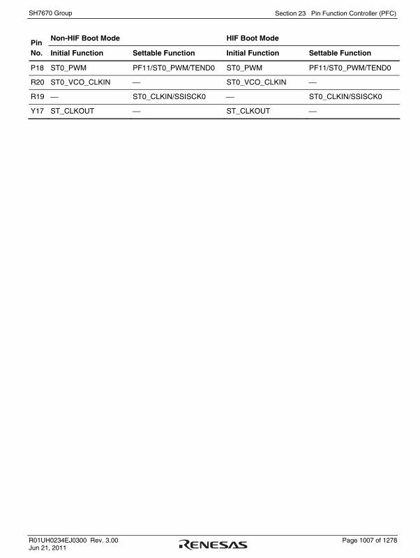
Section 23 Pin Function Controller (PFC)
R01UH0234EJ0300 Rev. 3.00 Page 1007 of 1278 Jun 21, 2011
SH7670 Group
Non-HIF Boot Mode HIF Boot Mode Pin No. Initial Function Settable Function Initial Function Settable Function
P18 ST0_PWM PF11/ST0_PWM/TEND0 ST0_PWM PF11/ST0_PWM/TEND0
R20 ST0_VCO_CLKIN ⎯ ST0_VCO_CLKIN ⎯
R19 ⎯ ST0_CLKIN/SSISCK0 ⎯ ST0_CLKIN/SSISCK0
Y17 ST_CLKOUT ⎯ ST_CLKOUT ⎯

Section 23 Pin Function Controller (PFC)
Page 1008 of 1278 R01UH0234EJ0300 Rev. 3.00 Jun 21, 2011
SH7670 Group
Table 23.8 List of Pins for Each Operating Mode (5)
Non-HIF Boot Mode HIF Boot Mode Pin No. Initial Function Settable Function Initial Function Settable Function
W4 PG00 PG00/HIFD00 HIFD00 PG00/HIFD00
V4 PG01 PG01/HIFD01 HIFD01 PG01/HIFD01
Y3 PG02 PG02/HIFD02 HIFD02 PG02/HIFD02
W3 PG03 PG03/HIFD03 HIFD03 PG03/HIFD03
V3 PG04 PG04/HIFD04 HIFD04 PG04/HIFD04
Y2 PG05 PG05/HIFD05 HIFD05 PG05/HIFD05
W2 PG06 PG06/HIFD06 HIFD06 PG06/HIFD06
V1 PG07 PG07/HIFD07 HIFD07 PG07/HIFD07
Y1 PG08 PG08/HIFD08 HIFD08 PG08/HIFD08
U1 PG09 PG09/HIFD09 HIFD09 PG09/HIFD09
U2 PG10 PG10/HIFD10 HIFD10 PG10/HIFD10
T1 PG11 PG11/HIFD11 HIFD11 PG11/HIFD11
T2 PG12 PG12/HIFD12 HIFD12 PG12/HIFD12
T3 PG13 PG13/HIFD13 HIFD13 PG13/HIFD13
R1 PG14 PG14/HIFD14 HIFD14 PG14/HIFD14
R2 PG15 PG15/HIFD15 HIFD15 PG15/HIFD15
W7 PG16 PG16/HIFEBL HIFEBL PG16/HIFEBL
V6 PG17 PG17/HIFRDY HIFRDY PG17/HIFRDY
W6 PG18 PG18/HIFDREQ HIFDREQ PG18/HIFDREQ
Y6 PG19 PG19/HIFINT HIFINT PG19/HIFINT
Y5 PG20 PG20/HIFRD HIFRD PG20/HIFRD
W5 PG21 PG21/HIFWR HIFWR PG21/HIFWR
V5 PG22 PG22/HIFRS HIFRS PG22/HIFRS
Y4 PG23 PG23/HIFCS HIFCS PG23/HIFCS
Y9 DP ⎯ DP ⎯
Y8 DM ⎯ DM ⎯
W9 VBUS ⎯ VBUS ⎯
Y11 REFRIN ⎯ REFRIN ⎯
W12 USB_X1 ⎯ USB_X1 ⎯
Y12 USB_X2 ⎯ USB_X2 ⎯
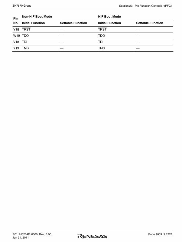
Section 23 Pin Function Controller (PFC)
R01UH0234EJ0300 Rev. 3.00 Page 1009 of 1278 Jun 21, 2011
SH7670 Group
Non-HIF Boot Mode HIF Boot Mode Pin No. Initial Function Settable Function Initial Function Settable Function
Y18 TRST ⎯ TRST ⎯
W19 TDO ⎯ TDO ⎯
V18 TDI ⎯ TDI ⎯
Y19 TMS ⎯ TMS ⎯

Section 23 Pin Function Controller (PFC)
Page 1010 of 1278 R01UH0234EJ0300 Rev. 3.00 Jun 21, 2011
SH7670 Group
Table 23.8 List of Pins for Each Operating Mode (6)
Non-HIF Boot Mode HIF Boot Mode Pin No. Initial Function Settable Function Initial Function Settable Function
V17 TCK ⎯ TCK ⎯
T20 ASEBRK/ASEBRKAK ⎯ ASEBRK/ASEBRKAK ⎯
U8 DG12 ⎯ DG12 ⎯
U9 DV12 ⎯ DV12 ⎯
U10 UV12 ⎯ UV12 ⎯
U11 AV12 ⎯ AV12 ⎯
V10 UG12 ⎯ UG12 ⎯
V11 AG12 ⎯ AG12 ⎯
W8 DG33 ⎯ DG33 ⎯
W10 AG33 ⎯ AG33 ⎯
Y10 AV33 ⎯ AV33 ⎯
V20 EXTAL ⎯ EXTAL ⎯
W20 XTAL ⎯ XTAL ⎯
C20 CKIO ⎯ CKIO ⎯
M2 ASEMD ⎯ ASEMD ⎯
M1 TESTMD ⎯ TESTMD ⎯
T19 MD_BW ⎯ MD_BW ⎯
U18 MD_CK1 ⎯ MD_CK1 ⎯
V19 MD_CK0 ⎯ MD_CK0 ⎯
W18 RES ⎯ RES ⎯
U19 NMI ⎯ NMI ⎯
R18 WDTOVF ⎯ WDTOVF ⎯
Note: * This pin functions as HIFMD during a power-on reset that is output from the RES pin.

Section 23 Pin Function Controller (PFC)
R01UH0234EJ0300 Rev. 3.00 Page 1011 of 1278 Jun 21, 2011
SH7670 Group
23.1 Register Descriptions
The PFC has the following registers. For the address and status at each processing state of these registers, see section 28, List of Registers.
Port A I/O register H (PAIORH)
Port A control register H2 (PACRH2)
Port A control register H1 (PACRH1)
Port B I/O register L (PBIORL)
Port B control register L1 (PBCRL1)
Port C I/O register H (PCIORH)
Port C I/O register L (PCIORL)
Port C control register H1 (PCCRH1)
Port C control register L2 (PCCRL2)
Port C control register L1 (PCCRL1)
Port D I/O register L (PDIORL)
Port D control register L1 (PDCRL1)
Port E I/O register L (PEIORL)
Port E control register L2 (PECRL2)
Port E control register L1 (PECRL1)
Port F I/O register L (PFIORL)
Port F control register L2 (PFCRL2)
Port F control register L1 (PFCRL1)
Port G I/O register H (PGIORH)
Port G I/O register L (PGIORL)

Section 23 Pin Function Controller (PFC)
Page 1012 of 1278 R01UH0234EJ0300 Rev. 3.00 Jun 21, 2011
SH7670 Group
Port G control register H1 (PGCRH1)
Port G control register L1 (PGCRL1)
Port G control register L2 (PGCRL2)
23.1.1 Port A I/O Register H (PAIORH)
PAIORH is a 16-bit readable/writable register that selects the input/output direction for the port A pins. Bits PA25IOR to PA17IOR correspond to pins PA25 to PA17 (multiplexed pin names other than port names are omitted), respectively. PAIORH is enabled when the function of the port A pins is set to general-purpose I/O (PA25 to PA17), and is disabled in other cases.
When a bit in PAIORH is set to 1, the corresponding pin is set to output, and when set to 0, the pin is set to input.
Bits 15 to 10 and 0 in PAIORH are reserved. These bits are always read as 0. The write value should always be 0.
The initial value of PAIORH is H'0000.
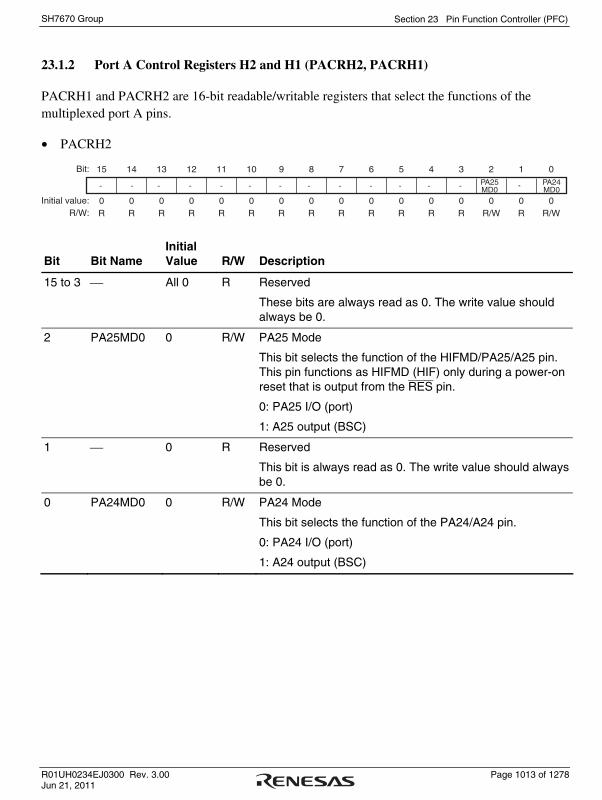
Section 23 Pin Function Controller (PFC)
R01UH0234EJ0300 Rev. 3.00 Page 1013 of 1278 Jun 21, 2011
SH7670 Group
23.1.2 Port A Control Registers H2 and H1 (PACRH2, PACRH1)
PACRH1 and PACRH2 are 16-bit readable/writable registers that select the functions of the multiplexed port A pins.
• PACRH2
15 14 13 12 11 10 9 8 7 6 5 4 3 2 1 0Bit:
Initial value:R/W:
0 0 0 0 0 0 0 0 0 0 0 0 0 0 0 0R R R R R R R R R R R R R R/W R R/W
PA25 MD0
PA24 MD0- - - - - - - -- - -- - -
Bit Bit Name Initial Value R/W Description
15 to 3 ⎯ All 0 R Reserved
These bits are always read as 0. The write value should always be 0.
2 PA25MD0 0 R/W PA25 Mode
This bit selects the function of the HIFMD/PA25/A25 pin. This pin functions as HIFMD (HIF) only during a power-on reset that is output from the RES pin.
0: PA25 I/O (port)
1: A25 output (BSC)
1 ⎯ 0 R Reserved
This bit is always read as 0. The write value should always be 0.
0 PA24MD0 0 R/W PA24 Mode
This bit selects the function of the PA24/A24 pin.
0: PA24 I/O (port)
1: A24 output (BSC)

Section 23 Pin Function Controller (PFC)
Page 1014 of 1278 R01UH0234EJ0300 Rev. 3.00 Jun 21, 2011
SH7670 Group
• PACRH1
15 14 13 12 11 10 9 8 7 6 5 4 3 2 1 0Bit:
Initial value:R/W:
0 0 0 0 0 0 0 0 0 0 0 0 0 0 0 0R R/W R R/W R R/W R R/W R R/W R R/W R R/W R R
PA23 MD0
PA22 MD0
PA21 MD0
PA20 MD0
PA19 MD0
PA18 MD0
PA17 MD0- - - - - - - - -
Bit Bit Name Initial Value R/W Description
15 ⎯ 0 R Reserved
This bit is always read as 0. The write value should always be 0.
14 PA23MD0 0 R/W PA23 Mode
This bit selects the function of the PA23/A23 pin.
0: PA23 I/O (port)
1: A23 output (BSC)
13 ⎯ 0 R Reserved
This bit is always read as 0. The write value should always be 0.
12 PA22MD0 0 R/W PA22 Mode
This bit selects the function of the PA22/A22 pin.
0: PA22 I/O (port)
1: A22 output (BSC)
11 ⎯ 0 R Reserved
This bit is always read as 0. The write value should always be 0.
10 PA21MD0 0 R/W PA21 Mode
This bit selects the function of the PA21/A21 pin.
0: PA21 I/O (port)
1: A21 output (BSC)
9 ⎯ 0 R Reserved
This bit is always read as 0. The write value should always be 0.
8 PA20MD0 0 R/W PA20 Mode
This bit selects the function of the PA20/A20 pin.
0: PA20 I/O (port)
1: A20 output (BSC)
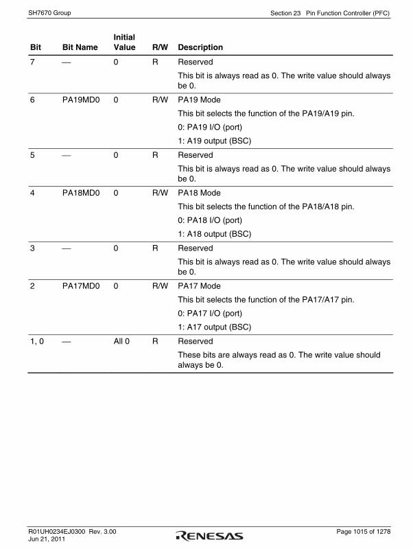
Section 23 Pin Function Controller (PFC)
R01UH0234EJ0300 Rev. 3.00 Page 1015 of 1278 Jun 21, 2011
SH7670 Group
Bit Bit Name Initial Value R/W Description
7 ⎯ 0 R Reserved
This bit is always read as 0. The write value should always be 0.
6 PA19MD0 0 R/W PA19 Mode
This bit selects the function of the PA19/A19 pin.
0: PA19 I/O (port)
1: A19 output (BSC)
5 ⎯ 0 R Reserved
This bit is always read as 0. The write value should always be 0.
4 PA18MD0 0 R/W PA18 Mode
This bit selects the function of the PA18/A18 pin.
0: PA18 I/O (port)
1: A18 output (BSC)
3 ⎯ 0 R Reserved
This bit is always read as 0. The write value should always be 0.
2 PA17MD0 0 R/W PA17 Mode
This bit selects the function of the PA17/A17 pin.
0: PA17 I/O (port)
1: A17 output (BSC)
1, 0 ⎯ All 0 R Reserved
These bits are always read as 0. The write value should always be 0.

Section 23 Pin Function Controller (PFC)
Page 1016 of 1278 R01UH0234EJ0300 Rev. 3.00 Jun 21, 2011
SH7670 Group
23.1.3 Port B I/O Register L (PBIORL)
PBIORL is a 16-bit readable/writable register that selects the input/output direction for the port B pins. Bits PB7IOR to PB0IOR correspond to pins PB07 to PB00 (multiplexed pin names other than port names are omitted), respectively. PBIORL is enabled when the function of the port B pins is set to general-purpose I/O (PB07 to PB00), and is disabled in other cases.
When a bit in PBIORL is set to 1, the corresponding pin is set to output, and when set to 0, the pin is set to input.
Bits 15 to 8 in PBIORL are reserved. These bits are always read as 0. The write value should always be 0.
The initial value of PBIORL is H'0000.

Section 23 Pin Function Controller (PFC)
R01UH0234EJ0300 Rev. 3.00 Page 1017 of 1278 Jun 21, 2011
SH7670 Group
23.1.4 Port B Control Register L1 (PBCRL1)
PBCRL1 is a 16-bit readable/writable register that selects the functions of the multiplexed port B pins.
15 14 13 12 11 10 9 8 7 6 5 4 3 2 1 0Bit:
Initial value:R/W:
0 0 0 0 0 0 0 0 0 0 0 0 0 0 0 0R R/W R R/W R/W R/W R/W R/W R/W R/W R/W R/W R/W R/W R/W R/W
PB7MD0 -- PB6
MD0PB5MD1
PB5MD0
PB4MD1
PB4MD0
PB3MD1
PB3MD0
PB2MD1
PB2MD0
PB1MD1
PB1MD0
PB0MD1
PB0MD0
Bit Bit Name Initial Value R/W Description
15 ⎯ 0 R Reserved
This bit is always read as 0. The write value should always be 0.
14 PB7MD0 0 R/W PB7 Mode
This bit selects the function of the PB07/BS pin.
0: PB07 I/O (port)
1: BS output (BSC)
13 ⎯ 0 R Reserved
This bit is always read as 0. The write value should always be 0.
12 PB6MD0 0 R/W PB6 Mode
This bit selects the function of the PB06/CS4 pin.
0: PB06 input (port)
1: CS4 output (BSC)
11
10
PB5MD1
PB5MD0
0
0
R/W
R/W
PB5 Mode
These bits select the function of the PB05/CS5/CE1A/IRQ3/TEND1 pin.
00: PB05 I/O (port)
01: CS5/CE1A output (BSC)
10: IRQ3 input (INTC)
11: TEND1 output (DMAC)

Section 23 Pin Function Controller (PFC)
Page 1018 of 1278 R01UH0234EJ0300 Rev. 3.00 Jun 21, 2011
SH7670 Group
Bit Bit Name Initial Value R/W Description
9
8
PB4MD1
PB4MD0
0
0
R/W
R/W
PB4 Mode
These bits select the function of the PB04/CE2A/IRQ2/DACK1 pin.
00: PB04 I/O (port)
01: CE2A output (BSC)
10: IRQ2 input (INTC)
11: DACK1 output (DMAC)
7
6
PB3MD1
PB3MD0
0
0
R/W
R/W
PB3 Mode
These bits select the function of the PB03/CS6/CE1B/DREQ1 pin.
00: PB03 input (port)
01: CS6/CE1B output (BSC)
10: IRQ1 input (INTC)
11: DREQ1 input (DMAC)
5
4
PB2MD1
PB2MD0
0
0
R/W
R/W
PB2 Mode
These bits select the function of the PB02/CE2B/IRQ0 pin.
00: PB02 input (port)
01: CE2B output (BSC)
10: IRQ0 input (INTC)
11: Setting prohibited
3
2
PB1MD1
PB1MD0
0
0
R/W
R/W
PB1 Mode
These bits select the function of the PB01/IOIS16/SCL pin.
00: PB01 input (port)
01: IOIS16 input (BSC)
10: SCL I/O (IIC)
11: Setting prohibited
1
0
PB0MD1
PB0MD0
0
0
R/W
R/W
PB0 Mode
These bits select the function of the PB00/WAIT/SDA pin.
00: PB00 input (port)
01: WAIT input (BSC)
10: SDA I/O (IIC)
11: Setting prohibited

Section 23 Pin Function Controller (PFC)
R01UH0234EJ0300 Rev. 3.00 Page 1019 of 1278 Jun 21, 2011
SH7670 Group
23.1.5 Port C I/O Registers H and L (PCIORH, PCIORL)
PCIORH and PCIORL are 16-bit readable/writable registers that select the input/output direction for the port C pins. Bits PC20IOR to PC0IOR correspond to pins PC20 to PC00 (multiplexed pin names other than port names are omitted), respectively. PCIORH is enabled when the function of the port C pins is set to general-purpose I/O (PC20 to PC16), and is disabled in other cases. PCIORL is enabled when the function of the port C pins is set to general-purpose I/O (PC15 to PC00), and is disabled in other cases.
When a bit in PCIORH and PCIORL is set to 1, the corresponding pin is set to output, and when set to 0, the pin is set to input.
Bits 15 to 5 in PCIORH are reserved. These bits are always read as 0. The write value should always be 0.
The initial value of PCIORH and PCIORL is H'0000.

Section 23 Pin Function Controller (PFC)
Page 1020 of 1278 R01UH0234EJ0300 Rev. 3.00 Jun 21, 2011
SH7670 Group
23.1.6 Port C Control Registers H1, L2, and L1 (PCCRH1, PCCRL2, PCCRL1)
PCCRH1, PCCRL2, and PCCRL1 are 16-bit readable/writable registers that select the functions of the multiplexed port C pins.
• PCCRH1
15 14 13 12 11 10 9 8 7 6 5 4 3 2 1 0Bit:
Initial value:R/W:
0 0 0 0 0 0 0 0 0 0 0 0 0 0 0 0R R R R R R R R/W R R/W R R/W R R/W R R/W
PC20 MD0
PC19 MD0
PC17 MD0
PC16 MD0
PC18 MD0- - - - - - - -- --
Bit Bit Name Initial Value R/W Description
15 to 9 ⎯ All 0 R Reserved
These bits are always read as 0. The write value should always be 0.
8 PC20MD0 0 R/W PC20 Mode
This bit selects the function of the PC20/WOL pin.
0: PC20 I/O (port)
1: WOL output (EtherC)
7 ⎯ 0 R Reserved
This bit is always read as 0. The write value should always be 0.
6 PC19MD0 0 R/W PC19 Mode
This bit selects the function of the PC19/EXOUT pin.
0: PC19 I/O (port)
1: EXOUT output (EtherC)
5 ⎯ 0 R Reserved
This bit is always read as 0. The write value should always be 0.
4 PC18MD0 0 R/W PC18 Mode
This bit selects the function of the PC18/LNKSTA pin.
0: PC18 I/O (port)
1: LNKSTA input (EtherC)
3 ⎯ 0 R Reserved
This bit is always read as 0. The write value should always be 0.

Section 23 Pin Function Controller (PFC)
R01UH0234EJ0300 Rev. 3.00 Page 1021 of 1278 Jun 21, 2011
SH7670 Group
Bit Bit Name Initial Value R/W Description
2 PC17MD0 0 R/W PC17 Mode
This bit selects the function of the PC17/MDC pin.
0: PC17 I/O (port)
1: MDC output (EtherC)
1 ⎯ 0 R Reserved
This bit is always read as 0. The write value should always be 0.
0 PC16MD0 0 R/W PC16 Mode
This bit selects the function of the PC16/MDIO pin.
0: PC16 I/O (port)
1: MDIO I/O (EtherC)
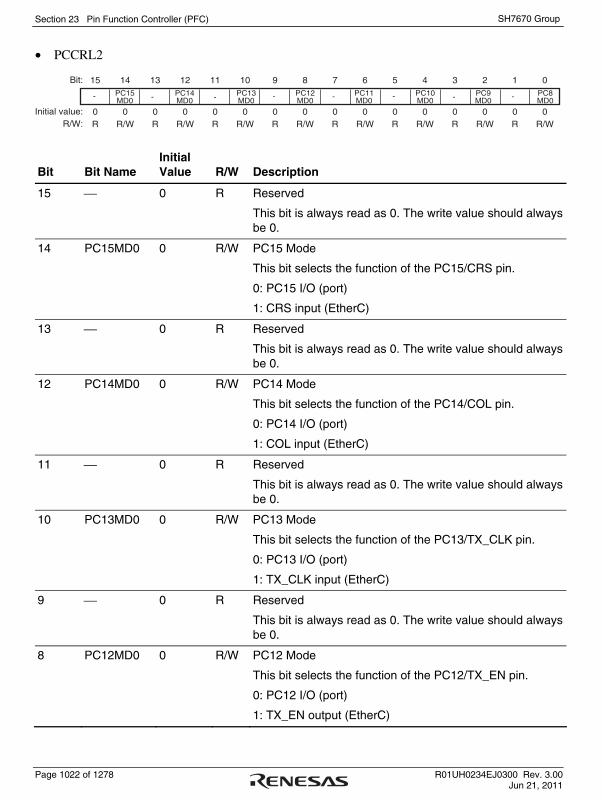
Section 23 Pin Function Controller (PFC)
Page 1022 of 1278 R01UH0234EJ0300 Rev. 3.00 Jun 21, 2011
SH7670 Group
• PCCRL2
15 14 13 12 11 10 9 8 7 6 5 4 3 2 1 0Bit:
Initial value:R/W:
0 0 0 0 0 0 0 0 0 0 0 0 0 0 0 0R R/W R R/W R R/W R R/W R R/W R R/W R R/W R R/W
PC15 MD0
PC14 MD0
PC13 MD0
PC12 MD0
PC11 MD0
PC10 MD0
PC9 MD0
PC8 MD0
- - - - - - - -
Bit Bit Name Initial Value R/W Description
15 ⎯ 0 R Reserved
This bit is always read as 0. The write value should always be 0.
14 PC15MD0 0 R/W PC15 Mode
This bit selects the function of the PC15/CRS pin.
0: PC15 I/O (port)
1: CRS input (EtherC)
13 ⎯ 0 R Reserved
This bit is always read as 0. The write value should always be 0.
12 PC14MD0 0 R/W PC14 Mode
This bit selects the function of the PC14/COL pin.
0: PC14 I/O (port)
1: COL input (EtherC)
11 ⎯ 0 R Reserved
This bit is always read as 0. The write value should always be 0.
10 PC13MD0 0 R/W PC13 Mode
This bit selects the function of the PC13/TX_CLK pin.
0: PC13 I/O (port)
1: TX_CLK input (EtherC)
9 ⎯ 0 R Reserved
This bit is always read as 0. The write value should always be 0.
8 PC12MD0 0 R/W PC12 Mode
This bit selects the function of the PC12/TX_EN pin.
0: PC12 I/O (port)
1: TX_EN output (EtherC)

Section 23 Pin Function Controller (PFC)
R01UH0234EJ0300 Rev. 3.00 Page 1023 of 1278 Jun 21, 2011
SH7670 Group
Bit Bit Name Initial Value R/W Description
7 ⎯ 0 R Reserved
This bit is always read as 0. The write value should always be 0.
6 PC11MD0 0 R/W PC11 Mode
This bit selects the function of the PC11/TX_ER pin.
0: PC11 I/O (port)
1: TX_ER output (EtherC)
5 ⎯ 0 R Reserved
This bit is always read as 0. The write value should always be 0.
4 PC10MD0 0 R/W PC10 Mode
This bit selects the function of the PC10/RX_CLK pin.
0: PC10 I/O (port)
1: RX_CLK input (EtherC)
3 ⎯ 0 R Reserved
This bit is always read as 0. The write value should always be 0.
2 PC9MD0 0 R/W PC9 Mode
This bit selects the function of the PC09/RX_ER pin.
0: PC09 I/O (port)
1: RX_ER input (EtherC)
1 ⎯ 0 R Reserved
This bit is always read as 0. The write value should always be 0.
0 PC8MD0 0 R/W PC8 Mode
This bit selects the function of the PC08/RX_DV pin.
0: PC08 I/O (port)
1: RX_DV input (EtherC)

Section 23 Pin Function Controller (PFC)
Page 1024 of 1278 R01UH0234EJ0300 Rev. 3.00 Jun 21, 2011
SH7670 Group
• PCCRL1
15 14 13 12 11 10 9 8 7 6 5 4 3 2 1 0Bit:
Initial value:R/W:
0 0 0 0 0 0 0 0 0 0 0 0 0 0 0 0R R/W R R/W R R/W R R/W R R/W R R/W R R/W R R/W
PF7MD0
PF6MD0
PF5MD0
PF4MD0
PF3MD0
PF2MD0
PF1MD0
PF0MD0- - - -- - - -
Bit Bit Name Initial Value R/W Description
15 ⎯ 0 R Reserved
This bit is always read as 0. The write value should always be 0.
14 PC7MD0 0 R/W PC7 Mode
This bit selects the function of the PC07/MII_TXD3 pin.
0: PC07 I/O (port)
1: MII_TXD3 output (EtherC)
13 ⎯ 0 R Reserved
This bit is always read as 0. The write value should always be 0.
12 PC6MD0 0 R/W PC6 Mode
This bit selects the function of the PC06/MII_TXD2 pin.
0: PC06 I/O (port)
1: MII_TXD2 output (EtherC)
11 ⎯ 0 R Reserved
This bit is always read as 0. The write value should always be 0.
10 PC5MD0 0 R/W PC5 Mode
This bit selects the function of the PC05/MII_TXD1 pin.
0: PC05 I/O (port)
1: MII_TXD1 output (EtherC)
9 ⎯ 0 R Reserved
This bit is always read as 0. The write value should always be 0.
8 PC4MD0 0 R/W PC4 Mode
This bit selects the function of the PC04/MII_TXD0 pin.
0: PC04 I/O (port)
1: MII_TXD0 output (EtherC)
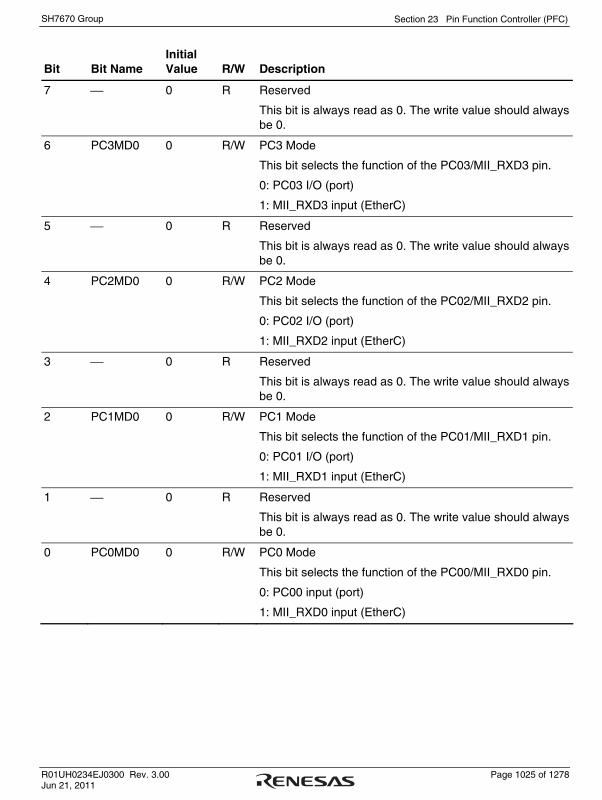
Section 23 Pin Function Controller (PFC)
R01UH0234EJ0300 Rev. 3.00 Page 1025 of 1278 Jun 21, 2011
SH7670 Group
Bit Bit Name Initial Value R/W Description
7 ⎯ 0 R Reserved
This bit is always read as 0. The write value should always be 0.
6 PC3MD0 0 R/W PC3 Mode
This bit selects the function of the PC03/MII_RXD3 pin.
0: PC03 I/O (port)
1: MII_RXD3 input (EtherC)
5 ⎯ 0 R Reserved
This bit is always read as 0. The write value should always be 0.
4 PC2MD0 0 R/W PC2 Mode
This bit selects the function of the PC02/MII_RXD2 pin.
0: PC02 I/O (port)
1: MII_RXD2 input (EtherC)
3 ⎯ 0 R Reserved
This bit is always read as 0. The write value should always be 0.
2 PC1MD0 0 R/W PC1 Mode
This bit selects the function of the PC01/MII_RXD1 pin.
0: PC01 I/O (port)
1: MII_RXD1 input (EtherC)
1 ⎯ 0 R Reserved
This bit is always read as 0. The write value should always be 0.
0 PC0MD0 0 R/W PC0 Mode
This bit selects the function of the PC00/MII_RXD0 pin.
0: PC00 input (port)
1: MII_RXD0 input (EtherC)

Section 23 Pin Function Controller (PFC)
Page 1026 of 1278 R01UH0234EJ0300 Rev. 3.00 Jun 21, 2011
SH7670 Group
23.1.7 Port D I/O Register L (PDIORL)
PDIORL is a 16-bit readable/writable register that selects the input/output direction for the port D pins. Bits PD7IOR to PD0IOR correspond to pins PD07 to PD00 (multiplexed pin names other than port names are omitted), respectively. PDIORL is enabled when the function of the port D pins is set to general-purpose I/O (PD07 to PD00), and is disabled in other cases.
When a bit in PDIORL is set to 1, the corresponding pin is set to output, and when set to 0, the pin is set to input.
Bits 15 to 8 in PDIORL are reserved. These bits are always read as 0. The write value should always be 0.
The initial value of PDIORL is H'0000.
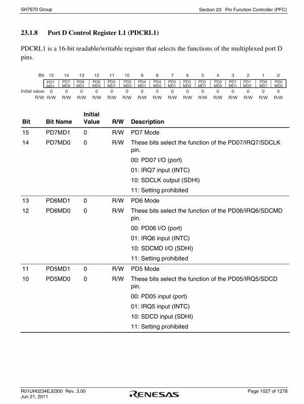
Section 23 Pin Function Controller (PFC)
R01UH0234EJ0300 Rev. 3.00 Page 1027 of 1278 Jun 21, 2011
SH7670 Group
23.1.8 Port D Control Register L1 (PDCRL1)
PDCRL1 is a 16-bit readable/writable register that selects the functions of the multiplexed port D pins.
15 14 13 12 11 10 9 8 7 6 5 4 3 2 1 0Bit:
Initial value:R/W:
0 0 0 0 0 0 0 0 0 0 0 0 0 0 0 0R/W R/W R/W R/W R/W R/W R/W R/W R/W R/W R/W R/W R/W R/W R/W R/W
PD7MD0
PD6MD0
PD5MD1
PD5MD0
PD4MD1
PD4MD0
PD3MD1
PD3MD0
PD2MD1
PD2MD0
PD1MD1
PD1MD0
PD0MD1
PD0MD0
PD7MD1
PD6MD1
Bit Bit Name Initial Value R/W Description
15
14
PD7MD1
PD7MD0
0
0
R/W
R/W
PD7 Mode
These bits select the function of the PD07/IRQ7/SDCLK pin.
00: PD07 I/O (port)
01: IRQ7 input (INTC)
10: SDCLK output (SDHI)
11: Setting prohibited
13
12
PD6MD1
PD6MD0
0
0
R/W
R/W
PD6 Mode
These bits select the function of the PD06/IRQ6/SDCMD pin.
00: PD06 I/O (port)
01: IRQ6 input (INTC)
10: SDCMD I/O (SDHI)
11: Setting prohibited
11
10
PD5MD1
PD5MD0
0
0
R/W
R/W
PD5 Mode
These bits select the function of the PD05/IRQ5/SDCD pin.
00: PD05 input (port)
01: IRQ5 input (INTC)
10: SDCD input (SDHI)
11: Setting prohibited

Section 23 Pin Function Controller (PFC)
Page 1028 of 1278 R01UH0234EJ0300 Rev. 3.00 Jun 21, 2011
SH7670 Group
Bit Bit Name Initial Value R/W Description
9
8
PD4MD1
PD4MD0
0
0
R/W
R/W
PD4 Mode
These bits select the function of the PD04/IRQ4/SDWP pin.
00: PD04 input (port)
01: IRQ4 input (INTC)
10: SDWP input (SDHI)
11: Setting prohibited
7
6
PD3MD1
PD3MD0
0
0
R/W
R/W
PD3 Mode
These bits select the function of the PD03/IRQ3/SDDATA3 pin.
00: PD03 I/O (port)
01: IRQ3 input (INTC)
10: SDDATA3 I/O (SDHI)
11: Setting prohibited
5
4
PD2MD1
PD2MD0
0
0
R/W
R/W
PD2 Mode
These bits select the function of the PD02/IRQ2/SDDATA2 pin.
00: PD02 I/O (port)
01: IRQ2 input (INTC)
10: SDDATA2 I/O (SDHI)
11: Setting prohibited
3
2
PD1MD1
PD1MD0
0
0
R/W
R/W
PD1 Mode
These bits select the function of the PD01/IRQ1/SDDATA1 pin.
00: PD01 I/O (port)
01: IRQ1 input (INTC)
10: SDDATA1 I/O (SDHI)
11: Setting prohibited
1
0
PD0MD1
PD0MD0
0
0
R/W
R/W
PD0 Mode
These bits select the function of the PD00/IRQ0/SDDATA0 pin.
00: PD00 I/O (port)
01: IRQ0 input (INTC)
10: SDDATA0 I/O (SDHI)
11: Setting prohibited

Section 23 Pin Function Controller (PFC)
R01UH0234EJ0300 Rev. 3.00 Page 1029 of 1278 Jun 21, 2011
SH7670 Group
23.1.9 Port E I/O Register L (PEIORL)
PEIORL is a 16-bit readable/writable register that selects the input/output direction for the port E pins. Bits PE11IOR to PE0IOR correspond to pins PE11 to PE00 (multiplexed pin names other than port names are omitted), respectively. PEIORL is enabled when the function of the port E pins is set to general-purpose I/O (PE11 to PE00), and is disabled in other cases.
When a bit in PEIORL is set to 1, the corresponding pin is set to output, and when set to 0, the pin is set to input.
Bits 15 to 12 in PEIORL are reserved. These bits are always read as 0. The write value should always be 0.
The initial value of PEIORL is H'0000.

Section 23 Pin Function Controller (PFC)
Page 1030 of 1278 R01UH0234EJ0300 Rev. 3.00 Jun 21, 2011
SH7670 Group
23.1.10 Port E Control Registers L2 and L1 (PECRL2, PECRL1)
PECRL2 and PECRL1 are 16-bit readable/writable registers that select the functions of the multiplexed port E pins.
• PECRL2
15 14 13 12 11 10 9 8 7 6 5 4 3 2 1 0Bit:
Initial value:R/W:
0 0 0 0 0 0 0 0 0 1 0 0 0 0 0 0R R R R R/W R/W R/W R/W R/W R/W R/W R/W R/W R/W R/W R/W
PE13 MD1
PE13 MD0
PE12 MD1
PE12 MD0
PE11 MD1
PE11 MD0
PE10 MD1
PE10 MD0
PE09 MD1
PE09 MD0
PE08 MD0
PE08 MD1
- - - -
Bit Bit Name Initial Value R/W Description
15 to 12
⎯ All 0 R Reserved
These bits are always read as 0. The write value should always be 0.
11
10
PE13MD1
PE13MD0
0
0
R/W
R/W
PE13 Mode
These bits select the function of the ST1_CLKIN/SSISCK1 pin.
00: Setting prohibited
01: ST1_CLKIN Input (STIF)
10: SSISCK1 I/O (SSI)
11: Setting prohibited
9
8
PE12MD1
PE12MD0
0
0
R/W
R/W
PE12 Mode
These bits select the function of the ST1_VCO_CLKIN/AUDIO_CLK pin.
00: Setting prohibited
01: ST1_VCO_CLKIN input (STIF)
10: AUDIO_CLK input (SSI)
11: Setting prohibited
7
6
PE11MD1
PE11MD0
0
1
R/W
R/W
PE11 Mode
These bits select the function of the PE11/ST1_PWM/RTS2 pin.
00: PE11 I/O (port)
01: ST1_PWM output (STIF)
10: RTS2 I/O (SCIF)
11: Setting prohibited

Section 23 Pin Function Controller (PFC)
R01UH0234EJ0300 Rev. 3.00 Page 1031 of 1278 Jun 21, 2011
SH7670 Group
Bit Bit Name Initial Value R/W Description
5
4
PE10MD1
PE10MD0
0
0
R/W
R/W
PE10 Mode
These bits select the function of the PE10/ST1_SYC/CTS2 pin.
00: PE10 I/O (port)
01: ST1_SYC I/O (STIF)
10: CTS2 I/O (SCIF)
11: Setting prohibited
3
2
PE09MD1
PE09MD0
0
0
R/W
R/W
PE09 Mode
These bits select the function of the PE09/ST1_VLD/SCK2 pin.
00: PE09 I/O (port)
01: ST1_VLD I/O (STIF)
10: SCK2 I/O (SCIF)
11: Setting prohibited
1
0
PE08MD1
PE08MD0
0
0
R/W
R/W
PE08 Mode
These bits select the function of the PE08/ST1_REQ pin.
00: PE08 I/O (port)
01: ST1_REQ I/O (STIF)
10: TxD2 output (SCIF)
11: Setting prohibited

Section 23 Pin Function Controller (PFC)
Page 1032 of 1278 R01UH0234EJ0300 Rev. 3.00 Jun 21, 2011
SH7670 Group
• PECRL1
15 14 13 12 11 10 9 8 7 6 5 4 3 2 1 0Bit:
Initial value:R/W:
0 0 0 0 0 0 0 0 0 0 0 0 0 0 0 0R/W R/W R/W R/W R/W R/W R/W R/W R/W R/W R/W R/W R/W R/W R/W R/W
PE07MD0
PE06MD0
PE05MD1
PE05MD0
PE04MD1
PE04MD0
PE03MD1
PE03MD0
PE02MD1
PE02MD0
PE01MD1
PE01MD0
PE00MD1
PE00MD0
PE07MD1
PE06MD1
Bit Bit Name Initial Value R/W Description
15
14
PE07MD1
PE07MD0
0
0
R/W
R/W
PE07 Mode
These bits select the function of the PE07/ST1_D7/SSIWS1 pin.
00: PE07 I/O (port)
01: TS2_D7 I/O (STIF)
10: SSIWS1 I/O (SSI)
11: Setting prohibited
13
12
PE06MD1
PE06MD0
0
0
R/W
R/W
PE06 Mode
These bits select the function of the PE06/ST1_D6/SSIDATA1 pin.
00: PE06 I/O (port)
01: ST1_D6 I/O (STIF)
10: SSIDATA1 I/O (SSI)
11: Setting prohibited
11
10
PE05MD1
PE05MD0
0
0
R/W
R/W
PE05 Mode
These bits select the function of the PE05/ST1_D5/RTS1 pin.
00: PE05 I/O (port)
01: ST1_D5 I/O (STIF)
10: RTS1 I/O (SCIF)
11: Setting prohibited
9
8
PE04MD1
PE04MD0
0
0
R/W
R/W
PE04 Mode
These bits select the function of the PE04/ST1_D4/CTS1 pin.
00: PE04 I/O (port)
01: ST1_D4 I/O (STIF)
10: CTS1 I/O (SCIF)
11: Setting prohibited

Section 23 Pin Function Controller (PFC)
R01UH0234EJ0300 Rev. 3.00 Page 1033 of 1278 Jun 21, 2011
SH7670 Group
Bit Bit Name Initial Value R/W Description
7
6
PE03MD0
PE03MD0
0
0
R/W
R/W
PE03 Mode
These bits select the function of the PE03/ST1_D3/SCK1 pin.
00: PE03 I/O (port)
01: ST1_D3 I/O (STIF)
10: SCK1 I/O (SCIF)
11: Setting prohibited
5
4
PE02MD1
PE02MD0
0
0
R/W
R/W
PE02 Mode
These bits select the function of the PE02/ST1_D2/RxD1 pin.
00: PE02 I/O (port)
01: ST1_D2 I/O (STIF)
10: RxD1 input (SCIF)
11: Setting prohibited
3
2
PE01MD1
PE01MD0
0
0
R/W
R/W
PE01 Mode
These bits select the function of the PE01/ST1_D1/TxD1 pin.
00: PE01 I/O (port)
01: ST1_D1 I/O (STIF)
10: TxD1 output (SCIF)
11: Setting prohibited
1
0
PE00MD1
PE00MD0
0
0
R/W
R/W
PE00 Mode
These bits select the function of the PE00/ST1_D0 pin.
00: PE00 I/O (port)
01: ST1_D0 I/O (STIF)
10: RxD2 input (SCIF)
11: Setting prohibited

Section 23 Pin Function Controller (PFC)
Page 1034 of 1278 R01UH0234EJ0300 Rev. 3.00 Jun 21, 2011
SH7670 Group
23.1.11 Port F I/O Register L (PFIORL)
PFIORL is a 16-bit readable/writable register that selects the input/output direction for the port F pins. Bits PF11IOR to PF0IOR correspond to pins PF11 to PF00 (multiplexed pin names other than port names are omitted), respectively. PFIORL is enabled when the function of the port F pins is set to general-purpose I/O (PF11 to PF00), and is disabled in other cases.
When a bit in PFIORL is set to 1, the corresponding pin is set to output, and when set to 0, the pin is set to input.
Bits 15 to 12 in PFIORL are reserved. These bits are always read as 0. The write value should always be 0.
The initial value of PFIORL is H'0000.

Section 23 Pin Function Controller (PFC)
R01UH0234EJ0300 Rev. 3.00 Page 1035 of 1278 Jun 21, 2011
SH7670 Group
23.1.12 Port F Control Registers L2 and L1 (PFCRL2, PFCRL1)
PFCRL2 and PFCRL1 are 16-bit readable/writable registers that select the functions of the multiplexed port F pins.
• PFCRL2
15 14 13 12 11 10 9 8 7 6 5 4 3 2 1 0Bit:
Initial value:R/W:
0 0 0 0 0 0 0 0 0 1 0 0 0 0 0 0R R R R R/W R/W R R R/W R/W R/W R/W R/W R/W R R/W
PF13 MD1
PF13 MD0
PF11 MD1
PF11 MD0
PF10 MD1
PF10 MD0
PF09 MD1
PF09 MD0
PF08 MD0- - - - ---
Bit Bit Name Initial Value R/W Description
15 to 12
⎯ All 0 R Reserved
These bits are always read as 0. The write value should always be 0.
11
10
PF13MD1
PF13MD0
0
0
R/W
R/W
PF13 Mode
These bits select the function of the ST0_CLKIN/SSISCK0 pin.
00: Setting prohibited
01: ST1_CLKIN Input (STIF)
10: SSISCK0 I/O (SSI)
11: Setting prohibited
9, 8 ⎯ All 0 R Reserved
These bits are always read as 0. The write value should always be 0.
7
6
PF11MD1
PF11MD0
0
1
R/W
R/W
PF11 Mode
These bits select the function of the PF11/ST0_PWM/TEND0 pin.
00: PE11 I/O (port)
01: ST0_PWM output (STIF)
10: TEND0 output (DMAC)
11: Setting prohibited

Section 23 Pin Function Controller (PFC)
Page 1036 of 1278 R01UH0234EJ0300 Rev. 3.00 Jun 21, 2011
SH7670 Group
Bit Bit Name Initial Value R/W Description
5
4
PF10MD1
PF10MD0
0
0
R/W
R/W
PF10 Mode
These bits select the function of the PF10/ST0_SYC/DACK0 pin.
00: PF10 I/O (port)
01: ST0_SYC I/O (STIF)
10: DACK0 output (DMAC)
11: Setting prohibited
3
2
PF09MD1
PF09MD0
0
0
R/W
R/W
PF09 Mode
These bits select the function of the PF09/ST0_VLD/DREQ0 pin.
00: PF09 I/O (port)
01: ST0_VLD I/O (STIF)
10: DREQ0 input (DMAC)
11: Setting prohibited
1 ⎯ 0 R Reserved
This bit is always read as 0. The write value should always be 0.
0 PF08MD0 0 R/W PF08 Mode
This bit selects the function of the PF08/ST0_REQ pin.
0: PF08 I/O (port)
1: ST0_REQ I/O (STIF)

Section 23 Pin Function Controller (PFC)
R01UH0234EJ0300 Rev. 3.00 Page 1037 of 1278 Jun 21, 2011
SH7670 Group
• PFCRL1
15 14 13 12 11 10 9 8 7 6 5 4 3 2 1 0Bit:
Initial value:R/W:
0 0 0 0 0 0 0 0 0 0 0 0 0 0 0 0R/W R/W R/W R/W R/W R/W R/W R/W R/W R/W R/W R/W R/W R/W R R/W
PF07MD0
PF06MD0
PF05MD1
PF05MD0
PF04MD1
PF04MD0
PF03MD1
PF03MD0
PF02MD1
PF02MD0
PF01MD1
PF01MD0
PF00MD0
PF07MD1
PF06MD1
-
Bit Bit Name Initial Value R/W Description
15
14
PF07MD1
PF07MD0
0
0
R/W
R/W
PF07 Mode
These bits select the function of the PF07/ST0_D7/SSIWS0 pin.
00: PF07 I/O (port)
01: ST0_D7 I/O (STIF)
10: SSIWS0 I/O (SSI)
11: Setting prohibited
13
12
PF06MD1
PF06MD0
0
0
R/W
R/W
PF06 Mode
These bits select the function of the PF06/ST0_D6/SSIDATA0 pin.
00: PF06 I/O (port)
01: ST0_D6 I/O (STIF)
10: SSIDATA0 I/O (SSI)
11: Setting prohibited
11
10
PF05MD1
PF05MD0
0
0
R/W
R/W
PF05 Mode
These bits select the function of the PF05/ST0_D5/RTS0 pin.
00: PF05 I/O (port)
11: ST0_D5 I/O (STIF)
10: RTS0 I/O (SCIF)
11: Setting prohibited
9
8
PF04MD1
PF04MD0
0
0
R/W
R/W
PF04 Mode
These bits select the function of the PF04/ST0_D4/CTS0 pin.
00: PF04 I/O (port)
01: ST0_D4 I/O (STIF)
10: CTS0 I/O (SCIF)
11: Setting prohibited

Section 23 Pin Function Controller (PFC)
Page 1038 of 1278 R01UH0234EJ0300 Rev. 3.00 Jun 21, 2011
SH7670 Group
Bit Bit Name Initial Value R/W Description
7
6
PF03MD1
PF03MD0
0
0
R/W
R/W
PF03 Mode
These bits select the function of the PF03/ST0_D3/SCK0 pin.
00: PF03 I/O (port)
01: ST0_D3 I/O (STIF)
10: SCK0 I/O (SCIF)
11: Setting prohibited
5
4
PF02MD1
PF02MD0
0
0
R/W
R/W
PF02 Mode
These bits select the function of the PF02/ST0_D2/RxD0 pin.
00: PF02 I/O (port)
01: ST0_D2 I/O (STIF)
10: RxD0 input (SCIF)
11: Setting prohibited
3
2
PF01MD1
PF01MD0
0
0
R/W
R/W
PF01 Mode
These bits select the function of the PF01/ST0_D1/TxD0 pin.
00: PF01 I/O (port)
01: ST0_D1 I/O (STIF)
10: TxD0 output (SCIF)
11: Setting prohibited
1 ⎯ 0 R Reserved
This bit is always read as 0. The write value should always be 0.
0 PF00MD0 0 R/W PF00 Mode
This bit selects the function of the PF00/ST0_D0 pin.
0: PF00 I/O (port)
1: ST0_D0 I/O (STIF)

Section 23 Pin Function Controller (PFC)
R01UH0234EJ0300 Rev. 3.00 Page 1039 of 1278 Jun 21, 2011
SH7670 Group
23.1.13 Port G I/O Registers H and L (PGIORH, PGIORL)
PGIORH and PGIORL are 16-bit readable/writable registers that select the input/output direction for the port G pins. Bits PG23IOR to PG0IOR correspond to pins PG23 to PG00 (multiplexed pin names other than port names are omitted), respectively. PGIORH is enabled when the function of the port G pins is set to general-purpose I/O (PG23 to PG16), and is disabled in other cases. PGIORL is enabled when the function of the port G pins is set to general-purpose I/O (PG15 to PG00), and is disabled in other cases.
When a bit in PGIORH and PGIORL is set to 1, the corresponding pin is set to output, and when set to 0, the pin is set to input.
Bits 15 to 8 in PGIORH are reserved. These bits are always read as 0. The write value should always be 0.
The initial value of PGIORH and PGIORL is H'0000.

Section 23 Pin Function Controller (PFC)
Page 1040 of 1278 R01UH0234EJ0300 Rev. 3.00 Jun 21, 2011
SH7670 Group
23.1.14 Port G Control Registers H2, L2, and L1 (PGCRH2, PGCRL2, PGCRL1)
PGCRH2, PGCRL1, and PGCRL2 are 16-bit readable/writable registers that select the functions of the multiplexed port G pins.
• PGCRH2
15 14 13 12 11 10 9 8 7 6 5 4 3 2 1 0Bit:
Initial value:R/W:
0 0 0 0 0 0 0 0 0 0 0 0 0 0 0 0R R/W R R/W R R/W R R/W R R/W R R/W R R/W R R/W
PG23 MD0
PG22 MD0
PG21 MD0
PG20 MD0
PG19 MD0
PG18 MD0
PG17 MD0
PG16 MD0
- - - - - - - -
Bit Bit Name Initial Value R/W Description
15 ⎯ 0 R Reserved
This bit is always read as 0. The write value should always be 0.
14 PG23MD0 0 (Non-HIF boot mode)
1 (HIF boot mode)
R/W PG23 Mode
This bit selects the function of the PG23/HIFCS pin.
0: PG23 I/O (port)
1: HIFCS input (HIF)
13 ⎯ 0 R Reserved
This bit is always read as 0. The write value should always be 0.
12 PG22MD0 0 (Non-HIF boot mode)
1 (HIF boot mode)
R/W PG22 Mode
This bit selects the function of the PG22/HIFRS pin.
0: PG22 I/O (port)
1: HIFRS input (HIF)
11 ⎯ 0 R Reserved
This bit is always read as 0. The write value should always be 0.
10 PG21MD0 0 (Non-HIF boot mode)
1 (HIF boot mode)
R/W PG21 Mode
This bit selects the function of the PG21/HIFWR pin.
0: PG22 I/O (port)
1: HIFWR input (HIF)

Section 23 Pin Function Controller (PFC)
R01UH0234EJ0300 Rev. 3.00 Page 1041 of 1278 Jun 21, 2011
SH7670 Group
Bit Bit Name Initial Value R/W Description
9 ⎯ 0 R Reserved
This bit is always read as 0. The write value should always be 0.
8 PG20MD0 0 (Non-HIF boot mode)
1 (HIF boot mode)
R/W PG20 Mode
This bit selects the function of the PG20/HIFRD pin.
0: PG20 I/O (port)
1: HIFRD input (HIF)
7 ⎯ 0 R Reserved
This bit is always read as 0. The write value should always be 0.
6 PG19MD0 0 (Non-HIF boot mode)
1 (HIF boot mode)
R/W PG19 Mode
This bit selects the function of the PG19/HIFINT pin.
0: PG19 I/O (port)
1: HIFINT output (HIF)
5 ⎯ 0 R Reserved
This bit is always read as 0. The write value should always be 0.
4 PG18MD0 0 (Non-HIF boot mode)
1 (HIF boot mode)
R/W PG18 Mode
This bit selects the function of the PG18/HIFDREQ pin.
0: PG18 I/O (port)
1: HIFDREQ output (HIF)
3 ⎯ 0 R Reserved
This bit is always read as 0. The write value should always be 0.
2 PG17MD0 0 (Non-HIF boot mode)
1 (HIF boot mode)
R/W PG17 Mode
This bit selects the function of the PG17/HIFRDY pin.
0: PG17 I/O (port)
1: HIFRDY output (HIF)

Section 23 Pin Function Controller (PFC)
Page 1042 of 1278 R01UH0234EJ0300 Rev. 3.00 Jun 21, 2011
SH7670 Group
Bit Bit Name Initial Value R/W Description
1 ⎯ 0 R Reserved
This bit is always read as 0. The write value should always be 0.
0 PG16MD0 0 (Non-HIF boot mode)
1 (HIF boot mode)
R/W PG16 Mode
This bit selects the function of the PG16/HIFEBL pin.
0: PG16 I/O (port)
1: HIFEBL input (HIF)
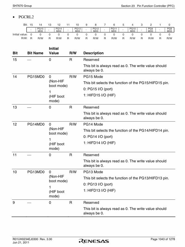
Section 23 Pin Function Controller (PFC)
R01UH0234EJ0300 Rev. 3.00 Page 1043 of 1278 Jun 21, 2011
SH7670 Group
• PGCRL2
15 14 13 12 11 10 9 8 7 6 5 4 3 2 1 0Bit:
Initial value:R/W:
0 0 0 0 0 0 0 0 0 0 0 0 0 0 0 0R R/W R R/W R R/W R R/W R R/W R R/W R R/W R R/W
PG15 MD0
PG14 MD0
PG13 MD0
PG12 MD0
PG11 MD0
PG10 MD0
PG9 MD0
PG8 MD0
- - - - - - - -
Bit Bit Name Initial Value R/W Description
15 ⎯ 0 R Reserved
This bit is always read as 0. The write value should always be 0.
14 PG15MD0 0 (Non-HIF boot mode)
1 (HIF boot mode)
R/W PG15 Mode
This bit selects the function of the PG15/HIFD15 pin.
0: PG15 I/O (port)
1: HIFD15 I/O (HIF)
13 ⎯ 0 R Reserved
This bit is always read as 0. The write value should always be 0.
12 PG14MD0 0 (Non-HIF boot mode)
1 (HIF boot mode)
R/W PG14 Mode
This bit selects the function of the PG14/HIFD14 pin.
0: PG14 I/O (port)
1: HIFD14 I/O (HIF)
11 ⎯ 0 R Reserved
This bit is always read as 0. The write value should always be 0.
10 PG13MD0 0 (Non-HIF boot mode)
1 (HIF boot mode)
R/W PG13 Mode
This bit selects the function of the PG13/HIFD13 pin.
0: PG13 I/O (port)
1: HIFD13 I/O (HIF)
9 ⎯ 0 R Reserved
This bit is always read as 0. The write value should always be 0.

Section 23 Pin Function Controller (PFC)
Page 1044 of 1278 R01UH0234EJ0300 Rev. 3.00 Jun 21, 2011
SH7670 Group
Bit Bit Name Initial Value R/W Description
8 PG12MD0 0 (Non-HIF boot mode)
1 (HIF boot mode)
R/W PG12 Mode
This bit selects the function of the PG12/HIFD12 pin.
0: PG12 I/O (port)
1: HIFD12 I/O (HIF)
7 ⎯ 0 R Reserved
This bit is always read as 0. The write value should always be 0.
6 PG11MD0 0 (Non-HIF boot mode)
1 (HIF boot mode)
R/W PG11 Mode
This bit selects the function of the PG11/HIFD11 pin.
0: PG11 I/O (port)
1: HIFD11 I/O (HIF)
5 ⎯ 0 R Reserved
This bit is always read as 0. The write value should always be 0.
4 PG10MD0 0 (Non-HIF boot mode)
1 (HIF boot mode)
R/W PG10 Mode
This bit selects the function of the PG10/HIFD10 pin.
0: PG10 I/O (port)
1: HIFD10 I/O (HIF)
3 ⎯ 0 R Reserved
This bit is always read as 0. The write value should always be 0.
2 PG09MD0 0 (Non-HIF boot mode)
1 (HIF boot mode)
R/W PG09 Mode
This bit selects the function of the PG09/HIFD09 pin.
0: PG09 I/O (port)
1: HIFD09 I/O (HIF)
1 ⎯ 0 R Reserved
This bit is always read as 0. The write value should always be 0.
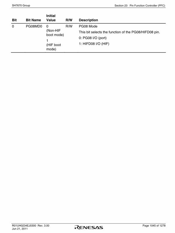
Section 23 Pin Function Controller (PFC)
R01UH0234EJ0300 Rev. 3.00 Page 1045 of 1278 Jun 21, 2011
SH7670 Group
Bit Bit Name Initial Value R/W Description
0 PG08MD0 0 (Non-HIF boot mode)
1 (HIF boot mode)
R/W PG08 Mode
This bit selects the function of the PG08/HIFD08 pin.
0: PG08 I/O (port)
1: HIFD08 I/O (HIF)

Section 23 Pin Function Controller (PFC)
Page 1046 of 1278 R01UH0234EJ0300 Rev. 3.00 Jun 21, 2011
SH7670 Group
• PGCRL1
15 14 13 12 11 10 9 8 7 6 5 4 3 2 1 0Bit:
Initial value:R/W:
0 0 0 0 0 0 0 0 0 0 0 0 0 0 0 0R R/W R R/W R R/W R R/W R R/W R R/W R R/W R R/W
PG07MD0
PG06MD0
PG05MD0
PG04MD0
PG03MD0
PG02MD0
PG01MD0
PG00MD0
- - - - - - - -
Bit Bit Name Initial Value R/W Description
15 ⎯ 0 R Reserved
This bit is always read as 0. The write value should always be 0.
14 PG07MD0 0 (Non-HIF boot mode)
1 (HIF boot mode)
R/W PG07 Mode
This bit selects the function of the PG07/HIFD07 pin.
0: PG07 I/O (port)
1: HIFD07 I/O (HIF)
13 ⎯ 0 R Reserved
This bit is always read as 0. The write value should always be 0.
12 PG06MD0 0 (Non-HIF boot mode)
1 (HIF boot mode)
R/W PG06 Mode
This bit selects the function of the PG06/HIFD06 pin.
0: PG06 I/O (port)
1: HIFD06 I/O (HIF)
11 ⎯ 0 R Reserved
This bit is always read as 0. The write value should always be 0.
10 PG05MD0 0 (Non-HIF boot mode)
1 (HIF boot mode)
R/W PG05 Mode
This bit selects the function of the PG05/HIFD05 pin.
0: PG05 I/O (port)
1: HIFD05 I/O (HIF)
9 ⎯ 0 R Reserved
This bit is always read as 0. The write value should always be 0.

Section 23 Pin Function Controller (PFC)
R01UH0234EJ0300 Rev. 3.00 Page 1047 of 1278 Jun 21, 2011
SH7670 Group
Bit Bit Name Initial Value R/W Description
8 PG04MD0 0 (Non-HIF boot mode)
1 (HIF boot mode)
R/W PG04 Mode
This bit selects the function of the PG04/HIFD04 pin.
0: PG04 I/O (port)
1: HIFD04 I/O (HIF)
7 ⎯ 0 R Reserved
This bit is always read as 0. The write value should always be 0.
6 PG03MD0 0 (Non-HIF boot mode)
1 (HIF boot mode)
R/W PG03 Mode
This bit selects the function of the PG03/HIFD03 pin.
0: PG03 I/O (port)
1: HIFD03 I/O (HIF)
5 ⎯ 0 R Reserved
This bit is always read as 0. The write value should always be 0.
4 PG02MD0 0 (Non-HIF boot mode)
1 (HIF boot mode)
R/W PG02 Mode
This bit selects the function of the PG02/HIFD02 pin.
0: PG02 I/O (port)
1: HIFD02 I/O (HIF)
3 ⎯ 0 R Reserved
This bit is always read as 0. The write value should always be 0.
2 PG01MD0 0 (Non-HIF boot mode)
1 (HIF boot mode)
R/W PG01 Mode
This bit selects the function of the PG01/HIFD01 pin.
0: PG01 I/O (port)
1: HIFD01 I/O (HIF)
1 ⎯ 0 R Reserved
This bit is always read as 0. The write value should always be 0.

Section 23 Pin Function Controller (PFC)
Page 1048 of 1278 R01UH0234EJ0300 Rev. 3.00 Jun 21, 2011
SH7670 Group
Bit Bit Name Initial Value R/W Description
0 PG00MD0 0 (Non-HIF boot mode)
1 (HIF boot mode)
R/W PG00 Mode
This bit selects the function of the PG00/HIFD00 pin.
0: PG00 I/O (port)
1: HIFD00 I/O (HIF)

Section 24 I/O Ports
R01UH0234EJ0300 Rev. 3.00 Page 1049 of 1278 Jun 21, 2011
SH7670 Group
Section 24 I/O Ports
This LSI has seven general I/O ports: A to G. Port A is an 9-bit I/O port, port B an 8-bit I/O port, port C a 21-bit I/O port, port D an 8-bit I/O port, port E a 12-bit I/O port, port F a 12-bit I/O port and port G a 24-bit I/O port.
All port pins are multiplexed with other pin functions. The functions of the multiplexed pins are selected using the pin function controller (PFC). Each port is provided with a data register for storing the pin data.
24.1 Port A
Port A is an I/O port with 9 pins shown in figure 24.1.
PA17 (input/output)/ A17 (output)
PA18 (input/output)/ A18 (output)
PA19 (input/output)/ A19 (output)
PA20 (input/output)/ A20 (output)
PA21 (input/output)/ A21 (output)
PA22 (input/output)/ A22 (output)
PA23 (input/output / A23 (output
PA24 (input/output)/ A24 (output)
PA25 (input/output)/ A25 (output)
Por
t A
Figure 24.1 Port A
24.1.1 Register Descriptions
Port A is a 9-bit I/O port. Port A has the following register. Refer to section 28, List of Registers, for more details on the addresses and states of this register in each operating mode.
Port A Data Register H (PADRH)

Section 24 I/O Ports
Page 1050 of 1278 R01UH0234EJ0300 Rev. 3.00 Jun 21, 2011
SH7670 Group
24.1.2 Port A Data Register H (PADRH)
PADRH is a 16-bit readable/writable register that stores port A data. Bits PA25DR to PA17DR correspond to pins PA25 to PA17, respectively (description of the other functions are omitted).
If a pin is set to the general output function, the pin will output the value written to the corresponding bit in PADRH, and the register value is read from PADRH regardless of the state of the pin.
If a pin is set to the general input function, the pin state, not the register value, will be returned if PADRH is read. Also, if a value is written to PADRH, although the value will actually be written, it will have no influence on the state of the pin. Table 24.1 summarizes the PADRH read/write operations.
15 14 13 12 11 10 9 8 7 6 5 4 3 2 1 0Bit:
Initial value:R/W:
0 0 0 0 0 0 0 0 0 0 0 0 0 0 0 0R R R R R R R R R/W R/W R/W R/W R/W R/W R/W R/W
- - - - - - PB7DR
PB6DR
PB5DR
PB4DR
PB3DR
PB2DR
PB1DR
PB0DR- -
Bit Bit Name Initial Value R/W Description
15 to 10
— All 0 R Reserved
These bits are always read as 0. The write value should always be 0.
9 PA25DR 0 R/W
8 PA24DR 0 R/W
7 PA23DR 0 R/W
6 PA22DR 0 R/W
5 PA21DR 0 R/W
4 PA20DR 0 R/W
3 PA19DR 0 R/W
2 PA18DR 0 R/W
1 PA17DR 0 R/W
See table 24.1.
0 — 0 R Reserved
These bits are always read as 0. The write value should always be 0.

Section 24 I/O Ports
R01UH0234EJ0300 Rev. 3.00 Page 1051 of 1278 Jun 21, 2011
SH7670 Group
Table 24.1 Port A Data Registers H (PADRH) Read/Write Operations
Bits 9 to 1 of PADRH
Pin Function PAIORH Read Write
General input 0 Pin state The value is written to PADRH but there is no effect on the pin state.
General output 1 Value of PADRH
The value written is output from the pin.
Other functions * Value of PADRH
The value is written to PADRH but there is no effect on the pin state.

Section 24 I/O Ports
Page 1052 of 1278 R01UH0234EJ0300 Rev. 3.00 Jun 21, 2011
SH7670 Group
24.2 Port B
Port B is an I/O port with 8 pins shown in figure 24.2.
PB07 (input/outpu)/BS (output)
PB06 (input)/CS4 (output)
PB05 (input/output)/CS5 (output)/CE1A (output)/IRQ3 (input)/TEND1 (output)
PB02 (input)/SE2B (output)/IRQ1 (input)
PB03 (input)/CS6 (output)/CE1B (output)/IRQ1 (input)/DREQ1 (input)
PB04 (input/output)/CE2A (output)/IRQ2 (input)/DACK1 (output)
PB01 (input)/IOIS16 (input)/SCL (input/output)
PB00 (input)/WAIT (input)/SDA (input/output)
Por
t B
Figure 24.2 Port B
24.2.1 Register Descriptions
Port B is an 8-bit I/O port. Port B has the following register. Refer to section 28, List of Registers, for more details on the addresses and states of this register in each operating mode.
Port B Data Register L (PBDRL)

Section 24 I/O Ports
R01UH0234EJ0300 Rev. 3.00 Page 1053 of 1278 Jun 21, 2011
SH7670 Group
24.2.2 Port B Data Register L (PBDRL)
PBDRL is a 16-bit readable/writable register that stores port B data. Bits PB7DR to PB0DR correspond to pins PB07 to PB00, respectively (description of the other functions are omitted).
If a pin is set to the general output function, the pin will output the value written to the corresponding bit in PBDRL, and the register value is read from PBDRL regardless of the state of the pin.
If a pin is set to the general input function, the pin state, not the register value, will be returned if PBDRL is read. Also, if a value is written to PBDRL, although the value will actually be written, it will have no influence on the state of the pin. Table 24.2 summarizes the PBDRL read/write operations.
15 14 13 12 11 10 9 8 7 6 5 4 3 2 1 0Bit:
Initial value:R/W:
0 0 0 0 0 0 0 0 0 0 0 0 0 0 0 0R R R R R R R R R/W R/W R/W R/W R/W R/W R/W R/W
- - - - - - PB7DR
PB6DR
PB5DR
PB4DR
PB3DR
PB2DR
PB1DR
PB0DR- -
Bit
Bit Name
Initial Value
R/W
Description
15 to 8 — All 0 R Reserved
These bits are always read as 0. The write value should always be 0.
7 PB7DR 0 R/W
6 PB6DR 0 R/W
5 PB5DR 0 R/W
4 PB4DR 0 R/W
3 PB3DR 0 R/W
2 PB2DR 0 R/W
1 PB1DR 0 R/W
0 PB0DR 0 R/W
See table 24.2.

Section 24 I/O Ports
Page 1054 of 1278 R01UH0234EJ0300 Rev. 3.00 Jun 21, 2011
SH7670 Group
Table 24.2 Port B Data Registers L (PBDRL) Read/Write Operations
Bits 7, 5 and 4 of PBDRL
Pin Function PBIORL Read Write
General input 0 Pin state The value is written to PBDRL but there is no effect on the pin state.
General output 1 Value of PBDRL The value written is output from the pin.
Other functions * Value of PBDRL The value is written to PBDRL but there is no effect on the pin state.
Bits 6 and 3 to 0 of PBDRL
Pin Function PBIORL Read Write
General input 0 Pin state The value is written to PBDRL but there is no effect on the pin state.
Setting prohibited 1 — —
Other functions * Value of PBDRL The value is written to PBDRL but there is no effect on the pin state.

Section 24 I/O Ports
R01UH0234EJ0300 Rev. 3.00 Page 1055 of 1278 Jun 21, 2011
SH7670 Group
24.3 Port C
Port C is an I/O port with 21 pins shown in figure 24.3.
PC09(input/output)/RX_ER (input)
PC08(input/output)/RX_DV (input)
PC07(input/output)/MII_TXD3 (output)
PC06(input/output)/MII_TXD2 (output)
PC05(input/output)/MII_TXD1 (output)
PC02(input/output)/MII_RXD2 (input)
PC03(input/output)/MII_RXD3 (input)
PC04(input/output)/MII_TXD0 (output)
PC01(input/output)/MII_RXD1 (input)
PC00(input/output)/MII_RXD0 (input)
PC10(input/output)/RX_CLK( input)
PC11(input/output)/TX_ER (output)
PC12(input/output)/TX_EN (output)
PC13(input/output)/X_CLK (input)
PC14(input/output)COL (input)
PC15(input/output)/CRS(input)
PC16(input/output)/MDIO (input/output)
PC17(input/output)/MDC (output)
PC18(input/output)/LNKSTA (input)
PC19(input/output)/EXOUT (output)
PC20(input/output)/WOL (output)
Por
t C
Figure 24.3 Port C
24.3.1 Register Descriptions
Port C is a 21-bit I/O port. Port C has the following registers. Refer to section 28, List of Registers, for more details on the addresses and states of these registers in each operating mode.
Port C Data Register H (PCDRH)
Port C Data Register L (PCDRL)

Section 24 I/O Ports
Page 1056 of 1278 R01UH0234EJ0300 Rev. 3.00 Jun 21, 2011
SH7670 Group
24.3.2 Port C Data Registers H and L (PCDRH and PCDRL)
PCDRH and PCDRL are 16-bit readable/writable registers that store port C data. Bits PC20DR to PC0DR correspond to pins PC20 to PC00, respectively (description of the other functions are omitted).
If a pin is set to the general output function, the pin will output the value written to the corresponding bit in PCDRH or PCDRL, and the register value is read from PCDRH or PCDRL regardless of the state of the pin.
If a pin is set to the general input function, the pin state, not the register value, will be returned if PCDRH or PCDRL is read. Also, if a value is written to PCDRH or PCDRL, although the value will actually be written, it will have no influence on the state of the pin. Table 24.3 summarizes the PCDRH and PCDRL read/write operations.
• PCDRH
15 14 13 12 11 10 9 8 7 6 5 4 3 2 1 0Bit:
Initial value:R/W:
0 0 0 0 0 0 0 0 0 0 0 0 0 0 0 0R R R R R R R R R R R R/W R/W R/W R/W R/W
- - - - - - PC20DR
PC19DR
PC18DR
PC17DR
PC16DR
- - - - -
Bit Bit Name
Initial Value R/W Description
15 to 5 — All 0 R Reserved
These bits are always read as 0. The write value should always be 0.
4 PC20DR 0 R/W
3 PC19DR 0 R/W
2 PC18DR 0 R/W
1 PC17DR 0 R/W
0 PC16DR 0 R/W
See table 24.3.
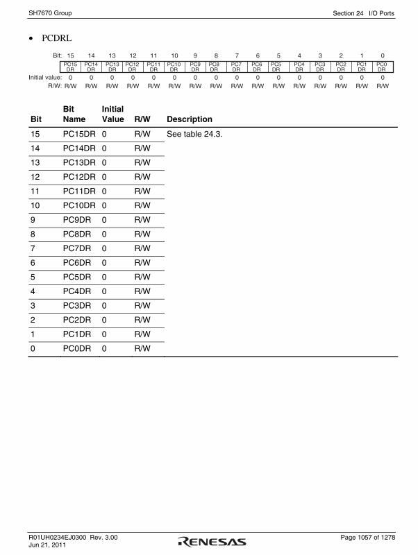
Section 24 I/O Ports
R01UH0234EJ0300 Rev. 3.00 Page 1057 of 1278 Jun 21, 2011
SH7670 Group
• PCDRL
15 14 13 12 11 10 9 8 7 6 5 4 3 2 1 0Bit:
Initial value:R/W:
0 0 0 0 0 0 0 0 0 0 0 0 0 0 0 0R/W R/W R/W R/W R/W R/W R/W R/W R/W R/W R/W R/W R/W R/W R/W R/W
PC8DR
PC15DR
PC14DR
PC13DR
PC12DR
PC11DR
PC10DR
PC9DR
PC2 DR
PC1DR
PC0DR
PC7 DR
PC6 DR
PC5 DR
PC4 DR
PC3 DR
Bit Bit Name
Initial Value R/W Description
15 PC15DR 0 R/W See table 24.3.
14 PC14DR 0 R/W
13 PC13DR 0 R/W
12 PC12DR 0 R/W
11 PC11DR 0 R/W
10 PC10DR 0 R/W
9 PC9DR 0 R/W
8 PC8DR 0 R/W
7 PC7DR 0 R/W
6 PC6DR 0 R/W
5 PC5DR 0 R/W
4 PC4DR 0 R/W
3 PC3DR 0 R/W
2 PC2DR 0 R/W
1 PC1DR 0 R/W
0 PC0DR 0 R/W
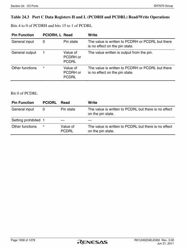
Section 24 I/O Ports
Page 1058 of 1278 R01UH0234EJ0300 Rev. 3.00 Jun 21, 2011
SH7670 Group
Table 24.3 Port C Data Registers H and L (PCDRH and PCDRL) Read/Write Operations
Bits 4 to 0 of PCDRH and bits 15 to 1 of PCDRL
Pin Function PCIORH, L Read Write
General input 0 Pin state The value is written to PCDRH or PCDRL but there is no effect on the pin state.
General output 1 Value of PCDRH or PCDRL
The value written is output from the pin.
Other functions * Value of PCDRH or PCDRL
The value is written to PCDRH or PCDRL but there is no effect on the pin state.
Bit 0 of PCDRL
Pin Function PCIORL Read Write
General input 0 Pin state The value is written to PCDRL but there is no effect on the pin state.
Setting prohibited 1 — —
Other functions * Value of PCDRL
The value is written to PCDRL but there is no effect on the pin state.

Section 24 I/O Ports
R01UH0234EJ0300 Rev. 3.00 Page 1059 of 1278 Jun 21, 2011
SH7670 Group
24.4 Port D
Port D is an I/O port with 8 pins shown in figure 24.4.
PD0 (input/output)/IRQ0 (input)/SDDAT0 (input/output)
PD1 (input/output)/IRQ1(input)/SDDAT1 (input/output)
PD2 (input/output)/IRQ2 (input)/SDDA2 (input/output)
PD3 (input/output)/IRQ3 (input)/SDDA3 (input/output)
PD4 (input)/IRQ4 (input)/ SDWP (input)
PD5 (input)/IRQ5 (input)/ SDCD (input)
PD6 (input/output)/IRQ6 (input)/SDCMD (input/output)
PD7 (input/output)/IRQ7 (input)/SDCLK (output)
Por
t D
Figure 24.4 Port D
24.4.1 Register Descriptions
Port D is an 8-bit I/O port. Port D has the following register. Refer to section 28, List of Registers, for more details on the addresses and states of this register in each operating mode.
Port D Data Register L (PDDRL)

Section 24 I/O Ports
Page 1060 of 1278 R01UH0234EJ0300 Rev. 3.00 Jun 21, 2011
SH7670 Group
24.4.2 Port D Data Register L (PDDRL)
PDDRL is a 16-bit readable/writable register that stores port D data. Bits PD7DR to PD0DR correspond to pins PD7 to PD0, respectively (description of the other functions are omitted).
If a pin is set to the general output function, the pin will output the value written to the corresponding bit in PDDRL, and the register value is read from PDDRL regardless of the state of the pin.
If a pin is set to the general input function, the pin state, not the register value, will be returned if PDDRL is read. Also, if a value is written to PDDRL, although the value will actually be written, it will have no influence on the state of the pin. Table 24.4 summarizes the PDDRL read/write operations.
15 14 13 12 11 10 9 8 7 6 5 4 3 2 1 0Bit:
Initial value:R/W:
0 0 0 0 0 0 0 0 0 0 0 0 0 0 0 0R R R R R R R R R/W R/W R/W R/W R/W R/W R/W R/W
- - - - - - PD7DR
PD6DR
PD5DR
PD4DR
PD3DR
PD2DR
PD1DR
PD0DR- -
Bit Bit Name
Initial Value R/W Description
15 to 8 — All 0 R Reserved
These bits are always read as 0. The write value should always be 0.
7 PD7DR 0 R/W See table 24.4.
6 PD6DR 0 R/W
5 PD5DR 0 R/W
4 PD4DR 0 R/W
3 PD3DR 0 R/W
2 PD2DR 0 R/W
1 PD1DR 0 R/W
0 PD0DR 0 R/W

Section 24 I/O Ports
R01UH0234EJ0300 Rev. 3.00 Page 1061 of 1278 Jun 21, 2011
SH7670 Group
Table 24.4 Port D Data Registers L (PDDRL) Read/Write Operations
Bits 7, 6, and 3 to 0 of PDDRL
Pin Function PDIORL Read Write
General input 0 Pin state The value is written to PDDRL but there is no effect on the pin state.
General output 1 Value of PDDRL The value written is output from the pin.
Other functions * Value of PDDRL The value is written to PDDRL but there is no effect on the pin state.
Bits 5 and 4 of PDDRL
Pin Function PDIORL Read Write
General input 0 Pin state The value is written to PDDRL but there is no effect on the pin state.
Setting prohibited 1 — —
Other functions * Value of PDDRL The value is written to PDDRL but there is no effect on the pin state.

Section 24 I/O Ports
Page 1062 of 1278 R01UH0234EJ0300 Rev. 3.00 Jun 21, 2011
SH7670 Group
24.5 Port E
Port E is an I/O port with 12 pins shown in figure 24.5.
PE00 (input/output)/ TS1_D0 (input)/RxD2 (input)
PE01 (input/output)/ TS1_D1 (output)/TxD2 (output)
PE02 (input/output)/TS1_D2 (input)/RxD1 (input)
PE03 (input/output)/ TS1_D3 (input/output)/SCK1 (input/output)
PE04 (input/output)/ TS1_D4 (input/output)/CTS1 (input/output)
PE05 (input/output)/TS1_D5 (input/output)/RTS1 (input/output)
PE06 (input/output)/ TS1_D6 (input/output)/SSIDATA1 (input/output)
PE07 (input/output)/ TS1_D7 (input/output)/SSIWS1 (input/output)
PE08 (input/output)/ TS1_REQ (output)/TxD2 (output)
PE09 (input/output)/ TS1_VLD (input/output)/SCK2 (input/output)
PE11 (input/output)/ TS1_PWM (output)/RTS2 (input/output)
Por
t E
PE10 (input/output)/ TS1_SYC (input/output)/CTS2 (input/output)
Figure 24.5 Port E
24.5.1 Register Descriptions
Port E is a 12-bit I/O port. Port E has the following register. Refer to section 28, List of Registers, for more details on the addresses and states of this register in each operating mode.
Port E Data Register L (PEDRL)

Section 24 I/O Ports
R01UH0234EJ0300 Rev. 3.00 Page 1063 of 1278 Jun 21, 2011
SH7670 Group
24.5.2 Port E Data Register L (PEDRL)
PEDRL is a 16-bit readable/writable register that stores port E data. Bits PE11DR to PE0DR correspond to pins PE11 to PE00, respectively (description of the other functions are omitted).
If a pin is set to the general output function, the pin will output the value written to the corresponding bit in PEDRL, and the register value is read from PEDRL regardless of the state of the pin.
If a pin is set to the general input function, the pin state, not the register value, will be returned if PEDRL is read. Also, if a value is written to PEDRL, although the value will actually be written, it will have no influence on the state of the pin. Table 24.5 summarizes the PEDRL read/write operations.
15 14 13 12 11 10 9 8 7 6 5 4 3 2 1 0Bit:
Initial value:R/W:
0 0 0 0 0 0 0 0 0 0 0 0 0 0 0 0R R R R R/W R/W R/W R/W R/W R/W R/W R/W R/W R/W R/W R/W
- - - - PE9 DR
PE8DR
PE7 DR
PE6 DR
PE5 DR
PE4 DR
PE3 DR
PE2 DR
PE11DR
PE10DR
PE1 DR
PE0 DR
Bit
Bit Name
Initial Value
R/W
Description
15 to 12
— All 0 R Reserved
These bits are always read as 0. The write value should always be 0.
11 PE11DR 0 R/W See table 24.5.
10 PE10DR 0 R/W
9 PE9DR 0 R/W
8 PE8DR 0 R/W
7 PE7DR 0 R/W
6 PE6DR 0 R/W
5 PE5DR 0 R/W
4 PE4DR 0 R/W
3 PE3DR 0 R/W
2 PE2DR 0 R/W
1 PE1DR 0 R/W
0 PE0DR 0 R/W

Section 24 I/O Ports
Page 1064 of 1278 R01UH0234EJ0300 Rev. 3.00 Jun 21, 2011
SH7670 Group
Table 24.5 Port E Data Registers L (PEDRL) Read/Write Operations
Bits 11 and 0 of PEDRL
Pin Function PEIORL Read Write
General input 0 Pin state The value is written to PEDRL but there is no effect on the pin state.
General output 1 Value of PEDRL
The value written is output from the pin.
Other functions * Value of PEDRL
The value is written to PEDRL but there is no effect on the pin state.

Section 24 I/O Ports
R01UH0234EJ0300 Rev. 3.00 Page 1065 of 1278 Jun 21, 2011
SH7670 Group
24.6 Port F
Port F is an I/O port with 12 pins shown in figure 24.6.
PF00 (input/outoput)/ TS0_D0 (input/output)
PF01 (input/outoput)/ TS0_D1 (output)/TxD0 (output)
PF02 (input/outoput)/ TS0_D2 (input/output)/RxD0 (input)
PF03 (input/outoput)/ TS0_D3 (input/output)/SCKO0 (input/output)
PF04 (input/outoput)/ TS0_D4 (input/output)/CTS0 (input/output)
PF05 (input/outoput)/ TS0_D5 (input/output)/RTS0 (input/output)
PF06 (input/outoput)/ TS0_D6 (input/output)/SSIDATA0 (input/output)
PF07 (input/outoput)/ TS0_D7 (input/output)/SSIWS0 (input/output)
PF08 (input/outoput)/ TS0_REQ (input/output)
PF09 (input/outoput)/ TS0_VLD (input/output)/DREQ0 (input)
PF10 (input/outoput)/ TS0_SYC (input/output)/DACK0 (output)
PF11 (input/outoput)/ TS0_PWM (output)/TEND0 (output)
Por
t F
Figure 24.6 Port F
24.6.1 Register Descriptions
Port F is an 12-bit I/O port. Port F has the following register. Refer to section 28, List of Registers, for more details on the addresses and states of this register in each operating mode.
Port F Data Register L (PFDRL)

Section 24 I/O Ports
Page 1066 of 1278 R01UH0234EJ0300 Rev. 3.00 Jun 21, 2011
SH7670 Group
24.6.2 Port F Data Register L (PFDRL)
PFDRL is a 16-bit readable/writable register that stores port F data. Bits PF11DR to PF0DR correspond to pins PF11 to PF00, respectively (description of the other functions are omitted).
If a pin is set to the general output function, the pin will output the value written to the corresponding bit in PFDRL, and the register value is read from PFDRL regardless of the state of the pin.
If a pin is set to the general input function, the pin state, not the register value, will be returned if PFDRL is read. Also, if a value is written to PFDRL, although the value will actually be written, it will have no influence on the state of the pin. Table 24.6 summarizes the PFDRL read/write operations.
15 14 13 12 11 10 9 8 7 6 5 4 3 2 1 0Bit:
Initial value:R/W:
0 0 0 0 0 0 0 0 0 0 0 0 0 0 0 0R R R R R/W R/W R/W R/W R/W R/W R/W R/W R/W R/W R/W R/W
- - - - PF9 DR
PF8DR
PF7 DR
PF6 DR
PF5 DR
PF4 DR
PF3 DR
PF2 DR
PF11DR
PF10DR
PF1 DR
PF0 DR
Bit
Bit Name
Initial Value
R/W
Description
15 to 12
— All 0 R Reserved
These bits are always read as 0. The write value should always be 0.
11 PF11DR 0 R/W See table 24.6.
10 PF10DR 0 R/W
9 PF9DR 0 R/W
8 PF8DR 0 R/W
7 PF7DR 0 R/W
6 PF6DR 0 R/W
5 PF5DR 0 R/W
4 PF4DR 0 R/W
3 PF3DR 0 R/W
2 PF2DR 0 R/W
1 PF1DR 0 R/W
0 PF0DR 0 R/W

Section 24 I/O Ports
R01UH0234EJ0300 Rev. 3.00 Page 1067 of 1278 Jun 21, 2011
SH7670 Group
Table 24.6 Port F Data Registers L (PFDRL) Read/Write Operations
Bits 11 and 0 of PFDRL
Pin Function PFIORL Read Write
General input 0 Pin state The value is written to PFDRL but there is no effect on the pin state.
General output 1 Value of PFDRL
The value written is output from the pin.
Other functions * Value of PFDRL
The value is written to PFDRL but there is no effect on the pin state.

Section 24 I/O Ports
Page 1068 of 1278 R01UH0234EJ0300 Rev. 3.00 Jun 21, 2011
SH7670 Group
24.7 Port G
Port G is an I/O port with 24 pins shown in figure 24.7.
PC09 (input/output)/HIFD09 (input/output)
PC08 (input/output)/HIFD08 (input/output)
PC07 (input/output)/HIFD07 (input/output)
PC06 (input/output)/HIFD06 (input/output)
PC05 (input/output)/HIFD05 (input/output)
PC04 (input/output)/HIFD04 (input/output)
PC10 (input/output)/HIFD10 (input/output)
PC11 (input/output)/HIFD11 (input/output)
PC12( input/output)/HIFD12 (input/output)
PC13 (input/output)/HIFD13 (input/output)
PC14 (input/output)/HIFD14 (input/output)
PC15( input/output)/HIFD15 (input/output)
PC16 (input/output)/HIFEBL (input)
PC17(input/output)/HIFRDY (output)
PC18 (input/output)/HIFDREQ (output)
PC19 (input/output)/HIFINT (output)
PC20 (input/output)/HIFRD (input)
PC23 (input/output)/HIFCS (input)
PC22 (input/output)/HIFRS (input)
PC21 (input/output)/HIFWR (input)
PC00 (input/output)/HIFD00 (input/output)
PC01 (input/output)/HIFD01 (input/output)
PC02 (input/output)/HIFD02 (input/output)
PC03 (input/output)/HIFD03 (input/output)
Por
t G
Figure 24.7 Port G

Section 24 I/O Ports
R01UH0234EJ0300 Rev. 3.00 Page 1069 of 1278 Jun 21, 2011
SH7670 Group
24.7.1 Register Descriptions
Port G is a 24-bit I/O port. Port G has the following registers. Refer to section 28, List of Registers, for more details on the addresses and states of these registers in each operating mode.
Port G Data Register H (PGDRH)
Port G Data Register L (PGDRL)
24.7.2 Port G Data Registers H and L (PGDRH and PGDRL)
PGDRH and PGDRL are 16-bit readable/writable registers that store port G data. Bits PG23DR to PG0DR correspond to pins PG23 to PG00, respectively (description of the other functions are omitted).
If a pin is set to the general output function, the pin will output the value written to the corresponding bit in PGDRH or PGDRL, and the register value is read from PGDRH or PGDRL regardless of the state of the pin.
If a pin is set to the general input function, the pin state, not the register value, will be returned if PGDRH or PGDRL is read. Also, if a value is written to PGDRH or PGDRL, although the value will actually be written, it will have no influence on the state of the pin. Table 24.7 summarizes the PGDRH and PGDRL read/write operations.

Section 24 I/O Ports
Page 1070 of 1278 R01UH0234EJ0300 Rev. 3.00 Jun 21, 2011
SH7670 Group
• PGDRH
15 14 13 12 11 10 9 8 7 6 5 4 3 2 1 0Bit:
Initial value:R/W:
0 0 0 0 0 0 0 0 0 0 0 0 0 0 0 0R R R R R R R R R/W R/W R/W R/W R/W R/W R/W R/W
- - - - - - PG23 DR
PG22 DR
PG21 DR
PG20 DR
PG19 DR
PG18 DR
PG17 DR
PG16 DR- -
Bit Bit Name Initial Value R/W Description
15 to 8 — All 0 R Reserved
These bits are always read as 0. The write value should always be 0.
7 PG23DR 0 R/W See table 24.7.
6 PG22DR 0 R/W
5 PG21DR 0 R/W
4 PG20DR 0 R/W
3 PG19DR 0 R/W
2 PG18DR 0 R/W
1 PG17DR 0 R/W
0 PG16DR 0 R/W

Section 24 I/O Ports
R01UH0234EJ0300 Rev. 3.00 Page 1071 of 1278 Jun 21, 2011
SH7670 Group
• PGDRL
15 14 13 12 11 10 9 8 7 6 5 4 3 2 1 0Bit:
Initial value:R/W:
0 0 0 0 0 0 0 0 0 0 0 0 0 0 0 0R/W R/W R/W R/W R/W R/W R/W R/W R/W R/W R/W R/W R/W R/W R/W R/W
PG8DR
PG15DR
PG14DR
PG13DR
PG12DR
PG11DR
PG10DR
PG9DR
PG2 DR
PG1DR
PG0DR
PG7 DR
PG6 DR
PG5 DR
PG4 DR
PG3 DR
Bit
Bit Name
Initial Value
R/W
Description
15 PG15DR 0 R/W See table 24.7.
14 PG14DR 0 R/W
13 PG13DR 0 R/W
12 PG12DR 0 R/W
11 PG11DR 0 R/W
10 PG10DR 0 R/W
9 PG9DR 0 R/W
8 PG8DR 0 R/W
7 PG7DR 0 R/W
6 PG6DR 0 R/W
5 PG5DR 0 R/W
4 PG4DR 0 R/W
3 PG3DR 0 R/W
2 PG2DR 0 R/W
1 PG1DR 0 R/W
0 PG0DR 0 R/W
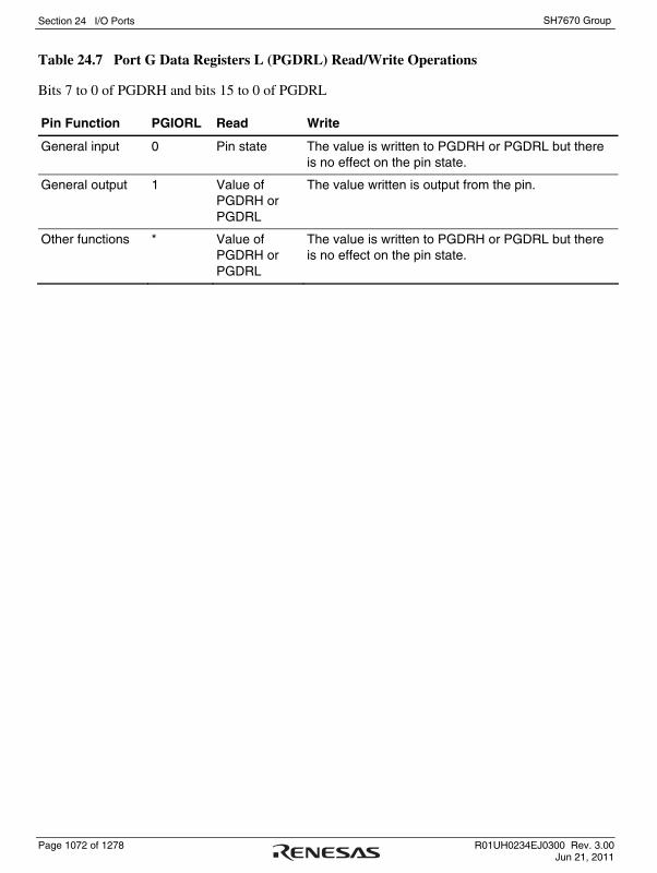
Section 24 I/O Ports
Page 1072 of 1278 R01UH0234EJ0300 Rev. 3.00 Jun 21, 2011
SH7670 Group
Table 24.7 Port G Data Registers L (PGDRL) Read/Write Operations
Bits 7 to 0 of PGDRH and bits 15 to 0 of PGDRL
Pin Function PGIORL Read Write
General input 0 Pin state The value is written to PGDRH or PGDRL but there is no effect on the pin state.
General output 1 Value of PGDRH or PGDRL
The value written is output from the pin.
Other functions * Value of PGDRH or PGDRL
The value is written to PGDRH or PGDRL but there is no effect on the pin state.

Section 25 User Break Controller (UBC)
R01UH0234EJ0300 Rev. 3.00 Page 1073 of 1278 Jun 21, 2011
SH7670 Group
Section 25 User Break Controller (UBC)
The user break controller (UBC) provides functions that simplify program debugging. These functions make it easy to design an effective self-monitoring debugger, enabling the chip to debug programs without using an in-circuit emulator. Instruction fetch or data read/write (bus master (CPU or DMAC) selection in the case of data read/write), data size, data contents, address value, and stop timing in the case of instruction fetch are break conditions that can be set in the UBC. Since this LSI uses a Harvard architecture, instruction fetch on the CPU bus (C bus) is performed by issuing bus cycles on the instruction fetch bus (F bus), and data access on the C bus is performed by issuing bus cycles on the memory access bus (M bus). The UBC monitors the C bus and internal bus (I bus).
25.1 Features
1. The following break comparison conditions can be set.
Number of break channels: two channels (channels 0 and 1)
User break can be requested as the independent condition on channels 0 and 1.
• Address
Comparison of the 32-bit address is maskable in 1-bit units.
One of the three address buses (F address bus (FAB), M address bus (MAB), and I address bus (IAB)) can be selected.
• Data
Comparison of the 32-bit data is maskable in 1-bit units.
One of the two data buses (M data bus (MDB) and I data bus (IDB)) can be selected.
• Bus master when I bus is selected
Selection of CPU cycles, DMAC cycles, A-DMAC (including F-DMAC) cycles, or E-DMAC cycles
• Bus cycle
Instruction fetch (only when C bus is selected) or data access
• Read/write
• Operand size
Byte, word, and longword
2. In an instruction fetch cycle, it can be selected whether the start of user break interrupt exception processing is set before or after an instruction is executed.

Section 25 User Break Controller (UBC)
Page 1074 of 1278 R01UH0234EJ0300 Rev. 3.00 Jun 21, 2011
SH7670 Group
Figure 25.1 shows a block diagram of the UBC.
IDB IAB MAB FABMDB
BBR_0
BBR_1
BAR_0
BAMR_0
BDR_0
BDMR_0
BAR_1
BAMR_1
BDR_1
BDMR_1
BRCR
I bus
Accesscomparator
Addresscomparator
Channel 0
Accesscomparator
Addresscomparator
Datacomparator
Control
Channel 1
User break interrupt request
[Legend]BBR:BAR:BAMR:
BDR:BDMR:BRCR:
Break bus cycle registerBreak address registerBreak address mask register
Access control
Datacomparator
UBCTRG pin output
I bus C bus
Break data registerBreak data mask registeBreak control register
Figure 25.1 Block Diagram of UBC

Section 25 User Break Controller (UBC)
R01UH0234EJ0300 Rev. 3.00 Page 1075 of 1278 Jun 21, 2011
SH7670 Group
25.2 Register Descriptions
The UBC has the following registers. Five control registers for each channel and one common control register for channel 0 and channel 1 are available. A register for each channel is described as BAR_0 for the BAR register in channel 0.
Table 25.1 Register Configuration
Channel Register Name Abbrevia- tion R/W Initial Value Address
Access Size
Break address register_0 BAR_0 R/W H'00000000 H'FFFC0400 32
Break address mask register_0 BAMR_0 R/W H'00000000 H'FFFC0404 32
Break bus cycle register_0 BBR_0 R/W H'0000 H'FFFC04A0 16
Break data register_0 BDR_0 R/W H'00000000 H'FFFC0408 32
0
Break data mask register_0 BDMR_0 R/W H'00000000 H'FFFC040C 32
Break address register_1 BAR_1 R/W H'00000000 H'FFFC0410 32
Break address mask register_1 BAMR_1 R/W H'00000000 H'FFFC0414 32
Break bus cycle register_1 BBR_1 R/W H'0000 H'FFFC04B0 16
Break data register_1 BDR_1 R/W H'00000000 H'FFFC0418 32
1
Break data mask register_1 BDMR_1 R/W H'00000000 H'FFFC041C 32
Common Break control register BRCR R/W H'00000000 H'FFFC04C0 32
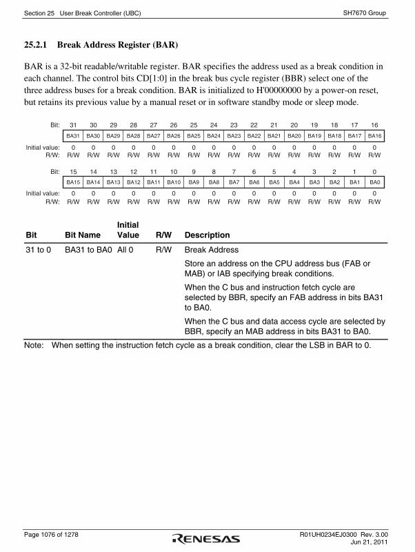
Section 25 User Break Controller (UBC)
Page 1076 of 1278 R01UH0234EJ0300 Rev. 3.00 Jun 21, 2011
SH7670 Group
25.2.1 Break Address Register (BAR)
BAR is a 32-bit readable/writable register. BAR specifies the address used as a break condition in each channel. The control bits CD[1:0] in the break bus cycle register (BBR) select one of the three address buses for a break condition. BAR is initialized to H'00000000 by a power-on reset, but retains its previous value by a manual reset or in software standby mode or sleep mode.
31 30 29 28 27 26 25 24 23 22 21 20 19 18 17 16
15 14 13 12 11 10 9 8 7 6 5 4 3 2 1 0
0 0 0 0 0 0 0 0 0 0 0 0 0 0 0 0R/W R/W R/W R/W R/W R/W R/W R/W R/W R/W R/W R/W R/W R/W R/W R/W
0 0 0 0 0 0 0 0 0 0 0 0 0 0 0 0R/W R/W R/W R/W R/W R/W R/W R/W R/W R/W R/W R/W R/W R/W R/W R/W
Bit:
Initial value:R/W:
Bit:
Initial value:R/W:
BA31 BA30 BA29 BA28 BA27 BA26 BA25 BA24 BA23 BA22 BA21 BA20 BA19 BA18 BA17 BA16
BA15 BA14 BA13 BA12 BA11 BA10 BA9 BA8 BA7 BA6 BA5 BA4 BA3 BA2 BA1 BA0
Bit Bit Name Initial Value R/W Description
31 to 0 BA31 to BA0 All 0 R/W Break Address
Store an address on the CPU address bus (FAB or MAB) or IAB specifying break conditions.
When the C bus and instruction fetch cycle are selected by BBR, specify an FAB address in bits BA31 to BA0.
When the C bus and data access cycle are selected by BBR, specify an MAB address in bits BA31 to BA0.
Note: When setting the instruction fetch cycle as a break condition, clear the LSB in BAR to 0.
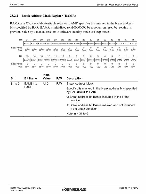
Section 25 User Break Controller (UBC)
R01UH0234EJ0300 Rev. 3.00 Page 1077 of 1278 Jun 21, 2011
SH7670 Group
25.2.2 Break Address Mask Register (BAMR)
BAMR is a 32-bit readable/writable register. BAMR specifies bits masked in the break address bits specified by BAR. BAMR is initialized to H'00000000 by a power-on reset, but retains its previous value by a manual reset or in software standby mode or sleep mode.
31 30 29 28 27 26 25 24 23 22 21 20 19 18 17 16
15 14 13 12 11 10 9 8 7 6 5 4 3 2 1 0
0 0 0 0 0 0 0 0 0 0 0 0 0 0 0 0R/W R/W R/W R/W R/W R/W R/W R/W R/W R/W R/W R/W R/W R/W R/W R/W
0 0 0 0 0 0 0 0 0 0 0 0 0 0 0 0R/W R/W R/W R/W R/W R/W R/W R/W R/W R/W R/W R/W R/W R/W R/W R/W
Bit:
Initial value:R/W:
Bit:
Initial value:R/W:
BAM31 BAM30 BAM29 BAM28 BAM27 BAM26 BAM25 BAM24 BAM23 BAM22 BAM21 BAM20 BAM19 BAM18 BAM17 BAM16
BAM15 BAM14 BAM13 BAM12 BAM11 BAM10 BAM9 BAM8 BAM7 BAM6 BAM5 BAM4 BAM3 BAM2 BAM1 BAM0
Bit Bit Name Initial Value R/W Description
31 to 0 BAM31 to BAM0
All 0 R/W Break Address Mask
Specify bits masked in the break address bits specified by BAR (BA31 to BA0).
0: Break address bit BAn is included in the break condition
1: Break address bit BAn is masked and not included in the break condition
Note: n = 31 to 0

Section 25 User Break Controller (UBC)
Page 1078 of 1278 R01UH0234EJ0300 Rev. 3.00 Jun 21, 2011
SH7670 Group
25.2.3 Break Data Register (BDR)
BDR is a 32-bit readable/writable register. The control bits CD[1:0]in the break bus cycle register (BBR) select one of the two data buses for a break condition. BDR is initialized to H'00000000 by a power-on reset, but retains its previous value by a manual reset or in software standby mode or sleep mode.
31 30 29 28 27 26 25 24 23 22 21 20 19 18 17 16
15 14 13 12 11 10 9 8 7 6 5 4 3 2 1 0
0 0 0 0 0 0 0 0 0 0 0 0 0 0 0 0R/W R/W R/W R/W R/W R/W R/W R/W R/W R/W R/W R/W R/W R/W R/W R/W
0 0 0 0 0 0 0 0 0 0 0 0 0 0 0 0R/W R/W R/W R/W R/W R/W R/W R/W R/W R/W R/W R/W R/W R/W R/W R/W
Bit:
Initial value:R/W:
Bit:
Initial value:R/W:
BD31 BD30 BD29 BD28 BD27 BD26 BD25 BD24 BD23 BD22 BD21 BD20 BD19 BD18 BD17 BD16
BD15 BD14 BD13 BD12 BD11 BD10 BD9 BD8 BD7 BD6 BD5 BD4 BD3 BD2 BD1 BD0
Bit Bit Name Initial Value R/W Description
31 to 0 BD31 to BD0 All 0 R/W Break Data Bits
Store data which specifies a break condition.
If the I bus is selected in BBR, specify the break data on IDB in bits BD31 to BD0.
If the C bus is selected in BBR, specify the break data on MDB is set in bits BD31 to BD0.
Notes: 1. Set the operand size when specifying a value on a data bus as the break condition.
2. When the byte size is selected as a break condition, the same byte data must be set in bits 31 to 24, 23 to 16, 15 to 8, and 7 to 0 in BDR as the break data. Similarly, when the word size is selected, the same word data must be set in bits 31 to 16 and 15 to 0.

Section 25 User Break Controller (UBC)
R01UH0234EJ0300 Rev. 3.00 Page 1079 of 1278 Jun 21, 2011
SH7670 Group
25.2.4 Break Data Mask Register (BDMR)
BDMR is a 32-bit readable/writable register. BDMR specifies bits masked in the break data bits specified by BDR. BDMR is initialized to H'00000000 by a power-on reset, but retains its previous value by a manual reset or in software standby mode or sleep mode.
31 30 29 28 27 26 25 24 23 22 21 20 19 18 17 16
15 14 13 12 11 10 9 8 7 6 5 4 3 2 1 0
0 0 0 0 0 0 0 0 0 0 0 0 0 0 0 0R/W R/W R/W R/W R/W R/W R/W R/W R/W R/W R/W R/W R/W R/W R/W R/W
0 0 0 0 0 0 0 0 0 0 0 0 0 0 0 0R/W R/W R/W R/W R/W R/W R/W R/W R/W R/W R/W R/W R/W R/W R/W R/W
Bit:
Initial value:R/W:
Bit:
Initial value:R/W:
BDM31 BDM30 BDM29 BDM28 BDM27 BDM26 BDM25 BDM24 BDM23 BDM22 BDM21 BDM20 BDM19 BDM18 BDM17 BDM16
BDM15 BDM14 BDM13 BDM12 BDM11 BDM10 BDM9 BDM8 BDM7 BDM6 BDM5 BDM4 BDM3 BDM2 BDM1 BDM0
Bit Bit Name Initial Value R/W Description
31 to 0 BDM31 to BDM0
All 0 R/W Break Data Mask
Specify bits masked in the break data bits specified by BDR (BD31 to BD0).
0: Break data bit BDn is included in the break condition
1: Break data bit BDn is masked and not included in the break condition
Note: n = 31 to 0
Notes: 1. Set the operand size when specifying a value on a data bus as the break condition.
2. When the byte size is selected as a break condition, the same byte data must be set in bits 31 to 24, 23 to 16, 15 to 8, and 7 to 0 in BDMR as the break mask data. Similarly, when the word size is selected, the same word data must be set in bits 31 to 16 and 15 to 0.
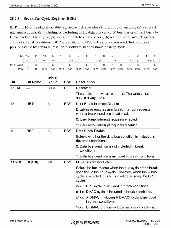
Section 25 User Break Controller (UBC)
Page 1080 of 1278 R01UH0234EJ0300 Rev. 3.00 Jun 21, 2011
SH7670 Group
25.2.5 Break Bus Cycle Register (BBR)
BBR is a 16-bit readable/writable register, which specifies (1) disabling or enabling of user break interrupt requests, (2) including or excluding of the data bus value, (3) bus master of the I bus, (4) C bus cycle or I bus cycle, (5) instruction fetch or data access, (6) read or write, and (7) operand size as the break conditions. BBR is initialized to H'0000 by a power-on reset, but retains its previous value by a manual reset or in software standby mode or sleep mode.
15 14 13 12 11 10 9 8 7 6 5 4 3 2 1 0Bit:
Initial Value:R/W:
0 0 0 0 0 0 0 0 0 0 0 0 0 0 0 0R R R/W R/W R/W R/W R/W R/W R/W R/W R/W R/W R/W R/W R/W R/W
⎯ ⎯ UBID DBE CP[3:0] CD[1:0] ID[1:0] RW[1:0] SZ[1:0]
Bit Bit Name Initial Value R/W Description
15, 14 ⎯ All 0 R Reserved
These bits are always read as 0. The write value should always be 0.
13 UBID 0 R/W User Break Interrupt Disable
Disables or enables user break interrupt requests when a break condition is satisfied.
0: User break interrupt requests enabled
1: User break interrupt requests disabled
12 DBE 0 R/W Data Break Enable
Selects whether the data bus condition is included in the break conditions.
0: Data bus condition is not included in break conditions
1: Data bus condition is included in break conditions
11 to 8 CP[3:0] 00 R/W I-Bus Bus Master Select
Select the bus master when the bus cycle of the break condition is the I bus cycle. However, when the C bus cycle is selected, this bit is invalidated (only the CPU cycle).
xxx1: CPU cycle is included in break conditions.
xx1x: DMAC cycle is included in break conditions.
x1xx: A-DMAC (including F-DMAC) cycle is included in break conditions.
1xxx: E-DMAC cycle is included in break conditions.

Section 25 User Break Controller (UBC)
R01UH0234EJ0300 Rev. 3.00 Page 1081 of 1278 Jun 21, 2011
SH7670 Group
Bit Bit Name Initial Value R/W Description
7, 6 CD[1:0] 00 R/W C Bus Cycle/I Bus Cycle Select
Select the C bus cycle or I bus cycle as the bus cycle of the break condition.
00: Condition comparison is not performed
01: Break condition is the C bus (F bus or M bus) cycle
10: Break condition is the I bus cycle
11: Break condition is the C bus (F bus or M bus) cycle
5, 4 ID[1:0] 00 R/W Instruction Fetch/Data Access Select
Select the instruction fetch cycle or data access cycle as the bus cycle of the break condition. If the instruction fetch cycle is selected, select the C bus cycle.
00: Condition comparison is not performed
01: Break condition is the instruction fetch cycle
10: Break condition is the data access cycle
11: Break condition is the instruction fetch cycle or data access cycle
3, 2 RW[1:0] 00 R/W Read/Write Select
Select the read cycle or write cycle as the bus cycle of the break condition.
00: Condition comparison is not performed
01: Break condition is the read cycle
10: Break condition is the write cycle
11: Break condition is the read cycle or write cycle
1, 0 SZ[1:0] 00 R/W Operand Size Select
Select the operand size of the bus cycle for the break condition.
00: Break condition does not include operand size
01: Break condition is byte access
10: Break condition is word access
11: Break condition is longword access
[Legend]
x: Don't care
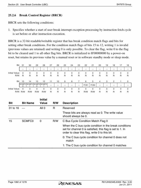
Section 25 User Break Controller (UBC)
Page 1082 of 1278 R01UH0234EJ0300 Rev. 3.00 Jun 21, 2011
SH7670 Group
25.2.6 Break Control Register (BRCR)
BRCR sets the following conditions:
1. Specifies whether a start of user break interrupt exception processing by instruction fetch cycle is set before or after instruction execution.
BRCR is a 32-bit readable/writable register that has break condition match flags and bits for setting other break conditions. For the condition match flags of bits 15 to 12, writing 1 is invalid (previous values are retained) and writing 0 is only possible. To clear the flag, write 0 to the flag bit to be cleared and 1 to all other flag bits. BRCR is initialized to H'00000000 by a power-on reset, but retains its previous value by a manual reset or in software standby mode or sleep mode.
31 30 29 28 27 26 25 24 23 22 21 20 19 18 17 16Bit:
Initial Value:R/W:
15 14 13 12 11 10 9 8 7 6 5 4 3 2 1 0Bit:
Initial Value:R/W:
0 0 0 0 0 0 0 0 0 0 0 0 0 0 0 0R R R R R R R R R R R R R R R R
0 0 0 0 0 0 0 0 0 0 0 0 0 0 0 0R/W R/W R/W R/W R R R R R R/W R/W R R R R R
⎯ ⎯ ⎯ ⎯ ⎯ ⎯ ⎯ ⎯ ⎯ ⎯ ⎯ ⎯ ⎯ ⎯
SCMFC0
SCMFC1
SCMFD0
SCMFD1 ⎯ ⎯ ⎯ ⎯ ⎯ PCB1 PCB0 ⎯ ⎯ ⎯ ⎯ ⎯
⎯ ⎯
Bit Bit Name Initial Value R/W Description
31 to 16 ⎯ All 0 R Reserved
These bits are always read as 0. The write value should always be 0.
15 SCMFC0 0 R/W C Bus Cycle Condition Match Flag 0
When the C bus cycle condition in the break conditions set for channel 0 is satisfied, this flag is set to 1. In order to clear this flag, write 0 to this bit.
0: The C bus cycle condition for channel 0 does not match
1: The C bus cycle condition for channel 0 matches

Section 25 User Break Controller (UBC)
R01UH0234EJ0300 Rev. 3.00 Page 1083 of 1278 Jun 21, 2011
SH7670 Group
Bit Bit Name Initial Value R/W Description
14 SCMFC1 0 R/W C Bus Cycle Condition Match Flag 1
When the C bus cycle condition in the break conditions set for channel 1 is satisfied, this flag is set to 1. In order to clear this flag, write 0 to this bit.
0: The C bus cycle condition for channel 1 does not match
1: The C bus cycle condition for channel 1 matches
13 SCMFD0 0 R/W I Bus Cycle Condition Match Flag 0
When the I bus cycle condition in the break conditions set for channel 0 is satisfied, this flag is set to 1. In order to clear this flag, write 0 to this bit.
0: The I bus cycle condition for channel 0 does not match
1: The I bus cycle condition for channel 0 matches
12 SCMFD1 0 R/W I Bus Cycle Condition Match Flag 1
When the I bus cycle condition in the break conditions set for channel 1 is satisfied, this flag is set to 1. In order to clear this flag, write 0 to this bit.
0: The I bus cycle condition for channel 1 does not match
1: The I bus cycle condition for channel 1 matches
11 to 7 ⎯ All 0 R Reserved
These bits are always read as 0. The write value should always be 0.
6 PCB1 0 R/W PC Break Select 1
Selects the break timing of the instruction fetch cycle for channel 1 as before or after instruction execution. 0: PC break of channel 1 is generated before
instruction execution 1: PC break of channel 1 is generated after instruction
execution
5 PCB0 0 R/W PC Break Select 0
Selects the break timing of the instruction fetch cycle for channel 0 as before or after instruction execution. 0: PC break of channel 0 is generated before
instruction execution 1: PC break of channel 0 is generated after instruction
execution
4 to 0 ⎯ All 0 R Reserved
These bits are always read as 0. The write value should always be 0.

Section 25 User Break Controller (UBC)
Page 1084 of 1278 R01UH0234EJ0300 Rev. 3.00 Jun 21, 2011
SH7670 Group
25.3 Operation
25.3.1 Flow of the User Break Operation
The flow from setting of break conditions to user break interrupt exception handling is described below:
1. The break address is set in a break address register (BAR). The masked address bits are set in a break address mask register (BAMR). The break data is set in the break data register (BDR). The masked data bits are set in the break data mask register (BDMR). The bus break conditions are set in the break bus cycle register (BBR). Three control bit groups of BBR (C bus cycle/I bus cycle select, instruction fetch/data access select, and read/write select) are each set. No user break will be generated if even one of these groups is set to 00. The relevant break control conditions are set in the bits of the break control register (BRCR). Make sure to set all registers related to breaks before setting BBR, and branch after reading from the last written register. The newly written register values become valid from the instruction at the branch destination.
2. In the case where the break conditions are satisfied and the user break interrupt request is enabled, the UBC sends a user break interrupt request to the INTC, sets the C bus condition match flag (SCMFC) or I bus condition match flag (SCMFD) for the appropriate channel.
3. On receiving a user break interrupt request signal, the INTC determines its priority. Since the user break interrupt has a priority level of 15, it is accepted when the priority level set in the interrupt mask level bits (I3 to I0) of the status register (SR) is 14 or lower. If the I3 to I0 bits are set to a priority level of 15, the user break interrupt is not accepted, but the conditions are checked, and condition match flags are set if the conditions match. For details on ascertaining the priority, see section 6, Interrupt Controller (INTC).
4. Condition match flags (SCMFC and SCMFD) can be used to check which condition has been satisfied. Clear the condition match flags during the user break interrupt exception processing routine. The interrupt occurs again if this operation is not performed.
5. There is a chance that the break set in channel 0 and the break set in channel 1 occur around the same time. In this case, there will be only one user break request to the INTC, but these two break channel match flags may both be set.
6. When selecting the I bus as the break condition, note as follows:
⎯ Several bus masters, including the CPU, DMAC, A-DMAC (including F-DMAC), and E-DMAC, are connected to the I bus. The UBC monitors bus cycles generated by the bus master specified by BBR, and determines the condition match.
Section 25 User Break Controller (UBC)
R01UH0234EJ0300 Rev. 3.00 Page 1085 of 1278 Jun 21, 2011
SH7670 Group
⎯ Whether or not an access issued on the C bus by the CPU is issued on the I bus depends on the cache settings. Regarding the I bus operation under cache conditions, see table 4.8 in section 4, Cache.
⎯ When a break condition is specified for the I bus, only the data access cycle is monitored. The instruction fetch cycle (including the cache renewal cycle) is not monitored.
⎯ The DMAC only issues data access cycles for I bus cycles.
⎯ If a break condition is specified for the I bus, even when the condition matches in an I bus cycle resulting from an instruction executed by the CPU, at which instruction the user break interrupt request is to be accepted cannot be clearly defined.
25.3.2 Break on Instruction Fetch Cycle
1. When C bus/instruction fetch/read/word or longword is set in the break bus cycle register (BBR), the break condition is the FAB bus instruction fetch cycle. Whether a start of user break interrupt exception processing is set before or after the execution of the instruction can then be selected with the PCB0 or PCB1 bit of the break control register (BRCR) for the appropriate channel. If an instruction fetch cycle is set as a break condition, clear BA0 bit in the break address register (BAR) to 0. A break cannot be generated as long as this bit is set to 1.
2. A break for instruction fetch which is set as a break before instruction execution occurs when it is confirmed that the instruction has been fetched and will be executed. This means a break does not occur for instructions fetched by overrun (instructions fetched at a branch or during an interrupt transition, but not to be executed). When this kind of break is set for the delay slot of a delayed branch instruction, the user break interrupt request is not received until the execution of the first instruction at the branch destination.
Note: If a branch does not occur at a delayed branch instruction, the subsequent instruction is not recognized as a delay slot.
3. When setting a break condition for break after instruction execution, the instruction set with the break condition is executed and then the break is generated prior to execution of the next instruction. As with pre-execution breaks, a break does not occur with overrun fetch instructions. When this kind of break is set for a delayed branch instruction and its delay slot, the user break interrupt request is not received until the first instruction at the branch destination.
4. When an instruction fetch cycle is set, the break data register (BDR) is ignored. Therefore, break data cannot be set for the break of the instruction fetch cycle.
5. If the I bus is set for a break of an instruction fetch cycle, the setting is invalidated.

Section 25 User Break Controller (UBC)
Page 1086 of 1278 R01UH0234EJ0300 Rev. 3.00 Jun 21, 2011
SH7670 Group
25.3.3 Break on Data Access Cycle
1. If the C bus is specified as a break condition for data access break, condition comparison is performed for the addresses (and data) accessed by the executed instructions, and a break occurs if the condition is satisfied. If the I bus is specified as a break condition, condition comparison is performed for the addresses (and data) of the data access cycles that are issued by the bus master specified by the bits to select the bus master of the I bus, and a break occurs if the condition is satisfied. For details on the CPU bus cycles issued on the I bus, see 6 in section 25.3.1, Flow of the User Break Operation.
2. The relationship between the data access cycle address and the comparison condition for each operand size is listed in table 25.2.
Table 25.2 Data Access Cycle Addresses and Operand Size Comparison Conditions
Access Size Address Compared
Longword Compares break address register bits 31 to 2 to address bus bits 31 to 2
Word Compares break address register bits 31 to 1 to address bus bits 31 to 1
Byte Compares break address register bits 31 to 0 to address bus bits 31 to 0
This means that when address H'00001003 is set in the break address register (BAR), for example, the bus cycle in which the break condition is satisfied is as follows (where other conditions are met).
Longword access at H'00001000
Word access at H'00001002
Byte access at H'00001003
3. When the data value is included in the break conditions:
When the data value is included in the break conditions, either longword, word, or byte is specified as the operand size in the break bus cycle register (BBR). When data values are included in break conditions, a break is generated when the address conditions and data conditions both match. To specify byte data for this case, set the same data in the four bytes at bits 31 to 24, 23 to 16, 15 to 8, and 7 to 0 of the break data register (BDR) and break data mask register (BDMR). To specify word data for this case, set the same data in the two words at bits 31 to 16 and 15 to 0.
4. Access by a PREF instruction is handled as read access in longword units without access data. Therefore, if including the value of the data bus when a PREF instruction is specified as a break condition, a break will not occur.
5. If the data access cycle is selected, the instruction at which the break will occur cannot be determined.
Section 25 User Break Controller (UBC)
R01UH0234EJ0300 Rev. 3.00 Page 1087 of 1278 Jun 21, 2011
SH7670 Group
25.3.4 Value of Saved Program Counter
When a user break interrupt request is received, the address of the instruction from where execution is to be resumed is saved to the stack, and the exception handling state is entered. If the C bus (FAB)/instruction fetch cycle is specified as a break condition, the instruction at which the break should occur can be uniquely determined. If the C bus/data access cycle or I bus/data access cycle is specified as a break condition, the instruction at which the break should occur cannot be uniquely determined.
1. When C bus (FAB)/instruction fetch (before instruction execution) is specified as a break condition:
The address of the instruction that matched the break condition is saved to the stack. The instruction that matched the condition is not executed, and the break occurs before it. However when a delay slot instruction matches the condition, the instruction is executed, and the branch destination address is saved to the stack.
2. When C bus (FAB)/instruction fetch (after instruction execution) is specified as a break condition:
The address of the instruction following the instruction that matched the break condition is saved to the stack. The instruction that matches the condition is executed, and the break occurs before the next instruction is executed. However when a delayed branch instruction or delay slot matches the condition, the instruction is executed, and the branch destination address is saved to the stack.
3. When C bus/data access cycle or I bus/data access cycle is specified as a break condition:
The address after executing several instructions of the instruction that matched the break condition is saved to the stack.

Section 25 User Break Controller (UBC)
Page 1088 of 1278 R01UH0234EJ0300 Rev. 3.00 Jun 21, 2011
SH7670 Group
25.3.5 Usage Examples
(1) Break Condition Specified for C Bus Instruction Fetch Cycle
(Example 1-1)
• Register specifications
BAR_0 = H'00000404, BAMR_0 = H'00000000, BBR_0 = H'0054, BAR_1 = H'00008010, BAMR_1 = H'00000006, BBR_1 = H'0054, BDR_1 = H'00000000, BDMR_1 = H'00000000, BRCR = H'00000020
<Channel 0>
Address: H'00000404, Address mask: H'00000000
Bus cycle: C bus/instruction fetch (after instruction execution)/read (operand size is not included in the condition)
<Channel 1>
Address: H'00008010, Address mask: H'00000006
Data: H'00000000, Data mask: H'00000000
Bus cycle: C bus/instruction fetch (before instruction execution)/read (operand size is not included in the condition)
A user break occurs after an instruction of address H'00000404 is executed or before instructions of addresses H'00008010 to H'00008016 are executed.
(Example 1-2)
• Register specifications
BAR_0 = H'00027128, BAMR_0 = H'00000000, BBR_0 = H'005A, BAR_1= H'00031415, BAMR_1 = H'00000000, BBR_1 = H'0054, BDR_1 = H'00000000, BDMR_1 = H'00000000, BRCR = H'00000000
<Channel 0>
Address: H'00027128, Address mask: H'00000000
Bus cycle: C bus/instruction fetch (before instruction execution)/write/word
<Channel 1>
Address: H'00031415, Address mask: H'00000000
Data: H'00000000, Data mask: H'00000000
Bus cycle: C bus/instruction fetch (before instruction execution)/read (operand size is not included in the condition)
On channel 0, a user break does not occur since instruction fetch is not a write cycle. On channel 1, a user break does not occur since instruction fetch is performed for an even address.

Section 25 User Break Controller (UBC)
R01UH0234EJ0300 Rev. 3.00 Page 1089 of 1278 Jun 21, 2011
SH7670 Group
(Example 1-3)
• Register specifications
BAR_0 = H'00008404, BAMR_0 = H'00000FFF, BBR_0 = H'0054, BAR_1= H'00008010, BAMR_1 = H'00000006, BBR_1 = H'0054, BDR_1 = H'00000000, BDMR_1 = H'00000000, BRCR = H'00000020
<Channel 0>
Address: H'00008404, Address mask: H'00000FFF
Bus cycle: C bus/instruction fetch (after instruction execution)/read (operand size is not included in the condition)
<Channel 1>
Address: H'00008010, Address mask: H'00000006
Data: H'00000000, Data mask: H'00000000
Bus cycle: C bus/instruction fetch (before instruction execution)/read (operand size is not included in the condition)
A user break occurs after an instruction with addresses H'00008000 to H'00008FFE is executed or before an instruction with addresses H'00008010 to H'00008016 are executed.
(2) Break Condition Specified for C Bus Data Access Cycle
(Example 2-1)
• Register specifications
BAR_0 = H'00123456, BAMR_0 = H'00000000, BBR_0 = H'0064, BAR_1= H'000ABCDE, BAMR_1 = H'000000FF, BBR_1 = H'106A, BDR_1 = H'A512A512, BDMR_1 = H'00000000, BRCR = H'00000000
<Channel 0>
Address: H'00123456, Address mask: H'00000000
Bus cycle: C bus/data access/read (operand size is not included in the condition)
<Channel 1>
Address: H'000ABCDE, Address mask: H'000000FF
Data: H'0000A512, Data mask: H'00000000
Bus cycle: C bus/data access/write/word
On channel 0, a user break occurs with longword read from address H'00123456, word read from address H'00123456, or byte read from address H'00123456. On channel 1, a user break occurs when word H'A512 is written in addresses H'000ABC00 to H'000ABCFE.

Section 25 User Break Controller (UBC)
Page 1090 of 1278 R01UH0234EJ0300 Rev. 3.00 Jun 21, 2011
SH7670 Group
(3) Break Condition Specified for I Bus Data Access Cycle
(Example 3-1)
• Register specifications
BAR_0 = H'00314156, BAMR_0 = H'00000000, BBR_0 = H'0094, BAR_1= H'00055555, BAMR_1 = H'00000000, BBR_1 = H'12A9, BDR_1 = H'78787878, BDMR_1 = H'0F0F0F0F, BRCR = H'00000000
<Channel 0>
Address: H'00314156, Address mask: H'00000000
Bus cycle: I bus/instruction fetch/read (operand size is not included in the condition)
<Channel 1>
Address: H'00055555, Address mask: H'00000000
Data: H'00000078, Data mask: H'0000000F
Bus cycle: I bus/data access/write/byte
On channel 0, the setting of I bus/instruction fetch is ignored.
On channel 1, a user break occurs when the DMAC writes byte data H'7x in address H'00055555 on the I bus (write by the CPU does not generate a user break).
Section 25 User Break Controller (UBC)
R01UH0234EJ0300 Rev. 3.00 Page 1091 of 1278 Jun 21, 2011
SH7670 Group
25.4 Usage Notes
1. The CPU can read from or write to the UBC registers via the I bus. Accordingly, during the period from executing an instruction to rewrite the UBC register till the new value is actually rewritten, the desired break may not occur. In order to know the timing when the UBC register is changed, read from the last written register. Instructions after then are valid for the newly written register value.
2. The UBC cannot monitor access to the C bus and I bus cycles in the same channel.
3. When a user break interrupt request and another exception source occur at the same instruction, which has higher priority is determined according to the priority levels defined in table 5.1 in section 5, Exception Handling. If an exception source with higher priority occurs, the user break interrupt request is not received.
4. Note the following when a break occurs in a delay slot.
If a pre-execution break is set at a delay slot instruction, the user break interrupt request is not received immediately before execution of the branch destination.
5. User breaks are disabled during UBC module standby mode. Do not read from or write to the UBC registers during UBC module standby mode; the values are not guaranteed.
6. Do not set an address within an interrupt exception handling routine whose interrupt priority level is at least 15 (including user break interrupts) as a break address.
7. Do not set break after instruction execution for the SLEEP instruction or for the delayed branch instruction where the SLEEP instruction is placed at its delay slot.
8. When setting a break for a 32-bit instruction, set the address where the upper 16 bits are placed. If the address of the lower 16 bits is set and a break before instruction execution is set as a break condition, the break is handled as a break after instruction execution.
9. Do not set a user break before instruction execution for the instruction following the DIVU or DIVS instruction. If a user break before instruction execution is set for the instruction following the DIVU or DIVS instruction and an exception or interrupt occurs during execution of the DIVU or DIVS instruction, a user break occurs before instruction execution even though execution of the DIVU or DIVS instruction is halted.
10. Do not set a user break both before instruction execution and after instruction execution for instruction of the same address. If, for example, a user break before instruction execution on channel 0 and a user break after instruction on channel 1 are set at the instruction of the same address, the condition match flag for the channel 1 is set even though a user break on channel 0 occurs before instruction execution.

Section 25 User Break Controller (UBC)
Page 1092 of 1278 R01UH0234EJ0300 Rev. 3.00 Jun 21, 2011
SH7670 Group

Section 26 High-Performance User Debugging Interface (H-UDI)
R01UH0234EJ0300 Rev. 3.00 Page 1093 of 1278 Jun 21, 2011
SH7670 Group
Section 26 High-Performance User Debugging Interface (H-UDI)
This LSI incorporates a high-performance user debugging interface (H-UDI) for emulator support.
26.1 Features
The high-performance user debugging interface (H-UDI) has reset and interrupt request functions.
The H-UDI in this LSI is used for emulator connection. Refer to the emulator's manual for the method of connecting the emulator.
Figure 26.1 shows a block diagram of the H-UDI.
SDBPR:SDIR:
SDIR
TCK
TDO
TDI
TMS
TRST
SDBPR
MUX
Shi
ft re
gist
er
TAP control circuit Decoder Local bus
[Legend]
Bypass registerInstruction register
Figure 26.1 Block Diagram of H-UDI

Section 26 High-Performance User Debugging Interface (H-UDI)
Page 1094 of 1278 R01UH0234EJ0300 Rev. 3.00 Jun 21, 2011
SH7670 Group
26.2 Input/Output Pins
Table 26.1 Pin Configuration
Pin Name Symbol I/O Function
H-UDI serial data input/output clock pin
TCK Input Data is serially supplied to the H-UDI from the data input pin (TDI), and output from the data output pin (TDO), in synchronization with this clock.
Mode select input pin TMS Input The state of the TAP control circuit is determined by changing this signal in synchronization with TCK. For the protocol, see figure 26.2.
H-UDI reset input pin TRST Input Input is accepted asynchronously with respect to TCK, and when low, the H-UDI is reset. TRST must be low for a constant period when power is turned on regardless of using the H-UDI function. See section 26.4.2, Reset Configuration, for more information.
H-UDI serial data input pin TDI Input Data transfer to the H-UDI is executed by changing this signal in synchronization with TCK.
H-UDI serial data output pin TDO Output Data read from the H-UDI is executed by reading this pin in synchronization with TCK. The initial value of the data output timing is the TCK falling edge. This can be changed to the TCK rising edge by inputting the TDO change timing switch command to SDIR. See section 26.4.3, TDO Output Timing, for more information.
ASE mode select pin ASEMD* Input If a low level is input at the ASEMD pin while the RES pin is asserted, ASE mode is entered; if a high level is input, normal mode is entered. In ASE mode, dedicated emulator function can be used. The input level at the ASEMD pin should be held for at least one cycle after RES negation.
Note: * When the emulator is not in use, fix this pin to the high level.

Section 26 High-Performance User Debugging Interface (H-UDI)
R01UH0234EJ0300 Rev. 3.00 Page 1095 of 1278 Jun 21, 2011
SH7670 Group
26.3 Register Descriptions
The H-UDI has the following registers.
Table 26.2 Register Configuration
Register Name Abbreviation R/W Initial Value Address Access Size
Bypass register SDBPR ⎯ ⎯ ⎯ ⎯
Instruction register SDIR R H'EFFD H'FFFE2000 16
26.3.1 Bypass Register (SDBPR)
SDBPR is a 1-bit register that cannot be accessed by the CPU. When SDIR is set to BYPASS mode, SDBPR is connected between H-UDI pins TDI and TDO. The initial value is undefined.
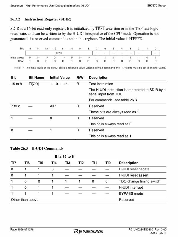
Section 26 High-Performance User Debugging Interface (H-UDI)
Page 1096 of 1278 R01UH0234EJ0300 Rev. 3.00 Jun 21, 2011
SH7670 Group
26.3.2 Instruction Register (SDIR)
SDIR is a 16-bit read-only register. It is initialized by TRST assertion or in the TAP test-logic-reset state, and can be written to by the H-UDI irrespective of the CPU mode. Operation is not guaranteed if a reserved command is set in this register. The initial value is H'EFFD.
15 14 13 12 11 10 9 8 7 6 5 4 3 2 1 0
Note: The initial value of the TI[7:0] bits is a reserved value. When setting a command, the TI[7:0] bits must be set to another value.*
1* 1* 1* 0* 1* 1* 1* 1* 1 1 1 1 1 1 0 1R R R R R R R R R R R R R R R R
Bit:
Initial value:R/W:
TI[7:0] - - - - - - - -
Bit Bit Name Initial Value R/W Description
15 to 8 TI[7:0] 11101111* R Test Instruction
The H-UDI instruction is transferred to SDIR by a serial input from TDI.
For commands, see table 26.3.
7 to 2 ⎯ All 1 R Reserved
These bits are always read as 1.
1 ⎯ 0 R Reserved
This bit is always read as 0.
0 ⎯ 1 R Reserved
This bit is always read as 1.
Table 26.3 H-UDI Commands
Bits 15 to 8
TI7 TI6 TI5 TI4 TI3 TI2 TI1 TI0 Description
0 1 1 0 — — — — H-UDI reset negate
0 1 1 1 — — — — H-UDI reset assert
1 0 0 1 1 1 0 0 TDO change timing switch
1 0 1 1 — — — — H-UDI interrupt
1 1 1 1 — — — — BYPASS mode
Other than above Reserved
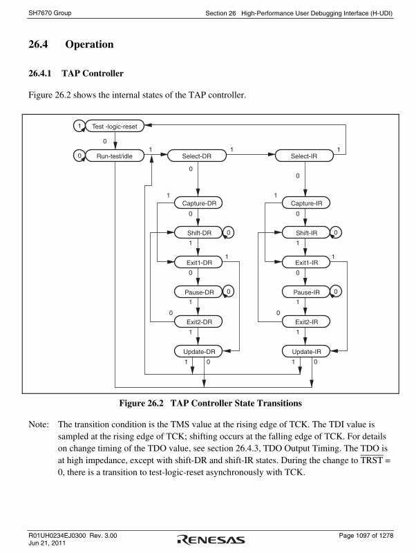
Section 26 High-Performance User Debugging Interface (H-UDI)
R01UH0234EJ0300 Rev. 3.00 Page 1097 of 1278 Jun 21, 2011
SH7670 Group
26.4 Operation
26.4.1 TAP Controller
Figure 26.2 shows the internal states of the TAP controller.
Test -logic-reset
Capture-DR
Shift-DR
Exit1-DR
Pause-DR
Exit2-DR
Update-DR
Select-DRRun-test/idle
1
0
0
0
01 1 1
1
0
0
0
1
1 1
0
1
1
1 0
Capture-IR
Shift-IR
Exit1-IR
Pause-IR
Exit2-IR
Update-IR
Select-IR
0
0
1
0
0
0
1
0
1
1
1 0
Figure 26.2 TAP Controller State Transitions
Note: The transition condition is the TMS value at the rising edge of TCK. The TDI value is sampled at the rising edge of TCK; shifting occurs at the falling edge of TCK. For details on change timing of the TDO value, see section 26.4.3, TDO Output Timing. The TDO is at high impedance, except with shift-DR and shift-IR states. During the change to TRST = 0, there is a transition to test-logic-reset asynchronously with TCK.

Section 26 High-Performance User Debugging Interface (H-UDI)
Page 1098 of 1278 R01UH0234EJ0300 Rev. 3.00 Jun 21, 2011
SH7670 Group
26.4.2 Reset Configuration
Table 26.4 Reset Configuration
ASEMD*1 RES TRST Chip State
H L L Power-on reset and H-UDI reset
H Power-on reset
H L H-UDI reset only
H Normal operation
L L L Reset hold*2
H Power-on reset
H L H-UDI reset only
H Normal operation
Notes: 1. Performs normal mode and ASE mode settings
ASEMD = H, normal mode
ASEMD = L, ASE mode 2. In ASE mode, reset hold is entered if the TRST pin is driven low while the RES pin is
negated. In this state, the CPU does not start up. When TRST is driven high, H-UDI operation is enabled, but the CPU does not start up. The reset hold state is cancelled by a power-on reset.

Section 26 High-Performance User Debugging Interface (H-UDI)
R01UH0234EJ0300 Rev. 3.00 Page 1099 of 1278 Jun 21, 2011
SH7670 Group
26.4.3 TDO Output Timing
The initial value of the TDO change timing is to perform data output from the TDO pin on the TCK falling edge. However, setting a TDO change timing switch command in SDIR via the H-UDI pin and passing the Update-IR state synchronizes the TDO change timing to the TCK rising edge. Hereafter, to synchronize the change timing of TDO to the falling edge of TCK, the TRST pin must be simultaneously asserted with the power-on reset. In a case of power-on reset by the RES pin, the sync reset is still in operation for a certain period in the LSI even after the RES pin is negated. Thus, if the TRST pin is asserted immediately after the negate of the RES pin, the TDO change timing switch command is cleared, resulting the TDO change timing synchronized with the falling edge of TCK. To prevent this, make sure to put a period of 20 times of tcyc or longer between the signal change timing of the RES and TRST pins.
TDO(initial value)
TCK
TDO(after execution of TDO change
timing switch command)
tTDOD
tTDOD
Figure 26.3 H-UDI Data Transfer Timing

Section 26 High-Performance User Debugging Interface (H-UDI)
Page 1100 of 1278 R01UH0234EJ0300 Rev. 3.00 Jun 21, 2011
SH7670 Group
26.4.4 H-UDI Reset
An H-UDI reset is executed by setting an H-UDI reset assert command in SDIR. An H-UDI reset is of the same kind as a power-on reset. An H-UDI reset is released by setting an H-UDI reset negate command. The required time between the H-UDI reset assert command and H-UDI reset negate command is the same as time for keeping the RES pin low to apply a power-on reset.
H-UDI reset assert H-UDI reset negateSDIR
Chip internal reset
CPU stateFetch the initial values of PC and SR from the exception handling vector table
Figure 26.4 H-UDI Reset
26.4.5 H-UDI Interrupt
The H-UDI interrupt function generates an interrupt by setting a command from the H-UDI in SDIR. An H-UDI interrupt is a general exception/interrupt operation, resulting in fetching the exception service routine start address from the exception handling vector table, jumping to that address, and starting program execution from that address. This interrupt request has a fixed priority level of 15.
H-UDI interrupts are accepted in sleep mode, but not in software standby mode.

Section 26 High-Performance User Debugging Interface (H-UDI)
R01UH0234EJ0300 Rev. 3.00 Page 1101 of 1278 Jun 21, 2011
SH7670 Group
26.5 Usage Notes
1. An H-UDI command, once set, will not be modified as long as another command is not set again from the H-UDI. If the same command is to be set continuously, the command must be set after a command (BYPASS mode, etc.) that does not affect chip operations is once set.
2. In software standby mode and H-UDI module standby state, all of the functions in the H-UDI cannot be used. To retain the TAP status before and after standby mode, keep TCK high before entering standby mode.
3. Regardless of whether the H-UDI is used, the TRST pin needs to be kept low at power-on to initialize the H-UDI. This can be done by treating the TRST pin as described in the emulator's manual in a board to which an emulator is to be connected, and by pulling down the TRST pin in a board to which no emulator is connected.
4. Make sure to put 20 tcyc or more between the signal change timing of the RES and TRST pins.
5. When starting the TAP controller after the negation of the TRST pin, make sure to allow 200 ns or more after the negation.
6. In a board to which an emulator is to be connected, treat the TCK, TMS, TDI, and TDO pins as described in the emulator's manual. In a board to which no emulator is connected, the TCK pin should be pulled up and the TMS, TDI, and TDO pins left open. Though TMS and TDI are input-only pins, leaving them open will not cause any problem because this LSI incorporates pull-up resistors.

Section 26 High-Performance User Debugging Interface (H-UDI)
Page 1102 of 1278 R01UH0234EJ0300 Rev. 3.00 Jun 21, 2011
SH7670 Group

Section 27 On-Chip RAM
R01UH0234EJ0300 Rev. 3.00 Page 1103 of 1278 Jun 21, 2011
SH7670 Group
Section 27 On-Chip RAM
This LSI has an on-chip RAM module which can be used to store instructions or data.
On-chip RAM operation and write access to the RAM can be enabled or disabled through the RAM enable bits and RAM write enable bits.
27.1 Features
• Pages
The on-chip RAM is divided into four pages (pages 0 to 3).
• Memory map
The on-chip RAM is located in the address spaces shown in table 27.1. Table 27.1 On-Chip RAM Address Spaces
32 Kbytes
Page Address
Page 0 H'FFF80000 to H'FFF81FFF
Page 1 H'FFF82000 to H'FFF83FFF
Page 2 H'FFF84000 to H'FFF85FFF
Page 3 H'FFF86000 to H'FFF87FFF
• Ports
Each page has two independent read and write ports and is connected to the internal bus (I bus), CPU instruction fetch bus (F bus), and CPU memory access bus (M bus). (Note that the F bus is connected only to the read ports.)
The F bus and M bus are used for access by the CPU, and the I bus is used for access by the DMAC.
• Priority
When the same page is accessed from different buses simultaneously, the access is processed according to the priority. The priority is I bus > M bus > F bus.

Section 27 On-Chip RAM
Page 1104 of 1278 R01UH0234EJ0300 Rev. 3.00 Jun 21, 2011
SH7670 Group
27.2 Usage Notes
27.2.1 Page Conflict
When the same page is accessed from different buses simultaneously, a conflict on the page occurs. Although each access is completed correctly, this kind of conflict degrades the memory access speed. Therefore, it is advisable to provide software measures to prevent such conflicts as far as possible. For example, no conflict will arise if different pages are accessed by each bus.
27.2.2 RAME and RAMWE Bits
Before disabling memory operation or write access through the RAME or RAMWE bit, be sure to read from any address and then write to the same address in each page; otherwise, the last written data in each page may not be actually written to the RAM.
// For page 0
MOV.L #H'FFF80000,R0
MOV.L @R0,R1
MOV.L R1,@R0
// For page 1
MOV.L #H'FFF82000,R0
MOV.L @R0,R1
MOV.L R1,@R0
// For page 2
MOV.L #H'FFF84000,R0
MOV.L @R0,R1
MOV.L R1,@R0
// For page 3
MOV.L #H'FFF86000,R0
MOV.L @R0,R1
MOV.L R1,@R0
Figure 27.1 Examples of Read/Write before Disabling RAM

Section 28 List of Registers
R01UH0234EJ0300 Rev. 3.00 Page 1105 of 1278 Jun 21, 2011
SH7670 Group
Section 28 List of Registers
This section gives information on the on-chip I/O registers of this LSI as follows.
1. Register Addresses (by functional module, in order of the manual's section numbers):
• Registers are described by functional module, in order of the manual's section numbers.
• Access to reserved addresses that are not described in this list of register addresses is prohibited.
• When addresses consist of 16 or 32 bits, the addresses of the MSBs are given on the assumption that big-endian mode is selected.
2. Register Bits:
• Bit configurations of the registers are described in the same order as the list of register addresses (by functional module, in order of the manual's section numbers).
• Reserved bits are indicated by "⎯" in the bit name.
• No entry in the bit-name column indicates that the whole register is allocated as a counter or for holding data.
3. Register States in Each Operating Mode:
• States of the registers are described in the same order as the list of register addresses (by functional module, in order of the manual's section numbers).
• For the initial state of each bit, refer to the description of the register in the corresponding section.
• The register states described are for basic operating modes. If there is a specific reset for an on-chip peripheral module, refer to the section on that on-chip peripheral module.
4. Cautions Required when Writing into Registers in On-Chip Peripheral Modules:
Accessing a register in an on-chip peripheral module takes at least two cycles of the peripheral module clock (Pφ) from the internal bus. When, meanwhile, writing from the CPU to an on-chip peripheral module, the CPU executes subsequent instructions without waiting for the register writing to be completed.
Here is an example involving a state transition to software standby mode for the purpose of reducing power consumption. This transition requires a SLEEP instruction to be executed after the SYBY bit of the STBCR register is set to 1. Before the execution of the SLEEP instruction, actually, it is necessary to read the STBCR register on a dummy basis. In the absence of dummy reading, the CPU executes the SLEEP instruction before the SYBY bit is set to 1, so that the state occurring after the transition will be not software standby mode, but sleep mode. Dummy-reading the STBCR register is thus required to wait until writing into the STBY bit is completed.
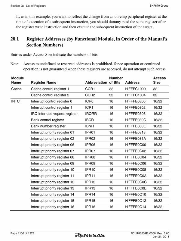
Section 28 List of Registers
Page 1106 of 1278 R01UH0234EJ0300 Rev. 3.00 Jun 21, 2011
SH7670 Group
If, as in this example, you want to reflect the change from an on-chip peripheral register at the time of execution of a subsequent instruction, you should dummy-read the same register after the register write instruction and then execute the subsequent instruction of the target.
28.1 Register Addresses (by Functional Module, in Order of the Manual's Section Numbers)
Entries under Access Size indicate the numbers of bits.
Note: Access to undefined or reserved addresses is prohibited. Since operation or continued operation is not guaranteed when these registers are accessed, do not attempt such access.
Module Name Register Name Abbreviation
Number of Bits Address
Access Size
Cache Cache control register 1 CCR1 32 H'FFFC1000 32
Cache control register 2 CCR2 32 H'FFFC1004 32
INTC Interrupt control register 0 ICR0 16 H'FFFE0800 16/32
Interrupt control register 1 ICR1 16 H'FFFE0802 16/32
IRQ interrupt request register IRQRR 16 H'FFFE0806 16/32
Bank control register IBCR 16 H'FFFE080C 16/32
Bank number register IBNR 16 H'FFFE080E 16/32
Interrupt priority register 01 IPR01 16 H'FFFE0818 16/32
Interrupt priority register 02 IPR02 16 H'FFFE081A 16/32
Interrupt priority register 06 IPR06 16 H'FFFE0C00 16/32
Interrupt priority register 07 IPR07 16 H'FFFE0C02 16/32
Interrupt priority register 08 IPR08 16 H'FFFE0C04 16/32
Interrupt priority register 09 IPR09 16 H'FFFE0C06 16/32
Interrupt priority register 10 IPR10 16 H'FFFE0C08 16/32
Interrupt priority register 11 IPR11 16 H'FFFE0C0A 16/32
Interrupt priority register 12 IPR12 16 H'FFFE0C0C 16/32
Interrupt priority register 13 IPR13 16 H'FFFE0C0E 16/32
Interrupt priority register 14 IPR14 16 H'FFFE0C10 16/32
Interrupt priority register 15 IPR15 16 H'FFFE0C12 16/32
Interrupt priority register 16 IPR16 16 H'FFFE0C14 16/32

Section 28 List of Registers
R01UH0234EJ0300 Rev. 3.00 Page 1107 of 1278 Jun 21, 2011
SH7670 Group
Module Name Register Name Abbreviation
Number of Bits Address
Access Size
BSC Common control register CMNCR 32 H'FFFC0000 32
CS0 space bus control register CS0BCR 32 H'FFFC0004 32
CS3 space bus control register CS3BCR 32 H'FFFC0010 32
CS4 space bus control register CS4BCR 32 H'FFFC0014 32
CS5 space bus control register CS5BCR 32 H'FFFC0018 32
CS6 space bus control register CS6BCR 32 H'FFFC001C 32
CS0 space wait control register CS0WCR 32 H'FFFC0028 32
CS3 space wait control register CS3WCR 32 H'FFFC0034 32
CS4 space wait control register CS4WCR 32 H'FFFC0038 32
CS5 space wait control register CS5WCR 32 H'FFFC003C 32
CS6 space wait control register CS6WCR 32 H'FFFC0040 32
SDRAM control register SDCR 32 H'FFFC004C 32
Refresh timer control/status register
RTCSR 32 H'FFFC0050 32
Refresh timer counter RTCNT 32 H'FFFC0054 32
Refresh time constant register RTCOR 32 H'FFFC0058 32
Internal bus master bus priority register
IBMPR 32 H'FFFC1818 32
DMAC DMA source address register_0 SAR_0 32 H'FFFE1000 16/32
DMA destination address register_0
DAR_0 32 H'FFFE1004 16/32
DMA transfer count register_0 DMATCR_0 32 H'FFFE1008 16/32
DMA channel control register_0 CHCR_0 32 H'FFFE100C 8/16/32
DMA source address register_1 SAR_1 32 H'FFFE1010 16/32
DMA destination address register_1
DAR_1 32 H'FFFE1014 16/32

Section 28 List of Registers
Page 1108 of 1278 R01UH0234EJ0300 Rev. 3.00 Jun 21, 2011
SH7670 Group
Module Name Register Name Abbreviation
Number of Bits Address
Access Size
DMAC DMA transfer count register_1 DMATCR_1 32 H'FFFE1018 16/32
DMA channel control register_1 CHCR_1 32 H'FFFE101C 8/16/32
DMA source address register_2 SAR_2 32 H'FFFE1020 16/32
DMA destination address register_2
DAR_2 32 H'FFFE1024 16/32
DMA transfer count register_2 DMATCR_2 32 H'FFFE1028 16/32
DMA channel control register_2 CHCR_2 32 H'FFFE102C 8/16/32
DMA source address register_3 SAR_3 32 H'FFFE1030 16/32
DMA destination address register_3
DAR_3 32 H'FFFE1034 16/32
DMA transfer count register_3 DMATCR_3 32 H'FFFE1038 16/32
DMA channel control register_3 CHCR_3 32 H'FFFE103C 8/16/32
DMA source address register_4 SAR_4 32 H'FFFE1040 16/32
DMA destination address register_4
DAR_4 32 H'FFFE1044 16/32
DMA transfer count register_4 DMATCR_4 32 H'FFFE1048 16/32
DMA channel control register_4 CHCR_4 32 H'FFFE104C 8/16/32
DMA source address register_5 SAR_5 32 H'FFFE1050 16/32
DMA destination address register_5
DAR_5 32 H'FFFE1054 16/32
DMA transfer count register_5 DMATCR_5 32 H'FFFE1058 16/32
DMA channel control register_5 CHCR_5 32 H'FFFE105C 8/16/32
DMA source address register_6 SAR_6 32 H'FFFE1060 16/32
DMA destination address register_6
DAR_6 32 H'FFFE1064 16/32
DMA transfer count register_6 DMATCR_6 32 H'FFFE1068 16/32

Section 28 List of Registers
R01UH0234EJ0300 Rev. 3.00 Page 1109 of 1278 Jun 21, 2011
SH7670 Group
Module Name Register Name Abbreviation
Number of Bits Address
Access Size
DMAC DMA channel control register_6 CHCR_6 32 H'FFFE106C 8/16/32
DMA source address register_7 SAR_7 32 H'FFFE1070 16/32
DMA destination address register_7
DAR_7 32 H'FFFE1074 16/32
DMA transfer count register_7 DMATCR_7 32 H'FFFE1078 16/32
DMA channel control register_7 CHCR_7 32 H'FFFE107C 8/16/32
DMA reload source address register_0
RSAR_0 32 H'FFFE1100 16/32
DMA reload destination address register_0
RDAR_0 32 H'FFFE1104 16/32
DMA reload transfer count register_0
RDMATCR_0 32 H'FFFE1108 16/32
DMA reload source address register_1
RSAR_1 32 H'FFFE1110 16/32
DMA reload destination address register_1
RDAR_1 32 H'FFFE1114 16/32
DMA reload transfer count register_1
RDMATCR_1 32 H'FFFE1118 16/32
DMA reload source address register_2
RSAR_2 32 H'FFFE1120 16/32
DMA reload destination address register_2
RDAR_2 32 H'FFFE1124 16/32
DMA reload transfer count register_2
RDMATCR_2 32 H'FFFE1128 16/32
DMA reload source address register_3
RSAR_3 32 H'FFFE1130 16/32
DMA reload destination address register_3
RDAR_3 32 H'FFFE1134 16/32
DMA reload transfer count register_3
RDMATCR_3 32 H'FFFE1138 16/32
DMA reload source address register_4
RSAR_4 32 H'FFFE1140 16/32
DMA reload destination address register_4
RDAR_4 32 H'FFFE1144 16/32

Section 28 List of Registers
Page 1110 of 1278 R01UH0234EJ0300 Rev. 3.00 Jun 21, 2011
SH7670 Group
Module Name Register Name Abbreviation
Number of Bits Address
Access Size
DMAC DMA reload transfer count register_4
RDMATCR_4 32 H'FFFE1148 16/32
DMA reload source address register_5
RSAR_5 32 H'FFFE1150 16/32
DMA reload destination address register_5
RDAR_5 32 H'FFFE1154 16/32
DMA reload transfer count register_5
RDMATCR_5 32 H'FFFE1158 16/32
DMA reload source address register_6
RSAR_6 32 H'FFFE1160 16/32
DMA reload destination address register_6
RDAR_6 32 H'FFFE1164 16/32
DMA reload transfer count register_6
RDMATCR_6 32 H'FFFE1168 16/32
DMA reload source address register_7
RSAR_7 32 H'FFFE1170 16/32
DMA reload destination address register_7
RDAR_7 32 H'FFFE1174 16/32
DMA reload transfer count register_7
RDMATCR_7 32 H'FFFE1178 16/32
DMA operation register DMAOR 16 H'FFFE1200 8/16
DM extension resource selector 0 DMARS0 16 H'FFFE1300 16
DM extension resource selector 1 DMARS1 16 H'FFFE1304 16
DM extension resource selector 2 DMARS2 16 H'FFFE1308 16
DM extension resource selector 3 DMARS3 16 H'FFFE130C 16
CPG Frequency control register FRQCR 16 H'FFFE0010 16
WDT Watchdog timer control/status register
WTCSR 8 H'FFFE0000 16
Watchdog timer counter WTCNT 8 H'FFFE0002 16
Watchdog reset control/status register
WRCSR 8 H'FFFE0004 16

Section 28 List of Registers
R01UH0234EJ0300 Rev. 3.00 Page 1111 of 1278 Jun 21, 2011
SH7670 Group
Module Name Register Name Abbreviation
Number of Bits Address
Access Size
Standby control register STBCR 8 H'FFFE0014 8 Power-down mode Standby control register 2 STBCR2 8 H'FFFE0018 8
System control register 1 SYSCR1 8 H'FFFE0402 8
System control register 2 SYSCR2 8 H'FFFE0404 8
Standby control register 3 STBCR3 8 H'FFFE0408 8
Standby control register 4 STBCR4 8 H'FFFE040C 8
System control register 3 SYSCR3 8 H'FFFE0418 8
EtherC EtherC mode register ECMR 32 H'FFFC2160 32
EtherC status register ECSR 32 H'FFFC2164 32
EtherC interrupt enable register ECSIPR 32 H'FFFC2168 32
PHY section interface register PIR 32 H'FFFC216C 32
MAC higher-order address register
MAHR 32 H'FFFC2170 32
MAC lower-order address register
MALR 32 H'FFFC2174 32
Upper receive frame length limit register
RFLR 32 H'FFFC2178 32
PHY section status register PSR 32 H'FFFC217C 32
Transmit retry counter register TROCR 32 H'FFFC2180 32
Delay collision detection counter register
CDCR 32 H'FFFC2184 32
Carrier loss counter register LCCR 32 H'FFFC2188 32
Undetected carrier counter register
CNDCR 32 H'FFFC218C 32
CRC error frame reception counter register
CEFCR 32 H'FFFC2194 32
Frame reception error counter register
FRECR 32 H'FFFC2198 32

Section 28 List of Registers
Page 1112 of 1278 R01UH0234EJ0300 Rev. 3.00 Jun 21, 2011
SH7670 Group
Module Name Register Name Abbreviation
Number of Bits Address
Access Size
EtherC Lower than 64 bytes frame reception counter register
TSFRCR 32 H'FFFC219C 32
Excessive bytes frame reception counter register
TLFRCR 32 H'FFFC21A0 32
Fractional bits frame reception counter register
RFCR 32 H'FFFC21A4 32
Multicast address frame reception counter register
MAFCR 32 H'FFFC21A8 32
IPG setting register IPGR 32 H'FFFC21B4 32
Automatic PAUSE frame setting register
APR 32 H'FFFC21B8 32
Manual PAUSE frame setting register
MPR 32 H'FFFC21BC 32
Automatic PAUSE frame resend count setting register
TPAUSER 32 H'FFFC21C4 32
E-DMAC E-DMAC mode register EDMR 32 H'FFFC2000 32
E-DMAC send request register EDTRR 32 H'FFFC2004 32
E-DMAC receive request register
EDRRR 32 H'FFFC2008 32
Transmit descriptor list's starting address register
TDLAR 32 H'FFFC200C 32
Receive descriptor list's starting address register
RDLAR 32 H'FFFC2010 32
EtherC/E-DMAC status register EESR 32 H'FFFC2014 32
EtherC/E-DMAC status interrupt enable register
EESIPR 32 H'FFFC2018 32
Transmit /receive status copying register
TRSCER 32 H'FFFC201C 32
Missed frames counter register RMFCR 32 H'FFFC2020 32
Transmit FIFO threshold value register
TFTR 32 H'FFFC2024 32
FIFO capacity register FDR 32 H'FFFC2028 32
Receive method control register
RMCR 32 H'FFFC202C 32

Section 28 List of Registers
R01UH0234EJ0300 Rev. 3.00 Page 1113 of 1278 Jun 21, 2011
SH7670 Group
Module Name Register Name Abbreviation
Number of Bits Address
Access Size
E-DMAC E-DMAC operation control register
EDOCR 32 H'FFFC2030 32
Flow control start FIFO threshold value register
FCFTR 32 H'FFFC2034 32
Receive data padding setting register
RPADIR 32 H'FFFC2038 32
Transmit interrupt setting register
TRIMD 32 H'FFFC203C 32
Receive buffer write address register
RBWAR 32 H'FFFC2040 32
Receive descriptor fetch address register
RDFAR 32 H'FFFC2044 32
Transmit buffer read address register
TBRAR 32 H'FFFC204C 32
Transmit descriptor fetch address register
TDFAR 32 H'FFFC2050 32
Checksum mode register CSMR 32 H'FFFC20E4 32
Checksum skipped bytes monitor register
CSSBM 32 H'FFFC20E8 32
Checksum monitor register CSSMR 32 H'FFFC20EC 32
A-DMAC Channel 0 processing control register
C0C 32 H'FFFC2440 32
Channel 0 processing mode register
C0M 32 H'FFFC2444 32
Channel 0 processing interrupt request register
C0I 32 H'FFFC2448 32
Channel 0 processing descriptor starting address register
C0DSA 32 H'FFFC247C 32
Channel 0 processing descriptor current address register
C0DCA 32 H'FFFC2480 32
Channel 0 processing descriptor 0 register
C0D0 32 H'FFFC2484 32
Channel 0 processing descriptor 1 register
C0D1 32 H'FFFC2488 32
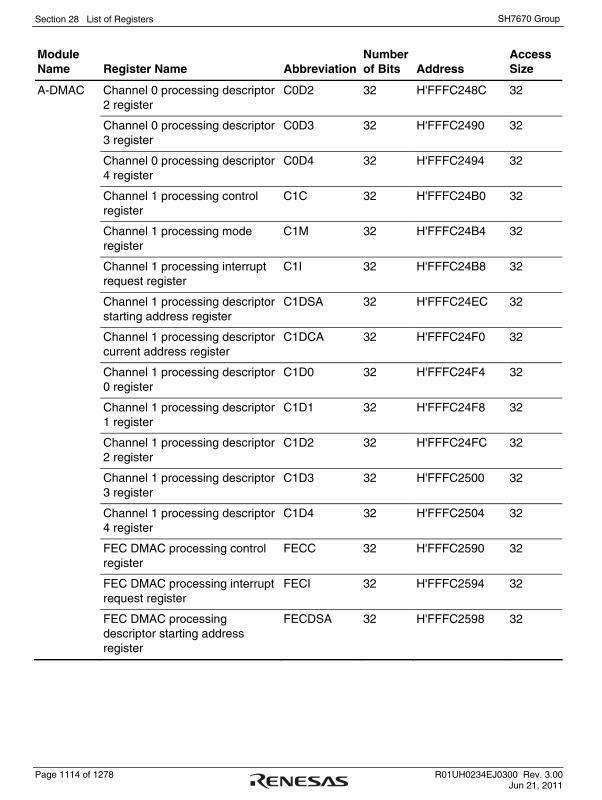
Section 28 List of Registers
Page 1114 of 1278 R01UH0234EJ0300 Rev. 3.00 Jun 21, 2011
SH7670 Group
Module Name Register Name Abbreviation
Number of Bits Address
Access Size
A-DMAC Channel 0 processing descriptor 2 register
C0D2 32 H'FFFC248C 32
Channel 0 processing descriptor 3 register
C0D3 32 H'FFFC2490 32
Channel 0 processing descriptor 4 register
C0D4 32 H'FFFC2494 32
Channel 1 processing control register
C1C 32 H'FFFC24B0 32
Channel 1 processing mode register
C1M 32 H'FFFC24B4 32
Channel 1 processing interrupt request register
C1I 32 H'FFFC24B8 32
Channel 1 processing descriptor starting address register
C1DSA 32 H'FFFC24EC 32
Channel 1 processing descriptor current address register
C1DCA 32 H'FFFC24F0 32
Channel 1 processing descriptor 0 register
C1D0 32 H'FFFC24F4 32
Channel 1 processing descriptor 1 register
C1D1 32 H'FFFC24F8 32
Channel 1 processing descriptor 2 register
C1D2 32 H'FFFC24FC 32
Channel 1 processing descriptor 3 register
C1D3 32 H'FFFC2500 32
Channel 1 processing descriptor 4 register
C1D4 32 H'FFFC2504 32
FEC DMAC processing control register
FECC 32 H'FFFC2590 32
FEC DMAC processing interrupt request register
FECI 32 H'FFFC2594 32
FEC DMAC processing descriptor starting address register
FECDSA 32 H'FFFC2598 32
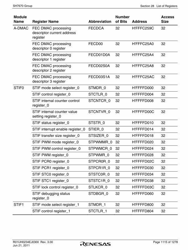
Section 28 List of Registers
R01UH0234EJ0300 Rev. 3.00 Page 1115 of 1278 Jun 21, 2011
SH7670 Group
Module Name Register Name Abbreviation
Number of Bits Address
Access Size
A-DMAC FEC DMAC processing descriptor current address register
FECDCA 32 H'FFFC259C 32
FEC DMAC processing descriptor 0 register
FECD00 32 H'FFFC25A0 32
FEC DMAC processing descriptor 1 register
FECD01D0A 32 H'FFFC25A4 32
FEC DMAC processing descriptor 2 register
FECD02S0A 32 H'FFFC25A8 32
FEC DMAC processing descriptor 3 register
FECD03S1A 32 H'FFFC25AC 32
STIF0 STIF mode select register_0 STMDR_0 32 H'FFFFD000 32
STIF control register_0 STCTLR_0 32 H'FFFFD004 32
STIF internal counter control register_0
STCNTCR_0 32 H'FFFFD008 32
STIF internal counter value setting register_0
STCNTVR_0 32 H'FFFFD00C 32
STIF status register_0 STSTR_0 32 H'FFFFD010 32
STIF interrupt enable register_0 STIER_0 32 H'FFFFD014 32
STIF transfer size register_0 STSIZER_0 32 H'FFFFD018 32
STIF PWM mode register_0 STPWMMR_0 32 H'FFFFD020 32
STIF PWM control register_0 STPWMCR_0 32 H'FFFFD024 32
STIF PWM register_0 STPWMR_0 32 H'FFFFD028 32
STIF PCR0 register_0 STPCR0R_0 32 H'FFFFD02C 32
STIF PCR1 register_0 STPCR1R_0 32 H'FFFFD030 32
STIF STC0 register_0 STSTC0R_0 32 H'FFFFD034 32
STIF STC1 register_0 STSTC1R_0 32 H'FFFFD038 32
STIF lock control register_0 STLKCR_0 32 H'FFFFD03C 32
STIF debugging status register_0
STDBGR_0 32 H'FFFFD060 32
STIF1 STIF mode select register_1 STMDR_1 32 H'FFFFD800 32
STIF control register_1 STCTLR_1 32 H'FFFFD804 32

Section 28 List of Registers
Page 1116 of 1278 R01UH0234EJ0300 Rev. 3.00 Jun 21, 2011
SH7670 Group
Module Name Register Name Abbreviation
Number of Bits Address
Access Size
STIF1 STIF internal counter control register_1
STCNTCR_1 32 H'FFFFD808 32
STIF internal counter value setting register_1
STCNTVR_1 32 H'FFFFD80C 32
STIF status register_1 STSTR_1 32 H'FFFFD810 32
STIF interrupt enable register_1 STIER_1 32 H'FFFFD814 32
STIF transfer size register_1 STSIZER_1 32 H'FFFFD818 32
STIF PWM mode register_1 STPWMMR_1 32 H'FFFFD820 32
STIF PWM control register_1 STPWMCR_1 32 H'FFFFD824 32
STIF PWM register_1 STPWMR_1 32 H'FFFFD828 32
STIF PCR0 register_1 STPCR0R_1 32 H'FFFFD82C 32
STIF PCR1 register_1 STPCR1R_1 32 H'FFFFD830 32
STIF STC0 register_1 STSTC0R_1 32 H'FFFFD834 32
STIF STC1 register_1 STSTC1R_1 32 H'FFFFD838 32
STIF lock control register_1 STLKCR_1 32 H'FFFFD83C 32
STIF debugging status register_1 STDBGR_1 32 H'FFFFD860 32
SSI SSI clock selection register_0 SCSR_0 16 H'FFFF0000 16
SSI clock selection register_1 SCSR_1 16 H'FFFF0800 16
Control register_0 SSICR_0 32 H'FFFFC000 32
Status register_0 SSISR_0 32 H'FFFFC004 32
Transmit data register_0 SSITDR_0 32 H'FFFFC008 32
Receive data register_0 SSIRDR_0 32 H'FFFFC00C 32
Control register_1 SSICR_1 32 H'FFFFC800 32
Status register_1 SSISR_1 32 H'FFFFC804 32
Transmit data register_1 SSITDR_1 32 H'FFFFC808 32
Receive data register_1 SSIRDR_1 32 H'FFFFC80C 32
USB D0FIFO bus wait setting register D0FWAIT 16 H'FFFC1C0C 16
D1FIFO bus wait setting register D1FWAIT 16 H'FFFC1C0E 16

Section 28 List of Registers
R01UH0234EJ0300 Rev. 3.00 Page 1117 of 1278 Jun 21, 2011
SH7670 Group
Module Name Register Name Abbreviation
Number of Bits Address
Access Size
USB D0FIFO port register D0FIFO 32 H'FFFC1C14 32
D1FIFO port register D1FIFO 32 H'FFFC1C18 32
System configuration control register
SYSCFG 16 H'FFFFF800 16
CPU bus wait setting register BUSWAIT 16 H'FFFFF802 16
System configuration status register
SYSSTS 16 H'FFFFF804 16
Device control register DVSTCTR 16 H'FFFFF808 16
Test mode register TESTMODE 16 H'FFFFF80C 16
D0FIFO bus configuration register D0FBCFG 16 H'FFFFF810 16
D1FIFO bus configuration register D1FBCFG 16 H'FFFFF812 16
CFIFO port register CFIFO 32 H'FFFFF814 8/16/32
CFIFO port selection register CFIFOSEL 16 H'FFFFF820 16
CFIFO port control register CFIFOCTR 16 H'FFFFF822 16
D0CFIFO port selection register D0FIFOSEL 16 H'FFFFF828 16
D0FIFO port control register D0FIFOCTR 16 H'FFFFF82A 16
D1CFIFO port selection register D1FIFOSEL 16 H'FFFFF82C 16
D1FIFO port control register D1FIFOCTR 16 H'FFFFF82E 16
Interrupt enable register 0 INTENB0 16 H'FFFFF830 16
Interrupt enable register 1 INTENB1 16 H'FFFFF832 16
BRDY interrupt enable register BRDYENB 16 H'FFFFF836 16
NRDY interrupt enable register NRDYENB 16 H'FFFFF838 16
BEMP interrupt enable register BEMPENB 16 H'FFFFF83A 16
SOF output configuration register SOFCFG 16 H'FFFFF83C 16
Interrupt status register 0 INTSTS0 16 H'FFFFF840 16
Interrupt status register 1 INTSTS1 16 H'FFFFF842 16
BRDY interrupt status register BRDYSTS 16 H'FFFFF846 16

Section 28 List of Registers
Page 1118 of 1278 R01UH0234EJ0300 Rev. 3.00 Jun 21, 2011
SH7670 Group
Module Name Register Name Abbreviation
Number of Bits Address
Access Size
USB NRDY interrupt status register NRDYSTS 16 H'FFFFF848 16
BEMP interrupt status register BEMPSTS 16 H'FFFFF84A 16
Frame number register FRMNUM 16 H'FFFFF84C 16
μ frame number register UFRMNUM 16 H'FFFFF84E 16
USB address register USBADDR 16 H'FFFFF850 16
USB request type register USBREQ 16 H'FFFFF854 16
USB request value register USBVAL 16 H'FFFFF856 16
USB request index register USBINDX 16 H'FFFFF858 16
USB request length register USBLENG 16 H'FFFFF85A 16
DCP configuration register DCPCFG 16 H'FFFFF85C 16
DCP maximum packet size register
DCPMAXP 16 H'FFFFF85E 16
DCP control register DCPCTR 16 H'FFFFF860 16
Pipe window selection register PIPESEL 16 H'FFFFF864 16
Pipe configuration register PIPECFG 16 H'FFFFF868 16
Pipe buffer register PIPEBUF 16 H'FFFFF86A 16
Pipe maximum packet size register
PIPEMAXP 16 H'FFFFF86C 16
Pipe cycle control register PIPEPERI 16 H'FFFFF86E 16
PIPE1 control register PIPE1CTR 16 H'FFFFF870 16
PIPE2 control register PIPE2CTR 16 H'FFFFF872 16
PIPE3 control register PIPE3CTR 16 H'FFFFF874 16
PIPE4 control register PIPE4CTR 16 H'FFFFF876 16
PIPE5 control register PIPE5CTR 16 H'FFFFF878 16
PIPE6 control register PIPE6CTR 16 H'FFFFF87A 16
PIPE7 control register PIPE7CTR 16 H'FFFFF87C 16
PIPE8 control register PIPE8CTR 16 H'FFFFF87E 16
PIPE9 control register PIPE9CTR 16 H'FFFFF880 16
PIPE1 transaction counter enable register
PIPE1TRE 16 H'FFFFF890 16

Section 28 List of Registers
R01UH0234EJ0300 Rev. 3.00 Page 1119 of 1278 Jun 21, 2011
SH7670 Group
Module Name Register Name Abbreviation
Number of Bits Address
Access Size
USB PIPE1 transaction counter register
PIPE1TRN 16 H'FFFFF892 16
PIPE2 transaction counter enable register
PIPE2TRE 16 H'FFFFF894 16
PIPE2 transaction counter register
PIPE2TRN 16 H'FFFFF896 16
PIPE3 transaction counter enable register
PIPE3TRE 16 H'FFFFF898 16
PIPE3 transaction counter register
PIPE3TRN 16 H'FFFFF89A 16
PIPE4 transaction counter enable register
PIPE4TRE 16 H'FFFFF89C 16
PIPE4 transaction counter register
PIPE4TRN 16 H'FFFFF89E 16
PIPE5 transaction counter enable register
PIPE5TRE 16 H'FFFFF8A0 16
PIPE5 transaction counter register
PIPE5TRN 16 H'FFFFF8A2 16
Device address 0 configuration register
DEVADD0 16 H'FFFFF8D0 16
Device address 1 configuration register
DEVADD1 16 H'FFFFF8D2 16
Device address 2 configuration register
DEVADD2 16 H'FFFFF8D4 16
Device address 3 configuration register
DEVADD3 16 H'FFFFF8D6 16
Device address 4 configuration register
DEVADD4 16 H'FFFFF8D8 16
Device address 5 configuration register
DEVADD5 16 H'FFFFF8DA 16
Device address 6 configuration register
DEVADD6 16 H'FFFFF8DC 16
Device address 7 configuration register
DEVADD7 16 H'FFFFF8DE 16
Device address 8 configuration register
DEVADD8 16 H'FFFFF8E0 16

Section 28 List of Registers
Page 1120 of 1278 R01UH0234EJ0300 Rev. 3.00 Jun 21, 2011
SH7670 Group
Module Name Register Name Abbreviation
Number of Bits Address
Access Size
USB Device address 9 configuration register
DEVADD9 16 H'FFFFF8E2 16
Device address A configuration register
DEVADDA 16 H'FFFFF8E4 16
IIC3 I2C bus control register 1_0 ICCR1_0 8 H'FFFEE000 8
I2C bus control register 2_0 ICCR2_0 8 H'FFFEE001 8
I2C bus mode register_0 ICMR_0 8 H'FFFEE002 8
I2C bus interrupt enable register_0
ICIER_0 8 H'FFFEE003 8
I2C bus status register_0 ICSR_0 8 H'FFFEE004 8
Slave address register_0 SAR_0 8 H'FFFEE005 8
I2C bus transmit data register_0 ICDRT_0 8 H'FFFEE006 8
I2C bus receive data register_0 ICDRR_0 8 H'FFFEE007 8
NF2CYC register_0 NF2CYC_0 8 H'FFFEE008 8
HIF HIF index register HIFIDX 32 H'FFFFE000 32
HIF general status register HIFGSR 32 H'FFFFE004 32
HIF status/control register HIFSCR 32 H'FFFFE008 32
HIF memory control register HIFMCR 32 H'FFFFE00C 32
HIF internal interrupt control register
HIFIICR 32 H'FFFFE010 32
HIF external interrupt control register
HIFEICR 32 H'FFFFE014 32
HIF address register HIFADR 32 H'FFFFE018 32
HIF data register HIFDATA 32 H'FFFFE01C 32
HIF DREQ trigger register HIFDTR 32 H'FFFFE020 32
HIF bank interrupt control register
HIFBICR 32 H'FFFFE024 32
HIF boot control register HIFBCR 32 H'FFFFE040 32
CMT Compare match timer start register
CMSTR 16 H'FFFEC000 16
Compare match timer control/status register_0
CMCSR_0 16 H'FFFEC002 16
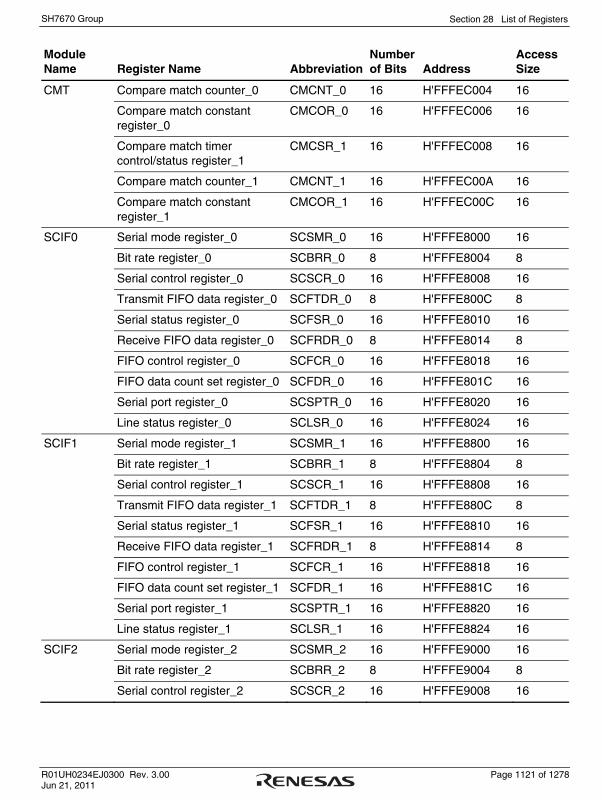
Section 28 List of Registers
R01UH0234EJ0300 Rev. 3.00 Page 1121 of 1278 Jun 21, 2011
SH7670 Group
Module Name Register Name Abbreviation
Number of Bits Address
Access Size
CMT Compare match counter_0 CMCNT_0 16 H'FFFEC004 16
Compare match constant register_0
CMCOR_0 16 H'FFFEC006 16
Compare match timer control/status register_1
CMCSR_1 16 H'FFFEC008 16
Compare match counter_1 CMCNT_1 16 H'FFFEC00A 16
Compare match constant register_1
CMCOR_1 16 H'FFFEC00C 16
SCIF0 Serial mode register_0 SCSMR_0 16 H'FFFE8000 16
Bit rate register_0 SCBRR_0 8 H'FFFE8004 8
Serial control register_0 SCSCR_0 16 H'FFFE8008 16
Transmit FIFO data register_0 SCFTDR_0 8 H'FFFE800C 8
Serial status register_0 SCFSR_0 16 H'FFFE8010 16
Receive FIFO data register_0 SCFRDR_0 8 H'FFFE8014 8
FIFO control register_0 SCFCR_0 16 H'FFFE8018 16
FIFO data count set register_0 SCFDR_0 16 H'FFFE801C 16
Serial port register_0 SCSPTR_0 16 H'FFFE8020 16
Line status register_0 SCLSR_0 16 H'FFFE8024 16
SCIF1 Serial mode register_1 SCSMR_1 16 H'FFFE8800 16
Bit rate register_1 SCBRR_1 8 H'FFFE8804 8
Serial control register_1 SCSCR_1 16 H'FFFE8808 16
Transmit FIFO data register_1 SCFTDR_1 8 H'FFFE880C 8
Serial status register_1 SCFSR_1 16 H'FFFE8810 16
Receive FIFO data register_1 SCFRDR_1 8 H'FFFE8814 8
FIFO control register_1 SCFCR_1 16 H'FFFE8818 16
FIFO data count set register_1 SCFDR_1 16 H'FFFE881C 16
Serial port register_1 SCSPTR_1 16 H'FFFE8820 16
Line status register_1 SCLSR_1 16 H'FFFE8824 16
SCIF2 Serial mode register_2 SCSMR_2 16 H'FFFE9000 16
Bit rate register_2 SCBRR_2 8 H'FFFE9004 8
Serial control register_2 SCSCR_2 16 H'FFFE9008 16

Section 28 List of Registers
Page 1122 of 1278 R01UH0234EJ0300 Rev. 3.00 Jun 21, 2011
SH7670 Group
Module Name Register Name Abbreviation
Number of Bits Address
Access Size
SCIF2 Transmit FIFO data register_2 SCFTDR_2 8 H'FFFE900C 8
Serial status register_2 SCFSR_2 16 H'FFFE9010 16
Receive FIFO data register_2 SCFRDR_2 8 H'FFFE9014 8
FIFO control register_2 SCFCR_2 16 H'FFFE9018 16
FIFO data count set register_2 SCFDR_2 16 H'FFFE901C 16
Serial port register_2 SCSPTR_2 16 H'FFFE9020 16
Line status register_2 SCLSR_2 16 H'FFFE9024 16
I/O Port A data register H PADRH 16 H'FFFE3800 8/16
Port A IO register H PAIORH 16 H'FFFE3804 8/16
Port A control register H2 PACRH2 16 H'FFFE3808 8/16
Port A control register H1 PACRH1 16 H'FFFE380A 8/16
Port B data register L PBDRL 16 H'FFFE3882 8/16
Port B IO register L PBIORL 16 H'FFFE3886 8/16
Port B control register L1 PBCRL1 16 H'FFFE388E 8/16
Port C data register H PCDRH 16 H'FFFE3900 8/16
Port C data register L PCDRL 16 H'FFFE3902 8/16
Port C IO register H PCIORH 16 H'FFFE3904 8/16
Port C IO register L PCIORL 16 H'FFFE3906 8/16
Port C control register H1 PCCRH1 16 H'FFFE390A 8/16
Port C control register L2 PCCRL2 16 H'FFFE390C 8/16
Port C control register L1 PCCRL1 16 H'FFFE390E 8/16
Port D data register L PDDRL 16 H'FFFE3982 8/16
Port D IO register L PDIORL 16 H'FFFE3986 8/16
Port D control register L1 PDCRL1 16 H'FFFE398E 8/16
Port E data register L PEDRL 16 H'FFFE3A02 8/16
Port E IO register L PEIORL 16 H'FFFE3A06 8/16
Port E control register L2 PECRL2 16 H'FFFE3A0C 8/16
Port E control register L1 PECRL1 16 H'FFFE3A0E 8/16
Port F data register L PFDRL 16 H'FFFE3A82 8/16
Port F IO register L PFIORL 16 H'FFFE3A86 8/16

Section 28 List of Registers
R01UH0234EJ0300 Rev. 3.00 Page 1123 of 1278 Jun 21, 2011
SH7670 Group
Module Name Register Name Abbreviation
Number of Bits Address
Access Size
I/O Port F control register L2 PFCRL2 16 H'FFFE3A8C 8/16
Port F control register L1 PFCRL1 16 H'FFFE3A8E 8/16
Port G data register H PGDRH 16 H'FFFE3B00 8/16
Port G data register L PGDRL 16 H'FFFE3B02 8/16
Port G IO register H PGIORH 16 H'FFFE3B04 8/16
Port G IO register L PGIORL 16 H'FFFE3B06 8/16
Port G control register H2 PGCRH2 16 H'FFFE3B0A 8/16
Port G control register L2 PGCRL2 16 H'FFFE3B0C 8/16
Port G control register L1 PGCRL1 16 H'FFFE3B0E 8/16
UBC Break address register_0 BAR_0 32 H'FFFC0400 32
Break address mask register_0 BAMR_0 32 H'FFFC0404 32
Break data register_0 BDR_0 32 H'FFFC0408 32
Break data mask register_0 BDMR_0 32 H'FFFC040C 32
Break address register_1 BAR_1 32 H'FFFC0410 32
Break address mask register_1 BAMR_1 32 H'FFFC0414 32
Break data register_1 BDR_1 32 H'FFFC0418 32
Break data mask register_1 BDMR_1 32 H'FFFC041C 32
Break bus cycle register_0 BBR_0 16 H'FFFC04A0 16
Break bus cycle register_1 BBR_1 16 H'FFFC04B0 16
Break control register BRCR 32 H'FFFC04C0 32
H-UDI Instruction register SDIR 16 H'FFFE2000 16
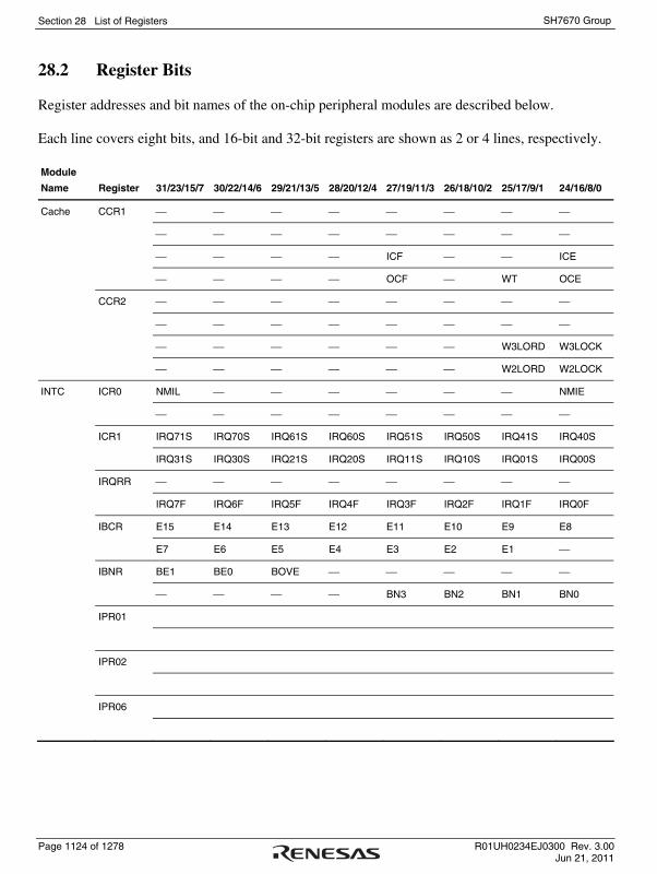
Section 28 List of Registers
Page 1124 of 1278 R01UH0234EJ0300 Rev. 3.00 Jun 21, 2011
SH7670 Group
28.2 Register Bits
Register addresses and bit names of the on-chip peripheral modules are described below.
Each line covers eight bits, and 16-bit and 32-bit registers are shown as 2 or 4 lines, respectively.
Module
Name Register 31/23/15/7 30/22/14/6 29/21/13/5 28/20/12/4 27/19/11/3 26/18/10/2 25/17/9/1 24/16/8/0
Cache CCR1 ⎯ ⎯ ⎯ ⎯ ⎯ ⎯ ⎯ ⎯
⎯ ⎯ ⎯ ⎯ ⎯ ⎯ ⎯ ⎯
⎯ ⎯ ⎯ ⎯ ICF ⎯ ⎯ ICE
⎯ ⎯ ⎯ ⎯ OCF ⎯ WT OCE
CCR2 ⎯ ⎯ ⎯ ⎯ ⎯ ⎯ ⎯ ⎯
⎯ ⎯ ⎯ ⎯ ⎯ ⎯ ⎯ ⎯
⎯ ⎯ ⎯ ⎯ ⎯ ⎯ W3LORD W3LOCK
⎯ ⎯ ⎯ ⎯ ⎯ ⎯ W2LORD W2LOCK
INTC ICR0 NMIL ⎯ ⎯ ⎯ ⎯ ⎯ ⎯ NMIE
⎯ ⎯ ⎯ ⎯ ⎯ ⎯ ⎯ ⎯
ICR1 IRQ71S IRQ70S IRQ61S IRQ60S IRQ51S IRQ50S IRQ41S IRQ40S
IRQ31S IRQ30S IRQ21S IRQ20S IRQ11S IRQ10S IRQ01S IRQ00S
IRQRR ⎯ ⎯ ⎯ ⎯ ⎯ ⎯ ⎯ ⎯
IRQ7F IRQ6F IRQ5F IRQ4F IRQ3F IRQ2F IRQ1F IRQ0F
IBCR E15 E14 E13 E12 E11 E10 E9 E8
E7 E6 E5 E4 E3 E2 E1 ⎯
IBNR BE1 BE0 BOVE ⎯ ⎯ ⎯ ⎯ ⎯
⎯ ⎯ ⎯ ⎯ BN3 BN2 BN1 BN0
IPR01
IPR02
IPR06

Section 28 List of Registers
R01UH0234EJ0300 Rev. 3.00 Page 1125 of 1278 Jun 21, 2011
SH7670 Group
Module
Name Register 31/23/15/7 30/22/14/6 29/21/13/5 28/20/12/4 27/19/11/3 26/18/10/2 25/17/9/1 24/16/8/0
INTC IPR07
IPR08
IPR09
IPR10
IPR11
IPR12
IPR13
IPR14
IPR15
IPR16
BSC CMNCR ⎯ ⎯ ⎯ ⎯ ⎯ ⎯ ⎯ ⎯
⎯ ⎯ ⎯ ⎯ ⎯ ⎯ ⎯ ⎯
⎯ ⎯ ⎯ ⎯ ⎯ ⎯ ⎯ DMAIW2
DMAIW1 DMAIW0 DMAIWA ⎯ ⎯ ⎯ HIZMEM HIZCNT
CS0BCR ⎯ IWW2 IWW1 IWW0 IWRWD2 IWRWD1 IWRWD0 IWRWS2
IWRWS1 IWRWS0 IWRRD2 IWRRD1 IWRRD0 IWRRS2 IWRRS1 IWRRS0
⎯ TYPE2 TYPE1 TYPE0 ENDIAN BSZ1 BSZ0 ⎯
⎯ ⎯ ⎯ ⎯ ⎯ ⎯ ⎯ ⎯
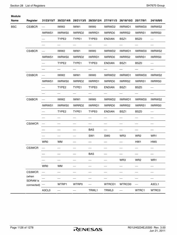
Section 28 List of Registers
Page 1126 of 1278 R01UH0234EJ0300 Rev. 3.00 Jun 21, 2011
SH7670 Group
Module
Name Register 31/23/15/7 30/22/14/6 29/21/13/5 28/20/12/4 27/19/11/3 26/18/10/2 25/17/9/1 24/16/8/0
BSC CS3BCR ⎯ IWW2 IWW1 IWW0 IWRWD2 IWRWD1 IWRWD0 IWRWS2
IWRWS1 IWRWS0 IWRRD2 IWRRD1 IWRRD0 IWRRS2 IWRRS1 IWRRS0
⎯ TYPE2 TYPE1 TYPE0 ENDIAN BSZ1 BSZ0 ⎯
⎯ ⎯ ⎯ ⎯ ⎯ ⎯ ⎯ ⎯
CS4BCR ⎯ IWW2 IWW1 IWW0 IWRWD2 IWRWD1 IWRWD0 IWRWS2
IWRWS1 IWRWS0 IWRRD2 IWRRD1 IWRRD0 IWRRS2 IWRRS1 IWRRS0
⎯ TYPE2 TYPE1 TYPE0 ENDIAN BSZ1 BSZ0 ⎯
⎯ ⎯ ⎯ ⎯ ⎯ ⎯ ⎯ ⎯
CS5BCR ⎯ IWW2 IWW1 IWW0 IWRWD2 IWRWD1 IWRWD0 IWRWS2
IWRWS1 IWRWS0 IWRRD2 IWRRD1 IWRRD0 IWRRS2 IWRRS1 IWRRS0
⎯ TYPE2 TYPE1 TYPE0 ENDIAN BSZ1 BSZ0 ⎯
⎯ ⎯ ⎯ ⎯ ⎯ ⎯ ⎯ ⎯
CS6BCR ⎯ IWW2 IWW1 IWW0 IWRWD2 IWRWD1 IWRWD0 IWRWS2
IWRWS1 IWRWS0 IWRRD2 IWRRD1 IWRRD0 IWRRS2 IWRRS1 IWRRS0
⎯ TYPE2 TYPE1 TYPE0 ENDIAN BSZ1 BSZ0 ⎯
⎯ ⎯ ⎯ ⎯ ⎯ ⎯ ⎯ ⎯
CS0WCR ⎯ ⎯ ⎯ ⎯ ⎯ ⎯ ⎯ ⎯
⎯ ⎯ ⎯ BAS ⎯ ⎯ ⎯ ⎯
⎯ ⎯ ⎯ SW1 SW0 WR3 WR2 WR1
WR0 WM ⎯ ⎯ ⎯ ⎯ HW1 HW0
CS3WCR ⎯ ⎯ ⎯ ⎯ ⎯ ⎯ ⎯ ⎯
⎯ ⎯ ⎯ BAS ⎯ ⎯ ⎯ ⎯
⎯ ⎯ ⎯ ⎯ ⎯ WR3 WR2 WR1
WR0 WM ⎯ ⎯ ⎯ ⎯ ⎯ ⎯
⎯ ⎯ ⎯ ⎯ ⎯ ⎯ ⎯ ⎯
⎯ ⎯ ⎯ ⎯ ⎯ ⎯ ⎯ ⎯
⎯ WTRP1 WTRP0 ⎯ WTRCD1 WTRCD0 ⎯ A3CL1
CS3WCR
(when
SDRAM is
connected)
A3CL0 ⎯ ⎯ TRWL1 TRWL0 ⎯ WTRC1 WTRC0
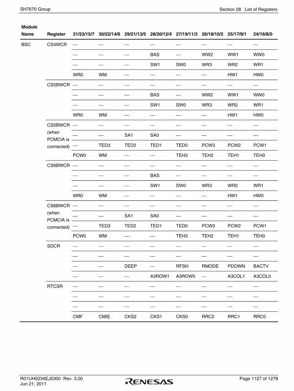
Section 28 List of Registers
R01UH0234EJ0300 Rev. 3.00 Page 1127 of 1278 Jun 21, 2011
SH7670 Group
Module
Name Register 31/23/15/7 30/22/14/6 29/21/13/5 28/20/12/4 27/19/11/3 26/18/10/2 25/17/9/1 24/16/8/0
BSC CS4WCR ⎯ ⎯ ⎯ ⎯ ⎯ ⎯ ⎯ ⎯
⎯ ⎯ ⎯ BAS ⎯ WW2 WW1 WW0
⎯ ⎯ ⎯ SW1 SW0 WR3 WR2 WR1
WR0 WM ⎯ ⎯ ⎯ ⎯ HW1 HW0
CS5BWCR ⎯ ⎯ ⎯ ⎯ ⎯ ⎯ ⎯ ⎯
⎯ ⎯ ⎯ BAS ⎯ WW2 WW1 WW0
⎯ ⎯ ⎯ SW1 SW0 WR3 WR2 WR1
WR0 WM ⎯ ⎯ ⎯ ⎯ HW1 HW0
⎯ ⎯ ⎯ ⎯ ⎯ ⎯ ⎯ ⎯
⎯ ⎯ SA1 SA0 ⎯ ⎯ ⎯ ⎯
⎯ TED3 TED2 TED1 TED0 PCW3 PCW2 PCW1
CS5BWCR
(when
PCMCIA is
connected)
PCW0 WM ⎯ ⎯ TEH3 TEH2 TEH1 TEH0
CS6BWCR ⎯ ⎯ ⎯ ⎯ ⎯ ⎯ ⎯ ⎯
⎯ ⎯ ⎯ BAS ⎯ ⎯ ⎯ ⎯
⎯ ⎯ ⎯ SW1 SW0 WR3 WR2 WR1
WR0 WM ⎯ ⎯ ⎯ ⎯ HW1 HW0
⎯ ⎯ ⎯ ⎯ ⎯ ⎯ ⎯ ⎯
⎯ ⎯ SA1 SA0 ⎯ ⎯ ⎯ ⎯
⎯ TED3 TED2 TED1 TED0 PCW3 PCW2 PCW1
CS6BWCR
(when
PCMCIA is
connected)
PCW0 WM ⎯ ⎯ TEH3 TEH2 TEH1 TEH0
SDCR ⎯ ⎯ ⎯ ⎯ ⎯ ⎯ ⎯ ⎯
⎯ ⎯ ⎯ ⎯ ⎯ ⎯ ⎯ ⎯
⎯ ⎯ DEEP ⎯ RFSH RMODE PDOWN BACTV
⎯ ⎯ ⎯ A3ROW1 A3ROW0 ⎯ A3COL1 A3COL0
RTCSR ⎯ ⎯ ⎯ ⎯ ⎯ ⎯ ⎯ ⎯
⎯ ⎯ ⎯ ⎯ ⎯ ⎯ ⎯ ⎯
⎯ ⎯ ⎯ ⎯ ⎯ ⎯ ⎯ ⎯
CMF CMIE CKS2 CKS1 CKS0 RRC2 RRC1 RRC0

Section 28 List of Registers
Page 1128 of 1278 R01UH0234EJ0300 Rev. 3.00 Jun 21, 2011
SH7670 Group
Module
Name Register 31/23/15/7 30/22/14/6 29/21/13/5 28/20/12/4 27/19/11/3 26/18/10/2 25/17/9/1 24/16/8/0
BSC RTCNT ⎯ ⎯ ⎯ ⎯ ⎯ ⎯ ⎯ ⎯
⎯ ⎯ ⎯ ⎯ ⎯ ⎯ ⎯ ⎯
⎯ ⎯ ⎯ ⎯ ⎯ ⎯ ⎯ ⎯
Bit 7 Bit 6 Bit 5 Bit 4 Bit 3 Bit 2 Bit 1 Bit 0
RTCOR ⎯ ⎯ ⎯ ⎯ ⎯ ⎯ ⎯ ⎯
⎯ ⎯ ⎯ ⎯ ⎯ ⎯ ⎯ ⎯
⎯ ⎯ ⎯ ⎯ ⎯ ⎯ ⎯ ⎯
Bit 7 Bit 6 Bit 5 Bit 4 Bit 3 Bit 2 Bit 1 Bit 0
IBMPR ⎯ ⎯ OP1R1 OP1R0 ⎯ ⎯ OP2R1 OP2R0
⎯ ⎯ OP3R1 OP3R0 ⎯ ⎯ ⎯ ⎯
⎯ ⎯ ⎯ ⎯ ⎯ ⎯ ⎯ ⎯
⎯ ⎯ ⎯ ⎯ ⎯ ⎯ ⎯ ⎯
DMAC SAR_0
DAR_0
DMATCR_0
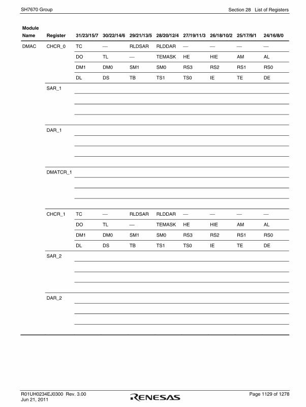
Section 28 List of Registers
R01UH0234EJ0300 Rev. 3.00 Page 1129 of 1278 Jun 21, 2011
SH7670 Group
Module
Name Register 31/23/15/7 30/22/14/6 29/21/13/5 28/20/12/4 27/19/11/3 26/18/10/2 25/17/9/1 24/16/8/0
DMAC CHCR_0 TC ⎯ RLDSAR RLDDAR ⎯ ⎯ ⎯ ⎯
DO TL ⎯ TEMASK HE HIE AM AL
DM1 DM0 SM1 SM0 RS3 RS2 RS1 RS0
DL DS TB TS1 TS0 IE TE DE
SAR_1
DAR_1
DMATCR_1
CHCR_1 TC ⎯ RLDSAR RLDDAR ⎯ ⎯ ⎯ ⎯
DO TL ⎯ TEMASK HE HIE AM AL
DM1 DM0 SM1 SM0 RS3 RS2 RS1 RS0
DL DS TB TS1 TS0 IE TE DE
SAR_2
DAR_2

Section 28 List of Registers
Page 1130 of 1278 R01UH0234EJ0300 Rev. 3.00 Jun 21, 2011
SH7670 Group
Module
Name Register 31/23/15/7 30/22/14/6 29/21/13/5 28/20/12/4 27/19/11/3 26/18/10/2 25/17/9/1 24/16/8/0
DMAC
DMATCR_2
CHCR_2 TC ⎯ RLDSAR RLDDAR ⎯ ⎯ ⎯ ⎯
⎯ ⎯ ⎯ TEMASK HE HIE ⎯ ⎯
DM1 DM0 SM1 SM0 RS3 RS2 RS1 RS0
⎯ ⎯ TB TS1 TS0 IE TE DE
SAR_3
DAR_3
DMATCR_3
CHCR_3 TC ⎯ RLDSAR RLDDAR ⎯ ⎯ ⎯ ⎯
⎯ ⎯ ⎯ TEMASK HE HIE ⎯ ⎯
DM1 DM0 SM1 SM0 RS3 RS2 RS1 RS0
⎯ ⎯ TB TS1 TS0 IE TE DE
SAR_4
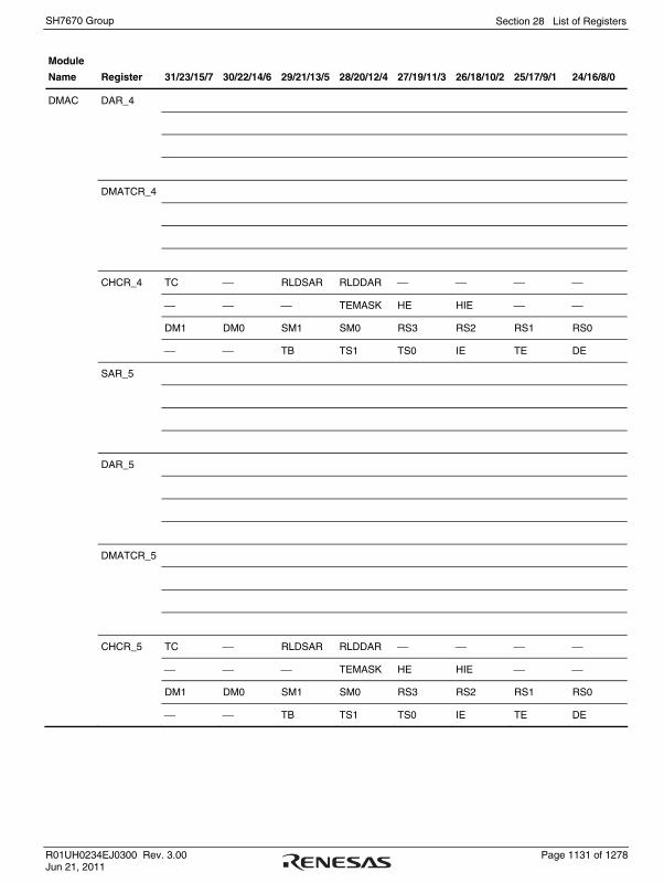
Section 28 List of Registers
R01UH0234EJ0300 Rev. 3.00 Page 1131 of 1278 Jun 21, 2011
SH7670 Group
Module
Name Register 31/23/15/7 30/22/14/6 29/21/13/5 28/20/12/4 27/19/11/3 26/18/10/2 25/17/9/1 24/16/8/0
DMAC DAR_4
DMATCR_4
CHCR_4 TC ⎯ RLDSAR RLDDAR ⎯ ⎯ ⎯ ⎯
⎯ ⎯ ⎯ TEMASK HE HIE ⎯ ⎯
DM1 DM0 SM1 SM0 RS3 RS2 RS1 RS0
⎯ ⎯ TB TS1 TS0 IE TE DE
SAR_5
DAR_5
DMATCR_5
CHCR_5 TC ⎯ RLDSAR RLDDAR ⎯ ⎯ ⎯ ⎯
⎯ ⎯ ⎯ TEMASK HE HIE ⎯ ⎯
DM1 DM0 SM1 SM0 RS3 RS2 RS1 RS0
⎯ ⎯ TB TS1 TS0 IE TE DE

Section 28 List of Registers
Page 1132 of 1278 R01UH0234EJ0300 Rev. 3.00 Jun 21, 2011
SH7670 Group
Module
Name Register 31/23/15/7 30/22/14/6 29/21/13/5 28/20/12/4 27/19/11/3 26/18/10/2 25/17/9/1 24/16/8/0
DMAC SAR_6
DAR_6
DMATCR_6
CHCR_6 TC ⎯ RLDSAR RLDDAR ⎯ ⎯ ⎯ ⎯
⎯ ⎯ ⎯ TEMASK HE HIE ⎯ ⎯
DM1 DM0 SM1 SM0 RS3 RS2 RS1 RS0
⎯ ⎯ TB TS1 TS0 IE TE DE
SAR_7
DAR_7
DMATCR_7

Section 28 List of Registers
R01UH0234EJ0300 Rev. 3.00 Page 1133 of 1278 Jun 21, 2011
SH7670 Group
Module
Name Register 31/23/15/7 30/22/14/6 29/21/13/5 28/20/12/4 27/19/11/3 26/18/10/2 25/17/9/1 24/16/8/0
DMAC CHCR_7 TC ⎯ RLDSAR RLDDAR ⎯ ⎯ ⎯ ⎯
⎯ ⎯ ⎯ TEMASK HE HIE ⎯ ⎯
DM1 DM0 SM1 SM0 RS3 RS2 RS1 RS0
⎯ ⎯ TB TS1 TS0 IE TE DE
RSAR_0
RDAR_0
RDMATCR_0
RSAR_1
RDAR_1
RDMATCR_1

Section 28 List of Registers
Page 1134 of 1278 R01UH0234EJ0300 Rev. 3.00 Jun 21, 2011
SH7670 Group
Module
Name Register 31/23/15/7 30/22/14/6 29/21/13/5 28/20/12/4 27/19/11/3 26/18/10/2 25/17/9/1 24/16/8/0
DMAC RSAR_2
RDAR_2
RDMATCR_2
RSAR_3
RDAR_3
RDMATCR_3
RSAR_4

Section 28 List of Registers
R01UH0234EJ0300 Rev. 3.00 Page 1135 of 1278 Jun 21, 2011
SH7670 Group
Module
Name Register 31/23/15/7 30/22/14/6 29/21/13/5 28/20/12/4 27/19/11/3 26/18/10/2 25/17/9/1 24/16/8/0
DMAC RDAR_4
RDMATCR_4
RSAR_5
RDAR_5
RDMATCR_5
RSAR_6
RDAR_6
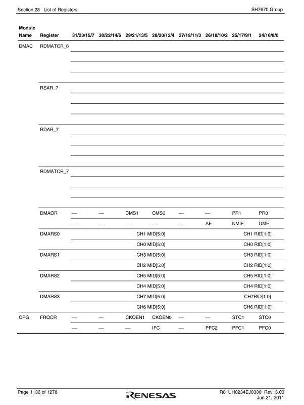
Section 28 List of Registers
Page 1136 of 1278 R01UH0234EJ0300 Rev. 3.00 Jun 21, 2011
SH7670 Group
Module
Name Register 31/23/15/7 30/22/14/6 29/21/13/5 28/20/12/4 27/19/11/3 26/18/10/2 25/17/9/1 24/16/8/0
DMAC
RDMATCR_6
RSAR_7
RDAR_7
RDMATCR_7
DMAOR ⎯ ⎯ CMS1 CMS0 ⎯ ⎯ PR1 PR0
⎯ ⎯ ⎯ ⎯ ⎯ AE NMIF DME
DMARS0 CH1 MID[5:0] CH1 RID[1:0]
CH0 MID[5:0] CH0 RID[1:0]
DMARS1 CH3 MID[5:0] CH3 RID[1:0]
CH2 MID[5:0] CH2 RID[1:0]
DMARS2 CH5 MID[5:0] CH5 RID[1:0]
CH4 MID[5:0] CH4 RID[1:0]
DMARS3 CH7 MID[5:0] CH7RID[1:0]
CH6 MID[5:0] CH6 RID[1:0]
CPG FRQCR ⎯ ⎯ CKOEN1 CKOEN0 ⎯ ⎯ STC1 STC0
⎯ ⎯ ⎯ IFC ⎯ PFC2 PFC1 PFC0
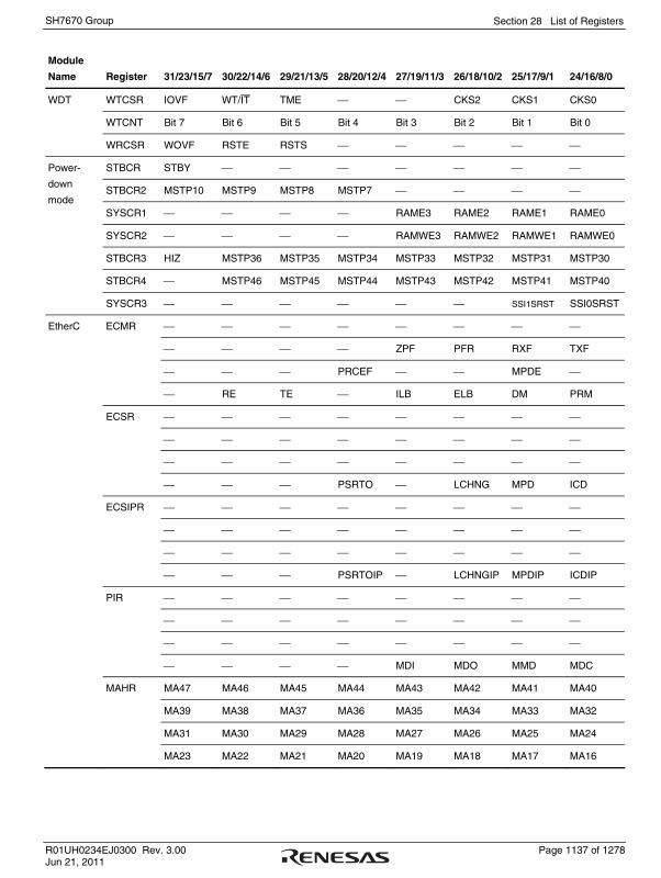
Section 28 List of Registers
R01UH0234EJ0300 Rev. 3.00 Page 1137 of 1278 Jun 21, 2011
SH7670 Group
Module
Name Register 31/23/15/7 30/22/14/6 29/21/13/5 28/20/12/4 27/19/11/3 26/18/10/2 25/17/9/1 24/16/8/0
WDT WTCSR IOVF WT/IT TME ⎯ ⎯ CKS2 CKS1 CKS0
WTCNT Bit 7 Bit 6 Bit 5 Bit 4 Bit 3 Bit 2 Bit 1 Bit 0
WRCSR WOVF RSTE RSTS ⎯ ⎯ ⎯ ⎯ ⎯
STBCR STBY ⎯ ⎯ ⎯ ⎯ ⎯ ⎯ ⎯
STBCR2 MSTP10 MSTP9 MSTP8 MSTP7 ⎯ ⎯ ⎯ ⎯
Power-
down
mode SYSCR1 ⎯ ⎯ ⎯ ⎯ RAME3 RAME2 RAME1 RAME0
SYSCR2 ⎯ ⎯ ⎯ ⎯ RAMWE3 RAMWE2 RAMWE1 RAMWE0
STBCR3 HIZ MSTP36 MSTP35 MSTP34 MSTP33 MSTP32 MSTP31 MSTP30
STBCR4 ⎯ MSTP46 MSTP45 MSTP44 MSTP43 MSTP42 MSTP41 MSTP40
SYSCR3 ⎯ ⎯ ⎯ ⎯ ⎯ ⎯ SSI1SRST SSI0SRST
EtherC ECMR ⎯ ⎯ ⎯ ⎯ ⎯ ⎯ ⎯ ⎯
⎯ ⎯ ⎯ ⎯ ZPF PFR RXF TXF
⎯ ⎯ ⎯ PRCEF ⎯ ⎯ MPDE ⎯
⎯ RE TE ⎯ ILB ELB DM PRM
ECSR ⎯ ⎯ ⎯ ⎯ ⎯ ⎯ ⎯ ⎯
⎯ ⎯ ⎯ ⎯ ⎯ ⎯ ⎯ ⎯
⎯ ⎯ ⎯ ⎯ ⎯ ⎯ ⎯ ⎯
⎯ ⎯ ⎯ PSRTO ⎯ LCHNG MPD ICD
ECSIPR ⎯ ⎯ ⎯ ⎯ ⎯ ⎯ ⎯ ⎯
⎯ ⎯ ⎯ ⎯ ⎯ ⎯ ⎯ ⎯
⎯ ⎯ ⎯ ⎯ ⎯ ⎯ ⎯ ⎯
⎯ ⎯ ⎯ PSRTOIP ⎯ LCHNGIP MPDIP ICDIP
PIR ⎯ ⎯ ⎯ ⎯ ⎯ ⎯ ⎯ ⎯
⎯ ⎯ ⎯ ⎯ ⎯ ⎯ ⎯ ⎯
⎯ ⎯ ⎯ ⎯ ⎯ ⎯ ⎯ ⎯
⎯ ⎯ ⎯ ⎯ MDI MDO MMD MDC
MAHR MA47 MA46 MA45 MA44 MA43 MA42 MA41 MA40
MA39 MA38 MA37 MA36 MA35 MA34 MA33 MA32
MA31 MA30 MA29 MA28 MA27 MA26 MA25 MA24
MA23 MA22 MA21 MA20 MA19 MA18 MA17 MA16

Section 28 List of Registers
Page 1138 of 1278 R01UH0234EJ0300 Rev. 3.00 Jun 21, 2011
SH7670 Group
Module
Name Register 31/23/15/7 30/22/14/6 29/21/13/5 28/20/12/4 27/19/11/3 26/18/10/2 25/17/9/1 24/16/8/0
EtherC MALR ⎯ ⎯ ⎯ ⎯ ⎯ ⎯ ⎯ ⎯
⎯ ⎯ ⎯ ⎯ ⎯ ⎯ ⎯ ⎯
MA15 MA14 MA13 MA12 MA11 MA10 MA9 MA8
MA7 MA6 MA5 MA4 MA3 MA2 MA1 MA0
RFLR ⎯ ⎯ ⎯ ⎯ ⎯ ⎯ ⎯ ⎯
⎯ ⎯ ⎯ ⎯ ⎯ ⎯ ⎯ ⎯
⎯ ⎯ ⎯ ⎯ RFL11 RFL10 RFL9 RFL8
RFL7 RFL6 RFL5 RFL4 RFL3 RFL2 RFL1 RFL0
PSR ⎯ ⎯ ⎯ ⎯ ⎯ ⎯ ⎯ ⎯
⎯ ⎯ ⎯ ⎯ ⎯ ⎯ ⎯ ⎯
⎯ ⎯ ⎯ ⎯ ⎯ ⎯ ⎯ ⎯
⎯ ⎯ ⎯ ⎯ ⎯ ⎯ ⎯ LMON
TROCR TROC31 TROC30 TROC29 TROC28 TROC27 TROC26 TROC25 TROC24
TROC23 TROC22 TROC21 TROC20 TROC19 TROC18 TROC17 TROC16
TROC15 TROC14 TROC13 TROC12 TROC11 TROC10 TROC9 TROC8
TROC7 TROC6 TROC5 TROC4 TROC3 TROC2 TROC1 TROC0
CDCR COSDC31 COSDC30 COSDC29 COSDC28 COSDC27 COSDC26 COSDC25 COSDC24
COSDC23 COSDC22 COSDC21 COSDC20 COSDC19 COSDC18 COSDC17 COSDC16
COSDC15 COSDC14 COSDC13 COSDC12 COSDC11 COSDC10 COSDC9 COSDC8
COSDC7 COSDC6 COSDC5 COSDC4 COSDC3 COSDC2 COSDC1 COSDC0
LCCR LCC31 LCC30 LCC29 LCC28 LCC27 LCC26 LCC25 LCC24
LCC23 LCC22 LCC21 LCC20 LCC19 LCC18 LCC17 LCC16
LCC15 LCC14 LCC13 LCC12 LCC11 LCC10 LCC9 LCC8
LCC7 LCC6 LCC5 LCC4 LCC3 LCC2 LCC1 LCC0
CNDCR CNDC31 CNDC30 CNDC29 CNDC28 CNDC27 CNDC26 CNDC25 CNDC24
CNDC23 CNDC22 CNDC21 CNDC20 CNDC19 CNDC18 CNDC17 CNDC16
CNDC15 CNDC14 CNDC13 CNDC12 CNDC11 CNDC10 CNDC9 CNDC8
CNDC7 CNDC6 CNDC5 CNDC4 CNDC3 CNDC2 CNDC1 CNDC0

Section 28 List of Registers
R01UH0234EJ0300 Rev. 3.00 Page 1139 of 1278 Jun 21, 2011
SH7670 Group
Module
Name Register 31/23/15/7 30/22/14/6 29/21/13/5 28/20/12/4 27/19/11/3 26/18/10/2 25/17/9/1 24/16/8/0
EtherC CEFCR CEFC31 CEFC30 CEFC29 CEFC28 CEFC27 CEFC26 CEFC25 CEFC24
CEFC23 CEFC22 CEFC21 CEFC20 CEFC19 CEFC18 CEFC17 CEFC16
CEFC15 CEFC14 CEFC13 CEFC12 CEFC11 CEFC10 CEFC9 CEFC8
CEFC7 CEFC6 CEFC5 CEFC4 CEFC3 CEFC2 CEFC1 CEFC0
FRECR FREC31 FREC30 FREC29 FREC28 FREC27 FREC26 FREC25 FREC24
FREC23 FREC22 FREC21 FREC20 FREC19 FREC18 FREC17 FREC16
FREC15 FREC14 FREC13 FREC12 FREC11 FREC10 FREC9 FREC8
FREC7 FREC6 FREC5 FREC4 FREC3 FREC2 FREC1 FREC0
TSFRCR TSFC31 TSFC30 TSFC29 TSFC28 TSFC27 TSFC26 TSFC25 TSFC24
TSFC23 TSFC22 TSFC21 TSFC20 TSFC19 TSFC18 TSFC17 TSFC16
TSFC15 TSFC14 TSFC13 TSFC12 TSFC11 TSFC10 TSFC9 TSFC8
TSFC7 TSFC6 TSFC5 TSFC4 TSFC3 TSFC2 TSFC1 TSFC0
TLFRCR TLFC31 TLFC30 TLFC29 TLFC28 TLFC27 TLFC26 TLFC25 TLFC24
TLFC23 TLFC22 TLFC21 TLFC20 TLFC19 TLFC18 TLFC17 TLFC16
TLFC15 TLFC14 TLFC13 TLFC12 TLFC11 TLFC10 TLFC9 TLFC8
TLFC7 TLFC6 TLFC5 TLFC4 TLFC3 TLFC2 TLFC1 TLFC0
RFCR RFC31 RFC30 RFC29 RFC28 RFC27 RFC26 RFC25 RFC24
RFC23 RFC22 RFC21 RFC20 RFC19 RFC18 RFC17 RFC16
RFC15 RFC14 RFC13 RFC12 RFC11 RFC10 RFC9 RFC8
RFC7 RFC6 RFC5 RFC4 RFC3 RFC2 RFC1 RFC0
MAFCR MAFC31 MAFC30 MAFC29 MAFC28 MAFC27 MAFC26 MAFC25 MAFC24
MAFC23 MAFC22 MAFC21 MAFC20 MAFC19 MAFC18 MAFC17 MAFC16
MAFC15 MAFC14 MAFC13 MAFC12 MAFC11 MAFC10 MAFC9 MAFC8
MAFC7 MAFC6 MAFC5 MAFC4 MAFC3 MAFC2 MAFC1 MAFC0
IPGR ⎯ ⎯ ⎯ ⎯ ⎯ ⎯ ⎯ ⎯
⎯ ⎯ ⎯ ⎯ ⎯ ⎯ ⎯ ⎯
⎯ ⎯ ⎯ ⎯ ⎯ ⎯ ⎯ ⎯
⎯ ⎯ ⎯ IPG4 IPG3 IPG2 IPG1 IPG0
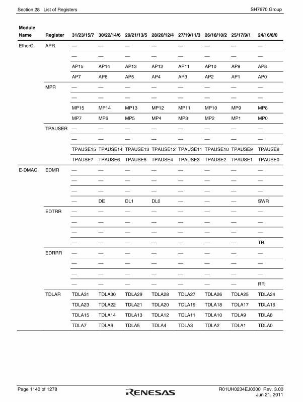
Section 28 List of Registers
Page 1140 of 1278 R01UH0234EJ0300 Rev. 3.00 Jun 21, 2011
SH7670 Group
Module
Name Register 31/23/15/7 30/22/14/6 29/21/13/5 28/20/12/4 27/19/11/3 26/18/10/2 25/17/9/1 24/16/8/0
EtherC APR ⎯ ⎯ ⎯ ⎯ ⎯ ⎯ ⎯ ⎯
⎯ ⎯ ⎯ ⎯ ⎯ ⎯ ⎯ ⎯
AP15 AP14 AP13 AP12 AP11 AP10 AP9 AP8
AP7 AP6 AP5 AP4 AP3 AP2 AP1 AP0
MPR ⎯ ⎯ ⎯ ⎯ ⎯ ⎯ ⎯ ⎯
⎯ ⎯ ⎯ ⎯ ⎯ ⎯ ⎯ ⎯
MP15 MP14 MP13 MP12 MP11 MP10 MP9 MP8
MP7 MP6 MP5 MP4 MP3 MP2 MP1 MP0
TPAUSER ⎯ ⎯ ⎯ ⎯ ⎯ ⎯ ⎯ ⎯
⎯ ⎯ ⎯ ⎯ ⎯ ⎯ ⎯ ⎯
TPAUSE15 TPAUSE14 TPAUSE13 TPAUSE12 TPAUSE11 TPAUSE10 TPAUSE9 TPAUSE8
TPAUSE7 TPAUSE6 TPAUSE5 TPAUSE4 TPAUSE3 TPAUSE2 TPAUSE1 TPAUSE0
E-DMAC EDMR ⎯ ⎯ ⎯ ⎯ ⎯ ⎯ ⎯ ⎯
⎯ ⎯ ⎯ ⎯ ⎯ ⎯ ⎯ ⎯
⎯ ⎯ ⎯ ⎯ ⎯ ⎯ ⎯ ⎯
⎯ DE DL1 DL0 ⎯ ⎯ ⎯ SWR
EDTRR ⎯ ⎯ ⎯ ⎯ ⎯ ⎯ ⎯ ⎯
⎯ ⎯ ⎯ ⎯ ⎯ ⎯ ⎯ ⎯
⎯ ⎯ ⎯ ⎯ ⎯ ⎯ ⎯ ⎯
⎯ ⎯ ⎯ ⎯ ⎯ ⎯ ⎯ TR
EDRRR ⎯ ⎯ ⎯ ⎯ ⎯ ⎯ ⎯ ⎯
⎯ ⎯ ⎯ ⎯ ⎯ ⎯ ⎯ ⎯
⎯ ⎯ ⎯ ⎯ ⎯ ⎯ ⎯ ⎯
⎯ ⎯ ⎯ ⎯ ⎯ ⎯ ⎯ RR
TDLAR TDLA31 TDLA30 TDLA29 TDLA28 TDLA27 TDLA26 TDLA25 TDLA24
TDLA23 TDLA22 TDLA21 TDLA20 TDLA19 TDLA18 TDLA17 TDLA16
TDLA15 TDLA14 TDLA13 TDLA12 TDLA11 TDLA10 TDLA9 TDLA8
TDLA7 TDLA6 TDLA5 TDLA4 TDLA3 TDLA2 TDLA1 TDLA0

Section 28 List of Registers
R01UH0234EJ0300 Rev. 3.00 Page 1141 of 1278 Jun 21, 2011
SH7670 Group
Module
Name Register 31/23/15/7 30/22/14/6 29/21/13/5 28/20/12/4 27/19/11/3 26/18/10/2 25/17/9/1 24/16/8/0
E-DMAC RDLAR RDLA31 RDLA30 RDLA29 RDLA28 RDLA27 RDLA26 RDLA25 RDLA24
RDLA23 RDLA22 RDLA21 RDLA20 RDLA19 RDLA18 RDLA17 RDLA16
RDLA15 RDLA14 RDLA13 RDLA12 RDLA11 RDLA10 RDLA9 RDLA8
RDLA7 RDLA6 RDLA5 RDLA4 RDLA3 RDLA2 RDLA1 RDLA0
EESR ⎯ TWB ⎯ ⎯ ⎯ TABT RABT RFCOF
ADE ECI TC TDE TFUF FR RDE RFOF
⎯ ⎯ ⎯ ⎯ CND DLC CD TRO
RMAF ⎯ ⎯ RRF RTLF RTSF PRE CERF
EESIPR ⎯ TWBIP ⎯ ⎯ ⎯ TABTIP RABTIP RFCOFIP
ADEIP ECIIP TCIP TDEIP TFUFIP FRIP RDEIP RFOFIP
⎯ ⎯ ⎯ ⎯ CNDIP DLCIP CDIP TROIP
RMAFIP ⎯ ⎯ RRFIP RTLFIP RTSFIP PREIP CERFIP
TRSCER ⎯ ⎯ ⎯ ⎯ ⎯ ⎯ ⎯ ⎯
⎯ ⎯ ⎯ ⎯ ⎯ ⎯ ⎯ ⎯
⎯ ⎯ ⎯ ⎯ CNDCE DLCCE CDCE TROCE
RMAFCE ⎯ ⎯ RRFCE RTLFCE RTSFCE PRECE CERFCE
RMFCR ⎯ ⎯ ⎯ ⎯ ⎯ ⎯ ⎯ ⎯
⎯ ⎯ ⎯ ⎯ ⎯ ⎯ ⎯ ⎯
MFC15 MFC14 MFC13 MFC12 MFC11 MFC10 MFC9 MFC8
MFC7 MFC6 MFC5 MFC4 MFC3 MFC2 MFC1 MFC0
TFTR ⎯ ⎯ ⎯ ⎯ ⎯ ⎯ ⎯ ⎯
⎯ ⎯ ⎯ ⎯ ⎯ ⎯ ⎯ ⎯
⎯ ⎯ ⎯ ⎯ ⎯ TFT10 TFT9 TFT8
TFT7 TFT6 TFT5 TFT4 TFT3 TFT2 TFT1 TFT0
FDR ⎯ ⎯ ⎯ ⎯ ⎯ ⎯ ⎯ ⎯
⎯ ⎯ ⎯ ⎯ ⎯ ⎯ ⎯ ⎯
⎯ ⎯ ⎯ ⎯ ⎯ TFD2 TFD1 TFD0
⎯ ⎯ ⎯ ⎯ ⎯ RFD2 RFD1 RFD0

Section 28 List of Registers
Page 1142 of 1278 R01UH0234EJ0300 Rev. 3.00 Jun 21, 2011
SH7670 Group
Module
Name Register 31/23/15/7 30/22/14/6 29/21/13/5 28/20/12/4 27/19/11/3 26/18/10/2 25/17/9/1 24/16/8/0
E-DMAC RMCR ⎯ ⎯ ⎯ ⎯ ⎯ ⎯ ⎯ ⎯
⎯ ⎯ ⎯ ⎯ ⎯ ⎯ ⎯ ⎯
⎯ ⎯ ⎯ ⎯ ⎯ ⎯ ⎯ ⎯
⎯ ⎯ ⎯ ⎯ ⎯ ⎯ ⎯ RNC
EDOCR ⎯ ⎯ ⎯ ⎯ ⎯ ⎯ ⎯ ⎯
⎯ ⎯ ⎯ ⎯ ⎯ ⎯ ⎯ ⎯
⎯ ⎯ ⎯ ⎯ ⎯ ⎯ ⎯ ⎯
⎯ ⎯ ⎯ ⎯ FEC AEC EDH ⎯
FCFTR ⎯ ⎯ ⎯ ⎯ ⎯ ⎯ ⎯ ⎯
⎯ ⎯ ⎯ ⎯ ⎯ RFF2 RFF1 RFF0
⎯ ⎯ ⎯ ⎯ ⎯ ⎯ ⎯ ⎯
⎯ ⎯ ⎯ ⎯ ⎯ RFD2 RFD1 RFD0
RPADIR ⎯ ⎯ ⎯ ⎯ ⎯ ⎯ ⎯ ⎯
⎯ ⎯ ⎯ ⎯ ⎯ ⎯ PADS1 PADS0
⎯ ⎯ ⎯ ⎯ ⎯ ⎯ ⎯ ⎯
⎯ ⎯ PADR5 PADR4 PADR3 PADR2 PADR1 PADR0
TRIMD ⎯ ⎯ ⎯ ⎯ ⎯ ⎯ ⎯ ⎯
⎯ ⎯ ⎯ ⎯ ⎯ ⎯ ⎯ ⎯
⎯ ⎯ ⎯ ⎯ ⎯ ⎯ ⎯ ⎯
⎯ ⎯ ⎯ ⎯ ⎯ ⎯ ⎯ TIS
RBWAR RBWA31 RBWA30 RBWA29 RBWA28 RBWA27 RBWA26 RBWA25 RBWA24
RBWA23 RBWA22 RBWA21 RBWA20 RBWA19 RBWA18 RBWA17 RBWA16
RBWA15 RBWA14 RBWA13 RBWA12 RBWA11 RBWA10 RBWA9 RBWA8
RBWA7 RBWA6 RBWA5 RBWA4 RBWA3 RBWA2 RBWA1 RBWA0
RDFAR RDFA31 RDFA30 RDFA29 RDFA28 RDFA27 RDFA26 RDFA25 RDFA24
RDFA23 RDFA22 RDFA21 RDFA20 RDFA19 RDFA18 RDFA17 RDFA16
RDFA15 RDFA14 RDFA13 RDFA12 RDFA11 RDFA10 RDFA9 RDFA8
RDFA7 RDFA6 RDFA5 RDFA4 RDFA3 RDFA2 RDFA1 RDFA0

Section 28 List of Registers
R01UH0234EJ0300 Rev. 3.00 Page 1143 of 1278 Jun 21, 2011
SH7670 Group
Module
Name Register 31/23/15/7 30/22/14/6 29/21/13/5 28/20/12/4 27/19/11/3 26/18/10/2 25/17/9/1 24/16/8/0
E-DMAC TBRAR TBRA31 TBRA30 TBRA29 TBRA28 TBRA27 TBRA26 TBRA25 TBRA24
TBRA23 TBRA22 TBRA21 TBRA20 TBRA19 TBRA18 TBRA17 TBRA16
TBRA15 TBRA14 TBRA13 TBRA12 TBRA11 TBRA10 TBRA9 TBRA8
TBRA7 TBRA6 TBRA5 TBRA4 TBRA3 TBRA2 TBRA1 TBRA0
TDFAR TDFA31 TDFA30 TDFA29 TDFA28 TDFA27 TDFA26 TDFA25 TDFA24
TDFA23 TDFA22 TDFA21 TDFA20 TDFA19 TDFA18 TDFA17 TDFA16
TDFA15 TDFA14 TDFA13 TDFA12 TDFA11 TDFA10 TDFA9 TDFA8
TDFA7 TDFA6 TDFA5 TDFA4 TDFA3 TDFA2 TDFA1 TDFA0
CSMR CSEBL CSMD ⎯ ⎯ ⎯ ⎯ ⎯ ⎯
⎯ ⎯ ⎯ ⎯ ⎯ ⎯ ⎯ ⎯
⎯ ⎯ ⎯ ⎯ ⎯ ⎯ ⎯ ⎯
⎯ ⎯ SB5 SB4 SB3 SB2 SB1 SB0
CSSBM ⎯ ⎯ ⎯ ⎯ ⎯ ⎯ ⎯ ⎯
⎯ ⎯ ⎯ ⎯ ⎯ ⎯ ⎯ ⎯
⎯ ⎯ ⎯ ⎯ ⎯ ⎯ ⎯ ⎯
⎯ ⎯ SBM5 SBM4 SBM3 SBM2 SBM1 SBM0
CSSMR ⎯ ⎯ ⎯ ⎯ ⎯ ⎯ ⎯ ⎯
⎯ ⎯ ⎯ ⎯ ⎯ ⎯ ⎯ ⎯
CS15 CS14 CS13 CS12 CS11 CS10 CS9 CS8
CS7 CS6 CS5 CS4 CS3 CS2 CS1 CS0
A-DMAC C0C ⎯ ⎯ ⎯ ⎯ ⎯ ⎯ ⎯ ⎯
⎯ ⎯ ⎯ ⎯ ⎯ ⎯ ⎯ C0C_R
⎯ ⎯ ⎯ C0C_DWF ⎯ ⎯ ⎯ C0C_VLD
⎯ ⎯ ⎯ C0C_EIE ⎯ ⎯ ⎯ C0C_E
C0M ⎯ ⎯ ⎯ ⎯ ⎯ ⎯ ⎯ ⎯
⎯ ⎯ ⎯ ⎯ ⎯ ⎯ ⎯ ⎯
⎯ ⎯ ⎯ ⎯ ⎯ ⎯ ⎯ ⎯
⎯ ⎯ ⎯ C0M_LIE ⎯ ⎯ ⎯ ⎯

Section 28 List of Registers
Page 1144 of 1278 R01UH0234EJ0300 Rev. 3.00 Jun 21, 2011
SH7670 Group
Module
Name Register 31/23/15/7 30/22/14/6 29/21/13/5 28/20/12/4 27/19/11/3 26/18/10/2 25/17/9/1 24/16/8/0
A-DMAC C0I ⎯ ⎯ ⎯ ⎯ ⎯ ⎯ ⎯ ⎯
⎯ ⎯ ⎯ ⎯ ⎯ ⎯ ⎯ ⎯
⎯ ⎯ ⎯ C0I_DI ⎯ ⎯ ⎯ C0I_LI
⎯ ⎯ ⎯ ⎯ ⎯ ⎯ ⎯ C0I_EI
C0DSA C0DSA[31:24]
C0DSA[23:16]
C0DSA[15:8]
C0DSA[7:0]
C0DCA C0DCA[31:24]
C0DCA[23:16]
C0DCA[15:8]
C0DCA[7:0]
C0D0 C0CRDO[3:0] C0CHDO[3:0]
C0SO[3:0] C0DA C0SA C0CSM[1:0]
⎯ ⎯ ⎯ ⎯ ⎯ ⎯ ⎯ ⎯
⎯ ⎯ ⎯ ⎯ ⎯ C0F[2:0]
C0D1 C0D1[31:24]
C0D1[23:16]
C0D1[15:8]
C0D1[7:0]
C0D2 C0D2[31:24]
C0D2[23:16]
C0D2[15:8]
C0D2[7:0]
C0D3 ⎯ ⎯ C0DWE C0DIE ⎯ ⎯ ⎯ ⎯
⎯ ⎯ ⎯ ⎯ ⎯ ⎯ ⎯ ⎯
C0D3[15:8]
C0D3[7:0]

Section 28 List of Registers
R01UH0234EJ0300 Rev. 3.00 Page 1145 of 1278 Jun 21, 2011
SH7670 Group
Module
Name Register 31/23/15/7 30/22/14/6 29/21/13/5 28/20/12/4 27/19/11/3 26/18/10/2 25/17/9/1 24/16/8/0
A-DMAC C0D4 C0D4[31:24]
C0D4[23:16]
C0D4[15:8]
C0D4[7:1] ⎯
C1C ⎯ ⎯ ⎯ ⎯ ⎯ ⎯ ⎯ ⎯
⎯ ⎯ ⎯ ⎯ ⎯ ⎯ ⎯ C1C_R
⎯ ⎯ ⎯ C1C_DWF ⎯ ⎯ ⎯ C1C_VLD
⎯ ⎯ ⎯ C1C_EIE ⎯ ⎯ ⎯ C1C_E
C1M ⎯ ⎯ ⎯ ⎯ ⎯ ⎯ ⎯ ⎯
⎯ ⎯ ⎯ ⎯ ⎯ ⎯ ⎯ ⎯
⎯ ⎯ ⎯ ⎯ ⎯ ⎯ ⎯ ⎯
⎯ ⎯ ⎯ C1M_LIE ⎯ ⎯ ⎯ ⎯
C1I ⎯ ⎯ ⎯ ⎯ ⎯ ⎯ ⎯ ⎯
⎯ ⎯ ⎯ ⎯ ⎯ ⎯ ⎯ ⎯
⎯ ⎯ ⎯ C1I_DI ⎯ ⎯ ⎯ C1I_LI
⎯ ⎯ ⎯ ⎯ ⎯ ⎯ ⎯ C1I_EI
C1DSA C1DSA[31:24]
C1DSA[23:16]
C1DSA[15:8]
C1DSA[7:0]
C1DCA C1DCA[31:24]
C1DCA[23:16]
C1DCA[15:8]
C1DCA[7:0]
C1D0 C1CRDO[3:0] C1CHDO[3:0]
C1SO[3:0] C1DA C1SA C1CSM[1:0]
⎯ ⎯ ⎯ ⎯ ⎯ ⎯ ⎯ ⎯
⎯ ⎯ ⎯ ⎯ ⎯ C1F[2:0]

Section 28 List of Registers
Page 1146 of 1278 R01UH0234EJ0300 Rev. 3.00 Jun 21, 2011
SH7670 Group
Module
Name Register 31/23/15/7 30/22/14/6 29/21/13/5 28/20/12/4 27/19/11/3 26/18/10/2 25/17/9/1 24/16/8/0
A-DMAC C1D1 C1D1[31:24]
C1D1[23:16]
C1D1[15:8]
C1D1[7:0]
C1D2 C1D2[31:24]
C1D2[23:16]
C1D2[15:8]
C1D2[7:0]
C1D3 ⎯ ⎯ C1DWE C1DIE ⎯ ⎯ ⎯ ⎯
⎯ ⎯ ⎯ ⎯ ⎯ ⎯ ⎯ ⎯
C1D3[15:8]
C1D3[7:0]
C1D4 C1D4[31:24]
C1D4[23:16]
C1D4[15:8]
C1D4[7:0]
FECC ⎯ ⎯ ⎯ FECC_R ⎯ ⎯ ⎯ FECC_DWF
⎯ ⎯ ⎯ FECC_DWE ⎯ ⎯ ⎯ FECC_DIE
⎯ ⎯ ⎯ FECC_LIE ⎯ ⎯ ⎯ FECC_NIE
⎯ ⎯ ⎯ FECC_EIE ⎯ ⎯ ⎯ FECC_E
FECI ⎯ ⎯ ⎯ ⎯ ⎯ ⎯ ⎯ ⎯
⎯ ⎯ ⎯ ⎯ ⎯ ⎯ ⎯ ⎯
⎯ ⎯ ⎯ FECI_DI ⎯ ⎯ ⎯ FECI_LI
⎯ ⎯ ⎯ FECI_NI ⎯ ⎯ ⎯ FECI_EI
FECDSA FECDSA[31:24]
FECDSA[23:16]
FECDSA[15:8]
FECDSA[7:0]

Section 28 List of Registers
R01UH0234EJ0300 Rev. 3.00 Page 1147 of 1278 Jun 21, 2011
SH7670 Group
Module
Name Register 31/23/15/7 30/22/14/6 29/21/13/5 28/20/12/4 27/19/11/3 26/18/10/2 25/17/9/1 24/16/8/0
A-DMAC FECDCA FECDCA[31:24]
FECDCA[23:16]
FECDCA[15:8]
FECDCA[7:0]
FECD00 FECD00_SZ[15:8]
FECD00_SZ[7:0]
FECD00_DO[3:0] FECD00_SO[3:0]
FECD00_SN[3:0] FECD00_
DRE
FECD00_F[2:0]
FECD01D0A FECD01D0A[31:24]
FECD01D0A[23:16]
FECD01D0A[15:8]
FECD01D0A[7:0]
FECD02S0A FECD02S0A[31:24]
FECD02S0A[23:16]
FECD02S0A[15:8]
FECD02S0A[7:0]
FECD03S1A FECD03S1A[31:24]
FECD03S1A[23:16]
FECD03S1A[15:8]
FECD03S1A[7:0]
STIF0 STMDR_0 ⎯ ⎯ ⎯ ⎯ ⎯ ⎯ ⎯ ⎯
⎯ ⎯ ⎯ ⎯ ⎯ ⎯ ⎯ ⎯
⎯ LSBSEL EDGSEL CLKSEL CKFRSEL3 CKFRSEL2 CKFRSEL1 CKFRSEL0
REQACSEL VLDACTSEL SYCACTSEL IOSEL IFMDSEL3 IFMDSEL2 IFMDSEL1 IFMDSEL0
STCTLR_0 ⎯ ⎯ ⎯ ⎯ ⎯ ⎯ ⎯ ⎯
⎯ ⎯ ⎯ ⎯ ⎯ ⎯ ⎯ ⎯
⎯ ⎯ ⎯ ⎯ RCVTM2 RCVTM1 RCVTM0 RCV
TRICK ⎯ ⎯ ⎯ ⎯ REQEN EN SRST

Section 28 List of Registers
Page 1148 of 1278 R01UH0234EJ0300 Rev. 3.00 Jun 21, 2011
SH7670 Group
Module
Name Register 31/23/15/7 30/22/14/6 29/21/13/5 28/20/12/4 27/19/11/3 26/18/10/2 25/17/9/1 24/16/8/0
STIF0 ⎯ ⎯ ⎯ ⎯ ⎯ ⎯ ⎯ ⎯
STCNTCR_0
⎯ ⎯ ⎯ ⎯ ⎯ ⎯ ⎯ ⎯
⎯ ⎯ ⎯ ⎯ ⎯ ⎯ ⎯ ⎯
⎯ ⎯ ⎯ ⎯ CRD CSTP CSET CRST
VLU31 VLU30 VLU29 VLU28 VLU27 VLU26 VLU25 VLU24
STCNTVR_0
VLU23 VLU22 VLU21 VLU20 VLU19 VLU18 VLU17 VLU16
VLU15 VLU14 VLU13 VLU12 VLU11 VLU10 VLU9 VLU8
VLU7 VLU6 VLU5 VLU4 VLU3 VLU2 VLU1 VLU0
STSTR_0 ⎯ ⎯ ⎯ ⎯ ⎯ ⎯ ⎯ ⎯
⎯ ⎯ ⎯ ⎯ ⎯ ⎯ ⎯ ⎯
⎯ ⎯ ⎯ LKZF LKF DISF UNZF PCRF
TENDF RENDF RCVF3 RCVF2 RCVF1 UPF OPF OVF
STIER_0 ⎯ ⎯ ⎯ ⎯ ⎯ ⎯ ⎯ ⎯
⎯ ⎯ ⎯ ⎯ ⎯ ⎯ ⎯ ⎯
⎯ ⎯ ⎯ LKZE LKE DISE UNZE PCRE
TENDE RENDE RCVE3 RCVE2 RCVE1 UPE OPE OVE
SIZE[31:24]
STSIZER_0
SIZE[23:16]
SIZE[15:8]
SIZE[7:0]
⎯ ⎯ ⎯ PID12 PID11 PID10 PID9 PID8
STPWMMR_0
PID7 PID6 PID5 PID4 PID3 PID2 PID1 PID0
PIDEN PWMUEN PWMSEL PWMSEL2 PWMCYC[3:0]
PWMSFT[3:0] PWMDIV[3:0]
⎯ ⎯ ⎯ ⎯ ⎯ ⎯ ⎯ ⎯
STPWMCR_0
⎯ ⎯ ⎯ ⎯ ⎯ ⎯ ⎯ ⎯
⎯ ⎯ ⎯ ⎯ ⎯ ⎯ ⎯ STCXP
PWMBRS PWMBWP PWMRS PWMWP STCRS STCWP PCRRS PCRWP

Section 28 List of Registers
R01UH0234EJ0300 Rev. 3.00 Page 1149 of 1278 Jun 21, 2011
SH7670 Group
Module
Name Register 31/23/15/7 30/22/14/6 29/21/13/5 28/20/12/4 27/19/11/3 26/18/10/2 25/17/9/1 24/16/8/0
STIF0 PWMB15 PWMB14 PWMB13 PWMB12 PWMB11 PWMB10 PWMB9 PWMB8
STPWMR_0
PWMB7 PWMB6 PWMB5 PWMB4 PWMB3 PWMB2 PWMB1 PWMB0
PWM15 PWM14 PWM13 PWM12 PWM11 PWM10 PWM9 PWM8
PWM7 PWM6 PWM5 PWM4 PWM3 PWM2 PWM1 PWM0
⎯ ⎯ ⎯ ⎯ ⎯ ⎯ ⎯ ⎯
STPCR0R_0
⎯ ⎯ ⎯ ⎯ ⎯ ⎯ ⎯ ⎯
⎯ ⎯ ⎯ ⎯ ⎯ ⎯ PCRB32 PCRB31
PCRB30 PCRB29 PCRB28 PCRB27 PCRB26 PCRB25 PCRB24 PCRB23
PCRB22 PCRB21 PCRB20 PCRB19 PCRB18 PCRB17 PCRB16 PCRB15
STPCR1R_0
PCRB14 PCRB13 PCRB12 PCRB11 PCRB10 PCRB9 PCRB8 PCRB7
PCRB6 PCRB5 PCRB4 PCRB3 PCRB2 PCRB1 PCRB0 PCRX8
PCRX7 PCRX6 PCRX5 PCRX4 PCRX3 PCRX2 PCRX1 PCRX0
⎯ ⎯ ⎯ ⎯ ⎯ ⎯ ⎯ ⎯
STSTC0R_0
⎯ ⎯ ⎯ ⎯ ⎯ ⎯ ⎯ ⎯
⎯ ⎯ ⎯ ⎯ ⎯ ⎯ STCB32 STCB31
STCB30 STCB29 STCB28 STCB27 STCB26 STCB25 STCB24 STCB23
STCB22 STCB21 STCB20 STCB19 STCB18 STCB17 STCB16 STCB15
STSTC1R_0
STCB14 STCB13 STCB12 STCB11 STCB10 STCB9 STCB8 STCB7
STCB6 STCB5 STCB4 STCB3 STCB2 STCB1 STCB0 STCX8
STCX7 STCX6 STCX5 STCX4 STCX3 STCX2 STCX1 STCX0
STLKCR_0 ⎯ ⎯ ⎯ ⎯ ⎯ ⎯ LKWP ULWP
ULCNT3 ULCNT2 ULCNT1 ULCNT0 LKCNT3 LKCNT2 LKCNT1 LKCNT0
GAIN3 GAIN2 GAIN1 GAIN0 LKCYC3 LKCYC2 LKCYC1 LKCYC0
ULREF3 ULREF2 ULREF1 ULREF0 LKREF3 LKREF2 LKREF1 LKREF0
STMON31 STMON30 STMON29 STMON28 STMON27 STMON26 STMON25 STMON24
STDBGR_0
STMON23 STMON22 STMON21 STMON20 STMON19 STMON18 STMON17 STMON16
STMON15 STMON14 STMON13 STMON12 STMON11 STMON10 STMON9 STMON8
STMON7 STMON6 STMON5 STMON4 STMON3 STMON2 STMON1 STMON0
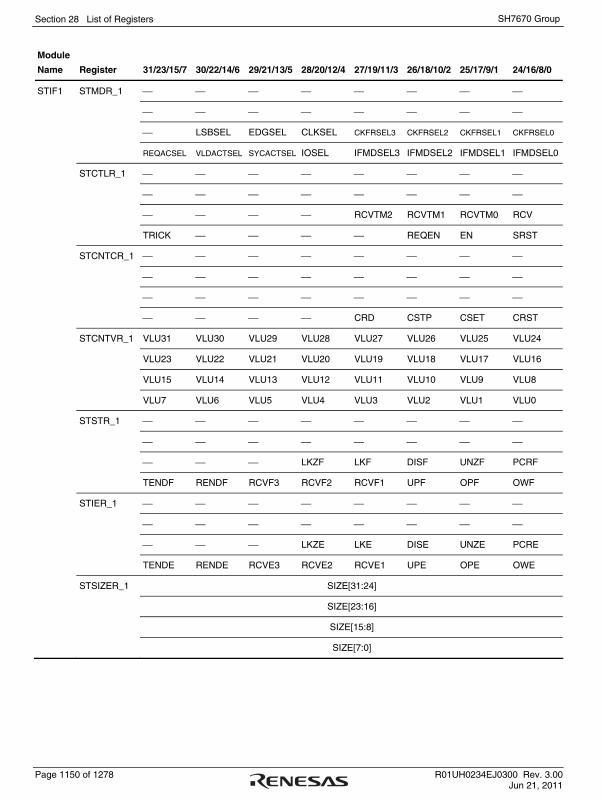
Section 28 List of Registers
Page 1150 of 1278 R01UH0234EJ0300 Rev. 3.00 Jun 21, 2011
SH7670 Group
Module
Name Register 31/23/15/7 30/22/14/6 29/21/13/5 28/20/12/4 27/19/11/3 26/18/10/2 25/17/9/1 24/16/8/0
STIF1 STMDR_1 ⎯ ⎯ ⎯ ⎯ ⎯ ⎯ ⎯ ⎯
⎯ ⎯ ⎯ ⎯ ⎯ ⎯ ⎯ ⎯
⎯ LSBSEL EDGSEL CLKSEL CKFRSEL3 CKFRSEL2 CKFRSEL1 CKFRSEL0
REQACSEL VLDACTSEL SYCACTSEL IOSEL IFMDSEL3 IFMDSEL2 IFMDSEL1 IFMDSEL0
STCTLR_1 ⎯ ⎯ ⎯ ⎯ ⎯ ⎯ ⎯ ⎯
⎯ ⎯ ⎯ ⎯ ⎯ ⎯ ⎯ ⎯
⎯ ⎯ ⎯ ⎯ RCVTM2 RCVTM1 RCVTM0 RCV
TRICK ⎯ ⎯ ⎯ ⎯ REQEN EN SRST
⎯ ⎯ ⎯ ⎯ ⎯ ⎯ ⎯ ⎯
STCNTCR_1
⎯ ⎯ ⎯ ⎯ ⎯ ⎯ ⎯ ⎯
⎯ ⎯ ⎯ ⎯ ⎯ ⎯ ⎯ ⎯
⎯ ⎯ ⎯ ⎯ CRD CSTP CSET CRST
VLU31 VLU30 VLU29 VLU28 VLU27 VLU26 VLU25 VLU24
STCNTVR_1
VLU23 VLU22 VLU21 VLU20 VLU19 VLU18 VLU17 VLU16
VLU15 VLU14 VLU13 VLU12 VLU11 VLU10 VLU9 VLU8
VLU7 VLU6 VLU5 VLU4 VLU3 VLU2 VLU1 VLU0
STSTR_1 ⎯ ⎯ ⎯ ⎯ ⎯ ⎯ ⎯ ⎯
⎯ ⎯ ⎯ ⎯ ⎯ ⎯ ⎯ ⎯
⎯ ⎯ ⎯ LKZF LKF DISF UNZF PCRF
TENDF RENDF RCVF3 RCVF2 RCVF1 UPF OPF OWF
STIER_1 ⎯ ⎯ ⎯ ⎯ ⎯ ⎯ ⎯ ⎯
⎯ ⎯ ⎯ ⎯ ⎯ ⎯ ⎯ ⎯
⎯ ⎯ ⎯ LKZE LKE DISE UNZE PCRE
TENDE RENDE RCVE3 RCVE2 RCVE1 UPE OPE OWE
SIZE[31:24]
STSIZER_1
SIZE[23:16]
SIZE[15:8]
SIZE[7:0]

Section 28 List of Registers
R01UH0234EJ0300 Rev. 3.00 Page 1151 of 1278 Jun 21, 2011
SH7670 Group
Module
Name Register 31/23/15/7 30/22/14/6 29/21/13/5 28/20/12/4 27/19/11/3 26/18/10/2 25/17/9/1 24/16/8/0
STIF1 ⎯ ⎯ ⎯ PID12 PID11 PID10 PID9 PID8
STPWMMR_1
PID7 PID6 PID5 PID4 PID3 PID2 PID1 PID0
PIDEN PWMUEN PWMSEL PWMSEL2 PWMCYC[3:0]
PWMSFT[3:0] PWMDIV[3:0]
⎯ ⎯ ⎯ ⎯ ⎯ ⎯ ⎯ ⎯
STPWMCR_1
⎯ ⎯ ⎯ ⎯ ⎯ ⎯ ⎯ ⎯
⎯ ⎯ ⎯ ⎯ ⎯ ⎯ ⎯ STCXP
PWMBRS PWMBWP PWMRS PWMWP STCRS STCWP PCRRS PCRWP
PWMB15 PWMB14 PWMB13 PWMB12 PWMB11 PWMB10 PWMB9 PWMB8
STPWMR_1
PWMB7 PWMB6 PWMB5 PWMB4 PWMB3 PWMB2 PWMB1 PWMB0
PWM15 PWM14 PWM13 PWM12 PWM11 PWM10 PWM9 PWM8
PWM7 PWM6 PWM5 PWM4 PWM3 PWM2 PWM1 PWM0
⎯ ⎯ ⎯ ⎯ ⎯ ⎯ ⎯ ⎯
STPCR0R_1
⎯ ⎯ ⎯ ⎯ ⎯ ⎯ ⎯ ⎯
⎯ ⎯ ⎯ ⎯ ⎯ ⎯ PCRB32 PCRB31
PCRB30 PCRB29 PCRB28 PCRB27 PCRB26 PCRB25 PCRB24 PCRB23
PCRB22 PCRB21 PCRB20 PCRB19 PCRB18 PCRB17 PCRB16 PCRB15
STPCR1R_1
PCRB14 PCRB13 PCRB12 PCRB11 PCRB10 PCRB9 PCRB8 PCRB7
PCRB6 PCRB5 PCRB4 PCRB3 PCRB2 PCRB1 PCRB0 PCRX8
PCRX7 PCRX6 PCRX5 PCRX4 PCRX3 PCRX2 PCRX1 PCRX0
⎯ ⎯ ⎯ ⎯ ⎯ ⎯ ⎯ ⎯
STSTC0R_1
⎯ ⎯ ⎯ ⎯ ⎯ ⎯ ⎯ ⎯
⎯ ⎯ ⎯ ⎯ ⎯ ⎯ STCB32 STCB31
STCB30 STCB29 STCB28 STCB27 STCB26 STCB25 STCB24 STCB23
STCB22 STCB21 STCB20 STCB19 STCB18 STCB17 STCB16 STCB15
STSTC1R_1
STCB14 STCB13 STCB12 STCB11 STCB10 STCB9 STCB8 STCB7
STCB6 STCB5 STCB4 STCB3 STCB2 STCB1 STCB0 STCX8
STCX7 STCX6 STCX5 STCX4 STCX3 STCX2 STCX1 STCX0

Section 28 List of Registers
Page 1152 of 1278 R01UH0234EJ0300 Rev. 3.00 Jun 21, 2011
SH7670 Group
Module
Name Register 31/23/15/7 30/22/14/6 29/21/13/5 28/20/12/4 27/19/11/3 26/18/10/2 25/17/9/1 24/16/8/0
STIF1 STLKCR_1 ⎯ ⎯ ⎯ ⎯ ⎯ ⎯ LKWP ULWP
ULCNT3 ULCNT2 ULCNT1 ULCNT0 LKCNT3 LKCNT2 LKCNT1 LKCNT0
GAIN3 GAIN2 GAIN1 GAIN0 LKCYC3 LKCYC2 LKCYC1 LKCYC0
ULREF3 ULREF2 ULREF1 ULREF0 LKREF3 LKREF2 LKREF1 LKREF0
STMON31 STMON30 STMON29 STMON28 STMON27 STMON26 STMON25 STMON24
STDBGR_1
STMON23 STMON22 STMON21 STMON20 STMON19 STMON18 STMON17 STMON16
STMON15 STMON14 STMON13 STMON12 STMON11 STMON10 STMON9 STMON8
STMON7 STMON6 STMON5 STMON4 STMON3 STMON2 STMON1 STMON0
SSI SCSR_0 ⎯ ⎯ ⎯ ⎯ ⎯ ⎯ ⎯ ⎯
⎯ ⎯ ⎯ ⎯ ⎯ SSI0CKS2 SSI0CKS1 SSI0CKS0
SCSR_1 ⎯ ⎯ ⎯ ⎯ ⎯ ⎯ ⎯ ⎯
⎯ ⎯ ⎯ ⎯ ⎯ SSI1CKS2 SSI1CKS1 SSI1CKS0
SSICR_0 ⎯ ⎯ ⎯ DMEN UIEN OIEN IIEN DIEN
CHNL1 CHNL0 DWL2 DWL1 DWL0 SWL2 SWL1 SWL0
SCKD SWSD SCKP SWSP SPDP SDTA PDTA DEL
⎯ CKDV2 CKDV1 CKDV0 MUEN ⎯ TRMD EN
SSISR_0 ⎯ ⎯ ⎯ DMRQ UIRQ OIRQ IIRQ DIRQ
⎯ ⎯ ⎯ ⎯ ⎯ ⎯ ⎯ ⎯
⎯ ⎯ ⎯ ⎯ ⎯ ⎯ ⎯ ⎯
⎯ ⎯ ⎯ ⎯ CHNO1 CHNO0 SWNO IDST
SSITDR_0
SSIRDR_0

Section 28 List of Registers
R01UH0234EJ0300 Rev. 3.00 Page 1153 of 1278 Jun 21, 2011
SH7670 Group
Module
Name Register 31/23/15/7 30/22/14/6 29/21/13/5 28/20/12/4 27/19/11/3 26/18/10/2 25/17/9/1 24/16/8/0
SSI SSICR_1 ⎯ ⎯ ⎯ DMEN UIEN OIEN IIEN DIEN
CHNL1 CHNL0 DWL2 DWL1 DWL0 SWL2 SWL1 SWL0
SCKD SWSD SCKP SWSP SPDP SDTA PDTA DEL
⎯ CKDV2 CKDV1 CKDV0 MUEN ⎯ TRMD EN
SSISR_1 ⎯ ⎯ ⎯ DMRQ UIRQ OIRQ IIRQ DIRQ
⎯ ⎯ ⎯ ⎯ ⎯ ⎯ ⎯ ⎯
⎯ ⎯ ⎯ ⎯ ⎯ ⎯ ⎯ ⎯
⎯ ⎯ ⎯ ⎯ CHNO1 CHNO0 SWNO IDST
SSITDR_1
SSIRDR_1
USB D0FWAIT ⎯ ⎯ ⎯ ⎯ ⎯ ⎯ ⎯ ⎯
⎯ ⎯ ⎯ ⎯ FWAIT3 FWAIT2 FWAIT1 FWAIT0
D1FWAIT ⎯ ⎯ ⎯ ⎯ ⎯ ⎯ ⎯ ⎯
⎯ ⎯ ⎯ ⎯ FWAIT3 FWAIT2 FWAIT1 FWAIT0
D0FIFO FIFOPORT[31:24]
FIFOPORT[23:16]
FIFOPORT[15:8]
FIFOPORT[7:0]
D1FIFO FIFOPORT[31:24]
FIFOPORT[23:16]
FIFOPORT[15:8]
FIFOPORT[7:0]
SYSCFG ⎯ ⎯ ⎯ ⎯ ⎯ SCKE ⎯ ⎯
HSE DCFM DRPD DPRPU ⎯ ⎯ ⎯ USBE
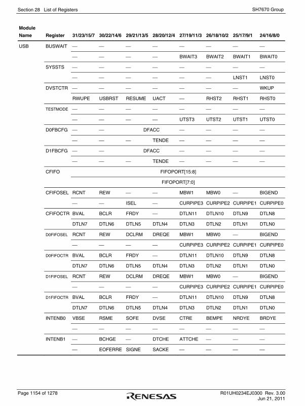
Section 28 List of Registers
Page 1154 of 1278 R01UH0234EJ0300 Rev. 3.00 Jun 21, 2011
SH7670 Group
Module
Name Register 31/23/15/7 30/22/14/6 29/21/13/5 28/20/12/4 27/19/11/3 26/18/10/2 25/17/9/1 24/16/8/0
USB BUSWAIT ⎯ ⎯ ⎯ ⎯ ⎯ ⎯ ⎯ ⎯
⎯ ⎯ ⎯ ⎯ BWAIT3 BWAIT2 BWAIT1 BWAIT0
SYSSTS ⎯ ⎯ ⎯ ⎯ ⎯ ⎯ ⎯ ⎯
⎯ ⎯ ⎯ ⎯ ⎯ ⎯ LNST1 LNST0
DVSTCTR ⎯ ⎯ ⎯ ⎯ ⎯ ⎯ ⎯ WKUP
RWUPE USBRST RESUME UACT ⎯ RHST2 RHST1 RHST0
TESTMODE ⎯ ⎯ ⎯ ⎯ ⎯ ⎯ ⎯ ⎯
⎯ ⎯ ⎯ ⎯ UTST3 UTST2 UTST1 UTST0
D0FBCFG ⎯ ⎯ DFACC ⎯ ⎯ ⎯ ⎯
⎯ ⎯ ⎯ TENDE ⎯ ⎯ ⎯ ⎯
D1FBCFG ⎯ ⎯ DFACC ⎯ ⎯ ⎯ ⎯
⎯ ⎯ ⎯ TENDE ⎯ ⎯ ⎯ ⎯
CFIFO FIFOPORT[15:8]
FIFOPORT[7:0]
CFIFOSEL RCNT REW ⎯ ⎯ MBW1 MBW0 ⎯ BIGEND
⎯ ⎯ ISEL ⎯ CURPIPE3 CURPIPE2 CURPIPE1 CURPIPE0
CFIFOCTR BVAL BCLR FRDY ⎯ DTLN11 DTLN10 DTLN9 DTLN8
DTLN7 DTLN6 DTLN5 DTLN4 DTLN3 DTLN2 DTLN1 DTLN0
D0FIFOSEL RCNT REW DCLRM DREQE MBW1 MBW0 ⎯ BIGEND
⎯ ⎯ ⎯ ⎯ CURPIPE3 CURPIPE2 CURPIPE1 CURPIPE0
D0FIFOCTR BVAL BCLR FRDY ⎯ DTLN11 DTLN10 DTLN9 DTLN8
DTLN7 DTLN6 DTLN5 DTLN4 DTLN3 DTLN2 DTLN1 DTLN0
D1FIFOSEL RCNT REW DCLRM DREQE MBW1 MBW0 ⎯ BIGEND
⎯ ⎯ ⎯ ⎯ CURPIPE3 CURPIPE2 CURPIPE1 CURPIPE0
D1FIFOCTR BVAL BCLR FRDY ⎯ DTLN11 DTLN10 DTLN9 DTLN8
DTLN7 DTLN6 DTLN5 DTLN4 DTLN3 DTLN2 DTLN1 DTLN0
INTENB0 VBSE RSME SOFE DVSE CTRE BEMPE NRDYE BRDYE
⎯ ⎯ ⎯ ⎯ ⎯ ⎯ ⎯ ⎯
INTENB1 ⎯ BCHGE ⎯ DTCHE ATTCHE ⎯ ⎯ ⎯
⎯ EOFERRE SIGNE SACKE ⎯ ⎯ ⎯ ⎯
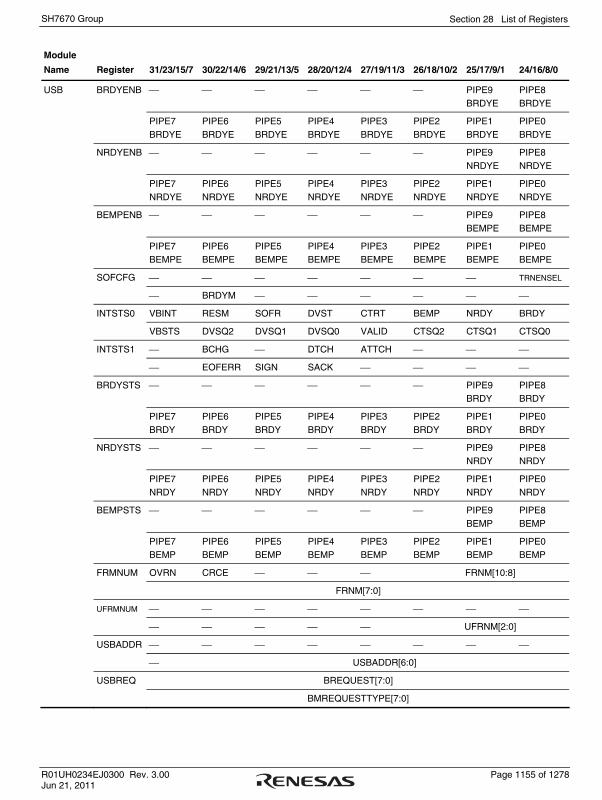
Section 28 List of Registers
R01UH0234EJ0300 Rev. 3.00 Page 1155 of 1278 Jun 21, 2011
SH7670 Group
Module
Name Register 31/23/15/7 30/22/14/6 29/21/13/5 28/20/12/4 27/19/11/3 26/18/10/2 25/17/9/1 24/16/8/0
USB BRDYENB ⎯ ⎯ ⎯ ⎯ ⎯ ⎯ PIPE9 BRDYE
PIPE8 BRDYE
PIPE7 BRDYE
PIPE6 BRDYE
PIPE5 BRDYE
PIPE4 BRDYE
PIPE3 BRDYE
PIPE2 BRDYE
PIPE1 BRDYE
PIPE0 BRDYE
NRDYENB ⎯ ⎯ ⎯ ⎯ ⎯ ⎯ PIPE9 NRDYE
PIPE8 NRDYE
PIPE7 NRDYE
PIPE6 NRDYE
PIPE5 NRDYE
PIPE4 NRDYE
PIPE3 NRDYE
PIPE2 NRDYE
PIPE1 NRDYE
PIPE0 NRDYE
BEMPENB ⎯ ⎯ ⎯ ⎯ ⎯ ⎯ PIPE9 BEMPE
PIPE8 BEMPE
PIPE7 BEMPE
PIPE6 BEMPE
PIPE5 BEMPE
PIPE4 BEMPE
PIPE3 BEMPE
PIPE2 BEMPE
PIPE1 BEMPE
PIPE0 BEMPE
SOFCFG ⎯ ⎯ ⎯ ⎯ ⎯ ⎯ ⎯ TRNENSEL
⎯ BRDYM ⎯ ⎯ ⎯ ⎯ ⎯ ⎯
INTSTS0 VBINT RESM SOFR DVST CTRT BEMP NRDY BRDY
VBSTS DVSQ2 DVSQ1 DVSQ0 VALID CTSQ2 CTSQ1 CTSQ0
INTSTS1 ⎯ BCHG ⎯ DTCH ATTCH ⎯ ⎯ ⎯
⎯ EOFERR SIGN SACK ⎯ ⎯ ⎯ ⎯
BRDYSTS ⎯ ⎯ ⎯ ⎯ ⎯ ⎯ PIPE9 BRDY
PIPE8 BRDY
PIPE7 BRDY
PIPE6 BRDY
PIPE5 BRDY
PIPE4 BRDY
PIPE3 BRDY
PIPE2 BRDY
PIPE1 BRDY
PIPE0 BRDY
NRDYSTS ⎯ ⎯ ⎯ ⎯ ⎯ ⎯ PIPE9 NRDY
PIPE8 NRDY
PIPE7 NRDY
PIPE6 NRDY
PIPE5 NRDY
PIPE4 NRDY
PIPE3 NRDY
PIPE2 NRDY
PIPE1 NRDY
PIPE0 NRDY
BEMPSTS ⎯ ⎯ ⎯ ⎯ ⎯ ⎯ PIPE9 BEMP
PIPE8 BEMP
PIPE7 BEMP
PIPE6 BEMP
PIPE5 BEMP
PIPE4 BEMP
PIPE3 BEMP
PIPE2 BEMP
PIPE1 BEMP
PIPE0 BEMP
FRMNUM OVRN CRCE ⎯ ⎯ ⎯ FRNM[10:8]
FRNM[7:0]
UFRMNUM ⎯ ⎯ ⎯ ⎯ ⎯ ⎯ ⎯ ⎯
⎯ ⎯ ⎯ ⎯ ⎯ UFRNM[2:0]
USBADDR ⎯ ⎯ ⎯ ⎯ ⎯ ⎯ ⎯ ⎯
⎯ USBADDR[6:0]
USBREQ BREQUEST[7:0]
BMREQUESTTYPE[7:0]

Section 28 List of Registers
Page 1156 of 1278 R01UH0234EJ0300 Rev. 3.00 Jun 21, 2011
SH7670 Group
Module
Name Register 31/23/15/7 30/22/14/6 29/21/13/5 28/20/12/4 27/19/11/3 26/18/10/2 25/17/9/1 24/16/8/0
USB USBVAL WVALUE[15:8]
WVALUE[7:0]
USBINDX WINDEX[15:8]
WINDEX[7:0]
USBLENG WLENGTH[15:8]
WLENGTH[7:0]
DCPCFG ⎯ ⎯ ⎯ ⎯ ⎯ ⎯ ⎯ ⎯
⎯ ⎯ ⎯ DIR ⎯ ⎯ ⎯ ⎯
DCPMAXP DEVSEL3 DEVSEL2 DEVSEL1 DEVSEL0 ⎯ ⎯ ⎯ ⎯
⎯ MXPS6 MXPS5 MXPS4 MXPS3 MXPS2 MXPS1 MXPS0
DCPCTR BSTS SUREQ CSCLR CSSTS SUREQCLR ⎯ ⎯ SQCLR
SQSET SQMON PBUSY PINGE ⎯ CCPL PID1 PID0
PIPESEL ⎯ ⎯ ⎯ ⎯ ⎯ ⎯ ⎯ ⎯
⎯ ⎯ ⎯ ⎯ PIPESEL3 PIPESEL2 PIPESEL1 PIPESEL0
PIPECFG TYPE1 TYPE0 ⎯ ⎯ ⎯ BFRE DBLB CNTMD
SHTNAK ⎯ ⎯ DIR EPNUM3 EPNUM2 EPNUM1 EPNUM0
PIPEBUF ⎯ BUFSIZE[4:0] ⎯ ⎯
BUFNMB[7:0]
PIPEMAXP DEVSEL[3:0] ⎯ MXPS[10:8]
MXPS[7:0]
PIPEPERI ⎯ ⎯ ⎯ IFIS ⎯ ⎯ ⎯ ⎯
⎯ ⎯ ⎯ ⎯ ⎯ IITV2 IITV1 IITV0
PIPE1CTR BSTS INBUFM CSCLR CSSTS ⎯ ATREPM ACLRM SQCLR
SQSET SQMON PBUSY ⎯ ⎯ ⎯ PID1 PID0
PIPE2CTR BSTS INBUFM CSCLR CSSTS ⎯ ATREPM ACLRM SQCLR
SQSET SQMON PBUSY ⎯ ⎯ ⎯ PID1 PID0
PIPE3CTR BSTS INBUFM CSCLR CSSTS ⎯ ATREPM ACLRM SQCLR
SQSET SQMON PBUSY ⎯ ⎯ ⎯ PID1 PID0
PIPE4CTR BSTS INBUFM CSCLR CSSTS ⎯ ATREPM ACLRM SQCLR
SQSET SQMON PBUSY ⎯ ⎯ ⎯ PID1 PID0
PIPE5CTR BSTS INBUFM CSCLR CSSTS ⎯ ATREPM ACLRM SQCLR
SQSET SQMON PBUSY ⎯ ⎯ ⎯ PID1 PID0

Section 28 List of Registers
R01UH0234EJ0300 Rev. 3.00 Page 1157 of 1278 Jun 21, 2011
SH7670 Group
Module
Name Register 31/23/15/7 30/22/14/6 29/21/13/5 28/20/12/4 27/19/11/3 26/18/10/2 25/17/9/1 24/16/8/0
USB PIPE6CTR BSTS ⎯ CSCLR CSSTS ⎯ ⎯ ACLRM SQCLR
SQSET SQMON PBUSY ⎯ ⎯ ⎯ PID1 PID0
PIPE7CTR BSTS ⎯ CSCLR CSSTS ⎯ ⎯ ACLRM SQCLR
SQSET SQMON PBUSY ⎯ ⎯ ⎯ PID1 PID0
PIPE8CTR BSTS ⎯ CSCLR CSSTS ⎯ ⎯ ACLRM SQCLR
SQSET SQMON PBUSY ⎯ ⎯ ⎯ PID1 PID0
PIPE9CTR BSTS ⎯ CSCLR CSSTS ⎯ ⎯ ACLRM SQCLR
SQSET SQMON PBUSY ⎯ ⎯ ⎯ PID1 PID0
PIPE1TRE ⎯ ⎯ ⎯ ⎯ ⎯ ⎯ TRENB TRCLR
⎯ ⎯ ⎯ ⎯ ⎯ ⎯ ⎯ ⎯
PIPE1TRN TRNCNT[15:8]
TRNCNT[7:0]
PIPE2TRE ⎯ ⎯ ⎯ ⎯ ⎯ ⎯ TRENB TRCLR
⎯ ⎯ ⎯ ⎯ ⎯ ⎯ ⎯ ⎯
PIPE2TRN TRNCNT[15:8]
TRNCNT[7:0]
PIPE3TRE ⎯ ⎯ ⎯ ⎯ ⎯ ⎯ TRENB TRCLR
⎯ ⎯ ⎯ ⎯ ⎯ ⎯ ⎯ ⎯
PIPE3TRN TRNCNT[15:8]
TRNCNT[7:0]
PIPE4TRE ⎯ ⎯ ⎯ ⎯ ⎯ ⎯ TRENB TRCLR
⎯ ⎯ ⎯ ⎯ ⎯ ⎯ ⎯ ⎯
PIPE4TRN TRNCNT[15:8]
TRNCNT[7:0]
PIPE5TRE ⎯ ⎯ ⎯ ⎯ ⎯ ⎯ TRENB TRCLR
⎯ ⎯ ⎯ ⎯ ⎯ ⎯ ⎯ ⎯
PIPE5TRN TRNCNT[15:8]
TRNCNT[7:0]
DEVADD0 ⎯ UPPHUB[3:0] HUBPORT[2:0]
USBSPD[1:0] ⎯ ⎯ ⎯ ⎯ ⎯ ⎯

Section 28 List of Registers
Page 1158 of 1278 R01UH0234EJ0300 Rev. 3.00 Jun 21, 2011
SH7670 Group
Module
Name Register 31/23/15/7 30/22/14/6 29/21/13/5 28/20/12/4 27/19/11/3 26/18/10/2 25/17/9/1 24/16/8/0
USB DEVADD1 ⎯ UPPHUB[3:0] HUBPORT[2:0]
USBSPD[1:0] ⎯ ⎯ ⎯ ⎯ ⎯ ⎯
DEVADD2 ⎯ UPPHUB[3:0] HUBPORT[2:0]
USBSPD[1:0] ⎯ ⎯ ⎯ ⎯ ⎯ ⎯
DEVADD3 ⎯ UPPHUB[3:0] HUBPORT[2:0]
USBSPD[1:0] ⎯ ⎯ ⎯ ⎯ ⎯ ⎯
DEVADD4 ⎯ UPPHUB[3:0] HUBPORT[2:0]
USBSPD[1:0] ⎯ ⎯ ⎯ ⎯ ⎯ ⎯
DEVADD5 ⎯ UPPHUB[3:0] HUBPORT[2:0]
USBSPD[1:0] ⎯ ⎯ ⎯ ⎯ ⎯ ⎯
DEVADD6 ⎯ UPPHUB[3:0] HUBPORT[2:0]
USBSPD[1:0] ⎯ ⎯ ⎯ ⎯ ⎯ ⎯
DEVADD7 ⎯ UPPHUB[3:0] HUBPORT[2:0]
USBSPD[1:0] ⎯ ⎯ ⎯ ⎯ ⎯ ⎯
DEVADD8 ⎯ UPPHUB[3:0] HUBPORT[2:0]
USBSPD[1:0] ⎯ ⎯ ⎯ ⎯ ⎯ ⎯
DEVADD9 ⎯ UPPHUB[3:0] HUBPORT[2:0]
USBSPD[1:0] ⎯ ⎯ ⎯ ⎯ ⎯ ⎯
DEVADDA ⎯ UPPHUB[3:0] HUBPORT[2:0]
USBSPD[1:0] ⎯ ⎯ ⎯ ⎯ ⎯ ⎯
IIC3 ICCR1_0 ICE RCVD MST TRS CKS3 CKS2 CKS1 CKS0
ICCR2_0 BBSY SCP SDAO SDAOP SCLO ⎯ IIRST ⎯
ICMR_0 MLS ⎯ ⎯ ⎯ BCWP BC2 BC1 BC0
ICIER_0 TIE TEIE RIE NAKIE STIE ACKE ACKBR ACKBT
ICSR_0 TDRE TEND RDRF NACKF STOP AL/OVE AAS ADZ
SAR_0 SVA6 SVA5 SVA4 SVA3 SVA2 SVA1 SVA0 FS
ICDRT_0
ICDRR_0
NF2CYC_0 ⎯ ⎯ ⎯ ⎯ ⎯ ⎯ PRS NF2CYC

Section 28 List of Registers
R01UH0234EJ0300 Rev. 3.00 Page 1159 of 1278 Jun 21, 2011
SH7670 Group
Module
Name Register 31/23/15/7 30/22/14/6 29/21/13/5 28/20/12/4 27/19/11/3 26/18/10/2 25/17/9/1 24/16/8/0
HIF HIFIDX ⎯ ⎯ ⎯ ⎯ ⎯ ⎯ ⎯ ⎯
⎯ ⎯ ⎯ ⎯ ⎯ ⎯ ⎯ ⎯
⎯ ⎯ ⎯ ⎯ ⎯ ⎯ ⎯ ⎯
REG5 REG4 REG3 REG2 REG1 REG0 BYTE1 BYTE0
HIFGSR ⎯ ⎯ ⎯ ⎯ ⎯ ⎯ ⎯ ⎯
⎯ ⎯ ⎯ ⎯ ⎯ ⎯ ⎯ ⎯
STATUS15 STATUS14 STATUS13 STATUS12 STATUS11 STATUS10 STATUS9 STATUS8
STATUS7 STATUS6 STATUS5 STATUS4 STATUS3 STATUS2 STATUS1 STATUS0
HIFSCR ⎯ ⎯ ⎯ ⎯ ⎯ ⎯ ⎯ ⎯
⎯ ⎯ ⎯ ⎯ ⎯ ⎯ ⎯ ⎯
⎯ ⎯ ⎯ ⎯ DMD DPOL BMD BSEL
⎯ ⎯ MD1 ⎯ ⎯ WBSWP EDN BO
HIFMCR ⎯ ⎯ ⎯ ⎯ ⎯ ⎯ ⎯ ⎯
⎯ ⎯ ⎯ ⎯ ⎯ ⎯ ⎯ ⎯
⎯ ⎯ ⎯ ⎯ ⎯ ⎯ ⎯ ⎯
LOCK ⎯ WT ⎯ RD ⎯ ⎯ AI/AD
HIFIICR ⎯ ⎯ ⎯ ⎯ ⎯ ⎯ ⎯ ⎯
⎯ ⎯ ⎯ ⎯ ⎯ ⎯ ⎯ ⎯
⎯ ⎯ ⎯ ⎯ ⎯ ⎯ ⎯ ⎯
IIC6 IIC5 IIC4 IIC3 IIC2 IIC1 IIC0 IIR
HIFEICR ⎯ ⎯ ⎯ ⎯ ⎯ ⎯ ⎯ ⎯
⎯ ⎯ ⎯ ⎯ ⎯ ⎯ ⎯ ⎯
⎯ ⎯ ⎯ ⎯ ⎯ ⎯ ⎯ ⎯
EIC6 EIC5 EIC4 EIC3 EIC2 EIC1 EIC0 EIR
HIFADR ⎯ ⎯ ⎯ ⎯ ⎯ ⎯ ⎯ ⎯
⎯ ⎯ ⎯ ⎯ ⎯ ⎯ ⎯ ⎯
⎯ ⎯ ⎯ ⎯ ⎯ ⎯ A9 A8
A7 A6 A5 A4 A3 A2 ⎯ ⎯

Section 28 List of Registers
Page 1160 of 1278 R01UH0234EJ0300 Rev. 3.00 Jun 21, 2011
SH7670 Group
Module
Name Register 31/23/15/7 30/22/14/6 29/21/13/5 28/20/12/4 27/19/11/3 26/18/10/2 25/17/9/1 24/16/8/0
HIF HIFDATA D31 D30 D29 D28 D27 D26 D25 D24
D23 D22 D21 D20 D19 D18 D17 D16
D15 D14 D13 D12 D11 D10 D9 D8
D7 D6 D5 D4 D3 D2 D1 D0
HIFDTR ⎯ ⎯ ⎯ ⎯ ⎯ ⎯ ⎯ ⎯
⎯ ⎯ ⎯ ⎯ ⎯ ⎯ ⎯ ⎯
⎯ ⎯ ⎯ ⎯ ⎯ ⎯ ⎯ ⎯
⎯ ⎯ ⎯ ⎯ ⎯ ⎯ ⎯ DTRG
HIFBICR ⎯ ⎯ ⎯ ⎯ ⎯ ⎯ ⎯ ⎯
⎯ ⎯ ⎯ ⎯ ⎯ ⎯ ⎯ ⎯
⎯ ⎯ ⎯ ⎯ ⎯ ⎯ ⎯ ⎯
⎯ ⎯ ⎯ ⎯ ⎯ ⎯ BIE BIF
HIFBCR ⎯ ⎯ ⎯ ⎯ ⎯ ⎯ ⎯ ⎯
⎯ ⎯ ⎯ ⎯ ⎯ ⎯ ⎯ ⎯
⎯ ⎯ ⎯ ⎯ ⎯ ⎯ ⎯ ⎯
⎯ ⎯ ⎯ ⎯ ⎯ ⎯ ⎯ AC
CMT CMSTR ⎯ ⎯ ⎯ ⎯ ⎯ ⎯ ⎯ ⎯
⎯ ⎯ ⎯ ⎯ ⎯ ⎯ STR1 STR0
CMCSR_0 ⎯ ⎯ ⎯ ⎯ ⎯ ⎯ ⎯ ⎯
CMF CMIE ⎯ ⎯ ⎯ ⎯ CKS1 CKS0
CMCNT_0 Bit 15 Bit 14 Bit 13 Bit 12 Bit 11 Bit 10 Bit 9 Bit 8
Bit 7 Bit 6 Bit 5 Bit 4 Bit 3 Bit 2 Bit 1 Bit 0
CMCOR_0 Bit 15 Bit 14 Bit 13 Bit 12 Bit 11 Bit 10 Bit 9 Bit 8
Bit 7 Bit 6 Bit 5 Bit 4 Bit 3 Bit 2 Bit 1 Bit 0
CMCSR_1 ⎯ ⎯ ⎯ ⎯ ⎯ ⎯ ⎯ ⎯
CMF CMIE ⎯ ⎯ ⎯ ⎯ CKS1 CKS0
CMCNT_1 Bit 15 Bit 14 Bit 13 Bit 12 Bit 11 Bit 10 Bit 9 Bit 8
Bit 7 Bit 6 Bit 5 Bit 4 Bit 3 Bit 2 Bit 1 Bit 0
CMCOR_1 Bit 15 Bit 14 Bit 13 Bit 12 Bit 11 Bit 10 Bit 9 Bit 8
Bit 7 Bit 6 Bit 5 Bit 4 Bit 3 Bit 2 Bit 1 Bit 0

Section 28 List of Registers
R01UH0234EJ0300 Rev. 3.00 Page 1161 of 1278 Jun 21, 2011
SH7670 Group
Module
Name Register 31/23/15/7 30/22/14/6 29/21/13/5 28/20/12/4 27/19/11/3 26/18/10/2 25/17/9/1 24/16/8/0
SCIF0 SCSMR_0 ⎯ ⎯ ⎯ ⎯ ⎯ ⎯ ⎯ ⎯
C/A CHR PE O/E STOP ⎯ CKS1 CKS0
SCBRR_0 Bit 7 Bit 6 Bit 5 Bit 4 Bit 3 Bit 2 Bit 1 Bit 0
SCSCR_0 ⎯ ⎯ ⎯ ⎯ ⎯ ⎯ ⎯ ⎯
TIE RIE TE RE REIE ⎯ CKE1 CKE0
SCFTDR_0 Bit 7 Bit 6 Bit 5 Bit 4 Bit 3 Bit 2 Bit 1 Bit 0
SCFSR_0 PER3 PER2 PER1 PER0 FER3 FER2 FER1 FER0
ER TEND TDFE BRK FER PER RDF DR
SCFRDR_0 Bit 7 Bit 6 Bit 5 Bit 4 Bit 3 Bit 2 Bit 1 Bit 0
SCFCR_0 ⎯ ⎯ ⎯ ⎯ ⎯ RSTRG2 RSTRG1 RSTRG0
RTRG1 RTRG0 TTRG1 TTRG0 MCE TFRST RFRST LOOP
SCFDR_0 ⎯ ⎯ ⎯ T4 T3 T2 T1 T0
⎯ ⎯ ⎯ R4 R3 R2 R1 R0
⎯ ⎯ ⎯ ⎯ ⎯ ⎯ ⎯ ⎯
SCSPTR_
0 RTSIO RTSDT CTSIO CTSDT SCKIO SCKDT SPB2IO SPB2DT
SCLSR_0 ⎯ ⎯ ⎯ ⎯ ⎯ ⎯ ⎯ ⎯
⎯ ⎯ ⎯ ⎯ ⎯ ⎯ ⎯ ORER
SCIF1 SCSMR_1 ⎯ ⎯ ⎯ ⎯ ⎯ ⎯ ⎯ ⎯
C/A CHR PE O/E STOP ⎯ CKS1 CKS0
SCBRR_1 Bit 7 Bit 6 Bit 5 Bit 4 Bit 3 Bit 2 Bit 1 Bit 0
SCSCR_1 ⎯ ⎯ ⎯ ⎯ ⎯ ⎯ ⎯ ⎯
TIE RIE TE RE REIE ⎯ CKE1 CKE0
SCFTDR_1 Bit 7 Bit 6 Bit 5 Bit 4 Bit 3 Bit 2 Bit 1 Bit 0
SCFSR_1 PER3 PER2 PER1 PER0 FER3 FER2 FER1 FER0
ER TEND TDFE BRK FER PER RDF DR
SCFRDR_1 Bit 7 Bit 6 Bit 5 Bit 4 Bit 3 Bit 2 Bit 1 Bit 0
SCFCR_1 ⎯ ⎯ ⎯ ⎯ ⎯ RSTRG2 RSTRG1 RSTRG0
RTRG1 RTRG0 TTRG1 TTRG0 MCE TFRST RFRST LOOP
SCFDR_1 ⎯ ⎯ ⎯ T4 T3 T2 T1 T0
⎯ ⎯ ⎯ R4 R3 R2 R1 R0

Section 28 List of Registers
Page 1162 of 1278 R01UH0234EJ0300 Rev. 3.00 Jun 21, 2011
SH7670 Group
Module
Name Register 31/23/15/7 30/22/14/6 29/21/13/5 28/20/12/4 27/19/11/3 26/18/10/2 25/17/9/1 24/16/8/0
SCIF1 ⎯ ⎯ ⎯ ⎯ ⎯ ⎯ ⎯ ⎯
SCSPTR_
1 RTSIO RTSDT CTSIO CTSDT SCKIO SCKDT SPB2IO SPB2DT
SCLSR_1 ⎯ ⎯ ⎯ ⎯ ⎯ ⎯ ⎯ ⎯
⎯ ⎯ ⎯ ⎯ ⎯ ⎯ ⎯ ORER
SCIF2 SCSMR_2 ⎯ ⎯ ⎯ ⎯ ⎯ ⎯ ⎯ ⎯
C/A CHR PE O/E STOP ⎯ CKS1 CKS0
SCBRR_2 Bit 7 Bit 6 Bit 5 Bit 4 Bit 3 Bit 2 Bit 1 Bit 0
SCSCR_2 ⎯ ⎯ ⎯ ⎯ ⎯ ⎯ ⎯ ⎯
TIE RIE TE RE REIE ⎯ CKE1 CKE0
SCFTDR_2 Bit 7 Bit 6 Bit 5 Bit 4 Bit 3 Bit 2 Bit 1 Bit 0
SCFSR_2 PER3 PER2 PER1 PER0 FER3 FER2 FER1 FER0
ER TEND TDFE BRK FER PER RDF DR
SCFRDR_2 Bit 7 Bit 6 Bit 5 Bit 4 Bit 3 Bit 2 Bit 1 Bit 0
SCFCR_2 ⎯ ⎯ ⎯ ⎯ ⎯ RSTRG2 RSTRG1 RSTRG0
RTRG1 RTRG0 TTRG1 TTRG0 MCE TFRST RFRST LOOP
SCFDR_2 ⎯ ⎯ ⎯ T4 T3 T2 T1 T0
⎯ ⎯ ⎯ R4 R3 R2 R1 R0
⎯ ⎯ ⎯ ⎯ ⎯ ⎯ ⎯ ⎯
SCSPTR_
2 RTSIO RTSDT CTSIO CTSDT SCKIO SCKDT SPB2IO SPB2DT
SCLSR_2 ⎯ ⎯ ⎯ ⎯ ⎯ ⎯ ⎯ ⎯
⎯ ⎯ ⎯ ⎯ ⎯ ⎯ ⎯ ORER
I/O PADRH ⎯ ⎯ ⎯ ⎯ ⎯ ⎯ PA25DR PA24DR
PA23DR PA22DR PA21DR PA20DR PA19DR PA18DR PA17DR ⎯
PAIORH ⎯ ⎯ ⎯ ⎯ ⎯ ⎯ PA25IOR PA24IOR
PA23IOR PA22IOR PA21IOR PA20IOR PA19IOR PA18IOR PA17IOR ⎯
PACRH2 ⎯ ⎯ ⎯ ⎯ ⎯ ⎯ ⎯ ⎯
⎯ ⎯ ⎯ ⎯ ⎯ PA25MD0 ⎯ PA24MD0
PACRH1 ⎯ PA23MD0 ⎯ PA22MD0 ⎯ PA21MD0 ⎯ PA20MD0
⎯ PA19MD0 ⎯ PA18MD0 ⎯ PA17MD0 ⎯ ⎯
PBDRL ⎯ ⎯ ⎯ ⎯ ⎯ ⎯ ⎯ ⎯
PB7DR PB6DR PB5DR PB4DR PB3DR PB2DR PB1DR PB0DR

Section 28 List of Registers
R01UH0234EJ0300 Rev. 3.00 Page 1163 of 1278 Jun 21, 2011
SH7670 Group
Module
Name Register 31/23/15/7 30/22/14/6 29/21/13/5 28/20/12/4 27/19/11/3 26/18/10/2 25/17/9/1 24/16/8/0
I/O PBIORL ⎯ ⎯ ⎯ ⎯ ⎯ ⎯ ⎯ ⎯
PB7IOR PB6IOR PB5IOR PB4IOR PB3IOR PB2IOR PB1IOR PB0IOR
PBCRL1 ⎯ PB7MD0 ⎯ PB6MD0 PB5MD1 PB5MD0 PB4MD1 PB4MD0
PB3MD1 PB3MD0 PB2MD1 PB2MD0 PB1MD1 PB1MD0 PB0MD1 PB0MD0
PCDRH ⎯ ⎯ ⎯ ⎯ ⎯ ⎯ ⎯ ⎯
⎯ ⎯ ⎯ PC20DR PC19DR PC18DR PC17DR PC16DR
PCDRL PC15DR PC14DR PC13DR PC12DR PC11DR PC10DR PC9DR PC8DR
PC7DR PC6DR PC5DR PC4DR PC3DR PC2DR PC1DR PC0DR
PCIORH ⎯ ⎯ ⎯ ⎯ ⎯ ⎯ ⎯ ⎯
⎯ ⎯ ⎯ PC20IOR PC19IOR PC18IOR PC17IOR PC16IOR
PCIORL PC15IOR PC14IOR PC13IOR PC12IOR PC11IOR PC10IOR PC9IOR PC8IOR
PC7IOR PC6IOR PC5IOR PC4IOR PC3IOR PC2IOR PC1IOR PC0IOR
PCCRH1 ⎯ ⎯ ⎯ ⎯ ⎯ ⎯ ⎯ PC20MD0
⎯ PC19MD0 ⎯ PC18MD0 ⎯ PC17MD0 ⎯ PC16MD0
PCCRL2 ⎯ PC15MD0 ⎯ PC14MD0 ⎯ PC13MD0 ⎯ PC12MD0
⎯ PC11MD0 ⎯ PC10MD0 ⎯ PC9MD0 ⎯ PC8MD0
PCCRL1 ⎯ PC7MD0 ⎯ PC6MD0 ⎯ PC5MD0 ⎯ PC4MD0
⎯ PC3MD0 ⎯ PC2MD0 ⎯ PC1MD0 ⎯ PC0MD0
PDDRL ⎯ ⎯ ⎯ ⎯ ⎯ ⎯ ⎯ ⎯
PD7DR PD6DR PD5DR PD4DR PD3DR PD2DR PD1DR PD0DR
PDIORL ⎯ ⎯ ⎯ ⎯ ⎯ ⎯ ⎯ ⎯
PD7IOR PD6IOR PD5IOR PD4IOR PD3IOR PD2IOR PD1IOR PD0IOR
PDCRL1 PD7MD1 PD7MD0 PD6MD1 PD6MD0 PD5MD1 PD5MD0 PD4MD1 PD4MD0
PD3MD1 PD3MD0 PD2MD1 PD2MD0 PD1MD1 PD1MD0 PD0MD1 PD0MD0
PEDRL ⎯ ⎯ ⎯ ⎯ PE11DR PE10DR PE9DR PE8DR
PE7DR PE6DR PE5DR PE4DR PE3DR PE2DR PE1DR PE0DR
PEIORL ⎯ ⎯ ⎯ ⎯ PE11IOR PE10IOR PE9IOR PE8IOR
PE7IOR PE6IOR PE5IOR PE4IOR PE3IOR PE2IOR PE1IOR PE0IOR
PECRL2 ⎯ ⎯ ⎯ ⎯ PE13MD1 PE13MD0 PE12MD1 PE12MD0
PE11MD1 PE11MD0 PE10MD1 PE10MD0 PE09MD1 PE09MD0 PE08MD1 PE08MD0

Section 28 List of Registers
Page 1164 of 1278 R01UH0234EJ0300 Rev. 3.00 Jun 21, 2011
SH7670 Group
Module
Name Register 31/23/15/7 30/22/14/6 29/21/13/5 28/20/12/4 27/19/11/3 26/18/10/2 25/17/9/1 24/16/8/0
I/O PECRL1 PE07MD1 PE07MD0 PE06MD1 PE06MD0 PE05MD1 PE05MD0 PE04MD1 PE04MD0
PE03MD1 PE03MD0 PE02MD1 PE02MD0 PE01MD1 PE01MD0 PE00MD1 PE00MD0
PFDRL ⎯ ⎯ ⎯ ⎯ PF11DR PF10DR PF9DR PF8DR
PF7DR PF6DR PF5DR PF4DR PF3DR PF2DR PF1DR PF0DR
PFIORL ⎯ ⎯ ⎯ ⎯ PF11IOR PF10IOR PF9IOR PF8IOR
PF7IOR PF6IOR PF5IOR PF4IOR PF3IOR PF2IOR PF1IOR PF0IOR
PFCRL2 ⎯ ⎯ ⎯ ⎯ PF13MD1 PF13MD0 ⎯ ⎯
PF11MD1 PF11MD0 PF10MD1 PF10MD0 PF09MD1 PF09MD0 ⎯ PF08MD0
PFCRL1 PF07MD1 PF07MD0 PF06MD1 PF06MD0 PF05MD1 PF05MD0 PF04MD1 PF04MD0
PF03MD1 PF03MD0 PF02MD1 PF02MD0 PF01MD1 PF01MD0 ⎯ PF00MD0
PGDRH ⎯ ⎯ ⎯ ⎯ ⎯ ⎯ ⎯ ⎯
PG23DR PG22DR PG21DR PG20DR PG19DR PG18DR PG17DR PG16DR
PGDRL PG15DR PG14DR PG13DR PG12DR PG11DR PG10DR PG9DR PG8DR
PG7DR PG6DR PG5DR PG4DR PG3DR PG2DR PG1DR PG0DR
PGIORH ⎯ ⎯ ⎯ ⎯ ⎯ ⎯ ⎯ ⎯
PG23IOR PG22IOR PG21IOR PG20IOR PG19IOR PG18IOR PG17IOR PG16IOR
PGIORL PG15IOR PG14IOR PG13IOR PG12IOR PG11IOR PG10IOR PG9IOR PG8IOR
PG7IOR PG6IOR PG5IOR PG4IOR PG3IOR PG2IOR PG1IOR PG0IOR
PGCRH2 ⎯ PG23MD0 ⎯ PG22MD0 ⎯ PG21MD0 ⎯ PG20MD0
⎯ PG19MD0 ⎯ PG18MD0 ⎯ PG17MD0 ⎯ PG16MD0
PGCRL2 ⎯ PG15MD0 ⎯ PG14MD0 ⎯ PG13MD0 ⎯ PG12MD0
⎯ PG11MD0 ⎯ PG10MD0 ⎯ PG09MD0 ⎯ PG08MD0
PGCRL1 ⎯ PG07MD0 ⎯ PG06MD0 ⎯ PG05MD0 ⎯ PG04MD0
⎯ PG03MD0 ⎯ PG02MD0 ⎯ PG01MD0 ⎯ PG00MD0
UBC BAR_0 BA31 BA30 BA29 BA28 BA27 BA26 BA25 BA24
BA23 BA22 BA21 BA20 BA19 BA18 BA17 BA16
BA15 BA14 BA13 BA12 BA11 BA10 BA9 BA8
BA7 BA6 BA5 BA4 BA3 BA2 BA1 BA0

Section 28 List of Registers
R01UH0234EJ0300 Rev. 3.00 Page 1165 of 1278 Jun 21, 2011
SH7670 Group
Module
Name Register 31/23/15/7 30/22/14/6 29/21/13/5 28/20/12/4 27/19/11/3 26/18/10/2 25/17/9/1 24/16/8/0
UBC BAMR_0 BAM31 BAM30 BAM29 BAM28 BAM27 BAM26 BAM25 BAM24
BAM23 BAM22 BAM21 BAM20 BAM19 BAM18 BAM17 BAM16
BAM15 BAM14 BAM13 BAM12 BAM11 BAM10 BAM9 BAM8
BAM7 BAM6 BAM5 BAM4 BAM3 BAM2 BAM1 BAM0
BDR_0 BD31 BD30 BD29 BD28 BD27 BD26 BD25 BD24
BD23 BD22 BD21 BD20 BD19 BD18 BD17 BD16
BD15 BD14 BD13 BD12 BD11 BD10 BD9 BD8
BD7 BD6 BD5 BD4 BD3 BD2 BD1 BD0
BDMR_0 BDM31 BDM30 BDM29 BDM28 BDM27 BDM26 BDM25 BDM24
BDM23 BDM22 BDM21 BDM20 BDM19 BDM18 BDM17 BDM16
BDM15 BDM14 BDM13 BDM12 BDM11 BDM10 BDM9 BDM8
BDM7 BDM6 BDM5 BDM4 BDM3 BDM2 BDM1 BDM0
BAR_1 BA31 BA30 BA29 BA28 BA27 BA26 BA25 BA24
BA23 BA22 BA21 BA20 BA19 BA18 BA17 BA16
BA15 BA14 BA13 BA12 BA11 BA10 BA9 BA8
BA7 BA6 BA5 BA4 BA3 BA2 BA1 BA0
BAMR_1 BAM31 BAM30 BAM29 BAM28 BAM27 BAM26 BAM25 BAM24
BAM23 BAM22 BAM21 BAM20 BAM19 BAM18 BAM17 BAM16
BAM15 BAM14 BAM13 BAM12 BAM11 BAM10 BAM9 BAM8
BAM7 BAM6 BAM5 BAM4 BAM3 BAM2 BAM1 BAM0
BDR_1 BD31 BD30 BD29 BD28 BD27 BD26 BD25 BD24
BD23 BD22 BD21 BD20 BD19 BD18 BD17 BD16
BD15 BD14 BD13 BD12 BD11 BD10 BD9 BD8
BD7 BD6 BD5 BD4 BD3 BD2 BD1 BD0
BDMR_1 BDM31 BDM30 BDM29 BDM28 BDM27 BDM26 BDM25 BDM24
BDM23 BDM22 BDM21 BDM20 BDM19 BDM18 BDM17 BDM16
BDM15 BDM14 BDM13 BDM12 BDM11 BDM10 BDM9 BDM8
BDM7 BDM6 BDM5 BDM4 BDM3 BDM2 BDM1 BDM0
BBR_0 ⎯ ⎯ UBID DBE CP3 CP2 CP1 CP0
CD1 CD0 ID1 ID0 RW1 RW0 SZ1 SZ0

Section 28 List of Registers
Page 1166 of 1278 R01UH0234EJ0300 Rev. 3.00 Jun 21, 2011
SH7670 Group
Module
Name Register 31/23/15/7 30/22/14/6 29/21/13/5 28/20/12/4 27/19/11/3 26/18/10/2 25/17/9/1 24/16/8/0
UBC BBR_1 ⎯ ⎯ UBID DBE CP3 CP2 CP1 CP0
CD1 CD0 ID1 ID0 RW1 RW0 SZ1 SZ0
BRCR ⎯ ⎯ ⎯ ⎯ ⎯ ⎯ ⎯ ⎯
⎯ ⎯ ⎯ ⎯ ⎯ ⎯ ⎯ ⎯
SCMFC0 SCMFC1 SCMFD0 SCMFD1 ⎯ ⎯ ⎯ ⎯
⎯ PCB1 PCB0 ⎯ ⎯ ⎯ ⎯ ⎯
H-UDI SDIR TI7 TI6 TI5 TI4 TI3 TI2 TI1 TI0
⎯ ⎯ ⎯ ⎯ ⎯ ⎯ ⎯ ⎯

Section 28 List of Registers
R01UH0234EJ0300 Rev. 3.00 Page 1167 of 1278 Jun 21, 2011
SH7670 Group
28.3 Register States in Each Operating Mode
Module Name
Register Abbreviation Address
Power-on Reset
Software Standby
Module Standby Sleep
Cache CCR1 H'FFFC1000 Initialized Retained Retained Retained
CCR2 H'FFFC1004 Initialized Retained Retained Retained
INTC ICR0 H'FFFE0800 Initialized*1 Retained ⎯*3 Retained
ICR1 H'FFFE0802 Initialized*1 Retained ⎯*3 Retained
IRQRR H'FFFE0806 Initialized Retained ⎯*3 Retained
IBCR H'FFFE080C Initialized Retained ⎯*3 Retained
IBNR H'FFFE080E Initialized Retained ⎯*3 Retained
IPR01 H'FFFE0818 Initialized Retained ⎯*3 Retained
IPR02 H'FFFE081A Initialized Retained ⎯*3 Retained
IPR06 H'FFFE0C00 Initialized Retained ⎯*3 Retained
IPR07 H'FFFE0C02 Initialized Retained ⎯*3 Retained
IPR08 H'FFFE0C04 Initialized Retained ⎯*3 Retained
IPR09 H'FFFE0C06 Initialized Retained ⎯*3 Retained
IPR10 H'FFFE0C08 Initialized Retained ⎯*3 Retained
IPR11 H'FFFE0C0A Initialized Retained ⎯*3 Retained
IPR12 H'FFFE0C0C Initialized Retained ⎯*3 Retained
IPR13 H'FFFE0C0E Initialized Retained ⎯*3 Retained
IPR14 H'FFFE0C10 Initialized Retained ⎯*3 Retained
IPR15 H'FFFE0C12 Initialized Retained ⎯*3 Retained
IPR16 H'FFFE0C14 Initialized Retained ⎯*3 Retained
BSC CMNCR H'FFFC0000 Initialized*1 Retained ⎯*3 Retained
CS0BCR H'FFFC0004 Initialized Retained ⎯*3 Retained
CS3BCR H'FFFC0010 Initialized Retained ⎯*3 Retained
CS4BCR H'FFFC0014 Initialized Retained ⎯*3 Retained
CS5BCR H'FFFC0018 Initialized Retained ⎯*3 Retained
CS6BCR H'FFFC001C Initialized Retained ⎯*3 Retained
CS0WCR H'FFFC0028 Initialized Retained ⎯*3 Retained
CS3WCR H'FFFC0034 Initialized Retained ⎯*3 Retained
CS4WCR H'FFFC0038 Initialized Retained ⎯*3 Retained

Section 28 List of Registers
Page 1168 of 1278 R01UH0234EJ0300 Rev. 3.00 Jun 21, 2011
SH7670 Group
Module Name
Register Abbreviation Address
Power-on Reset
Software Standby
Module Standby Sleep
BSC CS5WCR H'FFFC003C Initialized Retained ⎯*3 Retained
CS6WCR H'FFFC0040 Initialized Retained ⎯*3 Retained
SDCR H'FFFC004C Initialized Retained ⎯*3 Retained
RTCSR H'FFFC0050 Initialized Retained ⎯*3 Retained
RTCNT H'FFFC0054 Initialized Retained ⎯*3 Retained
RTCOR H'FFFC0058 Initialized Retained ⎯*3 Retained
IBMPR H'FFFC1818 Initialized Retained Retained Retained
DMAC SAR_0 H'FFFE1000 Initialized Retained Retained Retained
DAR_0 H'FFFE1004 Initialized Retained Retained Retained
DMATCR_0 H'FFFE1008 Initialized Retained Retained Retained
CHCR_0 H'FFFE100C Initialized Retained Retained Retained
SAR_1 H'FFFE1010 Initialized Retained Retained Retained
DAR_1 H'FFFE1014 Initialized Retained Retained Retained
DMATCR_1 H'FFFE1018 Initialized Retained Retained Retained
CHCR_1 H'FFFE101C Initialized Retained Retained Retained
SAR_2 H'FFFE1020 Initialized Retained Retained Retained
DAR_2 H'FFFE1024 Initialized Retained Retained Retained
DMATCR_2 H'FFFE1028 Initialized Retained Retained Retained
CHCR_2 H'FFFE102C Initialized Retained Retained Retained
SAR_3 H'FFFE1030 Initialized Retained Retained Retained
DAR_3 H'FFFE1034 Initialized Retained Retained Retained
DMATCR_3 H'FFFE1038 Initialized Retained Retained Retained
CHCR_3 H'FFFE103C Initialized Retained Retained Retained
SAR_4 H'FFFE1040 Initialized Retained Retained Retained
DAR_4 H'FFFE1044 Initialized Retained Retained Retained
DMATCR_4 H'FFFE1048 Initialized Retained Retained Retained
CHCR_4 H'FFFE104C Initialized Retained Retained Retained
SAR_5 H'FFFE1050 Initialized Retained Retained Retained
DAR_5 H'FFFE1054 Initialized Retained Retained Retained

Section 28 List of Registers
R01UH0234EJ0300 Rev. 3.00 Page 1169 of 1278 Jun 21, 2011
SH7670 Group
Module Name
Register Abbreviation Address
Power-on Reset
Software Standby
Module Standby Sleep
DMAC DMATCR_5 H'FFFE1058 Initialized Retained Retained Retained
CHCR_5 H'FFFE105C Initialized Retained Retained Retained
SAR_6 H'FFFE1060 Initialized Retained Retained Retained
DAR_6 H'FFFE1064 Initialized Retained Retained Retained
DMATCR_6 H'FFFE1068 Initialized Retained Retained Retained
CHCR_6 H'FFFE106C Initialized Retained Retained Retained
SAR_7 H'FFFE1070 Initialized Retained Retained Retained
DAR_7 H'FFFE1074 Initialized Retained Retained Retained
DMATCR_7 H'FFFE1078 Initialized Retained Retained Retained
CHCR_7 H'FFFE107C Initialized Retained Retained Retained
RSAR_0 H'FFFE1100 Initialized Retained Retained Retained
RDAR_0 H'FFFE1104 Initialized Retained Retained Retained
RDMATCR_0 H'FFFE1108 Initialized Retained Retained Retained
RSAR_1 H'FFFE1110 Initialized Retained Retained Retained
RDAR_1 H'FFFE1114 Initialized Retained Retained Retained
RDMATCR_1 H'FFFE1118 Initialized Retained Retained Retained
RSAR_2 H'FFFE1120 Initialized Retained Retained Retained
RDAR_2 H'FFFE1124 Initialized Retained Retained Retained
RDMATCR_2 H'FFFE1128 Initialized Retained Retained Retained
RSAR_3 H'FFFE1130 Initialized Retained Retained Retained
RDAR_3 H'FFFE1134 Initialized Retained Retained Retained
RDMATCR_3 H'FFFE1138 Initialized Retained Retained Retained
RSAR_4 H'FFFE1140 Initialized Retained Retained Retained
RDAR_4 H'FFFE1144 Initialized Retained Retained Retained
RDMATCR_4 H'FFFE1148 Initialized Retained Retained Retained
RSAR_5 H'FFFE1150 Initialized Retained Retained Retained
RDAR_5 H'FFFE1154 Initialized Retained Retained Retained
RDMATCR_5 H'FFFE1158 Initialized Retained Retained Retained
RSAR_6 H'FFFE1160 Initialized Retained Retained Retained
RDAR_6 H'FFFE1164 Initialized Retained Retained Retained
RDMATCR_6 H'FFFE1168 Initialized Retained Retained Retained
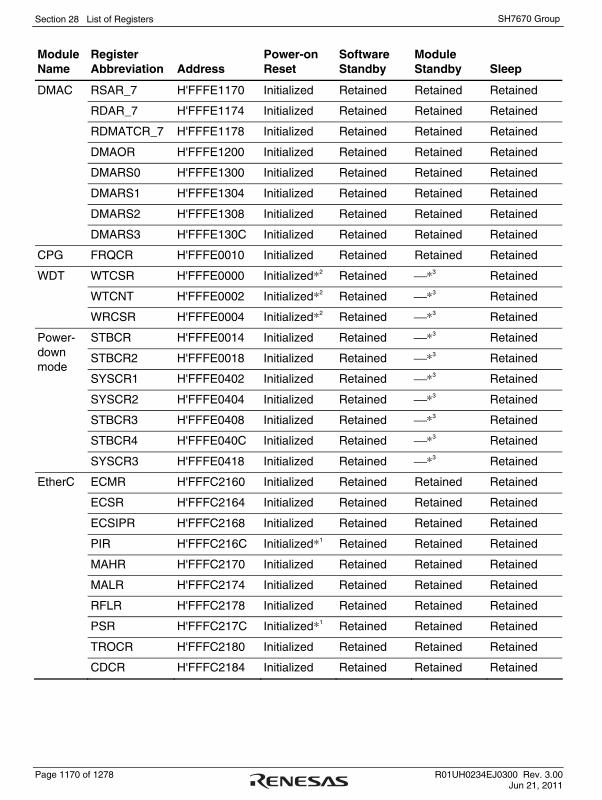
Section 28 List of Registers
Page 1170 of 1278 R01UH0234EJ0300 Rev. 3.00 Jun 21, 2011
SH7670 Group
Module Name
Register Abbreviation Address
Power-on Reset
Software Standby
Module Standby Sleep
DMAC RSAR_7 H'FFFE1170 Initialized Retained Retained Retained
RDAR_7 H'FFFE1174 Initialized Retained Retained Retained
RDMATCR_7 H'FFFE1178 Initialized Retained Retained Retained
DMAOR H'FFFE1200 Initialized Retained Retained Retained
DMARS0 H'FFFE1300 Initialized Retained Retained Retained
DMARS1 H'FFFE1304 Initialized Retained Retained Retained
DMARS2 H'FFFE1308 Initialized Retained Retained Retained
DMARS3 H'FFFE130C Initialized Retained Retained Retained
CPG FRQCR H'FFFE0010 Initialized Retained Retained Retained
WDT WTCSR H'FFFE0000 Initialized*2 Retained ⎯*3 Retained
WTCNT H'FFFE0002 Initialized*2 Retained ⎯*3 Retained
WRCSR H'FFFE0004 Initialized*2 Retained ⎯*3 Retained
STBCR H'FFFE0014 Initialized Retained ⎯*3 Retained
STBCR2 H'FFFE0018 Initialized Retained ⎯*3 Retained
Power-down mode
SYSCR1 H'FFFE0402 Initialized Retained ⎯*3 Retained
SYSCR2 H'FFFE0404 Initialized Retained ⎯*3 Retained
STBCR3 H'FFFE0408 Initialized Retained ⎯*3 Retained
STBCR4 H'FFFE040C Initialized Retained ⎯*3 Retained
SYSCR3 H'FFFE0418 Initialized Retained ⎯*3 Retained
EtherC ECMR H'FFFC2160 Initialized Retained Retained Retained
ECSR H'FFFC2164 Initialized Retained Retained Retained
ECSIPR H'FFFC2168 Initialized Retained Retained Retained
PIR H'FFFC216C Initialized*1 Retained Retained Retained
MAHR H'FFFC2170 Initialized Retained Retained Retained
MALR H'FFFC2174 Initialized Retained Retained Retained
RFLR H'FFFC2178 Initialized Retained Retained Retained
PSR H'FFFC217C Initialized*1 Retained Retained Retained
TROCR H'FFFC2180 Initialized Retained Retained Retained
CDCR H'FFFC2184 Initialized Retained Retained Retained
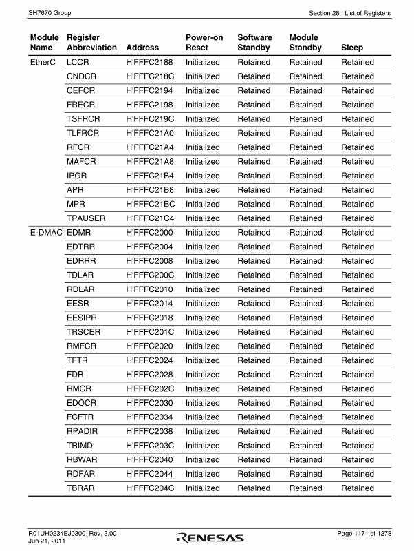
Section 28 List of Registers
R01UH0234EJ0300 Rev. 3.00 Page 1171 of 1278 Jun 21, 2011
SH7670 Group
Module Name
Register Abbreviation Address
Power-on Reset
Software Standby
Module Standby Sleep
EtherC LCCR H'FFFC2188 Initialized Retained Retained Retained
CNDCR H'FFFC218C Initialized Retained Retained Retained
CEFCR H'FFFC2194 Initialized Retained Retained Retained
FRECR H'FFFC2198 Initialized Retained Retained Retained
TSFRCR H'FFFC219C Initialized Retained Retained Retained
TLFRCR H'FFFC21A0 Initialized Retained Retained Retained
RFCR H'FFFC21A4 Initialized Retained Retained Retained
MAFCR H'FFFC21A8 Initialized Retained Retained Retained
IPGR H'FFFC21B4 Initialized Retained Retained Retained
APR H'FFFC21B8 Initialized Retained Retained Retained
MPR H'FFFC21BC Initialized Retained Retained Retained
TPAUSER H'FFFC21C4 Initialized Retained Retained Retained
E-DMAC EDMR H'FFFC2000 Initialized Retained Retained Retained
EDTRR H'FFFC2004 Initialized Retained Retained Retained
EDRRR H'FFFC2008 Initialized Retained Retained Retained
TDLAR H'FFFC200C Initialized Retained Retained Retained
RDLAR H'FFFC2010 Initialized Retained Retained Retained
EESR H'FFFC2014 Initialized Retained Retained Retained
EESIPR H'FFFC2018 Initialized Retained Retained Retained
TRSCER H'FFFC201C Initialized Retained Retained Retained
RMFCR H'FFFC2020 Initialized Retained Retained Retained
TFTR H'FFFC2024 Initialized Retained Retained Retained
FDR H'FFFC2028 Initialized Retained Retained Retained
RMCR H'FFFC202C Initialized Retained Retained Retained
EDOCR H'FFFC2030 Initialized Retained Retained Retained
FCFTR H'FFFC2034 Initialized Retained Retained Retained
RPADIR H'FFFC2038 Initialized Retained Retained Retained
TRIMD H'FFFC203C Initialized Retained Retained Retained
RBWAR H'FFFC2040 Initialized Retained Retained Retained
RDFAR H'FFFC2044 Initialized Retained Retained Retained
TBRAR H'FFFC204C Initialized Retained Retained Retained

Section 28 List of Registers
Page 1172 of 1278 R01UH0234EJ0300 Rev. 3.00 Jun 21, 2011
SH7670 Group
Module Name
Register Abbreviation Address
Power-on Reset
Software Standby
Module Standby Sleep
E-DMAC TDFAR H'FFFC2050 Initialized Retained Retained Retained
CSMR H'FFFC20E4 Initialized Retained Retained Retained
CSSBM H'FFFC20E8 Initialized Retained Retained Retained
CSSMR H'FFFC20EC Initialized Retained Retained Retained
A-DMAC C0C H'FFFC2440 Initialized Retained Retained Retained
C0M H'FFFC2444 Initialized Retained Retained Retained
C0I H'FFFC2448 Initialized Retained Retained Retained
C0DSA H'FFFC247C Initialized Retained Retained Retained
C0DCA H'FFFC2480 Initialized Retained Retained Retained
C0D0 H'FFFC2484 Initialized Retained Retained Retained
C0D1 H'FFFC2488 Initialized Retained Retained Retained
C0D2 H'FFFC248C Initialized Retained Retained Retained
C0D3 H'FFFC2490 Initialized Retained Retained Retained
C0D4 H'FFFC2494 Initialized Retained Retained Retained
C1C H'FFFC24B0 Initialized Retained Retained Retained
C1M H'FFFC24B4 Initialized Retained Retained Retained
C1I H'FFFC24B8 Initialized Retained Retained Retained
C1DSA H'FFFC24EC Initialized Retained Retained Retained
C1DCA H'FFFC24F0 Initialized Retained Retained Retained
C1D0 H'FFFC24F4 Initialized Retained Retained Retained
C1D1 H'FFFC24F8 Initialized Retained Retained Retained
C1D2 H'FFFC24FC Initialized Retained Retained Retained
C1D3 H'FFFC2500 Initialized Retained Retained Retained
C1D4 H'FFFC2504 Initialized Retained Retained Retained
FECC H'FFFC2590 Initialized Retained Retained Retained
FECI H'FFFC2594 Initialized Retained Retained Retained
FECDSA H'FFFC2598 Initialized Retained Retained Retained
FECDCA H'FFFC259C Initialized Retained Retained Retained
FECD00 H'FFFC25A0 Initialized Retained Retained Retained
FECD01D0A H'FFFC25A4 Initialized Retained Retained Retained
FECD02S0A H'FFFC25A8 Initialized Retained Retained Retained

Section 28 List of Registers
R01UH0234EJ0300 Rev. 3.00 Page 1173 of 1278 Jun 21, 2011
SH7670 Group
Module Name
Register Abbreviation Address
Power-on Reset
Software Standby
Module Standby Sleep
A-DMAC FECD03S1A H'FFFC25AC Initialized Retained Retained Retained
STIF0 STMDR_0 H'FFFFD000 Initialized Retained Retained Retained
STCTLR_0 H'FFFFD004 Initialized Retained Retained Retained
STCNTCR_0 H'FFFFD008 Initialized Retained Retained Retained
STCNTVR_0 H'FFFFD00C Initialized Retained Retained Retained
STSTR_0 H'FFFFD010 Initialized Retained Retained Retained
STIER_0 H'FFFFD014 Initialized Retained Retained Retained
STSIZER_0 H'FFFFD018 Initialized Retained Retained Retained
STPWMMR_0 H'FFFFD020 Initialized Retained Retained Retained
STPWMCR_0 H'FFFFD024 Initialized Retained Retained Retained
STPWMR_0 H'FFFFD028 Initialized Retained Retained Retained
STPCR0R_0 H'FFFFD02C Initialized Retained Retained Retained
STPCR1R_0 H'FFFFD030 Initialized Retained Retained Retained
STSTC0R_0 H'FFFFD034 Initialized Retained Retained Retained
STSTC1R_0 H'FFFFD038 Initialized Retained Retained Retained
STLKCR_0 H'FFFFD03C Initialized Retained Retained Retained
STDBGR_0 H'FFFFD060 Initialized Retained Retained Retained
STIF1 STMDR_1 H'FFFFD800 Initialized Retained Retained Retained
STCTLR_1 H'FFFFD804 Initialized Retained Retained Retained
STCNTCR_1 H'FFFFD808 Initialized Retained Retained Retained
STCNTVR_1 H'FFFFD80C Initialized Retained Retained Retained
STSTR_1 H'FFFFD810 Initialized Retained Retained Retained
STIER_1 H'FFFFD814 Initialized Retained Retained Retained
STSIZER_1 H'FFFFD818 Initialized Retained Retained Retained
STPWMMR_1 H'FFFFD820 Initialized Retained Retained Retained
STPWMCR_1 H'FFFFD824 Initialized Retained Retained Retained
STPWMR_1 H'FFFFD828 Initialized Retained Retained Retained
STPCR0R_1 H'FFFFD82C Initialized Retained Retained Retained
STPCR1R_1 H'FFFFD830 Initialized Retained Retained Retained
STSTC0R_1 H'FFFFD834 Initialized Retained Retained Retained
STSTC1R_1 H'FFFFD838 Initialized Retained Retained Retained

Section 28 List of Registers
Page 1174 of 1278 R01UH0234EJ0300 Rev. 3.00 Jun 21, 2011
SH7670 Group
Module Name
Register Abbreviation Address
Power-on Reset
Software Standby
Module Standby Sleep
STIF1 STLKCR_1 H'FFFFD83C Initialized Retained Retained Retained
STDBGR_1 H'FFFFD860 Initialized Retained Retained Retained
SSI SCSR_0 H'FFFF0000 Initialized Retained Retained Retained
SCSR_1 H'FFFF0800 Initialized Retained Retained Retained
SSICR_0 H'FFFFC000 Initialized Retained Retained Retained
SSISR_0 H'FFFFC004 Initialized Retained Retained Retained
SSITDR_0 H'FFFFC008 Initialized Retained Retained Retained
SSIRDR_0 H'FFFFC00C Initialized Retained Retained Retained
SSICR_1 H'FFFFC800 Initialized Retained Retained Retained
SSISR_1 H'FFFFC804 Initialized Retained Retained Retained
SSITDR_1 H'FFFFC808 Initialized Retained Retained Retained
SSIRDR_1 H'FFFFC80C Initialized Retained Retained Retained
USB D0FWAIT H'FFFC1C0C Initialized Retained Retained Retained
D1FWAIT H'FFFC1C0E Initialized Retained Retained Retained
D0FIFO H'FFFC1C14 Initialized Retained Retained Retained
D1FIFO H'FFFC1C18 Initialized Retained Retained Retained
SYSCFG H'FFFFF800 Initialized Retained Retained Retained
BUSWAIT H'FFFFF802 Initialized Retained Retained Retained
SYSSTS H'FFFFF804 Initialized Retained Retained Retained
DVSTCTR H'FFFFF808 Initialized Retained Retained Retained
TESTMODE H'FFFFF80C Initialized Retained Retained Retained
D0FBCFG H'FFFFF810 Initialized Retained Retained Retained
D1FBCFG H'FFFFF812 Initialized Retained Retained Retained
CFIFO H'FFFFF814 Initialized Retained Retained Retained
CFIFOSEL H'FFFFF820 Initialized Retained Retained Retained
CFIFOCTR H'FFFFF822 Initialized Retained Retained Retained
D0FIFOSEL H'FFFFF828 Initialized Retained Retained Retained
D0FIFOCTR H'FFFFF82A Initialized Retained Retained Retained
D1FIFOSEL H'FFFFF82C Initialized Retained Retained Retained
D1FIFOCTR H'FFFFF82E Initialized Retained Retained Retained
INTENB0 H'FFFFF830 Initialized Retained Retained Retained
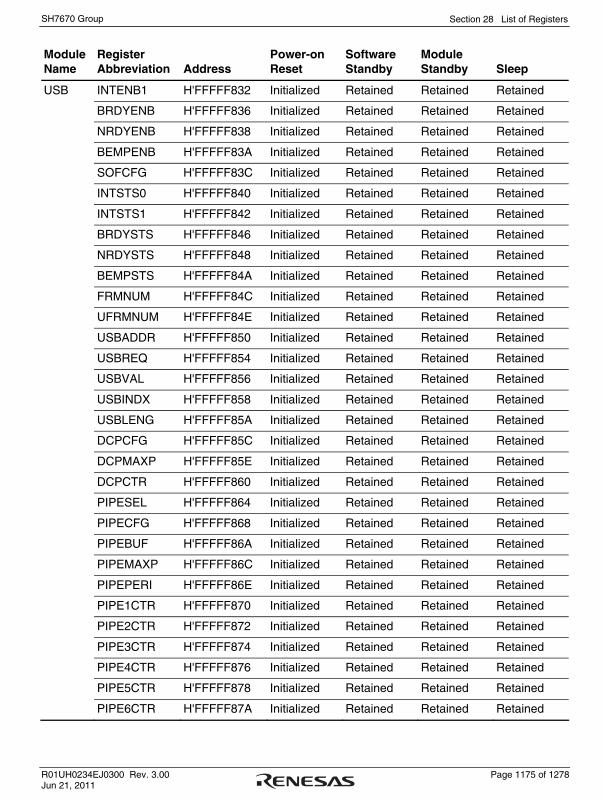
Section 28 List of Registers
R01UH0234EJ0300 Rev. 3.00 Page 1175 of 1278 Jun 21, 2011
SH7670 Group
Module Name
Register Abbreviation Address
Power-on Reset
Software Standby
Module Standby Sleep
USB INTENB1 H'FFFFF832 Initialized Retained Retained Retained
BRDYENB H'FFFFF836 Initialized Retained Retained Retained
NRDYENB H'FFFFF838 Initialized Retained Retained Retained
BEMPENB H'FFFFF83A Initialized Retained Retained Retained
SOFCFG H'FFFFF83C Initialized Retained Retained Retained
INTSTS0 H'FFFFF840 Initialized Retained Retained Retained
INTSTS1 H'FFFFF842 Initialized Retained Retained Retained
BRDYSTS H'FFFFF846 Initialized Retained Retained Retained
NRDYSTS H'FFFFF848 Initialized Retained Retained Retained
BEMPSTS H'FFFFF84A Initialized Retained Retained Retained
FRMNUM H'FFFFF84C Initialized Retained Retained Retained
UFRMNUM H'FFFFF84E Initialized Retained Retained Retained
USBADDR H'FFFFF850 Initialized Retained Retained Retained
USBREQ H'FFFFF854 Initialized Retained Retained Retained
USBVAL H'FFFFF856 Initialized Retained Retained Retained
USBINDX H'FFFFF858 Initialized Retained Retained Retained
USBLENG H'FFFFF85A Initialized Retained Retained Retained
DCPCFG H'FFFFF85C Initialized Retained Retained Retained
DCPMAXP H'FFFFF85E Initialized Retained Retained Retained
DCPCTR H'FFFFF860 Initialized Retained Retained Retained
PIPESEL H'FFFFF864 Initialized Retained Retained Retained
PIPECFG H'FFFFF868 Initialized Retained Retained Retained
PIPEBUF H'FFFFF86A Initialized Retained Retained Retained
PIPEMAXP H'FFFFF86C Initialized Retained Retained Retained
PIPEPERI H'FFFFF86E Initialized Retained Retained Retained
PIPE1CTR H'FFFFF870 Initialized Retained Retained Retained
PIPE2CTR H'FFFFF872 Initialized Retained Retained Retained
PIPE3CTR H'FFFFF874 Initialized Retained Retained Retained
PIPE4CTR H'FFFFF876 Initialized Retained Retained Retained
PIPE5CTR H'FFFFF878 Initialized Retained Retained Retained
PIPE6CTR H'FFFFF87A Initialized Retained Retained Retained

Section 28 List of Registers
Page 1176 of 1278 R01UH0234EJ0300 Rev. 3.00 Jun 21, 2011
SH7670 Group
Module Name
Register Abbreviation Address
Power-on Reset
Software Standby
Module Standby Sleep
USB PIPE7CTR H'FFFFF87C Initialized Retained Retained Retained
PIPE8CTR H'FFFFF87E Initialized Retained Retained Retained
PIPE9CTR H'FFFFF880 Initialized Retained Retained Retained
PIPE1TRE H'FFFFF890 Initialized Retained Retained Retained
PIPE1TRN H'FFFFF892 Initialized Retained Retained Retained
PIPE2TRE H'FFFFF894 Initialized Retained Retained Retained
PIPE2TRN H'FFFFF896 Initialized Retained Retained Retained
PIPE3TRE H'FFFFF898 Initialized Retained Retained Retained
PIPE3TRN H'FFFFF89A Initialized Retained Retained Retained
PIPE4TRE H'FFFFF89C Initialized Retained Retained Retained
PIPE4TRN H'FFFFF89E Initialized Retained Retained Retained
PIPE5TRE H'FFFFF8A0 Initialized Retained Retained Retained
PIPE5TRN H'FFFFF8A2 Initialized Retained Retained Retained
DEVADD0 H'FFFFF8D0 Initialized Retained Retained Retained
DEVADD1 H'FFFFF8D2 Initialized Retained Retained Retained
DEVADD2 H'FFFFF8D4 Initialized Retained Retained Retained
DEVADD3 H'FFFFF8D6 Initialized Retained Retained Retained
DEVADD4 H'FFFFF8D8 Initialized Retained Retained Retained
DEVADD5 H'FFFFF8DA Initialized Retained Retained Retained
DEVADD6 H'FFFFF8DC Initialized Retained Retained Retained
DEVADD7 H'FFFFF8DE Initialized Retained Retained Retained
DEVADD8 H'FFFFF8E0 Initialized Retained Retained Retained
DEVADD9 H'FFFFF8E2 Initialized Retained Retained Retained
DEVADDA H'FFFFF8E4 Initialized Retained Retained Retained
IIC3 ICCR1_0 H'FFFEE000 Initialized Retained Retained Retained
ICCR2_0 H'FFFEE001 Initialized Retained Retained Retained
ICMR_0 H'FFFEE002 Initialized Retained Retained Retained
ICIER_0 H'FFFEE003 Initialized Retained Retained Retained
ICSR_0 H'FFFEE004 Initialized Retained Retained Retained
SAR_0 H'FFFEE005 Initialized Retained Retained Retained
ICDRT_0 H'FFFEE006 Initialized Retained Retained Retained

Section 28 List of Registers
R01UH0234EJ0300 Rev. 3.00 Page 1177 of 1278 Jun 21, 2011
SH7670 Group
Module Name
Register Abbreviation Address
Power-on Reset
Software Standby
Module Standby Sleep
IIC3 ICDRR_0 H'FFFEE007 Initialized Retained Retained Retained
NF2CYC_0 H'FFFEE008 Initialized Retained Retained Retained
HIF HIFIDX H'FFFFE000 Initialized Retained Retained Retained
HIFGSR H'FFFFE004 Initialized Retained Retained Retained
HIFSCR H'FFFFE008 Initialized*1 Retained Retained Retained
HIFMCR H'FFFFE00C Initialized Retained Retained Retained
HIFIICR H'FFFFE010 Initialized Retained Retained Retained
HIFEICR H'FFFFE014 Initialized Retained Retained Retained
HIFADR H'FFFFE018 Initialized Retained Retained Retained
HIFDATA H'FFFFE01C Initialized Retained Retained Retained
HIFDTR H'FFFFE020 Initialized Retained Retained Retained
HIFBICR H'FFFFE024 Initialized Retained Retained Retained
HIFBCR H'FFFFE040 Initialized*1 Retained Retained Retained
CMT CMSTR H'FFFEC000 Initialized Initialized Retained Retained
CMCSR_0 H'FFFEC002 Initialized Initialized Retained Retained
CMCNT_0 H'FFFEC004 Initialized Initialized Retained Retained
CMCOR_0 H'FFFEC006 Initialized Initialized Retained Retained
CMCSR_1 H'FFFEC008 Initialized Initialized Retained Retained
CMCNT_1 H'FFFEC00A Initialized Initialized Retained Retained
CMCOR_1 H'FFFEC00C Initialized Initialized Retained Retained
SCIF0 SCSMR_0 H'FFFE8000 Initialized Retained Retained Retained
SCBRR_0 H'FFFE8004 Initialized Retained Retained Retained
SCSCR_0 H'FFFE8008 Initialized Retained Retained Retained
SCFTDR_0 H'FFFE800C Undefined Retained Retained Retained
SCFSR_0 H'FFFE8010 Initialized Retained Retained Retained
SCFRDR_0 H'FFFE8014 Undefined Retained Retained Retained
SCFCR_0 H'FFFE8018 Initialized Retained Retained Retained
SCFDR_0 H'FFFE801C Initialized Retained Retained Retained
SCSPTR_0 H'FFFE8020 Initialized*1 Retained Retained Retained
SCLSR_0 H'FFFE8024 Initialized Retained Retained Retained
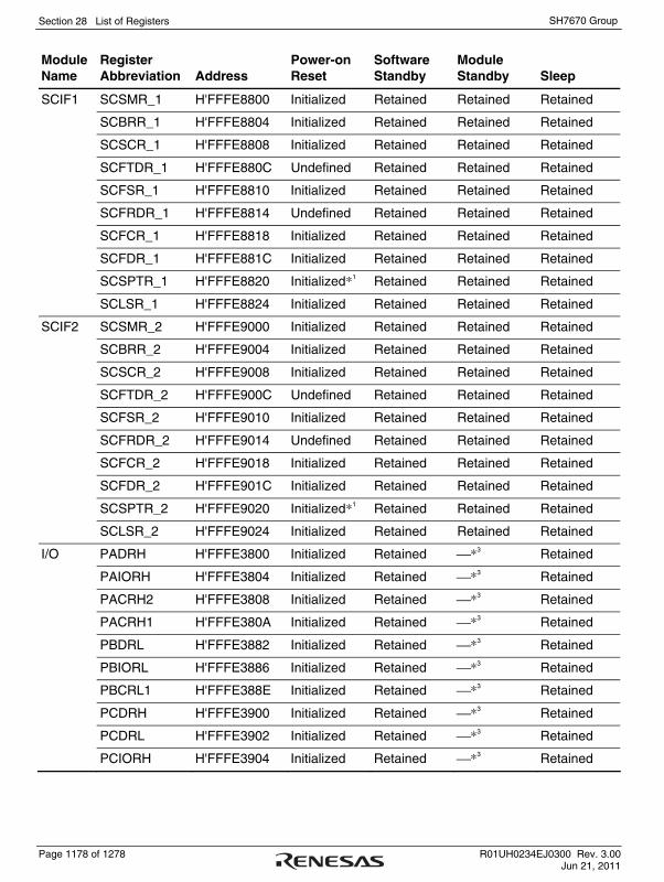
Section 28 List of Registers
Page 1178 of 1278 R01UH0234EJ0300 Rev. 3.00 Jun 21, 2011
SH7670 Group
Module Name
Register Abbreviation Address
Power-on Reset
Software Standby
Module Standby Sleep
SCIF1 SCSMR_1 H'FFFE8800 Initialized Retained Retained Retained
SCBRR_1 H'FFFE8804 Initialized Retained Retained Retained
SCSCR_1 H'FFFE8808 Initialized Retained Retained Retained
SCFTDR_1 H'FFFE880C Undefined Retained Retained Retained
SCFSR_1 H'FFFE8810 Initialized Retained Retained Retained
SCFRDR_1 H'FFFE8814 Undefined Retained Retained Retained
SCFCR_1 H'FFFE8818 Initialized Retained Retained Retained
SCFDR_1 H'FFFE881C Initialized Retained Retained Retained
SCSPTR_1 H'FFFE8820 Initialized*1 Retained Retained Retained
SCLSR_1 H'FFFE8824 Initialized Retained Retained Retained
SCIF2 SCSMR_2 H'FFFE9000 Initialized Retained Retained Retained
SCBRR_2 H'FFFE9004 Initialized Retained Retained Retained
SCSCR_2 H'FFFE9008 Initialized Retained Retained Retained
SCFTDR_2 H'FFFE900C Undefined Retained Retained Retained
SCFSR_2 H'FFFE9010 Initialized Retained Retained Retained
SCFRDR_2 H'FFFE9014 Undefined Retained Retained Retained
SCFCR_2 H'FFFE9018 Initialized Retained Retained Retained
SCFDR_2 H'FFFE901C Initialized Retained Retained Retained
SCSPTR_2 H'FFFE9020 Initialized*1 Retained Retained Retained
SCLSR_2 H'FFFE9024 Initialized Retained Retained Retained
I/O PADRH H'FFFE3800 Initialized Retained ⎯*3 Retained
PAIORH H'FFFE3804 Initialized Retained ⎯*3 Retained
PACRH2 H'FFFE3808 Initialized Retained ⎯*3 Retained
PACRH1 H'FFFE380A Initialized Retained ⎯*3 Retained
PBDRL H'FFFE3882 Initialized Retained ⎯*3 Retained
PBIORL H'FFFE3886 Initialized Retained ⎯*3 Retained
PBCRL1 H'FFFE388E Initialized Retained ⎯*3 Retained
PCDRH H'FFFE3900 Initialized Retained ⎯*3 Retained
PCDRL H'FFFE3902 Initialized Retained ⎯*3 Retained
PCIORH H'FFFE3904 Initialized Retained ⎯*3 Retained

Section 28 List of Registers
R01UH0234EJ0300 Rev. 3.00 Page 1179 of 1278 Jun 21, 2011
SH7670 Group
Module Name
Register Abbreviation Address
Power-on Reset
Software Standby
Module Standby Sleep
I/O PCIORL H'FFFE3906 Initialized Retained ⎯*3 Retained
PCCRH1 H'FFFE390A Initialized Retained ⎯*3 Retained
PCCRL2 H'FFFE390C Initialized Retained ⎯*3 Retained
PCCRL1 H'FFFE390E Initialized Retained ⎯*3 Retained
PDDRL H'FFFE3982 Initialized Retained ⎯*3 Retained
PDIORL H'FFFE3986 Initialized Retained ⎯*3 Retained
PDCRL1 H'FFFE398E Initialized Retained ⎯*3 Retained
PEDRL H'FFFE3A02 Initialized Retained ⎯*3 Retained
PEIORL H'FFFE3A06 Initialized Retained ⎯*3 Retained
PECRL2 H'FFFE3A0C Initialized Retained ⎯*3 Retained
PECRL1 H'FFFE3A0E Initialized Retained ⎯*3 Retained
PFDRL H'FFFE3A82 Initialized Retained ⎯*3 Retained
PFIORL H'FFFE3A86 Initialized Retained ⎯*3 Retained
PFCRL2 H'FFFE3A8C Initialized Retained ⎯*3 Retained
PFCRL1 H'FFFE3A8E Initialized Retained ⎯*3 Retained
PGDRH H'FFFE3B00 Initialized Retained ⎯*3 Retained
PGDRL H'FFFE3B02 Initialized Retained ⎯*3 Retained
PGIORH H'FFFE3B04 Initialized Retained ⎯*3 Retained
PGIORL H'FFFE3B06 Initialized Retained ⎯*3 Retained
PGCRH2 H'FFFE3B0A Initialized Retained ⎯*3 Retained
PGCRL2 H'FFFE3B0C Initialized Retained ⎯*3 Retained
PGCRL1 H'FFFE3B0E Initialized Retained ⎯*3 Retained
UBC BAR_0 H'FFFC0400 Initialized Retained Retained Retained
BAMR_0 H'FFFC0404 Initialized Retained Retained Retained
BDR_0 H'FFFC0408 Initialized Retained Retained Retained
BDMR_0 H'FFFC040C Initialized Retained Retained Retained
BAR_1 H'FFFC0410 Initialized Retained Retained Retained
BAMR_1 H'FFFC0414 Initialized Retained Retained Retained
BDR_1 H'FFFC0418 Initialized Retained Retained Retained
BDMR_1 H'FFFC041C Initialized Retained Retained Retained

Section 28 List of Registers
Page 1180 of 1278 R01UH0234EJ0300 Rev. 3.00 Jun 21, 2011
SH7670 Group
Module Name
Register Abbreviation Address
Power-on Reset
Software Standby
Module Standby Sleep
UBC BBR_0 H'FFFC04A0 Initialized Retained Retained Retained
BBR_1 H'FFFC04B0 Initialized Retained Retained Retained
BRCR H'FFFC04C0 Initialized Retained Retained Retained
H-UDI SDIR H'FFFE2000 Retained Retained Retained Retained
Notes: 1. There are bits that will not be initialized. 2. No initialization occurs if a WDT-based power-on reset is used.
3. This module provides no module standby function.
4. This is not a reset based on the power-on reset pin, but it is initialization performed by applying the PHY power supply.
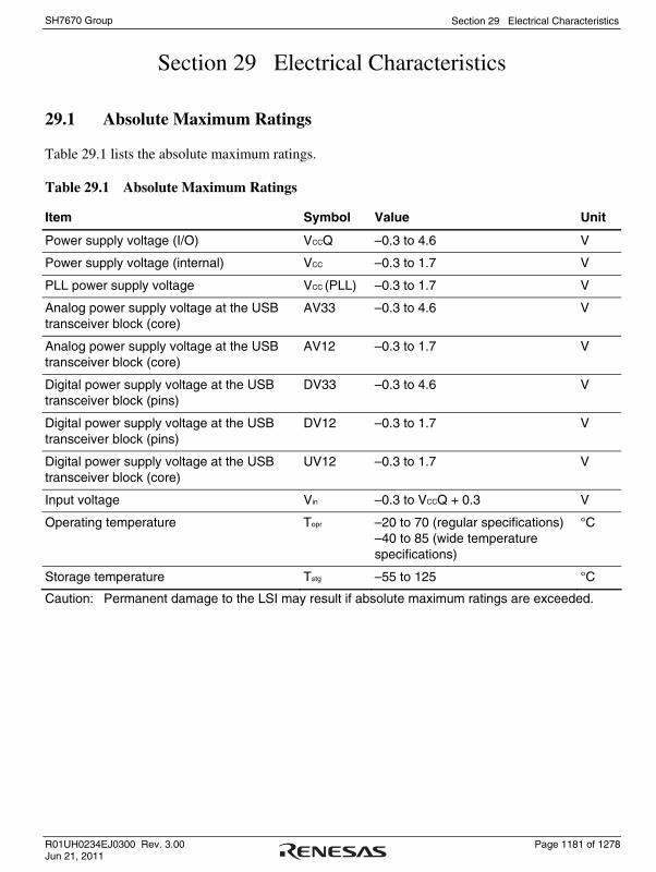
Section 29 Electrical Characteristics
R01UH0234EJ0300 Rev. 3.00 Page 1181 of 1278 Jun 21, 2011
SH7670 Group
Section 29 Electrical Characteristics
29.1 Absolute Maximum Ratings
Table 29.1 lists the absolute maximum ratings.
Table 29.1 Absolute Maximum Ratings
Item Symbol Value Unit
Power supply voltage (I/O) VCCQ –0.3 to 4.6 V
Power supply voltage (internal) VCC –0.3 to 1.7 V
PLL power supply voltage VCC (PLL) –0.3 to 1.7 V
Analog power supply voltage at the USB transceiver block (core)
AV33 –0.3 to 4.6 V
Analog power supply voltage at the USB transceiver block (core)
AV12 –0.3 to 1.7 V
Digital power supply voltage at the USB transceiver block (pins)
DV33 –0.3 to 4.6 V
Digital power supply voltage at the USB transceiver block (pins)
DV12 –0.3 to 1.7 V
Digital power supply voltage at the USB transceiver block (core)
UV12 –0.3 to 1.7 V
Input voltage Vin –0.3 to VCCQ + 0.3 V
Operating temperature Topr –20 to 70 (regular specifications) –40 to 85 (wide temperature specifications)
°C
Storage temperature Tstg –55 to 125 °C
Caution: Permanent damage to the LSI may result if absolute maximum ratings are exceeded.
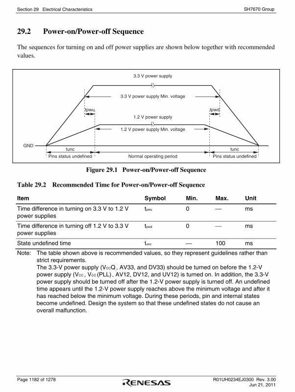
Section 29 Electrical Characteristics
Page 1182 of 1278 R01UH0234EJ0300 Rev. 3.00 Jun 21, 2011
SH7670 Group
29.2 Power-on/Power-off Sequence
The sequences for turning on and off power supplies are shown below together with recommended values.
3.3 V power supply
3.3 V power supply Min. voltage
1.2 V power supply
1.2 V power supply Min. voltage
tunc
tpwu tpwd
GND
Pins status undefined
tunc
Pins status undefinedNormal operating period
Figure 29.1 Power-on/Power-off Sequence
Table 29.2 Recommended Time for Power-on/Power-off Sequence
Item Symbol Min. Max. Unit
Time difference in turning on 3.3 V to 1.2 V power supplies
tpwu 0 ⎯ ms
Time difference in turning off 1.2 V to 3.3 V power supplies
tpwd 0 ⎯ ms
State undefined time tunc ⎯ 100 ms
Note: The table shown above is recommended values, so they represent guidelines rather than strict requirements. The 3.3-V power supply (VCCQ,, AV33, and DV33) should be turned on before the 1.2-V power supply (VCC , VCC (PLL) , AV12, DV12, and UV12) is turned on. In addition, the 3.3-V power supply should be turned off after the 1.2-V power supply is turned off. An undefined time appears until the 1.2-V power supply reaches above the minimum voltage and after it has reached below the minimum voltage. During these periods, pin and internal states become undefined. Design the system so that these undefined states do not cause an overall malfunction.

Section 29 Electrical Characteristics
R01UH0234EJ0300 Rev. 3.00 Page 1183 of 1278 Jun 21, 2011
SH7670 Group
29.3 DC Characteristics
Table 29.3 DC Characteristics (1) [Common Items]
Conditions: VCC = VCC (PLL) = DV12 = UV12 = 1.1 to 1.3 V, VCCQ = DV33 = 3.1 to 3.5 V,
AV12 = 1.1 to 1.3 V, AV33 = 3.1 to 3.5 V, VSS = VSS (PLL) = DG12 = UG12 = VSSQ = DG33 = AG12 = AG33 = 0 V,
Ta = –20 to 70°C (regular specifications), –40 to 85°C (wide temperature specifications)
Item Symbol Min. Typ. Max. Unit Test Conditions
VCCQ 3.1 3.3 3.5 V Power supply voltage
VCC 1.1 1.2 1.3 V
PLL power supply voltage VCC (PLL) 1.1 1.2 1.3 V
AV33
DV33 3.1 3.3 3.5 V USB power supply voltage
AV12 DV12 UV12
1.1 1.2 1.3 V
50*3 70*3 VCCQ ICC0 ⎯
33*4 50*4
DV33 ICC1*2 ⎯ 44 65
230*3 460*3 VCC
VCC (PLL)
ICC2 ⎯
166*4 400*4
DV12 UV12
ICC3*2 ⎯ 32 55
AV33 ICC4*2 ⎯ 4 5
Normal operation
AV12 ICC5*2 ⎯ 14 16
mA Values measured at maximum power supply voltages. Regular specifications: Iφ = 200 MHz Bφ = 100 MHz Pφ = 50 MHz
Wide temperature specifications: Iφ = 133.3 MHz Bφ = 66.6 MHz Pφ = 33.3 MHz
50*3 70*3 VCCQ Isleep0 ⎯
33*4 50*4
DV33 Isleep1*2 ⎯ 44 65
170*3 400*3 VCC
VCC (PLL)
Isleep2 ⎯
127*4 360*4
DV12 UV12
Isleep3*2 ⎯ 32 55
AV33 Isleep4*2 ⎯ 4 5
Supply current*1
Sleep mode
AV12 Isleep5*2 ⎯ 14 16
mA Values measured at maximum power supply voltages. Regular specifications: Iφ = 200 MHz Bφ = 100 MHz Pφ = 50 MHz
Wide temperature specifications: Iφ = 133.3 MHz Bφ = 66.6 MHz Pφ = 33.3 MHz

Section 29 Electrical Characteristics
Page 1184 of 1278 R01UH0234EJ0300 Rev. 3.00 Jun 21, 2011
SH7670 Group
Item Symbol Min. Typ. Max. Unit Test Conditions
VCCQ DV33
Isstby00 ⎯ 38 45 μA
VCC VCC (PLL) DV12 UV12
Isstby01 ⎯ 250 280 mA
AV33 Isstby02 ⎯ 20 40
AV12 Isstby03 ⎯ 2 5
μA
Ta > 50°C
Values measured at maximum power supply voltages
VCCQ DV33
Isstby10 ⎯ 35 42 μA
VCC VCC (PLL) DV12 UV12
Isstby11 ⎯ 40 80 mA
AV33 Isstby12 ⎯ 20 40 μA
Supply current*5
Software standby mode
AV12 Isstby13 ⎯ 2 5
Ta ≤ 50°C
Values measured at maximum power supply voltages
All input pins (except PB7 to PB0)
⎯ ⎯ 1.0 μA Input leakage current PB01,PB00
|Iin |
⎯ ⎯ 10 μA
Vin = 0.5 to VCCQ – 0.5 V
Three-state leakage current
All input/output pins, output pins
|ISTI | ⎯ ⎯ 1.0 μA Vin = 0.5 to VCCQ – 0.5 V
Pin capacitance
All pins Cin ⎯ ⎯ 15 pF
Notes: 1. Supply current values are the values measured when all of the output pins and pins with the pull-up function are unloaded.
2. In USB operations.
3. Regular specifications 4. Wide temperature specifications
5. Supply current values are the values measured when all the output pins are unloaded.

Section 29 Electrical Characteristics
R01UH0234EJ0300 Rev. 3.00 Page 1185 of 1278 Jun 21, 2011
SH7670 Group
Table 29.3 DC Characteristics (2) [Excluding the Pins Related to I2C and USB]
Conditions: VCC = VCC (PLL) = DV12 = UV12 = 1.1 to 1.3 V, VCCQ = DV33 = 3.1 to 3.5 V, AV12 = 1.1 to 1.3 V, AV33 = 3.1 to 3.5 V, VSS = VSS (PLL) = DG12 = UG12 = VSSQ = DG33 = AG12 = AG33 = 0 V, Ta = –20 to 70°C (regular specifications), –40 to 85°C (wide temperature specifications)
Item Symbol Min. Typ. Max. Unit Test Conditions
EXTAL, CKIO, RES, TCK, TRST, ASEMD, TESTMD, MD_BW, MD_CK1, MD_CK0, NMI, ST1_CLKIN/SSISCK1, ST1_VCO_CLKIN/AUDIO_CLK, ST0_CLKIN/SSISCK0, ST0_VCO_CLKIN/AUDIO_CLK, ST1_CLKIN/SSISCK1, ST1_VCO_CLKIN/AUDIO_CLK, ST0_CLKIN/SSISCK0, ST0_VCO_CLKIN/AUDIO_CLK
VCCQ – 0.3
⎯ VCCQ + 0.3
V Input high voltage
Input pins other than above (excluding PB0 to PB00)
VIH
2.1 ⎯ VCCQ + 0.3
V
EXTAL, CKIO, RES, TCK, TRST, ASEMD, MD_BW, MD_CK1, MD_CK0, NMI
–0.3 ⎯ 0.3 V Input low voltage
Input pins other than above (excluding PB0 to PB00)
VIL
–0.3 ⎯ 0.8 V
VIH VCCQ – 0.5
⎯ VCCQ + 0.3
V Port B input characteristics
PB07, PB06, PB05/IRQ3, PB04/IRQ2, PB03/IRQ1/DREQ1, PB02/IRQ0
VIL –0.3 ⎯ 0.5 V
Output high voltage VOH 2.4 ⎯ ⎯ V IOH = –200 μA
Output low voltage VOL ⎯ ⎯ 0.4 V IOL = 1.6 mA

Section 29 Electrical Characteristics
Page 1186 of 1278 R01UH0234EJ0300 Rev. 3.00 Jun 21, 2011
SH7670 Group
Table 29.3 DC Characteristics (3) [Pins Related to I2C*]
Conditions: VCC = VCC (PLL) = DV12 = UV12 = 1.1 to 1.3 V, VCCQ = DV33 = 3.1 to 3.5 V, AV12 = 1.1 to 1.3 V, AV33 = 3.1 to 3.5 V, VSS = VSS (PLL) = DG12 = UG12 = VSSQ = DG33 = AG12 = AG33 = 0 V, Ta = –20 to 70°C (regular specifications), –40 to 85°C (wide temperature specifications)
Item Symbol Min. Typ. Max. Unit Test Conditions
Input high voltage VIH VCC Q – 0.5 ⎯ VCC Q + 0.3 V
Input low voltage VIL –0.3 ⎯ 0.5 V
Schmitt trigger input characteristics
VIH – VIL VCC Q × 0.05
⎯ ⎯ V
Output low voltage VOL ⎯ ⎯ VCC Q × 0.2 V IOL = 3.0 mA
Note: * Referring to the PB01/IOIS16/SCL and PB00/WAIT/SDA pins (open-drain pins)
Table 29.3 DC Characteristics (4) [Pins Related to USB*]
Conditions: VCC = VCC (PLL) = DV12 = UV12 = 1.1 to 1.3 V, VCCQ = DV33 = 3.1 to 3.5 V, AV12 = 1.1 to 1.3 V, AV33 = 3.1 to 3.5 V, VSS = VSS (PLL) = DG12 = UG12 = VSSQ = DG33 = AG12 = AG33 = 0 V, Ta = –20 to 70°C (regular specifications), –40 to 85°C (wide temperature specifications)
Item Symbol Min. Typ. Max. Unit Test Conditions
Reference resistance RREF 5.6 – 1% 5.6 5.6 + 1% kΩ
Input high voltage (VBUS) VIH 4.0 ⎯ 5.5 V
Input low voltage (VBUS) VIL –0.3 ⎯ 1.0 V
Input high voltage (USB_X1) VIH VCC Q – 0.3 ⎯ VCC Q + 0.3 V
Input low voltage (USB_X1) VIL –0.3 ⎯ 0.3 V
Note: * Referring to the REFRIN, VBUS, USB_X1, and USB_X2 pins

Section 29 Electrical Characteristics
R01UH0234EJ0300 Rev. 3.00 Page 1187 of 1278 Jun 21, 2011
SH7670 Group
Table 29.3 DC Characteristics (5) [Pins Related to USB* (Low-Speed/Full-Speed/High-Speed Common Items)]
Conditions: VCC = VCC (PLL) = DV12 = UV12 = 1.1 to 1.3 V, VCCQ = DV33 = 3.1 to 3.5 V, AV12 = 1.1 to 1.3 V, AV33 = 3.1 to 3.5 V, VSS = VSS (PLL) = DG12 = UG12 = VSSQ = DG33 = AG12 = AG33 = 0 V, Ta = –20 to 70°C (regular specifications), –40 to 85°C (wide temperature specifications)
Item Symbol Min. Typ. Max. Unit Test Conditions
0.900 ⎯ 1.575 kΩ In idle mode DP pull-up resistance (when the function is selected)
Rpu
1.425 ⎯ 3.090 kΩ In transmit/receive mode
DP/DM pull-down resistance (when the host is selected)
Rpd 14.25 ⎯ 24.80 kΩ
Note: * Referring to the DP and DM pins
Table 29.3 DC Characteristics (6) [Pins Related to USB* (for Low-Speed/Full Speed)]
Conditions: VCC = VCC (PLL) = DV12 = UV12 = 1.1 to 1.3 V, VCCQ = DV33 = 3.1 to 3.5 V, AV12 = 1.1 to 1.3 V, AV33 = 3.1 to 3.5 V, VSS = VSS (PLL) = DG12 = UG12 = VSSQ = DG33 = AG12 = AG33 = 0 V, Ta = –20 to 70°C (regular specifications), –40 to 85°C (wide temperature specifications)
Item Symbol Min. Typ. Max. Unit Test Conditions
Input high voltage VIH 2.0 ⎯ ⎯ V
Input low voltage VIL ⎯ ⎯ 0.8 V
Differential input sensitivity VDI 0.2 ⎯ ⎯ V | (DP) – (DM) |
Differential common mode range
VCM 0.8 ⎯ 2.5 V
Output high voltage VOH 2.8 ⎯ ⎯ V IOH = –200 μA
Output low voltage VOH ⎯ ⎯ 0.3 V IOL = 2.0 mA
Single-ended receiver threshold voltage
VSE 0.8 ⎯ 2.0 V
Output signal crossover voltage range
VORS 1.3 ⎯ 2.0 V CL = 50 pF
Note: * Referring to the DP and DM pins

Section 29 Electrical Characteristics
Page 1188 of 1278 R01UH0234EJ0300 Rev. 3.00 Jun 21, 2011
SH7670 Group
Table 29.3 DC Characteristics (7) [Pins Related to USB* (for High Speed)]
Conditions: VCC = VCC (PLL) = DV12 = UV12 = 1.1 to 1.3 V, VCCQ = DV33 = 3.1 to 3.5 V, AV12 = 1.1 to 1.3 V, AV33 = 3.1 to 3.5 V, VSS = VSS (PLL) = DG12 = UG12 = VSSQ = DG33 = AG12 = AG33 = 0 V, Ta = –20 to 70°C (regular specifications), –40 to 85°C (wide temperature specifications)
Item Symbol Min. Typ. Max. Unit Test Conditions
Squelch-detected threshold voltage (differential voltage)
VHSSQ 100 ⎯ 150 mV
Common mode voltage range VHSCM –50 ⎯ 500 mV
Idle state VHSOI –10.0 ⎯ 10.0 mV
Output high voltage VHSOH 360 ⎯ 440 mV
Output low voltage VHSOL –10.0 ⎯ 10.0 mV
Chirp J output voltage (differential) VCHIRPJ 700 ⎯ 1100 mV
Chirp K output voltage (differential) VCHIRPK –900 ⎯ –500 mV
Note: * Referring to the DP and DM pins
Table 29.4 Permissible Output Currents
Conditions: VCC = VCC (PLL) = DV12 = UV12 = 1.1 to 1.3 V, VCCQ = DV33 = 3.1 to 3.5 V, AV12 = 1.1 to 1.3 V, AV33 = 3.1 to 3.5 V, VSS = VSS (PLL) = DG12 = UG12 = VSSQ = DG33 = AG12 = AG33 = 0 V, Ta = –20 to 70°C (regular specifications), –40 to 85°C (wide temperature specifications)
Item Symbol Min. Typ. Max. Unit
Pins related to IC2 * 10 mA Permissible output low current (per pin) Output pins other than above
IOL ⎯ ⎯
2 mA
Permissible output low current (total) Σ IOL ⎯ ⎯ 60 mA
Permissible output high current (per pin) -IOH ⎯ ⎯ 2 mA
Permissible output high current (total) Σ -IOH ⎯ ⎯ 60 mA
Note: * When use the PB01/IOIS16/SCL and PB00/WAIT/SDA pins as SCL and SDA.
Caution: To protect the LSI's reliability, do not exceed the output current values in table 29.4.

Section 29 Electrical Characteristics
R01UH0234EJ0300 Rev. 3.00 Page 1189 of 1278 Jun 21, 2011
SH7670 Group
29.4 AC Characteristics
Signals input to this LSI are basically handled as signals in synchronization with a clock. The setup and hold times for input pins must be followed.
Table 29.5 Maximum Operating Frequency
Conditions: VCC = VCC (PLL) = DV12 = UV12 = 1.1 to 1.3 V, VCCQ = DV33 = 3.1 to 3.5 V, AV12 = 1.1 to 1.3 V, AV33 = 3.1 to 3.5 V, VSS = VSS (PLL) = DG12 = UG12 = VSSQ = DG33 = AG12 = AG33 = 0 V, Ta = –20 to 70°C (regular specifications), –40 to 85°C (wide temperature specifications)
Item Symbol Min. Typ. Max. Unit Remarks
200 Regular specifications
CPU (Iφ) 60 ⎯
133.3
MHz
Wide temperature specifications
100 Regular specifications
Internal bus, external bus (Bφ)
60 ⎯
66.6
MHz
Wide temperature specifications
50 Regular specifications
Operating frequency
Peripheral module (Pφ)
f
10 ⎯
33.3
MHz
Wide temperature specifications

Section 29 Electrical Characteristics
Page 1190 of 1278 R01UH0234EJ0300 Rev. 3.00 Jun 21, 2011
SH7670 Group
29.4.1 Clock Timing
Table 29.6 Clock Timing
Conditions: VCC = VCC (PLL) = DV12 = UV12 = 1.1 to 1.3 V, VCCQ = DV33 = 3.1 to 3.5 V, AV12 = 1.1 to 1.3 V, AV33 = 3.1 to 3.5 V, VSS = VSS (PLL) = DG12 = UG12 = VSSQ = DG33 = AG12 = AG33 = 0 V, Ta = –20 to 70°C (regular specifications), –40 to 85°C (wide temperature specifications)
Item Symbol Min. Max. Unit Figure
25*2 EXTAL*1 clock input frequency fEX 15
16.6*3
MHz
40*2 EXTAL*1 clock input cycle time tEXcyc
60*3
66.6 ns
AUDIO_CLK clock input frequency fEX 10 40 MHz
AUDIO_CLK clock input cycle time tEXcyc 25 100 ns
USB_X1 clock input frequency fEX 48 48 MHz
EXTAL*1/AUDIO_CLK clock input low-level pulse width
tEXL 0.4 0.6 tEXcyc
EXTAL*1/AUDIO_CLK clock input high-level pulse width
tEXH 0.4 0.6 tEXcyc
EXTAL*1/AUDIO_CLK clock input rise time tEXr ⎯ 4 ns
EXTAL*1/SSI_CLK clock input fall time tEXf ⎯ 4 ns
29.2
100*2 CKIO clock input frequency fCK 60
66.6*3
MHz
10*2 CKIO clock input cycle time tCKIcyc
15*3
16.6 ns
CKIO clock input low-level pulse width tCKIL 0.3 0.7 tCKIcyc
CKIO clock input high-level pulse width tCKIH 0.3 0.7 tCKIcyc
CKIO clock input rise time tCKIr ⎯ 2 ns
CKIO clock input fall time tCKIf ⎯ 2 ns
29.3
100*2 CKIO clock output frequency fOP 60
66.6*3
MHz
10*2 CKIO clock output cycle time tcyc
15*3
16.6 ns
29.4

Section 29 Electrical Characteristics
R01UH0234EJ0300 Rev. 3.00 Page 1191 of 1278 Jun 21, 2011
SH7670 Group
Item Symbol Min. Max. Unit Figure
CKIO clock output low-level pulse width tCKOL 2 ⎯ ns
CKIO clock output high-level pulse width tCKOH 2 ⎯ ns
CKIO clock output rise time tCKOr ⎯ 3 ns
CKIO clock output fall time tCKOf ⎯ 3 ns
29.4
Power-on oscillation settling time tOSC1 10 ⎯ ms 29.5
Oscillation settling time on return from standby 1
tOSC2 10 ⎯ ms 29.6
Oscillation settling time on return from standby 2
tOSC3 10 ⎯ ms 29.7
Notes: 1. When the clock operating mode is 0
2. Regular specifications 3. Wide temperature specifications
tEXH
tEXf tEXr
tEXL
tEXcyc
VIH VIHVIH
1/2 VccQ 1/2 VccQVIL VIL
EXTAL,AUDIO_CLK,
USB_X1*(input)
Note: * When the clock is input on the EXTAL, AUDIO_CLK, or USB_X1 pin
Figure 29.2 EXTAL, AUDIO_CLK, and USB_X1 Clock Input Timing
tCKIH
tCKIf tCKIr
tCKIL
tCKIcyc
VIH VIHVIH
1/2 VccQ 1/2 VccQVIL VIL
CKIO(input)
Figure 29.3 CKIO Clock Input Timing

Section 29 Electrical Characteristics
Page 1192 of 1278 R01UH0234EJ0300 Rev. 3.00 Jun 21, 2011
SH7670 Group
tcyc
tCKOLtCKOH
VOH1/2 VccQ 1/2 VccQ
CKIO(output)
tCKOrtCKOf
VOH
VOL VOL
VOH
Figure 29.4 CKIO Clock Output Timing
Vcc Min.
tOSC1
Vcc
RES
CKIOInternal clock
Oscillation settling time
Note: Oscillation settling time when the internal oscillator is used
Figure 29.5 Power-On Oscillation Settling Time
CKIOInternal clock
Oscillation settling timeStandby period
tOSC2
RES
Note: Oscillation settling time when the internal oscillator is used
Figure 29.6 Oscillation Settling Time on Return from Standby (Return by Reset)
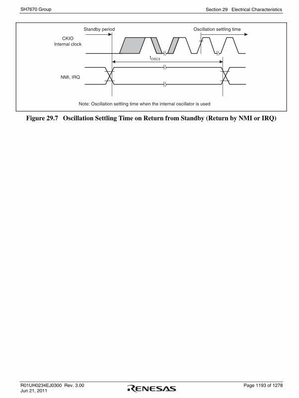
Section 29 Electrical Characteristics
R01UH0234EJ0300 Rev. 3.00 Page 1193 of 1278 Jun 21, 2011
SH7670 Group
CKIOInternal clock
Oscillation settling timeStandby period
tOSC3
NMI, IRQ
Note: Oscillation settling time when the internal oscillator is used
Figure 29.7 Oscillation Settling Time on Return from Standby (Return by NMI or IRQ)

Section 29 Electrical Characteristics
Page 1194 of 1278 R01UH0234EJ0300 Rev. 3.00 Jun 21, 2011
SH7670 Group
29.4.2 Control Signal Timing
Table 29.7 Control Signal Timing
Conditions: VCC = VCC (PLL) = DV12 = UV12 = 1.1 to 1.3 V, VCCQ = DV33 = 3.1 to 3.5 V, AV12 = 1.1 to 1.3 V, AV33 = 3.1 to 3.5 V, VSS = VSS (PLL) = DG12 = UG12 = VSSQ = DG33 = AG12 = AG33 = 0 V, Ta = –20 to 70°C (regular specifications), –40 to 85°C (wide temperature specifications)
Item Symbol Min. Max. Unit Figure
RES pulse width tRESW 20*1 ⎯ tcyc*3 29.8
NMI pulse width tNMIW 20*2 ⎯ tcyc*3
IRQ pulse width tIRQW 20*2 ⎯ tcyc*3
29.9
Notes: 1. In standby mode or when the clock multiplication ratio is changed, tRESW = tOSC2 (10 ms). 2. In standby mode, tNMIW/tIRQW = tOSC3 (10 ms).
3. tbcyc indicates the external bus clock (Bφ) cycle.
RES
tRESW
Figure 29.8 Reset Input Timing
NMI
tNMIW
tIRQW
IRQ7 to IRQ0
Figure 29.9 Interrupt Signal Input Timing

Section 29 Electrical Characteristics
R01UH0234EJ0300 Rev. 3.00 Page 1195 of 1278 Jun 21, 2011
SH7670 Group
29.4.3 Bus Timing
Table 29.8 Bus Timing
Conditions: VCC = VCC (PLL) = DV12 = UV12 = 1.1 to 1.3 V, VCCQ = DV33 = 3.1 to 3.5 V, AV12 = 1.1 to 1.3 V, AV33 = 3.1 to 3.5 V, VSS = VSS (PLL) = DG12 = UG12 = VSSQ = DG33 = AG12 = AG33 = 0 V, Ta = –20 to 70°C (regular specifications), –40 to 85°C (wide temperature specifications)
Item Symbol Min. Max. Unit Figure
A25 to A17, A0 1 10.3 ns Address delay time 1 A16 to A1
tAD1
1 8.3 ns
29.10 to 29.36
Address setup time tAS 0 ⎯ ns 29.10 to 29.13
Address hold time tAH 0 ⎯ ns 29.10 to 29.13
BS delay time tBSD ⎯ 8.3 ns 29.10 to 29.29, 29.33 to 29.36
CS delay time 1 tCSD1 1 8.3 ns 29.10 to 29.36
Read/write delay time 1 tRWD1 1 8.3 ns 29.10 to 29.36
Read strobe delay time tRSD 1/2tbcyc 1/2tbcyc + 8.3 ns 29.10 to 29.15,29.33, 29.34
Read data setup time 1 tRDS1 1/2tbcyc + 10 ⎯ ns 29.10 to 29.13,29.14, 29.15, 29.33 to 29.36
Read data setup time 2 tRDS2 4.3 ⎯ ns 29.16 to 29.19, 29.24 to 29.26
Read data hold time 1 tRDH1 0 ⎯ ns 29.10 to 29.13, 29.33 to 29.36
Read data hold time 2 tRDH2 2 ⎯ ns 29.16 to 29.19, 29.24 to 29.26
Write enable delay time 1 tWED1 1/2tbcyc 1/2tbcyc + 8.3 ns 29.10 to 29.13, 29.33, 29.34
Write enable delay time 2 tWED2 ⎯ 8.3 ns 29.15
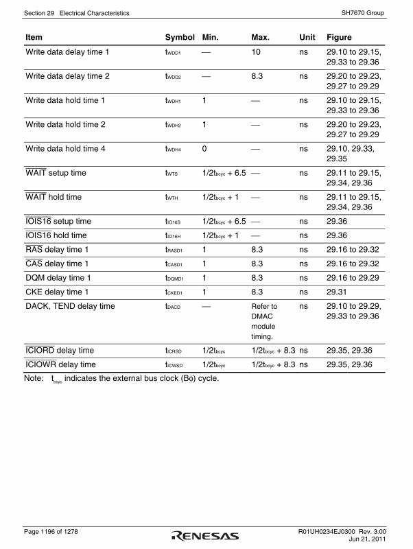
Section 29 Electrical Characteristics
Page 1196 of 1278 R01UH0234EJ0300 Rev. 3.00 Jun 21, 2011
SH7670 Group
Item Symbol Min. Max. Unit Figure
Write data delay time 1 tWDD1 ⎯ 10 ns 29.10 to 29.15, 29.33 to 29.36
Write data delay time 2 tWDD2 ⎯ 8.3 ns 29.20 to 29.23, 29.27 to 29.29
Write data hold time 1 tWDH1 1 ⎯ ns 29.10 to 29.15, 29.33 to 29.36
Write data hold time 2 tWDH2 1 ⎯ ns 29.20 to 29.23, 29.27 to 29.29
Write data hold time 4 tWDH4 0 ⎯ ns 29.10, 29.33, 29.35
WAIT setup time tWTS 1/2tbcyc + 6.5 ⎯ ns 29.11 to 29.15, 29.34, 29.36
WAIT hold time tWTH 1/2tbcyc + 1 ⎯ ns 29.11 to 29.15, 29.34, 29.36
IOIS16 setup time tIO16S 1/2tbcyc + 6.5 ⎯ ns 29.36
IOIS16 hold time tIO16H 1/2tbcyc + 1 ⎯ ns 29.36
RAS delay time 1 tRASD1 1 8.3 ns 29.16 to 29.32
CAS delay time 1 tCASD1 1 8.3 ns 29.16 to 29.32
DQM delay time 1 tDQMD1 1 8.3 ns 29.16 to 29.29
CKE delay time 1 tCKED1 1 8.3 ns 29.31
DACK, TEND delay time tDACD ⎯ Refer to DMAC module timing.
ns 29.10 to 29.29, 29.33 to 29.36
ICIORD delay time tICRSD 1/2tbcyc 1/2tbcyc + 8.3 ns 29.35, 29.36
ICIOWR delay time tICWSD 1/2tbcyc 1/2tbcyc + 8.3 ns 29.35, 29.36
Note: tbcyc indicates the external bus clock (Bφ) cycle.

Section 29 Electrical Characteristics
R01UH0234EJ0300 Rev. 3.00 Page 1197 of 1278 Jun 21, 2011
SH7670 Group
T1
tAD1
tAS
tCSD1
T2
tAD1
tRWD1 tRWD1
tCSD1
tRSD tRSD tAH
tRDH1
tRDS1
tWED1 tWED1 tAH
tBSD tBSD
tDACD tDACD
tWDH4
tWDD1
CKIO
A25 to A0
CSn
RD/WR
RD
D31 to D0
Read
WEn
BS
DACKnTENDn*
Note: * The waveforms for DACKn and TENDn are produced when the active low state is specified.
D31 to D0
Write tWDH1
Figure 29.10 Basic Bus Timing for Normal Space (No Wait)

Section 29 Electrical Characteristics
Page 1198 of 1278 R01UH0234EJ0300 Rev. 3.00 Jun 21, 2011
SH7670 Group
T1
tAD1
tAS
tCSD1
Tw T2
tAD1
tRWD1 tRWD1
tCSD1
tRSD tRSD tAH
tRDS1
tWED1 tWED1 tAH
tBSD tBSD
tWTH
tWTS
tDACD tDACD
tWDH1tWDD1
CKIO
A25 to A0
CSn
RD/WR
RD
D31 to D0
Read
WEn
BS
WAIT
DACKnTENDn*
Note: * The waveforms for DACKn and TENDn are produced when the active low state is specified.
D31 to D0
Write
tRDH1
Figure 29.11 Basic Bus Timing for Normal Space (One Software Wait Cycle)
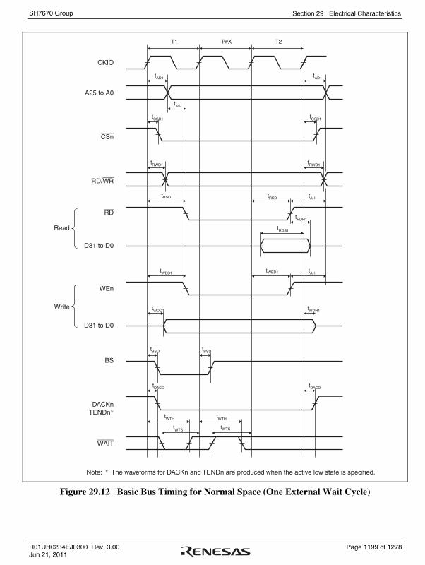
Section 29 Electrical Characteristics
R01UH0234EJ0300 Rev. 3.00 Page 1199 of 1278 Jun 21, 2011
SH7670 Group
T1
tAD1
tAS
tCSD1
TwX T2
tAD1
tRWD1 tRWD1
tCSD1
tRSD tRSD tAH
tRDS1
tWED1 tWED1 tAH
tBSD tBSD
tWTH
tWTS
tWTH
tWTS
tDACD tDACD
tWDH1tWDD1
CKIO
A25 to A0
CSn
RD/WR
RD
D31 to D0
Read
WEn
BS
WAIT
DACKnTENDn*
Note: * The waveforms for DACKn and TENDn are produced when the active low state is specified.
D31 to D0
Write
tRDH1
Figure 29.12 Basic Bus Timing for Normal Space (One External Wait Cycle)

Section 29 Electrical Characteristics
Page 1200 of 1278 R01UH0234EJ0300 Rev. 3.00 Jun 21, 2011
SH7670 Group
tAD1 tAD1
T1
tRWD1
tRSD
tWED1 tWED1 tWED1
tRDS1 tRDS1
tAS
tRSD tRSDtAHtRSD
tAH tWED1 tAH
tAH
tCSD1
tWDD1 tWDH1 tWDH1tWDD1
tBSD tBSD
tDACD tDACD tDACDtDACD
tBSD tBSD
tRWD1 tRWD1 tRWD1
tCSD1 tCSD1tCSD1
tAS
tAD1 tAD1
Tw T2 Taw T1 Tw T2 Taw
DACKnTENDn*
Note: * The waveforms for DACKn and TENDn are produced when the active low state is specified.
A25 to A0
D31 to D0
CSn
RD/WR
RD
WAIT
D31 to D0
WEn
BS
CKIO
tWTH
tWTS
tWTH
tWTS
tRDH1 tRDH1
Read
Write
Figure 29.13 Basic Bus Timing for Normal Space (One Software Wait Cycle, External Wait Enabled (WM Bit = 0), No Idle Cycle)

Section 29 Electrical Characteristics
R01UH0234EJ0300 Rev. 3.00 Page 1201 of 1278 Jun 21, 2011
SH7670 Group
Th
tAD1
tRSD tRSD
tRDS1
tCSD1
tRWD1
T1 Twx T2 Tf
tWDD1
tBSD
tWDH1
tRDH1
tAD1
tCSD1
CKIO
A25 to A0
CSn
WEn
RD
D31 to D0
D31 to D0
Read
RD/WR
RD/WR
BS
WAIT
DACKnTENDn*
Note: * The waveforms for DACKn and TENDn are produced when the active low state is specified.
Write
tDACD tDACD
tBSD
tWTS tWTS
tRWD1
tRWD1 tRWD1
tWED1 tWED1
tWTH tWTH
Figure 29.14 SRAM Bus Cycle with Byte Selection (SW = One Cycle, HW = One Cycle, One Asynchronous External Wait Cycle, BAS = 0 (Write Cycle UB/LB Control))

Section 29 Electrical Characteristics
Page 1202 of 1278 R01UH0234EJ0300 Rev. 3.00 Jun 21, 2011
SH7670 Group
Th
tAD1
tRSD tRSD
tRDS1
tCSD1
T1 Twx T2 Tf
tRWD1
tWDD1
tBSD
tRWD1 tRWD1
tWDH1
tRDH1
tAD1
tCSD1
CKIO
A25 to A0
CSn
WEn
RD
D31 to D0
D31 to D0
Read
RD/WR
RD/WR
BS
WAIT
DACKnTENDn*
Note: * The waveforms for DACKn and TENDn are produced when the active low state is specified.
Write
tDACD tDACD
tBSD
tWTS tWTS
tWED2 tWED2
tRWD1
tWTH tWTH
Figure 29.15 SRAM Bus Cycle with Byte Selection (SW = One Cycle, HW = One Cycle, One Asynchronous External Wait Cycle, BAS = 1 (Write Cycle WE Control))

Section 29 Electrical Characteristics
R01UH0234EJ0300 Rev. 3.00 Page 1203 of 1278 Jun 21, 2011
SH7670 Group
Tc1Tr Tcw Td1 Tde
tAD1 tAD1
tCSD1
tAD1
tRWD1 tRWD1
tCSD1
tAD1 tAD1tAD1
tRDH2tRDS2
CKIO
A25 to A0
CSn
RD/WR
A12/A11*1
Notes: 1. Address pin to be connected to A10 of SDRAM 2. The waveforms for DACKn and TENDn are produced when the active low state is specified.
D31 to D0
tRASD1 tRASD1
RAS
Row address
READA command
Column address
tCASD1 tCASD1
CAS
tBSD tBSD
(High)
BS
CKE
tDQMD1 tDQMD1
DQMxx
tDACD tDACD
DACKnTENDn*2
Figure 29.16 Synchronous DRAM Single-Read Bus Cycle (Auto-Precharged, CAS Latency 2, WTRCD = Zero Cycle, WTRP = Zero Cycle)

Section 29 Electrical Characteristics
Page 1204 of 1278 R01UH0234EJ0300 Rev. 3.00 Jun 21, 2011
SH7670 Group
TrwTr Tc1 Tcw Td1 Tde Tap
tAD1 tAD1
tCSD1
tAD1
tRWD1 tRWD1
tCSD1
tAD1 tAD1tAD1
tRDH2tRDS2
CKIO
A25 to A0
CSn
RD/WR
A12/A11*1
Notes: 1. Address pin to be connected to A10 of SDRAM 2. The waveforms for DACKn and TENDn are produced when the active low state is specified.
D31 to D0
tRASD1 tRASD1
RAS
Row address
READA command
Column address
tCASD1 tCASD1
CAS
tBSD tBSD
(High)
BS
CKE
tDQMD1 tDQMD1
DQMxx
tDACD tDACD
DACKnTENDn*2
Figure 29.17 Synchronous DRAM Single-Read Bus Cycle (Auto-Precharged, CAS Latency 2, WTRCD = One Cycle, WTRP = One Cycle)
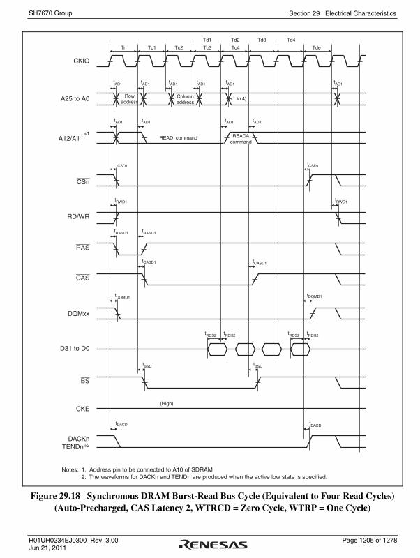
Section 29 Electrical Characteristics
R01UH0234EJ0300 Rev. 3.00 Page 1205 of 1278 Jun 21, 2011
SH7670 Group
Tc1 Tc2
Td1 Td2 Td3 Td4
Tr Tc3 Tc4 Tde
tAD1 tAD1
tCSD1
tAD1 tAD1 tAD1tAD1
tRWD1 tRWD1
tCSD1
tAD1 tAD1 tAD1 tAD1
tRDH2tRDS2
CKIO
A25 to A0
CSn
RD/WR
A12/A11*1
Notes: 1. Address pin to be connected to A10 of SDRAM 2. The waveforms for DACKn and TENDn are produced when the active low state is specified.
D31 to D0
tRASD1 tRASD1
RAS
Rowaddress
READAcommand
READ command
Columnaddress
(1 to 4)
tCASD1 tCASD1
CAS
tBSD tBSD
(High)
BS
CKE
tDQMD1 tDQMD1
DQMxx
tDACD tDACD
DACKnTENDn*2
tRDH2tRDS2
Figure 29.18 Synchronous DRAM Burst-Read Bus Cycle (Equivalent to Four Read Cycles) (Auto-Precharged, CAS Latency 2, WTRCD = Zero Cycle, WTRP = One Cycle)

Section 29 Electrical Characteristics
Page 1206 of 1278 R01UH0234EJ0300 Rev. 3.00 Jun 21, 2011
SH7670 Group
Tc1 Tc2
Td1 Td2 Td3 Td4
Tr Trw Tc3 Tc4 Tde
tAD1 tAD1
tCSD1
tAD1 tAD1 tAD1tAD1
tRWD1 tRWD1
tCSD1
tAD1 tAD1 tAD1 tAD1
tRDH2tRDS2
CKIO
A25 to A0
CSn
RD/WR
A12/A11*1
D31 to D0
tRASD1 tRASD1
RAS
Rowaddress
READ command
Columnaddress
(1 to 4)
tCASD1 tCASD1
CAS
tBSD tBSD
(High)
BS
CKE
tDQMD1 tDQMD1
DQMxx
tDACD tDACD
DACKnTENDn*2
tRDH2tRDS2
1. Address pin to be connected to A10 of SDRAM2. The waveforms for DACKn and TENDn are produced when the active low state is specified.
READA command
Notes:
Figure 29.19 Synchronous DRAM Burst-Read Bus Cycle (Equivalent to Four Read Cycles) (Auto-Precharged, CAS Latency 2, WTRCD = One Cycle, WTRP = Zero Cycle)

Section 29 Electrical Characteristics
R01UH0234EJ0300 Rev. 3.00 Page 1207 of 1278 Jun 21, 2011
SH7670 Group
TrwlTr Tc1
tAD1
tCSD1
tAD1 tAD1
tRWD1 tRWD1tRWD1
tCSD1
tAD1 tAD1 tAD1
CKIO
A25 to A0
CSn
RD/WR
A12/A11*1
D31 to D0
tRASD1 tRASD1
RAS
Rowaddress
WRITAcommand
Columnaddress
tCASD1 tCASD1
CAS
tBSD tBSD
(High)
BS
CKE
tDQMD1 tDQMD1
DQMxx
tDACD tDACD
DACKnTENDn*2
tWDH2tWDD2
Notes: 1. Address pin to be connected to A10 of SDRAM2. The waveforms for DACKn and TENDn are produced when the active low state is specified.
Figure 29.20 Synchronous DRAM Single-Write Bus Cycle (Auto-Precharged, TRWL = One Cycle)

Section 29 Electrical Characteristics
Page 1208 of 1278 R01UH0234EJ0300 Rev. 3.00 Jun 21, 2011
SH7670 Group
Trw Tc1 Trwl Tr Trw
tAD1
tCSD1
tAD1 tAD1
tRWD1 tRWD1tRWD1
tCSD1
tAD1 tAD1 tAD1
CKIO
A25 to A0
CSn
RD/WR
A12/A11*1
D31 to D0
tRASD1 tRASD1
RAS
Row address
WRITAcommand
Columnaddress
tCASD1 tCASD1
CAS
tBSD tBSD
(High)
BS
CKE
tDQMD1 tDQMD1
DQMxx
tDACD tDACD
DACKnTENDn*2
tWDH2tWDD2
1. Address pin to be connected to A10 of SDRAM2. The waveforms for DACKn and TENDn are produced when the active low state is specified.
Notes:
Figure 29.21 Synchronous DRAM Single-Write Bus Cycle (Auto-Precharged, WTRCD = Two Cycles, TRWL = One Cycle)

Section 29 Electrical Characteristics
R01UH0234EJ0300 Rev. 3.00 Page 1209 of 1278 Jun 21, 2011
SH7670 Group
Tc2 Tc3 Tc4 TrwlTr Tc1
tAD1
tCSD1
tAD1tAD1 tAD1tAD1tAD1
tRWD1 tRWD1tRWD1
tCSD1
tAD1 tAD1 tAD1 tAD1
CKIO
A25 to A0
CSn
RD/WR
A12/A11*1
D31 to D0
tRASD1 tRASD1
RAS
Rowaddress
WRITAcommand
WRIT command
Columnaddress
tCASD1 tCASD1
CAS
tBSD tBSD
(High)
BS
CKE
tDQMD1 tDQMD1
DQMxx
tDACD tDACD
DACKnTENDn*2
tWDH2tWDD2
1. Address pin to be connected to A10 of SDRAM2. The waveforms for DACKn and TENDn are produced when the active low state is specified.
tWDH2tWDD2
Notes:
Figure 29.22 Synchronous DRAM Burst-Write Bus Cycle (Equivalent to Four Write Cycles)
(Auto-Precharged, WTRCD = Zero Cycle, TRWL = One Cycle)

Section 29 Electrical Characteristics
Page 1210 of 1278 R01UH0234EJ0300 Rev. 3.00 Jun 21, 2011
SH7670 Group
Tc2 Tc3 Tc4 TrwlTr Tc1Trw
tAD1
tCSD1
tAD1tAD1tAD1 tAD1tAD1
tRWD1 tRWD1tRWD1
tCSD1
tAD1 tAD1 tAD1 tAD1
CKIO
A25 to A0
CSn
RD/WR
A12/A11*1
D31 to D0
tRASD1 tRASD1
RAS
Rowaddress
WRITAcommand
WRIT command
Columnaddress
tCASD1 tCASD1
CAS
tBSD tBSD
(High)
BS
CKE
tDQMD1 tDQMD1
DQMxx
tDACD tDACD
DACKnTENDn*2
tWDH2tWDD2
1. Address pin to be connected to A10 of SDRAM2. The waveforms for DACKn and TENDn are produced when the active low state is specified.
tWDH2tWDD2
Notes:
Figure 29.23 Synchronous DRAM Burst-Write Bus Cycle (Equivalent to Four Write Cycles)
(Auto-Precharged, WTRCD = One Cycle, TRWL = One Cycle)
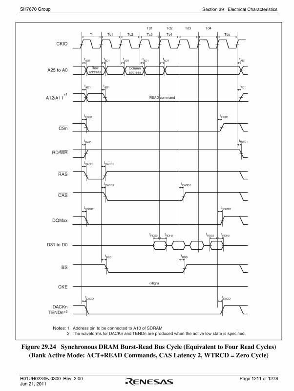
Section 29 Electrical Characteristics
R01UH0234EJ0300 Rev. 3.00 Page 1211 of 1278 Jun 21, 2011
SH7670 Group
Tc3 Tc4 TdeTr Tc2
Td1 Td2 Td3 Td4
Tc1
tCSD1
tAD1tAD1 tAD1 tAD1 tAD1tAD1
tRWD1 tRWD1
tCSD1
tAD1 tAD1 tAD1
CKIO
A25 to A0
CSn
RD/WR
A12/A11*1
D31 to D0
tRASD1 tRASD1
RAS
Rowaddress
READ command
Columnaddress
tCASD1 tCASD1
CAS
tBSD tBSD
(High)
BS
CKE
tDQMD1 tDQMD1
DQMxx
tDACD tDACD
DACKnTENDn*2
1. Address pin to be connected to A10 of SDRAM2. The waveforms for DACKn and TENDn are produced when the active low state is specified.
tRDH2tRDS2tRDH2tRDS2
Notes:
Figure 29.24 Synchronous DRAM Burst-Read Bus Cycle (Equivalent to Four Read Cycles) (Bank Active Mode: ACT+READ Commands, CAS Latency 2, WTRCD = Zero Cycle)

Section 29 Electrical Characteristics
Page 1212 of 1278 R01UH0234EJ0300 Rev. 3.00 Jun 21, 2011
SH7670 Group
Tc2 Tc4 TdeTc1 Tc3
Td1 Td2 Td3 Td4
tCSD1
tAD1tAD1 tAD1
tRWD1 tRWD1
tCSD1
tAD1tAD1
CKIO
A25 to A0
CSn
RD/WR
A12/A11*1
D31 to D0
tRASD1
RAS
READ command
Columnaddress
tCASD1 tCASD1
CAS
tBSD tBSD
(High)
BS
CKE
tDQMD1 tDQMD1
DQMxx
tDACD tDACD
DACKnTENDn*2
1. Address pin to be connected to A10 of SDRAM2. The waveforms for DACKn and TENDn are produced when the active low state is specified.
tRDH2tRDS2tRDH2tRDS2
Notes:
Figure 29.25 Synchronous DRAM Burst-Read Bus Cycle (Equivalent to Four Read Cycles) (Bank Active Mode: READ Command, Same Row Address, CAS Latency 2,
WTRCD = Zero Cycle)

Section 29 Electrical Characteristics
R01UH0234EJ0300 Rev. 3.00 Page 1213 of 1278 Jun 21, 2011
SH7670 Group
Tc3 Tc4 TdeTc2
Td1 Td2 Td3 Td4
Tc1TrTrwTp
tCSD1
tAD1 tAD1 tAD1 tAD1 tAD1 tAD1
tRWD1tRWD1 tRWD1
tCSD1
tAD1 tAD1 tAD1 tAD1
CKIO
A25 to A0
CSn
RD/WR
A12/A11*1
D31 to D0
tRASD1 tRASD1 tRASD1 tRASD1
RAS
READ command
Columnaddress
Rowaddress
tCASD1 tCASD1
CAS
tBSD tBSD
(High)
BS
CKE
tDQMD1 tDQMD1
DQMxx
tDACD tDACD
DACKnTENDn*2
1. Address pin to be connected to A10 of SDRAM2. The waveforms for DACKn and TENDn are produced when the active low state is specified.
tRDH2tRDS2tRDH2tRDS2
Notes:
Figure 29.26 Synchronous DRAM Burst-Read Bus Cycle (Equivalent to Four Read Cycles) (Bank Active Mode: PRE+ACT+READ Commands, Different Row Addresses,
CAS Latency 2, WTRCD = Zero Cycle)

Section 29 Electrical Characteristics
Page 1214 of 1278 R01UH0234EJ0300 Rev. 3.00 Jun 21, 2011
SH7670 Group
Tc2 Tc3 Tc4Tr Tc1
tAD1
tCSD1
tAD1tAD1tAD1 tAD1tAD1
tRWD1 tRWD1tRWD1
tCSD1
tAD1 tAD1 tAD1
CKIO
A25 to A0
CSn
RD/WR
A12/A11*1
D31 to D0
tRASD1 tRASD1
RAS
Rowaddress
WRIT command
Columnaddress
tCASD1 tCASD1
CAS
tBSD tBSD
(High)
BS
CKE
tDQMD1 tDQMD1
DQMxx
tDACD tDACD
DACKnTENDn*2
tWDH2tWDD2
Notes:
tWDH2tWDD2
1. Address pin to be connected to A10 of SDRAM2. The waveforms for DACKn and TENDn are produced when the active low state is specified.
Figure 29.27 Synchronous DRAM Burst-Write Bus Cycle (Equivalent to Four Write Cycles) (Bank Active Mode: ACT+WRITE Commands, WTRCD = Zero Cycle,
TRWL = Zero Cycle)
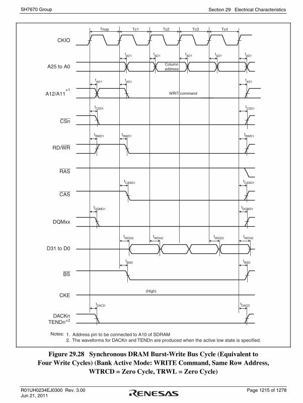
Section 29 Electrical Characteristics
R01UH0234EJ0300 Rev. 3.00 Page 1215 of 1278 Jun 21, 2011
SH7670 Group
Tc2 Tc3 Tc4Tnop Tc1
tAD1
tCSD1
tAD1tAD1tAD1tAD1
tRWD1 tRWD1tRWD1
tCSD1
tAD1 tAD1 tAD1
CKIO
A25 to A0
CSn
RD/WR
A12/A11*1
D31 to D0
RAS
WRIT command
Columnaddress
tCASD1 tCASD1
CAS
tBSD tBSD
(High)
BS
CKE
tDQMD1 tDQMD1
DQMxx
tDACD tDACD
DACKnTENDn*2
tWDH2tWDD2
1. Address pin to be connected to A10 of SDRAM2. The waveforms for DACKn and TENDn are produced when the active low state is specified.
tWDH2tWDD2
Notes:
Figure 29.28 Synchronous DRAM Burst-Write Bus Cycle (Equivalent to Four Write Cycles) (Bank Active Mode: WRITE Command, Same Row Address,
WTRCD = Zero Cycle, TRWL = Zero Cycle)

Section 29 Electrical Characteristics
Page 1216 of 1278 R01UH0234EJ0300 Rev. 3.00 Jun 21, 2011
SH7670 Group
Tc2 Tc3 Tc4TrTpwTp Tc1
tAD1
tCSD1
tAD1tAD1tAD1
tRWD1 tRWD1tRWD1 tRWD1
tCSD1
tRASD1tRASD1 tRASD1tRASD1
tAD1 tAD1 tAD1 tAD1
CKIO
A25 to A0
CSn
RD/WR
A12/A11*1
D31 to D0
RAS
WRIT command
Row address
tAD1 tAD1
Column address
tCASD1 tCASD1
CAS
tBSD tBSD
(High)
BS
CKE
tDQMD1 tDQMD1
DQMxx
tDACD tDACD
DACKnTENDn*2
tWDH2tWDD2
1. Address pin to be connected to A10 of SDRAM2. The waveforms for DACKn and TENDn are produced when the active low state is specified.
tWDH2tWDD2
Notes:
Figure 29.29 Synchronous DRAM Burst-Write Bus Cycle (Equivalent to Four Write Cycles) (Bank Active Mode: PRE+ACT+WRITE Commands, Different Row
Addresses, WTRCD = Zero Cycle, TRWL = Zero Cycle)

Section 29 Electrical Characteristics
R01UH0234EJ0300 Rev. 3.00 Page 1217 of 1278 Jun 21, 2011
SH7670 Group
Trc TrcTrrTpwTp Trc
tCSD1
tAD1tAD1
tRWD1 tRWD1 tRWD1
tCSD1 tCSD1 tCSD1
tRASD1tRASD1 tRASD1tRASD1
tAD1 tAD1
CKIO
A25 to A0
CSn
RD/WR
A12/A11*1
D31 to D0
RAS
tCASD1 tCASD1
CAS
(High)
(Hi-Z)
BS
CKE
DQMxx
DACKnTENDn*2
1. Address pin to be connected to A10 of SDRAM2. The waveforms for DACKn and TENDn are produced when the active low state is specified.
Notes:
Figure 29.30 Synchronous DRAM Auto-Refreshing Timing (WTRP = One Cycle, WTRC = Three Cycles)

Section 29 Electrical Characteristics
Page 1218 of 1278 R01UH0234EJ0300 Rev. 3.00 Jun 21, 2011
SH7670 Group
Trc Trc TrcTrrTpwTp
tCSD1
tAD1tAD1
tRWD1 tRWD1 tRWD1
tCSD1 tCSD1 tCSD1
tRASD1tRASD1 tRASD1tRASD1
tAD1 tAD1
CKIO
A25 to A0
CSn
RD/WR
A12/A11*1
D31 to D0
RAS
tCASD1 tCASD1
CAS
(Hi-Z)
BS
CKE
DQMxx
DACKnTENDn*2
1. Address pin to be connected to A10 of SDRAM2. The waveforms for DACKn and TENDn are produced when the active low state is specified.
tCKED1 tCKED1
Notes:
Figure 29.31 Synchronous DRAM Self-Refreshing Timing (WTRP = One Cycle)
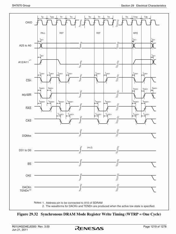
Section 29 Electrical Characteristics
R01UH0234EJ0300 Rev. 3.00 Page 1219 of 1278 Jun 21, 2011
SH7670 Group
Trc Trc Trc Tmw TdeTrrTrrTpwTp Trc
tCSD1
tAD1 tAD1tAD1
PALL REF REF MRS
tRWD1 tRWD1 tRWD1
tCSD1 tCSD1 tCSD1
tRASD1tRASD1 tRASD1tRASD1
tAD1 tAD1
CKIO
A25 to A0
CSn
RD/WR
A12/A11*1
D31 to D0
RAS
tCASD1 tCASD1
CAS
(Hi-Z)
BS
CKE
DQMxx
DACKnTENDn*2
1. Address pin to be connected to A10 of SDRAM2. The waveforms for DACKn and TENDn are produced when the active low state is specified.
tCSD1 tCSD1
tRASD1tRASD1
tCASD1 tCASD1
tCSD1 tCSD1
tRWD1 tRWD1
tRASD1tRASD1
tCASD1 tCASD1
Notes:
Figure 29.32 Synchronous DRAM Mode Register Write Timing (WTRP = One Cycle)

Section 29 Electrical Characteristics
Page 1220 of 1278 R01UH0234EJ0300 Rev. 3.00 Jun 21, 2011
SH7670 Group
Note: * The waveforms for DACKn and TENDn are produced when the active low state is specified.
CKIO
A25 to A0
CExx
RD/WR
RD
D15 to D0
WE
D15 to D0
BS
Read
Write
tAD1
tCSD1
tAD1
tCSD1
tRWD1
tWDH4
tBSD
tDACD
tBSD
DACKn
TENDn*
tDACD
tRDH1
Tpcm1w Tpcm2Tpcm1 Tpcm1w Tpcm1w
tRSD
tRDS1
tWED1
tRWD1
tWDD1
tRSD
tWED1
tWDH1
Figure 29.33 PCMCIA Memory Card Bus Cycle (TED = Zero Cycle, TEH = Zero Cycle, No Wait)
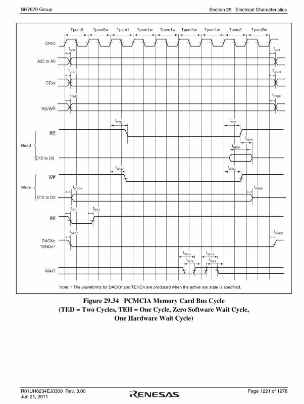
Section 29 Electrical Characteristics
R01UH0234EJ0300 Rev. 3.00 Page 1221 of 1278 Jun 21, 2011
SH7670 Group
CKIO
A25 to A0
CExx
RD/WR
RD
D15 to D0
WE
D15 to D0
BS
Read
Write
WAIT
tWTS
tAD1
tCSD1
tRWD1
tAD1
tCSD1
tRWD1
tBSD tBSD
Note: * The waveforms for DACKn and TENDn are produced when the active low state is specified.
DACKnTENDn*
tDACD tDACD
tWDH1tWDD1
tWED1tWED1
tRSDtRSD
tRDH1
tRDS1
tWTHtWTH
tWTS
Tpcm1w Tpcm2Tpcm0 Tpcm1 Tpcm1wTpcm0w Tpcm2wTpcm1w Tpcm1w
Figure 29.34 PCMCIA Memory Card Bus Cycle (TED = Two Cycles, TEH = One Cycle, Zero Software Wait Cycle,
One Hardware Wait Cycle)

Section 29 Electrical Characteristics
Page 1222 of 1278 R01UH0234EJ0300 Rev. 3.00 Jun 21, 2011
SH7670 Group
Note: * The waveforms for DACKn and TENDn are produced when the active low state is specified.
CKIO
A25 to A0
CExx
RD/WR
ICIORD
D15 to D0
ICIOWR
D15 to D0
BS
Read
Write
tAD1
tCSD1
tRWD1
tAD1
tCSD1
tRWD1
tWDD1
tWDH4
tBSD
tDACD
tBSD
DACKn
TENDn*
tDACD
tICRSD
tICWSD tICWSD
tRDH1
Tpcm1w Tpcm2Tpcm1 Tpcm1w Tpcm1w
tRDS1
tICRSD
tWDH1
Figure 29.35 PCMCIA I/O Card Bus Cycle (TED = Zero Cycle, TEH = Zero Cycle, No Wait)

Section 29 Electrical Characteristics
R01UH0234EJ0300 Rev. 3.00 Page 1223 of 1278 Jun 21, 2011
SH7670 Group
CKIO
A25 to A0
CExx
RD/WR
ICIORD
D15 to D0
ICIOWR
D15 to D0
BS
Read
Write
WAIT
tWTS
tAD1
tCSD1
tRWD1
tAD1
tCSD1
tRWD1
tBSD tBSD
Note: * The waveforms for DACKn and TENDn are produced when the active low state is specified.
DACKnTENDn*
tDACD tDACD
tWDH1tWDD1
tICWSDtICWSD
tICRSDtICRSD
tRDH1
tRDS1
tWTHtWTH
tWTS
IOIS16
Tpcm1w Tpcm2Tpcm0 Tpcm1 Tpcm1wTpcm0w Tpcm2wTpcm1w Tpcm1w
tIO16H
tIO16S
Figure 29.36 PCMCIA I/O Card Bus Cycle (TED = Two Cycles, TEH = One Cycle, Zero Software Wait Cycle,
One Hardware Wait Cycle)

Section 29 Electrical Characteristics
Page 1224 of 1278 R01UH0234EJ0300 Rev. 3.00 Jun 21, 2011
SH7670 Group
29.4.4 DMAC Module Timing
Table 29.9 DMAC Module Timing
Conditions: VCC = VCC (PLL) = DV12 = UV12 = 1.1 to 1.3 V, VCCQ = DV33 = 3.1 to 3.5 V, AV12 = 1.1 to 1.3 V, AV33 = 3.1 to 3.5 V, VSS = VSS (PLL) = DG12 = UG12 = VSSQ = DG33 = AG12 = AG33 = 0 V, Ta = –20 to 70°C (regular specifications), –40 to 85°C (wide temperature specifications)
Item Symbol Min. Max. Unit Figure
DREQ setup time tDRQS 10 ⎯
DREQ hold time tDRQH 10 ⎯
29.37
DACK, TEND delay time tDACD ⎯ 10
ns
29.38
tDRQS tDRQH
CKIO
DREQn
Note: n = 0, 1
Figure 29.37 DREQ Input Timing
Note: n = 0, 1
CKIO
TENDnDACKn
tDACD
tDACD
Figure 29.38 DACK, TEND Output Timing

Section 29 Electrical Characteristics
R01UH0234EJ0300 Rev. 3.00 Page 1225 of 1278 Jun 21, 2011
SH7670 Group
29.4.5 Watchdog Timer Timing
Table 29.10 shows the timing of the watchdog timer.
Table 29.10 Watchdog Timer Timing
Conditions: VCC = VCC (PLL) = DV12 = UV12 = 1.1 to 1.3 V, VCCQ = DV33 = 3.1 to 3.5 V, AV12 = 1.1 to 1.3 V, AV33 = 3.1 to 3.5 V, VSS = VSS (PLL) = DG12 = UG12 = VSSQ = DG33 = AG12 = AG33 = 0 V, Ta = –20 to 70°C (regular specifications), –40 to 85°C (wide temperature specifications)
Item Symbol Min. Max. Unit Figure
WDTOVF delay time tWOVD ⎯ 100 ns 29.39
tWOVDtWOVD
CKIO
WDTOVF
Figure 29.39 Watchdog Timer Timing

Section 29 Electrical Characteristics
Page 1226 of 1278 R01UH0234EJ0300 Rev. 3.00 Jun 21, 2011
SH7670 Group
29.4.6 SCIF Module Timing
Table 29.11 SCIF Module Timing
Conditions: VCC = VCC (PLL) = DV12 = UV12 = 1.1 to 1.3 V, VCCQ = DV33 = 3.1 to 3.5 V, AV12 = 1.1 to 1.3 V, AV33 = 3.1 to 3.5 V, VSS = VSS (PLL) = DG12 = UG12 = VSSQ = DG33 = AG12 = AG33 = 0 V, Ta = –20 to 70°C (regular specifications), –40 to 85°C (wide temperature specifications)
Item Symbol Min. Max. Unit Figure
Clocked synchronous 12 ⎯ tpcyc 29.40 Input clock cycle
Asynchronous
tScyc
4 ⎯ tpcyc 29.40
Input clock rise time tSCKr ⎯ 1.5 tpcyc 29.40
Input clock fall time tSCKf ⎯ 1.5 tpcyc 29.40
Input clock width tSCKW 0.4 0.6 tScyc 29.40
Transmit data delay time (Clocked synchronous)
tTXD ⎯ 3 × tpcyc +15 tpcyc 29.41
Receive data setup time (Clocked synchronous)
tRXS 4 × tpcyc +15 ⎯ ns 29.41
Receive data hold time (Clocked synchronous)
tRXH 100 ⎯ ns 29.41
Note: tpcyc indicates the peripheral clock (Pφ) cycle.
tSCKW tSCKr tSCKf
tScyc
SCK
Figure 29.40 SCK Input Clock Timing
tScyc
tTXD
SCK(input/output)
TxD(data transmit)
RxD(data receive)
tRXHtRXS
Figure 29.41 SCIF Input/Output Timing in Clocked Synchronous Mode

Section 29 Electrical Characteristics
R01UH0234EJ0300 Rev. 3.00 Page 1227 of 1278 Jun 21, 2011
SH7670 Group
29.4.7 IIC3 Module Timing
Table 29.12 I2C Bus Interface 3 Timing
Conditions: VCC = VCC (PLL) = DV12 = UV12 = 1.1 to 1.3 V, VCCQ = DV33 = 3.1 to 3.5 V, AV12 = 1.1 to 1.3 V, AV33 = 3.1 to 3.5 V, VSS = VSS (PLL) = DG12 = UG12 = VSSQ = DG33 = AG12 = AG33 = 0 V, Ta = –20 to 70°C (regular specifications), –40 to 85°C (wide temperature specifications)
Values
Item Symbol Test Conditions Min. Typ. Max. Unit Figure
SCL input cycle time tSCL 12 × tpcyc*1 + 600 ⎯ ⎯ ns
SCL input high pulse width tSCLH 3 × tpcyc*1 + 300 ⎯ ⎯ ns
SCL input low pulse width tSCLL 5 × tpcyc*1 + 300 ⎯ ⎯ ns
SCL, SDA input rise time tSr ⎯ ⎯ 300 ns
SCL, SDA input fall time tSf ⎯ ⎯ 300 ns
SCL, SDA input spike pulse removal time*2
tSP ⎯ ⎯ 1, 2 tpcyc*1
SDA input bus free time tBUF 5 ⎯ ⎯ tpcyc*1
Start condition input hold time tSTAH 3 ⎯ ⎯ tpcyc*1
Retransmit start condition input setup time
tSTAS 3 ⎯ ⎯ tpcyc*1
Stop condition input setup time tSTOS 3 ⎯ ⎯ tpcyc*1
Data input setup time tSDAS 1 × tpcyc*1 + 20 ⎯ ⎯ ns
Data input hold time tSDAH 0 ⎯ ⎯ ns
SCL, SDA capacitive load Cb 0 ⎯ 100 pF
SCL, SDA output fall time*3 tSf VCCQ = 3.1 to 3.5 V ⎯ ⎯ 250 ns
29.42
Notes: 1. tpcyc indicates the peripheral clock (Pφ) cycle.
2. Depends on the value of NF2CYC.
3. Indicates the I/O buffer characteristics.

Section 29 Electrical Characteristics
Page 1228 of 1278 R01UH0234EJ0300 Rev. 3.00 Jun 21, 2011
SH7670 Group
SCL
VIH
VIL
tSTAH
tBUF
P* S*
tSf tSr
tSCLtSDAH
tSCLH
tSCLL
SDA
Sr*
tSTAS
tSP tSTOS
tSDAS
P*
[Legend]S: Start conditionP: Stop conditionSr: Start condition for retransmission
Figure 29.42 I2C Bus Interface 3 Input/Output Timing

Section 29 Electrical Characteristics
R01UH0234EJ0300 Rev. 3.00 Page 1229 of 1278 Jun 21, 2011
SH7670 Group
29.4.8 SSI Module Timing
Table 29.13 SSI Module Timing
Conditions: VCC = VCC (PLL) = DV12 = UV12 = 1.1 to 1.3 V, VCCQ = DV33 = 3.1 to 3.5 V, AV12 = 1.1 to 1.3 V, AV33 = 3.1 to 3.5 V, VSS = VSS (PLL) = DG12 = UG12 = VSSQ = DG33 = AG12 = AG33 = 0 V, Ta = –20 to 70°C (regular specifications), –40 to 85°C (wide temperature specifications)
Item Symbol Min. Typ. Max. Unit Remarks Figure
Output clock cycle tO 80 ⎯ 6400 ns Output
Input clock cycle tI 80 ⎯ 6400 ns Input
Clock high tHC 32 ⎯ ⎯ ns
Clock low tLC 32 ⎯ ⎯ ns
Bidirectional
Clock rise time tRC ⎯ ⎯ 20 ns Output (100 pF)
29.43
Delay tDTR –5 ⎯ 25 ns Transmit 29.44, 29.45
Input setup time tSR 25 ⎯ ⎯ ns Receive 29.46, 29.47
Input hold time tHTR 5 ⎯ ⎯ ns Receive 29.46 to 29.47
AUDIO_CLK input frequency fAUDIO 10 ⎯ 40 MHz 29.48
tI ,tO
tHC
SSISCKntLC
tRC
Figure 29.43 Clock Input/Output Timing
tDTR tHTR
SSISCKn
SSIWSn, SSIDATAn
Figure 29.44 SSI Transmit Timing (1)
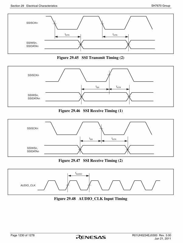
Section 29 Electrical Characteristics
Page 1230 of 1278 R01UH0234EJ0300 Rev. 3.00 Jun 21, 2011
SH7670 Group
tDTR tHTR
SSISCKn
SSIWSn, SSIDATAn
Figure 29.45 SSI Transmit Timing (2)
tSR tHTR
SSISCKn
SSIWSn, SSIDATAn
Figure 29.46 SSI Receive Timing (1)
tSR tHTR
SSISCKn
SSIWSn, SSIDATAn
Figure 29.47 SSI Receive Timing (2)
fAUDIO
AUDIO_CLK
Figure 29.48 AUDIO_CLK Input Timing

Section 29 Electrical Characteristics
R01UH0234EJ0300 Rev. 3.00 Page 1231 of 1278 Jun 21, 2011
SH7670 Group
29.4.9 USB Transceiver Timing
Table 29.14 USB Transceiver Timing (for Full Speed)
Conditions: VCC = VCC (PLL) = DV12 = UV12 = 1.1 to 1.3 V, VCCQ = DV33 = 3.1 to 3.5 V, AV12 = 1.1 to 1.3 V, AV33 = 3.1 to 3.5 V, VSS = VSS (PLL) = DG12 = UG12 = VSSQ = DG33 = AG12 = AG33 = 0 V, Ta = –20 to 70°C (regular specifications), –40 to 85°C (wide temperature specifications)
Item Symbol Min. Typ. Max. Unit Figure
Rise time tFR 4 ⎯ 20 ns
Fall time tFF 4 ⎯ 20 ns
Rise/fall time ratio tFR/tFF 70 ⎯ 130 %
29.49
DP, DM
tFR tFF
10% 10%90% 90%
Figure 29.49 DP/DM Output Timing (for Full Speed)
Circuit under measurement
DV33
DP
DM
DG33
CL 50pF
CL 50pFThe value of electrostatic capacitance (CL) includes the stray capacitance of the connection and the input capacitance of the probe.
Figure 29.50 Measurement Circuit (for Full Speed)

Section 29 Electrical Characteristics
Page 1232 of 1278 R01UH0234EJ0300 Rev. 3.00 Jun 21, 2011
SH7670 Group
Table 29.15 USB Transceiver Timing (for Low Speed)
Conditions: VCC = VCC (PLL) = DV12 = UV12 = 1.1 to 1.3 V, VCCQ = DV33 = 3.1 to 3.5 V, AV12 = 1.1 to 1.3 V, AV33 = 3.1 to 3.5 V, VSS = VSS (PLL) = DG12 = UG12 = VSSQ = DG33 = AG12 = AG33 = 0 V, Ta = –20 to 70°C (regular specifications), –40 to 85°C (wide temperature specifications)
Item Symbol Min. Typ. Max. Unit Figure
Rise time tLR 75 ⎯ 300 ns
Fall time tLF 75 ⎯ 300 ns
29.51
Output driver resistance tLR/tLF 80 ⎯ 125 %
DP, DM
tHSR tHSF
10% 10%90% 90%
Figure 29.51 DP/DM Output Timing (for Low Speed)
Circuit under measurement
DV33
DP
DM
DG33
RL 45Ω
RL 45Ω
Figure 29.52 Measurement Circuit (for Low Speed)
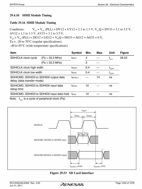
Section 29 Electrical Characteristics
R01UH0234EJ0300 Rev. 3.00 Page 1233 of 1278 Jun 21, 2011
SH7670 Group
29.4.10 SDHI Module Timing
Table 29.16 SDHI Module Timing
Conditions: VCC = VCC (PLL) = DV12 = UV12 = 1.1 to 1.3 V, VCCQ = DV33 = 3.1 to 3.5 V, AV12 = 1.1 to 1.3 V, AV33 = 3.1 to 3.5 V, VSS = VSS (PLL) = DG12 = UG12 = VSSQ = DG33 = AG12 = AG33 = 0 V, Ta = –20 to 70°C (regular specifications), –40 to 85°C (wide temperature specifications)
Item Symbol Min. Max. Unit Figure
(Pφ > 33.3 MHz) 4 ⎯ SDHICLK clock cycle
(Pφ ≤ 33.3 MHz)
tSDPP
2 ⎯
tpcyc
SDHICLK clock high width tSDWH 0.4 ⎯ tSDPP
SDHICLK clock low width tSDWL 0.4 ⎯ tSDPP
SDHICMD, SDHID3 to SDHID0 output data delay (data transfer mode)
tSDODLY ⎯ 14 ns
SDHICMD, SDHID3 to SDHID0 input data setup time
tSDISU 12 ⎯ ns
SDHICMD, SDHID3 to SDHID0 input data hold tSDIH 12 ⎯ ns
29.53
Note: tpcyc is a cycle of peripheral clock (Pφ).
tSDPP
tSDWL
tSDIHtSDISU
tSDODLY (max) tSDODLY (min)
tSDWH
SDHICLK
SDHICMD, SDHID3 to SDHID0 input
SDHICMD,SDHID3 to SDHID0 output
Figure 29.53 SD Card Interface

Section 29 Electrical Characteristics
Page 1234 of 1278 R01UH0234EJ0300 Rev. 3.00 Jun 21, 2011
SH7670 Group
29.4.11 I/O Port Timing
Table 29.17 I/O Port Timing
Conditions: VCC = VCC (PLL) = DV12 = UV12 = 1.1 to 1.3 V, VCCQ = DV33 = 3.1 to 3.5 V, AV12 = 1.1 to 1.3 V, AV33 = 3.1 to 3.5 V, VSS = VSS (PLL) = DG12 = UG12 = VSSQ = DG33 = AG12 = AG33 = 0 V, Ta = –20 to 70°C (regular specifications), –40 to 85°C (wide temperature specifications)
Item Symbol Min. Max. Unit Figure
Output data delay time tPORTD ⎯ 100
Input data setup time tPORTS 100 ⎯
Input data hold time tPORTH 100 ⎯
ns 29.54
tPORTS
CKIO
Port(read)
Port (write)
tPORTH
tPORTD
Figure 29.54 I/O Port Timing

Section 29 Electrical Characteristics
R01UH0234EJ0300 Rev. 3.00 Page 1235 of 1278 Jun 21, 2011
SH7670 Group
29.4.12 HIF Module Signal Timing
Table 29.18 HIF Module Signal Timing
Conditions: VCC = VCC (PLL) = DV12 = UV12 = 1.1 to 1.3 V, VCCQ = DV33 = 3.1 to 3.5 V, AV12 = 1.1 to 1.3 V, AV33 = 3.1 to 3.5 V, VSS = VSS (PLL) = DG12 = UG12 = VSSQ = DG33 = AG12 = AG33 = 0 V, Ta = –20 to 70°C (regular specifications), –40 to 85°C (wide temperature specifications)
Item Symbol Min. Max. Unit Figure
Read bus cycle time tHIFCYCR 5.0 ⎯ tpcyc
Write bus cycle time tHIFCYCW 5.0 ⎯ tpcyc
Read low width (in reading) tHIFWRL 3.0 ⎯ tpcyc
Write low width (in writing) tHIFWWL 3.0 ⎯ tpcyc
Read/write high width tHIFWRWH 2.0 ⎯ tpcyc
Read data delay time tHIFRDD ⎯ 2 × tpcyc + 16 ns
Read data hold time tHIFRDH 0 ⎯ ns
Write data setup time tHIFWDS tpcyc + 10 ⎯ ns
Write data hold time tHIFWDH 10 ⎯ ns
29.55
HIFINT output delay time tHIFITD ⎯ 20 ns 29.56
HIFRDY output delay time tHIFRYD ⎯ 20 tpcyc 29.57
HIFDREQ output delay time tHIFDQD ⎯ 20 ns 29.56
HIF pin enable delay time tHIFEBD ⎯ 20 ns 29.57
HIF pin disable delay time tHIFDBD ⎯ 20 ns 29.57
Notes: 1. tpcyc indicates the peripheral clock (Pφ) cycle.
2. The tHIFWRL period is specified as the overlap between the LOW period of the HIFCS signal and the LOW period of the HIFRD signal.
3. The tHIFWWL period is specified as the overlap between the LOW period of the HIFCS signal and the LOW period of the HIFWR signal.
4. The tHIFWRWH (min) is equal to 2 × tpcyc + 5 ns when writing into the HIF index register (HIFIDX) is followed by reading from the registers REG5 to REG0.

Section 29 Electrical Characteristics
Page 1236 of 1278 R01UH0234EJ0300 Rev. 3.00 Jun 21, 2011
SH7670 Group
HIFRS
HIFCS
HIFRD
HIFWR
HIFD15 to HIFD00
tHIFWRL
tHIFCYCR tHIFCYCW
tHIFWWL
tHIFWRWH
tHIFWDStHIFRDHtHIFRDD tHIFWDH
Read data Write data
Figure 29.55 HIF Access Timing
CKIO
HIFINT
HIFDREQ
tHIFDQD
tHIFITD
Figure 29.56 HIFINT/HIFDREQ Timing
tHIFDBD
tHIFRYD tHIFRYD
tHIFEBD
HIFD15 to HIFD0
HIFEBL
HIFINT
RES
HIFDREQHIFRDY
HIFRDY
Figure 29.57 HIFRDY/HIF Pin Enable/Disable Timing
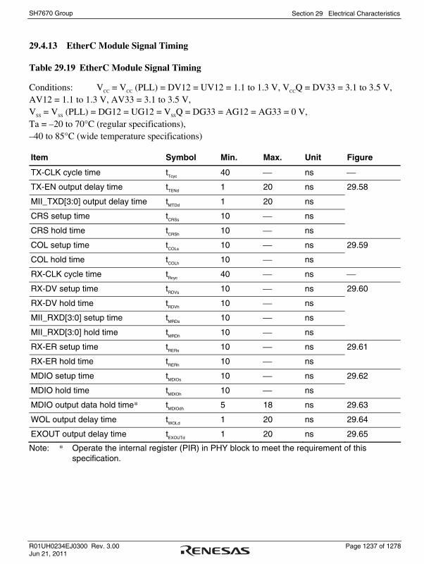
Section 29 Electrical Characteristics
R01UH0234EJ0300 Rev. 3.00 Page 1237 of 1278 Jun 21, 2011
SH7670 Group
29.4.13 EtherC Module Signal Timing
Table 29.19 EtherC Module Signal Timing
Conditions: VCC = VCC (PLL) = DV12 = UV12 = 1.1 to 1.3 V, VCCQ = DV33 = 3.1 to 3.5 V, AV12 = 1.1 to 1.3 V, AV33 = 3.1 to 3.5 V, VSS = VSS (PLL) = DG12 = UG12 = VSSQ = DG33 = AG12 = AG33 = 0 V, Ta = –20 to 70°C (regular specifications), –40 to 85°C (wide temperature specifications)
Item Symbol Min. Max. Unit Figure
TX-CLK cycle time tTcyc 40 ⎯ ns ⎯
TX-EN output delay time tTENd 1 20 ns
MII_TXD[3:0] output delay time tMTDd 1 20 ns
CRS setup time tCRSs 10 ⎯ ns
CRS hold time tCRSh 10 ⎯ ns
29.58
COL setup time tCOLs 10 ⎯ ns
COL hold time tCOLh 10 ⎯ ns
29.59
RX-CLK cycle time tRcyc 40 ⎯ ns ⎯
RX-DV setup time tRDVs 10 ⎯ ns
RX-DV hold time tRDVh 10 ⎯ ns
MII_RXD[3:0] setup time tMRDs 10 ⎯ ns
MII_RXD[3:0] hold time tMRDh 10 ⎯ ns
29.60
RX-ER setup time tRERs 10 ⎯ ns
RX-ER hold time tRERh 10 ⎯ ns
29.61
MDIO setup time tMDIOs 10 ⎯ ns
MDIO hold time tMDIOh 10 ⎯ ns
29.62
MDIO output data hold time* tMDIOdh 5 18 ns 29.63
WOL output delay time tWOLd 1 20 ns 29.64
EXOUT output delay time tEXOUTd 1 20 ns 29.65
Note: * Operate the internal register (PIR) in PHY block to meet the requirement of this specification.

Section 29 Electrical Characteristics
Page 1238 of 1278 R01UH0234EJ0300 Rev. 3.00 Jun 21, 2011
SH7670 Group
tCRSs tCRSh
tTENd
tETDd
TX-CLK
TX-EN
MII_TXD[3:0]
TX-ER
CRS
COL
DATASFD CRCPreamble
Figure 29.58 MII Transmit Timing (during Normal Operation)
tCOLhtCOLs
TX-CLK
TX-EN
MII_TXD[3:0]
TX-ER
CRS
COL
JAMPreamble
Figure 29.59 MII Transmit Timing (in the Event of a Collision)

Section 29 Electrical Characteristics
R01UH0234EJ0300 Rev. 3.00 Page 1239 of 1278 Jun 21, 2011
SH7670 Group
tRDVs tRDVh
tERDh
tERDs
RX-CLK
RX-DV
MII_RXD[3:0]
RX-ER
DATASFD CRCPreamble
Figure 29.60 MII Receive Timing (during Normal Operation)
tRERstRERh
RX-CLK
RX-DV
MII_RXD[3:0]
RX-ER
DATASFD xxxxPreamble
Figure 29.61 MII Receive Timing (in the Event of a Collision)
MDC
MDIO
tMDIOstMDIOh
Figure 29.62 MDIO Input Timing
MDC
MDIO
tMDIOdh
Figure 29.63 MDIO Output Timing
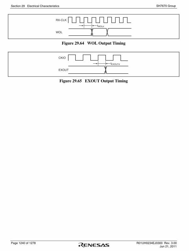
Section 29 Electrical Characteristics
Page 1240 of 1278 R01UH0234EJ0300 Rev. 3.00 Jun 21, 2011
SH7670 Group
RX-CLK
WOL
tWOLd
Figure 29.64 WOL Output Timing
CKIO
EXOUT
tEXOUTd
Figure 29.65 EXOUT Output Timing

Section 29 Electrical Characteristics
R01UH0234EJ0300 Rev. 3.00 Page 1241 of 1278 Jun 21, 2011
SH7670 Group
29.4.14 H-UDI Related Pin Timing
Table 29.20 H-UDI Related Pin Timing
Conditions: VCC = VCC (PLL) = DV12 = UV12 = 1.1 to 1.3 V, VCCQ = DV33 = 3.1 to 3.5 V, AV12 = 1.1 to 1.3 V, AV33 = 3.1 to 3.5 V, VSS = VSS (PLL) = DG12 = UG12 = VSSQ = DG33 = AG12 = AG33 = 0 V, Ta = –20 to 70°C (regular specifications), –40 to 85°C (wide temperature specifications)
Item Symbol Min. Max. Unit Figure
TCK cycle time tTCKcyc 50* ⎯ ns
TCK high pulse width tTCKH 0.4 0.6 tTCKcyc
TCK low pulse width tTCKL 0.4 0.6 tTCKcyc
29.66
TDI setup time tTDIS 10 ⎯ ns
TDI hold time tTDIH 10 ⎯ ns
TMS setup time tTMSS 10 ⎯ ns
TMS hold time tTMSH 10 ⎯ ns
TDO delay time tTDOD ⎯ 16 ns
29.67
Note: * This should be greater than the cycle time for the peripheral clock (Pφ).
tTCKcyc
VIH
1/2 VccQ 1/2 VccQ
VIH
VIL VIL
VIH
tTCKLtTCKH
Figure 29.66 TCK Input Timing

Section 29 Electrical Characteristics
Page 1242 of 1278 R01UH0234EJ0300 Rev. 3.00 Jun 21, 2011
SH7670 Group
TCK
TMS
TDI
TDO
TDO change timingafter the switching command is set
Initial value
tTDIS tTDIH
tTCKcyc
tTMSS tTMSH
tTDOD
tTDOD
Figure 29.67 H-UDI Data Transfer Timing

Section 29 Electrical Characteristics
R01UH0234EJ0300 Rev. 3.00 Page 1243 of 1278 Jun 21, 2011
SH7670 Group
29.4.15 STIF Module Signal Timing (1)
Table 29.21 STIF Module Signal Timing (1)
Conditions: VCC = VCC (PLL) = DV12 = UV12 = 1.1 to 1.3 V, VCCQ = DV33 = 3.1 to 3.5 V, AV12 = 1.1 to 1.3 V, AV33 = 3.1 to 3.5 V, VSS = VSS (PLL) = DG12 = UG12 = VSSQ = DG33 = AG12 = AG33 = 0 V, Ta = –20 to 70°C (regular specifications), –40 to 85°C (wide temperature specifications)
Item Symbol Min. Max. Unit Figure
Parallel mode 2 24 STn_CLKIN clock input cycle Serial mode
tST_CKIN_CYC
1.25 24
tbcyc*
Parallel mode 0.4 0.6 STn_CLKIN clock input high pulse width Serial mode
tST_CKIN_H
0.4 0.6
tST_CKIN_CYC
Parallel mode 0.4 0.6 STn_CLKIN clock input low pulse width Serial mode
tST_CKIN_L
04 0.6
tST_CKIN_CYC
Parallel mode ⎯ 2.75 STn_CLKIN clock input rise time Serial mode
tST_CKIN_r
⎯ 1.75
ns
Parallel mode ⎯ 2.75 STn_CLKIN clock input fall time Serial mode
tST_CKIN_f
⎯ 1.75
ns
29.68
Note: * tbcyc indicates the external bus clock (Bφ) cycle.
tST_CKIN_CYC
VIH
1/2 VccQ 1/2 VccQ
VIHVIH
VIL
VIH
VILVIL
STn_CLKIN input
VIL
tST_CKIN_L
tST_CKIN_f tST_CKIN_ftST_CKIN_r tST_CKIN_r
tST_CKIN_H tST_CKIN_H
Figure 29.68 STIF Module Signal Timing (1)

Section 29 Electrical Characteristics
Page 1244 of 1278 R01UH0234EJ0300 Rev. 3.00 Jun 21, 2011
SH7670 Group
29.4.16 STIF Module Signal Timing (2)
Table 29.22 STIF Module Signal Timing (2)
Conditions: VCC = VCC (PLL) = DV12 = UV12 = 1.1 to 1.3 V, VCCQ = DV33 = 3.1 to 3.5 V, AV12 = 1.1 to 1.3 V, AV33 = 3.1 to 3.5 V, VSS = VSS (PLL) = DG12 = UG12 = VSSQ = DG33 = AG12 = AG33 = 0 V, Ta = –20 to 70°C (regular specifications), –40 to 85°C (wide temperature specifications)
Item Symbol Min. Max. Unit Figure
Parallel mode 2 24 ST_CLKOUT clock output cycle Serial mode
tST_CKOUT_CYC
1 24
tbcyc*
Parallel mode 6.75 ⎯ ST_CLKOUT clock output high pulse width Serial mode
tST_CKOUT_H
3 ⎯
ns
Parallel mode 6.75 ⎯ ST_CLKOUT clock output low pulse width Serial mode
tST_CKOUT_L
3 ⎯
ns
Parallel mode ⎯ 2.75 ST_CLKOUT clock output rise time Serial mode
tST_CKOUT_r
⎯ 2.75
ns
Parallel mode ⎯ 2.75 ST_CLKOUT clock output fall time Serial mode
tST_CKOUT_f
⎯ 2.75
ns
29.69
Note: * tbcyc indicates the external bus clock (Bφ) cycle.
tTS_CKOUT_CYC
VIH VIHVIH
VIL
VIH
VILVIL
ST_CLKOUT output
VIL
tST_CKOUT_L
tST_CKOUT_f tST_CKOUT_ftST_CKOUT_r tST_CKOUT_r
tST_CKOUT_H tST_CKOUT_H
1/2 VccQ 1/2 VccQ
Figure 29.69 STIF Module Signal Timing (2)
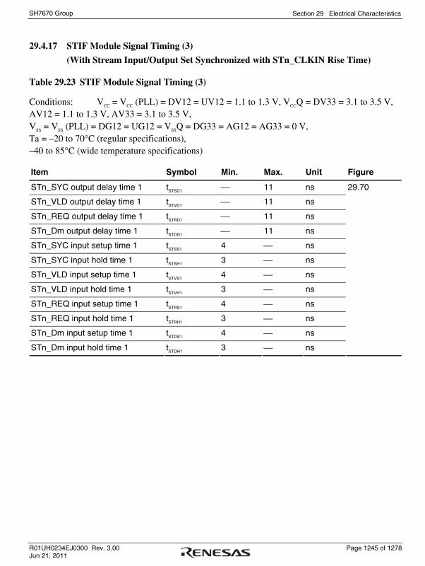
Section 29 Electrical Characteristics
R01UH0234EJ0300 Rev. 3.00 Page 1245 of 1278 Jun 21, 2011
SH7670 Group
29.4.17 STIF Module Signal Timing (3)
(With Stream Input/Output Set Synchronized with STn_CLKIN Rise Time)
Table 29.23 STIF Module Signal Timing (3)
Conditions: VCC = VCC (PLL) = DV12 = UV12 = 1.1 to 1.3 V, VCCQ = DV33 = 3.1 to 3.5 V, AV12 = 1.1 to 1.3 V, AV33 = 3.1 to 3.5 V, VSS = VSS (PLL) = DG12 = UG12 = VSSQ = DG33 = AG12 = AG33 = 0 V, Ta = –20 to 70°C (regular specifications), –40 to 85°C (wide temperature specifications)
Item Symbol Min. Max. Unit Figure
STn_SYC output delay time 1 tSTSD1 ⎯ 11 ns
STn_VLD output delay time 1 tSTVD1 ⎯ 11 ns
STn_REQ output delay time 1 tSTRD1 ⎯ 11 ns
STn_Dm output delay time 1 tSTDD1 ⎯ 11 ns
STn_SYC input setup time 1 tSTSS1 4 ⎯ ns
STn_SYC input hold time 1 tSTSH1 3 ⎯ ns
STn_VLD input setup time 1 tSTVS1 4 ⎯ ns
STn_VLD input hold time 1 tSTVH1 3 ⎯ ns
STn_REQ input setup time 1 tSTRS1 4 ⎯ ns
STn_REQ input hold time 1 tSTRH1 3 ⎯ ns
STn_Dm input setup time 1 tSTDS1 4 ⎯ ns
STn_Dm input hold time 1 tSTDH1 3 ⎯ ns
29.70

Section 29 Electrical Characteristics
Page 1246 of 1278 R01UH0234EJ0300 Rev. 3.00 Jun 21, 2011
SH7670 Group
STn_CLKIN input
STn_SYC output
STn_VLD output
STn_D7 - STn_D0 output
STn_SYC input
STn_VLD input
STn_D7 - STn_D0 input
tSTVD1
tSTSD1
tSTDD1
tSTVD1
tSTSD1
tSTDD1
tSTSS1
tSTVS1
tSTDS1
tSTSH1
tSTVH1
tSTDH1
tSTSS1
tSTVS1
tSTDS1
tSTSH1
tSTVH1
tSTDH1
STn_REQ input
tSTRS1 tSTRH1 tSTRS1 tSTRH1
Figure 29.70 STIF Module Signal Timing (3)

Section 29 Electrical Characteristics
R01UH0234EJ0300 Rev. 3.00 Page 1247 of 1278 Jun 21, 2011
SH7670 Group
29.4.18 STIF Module Signal Timing (4)
(With Stream Input/Output Set Synchronized with STn_CLKIN Fall Time)
Table 29.24 STIF Module Signal Timing (4)
Conditions: VCC = VCC (PLL) = DV12 = UV12 = 1.1 to 1.3 V, VCCQ = DV33 = 3.1 to 3.5 V, AV12 = 1.1 to 1.3 V, AV33 = 3.1 to 3.5 V, VSS = VSS (PLL) = DG12 = UG12 = VSSQ = DG33 = AG12 = AG33 = 0 V, Ta = –20 to 70°C (regular specifications), –40 to 85°C (wide temperature specifications)
Item Symbol Min. Max. Unit Figure
STn_SYC output delay time 2 tSTSD2 ⎯ 11 ns
STn_VLD output delay time 2 tSTVD2 ⎯ 11 ns
STn_REQ output delay time 2 tSTRD2 ⎯ 11 ns
STn_Dm output delay time 2 tSTDD2 ⎯ 11 ns
STn_SYC input setup time 2 tSTSS2 4 ⎯ ns
STn_SYC input hold time 2 tSTSH2 3 ⎯ ns
STn_VLD input setup time 2 tSTVS2 4 ⎯ ns
STn_VLD input hold time 2 tSTVH2 3 ⎯ ns
STn_REQ input setup time 2 tSTRS2 4 ⎯ ns
STn_REQ input hold time 2 tSTRH2 3 ⎯ ns
STn_Dm input setup time 2 tSTDS2 4 ⎯ ns
STn_Dm input hold time 2 tSTDH2 3 ⎯ ns
29.71

Section 29 Electrical Characteristics
Page 1248 of 1278 R01UH0234EJ0300 Rev. 3.00 Jun 21, 2011
SH7670 Group
tSTVD2
tSTSD2
tSTDD2
tSTVD2
tSTSD2
tSTDD2
tSTSS2
tSTVS2
tSTDS2
tSTSH2
tSTVH2
tSTDH2
tSTSS2
tSTVS2
tSTDS2
tSTSH2
tSTVH2
tSTDH2
tSTRS2 tSTRH2 tSTRS2 tSTRH2
STn_CLKIN input
STn_SYC output
STn_VLD output
STn_D7 - STn_D0 output
STn_SYC input
STn_VLD input
STn_D7 - STn_D0 input
STn_REQ input
Figure 29.71 STIF Module Signal Timing (4)

Section 29 Electrical Characteristics
R01UH0234EJ0300 Rev. 3.00 Page 1249 of 1278 Jun 21, 2011
SH7670 Group
29.4.19 STIF Module Signal Timing (5)
(With Stream Output Set Synchronized with STn_CLKOUT Rise Time)
Table 29.25 STIF Module Signal Timing (5)
Conditions: VCC = VCC (PLL) = DV12 = UV12 = 1.1 to 1.3 V, VCCQ = DV33 = 3.1 to 3.5 V, AV12 = 1.1 to 1.3 V, AV33 = 3.1 to 3.5 V, VSS = VSS (PLL) = DG12 = UG12 = VSSQ = DG33 = AG12 = AG33 = 0 V, Ta = –20 to 70°C (regular specifications), –40 to 85°C (wide temperature specifications)
Item Symbol Min. Max. Unit Figure
STn_SYC output delay time 5 tSTSD5 ⎯ 5 ns
STn_VLD output delay time 5 tSTVD5 ⎯ 5 ns
STn_Dm output delay time 5 tSTDD5 ⎯ 5 ns
STn_REQ input setup time 5 tSTRS5 8.5 ⎯ ns
STn_REQ input hold time 5 tSTRH5 0.5 ⎯ ns
29.72
STn_REQ input
tSTRH6tSTRS6 tSTRH6tSTRS6
ST_CLKOUT output
STn_SYC output
STn_VLD output
STn_D7 - STn_D0 output
tSTVD6
tSTSD6
tSTDD6
tSTVD6
tSTSD6
tSTDD6
Figure 29.72 STIF Module Signal Timing (5)
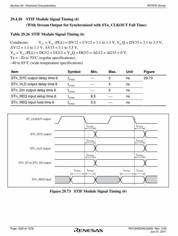
Section 29 Electrical Characteristics
Page 1250 of 1278 R01UH0234EJ0300 Rev. 3.00 Jun 21, 2011
SH7670 Group
29.4.20 STIF Module Signal Timing (6)
(With Stream Output Set Synchronized with STn_CLKOUT Fall Time)
Table 29.26 STIF Module Signal Timing (6)
Conditions: VCC = VCC (PLL) = DV12 = UV12 = 1.1 to 1.3 V, VCCQ = DV33 = 3.1 to 3.5 V, AV12 = 1.1 to 1.3 V, AV33 = 3.1 to 3.5 V, VSS = VSS (PLL) = DG12 = UG12 = VSSQ = DG33 = AG12 = AG33 = 0 V, Ta = –20 to 70°C (regular specifications), –40 to 85°C (wide temperature specifications)
Item Symbol Min. Max. Unit Figure
STn_SYC output delay time 6 tSTSD6 ⎯ 5 ns
STn_VLD output delay time 6 tSTVD6 ⎯ 5 ns
STn_Dm output delay time 6 tSTDD6 ⎯ 5 ns
STn_REQ input setup time 6 tSTRS6 8.5 ⎯ ns
STn_REQ input hold time 6 tSTRH6 0.5 ⎯ ns
29.73
ST_CLKOUT output
STn_SYC output
STn_VLD output
STn_D7 to STn_D0 output
tSTVD6
tSTSD6
tSTDD6
tSTVD6
tSTSD6
tSTDD6
STn_REQ input
tSTRH6tSTRS6 tSTRH6tSTRS6
Figure 29.73 STIF Module Signal Timing (6)

Section 29 Electrical Characteristics
R01UH0234EJ0300 Rev. 3.00 Page 1251 of 1278 Jun 21, 2011
SH7670 Group
29.4.21 STIF Module Signal Timing (7)
Table 29.27 STIF Module Signal Timing (7)
Conditions: VCC = VCC (PLL) = DV12 = UV12 = 1.1 to 1.3 V, VCCQ = DV33 = 3.1 to 3.5 V, AV12 = 1.1 to 1.3 V, AV33 = 3.1 to 3.5 V, VSS = VSS (PLL) = DG12 = UG12 = VSSQ = DG33 = AG12 = AG33 = 0 V, Ta = –20 to 70°C (regular specifications), –40 to 85°C (wide temperature specifications)
Item Symbol Min. Max. Unit Figure
STn_PWM output delay time tSTPWD ⎯ 15 ns 29.74
CKIO output
STn_PWM output
tSTPWD tSTPWDtSTPWD tSTPWD
Figure 29.74 STIF Module Signal Timing (7)
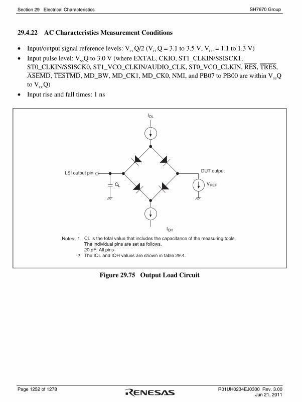
Section 29 Electrical Characteristics
Page 1252 of 1278 R01UH0234EJ0300 Rev. 3.00 Jun 21, 2011
SH7670 Group
29.4.22 AC Characteristics Measurement Conditions
• Input/output signal reference levels: VCCQ/2 (VCCQ = 3.1 to 3.5 V, VCC = 1.1 to 1.3 V)
• Input pulse level: VSSQ to 3.0 V (where EXTAL, CKIO, ST1_CLKIN/SSISCK1, ST0_CLKIN/SSISCK0, ST1_VCO_CLKIN/AUDIO_CLK, ST0_VCO_CLKIN, RES, TRES, ASEMD, TESTMD, MD_BW, MD_CK1, MD_CK0, NMI, and PB07 to PB00 are within VSSQ to VCCQ)
• Input rise and fall times: 1 ns
IOL
IOH
CL VREF
LSI output pin DUT output
Notes: CL is the total value that includes the capacitance of the measuring tools. The individual pins are set as follows.20 pF: All pinsThe IOL and IOH values are shown in table 29.4.
1.
2.
Figure 29.75 Output Load Circuit

Appendix
R01UH0234EJ0300 Rev. 3.00 Page 1253 of 1278 Jun 21, 2011
SH7670 Group
Appendix
A. Pin States
Pin Function Pin State
Type Pin Name Reset State Power-Down State
Power-On Reset (Non-HIF Boot Mode)
Power-On Reset (HIF Boot Mode)
Software Standby
Sleep
H-UDI Module Standby
Clock EXTAL EX/OS*1 EX/OS*1 XZ EX/OS*1 EX/OS*1
XTAL O/OS*1 O/OS*1 XZ O/OS*1 O/OS*1
CKIO I/O/Z*1 I/O/Z*1 Z I/O/Z*1*2 I I/O/Z*1*2
RES I I I I I System control WDTOVF H H O O O
TESTMD I I I I I
MD_BW I I I I I
MD_CK1 I I I I I
Operating mode control
MD_CK0 I I I I I
Interrupt NMI I I I I I
IRQ[7:0] — — I I I
Address bus
A[25:17] — — Z*4 O O
A[16:0] O O Z*4 O O
Data bus D[31:0] Z Z Z I/O I/O
Bus control
WAIT — — I I I
IOIS16 — — I I I
CKE Z Z Z*5 O O
CAS RAS Z Z Z*5 O O
WE0/DQMLL Z Z Z*4 O O
WE1/DQMLU/WE Z Z Z*4 O O
WE2/DQMUL/ ICIORD
Z Z Z*4 O O
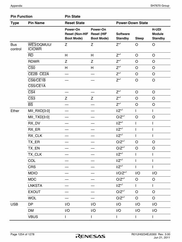
Appendix
Page 1254 of 1278 R01UH0234EJ0300 Rev. 3.00 Jun 21, 2011
SH7670 Group
Pin Function Pin State
Type Pin Name Reset State Power-Down State
Power-On Reset (Non-HIF Boot Mode)
Power-On Reset (HIF Boot Mode)
Software Standby
Sleep
H-UDI Module Standby
Bus control
WE3/DQMUU/ ICIOWR
Z Z Z*4 O O
RD H H Z*4 O O
RDWR Z Z Z*4 O O
CS0 H H Z*4 O O
CE2B CE2A — — Z*4 O O
CS6/CE1B
CS5/CE1A
— — Z*4 O O
CS4 — — Z*4 O O
CS3 Z Z Z*4 O O
BS — — Z*4 O O
Ether MII_RXD[3:0] — — I/Z*3 I I
MII_TXD[3:0] — — O/Z*3 O O
RX_DV — — I/Z*3 I I
RX_ER — — I/Z*3 I I
RX_CLK — — I/Z*3 I I
TX_ER — — O/Z*3 O O
TX_EN — — O/Z*3 O O
TX_CLK — — I/Z*3 I I
COL — — I/Z*3 I I
CRS — — I/Z*3 I I
MDIO — — I/O/Z*3 I/O I/O
MDC — — O/Z*3 O O
LNKSTA — — I/Z*3 I I
EXOUT — — O/Z*3 O O
WOL — — O/Z*3 O O
USB DP I/O I/O I/O I/O I/O
DM I/O I/O I/O I/O I/O
VBUS I I I I I
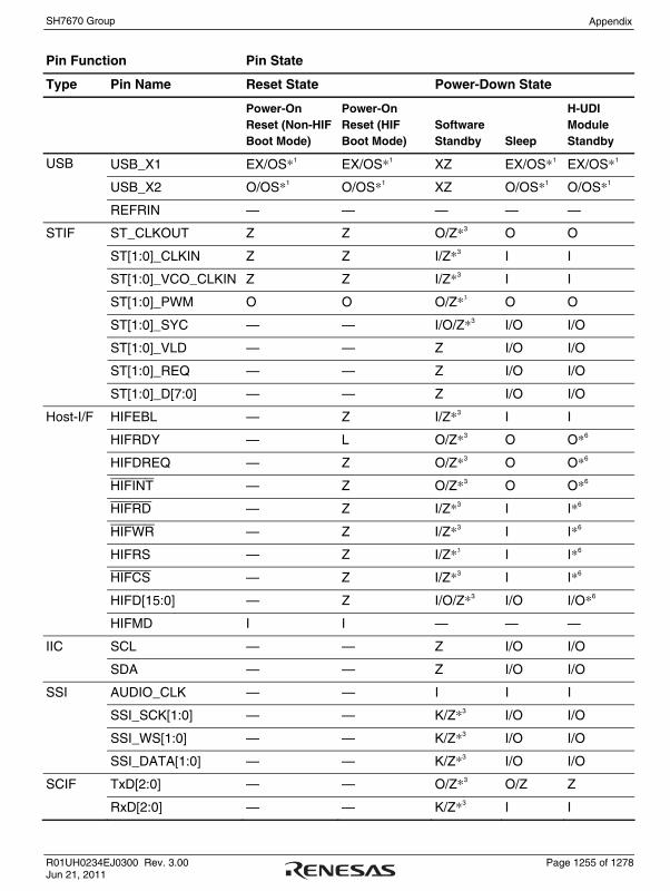
Appendix
R01UH0234EJ0300 Rev. 3.00 Page 1255 of 1278 Jun 21, 2011
SH7670 Group
Pin Function Pin State
Type Pin Name Reset State Power-Down State
Power-On Reset (Non-HIF Boot Mode)
Power-On Reset (HIF Boot Mode)
Software Standby
Sleep
H-UDI Module Standby
USB_X1 EX/OS*1 EX/OS*1 XZ EX/OS*1 EX/OS*1
USB_X2 O/OS*1 O/OS*1 XZ O/OS*1 O/OS*1
USB
REFRIN — — — — —
STIF ST_CLKOUT Z Z O/Z*3 O O
ST[1:0]_CLKIN Z Z I/Z*3 I I
ST[1:0]_VCO_CLKIN Z Z I/Z*3 I I
ST[1:0]_PWM O O O/Z*3 O O
ST[1:0]_SYC — — I/O/Z*3 I/O I/O
ST[1:0]_VLD — — Z I/O I/O
ST[1:0]_REQ — — Z I/O I/O
ST[1:0]_D[7:0] — — Z I/O I/O
Host-I/F HIFEBL — Z I/Z*3 I I
HIFRDY — L O/Z*3 O O*6
HIFDREQ — Z O/Z*3 O O*6
HIFINT — Z O/Z*3 O O*6
HIFRD — Z I/Z*3 I I*6
HIFWR — Z I/Z*3 I I*6
HIFRS — Z I/Z*3 I I*6
HIFCS — Z I/Z*3 I I*6
HIFD[15:0] — Z I/O/Z*3 I/O I/O*6
HIFMD I I — — —
IIC SCL — — Z I/O I/O
SDA — — Z I/O I/O
SSI AUDIO_CLK — — I I I
SSI_SCK[1:0] — — K/Z*3 I/O I/O
SSI_WS[1:0] — — K/Z*3 I/O I/O
SSI_DATA[1:0] — — K/Z*3 I/O I/O
SCIF TxD[2:0] — — O/Z*3 O/Z Z
RxD[2:0] — — K/Z*3 I I

Appendix
Page 1256 of 1278 R01UH0234EJ0300 Rev. 3.00 Jun 21, 2011
SH7670 Group
Pin Function Pin State
Type Pin Name Reset State Power-Down State
Power-On Reset (Non-HIF Boot Mode)
Power-On Reset (HIF Boot Mode)
Software Standby
Sleep
H-UDI Module Standby
SCK[2:0] — — K/Z*3 I/O I
RTS[2:0] — — K/Z*3 I/O I
SCIF
CTS[2:0] — — K/Z*3 I/O I/O
DMAC DACK[1:0] — — Z O O
DREQ[1:0] — — Z I I
TEND[1:0] — — Z O O
SDHI SDCLK — — O/Z*3 O O
SDCMD — — K/Z*3 I/O I/O
SDCD — — Z I I
SDWP — — Z I I
SDDAT[3:0] — — K/Z*3 I/O I/O
H-UDI TRST PI PI PI PI PI
TCK I I I I I
TMS PI PI PI PI PI
TDI PI PI PI PI PI
TDO Z Z Z Z Z
ASEBRK/ASEBRKAK I/PI*7 I/PI*7 I/PI*7 I/PI*7 I/PI*7
ASEMD I I I I I
[25] I I K/Z*3 I/O I/O I/O port PA[25:17]
[24:17] Z Z K/Z*3 I/O I/O
[01:00] I I I I/O I/O PB[07:00]
[07:02] Z Z K/Z*3 I/O I/O
PC[20:00] Z Z K/Z*3 I/O I/O
PD[07:00] I I K/Z*3 I/O I/O
[11] — — K/Z*3 I/O I/O PE[11:00]
[10:0] Z Z K/Z*3 I/O I/O
[11] — — K/Z*3 I/O I/O PF[11:00]
[10:0] Z Z K/Z*3 I/O I/O
PG[23:00] Z Z K/Z*3 I/O I/O
Appendix
R01UH0234EJ0300 Rev. 3.00 Page 1257 of 1278 Jun 21, 2011
SH7670 Group
[Legend]
—: This pin function is never selected as the initial state. I: Input
O: Output
EX: External clock input OS: Oscillated by a crystal oscillator
XZ: Standby state
H: High-level output L: Low-level output
Z: High-impedance
K: The pin retains its state. PI: Input enabled and pull-up state
Notes: 1. Depends on clock mode.
2. Depends on the setting of the CKOEN bits (bits 1 and 0) of the FRQCR register. 3. Depends on the settings of the IOR register bits of the general-purpose port and the
HIZ bit of the STBCR3 register. 4. Depends on the HIZMEM bit of the CMNCR register.
5. Depends on the HIZCNT bit of the CMNCR register.
6. High impedance when HIFEBL is set to the low level. 7. PI in non-ASE mode (when ASEMD = H input), I in ASE mode (when ASEMD = L
input).
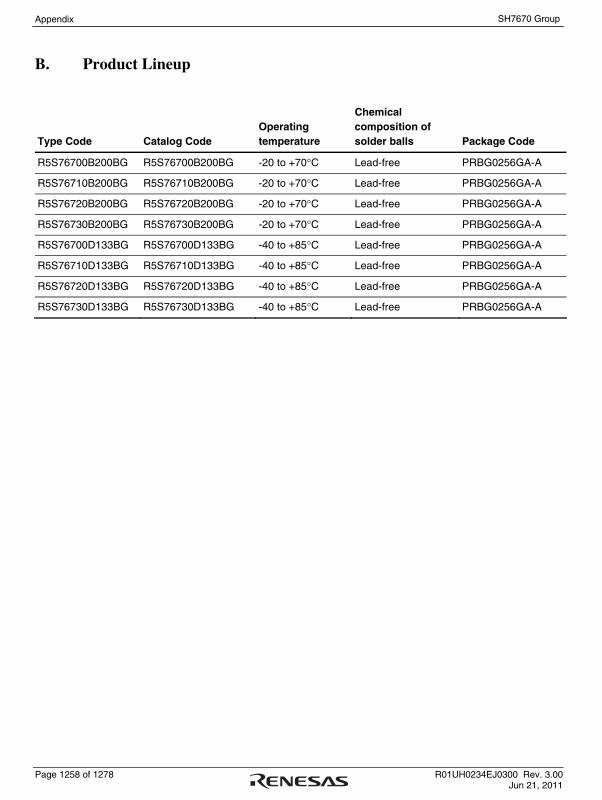
Appendix
Page 1258 of 1278 R01UH0234EJ0300 Rev. 3.00 Jun 21, 2011
SH7670 Group
B. Product Lineup
Type Code
Catalog Code
Operating temperature
Chemical composition of solder balls
Package Code
R5S76700B200BG R5S76700B200BG -20 to +70°C Lead-free PRBG0256GA-A
R5S76710B200BG R5S76710B200BG -20 to +70°C Lead-free PRBG0256GA-A
R5S76720B200BG R5S76720B200BG -20 to +70°C Lead-free PRBG0256GA-A
R5S76730B200BG R5S76730B200BG -20 to +70°C Lead-free PRBG0256GA-A
R5S76700D133BG R5S76700D133BG -40 to +85°C Lead-free PRBG0256GA-A
R5S76710D133BG R5S76710D133BG -40 to +85°C Lead-free PRBG0256GA-A
R5S76720D133BG R5S76720D133BG -40 to +85°C Lead-free PRBG0256GA-A
R5S76730D133BG R5S76730D133BG -40 to +85°C Lead-free PRBG0256GA-A

Appendix
R01UH0234EJ0300 Rev. 3.00 Page 1259 of 1278 Jun 21, 2011
SH7670 Group
C. Package Dimensions
e
A1
MaxNomMin
Dimension in MillimetersSymbol
Reference
A
b
x
y
17.0
0.10
0.80
0.45 0.50 0.55
0.35 0.40 0.45
1.90
17.0
0.08
v
w
0.9
0.9
y1 0.2
0.20
0.15
Previous CodeJEITA Package Code RENESAS Code0.85g
MASS[Typ.]
ZE
ZD
E
D
Z
Z
SE
SD
E
D
P-FBGA256-17x17-0.80 PRBG0256GA-A
1
1
A
A
B
S
Sy
Sw A Sw B
v
Sy 1
2 3 4 5 6 7 8 9 10 11 12 13 14 15 16 17 18 19 20
B
C
D
E
F
G
H
J
K
L
M
N
P
R
T
U
V
W
Y
A
A
e
e
BASφ × bφ
M
×4
D
E
⎯
Figure C.1 Package Dimensions

Appendix
Page 1260 of 1278 R01UH0234EJ0300 Rev. 3.00 Jun 21, 2011
SH7670 Group
D. Treatment of Unused Pins
Table D.1 Treatment of Unused Pins
Pin Functions Treatment of Unused Pins
Classification Symbol Non-HIF Boot Mode HIF Boot Mode
EXTAL Clock mode 0: These pins should be used.
Clock mode 1: These pins should be used.
Clock mode 2: Pull-up
Clock mode 3: Pull-up
Clock mode 0: These pins should be used.
Clock mode 1: These pins should be used.
Clock mode 2: Pull-up
Clock mode 3: Pull-up
XTAL Clock mode 0: These pins should be used.
Clock mode 1: These pins should be used.
Clock mode 2: Open
Clock mode 3: Open
Clock mode 0: These pins should be used.
Clock mode 1: These pins should be used.
Clock mode 2: Open
Clock mode 3: Open
Clock
CKIO Clock mode 0: Open
Clock mode 1: Open
Clock mode 2: These pins should be used.
Clock mode 3: Open
Clock mode 0: Open
Clock mode 1: Open
Clock mode 2: These pins should be used.
Clock mode 3: Open
RES These pins should be used. These pins should be used. System control
WDTOVF Open Open
TESTMD These pins should be used. These pins should be used.
MD_BW These pins should be used. These pins should be used.
MD_CK1 These pins should be used. These pins should be used.
Operating mode
control
MD_CK0 These pins should be used. These pins should be used.
NMI Pull-up Pull-up Interrupts
IRQ[7:0] ⎯ ⎯
A[25:17] ⎯ ⎯ Address bus
A[16:0] Open Open
Data bus D[31:0] Open Open
WAIT ⎯ ⎯
IOIS16 ⎯ ⎯
CKE Open Open
CAS, RAS Open Open
WE0/DQMLL Open Open
Bus control
WE1/DQMLU/
WE Open Open

Appendix
R01UH0234EJ0300 Rev. 3.00 Page 1261 of 1278 Jun 21, 2011
SH7670 Group
Pin Functions Treatment of Unused Pins
Classification Symbol Non-HIF Boot Mode HIF Boot Mode
WE2/DQMUL/
ICIORD Open Open
WE3/DQMUU/
ICIOWR Open Open
RD Open Open
RD/WR Open Open
CS0 Open Open
CE2B, CE2A ⎯ ⎯
CS6/CE1B ⎯ ⎯
CS5/CE1A ⎯ ⎯
CS4 ⎯ ⎯
CS3 Open Open
Bus control
BS ⎯ ⎯
MII_RXD[3:0] ⎯ ⎯
MII_TXD[3:0] ⎯ ⎯
RX_DV ⎯ ⎯
RX_ER ⎯ ⎯
RX_CLK ⎯ ⎯
TX_ER ⎯ ⎯
TX_EN ⎯ ⎯
TX_CLK ⎯ ⎯
COL ⎯ ⎯
CRS ⎯ ⎯
MDIO ⎯ ⎯
MDC ⎯ ⎯
LNKSTA ⎯ ⎯
EXOUT ⎯ ⎯
Ether
WOL ⎯ ⎯
DP These pins should be connected to DG33. These pins should be connected to DG33.
DM These pins should be connected to DG33. These pins should be connected to DG33.
USB
VBUS These pins should be connected to DG33. These pins should be connected to DG33.

Appendix
Page 1262 of 1278 R01UH0234EJ0300 Rev. 3.00 Jun 21, 2011
SH7670 Group
Pin Functions Treatment of Unused Pins
Classification Symbol Non-HIF Boot Mode HIF Boot Mode
USB_X1 Clock Mode 0: Pull-up
Clock Mode 1: Pull-up
Clock Mode 2: Pull-up
Clock Mode 3: These pins should be used.
Clock Mode 0: Pull-up
Clock Mode 1: Pull-up
Clock Mode 2: Pull-up
Clock Mode 3: These pins should be used.
USB_X2 Clock Mode 0: Open
Clock Mode 1: Open
Clock Mode 2: Open
Clock Mode 3: These pins should be
used. / Open
Clock Mode 0: Open
Clock Mode 1: Open
Clock Mode 2: Open
Clock Mode 3: These pins should be
used. / Open
USB
REFRIN ⎯ ⎯
ST_CLKOUT Open Open
ST[1:0]_CLKIN Pull-up Pull-up
ST[1:0]_
VCO_CLKIN
Pull-up Pull-up
ST[1:0]_PWM Open Open
ST[1:0]_SYC ⎯ ⎯
ST[1:0]_VLD ⎯ ⎯
ST[1:0]_REQ ⎯ ⎯
STIF
ST[1:0]_D[7:0] ⎯ ⎯
HIFEBL ⎯ These pins should be used.
HIFRDY ⎯ These pins should be used.
HIFDREQ ⎯ These pins should be used.
HIFINT ⎯ These pins should be used.
HIFRD ⎯ These pins should be used.
HIFWR ⎯ These pins should be used.
HIFRS ⎯ These pins should be used.
HIFCS ⎯ These pins should be used.
HIFD[15:0] ⎯ These pins should be used.
Host-I/F
HIFMD These pins should be used. These pins should be used.
SCL ⎯ ⎯ IIC
SDA ⎯ ⎯
AUDIO_CLK ⎯ ⎯
SSI_SCK[1:0] ⎯ ⎯
SSI
SSI_WS[1:0] ⎯ ⎯

Appendix
R01UH0234EJ0300 Rev. 3.00 Page 1263 of 1278 Jun 21, 2011
SH7670 Group
Pin Functions Treatment of Unused Pins
Classification Symbol Non-HIF Boot Mode HIF Boot Mode
SSI SSI_DATA[1:0] ⎯ ⎯
TxD[2:0] ⎯ ⎯
RxD[2:0] ⎯ ⎯
SCK[2:0] ⎯ ⎯
RTS[2:0] ⎯ ⎯
SCIF
CTS[2:0] ⎯ ⎯
DACK[1:0] ⎯ ⎯
DREQ[1:0] ⎯ ⎯
DMAC
TEND[1:0] ⎯ ⎯
SDCLK ⎯ ⎯
SDCMD ⎯ ⎯
SDCD ⎯ ⎯
SDWP ⎯ ⎯
SDHI
SDDAT[3:0] ⎯ ⎯
TRST These pins should be used. These pins should be used.
TCK Pull-up Pull-up
TMS Open Open
TDI Open Open
TDO Open Open
ASEBRK/ ASEBRKAK
Open Open
H-UDI
ASEMD These pins should be used. These pins should be used.
PA[25] These pins should be used. These pins should be used.
PA[24:17] Pull-up Pull-up
PB[01:00] Pull-up Pull-up
PB[07:02] Pull-up Pull-up
PC[20:00] Pull-up Pull-up
PD[07:00] Pull-up Pull-up
PE[11] ⎯ ⎯
PE[10:0] Pull-up Pull-up
PF[11] ⎯ ⎯
I/O port
PF[10:0] Pull-up Pull-up

Appendix
Page 1264 of 1278 R01UH0234EJ0300 Rev. 3.00 Jun 21, 2011
SH7670 Group
Pin Functions Treatment of Unused Pins
Classification Symbol Non-HIF Boot Mode HIF Boot Mode
I/O port PG[23:00] Pull-up ⎯
[Legend]
⎯: This pin function is not selected as the initial state.
R01UH0234EJ0300 Rev. 3.00 Page 1265 of 1278 Jun 21, 2011
Main Revisions and Additions in this Edition
Changes in Rev. 3.00 Compared to Rev. 2.00
Item Page Revision (See Manual for Details)
Table 1.1 Overview of SH7670 Group Specifications
5 Added
Classification Module/Function Description
External bus
extension
Bus state
controller (BSC)
• Address space for five areas (64
Mbytes each) and 32-bit external
bus
… …
• For area 0, only big endian is
supported
Figure 1.2 Block Diagram 13 Added
Figure 1.3 Pin Assignments 14 Amended
U4 pin: "VssQ_02" → "Vss_02"
Table 1.4 List of I/O Attributes of Each Pin
22, 24, 25
Amended
Pin Number Function Name I/O Attribute
A18 RAS O
D16 VSSQ_11 Power
G17 VCCQ_09 Power
G18 D31 IO
G19 D23 IO
G20 D22 IO
5.5.2 Interrupt Priority Level 123 Amended
The priority levels that can be set are 0 to 15. Level 16 cannot be set. See section 6.3.1, Interrupt Priority Registers 01, 02, 06 to 16 (IPR01, IPR02, IPR06 to IPR16), for details of IPR01, IPR02, and IPR06 to IPR16.
Table 5.9 Interrupt Priority Order
123 Amended
Type Priority Level
Comment
IRQ
On-chip peripheral module
0 to 15 Set with interrupt priority registers 01, 02, and 06 to 16 (IPR01, IPR02, and IPR06 to IPR16).

Page 1266 of 1278 R01UH0234EJ0300 Rev. 3.00 Jun 21, 2011
Item Page Revision (See Manual for Details)
Figure 6.1 Block Diagram of INTC
134 Amended
SDHI:IIC3:SCIF: ICR0:ICR1:ICR2:IRQRR:PINTER:PIRR:IBCR:IBNR:IPR01, IPR02, IPR06 to IPR16:
Module bus
IPR01, IPR02,IPR06 to IPR16
IPR
INTC
Businterface
Per
iphe
ral b
us
SD host interfaceI2C bus interface 3Serial communication interface with FIFO Interrupt control register 0Interrupt control register 1Interrupt control register 2IRQ interrupt request registerPINT interrupt enable registerPINT interrupt request registerBank control registerBank number registerInterrupt priority registers 01, 02, 06 to 16
7.1 Features 171 Added
⎯ For area 0, only big endian is supported.
7.4.2 CSn Space Bus Control Register (CSnBCR) (n = 0, 3 to 6)
184 Added
Bit Bit Name Description
11 ENDIAN Endian Setting
Specifies the arrangement of data in a space.
0: Arranged in big endian
1: Arranged in little endian
Note: Area 0 cannot be set to little endian mode. In the case of area 0, this bit is always read as 0, and the write value should always be 0.
7.4.3 CSn Space Wait Control Register (CSnWCR) (n = 0, 3 to 6)
(1) Normal Space, SRAM with Byte Selection
• CS5WCR
194 Amended
31 30 29 28 27 26 25 24 23 22 21 20 19 18 17 16
15 14 13 12 11 10 9 8 7 6 5 4 3 2 1 0
0 0 0 0 0 0 0 0 0 0 0 0 0 0 0 0R R R R R R R R R R R R/W R R/W R/W R/W
0 0 0 0 0 1 0 1 0 0 0 0 0 0 0 0R R R R/W R/W R/W R/W R/W R/W R/W R R R R R/W R/W
Bit:
Initial value:R/W:
Bit:
Initial value:R/W:
- - - - - - - - - - -MPXW/
BAS - WW[2:0]
- - - SW[1:0] WR[3:0] WM - - - - HW[1:0]
Bit Bit Name Initial Value R/W Description
31 to 21 ⎯ All 0 R Reserved
These bits are always read as 0. The write value should always be 0.

R01UH0234EJ0300 Rev. 3.00 Page 1267 of 1278 Jun 21, 2011
Item Page Revision (See Manual for Details)
8.4.5 Number of Bus Cycles and DREQ Pin Sampling Timing
(2) DREQ Pin Sampling Timing
341 Amended
Figures 8.13 to 8.17 show cases in which DACK and TEND are not divided at the time of DMA transfer.
13.3.1 (1) (b) Transmit Descriptor 1 (TD1)
476 In bit figure, bits 31 to 16 amended
R/W: "R" → "R/W"
Table14.6 AES Operation Cycles
534 Deleted
Table14.7 Encryption Operating Modes
534, 535
Deleted
14.3.1 DMAC Channel Function
535 Deleted
If the AES encryption/decryption function is used by the DMAC channel, the A-DMAC uses the descriptors to update keys and initial vectors. The A-DMAC can also use the descriptors to output the intermediate values (intermediate result) of the initial vectors obtained when encryption/decryption was performed in encryption operating mode other than ECB.
16.4.1 Bus Format 608 Deleted
The bus format can be selected from one of the eight major modes shown in table 16.4.
Table 17.16 Types of Reset 764 Amended
Name Operation
Power-on reset Low level input from the RES pin
17.5.4 Usage Precautions of USB Disconnection Process at the Time of Using the Function Controller Function and Full-Speed Operations
834, 835
Added
19.3.1 I2C Bus Control Register 1 (ICCR1)
843 Amended
Bit Bit Name Description
7 ICE I2C Bus Interface 3 Enable
0: SCL and SDA output is disabled. (Input to SCL and SDA is enabled.)
1: This bit is enabled for transfer operations. (SCL and SDA pins are bus drive state.)
Page 1268 of 1278 R01UH0234EJ0300 Rev. 3.00 Jun 21, 2011
Item Page Revision (See Manual for Details)
19.7.5 Note Regarding Master Receive Mode of I2C-Bus Interface Mode
880 Added
19.7.6 Accessing ICE and IICRST during I2C Bus Operation
881, 882
Added
23.1.4 Port B Control Register L1 (PBCRL1)
1017 Amended
15 14 13 12 11 10 9 8 7 6 5 4 3 2 1 0Bit:
Initial value:R/W:
0 0 0 0 0 0 0 0 0 0 0 0 0 0 0 0R R/W R R/W R/W R/W R/W R/W R/W R/W R/W R/W R/W R/W R/W R/W
PB7MD0 -- PB6
MD0PB5MD1
PB5MD0
PB4MD1
PB4MD0
PB3MD1
PB3MD0
PB2MD1
PB2MD0
PB1MD1
PB1MD0
PB0MD1
PB0MD0
23.1.10 Port E Control Registers L2 and L1 (PECRL2, PECRL1) • PECRL2
1030 Amended
15 14 13 12 11 10 9 8 7 6 5 4 3 2 1 0Bit:
Initial value:R/W:
0 0 0 0 0 0 0 0 0 1 0 0 0 0 0 0R R R R R/W R/W R/W R/W R/W R/W R/W R/W R/W R/W R/W R/W
PE13 MD1
PE13 MD0
PE12 MD1
PE12 MD0
PE11 MD1
PE11 MD0
PE10 MD1
PE10 MD0
PE09 MD1
PE09 MD0
PE08 MD0
PE08 MD1
- - - -
• PECRL1 1032 Amended
15 14 13 12 11 10 9 8 7 6 5 4 3 2 1 0Bit:
Initial value:R/W:
0 0 0 0 0 0 0 0 0 0 0 0 0 0 0 0R/W R/W R/W R/W R/W R/W R/W R/W R/W R/W R/W R/W R/W R/W R/W R/W
PE07MD0
PE06MD0
PE05MD1
PE05MD0
PE04MD1
PE04MD0
PE03MD1
PE03MD0
PE02MD1
PE02MD0
PE01MD1
PE01MD0
PE00MD1
PE00MD0
PE07MD1
PE06MD1
23.1.12 Port F Control Registers L2 and L1 (PFCRL2, PFCRL1) • PFCRL1
1037 Amended
15 14 13 12 11 10 9 8 7 6 5 4 3 2 1 0Bit:
Initial value:R/W:
0 0 0 0 0 0 0 0 0 0 0 0 0 0 0 0R/W R/W R/W R/W R/W R/W R/W R/W R/W R/W R/W R/W R/W R/W R R/W
PF07MD0
PF06MD0
PF05MD1
PF05MD0
PF04MD1
PF04MD0
PF03MD1
PF03MD0
PF02MD1
PF02MD0
PF01MD1
PF01MD0
PF00MD0
PF07MD1
PF06MD1
-
23.1.14 Port G Control Registers H2, L2, and L1 (PGCRH2, PGCRL2, PGCRL1) • PGCRL1
1046 Amended
15 14 13 12 11 10 9 8 7 6 5 4 3 2 1 0Bit:
Initial value:R/W:
0 0 0 0 0 0 0 0 0 0 0 0 0 0 0 0R R/W R R/W R R/W R R/W R R/W R R/W R R/W R R/W
PG07MD0
PG06MD0
PG05MD0
PG04MD0
PG03MD0
PG02MD0
PG01MD0
PG00MD0
- - - - - - - -

R01UH0234EJ0300 Rev. 3.00 Page 1269 of 1278 Jun 21, 2011
Item Page Revision (See Manual for Details)
Table 29.6 Clock Timing 1190, 1191
Amended and added Item Symbol Min. Max. Unit Figure
25*2 EXTAL*1 clock input frequency
fEX 15
16.6*3
MHz
40*2 EXTAL*1 clock input cycle time
tEXcyc
60*3
66.6 ns
EXTAL*1/AUDIO_CLK clock input low-level pulse width
tEXL 0.4 0.6 tEXcyc
EXTAL*1/AUDIO_CLK clock input high-level pulse width
tEXH 0.4 0.6 tEXcyc
EXTAL*1/AUDIO_CLK clock input rise time
tEXr ⎯ 4 ns
EXTAL*1/SSI_CLK clock input fall time
tEXf ⎯ 4 ns
29.2
100*2 CKIO clock input frequency fCK 60
66.6*3
MHz
10*2 CKIO clock input cycle time tCKIcyc
15*3
16.6 ns
29.3
100*2 CKIO clock output frequency fOP 60
66.6*3
MHz
10*2 CKIO clock output cycle time tcyc
15*3
16.6 ns
29.4
Notes: 1. When the clock operating mode is 0 2. Regular specifications 3. Wide temperature specifications
D. Treatment of Unused Pins 1260 to 1264
Added

Page 1270 of 1278 R01UH0234EJ0300 Rev. 3.00 Jun 21, 2011
R01UH0234EJ0300 Rev. 3.00 Page 1271 of 1278 Jun 21, 2011
Index
Numerics 16-bit/32-bit displacement ........................ 41 A Absolute address....................................... 41 Absolute address accessing....................... 41 Absolute maximum ratings................... 1181 AC characteristics................................. 1189 AC characteristics measurement conditions ............................................. 1252 Access size and data alignment .............. 216 Access wait control................................. 228 Accessing MII registers .......................... 432 Address array.................................... 90, 104 Address array read .................................. 104 Address errors......................................... 119 Address map ........................................... 176 Address multiplexing.............................. 234 Address-array write (associative operation) ............................ 105 Address-array write (non-associative operation)..................... 104 Addressing modes..................................... 42 Arithmetic operation instructions ............. 61 Auto-refreshing....................................... 261 Auto-request mode ................................. 323 B Bank active ............................................. 254 Banked register and input/output of banks....................................................... 164 Bit manipulation instructions.................... 72 Bit synchronous circuit ........................... 876 Branch instructions ................................... 66 Break detection and processing .............. 993
Break on data access cycle.................... 1086 Break on instruction fetch cycle............ 1085 Burst mode.............................................. 336 Burst read................................................ 246 Burst write............................................... 251 Bus format for SSI module ..................... 608 Bus state controller (BSC) ...................... 171 Bus timing............................................. 1195 Bus-released state...................................... 75 C Cache ........................................................ 89 Calculating exception handling vector table addresses ........................................ 114 Canceling software standby mode (WDT)..................................................... 371 Changing the division ratio ..................... 360 Changing the frequency .................. 359, 371 Changing the multiplication rate............. 359 Clock frequency control circuit............... 347 Clock operating modes ........................... 351 Clock pulse generator (CPG) .................. 345 Clock timing ......................................... 1190 Clocked synchronous serial format......... 866 CMCNT count timing ............................. 925 Coherency of cache and external memory ................................................... 103 Compare match timer (CMT) ................. 919 Conditions for determining number of idle cycles ............................................... 284 Conflict between byte-write and count-up processes of CMCNT............... 930 Conflict between word-write and count-up processes of CMCNT............... 929 Conflict between write and compare-match processes of CMCNT .... 928
Page 1272 of 1278 R01UH0234EJ0300 Rev. 3.00 Jun 21, 2011
Connection to PHY-LSI ......................... 437 Control signal timing ............................ 1194 CPU .......................................................... 31 Crystal oscillator..................................... 347 CSn assert period expansion................... 230 Cycle steal mode..................................... 334 D Data array ......................................... 90, 105 Data array read ....................................... 105 Data array write ...................................... 105 Data format in registers ............................ 36 Data formats in memory ........................... 36 Data register.......................................... 1049 Data transfer instructions.......................... 57 Data transfer with interrupt request signals..................................................... 168 DC characteristics................................. 1183 Deep power-down mode......................... 270 Delayed branch instructions ..................... 39 Denormalized numbers............................. 82 Direct memory access controller (DMAC) ................................................. 293 Displacement accessing............................ 41 Divider 1................................................. 347 Divider 2................................................. 347 DMA transfer flowchart ......................... 322 DMAC module timing.......................... 1224 DMAC that works with encryption/decryption and forward error correction core (A-DMAC)............ 495 DREQ pin sampling timing .................... 339 Dual address mode.................................. 331 E Effective address calculation .................... 42 Electrical characteristics ....................... 1181 Endian..................................................... 216
Equation for getting SCBRR value......... 953 EtherC module signal timing ................ 1237 EtherC receiver ....................................... 429 EtherC transmitter................................... 427 Ethernet controller (EtherC) ................... 397 Ethernet controller direct memory access controller (E-DMAC) .................. 439 Exception handling ................................. 109 Exception handling state ........................... 75 Exception handling vector table.............. 113 Exception source generation immediately after delayed branch instruction ............................................... 129 Exceptions triggered by instructions....... 125 External request mode............................. 323 F Fixed mode ............................................. 327 Floating-point exceptions.......................... 87 Floating-point format ................................ 78 Floating-point operation instruction........ 128 Floating-point operation instructions ........ 69 Floating-point ranges ................................ 80 Floating-point registers ............................. 83 Floating-point unit (FPU) ......................... 77 Flow control............................................ 436 Format of double-precision floating-point number ............................... 78 Format of single-precision foating-point number ................................ 78 FPU exception handling............................ 88 FPU exception sources.............................. 87 FPU-related CPU instructions................... 71 G General illegal instructions ..................... 126 General registers ....................................... 31 Global base register (GBR)....................... 33

R01UH0234EJ0300 Rev. 3.00 Page 1273 of 1278 Jun 21, 2011
H HIF module signal timing..................... 1235 High-performance user debugging interface (H-UDI) ................................. 1093 Host interface (HIF)................................ 883 H-UDI commands................................. 1096 H-UDI interrupt ............................ 145, 1100 H-UDI reset .......................................... 1100 H-UDI-related pin timing ..................... 1241 I I/O Port timing...................................... 1234 I/O ports................................................ 1049 I2C bus format......................................... 857 I2C bus interface 3 (IIC3) ....................... 839 IIC3 module timing .............................. 1227 Immediate data ......................................... 40 Immediate data accessing ......................... 40 Immediate data format.............................. 37 Initial values of control registers .............. 35 Initial values of general registers .............. 35 Initial values of system registers............... 35 Instruction features ................................... 38 Instruction format ..................................... 47 Instruction set ........................................... 51 Integer division instructions ................... 127 Interrupt controller (INTC)..................... 133 Interrupt exception handling................... 124 Interrupt exception handling vectors and priorities ........................................... 149 Interrupt priority level............................. 123 Interrupt response time ........................... 157 IRQ interrupts ......................................... 146 J Jump table base register (TBR) ................ 33
L Load-store architecture ............................. 38 Logic operation instructions...................... 64 Low-power SDRAM............................... 268 LRU .......................................................... 91 M Magic packet detection ........................... 435 Manual reset............................................ 118 Master receive operation......................... 860 Master transmit operation ....................... 858 Memory-mapped cache........................... 104 MII frame timing..................................... 430 Module standby function ........................ 395 Multi-buffer frame transmit/receive processing ............................................... 487 multiplexed pin ....................................... 995 Multiply and accumulate register high (MACH).................................................... 34 Multiply and accumulate register low (MACL) .................................................... 34 Multiply/Multiply-and-accumulate operations.................................................. 39 N NMI interrupt .......................................... 145 Noise filter .............................................. 870 Non-compressed modes .......................... 609 Non-numbers (NaN) ................................. 81 Normal space interface ........................... 223 Note on inputting external clock ............. 361 Note on resonator.................................... 362 Note on using a PLL oscillation circuit... 362 Note on using an external crystal resonator ...................................... 361

Page 1274 of 1278 R01UH0234EJ0300 Rev. 3.00 Jun 21, 2011
O On-chip peripheral module interrupts..... 147 On-chip peripheral module request ........ 325 On-chip RAM....................................... 1103 Operation by IPG setting ........................ 436 Operation in asynchronous mode ........... 971 Operation in clocked synchronous mode ....................................................... 982 Output addition circuit.......................... 1252 P Package..................................................... 12 Padding receive data............................... 489 Page conflict ......................................... 1104 PCMCIA interface.................................. 276 Pin assignments ........................................ 14 Pin function controller (PFC) ................. 995 Pin functions............................................. 15 PLL circuit.............................................. 347 Power-down mode.................................. 265 Power-down modes ................................ 377 Power-down state ..................................... 75 Power-on reset ........................................ 116 Power-on sequence ................................. 266 Power-on/power-off sequence .............. 1182 Prefetch operation (only for operand cache)......................... 100 Procedure register (PR) ............................ 34 Program counter (PC)............................... 34 Program execution state............................ 75 R Receive data sampling timing and receive margin (asynchronous mode) ..... 993 Receive descriptor 0 (RD0) .................... 478 Receive descriptor 1 (RD1) .................... 482 Receive descriptor 2 (RD2) .................... 482 Registers
APR..................................................... 424 BAMR............................................... 1077 BAR .................................................. 1076 BBR .................................................. 1080 BDMR............................................... 1079 BDR .................................................. 1078 BEMPENB ......................................... 679 BEMPSTS........................................... 697 BRCR................................................ 1082 BRDYENB ......................................... 675 BRDYSTS .......................................... 694 BUSWAIT .......................................... 645 CCR1 .................................................... 92 CCR2 .................................................... 94 CDCR ................................................. 414 CEFCR................................................ 417 CFIFO................................................. 658 CFIFOCTR ......................................... 667 CFIFOSEL.......................................... 660 CHCR ................................................. 303 CMCNT .............................................. 924 CMCOR.............................................. 924 CMCSR............................................... 922 CMNCR.............................................. 179 CMSTR............................................... 921 CnC..................................................... 501 CnD0................................................... 509 CnD1................................................... 515 CnD2................................................... 516 CnD3........................................... 516, 543 CnD4................................................... 518 CnDCA ............................................... 508 CNDCR............................................... 416 CnDSA................................................ 507 CnI ...................................................... 505 CnM .................................................... 504 CS0WCR ............................................ 186 CS3WCR .................................... 189, 199 CS4WCR ............................................ 191 CS5WCR .................................... 194, 203

R01UH0234EJ0300 Rev. 3.00 Page 1275 of 1278 Jun 21, 2011
CS6WCR .................................... 196, 203 CSnBCR (n = 0, 3 to 6) ...................... 181 D0FBCFG........................................... 657 D0FIFO............................................... 658 D0FIFOCTR....................................... 667 D0FIFOSEL........................................ 660 D0FWAIT........................................... 763 D1FBCFG........................................... 657 D1FIFO............................................... 658 D1FIFOCTR....................................... 667 D1FIFOSEL........................................ 660 D1FWAIT........................................... 763 DAR.................................................... 302 DCPCFG............................................. 708 DCPCTR............................................. 710 DCPMAXP......................................... 709 DEVADDn ......................................... 760 DMAOR ............................................. 315 DMARS0 to DMARS3....................... 319 DMATCR ........................................... 302 DVSTCTR.......................................... 648 ECMR................................................. 402 ECSIPR............................................... 407 ECSR .................................................. 405 EDMR................................................. 441 EDOCR............................................... 461 EDRRR............................................... 444 EDTRR............................................... 443 EESIPR............................................... 452 EESR .................................................. 447 FCFTR................................................ 464 FDR .................................................... 459 FPSCR .................................................. 84 FPUL .................................................... 85 FRECR ............................................... 418 FRMNUM .......................................... 698 FRQCR............................................... 356 HIFADR ............................................. 898 HIFBCR.............................................. 899 HIFBICR ............................................ 902
HIFDATA........................................... 899 HIFDTR.............................................. 901 HIFEICR............................................. 897 HIFGSR .............................................. 890 HIFIDX............................................... 888 HIFIICR.............................................. 896 HIFMCR ............................................. 894 HIFSCR .............................................. 891 IBCR ................................................... 143 IBMPR................................................ 214 IBNR................................................... 144 ICCR1 ................................................. 842 ICCR2 ................................................. 845 ICDRR ................................................ 855 ICDRS................................................. 855 ICDRT ................................................ 854 ICIER.................................................. 849 ICMR .................................................. 847 ICR0.................................................... 139 ICR1.................................................... 140 ICSR.................................................... 851 INTENB0............................................ 671 INTENB1............................................ 673 INTSTS0............................................. 683 INTSTS1............................................. 688 IPGR ................................................... 423 IPR01, IPR02, IPR06 to IPR16........... 137 IRQRR ................................................ 141 LCCR.................................................. 415 MAFCR .............................................. 422 MAHR ................................................ 409 MALR................................................. 410 MPR.................................................... 425 NF2CYC ............................................. 856 NRDYENB ......................................... 677 NRDYSTS .......................................... 695 PACRH1 ........................................... 1013 PACRH2 ........................................... 1013 PADRH............................................. 1050 PAIORH............................................ 1012
Page 1276 of 1278 R01UH0234EJ0300 Rev. 3.00 Jun 21, 2011
PBCRL1 ........................................... 1017 PBCRL2 ........................................... 1017 PBDRL ............................................. 1053 PBIORL............................................ 1016 PCCRH2........................................... 1020 PCCRL1 ........................................... 1020 PCCRL2 ........................................... 1020 PCDRH............................................. 1056 PCDRL ............................................. 1056 PCIORH ........................................... 1019 PCIORL............................................ 1019 PDCRL2 ........................................... 1027 PDDRL............................................. 1060 PDIORL............................................ 1026 PECRL1............................................ 1030 PECRL2............................................ 1030 PEDRL ............................................. 1063 PEIORL ............................................ 1029 PFCRL1............................................ 1035 PFCRL2............................................ 1035 PFDRL.............................................. 1066 PFIORL ............................................ 1034 PGCRL1 ........................................... 1040 PGCRL2 ........................................... 1040 PGDRL............................................. 1069 PGIORL............................................ 1039 PIPEBUF ............................................ 729 PIPECFG ............................................ 722 PIPEMAXP ........................................ 732 PIPEnCTR .......................................... 736 PIPEnTRE .......................................... 756 PIPEnTRN.......................................... 758 PIPEPERI ........................................... 734 PIPESEL............................................. 720 PIR...................................................... 408 PSR..................................................... 412 RBWAR ............................................. 462 RDAR................................................. 313 RDFAR............................................... 463 RDLAR .............................................. 446
RDMATCR......................................... 314 RFCR .................................................. 421 RFLR .................................................. 411 RMCR................................................. 460 RMFCR............................................... 457 RSAR.................................................. 312 RTCNT ............................................... 212 RTCOR............................................... 213 RTCSR................................................ 210 SAR (DMAC)..................................... 301 SAR (IIC3).......................................... 854 SCBRR ............................................... 953 SCFCR................................................ 960 SCFDR................................................ 963 SCFRDR............................................. 936 SCFSR ................................................ 945 SCFTDR ............................................. 937 SCLSR ................................................ 967 SCRSR................................................ 936 SCSCR................................................ 941 SCSMR............................................... 938 SCSPTR.............................................. 964 SCSR................................................... 607 SCTSR ................................................ 937 SDBPR.............................................. 1095 SDCR.................................................. 207 SDIR ................................................. 1096 SOFCFG ............................................. 681 SSICR ................................................. 595 SSIRDR .............................................. 606 SSISR.................................................. 601 SSITDR............................................... 606 STBCR................................................ 379 STBCR2.............................................. 380 STBCR3.............................................. 382 STBCR4.............................................. 384 STCNTCR .......................................... 554 STCNTVR .......................................... 555 STCTLR ............................................. 552 STDBGR............................................. 572

R01UH0234EJ0300 Rev. 3.00 Page 1277 of 1278 Jun 21, 2011
STIER................................................. 559 STLKCR............................................. 569 STMDR .............................................. 549 STPCR0R ........................................... 567 STPCR1R ........................................... 567 STPWMCR......................................... 564 STPWMMR........................................ 560 STPWMR ........................................... 566 STSTC0R ........................................... 568 STSTC1R ........................................... 568 STSTR ................................................ 555 SYSCFG ............................................. 641 SYSCR1 ............................................. 386 SYSCR2 ............................................. 388 SYSCR3 ............................................. 390 SYSSTS.............................................. 646 TBRAR............................................... 463 TDFAR............................................... 464 TDLAR............................................... 445 TESTMODE....................................... 654 TFTR .................................................. 458 TIER ................................................... 558 TLFRCR ............................................. 420 TPAUSER .......................................... 426 TRIMD ............................... 467, 469, 470 TROCR............................................... 413 TRSCER ............................................. 455 TSFRCR ............................................. 419 UFRMNUM........................................ 701 USBADDR ......................................... 702 USBINDX .......................................... 706 USBLENG.......................................... 707 USBREQ ............................................ 703 USBVAL ............................................ 705 WRCSR .............................................. 368 WTCNT.............................................. 365 WTCSR .............................................. 366
Registers bank error exception handling .......................................... 121, 167 Registers bank errors .............................. 121
Registers bank exception ........................ 167 Registers banks ................................. 35, 163 Relationship between access size and number of bursts ..................................... 246 Relationship between refresh requests and bus cycles ......................................... 264 Reset state ................................................. 75 Restoration from bank............................. 165 Restoration from stack ............................ 166 RISC-type instruction set .......................... 38 Round to nearest ....................................... 86 Rounding................................................... 86 Round-robin mode .................................. 327 S Saving to bank ........................................ 164 Saving to stack ........................................ 166 SCIF interrupt sources ............................ 991 SCIF module timing.............................. 1226 SD host interface (SDHI)........................ 837 SDHI module timing............................. 1233 SDRAM interface ................................... 231 Searching cache ........................................ 98 Self-refreshing ........................................ 263 Sending a break signal ............................ 993 Serial bit clock control ............................ 627 Serial communication interface with FIFO (SCIF)............................................ 931 Serial sound interface (SSI) .................... 591 Shift instructions ....................................... 65 Sign extension of word data...................... 38 Single address mode ............................... 333 Single read .............................................. 250 Single write ............................................. 253 Slave receive operation ........................... 865 Slave transmit operation.......................... 862 Sleep mode.............................................. 391 Slot illegal instructions ........................... 126 Software standby mode........................... 392

Page 1278 of 1278 R01UH0234EJ0300 Rev. 3.00 Jun 21, 2011
SRAM interface with byte selection....... 271 SSI module timing................................ 1229 Stack after interrupt exception handling .................................................. 156 Stack status after exception handling ends......................................................... 130 Standby control circuit............................ 348 Status register (SR)................................... 32 STIF module signal timing ................... 1243 Supported DMA transfers....................... 330 System control instructions ...................... 67 T T bit .......................................................... 39 TAP controller ...................................... 1097 TDO output timing ............................... 1099 Timing to clear an interrupt source......... 170 Transceiver timing................................ 1231 Transfer rate............................................ 844 Transmit descriptor 0 (TD0)................... 473 Transmit descriptor 1 (TD1)................... 476 Transmit descriptor 2 (TD2)................... 476 Trap instructions..................................... 126
Types of exception handling and priority order ........................................... 109 U Unconditional branch instructions with no delay slot .............................................. 39 USB 2.0 host/function module (USB) .... 629 User break controller (UBC)................. 1073 User break interrupt ................................ 145 Using interval timer mode ...................... 374 Using watchdog timer mode ................... 372 V Vector base register (VBR)....................... 33 W Wait between access cycles .................... 283 Watchdog timer (WDT).......................... 363 Watchdog timer timing ......................... 1225 Write-back buffer (only for operand cache) ......................... 101

SH7670 Group User’s Manual: Hardware Publication Date: Rev.1.00 Nov 14, 2007 Rev.3.00 Jun 21, 2011 Published by: Renesas Electronics Corporation

http://www.renesas.comRefer to "http://www.renesas.com/" for the latest and detailed information.
Renesas Electronics America Inc. 2880 Scott Boulevard Santa Clara, CA 95050-2554, U.S.A.Tel: +1-408-588-6000, Fax: +1-408-588-6130Renesas Electronics Canada Limited1101 Nicholson Road, Newmarket, Ontario L3Y 9C3, CanadaTel: +1-905-898-5441, Fax: +1-905-898-3220Renesas Electronics Europe LimitedDukes Meadow, Millboard Road, Bourne End, Buckinghamshire, SL8 5FH, U.KTel: +44-1628-585-100, Fax: +44-1628-585-900Renesas Electronics Europe GmbHArcadiastrasse 10, 40472 Düsseldorf, Germany Tel: +49-211-65030, Fax: +49-211-6503-1327 Renesas Electronics (China) Co., Ltd.7th Floor, Quantum Plaza, No.27 ZhiChunLu Haidian District, Beijing 100083, P.R.China Tel: +86-10-8235-1155, Fax: +86-10-8235-7679Renesas Electronics (Shanghai) Co., Ltd.Unit 204, 205, AZIA Center, No.1233 Lujiazui Ring Rd., Pudong District, Shanghai 200120, China Tel: +86-21-5877-1818, Fax: +86-21-6887-7858 / -7898 Renesas Electronics Hong Kong LimitedUnit 1601-1613, 16/F., Tower 2, Grand Century Place, 193 Prince Edward Road West, Mongkok, Kowloon, Hong KongTel: +852-2886-9318, Fax: +852 2886-9022/9044Renesas Electronics Taiwan Co., Ltd.13F, No. 363, Fu Shing North Road, Taipei, TaiwanTel: +886-2-8175-9600, Fax: +886 2-8175-9670Renesas Electronics Singapore Pte. Ltd. 1 harbourFront Avenue, #06-10, keppel Bay Tower, Singapore 098632Tel: +65-6213-0200, Fax: +65-6278-8001Renesas Electronics Malaysia Sdn.Bhd. Unit 906, Block B, Menara Amcorp, Amcorp Trade Centre, No. 18, Jln Persiaran Barat, 46050 Petaling Jaya, Selangor Darul Ehsan, MalaysiaTel: +60-3-7955-9390, Fax: +60-3-7955-9510Renesas Electronics Korea Co., Ltd.11F., Samik Lavied' or Bldg., 720-2 Yeoksam-Dong, Kangnam-Ku, Seoul 135-080, KoreaTel: +82-2-558-3737, Fax: +82-2-558-5141
SALES OFFICES
© 2011 Renesas Electronics Corporation. All rights reserved. Colophon 1.1


SH7670 Group
R01UH0234EJ0300 (Previous Number:REJ09B0437-0200)