service manual - archive
TRANSCRIPT

SERVICE MANUAL
COPYRIGHT © 2004 VICTOR COMPANY OF JAPAN, LIMITED No.YA0682004/3
COLOR VIDEO MONITORYA06820043
TM-H150CG/E, TM-H150CG/U
TABLE OF CONTENTS1 PRECAUTION. . . . . . . . . . . . . . . . . . . . . . . . . . . . . . . . . . . . . . . . . . . . . . . . . . . . . . . . . . . . . . . . . . . . . . . . . 1-32 SPECIFIC SERVICE INSTRUCTIONS . . . . . . . . . . . . . . . . . . . . . . . . . . . . . . . . . . . . . . . . . . . . . . . . . . . . . . 1-63 DISASSEMBLY . . . . . . . . . . . . . . . . . . . . . . . . . . . . . . . . . . . . . . . . . . . . . . . . . . . . . . . . . . . . . . . . . . . . . . . 1-74 ADJUSTMENT . . . . . . . . . . . . . . . . . . . . . . . . . . . . . . . . . . . . . . . . . . . . . . . . . . . . . . . . . . . . . . . . . . . . . . . 1-145 TROUBLE SHOOTING. . . . . . . . . . . . . . . . . . . . . . . . . . . . . . . . . . . . . . . . . . . . . . . . . . . . . . . . . . . . . . . . . 1-38
BASIC CHASSIS
S1
JVC
-

1-2 (No.YA068)
SPECIFICATION
Design & specifications are subject to change without notice.
Item ContentDimensions (W × H × D) 36cm×31cm 41.8cm (14-1/4" ×12-1/4" ×16-1/2")
Mass 16kg (35.2lbs)
Color System PAL / NTSC 3.58
Scanning Frequency H: 15.734 kHz (NTSC), 15.625 kHz (PAL)V: 59.94 Hz (NTSC), 50Hz (PAL)
Power Requirements AC 220V-240V, 50Hz/60Hz [TM-H150CG/E] AC 120V, 50Hz/60Hz [TM-H150CG/U]
High Voltage 23.7kV~26.3kV [at zero beam current]
Power Consumption 0.8A [TM-H150CG/E] 1.2A [TM-H150CG/U]
Operation Temperature 5°C ~40°C (41°F ~104°F)
Operation Humidity 20%~80% (non-condensing)
Horizontal Resolution 750TV line or more
Picture Tube 15inch square type, in-line gun, trio-dot type, dot pitch 0.27mm
Effective Screen Size 35.6cm (Diagonal) / 28.55cm×21.4cm (W×H)(14" / 11-3/16" ×8-3/8" )
High Voltage 23.7kV~26.3kV [at zero beam current]
Audio Power Output 1W (Monaural)
Speaker 8cm round × 1, 8Ω
Input / OutputTerminals
VIDEO A Composite video : 1V(p-p), 75Ω, negative sync, BNC connector×2[Bridge connection possible with automatic termination]
VIDEO B Composite video : 1V(p-p), 75Ω, negative sync, BNC connector×2[Bridge connection possible with automatic termination]
Y/C:Mini-Din 4-pin connector × 2[Bridge connection possible with automatic termination]Y:1V(p-p), 75 ΩC:[NTSC] burst 0.286V(p-p), 75 Ω [PAL] burst 0.3V(p-p), 75 Ω
AUDIO A 500mV(rms), high impedance, RCA pin jack×2[Bridge connection possible]
AUDIO B 500mV(rms), high impedance, RCA pin jack×2[Bridge connection possible]
Remote Control Input D-sub 15pin (3row) connector×1[MAKE or TRIGGER can be switched in MENU]
Card Slot (option) COMPONENT / RGB input card (IF-C01COMG available)SDI input card (IF-C01SDG, IF-C21SDG, IF-C51SDG available)

(No.YA068)1-3
SECTION 1PRECAUTION
1.1 SAFETY PRECAUTIONS [EXCEPT FOR US and UK](1) The design of this product contains special hardware,
many circuits and components specially for safetypurposes. For continued protection, no changes should bemade to the original design unless authorized in writing bythe manufacturer. Replacement parts must be identical tothose used in the original circuits. Service should beperformed by qualified personnel only.
(2) Alterations of the design or circuitry of the products shouldnot be made. Any design alterations or additions will voidthe manufacturer's warranty and will further relieve themanufacturer of responsibility for personal injury orproperty damage resulting therefrom.
(3) Many electrical and mechanical parts in the products havespecial safety-related characteristics. Thesecharacteristics are often not evident from visual inspectionnor can the protection afforded by them necessarily beobtained by using replacement components rated forhigher voltage, wattage, etc. Replacement parts whichhave these special safety characteristics are identified inthe parts list of Service manual. Electrical componentshaving such features are identified by shading on theschematics and by ( ) on the parts list in Servicemanual. The use of a substitute replacement which doesnot have the same safety characteristics as therecommended replacement part shown in the parts list ofService manual may cause shock, fire, or other hazards.
(4) Don't short between the LIVE side ground andISOLATED (NEUTRAL) side ground or EARTH sideground when repairing. Some model's power circuit is partly different in the GND.The difference of the GND is shown by the LIVE : ( ) sideGND, the ISOLATED (NEUTRAL) : ( ) side GND andEARTH : ( ) side GND. Don't short between the LIVE side GND and ISOLATED(NEUTRAL) side GND or EARTH side GND and nevermeasure the LIVE side GND and ISOLATED (NEUTRAL)side GND or EARTH side GND at the same time with ameasuring apparatus (oscilloscope etc.). If above note willnot be kept, a fuse or any parts will be broken.
(5) If any repair has been made to the chassis, it isrecommended that the B1 setting should be checked oradjusted (See ADJUSTMENT OF B1 POWER SUPPLY).
(6) The high voltage applied to the picture tube must conformwith that specified in Service manual. Excessive highvoltage can cause an increase in X-Ray emission, arcingand possible component damage, therefore operationunder excessive high voltage conditions should be kept toa minimum, or should be prevented. If severe arcingoccurs, remove the AC power immediately and determinethe cause by visual inspection (incorrect installation,cracked or melted high voltage harness, poor soldering,etc.). To maintain the proper minimum level of soft X-Rayemission, components in the high voltage circuitryincluding the picture tube must be the exact replacementsor alternatives approved by the manufacturer of thecomplete product.
(7) Do not check high voltage by drawing an arc. Use a highvoltage meter or a high voltage probe with a VTVM.Discharge the picture tube before attempting meterconnection, by connecting a clip lead to the ground frameand connecting the other end of the lead through a 10kΩ2W resistor to the anode button.
(8) When service is required, observe the original lead dress.Extra precaution should be given to assure correct leaddress in the high voltage circuit area. Where a short circuithas occurred, those components that indicate evidence ofoverheating should be replaced. Always use themanufacturer's replacement components.
(9) Isolation Check (Safety for Electrical Shock Hazard) After re-assembling the product, always perform anisolation check on the exposed metal parts of the cabinet(antenna terminals, video/audio input and output terminals,Control knobs, metal cabinet, screw heads, earphone jack,control shafts, etc.) to be sure the product is safe to operatewithout danger of electrical shock.
a) Dielectric Strength Test The isolation between the AC primary circuit and all metalparts exposed to the user, particularly any exposed metalpart having a return path to the chassis should withstand avoltage of 3000V AC (r.m.s.) for a period of one second. (.. . . Withstand a voltage of 1100V AC (r.m.s.) to anappliance rated up to 120V, and 3000V AC (r.m.s.) to anappliance rated 200V or more, for a period of one second.) This method of test requires a test equipment not generallyfound in the service trade.
b) Leakage Current Check Plug the AC line cord directly into the AC outlet (do not usea line isolation transformer during this check.). Using a"Leakage Current Tester", measure the leakage currentfrom each exposed metal part of the cabinet, particularlyany exposed metal part having a return path to the chassis,to a known good earth ground (water pipe, etc.). Anyleakage current must not exceed 0.5mA AC (r.m.s.). However, in tropical area, this must not exceed 0.2mA AC(r.m.s.). Alternate Check Method
Plug the AC line cord directly into the AC outlet (do notuse a line isolation transformer during this check.). Usean AC voltmeter having 1000Ω per volt or moresensitivity in the following manner. Connect a 1500Ω10W resistor paralleled by a 0.15µF AC-type capacitorbetween an exposed metal part and a known good earthground (water pipe, etc.). Measure the AC voltageacross the resistor with the AC voltmeter. Move theresistor connection to each exposed metal part,particularly any exposed metal part having a return pathto the chassis, and measure the AC voltage across theresistor. Now, reverse the plug in the AC outlet andrepeat each measurement. Any voltage measured mustnot exceed 0.75V AC (r.m.s.). This corresponds to0.5mA AC (r.m.s.). However, in tropical area, this must not exceed 0.3V AC(r.m.s.). This corresponds to 0.2mA AC (r.m.s.).
AC VOLTMETER(HAVING 1000 /V,OR MORE SENSITIVITY)
PLACE THIS PROBEON EACH EXPOSEDMETAL PART1500 10W
0.15 F AC-TYPE
GOOD EARTH GROUND
.L

1-4 (No.YA068)
1.2 SAFETY PRECAUTIONS [FOR UK](1) The design of this product contains special hardware and many circuits and components specially for safety purposes. For
continued protection, no changes should be made to the original design unless authorized in writing by the manufacturer.Replacement parts must be identical to those used in the original circuits. Service should be performed by qualified personnelonly.
(2) Alterations of the design or circuitry of the product should not be made. Any design alterations or additions will void themanufacturer's warranty and will further relieve the manufacturer of responsibility for personal injury or property damageresulting therefrom.
(3) Many electrical and mechanical parts in the product have special safety-related characteristics. These characteristics are oftennot evident from visual inspection nor can the protection afforded by them necessary be obtained by using replacementcomponents rated for higher voltage, wattage, etc. Replacement parts which have these special safety characteristics areidentified in the Parts List of Service Manual. Electrical components having such features are identified by shading on theschematics and by ( ) on the Parts List in the Service Manual. The use of a substitute replacement which does not have thesame safety characteristics as the recommended replacement part shown in the Parts List of Service Manual may cause shock,fire, or other hazards.
(4) The leads in the products are routed and dressed with ties, clamps, tubing’s, barriers and the like to be separated from live parts,high temperature parts, moving parts and / or sharp edges for the prevention of electric shock and fire hazard. When service isrequired, the original lead routing and dress should be observed, and it should be confirmed that they have been returned tonormal, after re-assembling.
WARNING(1) The equipment has been designed and manufactured to meet international safety standards.(2) It is the legal responsibility of the repairer to ensure that these safety standards are maintained.(3) Repairs must be made in accordance with the relevant safety standards.(4) It is essential that safety critical components are replaced by approved parts.(5) If mains voltage selector is provided, check setting for local voltage.

(No.YA068)1-5
1.3 SAFETY PRECAUTIONS [FOR US](1) The design of this product contains special hardware, many
circuits and components specially for safety purposes. Forcontinued protection, no changes should be made to the originaldesign unless authorized in writing by the manufacturer.Replacement parts must be identical to those used in the originalcircuits. Service should be performed by qualified personnel only.
(2) Alterations of the design or circuitry of the products should not bemade. Any design alterations or additions will void themanufacturer's warranty and will further relieve the manufacturerof responsibility for personal injury or property damage resultingtherefrom.
(3) Many electrical and mechanical parts in the products have specialsafety-related characteristics. These characteristics are often notevident from visual inspection nor can the protection afforded by themnecessarily be obtained by using replacement components rated forhigher voltage, wattage, etc. Replacement parts which have thesespecial safety characteristics are identified in the parts list of Servicemanual. Electrical components having such features areidentified by shading on the schematics and by ( ) on theparts list in Service manual. The use of a substitute replacementwhich does not have the same safety characteristics as therecommended replacement part shown in the parts list of Servicemanual may cause shock, fire, or other hazards.
(4) Use isolation transformer when hot chassis.The chassis and any sub-chassis contained in some products areconnected to one side of the AC power line. An isolationtransformer of adequate capacity should be inserted between theproduct and the AC power supply point while performing anyservice on some products when the HOT chassis is exposed.
(5) Don't short between the LIVE side ground and ISOLATED(NEUTRAL) side ground or EARTH side ground when repairing. Some model's power circuit is partly different in the GND. Thedifference of the GND is shown by the LIVE : ( ) side GND, theISOLATED (NEUTRAL) : ( ) side GND and EARTH : ( ) sideGND. Don't short between the LIVE side GND and ISOLATED (NEUTRAL)side GND or EARTH side GND and never measure the LIVE sideGND and ISOLATED (NEUTRAL) side GND or EARTH side GND atthe same time with a measuring apparatus (oscilloscope etc.). Ifabove note will not be kept, a fuse or any parts will be broken.
(6) If any repair has been made to the chassis, it is recommended thatthe B1 setting should be checked or adjusted (See ADJUSTMENTOF B1 POWER SUPPLY).
(7) The high voltage applied to the picture tube must conform with thatspecified in Service manual. Excessive high voltage can cause anincrease in X-Ray emission, arcing and possible componentdamage, therefore operation under excessive high voltageconditions should be kept to a minimum, or should be prevented.If severe arcing occurs, remove the AC power immediately anddetermine the cause by visual inspection (incorrect installation,cracked or melted high voltage harness, poor soldering, etc.). Tomaintain the proper minimum level of soft X-Ray emission,components in the high voltage circuitry including the picture tubemust be the exact replacements or alternatives approved by themanufacturer of the complete product.
(8) Do not check high voltage by drawing an arc. Use a high voltagemeter or a high voltage probe with a VTVM. Discharge the picturetube before attempting meter connection, by connecting a clip leadto the ground frame and connecting the other end of the leadthrough a 10kΩ 2W resistor to the anode button.
(9) When service is required, observe the original lead dress. Extraprecaution should be given to assure correct lead dress in the highvoltage circuit area. Where a short circuit has occurred, thosecomponents that indicate evidence of overheating should bereplaced. Always use the manufacturer's replacementcomponents.
(10) Isolation Check (Safety for Electrical Shock Hazard) After re-assembling the product, always perform an isolationcheck on the exposed metal parts of the cabinet (antennaterminals, video/audio input and output terminals, Control knobs,metal cabinet, screw heads, earphone jack, control shafts, etc.) tobe sure the product is safe to operate without danger of electricalshock.
a) Dielectric Strength Test The isolation between the AC primary circuit and all metal partsexposed to the user, particularly any exposed metal part having areturn path to the chassis should withstand a voltage of 3000V AC(r.m.s.) for a period of one second. (. . . . Withstand a voltage of1100V AC (r.m.s.) to an appliance rated up to 120V, and 3000VAC (r.m.s.) to an appliance rated 200V or more, for a period of onesecond.) This method of test requires a test equipment not generally foundin the service trade.
b) Leakage Current Check Plug the AC line cord directly into the AC outlet (do not use a lineisolation transformer during this check.). Using a "LeakageCurrent Tester", measure the leakage current from each exposedmetal part of the cabinet, particularly any exposed metal parthaving a return path to the chassis, to a known good earth ground(water pipe, etc.). Any leakage current must not exceed 0.5mA AC(r.m.s.). However, in tropical area, this must not exceed 0.2mA AC (r.m.s.). Alternate Check Method
Plug the AC line cord directly into the AC outlet (do not use aline isolation transformer during this check.). Use an ACvoltmeter having 1000Ω per volt or more sensitivity in thefollowing manner. Connect a 1500Ω 10W resistor paralleled bya 0.15µF AC-type capacitor between an exposed metal partand a known good earth ground (water pipe, etc.). Measure theAC voltage across the resistor with the AC voltmeter. Move theresistor connection to each exposed metal part, particularly anyexposed metal part having a return path to the chassis, andmeasure the AC voltage across the resistor. Now, reverse theplug in the AC outlet and repeat each measurement. Anyvoltage measured must not exceed 0.75V AC (r.m.s.). Thiscorresponds to 0.5mA AC (r.m.s.). However, in tropical area, this must not exceed 0.3V AC(r.m.s.). This corresponds to 0.2mA AC (r.m.s.).
(11) High voltage hold down circuit check.After repair of the high voltage hold down circuit, this circuit shallbe checked to operate correctly.See item "How to check the highvoltage hold down circuit".
AC VOLTMETER(HAVING 1000 /V,OR MORE SENSITIVITY)
PLACE THIS PROBEON EACH EXPOSEDMETAL PART1500 10W
0.15 F AC-TYPE
GOOD EARTH GROUND
PWB
White line side
WHT
PW
POWER CORD REPLACEMENT WARNING.Connecting the white line side of power
cord to "WHT" character side.
A V
This mark shows a fast operating fuse, the letters indicated belowshow the rating.
...1..
a
I 11 ~d±JD

1-6 (No.YA068)
SECTION 2SPECIFIC SERVICE INSTRUCTIONS
2.1 FEATURES• High-resolution full square CRT is adopted.• It can respond to both NTSC and PAL signal system. The incoming signal was discriminated and the automatic selection function
that changes the mode automatically is adopted.• In intelligible adoption of OSD, a menu is chosen or a user's original setup can be performed easily. The buttons which were easy
to use for a whole surface panel, and was put in order can adjust functions, such as CONTRAST, BRIGHT, CHROMA, and PHASE(NTSC), easily. Moreover, the selected level is temporarily displayed on a screen.
• The metal cabinet is adopted which cannot be easily influenced of magnetic and strong.• Two composite videos and one Y/C input are equipped, and bridge connection is possible respectively.• With the OSD menu, the aspect ratio of a screen can be chosen as either 4:3 or 16:9.• The remote terminal whose change of the aspect ratio (4:3 or 16:9) is enabled by remote control is equipped.• The remote terminal whose change of the input (input A or B) is enabled by remote control is equipped.
2.2 FUNCTIONFRONT PANEL & CONTROL
REAR TERMINAL
1 2 3 4 5 10 1196 7 8
1
2
3
4
5 10
11
9
6
7
8
CHROMA/PHASE button
CONTRAST/BRIGHT button
VOLUME/SELECT(+/-) buttons
MENU button
UNDER SCAN button
COLOR OFF button
BLUE CHECK button
ASPECT button
INPUT SELECT buttons
Input A/B, C/D (slot)
Power lamp
Power (Stand-by) button
VIDEO A (IN, OUT) terminal
VIDEO B (IN, OUT) terminal
VIDEO B (Y/C IN, Y/C OUT) terminal
AUDIO A (IN, OUT) terminal
AUDIO B (IN, OUT) terminal
Input card slot (Component/RGB signal)
REMOTE (External control) terminal
Main power switch
AC inlet
SLOT
REMOTE
MAKE/TRIGGER
POWER
1
2
3
4
5
6
7
8
9
9
8
6REMOTE
MAKE/TRIGGER
1
2
3
4
5
7
0 0 0 0 0 0
0 0 0
0 0
A B C~D
D D D D L__ INPl/TSELECT_____J
0 0 0 0 0 0 0 0 0
(No.YA068)1-7
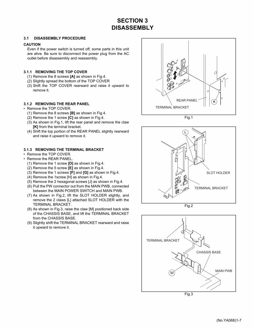
SECTION 3DISASSEMBLY
3.1 DISASSEMBLY PROCEDURECAUTION
Even if the power switch is turned off, some parts in this unitare alive. Be sure to disconnect the power plug from the ACoutlet before disassembly and reassembly.
3.1.1 REMOVING THE TOP COVER(1) Remove the 8 screws [A] as shown in Fig.4.(2) Slightly spread the bottom of the TOP COVER(3) Shift the TOP COVER rearward and raise it upward to
remove it.
3.1.2 REMOVING THE REAR PANEL• Remove the TOP COVER.
(1) Remove the 8 screws [B] as shown in Fig.4.(2) Remove the 1 screw [C] as shown in Fig.4.(3) As shown in Fig.1, lift the rear panel and remove the claw
[K] from the terminal bracket.(4) Shift the top portion of the REAR PANEL slightly rearward
and raise it upward to remove it.
3.1.3 REMOVING THE TERMINAL BRACKET• Remove the TOP COVER.• Remove the REAR PANEL.
(1) Remove the 1 screw [D] as shown in Fig.4.(2) Remove the 5 screw [E] as shown in Fig.4.(3) Remove the 1 screws [F] and [G] as shown in Fig.4.(4) Remove the 1screw [H] as shown in Fig.4.(5) Remove the 2 hexagonal screws [J] as shown in Fig.4.(6) Pull the PW connector out from the MAIN PWB, connected
between the MAIN POWER SWITCH and MAIN PWB.(7) As shown in Fig.2, lift the SLOT HOLDER slightly, and
remove the 2 claws [L] attached SLOT HOLDER with theTERMINAL BRACKET.
(8) As shown in Fig.3, raise the claw [M] positioned back sideof the CHASSIS BASE, and lift the TERMINAL BRACKETfrom the CHASSIS BASE.
(9) Slightly shift the TERMINAL BRACKET rearward and raiseit upward to remove it.
Fig.1
Fig.2
Fig.3
KREAR PANEL
TERMINAL BRACKET
TERMINAL BRACKET
SLOT HOLDER
L
TERMINAL BRACKET
CHASSIS BASE
MAIN PWBM

1-8 (No.YA068)
Fig.4
MAIN POWERSWITCH
AC INLET
EARTHWIRE
PWCONNECTOR
CRT SOCKET
PWB
CRT
LANDING
COIL
FRONT PANEL
SUBDEF.PWB
SPEAKER
DEG. COIL
FBT
FRONT
CONTROL
PWB
SIGNAL PWB
SLOT PWB
SLOT HOLDER
CHASSIS BASE
TERMINAL
BRACKET
EARTH WIRE
TOP COVER
BOTTOM COVER
MAIN POWERSWITCH
POWER
CORD
REAR PANEL
AC INLET
MAIN PWB
A
A
A
F
J
G
H
R
P N
D
B
C
EFig.3
( x 4)
( x 4)
( x 4)
( x 2)
( x 2)
( x 2)
( x 2)
( x 1)
( x 1)
( x 8)
( x 5)
( x 1)
( x 1) ( x 1)
Fig.1
Fig.2

(No.YA068)1-9
3.1.4 REMOVING THE SLOT HOLDER AND SLOT PWB• Remove the TOP COVER.• Remove the REAR PANEL.• Remove the TERMINAL BRACKET.
(1) Detach the connector connected SLOT PWB and SIGNALPWB, then remove the SLOT PWB with SLOT HOLDER.
(2) Remove the 4 screws [R] as shown in Fig.4.(3) Then remove the SLOT PWB from SLOT HOLDER.
3.1.5 REMOVING THE CHASSIS BASE• Remove the TOP COVER.• Remove the REAR PANEL.• Remove the TERMINAL BRACKET.
(1) Fall the unit down side ways as able to see the bottom side.(2) Lift the back side of the CHASSIS BASE slightly, and
separate it from BOTTOM COVER.(3) Raise the 2 claws positioned bottom of the CHASSIS
BASE, and detach the CHASSIS BASE from BOTTOMCOVER.
(4) Then pull the CHASSIS BASE out to rearward.
3.1.6 REMOVING THE BOTTOM COVER• Remove the TOP COVER.• Remove the REAR PANEL.• Remove the TERMINAL BRACKET.• Remove the CHASSIS BASE.
(1) Set the CRT front surface downward, and stand the bottomcover to facing it toward you.At this time, care must be exercised not to damage the frontpanel and CRT surface.
(2) Remove the 4 screws [N] as shown in Fig.4.(3) Remove the 2 screws [P] as shown in Fig.4.(4) While spreading the BOTTOM COVER to the bottom side,
pull it out to rearward to remove it.
3.1.7 REMOVING THE SPEAKER• Remove the TOP COVER.
(1) Slightly spread the claws of the speaker holder.(2) Pull up the SPEAKER to remove it.
3.1.8 CHECKING THE PW BOARDTo check the PW board from back side.
(1) As shown in Fig.5, place the unit for service.(2) Erect the chassis base vertically so that you can easily
check the PW board from back side.
Fig.5
CAUTION• Before turning on power, make sure that the earth wire
properly connected to the TERMINAL BRACKET, which isattached the main power switch and AC inlet. (Fig.6)
• And make sure that the CRT earth wire and the otherconnectors are properly connected.
• When erecting the CHASSIS BASE, be careful so that therewill be no contacting with the other PW board.
• Be careful while erecting the PW board, because easily falldown.
Fig.6
3.1.9 WIRE CLAMPING AND CABLE TYING(1) Be sure to clamp the wire.(2) Never remove the cable tie used for tying the wires
together.Should it be inadvertently removed, be sure to tie the wireswith a new cable tie.
MAIN PWBSIGNAL
PWB
TERMINAL
BRACKET
INSULATOR
(Card Board etc.)
STAND
Example of placement for SERVICE
TO MAIN PWB
( E2 )
AC INLET
TERMINAL
BRACKET
PLUG
EARTH WIRE
LUG
EARTH PLUG
POWER SW. CORE
FILTER

1-10 (No.YA068)
3.2 MEMORY IC REPLACEMENT3.2.1 MEMORY ICThis model uses memory IC. In the memory IC, there arememorized data for correctly operating for the video-chroma,deflection and the other control circuits. When replacing memory IC, be sure to use the IC written with theinitial values of data.
3.2.2 MEMORY IC REPLACEMENT PROCEDURE1. Power off
Turn the power off and unplug the power plug from the ACoutlet.
2. Replace ICBe sure to use the memory IC written with the initial settingdata.
3. Power onConnect the power plug into the AC outlet and turn the poweron.
4. Check and set SET-UP MENU items(1) Press the [MENU] button and the [CHROMA /PHASE]
button simultaneously.(2) The < SET-UP MENU > screen (Fig. 1) will be displayed.(3) Check the setting value of the each item of the < SET-UP
MENU >. If value is different, select it and set the correctvalue.
(4) Press the [MENU] button, and return to the normalscreen.
5. Check and set MENU itemsPress the [MENU] button and check the setting value of theeach item. If the value is different, select the item and set thecorrect value.
6. Adjust the front control itemsAdjust the CHROMA, PHASE, CONTRAST and BRIGHT.Not all items can be adjusted as expected if the signal has notbeen input correctly in the adjustments.
7. Confirm the items of SERVICE MENUConfirm the each item of the SERVICE MENU. Refer to thecorresponding page to operate the SERVICE MENU.
<SET-UP MENU>
Fig.1
< SET-UP MENU >
EXIT
CURSORPoint out the current adjusting item. Operate with the
[CHROMA/PHASE] and [CONTRAST/BRIGHT] button.
SETTING ITEMThe items of <SET-UPMENU>.
SETTING VALUE
FUNCTION DISPLAYWhen you move the cursor to select the item, the
function display changes the selected item.
OPERATION BUTTONIn the SERVICE MENU, the original button operation by
the front panel replaced with the displayed function.
Adjust each item of <SET-UP MENU> with the
[VOLUME/SELECT (+/-)].
PICTURE SUB ADJ.
H.POSITION : 00
V.POSITION : 00
WHITE BALANCE
CONTROL LOCK : OFF
STATUS DISPLAY : ON
REMOTE SYSTEM : MAKE
INPUT REMOTE : A-D
1
2 3
4
5
< BLOCK SELECT >
SIGNAL BLOCK
WHITE BALANCE BLOCK
DEFLECTION BLOCK
CONTROL BLOCK
SIG W/B DEF CTRL EXIT
<SERVICE MENU>
<D
®
@
®
~ ' ' ' ' ' ' ' ' '
DODOO

(No.YA068)1-11
3.2.3 FACTORY SETTING VALUE (USER MODE) INTIAL SETTING VALUE OF THE SET-UP MENU
INTIAL SETTING VALUE OF THE MENU
INTIAL SETTING VALUE OF FRONT PANEL CONTROLS
Setting item Setting content / Range Initial setting value
PICTURE SUB ADJ.
CONTRAST -10 ~ 00 ~ +10 00BRIGHT -10 ~ 00 ~ +10 00
CHROMA -10 ~ 00 ~ +10 00PHASE (NTSC) -10 ~ 00 ~ +10 00
H. POSITION -05 ~ +05 00V. POSITION -05 ~ +05 00
WHITE BALANCECUTOFF (R / G / B) -20 ~ +20 00
DRIVE (R / B) -20 ~ +20 00
CONTROL LOCK OFF
STATUS DISPLAY ON
REMOTE SYSTEM MAKE
INPUT REMOTE A-D
ON OFF
ON OFF
MAKE TRG.
A-D A/B
Setting item Setting content / Range Initial setting valueAPERTURE 00 ~ +40 00
ADJ. BAR POSI LOWER
COLOR TEMP 6500
COLOR SYSTEM AUTO
RUSH DELA STD.
LOWER UPPER
9300 6500
AUTO NTSC AUTO PAL
STD. SLOW
Control item(Front panel) Initial setting value
INPUT SELECT A
ASPECT OFF
BLUE CHECK OFF
COLOR OFF OFF
UNDER SCAN OFF
MENU OFF
VOLUME 20
CONTRAST 00
BRIGHT 00
CHROMA 00
PHASE NTSC : 00 PAL : NO EFFECT
r - i
r - i
r - i
r - i
r - i
r - i
r - - - i
r - i
I

1-12 (No.YA068)
3.2.4 SERVICE MENU SETTING ITEMS (SERVICE MODE)SIGNAL BLOCK
WHITE BALANCE BLOCK
DEFLECTION BLOCK
CONTROL BLOCK (Don't change the values, because all fixed)
3.2.5 LANDING MENU SETTING ITEMS
Item ContentsS01 BRIGHT
S02 CONTRAST
S03 CHROMA(PAL)
S04 CHROMA(NTSC)
S05 PHASE(NTSC)
S06 CHROMA
S07 BRIGHT
S08 CONTRAST
S09 BRIGHT
S10 CONTRAST
S11 PHASE(PAL)
S12 PHASE
S13 CONT TRACKING
Item Contents
W01 R CUTOFF
W02 G CUTOFF
W03 B CUTOFF
W04 R DRIVE (6500K)
W05 B DRIVE (6500K)
W06 R DRIVE (9300K)
W07 B DRIVE (9300K)
W08 R CUTOFF
W09 G CUTOFF
W10 B CUTOFF
W11 R DRIVE (6500K)
W12 B DRIVE (6500K)
W13 R DRIVE (9300K)
W14 B DRIVE (9300K)
W15 R CUTOFF
W16 G CUTOFF
W17 B CUTOFF
W18 R DRIVE (6500K)
W19 B DRIVE (6500K)
W20 R DRIVE (9300K)
W21 B DRIVE (9300K)
W22 R CUTOFF
W23 G CUTOFF
W24 B CUTOFF
Item Aspect ratio Scan size
Verticalfrequency Contents
D01
4:3NORMAL
SCAN50Hz
HORIZONTAL POSITION
D02 HORIZONTAL SIZE
D03 VERTICAL POSITION
D04 VERTICAL SIZE
D05 VERTICAL LINEARITY
D06 VERTICAL S-CORRECTION
D07 SIDEPIN PARABOLA
D08 SIDEPIN CORNER
There are many mode of the DEFLECTION BLOCK except for aboveDA1~DA8 (4:3 / 60Hz)DB1~DB8 (16:9 / 50Hz)DC1~DC8 (16:9 / 60Hz)DD1~DD8 (UNDER SCAN / 50Hz)DE1~DE8 (UNDER SCAN / 60Hz)DF7~DF8 (16:9 UNDER SCAN / 50Hz)
Item Contents
C01 DESTINATION
C02 BRIGHT POINT UPPER
C03 LOWER
C04 CONTRAST POINT UPPER
C05 LOWER
C06 CHROMA POINT UPPER
C07 LOWER
C08 PHASE POINT UPPER
C09 LOWER
C10 OSD HORIZONTAL POSITION
C11 OSD VERTICAL FREQUENCY 50Hz
C12 OSD VERTICAL FREQUENCY 60Hz
C13 HORIZONTAL CENTER (RGB)
C14 HORIZONTAL CENTER (COMPONENT)
C15 BRIGHT SERVICE
C16 SHARPNESS CENTER
C17 HVT H
C18 HVT V
C19 HVT H (UNDER SCAN)
C20 HVT V (UNDER SCAN)
C21 V-S.CORRECTION
C22 TRAPEZOID
C23 HOUR METER
C24 RUSH DELAY
C25 DEGAUSS DELAY TIME
C26~C33 SLOT IDENTIFY
C34 LANDING ENABLE
C35 LANDING START
Item Input signal Contents- - - PAL / NTSC LANDING

(No.YA068)1-13
3.3 REPLACEMENT OF CHIP COMPONENT3.3.1 CAUTIONS
(1) Avoid heating for more than 3 seconds. (2) Do not rub the electrodes and the resist parts of the pattern.(3) When removing a chip part, melt the solder adequately. (4) Do not reuse a chip part after removing it.
3.3.2 SOLDERING IRON(1) Use a high insulation soldering iron with a thin pointed end of it. (2) A 30w soldering iron is recommended for easily removing parts.
3.3.3 REPLACEMENT STEPS 1. How to remove Chip parts
[Resistors, capacitors, etc.]
(1) As shown in the figure, push the part with tweezers andalternately melt the solder at each end.
(2) Shift with the tweezers and remove the chip part.
[Transistors, diodes, variable resistors, etc.]
(1) Apply extra solder to each lead.
(2) As shown in the figure, push the part with tweezers andalternately melt the solder at each lead. Shift and removethe chip part.
NOTE :After removing the part, remove remaining solder from thepattern.
2. How to install Chip parts
[Resistors, capacitors, etc.]
(1) Apply solder to the pattern as indicated in the figure.
(2) Grasp the chip part with tweezers and place it on thesolder. Then heat and melt the solder at both ends of thechip part.
[Transistors, diodes, variable resistors, etc.]
(1) Apply solder to the pattern as indicated in the figure. (2) Grasp the chip part with tweezers and place it on the
solder. (3) First solder lead A as indicated in the figure.
(4) Then solder leads B and C.
SOLDER SOLDER
A
B
C
A
B
C

1-14 (No.YA068)
SECTION 4ADJUSTMENT
4.1 ADJUSTMENT PREPARATION(1) There are 2 ways of adjusting this unit: One is with the
MENU as On-Screen-Display and the other is theconventional method using adjustment parts andcomponents.
(2) The adjustment using the On-Screen-Display is madeon the basis of the initial setting values. The settingvalues which adjust the screen to the optimumcondition can be different from the initial settingvalues.
(3) Make sure that connection is correctly made AC to ACpower source.
(4) Turn on the power of the TV and measuring instruments forwarning up for at least 30 minutes before startingadjustments.
(5) If the receive or input signal is not specified, use the mostappropriate signal for adjustment.
(6) Never touch the parts (such as variable resistors,transformers and condensers) not shown in the adjustmentitems of this service adjustment.
(7) Unless otherwise specified in the adjustment items, presetthe values that the < SET-UP MENU >, MENU and FRONTPANEL CONTROL to initial conditions.
4.2 MEASURING INSTRUMENT(1) DC voltmeter (digital voltmeter)(2) HV voltmeter(3) Oscilloscope(4) Color temperature meter or Color analyser(5) Signal generator (PAL/NTSC)
4.3 PRESETTING FOR ADJUSTMENT
4.4 ADJUSTMENT ITEMSCHECK ITEM
HIGH VOLTAGE check HIGH VOLTAGE HOLD DOWN check
B1 VOLTAGEFOCUS ADJUSTMENTVIDEO CIRCUIT
WHITE BALANCE adjustment SUB BRIGHT adjustment SUB CONTRAST adjustment PAL CHROMA adjustment NTSC 3.58 CHROMA adjustment NTSC 3.58 PHASE adjustment COMPONENT CHROMA adjustment RGB BRIGHT adjustment RGB CONTRAST adjustment
DEFLECTION CIRCUIT H. POSITION / H. SIZE adjustment 4:3 SIDE PINCUSHION adjustment V. POSITION adjustment V. LIN. / V.S-CORRECTION adjustment 4:3 V. SIZE adjustment 16:9 V. SIZE adjustment 16:9 SIDE PINCUSHION adjustment UNDERSCAN H. POSITION / H. SIZE adjustment UNDERSCAN SIDE PINCUSHION adjustment 16:9 UNDERSCAN SIDE PINCUSHION adjustment
4.5 STANDARD SIGNALS FOR ADJUSTMENT ITEMS
APERTURE
ADJ. BAR POSITION
COLOR TEMP.
COLOR SYSTEM
RUSH DELAY
INPUT SELECT
ASPECT
BLUE CHECK
COLOR OFF
UNDERSCAN
MENU
VOLUME
CONTRAST
BRIGHT
CHROMA
PHASE (NTSC)
Setting item
00
LOWER
6500
AUTO
STD.
A
OFF (4 : 3)
OFF
OFF
OFF
OFF
20
00
00
00
00
Setting value
0.525V B-W
0% SETUP
COMPOSITE VIDEO SIGNAL (PAL/NTSC colour bar)
75% Saturation
BURST
PAL :0.3V(P-P)
NTSC:0.286V(P-P)
r------
J

(No.YA068)1-15
4.6 ADJUSTMENT LOCATIONS / WIRING DIAGRAM
D C B A
A
SLOT VIDEOPOWER SW
A
S
U
HV
S11pin :NC2pin :NC3pin :X-RAY24pin :X-RAY1
6pin :NC
1
6
CN1001
ASPECT COLOR OFF
BLUECHECK
UNDERSCAN
MENU +(UP) (DOWN)VOLUME/SELECT
CONTRAST /BRIGHT
CHROMA /PHASE
FRONT
FRONT
FRONT CONTROL PWB
CN1005CN1006
CN1002
SIGNAL PWB
DEG COIL
VR1901
TP-B1DEG
SLOT PWB
SPEAKER
CN1004
CN1003
PW
F1901 T5AH 250V
MAIN POWER SWITCH
CRT SOCKET PWB
B1 ADJ
DEF YOKE
CN2004
CN2003
TP-E
E2
UPPER
MIDDLE
LOWER
: FOCUS1
: FOCUS2
: SCREEN
SUB DEF. PWB
SUB DEF. PWB
FRONT
MAIN PWB
5pin :TP-E(GND )
COMPONENT/RGB INPUT CARD
(OPTION)
FBT
0 0 0 [QI O O O O [QI [QI [QI [QI [QI
WWWWWWWW I I I I ~----- ~ ~ I I I I
D~;;;;;;;:
=--------' D D
t
D
l
'
l.~
~
<'---->
@
t
t
t
.-----1 ---,
@

1-16 (No.YA068)
T
S3 R
CN6002 CN6001
IC6702
MEMORY IC
IC6701
MICRO
COMPUTER
CN6005
T
TP-47G
TP-47B
E1
CN8006 (50pin)
CN8005
TP-E
( )
SIGNAL PWB FRONTTOP
TOP
TOP
SLOT PWBCRT SOCKET PWB (SOLDER SIDE)
U
MAIN PWB
LANDING COIL
(canceller)
CRT EARTH WIRE
(BRAIDED ASS'Y)
COMPONENT/RGB INPUT CARD
(OPTION)
t
t l ---- !'[SJ
D
---~
D
D

(No.YA068)1-17
4.7 BASIC OPERATION OF SERVICE MENU4.7.1 SERVICE MENU ITEMSWith the SERVICE MENU, various settings can be made, andthey are broadly classified in the following items of adjustments.• It is no requirement for adjustment portion of the
DEFLECTION BLOCK and CONTROL BLOCK
4.7.2 HOW TO ENTER THE SERVICE MENU(1) Press [MENU] and [VOLUME/SELECT (+)] button
simultaneously (Fig. 1).The letter “S” appears at the upper left of the screen (Fig. 2).
(2) While displaying the letter "S", press [MENU] and[CHROMA /PHASE] button simultaneously (Fig.1).The screen display "PLEASE, DON'T TOUCH" (Fig. 3).
(3) While displaying the letters, press [VOLUME/SELECT (+ / -)]button to display the SERVICE MENU as shown in Fig. 4.
(4) Press the [MENU] button, then return to the normal screen.• If displaying the letters steps or state continues for more than
5 seconds without a further operation, the display extinguishesand the mode is released.
4.7.3 LANDING CORRECTION PROCEDURELanding correction is used only when uneven coloring isconspicuous.• Input the white signal
(1) Press [MENU] and [CONTRAST/BRIGHT] button simultaneously(Fig. 5). < LANDING > is displayed on the screen (Fig. 6).
(2) Adjust to the state where irregular color is not mostconspicuous with [VOLUME/SELECT(+ / -)] buttons (fig.5).
(3) If adjustment is completed, return with [MENU] button (Fig.5).
SIGNAL BLOCK This block adjusts the data of thevarious signal circuit controls.
WHITE BALANCE BLOCK This block adjusts the data of theWHITE BALANCE adjustment.
DEFLECTION BLOCK This block adjusts the data of theDEFLECTION circuit.
CONTROL BLOCK(Don't adjust)
This block adjusts the whole of thesystems.
Fig.5
Fig.6
(1) (3)
(2)
Item Setting value
LANDING :
(1)
(2)
(3)
Fig.1
Fig.2
Fig.3
Fig.4
S
PLEASE, DON'T TOUCH!
< BLOCK SELECT >
SIGNAL BLOCKWHITE BALANCE BLOCKDEFLECTION BLOCKCONTROL BLOCK
SETTING
ITEM
FUNCTION
DISPLAY
SIG W/B DEF CTRL EXIT
~ CHROMA CONTRAST( VOLUME/SELECT MENU
@= rn GAm D· ,,;,, PHASE BRIGHT ~
-1 ld-ld1-
0 CHROMA CONTRASTO VOlUME/SELECT MENU
@ : CD G-"'CD D· Oil> PHASE BHIGHT ~ I I 11 1-[=l--.-
. . : : - ~ : . . ' . ,_ ---------------------_,
,.l., **
1-18 (No.YA068)
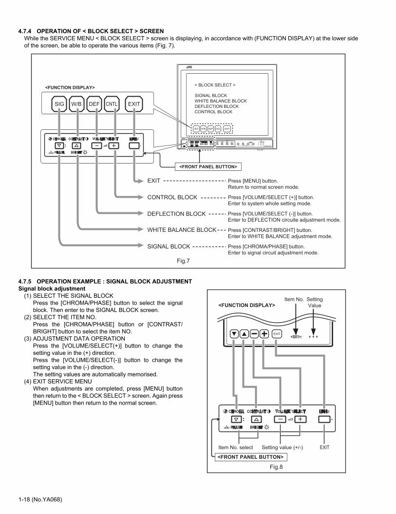
4.7.4 OPERATION OF < BLOCK SELECT > SCREENWhile the SERVICE MENU < BLOCK SELECT > screen is displaying, in accordance with (FUNCTION DISPLAY) at the lower sideof the screen, be able to operate the various items (Fig. 7).
4.7.5 OPERATION EXAMPLE : SIGNAL BLOCK ADJUSTMENTSignal block adjustment
(1) SELECT THE SIGNAL BLOCKPress the [CHROMA/PHASE] button to select the signalblock. Then enter to the SIGNAL BLOCK screen.
(2) SELECT THE ITEM NO.Press the [CHROMA/PHASE] button or [CONTRAST/BRIGHT] button to select the item NO.
(3) ADJUSTMENT DATA OPERATIONPress the [VOLUME/SELECT(+)] button to change thesetting value in the (+) direction.Press the [VOLUME/SELECT(-)] button to change thesetting value in the (-) direction.The setting values are automatically memorised.
(4) EXIT SERVICE MENUWhen adjustments are completed, press [MENU] buttonthen return to the < BLOCK SELECT > screen. Again press[MENU] button then return to the normal screen.
Fig.7
SIG W/B DEF CNTL EXIT
< BLOCK SELECT >
SIGNAL BLOCK
WHITE BALANCE BLOCK
DEFLECTION BLOCK
CONTROL BLOCK
SIG W/B DEF CNTL EXIT
WHITE BALANCE BLOCK Press [CONTRAST/BRIGHT] button.
Enter to WHITE BALANCE adjustment mode.
SIGNAL BLOCK Press [CHROMA/PHASE] button.
Enter to signal circuit adjustment mode.
DEFLECTION BLOCK Press [VOLUME/SELECT (-)] button.
Enter to DEFLECTION circuite adjustment mode.
CONTROL BLOCK Press [VOLUME/SELECT (+)] button.
Enter to system whole setting mode.
EXIT Press [MENU] button.
Return to normal screen mode.
<FUNCTION DISPLAY>
<FRONT PANEL BUTTON>
Fig.8
EXIT<S01>:
EXIT
Item No. Setting
Value<FUNCTION DISPLAY>
Item No. select Setting value (+/-)
<FRONT PANEL BUTTON>
JVC
~999~ ROMA CONTRASTO VOLUME/ SELECT MEN~
rn= rn G..dm D· HA~G~ __ --c
--------
:00000: , _______________ ,
l(!)(!)8(±)0 = = = ---r,;====~
* * *
~ CHROMA CONTRASTO VOLUME/ SELECT MENU
rn= rn G.dm D · oi>, PHASE BRIGHT~

(No.YA068)1-19
4.7.6 SERVICE MENU ITEMS SIGNAL BLOCK
WHITE BALANCE BLOCK
<S01> : EXIT DISP
SIGNAL BLOCKItem No. Setting value
Item No.
select buttonExit button
Display on/off button
Setting value
(+/-) button
DISPEXIT <S01>:
Fig.9
< FUNCTION DISPLAY >
<FRONT PANEL BUTTON>
< FUNCTION DISPLAY >
< FRONT PANEL BUTTON >
Exit button
Select the W01~W07 item adjust mode
Select the 9300 DRIVE mode
Select the 6500 DRIVE mode
Select the CUTOFF mode
EXITCUTO 65-D 93-D W01
< ITEM SELECT >
CUTOFF :CUTO
6500 DRIVE :65-D
9300 DRIVE :93-D
WHITE BALANCE BLOCK
Fig.10
W01 EXIT65-D 93-DCUTO
0 CHROMA CONTRASTO VOWME/SELECT
[D : C!J G""CD BRIGHTil
,---------------~
UNDER SCAN
D
I l.,_ ____________ ---t--, I ..__,......_,,...,_.....,_ I I__ _...J
0 CHROMA CONTRASTO VOWME/ SELECT
[D: C!J G""CD D · t:U:IP E BAI HT-J:l
~---------------, 1~~81±) DD ... I L--------------~
:00000~ _________ ...J

1-20 (No.YA068)
[ WHITE BALANCE ADJUSTMENT : METHOD 1 ]• Accordance with the screen display, select the each WHITE BALANCE mode following below.• Refer to the "Low-Light adjustment" corresponding page about detailed adjustment steps.
CUTOFF ADJUSTMENT MODE (LOW LIGHT ADJUSTMENT)
DRIVE ADJUSTMENT MODE (HIGH LIGHT)• Refer to the "High-Light adjustment" corresponding page about detailed adjustment steps.
[WHITE BALANCE ADJUSTMENT : METHOD 2]
R CUTOFF :
< FUNCTION DISPLAY >
< FRONT PANEL BUTTON >
Contents Setting value
RGB EXITSERV
Contents button
Display 1H line button
Setting value (+/-) button
Exit button
CUTOFF ADJUSTMENT MODE
RGB EXITSERV R CUTOFF :
Fig.11
R
G
B
6500 R DRIVE :
< FUNCTION DISPLAY >
< FRONT PANEL BUTTON >
Contents button
Display 1H line button
Setting value (+/-) button
Exit button
RGB EXITSERV
DRIVE ADJUSTMENT MODE
RGB EXITSERV 6500 R DRIVE :
Fig.12
ContentsColor temp. Setting value
6500
9300
R
B
< FUNCTION DISPLAY >
<FRONT PANEL BUTTON>
<W01> :
W01~W07 ITEM ADJUSTMENT MODE
DISPEXIT <W01 > :
Fig.13
Item No. Setting value
EXIT DISP
Item No.
select buttonExit button
Display on/off button
Setting value
(+/-) button
r----------------lOCB±) o *** : L----------------
0 CHROMA CONTRASTO VOWME/SELECT
u:J: C!l G ""CD ..,. PHASE BAIGHT il
MENU
D · r----------------(X..l=l±) o *** : L----------------
0CHROMA CONTRASTO VOWME/SELECT MENU
u:J: C!l G""CD BRIGHTil
D· ~---------------, : ~~E)!±) DD ... I ---------------~

(No.YA068)1-21
DEFLECTION BLOCK
CONTROL BLOCK
< FUNCTION DISPLAY >
<FRONT PANEL BUTTON>
<D01> :
DEFLECTION BLOCK
EXIT <D01 > :
Item No. Setting value
Fig.14
EXIT
Item No.
select buttonExit buttonSetting value
(+/-) button
< FUNCTION DISPLAY >
<FRONT PANEL BUTTON>
<C01> :
CONTROL BLOCK
EXIT <C01 > :
Item No. Setting value
Fig.15
EXIT
Item No.
select buttonExit buttonSetting value
(+/-) button
II' CHROMA CONTRAST ct VOWME/SELECT MENU
[!], CD G""CD BRIGHTn
D · ~---------------, l~~Ell±l D ... I L--------------~
------------------~
l!'CHROMA CONTRAST(t VOWME/SELECT MENU
[!], CD G""CD D· BRIGHTn
~---------------, l~~Ell±l D ... I L--------------~

1-22 (No.YA068)
4.7.7 SERVICE MENU FLOW CHART
< BLOCK SELECT >
SIGNAL BLOCKWHITE BALANCE BLOCKDEFLECTION BLOCKCONTROL BLOCK
SIG W/B DEF CTRL EXIT
EXITRGB SERV
R CUTOFF :
EXITR-B DISP
6500 R DRIVE :
DISPEXIT <W01>:
DISPEXIT <S01>:
EXITCUTO 65-D 93-D W01
< ITEM SELECT >
CUTOFF :CUTO
6500 DRIVE :65-D
9300 DRIVE :93-D
EXIT <D01>:
EXIT <C01>:
SERVICE MENU
LANDING CORRECTION
<BLOCK SELECT> SCREEN
SIGNAL BLOCK
CUTOFF ADJUSTMENT
DRIVE ADJUSTMENT
W01 ~ W24 ADJUSTMENTDEFLECTION BLOCK
CONTROL BLOCK
WHITE BALANCE BLOCKMENU SCREEN
(2)
(3) (1)
(1)
LANDING :
0 CHROMA CONTRAST() VOLUME/ SELECT MENU
Cil= CIJ G-"'CD D· ~r BRIGHT(f bd bd1-DODOO
'8CHROMA CONTRAST() VOLUME/ SELECT MENU
Cil= CIJ G-"'CD D · tU:I PHASE BRIGHT~ I I ,_
~~8(±)00 ...
008(±)0
-**
DODOO 008(±)0
~~81±100
~~8(±)0 ...

(No.YA068)1-23
4.8 INITIAL SETTING VALUE OF SERVICE MENUIt is no requirement for adjustment of the part of the tables. Don' t change the values.
[SIGNAL BLOCK]
[WHITE BALANCE BLOCK]
Item Input signal Contents Variable range Initial valueS01
VIDEO
BRIGHT 000 ~ 255 137
S02 CONTRAST 000 ~ 127 059
S03 CHROMA(PAL) 000 ~ 127 064
S04 CHROMA(NTSC) 000 ~ 127 062
S05 PHASE(NTSC) 000 ~ 127 060
S06 COMPONENT CHROMA 000 ~ 127 080
S07RGB
BRIGHT 000 ~ 127 076
S08 CONTRAST -128 ~ 000 ~ +127 -001
S09
VIDEO
UNDER SCAN BRIGHT -128 ~ 000 ~ +127 000
S10 UNDER SCAN CONTRAST -128 ~ 000 ~ +127 -009
S11 PHASE(PAL) 000 ~ 127 062(FIXED)
S12 COMPONENT PHASE 000 ~ 127 063(FIXED)
S13 VIDEO CONT TRACKING 000 ~ 031 016(FIXED)
Item Input signal Contents Variable range Initial valueW01
VIDEO
R CUTOFF 000 ~ 255 050
W02 G CUTOFF 000 ~ 255 050
W03 B CUTOFF 000 ~ 255 050
W04 R DRIVE (6500) 000 ~ 127 062
W05 B DRIVE (6500) 000 ~ 127 048
W06 R DRIVE (9300) 000 ~ 127 078
W07 B DRIVE (9300) 000 ~ 127 066
W08
COMPONENT
R CUTOFF -128 ~ 000 ~ +127 000
W09 G CUTOFF -128 ~ 000 ~ +127 000
W10 B CUTOFF -128 ~ 000 ~ +127 000
W11 R DRIVE (6500) -128 ~ 000 ~ +127 000
W12 B DRIVE (9300) -128 ~ 000 ~ +127 000
W13 R DRIVE (6500) -128 ~ 000 ~ +127 000
W14 B DRIVE (9300) -128 ~ 000 ~ +127 000
W15
RGB
R CUTOFF -128 ~ 000 ~ +127 000
W16 G CUTOFF -128 ~ 000 ~ +127 000
W17 B CUTOFF -128 ~ 000 ~ +127 000
W18 R DRIVE (6500) -128 ~ 000 ~ +127 000
W19 B DRIVE (9300) -128 ~ 000 ~ +127 000
W20 R DRIVE (6500) -128 ~ 000 ~ +127 000
W21 B DRIVE (9300) -128 ~ 000 ~ +127 000
W22
VIDEO
UNDER SCAN R CUTOFF -128 ~ 000 ~ +127 000
W23 UNDER SCAN G CUTOFF -128 ~ 000 ~ +127 000
W24 UNDER SCAN B CUTOFF -128 ~ 000 ~ +127 000
-

1-24 (No.YA068)
[DEFLECTION BLOCK]
Item Aspect ratio/ Scan size
Vertical frequency Contents Variable range Initial value
D01
4:3NORMAL 50Hz
HORIZONTAL POSITION 000 ~ 031 012D02 HORIZONTAL SIZE 000 ~ 063 040D03 VERTICAL POSITION 000 ~ 127 041D04 VERTICAL SIZE 000 ~ 127 058D05 VERTICAL LINEARITY 000 ~ 031 025D06 VERTICAL S-CORRECTION 000 ~ 063 040D07 SIDEPIN PARABOLA 000 ~ 063 030D08 SIDEPIN CORNER 000 ~ 031 018DA1
4:3NORMAL 60Hz
HORIZONTAL POSITION -032 ~ 000 ~ +031 +002DA2 HORIZONTAL SIZE -064 ~ 000 ~ +063 -4DA3 VERTICAL POSITION -128 ~ 000 ~ +127 +002DA4 VERTICAL SIZE -128 ~ 000 ~ +127 000DA5 VERTICAL LINEARITY -032 ~ 000 ~ +031 -1DA6 VERTICAL S-CORRECTION -064 ~ 000 ~ +063 000DA7 SIDEPIN PARABOLA -064 ~ 000 ~ +063 +001DA8 SIDEPIN CORNER -032 ~ 000 ~ +031 +001DB1
16:9NORMAL 50Hz
HORIZONTAL POSITION -032 ~ 000 ~ +031 000DB2 HORIZONTAL SIZE -064 ~ 000 ~ +063 000DB3 VERTICAL POSITION -128 ~ 000 ~ +127 000DB4 VERTICAL SIZE -128 ~ 000 ~ +127 -28DB5 VERTICAL LINEARITY -032 ~ 000 ~ +031 000DB6 VERTICAL S-CORRECTION -064 ~ 000 ~ +063 000DB7 SIDEPIN PARABOLA -064 ~ 000 ~ +063 -11DB8 SIDEPIN CORNER -032 ~ 000 ~ +031 000DC1
16:9NORMAL 60Hz
HORIZONTAL POSITION -032 ~ 000 ~ +031 000DC2 HORIZONTAL SIZE -064 ~ 000 ~ +063 000DC3 VERTICAL POSITION -128 ~ 000 ~ +127 000DC4 VERTICAL SIZE -128 ~ 000 ~ +127 -27DC5 VERTICAL LINEARITY -032 ~ 000 ~ +031 000DC6 VERTICAL S-CORRECTION -064 ~ 000 ~ +063 -1DC7 SIDEPIN PARABOLA -064 ~ 000 ~ +063 -12DC8 SIDEPIN CORNER -032 ~ 000 ~ +031 -1DD1
4:3UNDERSCAN
50Hz
HORIZONTAL POSITION -032 ~ 000 ~ +031 000DD2 HORIZONTAL SIZE -064 ~ 000 ~ +063 -7DD3 VERTICAL POSITION -128 ~ 000 ~ +127 000DD4 VERTICAL SIZE -128 ~ 000 ~ +127 -3DD5 VERTICAL LINEARITY -032 ~ 000 ~ +031 000DD6 VERTICAL S-CORRECTION -064 ~ 000 ~ +063 000DD7 SIDEPIN PARABOLA -064 ~ 000 ~ +063 -19DD8 SIDEPIN CORNER -032 ~ 000 ~ +031 -1DE1
4:3UNDERSCAN
60Hz
HORIZONTAL POSITION -032 ~ 000 ~ +031 000DE2 HORIZONTAL SIZE -064 ~ 000 ~ +063 -6DE3 VERTICAL POSITION -128 ~ 000 ~ +127 000DE4 VERTICAL SIZE -128 ~ 000 ~ +127 -2DE5 VERTICAL LINEARITY -032 ~ 000 ~ +031 000DE6 VERTICAL S-CORRECTION -064 ~ 000 ~ +063 000DE7 SIDEPIN PARABOLA -064 ~ 000 ~ +063 -20DE8 SIDEPIN CORNER -032 ~ 000 ~ +031 -2DF7 16:9
UNDER SCAN50Hz
SIDEPIN PARABOLA -064 ~ 000 ~ +063 +007DF8 SIDEPIN CORNER -032 ~ 000 ~ +031 000DG7 16:9
UNDER SCAN60Hz
SIDEPIN PARABOLA -064 ~ 000 ~ +063 +008DG8 SIDEPIN CORNER -032 ~ 000 ~ +031 +001

(No.YA068)1-25
[CONTROL BLOCK]
4.9 INITIAL SETTING VALUE OF LANDING MENU
Item. Contents Variable range Initial valueC01 DESTINATION 000 ~ 129 001(US/EU)
C02BRIGHT POINT
UPPER 000 ~ 255 016
C03 LOWER 000 ~ 255 026
C04CONTRAST POINT
UPPER 000 ~ 127 016
C05 LOWER 000 ~ 127 026
C06CHROMA POINT
UPPER 000 ~ 127 040
C07 LOWER 000 ~ 127 040
C08PHASE POINT
UPPER 000 ~ 127 040
C09 LOWER 000 ~ 127 040
C10 OSD HORIZONTAL POSITION 000 ~ 010 000
C11 OSD VERTICAL FREQUENCY 50Hz 000 ~ 010 004
C12 OSD VERTICAL FREQUENCY 60Hz 000 ~ 010 002
C13 HORIZONTAL CENTER (RGB) -128 ~ 000 ~ +127 +007
C14 HORIZONTAL CENTER (COMPONENT) -128 ~ 000 ~ +127 +002
C15 BRIGHT SERVICE 000 ~ 127 000
C16 SHARPNESS CENTER 000 ~ 127 028
C17 HVT H 000 ~ 007 007
C18 HVT V 000 ~ 007 003
C19 HVT H (UNDER SCAN) 000 ~ 007 004
C20 HVT V (UNDER SCAN) 000 ~ 007 002
C21 V-SS.CR 000 ~ 015 005
C22 TRAPEZOID 000 ~ 127 068
C23 HOUR METER 001 ~ 650 001
C24 RUSH DELAY 000 ~ 255 032
C25 DEGAUSS DELAY TIME 000 ~ 255 011
C26 SLOT IDENTIFY 000 ~ 255 000
C27 SLOT IDENTIFY 000 ~ 255 066
C28 SLOT IDENTIFY 000 ~ 255 000
C29 SLOT IDENTIFY 000 ~ 255 001
C30 SLOT IDENTIFY 000 ~ 255 000
C31 SLOT IDENTIFY 000 ~ 255 000
C32 SLOT IDENTIFY 000 ~ 255 000
C33 SLOT IDENTIFY 000 ~ 255 000
C34 LANDING ENABLE 000/001 000
C35 LANDING START 000/001 000
Item Contents Variable range Initial value- - - LANDING CORRECTION -08 ~ 00 ~ +08 00

1-26 (No.YA068)
4.10 ADJUSTMENT PROCEDURE4.10.1 CHECK ITEM
Item Measuring instrument Test points Adjustment part Description
HIGHVOLTAGEcheck
HV voltmeter CRT anode SCREEN VR[in FBT]
(1) Receive a whole black signal.(2) Connect the HV voltmeter to the CRT anode and
check it as 25.0kV±1.3kV.
HIGHVOLTAGEHOLD DOWNcheck
HV voltmeter Resistor(57.7kΩ, ±289Ω)
S1 3-pin: X-RAY1S1 4-pin: X-RAY2[SUB DEF.PWB]
• After repairing the high voltage hold down circuit, thiscircuit shall be checked to operate correctly.(1) Receive a whole black signal.(2) Turn the power switch on.(3) Refer to the figure, connect the resistor between S1
connector 3-pin and 4-pin.(4) Make sure that the screen picture disappears.(5) Disconnect the power plug.(6) Remove the resistor.(7) Again connect the power plug.(8) Turn the power switch to on.(9) Make sure that the normal picture is displayed on the
screen.
CONNECTOR
NCNCNC
FBT
57.7k 289
3 2 156 4
RESISTER
S1
Q ± Q
D

(No.YA068)1-27
4.10.2 B1 VOLTAGE
4.10.3 FOCUS
Item Measuring instrument Test points Adjustment part Description
B1 VOLTAGE Signal generator
DC voltmeter
TP-B1
TP-E(GND)(E2)
[MAIN PWB]
B1 ADJ VR(VR1901)[MAIN PWB]
SCREEN VR[in FBT]
(1) Receive a whole black signal.(2) Connect a DC voltmeter to TP-B1 and TP-E( ).(3) Adjust the B1 ADJ VR(VR1901) so that B1 voltage is
at 53V±0.2V.(4) If B1 voltage is out of range, adjust it with B1 ADJ
VR(VR1901).
Item Measuring instrument Test points Adjustment part Description
FOCUS Signal generator
FOCUS 1 VRFOCUS 2 VR[In FBT]
(1) Input the crosshatch pattern signal.(2) Adjust the FOCUS 1 VR (Vertical line) and FOCUS
2 VR (Horizontal line) for optimum focus where moi-re is not apparent.
(3) Darken the picture and adjust the focus by turningcounter-clockwise from the position where focus ispoor.
(4) Alternately repeat the above steps to obtain theoptimum position.
.J,

1-28 (No.YA068)
4.10.4 VIDEO CIRCUITWhen you perform WHITE BALANCE adjustment, be sure to input a video composite signal. Moreover, set the aspect ratio to 4:3. Itis no requirement to adjust in 16:9 mode.
Item Measuring instrument Test points Adjustment part Description
WHITE BALANCE LOW LIGHT
Signal generator
SCREEN VR[in FBT] [WHITE BALANCEBLOCK]W01 : R CUTOFFW02 : G CUTOFFW03 : B CUTOFF
• After checking that the voltage of B1 power supplyvoltage is right.(1) Input the gray scale signal.(2) Select the WHITE BALANCE BLOCK with
[CONTRAST/BRIGHT] button (< W/B >) from <BLOCK SELECT > SERVICE MENU screen.
(3) Select the < W01 >~< W07 > adjust modewith[VOLUME/SELECT + (UP)] button (< W01 >).
(4) Confirm the initial setting value of < W01 >(RCUTOFF), < W02 >(G CUTOFF) and < W03 >(BCUTOFF) are 50 as shown below.
(5) Exit the < W01 >~< W07 > adjust mode with [MENU]button (< EXIT >).
(6) Select the CUTOFF adjustment mode with[CHROMA/PHASE] button (< CUTO >) from <WHITE BALANCE BLOCK > screen.
(7) Display the single horizontal line with [CONTRAST/BRIGHT] button (< SERV >). Carefully adjust theSCREEN VR to horizontal line appears faintly, not toshine much.
(8) Gradually turn the SCREEN VR from the left to theright direction to bring one of the red, green and bluecolors faintly visible.
(9) Then select R, G or B color with [CHROMA/PHASE]button (< RGB >) that color except for appears first,and adjusting 2 colors CUTOFF values, and makesingle horizontal line visible white.
(10) Readjust the SCREEN VR to appear the singlehorizontal line faintly.
(11) Cancel the single horizontal line with [CONTRAST/PHASE] button (< SERV >).
(12) Exit the WHITE BALANCE BLOCK with [MENU]button (< EXIT >).
Item Initial setting value
<W01> R CUTOFF
<W02> G CUTOFF
<W03> B CUTOFF
50
50
50
WHITE BALANCE BLOCK
EXITCUTO 65-D 93-D W01
CUTOFF :CUTO6500 DRIVE :65-D9300 DRIVE :93-D
EXITDISP <W0#>:
Setting value indicatedSERVICE NUMBER
indicated
W01~W07 ITEM ADJUST MODE
CUTOFF ADJUSTMENT MODE
EXITRGB SERV
R CUTOFF :
Select 6500 DRIVE adjustment mode
Select CUTOFF adjustment mode
Select 9300 DRIVE adjustment mode
Select W01~W07 item adjustment mode
Adjustment mode exit
Select SERVICE NUMBER
Data operate (+/ )
Display single horizontal line switch
Adjustment mode exit

(No.YA068)1-29
6500K WHITEBALANCEHIGH LIGHT
Signal generator
Coloranalyser (Color temperature meter)
[WHITE BALANCE BLOCK]W04 : R DRIVEW05 : B DRIVE
• Check the LOW LIGHT adjustment has been finishedcorrectly before performing HIGH LIGHT adjustment.(1) Input the gray scale signal.(2) Select the WHITE BALANCE BLOCK mode with
[CONTRAST/BRIGHT] button (< W/B >) from <BLOCKSELECT > SERVICE MENU screen.
(3) Select the < W01 >~< W07 > adjust mode with[VOLUME/SELECT +] button (< W01 >).
(4) Apply the sensor of the color analyser to the CRTsurface, portion of the 100% white.
(5) Adjust the < W04 > (R DRIVE) or < W05 > (BDRIVE) to setting 6500K (X=0.313, Y=0.329) bypressing [CHROMA/PHASE] button (< R-B >)alternately.
(6) Exit the WHITE BALANCE BLOCK with [MENU]button (< EXIT >).
9300K WHITEBALANCEHIGH LIGHT
Signal generator
Coloranalyser (Color temperature meter)
[WHITE BALANCE BLOCK]W06 : R DRIVEW07 : B DRIVE
• Check the LOW LIGHT adjustment has been finishedcorrectly before performing HIGH LIGHT adjustment.(1) Input the gray scale signal.(2) Select the WHITE BALANCE BLOCK mode with
[CONTRAST/BRIGHT] button (< W/B >) from <BLOCK SELECT > SERVICE MENU screen.
(3) Select the < W01 >~< W07 > adjust mode with[VOLUME/SELECT +] button (< W01 >).
(4) Apply the sensor of the color analyser to the CRTsurface, portion of the 100% white.
(5) Adjust the < 9300 R DRIVE > or < 9300 B DRIVE >to setting 9300K (X=0.283, Y=0.297) by pressing[CHROMA/PHASE] button (< R-B >) alternately.
(6) Exit the WHITE BALANCE BLOCK with [MENU]button (< EXIT >).
Item Measuring instrument Test points Adjustment part Description

1-30 (No.YA068)
BRIGHT Signal generator
[SIGNAL BLOCK]S01 : BRIGHT
• Under the condition that LOW LIGHT adjustment hasbeen correctly finished.(1) Input the gray scale signal.(2) Select the SIGNAL BLOCK with [CHROMA /
PHASE] button (< SIG >) from < BLOCK SELECT >screen.
(3) Select < S01 >(BRIGHT).(4) Adjust the < S01 > to where the 0% black part
component faintly brightens.(5) Check the BRIGHT adjustment by alternately turning
the screen display in WHITE BALANCE BLOCK <CUTOFF > mode.
(6) Check the LOW LIGHT adjustment has beenfinished correctly before performing HIGH LIGHTadjustment.
CONTRAST Signalgenerator
Oscilloscope
TP-47GTP-E[CRT SOCKETPWB]
[SIGNAL BLOCK]S02 : CONTRAST
(1) Input the full color bar signal (75% white)(2) Connect the oscilloscope to TP-47G and TP-E.(3) Select the SIGNAL BLOCK with [CHROMA /
PHASE] button (< SIG >) from < BLOCK SELECT >screen.
(4) Select the < S02 >(CONTRAST).(5) Adjust the < S02 > to become the voltage different
between 75% white and 0% black to 34V±2V asshown in figure.
Item Measuring instrument Test points Adjustment part Description
75%
WHITE W Y Cy G
Mg R B BL
V75-BL=34V 2V
_J '
±
- ----_____ _!_

(No.YA068)1-31
Item Measuring instrument Test points Adjustment part Adjustment procedure
PAL CHROMA Signagenerator
Oscilloscope
TP-47BTP-E[CRT SOCKETPWB]
[SIGNAL BLOCK]S03 : PAL CHROMA
(1) Input the PAL color bar signal (75% white).(2) Connect the oscilloscope to TP-47B and TP-E.(3) Select the SIGNAL BLOCK with [CHROMA/PHASE]
button (< SIG >) from < BLOCK SELECT > screen.(4) Select the < S03 >(PAL CHROMA).(5) Adjust the < S03 > to become the voltage different
between 75% white and blue to 0V±2V as shown infigure.
NTSC CHROMA Signalgenerator
Oscilloscope
TP-47BTP-E[CRT SOCKETPWB]
[SIGNAL BLOCK]S04: NTSC CHROMA
(1) Input the NTSC full color bar signal (75% white).(2) Connect the oscilloscope to TP-47B and TP-E.(3) Select the SIGNAL BLOCK with [CHROMA/PHASE]
button (< SIG >) from < BLOCK SELECT > screen.(4) Select the < S04 >(NTSC CHROMA).(5) Adjust the < S04 > to become the voltage different
between 75% white and blue to 0V±2V as shown infigure.
75% W
Y
Cy
G
Mg
R
B
0V 2V
75% W
Y
Cy
G
Mg
R
B
0V 2V
-
- -- -f--+
---=------------Li_
....r,_
--
-
~ - -- -f--- ± ______________ Ll_

1-32 (No.YA068)
NTSC PHASE Signalgenerator
Oscilloscope
TP-47BTP-E[CRT SOCKETPWB]
[SIGNAL BLOCK]S05: NTSC PHASE
(1) Input the NTSC color bar signal (75% white).(2) Connect the oscilloscope to TP-47B and TP-E.(3) Select the SIGNAL BLOCK with [CHROMA/PHASE]
button (< SIG >) from < BLOCK SELECT > screen.(4) Select the < S05 >(NTSC PHASE).(5) Adjust the < S05 > to become the voltage different
between white and magenta to 0V±2V as shown infigure.
Item Measuring instrument Test points Adjustment part Adjustment procedure
75% W
Y
Cy
G
Mg
R
B
0V 2V
The following 3 items (COMPONENT SIGNAL CHROMA, RGB SIGNAL BRIGHT, RGB SIGNAL CONTRAST) are performed whenhaving equipped with the OPTION CARD (IF-C01COMG). When the Component / RGB input card (IF-C01COMG) is inserted to therear slot, turn off the main power switch on the rear panel.
Item Measuring instrument Test points Adjustment part Adjustment procedure
COMPONENTCHROMA
Component /RGB inputcard(IF-C01COMG)
Signalgenerator
Oscilloscope
TP-47BTP-E[CRT SOCKETPWB]
[SIGNAL BLOCK]S06:COMPONENT CHROMA
(1) Input the COMPONENT color bar signal (100/0/100/0 interface) to the each terminal of the Component /RGB input card.
(2) In case of using the composite sync. signal, input thesync. signal to the HD/Cs terminal only. But in caseof using the separate sync. signal, input the horizon-tal sync. signal to the HD/Cs terminal and verticalsync. signal to the VD terminal.
(3) Select the INPUT SELECT < SLOT D >.(4) Connect the oscilloscope to TP-47B and TP-E.(5) Select the SIGNAL BLOCK.(6) Select the < S06 > (COMPONENT CHROMA).(7) Adjust the < S06 > to become the voltage different
between 75% white and blue to 0V±2V as shown infigure.
75% W
Y
Cy
G
Mg
R
B
0V 2V
--
------- -r--~ ±
______________ ___..!__
-
--r--
±
---=-------------_l__

(No.YA068)1-33
RGB BRIGHT Component / RGB input card(IF-C01COMG)
Signalgenerator
[SIGNAL BLOCK]S07 : RGB BRIGHT
(1) Input the whole black signal to the each terminal ofthe Component / RGB input card.
(2) In case of using the composite sync. signal, input thesync. signal to the HD/Cs terminal only. But in caseof using the separate sync. signal, input thehorizontal sync. signal to the HD/Cs terminal andvertical sync. signal to the VD terminal.
(3) Select the INPUT SELECT < SLOT D >.(4) Select the SIGNAL BLOCK.(5) Select the < S07 >(RGB BRIGHT).(6) Adjust the < S07 > to where the sprit color bar 0%
black component faintly brightens.(7) Check it out by pressing the [DISP] button on and off.
RGBCONTRAST
Component / RGB input card(IF-C01COMG)
Signalgenerator
Oscilloscope
TP-47GTP-E[CRT SOCKETPWB]
[SIGNAL BLOCK]S08 : RGB CONTRAST
(1) Input the RGB color bar signal (75% white) to theeach terminal of the Component / RGB input card.
(2) In case of using the composite sync. signal, input thesync. signal to the HD/Cs terminal only. But in caseof using the separate sync. signal, input the horizon-tal sync. signal to the HD/Cs terminal and verticalsync. signal to the VD terminal.
(3) Select the INPUT SELECT < SLOT D >.(4) Connect the oscilloscope to TP-47G and TP-E.(5) Select the SIGNAL BLOCK.(6) Select the < S08 >(RGB CONTRAST).(7) Adjust the < S08 > to become the voltage different
between 75% white and blue to 34V±2V as shown infigure.
Item Measuring instrument Test points Adjustment part Adjustment procedure
75%
WHITE W Y Cy G
Mg R B BL
V75-BL=(34 2)V
~ -
-
r ±
---- - ______ !_

1-34 (No.YA068)
4.10.5 DEFLECTION CIRCUITThere are 2 kind of adjustment for the DEFLECTION circuit, PAL and NTSC. The adjustment using PAL signal is as the standard ofall DEFLECTION adjustment. The "#" mark in the table given below expresses the number of each adjustment item. The screen aspectratio 4 : 3 at 50Hz (PAL) is regarded as the reference value for all adjustments. The other values obtained in the adjustments usingother signals become the offset values as opposed to the reference values.Therefore, the adjustments must always be carried out in order of PAL and NTSC. When it does not adjust in this turn, and whenoperation which is different by the middle is carried out, it is necessary to readjust from the beginning.
ModeDisplay
Aspect ratio Scan size Vertical frequency
4:3 NORMAL SCAN50Hz(PAL) D0#
60Hz(NTSC) DA#
16:9 NORMAL SCAN50Hz(PAL) DB#
60Hz(NTSC) DC#
4:3 UNDER SCAN50Hz(PAL) DD#
60Hz(NTSC) DE#
16:9 UNDER SCAN50Hz(PAL) DF7, DF8
60Hz(NTSC) DG7, DG8
Although the procedure is described about the adjustment at the time of inputting a PAL signal into below, please perform adjustmentwhich inputs an NTSC signal continuously.However, about each adjustment item of "Vertical center", "Vertical linearity", "16:9 Vertical size" and "Horizontal size and center atthe time of under scan mode", it considers as the adjustment only to a PAL signal, and adjustment with an NTSC signal is notrequired.
Item Measuring instrument Test points Adjustment part Adjustment procedure
H. POSITION / H. SIZE
Signal generator
[DEFLECTION BLOCK]D01 : H. CENTERD02 : H. SIZE
(1) Input the PAL crosshatch signal.(2) Select DEFLECTION BLOCK with [VOLUME /SE-
LECT - ] button (< DEF >) from < BLOCK SELECT >SERVICE MENU screen.
(3) Adjust < D01 >(H.CENTER) to align the picture cen-ter with the CRT center.
(4) Adjust < D02 >(H. SIZE) to set horizontal size to95%.
(5) Repeat above step 4 and 5 to adjust correctly.
4:3 SIDEPINCUSHION
Signal generator
[DEFLECTION BLOCK]D07 : SIDEPIN PARABOLAD08 : SIDEPIN CORNER
(1) Input the PAL crosshatch signal.(2) Confirm the side pincushion of the four corners in the
screen.(3) If not optimum, adjust < D07 >(SIDEPIN PARABOLA)
and < D08 >(SIDEPIN CORNER) to become correct-ly.
Picture size 100%
Screen size 95%
--~ ·---------------------------------------~
I·-------------------------------------------~
(No.YA068)1-35
V. POSITION Signal generator
[DEFLECTION BLOCK]D03 : V. POSITION
(1) Input the PAL circle pattern signal.(2) Adjust < D03 >(V. POSITION) to agree with CRT
center and signal center of vertical direction.
V. LINEARITY /V. S-CORRECTION
Signal generator
[DEFLECTION BLOCK]D04 : V.SIZED05 : V.LIND06 : V. S-COR
(1) Input the PAL circle pattern signal.(2) Confirm < D04 >(V. SIZE) about 100% for linearity
adjustment.(3) Adjust < D05 >(V. LIN) to become correctly about
vertical size and vertical linearity.(4) Adjust < D06 >(V. S-COR) that circle pattern
becomes the true circle at top and bottom of thescreen.
Item Measuring instrument Test points Adjustment part Adjustment procedure
<V. LINEARITY>
<V. S-CORRECTION>
Correct adjustment
Correct adjustment
Vertical extension Horizontal extension
Top extension Bottom extension

1-36 (No.YA068)
4:3 V. SIZE
Signal generator
[DEFLECTION BLOCK]D04 : V.SIZE
(1) Input the PAL crosshatch signal.(2) Adjust < D04 >(V. SIZE) to become the vertical scan
size to 95%.
16:9 V. SIZE
Signal generator
[DEFLECTION BLOCK]DB04 : V. SIZE
(1) Input the PAL circle pattern signal.(2) Select the aspect ratio to the 16:9 mode.(3) Adjust < DB04 >(V. SIZE) to the vertical size become
the value given below.
16:9SIDEPINCUSHION
Signal generator
[DEFLECTION BLOCK]DB07 : SIDEPIN PARABOLADB08 : SIDEPIN CORNER
(1) Input the PAL crosshatch signal (2) Select the aspect ratio to the 16:9 mode.(3) Confirm the side pincushion of the four corners in the
screen.(4) If not optimum, adjust < DB07 >(SIDEPIN
PARABOLA) and < DB08 >(SIDEPIN CORNER) tobecome correctly.
Item Measuring instrument Test points Adjustment part Adjustment procedure
Picture size
100%
Screen size
95%
Vertical size 171mm 3mm
171mm 3mm
·-----------------------------------____________ J
I __ LI ±
T ±

(No.YA068)1-37
UNDERSCANH. POSITION / H. SIZE
Signal generator
[DEFLECTION BLOCK]DD1 : H. CENTERDD2 : H. SIZE
(1) Input the PAL circle pattern signal.(2) Select the aspect ratio to the 4:3 mode.(3) Select the underscan mode to ON.(4) Adjust the < DD1 >(H. CENTER) to the left and right
blanking width become equal.(5) Adjust the < DD2 >(H. SIZE) to the left and right
blanking widths become the value given below.
4:3UNDERSCANSIDE PINCUSHION
Signal generator
[DEFLECTION BLOCK]DD7 :SIDEPIN PARABOLADD8 :SIDEPIN CORNER
(1) Input the PAL crosshatch signal.(2) Select the aspect not to the 4:3 mode.(3) Select the underscan mode to ON.(4) Confirm the side pincushion of the four corners in the
screen.(5) If not optimum, adjust < DD7 >(SIDEPIN
PARABOLA) and < DD8 >(SIDEPIN CORNER) tobecome correctly.
(6) If the warps are happened by adjust the sidepincushion, readjust the above-mentioned < DD1 >and < DD2 >.
16:9UNDERSCANSIDE PINCUSHION
Signal generator
[DEFLECTION BLOCK]DD7 :SIDEPIN PARABOLADD8 :SIDEPIN CORNER
(1) Input the PAL crosshatch signal.(2) Select the aspect ratio to the 16:9 mode.(3) Select the underscan mode to ON.(4) Confirm the side pincushion of the four corners in the
screen.(5) If not optimum, adjust < DF7 >(SIDEPIN
PARABOLA) and < DF8 >(SIDEPIN CORNER) tobecome correctly.
(6) If the warps are happened by adjust the sidepincushion, readjust the above-mentioned < DD1 >and < DD2 >.
Item Measuring instrument Test points Adjustment part Adjustment procedure
Horizontal
Blanking Width
(one side of screen)6mm 9mm
6mm 9mm6mm 9mm
Picture size
Effective
screen size
(rr ~-. I +- I
-I
~ U) .. I+ .. I+
- -

1-38 (No.YA068)
SECTION 5TROUBLE SHOOTING
5.1 OUTLINEThis model includes a SELF DIAGNOSIS FUNCTION that checks the circuit operating status and in event of malfunction, displaysand stores the data in a memory. The data are stored in memory.Fault detection starts with the I2C bus and is performed according to the input states of the control lines connected to the MAIN CPU.
5.2 USAGE5.2.1 SELF DIAGNOSIS FUNCTION MODE ENTRY
(1) While press the [MENU] button and [CONTRAST/BRIGHT]button simultaneously, and push the POWER switch to turnon.
(2) Then displays the SELF-DIAGNOSIS FUNCTION screen. Make sure all items of this MENU are "O" (Fig.1).
(3) If "X" is in items (Fig.2), press the [MENU] button and[VOLUME /SELECT - (DOWN)] button at same time.
5.2.2 CONTENTS
• If in event malfunction at RASTER not display, at this timePOWER LED flashes.
5.2.3 SELF DIAGNOSIS FUNCTION MODE RELEASETurn the POWER switch off or disconnect the power plug fromAC outlet. In this way, not to clear the error counts.
5.2.4 RESET THE ERROR COUNT(1) While press the [MENU] button and [CHROMA/PHASE]
button simultaneously, and push the MAIN POWER switchon.
(2) Then displays the screen as shown in Fig.3. Press the [ + ]key. Then clear the error count of the each item.
5.2.5 FAULT HISTORYThe fault history counts up to a maximum of 9 times for eachitem. If the number of times exceeds 9, the display remains at 9.The fault history remains stored in the memory until deleted.
Check item
Detected contents
Detection method Cause
B1
The over-current of B1 line is checked and vertical oscillation is checked.
It will be detect the B1-PRO port in IC6701 51-pin on SIGNAL PWB.
Destruction of a level oscillation transistor Q1521 on MAIN PWB can be considered.Vertical oscillationDestruction of a vertical out IC1401 on MAIN PWB can be considered.
X-RAY
The unusual rise of CRT anode voltage is checked.
IC6701 50-pin on SIGNAL PWB
Destruction of a resonance capacitor (C2521, C2522, C2528) on SUB DEF PWB or FBT T1551 on MAIN PWB can be considered.
Cause Led flashing cycleX-RAY PROTECTION Quickly (0.1 sec on / 0.1 sec off cycles)
B1 OVER CURRENT PROTECTION Slowly (1.0 sec on / 1.0 sec off cycles)
PROTECTOR
B1 :
X-RAY :
Fig.1
Fig.2
PROTECTOR
B1
1
:
X-RAY :
SELF DIAGNOSIS RESET
<SET-UP MENU> RESETAre you sure?
"Yes" then <+>"No" then <MENU>
Fig.3
0
0
+ 0
X

No.YA068 2-1
5.NOTE FOR REPAIRING SERVICEThis model's power circuit is partly different in the GND. Thedifference of the GND is shown by the LIVE : ( ) side GND and theISOLATED(NEUTRAL) : ( ) side GND. Therefore, care must betaken for the following points.
(1)Do not touch the LIVE side GND or the LIVE side GND and the ISOLATED(NEUTRAL) side GND simultaneously. if the above caution is not respected, an electric shock may be caused. Therefore, make sure that the power cord is surely removed from the receptacle when, for example, the chassis is pulled out.
(2)Do not short between the LIVE side GND and ISOLATED(NEUTRAL) side GND or never measure with a measuring apparatus measure with a measuring apparatus ( oscilloscope, etc.) the LIVE side GND and ISOLATED(NEUTRAL) side GND at the same time. If the above precaution is not respected, a fuse or any parts will be broken.
Since the circuit diagram is a standard one, the circuit andcircuit constants may be subject to change for improvementwithout any notice.
NOTEDue improvement in performance, some part numbers showin the circuit diagram may not agree with those indicated inthe part list.When ordering parts, please use the numbers that appearin the Parts List.
STANDARD CIRCUIT DIAGRAMNOTE ON USING CIRCUIT DIAGRAMS
(7)Ground symbol
: LIVE side ground
: ISOLATED(NEUTRAL) side ground
: EARTH ground
: DIGITAL ground
(6)Connecting method
: Connector : Wrapping or soldering
: Receptacle
(5)Test point
: Test point : Only test point display
Respective voltage values are indicated
: B1
: 9V : 5V
: B2 (12V)
(4)Power Supply
Type
MM : Metalized mylar capacitorPP : Polypropylene capacitorMPP : Metalized polypropylene capacitorMF : Metalized film capacitorTF : Thin film capacitorBP : Bipolar electrolytic capacitorTAN : Tantalum capacitor
(3)Coils
No unit
Others
: [µH]
: As specified
No indication : Ceramic capacitor
(2)CapacitorsCapacitance value
1 or higher : [pF]less than 1 : [µF]Withstand voltageNo indication : DC50[V]
Others : DC withstand voltage [V]
AC indicated : AC withstand voltage [V]Electrolytic Capacitors
47/50[Example]: Capacitance value [µF]/withstand voltage[V]
Composition resistor 1/2 [W] is specified as 1/2S or Comp.
Type
No indication : Carbon resistorOMR : Oxide metal film resistorMFR : Metal film resistorMPR : Metal plate resistorUNFR : Uninflammable resistorFR : Fusible resistor
4.INDICATIONS ON THE CIRCUIT DIAGRAM(1)Resistors
Resistance value
No unit : [ ]
K : [ k ]M
Rated allowable powerNo indication : 1/16 [W]
Others : As specified
: [M ]
3.INDICATION OF PARTS SYMBOL [EXAMPLE]
In the PW board : R1209 R209
1.SAFETYThe components identified by the symbol and shading arecritical for safety. For continued safety replace safety ciriticalcomponents only with manufactures recommended parts.
Since the voltage values of signal circuit vary to some extentaccording to adjustments, use them as reference values.
2.SPECIFIED VOLTAGE AND WAVEFORM VALUESThe voltage and waveform values have been measured under thefollowing conditions.
(1)Input signal : Colour bar signal
(2)Setting positions of each knob/button and variable resistor
(3)Internal resistance of tester : DC 20k /V
(4)Oscilloscope sweeping time : H 20µs / div
: V 5ms / div
: Othters Sweeping time isspecified
(5)Voltage values : All DC voltage values
: Original setting position when shipped
TM-H150CG/E, TM-H150CG/U
• •
g ----= •o•o nnnn =
* =
i *
D 0
• -+ --.>---.-
.l
• ,J,.
g ~ Q v g
• .l
•
*
• • •
• *

No.YA068
SEMICONDUCTOR SHAPES
CONTENTSSEMICONDUCTOR SHAPES ......................................................................2-2BLOCK DIAGRAM........................................................................................2-3CIRCUIT DIAGRAMS....................................................................................2-5
SIGNAL PWB CIRCUIT DIAGRAM ............................................................................................................ 2-5MAIN PWB CIRCUIT DIAGRAM ................................................................................................................ 2-9SUB DEF PWB CIRCUIT DIAGRAM ........................................................................................................ 2-13CRT SOCKET PWB CIRCUIT DIAGRAM ................................................................................................. 2-15FRONT CONTROL PWB CIRCUIT DIAGRAM.......................................................................................... 2-17SLOT PWB CIRCUIT DIAGRAM .............................................................................................................. 2-19
PATTERN DIAGRAMS .............................................................................. 2-21MAIN PWB PATTERN .............................................................................................................................. 2-21SIGNAL PWB PATTERN .......................................................................................................................... 2-23FRONT CONTROL PWB PATTERN ......................................................................................................... 2-25SLOT PWB PATTERN .............................................................................................................................. 2-25CRT SOCKET PWB PATTERN ................................................................................................................. 2-27SUB DEF PWB PATTERN ........................................................................................................................ 2-28
ICBOTTOM VIEW FRONT VIEW TOP VIEW
1 N
N1
OUT
E
ININ OUTE
1 N
TOP VIEW
N
1
N
N
N
1
N
CHIP IC
TRANSISTORBOTTOM VIEW FRONT VIEW TOP VIEW
CHIP TR
ECB
E C B
C
B EB(G)
E(S)
C(D) E C BE C B
2-2
G] ~ ; ~ ~ ~
GJ Q ~ ~ 101 -------+
.
0 D ~ .

No.YA068 No.YA068
VIDEO A
AUDIO A
IC6002VIDEO/AUDIO
SW
IC6101COMBFILTER
IC6102 VIDEO SW
IC6201PAL 1H DELAY
IC6602INT/SLOT SW
IC6601RGB/COMPONENT
SW
D1901RECT
T1901SW
TRANSF.
IC1973REG.
IC1905VOLTAGE
FEEDBACK
IC1901POWER
REG.
FOCUS
SCREEN
T1551HVT
B1EHV
(V)
(H)
DEF.YOKE
Q1521H.OUT
KEYFUNCTION
LED
Q1501H.DRIVE
IC6701
MICRO COMPUTERIC6702
MEMORY
RGBOUT
V01CRT
CRT SOCKET PWB
F1901AC
INLET
MAIN PWB
REMOTE
IC6501VIDEO
/RGB/DEFPROCESS
IC8001SYNCMIXER
SPEAKER
FRONTCONTROL
PWB
IC1601AUDIO OUT
SIGNAL PWB
9 V
VIDEO
AUDIO A
Y IN
C IN
Y OUT
C OUT
CPHD
G/Y,R/R-Y,B/B-Y
R/G/BAUDIO
SYNC
VERT.
HORI.
CS/HDVD
Y C
SCP
IC1401V.OUT
Q1932B1 PROT.
KEY
FBP
IC6803IC6801
TIMINGPULSE
GENERAT.
IC8002 SW
SLOTCONNECTOR
SLOT PWB
VIDEO B
IC6001I/O PORT
EXTENSION
IC6802
T1902SW
TRANSF.
D1920RECT
LF1901
7 V
IC1411DISTORTION CORRECT
AUDIO OUT
R/G/B
SYNC
AUDIO
SCL 2SDA 2
SCL 3SDA 3
SCL 3SDA 3
SCL 3SDA 3
SCL 1SDA 1
SCL 1SDA 1
SCL 1SDA 1
AUDIO OUT
KEY
R-YB-Y
R-YB-Y
YR-YB-Y
VIDEO A
VIDEO B
Y/C
AUDIO OUT
Q3301Q3302 Q3303
R-YB-Y
R/G/B
IN
OUT
IN
OUT
IN
OUT
IN
OUT
IN
OUTAUDIO B
AUDIO B
LF1902
Y/C
IC1971REG.
12 V
AUDIO A
VIDEO A
VIDEO B
Y
AUDIO B
C
TIMINGPULSE
GENERAT.
TIMINGPULSE
GENERAT.
1HDELAY
x0.5
CLOCK
Y
Y
PULSEGENE.
LINEARITYCORRECT V PHASE
CHROMADEMOD. TRAP
SYNCSEP
HOR.COUNTDOWN
VERT.COUNTDOWN VP OUT
HD OUT
HOR.PHASE SHIFT H DRIVE
SCP OUT
RGBOUT
RGBMATRIX
Y CLAMP
UV CLAMP R-YB-Y
Y
HORI.
VERT.
YR-YB-Y
Y
C
Y
G/Y,R/R-Y,B/B-Y
G/YR/R-YB/B-Y
R/G/B
BLOCK DIAGRAM
2-42-3
r---
-n
....- ·-::--- - -
-.-------, , ,......_ __ ----.--------------------------------------,-, I I :: : = - : " ~· · ----,.-+I._.!..-.-::_---:._-; • .-------: I I .-------l==~i--o_;~~---+--i-+-----1_~ __ ~_; __ -_-:_-~---~ _i~ _ __. ~----,~' !-,rp-ifi --.-~-s7"':--a:"'__;_ ... : I.-,:: _J I
---------- • J
1 lt!-----+w-------+-------
~ l~~ - ______..,______-l~----W--:ri 6Y: ~ t
~ ~-=------~ ~---+-,
-' : : : - :
' - -- ' ' - ' L------.J I I I -
I ~ _ _J
l 0 0 00
00 00
i ~, ___________ ____,
w L • ~ ~-w----::----
111-----------' ...._ ___ _ r I I I
- - - -J
*
... ....
-' 'l
..... - -I I ;----------
1 i [@] I • I I :
.---'-l -------,-~-;.-------· __________ I_·~ -,~ l&I I I
I I ------------
-------- ----- I ~___, , - - ---- - - - - - -
...________. ,_______, H I ,..__ _ ___,
* .--, I ,
I ~-------------------~
I I I I •

No.YA068 No.YA068
MODE DC (V)PIN NO.MODE DC (V)PIN NO.
MODE DC (V)PIN NO.MODE DC (V)PIN NO.
IC6001 1 0 2 0 3 4.9 4 4.9 5 4.8 6 4 7 4.8 8 0 9 4.9 10 4.9 11 4.9 12 4.9 13 2.1 14 1.5 15 4.8 16 4.9 IC6002 1 4.6 2 4.9 3 4.2 4 4.9 5 4.2 6 2.6 7 4.2 8 4.9 9 4.2 10 4.9 11 4.2 12 2.8 13 4.2 14 4.9 15 4.9 16 0 17 4.7 18 4.9 19 0 20 4.2 21 0 22 4.9 23 4.2 24 4.1 25 5 26 4.2 27 4.2 28 9 29 3.4 30 4.9 31 4.3 32 4.9 IC6003 1 5.4 2 2.1 3 2.1 4 0 5 0.8 6 10.7 7 10.7 8 11.9 IC6004 1 5.4 2 5.4 3 5.4 4 5.4 5 0 6 5.4 7 5.4 8 5.4 9 5.4 10 11.9 IC6101 1 4.8 2 1.3 3 3.1 4 2.1 5 1.8 6 4.9 7 0 8 4.9 9 4.7 10 4.8 11 0 12 0 13 2.4 14 2.1 15 4.9 16 0 17 2.4 18 3.1 19 1.7 20 2.1 IC6102 1 7.4 2 8.4 3 7.3 4 0 5 7.4 6 11.9 7 6.6 8 0 IC6201 1 4.3 2 4.5 3 4.4 4 4.2
5 8.9 6 1.2 7 0.6 8 4.2 9 4.2 10 2.2 11 2.3 12 0 13 2.4 14 4.9 15 2.4 16 3.5 17 1.5 18 1.5 19 3.4 20 10.4 21 0 22 4.4 23 4.4 24 8.2 25 8.2 26 5.1 27 5.2 28 4.3 29 4.5 30 4.5 IC6501 1 1.5 2 1.1 3 3.9 4 1.6 5 2.1 6 2.1 7 8.2 8 4 9 4 10 4 11 1.8 12 4.9 13 2.4 14 0 15 3 16 6.3 17 0.1 18 4.5 19 0 20 7.4 21 5.9 22 8.9 23 1.3 24 3.9 25 0.5 26 0 27 4.1 28 4.3 29 4.6 30 4.9 31 4.8 32 0 33 3.4 34 3.4 35 3.4 36 0 37 3.4 38 3.4 39 3.4 40 8.9 41 2.3 42 2.4 43 2.4 44 0 45 6 46 8.9 47 0 48 3.6 49 5.2 50 3.7 51 4.9 52 4.9 53 6.3 54 6.9 55 4.9 56 0 IC6601 1 0 2 0.4 3 0 4 3.3 5 0 6 11.9 7 0 8 0 9 0 10 0 11 0 12 0 13 0 14 3.3 15 2.9 16 11.9 IC6602 1 2.4 2 0 3 2.4 4 2.4
5 0 6 0 7 0 8 0 9 11.9 10 11.9 11 11.9 12 0.4 13 1.6 14 1.6 15 2.4 16 11.9 IC6903 1 8.8 2 0 3 4.9 Q6001 C 11.9 E 4.3 B 4.9 Q6002 C 11.9 E 4.3 B 4.8 Q6003 C 11.5 E 3.5 B 4.1 Q6101 C 11.8 E 4.3 B 5 Q6102 C 4.8 E 1.4 B 2.1 Q6103 C 7.3 E 1.5 B 2.1 Q6104 C 11.9 E 6.7 B 7.3 Q6105 C 6.9 E 2.6 B 3.3 Q6106 C 11.9 E 6.3 B 6.9 Q6201 C 6.4 E 1.5 B 2.4 Q6202 C 11.9 E 5.2 B 6.3 Q6203 C 7.6 E 2 B 2.2 Q6204 C 11.9 E 7 B 7.6 Q6107 C 11.9 E 4.4 B 5 Q6208 C 11.9 E 3.8 B 4.5 Q6211 C 11.9 E 3.8 B 4.5 Q6108 C 8.4 E 0 B 0 Q6206 C 9 E 2.8 B 3 Q6207 C 9 E 2.8 B 3.5 Q6512 C 5.2 E 0 B 1.1 Q6513 C 0.6 E 0 B 2.7 Q6205 C 11.9 E 2.9 B 2.2
Q6109 C 11.9 E 3.3 B 3.9 Q6401 C 8.9 E 0 B 0 Q6402 C 1.3 E 8.4 B 8.9 Q6502 C 0.6 E 0 B 0 Q6111 C 11.8 E 1 B 1.6 Q6216 C 11.8 E 1.5 B 2.2 Q6217 C 11.9 E 1.8 B 2.4 Q6501 C 0 E 0 B 4.2 Q6514 C 0.6 E 0 B 0 Q6515 C 8.9 E 5.1 B 0.6 Q6516 C 8.9 E 3.8 B 4.8 Q6601 C 11.9 E 2.9 B 3.5 Q6603 C 11.9 E 2.2 B 3.9 Q6605 C 11.9 E 3.3 B 3.9 Q6607 C 11.9 E 0 B 0 Q6609 C 11.9 E 0 B 0 Q6611 C 11.9 E 0 B 0 Q6612 C 11.9 E 0 B 0 Q6507 C 0 E 4.3 B 3.7 Q6503 C 0 E 3.1 B 2.4 Q6504 C 0 E 3.1 B 2.4 Q6505 C 0 E 3 B 2.3 Q6508 C 0 E 0 B 4.8 Q6509 C 11.9 E 0 B 0 Q6510 C 4.3 E 0 B 0 Q6511 C 0 E 0 B 0.6
!
!
SIGNAL PWB ASSY(1/2)
FX-6143A-H2
SLOT PWB
CRT SOCKET PWB
IC6904
C6055
C6054
D6034
IC6601
CN6005
IC6602
IC6102
R6129
Q6108
R6101
R6102
R6103
Q6101
FL6101
R6104
R6554
R6105
R6106
IC6101Q6102
C6103
C6115
C6101
C6104
C6106
L6101
R6109
R6201
C6601
C6113
C6111
C6112
L6102
C6118
R6111
C6116
K6002
R6112
Q6103
R6136
L6103
C6603
C6108
IC6003
C6604
C6110
L6104
C6117
R6113R6107
R6108
R6114
R6115
C6123
Q6104
R6118
R6119
FL6102
R6120
Q6105L6106
R6123
R6054
R6116
R6117
C6254
R6232
R6121
R6141
Q6106
R6124
C6122
R6122
Q6201
R6202
R6203
R6234
Q6202
R6206
R6207
FL6201
R6208
Q6203
R6210
C6131
R6204
R6205R6211
Q6204
R6212
C6201
R6209
D6018
R6009
R6643
R6019
R6020
R6144
R6606
C6128
C6125
R6127
R6128
Q6107
R6125
R6126
D6019
D6020
C6144
C6143
D6029
D6030
R6615
R6039
C6141
C6105
D6031
D6032
R6553
Q6512
R6043
R6533
R6534
C6530
R6131
R6132
R6130
Q6109
R6133
C6126
R6214
R6215
R6213
Q6205
R6216
C6205
C6114
Q6208
Q6211
R6237
R6249
R6241
R6250
R6134
R6231C6236
R6604
Q6603
Q6601
Q6605
C6038
L6201
Q6210
R6616
Q6209
R6240
R6614
R6619
R6620
R6236
C6237
R6235
Q6111
R6140
R6233
D6021
C6234
Q6216
R6256
C6235
C6525
C6526
Q6217
R6259
R6644
R6645
R6646
R6647
R6135
K6101
C6211
C6518
CN60S3
C6218
K6103
J6004
C6517
R6531
C6501
C6527
C6504
C6505
C6524
C6902
C6024
C6001
R6242
R6058
R6059
C6045
C6046
R6648
Q6612
C6040
R6532
C6202
Q6513
R6535
K6201
K6202
IC6901
C6903
Q6516
R6519
R6057
R6546
Q6501
R6510
C6238
R6522
R6247
J6003
J6002
R6514
R6511
R6513
R6512
R6248
IC6004
Y6101
R6063
Q6001
J6006
Q6607R6632
R6633
Y6102Q6609
CN600T
C6120 C6119
C6102
Q6611
R6634
C6121
C6258
C6259
Q6402
D6027
D6028
C6253
J6005
R6520
R6621
R6622
C6260
C6606
R6238
R6239
R6137
C6145
R6270
R6269
R6138
R6244
R6246
R6001
R6139
R6271
C6107
C6109
C6605
R6142 R6143
C6130
Q6110
R6002
R6003
R6004
R6064
R6006
R6007
R6008
C6030
R6051
R6052
R6053
CP6901
C6901
C6002
C6904
R6268
R6785
D6705
C6132
C6133
C6134 C6135
C6249
C6246
C6247 C6248
CN600R
C6136
C6252
C6034
C6035
C6137
Q6515
R6536
C6608
C6609
Q6514
C6611
C6613 C6615 C6617
C6256
C6138
C6257
C6139
C6250
R6537
R6110
K6003
R6055
R6056
C6533
C6532
C6531
C6210
C6033
C6142
C6036
C6037
C6039
C6243
C6534
R6066
R6068R6069
C6041
R6072R6073C6042 C6044
R6070
R6071
R6067
R6074
C6223
C6227
C6043
R6036
R6021
R6026
D6023
D6025
D6024
D6026
C6003
C6005
R6023
R6028
R6024
R6029
R6022
R6027
Q6002
R6025
R6030
C6004
C6007
R6031
R6033
R6034
R6032
Q6003
R6035
C6008
C6009
C6010
C6031 R6037
D6033
C6006
R6047
C6012
C6011
C6014
C6020
C6025
IC6002
C6017
C6013
C6028
C6016
C6027
C6019
C6021
C6022
C6023
C6032
C6026
R6050
R6049
C6029
C6015
R6048
D6022
J6001
D6001
D6002
D6003
D6004 D6006
D6010
D6011
D6012
D6013 D6015
D6007
D6016
D6008
D6017
IC6001
R6623
R6605
R6627
R6628
R6637
R6638R6629
R6639
R6603
R6608
C6602
R6607
R6612
R6613
R6624
C6607
IC6201
C6213
R6262
C6228
C6229
C6214
Q6207
Q6206
R6260
R6261
C6230
C6231
C6233
C6222
C6224
C6244
C6215
C6217
C6245
R6265
C6216
C6221
C6232
C6225
R6226
R6225
C6226
R6223
R6221
R6222
R6224
R6227
R6228
R6501
X6201
X6202
R6217
C6207
IC6501
C6523
C6206
R6502
R6503
C6503
R6504
R6505
X6503
C6516
C6508
C6509
C6510
C6511
C6512
C6513
C6514
C6519
C6521
C6522
C6241
C6240
C6129
C6529
C6506
C6127
C6515
R6508
C6502 R6517
R6516
R6515
R6509
C6212
C6209
R6218
C6242
C6208
D6502
D6501
R6530
Q6503
Q6504
Q6505
R6523
R6524 R6525
R6540R6541
D6505D6503
R6518
D6514D6513D6512
D6517
D6516D6515
R6547
R6548
R6549
Q6511
Q6510
R6545 R6544
R6550
D6508
D6509
D6510
D6520
Q6508
Q6509
R6542
R6528
R6543
D6518
D6506
D6507
D6511
R6529
Q6507
D6519
R6405
Q6401
C6401
D6504
R6401
D6401R6402
R6404
R6406
R6403
C6403
Q6502
R6521
R6506
R6507 C6507
SD
I
SC
L4
SD
A4
SC
L3
VB
LK
SD
A3
SLT
_AB
XR
AY
VP
RE
M
EN
AB
LE
SLO
T4
SLO
T3
SLO
T2
SLO
T1
SLO
T14
V
ST
B7V
BC
HK
OS
D_B
WB
PLS
SLT
_EN
OS
D_R
OS
D_G
RG
B
AB
L
FS
TB
LK
SC
L1
SD
A1
FB
PHD
VID
EO
CP
9V
HP
LS
B1P
RO
T
5VSC
P
R60
10R
6011
R60
12R
6013
R60
15R
6016
R60
17R
6018
R60
14
YC
_DE
T
12V
AU
DIO
AN78L05-T
/16
/16
CD4053BNS-X
QGB1505J1-25
CD4053BNS-X
NJM2234M-XE
CE42697-001 TC90A49AP
/50
CH
/16
/50
/50
QQL244K-100Z
/16
/16
/50
/50
QQL244K-100Z
/16
CE42681-001Y
/16QTNC1CM-476Z
/16
BA10358
/16QTNC1CM-476Z
/16
QQL244K-100Z
/50
CH
CE42697-001
QQL244K-330Z
CH
CE42697-001
MA3091/M/-X
/50
/16
/16
/16
/16
/50
/16
/50
/10
/10
/35
/35
CE42681-001Y
CH
/50
QGA2501F1-03
/16
NQR0357-002X
QMD2B04-001
/16
/16
/50
/50
/16
/50
/16
/16
/16
CH
CE42681-001Y
CE42681-001Y
BA17809T
/16
CEMB021-002
LA6515
CEMN036-005
QJB003-113011
/16 /16
/16
CEMB021-002
/50
CH
/50
CH
2SA965/OY/-T
/16
QMD2B04-001
/16
/16
N
/16QTNC1CM-476Z
N
/16QTNC1CM-476Z
/16
/50
CPICP-N10-Y
CP
/16
/16
/16
MA3051/M/-X
QGA2501F1-03
CH
NQR0357-002X
CH
/16
/16
/50
/50
1/2QRK126J-470X
/10
/10
/50
1%NRSA02F-750X
1%NRSA02F-750X
1%NRSA02F-750X
/50
/50
/16
/50
1%NRSA02F-750X
/16
/50
/50
/50
MA3091/M/-X
/16
/50
/10
/10
/50
/16
MM1311BD
/50
/50
/50
/10
/10
/50
/50
/25
/50
CH
/50
CH
CH
QNZ0561-001
JLC1562BF-X
/16
TA8772AN
/16
/16
/16
/16
/16
/16
/50
CH
/16
/16
/16
/16
/16
/16
/16
CH
CE40749-001Z
CE40668-001Z
TA1276AN
/16
/16
/50
CSB503F30
/16
/16
/16
/16
/16
/16
/16
/16
/16
/50
/16
/16
/16
/10
/50
/16
/10
/16
/16
/16
/16
CH/35
N
N
N
N
CH
CH
CH
CH
CH
N
CH
CH
.1
100
*3
10k
*4
1k
3.3k
1k
*1
1k
OPEN
10k
220
*1
.01
180p
100
.01
.01
100
0
100
.1
.01
.01
100
820
.01
0
*1
100
47
.1
47
.1
.01
1.5k100
100
1k
330
5p
*1
4.7k
1k
1k
*1
33
27k
OPEN
47k
OPEN
OPEN
390
1k
100
*1
10k
22p
2.2k
*1
1k
330
680
*1
4.7k
1k
1k
*1
8.2k
OPEN
OPEN
OPEN1k
*1
10k
OPEN
2.2k
1.5k
100
100
100
0
220
OPEN
10
OPEN
OPEN
*1
100
4.7k
OPEN
OPEN
.1
.1
*3
*3
1.5k
10k
10
.22
*3
*3
68k
*4
10k
10k
22k
0.0022
3.3k
1.8k
1k
*1
2.2k
OPEN
3.3k
1.5k
1k
*1
2.2k
OPEN
100
*1
*1
OPEN
OPEN
0
0
0
OPENOPEN
22k
*1
*1
*1
2.2
OPEN
OPEN
4.7k
OPEN
OPEN
1k
22k
12k
OPEN
OPEN
OPEN
*1
3.3k
OPEN
OPEN
1
*1
3.3k
1
47
47
*1
3.3k
100
100
100
100
1.2k
47p
.47
.1
100
100
100
2.2
10
470
22
100
100
100
0
OPEN
OPEN
OPEN
OPEN
10k
*4
OPEN
100
27p
*4
10k100
*1
1k
1k
220k
*4
4.7k
OPEN
4.7k
OPEN
0
0
OPEN
OPEN
OPEN
OPEN
0
*1
*1680
2.2k
OPEN*1
.1 100
.1
*1
1.5k
OPEN
47p
47p
*3
*3
.1
OPEN
0
1M
.1
OPEN
180k
180k
220
.1
OPEN
100
100
390
680
1.5k
OPEN
100
47
47
47
OPEN OPEN
OPEN
OPEN
1.5k
1.5k
1.5k
0
1.5k
1.5k
1.5k
.01
OPEN
OPEN
OPEN
.1
.1
.1
OPEN
100
OPEN
OPEN
OPEN OPEN
180p
OPEN
OPEN OPEN
180p
OPEN
180p
180p
180p
*1
8.2k
OPEN
OPEN
*4
OPEN
OPEN OPEN OPEN
OPEN
OPEN
OPEN
OPEN
OPEN
47k
6.8k
100
OPEN
OPEN
OPEN
OPEN
47p
180p
.1
OPEN
OPEN
OPEN
10
10
15k
10k1k
.01
12k10kOPEN OPEN
56
47
1k
0
.47
.47
33
75
75
75
*3
*3
*3
*3
4.7
4.7
47k
47k
33k
33k
470
470
*1
10k
10k
.1
4.7
75
47k
33k
470
*1
10k
.1
2.2
2.2
.01 470
.1
100k
.01
.47
.47
.01
.1
.01
.01
.01
.47
.47
.01
.01
.047
.01
150p
22
100
100
150p
150p
100
OPEN
*3
*3
*3
*3 *3
*3
*3
*3
*3 *3
*3
*3
*3
*3
0
10k
680
2.2k
680
2.2k1.5k
1.5k
4.7k
4.7k
.1
1.2k
22k
12k
1M
OPEN
.1
100
.1
.1
.1
*1
*1
1k
1k
.1
.1
1
100p
.1
.1
OPEN
.1
.1
10k
OPEN
.1
.1
100
2.2k
1.8k
100p
100
220
220
100
OPEN
OPEN
100
33k
.0022
.1
.1
100
10k
.022
2.7k
390
.1
.1
.1
.1
.1
.1
.1
.1
.1
2.2
.1
.1
.1
.47
2.2
.1
.47
.1
100
.1 100
100
100
100
12p
12p
10k
.1
.22
OPEN
OPEN
OPEN
*2
*2
*2
3.3k
3.3k 3.3k
1k10k
*3
*33.3k
*3*3*3
*3
*3*3
100
100
100
*1
*4
1k 6.8k
10k
*3
*3
*3
*4
*1
4.7k
10k
10k
*3
*3
*3
*3
4.7k
*2
*3
680
*1
100p
*3
15k
*310k
1k
390
1k
47
*1
270
2.2k
1.8k .01
33k
33k
33k
33k
33k
33k
33k
33k
33k
SLOT2
SDA4
SDI
SLT_AB
SCL4
SLOT1
SLOT4
SLOT3
RE
M
EN
AB
LE
SC
L3
SD
I
SC
L4
SD
A4
SC
L3
SD
A3
SLT
_AB
RE
M
EN
AB
LE
SLO
T4
SLO
T3
SLO
T2
SLO
T1
SD
A3
IC6501 - 2
70.7
IC6501 - 1 IC6501 - 8 IC6501 - 25
5.5
IC6501 - 21
0.2
IC6501 - 17
5
IC6501 - 10
1 0.1 1 0.2 1
NOT USELANDING COIL
REMOTE
1
IC6002 - 25IC6002 - 1
21.5
IC6002 - 20,29 IC6002 - 22,27
1.8 0.8
IC6101 - 4
0.4
IC6101 - 17 IC6101 - 20
0.8
Q6106 - E
1.5 1.8
Q6204 - E IC6201 - 26,29
0.6
IC6201 - 27,30
0.7
IC6501 - 15
0.80.7
IC6501 - 13 IC6501 - 23
3
IC6501 - 43
2.8
IC6501 - 42
2.8
IC6501 - 41
2.8
IC6501 - 31
0.2
CIRCUIT DIAGRAMS SIGNAL PWB CIRCUIT DIAGRAM (1/2)
2-5 2-6
'"
I ---------_________ J~-~-~-:;: I ~
zip* $(,,:1-+-**-------------------------------~ .+,
d:::Sl=========E§~=============================t=============~==b..,
---- --- --- ----- ----- ---
"" JG~--~--~ =+ : I 6 "-- -! f: L ___ , __ J c+--+--+-------<>--~
©-T~• r--;- 9 2 ~-~-~ ' , ,.-,'
H+ .. "-' ,
@ ~'?'''I" l ..
---· µ---n: )-"M,-< [5>-;q,9<,
" " * ,.,
:: note , ----~ • 1, 2SC3928A/QFV-x •2 • 2SA1!530A/QR/-x
*"' OTC124EKA-X • 5 • OT.t.12<1EKA-X B\ol• BUS WIFE
OPEN• NO PARTS MOl.NTEO
r+-t-+-t-----t---+--1:: 1-( e_J Yi/SYNC IN
,.. - V-Sep
-++--+-w-.-a fOl,o we
+------,..-(!! .. OEF Gtt:l
+- * H AFC FILTER
Hoi-----< ~ "''" "'' ~ PAOTECTOASlf .
,., r-".,.,__-+---++-++--+--+-t-~t-~ ,i;+ --< IDOEF VCC(9V) --~H: ...+--1-+-+-+-l~~-+--+--(ID""""'
t-+-H-li-J+----<illcuc,, ~----¥-.-_'l) F8T IN
ABCL IN i 'Iii _,L
TEXT--GNJ(p---.---~
·~ ,F'.. I
"':P '"' PEt.KLICE
A--a.rr~M,-f ---t-+-----+--1--+-1--+-1--+---~
G-o.rr
e--a.rr .....;;..J - · ~""'4---1-+-----+--t:::~~~~~==========t=~==.-+--,!fn'O~ __ ,..-,t• --VCC249VI :;:,f
oso-R " .. - ~ "-'f....,._,,.,,._. ,__ __
.. oso-<> ..
~ .. OID-B .. ..I.
,s, ..... .. Llf -
..
"''"' " Yt- ..
" ,-....,,,,.,,,. .....
Yt- .. ,-, VI CEOMIJTE
I ~
,, ·<><ff
" "' " ., .. ·<><ff
" "' 712V
" ~: . I rn
I
f VIDEOMIJTE
'
'--+-+---~ (.,D-G,O
:----Hll llllUll .---------------J
----------------------------- ------- ------- ------------------ - ----- -------------- ------- ------------ -,_
I I I I I I I I
- ____ J
j
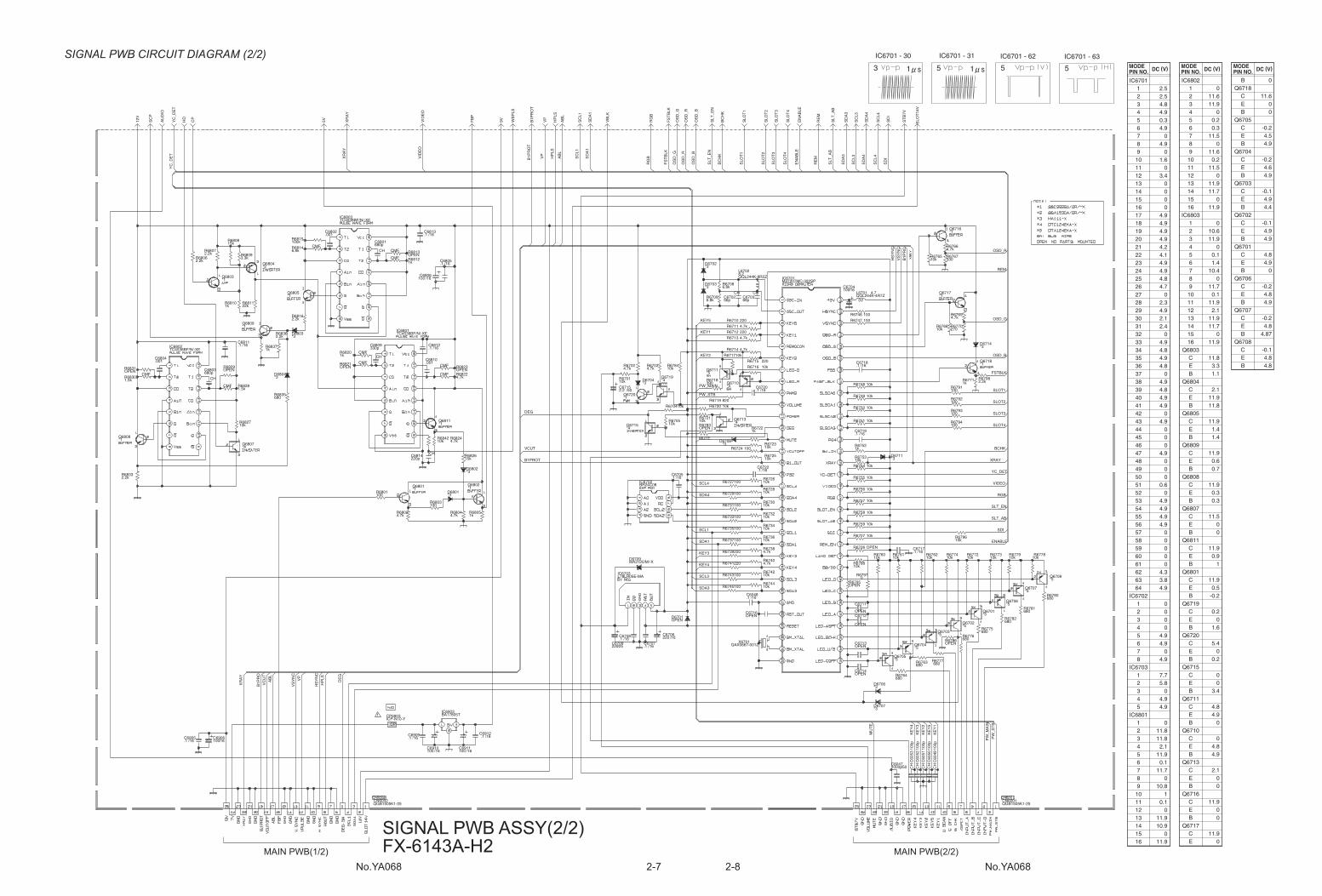
No.YA068 No.YA068
MODE DC (V)PIN NO.MODE DC (V)PIN NO.
MODE DC (V)PIN NO.
IC6701 1 2.5 2 2.5 3 4.8 4 4.9 5 0.3 6 4.9 7 0 8 4.9 9 0 10 1.6 11 0 12 3.4 13 0 14 0 15 0 16 0 17 4.9 18 4.9 19 4.9 20 4.9 21 4.2 22 4.1 23 4.9 24 4.9 25 4.8 26 4.7 27 0 28 2.3 29 4.9 30 2.1 31 2.4 32 0 33 4.9 34 4.8 35 4.9 36 4.8 37 0 38 4.9 39 4.8 40 4.9 41 4.9 42 0 43 4.9 44 0 45 0 46 0 47 4.9 48 0 49 0 50 0 51 0.6 52 0 53 4.9 54 4.9 55 4.9 56 4.9 57 0 58 0 59 0 60 0 61 0 62 4.3 63 3.8 64 4.9 IC6702 1 0 2 0 3 0 4 0 5 4.9 6 4.9 7 0 8 4.9 IC6703 1 7.7 2 5.8 3 0 4 4.9 5 4.9 IC6801 1 0 2 11.8 3 11.8 4 2.1 5 11.9 6 0.1 7 11.7 8 0 9 10.8 10 1 11 0.1 12 0 13 11.9 14 10.9 15 0 16 11.9
IC6802 1 0 2 11.6 3 11.9 4 0 5 0.2 6 0.3 7 11.5 8 0 9 11.6 10 0.2 11 11.5 12 0 13 11.9 14 11.7 15 0 16 11.9 IC6803 1 0 2 10.6 3 11.9 4 0 5 0.1 6 1.4 7 10.4 8 0 9 11.7 10 0.1 11 11.9 12 2.1 13 11.9 14 11.7 15 0 16 11.9 Q6803 C 11.8 E 3.3 B 1.1 Q6804 C 2.1 E 11.9 B 11.8 Q6805 C 11.9 E 1.4 B 1.4 Q6809 C 11.9 E 0.6 B 0.7 Q6808 C 11.9 E 0.3 B 0.3 Q6807 C 11.5 E 0 B 0 Q6811 C 11.9 E 0.9 B 1 Q6801 C 11.9 E 0.5 B -0.2 Q6719 C 0.2 E 0 B 1.6 Q6720 C 5.4 E 0 B 0.2 Q6715 C 0 E 0 B 3.4 Q6711 C 4.8 E 4.9 B 0 Q6710 C 0 E 4.8 B 4.9 Q6713 C 2.1 E 0 B 0 Q6716 C 11.9 E 0 B 0 Q6717 C 11.9 E 0
B 0 Q6718 C 11.6 E 0 B 0 Q6705 C -0.2 E 4.5 B 4.9 Q6704 C -0.2 E 4.6 B 4.9 Q6703 C -0.1 E 4.9 B 4.4 Q6702 C -0.1 E 4.9 B 4.9 Q6701 C 4.8 E 4.9 B 0 Q6706 C -0.2 E 4.8 B 4.9 Q6707 C -0.2 E 4.8 B 4.87 Q6708 C -0.1 E 4.8 B 4.8
!
SIGNAL PWB ASSY(2/2)FX-6143A-H2 MAIN PWB(2/2)MAIN PWB(1/2)
C6048
IC6701
IC6802
IC6801
IC6803
Q6811
C6704
R6774 R6772 R6773
Q6706
Q6701
Q6702
R6776R6786
D6714
R6775
R6782
R6779 R6778
Q6708
Q6707
R6781
R6780
C6711
C6712
C6713
C6714
C6047
CP6903
Q6711
Q6710
CN6002 CN6001
IC6703
IC6702
R6717
R6716
R6718
R6719
R6724
D6711
R6722
D6701
R6742
R6740
R6738
R6736
R6735R6734
R6732
R6730
R6728
R6726
R6743
R6745R6744
R6714
R6710
R6739
R6741
Q6713
C6705
Q6716
Q6717
Q6718
R6766
R6767
R6769
R6770
R6771
R6765
R6768
R6748
R6749
R6759
R6712
R6750
R6751
D6708
C6906
R6795
Q6715R6705
R6720
R6783
R6704
C6717
R6721
C6715
Q6809
C6813
C6812C6811
D6706
C6718
R6791
R6792
R6793
R6794
C6719
R6707
R6706
R6788
C6716
C6722
Q6807
D6707
C6720
R6796
C6814
R6797
X6701
L6701
L6702
C6703
R6708
R6709
D6702
D6703
R6798
C6706
C6709
C6708
C6707
Q6719
Q6720
D6704
R6702
R6701
R6703 R6784
R6760 R6761 R6762
Q6703
Q6704
Q6705
R6764
R6763 R6777
R6733
C6702
R6752
R6754
R6755
R6756
R6715
IC6903
C6911C6910
C6912C6909C6905
R6713
R6711
R6747
R6746
R6731
R6729
R6727
R6725
R6737
D6709
R6758
R6723
R6801
R6802
R6803
R6804 R6805
Q6801 Q6802
D6801
D6802
R6753
R6757
C6806
C6805
C6804
R6833
C6803
R6828
R6807
C6809
R6820
R6822
C6810
Q6805
R6824
R6809R6806
D6804
D6803
R6808
R6826
Q6808
R6827
R6829
R6830
R6831
Q6803
Q6804
R6810 R6811
R6821
C6801
C6802
R6812
R6813R6814
R6815
R6836
R6835
R6816
R6837
R6823
R6842
C60
53
C60
52
C60
51
C60
50
C60
49
12V
SC
P
AU
DIO
YC
_DE
T
HD
CP
5V XR
AY
VID
EO
FB
P
9V WB
PLS
B1P
RO
T
VP
HP
LS
AB
L
SC
L1
SD
A1
VB
LK
RG
B
FS
TB
LK
OS
D_G
OS
D_R
OS
D_B
SLT
_EN
BC
HK
SLO
T1
SLO
T2
SLO
T3
SLO
T4
EN
AB
LE
RE
M
SLT
_AB
SD
A3
SC
L3
SD
A4
SC
L4
SD
I
ST
B7V
SLO
T14
V
/16
M37207MC-322SP
TC4538BF/N/-XE
TC4538BF/N/-XE
TC4538BF/N/-XE
/16
/50
CPICP-N10-Y
QGB1505K1-25 QGB1505K1-25
L78LR05E-MA
BR24C08
/16
/16
/16
/50
/16
/16/16
/16
/16
/16
/16
CH
QAX0667-001Z
QQL244K-4R7Z
QQL244K-8R2Z
CH
/16
/25
/16
/16
CH
BA17805T
/16/16
/16/16/16
MA3120/M/-X
/16
/16
CH
CMF
CHCMF
CMFCMF
CMF
CH
CMF
CMFCMF
CMF
CH
CH
CH
CH
CH
.1
*1
100
10k 10k 10k
*5
*5
*5
680OPEN
*3
680
680
10k 10k
*5
*5
680
680
OPEN
OPEN
OPEN
OPEN
1000p
*5
*5
10k
10k
390
820
100
*3
1k
OPEN
10k
4.7k
4.7k
10k
100 10k
10k
10k
10k
10k
100
100 10k
4.7k
220
220
220
*4
.1
*1
*1
*1
4.7k
330
4.7k
270
1k
10k
10k
10k
10k
10k
220
10k
10k
*3
100
OPEN
*410k
10k
OPEN
10k
.1
10k
2.2
*1
.1
.1.1
*3
.1
100
100
100
100
.1
10k
OPEN
10k
OPEN
.1
*4
*3
.1
10k
220p
0
4.7
8.2
68p
6.8k
6.8k
*3
*3
2.2k
220
220
.1
.1
*4
*1
*3
4.7k
10k
4.7k 10k
10k 10k 10k
*5
*5
*5
680
680 680
100
56p
1k
10k
10k
10k
220
100100
.1.1.1
4.7k
4.7k
100
100
100
100
100
10k
100
10k
10k
100
4.7k
100
4.7k 1k
*1 *1
*3
*3
10k
10k
100
.1
.001
2.2k
680p
1.5k
2.2k
330p
1k
4.7k
.001
*1
4.7k
3.3k2.2k
*3
*3
15k
15k
*1
10k
OPEN
1.5k
OPEN
*1
*2
1k 22k
OPEN
680p
.001
1k
OPEN6.8k
100k
2.2k
680
2.2k
1k
OPEN
10k
100p
100p
100p
100p
100p
KEY5
OSD_B
SDA1
YC_DET
REM
MUTE
PW_MAIN
BCHK
B1PROT XRAY
SLT_AB
SLT_EN
KEY2
RGB
VIDEO
ENABLE
KEY4
PW_STB
KEY3
KEY1
OSD_G
FSTBLK
VCUT
OSD_R
SLOT1
SLOT2
SLOT3
SLOT4
SCL1
DEG
SDA3
SCL3
SCL4
SDA4
SDI
VID
EO
HP
LS
AB
L
BC
HK
SLT
_EN
OS
D_B
YC
_DE
T
OS
D_R
OS
D_G
FS
TB
LK
VP
RG
B
VS
YN
C
B1P
RO
HS
YN
C
XR
AY
SLO
T1
SD
A1
SC
L1
B1P
RO
T
SD
I
SC
L4
SD
A4
SC
L3
SD
A3
SLT
_AB
RE
M
EN
AB
LE
SLO
T4
SLO
T3
SLO
T2
KE
Y1
KE
Y5
KE
Y2
KE
Y3
KE
Y4
HS
YN
C
MU
TE
HP
LS
B1P
RO
VC
UT
AB
L
VS
YN
C
VP
XR
AY
DE
G
PW
_MA
IN
PW
_ST
B
3
IC6701 - 30
1 5
IC6701 - 31
1
IC6701 - 63
5
IC6701 - 62
5
SIGNAL PWB CIRCUIT DIAGRAM (2/2)
2-82-7
,
~-
~ l::,.
-+~
-
p +
,..j..
L r , .ii.. .I., r.,;,
--------~ --~ ~ ~
,.
'........--.----+-1 ~l I l~:,:·:: .+, _J L -i osc_ou,
~----- -".M,+-+-----lj1" )KEY5
+ov
HSYNC
VSYNC
4::0N 1,- -~ l,=a- ---t--".M,+- -----\S)j KEY2
OSD-R
0S0-G 0
0S0-B ...
,
~ ..
" ..
,
~~~ i I u-------1---1
"'~1
BUFFER
~
s, r~,~;1 f CED_G
- ·~ " , H-t,---,VV,.-::_-::_-::_-::_-::_,-::_-;;:,"v,·-=-~',::,_J::,,.~::_-_-_-_,l,•:.)l~:A
I FAST-SLK (l'iJ--------+--++--~
-~INv::.~-=.tt-t-V,-;;:.-::_-::_-::_-::_-::_~-::_-::..,-----l.,,,VOLUME ~. I ~----::)_ POWER
:,~ INVERTER ~ DEG
SLSCAO
SLSCAt j
SLSCA2
SLSCA3
• ..,. ., MUTE
1,,- ---+--+-t-t---+----------+- +>+- ------V ,-,.J---< l.O.,) VCUTOFF
PO< .. ..
81 -I N lo---'Wr---t--
l'-- --t--+-+-+-+--+------ 1-H- -------!() a<-0uT xa,v(il)----'VV'v<0--,----*-+-~>--+-------1
H-+- ------ - ::1---- ,_e)p32
l'+-----1v---o- 1 - e.,) 5CL4
YC-DET r,,>>-+-----+----+-------- -'I
v1oe:or,.,,-+-1 ----1-----1----------~1
• l'f- ----W\.--- -- -O) ., SOA4 RGB (~)-+-----f----f----------'I
r,:,,__:~~-=--=--=--=--=--=--=-~~-=--=--:::.~r:.__S.,) SCL2 SLOT_EN fS>-+-----t----t----------'I
eM O ~-+++----'VVv----+--- <JSOA2 SLOT-AB fV-+-----t----1----------~I
l't-- - -.- --1v--- 1o--<,i)SC U SDI • j
l'f-----t-,-...,.,_,.,,._ _____ iil) SOA1 FEM-EN(\,'-+-----+----+--------~
no te • -----
* 1 , 2SC3928A/QA/-X
*2 ' 2SA1~30A/QFV-X
*3• MA.111-X *4 • OTC124EKA- X *S • OTA124EKA -X aw, BUS WIRE OPEN , NO PARTS MOUNTEO
l~--<-+~ VVv------ !alKEY3
lr- --<-+~VVv--- 10- -a )KEY4
l'f-----t-f--'VV\.------ !l)SCL3
r-'\Mr--- ..--,1-;:i.., LANO. DETtj ~ ...,.,_A..-1-0--.--.--.-.+---+--<>-+-+--+-<>-+-+--+------
50/00 l)-,r'!;I'
LED_D (l/iJ-+---+--+--+-+--+-+,f-+-+-+-+-+-+--+-t- >-+r'!;l,1--<"f' i..::,' J '1---+-t- -'VV\.---.__ ,_,so,a
0-+- -t-+--- -i: :1-< ---@ )SND
>-I f--( ~ RST -DUT I t--+-----1--t-+----+--- ru)FESET
z)i :: =~ ,¥ rM
m;r---< ~ .. _,,,c JJL--.( a> Bt•LXTAL
>---(~SND -~
LED-C «>-->-~-~t-+--+-+--<-+--+--+--+--+--+-+- a--F.-, -1.!:,~ '
LED-Bf>r+>-l- l~i--10- +--+-+--<-+--+-l---+--+-, r'/;-+,-»'H I.!:
LED->' >-tl-1 ,r'!:, 'i..::,] ,F. , ' i.::: J :'
L::~::<Sr+----+-1--t-,-r':; .,-+-l, _.a-, i Jr ~ -(~ >-1_ 11-1--..-~J:;,;f" '. I!:, 'VVv--
LED-C OFF -; 1---1 ~ ~-----~
-~ 1 .~
1 _J

No.YA068 No.YA068
MODE DC (V)PIN NO.MODE DC (V)PIN NO.
IC1401 1 0 2 11.4 3 -10.2 4 -11.4 5 0.2 6 11 7 0 IC1451 1 5 2 3.2 3 3.2 4 -11.4 5 0.4 6 11.1 7 11.1 8 11.5 IC1901 1 1.7 2 0 3 163.1 4 18.3 5 0 IC1902 1 174 2 174 3 174 4 174 5 0 6 -7.7 7 0 8 6 9 -6.7 10 -7.6 IC1905 1 43.9 2 42.9 3 3.4 4 18.3 IC1906 1 7.4 2 6.3 3 -2.7 4 6 IC1971 1 11.9 2 0 3 8.9 IC1973 1 11.9 2 15.5 3 0
Q1452 C 5.7 E 0 B 0 Q1453 C 0.5 E 5.7 B 5.1 Q1454 C 6.5 E 0 B 0.5 Q1402 C 11.4 E 0 B 0 Q1504 C 0.3 E 0 B 0.2 Q1505 C 3.1 E 0 B 0.3 Q1501 D 36.8 G 2.6 S 0 Q1521 C 0 E 58.7 B -0.1 Q1571 C 0 E 0 B 0.6 Q1933 C 42.9 E 6.9 B 7.4 Q1932 C 0 E 53 B 52.8 Q1934 C 7.7 E 0 B 0 Q1935 C 4.4 E 1.2 B 1.9
DY01DEF. YOKE
RY1401
R1955
R1956
DEG.SW
RUSH.SW
STB7V
SCAN
E/W.OUT
IC1901
R1906
R1907
C1916
C1909
C1910
K1901
C1912
C1993
C1913
D1903
D1904
R1908
R1909C1914
CN1003
H.O
UT
GN
D
H.O
UT
C1944
D1905
C1908
LF1902
C1917
R1904
D1902
C1911
C1907
D1901 H1007
R1905
C1904
C1991
R1902
9V
12V
SLOT14V
IC1905
R1948
R1949
Q1933
C1941
D1939
D1940
R1954
R1951
R1950
VR1901
L1974
L1971
D1942
R1958
C1942
Q1932
R1959
R1960C1943
D1941
CP1974
D1974K1973
C1978
K1972D1973 C1408C1977
D1972
D1971C1971
C1975
C1976
H1003
C1992
R1584
CP1972
R1974
R1972
C1985C1986
C1983
C1984 C1982
H1001
R1464
D1582
R1989
D1575
C1577
D1577
R1574
C1575
R1575
D1576
Q1571
R1990
C1905
R1576 R1577
C1906
C1572
R1571
C1576
R1581 C1571
D1571
D1572
D1573
D1574
C1406
C1409
A.VCC
L1972CP1977
R1505
D1524
Q1501
C1502
R1506
C1503
C1563
T1501
Q1521
R1521
C1903
T1901
T1902
TP-B1
IC1401
C1987
D1943
D1581
CN10E2
D1979
CN100U
D1562
D1551
D1555
R1903
R1559
R1558
R1557
CP1971
IC1973
C1403
IC1971
D1401
R1551
D1406
C1555
L1551
R1554
R1553
R1552
D1552
D1553
C1556
C1527
C1557
D1407 C1552
C1573
R1454
IC1451
R1458
C1404
R1456
R1457
R1455
R1460
R1459
Q1452
Q1454Q1453
C1452
D1403
C1402
R1408
C1562
R1410
R1404
R1403
D1402
Q1402
R1401
R1411
R1405
7V
B1.PROT
R1406
D1404
R1407
D1578
R1578
Q1505
R1507
R1508
C1915
TH1901
C1528
C1939
C1938
H1005
H.SYNC
R1910
IC1902
CN10HV
D1906
CN1004
T1551
R1524
D1980
H.OUT
C1401
C1407
R1510R1509
Q1504
R1413K1974
V.SYNC
VHSS
V.GARD
FBP
ABL
V.CUTOFF
V.DRIVE
V.POSI
CN1DEG
H1002
C1405
R1412
R1414
D1983
R1928
CN10PW
C1574
D1554
C1990
R1463
F1901
C1901 C1902
LF1901R1920 D1920
C1930C1931
C1932
C1933
CP1975
C1934
D1921
R1921
R1923
D1922
D1923
R1924
R1922
C1936R1927
R1926
C1935
R1925
D1924
C1937
D1977
IC1906R1980
R1982
C1988
R1984
R1983
RY1901
RY1902
D1981
D1982
Q1934
Q1935
R1985
R1987
R1986
R1988
D1978
D1984
L1973
C1458
C1994
R1977
C1980
CESK024-001
MFQRT029J-R56
MFQRT029J-1R0
STR-F6653
QRM059J-R27
1/2W
R1/2
QCS31HJ-471Z
2kVQCZ0325-561
CE42050-001Z
/50QEHR1HM-476Z
400VQCZ9079-102
RGP10J-5025-T3
RGP10J-5025-T3
1/2W
R1/2
QCB31HK-102Z
QGBA001K1-04
/100QFLC2AK-102Z
QCB32HK-222Z
QQR1217-001
2WQRL029J-683
RU1C-LFC4
/400QEZ0550-337
AC400VQCZ9078-102
D3SB60 CM42862-00H
AC400VQCZ9078-102
AC400VQCZ9079-222
QRF154K-4R7
TLP721F( D4-GR)
2SC2229/Y/-T
MA4068N/Z1/-T2
QRA14CF-4701Y
QRA14CF-1502Y
QRA14CF-1502Y
QVP0087-102Z
QQL26AK-560Z
QQL26AK-560Z
/16
2SA949/Y/Z1-T
/50QEHR1HM-105Z
MTZJ7.5S-T2
CPICP-N50-Y
RU3YX-LFC4CE42050-001Z /25
QEHR1EM-108Z
CE41433-001ZRU3YX-LFC4
MM/25
QEHQ1EM-228
RU30-F1
RU30-F1/500
QCZ9078-152
/100QEZ0203-227
/100QEZ0203-227
LC32111-001A
400VQCZ9079-102
1/2WFR QRZ9011-4R7
CPICP-N38-Y
CP
2WQRL029J-220
2WQRL029J-220
/25QEHR1EM-477Z
/16QEHR1CM-477Z
/25QEHR1EM-108Z
/16 / 16
CEHT12N-026PS
MTZJ7.5S-T2
1SS244-T2
1SS244-T2/25
QEHR1EM-107Z
AC400VQCZ9078-102
AC400VQCZ9078-102
/100QEHR2AM-106Z
MTZJ6.8C-T2
/100QFLC2AK-103Z
MY
QFLC1HJ-103Z
QQL26AK-560ZCP
ICP-N75-Y
DBSN304-TQCB32HK-681Z
1/2W
R1/2
/50
/50
QQR1032-001
2SD2645-YD
1/2W
R1/2
QFZ9036-104
QQS0257-001
QQS0130-001
CM42818-001
LA78041
/35QTMM1VM-108
QUB190-28FPKT
RU3YX-LFC4
CHHB04-300U-G
RGP10J-5025-T3
MTZJ6.8C-T2
OMR3
1/2WR1/2
CPICP-N10-Y
CP
BA12T
MM
BA17809T
FR
QRZ9017-2R2
/160QEHQ2CM-107
QQLZ026-260
1/4W
FR
QRZ9017-4R7
2W
FR
QRZ9024-R82
2W
FR
QRZ9024-R82RU30-F1
RU30-F1
/16QTMM1CM-478
/100QEHQ2AM-477
/16QTMM1CM-478
MTZJ18A-T2
NJM4560D
MM
2SD1267A/QP/
1SR35-400A-T2
/35QEHR1VM-477Z
MM
QFLC1HJ-223Z
2WQRX029J-R47
RD62E/B/-T2
2SC3311A/QR/-T
1/4WQRA14CF-1600Y
1W
OMR1
1/2W
R1/2
2W
OMR2
2W
OMR2
MYQFLC1HJ-103Z
QAD0132-4R5
2kVQCZ0325-561
/50QEHR1HM-475Z
MY
QFLC1HJ-103Z
CEHT11B-005QS
STR-L472/F7
QGZ8001C1-04
QGBA001K1-04
QQH0178-001
OMR3
QRL039J-102
NJM431L-T
MYQFLC1HJ-102Z
CE42050-001Z
WJJ0466-001A
LC31843-001A
/16QEHR1CM-107Z
1/4WQRA14CF-8200Y
RD4.3E/B2/-T2
1/2W
R1/2
QGA7901C1-02
/25QTNC1EM-107Z
MTZJ6.8C-T2
AC400VQCZ9079-222
QMF51D2-5R0-J1
QFZ9036-104 QFZ9036-104
QQR0527-00210W
QRF104K-3R9S1WB/A/60-4101
QCZ9054-472QCZ9054-472
QCZ9054-472
/400QEHQ2GM-226
QMFZ043-2R0Z-J1
QCZ0325-222
RU1C-LFC4
1/2W
R1/2
AU01Z-T2
AU01Z-T2
1/2W
R1/2
1/2W
R1/2
1/2W
R1/2
1/2W
R1/2
2kVQCZ0325-151
1SS133-T2
QCB31HK-222Z
RU3YX-LFC4
PC123Y22FZ 1/2W
R1/2
QFLC1HJ-473Z
QSK0119-001
QSK0119-001
RU3YX-LFC4
QQL26AK-220Z
QRZ9024-R33
/16QEHR1CM-108Z
MM
N
.56
1
0.27
680
470p
OPEN
560p
47
1000p
OPEN
2.2k
OPEN.001
.001
*3
.0022
OPEN
68k
330
.001
22
.001
.0022
4.7
18k
150k390p
*3
4.7k
15k
15k
1k
56
*3
2.7k
100
18k
5.6k1
1000
.472200
.0015
220
220
1000p
4.7
22
22
470470
1000
470 100
OPEN
68
220p 1k
100
1k
*3
*1
68
.001
1k 3.9k
.001
10
560
220p
3.3k .0068
*3
*3
*3
.01
.01
56
12k
*3
680p
1.5k
2.2
2.2
180
1000
*3
*3
68k
4.7k
18k
27k
.82
*3
2.2
*3
100
24
4.7
.82
.82
4700
470
4700
OPEN
1
4.7k
680
.82
1k
OPEN
8.2k
680
1k
*1
*2
100p
470
OPEN
.022
33k
.47
1.2k
160
1k
100 1.5
*3
10k
OPEN
OPEN
*1
180
180
0.01
560p
4.7
.01
3.3k*3
1k
.001
OPEN
10k10k
*1
1k
100
820
680
220k
100
.0022
1k
3.9
.0047.0047
.0047
22
.0022220k
68
2.7k
560k
470p2.7
680
150p
4.7k
.0022
330
1k
0.047
10k
4.7k
*3
*3
*1
*1
10k
10k
680
680
*3
22
100p
100p
.33
1000
SCAN
GND3
GND2
GND2
GND2
GND1
GND2
V.DRIVE
GND1
V.GARD
FBP
GND1
VHSS
V.CUTOFF
V.DRIVE
GND2
V.POSI
V.SYNC
H.OUT
VHSS
H.SYNC
B1.PROT
A.VCC
SLOT14V
12V
9V
E/W.OUT
GND2
GND3
GND1
GND3
GND1
GND2
STB7V
RUSH.SW
GND1
GND2
GND3
GND2
7V
GND2
GND2 GND2 GND2
GND3
GND1
GND2
GND3
GND2
GND2
GND2
B1.PROT
GND2
GND2
GND2
DEG.SW
GND1
GND2
GND3
GND2
GND1
GND2
GND2
GND3
GND2
GND2
GND3
GND2
GND1
GND2
GND2
GND2
GND2
GND2
GND2
GND2
GND2
GND2
GND2
GND2
GND2
GND2
GND2 GND2
GND2
GND2GND2 GND2
GND2
GND2
GND2 GND2
GND2
GND2 GND2
GND2
GND2
GND2
ABL
GND2
GND2
GND3 GND2
GND2
GND2
GND2
GND2
V.SYNC
GND2
GND2
GND2
GND2
GND2
GND2
V.POSI
H.OUT
GND2
E-W
. OU
T
X-R
AY
-1
X-R
AY
-2
MAIN PWB ASSY(1/2)FX-1187A-H2
SUB DEF PWB SUB DEF PWB
SUB DEF PWB
IC1401 - 5IC1401 - 3,6 Q1501 - DQ1501 - G Q1521 - B
40 609 2
T1551 - 5
180 80180 30800T1551 - 4 T1551 - 6 T1551 - 7
20
Q1521 - CIC1401 - 1,7
0.8IC1451 - 1
4
IC1451 - 3
2.5
Q1454 - C
4
MAIN PWB CIRCUIT DIAGRAM (1/2)
!
!
!
!
!
!
!
!
!
!
!
!
!
!
!
!
! !
!
!
!
!
!
!
!
!
!
!
!
!
!
!
!
!
!
! !
!
!
!!
!
!
!
!
!
!!
2-9 2-10
~\Co o, ~ 1~ --6.-- -6.- -- -- -6.- -- -- -- -- -- -- -- -~- -- -- -- -- -- -- -- -- -- -- -- -- -- -- -- -- -- -- -- -- -- --
~ o+Ull---!ti-i-,;:---£,~-~f,-,~ 6. ,r*i ::6. 6. - ,6. ,,---(''4--l'~M-+--------,=--<~.--=-~'IT'--_____,~~~~~~~~~~~~~~~~~~~~~~~~---=,,
~ ci.::ITCH I 6 6 6 ~ 1 + ¥' I :: t:::,. f - *··· ~ = :,__... f .. 0 QSW0699-00i f vvv-- • .: ;__ 12
§_~ ·~
I ii .J,, & U~5CA N-S•
3f'.-' i
I'"'"' * 1 , 2SC3311 A/GFI/ - T •2 , 2SA 1309A/GFV-T •3 , 1SS133- T2 *4 , DTC124ESA-T I OPEN • NO PARTS MOUNTED
I I TM-+t150CGUA I FX-11B7A TM-+t150CGEA
TM--H150CGC A
f
-1 -
..
f ~ ••
+ t:::,.
t:::,.
-2 ,_
l ·: : -
L : : 7-
1 ·: -:
L : : 6
·-g -7 ,-. '
: 6 .: 0
.l i:: f- 11
)-. 12
T ~
. ~. (8
' ' FEEO SACK ~
ro~
t:::,. --
t:::,. ~- .-.-.a
t:::,.
~- -
r;t
[~ ~ ~ ~ ~ ~ ~ : ~.!J f. ~ 1 .. 1.1r -~ + ~
> ,.., '
)
+
::
If--
" ~
.. ti I T If---
I u EW-ORIVE
a 1 + ,
1 -·-·,'--+-·-__ ___________ ,
1------------i--> >-JI-
' . I I I I I
~ I
I I I
---------,
' ' 1-:f~~-----------------------------------~ -----I
·-fl
I I I
,-------k
t:::,.
t:::,.
ALOIO-VCC
~
etl53VI
,: l I
" '
L _________________ _ i "ij ------>?
/ I PROTECTION : I r----:f:=:::;-= :r-- 1 I I ,.- I
! ~ ! I Vc:c .l. ~e, I
l_-:1=_2~=5-6- 7>:_: I
t-EATEA
I s. ovrms I
I
6FBT
£, ·-·-· " EHV
I ,II->" n ~~ FOCUS
......... -~f4 ± ± i] '+---<)"-> 1tl SCREEN
~-~
>-+--o• •
---- ~ '' f 1 ~ ~---++-----+------+i- f-..---,.+ t:::,.---,,,,,;-----+L_;.JIH--,..:;---<>----' j-----------cr r=,[ 1~-1 n-_ ---+--++--ir' I
II
'55244 I I -T2 l~
,--------'O-,r-----0'•~ ,.., I JJ I > HEATEA ]
t:::,. ~---++--f--- -.
H.OIJT r---,- ./
n L
2 GND 3 N.C ~- .-.
- ~ 6 -'VY',----0--+-+-+---1 ~ <<I I H~
Z: ti TO CAT SOKET P8 ASSY
"~
I
1~ !m
16.~
I 2 -1 072 ,~---------+-+------------+-------+-+----------------+-, I
1~ .,.EAAOR AMP I, '
, ;j,OEHR,CM .
,~ I 't:::,. .. ,6. .
~ ' r · ~ , I
I SOLAT ED '" I .J: ~\. GARO 1 •· [c•rno,[r., JTJ. [c•rno,[ G " _J LIVE
~ 1- 1 '" ~ ,.., ,----~------ ~ .!l-
_________________________ _J L_J L_J

No.YA
068No.YA
068
MO
DE
DC
(V)
PIN
NO
.
IC1411
1
6.3
2 4
3
0.5
4 0
5
4.8
6 8.9
7
3.8
8 0
9
0.6
10 6
11
1.4
12 0.7
13
0
14 4.1
15
4.2
16 0
17
3.4
18 4.5
19
0.7
20 1.7
21
1.5
22 3.9
23
4.6
24 2.9
IC1601
1
11.5
2 5.1
3
0
4 3.5
5
5.6
6 5.7
7
0
8 5.8
9
12.6 Q
1431
C
4.4
E
0
B
0 Q
1403
C
8.9
E
3.5
B
4 Q
1551
C
3.8
E
0
B
0 Q
1573
C
0
E
8.9
B
8.9 Q
1574
C
8.9
E
0
B
0 Q
1401
C
3.8
E
0
B
0.6 Q
1405
C
8.9
E
3.1
B
3.8 Q
1451
C
3.2
E
0
B
0.5 Q
1601
C
11.5
E
4.9
B
5.8 Q
1602
C
5.1
E
5.1
B
4.5 Q
1603
C
0
E
0
B
0.7 Q
1604
C
5.6
E
0
B
0
!
!
RU
SH
.SW
SLO
T14V
ST
B7V
12V
A.V
CC
H.S
YN
C
V.S
YN
C
V.G
AR
D
C1416
C1415
C1417
C1410
AB
L
IC1411
C1451
IC1601
R1435R
1436
CP
1973
7V
R1602
FB
P
B1.P
RO
T
VH
SS
C1602
C1605
C1616
C1601
R1431
R1611
C1611
R1604
C1603
C1617
D1606
R1621
R1620
C1618
Q1604
C1612
R1601
R1612
R1613
C1613
D1603
R1432
R1614
C1615
C1614
R1603
Q1602
Q1601
Q1603
D1605
R1619
R1618
R1617
CN
100S
Q1431
9VDE
G.S
W
C1414
V.C
UT
OF
F
R1422
R1420
R1421
D1405
H.O
UT
R1415
R1560
D1556
R1555
Q1451
R1451
R1416
C1418
R1417
Q1401
SC
AN
R1453
D1408
K1401, K
1402
V.D
RIV
E
E/W
.OU
T
V.P
OS
I
R1423
Q1403
R1424
CN
1002
Q1573
R1579
R1580
R1582
D1580
D1579
C1578
R1583
Q1574
C1431
R1434
R1433
R1561
R1562
C1561
R1419
R1563
R1564
CN
1001
R1622
R1418
D1409C
1413
R1409
K1401
R1605
C1421
C1604
C1455
C1412
Q1405
R1429
C1423
R1565
D1557
R1566
C1564
C1979
C1619
Q1551
R1402C
1424
C1457
C1454
CN
100A
R1452
R1428
R1567
MY
MM
MY
MM
TA
1241AN
MM
AN
5265
QU
Y153-050Y
1/2WQ
RK
126J-220X
/25/50
/50
/50Q
EH
R1H
M-106Z
MM
/35
MY
MY
/25
1/2W
R1/2
/25Q
EH
R1E
M-108Z
MY
MT
ZJ11A
-T2
CH
41169-003Y
/16Q
BT
C1C
K-225Z
MT
ZJ6.8C
-T2
1/2W
R1/2
/35
MA
4022/L/-T2
QG
B1505J1-25
MA
4068N/Z
1/-T2
/10Q
EH
R1A
M-227Z
2SC
2785/JH/-T
QC
B31H
K-332Z
QG
B1505J1-25
QR
Z9021-100
MT
ZJ12C
-T2
MM
QC
B31H
K-103Z
/35Q
EH
R1V
M-476Z
MY
/25
/25
QG
F1220C
2-19
MY
.022
1
.001
.1
.1
100
100
22
10002.2
4.7
.01
22k
330
10
12k.12
47*356k
22k
.01
*1
.1
1k
10k8.2k
220
*3
6.8k
4.7
1000
.047
5.6k
*2*1
*1
47
150k
1.2k
*4
2.2
22k
10k
1k
22k
1M
*3820k
*1
3.9k
680
47
1k
*1
1.5k 820
*1220
*2
22k
22k
820
22010k
.0033
10k
10k47k
22k
270p
10k
10k
10k
10
100
.1
10k
100
100p
.01
100p
100p
*1
1k
4722k*3
2.2k
.022
470
2200
*4
0
100p
OP
EN
100p
OPEN
10k
1M
GN
D2
GN
D2
GN
D2
VH
SS
B1.P
RO
T
H.O
UT
FB
P
V.C
UT
OF
F
RU
SH
.SW
V.P
OS
I
SLO
T14V
ST
B7V
12V
H.S
YN
C
V.S
YN
C
V.G
AR
D
E/W
.OU
T
V.D
RIV
E
SC
AN
DE
G.S
W
7V
GN
D2
GN
D2
9V
GN
D2
GN
D2
GN
D2
GN
D2
GN
D2
AB
L
GN
D2
GN
D2
GN
D2
GN
D2
GN
D2
GN
D2
GN
D2
GN
D2
GN
D2
GN
D2
GN
D2
GN
D2
GN
D2
GN
D2
GN
D2
GN
D2
GN
D2
GN
D2
GN
D2
GN
D2
GN
D2
GN
D2
GN
D2
GN
D2
GN
D2
GN
D2
GN
D2
GN
D2
GN
D2
GN
D2
GN
D2
PW_STB
INPUT_D
INPUT_B
ASPECT
C.OFF
KEY1
KEY2
KEY4
PW_MAIN
INPUT_C
INPUT_A
KEY4
B.CHK
U.SCAN
KEY5
KEY3
FBP
VHSS
PW_STB
E/W.OUT
SCAN
PW_MAIN
INPUT_D
INPUT_C
INPUT_B
DEG.SW
H.OUT
B1.PROT
INPUT_A
ASPECT
B.CHK
V.CUTOFF
MUTE
AUDIO
C.OFF
VOLUME
SCL1
SDA1
V.DRIVE
U.SCAN
X.RAY
KEY1
KEY5
KEY2
KEY3
K1402
MA
IN P
WB
AS
SY
(2/2
)F
X-1
187A
-H2
FR
ON
T C
ON
TR
OL P
WB
1.4
Q1451 - C
Q1401 - C
2.8
Q1551 - B
Q1551 - C
54.5
Q1431 - B
Q1431 - C
54.5
IC1411 - 21
1.8
MA
IN P
WB
CIR
CU
IT D
IAG
RA
M (2
/2)
SIG
NA
L P
WB
(2/2
)S
IGN
AL P
WB
(2/2
)
2-122-11
1-----i------- ----- ----------------------------J - -- - - __ , _ - -- - - -- - - -- - - -- - - -- ----i ~
I b l_jJ
: 'El L 11 11 11 ! II I ci
, , 1rn ~ 'Yj ' 1, H ' - ~1::-.: ·: I TI ~ 11 1 bJj ~ I~ ' ~ 3--'wi ~NC V '" ~ HI- ~
,__JI\,) ,_,.; -~ l ~t=· -· ::,, ,_J ' l ./ (/ c::: 1
I
r'[] '"u
IH ~
H,---,
~ 1
~ 1 V. FIAMO
He,,f- . e- ,_ - · - _, , c::: TI
H J ~ i-+- -· - H \ "
~,T ! ~- H ~- ; : :::· ::t - ~<
GJIO fil- =- r'i:: ~ :~ D
··•·• ~· -co- --- rj -.• ,, -/~~~~ ;~_ I ~~ - ~:'.:.
I ~
-· . =~~ ~ v.s, Nc ,:; " " < v. PU.SE r. - l--h-- ~ 'j G,O ,,,[I- I: •~ D
G,O @I=;- ' ::J~ -H.sm: • ' •-i:....:i:-i I
H.ou, r.f-' - I -
.:~ ~~ ~ , · I : 1 ~1 ~ ~ rj
I' " - i 'i' l ~ .. ·- - • i
' R .J • > PH. MAIN ~ ~ - + ~~ j-' ~--=tc;J PILSTB
'
0
• ---=t I NPUT -D
' ~ -T R ~~
VCL::~~~ ~~ _ r+-'
MUTE~
:~[!~ Al.OIO I@: I-
GN~l[fc," ::::t:J
FUSH~~l§:8..r KEV4 ~ KEY3r:
:~:~~ KEY1 _i:
U-C~~:~~ A~~E;;
INF\JT_Afi n
~:~=~~s INPUT_ O w
PW-MAINr..,:: PW_STB L...J
I i-J '-
0~ ~
f-----'vw-'
~
~~
---ii
" +
(ft)
~
y
I
J
I
T -,-
""'
'i -l
6 ] L
~I~+ I I 2 R
I, I
~-...:j:-" - ~
re~ ~~ ~i Ni
=E --l 1--------+
I
JJ ~n~ ~
/, ~ 1-----<:'---+ j N ~ ~ ~ ------,:;r+
f--------1 f----------vv',
c•._[> ~
;!! ln a "•o
~ i : ru- !
i
~ -0 ~1m j
i[m+

No.YA068 No.YA068
!
!
!
!
!
!
C2453
R2461
L2461C2521 D2521 D2522
D2525
CN2003 CN2004
C2522
C2523
C2528
C2524
C2520
C2525
D2523
R2522
R2526
R2525
L2552
R2573
R2572
CN20S1
R2462
L2521 /50N
QEZ0470-475
3WQRG039J-680
QQR1451-001MPPQFZ0196-202 RG4C-F1
RU30-F1
QGBA001J1-04 QGBA001J1-04
QFZ0196-123
QFP32GJ-153
QFZ0196-252
200VQFZ0197-335
/160
OMR2
H.O
UT
GN
D
H.O
UT
OMR2
2WQRX029J-8R2
QQL50AM-8R2Z
1/4W
1/4WQRA14CF-1582Y
CH41770-006
3WQRG039J-680
4.7
68
.002OPEN
.012
.015
.0025
OPEN
3.3
4.710k
1k
8.2
8.2
5.10k
15.8k
68
GND2GND2 GND2 GND2
GND2
GND2 GND2 GND2
E-W
. OU
T
X-R
AY
-1
X-R
AY
-2
SUB DEF PWB ASSYFX-2095A-H2
SUB DEF PWB CIRCUIT DIAGRAM
MAIN PWB(1/2) MAIN PWB(1/2)
2-13 2-14
I I I I I I L...
I CN2003 I
RGP10J-5025-T3
OOR1165 - 005
I CN2004 I
lcN2os1I
0RA14CF - 5101Y
'" [\J
-,
I I I I
[T] "" ID lD ..J (\J ._.,
0 I I z >- >- ~ <( <( (I (I I I
X X

No.YA068 No.YA068
MODE DC (V)PIN NO.
Q3301 C 81.7 E 11.3 B 11.9 Q3302 C 77.2 E 11.2 B 11.8 Q3303 C 78.7 E 11.2 B 11.8 Q3304 C 11.3 E 2.5 B 3 Q3305 C 11.2 E 2.6 B 3.1 Q3306 C 11.3 E 2.6 B 3 Q3307 C 11.3 E 0 B 0
!
!
CN300U
CN300T
Y3001
Y3002
R3307
Q3302
R3309
L3302
R3303
R3341
R3313
C3301
R3308
Q3301
R3306
L3303
R3302
R3305
R3310
Q3303
R3312L3301
R3304 R3311
CN30E1
C3305
R3338
C3306
R3315
D3301
Q3307
R3333
C3307
R3317CN30SC
R3335
Q3306
Q3305
Q3304
R3329
C3312
R3331
C3313
R3325
R3327
C3311
R3321 C3309
R3323
C3310
C3308
C3315
TP-47G TP-47BR3320
R3319
R3318
R3316
TP-EC3317
C3316
R3330
R3332
R3328
R3326
R3324
C3314
R3322
C3303 C3318
R3337
R3336
R3334
R3339
R3340
SK3001
QGA2501C5-04Z
QGA2501C1-10
2W
OMF
2SC4544-LB
2W
OMF
QQL244J-151Z
2W
OMF
/16
QRZ0111-102
2SC4544-LB
2W
OMF
QQL244J-151Z
QRZ0111-102
2W
OMF
2SC4544-LB
2W
OMFQQL244J-151Z
QRZ0111-102
CE41507-001P
/160QEHQ2CM-336
/160QEHQ2CM-336
QRZ0107-105Z
RGP10J-5025-T3
2SC3311A/QR/-T
QCZ0121-102
QRZ0111-474QGZ0017C1-01Z
2SC3311A/QR/-T
2SC3311A/QR/-T
2SC3311A/QR/-T
QRZ0111-102
/50
MY
CE42446-001
OPEN
OPEN
15k
15k
150
100
220k
15k
100
1k
15k
150
100
1k
15k
15k150
100 1k
33
12k
33
1M
220
.001
470kOPEN
120
33p
68
270p
120
82
270p
120 330p
68
33p
33p
220p
100
100
100
1k
OPEN
220p
100
1.5k
1.5k
100
1.5k
220p
100
.01 33p
100
OPEN
220
12k
12k
G
GND2GND2
GND2GND2
GND2
R
GND2
GND2
GND2
B
GND2 GND2
GND2
GND2
GND2
GND2
VCC12V
GND2
BCHK
CRT SOCKET PWB ASSYFX-3075A-H2
SIGNAL PWB(1/2)
MAIN PWB(1/2)
65 70 70
Q3303 - CQ3302 - CQ3301 - C
CRT SOCKET PWB CIRCUIT DIAGRAM
2-162-15
VIDEO - OUT
VIDEO - OUT
I VIDEO-OUT
VIDEO-OUT
I
VIDEO-OUT
VIDEO-OUT
I
0
+
D a: IQ] t§ ~
<! w I
I
+
D V01TURE TUBE(I TC I ~~~AES13X01
G1
I I I I I I I I I I I I I I I I
HV - FOCUS 1
F OCUS2
D
_J

No.YA
068No.YA
068
S4811
R4810
CN
400A
D4801
S4812
S4813
S4814
S4803
S4804
S4805
S4806
S4807
S4808
S4809
S4810
D4802
D4803
D4804
D4805
D4806
D4807
R4803
R4804
R4802
R4806
R4807
D4808
D4809
R4811
S4802
S4801
R4801
R4808
R4809
R4805
R4812
R4813
QS
W0619-003Z
CH
C101N
-19S-L
GL3E
D8
QS
W0619-003Z
QS
W0619-003Z
QS
W0619-003Z
QS
W0619-003Z
QS
W0619-003Z
QS
W0619-003Z
QS
W0619-003Z
QS
W0619-003Z
QS
W0619-003Z
QS
W0619-003Z
QS
W0619-003Z
SLR
-342MG
3FS
LR-342M
G3F
SLR
-342MG
3FS
LR-342M
G3F
SLR
-342MG
3FS
LR-342M
G3F
SLR
-342MG
3F
SLR
-342MG
3F
LC30349-001A
-H
QS
W0619-003Z
QS
W0619-003Z
LC31576-001A
-HLC
31576-001A-H
LC31576-001A
-HLC
31576-001A-H
LC31576-001A
-HLC
31576-001A-H
LC31576-001A
-HLC
31576-001A-H
OP
EN
5.6k3.3k
3.3k
3.3k5.6k
OP
EN
5.6k3.3k
3.3k5.6k
OP
EN
OP
EN
PW
_ST
BGN
D2
GN
D2
INPUT_D
INPUT_C
KEY5
INPUT_B
U.SCAN
INPUT_A
PW_STB
ASPECT
KEY1
B.CHK
PW_MAIN
C.OFF
INPUT_C
INPUT_B
INPUT_A
B.CHK
C.OFF
U.SCAN
ASPECT
KEY3
INPUT_D
KEY4
KEY2
PW_MAIN
FR
ON
T C
ON
TR
OL P
WB
AS
SY
FX
-4092A
-H2
FR
ON
T C
ON
TR
OL P
WB
CIR
CU
IT D
IAG
RA
M
MA
IN P
WB
(2/2
)
2-172-18 ~~=~'.~~ ; I I I I l 1 ~
ASPECT B,CHK
C,OFF LJ,SCAN KEY1 KEY5 KEY2 KEY3 KEY4 GND GND GND GND
~ I . ~ . i I
oc
H .-,Z Gfll IJC z-, '--<
0 /
-
" H z ~ Ile zj"" '----0
'v
/"-<H Hz D-o rnc o_, ~ _oCD
I
~~
[ I
~~
i I @.=::= ~-J
~-=-J
~-=-J
@ ' D Il
rJJc oZ J>o zS!j
®
~
oc
CDo Ilo Hz G)--i
.~'
-00 II J>Il rJJo rn~
'
4

No.YA068 No.YA068
IC8001
CN8006CN8005
C8001
R8001
R8002
Q8001
R8003
C8002
D8001
R8004
R8005
R8013
R8014
Q8002
C8021
Q8003
R8006
R8007
R8008
C8003
R8015
Q8004
R8009
R8010
C8004 R8011
C8012
R8012
Q8005
C8017
R8016
Q8006
R8017
R8018R8019
Q8007
R8020
R8021
R8023
C8005
R8022
C8008
R8024
R8026
Q8008
R8025
D8002
D8003
R8027
D8004
IC8002
R8032
R8029
C8015
C8014
C8013
Y8001
Y8002
R8028
D8005
C8016
R8030Q8009
R8031 C8011
C8018
C8019
C8006C8020 R8034
R8035
C8007
TC74VHC86F-X
QGB2514J1-50QGB1505K1-25
/50
/50/50
CH
/50
/16
/25
/25
NJM2234M-XE
/16
/16
/16
/16
2SC3837K/NP/-X
/50
/50
/50
/50
/50
N
CH
N
10
56k
68k
*1
1k
1
*3
680k
3.3K
5.6k
4.7k
*2
150p
*2
180
22k
27k
OPEN
47k
*1
680
680
3.3 330
.22
0
*1
68p
4.7k
*1
470
1000
*1
5.6k
4.7k
150k
.047
150k
.047
100
100
*1
1k
OPEN
OPEN
3.3K
*3
68k
2.2k
.1
100
100
OPEN
OPEN
3.3K
*3
.1
22k
10k 10
10
10
101500p 150k
1k
10
GND
GND
GND
GND
GNDGND
GND
GNDGND
GND
GND
GND
GND
GND
SLOT PWB ASSYFX-8033A-H2
MODE DC (V)PIN NO.
IC8001 1 5.3 2 5.2 3 0 4 5.3 5 5.2 6 0 7 0 8 4.9 9 0 10 4.9 11 4.9 12 0 13 4.9 14 4.9 IC8002 1 7.3 2 0 3 0 4 0 5 7.3 6 11.9 7 6.6 8 0 Q8001 C 11.9 E 5.1 B 5.7 Q8002 C 0 E 11.6 B 11.9 Q8003 C 11 E 11.8 B 11.2 Q8004 C 11.9 E 8.6 B 9.3 Q8005 C 5.3 E 5 B 0.4 Q8006 C 9.8 E 0.4 B 1 Q8007 C 5.3 E 0 B 0.4 Q8008 C 11.9 E 0 B 0.4 Q8009 C 4.9 E 0 B 0
SLOT PWB CIRCUIT DIAGRAM
SIGNAL PWB(1/2)
2-202-19
!CNB006!
y '1' ~
GND ~ B-Y 9 µ GND ~ R-Y '31 L:'.J GND ~
NC 0 GND ~ A/B '51
L:'.J NC ~
CS/HD ~ GND
eµ VD '71 c'..-J
GND ~ NC [J
I2C-ADR §: ~ NC [] NC ~
C_IN §] GND ~
GP ~ GND ~
NC §] SLOT1 §:
NC §1 SLOT2 ~
NC B SLOT3 §:~
NC ~ SLOT4 ~~
E-AUDIO ~ L='.'.J SLOT-DET ~ NTSCIPAL ~
Fsc ~ YC-DET §]
COLOR/BW ~ 10B0/1035 §]
NC ~ SCL So1 L::.'.'.J 14V ~ SDA '211 14V ~c_J
NC §] 7V ~~ NC §] 7V ~
AUDIO ~ c::::J GND ~ GND '251 GND ~µ
INVERT
I J, > < ij ~ ~ 1 <> > ; < < > BUFFER 1 > > I BUFFER >
ti - 2,ti::' I iH r~ 1 i::i+vv l \b, 3 1::1 ~ r 2/f;'
3 3
) AMP Avv +~ - vv 2Q;> "> -- Kl \b > 1 3
3 <;:j\2 "> <I Av\/v--1• ">
> < <:::J/ < > - 1 > > - < --< T
.. AMP ~ I.
-,...., -
,...., > l +1::1 <> > < >
2/v 1 Kl >
1::1 ) INVERT Kl \b, 2/v,1 3 INVERT AA V V
\!::!, 3 > < <
'> < ,>
> .> . " ~ ..
~ ~
l ,....,
> > >
0----------> < I
-AA
vv
----
EXCLUSIVE OR
.., 1A Vee ~ - -.1
(\J 1B 4B '.'l I "' 1 y 4A ~
"2A 4Y .., ..,
ID 2B 3B 8
ID 2Y 3A Ol
BUFFER
~; 3
~ > ,....,
SWITCH
""IN1
ru SW1
+ zizz
GND CD
OUT"-
--tZl zz
"- GND 3Y CD >--+----+-~\vl'\/y\y------l~N-+~"' IN2 Vee ID>-----
y :o------t.-----~ > <
+ "SW2 IN3 ID --I
ICNB0051
'25 y = ~ GND '23 B-Y l'.:.::'.
§] GND '21 R-Y = ~ GND '19 A/B L.:.:'.§l SYNC '17 12V L.:::..'...
,+., ~ GND '15 5V L:.:'.~ RGB/CMP '13 SLOT1 L:.:'.
§] SLOT2 '11 SLOT3 ~§] SLOT4 'g SCL L:'._0 14V '7 SDI L'._0 SDA
-------G: 7V
0 7V
~ GND
0 AUDIO
I~ GND

No.YA068 No.YA068
C1401
C1402
C1403
C1404
C1405
C1406
C1407
C1408
C1409
C1410
C1412
C1414 C1415
C1416
C1417
C1418
C1419
R1409
C1423
C1424
R1605
R1418
C1431
C1451
C1452
C1454
C1455
D1582
C1457
C1458
C1502
C1503
C1527
C1528
C1552
C1555
C1556
C1557
C1561
C1562
C1563
C1564
C1571
C1572
C1573
C1574
C1575
C1576
C1577
C1578
C1601
C1602
C1603
C1604
C1605
C1611
C1612
C1613
C1614
C1615
C1616
C1617
C1618
C1619
C1901
C1902
C1903
C1904
C1905
C1906 C
1907
C1908
C1909
C1910
C1911
C1912
C1913
C1914
C1915
C1916
C1917
C1930
C1931
C1932
C1933
C1934
C1935
C1936
C1937
C1938
C1939
C1941
C1942
C1943
C1944
C1971
C1975
C1976
C1977 C1978
C1979
C1980
C1982
C1983
C1984
C1985
C1986
C1987
C1988
C1990
C1991
C1992
C1993
C1994
HV
PW
A
D1581
S
D1943
CN1001 CN1002
CN1003 CN1004
CP1971
CP1972
CP1973
CP1974
CP1975
C1413
D1401
D1402
D1403 D1404
D1405
D1406
D1407
D1408
D1409
D1524
D1551
D1552
D1553
D1554 D1555
D1556
D1557
D1562
D1571
D1572
D1573 D1574
D1575
D1576
D1577
D1578
D1579
D1580
D1603
D1605
D1606
D1901
D1902
D1903
D1904
D1905
D1906
D1920
D1921
D1922
D1923
D1924
D1939 D1940
D1941
D1942
D1971
D1972
D1973 D
1974
D1977
D1978
D1980
D1981
D1982
D1983
D1984
F1901
IC1401
IC1411
IC1451
IC1601
IC1901
IC1902
IC1905
IC1906
IC1971
IC1973
K1901
K1972
K1973
K1974
L1551 R1551
L1971
L1972
L1973
L1974
LF1901
LF1902
Q1401
Q1402 Q1403
Q1405
Q1431
Q1451
Q1452
Q1453
Q1454
Q1501
Q1504
Q1505
Q1521
Q1551
Q1571
Q1573
Q1574
Q1601
Q1602
Q1603
Q1604
Q1932
Q1933
Q1934
Q1935
R1401
R1402
R1403
R1404
R1405
R1406
R1407
R1408
R1410
R1411
R1412
R1413
R1414
R1415
R1416
R1417
R1420
R1421
R1422
R1423
R1424
R1428
R1429
R1431
R1432
R1433
R1434
R1435
R1436
R1451
R1452
R1453
R1454
R1455
R1456
R1457
R1458
R1459
R1460
R1463
R1464
R1505
R1506
R1507
R1508
R1509
R1510
R1521
R1524
R1622
R1552
R1553
R1554
R1555
R1557
R1558 R1559
R1560
R1561
R1562
R1563
R1564
R1565
R1566
R1567
R1571
R1574
R1575
R1576
R1577
R1578
R1579
R1580
R1581
R1582
R1583
R1584
R1601
R1602
R1603
R1604
R1611
R1612
R1613
R1614
R1617
R1618
R1619
R1620
R1621
R1902
R1903 R1904
R1905
R1906
R1907
R1908
R1909
R1910
R1920
R1921
R1922
R1923
R1924 R1925
R1926
R1927
R1928
R1948
R1949
R1950
R1951
R1954
R1955
R1956
R1958
R1959
R1960
R1972
R1974
U
R1977
R1980
R1982
R1983
R1984
R1985
R1986
R1987
R1988
R1989
R1990
RY1401
RY1901
RY1902
T1501
T1551
T1901
T1902
TH1901
TP-B1
VR1901
R1419
K1401
H1005
H1002
H1001
H1007
H1003
CL1001
W1711
W1710
W1803
W1713
W1627
W1622
CP1977
W1714
W1628
W1629
W1427
W1428
W1430
W1615
W1614
W1216
W1604
W1601
W1702
W1801
W1407
W1704
W1705
W1410
W1408
W1223
W1617
W1438
W1439
W1619
W1708
W1707
W1624
W1625
W1441
W1621
W1802
W1434
W1437
W1224
W1226
W1225
W1623
D1979
W1446
W1445
E2
W1219
W1626
W1444
W1716
W1442
W1229
W1715
W1447
W1228
W1227
W1616
W1415
W1210
W1213
W1218
W1432
W1433
W1429
W1706
W1425
W1206
W1208
W1709
W1613
W1424
W1221
W1620
W1608
W1217
W1209
W1611
W1423
W1215
W1703
W1610
W1420
W1414
W1416
W1413
W1212
W1612
W1417
W1211
W1412
W1409
W1435
W1436
W1426
W1431
W1602
W1605
W1609
W1422
W1418
W1607
W1606
W1405
W1603
W1402
W1404
W1203
W1201
W1403
W1205
W1406
W1207
W1411
W1204
W1202
W1401
W1701
W1421
W1419
W1717
W1718
W1719
W1230 W1231
DEG
W1448
FRONT
PATTERN DIAGRAMS MAIN PWB PATTERN
2-21 2-22
+
14 13
LCB10367 -001A MAIN PWB f;i;] :tlLIWC

No.YA068 No.YA068
C6001
C6002
C6003 C
6004
C6005 C
6006
C6007
C6008
C6009
C6010
C6011 C
6012 C
6013
C6014
C6015 C6016
C6017
C6019
C6020
C6021
C6022 C
6023
C6024
C6025
C6026
C6027
C6028
C6029
C6030
C6031
C6032
C6033 C6034
C6035
C6036
C6037
C6038
C6039
C6040
C6041
C6042
C6043
C6044
C6045 C6046
C6101 C6102
C6103
C6104
C6105
C6106
C6107
C6108
C6109
C6110
C6111
C6112
C6113
C6114
C6115
C6116
C6117
C6118
C6119
C6120
C6121
C6122
C6123
A
C6125
C6126
C6127
C6128
C6129
C6131
C6132
C6133
C6134
C6135
C6136
C6137
C6138
C6139
C6141
C6142
C6201 C
6202
C6205
C6206
C6207
C6208
C6209
C6210
C6211
C6212
C6213
C6214
C6215
C6216
C6217
C6221
C6222
C6223
C6224
C6225 C6226
C6227
C6228
C6229
C6230
C6231
C6232
C6233
C6234
C6235
C6236
C6237
C6240
C6241
C6242
C6243
C6 244
C6245
C6246
C6247
C6248
C6249
C6250
C6252
C6254
C6256
C6257
C6401
C6403
C6501 C
6502
C6503
C6504
C6505
C6506
C6507
C6508
C6509
C6510
C6511
C6512
C6513
C6514
C6515
C6516
C6517
C6518
C6519
C6521
C6522
C6523
C6524
C6525
C6526
C6527
C6529
C6530
C6531
C6532
C6533
C6534
C6601
C6602
C6603 C6604
C6605 C
6606
C6607
C6608 C6609
C6611
C6613
C6615
C6617
C6702
C6703
C6704
C6705 C6706
C6707
C6708
C6709
C6711 C6712
C6713
C6714
C6715
C6716
C6717
C6718
C6719
C6720
C6722
C6801
C6802
C6803
C6804
C6805
C6806
C6809
C6810
C6811
C6812
C6813
C6814
C6901
C6902
C6903
C6904
C6905
C6906
C6909
C6910
C6911
C6912
S3 R
T
CN6001 CN6002
CN6005
CP6901
CP6903
D6001
D6002
D6003
D6004
D6006
D6007
D6008
D6010
D6011
D6012
D6013
D6015
D6016
D6017 D6018
D6019 D6020
D6021
D6022
D6023
D6024
D6025
D6026
D6027
D6028
D6029
D6030
D6031
D6032
D6033
A
W6496
D6401
D6501 D6502
D6503
D6504
D6505
D6506
D6507
D6508
D6509
D6510
D6511
D6512
D6513 D6514
D6515
D6516
D6517
D6518
D6519
D6520
D6701
D6702
D6703
D6704
D6705
D6706
D6707
D6708
D6709
D6711
D6714
D6801 D6802
D6803
D6804
FL6101
FL6102
FL6201
001 IC6
IC6002
IC6003
IC6004
IC6101
IC6102 IC6201
IC6501
IC6601
IC6602
IC6701
IC6702
IC6703
IC6801
IC6802
IC6803
IC6901
IC6903
J6001
J6002
J6003
J6004
J6005
J6006
K6001
K6002
K6003
K6101
K6103
K6201
K6202
L6101
L6102
L6103
L6104
W6670
L6106
L6201
L6701
L6702
Q6001 Q6002
Q6003
Q6101
Q6102
Q6103
Q6104
Q6105
Q6106
Q6 107
Q6108
Q6109
Q6111
Q6201
Q6202
Q6203 Q6204
Q6205
Q6206
Q6207
Q6208
Q6209
Q6210
Q6211
Q6216
Q6217
Q6401
Q6402
Q6501
Q6502 Q6503
Q6504
Q6505
Q6507
Q6508
Q6509
Q6510
Q6511
Q6512
Q6513
Q6514
Q6515
Q6516
Q6601 Q6603 Q6605
Q6607
Q6609
Q6611
Q6612
Q6701
Q6702
Q6703
Q6704
Q6705
Q6706
Q6707
Q6708
Q6710
Q6711
Q6713
Q6715
Q6716
Q6717
Q6718
Q6719
Q6720
Q6801
Q6802
Q6803
Q6804
Q6805
Q6807
Q6808
Q6809
Q6811
R6001
R6002
R6003
R6004 R6006
R6007 R6008
R6009
R6010
R6011
R6012
R6013
R6014
R6015 R6016 R6017
R6018
R6019
R6020
R6021
R6022
R6023
R6024
R6025
R6026
R6027
R6028
R6029
R6030
R6031
R6032
R6033
R6034
R6035
R6036 R6037
R6039
R6043
R6047
R6048
R6049 R6050
R6051
R6052
R6053 R6054
R6055 R6056
R6057
R6058
R6059
R6063
R6064
R6066
R6067
R6068
R6069
R6070
R6071
R6072
R6073
R6074
R6101
R6102 R6103
R6104
R6105
R6106
R6107
R6108
R6109
R6110
R6111
R6112
R6113
R6114
R6115
R6116
R6117
R6118
R6119
R6120 R6121
R6122
R6123
R6124
R6125
R6126
R6127
R6128
R6129
R6130
R6131
R6132
R6133
R6134
R6140
R6201
R6202
R6203
R6204
R6205
R6206
R6207
R6208
R6209
R6210
R6211
R6212
R6213
R6214
R6215
R6216
R6217
R6218
R6221
R6222
R6223
R6224
R6225
R6226
R6227
R6228
R6231
R6232
R6233
R6234
R6235
R6236
R6237
R6238
R6239
R6240
R6241
R6242 R6244
R6246
R6249
R6250
R6256
R6259
R6260
R6261
R6262
R6265
R6268
R6401
R6402
R6403
R6
404 R6405
R6406
R6501
R6502
R6503
R6504
R6505
R6506
R6507
R6508
R6509
R6510
R6511
R6512
R6513
R6514
R6515
R6516
R6517
R6518
R6519
R6521
R6522
R6523
R6524
R6525 R6528
R6529
R6530
R6531
R6532
R6533
R6534
R6535
R6536
R6537
R6540
R6541
R6542
R6543
R6544
R6545
R6546
R6547
R6548
R6549
R6550
R6553
R6554
R6603
R6604
R6605
R6606 R6607
R6608 R
6612
R6613
R6614
R6615
R6616
R6619
R6620 R
6621
R6622 R6623
R6624
R6627
R6628
R6629
R6632
R6633
R6634
R6637
R6638
R6639
R6643
R6644
R6645
R6646
R6647
R6648
R6701
R6702
R6703
R6704
R6705
R6706
R6707
R6708
R6709 R6710
R6711
R6712
R6713
R6714
R6715
R6716
R6717
R6718
R6719
R6720
R6721
R6722
R6723
R6724
R6725
R6726
R6727
R6728
R6729
R6730
R6731
R6732
R6733
R6734
R6735
R6736
R6737
R6738
R6739
R6740
R6741
R6742
R6743
R6744
R6745
R6746 R6747
R6748
R6749
R6750
R6751
R6752
R6753
R6754
R6755
R6756
R6757
R6758
R6759
R6760
R6761
R6762
R6763
R6764
R6765 R6766 R6767 R6768
R6769
R6770
R6771
R6772
R6773
R6774
R6775
R6776 R6777
R6778
R6779
R6780
R6781
R6782
R6783
R6784
R6785
R6786
R6788
R6791
R6792
R6793 R6794
R6795
R6796
R6797
R6798
R6801
R6802
R6803
R6804 R6805
R6806
R6807
R6808
R6809
R6810
R6811
R6812
R6813
R6814 R6815
R6816
R68 20
R6821
R6822 R6823 R
6824
R6826
R6827
R6828
R6829
R6830 R6831
R6833 R6835
R6836
R6837
R6842
X6201 X6202 X6503
X6701
CL6001
CL6002
W6407
W6405
W6401 W6201
W6202
W6408
W6205
W6802
W6210 W6303
W6209
W6102
W6104
W6101
W6103
W6107
W6602
W6604
W6485 W6204
W6288
W6411
W6608
W6607
W6601
W6409
W6207
W6208
W6804
W6611
W6215
W6219
W6106
W6402
W6807
W6289
W6220
W6211
W6226
W6224
W6214
W6109
W6502
W6613
W6306
W6317
W6618
W6418
W6612
W6415
W6816
W6308
W6420
W6403
W6316
W6230
W6650
W6625
W6367
W6240 Y6101
W6508
W6112
C6143 W6803
W6206
W6605
W6603
W6212
W6305
W6213
W6216
R6247
W6419
R6248
W6222
W6404
W6310
W6614
W6622
W6324
W6620
W6350
W6649
W6326
W6339
W6348
W6648
W6355
W6356 W6652
W6269
W6271
W6127
W6357
W6352
W6124
W6475 W6267
W6265 W6264
W6268
W6464
W6266
W6257
W6259
W6260
W6463
W6347
W6254
W6460
W6338
W6346
W6344
W6341
W6337
W6644
W6255
W6643
W6345
W6247
W6461
W6336
W6343
W6453
W6466
W6486
W6487
W6488
W6354
W6253
W6334
W6340
W6455
W6333
W6331
W6119
W6470
W6469
W6468
W6467
W6489
W6642
W6471
W6115
W6421
W6329
W6330
W6279
W6280
W6447 W
6244
W6241
W6325
W6813
W6814
W6342
W6111
W6422
W6311 W6314
W6315
W6621
W6318
W6221
W6623
W6509
W6434
W6110
W6817
W6307
W6446
W6448
W6445
W6309
W6223
W6431
W6627
W6232
W6228
W6430
W6312
W6426
W6808
W6812
W6322
W6321
W6665
W6437
W6610
W6114
W6810
W6237
W6631
W6632
W6633 W
6439
W6319
W6332
W6105
W6504
W6503
W6616
W6417
W6236
W6359
W6444
W6320
W6424
W6806
W6217
W6624
W6428
W6360
W6432
W6234
W6281
W6451
W6121
W6423
W6436
W6638
W6636
W6661
W6659
W6660
W6274
W6273
W6480
W6490
W6128
W6270
W6126
W6263
W6125
W6353
W6123
W6262
W6256
W6349
W6479
W6122
W6491
W6465
W6248
W6252
W6258
W6351
W6456
W6130
W6452
W6654
W6651
W6272
W6129
W6481
W6482
W6662
W6647
W6484
W6361
W6229
W6 131
W6362
W6414
W6363
W6313
W6427
W6304
W6364
W6218
W6425
W6225
W6282
W6235
W6506
W6442
W6433
W6116
W6438
W6323
W6238
W6640
W6117
W6249
W6435
W6113
W6245
W6246
W6120
W6118
W6635
W6646 W6645
W6250 W6251
W6261
W6477
W6478
W6287
W6637
W6335
W6458
W6366
W6473
W6474
W6459
W6639
W6227
W6815
W6641
W6476
W6510
W6483
W6457
W6462
W6231
W6412
W6413
W6664
W6663
W6275
W6108
C6238
W6440
W6243
C6144
W6276
W6133
W6132
W6441 W6278 W6443
W6365
C6145
Y6102
W6507
W6283
W6284
W6666
W6368
W6492
W6285
W6369
C6047
R6520
C6218
C6258
C6259
C6253
C6260
W6370
W6371
W6286
W6372
R6141
R6270
R6135
R6271
R6136
R6137
R6138
R6139
R6269
W6667
W6493 W6668
W6669
C6130
Q6110
R6142
R6143
R6144
W6494
W6495
TOP
SIGNAL PWB PATTERN
2-242-23
+

No.YA068 No.YA068
TOP
A
D4801
D4802 D4803 D4804 D4805 D4806 D4807 D4808 D4809
R4801
R4802
R4803
R4804 R4805
R4806 R4807
R4808
R4809
R4810 R4811
R4812
R4813
S4801 S4802 S4803 S4804 S4805 S4806 S4807 S4808 S4809 S4810 S4811 S4812 S4813 S4814
C8001
C8002
C8003
C8004 C
8005
C8006
C8007
C8008
C8011
C8012
C8013
C8014
C8015
C8016
C8017
C8018
C8019 C8020
C8021
CN8005
CN8006
D8001
D8002
D8003
D8004
D8005 IC
8001
IC8002
Q8001
Q8002
Q8003
Q8004
Q8005
Q8006
Q8007
Q8008
Q8009
R8001
R8002
R8003
R8004
R8005
R8006
R8007
R8008
R8009
R8010
R8011
R8012
R8013
R8014
R8015
R8016
R8017
R8018
R8019
R8020 R8021
R8022
R8023
R8024
R8025
R8026
R8027
R8028
R8029
R8030
R8031
R8032
R8034
R8035
Y8001
Y8002
W8602
W8601
W8401
W8202
W8404
W8406
W8405
W8408
W8101
W8608 W8607
W8603
W8605
W8604
W8403
W8301
W8606
W8407
W8302
W8409
W8410
W8411
W8412
W8201
W8402
W8102
W8103
W8104
W8105
W8106
TOPFRONT CONTROL PWB PATTERN
SLOT PWB PATTERN
2-25 2-26
+
h CD tD C) I'\.) Jl Jl +

No.YA068
C3301
C3303
C3305
C3306
C3307
C3308
C3309
C3310
C3311 C
3312
C3313
C3314
C3315
C3316
C3317
C3318
E1
SC
T
U
D3301
L3301
L3302
L3303
Q3301
Q3302
Q3303
Q3304
Q3305
Q3306
Q3307
R3302
R3303
R3304
R3305
R3306
R3307
R3308
R3309
R3310
R3311
R3312
R3313
R3315
R3316
R3317
R3318
R3319
R3320
R3321
R3322
R3323
R3324
R3325
R3326
R3327
R3328
R3329
R3330
R3331
R3332
R3333
R3334
R3335
R3336
R3337
R3338
R3339
R3340
SK3001
TP-47B
TP-47G
TP-E
Y3001
Y3002
W3403
W3202
W3402
W3301
W3401
R3341
TOP
CRT SOCKET PWB PATTERN
2-27
+

No.YA068
C2453
C2520
C2521
C2522
C2523
C2524
C2525
C2528
S1
CN2003 CN2004
D2521
D2522 D
2523
D2525
L2461
L2521
L2552 R2461
R2522
R2525
R2526
R2572
R2573
W2701
CL2002 CL2001
R2462
CL2003
TOP
SUB DEF PWB PATTERN
2-28
C>
N
C>
(Y')
C>
C>
LI)
D 0
0 0
C
+ -001A
0 B
Cl
N
Cl
(Y')
Cl
Cl
0 0 0
0 A LI)

(No.YA068)3-1
PARTS LISTCAUTION
The parts identified by the symbol are important for the safety . Whenever replacing these parts, be sure to use specified ones to secure the safety.
The parts not indicated in this Parts List and those which are filled with lines --- in the Parts No. columns will not be supplied.
P.W. BOARD Ass'y will not be supplied, but those which are filled with the Parts No. in the Parts No. columns will be supplied.
ABBREVIATIONS OF RESISTORS, CAPACITORS AND TOLERANCES
RESISTORS CAPACITORS
CR Carbon Resistor C CAP. Ceramic Capacitor
FR Fusible Resistor E CAP. Electrolytic Capacitor
PR Plate Resistor M CAP. Mylar Capacitor
VR Variable Resistor CH CAP. Chip Capacitor
HV R High Voltage Resistor HV CAP. High Voltage Capacitor
MF R Metal Film Resistor MF CAP. Metalized Film Capacitor
MG R Metal Glazed Resistor MM CAP. Metalized Mylar Capacitor
MP R Metal Plate Resistor MP CAP. Metalized Polystyrol Capacitor
OM R Metal Oxide Film Resistor PP CAP. Polypropylene Capacitor
CMF R Coating Metal Film Resistor PS CAP. Polystyrol Capacitor
UNF R Non-Flammable Resistor TF CAP. Thin Film Capacitor
CH V R Chip Variable Resistor MPP CAP. Metalized Polypropylene Capacitor
CH MG R Chip Metal Glazed Resistor TAN. CAP. Tantalum Capacitor
COMP. R Composition Resistor CH C CAP. Chip Ceramic Capacitor
LPTC R Linear Positive Temperature Coefficient Resistor BP E CAP. Bi-Polar Electrolytic Capacitor
CH AL E CAP. Chip Aluminum Electrolytic Capacitor
CH AL BP CAP. Chip Aluminum Bi-Polar Capacitor
CH TAN. E CAP. Chip Tantalum Electrolytic Capacitor
CH AL BP E CAP. Chip Tantalum Bi-Polar Electrolytic Capacitor
RESISTORS
F G J K M N R H Z P
±1% ±2% ±5% ±10% ±20% ±30% +30%-10%
+50%-10%
+80%-20%
+100%-0%

3-2(No.YA068)
CONTENTSUSING P.W. BOARD & REMOTE CONTROL UNIT ................................................................................................... 3-2
EXPLODED VIEW PARTS LIST -1 ............................................................................................................................. 3-3
EXPLODED VIEW -1 ................................................................................................................................................... 3-3
EXPLODED VIEW PARTS LIST -2 ............................................................................................................................. 3-4
EXPLODED VIEW -2 ................................................................................................................................................... 3-5
PRINTED WIRING BOARD PARTS LIST
MAIN P.W. BOARD ASS'Y (FX-1187A-H2) ....................................................................................................... 3-6
SUB DEF P.W. BOARD ASS'Y (FX-2095A-H2) ................................................................................................ 3-8
CRT SOCKET P.W. BOARD ASS'Y (FX-3075A-H2) ......................................................................................... 3-8
FRONT CONTROL P.W. BOARD ASS'Y (FX-4092A-H2) ................................................................................. 3-8
SIGNAL P.W. BOARD ASS'Y (FX-6143A-H2) ................................................................................................... 3-9
SLOT P.W. BOARD ASS'Y (FX-8033A-H2) .................................................................................................... 3-13
PACKING ................................................................................................................................................................... 3-14
PACKING PARTS LIST ............................................................................................................................................. 3-14
USING P.W. BOARD & REMOTE CONTROL UNITP.W.B ASS'Y TM-H150CG/E TM-H150CG/U
MAIN P.W.B FX-1187A-H2 ←
SUB DEF P.W.B FX-2095A-H2 ←
CRT SOCKET P.W.B FX-3075A-H2 ←
FRONT CONTROL P.W.B FX-4092A-H2 ←
SIGNAL P.W.B FX-6143A-H2 ←
SLOT P.W.B FX-8033A-H2 ←

(No.YA068)3-3
EXPLODED VIEW PARTS LIST -1
EXPLODED VIEW -1
Ref.No. Part No. Part Name Description Local
1 LC11757-001A-H FRONT PANEL 2 CM48149-A01 JVC MARK 3 LC21470-001A-H CONTROL SHEET
1
2
3

3-4(No.YA068)
EXPLODED VIEW PARTS LIST -2 Ref.No. Part No. Part Name Description Local
V01 M36AES13X01/L/ ITC Inc.DEF YOKE/PC MAGNET/WEDGE L01 QQW0186-001 DEG COIL T1551 QQH0178-001 FB TRANSF 4 LC31575-001B-H PUSH KNOB (x4) 5 QQW0185-001 CANCELLER COIL
6 WJY0027-001A BRAIDED ASSY 7 CHFD119-14BD FFC WIRE 8 CEBSS08P-01KJ2 SPEAKER
9 LC11756-001A-H CHASSIS BASE 10 LC31577-001A-H FBT HOLDER 11 LC11764-002A-H TOP COVER
12 LC41453-001A ASSY SCREW (x13) 13 CM44287-00E ASSY SCREW (x3) 14 QNB0036-001 HEX SCREW (x2)
15 QSW0699-001 SEESAW SWITCH MAIN POWER 16 QMCB004-001 AC INLET
17 QYSBSF3010M TAP SCREW 3mm x 10mm(x5) 18 LC11763-001B-H REAR PANEL
19 QYSBSF4012Z TAP SCREW 4mm x 12mm(x3) 20 LC21283-001A-0L ROLL R LABEL 21 LC30475-003A-H WARNING LABEL
22 LC31464-003A-C SLOT PANEL 23 CM47686-00A FOOT (x4)
24 LC11762-001A-H BOTTOM COVER 25 QQR0491-001 CORE FILTER (GRAY) 26 QQR0803-001 CORE FILTER
30 FX-3075A-H2 CRT SOCKET PWB 31 FX-4092A-H2 FRONT CONTROL PWB 32 FX-1187A-H2 MAIN PWB 33 FX-2095A-H2 SUB DEF PWB 34 FX-6143A-H2 SIGNAL PWB 35 FX-8033A-H2 SLOT PWB

(No.YA068)3-5
EXPLODED VIEW -2
SLOT HOLDER
TERMINAL
BRACKET
FRONT PANEL
POWER CORD
MAIN POWERSWITCH
EARTHWIRE
AC INLET
PWCONNECTOR
12
18
21
22 13
19 12
12
19
7
8
4
9
6
511
12
12
17
16
24
23
10
14
13 2526
V01
L01
T1551
15
12
20
b
c
c
a
a
31
3233
34
35
30
b
,ct~ ,,'ti ' ' ' ' ' ' I
I I I
' ' I ' ' ' ,J

3-6(No.YA068)
PRINTED WIRING BOARD PARTS LIST MAIN P.W. BOARD ASS'Y (FX-1187A-H2)Ref No. Part No. Part Name Description Local
IC1401 LA78041 ICIC1411 TA1241AN ICIC1451 NJM4560D ICIC1601 AN5265 ICIC1901 STR-F6653 ICIC1902 STR-L472/F7 IC
IC1905 TLP721F(D4-GR) PHOTO COUPLERIC1906 PC123Y22FZ PHOTO COUPLER
IC1971 BA17809T ICIC1973 BA12T IC
Q1401 2SC3311A/QR/-T TRANSISTORQ1402 2SC3311A/QR/-T TRANSISTORQ1403 2SC3311A/QR/-T TRANSISTORQ1405 2SC3311A/QR/-T TRANSISTORQ1431 DTC124ESA-T DIGI TRANSISTORQ1451 2SC3311A/QR/-T TRANSISTORQ1452 2SC3311A/QR/-T TRANSISTORQ1453 2SA1309A/QR/-T SI TRANSISTORQ1454 2SD1267A/QP/ POW TRANSISTORQ1501 BSN304-T TRANSISTORQ1504 2SC3311A/QR/-T TRANSISTORQ1505 2SC3311A/QR/-T TRANSISTOR
Q1521 2SD2645-YD TRANSISTOR H OUTQ1551 DTC124ESA-T DIGI TRANSISTORQ1571 2SC3311A/QR/-T TRANSISTORQ1573 2SA1309A/QR/-T SI TRANSISTORQ1574 2SC2785/JH/-T SI TRANSISTORQ1601 2SC3311A/QR/-T TRANSISTORQ1602 2SA1309A/QR/-T SI TRANSISTORQ1603 2SC3311A/QR/-T TRANSISTORQ1604 2SC3311A/QR/-T TRANSISTORQ1932 2SA949/Y/Z1-T SI TRANSISTORQ1933 2SC2229/Y/-T TRANSISTORQ1934 2SC3311A/QR/-T TRANSISTORQ1935 2SC3311A/QR/-T TRANSISTOR
D1401 1SS133-T2 DIODED1402 RD62E/B/-T2 Z DIODED1403 1SR35-400A-T2 SI DIODED1404 1SS133-T2 DIODED1405 MTZJ6.8C-T2 Z DIODED1406 1SS133-T2 DIODED1407 MTZJ18A-T2 Z DIODED1408 MA4022/L/-T2 Z DIODED1409 MTZJ12C-T2 Z DIODED1524 1SS133-T2 DIODED1551 RGP10J-5025-T3 SI DIODED1552 RU30-F1 SI DIODED1553 RU30-F1 SI DIODED1554 MTZJ6.8C-T2 Z DIODED1555 MTZJ6.8C-T2 Z DIODED1556 1SS133-T2 DIODED1557 1SS133-T2 DIODED1562 1SS244-T2 SI DIODED1571 1SS133-T2 DIODED1572 MTZJ6.8C-T2 Z DIODED1573 1SS133-T2 DIODED1574 1SS133-T2 DIODED1575 1SS244-T2 SI DIODED1576 1SS133-T2 DIODED1577 1SS244-T2 SI DIODE
D1579 MA4068N/Z1/-T2 Z DIODED1580 MTZJ4.3A-T2 Z DIODED1581 1SS133-T2 DIODED1582 MTZJ7.5S-T2 Z DIODED1603 1SS133-T2 DIODED1605 MTZJ11A-T2 Z DIODED1606 1SS133-T2 DIODE
D1901 D3SB60 BRIDGE DIODED1902 RU1C-LFC4 SI DIODED1903 RGP10J-5025-T3 SI DIODED1904 RGP10J-5025-T3 SI DIODED1905 1SS133-T2 DIODED1906 1SS133-T2 DIODE
D1920 S1WB/A/60-4101 BRIDGE DIODED1921 RU1C-LFC4 SI DIODED1922 AU01Z-T2 FR DIODED1923 AU01Z-T2 FR DIODED1924 1SS133-T2 DIODED1939 1SS133-T2 DIODE
D1940 MA4068N/Z1/-T2 Z DIODE
D1941 MTZJ7.5S-T2 Z DIODED1942 1SS133-T2 DIODED1943 1SS133-T2 DIODED1971 RU30-F1 SI DIODED1972 RU30-F1 SI DIODED1973 RU3YX-LFC4 SI DIODED1974 RU3YX-LFC4 SI DIODED1977 RU3YX-LFC4 SI DIODED1978 RU3YX-LFC4 SI DIODED1979 RU3YX-LFC4 SI DIODED1980 NJM431L-T ICD1981 1SS133-T2 DIODED1982 1SS133-T2 DIODED1983 RD4.3E/B2/-T2 Z DIODED1984 1SS133-T2 DIODE
C1401 QFLC1HJ-102Z M CAPACITOR 1000pF 50V JC1402 QEHR1VM-477Z E CAPACITOR 470uF 35V MC1403 QFVF1HJ-824Z MF CAPACITOR 0.82uF 50V JC1404 QFVF1HJ-824Z MF CAPACITOR 0.82uF 50V JC1405 QEHR1CM-107Z E CAPACITOR 100uF 16V MC1406 QFLC2AK-103Z M CAPACITOR 0.01uF 100V KC1408 QFVF1HJ-474Z MF CAPACITOR 0.47uF 50V JC1409 QFLC1HJ-103Z M CAPACITOR 0.01uF 50V JC1410 QFVF1HJ-104Z MF CAPACITOR 0.1uF 50V JC1412 QCS31HJ-101Z C CAPACITOR 100pF 50V JC1413 QFVF1HJ-104Z MF CAPACITOR 0.1uF 50V JC1414 QBTC1CK-225Z TA E CAPACITOR 2.2uF 16V KC1415 QFVF1HJ-105Z MF CAPACITOR 1uF 50V JC1416 QFLC1HJ-223Z M CAPACITOR 0.022uF 50V JC1417 QFLC1HJ-102Z M CAPACITOR 1000pF 50V JC1418 QEHR1VM-476Z E CAPACITOR 47uF 35V MC1421 QCS31HJ-101Z C CAPACITOR 100pF 50V JC1423 QEHR1VM-476Z E CAPACITOR 47uF 35V MC1424 QCS31HJ-101Z C CAPACITOR 100pF 50V JC1431 QCB31HK-332Z C CAPACITOR 3300pF 50V KC1451 QFVF1HJ-104Z MF CAPACITOR 0.1uF 50V JC1452 QCS31HJ-101Z C CAPACITOR 100pF 50V JC1454 QCS31HJ-101Z C CAPACITOR 100pF 50V JC1455 QCS31HJ-101Z C CAPACITOR 100pF 50V JC1458 QCS31HJ-101Z C CAPACITOR 100pF 50V JC1502 QCB32HK-681Z C CAPACITOR 680pF 500V KC1503 QEM61HK-225Z E CAPACITOR 2.2uF 50V KC1527 QEHQ2AM-477 E CAPACITOR 470uF 100V MC1528 QCZ0325-561 C CAPACITOR 560pF 2kV KC1555 QEHQ2CM-107 E CAPACITOR 100uF 160V MC1556 QTMM1CM-478 E CAPACITOR 4700uF 16V MC1557 QTMM1CM-478 E CAPACITOR 4700uF 16V MC1561 QCS31HJ-271Z C CAPACITOR 270pF 50V JC1562 QFLC1HJ-223Z M CAPACITOR 0.022uF 50V JC1563 QEM61HK-225Z E CAPACITOR 2.2uF 50V KC1564 QFLC1HJ-223Z M CAPACITOR 0.022uF 50V JC1571 QCB31HK-682Z C CAPACITOR 6800pF 50V KC1572 QEHR2AM-106Z E CAPACITOR 10uF 100V MC1573 QFVF1HJ-105Z MF CAPACITOR 1uF 50V JC1574 QTNC1EM-107Z E CAPACITOR 100uF 25V MC1575 QEHR1EM-107Z E CAPACITOR 100uF 25V MC1576 QCS31HJ-221Z C CAPACITOR 220pF 50V JC1577 QCS31HJ-221Z C CAPACITOR 220pF 50V JC1578 QEHR1AM-227Z E CAPACITOR 220uF 10V MC1601 QFLC1HJ-103Z M CAPACITOR 0.01uF 50V JC1602 QEHR1EM-108Z E CAPACITOR 1000uF 25V MC1603 QFVF1HJ-124Z MF CAPACITOR 0.12uF 50V JC1604 QCB31HK-103Z C CAPACITOR 0.01uF 50V KC1605 QEHR1HM-225Z E CAPACITOR 2.2uF 50V MC1611 QEHR1HM-106Z E CAPACITOR 10uF 50V MC1612 QFLC1HJ-104Z M CAPACITOR 0.1uF 50V JC1613 QEHR1EM-227Z E CAPACITOR 220uF 25V MC1614 QFLC1HJ-473Z M CAPACITOR 0.047uF 50V JC1615 QEHR1EM-108Z E CAPACITOR 1000uF 25V MC1616 QEHR1HM-475Z E CAPACITOR 4.7uF 50V MC1617 QEHR1VM-476Z E CAPACITOR 47uF 35V MC1618 QFLC1HJ-103Z M CAPACITOR 0.01uF 50V JC1619 QEHQ1EM-228 E CAPACITOR 2200uF 25V M
C1901 QFZ9036-104 MF CAPACITOR 0.1uF AC250V MC1902 QFZ9036-104 MF CAPACITOR 0.1uF AC250V MC1903 QFZ9036-104 MF CAPACITOR 0.1uF AC250V MC1904 QCZ9078-102 C CAPACITOR 1000pF AC250V MC1905 QCZ9078-102 C CAPACITOR 1000pF AC250V MC1906 QCZ9078-102 C CAPACITOR 1000pF AC250V MC1907 QCZ9078-102 C CAPACITOR 1000pF AC250V M
C1908 QCB32HK-222Z C CAPACITOR 2200pF 500V KC1910 QCZ0325-561 C CAPACITOR 560pF 2kV KC1911 QEZ0550-337 E CAPACITOR 330uF 400V
Ref No. Part No. Part Name Description Local

(No.YA068)3-7
C1912 QEHR1HM-476Z E CAPACITOR 47uF 50V MC1914 QCB31HK-102Z C CAPACITOR 1000pF 50V KC1915 QFLC1HJ-103Z M CAPACITOR 0.01uF 50V JC1916 QCS31HJ-471Z C CAPACITOR 470pF 50V J
C1930 QCZ9054-472 C CAPACITOR 4700pF AC250V ZC1931 QCZ9054-472 C CAPACITOR 4700pF AC250V ZC1932 QCZ9054-472 C CAPACITOR 4700pF AC250V Z
C1933 QEHQ2GM-226 E CAPACITOR 22uF 400V MC1934 QCZ0325-222 C CAPACITOR 2200pF 2kV KC1935 QCZ0325-151 C CAPACITOR 150pF 2kV KC1936 QCS31HJ-471Z C CAPACITOR 470pF 50V JC1937 QCB31HK-222Z C CAPACITOR 2200pF 50V KC1938 QFLC1HJ-103Z M CAPACITOR 0.01uF 50V JC1939 QEHR1HM-475Z E CAPACITOR 4.7uF 50V MC1941 QCS31HJ-391Z C CAPACITOR 390pF 50V JC1942 QEHR1CM-107Z E CAPACITOR 100uF 16V MC1943 QEHR1HM-105Z E CAPACITOR 1uF 50V MC1944 QFN32AK-102Z M CAPACITOR 1000pF 100V K
C1971 QCZ9078-152 C CAPACITOR 1500pF AC250V MC1975 QEZ0203-227 E CAPACITOR 220uF 160V MC1976 QEZ0203-227 E CAPACITOR 220uF 160V MC1977 QEHQ1EM-228 E CAPACITOR 2200uF 25V MC1978 QEHR1EM-108Z E CAPACITOR 1000uF 25V MC1979 QEHR1EM-477Z E CAPACITOR 470uF 25V MC1980 QEHR1CM-108Z E CAPACITOR 1000uF 16V MC1982 QEHR1CM-107Z E CAPACITOR 100uF 16V MC1983 QEHR1EM-108Z E CAPACITOR 1000uF 25V MC1984 QEHR1CM-477Z E CAPACITOR 470uF 16V MC1985 QEHR1EM-477Z E CAPACITOR 470uF 25V MC1986 QEHR1CM-477Z E CAPACITOR 470uF 16V MC1987 QTMM1VM-108 E CAPACITOR 1000uF 35V MC1988 QFLC1HJ-473Z M CAPACITOR 0.047uF 50V J
C1990 QCZ9079-222 C CAPACITOR 2200pF AC250V MC1991 QCZ9079-222 C CAPACITOR 2200pF AC250V MC1992 QCZ9079-102 C CAPACITOR 1000pF AC250V MC1993 QCZ9079-102 C CAPACITOR 1000pF AC250V M
C1994 QCS31HJ-101Z C CAPACITOR 100pF 50V J
R1401 QRA14CF-1600Y CMF RESISTOR 160Ω 1/4W FR1402 QRE141J-0R0Y C RESISTOR 0Ω 1/4W JR1403 QRE141J-122Y C RESISTOR 1.2kΩ 1/4W JR1404 QRX029J-R47 MF RESISTOR 0.47Ω 2W JR1405 QRG01GJ-101 OMF RESISTOR 100Ω 1W JR1406 QRE121J-1R5Y C RESISTOR 1.5Ω 1/2W JR1407 QRE141J-103Y C RESISTOR 10kΩ 1/4W JR1409 QRE141J-103Y C RESISTOR 10kΩ 1/4W JR1410 QRE141J-333Y C RESISTOR 33kΩ 1/4W JR1411 QRE141J-102Y C RESISTOR 1kΩ 1/4W JR1412 QRA14CF-8200Y CMF RESISTOR 820Ω 1/4W FR1413 QRE141J-102Y C RESISTOR 1kΩ 1/4W JR1414 QRE141J-681Y C RESISTOR 680Ω 1/4W JR1415 QRE121J-223Y C RESISTOR 22kΩ 1/2W JR1416 QRE141J-681Y C RESISTOR 680Ω 1/4W JR1417 QRE141J-102Y C RESISTOR 1kΩ 1/4W JR1418 QRE141J-101Y C RESISTOR 100Ω 1/4W JR1419 QRE141J-103Y C RESISTOR 10kΩ 1/4W JR1420 QRE141J-103Y C RESISTOR 10kΩ 1/4W JR1421 QRE141J-102Y C RESISTOR 1kΩ 1/4W JR1422 QRE141J-223Y C RESISTOR 22kΩ 1/4W JR1423 QRE141J-821Y C RESISTOR 820Ω 1/4W JR1424 QRE141J-221Y C RESISTOR 220Ω 1/4W JR1428 QRE141J-103Y C RESISTOR 10kΩ 1/4W JR1429 QRE141J-102Y C RESISTOR 1kΩ 1/4W JR1431 QRE141J-223Y C RESISTOR 22kΩ 1/4W JR1432 QRE141J-682Y C RESISTOR 6.8kΩ 1/4W JR1433 QRE141J-103Y C RESISTOR 10kΩ 1/4W JR1434 QRE141J-103Y C RESISTOR 10kΩ 1/4W JR1435 QRE141J-101Y C RESISTOR 100Ω 1/4W JR1436 QRE141J-101Y C RESISTOR 100Ω 1/4W JR1451 QRE141J-392Y C RESISTOR 3.9kΩ 1/4W JR1453 QRE141J-152Y C RESISTOR 1.5kΩ 1/4W JR1454 QRE141J-472Y C RESISTOR 4.7kΩ 1/4W JR1455 QRE141J-822Y C RESISTOR 8.2kΩ 1/4W JR1456 QRE141J-102Y C RESISTOR 1kΩ 1/4W JR1458 QRE141J-681Y C RESISTOR 680Ω 1/4W JR1459 QRE141J-102Y C RESISTOR 1kΩ 1/4W JR1460 QRE141J-681Y C RESISTOR 680Ω 1/4W JR1463 QRE141J-102Y C RESISTOR 1kΩ 1/4W JR1505 QRE141J-123Y C RESISTOR 12kΩ 1/4W JR1506 QRE121J-152Y C RESISTOR 1.5kΩ 1/2W JR1507 QRG029J-181 OMF RESISTOR 180Ω 2W JR1508 QRG029J-181 OMF RESISTOR 180Ω 2W JR1509 QRE141J-103Y C RESISTOR 10kΩ 1/4W JR1510 QRE141J-103Y C RESISTOR 10kΩ 1/4W JR1521 QRE121J-181Y C RESISTOR 180Ω 1/2W JR1524 QRL039J-102 OMF RESISTOR 1kΩ 3W J
R1551 QRZ9017-2R2 FUSI RESISTOR 2.2Ω 1/4W J
Ref No. Part No. Part Name Description Local
R1552 QRZ9024-R82 FUSIBLE RESISTO 0.82Ω 2W KR1553 QRZ9024-R82 FUSIBLE RESISTO 0.82Ω 2W KR1554 QRZ9017-4R7 FUSI RESISTOR 4.7Ω 1/4W J
R1555 QRE141J-824Y C RESISTOR 820kΩ 1/4W JR1557 QRE141J-273Y C RESISTOR 27kΩ 1/4W JR1558 QRE141J-183Y C RESISTOR 18kΩ 1/4W JR1559 QRE121J-472Y C RESISTOR 4.7kΩ 1/2W JR1560 QRE141J-105Y C RESISTOR 1MΩ 1/4W JR1561 QRE141J-473Y C RESISTOR 47kΩ 1/4W JR1562 QRE141J-223Y C RESISTOR 22kΩ 1/4W JR1563 QRE141J-103Y C RESISTOR 10kΩ 1/4W JR1564 QRE141J-103Y C RESISTOR 10kΩ 1/4W JR1565 QRE141J-223Y C RESISTOR 22kΩ 1/4W JR1566 QRE141J-222Y C RESISTOR 2.2kΩ 1/4W JR1567 QRE141J-105Y C RESISTOR 1MΩ 1/4W JR1571 QRE141J-561Y C RESISTOR 560Ω 1/4W JR1574 QRE141J-102Y C RESISTOR 1kΩ 1/4W JR1575 QRE141J-102Y C RESISTOR 1kΩ 1/4W JR1576 QRE141J-103Y C RESISTOR 10kΩ 1/4W JR1577 QRE141J-392Y C RESISTOR 3.9kΩ 1/4W JR1579 QRE141J-223Y C RESISTOR 22kΩ 1/4W JR1580 QRE141J-223Y C RESISTOR 22kΩ 1/4W JR1581 QRE141J-332Y C RESISTOR 3.3kΩ 1/4W JR1582 QRE141J-821Y C RESISTOR 820Ω 1/4W JR1583 QRE141J-103Y C RESISTOR 10kΩ 1/4W J
R1584 QRZ9011-4R7 FUSI RESISTOR 4.7Ω 1/2W JR1601 QRE141J-102Y C RESISTOR 1kΩ 1/4W JR1602 QRK126J-220X UNF C RESISTOR 22Ω 1/2W JR1603 QRE141J-562Y C RESISTOR 5.6kΩ 1/4W JR1604 QRE141J-123Y C RESISTOR 12kΩ 1/4W JR1605 QRE141J-101Y C RESISTOR 100Ω 1/4W JR1611 QRE141J-331Y C RESISTOR 330Ω 1/4W JR1612 QRE141J-103Y C RESISTOR 10kΩ 1/4W JR1613 QRE141J-822Y C RESISTOR 8.2kΩ 1/4W JR1614 QRE121J-4R7Y C RESISTOR 4.7Ω 1/2W JR1617 QRE141J-122Y C RESISTOR 1.2kΩ 1/4W JR1618 QRE141J-154Y C RESISTOR 150kΩ 1/4W JR1619 QRE141J-470Y C RESISTOR 47Ω 1/4W JR1620 QRE141J-223Y C RESISTOR 22kΩ 1/4W JR1621 QRE141J-563Y C RESISTOR 56kΩ 1/4W J
R1622 QRZ9021-100 FUSI RESISTOR 10Ω 1W JR1902 QRF154K-4R7 UNF WW RESISTOR 4.7Ω 15W KR1903 QRG039J-683 OMF RESISTOR 68kΩ 3W JR1904 QRL029J-683 OMF RESISTOR 68kΩ 2W JR1905 QRE141J-220Y C RESISTOR 22Ω 1/4W JR1906 QRM059J-R27 MP RESISTOR 0.27Ω 5W JR1907 QRE121J-681Y C RESISTOR 680Ω 1/2W JR1908 QRE121J-222Y C RESISTOR 2.2kΩ 1/2W JR1910 QRE141J-332Y C RESISTOR 3.3kΩ 1/4W JR1920 QRF104K-3R9 UNF WW RESISTOR 3.9Ω 10W KR1921 QRE121J-224Y C RESISTOR 220kΩ 1/2W JR1922 QRE121J-564Y C RESISTOR 560kΩ 1/2W JR1923 QRE141J-680Y C RESISTOR 68Ω 1/4W JR1924 QRE121J-272Y C RESISTOR 2.7kΩ 1/2W JR1925 QRE141J-472Y C RESISTOR 4.7kΩ 1/4W JR1926 QRE121J-681Y C RESISTOR 680Ω 1/2W JR1927 QRE121J-2R7Y C RESISTOR 2.7Ω 1/2W JR1928 QRE121J-224Y C RESISTOR 220kΩ 1/2W JR1948 QRE141J-183Y C RESISTOR 18kΩ 1/4W JR1949 QRE141J-154Y C RESISTOR 150kΩ 1/4W J
R1950 QRA14CF-1502Y CMF RESISTOR 15kΩ 1/4W FR1951 QRA14CF-1502Y CMF RESISTOR 15kΩ 1/4W FR1954 QRA14CF-4701Y CMF RESISTOR 4.7kΩ 1/4W F
R1955 QRT029J-R56 MF RESISTOR 0.56Ω 2W JR1956 QRT029J-1R0 MF RESISTOR 1Ω 2W JR1958 QRE141J-272Y C RESISTOR 2.7kΩ 1/4W JR1959 QRE141J-183Y C RESISTOR 18kΩ 1/4W JR1960 QRE141J-562Y C RESISTOR 5.6kΩ 1/4W JR1972 QRL029J-220 OMF RESISTOR 22Ω 2W JR1974 QRL029J-220 OMF RESISTOR 22Ω 2W J
R1977 QRZ9024-R33 FUSIBLE RESISTO 0.33Ω 2W KR1980 QRE121J-331Y C RESISTOR 330Ω 1/2W JR1982 QRE141J-102Y C RESISTOR 1kΩ 1/4W JR1983 QRE141J-472Y C RESISTOR 4.7kΩ 1/4W JR1984 QRE141J-103Y C RESISTOR 10kΩ 1/4W JR1985 QRE141J-103Y C RESISTOR 10kΩ 1/4W JR1986 QRE141J-681Y C RESISTOR 680Ω 1/4W JR1987 QRE141J-103Y C RESISTOR 10kΩ 1/4W JR1988 QRE141J-681Y C RESISTOR 680Ω 1/4W JR1989 QRE141J-680Y C RESISTOR 68Ω 1/4W JR1990 QRE141J-680Y C RESISTOR 68Ω 1/4W JVR1901 QVP0087-102Z TRIM RESISTOR B1 ADJ 1kΩ 0.3W N
L1551 QQLZ026-260 COIL 26uH ±7%L1971 QQL26AK-560Z CHOKE COIL 56uH KL1972 QQL26AK-560Z CHOKE COIL 56uH KL1973 QQL26AK-220Z CHOKE COIL 22uH K
Ref No. Part No. Part Name Description Local

3-8(No.YA068)
SUB DEF P.W. BOARD ASS'Y (FX-2095A-H2)
CRT SOCKET P.W. BOARD ASS'Y (FX-3075A-H2)
FRONT CONTROL P.W. BOARD ASS'Y (FX-4092A-H2)
L1974 QQL26AK-560Z CHOKE COIL 56uH KT1501 QQR1032-001 HOR DRIVE TRANS
T1901 QQS0257-001 SW TRANSFT1902 QQS0130-001 SW TRANSF
CN1001 QGB1505J1-25 CONNECTOR B-B (1-25)CN1002 QGB1505J1-25 CONNECTOR B-B (1-25)CN1003 QGBA001K1-04 CONNECTOR B-B (1-4)CN1004 QGBA001K1-04 CONNECTOR B-B (1-4)CN100A QGF1220C2-19 CONNECTOR FFC/FPC (1-19)CN100S CHGS0042-0A S.P WIRE ASSYCN100U QGA2501C5-04Z CONNECTOR W-B (1-4)CN10E2 QUB190-28FPKT SIN TWIST WIRECN10HV QGZ8001C1-04 CONNECTOR (1-4)CN10PW QGA7901C1-02 CONNECTOR W-B (1-2)CN1DEG WJJ0466-001A E-SI C WIRE C-C
CP1971 ICP-N10-Y IC PROTECTOR 400mACP1972 ICP-N38-Y IC PROTECTOR 1.5ACP1974 ICP-N50-Y IC PROTECTOR 2.0ACP1975 QMFZ043-2R0Z-J1 FUSE 2A AC250VCP1977 ICP-N75-Y IC PROTECTOR 2.7AF1901 QMF51D2-5R0-J1 FUSE 5A AC250V
H1001 CEHT12N-026PS HEAT SINKH1002 LC31843-001A HEAT SINK/AL-F/H1003 LC32111-001A HEAT SINKH1005 CEHT11B-005QS HEAT SINKH1007 CM42862-00G-H HEAT SINK ASSYK1401 CE42050-001Z BEADS COREK1402 CE42050-001Z BEADS COREK1901 CE42050-001Z BEADS COREK1972 CE41433-001Z BEADS COREK1973 CE42050-001Z BEADS COREK1974 CE42050-001Z BEADS CORE
LF1901 QQR0527-002 LINE FILTERLF1902 QQR1217-001 LINE FILTER
RY1401 CESK024-001 RELAYRY1901 QSK0119-001 RELAYRY1902 QSK0119-001 RELAYTH1901 QAD0132-4R5 W-PTC 4.5Ω
Ref No. Part No. Part Name Description Local
D2522 RG4C-F1 SI DIODED2523 RGP10J-5025-T3 SI DIODED2525 RU30-F1 SI DIODE
C2453 QEZ0470-475 BP E CAPACITOR 4.7uFC2520 QFZ0197-335 MPP CAPACITOR 3.3uF 250V J
C2521 QFZ0196-202 MPP CAPACITOR 2000pF 1.5kV HC2522 QFZ0196-123 MPP CAPACITOR 0.012uF 1.5kV HC2523 QFP32GJ-153 PP CAPACITOR 0.015uF 400V J
C2525 QETN2CM-475Z E CAPACITOR 4.7uF 160V MC2528 QFZ0196-252 MPP CAPACITOR 2500pF 1.5kV H
R2461 QRG039J-680 OMF RESISTOR 68Ω 3W JR2462 QRG039J-680 OMF RESISTOR 68Ω 3W JR2522 QRG029J-103 OMF RESISTOR 10kΩ 2W JR2525 QRX029J-8R2 MF RESISTOR 8.2Ω 2W JR2526 QRG029J-102 OMF RESISTOR 1kΩ 2W J
R2572 QRA14CF-1582Y CMF RESISTOR 15.8kΩ 1/4W FR2573 QRA14CF-5101Y CMF RESISTOR 5.1kΩ 1/4W F
L2461 QQR1451-001 CHOKE COILL2521 QQR1165-005 LINEARITY COILL2552 QQL50AM-8R2Z CHOKE COIL 8.2uH M
CN2003 QGBA001J1-04 CONNECTOR B-B (1-4)CN2004 QGBA001J1-04 CONNECTOR B-B (1-4)CN20S1 QGA2501F1-06 CONNECTOR W-B (1-6)
Ref No. Part No. Part Name Description Local
Q3301 2SC4544-LB POW TRANSISTORQ3302 2SC4544-LB POW TRANSISTORQ3303 2SC4544-LB POW TRANSISTORQ3304 2SC3311A/QR/-T TRANSISTOR
Ref No. Part No. Part Name Description Local
Q3305 2SC3311A/QR/-T TRANSISTORQ3306 2SC3311A/QR/-T TRANSISTORQ3307 2SC3311A/QR/-T TRANSISTOR
D3301 RGP10J-5025-T3 SI DIODE
C3301 QETN1CM-107Z E CAPACITOR 100uF 16V MC3303 QFLC1HJ-103Z M CAPACITOR 0.01uF 50V JC3305 QEHQ2CM-336 E CAPACITOR 33uF 160V MC3306 QEHQ2CM-336 E CAPACITOR 33uF 160V MC3307 QCZ0121-102 C CAPACITOR 1000pF 3KVC3308 QCS31HJ-330Z C CAPACITOR 33pF 50V JC3309 QCS31HJ-331Z C CAPACITOR 330pF 50V JC3310 QCS31HJ-330Z C CAPACITOR 33pF 50V JC3311 QCS31HJ-271Z C CAPACITOR 270pF 50V JC3312 QCS31HJ-330Z C CAPACITOR 33pF 50V JC3313 QCS31HJ-271Z C CAPACITOR 270pF 50V JC3314 QCS31HJ-221Z C CAPACITOR 220pF 50V JC3315 QCS31HJ-221Z C CAPACITOR 220pF 50V JC3316 QCS31HJ-221Z C CAPACITOR 220pF 50V JC3318 QCS31HJ-330Z C CAPACITOR 33pF 50V J
R3302 QRE141J-101Y C RESISTOR 100Ω 1/4W JR3303 QRE141J-101Y C RESISTOR 100Ω 1/4W JR3304 QRE141J-101Y C RESISTOR 100Ω 1/4W JR3305 QRZ0111-102 C RESISTOR 1kΩ 1/2W KR3306 QRL029J-153 OMF RESISTOR 15kΩ 2W JR3307 QRL029J-153 OMF RESISTOR 15kΩ 2W JR3308 QRZ0111-102 C RESISTOR 1kΩ 1/2W KR3309 QRL029J-153 OMF RESISTOR 15kΩ 2W JR3310 QRL029J-153 OMF RESISTOR 15kΩ 2W JR3311 QRZ0111-102 C RESISTOR 1kΩ 1/2W KR3312 QRL029J-153 OMF RESISTOR 15kΩ 2W JR3313 QRL029J-153 OMF RESISTOR 15kΩ 2W JR3315 QRZ0107-105Z C RESISTOR 1MΩ 1/2W KR3316 QRZ0111-102 C RESISTOR 1kΩ 1/2W KR3317 QRZ0111-474 C RESISTOR 470kΩ 1/2W KR3318 QRE141J-101Y C RESISTOR 100Ω 1/4W JR3319 QRE141J-101Y C RESISTOR 100Ω 1/4W JR3320 QRE141J-101Y C RESISTOR 100Ω 1/4W JR3321 QRE141J-121Y C RESISTOR 120Ω 1/4W JR3322 QRE141J-101Y C RESISTOR 100Ω 1/4W JR3323 QRE141J-680Y C RESISTOR 68Ω 1/4W JR3324 QRE141J-152Y C RESISTOR 1.5kΩ 1/4W JR3325 QRE141J-121Y C RESISTOR 120Ω 1/4W JR3326 QRE141J-101Y C RESISTOR 100Ω 1/4W JR3327 QRE141J-820Y C RESISTOR 82Ω 1/4W JR3328 QRE141J-152Y C RESISTOR 1.5kΩ 1/4W JR3329 QRE141J-121Y C RESISTOR 120Ω 1/4W JR3330 QRE141J-101Y C RESISTOR 100Ω 1/4W JR3331 QRE141J-680Y C RESISTOR 68Ω 1/4W JR3332 QRE141J-152Y C RESISTOR 1.5kΩ 1/4W JR3333 QRE141J-221Y C RESISTOR 220Ω 1/4W JR3334 QRE141J-221Y C RESISTOR 220Ω 1/4W JR3337 QRE141J-101Y C RESISTOR 100Ω 1/4W JR3338 QRE141J-123Y C RESISTOR 12kΩ 1/4W JR3339 QRE141J-123Y C RESISTOR 12kΩ 1/4W JR3340 QRE141J-123Y C RESISTOR 12kΩ 1/4W JR3341 QRE141J-224Y C RESISTOR 220kΩ 1/4W J
L3301 QQL244J-151Z PEAKING COIL 150uH JL3302 QQL244J-151Z PEAKING COIL 150uH JL3303 QQL244J-151Z PEAKING COIL 150uH J
CN300T QGA2501C1-10 CONNECTOR W-B (1-10)CN300U QJB003-042014 SIN ID C-B WIRECN30E1 CE41507-001P LV CONNECTORCN30SC QGZ0017C1-01Z CONNECTOR (1-1)
SK3001 CE42446-001 CRT SOCKET
Ref No. Part No. Part Name Description Local
D4801 GL3ED8 L E D 2(G+R) POWERD4802 SLR-342MG3F LED INPUT_DD4803 SLR-342MG3F LED INPUT_CD4804 SLR-342MG3F LED INPUT_BD4805 SLR-342MG3F LED INPUT_AD4806 SLR-342MG3F LED ASPECTD4807 SLR-342MG3F LED BLUE CHECKD4808 SLR-342MG3F LED COLOR OFFD4809 SLR-342MG3F LED UNDER SCAN
Ref No. Part No. Part Name Description Local

(No.YA068)3-9
SIGNAL P.W. BOARD ASS'Y (FX-6143A-H2)
R4801 QRE141J-562Y C RESISTOR 5.6kΩ 1/4W JR4802 QRE141J-332Y C RESISTOR 3.3kΩ 1/4W JR4803 QRE141J-562Y C RESISTOR 5.6kΩ 1/4W JR4804 QRE141J-332Y C RESISTOR 3.3kΩ 1/4W JR4805 QRE141J-562Y C RESISTOR 5.6kΩ 1/4W JR4806 QRE141J-332Y C RESISTOR 3.3kΩ 1/4W JR4807 QRE141J-562Y C RESISTOR 5.6kΩ 1/4W JR4808 QRE141J-332Y C RESISTOR 3.3kΩ 1/4W JR4809 QRE141J-332Y C RESISTOR 3.3kΩ 1/4W J
CN400A CHC101N-19S-L FFC CONNECTORS4801 QSW0619-003Z TACT SWITCH POWERS4802 QSW0619-003Z TACT SWITCH INPUT_DS4803 QSW0619-003Z TACT SWITCH INPUT_CS4804 QSW0619-003Z TACT SWITCH INPUT_BS4805 QSW0619-003Z TACT SWITCH INPUT_AS4806 QSW0619-003Z TACT SWITCH ASPECTS4807 QSW0619-003Z TACT SWITCH BLUE CHECKS4808 QSW0619-003Z TACT SWITCH COLOR OFFS4809 QSW0619-003Z TACT SWITCH UNDER SCANS4810 QSW0619-003Z TACT SWITCH MENUS4811 QSW0619-003Z TACT SWITCH UPS4812 QSW0619-003Z TACT SWITCH DOWNS4813 QSW0619-003Z TACT SWITCH CONT/BRIGHTS4814 QSW0619-003Z TACT SWITCH CHROMA/PHASE
Ref No. Part No. Part Name Description Local
IC6001 JLC1562BF-X ICIC6002 MM1311BD ICIC6003 BA10358 ICIC6004 LA6515 ICIC6101 TC90A49AP ICIC6102 NJM2234M-XE ICIC6201 TA8772AN I.C(MONO-ANA)IC6501 TA1276AN ICIC6601 CD4053BNS-X ICIC6602 CD4053BNS-X ICIC6701 M37207MC-322SP IC(MCU)IC6702 AT-24C08-H150CGE IC (SERVICE)IC6703 L78LR05E-MA ICIC6801 TC4538BF/N/-XE ICIC6802 TC4538BF/N/-XE ICIC6803 TC4538BF/N/-XE ICIC6901 BA17809T ICIC6903 BA17805T ICIC6904 AN78L05-T IC
Q6001 2SC3928A/QR/-X TRANSISTORQ6002 2SC3928A/QR/-X TRANSISTORQ6003 2SC3928A/QR/-X TRANSISTORQ6101 2SC3928A/QR/-X TRANSISTORQ6102 2SC3928A/QR/-X TRANSISTORQ6103 2SC3928A/QR/-X TRANSISTORQ6104 2SC3928A/QR/-X TRANSISTORQ6105 2SC3928A/QR/-X TRANSISTORQ6106 2SC3928A/QR/-X TRANSISTORQ6107 2SC3928A/QR/-X TRANSISTORQ6108 DTC124EKA-X DIGI TRANSISTORQ6109 2SC3928A/QR/-X TRANSISTORQ6110 2SA1530A/QR/-X TRANSISTORQ6111 2SC3928A/QR/-X TRANSISTORQ6201 2SC3928A/QR/-X TRANSISTORQ6202 2SC3928A/QR/-X TRANSISTORQ6203 2SC3928A/QR/-X TRANSISTORQ6204 2SC3928A/QR/-X TRANSISTORQ6205 2SC3928A/QR/-X TRANSISTORQ6206 2SC3928A/QR/-X TRANSISTORQ6207 2SC3928A/QR/-X TRANSISTORQ6208 2SC3928A/QR/-X TRANSISTORQ6211 2SC3928A/QR/-X TRANSISTORQ6216 2SC3928A/QR/-X TRANSISTORQ6217 2SC3928A/QR/-X TRANSISTORQ6401 2SC3928A/QR/-X TRANSISTORQ6402 2SA965/OY/-T TRANSISTORQ6501 DTC124EKA-X DIGI TRANSISTORQ6502 2SC3928A/QR/-X TRANSISTORQ6503 2SA1530A/QR/-X TRANSISTORQ6504 2SA1530A/QR/-X TRANSISTORQ6505 2SA1530A/QR/-X TRANSISTORQ6507 2SA1530A/QR/-X TRANSISTORQ6508 DTC124EKA-X DIGI TRANSISTOR
Ref No. Part No. Part Name Description Local
Q6509 2SC3928A/QR/-X TRANSISTORQ6510 DTC124EKA-X DIGI TRANSISTORQ6511 2SC3928A/QR/-X TRANSISTORQ6512 DTC124EKA-X DIGI TRANSISTORQ6513 DTC124EKA-X DIGI TRANSISTORQ6514 DTC124EKA-X DIGI TRANSISTORQ6515 2SC3928A/QR/-X TRANSISTORQ6516 2SC3928A/QR/-X TRANSISTORQ6601 2SC3928A/QR/-X TRANSISTORQ6603 2SC3928A/QR/-X TRANSISTORQ6605 2SC3928A/QR/-X TRANSISTORQ6607 2SC3928A/QR/-X TRANSISTORQ6609 2SC3928A/QR/-X TRANSISTORQ6611 2SC3928A/QR/-X TRANSISTORQ6612 DTC124EKA-X DIGI TRANSISTORQ6701 DTA124EKA-X DIGI TRANSISTORQ6702 DTA124EKA-X DIGI TRANSISTORQ6703 DTA124EKA-X DIGI TRANSISTORQ6704 DTA124EKA-X DIGI TRANSISTORQ6705 DTA124EKA-X DIGI TRANSISTORQ6706 DTA124EKA-X DIGI TRANSISTORQ6707 DTA124EKA-X DIGI TRANSISTORQ6708 DTA124EKA-X DIGI TRANSISTORQ6710 DTA124EKA-X DIGI TRANSISTORQ6711 DTA124EKA-X DIGI TRANSISTORQ6713 DTC124EKA-X DIGI TRANSISTORQ6715 DTC124EKA-X DIGI TRANSISTORQ6716 2SC3928A/QR/-X TRANSISTORQ6717 2SC3928A/QR/-X TRANSISTORQ6718 2SC3928A/QR/-X TRANSISTORQ6719 DTC124EKA-X DIGI TRANSISTORQ6720 2SC3928A/QR/-X TRANSISTORQ6801 2SC3928A/QR/-X TRANSISTORQ6802 2SC3928A/QR/-X TRANSISTORQ6803 2SC3928A/QR/-X TRANSISTORQ6804 2SA1530A/QR/-X TRANSISTORQ6805 2SC3928A/QR/-X TRANSISTORQ6807 DTC124EKA-X DIGI TRANSISTORQ6808 2SC3928A/QR/-X TRANSISTORQ6809 2SC3928A/QR/-X TRANSISTORQ6811 2SC3928A/QR/-X TRANSISTOR
D6001 MA111-X SI DIODED6002 MA111-X SI DIODED6003 MA111-X SI DIODED6004 MA111-X SI DIODED6006 MA111-X SI DIODED6007 MA111-X SI DIODED6008 MA111-X SI DIODED6010 MA111-X SI DIODED6011 MA111-X SI DIODED6012 MA111-X SI DIODED6013 MA111-X SI DIODED6015 MA111-X SI DIODED6016 MA111-X SI DIODED6017 MA111-X SI DIODED6018 MA3091/M/-X Z DIODED6023 MA111-X SI DIODED6024 MA111-X SI DIODED6025 MA111-X SI DIODED6026 MA111-X SI DIODED6027 MA111-X SI DIODED6028 MA111-X SI DIODED6029 MA111-X SI DIODED6030 MA111-X SI DIODED6031 MA111-X SI DIODED6032 MA111-X SI DIODED6033 MA3091/M/-X Z DIODED6034 MA111-X SI DIODED6401 MA111-X SI DIODED6503 MA111-X SI DIODED6504 MA111-X SI DIODED6505 MA111-X SI DIODED6506 MA111-X SI DIODED6507 MA111-X SI DIODED6508 MA111-X SI DIODED6509 MA111-X SI DIODED6510 MA111-X SI DIODED6511 MA111-X SI DIODED6512 MA111-X SI DIODED6513 MA111-X SI DIODED6514 MA111-X SI DIODED6515 MA111-X SI DIODED6516 MA111-X SI DIODED6517 MA111-X SI DIODED6518 MA111-X SI DIODED6519 MA111-X SI DIODE
Ref No. Part No. Part Name Description Local

3-10(No.YA068)
D6520 MA3068/M/-X Z DIODED6702 MA111-X SI DIODED6703 MA111-X SI DIODED6704 MA111-X SI DIODED6705 MA3051/M/-X Z DIODED6706 MA111-X SI DIODED6707 MA111-X SI DIODED6708 MA111-X SI DIODED6709 MA3120/M/-X Z DIODED6711 MA111-X SI DIODED6714 MA111-X SI DIODED6801 MA111-X SI DIODED6802 MA111-X SI DIODED6803 MA111-X SI DIODED6804 MA111-X SI DIODE
C6001 QEHR1CM-107Z E CAPACITOR 100uF 16V MC6002 NCB31CK-104X C CAPACITOR 0.1uF 16V KC6003 QEHR1HM-475Z E CAPACITOR 4.7uF 50V MC6004 NCB31CK-104X C CAPACITOR 0.1uF 16V KC6005 QEHR1HM-475Z E CAPACITOR 4.7uF 50V MC6006 NCB31CK-104X C CAPACITOR 0.1uF 16V KC6007 QEHR1HM-475Z E CAPACITOR 4.7uF 50V MC6008 NCB31CK-104X C CAPACITOR 0.1uF 16V KC6009 QEHR1HM-225Z E CAPACITOR 2.2uF 50V MC6010 QEHR1HM-225Z E CAPACITOR 2.2uF 50V MC6011 NCB31AK-474X C CAPACITOR 0.47uF 10V KC6012 NCB31HK-103X C CAPACITOR 0.01uF 50V KC6013 NCB31HK-103X C CAPACITOR 0.01uF 50V KC6014 NCB31AK-474X C CAPACITOR 0.47uF 10V KC6015 NDC31HJ-151X C CAPACITOR 150pF 50V JC6016 NCB31AK-474X C CAPACITOR 0.47uF 10V KC6017 NCB31HK-103X C CAPACITOR 0.01uF 50V KC6019 NCB31HK-103X C CAPACITOR 0.01uF 50V KC6020 NCB31HK-103X C CAPACITOR 0.01uF 50V KC6021 NCB31HK-103X C CAPACITOR 0.01uF 50V KC6022 NCB31EK-473X C CAPACITOR 0.047uF 25V KC6023 NCB31HK-103X C CAPACITOR 0.01uF 50V KC6024 QEHR1CM-107Z E CAPACITOR 100uF 16V MC6025 NCB31CK-104X C CAPACITOR 0.1uF 16V KC6026 QEHR1HM-226Z E CAPACITOR 22uF 50V MC6027 NCB31AK-474X C CAPACITOR 0.47uF 10V KC6028 NCB31HK-103X C CAPACITOR 0.01uF 50V KC6029 NDC31HJ-151X C CAPACITOR 150pF 50V JC6030 NCB31HK-103X C CAPACITOR 0.01uF 50V KC6031 NCB31HK-103X C CAPACITOR 0.01uF 50V KC6032 NDC31HJ-151X C CAPACITOR 150pF 50V JC6033 NDC31HJ-181X C CAPACITOR 180pF 50V JC6034 NDC31HJ-181X C CAPACITOR 180pF 50V JC6035 NDC31HJ-181X C CAPACITOR 180pF 50V JC6038 QEHR1HM-225Z E CAPACITOR 2.2uF 50V MC6041 NCB31HK-103X C CAPACITOR 0.01uF 50V KC6043 QEHR1HM-336Z E CAPACITOR 33uF 50V MC6047 NCB31HK-102X C CAPACITOR 1000pF 50V KC6048 NCB31CK-104X C CAPACITOR 0.1uF 16V KC6049 NDC31HJ-101X C CAPACITOR 100pF 50V JC6050 NDC31HJ-101X C CAPACITOR 100pF 50V JC6051 NDC31HJ-101X C CAPACITOR 100pF 50V JC6052 NDC31HJ-101X C CAPACITOR 100pF 50V JC6053 NDC31HJ-101X C CAPACITOR 100pF 50V JC6054 QEHR1CM-107Z E CAPACITOR 100uF 16V MC6055 NCB31CK-104X C CAPACITOR 0.1uF 16V KC6101 QEHR1CM-107Z E CAPACITOR 100uF 16V MC6102 NCB31CK-104X C CAPACITOR 0.1uF 16V KC6103 NCB31HK-103X C CAPACITOR 0.01uF 50V KC6104 NCB31HK-103X C CAPACITOR 0.01uF 50V KC6106 NCB31HK-103X C CAPACITOR 0.01uF 50V KC6107 QTNC1CM-476Z E CAPACITOR 47uF 16V MC6108 NCB31CK-104X C CAPACITOR 0.1uF 16V KC6109 QTNC1CM-476Z E CAPACITOR 47uF 16V MC6110 NCB31CK-104X C CAPACITOR 0.1uF 16V KC6111 NCB31HK-103X C CAPACITOR 0.01uF 50V KC6112 NCB31HK-103X C CAPACITOR 0.01uF 50V KC6113 NCB31CK-104X C CAPACITOR 0.1uF 16V KC6114 QEHR1CM-107Z E CAPACITOR 100uF 16V MC6115 NDC31HJ-181X C CAPACITOR 180pF 50V JC6116 NCB31HK-103X C CAPACITOR 0.01uF 50V KC6117 NCB31HK-103X C CAPACITOR 0.01uF 50V KC6118 QEHR1CM-107Z E CAPACITOR 100uF 16V MC6119 QEHR1CM-107Z E CAPACITOR 100uF 16V MC6120 NCB31CK-104X C CAPACITOR 0.1uF 16V KC6122 NDC31HJ-220X C CAPACITOR 22pF 50V JC6123 NDC31HJ-5R0X C CAPACITOR 5pF 50V JC6125 QEHR1HM-106Z E CAPACITOR 10uF 50V MC6127 NCB31AK-474X C CAPACITOR 0.47uF 10V KC6129 NCB31AK-474X C CAPACITOR 0.47uF 10V KC6130 NCB31CK-224X C CAPACITOR 0.22uF 16V K
Ref No. Part No. Part Name Description Local
C6136 NDC31HJ-181X C CAPACITOR 180pF 50V JC6137 NDC31HJ-181X C CAPACITOR 180pF 50V JC6141 QTNC1CM-106Z E CAPACITOR 10uF 16V MC6142 NCB31CK-104X C CAPACITOR 0.1uF 16V KC6143 NCB31CK-104X C CAPACITOR 0.1uF 16V KC6144 NCB31CK-104X C CAPACITOR 0.1uF 16V KC6145 NCB31CK-104X C CAPACITOR 0.1uF 16V KC6202 NDC31HJ-270X C CAPACITOR 27pF 50V JC6206 NCB31CK-104X C CAPACITOR 0.1uF 16V KC6207 NCB31HK-222X C CAPACITOR 2200pF 50V KC6208 NCB31CK-224X C CAPACITOR 0.22uF 16V KC6209 NDC31HJ-120X C CAPACITOR 12pF 50V JC6210 NDC31HJ-470X C CAPACITOR 47pF 50V JC6211 NDC31HJ-470X C CAPACITOR 47pF 50V JC6212 NDC31HJ-120X C CAPACITOR 12pF 50V JC6213 NCB31CK-104X C CAPACITOR 0.1uF 16V KC6214 NCB31CK-104X C CAPACITOR 0.1uF 16V KC6217 NCB31CK-104X C CAPACITOR 0.1uF 16V KC6218 NCB31CK-104X C CAPACITOR 0.1uF 16V KC6221 NCB31CK-104X C CAPACITOR 0.1uF 16V KC6222 NDC31HJ-101X C CAPACITOR 100pF 50V JC6223 NCB31AK-474X C CAPACITOR 0.47uF 10V KC6224 NCB31CK-104X C CAPACITOR 0.1uF 16V KC6225 QEHR1CM-107Z E CAPACITOR 100uF 16V MC6226 NDC31HJ-101X C CAPACITOR 100pF 50V JC6227 NCB31AK-474X C CAPACITOR 0.47uF 10V KC6228 NCB31CK-104X C CAPACITOR 0.1uF 16V KC6229 NCB31CK-104X C CAPACITOR 0.1uF 16V KC6230 NCB31CK-104X C CAPACITOR 0.1uF 16V KC6231 NCB31CK-104X C CAPACITOR 0.1uF 16V KC6232 NCB31CK-104X C CAPACITOR 0.1uF 16V KC6233 QEHR1HM-105Z E CAPACITOR 1uF 50V MC6234 NCB31AK-105X C CAPACITOR 1uF 10V KC6235 NCB31AK-105X C CAPACITOR 1uF 10V KC6240 NCB31CK-104X C CAPACITOR 0.1uF 16V KC6241 NCB31CK-104X C CAPACITOR 0.1uF 16V KC6242 NCB31CK-104X C CAPACITOR 0.1uF 16V KC6243 QTNC1CM-106Z E CAPACITOR 10uF 16V MC6244 NCB31CK-104X C CAPACITOR 0.1uF 16V KC6245 NCB31CK-104X C CAPACITOR 0.1uF 16V KC6249 NDC31HJ-181X C CAPACITOR 180pF 50V JC6253 NCB31CK-104X C CAPACITOR 0.1uF 16V KC6258 NDC31HJ-470X C CAPACITOR 47pF 50V JC6259 NDC31HJ-470X C CAPACITOR 47pF 50V JC6260 NCB31CK-104X C CAPACITOR 0.1uF 16V KC6401 NDC31HJ-101X C CAPACITOR 100pF 50V JC6403 QEHR1VM-476Z E CAPACITOR 47uF 35V MC6501 QEHR1CM-107Z E CAPACITOR 100uF 16V MC6502 NCB31CK-104X C CAPACITOR 0.1uF 16V KC6503 NCB31HK-223X C CAPACITOR 0.022uF 50V KC6504 QEHR1HM-106Z E CAPACITOR 10uF 50V MC6505 QEHR1CM-477Z E CAPACITOR 470uF 16V MC6506 NCB31CK-104X C CAPACITOR 0.1uF 16V KC6507 NCB31HK-103X C CAPACITOR 0.01uF 50V KC6508 NCB31CK-104X C CAPACITOR 0.1uF 16V KC6509 NCB31CK-104X C CAPACITOR 0.1uF 16V KC6510 NCB31CK-104X C CAPACITOR 0.1uF 16V KC6511 NCB31CK-104X C CAPACITOR 0.1uF 16V KC6512 NCB31CK-104X C CAPACITOR 0.1uF 16V KC6513 NCB31CK-104X C CAPACITOR 0.1uF 16V KC6514 NCB31CK-104X C CAPACITOR 0.1uF 16V KC6515 NCB31CK-104X C CAPACITOR 0.1uF 16V KC6516 NCB31CK-104X C CAPACITOR 0.1uF 16V KC6517 QEHR1CM-107Z E CAPACITOR 100uF 16V MC6518 QEHR1HM-474Z E CAPACITOR 0.47uF 50V MC6519 NCB31CK-104X C CAPACITOR 0.1uF 16V KC6521 QEHR1HM-225Z E CAPACITOR 2.2uF 50V MC6522 NCB31CK-104X C CAPACITOR 0.1uF 16V KC6523 NCB31CK-104X C CAPACITOR 0.1uF 16V KC6524 QEHR1HM-226Z E CAPACITOR 22uF 50V MC6525 QEHR1VM-476Z E CAPACITOR 47uF 35V MC6526 QEHR1VM-476Z E CAPACITOR 47uF 35V MC6527 QEHR1HM-225Z E CAPACITOR 2.2uF 50V MC6529 QEHR1HM-225Z E CAPACITOR 2.2uF 50V MC6530 NCB31HK-222X C CAPACITOR 2200pF 50V KC6534 QEHR1HM-106Z E CAPACITOR 10uF 50V MC6601 QEHR1CM-107Z E CAPACITOR 100uF 16V MC6602 NCB31CK-104X C CAPACITOR 0.1uF 16V KC6603 QTNC1CM-476Z E CAPACITOR 47uF 16V MC6604 QTNC1CM-476Z E CAPACITOR 47uF 16V MC6605 QTNC1CM-476Z E CAPACITOR 47uF 16V MC6702 NDC31HJ-560X C CAPACITOR 56pF 50V JC6703 NDC31HJ-680X C CAPACITOR 68pF 50V JC6704 QEHR1CM-107Z E CAPACITOR 100uF 16V MC6705 NCB31CK-104X C CAPACITOR 0.1uF 16V KC6706 QEHR1CM-227Z E CAPACITOR 220uF 16V MC6707 NCB31CK-104X C CAPACITOR 0.1uF 16V K
Ref No. Part No. Part Name Description Local

(No.YA068)3-11
C6708 NCB31CK-104X C CAPACITOR 0.1uF 16V KC6709 QEHR1EM-227Z E CAPACITOR 220uF 25V MC6715 QEHR1HM-225Z E CAPACITOR 2.2uF 50V MC6717 NCB31CK-104X C CAPACITOR 0.1uF 16V KC6718 NCB31CK-104X C CAPACITOR 0.1uF 16V KC6719 NCB31CK-104X C CAPACITOR 0.1uF 16V KC6720 NCB31CK-104X C CAPACITOR 0.1uF 16V KC6722 NCB31CK-104X C CAPACITOR 0.1uF 16V KC6801 NDC31HJ-681X C CAPACITOR 680pF 50V JC6802 NCB31HK-102X C CAPACITOR 1000pF 50V KC6803 NDC31HJ-681X C CAPACITOR 680pF 50V JC6804 NCB31HK-102X C CAPACITOR 1000pF 50V KC6805 NCB31CK-104X C CAPACITOR 0.1uF 16V KC6806 QEHR1CM-107Z E CAPACITOR 100uF 16V MC6809 NDC31HJ-331X C CAPACITOR 330pF 50V JC6810 NCB31HK-102X C CAPACITOR 1000pF 50V KC6811 NCB31CK-104X C CAPACITOR 0.1uF 16V KC6812 NCB31CK-104X C CAPACITOR 0.1uF 16V KC6813 NCB31CK-104X C CAPACITOR 0.1uF 16V KC6814 NDC31HJ-221X C CAPACITOR 220pF 50V JC6901 NCB31CK-104X C CAPACITOR 0.1uF 16V KC6902 QEHR1CM-107Z E CAPACITOR 100uF 16V MC6903 QEHR1CM-107Z E CAPACITOR 100uF 16V MC6904 NCB31CK-104X C CAPACITOR 0.1uF 16V KC6905 NCB31CK-104X C CAPACITOR 0.1uF 16V KC6906 QEHR1CM-107Z E CAPACITOR 100uF 16V MC6909 NCB31CK-104X C CAPACITOR 0.1uF 16V KC6910 QEHR1CM-107Z E CAPACITOR 100uF 16V MC6911 QEHR1CM-107Z E CAPACITOR 100uF 16V MC6912 NCB31CK-104X C CAPACITOR 0.1uF 16V K
R6001 NRSA63J-152X MG RESISTOR 1.5kΩ 1/16W JR6002 NRSA63J-152X MG RESISTOR 1.5kΩ 1/16W JR6003 NRSA63J-152X MG RESISTOR 1.5kΩ 1/16W JR6004 NRSA63J-152X MG RESISTOR 1.5kΩ 1/16W JR6006 NRSA63J-152X MG RESISTOR 1.5kΩ 1/16W JR6007 NRSA63J-152X MG RESISTOR 1.5kΩ 1/16W JR6008 NRSA63J-152X MG RESISTOR 1.5kΩ 1/16W JR6009 NRSA63J-152X MG RESISTOR 1.5kΩ 1/16W JR6010 NRSA63J-333X MG RESISTOR 33kΩ 1/16W JR6011 NRSA63J-333X MG RESISTOR 33kΩ 1/16W JR6012 NRSA63J-333X MG RESISTOR 33kΩ 1/16W JR6013 NRSA63J-333X MG RESISTOR 33kΩ 1/16W JR6014 NRSA63J-333X MG RESISTOR 33kΩ 1/16W JR6015 NRSA63J-333X MG RESISTOR 33kΩ 1/16W JR6016 NRSA63J-333X MG RESISTOR 33kΩ 1/16W JR6017 NRSA63J-333X MG RESISTOR 33kΩ 1/16W JR6018 NRSA63J-333X MG RESISTOR 33kΩ 1/16W JR6019 NRSA63J-101X MG RESISTOR 100Ω 1/16W JR6020 NRSA63J-101X MG RESISTOR 100Ω 1/16W JR6021 NRSA02F-750X MG RESISTOR 75Ω 1/10W FR6022 NRSA63J-471X MG RESISTOR 470Ω 1/16W JR6023 NRSA63J-473X MG RESISTOR 47kΩ 1/16W JR6024 NRSA63J-333X MG RESISTOR 33kΩ 1/16W JR6025 NRSA63J-103X MG RESISTOR 10kΩ 1/16W JR6026 NRSA02F-750X MG RESISTOR 75Ω 1/10W FR6027 NRSA63J-471X MG RESISTOR 470Ω 1/16W JR6028 NRSA63J-473X MG RESISTOR 47kΩ 1/16W JR6029 NRSA63J-333X MG RESISTOR 33kΩ 1/16W JR6030 NRSA63J-103X MG RESISTOR 10kΩ 1/16W JR6031 NRSA02F-750X MG RESISTOR 75Ω 1/10W FR6032 NRSA63J-471X MG RESISTOR 470Ω 1/16W JR6033 NRSA63J-473X MG RESISTOR 47kΩ 1/16W JR6034 NRSA63J-333X MG RESISTOR 33kΩ 1/16W JR6035 NRSA63J-103X MG RESISTOR 10kΩ 1/16W JR6036 NRSA02F-750X MG RESISTOR 75Ω 1/10W FR6037 NRSA63J-471X MG RESISTOR 470Ω 1/16W JR6039 NRSA63J-103X MG RESISTOR 10kΩ 1/16W JR6043 NRSA63J-103X MG RESISTOR 10kΩ 1/16W JR6047 NRSA63J-104X MG RESISTOR 100kΩ 1/16W JR6048 NRSA63J-101X MG RESISTOR 100Ω 1/16W JR6049 NRSA63J-101X MG RESISTOR 100Ω 1/16W JR6050 NRSA63J-101X MG RESISTOR 100Ω 1/16W JR6055 NRSA63J-101X MG RESISTOR 100Ω 1/16W JR6057 NRSA63J-102X MG RESISTOR 1kΩ 1/16W JR6063 NRSA63J-0R0X MG RESISTOR 0Ω 1/16W JR6064 NRSA63J-0R0X MG RESISTOR 0Ω 1/16W JR6066 NRSA63J-153X MG RESISTOR 15kΩ 1/16W JR6067 NRSA63J-102X MG RESISTOR 1kΩ 1/16W JR6068 NRSA63J-103X MG RESISTOR 10kΩ 1/16W JR6069 NRSA63J-102X MG RESISTOR 1kΩ 1/16W JR6070 QRK126J-560X UNF C RESISTOR 56Ω 1/2W JR6071 QRK126J-470X UNF C RESISTOR 47Ω 1/2W JR6072 NRSA63J-123X MG RESISTOR 12kΩ 1/16W JR6073 NRSA63J-103X MG RESISTOR 10kΩ 1/16W JR6074 NRSA63J-0R0X MG RESISTOR 0Ω 1/16W JR6101 NRSA63J-102X MG RESISTOR 1kΩ 1/16W J
Ref No. Part No. Part Name Description Local
R6102 NRSA63J-332X MG RESISTOR 3.3kΩ 1/16W JR6103 NRSA63J-102X MG RESISTOR 1kΩ 1/16W JR6104 NRSA63J-102X MG RESISTOR 1kΩ 1/16W JR6105 NRSA63J-103X MG RESISTOR 10kΩ 1/16W JR6106 NRSA63J-221X MG RESISTOR 220Ω 1/16W JR6107 NRSA63J-101X MG RESISTOR 100Ω 1/16W JR6108 NRSA63J-101X MG RESISTOR 100Ω 1/16W JR6109 NRSA63J-101X MG RESISTOR 100Ω 1/16W JR6110 NRSA63J-682X MG RESISTOR 6.8kΩ 1/16W JR6111 NRSA63J-821X MG RESISTOR 820Ω 1/16W JR6112 NRSA63J-0R0X MG RESISTOR 0Ω 1/16W JR6113 NRSA63J-152X MG RESISTOR 1.5kΩ 1/16W JR6114 NRSA63J-102X MG RESISTOR 1kΩ 1/16W JR6115 NRSA63J-331X MG RESISTOR 330Ω 1/16W JR6116 NRSA63J-473X MG RESISTOR 47kΩ 1/16W JR6118 NRSA63J-472X MG RESISTOR 4.7kΩ 1/16W JR6119 NRSA63J-102X MG RESISTOR 1kΩ 1/16W JR6120 NRSA63J-102X MG RESISTOR 1kΩ 1/16W JR6121 NRSA63J-102X MG RESISTOR 1kΩ 1/16W JR6122 NRSA63J-222X MG RESISTOR 2.2kΩ 1/16W JR6123 NRSA63J-273X MG RESISTOR 27kΩ 1/16W JR6124 NRSA63J-103X MG RESISTOR 10kΩ 1/16W JR6125 NRSA63J-101X MG RESISTOR 100Ω 1/16W JR6126 NRSA63J-472X MG RESISTOR 4.7kΩ 1/16W JR6129 NRSA63J-103X MG RESISTOR 10kΩ 1/16W JR6130 NRSA63J-102X MG RESISTOR 1kΩ 1/16W JR6131 NRSA63J-332X MG RESISTOR 3.3kΩ 1/16W JR6132 NRSA63J-182X MG RESISTOR 1.8kΩ 1/16W JR6133 NRSA63J-222X MG RESISTOR 2.2kΩ 1/16W JR6134 NRSA63J-0R0X MG RESISTOR 0Ω 1/16W JR6135 NRSA63J-122X MG RESISTOR 1.2kΩ 1/16W JR6136 NRSA63J-101X MG RESISTOR 100Ω 1/16W JR6137 NRSA63J-221X MG RESISTOR 220Ω 1/16W JR6138 NRSA63J-101X MG RESISTOR 100Ω 1/16W JR6140 NRSA63J-332X MG RESISTOR 3.3kΩ 1/16W JR6141 NRSA63J-101X MG RESISTOR 100Ω 1/16W JR6142 NRSA63J-221X MG RESISTOR 220Ω 1/16W JR6143 NRSA63J-221X MG RESISTOR 220Ω 1/16W JR6144 NRSA63J-0R0X MG RESISTOR 0Ω 1/16W JR6201 NRSA63J-0R0X MG RESISTOR 0Ω 1/16W JR6202 NRSA63J-102X MG RESISTOR 1kΩ 1/16W JR6203 NRSA63J-331X MG RESISTOR 330Ω 1/16W JR6206 NRSA63J-472X MG RESISTOR 4.7kΩ 1/16W JR6207 NRSA63J-102X MG RESISTOR 1kΩ 1/16W JR6208 NRSA63J-102X MG RESISTOR 1kΩ 1/16W JR6209 NRSA63J-222X MG RESISTOR 2.2kΩ 1/16W JR6210 NRSA63J-822X MG RESISTOR 8.2kΩ 1/16W JR6211 NRSA63J-102X MG RESISTOR 1kΩ 1/16W JR6212 NRSA63J-103X MG RESISTOR 10kΩ 1/16W JR6213 NRSA63J-102X MG RESISTOR 1kΩ 1/16W JR6214 NRSA63J-332X MG RESISTOR 3.3kΩ 1/16W JR6215 NRSA63J-152X MG RESISTOR 1.5kΩ 1/16W JR6216 NRSA63J-222X MG RESISTOR 2.2kΩ 1/16W JR6217 NRSA63J-333X MG RESISTOR 33kΩ 1/16W JR6218 NRSA63J-103X MG RESISTOR 10kΩ 1/16W JR6221 NRSA63J-221X MG RESISTOR 220Ω 1/16W JR6222 NRSA63J-221X MG RESISTOR 220Ω 1/16W JR6223 NRSA63J-101X MG RESISTOR 100Ω 1/16W JR6224 NRSA63J-101X MG RESISTOR 100Ω 1/16W JR6225 NRSA63J-182X MG RESISTOR 1.8kΩ 1/16W JR6226 NRSA63J-222X MG RESISTOR 2.2kΩ 1/16W JR6232 NRSA63J-391X MG RESISTOR 390Ω 1/16W JR6234 NRSA63J-681X MG RESISTOR 680Ω 1/16W JR6238 NRSA63J-184X MG RESISTOR 180kΩ 1/16W JR6239 NRSA63J-184X MG RESISTOR 180kΩ 1/16W JR6241 NRSA63J-0R0X MG RESISTOR 0Ω 1/16W JR6242 NRSA63J-0R0X MG RESISTOR 0Ω 1/16W JR6244 NRSA63J-391X MG RESISTOR 390Ω 1/16W JR6246 NRSA63J-681X MG RESISTOR 680Ω 1/16W JR6250 NRSA63J-0R0X MG RESISTOR 0Ω 1/16W JR6256 NRSA63J-332X MG RESISTOR 3.3kΩ 1/16W JR6259 NRSA63J-332X MG RESISTOR 3.3kΩ 1/16W JR6260 NRSA63J-102X MG RESISTOR 1kΩ 1/16W JR6261 NRSA63J-102X MG RESISTOR 1kΩ 1/16W JR6262 NRSA63J-101X MG RESISTOR 100Ω 1/16W JR6265 NRSA63J-103X MG RESISTOR 10kΩ 1/16W JR6269 NRSA63J-101X MG RESISTOR 100Ω 1/16W JR6271 NRSA63J-101X MG RESISTOR 100Ω 1/16W JR6401 NRSA63J-153X MG RESISTOR 15kΩ 1/16W JR6402 NRSA63J-103X MG RESISTOR 10kΩ 1/16W JR6403 NRSA63J-102X MG RESISTOR 1kΩ 1/16W JR6404 NRSA63J-102X MG RESISTOR 1kΩ 1/16W JR6405 NRSA63J-681X MG RESISTOR 680Ω 1/16W JR6406 NRSA63J-391X MG RESISTOR 390Ω 1/16W JR6501 NRSA63J-101X MG RESISTOR 100Ω 1/16W JR6502 NRSA63J-101X MG RESISTOR 100Ω 1/16W JR6503 NRSA63J-103X MG RESISTOR 10kΩ 1/16W J
Ref No. Part No. Part Name Description Local

3-12(No.YA068)
R6504 NRSA63J-272X MG RESISTOR 2.7kΩ 1/16W JR6505 NRSA63J-391X MG RESISTOR 390Ω 1/16W JR6506 NRSA63J-222X MG RESISTOR 2.2kΩ 1/16W JR6507 NRSA63J-182X MG RESISTOR 1.8kΩ 1/16W JR6508 NRSA63J-101X MG RESISTOR 100Ω 1/16W JR6509 NRSA63J-101X MG RESISTOR 100Ω 1/16W JR6510 NRSA63J-472X MG RESISTOR 4.7kΩ 1/16W JR6511 NRSA63J-0R0X MG RESISTOR 0Ω 1/16W JR6514 NRSA63J-0R0X MG RESISTOR 0Ω 1/16W JR6515 NRSA63J-101X MG RESISTOR 100Ω 1/16W JR6516 NRSA63J-101X MG RESISTOR 100Ω 1/16W JR6517 NRSA63J-101X MG RESISTOR 100Ω 1/16W JR6518 NRSA63J-332X MG RESISTOR 3.3kΩ 1/16W JR6519 NRSA63J-102X MG RESISTOR 1kΩ 1/16W JR6521 NRSA63J-271X MG RESISTOR 270Ω 1/16W JR6522 NRSA63J-472X MG RESISTOR 4.7kΩ 1/16W JR6523 NRSA63J-332X MG RESISTOR 3.3kΩ 1/16W JR6524 NRSA63J-332X MG RESISTOR 3.3kΩ 1/16W JR6525 NRSA63J-332X MG RESISTOR 3.3kΩ 1/16W JR6528 NRSA63J-103X MG RESISTOR 10kΩ 1/16W JR6529 NRSA63J-472X MG RESISTOR 4.7kΩ 1/16W JR6531 NRSA63J-101X MG RESISTOR 100Ω 1/16W JR6532 NRSA63J-101X MG RESISTOR 100Ω 1/16W JR6533 NRSA63J-103X MG RESISTOR 10kΩ 1/16W JR6534 NRSA63J-223X MG RESISTOR 22kΩ 1/16W JR6535 NRSA63J-103X MG RESISTOR 10kΩ 1/16W JR6536 NRSA63J-822X MG RESISTOR 8.2kΩ 1/16W JR6537 NRSA63J-473X MG RESISTOR 47kΩ 1/16W JR6540 NRSA63J-102X MG RESISTOR 1kΩ 1/16W JR6541 NRSA63J-103X MG RESISTOR 10kΩ 1/16W JR6542 NRSA63J-472X MG RESISTOR 4.7kΩ 1/16W JR6543 NRSA63J-103X MG RESISTOR 10kΩ 1/16W JR6544 NRSA63J-682X MG RESISTOR 6.8kΩ 1/16W JR6545 NRSA63J-102X MG RESISTOR 1kΩ 1/16W JR6546 NRSA63J-224X MG RESISTOR 220kΩ 1/16W JR6547 NRSA63J-101X MG RESISTOR 100Ω 1/16W JR6548 NRSA63J-101X MG RESISTOR 100Ω 1/16W JR6549 NRSA63J-101X MG RESISTOR 100Ω 1/16W JR6550 NRSA63J-103X MG RESISTOR 10kΩ 1/16W JR6553 NRSA63J-683X MG RESISTOR 68kΩ 1/16W JR6603 NRSA63J-472X MG RESISTOR 4.7kΩ 1/16W JR6604 NRSA63J-223X MG RESISTOR 22kΩ 1/16W JR6605 NRSA63J-103X MG RESISTOR 10kΩ 1/16W JR6606 NRSA63J-221X MG RESISTOR 220Ω 1/16W JR6607 NRSA63J-122X MG RESISTOR 1.2kΩ 1/16W JR6608 NRSA63J-472X MG RESISTOR 4.7kΩ 1/16W JR6612 NRSA63J-223X MG RESISTOR 22kΩ 1/16W JR6613 NRSA63J-123X MG RESISTOR 12kΩ 1/16W JR6614 NRSA63J-102X MG RESISTOR 1kΩ 1/16W JR6615 NRSA63J-152X MG RESISTOR 1.5kΩ 1/16W JR6616 NRSA63J-472X MG RESISTOR 4.7kΩ 1/16W JR6619 NRSA63J-223X MG RESISTOR 22kΩ 1/16W JR6620 NRSA63J-123X MG RESISTOR 12kΩ 1/16W JR6621 NRSA63J-0R0X MG RESISTOR 0Ω 1/16W JR6622 NRSA63J-105X MG RESISTOR 1MΩ 1/16W JR6623 NRSA63J-0R0X MG RESISTOR 0Ω 1/16W JR6624 NRSA63J-105X MG RESISTOR 1MΩ 1/16W JR6627 NRSA63J-681X MG RESISTOR 680Ω 1/16W JR6628 NRSA63J-222X MG RESISTOR 2.2kΩ 1/16W JR6629 NRSA63J-152X MG RESISTOR 1.5kΩ 1/16W JR6632 NRSA63J-681X MG RESISTOR 680Ω 1/16W JR6633 NRSA63J-222X MG RESISTOR 2.2kΩ 1/16W JR6634 NRSA63J-152X MG RESISTOR 1.5kΩ 1/16W JR6637 NRSA63J-681X MG RESISTOR 680Ω 1/16W JR6638 NRSA63J-222X MG RESISTOR 2.2kΩ 1/16W JR6639 NRSA63J-152X MG RESISTOR 1.5kΩ 1/16W JR6643 NRSA63J-101X MG RESISTOR 100Ω 1/16W JR6644 NRSA63J-101X MG RESISTOR 100Ω 1/16W JR6645 NRSA63J-101X MG RESISTOR 100Ω 1/16W JR6646 NRSA63J-101X MG RESISTOR 100Ω 1/16W JR6647 NRSA63J-101X MG RESISTOR 100Ω 1/16W JR6648 NRSA63J-103X MG RESISTOR 10kΩ 1/16W JR6701 NRSA63J-103X MG RESISTOR 10kΩ 1/16W JR6702 NRSA63J-472X MG RESISTOR 4.7kΩ 1/16W JR6703 NRSA63J-472X MG RESISTOR 4.7kΩ 1/16W JR6704 NRSA63J-103X MG RESISTOR 10kΩ 1/16W JR6705 NRSA63J-103X MG RESISTOR 10kΩ 1/16W JR6707 NRSA63J-103X MG RESISTOR 10kΩ 1/16W JR6708 NRSA63J-682X MG RESISTOR 6.8kΩ 1/16W JR6709 NRSA63J-682X MG RESISTOR 6.8kΩ 1/16W JR6710 NRSA63J-221X MG RESISTOR 220Ω 1/16W JR6711 NRSA63J-472X MG RESISTOR 4.7kΩ 1/16W JR6712 NRSA63J-221X MG RESISTOR 220Ω 1/16W JR6713 NRSA63J-472X MG RESISTOR 4.7kΩ 1/16W JR6714 NRSA63J-472X MG RESISTOR 4.7kΩ 1/16W JR6715 NRSA63J-221X MG RESISTOR 220Ω 1/16W JR6716 NRSA63J-103X MG RESISTOR 10kΩ 1/16W J
Ref No. Part No. Part Name Description Local
R6717 NRSA63J-103X MG RESISTOR 10kΩ 1/16W JR6718 NRSA63J-391X MG RESISTOR 390Ω 1/16W JR6719 NRSA63J-821X MG RESISTOR 820Ω 1/16W JR6720 NRSA63J-103X MG RESISTOR 10kΩ 1/16W JR6721 NRSA63J-103X MG RESISTOR 10kΩ 1/16W JR6722 NRSA63J-102X MG RESISTOR 1kΩ 1/16W JR6723 NRSA63J-103X MG RESISTOR 10kΩ 1/16W JR6724 NRSA63J-101X MG RESISTOR 100Ω 1/16W JR6725 NRSA63J-103X MG RESISTOR 10kΩ 1/16W JR6726 NRSA63J-103X MG RESISTOR 10kΩ 1/16W JR6727 NRSA63J-101X MG RESISTOR 100Ω 1/16W JR6728 NRSA63J-103X MG RESISTOR 10kΩ 1/16W JR6729 NRSA63J-101X MG RESISTOR 100Ω 1/16W JR6730 NRSA63J-103X MG RESISTOR 10kΩ 1/16W JR6731 NRSA63J-101X MG RESISTOR 100Ω 1/16W JR6732 NRSA63J-103X MG RESISTOR 10kΩ 1/16W JR6733 NRSA63J-101X MG RESISTOR 100Ω 1/16W JR6734 NRSA63J-103X MG RESISTOR 10kΩ 1/16W JR6735 NRSA63J-101X MG RESISTOR 100Ω 1/16W JR6736 NRSA63J-103X MG RESISTOR 10kΩ 1/16W JR6737 NRSA63J-101X MG RESISTOR 100Ω 1/16W JR6738 NRSA63J-472X MG RESISTOR 4.7kΩ 1/16W JR6739 NRSA63J-221X MG RESISTOR 220Ω 1/16W JR6740 NRSA63J-472X MG RESISTOR 4.7kΩ 1/16W JR6741 NRSA63J-221X MG RESISTOR 220Ω 1/16W JR6742 NRSA63J-103X MG RESISTOR 10kΩ 1/16W JR6743 NRSA63J-101X MG RESISTOR 100Ω 1/16W JR6744 NRSA63J-103X MG RESISTOR 10kΩ 1/16W JR6745 NRSA63J-101X MG RESISTOR 100Ω 1/16W JR6746 NRSA63J-101X MG RESISTOR 100Ω 1/16W JR6747 NRSA63J-101X MG RESISTOR 100Ω 1/16W JR6748 NRSA63J-103X MG RESISTOR 10kΩ 1/16W JR6749 NRSA63J-103X MG RESISTOR 10kΩ 1/16W JR6750 NRSA63J-103X MG RESISTOR 10kΩ 1/16W JR6751 NRSA63J-103X MG RESISTOR 10kΩ 1/16W JR6752 NRSA63J-102X MG RESISTOR 1kΩ 1/16W JR6753 NRSA63J-103X MG RESISTOR 10kΩ 1/16W JR6754 NRSA63J-103X MG RESISTOR 10kΩ 1/16W JR6755 NRSA63J-103X MG RESISTOR 10kΩ 1/16W JR6756 NRSA63J-103X MG RESISTOR 10kΩ 1/16W JR6757 NRSA63J-103X MG RESISTOR 10kΩ 1/16W JR6758 NRSA63J-103X MG RESISTOR 10kΩ 1/16W JR6759 NRSA63J-103X MG RESISTOR 10kΩ 1/16W JR6760 NRSA63J-103X MG RESISTOR 10kΩ 1/16W JR6761 NRSA63J-103X MG RESISTOR 10kΩ 1/16W JR6762 NRSA63J-103X MG RESISTOR 10kΩ 1/16W JR6763 NRSA63J-681X MG RESISTOR 680Ω 1/16W JR6764 NRSA63J-681X MG RESISTOR 680Ω 1/16W JR6765 NRSA63J-103X MG RESISTOR 10kΩ 1/16W JR6766 NRSA63J-472X MG RESISTOR 4.7kΩ 1/16W JR6767 NRSA63J-331X MG RESISTOR 330Ω 1/16W JR6768 NRSA63J-103X MG RESISTOR 10kΩ 1/16W JR6769 NRSA63J-472X MG RESISTOR 4.7kΩ 1/16W JR6770 NRSA63J-271X MG RESISTOR 270Ω 1/16W JR6771 NRSA63J-102X MG RESISTOR 1kΩ 1/16W JR6772 NRSA63J-103X MG RESISTOR 10kΩ 1/16W JR6773 NRSA63J-103X MG RESISTOR 10kΩ 1/16W JR6774 NRSA63J-103X MG RESISTOR 10kΩ 1/16W JR6775 NRSA63J-681X MG RESISTOR 680Ω 1/16W JR6776 NRSA63J-681X MG RESISTOR 680Ω 1/16W JR6777 NRSA63J-681X MG RESISTOR 680Ω 1/16W JR6778 NRSA63J-103X MG RESISTOR 10kΩ 1/16W JR6779 NRSA63J-103X MG RESISTOR 10kΩ 1/16W JR6780 NRSA63J-681X MG RESISTOR 680Ω 1/16W JR6781 NRSA63J-681X MG RESISTOR 680Ω 1/16W JR6782 NRSA63J-681X MG RESISTOR 680Ω 1/16W JR6784 NRSA63J-103X MG RESISTOR 10kΩ 1/16W JR6785 NRSA63J-101X MG RESISTOR 100Ω 1/16W JR6788 NRSA63J-103X MG RESISTOR 10kΩ 1/16W JR6791 NRSA63J-101X MG RESISTOR 100Ω 1/16W JR6792 NRSA63J-101X MG RESISTOR 100Ω 1/16W JR6793 NRSA63J-101X MG RESISTOR 100Ω 1/16W JR6794 NRSA63J-101X MG RESISTOR 100Ω 1/16W JR6796 NRSA63J-103X MG RESISTOR 10kΩ 1/16W JR6797 NRSA63J-0R0X MG RESISTOR 0Ω 1/16W JR6798 NRSA63J-222X MG RESISTOR 2.2kΩ 1/16W JR6801 NRSA63J-101X MG RESISTOR 100Ω 1/16W JR6802 NRSA63J-472X MG RESISTOR 4.7kΩ 1/16W JR6803 NRSA63J-101X MG RESISTOR 100Ω 1/16W JR6804 NRSA63J-472X MG RESISTOR 4.7kΩ 1/16W JR6805 NRSA63J-102X MG RESISTOR 1kΩ 1/16W JR6806 NRSA63J-222X MG RESISTOR 2.2kΩ 1/16W JR6807 NRSA63J-222X MG RESISTOR 2.2kΩ 1/16W JR6808 NRSA63J-153X MG RESISTOR 15kΩ 1/16W JR6809 NRSA63J-332X MG RESISTOR 3.3kΩ 1/16W JR6810 NRSA63J-102X MG RESISTOR 1kΩ 1/16W JR6811 NRSA63J-223X MG RESISTOR 22kΩ 1/16W J
Ref No. Part No. Part Name Description Local

(No.YA068)3-13
SLOT P.W. BOARD ASS'Y (FX-8033A-H2)
R6812 NRVA02D-102X CMF RESISTOR 1kΩ 1/10W DR6814 NRVA02D-682X CMF RESISTOR 6.8kΩ 1/10W DR6815 NRSA63J-104X MG RESISTOR 100kΩ 1/16W JR6816 NRSA63J-222X MG RESISTOR 2.2kΩ 1/16W JR6820 NRVA02D-102X CMF RESISTOR 1kΩ 1/10W DR6822 NRVA02D-472X CMF RESISTOR 4.7kΩ 1/10W DR6824 NRSA63J-472X MG RESISTOR 4.7kΩ 1/16W JR6826 NRSA63J-153X MG RESISTOR 15kΩ 1/16W JR6827 NRSA63J-103X MG RESISTOR 10kΩ 1/16W JR6828 NRVA02D-152X CMF RESISTOR 1.5kΩ 1/10W DR6830 NRVA02D-152X CMF RESISTOR 1.5kΩ 1/10W DR6833 NRSA63J-222X MG RESISTOR 2.2kΩ 1/16W JR6835 NRSA63J-681X MG RESISTOR 680Ω 1/16W JR6836 NRSA63J-222X MG RESISTOR 2.2kΩ 1/16W JR6837 NRSA63J-102X MG RESISTOR 1kΩ 1/16W JR6842 NRSA63J-103X MG RESISTOR 10kΩ 1/16W J
L6101 QQL244K-100Z PEAKING COIL 10uH KL6102 QQL244K-100Z PEAKING COIL 10uH KL6103 QQL244K-100Z PEAKING COIL 10uH KL6104 QQL244K-100Z PEAKING COIL 10uH KL6106 QQL244K-330Z PEAKING COIL 33uH KL6701 QQL244K-4R7Z PEAKING COIL 4.7uH KL6702 QQL244K-8R2Z PEAKING COIL 8.2uH K
CN6001 QGB1505K1-25 CONNECTOR B-B (1-25)CN6002 QGB1505K1-25 CONNECTOR B-B (1-25)CN6005 QGB1505J1-25 CONNECTOR B-B (1-25)CN600R QGA2501F1-03 CONNECTOR W-B (1-3)CN600T QJB003-102810 SIN ID C-B WIRECN60S3 QGA2501F1-03 CONNECTOR W-B (1-3)
CP6901 ICP-N10-Y IC PROTECTOR 400mACP6903 ICP-N10-Y IC PROTECTOR 400mA
FL6101 CE42697-001 L P FFL6102 CE42697-001 L P FFL6201 CE42697-001 L P FJ6001 QNZ0561-001 D CONNECTOR REMOTEJ6002 CEMB021-002 BNC CONNECTOR VIDEO-A IN/OUTJ6003 CEMB021-002 BNC CONNECTOR VIDEO-B IN/OUTJ6004 QMD2B04-001 MINI CONNECTOR Y/C INJ6005 QMD2B04-001 MINI CONNECTOR Y/C OUTJ6006 CEMN036-005 PIN JACK AUDIO IN/OUTK6002 CE42681-001Y CHIP BEADS COREK6003 NQR0357-002X FERRITE BEADSK6101 CE42681-001Y CHIP BEADS COREK6103 NQR0357-002X FERRITE BEADSK6201 CE42681-001Y CHIP BEADS COREK6202 CE42681-001Y CHIP BEADS COREX6201 CE40749-001Z CRYSTALX6202 CE40668-001Z CRYSTALX6503 CSB503F30-T2 C RESONATORX6701 QAX0667-001Z C RESONATOR 8.000MHz
Ref No. Part No. Part Name Description Local
IC8001 TC74VHC86F-X ICIC8002 NJM2234M-XE IC
Q8001 2SC3928A/QR/-X TRANSISTORQ8002 2SA1530A/QR/-X TRANSISTORQ8003 2SA1530A/QR/-X TRANSISTORQ8004 2SC3928A/QR/-X TRANSISTORQ8005 2SC3928A/QR/-X TRANSISTORQ8006 2SC3928A/QR/-X TRANSISTORQ8007 2SC3928A/QR/-X TRANSISTORQ8008 2SC3928A/QR/-X TRANSISTORQ8009 2SC3837K/NP/-X TRANSISTOR
D8001 MA111-X SI DIODED8004 MA111-X SI DIODED8005 MA111-X SI DIODE
C8001 QEHR1HM-106Z E CAPACITOR 10uF 50V MC8002 QTNC1HM-105Z E CAPACITOR 1uF 50V MC8004 QEHR1HM-335Z E CAPACITOR 3.3uF 50V MC8005 NCB31EK-473X C CAPACITOR 0.047uF 25V KC8006 QTNC1HM-106Z E CAPACITOR 10uF 50V MC8007 QEHR1HM-106Z E CAPACITOR 10uF 50V MC8008 NCB31EK-473X C CAPACITOR 0.047uF 25V KC8011 QEHR1HM-106Z E CAPACITOR 10uF 50V MC8012 NCB21CK-224X C CAPACITOR 0.22uF 16V KC8013 QEHR1CM-107Z E CAPACITOR 100uF 16V M
Ref No. Part No. Part Name Description Local
C8014 QEHR1CM-107Z E CAPACITOR 100uF 16V MC8015 NCB31CK-104X C CAPACITOR 0.1uF 16V KC8016 NCB31CK-104X C CAPACITOR 0.1uF 16V KC8017 NDC31HJ-680X C CAPACITOR 68pF 50V JC8018 QEHR1HM-106Z E CAPACITOR 10uF 50V MC8019 QEHR1HM-106Z E CAPACITOR 10uF 50V MC8020 NCB31HK-152X C CAPACITOR 1500pF 50V KC8021 NDC31HJ-151X C CAPACITOR 150pF 50V J
R8001 NRSA63J-563X MG RESISTOR 56kΩ 1/16W JR8002 NRSA63J-683X MG RESISTOR 68kΩ 1/16W JR8003 NRSA63J-102X MG RESISTOR 1kΩ 1/16W JR8004 NRSA63J-684X MG RESISTOR 680kΩ 1/16W JR8005 NRSA63J-332X MG RESISTOR 3.3kΩ 1/16W JR8006 NRSA63J-181X MG RESISTOR 180Ω 1/16W JR8007 NRSA63J-223X MG RESISTOR 22kΩ 1/16W JR8008 NRSA63J-273X MG RESISTOR 27kΩ 1/16W JR8009 NRSA63J-681X MG RESISTOR 680Ω 1/16W JR8010 NRSA63J-681X MG RESISTOR 680Ω 1/16W JR8011 NRSA63J-331X MG RESISTOR 330Ω 1/16W JR8012 NRSA63J-0R0X MG RESISTOR 0Ω 1/16W JR8013 NRSA63J-562X MG RESISTOR 5.6kΩ 1/16W JR8014 NRSA63J-472X MG RESISTOR 4.7kΩ 1/16W JR8015 NRSA63J-473X MG RESISTOR 47kΩ 1/16W JR8016 NRSA63J-472X MG RESISTOR 4.7kΩ 1/16W JR8017 NRSA63J-471X MG RESISTOR 470Ω 1/16W JR8018 NRSA63J-101X MG RESISTOR 100Ω 1/16W JR8019 NRSA63J-0R0X MG RESISTOR 0Ω 1/16W JR8020 NRSA63J-562X MG RESISTOR 5.6kΩ 1/16W JR8021 NRSA63J-472X MG RESISTOR 4.7kΩ 1/16W JR8022 NRSA63J-154X MG RESISTOR 150kΩ 1/16W JR8023 NRSA63J-154X MG RESISTOR 150kΩ 1/16W JR8024 NRSA63J-101X MG RESISTOR 100Ω 1/16W JR8025 NRSA63J-102X MG RESISTOR 1kΩ 1/16W JR8026 NRSA63J-101X MG RESISTOR 100Ω 1/16W JR8027 NRSA63J-332X MG RESISTOR 3.3kΩ 1/16W JR8028 NRSA63J-332X MG RESISTOR 3.3kΩ 1/16W JR8029 NRSA63J-222X MG RESISTOR 2.2kΩ 1/16W JR8030 NRSA63J-223X MG RESISTOR 22kΩ 1/16W JR8031 NRSA63J-103X MG RESISTOR 10kΩ 1/16W JR8032 NRSA63J-683X MG RESISTOR 68kΩ 1/16W JR8034 NRSA63J-154X MG RESISTOR 150kΩ 1/16W JR8035 NRSA63J-102X MG RESISTOR 1kΩ 1/16W J
CN8005 QGB1505K1-25 CONNECTOR B-B (1-25)CN8006 QGB2514J1-50 CONNECTOR B-B (1-50)
Ref No. Part No. Part Name Description Local

3-14(No.YA068)
PACKING
PACKING PARTS LIST Ref.No. Part No. Part Name Description Local
1 LC11194-021A-H PACKING CASE 2 LVL-TMH150CGE CORNER LABEL (x2) TM-H150CG/E 2 LVL-TMH150CGU CORNER LABEL (x2) TM-H150CG/U 3 LC11760-002A-H CUSHION ASSY 4pcs in 1set 4 CP30967-003-H POLY BAG 5 QPA01203005 POLY BAG 12cm x 30cm TM-H150CG/U
6 QMPP170-200-JC POWER CORD(EK) Inc.POLY BAG TM-H150CG/E 6 QMPE330-244-JC POWER CORD(EK) 2.44m BLACK TM-H150CG/U 7 CP30966-001-H POLY BAG
8 LCT1564-001A-H INST BOOK EN/GE/FR/IT/SP/CH 9 BT-51010-2 WARRANTY CARD TM-H150CG/U 10 BT-51024-1H SERVICE INF CARD TM-H150CG/U
11 QMPL040-200-JC POWER CORD(EU) Inc.POLY BAG TM-H150CG/E
1
2
2
4
5
6
3
7
8 9 10
11
3

(No.YA068)
AV & MULTIMEDIA COMPANY VIDEO DISPLAY CATEGORY 12, 3-chome, Moriya-cho, kanagawa-ku, Yokohama, kanagawa-prefecture, 221-8528, JapanVICTOR COMPANY OF JAPAN, LIMITED
WPCPrinted in Japan
JVC