service manual - 2 645 039 9091 badge (sanyo) 3 645 053 1620 assy,tb-2 4 645 053 1248 screw m2*6tp 5...
TRANSCRIPT

FILE NO.
REFERENCE No.SM5310327L8CSB/US,XE
NOTE: 1. Parts order must contain model number, part number, and description.2. Substitute parts may be supplied as the service parts.3. N.S.P. : Not available as service parts.
Design and specifications are subject to change without notice.
(Product Code : 117 523 55)(U.S.A., Canada)
VSP-8000
SERVICE MANUAL
System controller
CONTENTS
SPECIFICATIONS .................................................................... 31. DISASSEMBLY ..................................................................... 42. ADJUSTMENT ...................................................................... 63. REWRITING THE SOFTWARE ............................................ 74. PARTS LIST ....................................................................... 10CIRCUIT DIAGRAMS & PRINTED WIRING BOARDS...........C1
Product safety should be considered when a component replacement is mand in any area of this unit.
Components indicated by the symbol ( ) in the parts list and schematic diagram designate components in which safety can
be of special significance. It is particularly recommended that only parts designated on the parts list in this manual be used for
component replacement designated by the symbol. No deviations from resistance, wattage or voltage ratings may be made for
replacement items designated by the symbol.
PRODUCT SAFETY NOTICE
(Product Code : 117 523 54)(Europe)
(Taiwan, Korea)
VSP-8000

- 2 -

- 3 -
SPECIFICATIONS
NOTE: The specifications and external appearance of this unit are subject to change without notice.
: RS 485: RJ-11:2 terminals Push-lock: 1 pair: D-SUB (9-pin): 1 port: Address: 3-bit DIP switch Termination: 1-bit DIP switch: 2400, 4800, 9600, 19200 bps
: 15 groups: Total: 256 devices Controllers: 5 devices Multiplexers, timelapse VCRs, cameras, and digital video recorder: 128 devices each: 64 devices: Temparature: 0 to 40 °C Relative humidity: 80 % or less: Temparature: -20 to 60 °C Relative humidity: 80 % or less: 12 V DC: 4 W: 375 (W) x 55 (H) x 165 (D) mm
: 1.5 kg
Communication methodControl terminals
RS-232C terminalAddress/termination switch
Communication speed (baud rate)Max. no. of groupsMax. no. of connected devices
Dome-type camerasAmbient conditions
Storage conditions
Power supplyPower consumptionExternal dimensions
Weight

- 4 -
1
2
3
4
4
Bottom Cover
Shield Case
LCD Assy
Cabinet
CP-1 BOARD
TB-2 BOARD
1. DISASSEMBLY1-1. REMOVAL OF CABINET AND BOARD LOCATION
Fig. 1

- 5 -
CP-1 BOARD
TB-1 BOARD
TB-2 BOARD
TB-3 BOARD
LCD
OP-1 BOARD
OP-2 BOARD
Fig.2
Fig. 3
21
TB-1 BOARD
TB-3 BOARD
OP-1 BOARDOP-2 BOARD

- 6 -
1. POWER VOLTAGE ADJUSTMENT
1. Adjust VR301 so that voltage of TP302 and TP301 is 5.00 ±0.10 V.
2. LCD LEVEL ADJUSTMENT
1. Adjust VR302 so that voltage of TP305 and TP301 is 0.575 ±0.025 V.
3. JOYSTICK ADJUSTMENT FOR DIRECTION
1. The pin of JK405 is short-circuited and makes the test mode.2. The FUNCTION button and the number 2 button are pushed
at the same time, and LCD indication is made "TESTCENTER".
Measuring Point Measuring Equipment Condition
Adj. Value
Digital voltmeter POWER ON
5.00 ± 0.10 V
TP302,TP301 (GND)
VR301
Adj. Location
2. ADJUSTMENT
Measuring Point Measuring Equipment Condition
Adj. Value
Oscilloscope POWER ON
0.575 ± 0.025 V
TP305,TP301 (GND)
VR302
Adj. Location
Fig. 5
TP301
VR302
TP302
TP305
VR301
CP-1 BOARD
3. Push the ENTER button, and set the adjustment mode, andit confirms that it is indicated with "PLEASE SPIN JST ANDPUSH ENTER" in LCD.
4. It swings, and a circular movement is done about 2-3 laps JOYSTICK to become a width maximum.5. It becomes adjustment mode completion if a ENTER button is pushed and indicated with "TEST MODE" in LCD. Adjustment is made again if it is indicated with "PLEASE SPIN JST AND PUSH ENTER" in LCD.6. The short circuit of the JK405 pin is removed, and the test
mode is finished.
4. JOYSTICK ADJUSTMENT FOR THE ZOOM
1. The pin of JK405 is short-circuited and makes the test mode.2. The FUNCTION button and the number 3 button are pushed
at the same time, and LCD indication is made "TEST ZOOMCENTER".
3. Push the ENTER button, and set the adjustment mode, andit confirms that it is indicated with "PLEASE SLIDE JST ANDPUSH ENTER" in LCD.
4. It swings, and it slides ZOOM lever to become a width maximum.5. It becomes adjustment mode completion if a ENTER button is pushed and indicated with "TEST MODE" in LCD. Adjustment is made again if it is indicated with "PLEASE SLIDE JST AND PUSH ENTER" in LCD.6. The short circuit of the JK405 pin is removed, and the test
mode is finished.
Measuring Point Measuring Equipment Condition
Adj. Value
Adjustmentmode
LCD indication
Joystick
Adj. Location
Measuring Point Measuring Equipment Condition
Adj. ValueAdj. Location
Adjustmentmode
LCD indication
Zoom lever
Fig. 4
RS-232CCONNECTOR
RESET
RS-232CCONNECTOR
JK-405
BUTTON
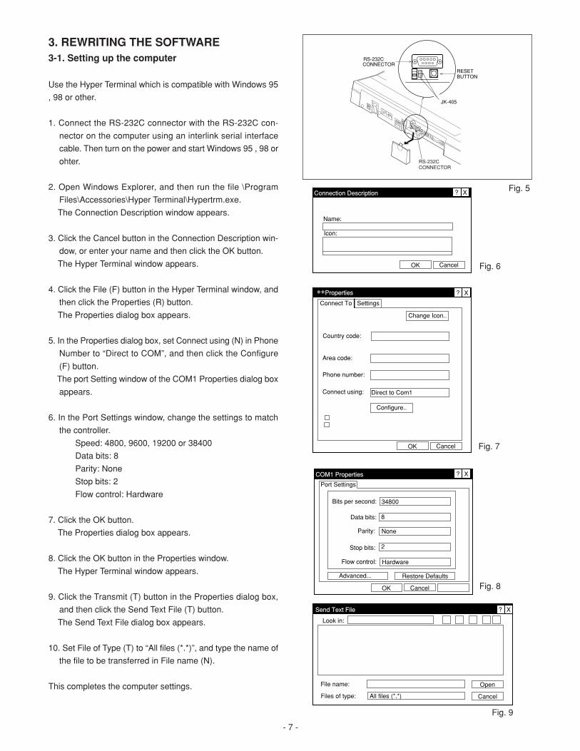
- 7 -
OK Cancel
Connection Description ? X
Name:
Icon:
? X
Change Icon..
Country code:
Area code:
Phone number:
Connect using:
Configure..
OK Cancel
Connect To Settings
Direct to Com1
OK Cancel
COM1 Properties ? X
Bits per second:
Data bits:
Parity:
Stop bits:
Flow control:
Restore DefaultsAdvanced...
Hardware
Port Settings
Open
Send Text File ? X
Look in:
File name:
CancelFiles of type: All files (*.*)
34800
8
None
2
∗∗Properties
3. REWRITING THE SOFTWARE3-1. Setting up the computer
Use the Hyper Terminal which is compatible with Windows 95
, 98 or other.
1. Connect the RS-232C connector with the RS-232C con-
nector on the computer using an interlink serial interface
cable. Then turn on the power and start Windows 95 , 98 or
ohter.
2. Open Windows Explorer, and then run the file \Program
Files\Accessories\Hyper Terminal\Hypertrm.exe.
The Connection Description window appears.
3. Click the Cancel button in the Connection Description win-
dow, or enter your name and then click the OK button.
The Hyper Terminal window appears.
4. Click the File (F) button in the Hyper Terminal window, and
then click the Properties (R) button.
The Properties dialog box appears.
5. In the Properties dialog box, set Connect using (N) in Phone
Number to “Direct to COM”, and then click the Configure
(F) button.
The port Setting window of the COM1 Properties dialog box
appears.
6. In the Port Settings window, change the settings to match
the controller.
Speed: 4800, 9600, 19200 or 38400
Data bits: 8
Parity: None
Stop bits: 2
Flow control: Hardware
7. Click the OK button.
The Properties dialog box appears.
8. Click the OK button in the Properties window.
The Hyper Terminal window appears.
9. Click the Transmit (T) button in the Properties dialog box,
and then click the Send Text File (T) button.
The Send Text File dialog box appears.
10. Set File of Type (T) to “All files (*.*)”, and type the name of
the file to be transferred in File name (N).
This completes the computer settings.
Fig. 5
Fig. 6
Fig. 7
Fig. 8
Fig. 9
RS-232CCONNECTOR
RESET
RS-232CCONNECTOR
JK-405
BUTTON

- 8 -
S A N Y O C o n t r o l l e r - - : - - : - -
C L O C K S E T
[ V 2 . 0 0 ] R E W R I T E ?O K : E N T E R N O : C L R
R E W R I T E P R O G R A M 3 8 4 0 0 8 N 2 H A R D
R E W R I T E P R O G R A M
3-3. Rewriting data
1. Follow the procedure in 3-1. Setting up the computer.
2. Turn on the power or the system controller, and check that
the initial display appears in the LCD. Then press the MENU
button to set to clock setting mode.
3. Press the 0 button and FUNCTION button simultaneously
to set to software rewriting mode.
The current version number appears in the system control-
ler LCD.
Press the CLEAR button if you want to cancel the opera-
tion.
4. Press the ENTER button to set to baud rate setting mode.
The baud rate setting display appears in the system con-
troller LCD.
Press the CLEAR button if you want to cancel the opera-
tion.
5. Press the [+] and [-] buttons to select the baud rate setting.
6. Press the ENTER button to set to software rewrite standby
mode.
The rewrite standby display appears in the system control-
ler LCD.
3-2. Resetting the computer
If an rewriting error occurs, close the Hyper Terminal, and then
repeat the procedure in 3-1. Setting up the computer from step
2.
Speed: 4800, 9600, 19200 or 38400
Data bits: 8
Parity: None
Stop bits: 2
Flow control: Hardware
← (+)BUTTON (–)BUTTON →
Fig. 10
Initial display mode
Software rewriting mode
Baud rate setting mode
Software rewrite standby mode
Clock setting mode
→ 3 8 4 0 0 ↔ 1 9 2 0 0 ↔ 9 6 0 0 ↔ 4 8 0 0←
RS-232CCONNECTOR
RESET
RS-232CCONNECTOR
JK-405
BUTTON

- 9 -
R E W R I T I N G . . .A D D R E S S : 0 0 1 0
R E W R I T E P R O G R A ME R R O R : 3 0
R E W R I T E P R O G R A MC O M P L E T E
S A N Y O C o n t r o l l e r - - : - - : - -
1
RD 2
TD 3
DTR 4
GND 5
DSR 6
RTS 7
CTS 8
9
1
2 RD
3 TD
4 DTR
5 GNG
6 DSR
7 RTS
8 CTS
9
Controller side PC side
7. Click the Open (O) button on the computer screen.
The rewriting display appears in the system controller LCD.
If the software could not be rewritten, an error code appears
in the LCD.
If an error occurs, reset the computer (see “3-2. Resetting
the computer”), and then press the ENTER button and re-
peat the rewriting operation.
Caution:
If an error occurs, do not try to reset the computer by turn-
ing off the system controller power or pressing the RESET
button.
8. When software rewriting is complete, “REWRITE PROGRAM
COMPLETE” appears in the system controller LCD.
Press the ENTER button to the initial display appears in the
LCD.
9. Turn off the power, disconnect the serial cable, and then
install the panel to the rear of the system controller.
Table of error code
3-4. RESET buttonThe following three items can be cleared using the RESET
button.
1. Clock (time)
2. Password code for security lock (cancels the security lock)
3. Status list
Connection Description
COM1 Properties
Open
Send Text File ? X
Look in:
File name:
CancelFiles of type: All files (*.*)
∗∗Properties
Contents
Rewrite mode setting disabled
Access to rewriting prohibition adress
Rewriting operation error
Timeout error when reading
“ : ” Data receiving error
ASCII code data error
Record type error
Checksum error
Data count error
Individual data error
Transfer timeout error
Filename error
Error code
13
14
15
16
20
21
22
23
25
26
27
30
Computer screen
Software rewriting mode
Software rewriting error indication
Software rewriting completion
Wiring diagram for RS-232C interlink serial interface cable
Initial display mode

10
4. PARTS LIST
N.S.P.: Not available as service parts.
CABINET AND CHASSIS PARTS
L8CSB/US
1
2
3
4
4 4
5
6
6
6
6
6
6
6
6
6
7
8
9
11
12
1616
16
1616
1616 16 16
16
16
17 17
17
17
1819
20
21
22
82
23
24 2526
27
2829
303132
33
3435
36 3738
39
4041
424344
45
4647
48 4950
51
5253
545556
57
5859
60 6162
63
6465
666768
69
7071
72 73
74
75 76 77 78 79 80 81
23
2323
13 14
15(N.S.P.)
10
83
8383

11
LOCATION PARTS NO. DESCRIPTION LOCATION PARTS NO. DESCRIPTION
1 645 053 1385 ASSY,CASE2 645 039 9091 BADGE (SANYO)3 645 053 1620 ASSY,TB-24 645 053 1248 SCREW M2*6TP5 645 053 1811 ASSY,LCD6 645 053 1255 SCREW M3*67 645 039 8803 G TERMINAL SCREW M3*108 645 053 1392 REAR PANEL9 645 053 1675 RS232C COVER10 645 039 8926 HOLDER (Include in the ASSY TB-3)11 645 053 1637 ASSY,TB-312 645 053 1835 KEY SW13 613 197 9895 ASSY,KNOB,JOY14 645 053 1668 ZOOM NOB15 645 053 1408 SHIELD CASE (N.S.P.)16 645 039 7752 SCREW M3*10TP17 645 038 5971 CABLE CRAMPER (B)18 645 053 1613 ASSY,TB-119 645 053 1606 ASSY,OP-220 645 053 1590 ASSY,OP-121 645 053 1842 ASSY,CP-122 645 039 8179 COVER,BOTTOM23 645 039 8797 FOOT (T3, DIA10)24 645 039 8278 (REW)25 645 039 8285 (PLAY)26 645 039 8315 (REVERSE)27 645 039 8292 (FF)28 645 039 8322 (STOP)29 645 053 1422 (TRACKING V.LOCK+)30 645 039 8384 (REC/PLAY SPEED UP)31 645 039 8377 (REC/PLAY SPEED DOWN)32 645 053 1415 (TRACKING V.LOCK-)33 645 039 8360 (EJECT)34 645 039 8308 (REC)35 645 039 8339 (STILL)36 645 039 8391 (MULTI)37 645 039 8407 (QUAD)38 645 053 1507 (CAM MPX)39 645 039 8414 (PLUS)40 645 039 8445 (SEQ)41 645 039 8476 (VCR)42 645 053 1521 (EXIT BACK)43 645 039 8490 (NEXT)
44 645 039 8469 (LIVE)45 645 039 8483 (FULL)46 645 053 1514 (MON2 SPOT)47 645 039 8421 (STILL)48 645 039 8186 (ELS)49 645 039 8193 (BLC)50 645 053 1446 (PAN)51 645 039 8209 (AWC SET)52 645 039 8230 (AWC RESET)53 645 053 1453 (TOUR)54 645 053 1484 (AUX)55 645 053 1477 (FOUCUS F)56 645 039 8223 (IRIS+)57 645 053 1460 (FOUCUS N)58 645 039 8216 (IRIS-)59 645 053 1439 (SEQ)60 645 039 8513 (1)61 645 039 8520 (2)62 645 039 8551 (5)63 645 039 8537 (3)64 645 039 8568 (6)65 645 039 8599 (9)66 645 039 8629 (+)67 645 039 8605 (0)68 645 039 8582 (8)69 645 039 8612 (-)70 645 039 8575 (7)71 645 039 8544 (4)72 645 053 1538 (MENU)73 645 053 1491 (AF)74 645 053 1545 (ENTER)75 645 039 8636 (ALARM LIST)76 645 053 1361 (STATUS LIST)77 645 039 8650 (MODE)78 645 039 8667 (INDIVIDUAL)79 645 039 8674 (GROUP)80 645 039 8681 (FUNCTION)81 645 039 8698 (CLEAR)82 645 053 1781 SCREW WITH PLATE M3*10TP83 645 053 1774 NUT(NUT+WASHER+SCREW)
D-SUB CONNECTOR (Included in the ASSY TB-1)

12
Note:1. Materials of Resistors are abbreviated as follows ;
Resistors MT-FILM Metallized Film Resistor MT-GLAZE Metallized Glaze Resistor OXIDE-MT Oxide Metallized Film Resistor
2. CapacitorsUF : µF PF : pF
3. InductorsUH : µH MH : mH
4. N.S.P. : Not available as service parts.
ELECTRICAL PARTS
LOCATION PARTS NO. DESCRIPTION LOCATION PARTS NO. DESCRIPTION
ASSY,OP-1645 053 1590
(DIODES)D1057 645 039 7998 DIODE ALLEY MA153AD1058 645 039 7998 DIODE ALLEY MA153AD1059 645 039 7998 DIODE ALLEY MA153AD1060 645 039 7998 DIODE ALLEY MA153AD1061 645 039 7998 DIODE ALLEY MA153AD1062 645 039 7998 DIODE ALLEY MA153AD1063 645 039 7998 DIODE ALLEY MA153AD1064 645 039 7998 DIODE ALLEY MA153A
(CAPACITORS)C1001 645 039 7547 CERAMIC 0.1UF+80,-20%,50VC1002 645 039 7547 CERAMIC 0.1UF+80,-20%,50VC1003 645 053 1200 CERAMIC 0.01UF+80,-20%,50VC1004 645 053 1200 CERAMIC 0.01UF+80,-20%,50V
(RESISTOR)R1062 645 039 7554 MT-GLAZE 1/8W 0OHM
(MISCELLANEOUS)U1001 645 053 1699 STICK CONTROLER (ALPS)U1002 645 053 1699 STICK CONTROLER (ALPS)CN101 645 039 8902 16P CABLE ASSY (N.S.P.)CN102 645 053 1705 8P CABLE ASSY (N.S.P.)
ASSY,OP-2645 053 1606
(DIODES)D2008 645 053 1934 DIODE ALLEY MA153AD2009 645 053 1934 DIODE ALLEY MA153AD2010 645 053 1934 DIODE ALLEY MA153AD2011 645 053 1934 DIODE ALLEY MA153A
(BUZZER)BZ201 645 053 1903 PIEZO BUZZER
(MISCELLANEOUS)CN201 645 053 1866 9P CABLE ASSY (N.S.P.)CN202 645 053 1859 6P CABLE ASSY (N.S.P.)
ASSY,CP-1645 053 1842
(INTEGRATED CIRCUITS)IC301 645 053 1958 IC,MAX202CSEIC302 410 428 8708 IC,LC87F5064IC303 645 053 1972 IC,PST9127SOT-25IC305 645 053 1965 IC,MAX3082CSAIC306 645 053 1941 IC,AT24C64-10PCIC306 645 053 1989 IC SOCKETIC307 645 053 1927 IC,MN1382-RIC308 645 053 1873 IC,MAX3100EEEIC309 645 053 1880 IC,TC74HC86
(SEMICONDUCTORS)Q3001 645 039 7844 DIGITAL TRANSISTOR DTC114EKAQ3002 645 039 7844 DIGITAL TRANSISTOR DTC114EKAQ3003 645 053 1279 DIGITAL TRANSISTOR DTC144EKQ3004 645 039 7844 DIGITAL TRANSISTOR DTC114EKA
(DIODES)D3001 645 039 7981 DIODE SB10-05PD3002 645 039 7974 DIODE SB05-50PD3003 645 039 7868 DIODE 1SS355D3004 645 039 7868 DIODE 1SS355D3005 645 039 7868 DIODE 1SS355D3006 645 039 7868 DIODE 1SS355D3007 645 039 7974 DIODE SB05-50PD3008 645 039 7868 DIODE 1SS355D3009 645 039 7868 DIODE 1SS355D3010 645 039 7868 DIODE 1SS355D3011 645 039 7868 DIODE 1SS355D3012 645 039 7868 DIODE 1SS355D3013 645 039 7868 DIODE 1SS355D3014 645 039 7868 DIODE 1SS355D3015 645 039 7868 DIODE 1SS355
(INDUCTOR)L3001 645 053 1293 INDUCTOR 100UH
(DC/DC CONVERTER)U3001 645 039 8025 DC/DC CONVERTOR BP5220X
(VARIABLE RESISTORS)VR301 645 039 7820 VR SEMI FIXED 1MOHMVR302 645 039 7837 VR SEMI FIXED 4.7KOHM
(RESONATORS)X3001 645 053 1262 RESONATOR CERAMIC,10MHZX3002 645 040 2135 RESONATOR CRYSTAL,32.768KHZX3003 645 053 1286 RESONATOR CERAMIC,3.68MHZ
(CAPACITORS)C3001 645 039 7509 CERAMIC,100PF+,-5%,50VC3002 645 039 7509 CERAMIC,100PF+,-5%,50VC3003 645 039 7509 CERAMIC,100PF+,-5%,50VC3004 645 039 7509 CERAMIC,100PF+,-5%,50VC3005 645 039 7509 CERAMIC,100PF+,-5%,50VC3006 645 039 7509 CERAMIC,100PF+,-5%,50VC3007 645 039 7509 CERAMIC,100PF+,-5%,50VC3008 645 039 7509 CERAMIC,100PF+,-5%,50VC3009 645 039 7547 CERAMIC,0.1UF+80,-20%,50VC3010 645 039 7547 CERAMIC,0.1UF+80,-20%,50VC3011 645 039 7547 CERAMIC,0.1UF+80,-20%,50VC3012 645 039 7547 CERAMIC,0.1UF+80,-20%,50VC3013 645 039 7547 CERAMIC,0.1UF+80,-20%,50VC3014 645 039 7523 CERAMIC,15PF+,-5%,50VC3015 645 039 7523 CERAMIC,15PF+,-5%,50VC3016 645 039 7547 CERAMIC,0.1UF+80,-20%,50VC3017 645 039 7530 CERAMIC,20PF+,-5%,50VC3021 645 039 7547 CERAMIC,0.1UF+80,-20%,50VC3022 645 039 7547 CERAMIC,0.1UF+80,-20%,50VC3023 645 039 7547 CERAMIC,0.1UF+80,-20%,50VC3024 645 039 7547 CERAMIC,0.1UF+80,-20%,50VC3025 645 039 7479 ELECTRIC,1000UF,+,-20%,50VC3026 645 039 7486 ELECTRIC,47UF,+,-20%,50VC3027 645 039 7486 ELECTRIC,47UF,+,-20%,50VC3028 645 039 7493 ELECTRIC,470UF,+,-20%,25VC3029 645 039 7462 ELECTRIC,10UF,+,-20%,16VC3030 645 039 7462 ELECTRIC,10UF,+,-20%,16VC3031 645 039 7462 ELECTRIC,10UF,+,-20%,16VC3032 645 039 7462 ELECTRIC,10UF,+,-20%,16VC3033 645 039 7486 ELECTRIC,47UF,+,-20%,50VC3034 645 039 7448 ELECTRIC,1UF,+,-20%,50VC3035 645 039 7462 ELECTRIC,10UF,+,-20%,16VC3036 645 039 7486 ELECTRIC,47UF,+,-20%,50V

13
LOCATION PARTS NO. DESCRIPTION LOCATION PARTS NO. DESCRIPTION
CN305 645 039 7912 6P CONNECTOR (N.S.P.)CN306 645 039 7905 3P CONNECTOR (N.S.P.)CN307 645 053 1828 2P CONNECTOR (N.S.P.)
ASSY,TB-1645 053 1613
(SWITCHES)S4001 645 039 8001 DIP SWS4002 645 053 1354 TACT SWS4003 645 053 1309 SLIDE SWS4004 645 039 8094 S POWER SW
(JACKS/TERMINAL)JK401 645 039 7721 DC JACKJK402 645 031 6913 MODULAR JACKJK403 645 031 6913 MODULAR JACKJK404 645 039 8070 PUSH LOCK TERMINAL(2P)JK405 645 039 8100 TEST PIN
(FILTERS)F4001 645 039 7806 EMI FILTORF4002 645 039 7806 EMI FILTORF4003 645 039 7806 EMI FILTORF4004 645 039 7813 EMI FILTOR
(INDUCTORS)L4001 645 039 7790 INDUCTOR,0.47UHL4002 645 039 7790 INDUCTOR,0.47UH
(CAPACITORS)C4001 645 039 7516 CERAMIC 0.01UF+80,-20%,50VC4002 645 039 7516 CERAMIC 0.01UF+80,-20%,50V
(DIODES)D4001 645 053 1347 ZENNER DIODED4002 645 053 1347 ZENNER DIODED4003 645 053 1347 ZENNER DIODED4004 645 053 1347 ZENNER DIODE
(RESISTORS)R4001 645 039 7608 MT-GLAZE 1/8W 120OHM+,-0.5%R4002 645 039 7554 MT-GLAZE 1/8W 0OHMR4003 645 039 7554 MT-GLAZE 1/8W 0OHMR4004 645 039 7554 MT-GLAZE 1/8W 0OHMR4005 645 039 7554 MT-GLAZE 1/8W 0OHMR4006 645 039 7554 MT-GLAZE 1/8W 0OHMR4008 645 039 7554 MT-GLAZE 1/8W 0OHMR4009 645 039 7554 MT-GLAZE 1/8W 0OHMR4010 645 039 7554 MT-GLAZE 1/8W 0OHMR4011 645 039 7554 MT-GLAZE 1/8W 0OHM
(MISCELLANEOUS)645 053 1774 NUT(NUT+WASHER+SCREW)
D-SUB CONNECTORCN403 645 039 8087 CONNECTOR (9P) D-SUBCN401 645 039 8872 6P CABLE ASSY (N.S.P.)CN402 645 039 8896 9P CABLE ASSY (N.S.P.)
ASSY,TB-2645 053 1620
(LED)D5001 645 039 7882 LED(GREEN)D5002 645 039 7875 LED(RED)
(MISCELLANEOUS)CN501 645 039 8865 3P CABLE ASSY (N.S.P.)
ASSY,TB-3645 053 1637 ASSY,TB-3
(BATTERY)Z6001 645 039 8063 BATTERY
(MISCELLANEOUS)CN601 645 039 7936 CONNECTOR(2P) (N.S.P.)
645 039 8926 HOLDER
C3037 645 039 7462 ELECTRIC,10UF,+,-20%,16VC3038 645 039 7455 ELECTRIC,100UF,+,-20%,6.3VC3039 645 039 7547 CERAMIC 0.1UF+80,-20%,50VC3040 645 039 7516 CERAMIC 0.01UF+80,-20%,50VC3041 645 039 7516 CERAMIC 0.01UF+80,-20%,50VC3042 645 039 7516 CERAMIC 0.01UF+80,-20%,50VC3046 645 039 7547 CERAMIC 0.1UF+80,-20%,50VC3047 645 053 1194 CERAMIC 0.01UF+,-20%,50V
(RESISTORS)R3001 645 039 7646 MT-GLAZE 1/8W 33KOHM+,-0.5%R3002 645 039 7646 MT-GLAZE 1/8W 33KOHM+,-0.5%R3003 645 039 7646 MT-GLAZE 1/8W 33KOHM+,-0.5%R3004 645 039 7646 MT-GLAZE 1/8W 33KOHM+,-0.5%R3005 645 039 7646 MT-GLAZE 1/8W 33KOHM+,-0.5%R3006 645 039 7646 MT-GLAZE 1/8W 33KOHM+,-0.5%R3007 645 039 7646 MT-GLAZE 1/8W 33KOHM+,-0.5%R3008 645 039 7646 MT-GLAZE 1/8W 33KOHM+,-0.5%R3009 645 039 7691 MT-GLAZE 1/8W 560OHM+,-0.5%R3010 645 039 7585 MT-GLAZE 1/8W 10KOHM+,-0.5%R3011 645 039 7684 MT-GLAZE 1/8W 470KOHM+,-0.5%R3012 645 039 7592 MT-GLAZE 1/8W 10MOHM+,-0.5%R3013 645 039 7653 MT-GLAZE 1/8W 330KOHM+,-0.5%R3014 645 039 7677 MT-GLAZE 1/8W 4.7KOHM+,-0.5%R3015 645 039 7585 MT-GLAZE 1/8W 10KOHM+,-0.5%R3017 645 039 7578 MT-GLAZE 1/8W 1KOHM+,-0.5%R3018 645 039 7615 MT-GLAZE 1/8W 1.5KOHM+,-0.5%R3020 645 039 7585 MT-GLAZE 1/8W 10KOHM+,-0.5%R3022 645 039 7585 MT-GLAZE 1/8W 10KOHM+,-0.5%R3025 645 039 7691 MT-GLAZE 1/8W 560OHM+,-0.5%R3026 645 039 7691 MT-GLAZE 1/8W 560OHM+,-0.5%R3028 645 039 7615 MT-GLAZE 1/8W 1.5KOHM+,-0.5%R3029 645 039 7615 MT-GLAZE 1/8W 1.5KOHM+,-0.5%R3030 645 039 7660 MT-GLAZE 1/8W 390OHM+,-0.5%R3031 645 039 7707 MT-GLAZE 1/8W 68OHM+,-0.5%R3032 645 039 7707 MT-GLAZE 1/8W 68OHM+,-0.5%R3033 645 039 7561 MT-GLAZE 1/8W 100OHM+,-0.5%R3034 645 039 7585 MT-GLAZE 1/8W 10KOHM+,-0.5%R3035 645 039 7585 MT-GLAZE 1/8W 10KOHM+,-0.5%R3036 645 039 7639 MT-GLAZE 1/8W 270KOHM+,-0.5%R3037 645 053 1217 MT-GLAZE 1/8W 4.3KOHM+,-0.5%R3041 645 039 7554 MT-GLAZE 1/8W 0OHMR3042 645 039 7554 MT-GLAZE 1/8W 0OHMR3043 645 039 7554 MT-GLAZE 1/8W 0OHMR3053 645 039 7578 MT-GLAZE 1/8W 1KOHM+,-0.5%R3054 645 039 7578 MT-GLAZE 1/8W 1KOHM+,-0.5%R3055 645 039 7578 MT-GLAZE 1/8W 1KOHM+,-0.5%R3056 645 039 7578 MT-GLAZE 1/8W 1KOHM+,-0.5%R3057 645 039 7578 MT-GLAZE 1/8W 1KOHM+,-0.5%R3058 645 039 7578 MT-GLAZE 1/8W 1KOHM+,-0.5%R3059 645 039 7578 MT-GLAZE 1/8W 1KOHM+,-0.5%R3060 645 039 7578 MT-GLAZE 1/8W 1KOHM+,-0.5%R3064 645 039 7585 MT-GLAZE 1/8W 10KOHM+,-0.5%R3065 645 039 7585 MT-GLAZE 1/8W 10KOHM+,-0.5%R3066 645 039 7585 MT-GLAZE 1/8W 10KOHM+,-0.5%R3067 645 039 7585 MT-GLAZE 1/8W 10KOHM+,-0.5%R3068 645 039 7585 MT-GLAZE 1/8W 10KOHM+,-0.5%R3069 645 039 7585 MT-GLAZE 1/8W 10KOHM+,-0.5%R3070 645 039 7585 MT-GLAZE 1/8W 10KOHM+,-0.5%R3071 645 039 7585 MT-GLAZE 1/8W 10KOHM+,-0.5%R3072 645 039 7554 MT-GLAZE 1/8W 0OHMR3074 645 039 7554 MT-GLAZE 1/8W 0OHMR3080 645 039 7554 MT-GLAZE 1/8W 0OHMR3081 645 039 7554 MT-GLAZE 1/8W 0OHMR3082 645 039 7554 MT-GLAZE 1/8W 0OHMR3084 645 039 7578 MT-GLAZE 1/8W 1KOHM+,-0.5%R3085 645 039 7585 MT-GLAZE 1/8W 10KOHM+,-0.5%R3086 645 039 7578 MT-GLAZE 1/8W 1KOHM+,-0.5%R3087 645 053 1224 MT-GLAZE 1/8W 470KOHM+,-0.5%R3089 645 039 7578 MT-GLAZE 1/8W 1KOHM+,-0.5%R3090 645 039 7578 MT-GLAZE 1/8W 1KOHM+,-0.5%R3091 645 039 7585 MT-GLAZE 1/8W 10KOHM+,-0.5%
(MISCELLANEOUS)CN301 645 039 7950 16P CONNECTOR (N.S.P.)CN302 645 039 7950 16P CONNECTOR (N.S.P.)CN303 645 053 1323 9P CONNECTOR (N.S.P.)CN304 645 039 7929 9P CONNECTOR (N.S.P.)CN308 645 053 1316 8P CONNECTOR (N.S.P.)

14
ASSY,LCD645 053 1811
(LCD)629 016 4750 LCD DM1623-7BL3(MISCELLANEOUS)645 039 8919 16P CABLE ASSY
ACCESSORIES & PACKING MATERIALS613 196 5065 INSTRUCTION MANUAL(U.S.A. & CANADA)613 196 5058 INSTRUCTION MANUAL(EUROPE)645 039 8940 AC ADAPTOR (U.S.A. & CANADA)645 039 8957 AC ADAPTOR (EUROPE.)645 053 1712 MODULAR CABLE645 053 1729 PACKING CASE645 038 6046 POLY BAG
LOCATION PARTS NO. DESCRIPTION

C1
CIRCUIT DIAGRAMS & PRINTED WIRING BOARDS
TABLE OF CONTENTS
1. OVERALL WIRING AND CIRCUIT DIAGRAMSOVERALL WIRING ........................................................................................................................................... C2
TB-1 BOARD ..................................................................................................................................................... C2
CP-1 BOARD .................................................................................................................................................... C3
OP-1 BOARD .................................................................................................................................................... C4
OP-2 BOARD .................................................................................................................................................... C5
TB-2 BOARD ..................................................................................................................................................... C5
TB-3 BOARD ..................................................................................................................................................... C5
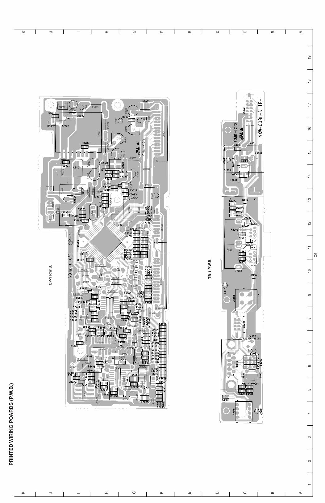
2. PRINTED WIRING BOARDS (P.W.B.)CP-1 P.W.B. ...................................................................................................................................................... C6
TB-1 P.W.B. ...................................................................................................................................................... C6
OP-1 P.W.B. ...................................................................................................................................................... C7
OP-2 P.W.B. ...................................................................................................................................................... C7
TB-2 P.W.B. ...................................................................................................................................................... C7
TB-3 P.W.B. ...................................................................................................................................................... C7
PRODUCT SAFETY NOTICETHE COMPONENTS DESIGNATED BY A SYMBOL ( ) IN THISSCHEMATIC DIAGRAM DESIGNATES COMPONENTS WHOSEVALUE ARE OF SPECIAL SIGNIFICANCE TO PRODUCT SAFETY.SHOULD ANY COMPONENT DESIGNATED BY A SYMBOL NEED TOBE REPLACED, USE ONLY THE PART DESIGNATED IN THE PARTSLIST.DO NOT DEVIATE FROM THE RESISTANCE, WATTAGE AND VOLT-AGE RATINGS SHOWN.

ABCDEFGHIJK
12
34
56
78
910
1112
1314
1516
1718
19
ABCDEFGHIJK
C2
OV
ER
AL
L W
IRU
NG
& B
LO
CK
DIA
GR
AM
SO
VE
RA
LL
WIR
ING
TB
-1 B
OA
RD

ABCDEFGHIJK
12
34
56
78
910
1112
1314
1516
1718
19
ABCDEFGHIJK
C3
CP
-1 B
OA
RD

ABCDEFGHIJK
12
34
56
78
910
1112
1314
1516
1718
19
ABCDEFGHIJK
C4
OP
-1 B
OA
RD

ABCDEFGHIJK
12
34
56
78
910
1112
1314
1516
1718
19
ABCDEFGHIJK
C5
OP
-2 B
OA
RD
TB
-3 B
OA
RD
TB
-2 B
OA
RD
ABCDEFGHIJK
12
34
56
78
910
1112
1314
1516
1718
19
ABCDEFGHIJK
C6
PR
INT
ED
WIR
ING
PO
AR
DS
(P.
W.B
.)
CP
-1 P
.W.B
.
TB
-1 P
.W.B
.
JP30
47
C30
48
JP30
46
C30
29
JP3045
C3031JP3041
CN302
-
-
-
-
IC30
6
1
JP30
48C
3032
JP3044
C3030
JP3042
1 6
CN3081 8
JP3043
X30
03
JP3040
JP3038
JP3036
JP30
37
JP30
39
1
1
13
CN
309
JP30
34
JP3032
JP3033
JP3031JP3032
JP3030JP3029
JP3026
JP3023
JP3019
JP3027
JP3024
JP3018
JP3016
JP3028
JP3025
JP3022
JP3020
JP3017
JP3015
JP30
21
CN
302
116
CN
303
19
TP30
4
1
JP3013
C30
34
-
X30
02
X30
01
JP30
14
JP30
11
-C
3033
TP30
2JP30
08
JP30
06
C30
25
-
JP3010
JP3006
JP3005
JP3007
-
-
--
C30
37
C30
26C
3027
C30
25
CN
301
161
TP30
2
TP30
5
C30
36V
R30
2
TP30
1
VR
301
-
JP30
04JP
3003
JP3001
-
CN307
3 1
TP30
3
C3038
U30
01
CN
304
JP30
12
C30
28
-
91

ABCDEFGHIJK
12
34
56
78
910
1112
1314
1516
1718
19
ABCDEFGHIJK
C7
S10
01S
1002
S10
03
S10
04S
1005
S10
06
S10
07S
1008
S10
09
S10
10S
1011
S10
12
S10
13S
1014
S10
15
S10
16S
1017
S10
18
S10
20S
1021
S10
22
S10
23S
1024
S10
25
S10
28S
1029
S10
30
S10
31S
1032
S10
33
S10
34S
1035
S10
36
S10
37S
1038
S10
39
S10
40S
1041
S10
42
S10
43S
1045
S10
46
S10
48S
1049
S10
50
S10
51S
1052
S10
53S
1019
S10
47S
1027
CN
102
CN
101
JP10
28
JP10
26JP10
27
JP10
25
JP10
24
JP10
22
JP10
23
JP1019
JP1017
JP1021
JP1020 JP1018
JP1016
JP1015
JP1013JP1014
JP1011
JP1009
JP1012 JP1010
JP1007
JP1006
JP1008
JP1005
JP1003
JP1002
JP1004
JP1001
OP
-1 P
.W.B
.
OP
-2 P
.W.B
.
TB
-2 P
.W.B
.
TB
-3 P
.W.B
.

Apr./’02 Printed in Japan
SANYO Electric Co., Ltd.Osaka, Japan