sembodai rukmani varatharajan engineering · pdf fileto construct the r, rc &ujt...
TRANSCRIPT

R Dhinesh kumar,M.E/AP/EEE Page 1
SEMBODAI RUKMANI VARATHARAJAN ENGINEERING COLLEGE,
SEMBODAI, NAGAPATTINAM.
DEPARTMENT OF ELECTRICAL AND ELECTRONICS ENGINEERING
VI- Semester – B.E (EEE)
EE6611 POWER ELECTRONICS AND DRIVES LABORATORY
Prepared by,
Mr.R.Dhinesh kumar M.E., AP/EEE

R Dhinesh kumar,M.E/AP/EEE Page 2
CONTENTS
S.N
O DATE NAME OF THE EXPERIMENT
PAGE
NO
MAR
KS
SIGN
1 Gate Pulse Generation using R,RC and UJT
2 Characteristics of SCR and Triac
3 Characteristics of MOSFET and IGBT
4 AC to DC half controlled converter
5 AC to DC fully controlled Converter
6 Step down and step up MOSFET based choppers
7 IGBT based single phase PWM inverter
8 IGBT based three phase PWM inverter
9 AC Voltage controller
10 Switched mode power converter.
11 SimulationofPEcircuits(1Φ&3Φsemiconverter,1Φ&3Φfullcon
verter,dc-dc converters, ac voltage controllers).

R Dhinesh kumar,M.E/AP/EEE Page 3
INSTRUCTIONS TO THE STUDENTS
1. Candidates should come to the lab with proper uniform and good quality
leather shoes.
2. Punctuality and strict Discipline should be maintained.
3. Study and prepare well before entering into the lab.
4. Complete the observation after completion of the experiment in the lab
itself.
5. Be alert till the experiment is completed.
6. Make sure that the supply is OFF before touching any terminals.
7. Use proper rating equipments carefully, for which you are duly responsible.
8. Handle the equipments carefully, for which you are duly responsible.
9. Return all the components and make sure that nothing is left on the
worktable.
10. In case of any wrong observations you have to switch off the power supply
related with it.
11. Make series circuit connections before the parallel circuit like voltmeter
connections.
12. Don’t use meter terminals as junctions and place them to read conveniently.
13. Check the rheostat positions and connections whether they have been
connected properly or not.
R Dhinesh kumar,M.E/AP/EEE Page 4
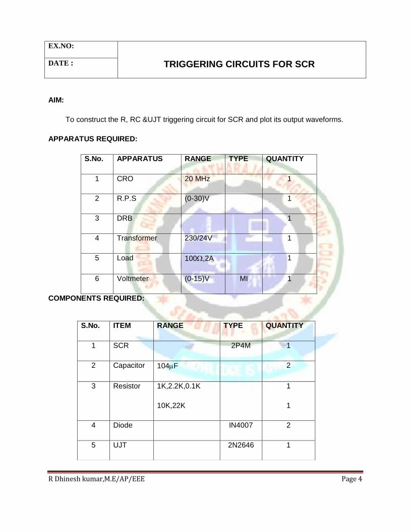
EX.NO:
TRIGGERING CIRCUITS FOR SCR DATE :
AIM:
To construct the R, RC &UJT triggering circuit for SCR and plot its output waveforms.
APPARATUS REQUIRED:
S.No. APPARATUS RANGE TYPE QUANTITY
1 CRO 20 MHz 1
2 R.P.S (0-30)V 1
3 DRB 1
4 Transformer 230/24V 1
5 Load 100,2A 1
6 Voltmeter (0-15)V MI 1
COMPONENTS REQUIRED:
S.No. ITEM RANGE TYPE QUANTITY
1 SCR 2P4M 1
2 Capacitor 104F 2
3 Resistor 1K,2.2K,0.1K
10K,22K
1
1
4 Diode IN4007 2
5 UJT 2N2646 1

R Dhinesh kumar,M.E/AP/EEE Page 5
PROCEDURE: (R-TRIGGERING)
1. Make the connections as per the circuit diagram.
2. Vary the DRB to get maximum resistance value.
3. Switch on the power supply
4. Note down the output waveform across the load and the voltage across gate
cathode using a CRO.
5. Repeat the procedure for various resistor values of potentiometer.
6. Switch off the power and remove the connections.
CIRCUIT DIAGRAM (RESISTANCE FIRING CIRCUIT) :
LOAD
V
O
VS D
R
R2
R1
CRO
I
50/5A
R Dhinesh kumar,M.E/AP/EEE Page 6
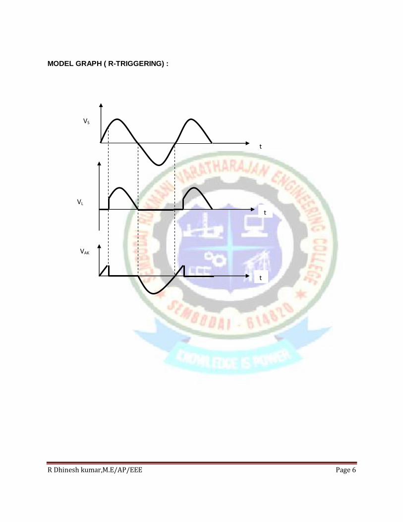
MODEL GRAPH ( R-TRIGGERING) :
VS
VL
VAK
t
t
t
R Dhinesh kumar,M.E/AP/EEE Page 7
TABULAR COLUMN (R-TRIGGERING) :
S.No.
Input
Voltage
(V)
Input Cycle
Time
(Ms)
Resistance
Value
(K Ω )
O/P
Voltage
V rms (V)
Voltage
Across
(Anode- Cathode)
V rms (V)
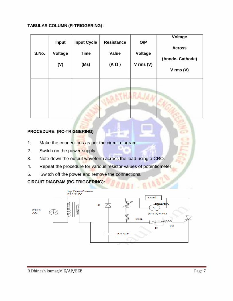
PROCEDURE: (RC-TRIGGERING)
1. Make the connections as per the circuit diagram.
2. Switch on the power supply.
3. Note down the output waveform across the load using a CRO.
4. Repeat the procedure for various resistor values of potentiometer.
5. Switch off the power and remove the connections.
CIRCUIT DIAGRAM (RC-TRIGGERING):
R Dhinesh kumar,M.E/AP/EEE Page 8
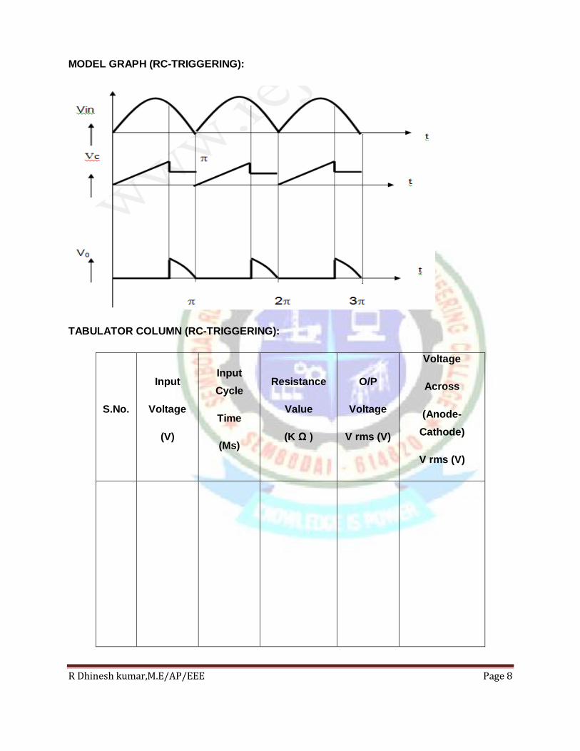
MODEL GRAPH (RC-TRIGGERING):
TABULATOR COLUMN (RC-TRIGGERING):
S.No.
Input
Voltage
(V)
Input
Cycle
Time
(Ms)
Resistance
Value
(K Ω )
O/P
Voltage
V rms (V)
Voltage
Across
(Anode-
Cathode)
V rms (V)
R Dhinesh kumar,M.E/AP/EEE Page 9
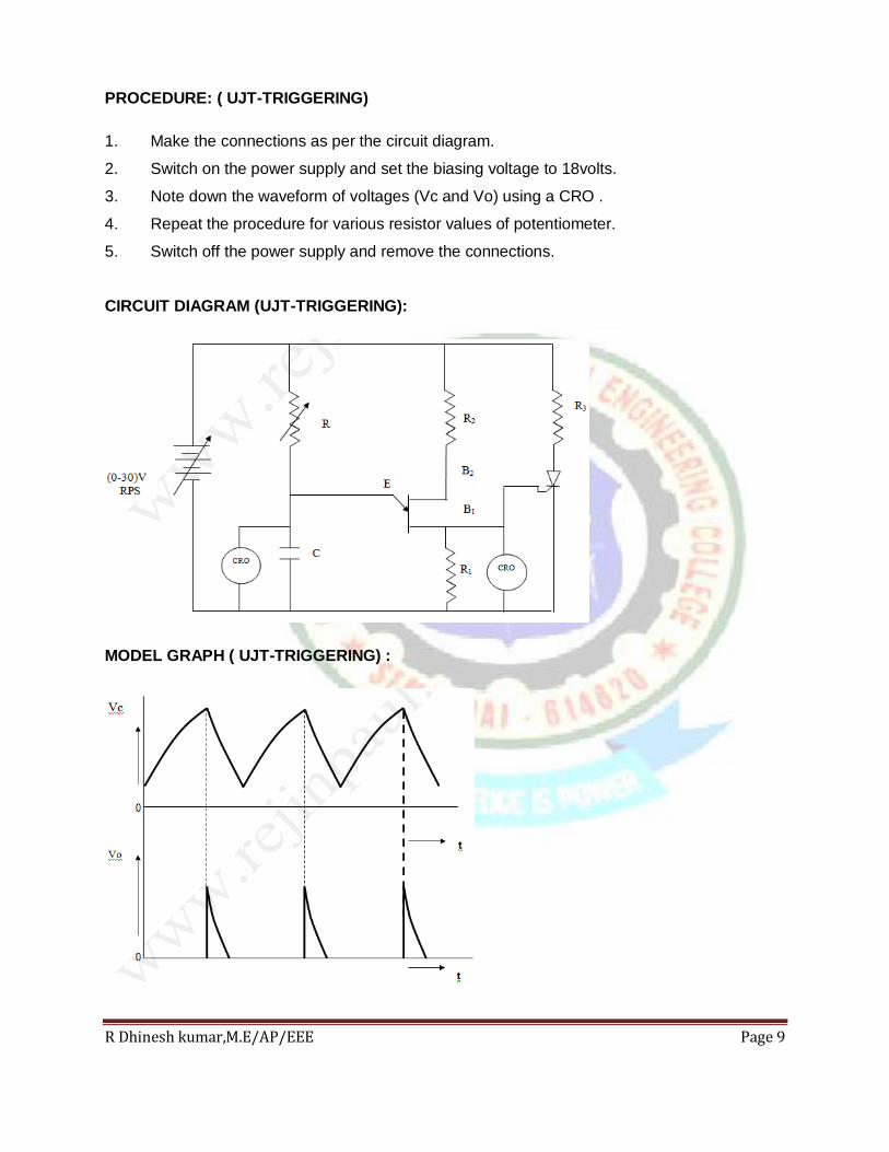
PROCEDURE: ( UJT-TRIGGERING)
1. Make the connections as per the circuit diagram.
2. Switch on the power supply and set the biasing voltage to 18volts.
3. Note down the waveform of voltages (Vc and Vo) using a CRO .
4. Repeat the procedure for various resistor values of potentiometer.
5. Switch off the power supply and remove the connections.
CIRCUIT DIAGRAM (UJT-TRIGGERING):
MODEL GRAPH ( UJT-TRIGGERING) :

R Dhinesh kumar,M.E/AP/EEE Page 10
TABULAR COLUMN (UJT-TRIGGERING):
S.No.
Resistor
value(r)
(ω)
Capacitor
voltage
Vc (v)
Charging
time
(ms)
Discharging
Time
(ms)
Voltage
vo
(v)
Time
Period
(ms)

R Dhinesh kumar,M.E/AP/EEE Page 11
VIVA QUESTIONS: -
1. What is the meaning of triggering?
2. List the different types of triggering methods.
3. Why gate triggering is preferred than other types?
4. Explain how the firing angle will be extended more than 90 by using RC triggering.
5. Why UJT triggering is superior than R and RC triggering?
RESULT:

R Dhinesh kumar,M.E/AP/EEE Page 12
EX.NO:
CHARACTERISTICS OF SCR AND TRIAC DATE :
A.CHARACTERISTICS OF SCR
AIM:
To obtain the V-I characteristics of SCR(Silicon Controlled Rectifier) and to measure the
breakdown voltage and holding current values .
APPARATUS REQUIRED:
S.No. APPARATUS RANGE TYPE QUANTITY
1 SCR 1
2 Regulated Power Supply (0-30) V 1
3 Voltmeter (0-30) V MC 1
4 Ammeter (0-30)mA MC 1
5 Ammeter (0-100)μA MC 1
6 Resistor 1 kΩ 1
THEORY:
An SCR is a Three terminal ,four layer latching device.The three terminals are
anode,cathode and gate.When the anode is more positive w.r.t the cathode,junctions j1,j3 are
forward biased and the junction j2 is reverse biased.Only a small leakage current flows through
the device. The device is said to be in the forward blocking state or OFF state.When the anode to
cathode voltage is increased to break over value, the junction j2 breaks down and device starts
conducting.The anode current must be more than a value known as latching current in order to
maintain the device in the ON state. Once SCR starts conducting, it behaves like a conducting
diode and gate has no control over the device. The device can be turned OFF only by bringing
the device current below a value known as holding current . The forward voltage drop across the
R Dhinesh kumar,M.E/AP/EEE Page 13
device in the ON state is around one volt. When yhe cathode voltage is made positive w.r .t the
anode voltage the junction j2 is forward biased and the junction’s j1 and j3 are reverse biased.
The device will be in the reverse blocking state and small reverse leakage current flows through
device.The device can be turned ON at forward voltage voltage less than break over voltage by
applying suitable gate current.
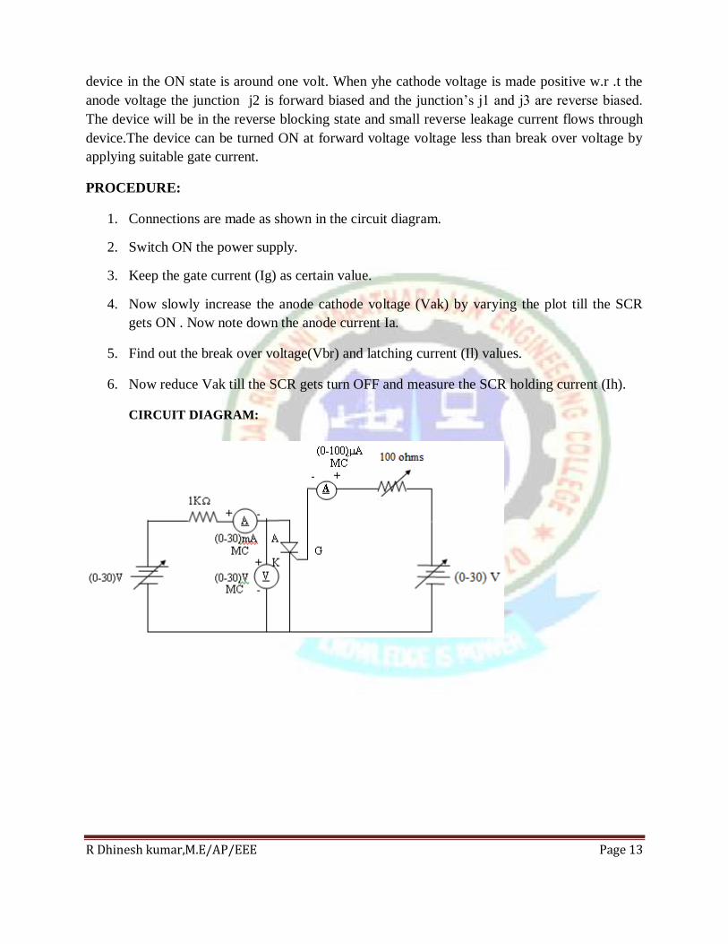
PROCEDURE:
1. Connections are made as shown in the circuit diagram.
2. Switch ON the power supply.
3. Keep the gate current (Ig) as certain value.
4. Now slowly increase the anode cathode voltage (Vak) by varying the plot till the SCR
gets ON . Now note down the anode current Ia.
5. Find out the break over voltage(Vbr) and latching current (Il) values.
6. Now reduce Vak till the SCR gets turn OFF and measure the SCR holding current (Ih).
CIRCUIT DIAGRAM:

R Dhinesh kumar,M.E/AP/EEE Page 14
TABULAR COLUMN:
S.No.
IG =….(μA) IG =….(μA)
VAK (V) IA (mA) VAK (V) IA (mA)
MODEL GRAPH:
I g1
I g2
ig2 >ig1
IA
VAK
K A G
ZP4M

R Dhinesh kumar,M.E/AP/EEE Page 15
RESULT:
Thus the forward VI Charcteristics of SCR have been determined experimentally.

R Dhinesh kumar,M.E/AP/EEE Page 16
B.CHARACTERISTICS OF TRIAC
AIM:
To obtain the VI Characteristics of TRIAC.
APPARATUS REQUIRED:
S.NO NAME RANGE TYPE QUANTITY
1 TRIAC - BT136 1
2 RPS (0-30)V - 2
3 Ammeter (0-50)Ma MC 2
4 Voltmeter (0-30)v MC 1
5 Resistor 1.2 kΩ - 2
6 Bread board 1
7 Connecting wires As per requirements
THEORY:
A TRIAC is a bidirectional thyristor(it can conduct in both directions) with three terminals. It
is used extensively for control of power in AC circuit. When in operation ,a TRIAC is equivalent to SCRs
connected in anti parallel. Its three terminals are usually designated as MT1,MT2 and gate.
The V-I characteristics of a TRIAC is biased on the terminal MT1 as the reference point .The
first quadrant is the region wherein MT2 is positive w.r.t MT1 and vice versa for the third quadrant.The
peak voltage applied across the device in either direction must be less the break over voltage in order to
retain control by the gate. A gate current of specified amplitude of either polarity will trigger the TRIAC
into conduction in either quadrant, assuming that the device is in a blocking condition initially before the
gate signal is applied. The characteristics of a TRIAC are similar to those of an SCR ,both in blocking and
conducting states,except for the fact that SCR conduct only in the forward direction, whereas the TRIAC
conducts in both the directions.
R Dhinesh kumar,M.E/AP/EEE Page 17
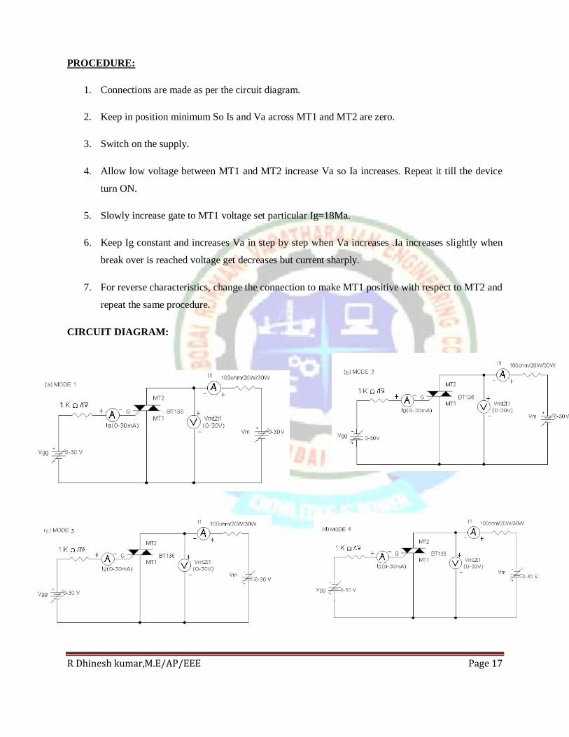
PROCEDURE:
1. Connections are made as per the circuit diagram.
2. Keep in position minimum So Is and Va across MT1 and MT2 are zero.
3. Switch on the supply.
4. Allow low voltage between MT1 and MT2 increase Va so Ia increases. Repeat it till the device
turn ON.
5. Slowly increase gate to MT1 voltage set particular Ig=18Ma.
6. Keep Ig constant and increases Va in step by step when Va increases .Ia increases slightly when
break over is reached voltage get decreases but current sharply.
7. For reverse characteristics, change the connection to make MT1 positive with respect to MT2 and
repeat the same procedure.
CIRCUIT DIAGRAM:

R Dhinesh kumar,M.E/AP/EEE Page 18
MODEL GRAPH:
TABULATION:
S.No.
MODE-1 MODE-2 MODE-3 MODE-4
IG =….(mA) IG=….(mA) IG=….(mA) IG=….(mA)
VAK (V) IA (mA) VAK (V) IA (mA) VAK (V) IA (mA) VAK (V) IA (mA)

R Dhinesh kumar,M.E/AP/EEE Page 19
VIVA QUESTION:
1. What is TRIAC?
2. TRIAC is only used in AC circuits .Justify.
3. How does a TRIAC work?
4. Draw the equivalent circuit for TRIAC?
5. What are the difference between SCR and TRIAC?
RESULT:
Thus the Characteristics of TRIAC was obtained.

R Dhinesh kumar,M.E/AP/EEE Page 20
EX.NO:
CHARACTERISTICS OF MOSFET AND IGBT DATE :
A. CHARACTERISTICS OF MOSFET
AIM
To determine the characteristics of MOSFET & IGBT.
APPARATUS REQUIRED:
S.NO NAME RANGE TYPE QUANTITY
1 MOSFET - IRFP 350 1
2 Voltmeter (0-30)v MC 2
3 Ammeter (0-15)mA MC 1
4 Resistor 1kΩ - 2
5 RPS (0-30)v - 2
6 Bread board 1
7 Connecting Wires As per
requirements
THEORY:
MOSFET
a)output characteristics:
It indicate the variation of drain current Id as a function of drain –source voltage Vgs as
aparameter. For low values of Vds, the graph between Id-vds is almost linear, this indicates a
constant value of an resistance Rds=Vds/Id. For given Vgs is increased , output characteristic is
relatively flat indicating that drain current is nearly constant.
b)Transfer characteristics:
This characteristic shows the variation of drain current Id as a function of gate
source voltage Vgs.Thershold voltage Vgst is an important parameter of MOSFET.Vgst is the
minimum positive voltage between gate and source to induce n- channel. Thus , for threshold
voltage below Vgst ,device is in the OFF state .Magnitude of Vgst is of the order of 2 to 3v.
R Dhinesh kumar,M.E/AP/EEE Page 21
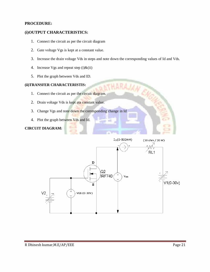
PROCEDURE:
(i)OUTPUT CHARACTERISTICS:
1. Connect the circuit as per the circuit diagram
2. Gate voltage Vgs is kept at a constant value.
3. Increase the drain voltage Vds in steps and note down the corresponding values of Id and Vds.
4. Increase Vgs and repeat step (i)&(ii)
5. Plot the graph between Vds and ID.
(ii)TRANSFER CHARACTERISTIS:
1. Connect the circuit as per the circuit diagram.
2. Drain voltage Vds is kept ata constant value.
3. Change Vgs and note down the corresponding change in Id
4. Plot the graph between Vds and Id.
CIRCUIT DIAGRAM:
R Dhinesh kumar,M.E/AP/EEE Page 22
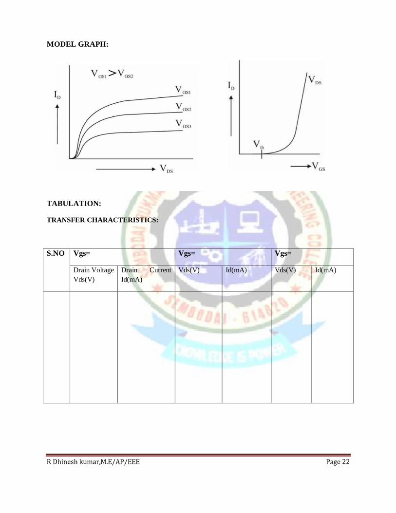
MODEL GRAPH:
TABULATION:
TRANSFER CHARACTERISTICS:
S.NO Vgs= Vgs= Vgs=
Drain Voltage
Vds(V)
Drain Current
Id(mA)
Vds(V) Id(mA) Vds(V) Id(mA)

R Dhinesh kumar,M.E/AP/EEE Page 23
DRAIN CHARACTERISTICS:
S.NO Gate Voltage Vgs(V) Drain Current Id(mA)
VIVA QUESTION:
1. What are the different types of power MOSFET?
2. Power MOSFET is a voltage controlled device?Why?
3. Name the three regions of operation in a MOSFET.
4. Define threshold voltage.
5. Define Pinch off voltage.
RESULT:
Thus the output characteristics and transfer characteristics of given MOSFET was obtained.

R Dhinesh kumar,M.E/AP/EEE Page 24
B.CHARACTERISTICS OF IGBT
AIM:
To obtain the output characteristics and transfer characteristics of IGBT
APPARATUA REQUIRED:
S.NO NAME RANGE TYPE QUANTITY
1 IGBT Kit - BT126 1
2 Voltmeter (0-30)V MC 2
3 Ammeter (0-15)A MC,MA 1
4 Patch cards As per require
5 Resistor 1KΩ - 2
6 Bread board 1
7 Connecting Wires As per require
THEORY:
a)output characteristics:
output characteristics of an IGBT show the plot of collector current Ic versus collector-Emitter
voltages. In the forward direction ,the shape of the output characteristics is similar to that of BJT. But
here the controlling parameter is Gate-Emitter voltage Vge because IGBT is a voltage controlled device.
When the device is OFF , junction j2 blocks forward voltage and in case reverse voltage appears across
collector and emitter,junction j1 blocks it. Vrm is the maximum reverse breakdown voltage.
b)Transfer characteristics:
The transfer characteristics of an IGBT is a plot of collector current Ic versus Gate emitter voltage
Vge. This characteristic is identical to that of power MOSFET .when Vge is less than the threshold
voltage Vget,IGBT is in the OFF State.

R Dhinesh kumar,M.E/AP/EEE Page 25
PROCEDURE:
(i)OUTPUT CHARACTERISTICS:
1. Connection the circuit as per circuit diagram
2. Take Vgs as the suitable value and keep it is constant
3. Increase Vce in step and note down the value of Ic respectively.
4. Now increase Vge and repeat step (ii) and (iii)
5. Plot the graph between Vce and Ic.
(ii)TRANSFER CHARACTERISTIS:
1. Connect the circuit as per the circuit diagram.
2. Take Vce as a suitable value and keep it as constant
3. Increase Vge in step and note down the value of Ic respectively
4. Now increase Vce and repeat step (ii) & (iii)
5. Plot the graph between Vge and Ig
CIRCUIT DIAGRAM:
R Dhinesh kumar,M.E/AP/EEE Page 26
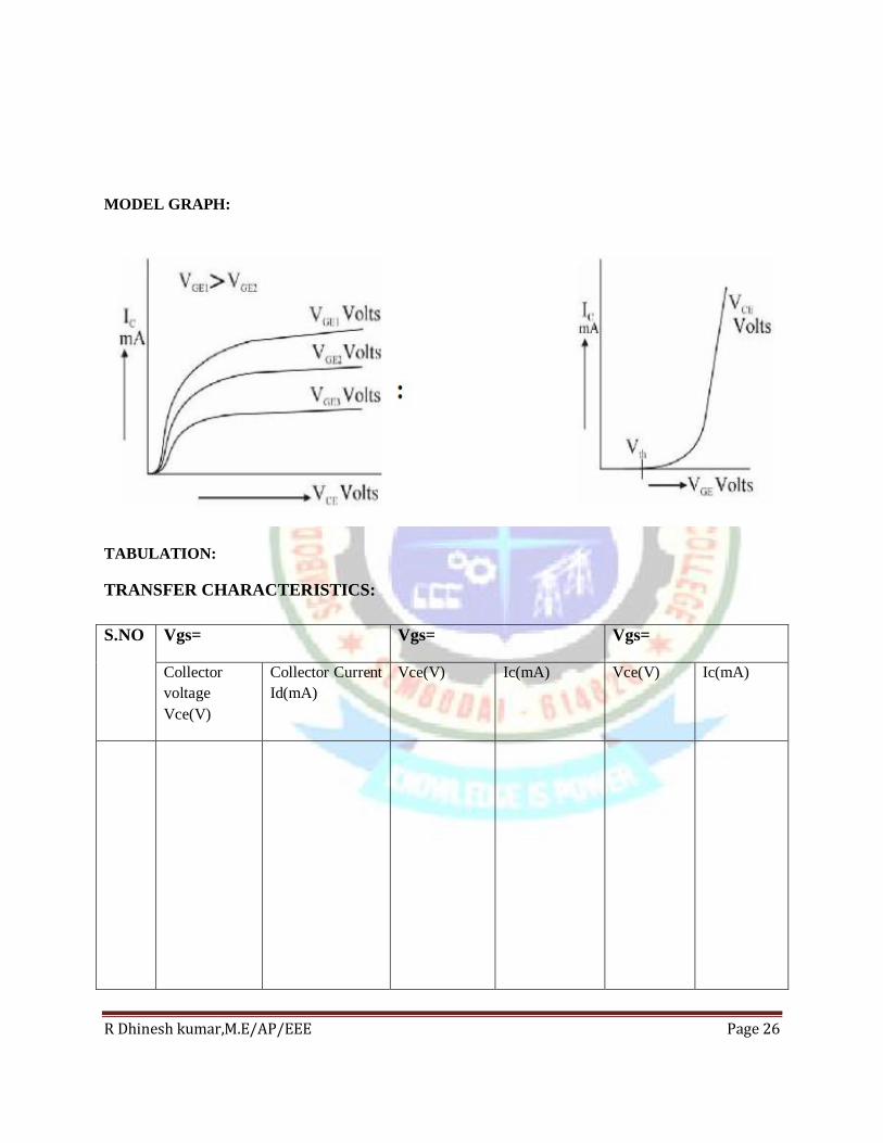
MODEL GRAPH:
TABULATION:
TRANSFER CHARACTERISTICS:
S.NO Vgs= Vgs= Vgs=
Collector
voltage
Vce(V)
Collector Current
Id(mA)
Vce(V) Ic(mA) Vce(V) Ic(mA)

R Dhinesh kumar,M.E/AP/EEE Page 27
COLLECTOR CHARACTERISTICS:
Collector Voltage Vce=
S.NO Gate Voltage Vgs(V) Collector Current Id(mA)
VIVA QUESTIONS: -
1. Why IGBT is very popular nowadays?
2. IGBT is a voltage controlled device. Why?
3. MOSFET is a voltage controlled device. Why?
4. List the different types of power MOFET.
5. State the applications of MOSFET
RESULT:
Thus the output characteristics and transfer characteristics of IGBT was obtained.

R Dhinesh kumar,M.E/AP/EEE Page 28
EX.NO:
AC TO DC HALF CONTROLLED CONVERTER DATE :
AIM:
To construct a single phase half controlled Converter and plot its output response.
APPARATUS REQUIRED:
S.NO. APPARATUS RANGE TYPE QUANTITY
1 Half controlled Converter
Power circuit kit 1, 230V,10A - 1
3 SCR firing circuit kit 1 ,230V,5A - 1
4 Isolation Transformer 230V/115-55-0-
55-115 - 1
5 Auto-transformer 230V/0-270V, 4A - 1
6 Loading Rheostat 100 / 2A - 1
7 CRO 20MHz - 1
8 Patch chords - - 15
FORMULA:
t
Firing angle α0 = --------- x 180
10ms
t= non-conducting period of thyristor.
PROCEDURE:
1. Make the connections as per the circuit diagram.
2. Keep the multiplication factor of the CRO’s probe at the maximum position.
3. Switch on the thyristor kit and firing circuit kit.
4. Keep the firing circuit knob at the 180 position. 5. Vary the firing angle in steps.
6. Note down the voltmeter reading and waveform from the CRO.
7. Switch off the power supply and disconnect.
R Dhinesh kumar,M.E/AP/EEE Page 29
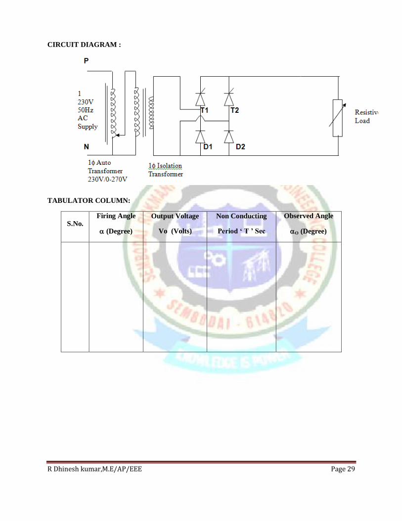
CIRCUIT DIAGRAM :
TABULATOR COLUMN:
S.No. Firing Angle
(Degree)
Output Voltage
Vo (Volts)
Non Conducting
Period ‘ T ’ Sec
Observed Angle
O (Degree)

R Dhinesh kumar,M.E/AP/EEE Page 30
MODEL GRAPH:
VIVA QUESTIONS: -
1. Define firing angle of phase controlled rectifiers.
2. What is meant by half controlled converter?
3. What are the devices can be used as a switch for half controlled rectifier?
4. Mention the nature of load current in R and RL load.
5. Mention some of the applications of controlled rectifier.
RESULT :
Thus a single-phase half controlled converter was constructed and their Output waveforms were
plotted.

R Dhinesh kumar,M.E/AP/EEE Page 31
EX.NO:
AC TO DC FULL CONTROLLED CONVERTER DATE :
AIM:
To construct a single phase fully controlled Converter and plot its response.
APPARATUS REQUIRED:
S.NO ITEM RANGE TYPE QUANTITY
1 Fully controlled
Converter Power
circuit kit
1, 230V,10A - 1
3 SCR firing circuit kit 1 ,230V,5A - 1
4 Isolation Transformer 230V/115-55-0-55-115 - 1
5 Auto-transformer 230V/0-270V, 4A - 1
6 Loading Rheostat 100 / 2A - 1
7 CRO 20MHz - 1
8 Patch chords - - 15
FORMULA :
Firing angle α0 = --------- x 180
10ms
t= non-conducting period of thyristor.
PROCEDURE:
1. Make the connections as per the circuit diagram..
2. Keep the multiplication factor of the CRO’s probe at the maximum position.
3. Switch on the thyristor kit and firing circuit kit.
4. Keep the firing circuit knob at the 180 position. 5. Vary the firing angle in steps. 6. Note down the voltmeter reading and waveform from the CRO.
7. Switch off the power supply and disconnect.

R Dhinesh kumar,M.E/AP/EEE Page 32
CIRCUIT DIAGRAM :
TABULAR COLUMN:
S.No. Firing angle
(degree)
Output voltage
Vo (volts)
Non conducting
Period ‘ t ’ sec
Observed angle
o (degree)

R Dhinesh kumar,M.E/AP/EEE Page 33
MODEL GRAPH :
VIVA QUESTIONS: -
1. What is the difference between fully controlled and half controlled converters?
2. What is meant by conduction angle?
3. What is meant by fully controlled converter?
4. Explain the nature of load current in continuous and discontinuous mode of operation.
5. What is commutation angle or overlap angle?
RESULT:
Thus a single-phase fully controlled converter was constructed and their responses were plotted.
R Dhinesh kumar,M.E/AP/EEE Page 34
EX.NO:
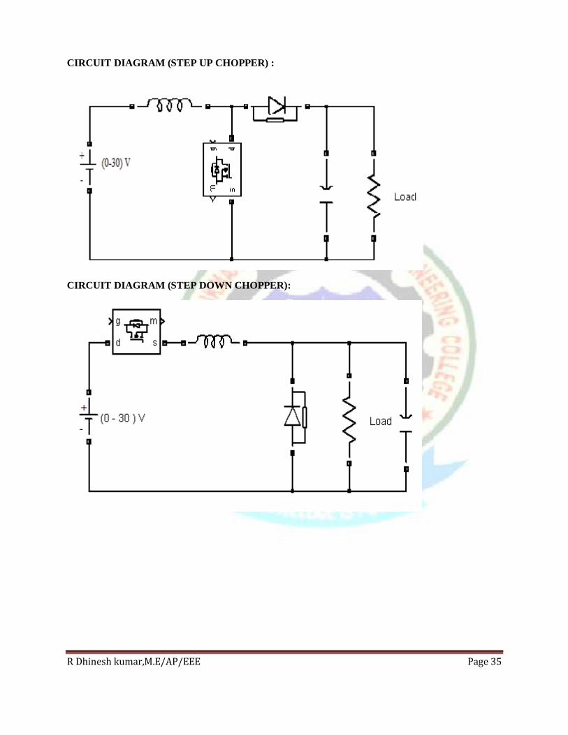
STEP UP AND STEP DOWN MOSFET BASED CHOPPERS DATE :
AIM:
To construct Step down & Step up MOSFET based choppers and to draw its output response.
APPARATUS REQUIRED:
S.NO ITEM RANGE QUANTITY
1 Step up & Step down MOSFET
based chopper kit
1
2 CRO 20 MHZ 1
3 Patch chords 15
THEORY:
This experiment is intended to study the closed loop operation of buck boost converter. The set
voltage to the PWM generator is set at 1 V. Feedback voltage from Buck Boost converter power circuit is connected to the PWM generator circuit . On varying the DC input voltage slowly from 0 to 15 v, the
output voltage is measured as constant. These values are tabulated.
PROCEDURE (STEP UP CHOPPER & STEP DOWN CHOPPER) :
1. Initially keep all the switches in the OFF position
2. Initially keep duty cycle POT in minimum position
3. Connect banana connector 24V DC source to 24V DC imput.
4. Connect the driver pulse [output to MOSFET input
5. Switch on the main supply
6. Check the test point waveforms with respect to ground.
7. Vary the duty cyle POT and tabulate the Ton, Toff & output voltage
8. Trace the waveforms of Vo Vs & Io
9. Draw the graph for Vo Vs Duty cycle, K
R Dhinesh kumar,M.E/AP/EEE Page 35
CIRCUIT DIAGRAM (STEP UP CHOPPER) :
CIRCUIT DIAGRAM (STEP DOWN CHOPPER):
R Dhinesh kumar,M.E/AP/EEE Page 36
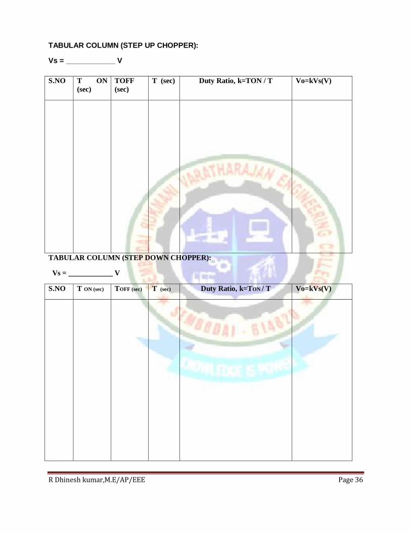
TABULAR COLUMN (STEP UP CHOPPER):
Vs = ____________ V
S.NO T ON
(sec)
TOFF
(sec)
T (sec) Duty Ratio, k=TON / T Vo=kVs(V)
TABULAR COLUMN (STEP DOWN CHOPPER):
Vs = ____________ V
S.NO T ON (sec) TOFF (sec) T (sec) Duty Ratio, k=TON / T Vo=kVs(V)

R Dhinesh kumar,M.E/AP/EEE Page 37
MODEL GRAPH (STEP UP CHOPPER) :
MODEL GRAPH (STEP DOWN CHOPPER) :
VIVA QUESTIONS: -
1. Define Buck converter.
2. Define Boost converter.
3. Enlist the control methods of DC-DC converter.
4. What are the advantages of DC-DC converter?
5. What are the applications of DC-DC converter?

R Dhinesh kumar,M.E/AP/EEE Page 38
RESULT:
Thus the output response of Step down & Step up MOSFET based choppers were drawn.

R Dhinesh kumar,M.E/AP/EEE Page 39
EX.NO:
IGBT BASED SINGLE PHASE PWM INVERTER DATE :
AIM :
To obtain Single phase output wave forms for IGBT based PWM inverter.
APPARATUS REQUIRED:
S.No. ITEM RANGE TYPE QUANTITY
1 IGBT Based PWM inverter Kit 220/10A 1
2 CRO 20MHZ 1
3 Patch Chord 10
4 Load rheostat 50/5A 1
THEORY:
It consist of four IGBTs S1,S2,S3,S4 and four inverse parallel diodes D1,D2,D3,D4 . The diodes
are essential to conduct the reactive current, and thereby to feed back the stored energy in the inductor to
the DC source. These diodes are known as feed back diodes. For many industrial applications the output AC voltage of the inverter must be sinusoidal in shape and the amplitude and freguency must be
controllable. This is achieved by PWM of the inverter switches.
The switching sequence of the inverter switches in this case, is obtained by comparing a sinusoidal control signal, of adjustable amplitude and frequency with a fixed frequency triangular carrier.
The frequency of the triangular carrier wave determines the switching frequency of the inverter switches.
The frequency of the sinusoidal control signal decides the fundamental frequency of the inverter output voltage, and is also called the modulating frequency. The sinusoidal pulse width modulation can be
programmed to have either bipolar voltage switching or unipolar voltage switching. The unipolar
switching has the advantages of effectively doubling the switching frequency as compared to the bipolar voltage switching.
PROCEDURE :
1. Make the connection as per the circuit diagram.
2. Connect the gating signal from the inverter module.
3. Switch ON D.C 24 V. 4. Keep the frequency knob to particulars frequency.
5. Observe the rectangular and triangular carrier waveforms on the CRO.
6. Obtain the output waveform across the load Rheostat

R Dhinesh kumar,M.E/AP/EEE Page 40
CIRCUIT DIAGRAM:
TABULAR COLUMN:
S.no Output voltage (v) Time (ms)
D2
D3 D1
-
+
24V,D.C
Vo
D4
T1
T2
T3
T4
50/5A
C1
C2

R Dhinesh kumar,M.E/AP/EEE Page 41
MODEL GRAPH:
VIVA QUESTIONS: -
1. What is meant by PWM control?
2. What are the advantages and disadvantages of PWM technique?
3. Name the different types of PWM techniques?
4. What is an inverter?
5. What are the applications of inverter?
RESULT :
Thus the output waveform for IGBT inverter (PWM) was obtained
t
t
Vref
Vcar
Vo
R Dhinesh kumar,M.E/AP/EEE Page 42
EX.NO:
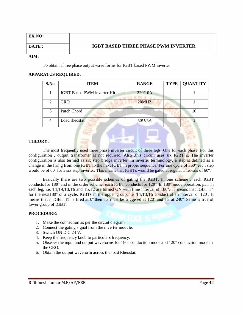
IGBT BASED THREE PHASE PWM INVERTER DATE :
AIM:
To obtain Three phase output wave forms for IGBT based PWM inverter
APPARATUS REQUIRED:
S.No. ITEM RANGE TYPE QUANTITY
1 IGBT Based PWM inverter Kit 220/10A 1
2 CRO 20MHZ 1
3 Patch Chord 10
4 Load rheostat 50/5A 1
THEORY:
The most frequently used three phase inverter circuit of three legs, One for each phase. For this configuration , output transformer is not required. Also ,this circuit uses six IGBT s. The inverter
configuration is also termed as six step bridge inverter. In inverter terminology, a step is defined as a
change in the firing from one IGBT to the next IGBT in proper sequence. For one cycle of 360º,each step
would be of 60º for a six step inverter. This means that IGBTs would be gated at regular intervals of 60º.
Basically there are two possible schemes of gating the IGBT. In one scheme , each IGBT
conducts for 180º and in the order scheme, each IGBT conducts for 120º. In 180º mode operation, pair in each leg, i.e. T1,T4,T3,T6 and T5,T2 are turned ON with time interval of 180º. IT means that IGBT T4
for the next180º of a cycle. IGBTs in the upper group, i.e. T1,T3,T5 conduct at an interval of 120º. It
means that if IGBT T1 is fired at 0º,then T3 must be triggered at 120º and T5 at 240º. Same is true of lower group of IGBT.
PROCEDURE:
1. Make the connection as per the circuit diagram.
2. Connect the gating signal from the inverter module.
3. Switch ON D.C 24 V. 4. Keep the frequency knob to particulars frequency.
5. Observe the input and output waveforms for 180° conduction mode and 120° conduction mode in
the CRO. 6. Obtain the output waveform across the load Rheostat.

R Dhinesh kumar,M.E/AP/EEE Page 43
CIRCUIT DIAGRAM:
TABULAR COLUMN:
S.No. Output Voltage (V) Time (ms)

R Dhinesh kumar,M.E/AP/EEE Page 44
MODEL GRAPH :
VIVA QUESTIONS: -
1. What are the main classifications of inverters?
2. Why thyristors are not preferred for inverters?
3. What is main drawbacks of a half bridge inverters?
4. Give two advantages of CSI.
5. Why diodes should be connected in anti parallel with IGBT in inverter?
RESULT :
Thus the output waveform for IGBT inverter (PWM) was obtained.

R Dhinesh kumar,M.E/AP/EEE Page 45
EX.NO: AC VOLTAGE CONTROLLER
DATE :
AIM:
To construct a single phase full wave AC voltage controller and plot its output response.
APPARATUS REQUIRED:
S.No. ITEM RANGE TYPE QUANTITY
1 Single phase AC voltage controller
Kit
220/10A 1
2 CRO 20MHZ 1
3 Patch Chord 10
4 Load rheostat 50/5A 1
PROCEDURE:
1. Make the connection as per the circuit diagram.
2. Connect the gating signal from the module.
3. Switch ON A.C supply.
4. Set the firing angle.
5. Obtain the output waveform across the load Rheostat.

R Dhinesh kumar,M.E/AP/EEE Page 46
CIRCUIT DIAGRAM
MODEL GRAPH:

R Dhinesh kumar,M.E/AP/EEE Page 47
TABULAR COLUMN:
S.No. Firing angle (α) Output Voltage (V) Time (ms)

R Dhinesh kumar,M.E/AP/EEE Page 48
VIVA QUESTIONS: -
1. What is meant by AC voltage controller?
2. What are the applications of AC voltage controller?
3. What are the advantages and disadvantages of AC voltage controller?
4. What are the two methods of control in AC voltage controller?
5. What is the difference between AC voltage controller and Cyclo Converter?
RESULT :

R Dhinesh kumar,M.E/AP/EEE Page 49
EX.NO:
SWITCHED MODE POWER CONVERTER DATE :
AIM:
To construct a switched mode power converters and plot its output response.
APPARATUS REQUIRED:
S.No. ITEM RANGE TYPE QUANTITY
1 Switched mode power converter Kit 220/10A 1
2 CRO 20MHZ 1
3 Patch Chord 10
4 Load rheostat 50/5A 1
PROCEDURE:
1. Make the connection as per the circuit diagram.
2. Connect the gating signal from the module.
3. Switch ON D.C supply.
4. Obtain the output waveform across the load Rheostat.
CIRCUIT DIAGRAM (BUCK CONVERTER):
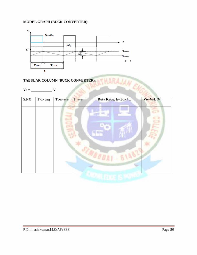
R Dhinesh kumar,M.E/AP/EEE Page 50
MODEL GRAPH (BUCK CONVERTER):
TABULAR COLUMN (BUCK CONVERTER):
Vs = ____________ V
S.NO T ON (sec) TOFF (sec) T (sec) Duty Ratio, k=TON / T Vo=Vsk (V)
R Dhinesh kumar,M.E/AP/EEE Page 51
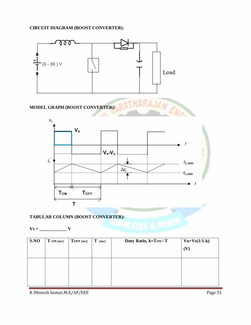
CIRCUIT DIAGRAM (BOOST CONVERTER):
MODEL GRAPH (BOOST CONVERTER):
TABULAR COLUMN (BOOST CONVERTER):
Vs = ____________ V
S.NO T ON (sec) TOFF (sec) T (sec) Duty Ratio, k=TON / T Vo=Vs(1/1-k)
(V)

R Dhinesh kumar,M.E/AP/EEE Page 52
CIRCUIT DIAGRAM (BUCK BOOST CONVERTER):
MODEL GRAPH (BUCK BOOST CONVERTER):

R Dhinesh kumar,M.E/AP/EEE Page 53
TABULAR COLUMN (BUCK BOOST CONVERTER):
Vs = ____________ V
S.NO T ON (sec) TOFF (sec) T (sec) Duty Ratio, k=TON / T Vo=-(Vsk/1-k)
(V)
VIVA QUESTIONS: -
1. What is meant by switched mode regulator?
2. What are the basic topologies of switching regulators?
3. What are the advantages and disadvantages of buck converter?
4. What are the applications of Boost converter?
5. What is meant by buck boost converter?
RESULT :
R Dhinesh kumar,M.E/AP/EEE Page 54
EX.NO:
SIMULATION OF SINGLE PHASE SEMI CONVERTER DATE :
AIM:
To analyze the characteristics of single phase semi converter with R and RL load using MATLAB and
Simulink.
APPARATUS REQUIRED:
S.No. SOFTWARE TYPE QUANTITY
1 MATLAB SIMULATION 1
PROCEDURE:
1. Open the MATLAB software.
2. Create a new model.
3. Go to simulink library and take the necessary components as per the circuit diagram.
4. Draw the Matlab circuit and simulate with the help of scope.
5. Verify and analyze the output waveforms.

R Dhinesh kumar,M.E/AP/EEE Page 55
MATLAB CIRCUIT DIAGRAM (R- LOAD)
OUTPUT:
R Dhinesh kumar,M.E/AP/EEE Page 56
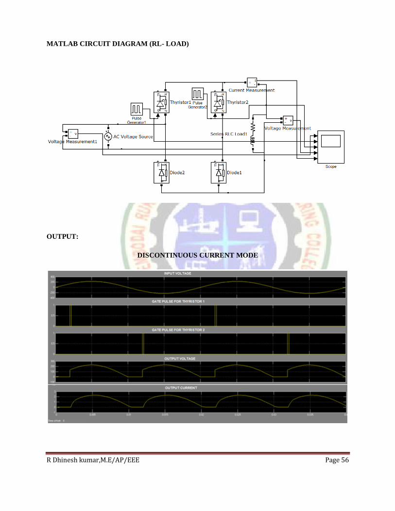
MATLAB CIRCUIT DIAGRAM (RL- LOAD)
OUTPUT:
DISCONTINUOUS CURRENT MODE

R Dhinesh kumar,M.E/AP/EEE Page 57
OUTPUT:
CONTINUOUS CURRENT MODE
PARAMETERS TO BE ENTERED:
(R- LOAD):
AC VOLTAGE SOURCE
Peak amplitude : 230V
Frequency : 50Hz
PULSE GENERATOR 1
Amplitude : 1
Period : 0.02 sec
Pulse width : 1
Phase Delay : 0.002 sec
R Dhinesh kumar,M.E/AP/EEE Page 58
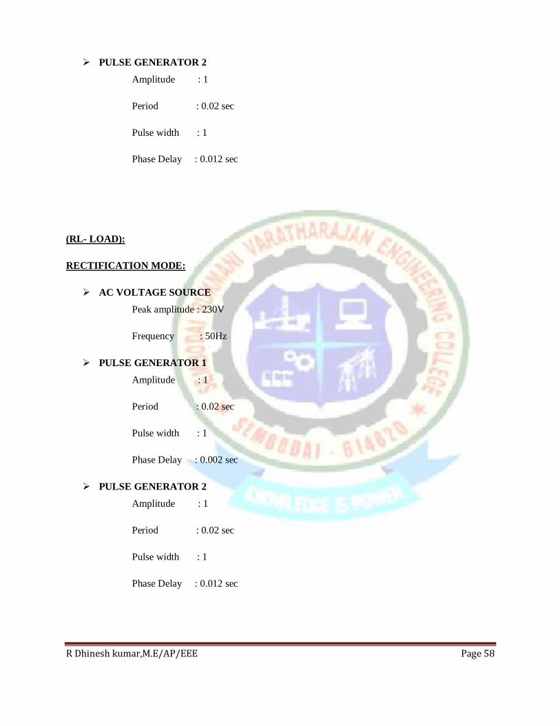
PULSE GENERATOR 2
Amplitude : 1
Period : 0.02 sec
Pulse width : 1
Phase Delay : 0.012 sec
(RL- LOAD):
RECTIFICATION MODE:
AC VOLTAGE SOURCE
Peak amplitude : 230V
Frequency : 50Hz
PULSE GENERATOR 1
Amplitude : 1
Period : 0.02 sec
Pulse width : 1
Phase Delay : 0.002 sec
PULSE GENERATOR 2
Amplitude : 1
Period : 0.02 sec
Pulse width : 1
Phase Delay : 0.012 sec
R Dhinesh kumar,M.E/AP/EEE Page 59
RL LOAD
(FOR CONTINUOUS CURRENT):
Inductive reactive power QL: 9000 (positive VAR)
(FOR DISCONTINUOUS CURRENT):
Inductive reactive power QL: 1000 (positive VAR)
RESULT :

R Dhinesh kumar,M.E/AP/EEE Page 60
EX.NO:
SIMULATION OF SINGLE PHASE FULL CONVERTER DATE :
AIM:
To analyze the characteristics of single phase full converter with R, RL and RLE load with rectification
and inversion mode for continuous and discontinuous currents using MATLAB and Simulink.
APPARATUS REQUIRED:
S.No. SOFTWARE TYPE QUANTITY
1 MATLAB SIMULATION 1
PROCEDURE:
1. Open the MATLAB software.
1. Create a new model.
2. Go to simulink library and take the necessary components as per the circuit diagram.
3. Draw the Matlab circuit and simulate with the help of scope.
4. Verify and analyze the output waveforms.

R Dhinesh kumar,M.E/AP/EEE Page 61
MATLAB CIRCUIT DIAGRAM (R- LOAD)
OUTPUT:

R Dhinesh kumar,M.E/AP/EEE Page 62
MATLAB CIRCUIT DIAGRAM (RL- LOAD)
OUTPUT:
DISCONTINUOUS CURRENT MODE (RECTIFICATION MODE)
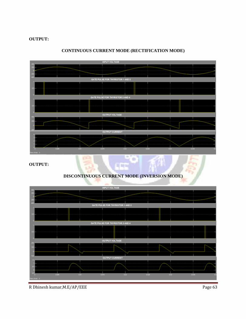
R Dhinesh kumar,M.E/AP/EEE Page 63
OUTPUT:
CONTINUOUS CURRENT MODE (RECTIFICATION MODE)
OUTPUT:
DISCONTINUOUS CURRENT MODE (INVERSION MODE)

R Dhinesh kumar,M.E/AP/EEE Page 64
MATLAB CIRCUIT DIAGRAM (RLE- LOAD)
OUTPUT:
DISCONTINUOUS CURRENT MODE (RECTIFICATION MODE)

R Dhinesh kumar,M.E/AP/EEE Page 65
PARAMETERS TO BE ENTERED:
(R- LOAD):
AC VOLTAGE SOURCE
Peak amplitude : 230V
Frequency : 50Hz
PULSE GENERATOR 1 ( FOR THYRISTOR 1 AND 2)
Amplitude : 1
Period : 0.02 sec
Pulse width : 1
Phase Delay : 0.002 sec
PULSE GENERATOR 2 ( FOR THYRISTOR 3 AND 4)
Amplitude : 1
Period : 0.02 sec
Pulse width : 1
Phase Delay : 0.012 sec
(RL- LOAD):
RECTIFICATION MODE:
AC VOLTAGE SOURCE
Peak amplitude : 230V
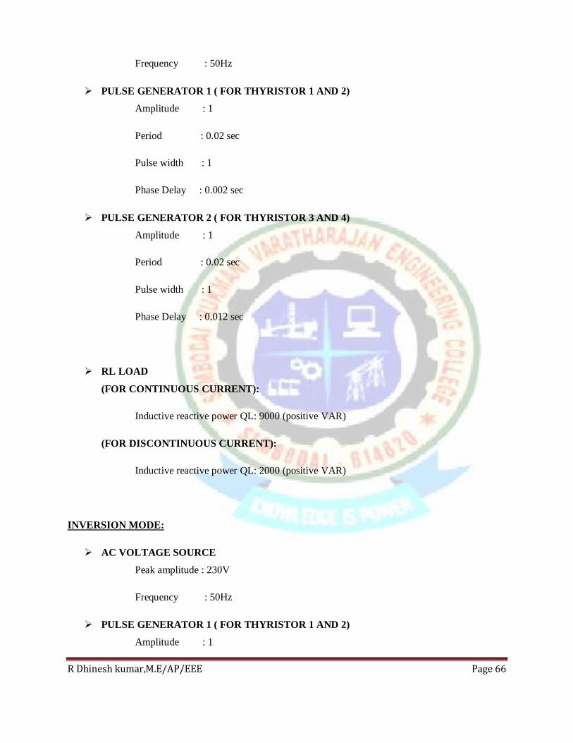
R Dhinesh kumar,M.E/AP/EEE Page 66
Frequency : 50Hz
PULSE GENERATOR 1 ( FOR THYRISTOR 1 AND 2)
Amplitude : 1
Period : 0.02 sec
Pulse width : 1
Phase Delay : 0.002 sec
PULSE GENERATOR 2 ( FOR THYRISTOR 3 AND 4)
Amplitude : 1
Period : 0.02 sec
Pulse width : 1
Phase Delay : 0.012 sec
RL LOAD
(FOR CONTINUOUS CURRENT):
Inductive reactive power QL: 9000 (positive VAR)
(FOR DISCONTINUOUS CURRENT):
Inductive reactive power QL: 2000 (positive VAR)
INVERSION MODE:
AC VOLTAGE SOURCE
Peak amplitude : 230V
Frequency : 50Hz
PULSE GENERATOR 1 ( FOR THYRISTOR 1 AND 2)
Amplitude : 1
R Dhinesh kumar,M.E/AP/EEE Page 67
Period : 0.02 sec
Pulse width : 1
Phase Delay : 0.0075 sec
PULSE GENERATOR 2 ( FOR THYRISTOR 3 AND 4)
Amplitude : 1
Period : 0.02 sec
Pulse width : 1
Phase Delay : 0.0175sec
RL LOAD
(FOR DISCONTINUOUS CURRENT):
Inductive reactive power QL: 2000 (positive VAR)
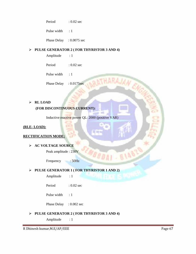
(RLE- LOAD):
RECTIFICATION MODE:
AC VOLTAGE SOURCE
Peak amplitude : 230V
Frequency : 50Hz
PULSE GENERATOR 1 ( FOR THYRISTOR 1 AND 2)
Amplitude : 1
Period : 0.02 sec
Pulse width : 1
Phase Delay : 0.002 sec
PULSE GENERATOR 2 ( FOR THYRISTOR 3 AND 4)
Amplitude : 1
R Dhinesh kumar,M.E/AP/EEE Page 68
Period : 0.02 sec
Pulse width : 1
Phase Delay : 0.012 sec
RL LOAD
(FOR DISCONTINUOUS CURRENT):
Inductive reactive power QL: 4000 (positive VAR)
DC VOLTAGE SOURCE (E):
Amplitude : 50 V.
RESULT :

R Dhinesh kumar,M.E/AP/EEE Page 69
EX.NO:
SIMULATION OF DC-DC STEP DOWN CONVERTER DATE :
AIM:
To analyze the characteristics of DC-DC step down converter with R, RL and RLE load using MATLAB
and Simulink.
APPARATUS REQUIRED:
S.No. SOFTWARE TYPE QUANTITY
1 MATLAB SIMULATION 1
PROCEDURE:
1. Open the MATLAB software.
2. Create a new model.
3. Go to simulink library and take the necessary components as per the circuit diagram.
4. Draw the Matlab circuit and simulate with the help of scope.
5. Verify and analyze the output waveforms.

R Dhinesh kumar,M.E/AP/EEE Page 70
MATLAB CIRCUIT DIAGRAM (R- LOAD)
OUTPUT:
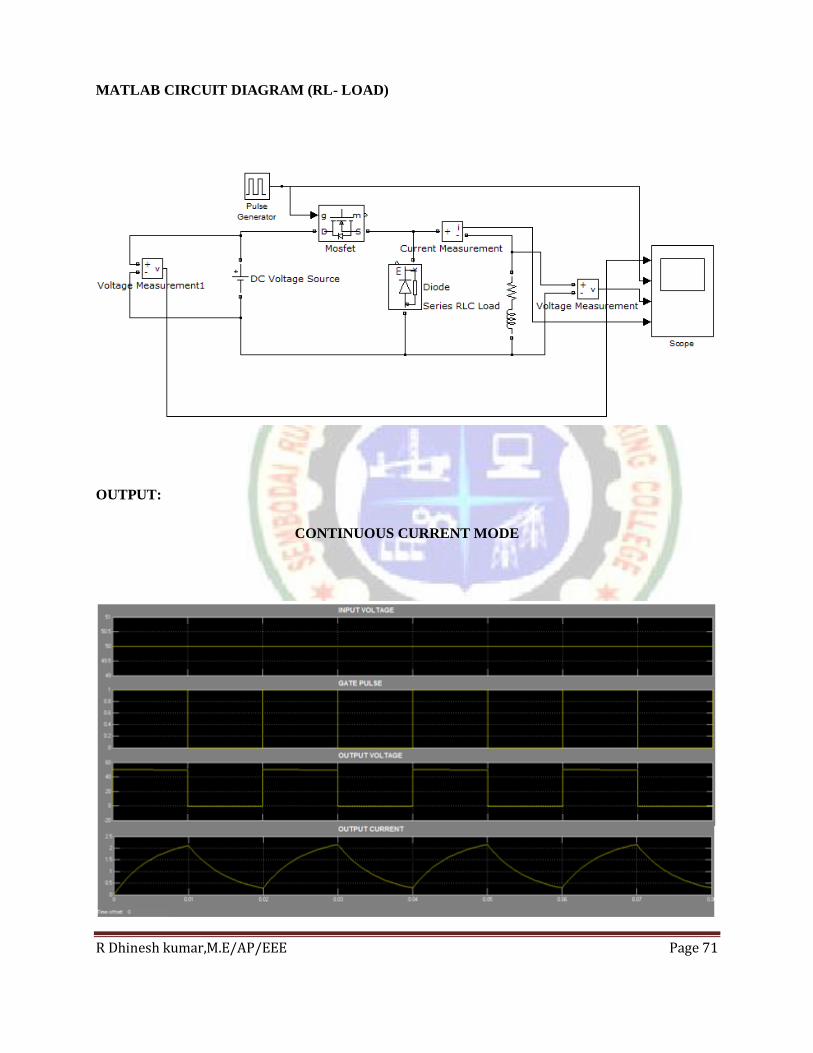
R Dhinesh kumar,M.E/AP/EEE Page 71
MATLAB CIRCUIT DIAGRAM (RL- LOAD)
OUTPUT:
CONTINUOUS CURRENT MODE
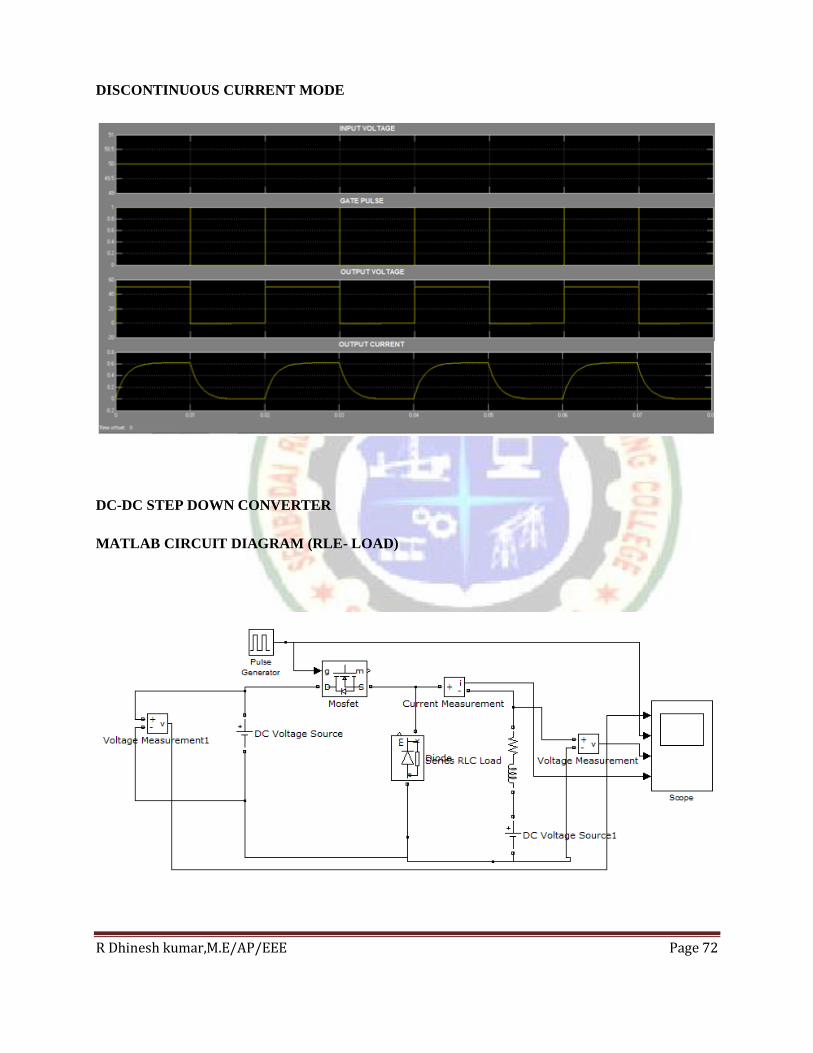
R Dhinesh kumar,M.E/AP/EEE Page 72
DISCONTINUOUS CURRENT MODE
DC-DC STEP DOWN CONVERTER
MATLAB CIRCUIT DIAGRAM (RLE- LOAD)

R Dhinesh kumar,M.E/AP/EEE Page 73
OUTPUT:
CONTINUOUS CURRENT MODE
DISCONTINUOUS CURRENT MODE

R Dhinesh kumar,M.E/AP/EEE Page 74
PARAMETERS TO BE ENTERED:
(R- LOAD):
DC VOLTAGE SOURCE
Amplitude : 50V
PULSE GENERATOR
Amplitude : 1
Period : 0.02 sec
Pulse width : 50
Phase Delay : 0 sec
(RL- LOAD):
DC VOLTAGE SOURCE
Amplitude : 50V
PULSE GENERATOR 1
Amplitude : 1
Period : 0.02 sec
Pulse width : 50
Phase Delay : 0 sec
RL LOAD
(FOR CONTINUOUS CURRENT):
Inductive reactive power QL: 20000 (positive VAR)
(FOR DISCONTINUOUS CURRENT):
Inductive reactive power QL: 5000 (positive VAR)
R Dhinesh kumar,M.E/AP/EEE Page 75
(RLE- LOAD):
DC VOLTAGE SOURCE
Amplitude : 50V
PULSE GENERATOR
Amplitude : 1
Period : 0.02 sec
Pulse width : 50
Phase Delay : 0 sec
RL LOAD
(FOR CONTINUOUS CURRENT):
Inductive reactive power QL: 50000 (positive VAR)
(FOR DISCONTINUOUS CURRENT):
Inductive reactive power QL: 10000 (positive VAR)
DC VOLTAGE SOURCE (E):
Amplitude : 10 V.
RESULT :

R Dhinesh kumar,M.E/AP/EEE Page 76
EX.NO:
SIMULATION OF SINGLE PHASE AC VOLTAGE
CONTROLLER
DATE :
AIM:
To analyze the characteristics of single phase full wave AC voltage controller with R and RL load using
MATLAB and Simulink.
APPARATUS REQUIRED:
S.No. SOFTWARE TYPE QUANTITY
1 MATLAB SIMULATION 1
PROCEDURE:
1. Open the MATLAB software.
2. Create a new model.
3. Go to simulink library and take the necessary components as per the circuit diagram.
4. Draw the Matlab circuit and simulate with the help of scope.
5. Verify and analyze the output waveforms.

R Dhinesh kumar,M.E/AP/EEE Page 77
MATLAB CIRCUIT DIAGRAM (R- LOAD)
OUTPUT

R Dhinesh kumar,M.E/AP/EEE Page 78
MATLAB CIRCUIT DIAGRAM (RL- LOAD)
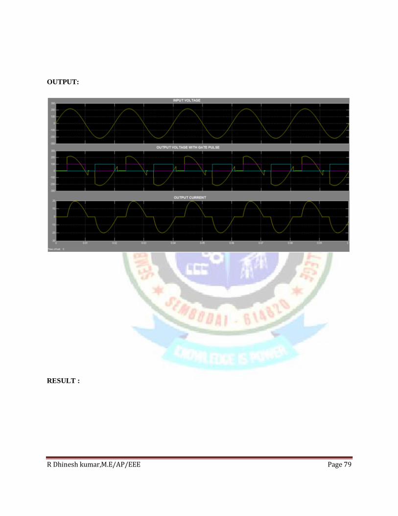
R Dhinesh kumar,M.E/AP/EEE Page 79
OUTPUT:
RESULT :