sembodai rukmani varatharajan engineering college …€¦ · 4. single tuned amplifier 5. rc...
TRANSCRIPT
SRV ENGINEERING COLLEGE B.E (ELECTRONICS & COMMUNICATION ENGINEERING)
EC6411-CIRCUITS & SIMULATION INTEGRATED LAB R.SHANKARANARAYANAN,AP/ECE/SRVEC
SEMBODAI RUKMANI VARATHARAJAN ENGINEERING
COLLEGE
SEMBODAI – 614809 (Approved By AICTE,Newdelhi – Affiliated To ANNA UNIVERSITY::Chennai)
EC6411
CIRCUITS AND SIMULATION INTEGRATED
LABORATORY (REGULATION-2013)
LAB MANUAL
DEPARTMENT OF ELECTRONICS &
COMMUNICATION ENGINEERING
Prepared By, Approved By, R.SHANKARANARAYANAN, G.SUNDAR
AP/ECE/SRVEC HOD/ECE/SRVEC

SRV ENGINEERING COLLEGE B.E (ELECTRONICS & COMMUNICATION ENGINEERING)
2 EC6411-CIRCUITS & SIMULATION INTEGRATED LAB R.SHANKARANARAYANAN,AP/ECE/SRVEC
(REGULATION 2013) AS PER ANNA UNIVERSITY SYLLABUS
SYLLABUS
LIST OF EXPERIMENTS:
DESIGN AND ANALYSIS OF;
1. Series and Shunt feedback amplifiers-Frequency response, Input and output
impedance calculation
2. RC Phase shift oscillator and Wien Bridge Oscillator
3. Hartley Oscillator and Colpitts Oscillator
4. Single Tuned Amplifier
5. RC Integrator and Differentiator circuits
6. Astable and Monostable multivibrators
7. Clippers and Clampers
8. Free running Blocking Oscillators
SIMULATION USING SPICE:
1. Tuned Collector Oscillator
2. Twin -T Oscillator / Wein Bridge Oscillator
3. Double and Stagger tuned Amplifiers
4. Bistable Multivibrator
5. Schmitt Trigger circuit with Predictable hysteresis
6. Monostable multivibrator with emitter timing and base timing
7. Voltage and Current Time base circuits

SRV ENGINEERING COLLEGE B.E (ELECTRONICS & COMMUNICATION ENGINEERING)
EC6411-CIRCUITS & SIMULATION INTEGRATED LAB R.SHANKARANARAYANAN,AP/ECE/SRVEC
CONTENTS
Exp.
No DATE TITLE OF EXPERIMENTS PAGE MARK SIGNATURE
CYCLE - I
1
Series and Shunt feedback amplifiers-
Frequency response, Input and output
impedance Calculation
2
Wien Bridge Oscillator
RC Phase shift oscillator
3 Hartley Oscillator and Colpitts Oscillator
4 Single Tuned Amplifier
5 RC Integrator and Differentiator circuits
6 Astable and Monostable multivibrators
7 Clippers and Clampers
8 Free running Blocking Oscillators
CYCLE – II
1 Tuned Collector Oscillator
2 Twin -T Oscillator / Wein Bridge Oscillator
3 Double and Stagger tuned Amplifiers
4 Bistable Multivibrator
5 Schmitt Trigger circuit with Predictable
hysteresis
6 Monostable multivibrator with emitter timing
and base timing
7 Voltage and Current Time base circuits
SRV ENGINEERING COLLEGE B.E (ELECTRONICS & COMMUNICATION ENGINEERING)
4 EC6411-CIRCUITS & SIMULATION INTEGRATED LAB R.SHANKARANARAYANAN,AP/ECE/SRVEC
EX.NO : FEED BACK AMPLIFIERS
DATE :
AIM:
To design and test the current series and voltage shunt Feedback Amplifier and to
calculate the following parameters with and without feedback.
1. Mid band gain.
2. Bandwidth and cutoff frequencies.
3. Input and output impedance.
APPARATUS REQUIRED:
S.NO ITEM RANGE Q.TY
1 TRANSISTOR BC 107 1
2 RESISTOR 1
3 CAPACITOR 4.7uf ,
47uf
2,
1
4 CRO (0-30 )MHz 1
5 RPS (0-30) V 1
6 FUNCTION
GENERATOR
(0 – 1 )MHZ 1
CIRCUIT DIAGRAM: WITHOUT FEEDBACK:
+VCC
58k 4.5k 4.7uf
BC107
4.7uf E
Vo
CE
Vin R2 12k 1k 47uf
F = 1 KHz
CRO
SRV ENGINEERING COLLEGE B.E (ELECTRONICS & COMMUNICATION ENGINEERING)
EC6411-CIRCUITS & SIMULATION INTEGRATED LAB R.SHANKARANARAYANAN,AP/ECE/SRVEC
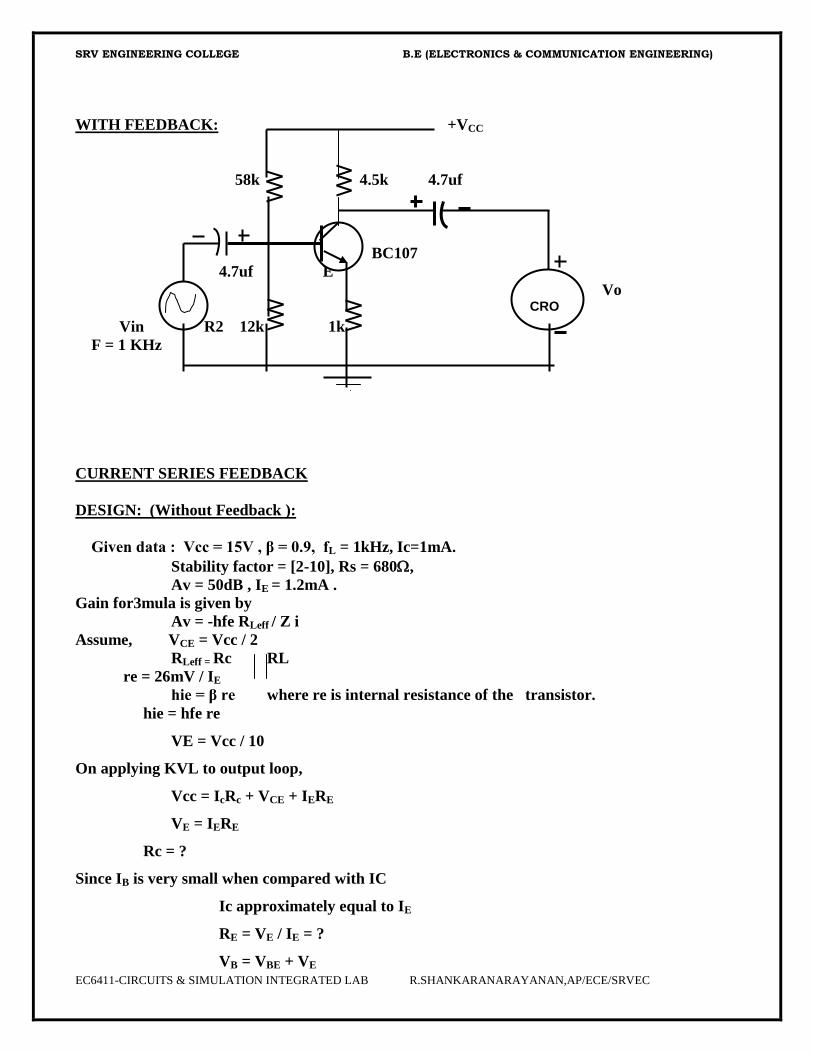
WITH FEEDBACK: +VCC
58k 4.5k 4.7uf
BC107
4.7uf E
Vo
Vin R2 12k 1k
F = 1 KHz
CURRENT SERIES FEEDBACK
DESIGN: (Without Feedback ):
Given data : Vcc = 15V , β = 0.9, fL = 1kHz, Ic=1mA.
Stability factor = [2-10], Rs = 680,
Av = 50dB , IE = 1.2mA .
Gain for3mula is given by
Av = -hfe RLeff / Z i
Assume, VCE = Vcc / 2
RLeff = Rc RL
re = 26mV / IE
hie = β re where re is internal resistance of the transistor.
hie = hfe re
VE = Vcc / 10
On applying KVL to output loop,
Vcc = IcRc + VCE + IERE
VE = IERE
Rc = ?
Since IB is very small when compared with IC
Ic approximately equal to IE
RE = VE / IE = ?
VB = VBE + VE
CRO

SRV ENGINEERING COLLEGE B.E (ELECTRONICS & COMMUNICATION ENGINEERING)
6 EC6411-CIRCUITS & SIMULATION INTEGRATED LAB R.SHANKARANARAYANAN,AP/ECE/SRVEC
VB = VCC . RB2 / RB1 + RB2
S = 1+ (RB /RE )
RB = ?
RB = RB1 RB2
Find
Input Impedance , Zi = ( RB hie )
Coupling and bypass capacitors can be thus found out.
Input coupling capacitor is given by , Xci = Z i / 10
Xci = 1/ 2fCi
Ci = ?
output coupling capacitor is given by ,
Xco=(Rc RL) / 10
Xc0 = 1/ 2fCo
Co = ?
By-pass capacitor is given by ,XCE = 1/ 2fCE
CE = ?
Design ( With feedback ) :
Remove the emitter capacitance ( CE )
β = -1 / RE
Gm = - hfe/ [(hie + RE ) RB]
D = 1+ β Gm
Gmf = Gm / D
Zif = Z iD
Zof = ZoD
Voltage shunt DESIGN: (Without Feedback ):
Given data : Vcc = 15V , fL = 1kHz, Ic=1mA.
Stability factor = [2-10], Rs = 680,
Av =40 dB .
Gain formula is given by
Av = -hfe RLeff / Z i
Assume, VCE = Vcc / 2

SRV ENGINEERING COLLEGE B.E (ELECTRONICS & COMMUNICATION ENGINEERING)
EC6411-CIRCUITS & SIMULATION INTEGRATED LAB R.SHANKARANARAYANAN,AP/ECE/SRVEC
RLeff = R c RL
re = 26mV / IE
hie = β re where re is internal resistance of the transistor.
hie = hfe re
VE = Vcc / 10
On applying KVL to output loop,
Vcc = IcRc + VCE + IERE
VE = IERE
Rc = ?
Since IB is very small when compared with Ic
Ic approximately equal to IE
RE = VE / IE = ?
VB = VBE + VE
VB = VCC . RB2 / RB1 + RB2
S = 1+ RB / RE
RB =?
RB = RB1 RB2
Find
Input Impedance, Zi = (RB hie )
Coupling and bypass capacitors can be thus found out.
Input coupling capacitor is given by , Xci = Z i / 10
Xci = 1/ 2f Ci
Ci = ?
output coupling capacitor is given by ,
X co=(Rc | | RL) / 10
Xc0 = 1/ 2f Co
Co =?
By-pass capacitor is given by, XCE = 1/ 2f CE
CE =?
Design ( With feedback ) :
Connect the feedback resistance (Rf) and feedback capacitor (Cf) as shown in the figure.
Xcf = Rf / 10
Cf = Rf / 2πf x 10
SRV ENGINEERING COLLEGE B.E (ELECTRONICS & COMMUNICATION ENGINEERING)
8 EC6411-CIRCUITS & SIMULATION INTEGRATED LAB R.SHANKARANARAYANAN,AP/ECE/SRVEC
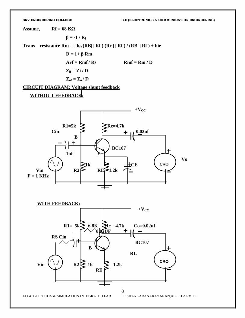
Assume, Rf = 68 K
β = -1 / Rf
Trans – resistance Rm = - hfe (RB| | Rf ) (Rc | | Rf ) / (RB| | Rf ) + hie
D = 1+ β Rm
Avf = Rmf / Rs Rmf = Rm / D
Zif = Zi / D
Zof = Zo / D
CIRCUIT DIAGRAM: Voltage shunt feedback
WITHOUT FEEDBACK:
+VCC
R1=5k Rc=4.7k
Cin 0.02uf
B
BC107
1uf E
Vo
1k CE
Vin R2 RE 1.2k
F = 1 KHz
WITH FEEDBACK:
+VCC
R1= 5k 6.8K Rc 4.7k Co=0.02uf
0.02UF
RS Cin
BC107
B
RL
Vin R R2 1k 1.2k
RE
CRO
CRO
SRV ENGINEERING COLLEGE B.E (ELECTRONICS & COMMUNICATION ENGINEERING)
EC6411-CIRCUITS & SIMULATION INTEGRATED LAB R.SHANKARANARAYANAN,AP/ECE/SRVEC
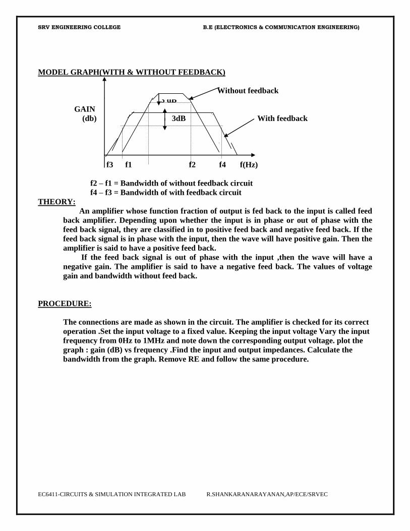
MODEL GRAPH(WITH & WITHOUT FEEDBACK)
Without feedback
3 dB
GAIN
(db) 3dB With feedback
f3 f1 f2 f4 f(Hz)
f2 – f1 = Bandwidth of without feedback circuit
f4 – f3 = Bandwidth of with feedback circuit
THEORY:
An amplifier whose function fraction of output is fed back to the input is called feed
back amplifier. Depending upon whether the input is in phase or out of phase with the
feed back signal, they are classified in to positive feed back and negative feed back. If the
feed back signal is in phase with the input, then the wave will have positive gain. Then the
amplifier is said to have a positive feed back.
If the feed back signal is out of phase with the input ,then the wave will have a
negative gain. The amplifier is said to have a negative feed back. The values of voltage
gain and bandwidth without feed back.
PROCEDURE:
The connections are made as shown in the circuit. The amplifier is checked for its correct
operation .Set the input voltage to a fixed value. Keeping the input voltage Vary the input
frequency from 0Hz to 1MHz and note down the corresponding output voltage. plot the
graph : gain (dB) vs frequency .Find the input and output impedances. Calculate the
bandwidth from the graph. Remove RE and follow the same procedure.

SRV ENGINEERING COLLEGE B.E (ELECTRONICS & COMMUNICATION ENGINEERING)
10 EC6411-CIRCUITS & SIMULATION INTEGRATED LAB R.SHANKARANARAYANAN,AP/ECE/SRVEC
OBSERVATION:
WITH OUT FEEDBACK
Vin = ------------ Volts
S.NO FREQUNCY O/P
voltage Vo Gain
Av=20 log Vo/Vi
WITH FEEDBACK
S.NO FREQUNCY O/P
voltage Av=20 log Vo/Vi
RESULT:
Theoritical Practical
With F/B Without F/B With F/B Without F/B
Input Impedance
Output
Impedance
Bandwidth
Transconductance
(gm)
SRV ENGINEERING COLLEGE B.E (ELECTRONICS & COMMUNICATION ENGINEERING)
EC6411-CIRCUITS & SIMULATION INTEGRATED LAB R.SHANKARANARAYANAN,AP/ECE/SRVEC
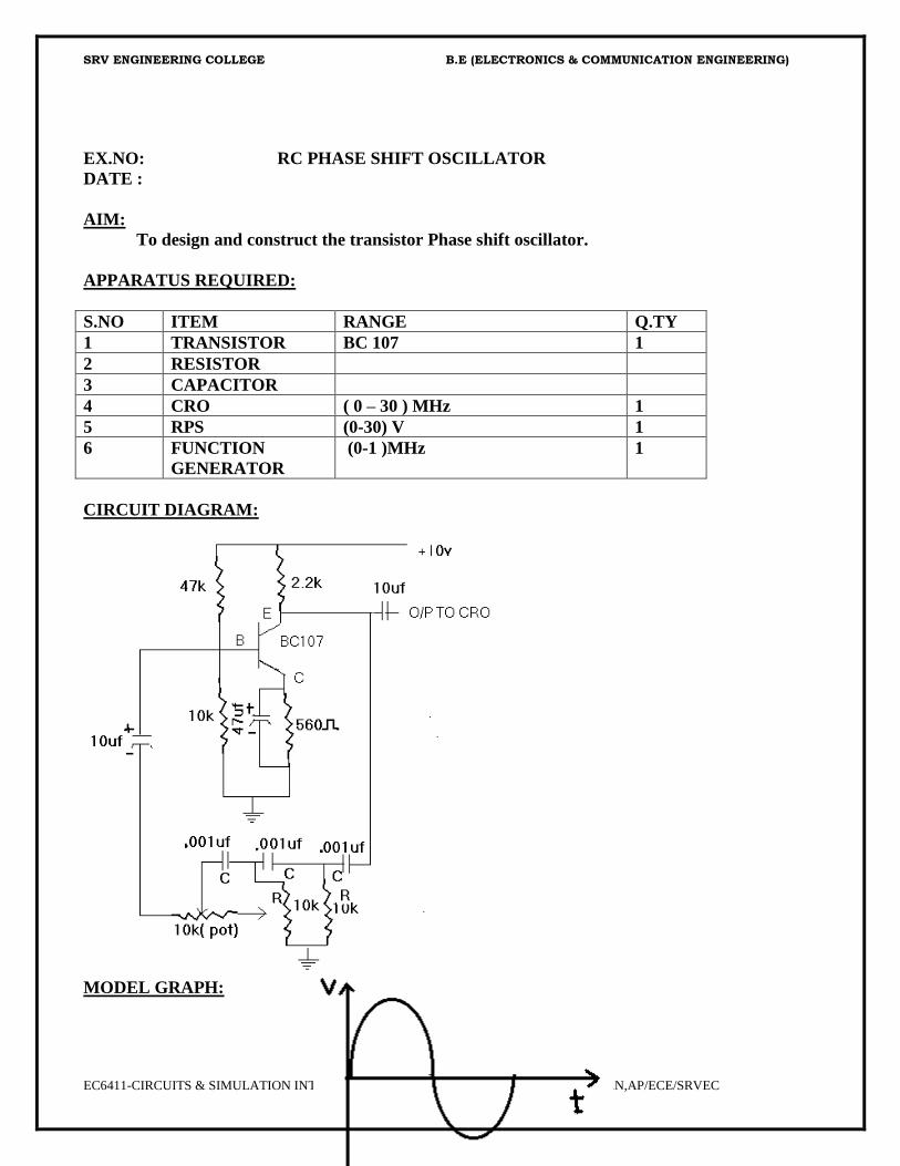
EX.NO: RC PHASE SHIFT OSCILLATOR
DATE :
AIM:
To design and construct the transistor Phase shift oscillator.
APPARATUS REQUIRED:
S.NO ITEM RANGE Q.TY
1 TRANSISTOR BC 107 1
2 RESISTOR
3 CAPACITOR
4 CRO ( 0 – 30 ) MHz 1
5 RPS (0-30) V 1
6 FUNCTION
GENERATOR
(0-1 )MHz 1
CIRCUIT DIAGRAM:
MODEL GRAPH:

SRV ENGINEERING COLLEGE B.E (ELECTRONICS & COMMUNICATION ENGINEERING)
12 EC6411-CIRCUITS & SIMULATION INTEGRATED LAB R.SHANKARANARAYANAN,AP/ECE/SRVEC
DESIGN:
Given : Vcc = 12V , fo = 1 KHz,C = 0.01µF; IE = 5mA.; Stability factor = 10
f = 1/ 2πRC Find R
R1 = (Ri – R)
R >> Rc
Βeta = -1 / 29
Amplifier Design :
Gain formula is given by
Av = -hfe RLeff / hie ( Av = 29, design given )
Assume, VCE = Vcc / 2
RLeff = R c RL
re = 26mV / IE
hie = β re where re is internal resistance of the transistor.
hie = hfe re
VE = Vcc / 10
On applying KVL to output loop,
Vcc = IcRc + VCE + IERE
VE = IERE
Rc = ?
Since IB is very small when compared with Ic
Ic approximately equal to IE
RE = VE / IE = ?
VB = VBE + VE
VB = VCC . RB2 / RB1 + RB2
S = 1+ RB / RE
RB =?
RB = RB1 RB2
Find RB1 & RB2
Input Impedance, Zi = (RB hie )
Coupling and bypass capacitors can be thus found out.

SRV ENGINEERING COLLEGE B.E (ELECTRONICS & COMMUNICATION ENGINEERING)
EC6411-CIRCUITS & SIMULATION INTEGRATED LAB R.SHANKARANARAYANAN,AP/ECE/SRVEC
Input coupling capacitor is given by , Xci = Z i / 10
Xci = 1/ 2f Ci
Ci = ?
output coupling capacitor is given by ,
Xc0 = 1/ 2f Co
Co =?
By-pass capacitor is given by, XCE = 1/ 2f CE
CE =?
THEORY:
The Transistor Phase Shift Oscillator produces a sine wave of desired designed frequency.
The RC combination will give a 60 phase shift totally three combination will give a 180 phase
shift. . The BC107 is in the common emitter configuration. Therefore that will give a 180 phase
shift totally a 360 phase shift output is produced. The capacitor value is designed in order to get
the desired output frequency. Initially the C and R are connected as a feedback with respect to
input and output and this will maintain constant sine wave output. CRO is connected at the
output.
PROCEDURE:
1. The circuit is constructed as per the given circuit diagram.
2. Switch on the power supply and observe the output on the CRO( sine wave)
3. Note down the practical frequency and compare it with the theoretical frequency.
RESULT :
Theoritical Practical
Frequency f = 1 / 2 RC 6RC
SRV ENGINEERING COLLEGE B.E (ELECTRONICS & COMMUNICATION ENGINEERING)
14 EC6411-CIRCUITS & SIMULATION INTEGRATED LAB R.SHANKARANARAYANAN,AP/ECE/SRVEC
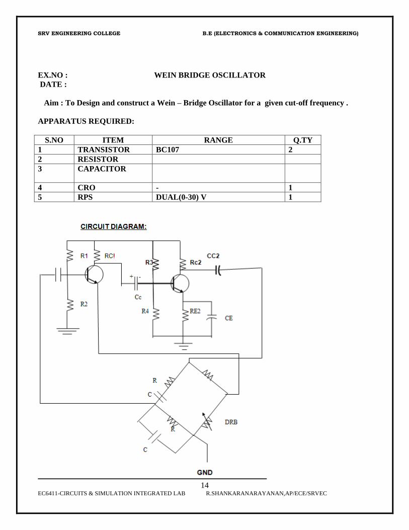
EX.NO : WEIN BRIDGE OSCILLATOR
DATE :
Aim : To Design and construct a Wein – Bridge Oscillator for a given cut-off frequency .
APPARATUS REQUIRED:
S.NO ITEM RANGE Q.TY
1 TRANSISTOR BC107 2
2 RESISTOR
3 CAPACITOR
4 CRO - 1
5 RPS DUAL(0-30) V 1
SRV ENGINEERING COLLEGE B.E (ELECTRONICS & COMMUNICATION ENGINEERING)
EC6411-CIRCUITS & SIMULATION INTEGRATED LAB R.SHANKARANARAYANAN,AP/ECE/SRVEC
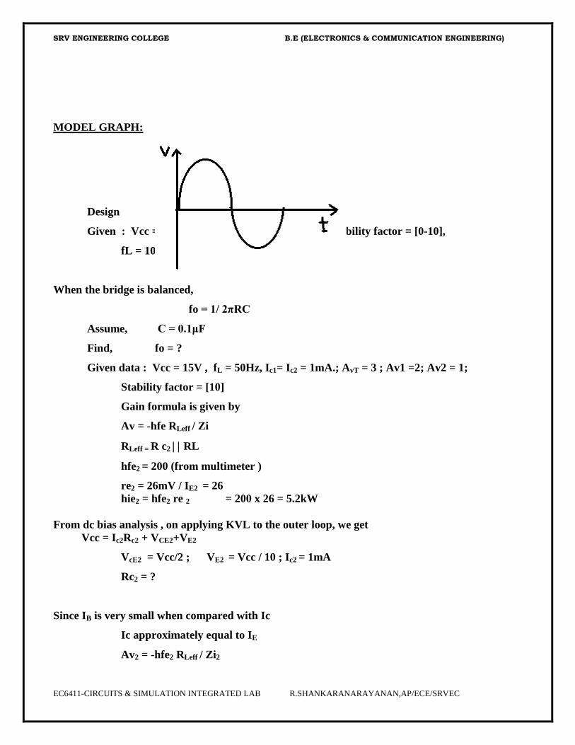
MODEL GRAPH:
Design
Given : Vcc = 12V , fo = 2 KHz, Ic1= Ic2 = 1mA.; Stability factor = [0-10],
fL = 100Hz
When the bridge is balanced,
fo = 1/ 2πRC
Assume, C = 0.1μF
Find, fo = ?
Given data : Vcc = 15V , fL = 50Hz, Ic1= Ic2 = 1mA.; AvT = 3 ; Av1 =2; Av2 = 1;
Stability factor = [10]
Gain formula is given by
Av = -hfe RLeff / Zi
RLeff = R c2 RL
hfe2 = 200 (from multimeter )
re2 = 26mV / IE2 = 26
hie2 = hfe2 re 2 = 200 x 26 = 5.2kW
From dc bias analysis , on applying KVL to the outer loop, we get
Vcc = Ic2Rc2 + VCE2+VE2
VcE2 = Vcc/2 ; VE2 = Vcc / 10 ; Ic2 = 1mA
Rc2 = ?
Since IB is very small when compared with Ic
Ic approximately equal to IE
Av2 = -hfe2 RLeff / Zi2

SRV ENGINEERING COLLEGE B.E (ELECTRONICS & COMMUNICATION ENGINEERING)
16 EC6411-CIRCUITS & SIMULATION INTEGRATED LAB R.SHANKARANARAYANAN,AP/ECE/SRVEC
Find RL|| Rc2 from above equation
Since Rc2 is known , Calculate RL.
VE2 = IE2RE2
Calculate RE2
S = 1+ RB2 / RE2
RB 2 =?
RB 2 =R3 || R4
VB2 = VCC . R4 / R3 + R4
VB2 = VBE2 + VE2
R3 =?
Find R4
Zi2 = (RB2 hie2 )
Zi2 = ?
Rleff1 = Zi2 Rc1
Find Rleff1 from the gain formula given above
Av1 = -hfe1 RLeff 1/ Zi1
RLeff1 = ?
On applying KVL to the first stage, we get
Vcc = Ic1 Rc1 + VCE1 +VE1
VCE1 = VCC / 2 ; VE1 = VCC / 10
Rc1 = ?
Find Ic1 approximately equal to IE1
R6 = RE1=?
S = 1+ RB1 / RE1
RB 1 =?
RB 1 =R1 || R2
VB1 = VCC . R2 / R1 + R2
VB1 = VBE2 +VE2
Find R1 = ?
Therefore find R2 = ?

SRV ENGINEERING COLLEGE B.E (ELECTRONICS & COMMUNICATION ENGINEERING)
EC6411-CIRCUITS & SIMULATION INTEGRATED LAB R.SHANKARANARAYANAN,AP/ECE/SRVEC
Zi1 = (RB1 hie1 )
R5 = RL – R6
Coupling and bypass capacitors can be thus found out.
Input coupling capacitor is given by , Xci = Z i / 10
Xci = 1/ 2f Ci
Ci = ?
output coupling capacitor is given by ,
X co=(Rc2 | | RL2) / 10
Xc0 = 1/ 2f Co
Co =?
By-pass capacitor is given by, XCE = RE2 / 10
XCE 1/ 2f CE2
CE =?
THEORY:
In wein bridge oscillator, wein bridge circuit is connected between the amplifier input
terminals and output terminals. The bridge has a series rc network in one arm and parallel
network in the adjoining arm. In the remaining 2 arms of the bridge resistors R1and Rf are
connected . To maintain oscillations total phase shift around the circuit must be zero and loop
gain unity. First condition occurs only when the bridge is balanced . Assuming that the resistors
and capacitors are equal in value, the resonant frequency of balanced bridge is given by
Fo = 0.159 RC
PROCEDURE:
1. The circuit is constructed as per the given circuit diagram.
2. Switch on the power supply and observe the output on the CRO( sine wave)
3. Note down the practical frequency and compare it with the theoretical frequency.
RESULT :
Theoritical Practical
Frequency f = 1 / 2 RC
SRV ENGINEERING COLLEGE B.E (ELECTRONICS & COMMUNICATION ENGINEERING)
18 EC6411-CIRCUITS & SIMULATION INTEGRATED LAB R.SHANKARANARAYANAN,AP/ECE/SRVEC
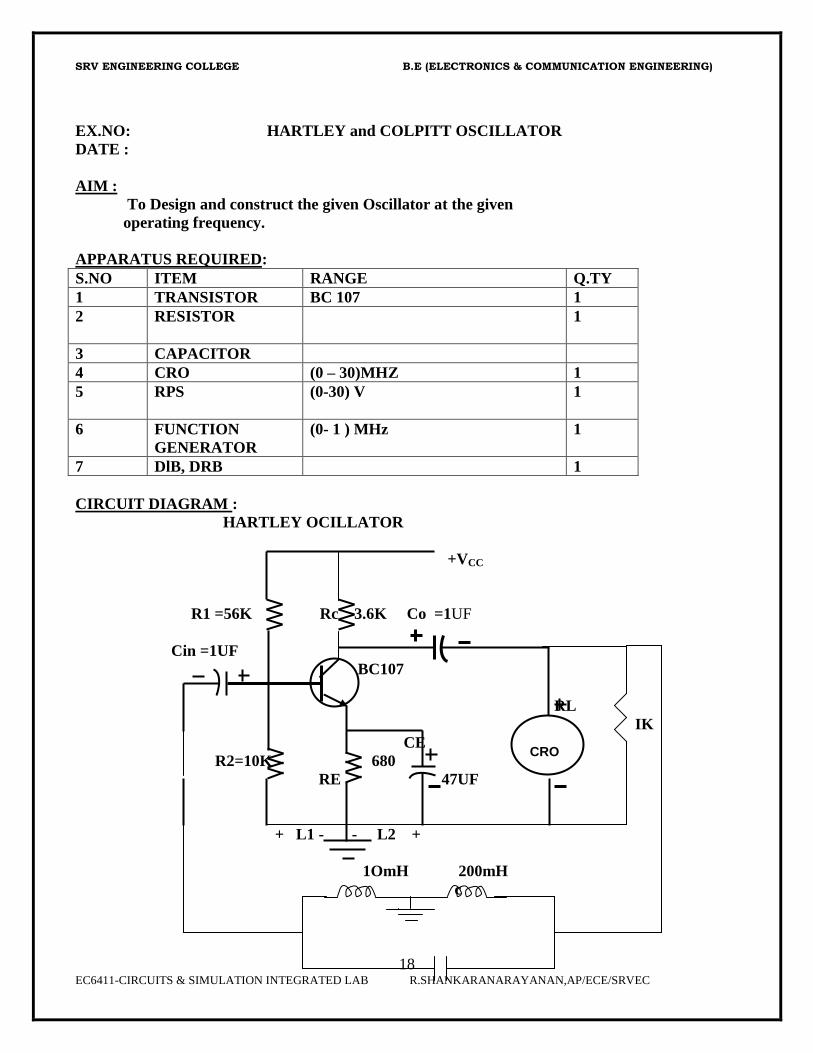
EX.NO: HARTLEY and COLPITT OSCILLATOR
DATE :
AIM :
To Design and construct the given Oscillator at the given
operating frequency.
APPARATUS REQUIRED:
S.NO ITEM RANGE Q.TY
1 TRANSISTOR BC 107 1
2 RESISTOR 1
3 CAPACITOR
4 CRO (0 – 30)MHZ 1
5
RPS (0-30) V 1
6 FUNCTION
GENERATOR
(0- 1 ) MHz 1
7 DlB, DRB 1
CIRCUIT DIAGRAM :
HARTLEY OCILLATOR
+VCC
R1 =56K Rc 3.6K Co =1UF
Cin =1UF
BC107
RL
IK
CE
R2=10K 680
RE 47UF
+ L1 - - L2 +
1OmH 200mH
c
CRO
SRV ENGINEERING COLLEGE B.E (ELECTRONICS & COMMUNICATION ENGINEERING)
EC6411-CIRCUITS & SIMULATION INTEGRATED LAB R.SHANKARANARAYANAN,AP/ECE/SRVEC
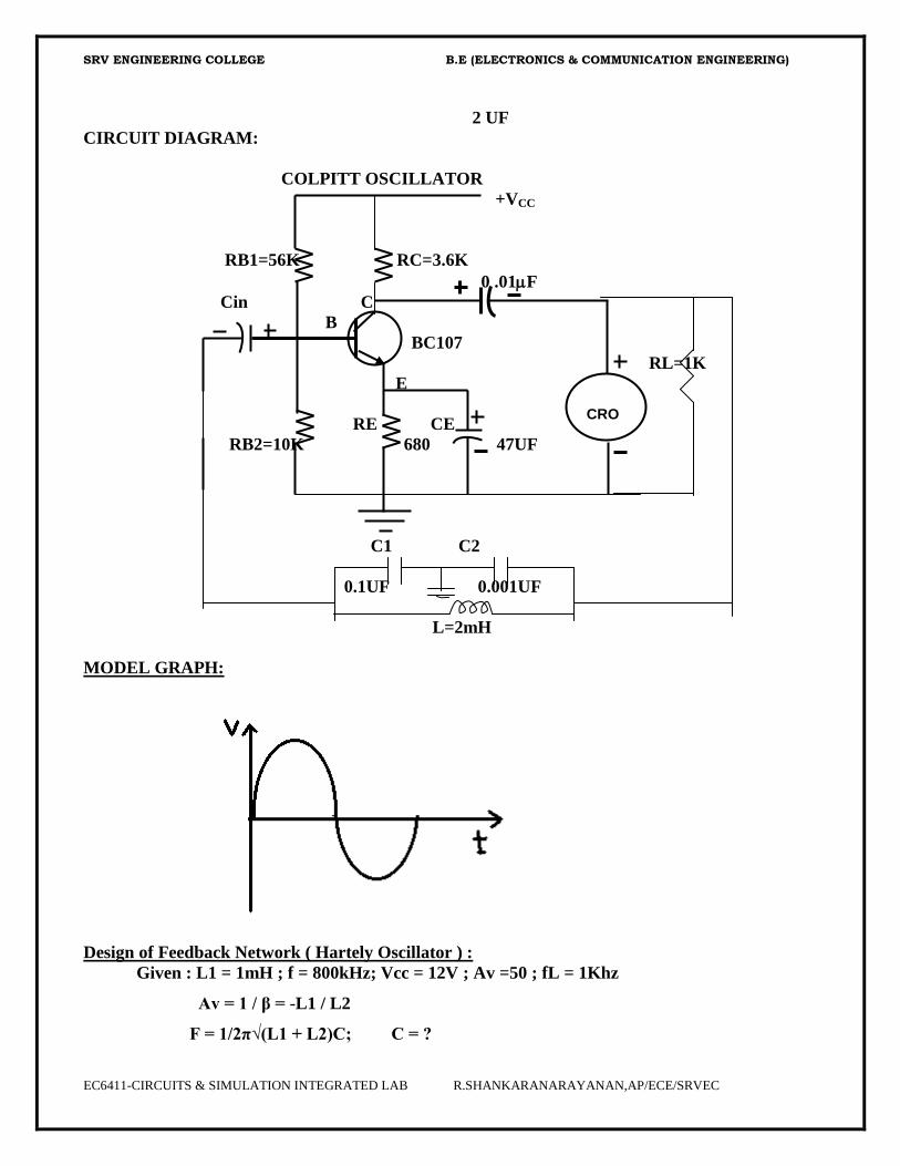
2 UF
CIRCUIT DIAGRAM:
COLPITT OSCILLATOR
+VCC
RB1=56K RC=3.6K
0 .01F
Cin C
B
BC107
RL=1K
E
RE CE
RB2=10K 680 47UF
C1 C2
0.1UF 0.001UF
L=2mH
MODEL GRAPH:
Design of Feedback Network ( Hartely Oscillator ) :
Given : L1 = 1mH ; f = 800kHz; Vcc = 12V ; Av =50 ; fL = 1Khz
Av = 1 / β = -L1 / L2
F = 1/2π√(L1 + L2)C; C = ?
CRO

SRV ENGINEERING COLLEGE B.E (ELECTRONICS & COMMUNICATION ENGINEERING)
20 EC6411-CIRCUITS & SIMULATION INTEGRATED LAB R.SHANKARANARAYANAN,AP/ECE/SRVEC
Design of Feedback Network ( Colpitt Oscillator ) :
Given : C1 = 0.1μF;f =800kHz; Vcc = 12V ; Av = 50 ; S = 10
IE = 5mA; fi = 1kHz
Av = Av = 1 / β = C2 / C1
f = 1/2π√(C1 + C2) / LC1C2
L = ?
Amplifier Design :
Gain formula is given by
Av = -hfe RLeff / hie ( Av = 29, design given )
Assume, VCE = Vcc / 2
RLeff = R c RL
re = 26mV / IE
hie = β re where re is internal resistance of the transistor.
hie = hfe re
VE = Vcc / 10
On applying KVL to output loop,
Vcc = IcRc + VCE + IERE
VE = IERE
Rc = ?;RL = ?
Since IB is very small when compared with Ic
Ic approximately equal to IE
RE = VE / IE = ?
VB = VBE + VE
VB = VCC . RB2 / RB1 + RB2
S = 1+ RB / RE
RB =?
RB = RB1 RB2
Find RB1 & RB2
Input Impedance, Zi = (RB hie )
Coupling and bypass capacitors can be thus found out.
Input coupling capacitor is given by , Xci = Z i / 10
Xci = 1/ 2f Ci

SRV ENGINEERING COLLEGE B.E (ELECTRONICS & COMMUNICATION ENGINEERING)
EC6411-CIRCUITS & SIMULATION INTEGRATED LAB R.SHANKARANARAYANAN,AP/ECE/SRVEC
Ci = ?
output coupling capacitor is given by ,
Xc0 = (Rc ׀׀RL) / 10
Xc0 = 1/ 2f Co
Co =?
By-pass capacitor is given by, XCE = RE / 10
XCE = 1/ 2f CE
CE =?
THEORY:
LC oscillator consisting of a tank circuit for generating sine wave of required
frequency. Rectifying Barkhausen criteria A for a circuit containing reactance A must
be positive and greater than or equal to unity.
PROCEDURE :
1. The circuit connection is made as per the circuit
diagram.
2. Switch on the power supply and observe the output
on the CRO(sine wave ).
3. Note down the practical frequency and compare it
with the theoretical frequency.
THEORETICAL FREQUENCY FOR HARTLEY OSCILLATOR:
THEORETICAL FREQUENCY FOR COLPITT OSCILLATOR:
fc = 1/2π√(C1 + C2) / LC1C2
PRACTICAL :
Observed Values:
Time Period =
Frequency =
RESULT :
Thus the LC oscillator is designed for the given frequency and the output response
is verified.
Theoritical Practical
Frequency Hartley
Colpitt
Hartley Colpitt
SRV ENGINEERING COLLEGE B.E (ELECTRONICS & COMMUNICATION ENGINEERING)
22 EC6411-CIRCUITS & SIMULATION INTEGRATED LAB R.SHANKARANARAYANAN,AP/ECE/SRVEC
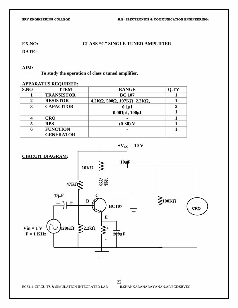
EX.NO: CLASS “C” SINGLE TUNED AMPLIFIER
DATE :
AIM:
To study the operation of class c tuned amplifier.
APPARATUS REQUIRED:
S.NO ITEM RANGE Q.TY
1 TRANSISTOR BC 107 1
2 RESISTOR 4.2K, 500, 197K, 2.2K, 1
3 CAPACITOR 0.1f
0.001f, 100f
2
1
4 CRO - 1
5 RPS (0-30) V 1
6 FUNCTION
GENERATOR
- 1
+VCC = 10 V
CIRCUIT DIAGRAM:
10F
10K
47K
47F C
B 100K
BC107
E
Vin = 1 V 120K 2.2k +
F = 1 KHz 100F
-
CRO

SRV ENGINEERING COLLEGE B.E (ELECTRONICS & COMMUNICATION ENGINEERING)
EC6411-CIRCUITS & SIMULATION INTEGRATED LAB R.SHANKARANARAYANAN,AP/ECE/SRVEC
MODEL GRAPH:
THEORY:
The amplifier is said to be class c amplifier if the Q Point and the input signal are selected such
that the output signal is obtained for less than a half cycle, for a full input cycle Due to such a
selection of the Q point, transistor remains active for less than a half cycle .Hence only that much
Part is reproduced at the output for remaining cycle of the input cycle the transistor remains cut
off and no signal is produced at the output .the total
Angle during which current flows is less than 180..This angle is called the conduction angle, Qc
PROCEDURE:
1.The connections are given as per the circuit diagram.
2. Connect the CRO in the output and trace the waveform.
3.calculate the practical frequency and compare with the
theoretical Frequency
4.plot the waveform obtained and calculate the bandwidth
RESULT:
Thus a class c single tuned amplifier was designed and its bandwidth is Calculated.
SRV ENGINEERING COLLEGE B.E (ELECTRONICS & COMMUNICATION ENGINEERING)
24 EC6411-CIRCUITS & SIMULATION INTEGRATED LAB R.SHANKARANARAYANAN,AP/ECE/SRVEC
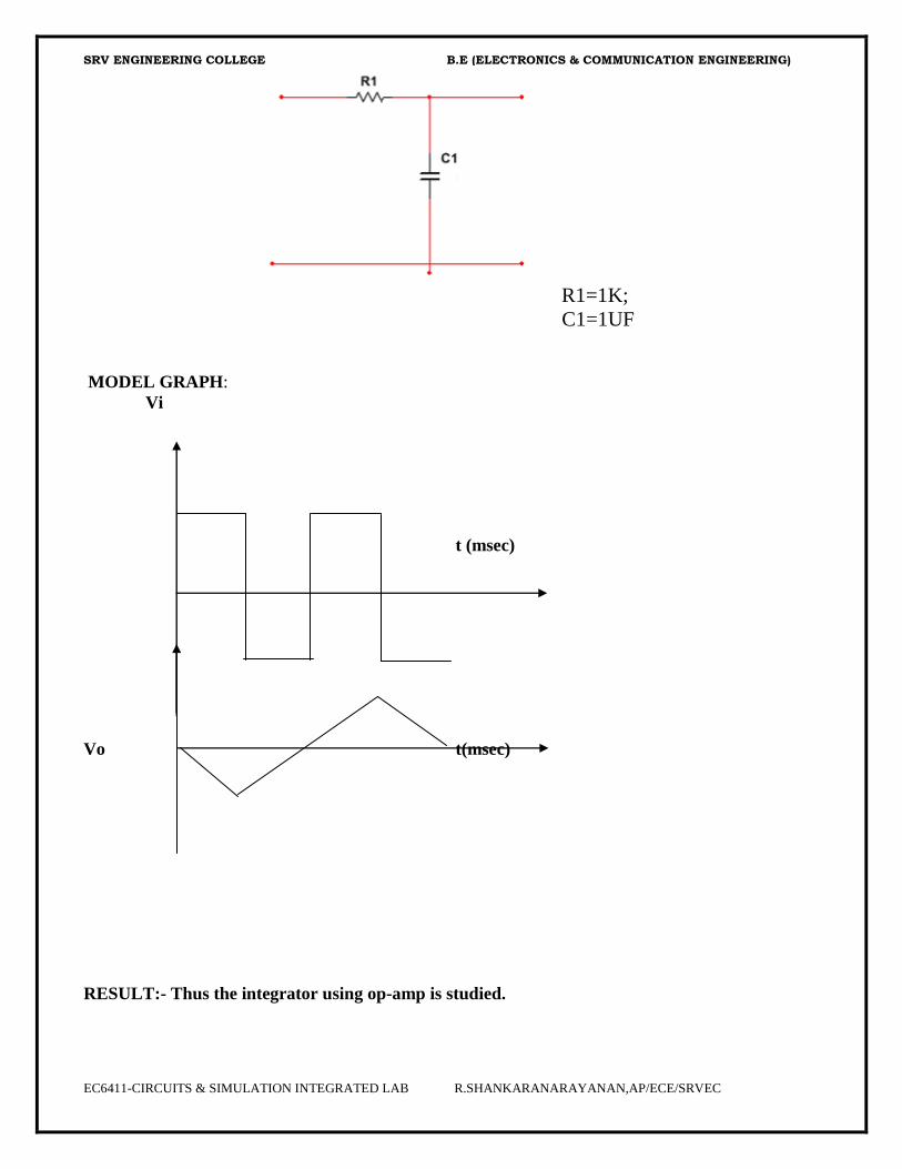
EX.NO: INTEGRATOR
DATE:
AIM:
To study the output waveform of integrator.
APPARATUS REQUIRED:
APPARATUS NAME RANGE QUANTITY
AUDIO OSCILLATOR
CRO
RESISTORS
CAPACITOR
OP-AMP
BREADBOARD
RPS
1K,10K
0.1F
IC741
1
1
1
1
1
THEORY:
A simple low pas RC circuit can also work as an integrator when time constant is very
large. This requires very large values of R and C.The components R and C cannot be made
infinitely large because of practical limitations. However in the op-amp integrator by MILLER‟s
theorem, the effective input capacitance becomes Cf (1-Av), where Av is the gain of the op-amp.
The gain Av is the infinite for an ideal op-amp, so the effective time constant of the opamp
integrator becomes very large which results perfect integration.
PROCEDURE:
1.Connections are given as per the circuit diagram.
2.The resistance Rcomp is also connected to the (+) input terminal
to minimize the effect of the input bias circuit.
3.It is noted that the gain of the integrator decreases with
increasing frequency.
4.Thus the integrator circuit does not have any high frequency
problem.
CIRCUIT DIAGRAM:
SRV ENGINEERING COLLEGE B.E (ELECTRONICS & COMMUNICATION ENGINEERING)
EC6411-CIRCUITS & SIMULATION INTEGRATED LAB R.SHANKARANARAYANAN,AP/ECE/SRVEC
R1=1K;
C1=1UF
MODEL GRAPH:
Vi
t (msec)
Vo t(msec)
RESULT:- Thus the integrator using op-amp is studied.
SRV ENGINEERING COLLEGE B.E (ELECTRONICS & COMMUNICATION ENGINEERING)
26 EC6411-CIRCUITS & SIMULATION INTEGRATED LAB R.SHANKARANARAYANAN,AP/ECE/SRVEC
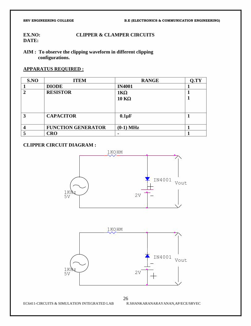
EX.NO: CLIPPER & CLAMPER CIRCUITS
DATE:
AIM : To observe the clipping waveform in different clipping
configurations.
APPARATUS REQUIRED :
S.NO ITEM RANGE Q.TY
1 DIODE IN4001 1
2 RESISTOR 1K
10 K
1
1
3 CAPACITOR 0.1µF
1
4 FUNCTION GENERATOR (0-1) MHz 1
5 CRO - 1
CLIPPER CIRCUIT DIAGRAM :
Vout
2V
IN4001
1KHz5V
1KOHM
IN4001
1KHz5V
1KOHM
2V
Vout
SRV ENGINEERING COLLEGE B.E (ELECTRONICS & COMMUNICATION ENGINEERING)
EC6411-CIRCUITS & SIMULATION INTEGRATED LAB R.SHANKARANARAYANAN,AP/ECE/SRVEC
Procedure :
1. Connections are given as per the circuit .
2. Set input signal voltage (5v,1kHz ) using function generator.
3. Observe the output waveform using CRO.
4. Sketch the observed waveform on the graph sheet.
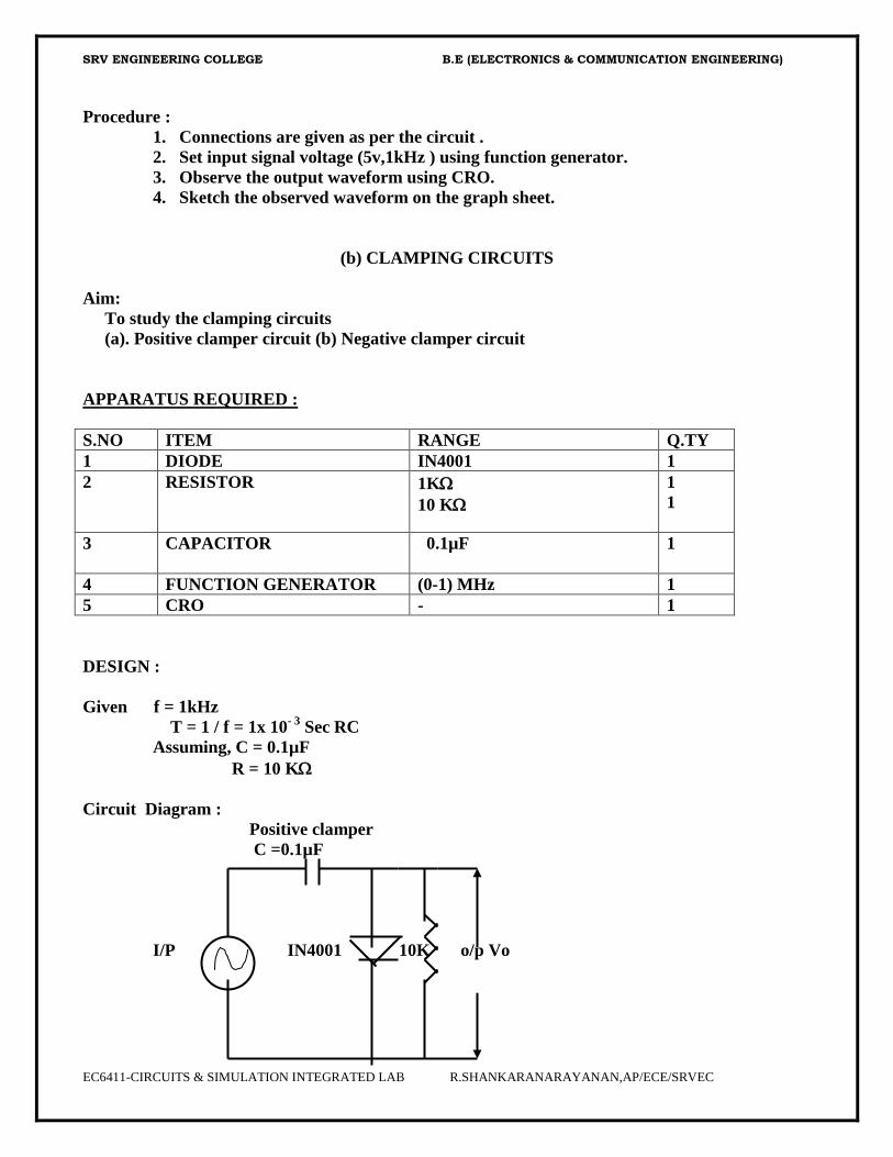
(b) CLAMPING CIRCUITS
Aim:
To study the clamping circuits
(a). Positive clamper circuit (b) Negative clamper circuit
APPARATUS REQUIRED :
S.NO ITEM RANGE Q.TY
1 DIODE IN4001 1
2 RESISTOR 1K
10 K
1
1
3 CAPACITOR 0.1µF
1
4 FUNCTION GENERATOR (0-1) MHz 1
5 CRO - 1
DESIGN :
Given f = 1kHz
T = 1 / f = 1x 10- 3
Sec RC
Assuming, C = 0.1µF
R = 10 K
Circuit Diagram :
Positive clamper
C =0.1µF
I/P IN4001 10K o/p Vo
SRV ENGINEERING COLLEGE B.E (ELECTRONICS & COMMUNICATION ENGINEERING)
28 EC6411-CIRCUITS & SIMULATION INTEGRATED LAB R.SHANKARANARAYANAN,AP/ECE/SRVEC
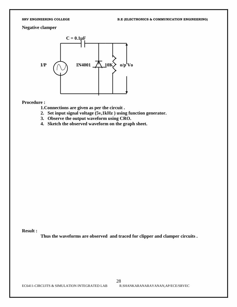
Negative clamper
C = 0.1µF
I/P IN4001 10K o/p Vo
Procedure :
1.Connections are given as per the circuit .
2. Set input signal voltage (5v,1kHz ) using function generator.
3. Observe the output waveform using CRO.
4. Sketch the observed waveform on the graph sheet.
Result :
Thus the waveforms are observed and traced for clipper and clamper circuits .
SRV ENGINEERING COLLEGE B.E (ELECTRONICS & COMMUNICATION ENGINEERING)
EC6411-CIRCUITS & SIMULATION INTEGRATED LAB R.SHANKARANARAYANAN,AP/ECE/SRVEC
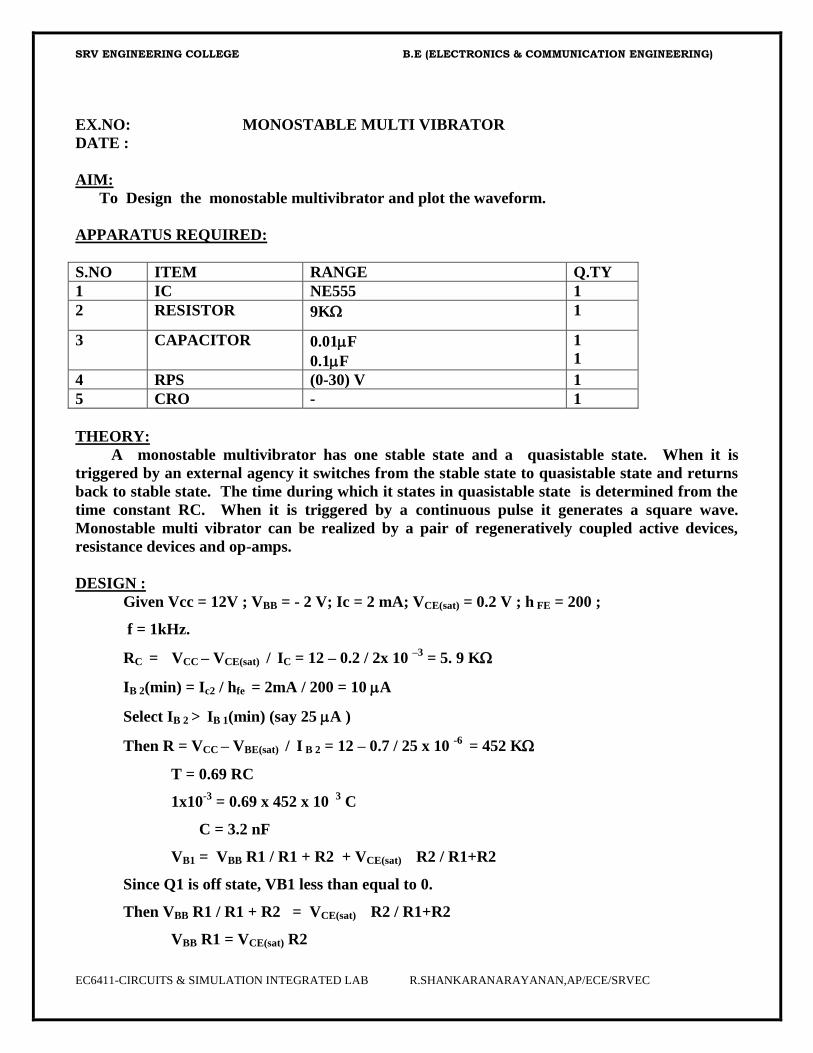
EX.NO: MONOSTABLE MULTI VIBRATOR
DATE :
AIM:
To Design the monostable multivibrator and plot the waveform.
APPARATUS REQUIRED:
S.NO ITEM RANGE Q.TY
1 IC NE555 1
2 RESISTOR 9K 1
3 CAPACITOR 0.01F
0.1F
1
1
4 RPS (0-30) V 1
5 CRO - 1
THEORY:
A monostable multivibrator has one stable state and a quasistable state. When it is
triggered by an external agency it switches from the stable state to quasistable state and returns
back to stable state. The time during which it states in quasistable state is determined from the
time constant RC. When it is triggered by a continuous pulse it generates a square wave.
Monostable multi vibrator can be realized by a pair of regeneratively coupled active devices,
resistance devices and op-amps.
DESIGN :
Given Vcc = 12V ; VBB = - 2 V; Ic = 2 mA; VCE(sat) = 0.2 V ; h FE = 200 ;
f = 1kHz.
RC = VCC – VCE(sat) / IC = 12 – 0.2 / 2x 10 –3
= 5. 9 K
IB 2(min) = Ic2 / hfe = 2mA / 200 = 10 A
Select IB 2 > IB 1(min) (say 25 A )
Then R = VCC – VBE(sat) / I B 2 = 12 – 0.7 / 25 x 10 -6
= 452 K
T = 0.69 RC
1x10-3
= 0.69 x 452 x 10 3
C
C = 3.2 nF
VB1 = VBB R1 / R1 + R2 + VCE(sat) R2 / R1+R2
Since Q1 is off state, VB1 less than equal to 0.
Then VBB R1 / R1 + R2 = VCE(sat) R2 / R1+R2
VBB R1 = VCE(sat) R2

SRV ENGINEERING COLLEGE B.E (ELECTRONICS & COMMUNICATION ENGINEERING)
30 EC6411-CIRCUITS & SIMULATION INTEGRATED LAB R.SHANKARANARAYANAN,AP/ECE/SRVEC
2R1 = 0.2R2
Assume R1 = 10 K. Then R2 = 100 K
C1 = 25pF( Commutative capacitor )
procedure :
1. Connect the circuit as per circuit diagram.
2. Switch on the regulated power supply and observe the output waveform at
the collector of Q1 and Q2 and plot it.
3. Trigger the monostable multivibrator with a pulse and observe the change in
waveform.
4. Plot the waveform and observe the changes before and after triggering the input to the
circuit.
CIRCUIT DIAGRAM :
+ VCC = +12v
5.9K 452k 5.9k
10k
3.2nf
22pf
C C
B B
Vo1 BC107 BC107 VO2
E 100k E
-VBB

SRV ENGINEERING COLLEGE B.E (ELECTRONICS & COMMUNICATION ENGINEERING)
EC6411-CIRCUITS & SIMULATION INTEGRATED LAB R.SHANKARANARAYANAN,AP/ECE/SRVEC
PROCEDURE:
The connections are made as per the diagram. The value of R is chosen as 9k. The DCB
is set to the designed value. The power supply is switched on and set to +5V.
The output of the pulse generator is set to the desired frequency. Here the frequency of
triggering should be greater than width of ON period (i.e.) T >W. The output is observed using
CRO and the result is compared with the theoretical value. The experiment can be repeated for
different values of C and the results are tabulated.
OBSERVATION
C (uf)
Theoritical(T=1.095 RC(ms)))
Practical T(ms)
RESULT: Thus the monostable multivibrator is designed and its output waveform is traced.
SRV ENGINEERING COLLEGE B.E (ELECTRONICS & COMMUNICATION ENGINEERING)
32 EC6411-CIRCUITS & SIMULATION INTEGRATED LAB R.SHANKARANARAYANAN,AP/ECE/SRVEC
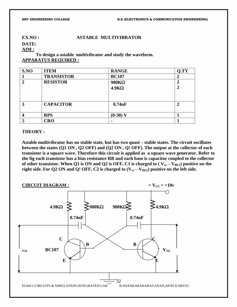
EX.NO : ASTABLE MULTIVIBRATOR
DATE:
AIM :
To design a astable multivibrator and study the waveform.
APPARATUS REQUIRED :
S.NO ITEM RANGE Q.TY
1 TRANSISTOR BC107 2
2 RESISTOR 980K
4.9K
2
2
3 CAPACITOR 0.74nF
2
4 RPS (0-30) V 1
5 CRO - 1
THEORY :
Astable multivibrator has no stable state, but has two quasi – stable states. The circuit oscillates
between the states (Q1 ON , Q2 OFF) and (Q2 ON , Q! OFF). The output at the collector of each
transistor is a square wave. Therefore this circuit is applied as a square wave generator. Refer to
the fig each transistor has a bias resistance RB and each base is capacitor coupled to the collector
of other transistor. When Q1 is ON and Q2 is OFF, C1 is charged to ( Vcc – VBE1) positive on the
right side. For Q2 ON and Q! OFF, C2 is charged to (Vcc – VBE2) positive on the left side.
CIRCUIT DIAGRAM : + VCC = +10v
4.9K 980K 980K 4.9K
0.74nF 0.74nF
C C
B B
Vo1 BC107 BC107 VO2
E E
SRV ENGINEERING COLLEGE B.E (ELECTRONICS & COMMUNICATION ENGINEERING)
EC6411-CIRCUITS & SIMULATION INTEGRATED LAB R.SHANKARANARAYANAN,AP/ECE/SRVEC
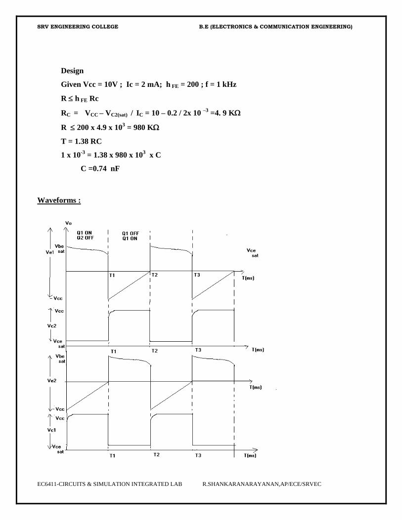
Design
Given Vcc = 10V ; Ic = 2 mA; h FE = 200 ; f = 1 kHz
R h FE Rc
RC = VCC – VC2(sat) / IC = 10 – 0.2 / 2x 10 –3
=4. 9 K
R 200 x 4.9 x 103 = 980 K
T = 1.38 RC
1 x 10-3
= 1.38 x 980 x 103 x C
C =0.74 nF
Waveforms :

SRV ENGINEERING COLLEGE B.E (ELECTRONICS & COMMUNICATION ENGINEERING)
34 EC6411-CIRCUITS & SIMULATION INTEGRATED LAB R.SHANKARANARAYANAN,AP/ECE/SRVEC
PROCEDURE :
1. The connections are given as per the circuit diagram.
2. Switch on the power supply.
3. Observe the waveform both at bases andcollectors of Q1 and Q2.
4. Connect the CRO in the output of Q1 and Q2 and trace the square waveform.
RESULT :
Thus the square wave forms are generated using astable multivibrator.
SRV ENGINEERING COLLEGE B.E (ELECTRONICS & COMMUNICATION ENGINEERING)
EC6411-CIRCUITS & SIMULATION INTEGRATED LAB R.SHANKARANARAYANAN,AP/ECE/SRVEC
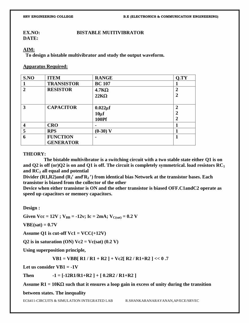
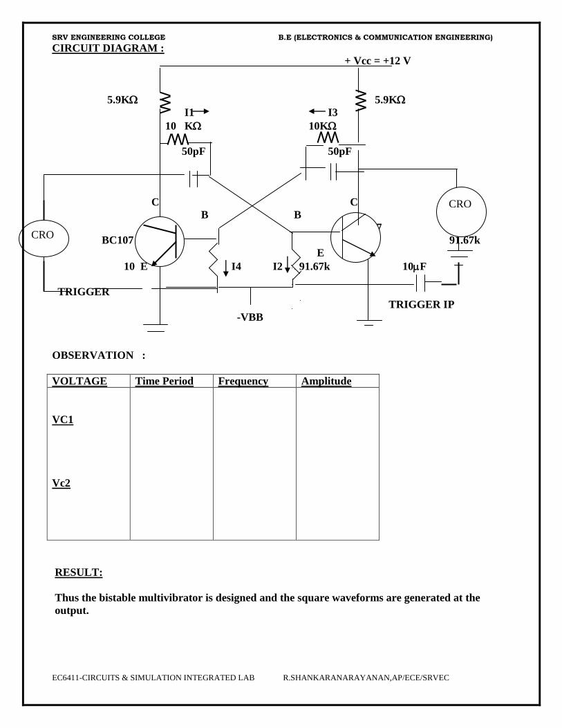
EX.NO: BISTABLE MUITIVIBRATOR
DATE:
AIM:
To design a bistable multivibrator and study the output waveform.
Apparatus Required:
S.NO ITEM RANGE Q.TY
1 TRANSISTOR BC 107 1
2 RESISTOR 4.7K
22K
2
2
3 CAPACITOR 0.022f
10f
100Pf
2
2
2
4 CRO - 1
5 RPS (0-30) V 1
6 FUNCTION
GENERATOR
- 1
THEORY:
The bistable multivibrator is a switching circuit with a two stable state either Q1 is on
and Q2 is off (or)Q2 is on and Q1 is off. The circuit is completely symmetrical. load resistors RC1
and RC2 all equal and potential
Divider (R1,R2)and (R1 andR2 ) from identical bias Network at the transistor bases. Each
transistor is biased from the collector of the other
Device when either transistor is ON and the other transistor is biased OFF.C1andC2 operate as
speed up capacitors or memory capacitors.
Design :
Given Vcc = 12V ; VBB = -12v; Ic = 2mA; VC(sat) = 0.2 V
VBE(sat) = 0.7V
Assume Q1 is cut-off Vc1 = VCC(+12V)
Q2 is in saturation (ON) Vc2 = Vc(sat) (0.2 V)
Using superposition principle,
VB1 = VBB[ R1 / R1 + R2 ] + Vc2[ R2 / R1+R2 ] << 0 .7
Let us consider VB1 = -1V
Then -1 = [-12R1/R1+R2 ] + [ 0.2R2 / R1+R2 ]
Assume R1 = 10K such that it ensures a loop gain in excess of unity during the transition
between states. The inequality

SRV ENGINEERING COLLEGE B.E (ELECTRONICS & COMMUNICATION ENGINEERING)
36 EC6411-CIRCUITS & SIMULATION INTEGRATED LAB R.SHANKARANARAYANAN,AP/ECE/SRVEC
R1 < hfe Rc
R2 = 91.67 K
Test for conditions : Q1 = cut-off (Vc1 = 12V )
Q2 = Saturation / (ON) (VC2 = 0.2V)
Minimum base current, IB (min) must be less than the base current (IB) i.e.,
IB (min) < IB
Calculate hfe from multimeter (say = 200)
IB 2(min) = Ic2 / hfe
Ic2 = Ic – I3
Ic2 = ( 2 – 0.12 )mA = 1.88 mA
IB 2(min) = 1.88mA / 200 = 9.4 A
IB 2 = I1 – I2
IB 2 = (0.71 – 0.14 )mA = 0.57 mA
Since IB 2 > IB 2(min) ,Q2 is ON
C1 = 25 pF ( Commutative capacitor )
IC = VCC – Vc2 / RC
RC = VCC – Vc2 / IC = 12 – 0.2 / 2x 10 –3
= 5.9 K
I3 = Vc2 - VBB / R1 + R2 = 0.2 + 12 / ( 10 + 91.6 )K = 0.12mA
I1 = Vc1 - VBE / RC + R1 = 12 – 0.7 / ( 5.9 + 10 ) K = 0.71mA
I2 = VBE - VBB / R2 = 0.7 + 12 / 91.6K = 0.14 mA
Procedure :
1. Connect the cir cuit as per circuit diagram.
2. Switch on the regulated power supply and observe the output waveform at the
collector of Q1 and Q2.
3. Sketch the waveform.
4. Apply a threshold voltage and observe the change of states of Q1 and Q2.
5. Sketch the waveform.
SRV ENGINEERING COLLEGE B.E (ELECTRONICS & COMMUNICATION ENGINEERING)
EC6411-CIRCUITS & SIMULATION INTEGRATED LAB R.SHANKARANARAYANAN,AP/ECE/SRVEC
CIRCUIT DIAGRAM :
+ Vcc = +12 V
5.9K 5.9K
I1 I3
10 K 10K
50pF 50pF
C C
B B
BC107
22 BC107 91.67k
E
10 E I4 I2 91.67k 10F
TRIGGER
TRIGGER IP
-VBB
OBSERVATION :
VOLTAGE Time Period Frequency Amplitude
VC1
Vc2
RESULT:
Thus the bistable multivibrator is designed and the square waveforms are generated at the
output.
CRO
CRO

SRV ENGINEERING COLLEGE B.E (ELECTRONICS & COMMUNICATION ENGINEERING)
38 EC6411-CIRCUITS & SIMULATION INTEGRATED LAB R.SHANKARANARAYANAN,AP/ECE/SRVEC
SIMULATION LAB
GUIDELINES FOR DESIGNING CIRCUITS IN MULTISIM
Same procedure is for MULTISIM also only slight variations to choose components and
project title. comparing with ORCAD ,MULTISIM is user friendly software to design
circuits.
Step 1 : Open MULTISIM Software
Step 2: MULTISIM main window
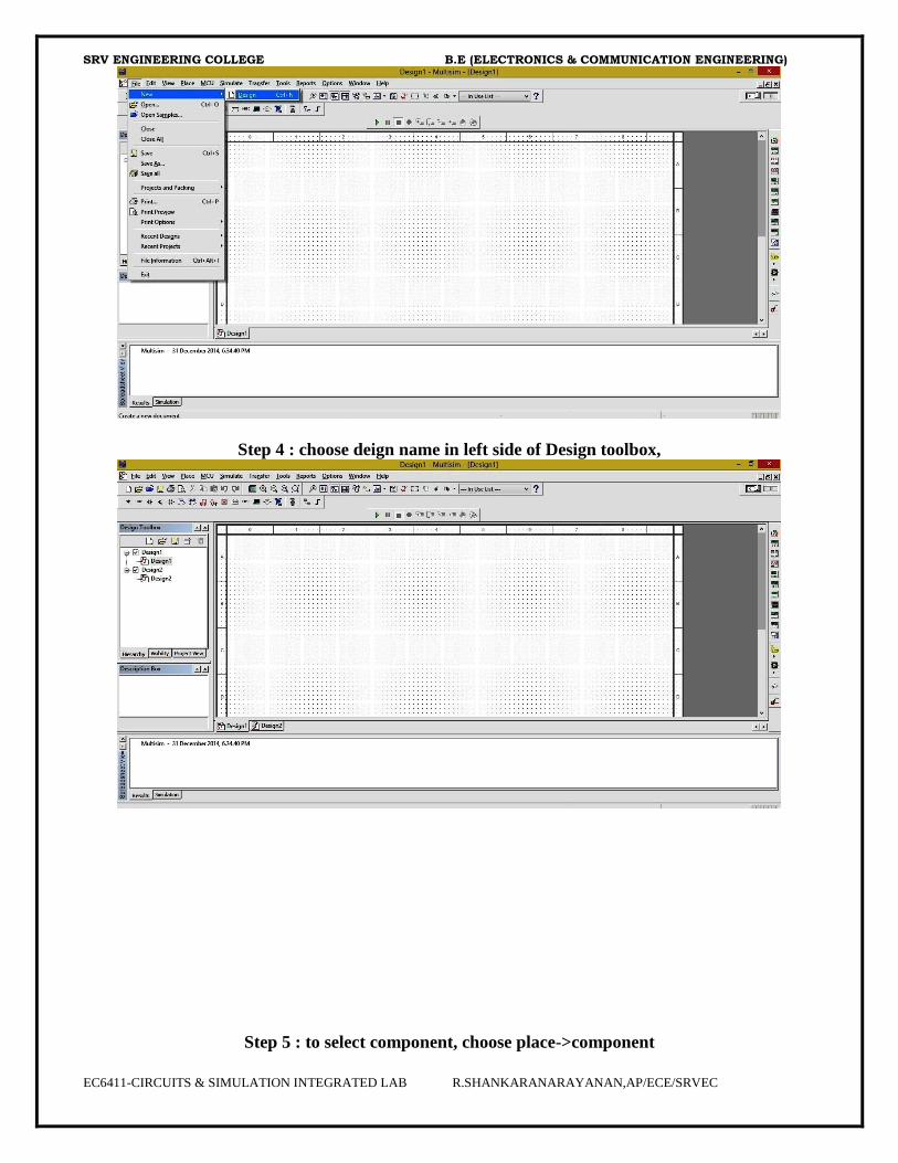
Step 3: Choose File menu ->new->Design
SRV ENGINEERING COLLEGE B.E (ELECTRONICS & COMMUNICATION ENGINEERING)
EC6411-CIRCUITS & SIMULATION INTEGRATED LAB R.SHANKARANARAYANAN,AP/ECE/SRVEC
Step 4 : choose deign name in left side of Design toolbox,
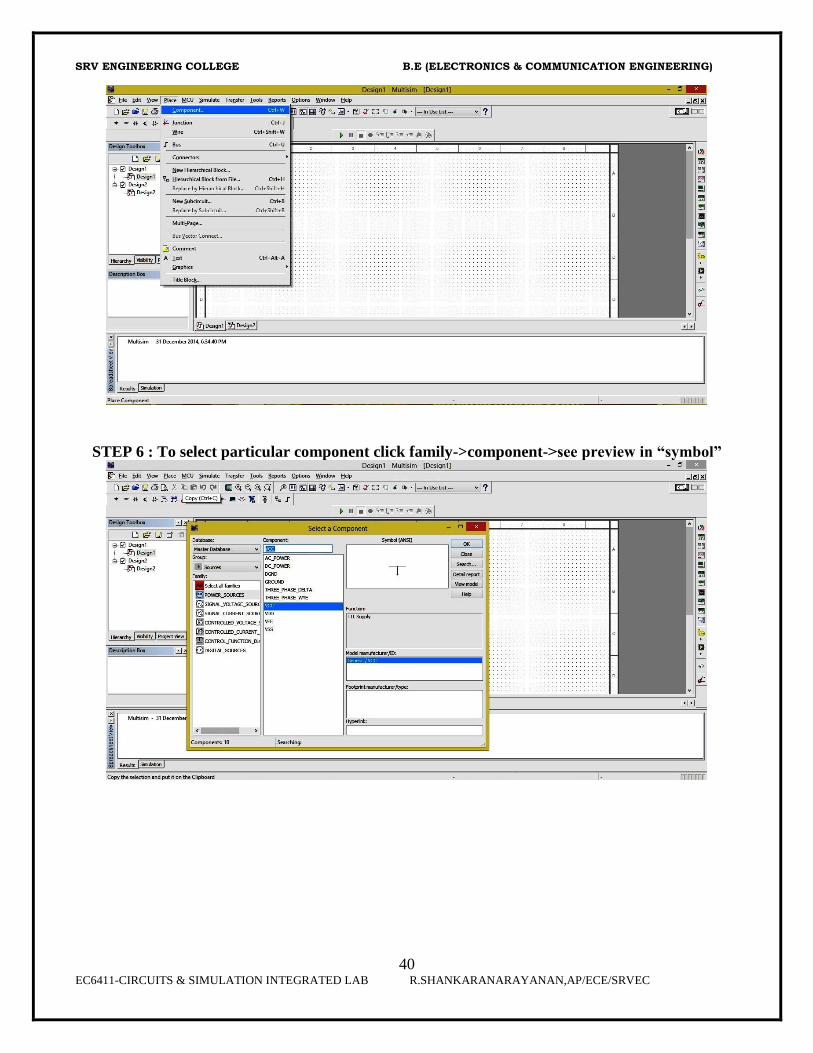
Step 5 : to select component, choose place->component
SRV ENGINEERING COLLEGE B.E (ELECTRONICS & COMMUNICATION ENGINEERING)
40 EC6411-CIRCUITS & SIMULATION INTEGRATED LAB R.SHANKARANARAYANAN,AP/ECE/SRVEC
STEP 6 : To select particular component click family->component->see preview in “symbol”

SRV ENGINEERING COLLEGE B.E (ELECTRONICS & COMMUNICATION ENGINEERING)
EC6411-CIRCUITS & SIMULATION INTEGRATED LAB R.SHANKARANARAYANAN,AP/ECE/SRVEC
Step 7 : after selecting component ( ex VCC), place part in PCB layout design,
Step 8 : To select BJT transistor, choose “Groups”->click “BJT _NPN” in family->choose model
in “component” and confirm it in “symbol” preview
SRV ENGINEERING COLLEGE B.E (ELECTRONICS & COMMUNICATION ENGINEERING)
42 EC6411-CIRCUITS & SIMULATION INTEGRATED LAB R.SHANKARANARAYANAN,AP/ECE/SRVEC
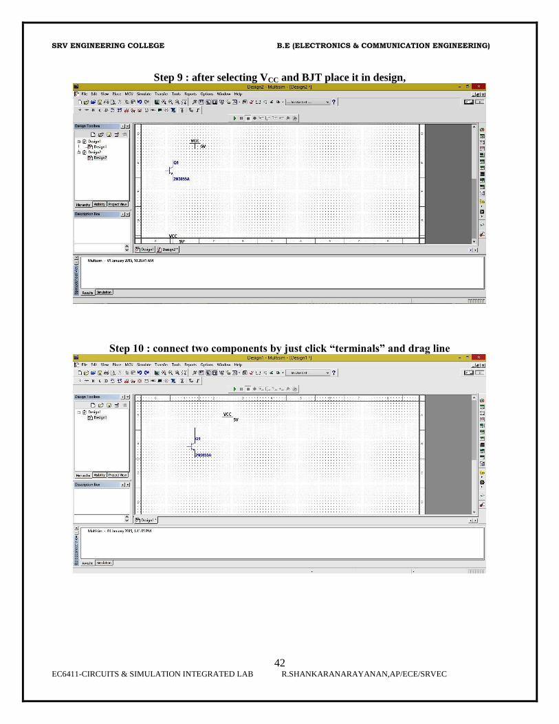
Step 9 : after selecting VCC and BJT place it in design,
Step 10 : connect two components by just click “terminals” and drag line
SRV ENGINEERING COLLEGE B.E (ELECTRONICS & COMMUNICATION ENGINEERING)
EC6411-CIRCUITS & SIMULATION INTEGRATED LAB R.SHANKARANARAYANAN,AP/ECE/SRVEC
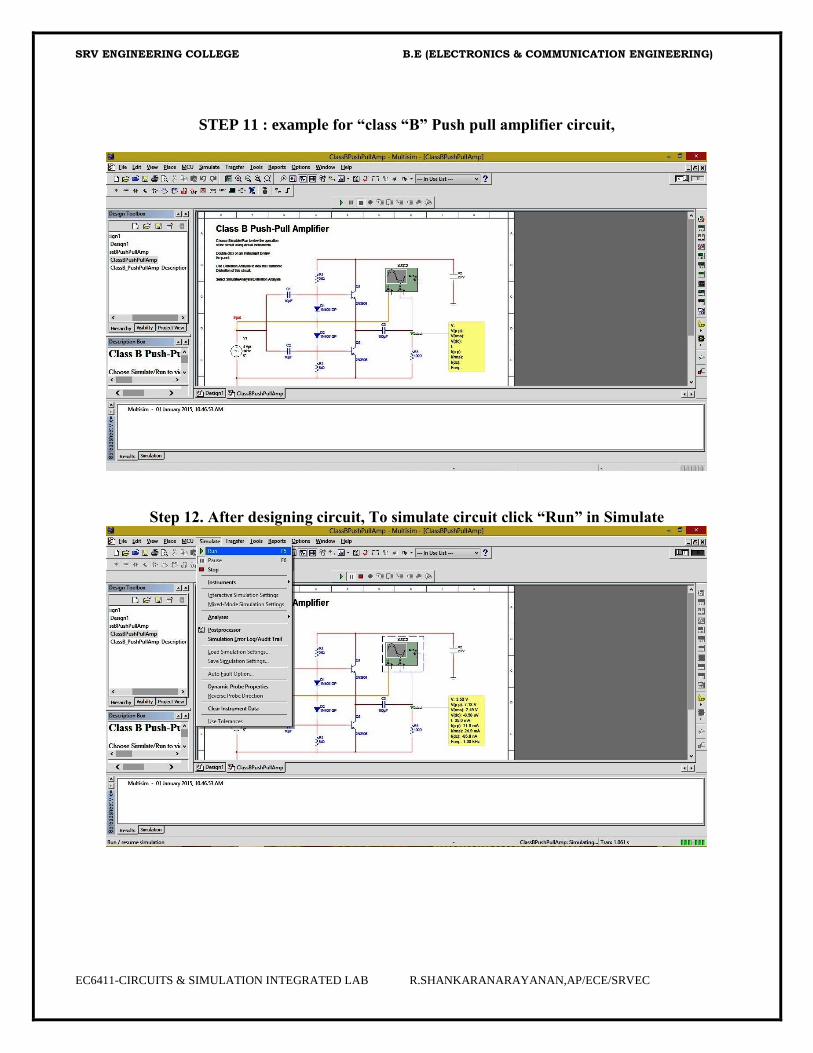
STEP 11 : example for “class “B” Push pull amplifier circuit,
Step 12. After designing circuit, To simulate circuit click “Run” in Simulate
SRV ENGINEERING COLLEGE B.E (ELECTRONICS & COMMUNICATION ENGINEERING)
44 EC6411-CIRCUITS & SIMULATION INTEGRATED LAB R.SHANKARANARAYANAN,AP/ECE/SRVEC
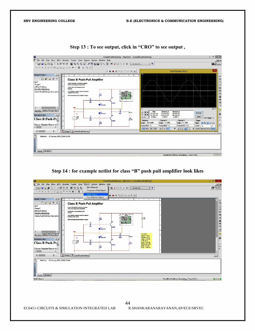
Step 13 : To see output, click in “CRO” to see output ,
Step 14 : for example netlist for class “B” push pull amplifier look likes

SRV ENGINEERING COLLEGE B.E (ELECTRONICS & COMMUNICATION ENGINEERING)
EC6411-CIRCUITS & SIMULATION INTEGRATED LAB R.SHANKARANARAYANAN,AP/ECE/SRVEC
Step 15 : You can run circuit by design „NETLIST‟ in report option,to see netlist click “reports”-
netlist

SRV ENGINEERING COLLEGE B.E (ELECTRONICS & COMMUNICATION ENGINEERING)
46 EC6411-CIRCUITS & SIMULATION INTEGRATED LAB R.SHANKARANARAYANAN,AP/ECE/SRVEC
GUIDELINES FOR DESIGNING CIRCUITS IN PSPICE
Step 1 : Open ORCAD PSPICE Software
Step 2: ORCAD main window
SRV ENGINEERING COLLEGE B.E (ELECTRONICS & COMMUNICATION ENGINEERING)
EC6411-CIRCUITS & SIMULATION INTEGRATED LAB R.SHANKARANARAYANAN,AP/ECE/SRVEC
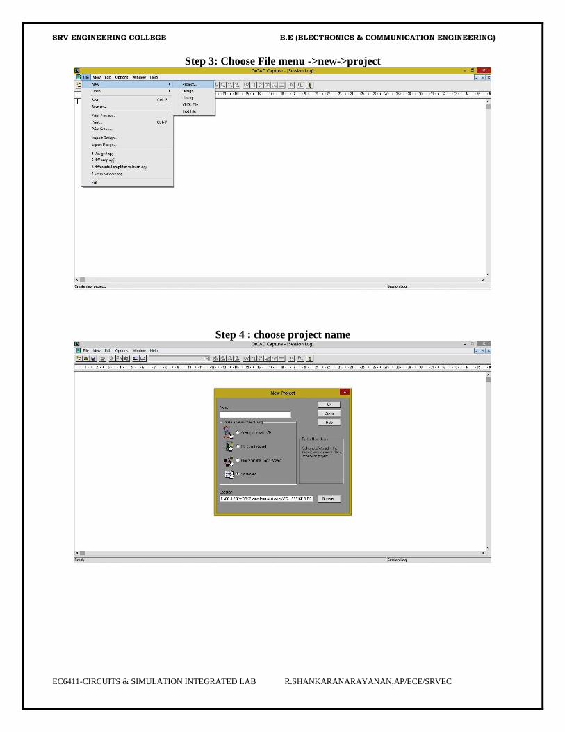
Step 3: Choose File menu ->new->project
Step 4 : choose project name
SRV ENGINEERING COLLEGE B.E (ELECTRONICS & COMMUNICATION ENGINEERING)
48 EC6411-CIRCUITS & SIMULATION INTEGRATED LAB R.SHANKARANARAYANAN,AP/ECE/SRVEC
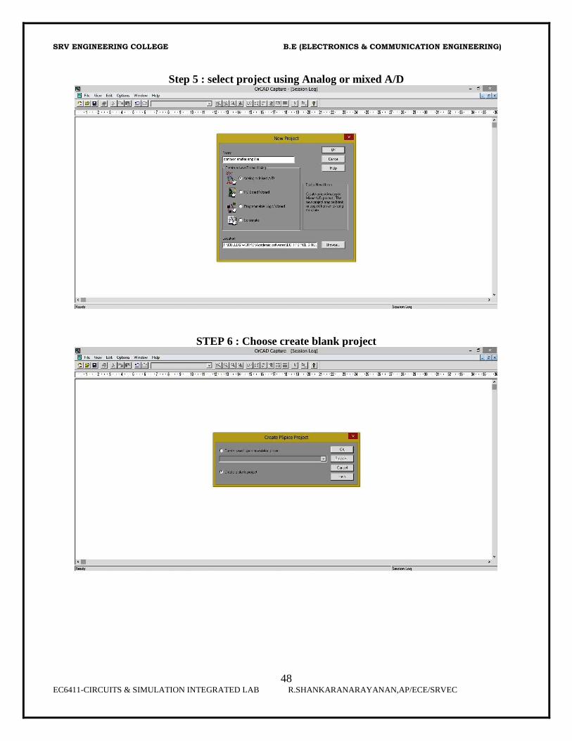
Step 5 : select project using Analog or mixed A/D
STEP 6 : Choose create blank project
SRV ENGINEERING COLLEGE B.E (ELECTRONICS & COMMUNICATION ENGINEERING)
EC6411-CIRCUITS & SIMULATION INTEGRATED LAB R.SHANKARANARAYANAN,AP/ECE/SRVEC
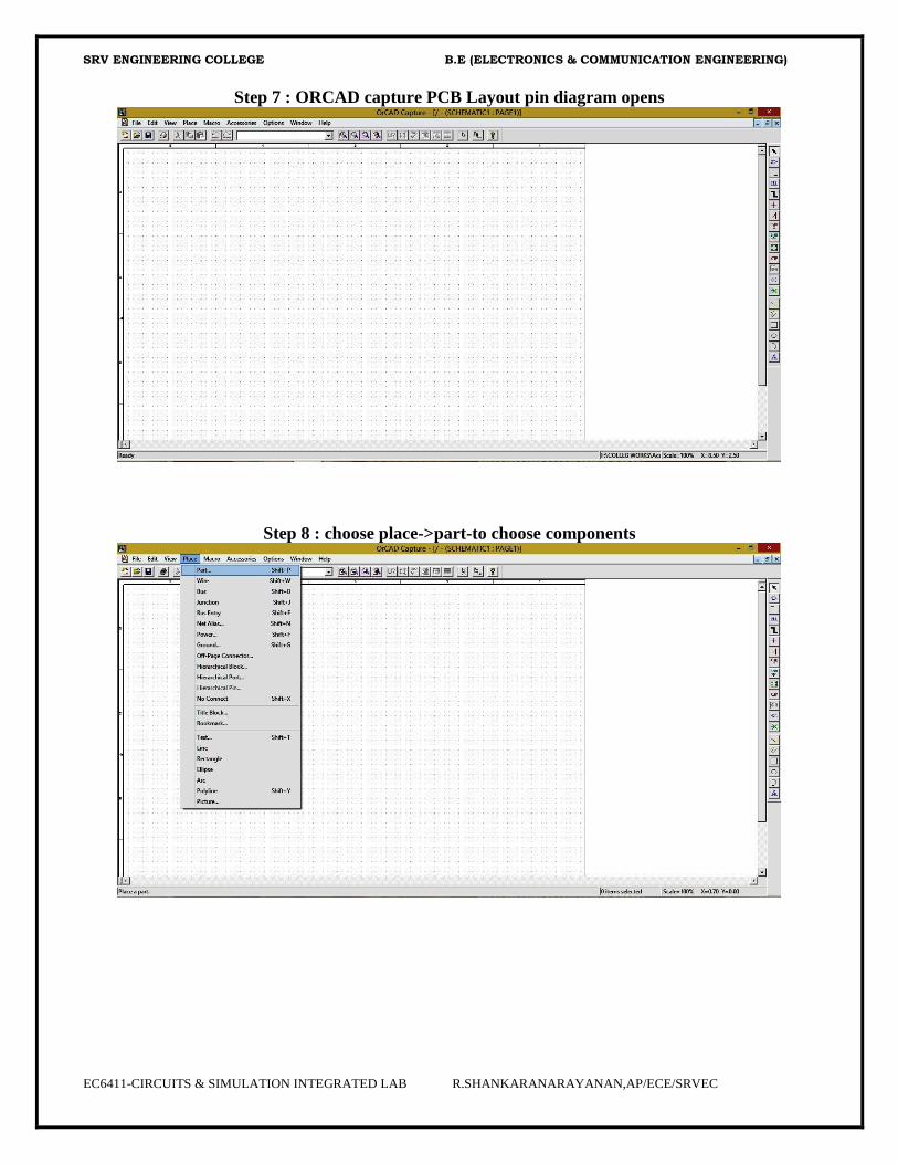
Step 7 : ORCAD capture PCB Layout pin diagram opens
Step 8 : choose place->part-to choose components
SRV ENGINEERING COLLEGE B.E (ELECTRONICS & COMMUNICATION ENGINEERING)
50 EC6411-CIRCUITS & SIMULATION INTEGRATED LAB R.SHANKARANARAYANAN,AP/ECE/SRVEC
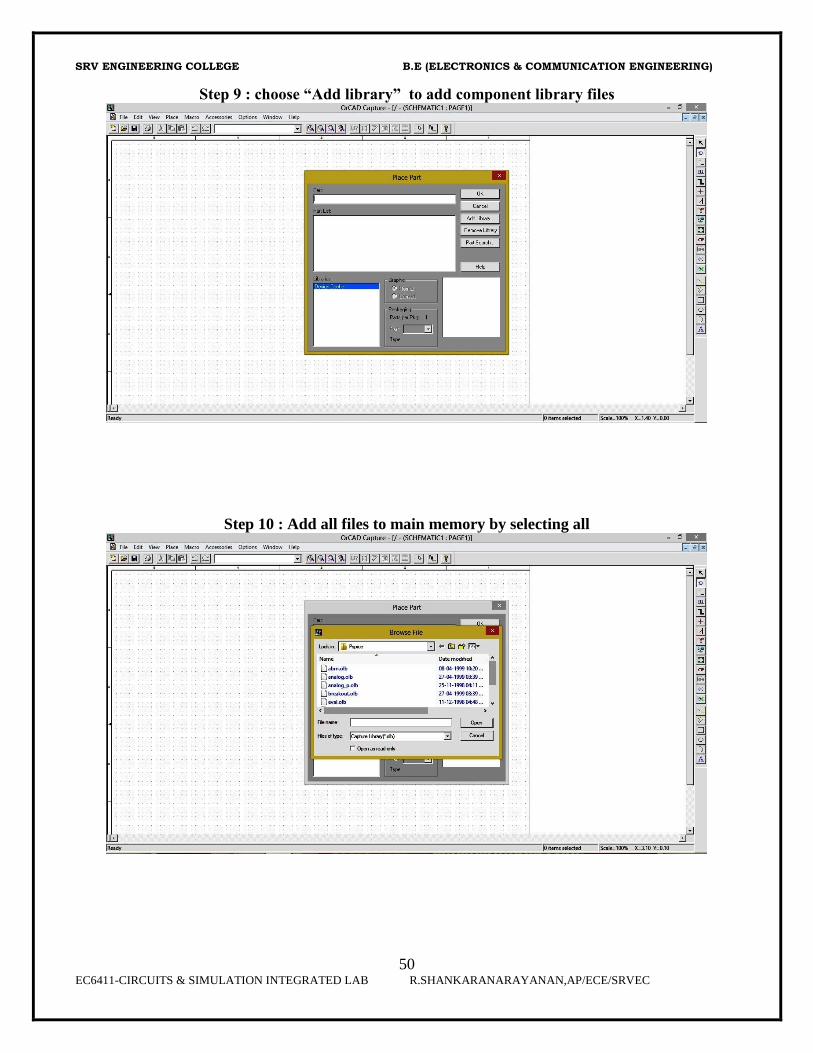
Step 9 : choose “Add library” to add component library files
Step 10 : Add all files to main memory by selecting all
SRV ENGINEERING COLLEGE B.E (ELECTRONICS & COMMUNICATION ENGINEERING)
EC6411-CIRCUITS & SIMULATION INTEGRATED LAB R.SHANKARANARAYANAN,AP/ECE/SRVEC
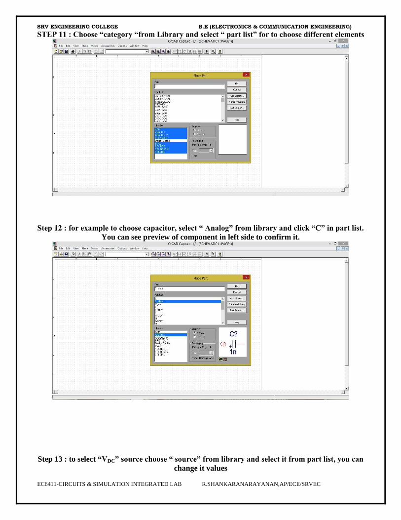
STEP 11 : Choose “category “from Library and select “ part list” for to choose different elements
Step 12 : for example to choose capacitor, select “ Analog” from library and click “C” in part list.
You can see preview of component in left side to confirm it.
Step 13 : to select “VDC” source choose “ source” from library and select it from part list, you can
change it values
SRV ENGINEERING COLLEGE B.E (ELECTRONICS & COMMUNICATION ENGINEERING)
52 EC6411-CIRCUITS & SIMULATION INTEGRATED LAB R.SHANKARANARAYANAN,AP/ECE/SRVEC
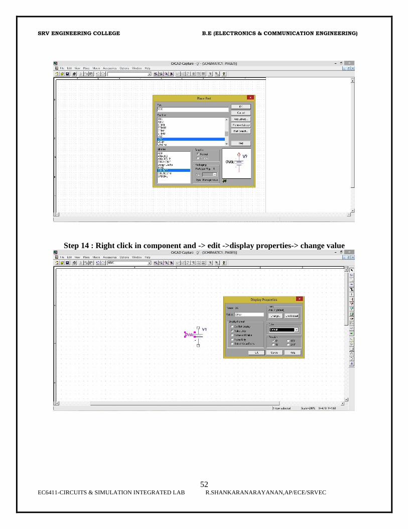
Step 14 : Right click in component and -> edit ->display properties-> change value
SRV ENGINEERING COLLEGE B.E (ELECTRONICS & COMMUNICATION ENGINEERING)
EC6411-CIRCUITS & SIMULATION INTEGRATED LAB R.SHANKARANARAYANAN,AP/ECE/SRVEC
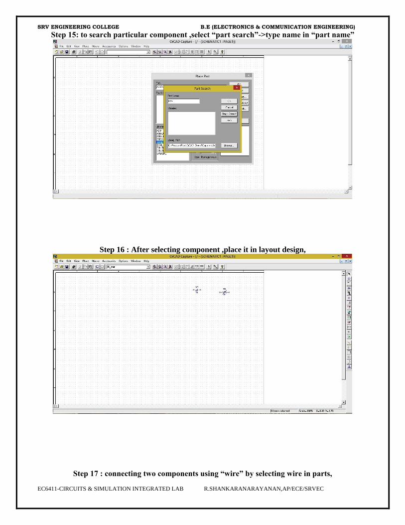
Step 15: to search particular component ,select “part search”->type name in “part name”
Step 16 : After selecting component ,place it in layout design,
Step 17 : connecting two components using “wire” by selecting wire in parts,
SRV ENGINEERING COLLEGE B.E (ELECTRONICS & COMMUNICATION ENGINEERING)
54 EC6411-CIRCUITS & SIMULATION INTEGRATED LAB R.SHANKARANARAYANAN,AP/ECE/SRVEC
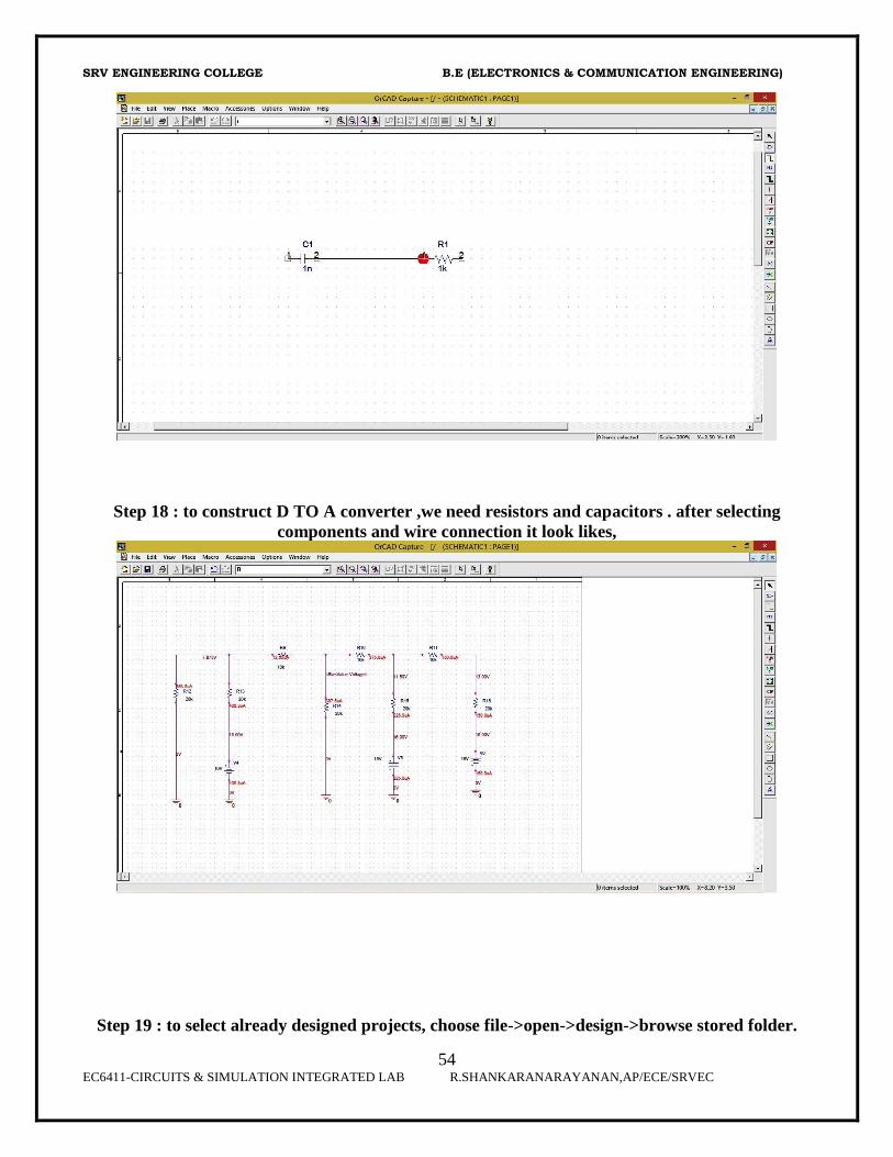
Step 18 : to construct D TO A converter ,we need resistors and capacitors . after selecting
components and wire connection it look likes,
Step 19 : to select already designed projects, choose file->open->design->browse stored folder.
SRV ENGINEERING COLLEGE B.E (ELECTRONICS & COMMUNICATION ENGINEERING)
EC6411-CIRCUITS & SIMULATION INTEGRATED LAB R.SHANKARANARAYANAN,AP/ECE/SRVEC
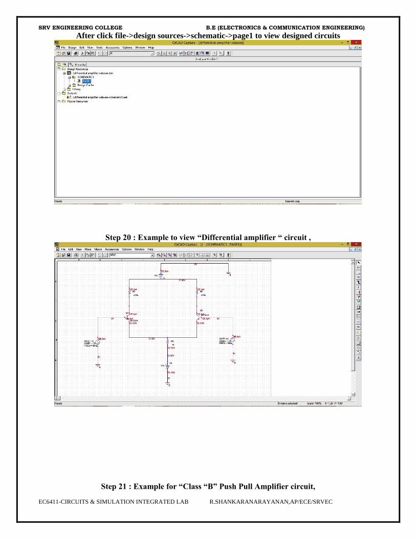
After click file->design sources->schematic->page1 to view designed circuits
Step 20 : Example to view “Differential amplifier “ circuit ,
Step 21 : Example for “Class “B” Push Pull Amplifier circuit,
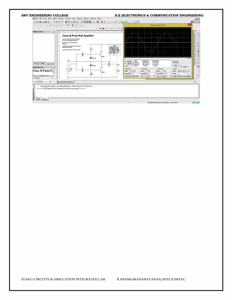
SRV ENGINEERING COLLEGE B.E (ELECTRONICS & COMMUNICATION ENGINEERING)
56 EC6411-CIRCUITS & SIMULATION INTEGRATED LAB R.SHANKARANARAYANAN,AP/ECE/SRVEC
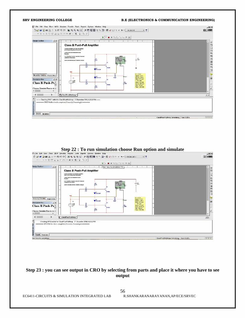
Step 22 : To run simulation choose Run option and simulate
Step 23 : you can see output in CRO by selecting from parts and place it where you have to see
output
SRV ENGINEERING COLLEGE B.E (ELECTRONICS & COMMUNICATION ENGINEERING)
EC6411-CIRCUITS & SIMULATION INTEGRATED LAB R.SHANKARANARAYANAN,AP/ECE/SRVEC

SRV ENGINEERING COLLEGE B.E (ELECTRONICS & COMMUNICATION ENGINEERING)
58 EC6411-CIRCUITS & SIMULATION INTEGRATED LAB R.SHANKARANARAYANAN,AP/ECE/SRVEC
CIRCUIT DIAGRAM:
R11kΩ
R21kΩ
R31kΩ
C1
1µF
C21µF
C31µF
L11mH
L21mH
U1
2N2219
Transformer
VCC
5V
Output
Q
Ex. no:
Date:
SPICE SIMULATION OF TUNED COLLECTOR OSCILLATOR
Aim:
To simulate a Tuned collector oscillator circuit and to plot the frequency response
characteristics.
Apparatus required :
i)Personal Computer
ii) SPICE (PSPICE 9.0 v& above or MULTISIM 10.0 v & above) Software.
Procedure:
i) Draw the circuit diagram after loading components from library.
ii) A DC source with 0 V is place as the dummy voltage source to obtain the current waveform.
iii) Wiring and proper net assignment has been made. The circuit is preprocessed. The VI
characteristics may be obtained by performing DC transfer function Analysis. Place the current
waveform marker at the positive terminal of the dummy voltage source (voltage =0 volts).
Iv) For placing waveform markers, select tools instruments set wave form conent current waveform
click on the required net and place the waveform marker.The sweep parameter (voltage) for input
source is set in the Analysis window.
V) The applied voltage is swept from an initial value to final value with the steps provided To get VI
characteristics, the currents corresponding to varying input voltages are noted.
vi) The VI graph is observed in the Waveform Viewer
Result :
Thus the Tuned collector oscillator is simulated successfully.
SRV ENGINEERING COLLEGE B.E (ELECTRONICS & COMMUNICATION ENGINEERING)
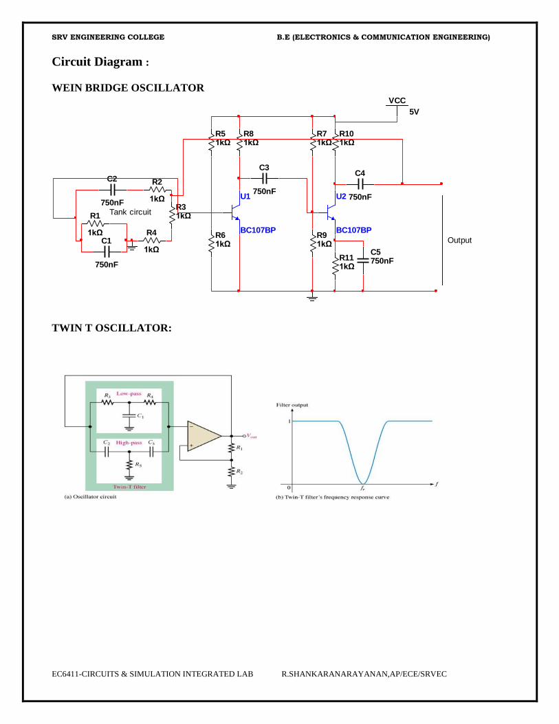
EC6411-CIRCUITS & SIMULATION INTEGRATED LAB R.SHANKARANARAYANAN,AP/ECE/SRVEC
Circuit Diagram :
WEIN BRIDGE OSCILLATOR
C1
750nF
C2
750nF
C3
750nF
C4
750nF
C5750nF
R1
1kΩ
R2
1kΩR31kΩ
R4
1kΩ
R51kΩ
R61kΩ
R71kΩ
R81kΩ
R91kΩ
R101kΩ
R111kΩ
U1
BC107BP
U2
BC107BP
VCC
5V
Tank circuit
Output
TWIN T OSCILLATOR:

SRV ENGINEERING COLLEGE B.E (ELECTRONICS & COMMUNICATION ENGINEERING)
60 EC6411-CIRCUITS & SIMULATION INTEGRATED LAB R.SHANKARANARAYANAN,AP/ECE/SRVEC
Ex. no:
Date:
SPICE SIMULATION OF WEIN BRIDGE AND TWIN T OSCILLATOR
Aim:
To simulate a Wein Bridge and Twin T oscillator circuit and to plot the frequency response
characteristics.
Apparatus required :
i)Personal Computer
ii) SPICE (PSPICE 9.0 v& above or MULTISIM 10.0 v & above) Software.
Procedure:
i) Draw the circuit diagram after loading components from library.
ii) A DC source with 0 V is place as the dummy voltage source to obtain the current waveform.
iii) Wiring and proper net assignment has been made. The circuit is preprocessed. The VI
characteristics may be obtained by performing DC transfer function Analysis. Place the current
waveform marker at the positive terminal of the dummy voltage source (voltage =0 volts).
Iv) For placing waveform markers, select tools instruments set wave form conent current waveform
click on the required net and place the waveform marker. The sweep parameter (voltage) for input
source is set in the Analysis window.
V) The applied voltage is swept from an initial value to final value with the steps provided To get VI
characteristics, the currents corresponding to varying input voltages are noted.
vi) The VI graph is observed in the Waveform Viewer
.
Result :
Thus the Wein Bridge and Twin T oscillator circuit is simulated successfully.
SRV ENGINEERING COLLEGE B.E (ELECTRONICS & COMMUNICATION ENGINEERING)
EC6411-CIRCUITS & SIMULATION INTEGRATED LAB R.SHANKARANARAYANAN,AP/ECE/SRVEC
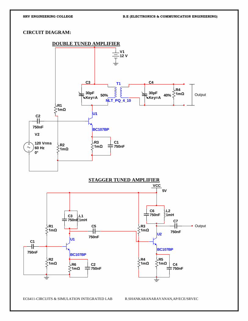
CIRCUIT DIAGRAM:
DOUBLE TUNED AMPLIFIER
V112 V
R11mΩ
R21mΩ
R31mΩ
C1750nF
C2
750nF
U1
BC107BP
C3
30pF
Key=A50%
C4
30pF
Key=A40%
T1
NLT_PQ_4_10
R41mΩ
V2
120 Vrms
60 Hz
0°
Output
STAGGER TUNED AMPLIFIER VCC
5V
U1
BC107BP
U2
BC107BP
R11mΩ
R21mΩ
R31mΩ
R41mΩ
R51mΩR6
1mΩ
L11mH
L21mH
C1
750nF
C2750nF
C3750nF
C4750nF
C5
750nF
C6750nF
C7
750nF
Output

SRV ENGINEERING COLLEGE B.E (ELECTRONICS & COMMUNICATION ENGINEERING)
62 EC6411-CIRCUITS & SIMULATION INTEGRATED LAB R.SHANKARANARAYANAN,AP/ECE/SRVEC
Ex. no:
Date:
SPICE SIMULATION OF DOUBLE AND STAGGER TUNED AMPLIFIERS
Aim:
To simulate a Double and Stagger tuned Amplifiers circuit and to plot the frequency response
characteristics.
Apparatus required :
i) Personal Computer
ii) SPICE (PSPICE 9.0 v& above or MULTISIM 10.0 v & above) Software.
Procedure:
i) Draw the circuit diagram after loading components from library.
ii) A DC source with 0 V is place as the dummy voltage source to obtain the current waveform.
iii) Wiring and proper net assignment has been made. The circuit is preprocessed. The VI
characteristics may be obtained by performing DC transfer function Analysis. Place the current
waveform marker at the positive terminal of the dummy voltage source (voltage =0 volts).
Iv) For placing waveform markers, select tools instruments set wave form conent current waveform
click on the required net and place the waveform marker.The sweep parameter (voltage) for input
source is set in the Analysis window.
V) The applied voltage is swept from an initial value to final value with the steps provided To get VI
characteristics, the currents corresponding to varying input voltages are noted.
vi) The VI graph is observed in the Waveform Viewer
Result :
Thus the Double and Stagger tuned Amplifier were simulated successfully.
SRV ENGINEERING COLLEGE B.E (ELECTRONICS & COMMUNICATION ENGINEERING)
EC6411-CIRCUITS & SIMULATION INTEGRATED LAB R.SHANKARANARAYANAN,AP/ECE/SRVEC
CIRCUIT DIAGRAM:
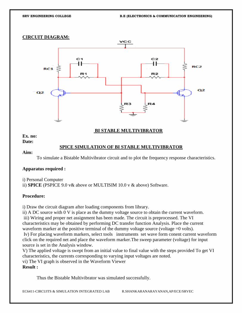
BI STABLE MULTIVIBRATOR
Ex. no:
Date:
SPICE SIMULATION OF BI STABLE MULTIVIBRATOR
Aim:
To simulate a Bistable Multivibrator circuit and to plot the frequency response characteristics.
Apparatus required :
i) Personal Computer
ii) SPICE (PSPICE 9.0 v& above or MULTISIM 10.0 v & above) Software.
Procedure:
i) Draw the circuit diagram after loading components from library.
ii) A DC source with 0 V is place as the dummy voltage source to obtain the current waveform.
iii) Wiring and proper net assignment has been made. The circuit is preprocessed. The VI
characteristics may be obtained by performing DC transfer function Analysis. Place the current
waveform marker at the positive terminal of the dummy voltage source (voltage =0 volts).
Iv) For placing waveform markers, select tools instruments set wave form conent current waveform
click on the required net and place the waveform marker.The sweep parameter (voltage) for input
source is set in the Analysis window.
V) The applied voltage is swept from an initial value to final value with the steps provided To get VI
characteristics, the currents corresponding to varying input voltages are noted.
vi) The VI graph is observed in the Waveform Viewer
Result :
Thus the Bistable Multivibrator was simulated successfully.
SRV ENGINEERING COLLEGE B.E (ELECTRONICS & COMMUNICATION ENGINEERING)
64 EC6411-CIRCUITS & SIMULATION INTEGRATED LAB R.SHANKARANARAYANAN,AP/ECE/SRVEC
CIRCUIT DIAGRAM:
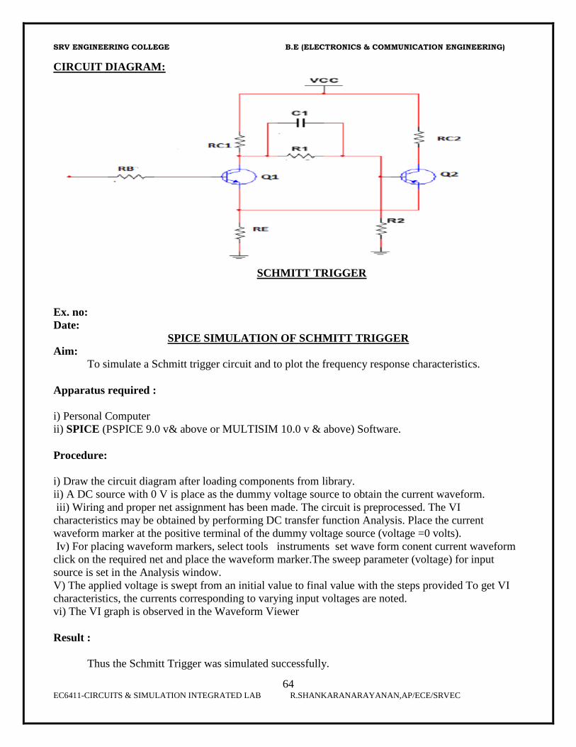
SCHMITT TRIGGER
Ex. no:
Date:
SPICE SIMULATION OF SCHMITT TRIGGER
Aim:
To simulate a Schmitt trigger circuit and to plot the frequency response characteristics.
Apparatus required :
i) Personal Computer
ii) SPICE (PSPICE 9.0 v& above or MULTISIM 10.0 v & above) Software.
Procedure:
i) Draw the circuit diagram after loading components from library.
ii) A DC source with 0 V is place as the dummy voltage source to obtain the current waveform.
iii) Wiring and proper net assignment has been made. The circuit is preprocessed. The VI
characteristics may be obtained by performing DC transfer function Analysis. Place the current
waveform marker at the positive terminal of the dummy voltage source (voltage =0 volts).
Iv) For placing waveform markers, select tools instruments set wave form conent current waveform
click on the required net and place the waveform marker.The sweep parameter (voltage) for input
source is set in the Analysis window.
V) The applied voltage is swept from an initial value to final value with the steps provided To get VI
characteristics, the currents corresponding to varying input voltages are noted.
vi) The VI graph is observed in the Waveform Viewer
Result :
Thus the Schmitt Trigger was simulated successfully.
SRV ENGINEERING COLLEGE B.E (ELECTRONICS & COMMUNICATION ENGINEERING)
EC6411-CIRCUITS & SIMULATION INTEGRATED LAB R.SHANKARANARAYANAN,AP/ECE/SRVEC
CIRCUIT DIAGRAM:
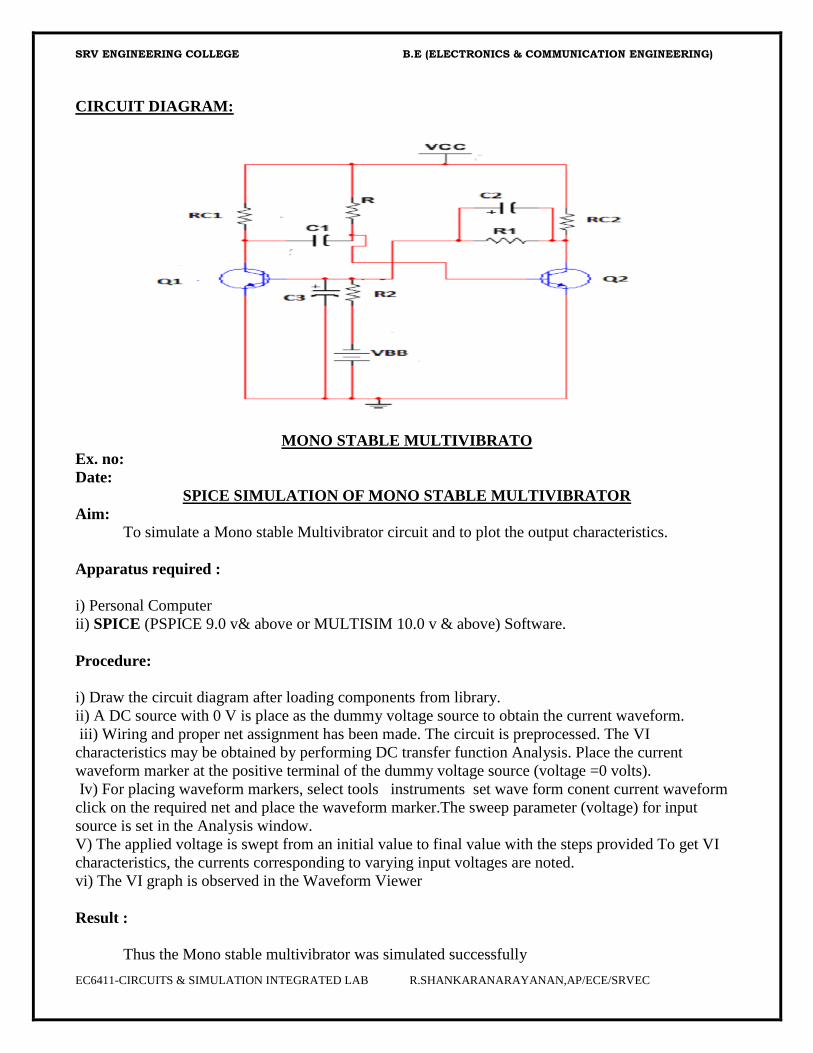
MONO STABLE MULTIVIBRATO
Ex. no:
Date:
SPICE SIMULATION OF MONO STABLE MULTIVIBRATOR
Aim:
To simulate a Mono stable Multivibrator circuit and to plot the output characteristics.
Apparatus required :
i) Personal Computer
ii) SPICE (PSPICE 9.0 v& above or MULTISIM 10.0 v & above) Software.
Procedure:
i) Draw the circuit diagram after loading components from library.
ii) A DC source with 0 V is place as the dummy voltage source to obtain the current waveform.
iii) Wiring and proper net assignment has been made. The circuit is preprocessed. The VI
characteristics may be obtained by performing DC transfer function Analysis. Place the current
waveform marker at the positive terminal of the dummy voltage source (voltage =0 volts).
Iv) For placing waveform markers, select tools instruments set wave form conent current waveform
click on the required net and place the waveform marker.The sweep parameter (voltage) for input
source is set in the Analysis window.
V) The applied voltage is swept from an initial value to final value with the steps provided To get VI
characteristics, the currents corresponding to varying input voltages are noted.
vi) The VI graph is observed in the Waveform Viewer
Result :
Thus the Mono stable multivibrator was simulated successfully
SRV ENGINEERING COLLEGE B.E (ELECTRONICS & COMMUNICATION ENGINEERING)
66 EC6411-CIRCUITS & SIMULATION INTEGRATED LAB R.SHANKARANARAYANAN,AP/ECE/SRVEC
CIRCUIT DIAGRAM:
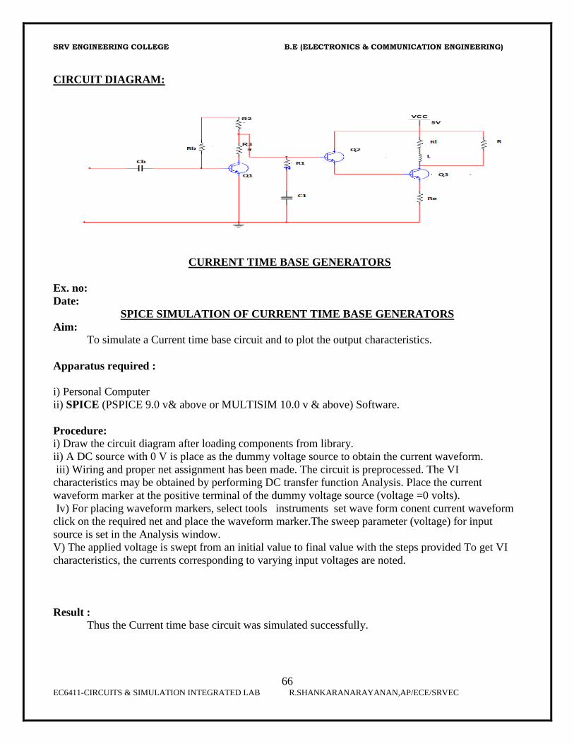
CURRENT TIME BASE GENERATORS
Ex. no:
Date:
SPICE SIMULATION OF CURRENT TIME BASE GENERATORS
Aim:
To simulate a Current time base circuit and to plot the output characteristics.
Apparatus required :
i) Personal Computer
ii) SPICE (PSPICE 9.0 v& above or MULTISIM 10.0 v & above) Software.
Procedure:
i) Draw the circuit diagram after loading components from library.
ii) A DC source with 0 V is place as the dummy voltage source to obtain the current waveform.
iii) Wiring and proper net assignment has been made. The circuit is preprocessed. The VI
characteristics may be obtained by performing DC transfer function Analysis. Place the current
waveform marker at the positive terminal of the dummy voltage source (voltage =0 volts).
Iv) For placing waveform markers, select tools instruments set wave form conent current waveform
click on the required net and place the waveform marker.The sweep parameter (voltage) for input
source is set in the Analysis window.
V) The applied voltage is swept from an initial value to final value with the steps provided To get VI
characteristics, the currents corresponding to varying input voltages are noted.
Result :
Thus the Current time base circuit was simulated successfully.