section 30. electrical specificationsww1.microchip.com/downloads/en/devicedoc/31030a.pdf · this...
TRANSCRIPT

M
Section 30. Electrical Specifications
Electrical
Sp
ecificatio
ns
30
HIGHLIGHTS
30.1 Introduction ..................................................................................................................30-230.2 Absolute Maximums.....................................................................................................30-330.3 Device Selection Table .................................................................................................30-430.4 Device Voltage Specifications ......................................................................................30-530.5 Device Current Specifications ......................................................................................30-630.6 Input Threshold Levels .................................................................................................30-930.7 I/O Current Specifications ..........................................................................................30-1030.8 Output Drive Levels....................................................................................................30-1130.9 I/O Capacitive Loading...............................................................................................30-1230.10 Data EEPROM / Flash ...............................................................................................30-1330.11 LCD............................................................................................................................30-1430.12 Comparators and Voltage Reference .........................................................................30-1530.13 Timing Parameter Symbology....................................................................................30-1630.14 Example External Clock Timing Waveforms and Requirements ................................30-1730.15 Example Power-up and Reset Timing Waveforms and Requirements.......................30-1930.16 Example Timer0 and Timer1 Timing Waveforms and Requirements .........................30-2030.17 Example CCP Timing Waveforms and Requirements................................................30-2130.18 Example Parallel Slave Port (PSP) Timing Waveforms and Requirements ...............30-2230.19 Example SSP and Master SSP SPI Mode Timing Waveforms and Requirements ....30-2330.20 Example SSP I2C Mode Timing Waveforms and Requirements................................30-2730.21 Example Master SSP I2C Mode Timing Waveforms and Requirements....................30-3030.22 Example USART/SCI Timing Waveforms and Requirements ....................................30-3230.23 Example 8-bit A/D Timing Waveforms and Requirements .........................................30-3430.24 Example 10-bit A/D Timing Waveforms and Requirements .......................................30-3630.25 Example Slope A/D Timing Waveforms and Requirements .......................................30-3830.26 Example LCD Timing Waveforms and Requirements ................................................30-4030.27 Related Application Notes..........................................................................................30-4130.28 Revision History .........................................................................................................30-42
1997 Microchip Technology Inc. DS31030A page 30-1
PICmicro MID-RANGE MCU FAMILY
30.1 Introduction
This section is intended to show you the electrical specifications that may be specified in a par-ticular device data sheet and what is meant by the specification. This section is NOT intended togive the values of these specifications. For the device specific values you must refer to thedevice’s data sheet. All values show in this section should be considered as Example Values.
In the description of the device and the functional modules (previous sections), there have beenreferences to electrical specification parameters. These references have been hyperlinked in theelectronic version to aid in the use of this manual.
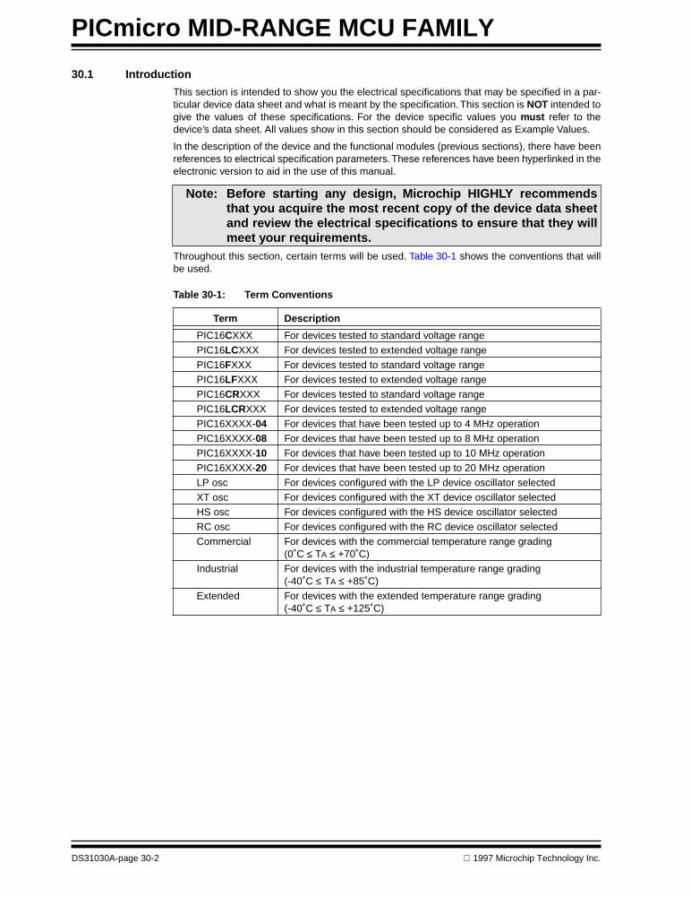
Throughout this section, certain terms will be used. Table 30-1 shows the conventions that willbe used.
Table 30-1: Term Conventions
Note: Before starting any design, Microchip HIGHLY recommendsthat you acquire the most recent copy of the device data sheetand review the electrical specifications to ensure that they willmeet your requirements.
Term Description
PIC16CXXX For devices tested to standard voltage rangePIC16LCXXX For devices tested to extended voltage rangePIC16FXXX For devices tested to standard voltage rangePIC16LFXXX For devices tested to extended voltage rangePIC16CRXXX For devices tested to standard voltage rangePIC16LCRXXX For devices tested to extended voltage rangePIC16XXXX-04 For devices that have been tested up to 4 MHz operationPIC16XXXX-08 For devices that have been tested up to 8 MHz operationPIC16XXXX-10 For devices that have been tested up to 10 MHz operationPIC16XXXX-20 For devices that have been tested up to 20 MHz operationLP osc For devices configured with the LP device oscillator selectedXT osc For devices configured with the XT device oscillator selectedHS osc For devices configured with the HS device oscillator selectedRC osc For devices configured with the RC device oscillator selectedCommercial For devices with the commercial temperature range grading
(0˚C ≤ TA ≤ +70˚C)Industrial For devices with the industrial temperature range grading
(-40˚C ≤ TA ≤ +85˚C)Extended For devices with the extended temperature range grading
(-40˚C ≤ TA ≤ +125˚C)
DS31030A-page 30-2 1997 Microchip Technology Inc.
Section 30. Electrical Specifications
Electrical
Sp
ecificatio
ns
30
30.2 Absolute Maximums
The Absolute Maximum Ratings specify the worst case conditions that can be applied to thedevice. These ratings are not meant as operational specifications, and stresses above the listedvalues may cause damage to the device. Specifications are not always stand-alone, that is, thespecification may have other requirements as well.
An example of this is the “maximum current sourced/sunk by any I/O pin”. The number of I/O pinsthat can be sinking/sourcing current, at any one time, is dependent upon the maximum currentsunk/source by the port(s) (combined) and the maximum current into the VDD pin or out of theVSS pin. In this example, the physical reason is the Power and Ground bus width to the I/O portsand internal logic. If these specifications are exceeded, then electromigration may occur on thesePower and Ground buses. Over time electromigration would cause these buses to open (be dis-connected from the pin), and therefore cause the logic attached to these buses to stop operating.So exceeding the absolute specifications may cause device reliability issues.
Input Clamp Current is defined as the current through the diode to VSS/VDD if pin voltage exceedsspecification.
Example Absolute Maximum Ratings†
Ambient temperature under bias........................................................................... . -55 to +125˚C
Storage temperature .......................................................................................... -65˚C to +150˚C
Voltage on any pin with respect to VSS (except VDD, MCLR, and RA4)..... -0.3V to (VDD + 0.3V)
Voltage on VDD with respect to VSS ....................................................................... -0.3 to +7.5V
Voltage on MCLR with respect to VSS (2) ...................................................................... 0 to +14V
Voltage on RA4 with respect to Vss .............................................................................. 0 to +14V
Total power dissipation (1) .................................................................................................... 1.0W
Maximum current out of VSS pin ...................................................................................... 300 mA
Maximum current into VDD pin ......................................................................................... 250 mA
Input clamp current, IIK (VI < 0 or VI > VDD).................................................................... ± 20 mA
Output clamp current, IOK (VO < 0 or VO > VDD) ............................................................. ± 20 mA
Maximum output current sunk by any I/O pin..................................................................... 25 mA
Maximum output current sourced by any I/O pin ............................................................... 25 mA
Maximum current sunk by PORTA, PORTB, and PORTE (combined)............................. 200 mA
Maximum current sourced by PORTA, PORTB, and PORTE (combined) ....................... 200 mA
Maximum current sunk by PORTC and PORTD (combined) ........................................... 200 mA
Maximum current sourced by PORTC and PORTD (combined)...................................... 200 mA
Maximum current sourced by PORTC and PORTD (combined)...................................... 200 mA
Maximum current sourced by PORTF and PORTG (combined) ...................................... 100 mA
Maximum current sourced by PORTF and PORTG (combined) ...................................... 100 mA
Note 1: Power dissipation is calculated as follows: Pdis = VDD x IDD - ∑ IOH + ∑ (VDD - VOH) x IOH + ∑(VOl x IOL)
Note 2: Voltage spikes below VSS at the MCLR pin, inducing currents greater than 80 mA,may cause latch-up. Thus, a series resistor of 50-100Ω should be used when apply-ing a “low” level to the MCLR pin rather than pulling this pin directly to VSS.
† NOTICE: Stresses above those listed under “Absolute Maximum Ratings” may cause perma-nent damage to the device. This is a stress rating only and functional operation of the device at those or any other conditions above those indicated in the operation listings of this specifica-tion is not implied. Exposure to maximum rating conditions for extended periods may affect device reliability.
1997 Microchip Technology Inc. DS31030A-page 30-3

PICmicro MID-RANGE MCU FAMILY
30.3 Device Selection Table
This table in the Device Data Sheet is intended to assist you in determining which oscillators aretested for which devices, and some of the specifications that are tested. Any oscillator may beselected at time of programming, but only the specified oscillator is tested by Microchip.
Since the RC and XT oscillators are only rated to 4 MHz, they are only tested on the -04 (4 MHz)devices.
PICmicros rated for 10 MHz or 20 MHz are only tested in HS mode. In Table 30-2 the IPD isgrayed out for the HS mode since there is not an IPD test point within the voltage range of the HSoscillator. The value shown is a typical value from characterization.
Battery applications usually require an extended voltage range. Devices marked LC have anextended voltage range and have the RC, XT, and LP oscillators tested.
Windowed devices are superset devices and have had the oscillators tested to all the specifica-tion ranges of the -04, -20, and LC devices. The temperature range that the device is tested toshould be considered commercial, though at a later time they may be tested to industrial orextended temperature levels.
Table 30-2: Example Cross Reference of Device Specifications for Oscillator Configurations and Frequencies of Operation (Commercial Devices)
OSC PIC16CXXX-04 PIC16CXXX-10 PIC16CXXX-20 PIC16LCXXX-04 Windowed Devices
RC
VDD: 4.0V to 6.0VIDD: 5 mA max. at 5.5VIPD: 16 µA max. at 4VFreq: 4 MHz max.
VDD: 4.5V to 5.5VIDD: 2.7 mA typ. at 5.5VIPD: 1.5 µA typ. at 4VFreq: 4 MHz max.
VDD: 4.5V to 5.5VIDD: 2.7 mA typ. at 5.5VIPD: 1.5 µA typ. at 4VFreq: 4 MHz max.
VDD: 2.5V to 6.0VIDD: 3.8 mA max. at 3.0VIPD: 5 µA max. at 3VFreq: 4 MHz max.
VDD: 2.5V to 6.0VIDD: 3.8 mA max. at 5.5VIPD: 16 µA max. at 4VFreq: 4 MHz max.
XT
VDD: 4.0V to 6.0VIDD: 5 mA max. at 5.5VIPD: 16 µA max. at 4VFreq: 4 MHz max.
VDD: 4.5V to 5.5VIDD: 2.7 mA typ. at 5.5VIPD: 1.5 µA typ. at 4VFreq: 4 MHz max.
VDD: 4.5V to 5.5VIDD: 2.7 mA typ. at 5.5VIPD: 1.5 µA typ. at 4VFreq: 4 MHz max.
VDD: 2.5V to 6.0VIDD: 3.8 mA max. at 3.0VIPD: 5 µA max. at 3VFreq: 4 MHz max.
VDD: 2.5V to 6.0VIDD: 3.8 mA max. at 5.5VIPD: 16 µA max. at 4VFreq: 4 MHz max.
HS
VDD: 4.5V to 5.5V VDD: 4.5V to 5.5V VDD: 4.5V to 5.5V
Not recommended for use in HS mode
VDD: 4.5V to 5.5V
IDD: 13.5 mA typ. at 5.5V IDD: 10 mA max. at 5.5V IDD: 20 mA max. at 5.5V IDD: 20 mA max. at 5.5V
IPD: 1.5 µA typ. at 4.5V IPD: 1.5 µA typ. at 4.5V IPD: 1.5 µA typ. at 4.5V IPD: 1.5 µA typ. at 4.5V
Freq: 4 MHz max. Freq: 10 MHz max. Freq: 20 MHz max. Freq: 20 MHz max.
LP
VDD: 4.0V to 6.0VIDD: 52.5 µA typ. at
32 kHz, 4.0VIPD: 0.9 µA typ. at 4.0VFreq: 200 kHz max.
Not recommended for use in LP mode
Not recommended for use in LP mode
VDD: 2.5V to 6.0VIDD: 48 µA max. at
32 kHz, 3.0VIPD: 5.0 µA max. at 3.0VFreq: 200 kHz max.
VDD: 2.5V to 6.0VIDD: 48 µA max. at
32 kHz, 3.0VIPD: 5.0 µA max. at 3.0VFreq: 200 kHz max.
The shaded sections indicate oscillator selections which are tested for functionality, but not for MIN/MAX specifications. It is recommended that the user select the device type that ensures the specifications required.
Note: Devices that are marked with Engineering Sample (ENG SMP) are tested to the cur-rent engineering test program at time of the device testing. There is no implied war-ranty that these devices have been tested to any or all specifications in the DeviceData Sheet.
DS31030A-page 30-4 1997 Microchip Technology Inc.
Section 30. Electrical SpecificationsE
lectrical S
pecifi
cation
s
30
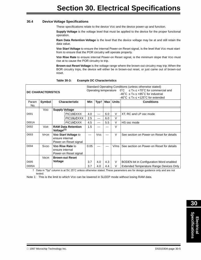
30.4 Device Voltage Specifications
These specifications relate to the device VDD and the device power-up and function.
Supply Voltage is the voltage level that must be applied to the device for the proper functionaloperation.
Ram Data Retention Voltage is the level that the device voltage may be at and still retain thedata value.
VDD Start Voltage to ensure the internal Power-on Reset signal, is the level that VDD must start from to ensure that the POR circuitry will operate properly.
VDD Rise Rate to ensure internal Power-on Reset signal, is the minimum slope that VDD mustrise at to cause the POR circuitry to trip.
Brown-out Reset Voltage is the voltage range where the brown-out circuitry may trip. When theBOR circuitry trips, the device will either be in brown-out reset, or just came out of brown-outreset.
Table 30-3: Example DC Characteristics
DC CHARACTERISTICS
Standard Operating Conditions (unless otherwise stated)Operating temperature 0˚C ≤ TA ≤ +70˚C for commercial and
-40˚C ≤ TA ≤ +85˚C for industrial -40˚C ≤ TA ≤ +125˚C for extended
Param No.
Symbol Characteristic Min Typ† Max Units Conditions
VDD Supply VoltageD001 PIC16CXXX 4.0 — 6.0 V XT, RC and LP osc mode
PIC16LCXXX 2.5 — 6.0 VD001A PIC16CXXX 4.5 — 5.5 V HS osc modeD002 VDR RAM Data Retention
Voltage(1)1.5 — — V
D003 VPOR VDD Start Voltage to ensure internal Power-on Reset signal
— VSS — V See section on Power-on Reset for details
D004 SVDD VDD Rise Rate to ensure internal Power-on Reset signal
0.05 — — V/ms See section on Power-on Reset for details
VBOR Brown-out Reset VoltageD005 3.7 4.0 4.3 V BODEN bit in Configuration Word enabled
D005A 3.7 4.0 4.4 V Extended Temperature Range Devices Only† Data in “Typ” column is at 5V, 25˚C unless otherwise stated. These parameters are for design guidance only and are not
tested.Note 1: This is the limit to which VDD can be lowered in SLEEP mode without losing RAM data.
1997 Microchip Technology Inc. DS31030A-page 30-5

PICmicro MID-RANGE MCU FAMILY
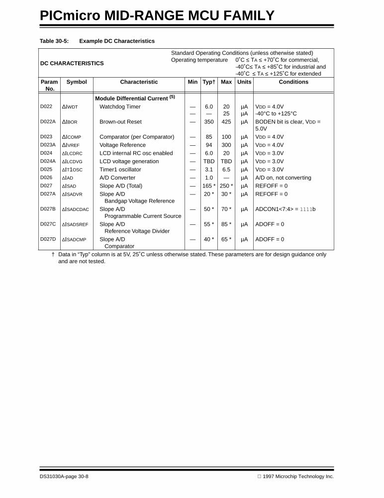
30.5 Device Current Specifications
IDD is the current (I) that the device consumes when the device is in operating mode. This test istaken with all I/O as inputs, either pulled high or low. That is, there are no floating inputs, nor areany pins driving an output (with a load).
IPD is the current (I) that the device consumes when the device is in sleep mode (power-down),referred to as power-down current. These tests are taken with all I/O as inputs, either pulled highor low. That is, there are no floating inputs, nor are any pins driving an output (with a load), weakpull-ups are disabled.
A device may have certain features and modules that can operate while the device is in sleepmode. Some on these modules are:
• Watchdog Timer (WDT)• Brown-out Reset (BOR) circuitry• Timer1• Analog to Digital converter• LCD module• Comparators• Voltage Reference
When all features are disabled, the device will consume the lowest possible current (the leakagecurrent). If any of these features are operating while the device is in sleep, a higher current willoccur. The difference between the lowest power mode (everything off) at only that one featureenabled (such as the WDT) is what we call the Module Differential Current. If more then onefeature is enabled then the expected current can easily be calculated as: the base current (every-thing disabled and in sleep mode) plus all Module Differential Currents (delta currents).Example 30-1 shows an example of calculating the typical currents for a device at 5V, with theWDT and Timer1 oscillator enabled.
Example 30-1: IPD Calculations with WDT and Timer1 Oscillator Enabled (@ 5V)
Base Current 14 nA ; Device leakage currentWDT Delta Current 14 µA ; 14 µA - 14 nA = 14 µA Timer1 Delta Current 22 µA ; 22 µA - 14 nA = 22 µA Total Sleep Current 36 µA ;
DS31030A-page 30-6 1997 Microchip Technology Inc.

Section 30. Electrical SpecificationsE
lectrical S
pecifi
cation
s
30
Table 30-4: Example DC Characteristics
DC CHARACTERISTICS
Standard Operating Conditions (unless otherwise stated) Operating temperature 0˚C ≤ TA ≤ +70˚C for commercial and
-40˚C ≤ TA ≤ +85˚C for industrial -40˚C ≤ TA ≤ +125˚C for extended
Param No.
Symbol Characteristic Min Typ† Max Units Conditions
D010
D010A
D010C
D013
IDD Supply Current(2,4,5)
——
—
—
—
2.72.0
22.5
7.7
13.5
53.8
48
5
30
mAmA
µA
mA
mA
XT, RC osc configuration (PIC16CXXX-04)FOSC = 4 MHz, VDD = 5.5V FOSC = 4 MHz, VDD = 3.0V
LP osc configurationFOSC = 32 kHz, VDD = 3.0V, WDT disabled
INTRC osc configuration, Fosc = 4 MHz, VDD = 5.5V
HS osc configuration (PIC16CXXX-20)Fosc = 20 MHz, VDD = 5.5V
D020
D021
D021AD021B
IPD Power-down Current(3,5)
———
——
——
10.57.51.5
0.91.5
0.91.5
423021
13.524
18—
µAµAµA
µAµA
µAµA
VDD = 4.0V, WDT enabled, -40°C to +85°CVDD = 3.0V, WDT enabled, -40°C to +85°CVDD = 4.0V, WDT disabled, -0°C to +70°C
VDD = 3.0V, WDT disabled, 0°C to +70°CVDD = 4.0V, WDT disabled, -40°C to +85°C
VDD = 3.0V, WDT disabled, -40°C to +85°CVDD = 4.0V, WDT disabled, -40°C to +125°C
* These parameters are characterized but not tested.† Data in “Typ” column is at 5V, 25˚C unless otherwise stated. These parameters are for design guidance only
and are not tested.Note 1: Not Applicable.
2: The supply current is mainly a function of the operating voltage and frequency. Other factors such as I/O pin loading and switching rate, oscillator type, internal code execution pattern, and temperature also have an impact on the current consumption.The test conditions for all IDD measurements in active operation mode are: OSC1 = external square wave, from rail to rail; all I/O pins tristated, pulled to VDD MCLR = VDD; WDT enabled/disabled as specified.
3: The power-down current in SLEEP mode does not depend on the oscillator type. Power-down current is mea-sured with the part in SLEEP mode, with all I/O pins in hi-impedance state and tied to VDD and VSS.
4: For RC osc configuration, current through Rext is not included. The current through the resistor can be esti-mated by the formula Ir = VDD/2Rext (mA) with Rext in kOhm.
5: Timer1 oscillator (when enabled) adds approximately 20 µA to the specification. This value is from character-ization and is for design guidance only. This is not tested.
1997 Microchip Technology Inc. DS31030A-page 30-7
PICmicro MID-RANGE MCU FAMILY
Table 30-5: Example DC Characteristics
DC CHARACTERISTICS
Standard Operating Conditions (unless otherwise stated) Operating temperature 0˚C ≤ TA ≤ +70˚C for commercial,
-40˚C≤ TA ≤ +85˚C for industrial and -40˚C ≤ TA ≤ +125˚C for extended
Param No.
Symbol Characteristic Min Typ† Max Units Conditions
Module Differential Current (5)
D022 ∆IWDT Watchdog Timer ——
6.0—
2025
µAµA
VDD = 4.0V-40°C to +125°C
D022A ∆IBOR Brown-out Reset — 350 425 µA BODEN bit is clear, VDD = 5.0V
D023 ∆ICOMP Comparator (per Comparator) — 85 100 µA VDD = 4.0VD023A ∆IVREF Voltage Reference — 94 300 µA VDD = 4.0VD024 ∆ILCDRC LCD internal RC osc enabled — 6.0 20 µA VDD = 3.0VD024A ∆ILCDVG LCD voltage generation — TBD TBD µA VDD = 3.0VD025 ∆IT1OSC Timer1 oscillator — 3.1 6.5 µA VDD = 3.0VD026 ∆IAD A/D Converter — 1.0 — µA A/D on, not convertingD027 ∆ISAD Slope A/D (Total) — 165 * 250 * µA REFOFF = 0D027A ∆ISADVR Slope A/D
Bandgap Voltage Reference— 20 * 30 * µA REFOFF = 0
D027B ∆ISADCDAC Slope A/D Programmable Current Source
— 50 * 70 * µA ADCON1<7:4> = 1111b
D027C ∆ISADSREF Slope A/D Reference Voltage Divider
— 55 * 85 * µA ADOFF = 0
D027D ∆ISADCMP Slope A/D Comparator
— 40 * 65 * µA ADOFF = 0
† Data in “Typ” column is at 5V, 25˚C unless otherwise stated. These parameters are for design guidance only and are not tested.
DS31030A-page 30-8 1997 Microchip Technology Inc.

Section 30. Electrical SpecificationsE
lectrical S
pecifi
cation
s
30
30.6 Input Threshold Levels
The Input Low Voltage (VIL) is the voltage level that will be read as a logic ’0’. An input may notread a ’0’ at a voltage level above this. All designs should be to the specification since device todevice (and to a much lesser extent pin to pin) variations will cause this level to vary.
The Input High Voltage (VIH) is the voltage level that will be read as a logic ’1’. An input mayread a ’1’ at a voltage level below this. All designs should be to the specification since device todevice (and to a much lesser extent pin to pin) variations will cause this level to vary.
The I/O pins with TTL levels are shown with two specifications. One is the industry standard TTLspecification, which is specified for the voltage range of 4.5V to 5.5V. The other is a specificationthat operates over the entire voltage range of the device. The better of these two specificationsmay be used in the design.
Table 30-6: Example DC Characteristics
DC CHARACTERISTICS
Standard Operating Conditions (unless otherwise stated)Operating temperature 0˚C ≤ TA ≤ +70˚C for commercial,
-40˚C ≤ TA ≤ +85˚C for industrial and -40˚C ≤ TA ≤ +125˚C for extended
Operating voltage VDD range as described in DC spec Table 30-3.Param
No.Symbol Characteristic Min Typ† Max Units Conditions
VIL Input Low VoltageI/O ports:
D030 with TTL buffer VSS — 0.15VDD V For entire VDD range (4) D030A — — 0.8 V 4.5V ≤ VDD ≤ 5.5V (4)
D031 with Schmitt Trigger buffer VSS — 0.2VDD V For entire VDD range
D032 MCLR, OSC1 (RC mode) VSS — 0.2VDD VD033 OSC1
(XT, HS and LP modes)(1)VSS — 0.3VDD V
VIH Input High VoltageI/O ports:
D040 with TTL buffer 0.25VDD + 0.8V
— VDD V For entire VDD range (4)
D040A 2.0 — VDD V 4.5V ≤ VDD ≤ 5.5V (4)
D041 with Schmitt Trigger buffer 0.8VDD — VDD V For entire VDD range
D042 MCLR 0.8VDD — VDD VD042A OSC1
(XT, HS and LP modes)(1)0.7VDD — VDD V
D043 OSC1 (RC mode) 0.9VDD — VDD VD050 VHYS Hysteresis of Schmitt Trigger
InputsTBD — — V
† Data in “Typ” column is at 5V, 25°C unless otherwise stated. These parameters are for design guidance only and are not tested.
Note 1: In RC oscillator configuration, the OSC1/CLKIN pin is a Schmitt Trigger input. It is not recommended that the PICmicro be driven with an external clock while in RC mode.
2: Not Applicable.3: Not Applicable.4: The better of the two specifications may be used. For VIL this would be the higher voltage and for VIH this
would be the lower voltage.
1997 Microchip Technology Inc. DS31030A-page 30-9

PICmicro MID-RANGE MCU FAMILY
30.7 I/O Current Specifications
The PORT/GIO Weak Pull-up Current is the additional current that the device will draw whenthe weak pull-ups are enabled.
Leakage Currents are the currents that the device consumes, since the devices are manufac-tured in the real world and do not adhere to their ideal characteristics. Ideally there should be nocurrent on an input, but due to the real world there is always some parasitic path that consumesnegligible current.
Table 30-7: Example DC Characteristics
DC CHARACTERISTICS
Standard Operating Conditions (unless otherwise stated)Operating temperature 0˚C ≤ TA ≤ +70˚C for commercial,
-40˚C ≤ TA ≤ +85˚C for industrial and -40˚C ≤ TA ≤ +125˚C for extended
Operating voltage VDD range as described in DC spec Table 30-3.Param
No.Symbol Characteristic Min Typ† Max Units Conditions
IIL Input Leakage Current(2,3) D060 I/O ports — — ±1 µA Vss ≤ VPIN ≤ VDD,
Pin at hi-impedanceD060A CDAC — — ±1 µA Vss ≤ VPIN ≤ VDD,
Pin at hi-impedanceD061 MCLR — — ±5 µA Vss ≤ VPIN ≤ VDD
D063 — — ±5 µA Vss ≤ VPIN ≤ VDD, XT, HS and LP osc modes
IPU Weak Pull-up CurrentD070 IPURB PORTB weak pull-up current 50 250 400 µA VDD = 5V, VPIN = VSS
D070A IPUGIO GIO weak pull-up current 50 250 400 µA VDD = 5V, VPIN = VSS
Programmable Current Source (Slope A/D devices)
CDAC pin = 0V
D160 Output Current 18.75 33.75 48.75 µA ADCON1<7:4> = 1111b (full-scale)
D160A 1.25 2.25 3.25 µA ADCON1<7:4> = 0001b (1 LSB)D160B -0.5 0 0.5 µA ADCON1<7:4> = 0000b
(zero-scale)† Data in “Typ” column is at 5V, 25°C unless otherwise stated. These parameters are for design guidance only
and are not tested.Note 1: In RC oscillator configuration, the OSC1/CLKIN pin is a Schmitt Trigger input. It is not recommended that the
PICmicro be driven with an external clock while in RC mode.2: The leakage current on the MCLR pin is strongly dependent on the applied voltage level. The specified lev-
els represent normal operating conditions. Higher leakage current may be measured at different input volt-ages.
3: Negative current is defined as current sourced by the pin.
DS31030A-page 30-10 1997 Microchip Technology Inc.
Section 30. Electrical SpecificationsE
lectrical S
pecifi
cation
s
30
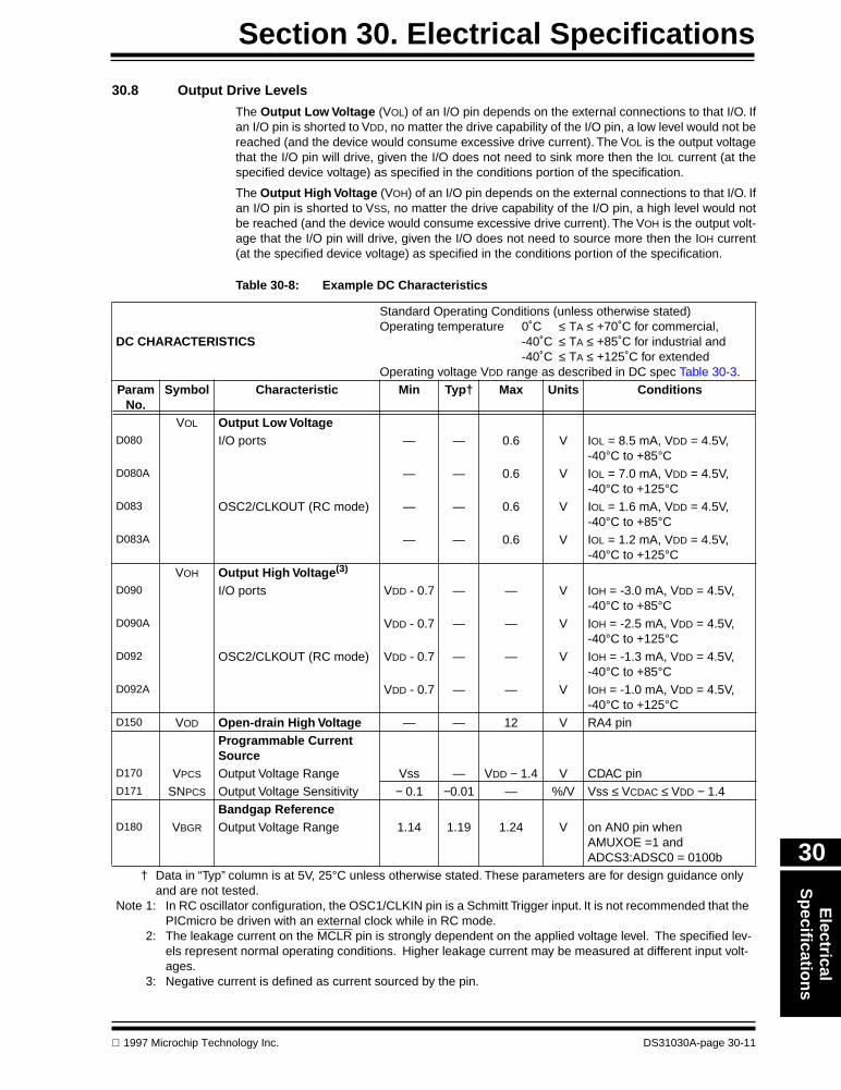
30.8 Output Drive Levels
The Output Low Voltage (VOL) of an I/O pin depends on the external connections to that I/O. Ifan I/O pin is shorted to VDD, no matter the drive capability of the I/O pin, a low level would not bereached (and the device would consume excessive drive current). The VOL is the output voltagethat the I/O pin will drive, given the I/O does not need to sink more then the IOL current (at thespecified device voltage) as specified in the conditions portion of the specification.
The Output High Voltage (VOH) of an I/O pin depends on the external connections to that I/O. Ifan I/O pin is shorted to VSS, no matter the drive capability of the I/O pin, a high level would notbe reached (and the device would consume excessive drive current). The VOH is the output volt-age that the I/O pin will drive, given the I/O does not need to source more then the IOH current(at the specified device voltage) as specified in the conditions portion of the specification.
Table 30-8: Example DC Characteristics
DC CHARACTERISTICS
Standard Operating Conditions (unless otherwise stated)Operating temperature 0˚C ≤ TA ≤ +70˚C for commercial,
-40˚C ≤ TA ≤ +85˚C for industrial and -40˚C ≤ TA ≤ +125˚C for extended
Operating voltage VDD range as described in DC spec Table 30-3.Param
No.Symbol Characteristic Min Typ† Max Units Conditions
VOL Output Low VoltageD080 I/O ports — — 0.6 V IOL = 8.5 mA, VDD = 4.5V,
-40°C to +85°CD080A — — 0.6 V IOL = 7.0 mA, VDD = 4.5V,
-40°C to +125°CD083 OSC2/CLKOUT (RC mode) — — 0.6 V IOL = 1.6 mA, VDD = 4.5V,
-40°C to +85°CD083A — — 0.6 V IOL = 1.2 mA, VDD = 4.5V,
-40°C to +125°CVOH Output High Voltage(3)
D090 I/O ports VDD - 0.7 — — V IOH = -3.0 mA, VDD = 4.5V, -40°C to +85°C
D090A VDD - 0.7 — — V IOH = -2.5 mA, VDD = 4.5V, -40°C to +125°C
D092 OSC2/CLKOUT (RC mode) VDD - 0.7 — — V IOH = -1.3 mA, VDD = 4.5V, -40°C to +85°C
D092A VDD - 0.7 — — V IOH = -1.0 mA, VDD = 4.5V, -40°C to +125°C
D150 VOD Open-drain High Voltage — — 12 V RA4 pinProgrammable Current Source
D170 VPCS Output Voltage Range Vss — VDD − 1.4 V CDAC pinD171 SNPCS Output Voltage Sensitivity − 0.1 −0.01 — %/V Vss ≤ VCDAC ≤ VDD − 1.4
Bandgap Reference D180 VBGR Output Voltage Range 1.14 1.19 1.24 V on AN0 pin when
AMUXOE =1 and ADCS3:ADSC0 = 0100b
† Data in “Typ” column is at 5V, 25°C unless otherwise stated. These parameters are for design guidance only and are not tested.
Note 1: In RC oscillator configuration, the OSC1/CLKIN pin is a Schmitt Trigger input. It is not recommended that the PICmicro be driven with an external clock while in RC mode.
2: The leakage current on the MCLR pin is strongly dependent on the applied voltage level. The specified lev-els represent normal operating conditions. Higher leakage current may be measured at different input volt-ages.
3: Negative current is defined as current sourced by the pin.
1997 Microchip Technology Inc. DS31030A-page 30-11

PICmicro MID-RANGE MCU FAMILY
30.9 I/O Capacitive Loading
These specifications indicate the conditions that the I/O pins have on them from the device tester.These loadings effect the specifications for the timing specifications. If the loading in you appli-cation are different, then you will need to determine how this will effect the characteristic of thedevice in your system. Capacitances less then these specifications should not have effects on asystem.
Table 30-9: Example DC Characteristics
DC CHARACTERISTICS
Standard Operating Conditions (unless otherwise stated)Operating temperature 0˚C ≤ TA ≤ +70˚C for commercial
-40˚C ≤ TA ≤ +85˚C for industrial and -40˚C ≤ TA ≤ +125˚C for extended
Operating voltage VDD range as described in DC spec Table 30-3.Param
No.Symbol Characteristic Min Typ† Max Units Conditions
Capacitive Loading Specson Output Pins
D100 COSC2 OSC2 pin — — 15 pF In XT, HS and LP modes when external clock is used to drive OSC1.
D101 CIO All I/O pins and OSC2 (in RC mode)
— — 50 pF To meet the Timing Specifications of the Device
D102 CB SCL, SDA — — 400 pF In I2C mode† Data in “Typ” column is at 5V, 25°C unless otherwise stated. These parameters are for design guidance only
and are not tested.Note 1: In RC oscillator configuration, the OSC1/CLKIN pin is a Schmitt Trigger input. It is not recommended that
the PICmicro be driven with external clock in RC mode.2: The leakage current on the MCLR pin is strongly dependent on the applied voltage level. The specified lev-
els represent normal operating conditions. Higher leakage current may be measured at different input volt-ages.
3: Negative current is defined as current sourced by the pin.
DS31030A-page 30-12 1997 Microchip Technology Inc.

Section 30. Electrical SpecificationsE
lectrical S
pecifi
cation
s
30
30.10 Data EEPROM / Flash
Table 30-10: Example Data EEPROM / Flash Characteristics
DC CHARACTERISTICS
Standard Operating Conditions (unless otherwise stated)Operating temperature 0˚C ≤ TA ≤ +70˚C for commercial,
-40˚C ≤ TA ≤ +85˚C for industrial and -40˚C ≤ TA ≤ +125˚C for extended
Operating voltage VDD range as described in DC spec Table 30-3.
ParamNo.
Symbol Characteristic Min Typ† Max Units Conditions
Data EEPROM MemoryD120 ED Endurance 1M 10M — E/W 25°C at 5VD121 VDRW VDD for read/write VMIN — 6.0 V VMIN = Minimum operating
voltageD122 TDEW Erase/Write cycle time — — 10 ms
Program Flash MemoryD130 EP Endurance 100 1000 — E/WD131 VPR VDD for read VMIN — 6.0 V VMIN = Minimum operating
voltageD132 VPEW VDD for erase/write 4.5 — 5.5 VD133 TPEW Erase/Write cycle time — — 10 ms
† Data in “Typ” column is at 5.0V, 25°C unless otherwise stated. These parameters are for design guidance only and are not tested.
1997 Microchip Technology Inc. DS31030A-page 30-13

PICmicro MID-RANGE MCU FAMILY
30.11 LCD
Table 30-11: Example LCD Module Electrical Characteristics
Table 30-12: Example VLCD Charge Pump Electrical Characteristics
DC CHARACTERISTICS
Standard Operating Conditions (unless otherwise stated)Operating temperature 0˚C ≤ TA ≤ +70˚C for commercial,
-40˚C ≤ TA ≤ +85˚C for industrial and -40˚C ≤ TA ≤ +125˚C for extended
Operating voltage VDD range as described in DC spec Table 30-3.
ParamNo.
Symbol Characteristic Min Typ† Max Units Conditions
D200 VLCD3 LCD Voltage on pin VLCD3
VDD - 0.3 — Vss + 7.0 V
D201 VLCD2 LCD Voltage on pin VLCD2
— — VLCD3 V
D202 VLCD1 LCD Voltage on pin VLCD1
— — VDD V
D210 RCOM Com Output Source Impedance
— — 1k Ω COM outputs
D211 RSEG Seg Output Source Impedance
— — 10k Ω SEG outputs
D220 VOH Output High Voltage Max (VLCDN) - 0.1
— Max (VLCDN) V COM outputs IOH = 25 µASEG outputs IOH = 3 µA
D221 VOL Output Low Voltage Min (VLCDN) — Min (VLCDN) + 0.1
V COM outputs IOL = 25 µASEG outputs IOL = 3 µA
† Data in “Typ” column is at 5V, 25°C unless otherwise stated. These parameters are for design guidance only and are not tested.
Note 1: 0 ohm source impedance at VLCD.
DC CHARACTERISTICS
Standard Operating Conditions (unless otherwise stated)Operating temperature 0˚C ≤ TA ≤ +70˚C for commercial,
-40˚C ≤ TA ≤ +85˚C for industrial and -40˚C ≤ TA ≤ +125˚C for extended
Operating voltage VDD range as described in DC spec Table 30-3.
ParamNo.
Symbol Characteristic Min Typ Max Units Conditions
D250 IVADJ VLCDADJ Regulated Current Output — 10 — µA
D251 Ivr VLCDADJ Current Consumption — — 20 µA
D252 ∆ IVADJ
∆ VDD
VLCDADJ Current VDD Rejection — — 0.1/1 µA/V
D253 ∆ IVADJ
∆ TVLCDADJ Current Variation With Tem-perature
— — 0.1/70 µA/˚C
D260(1) RVADJ VLCDADJ External Resistor 100 — 230 kΩ
D265 VVADJ VLCDADJ Voltage Limits 1.0 — 2.3 V
D271(1) CECPC External Charge Pump Capacitance — 0.5 — µF
Note 1: For design guidance only.
DS31030A-page 30-14 1997 Microchip Technology Inc.

Section 30. Electrical SpecificationsE
lectrical S
pecifi
cation
s
30
30.12 Comparators and Voltage Reference
Table 30-13: Example Comparator Characteristics
Table 30-14: Example Voltage Reference Characteristics
DC CHARACTERISTICS
Standard Operating Conditions (unless otherwise stated)Operating temperature 0˚C ≤ TA ≤ +70˚C for commercial,
-40˚C ≤ TA ≤ +85˚C for industrial and -40˚C ≤ TA ≤ +125˚C for extended
Operating voltage VDD range as described in DC spec Table 30-3.
ParamNo.
Symbol Characteristics Min Typ Max Units Comments
D300 VIOFF Input offset voltage — ± 5.0 ± 10 mV
D301 VICM Input common mode voltage 0 — VDD - 1.5 V
D302 CMRR Common Mode Rejection Ratio 35 70 — db
300 TRESP Response Time(1) PIC16CXXX — 150 400 ns
300A PIC16LCXXX — 210 600 ns
301 TMC2OV Comparator Mode Change to Output Valid
— — 10 µs
Note 1: Response time measured with one comparator input at (VDD - 1.5)/2 while the other input transitions from VSS to VDD.
DC CHARACTERISTICS
Standard Operating Conditions (unless otherwise stated)Operating temperature 0˚C ≤ TA ≤ +70˚C for commercial,
-40˚C ≤ TA ≤ +85˚C for industrial and -40˚C ≤ TA ≤ +125˚C for extended
Operating voltage VDD range as described in DC spec Table 30-3.
ParamNo.
Symbol Characteristics Min Typ Max Units Comments
D310 VRES Resolution VDD/32 — VDD/24 V
D311 VRAA Absolute Accuracy ——
——
1/41/2
LSbLSb
Low Range (VRR = 1)High Range (VRR = 0)
D312 VRUR Unit Resistor Value (R) — 2k — Ω310 TSET Settling Time(1) — — 10 µs
Note 1: Settling time measured while VRR = 1 and VR3:VR0 transitions from 0000 to 1111.
1997 Microchip Technology Inc. DS31030A-page 30-15

PICmicro MID-RANGE MCU FAMILY
30.13 Timing Parameter Symbology
The timing parameter symbols have been created with one of the following formats:
Figure 30-1: Example Load Conditions
1. TppS2ppS 3. TCC:ST (I2C specifications only)2. TppS 4. Ts (I2C specifications only)TF Frequency T TimeLowercase letters (pp) and their meanings:ppcc CCP1 osc OSC1ck CLKOUT rd RDcs CS rw RD or WRdi SDI sc SCKdo SDO ss SSdt Data in t0 T0CKIio I/O port t1 T1CKImc MCLR wr WRUppercase letters and their meanings:SF Fall P PeriodH High R RiseI Invalid (Hi-impedance) V ValidL Low Z Hi-impedanceI2C onlyAA output access High HighBUF Bus free Low LowTCC:ST (I2C specifications only)CCHD Hold SU SetupSTDAT DATA input hold STO STOP conditionSTA START condition
VDD/2
CL
RL
Pin Pin
VSS VSS
CL
RL = 464Ω
CL = 50 pF for all pins except OSC2
15 pF for OSC2 output
Load condition 1 Load condition 2
DS31030A-page 30-16 1997 Microchip Technology Inc.

Section 30. Electrical SpecificationsE
lectrical S
pecifi
cation
s
30
30.14 Example External Clock Timing Waveforms and Requirements
Figure 30-2: Example External Clock Timing Waveforms
Table 30-15: Example External Clock Timing Requirements
Param. No.
Symbol Characteristic Min Typ† Max Units Conditions
1A Fosc External CLKIN Frequency(1)
DC — 4 MHz XT and RC osc PIC16CXXX-04 PIC16LCXXX-04
DC — 10 MHz HS osc PIC16CXXX-10DC — 20 MHz PIC16CXXX-20DC — 200 kHz LP osc PIC16LCXXX-04
Oscillator Frequency(1) DC — 4 MHz RC osc PIC16CXXX-04 PIC16LCXXX-04
0.1 — 4 MHz XT osc PIC16CXXX-04 PIC16LCXXX-04
4 — 10 MHz HS osc PIC16CXXX-104 — 20 MHz PIC16CXXX-205 — 200 kHz LP osc mode PIC16LCXXX-04
1 Tosc External CLKIN Period(1) 250 — — ns XT and RC osc PIC16CXXX-04 PIC16LCXXX-04
100 — — ns HS osc PIC16CXXX-1050 — — ns PIC16CXXX-205 — — µs LP osc PIC16LCXXX-04
Oscillator Period(1) 250 — — ns RC osc PIC16CXXX-04 PIC16LCXXX-04
250 — 10,000 ns XT osc PIC16CXXX-04 PIC16LCXXX-04
10050
——
250250
nsns
HS osc PIC16CXXX-10PIC16CXXX-20
5 — — µs LP osc PIC16LCXXX-042 TCY Instruction Cycle Time(1) 200 — DC ns TCY = 4/FOSC 3 TosL,
TosHExternal Clock in (OSC1) High or Low Time
50 — — ns XT osc PIC16CXXX-0460 — — ns XT osc PIC16LCXXX-042.5 — — µs LP osc PIC16LCXXX-0415 — — ns HS osc PIC16CXXX-20
4 TosR,TosF
External Clock in (OSC1) Rise or Fall Time
— — 25 ns XT osc PIC16CXXX-04— — 50 ns LP osc PIC16LCXXX-04— — 15 ns HS osc PIC16CXXX-20
† Data in “Typ” column is at 5V, 25˚C unless otherwise stated. These parameters are for design guidance only and are not tested.
Note 1: Instruction cycle period (TCY) equals four times the input oscillator time-base period. All specified values are based on characterization data for that particular oscillator type under standard operating conditions with the device executing code. Exceeding these specified limits may result in an unstable oscillator operation and/or higher than expected current consumption. All devices are tested to operate at "min." values with an external clock applied to the OSC1/CLKIN pin.When an external clock input is used, the "Max." cycle time limit is "DC" (no clock) for all devices.
OSC1
CLKOUT
Q4 Q1 Q2 Q3 Q4 Q1
1
2
3 3 4 4
1997 Microchip Technology Inc. DS31030A-page 30-17

PICmicro MID-RANGE MCU FAMILY
Figure 30-3: Example CLKOUT and I/O Timing Waveforms
Table 30-16: Example CLKOUT and I/O Timing Requirements
Param. No.
Symbol Characteristic Min Typ† Max Units Conditions
10 TosH2ckL OSC1↑ to CLKOUT↓ — 75 200 ns (1)
11 TosH2ckH OSC1↑ to CLKOUT↑ — 75 200 ns (1)
12 TckR CLKOUT rise time — 35 100 ns (1)
13 TckF CLKOUT fall time — 35 100 ns (1)
14 TckL2ioV CLKOUT ↓ to Port out valid — — 0.5TCY + 20
ns (1)
15 TioV2ckH Port in valid before CLKOUT ↑ 0.25TCY + 25 — — ns (1)
16 TckH2ioI Port in hold after CLKOUT ↑ 0 — — ns (1)
17 TosH2ioV OSC1↑ (Q1 cycle) to Port out valid — 50 150 ns18 TosH2ioI OSC1↑ (Q2 cycle) to
Port input invalid (I/O in hold time)
PIC16CXXX 100 — — ns18A PIC16LCXXX 200 — — ns
19 TioV2osH Port input valid to OSC1↑ (I/O in setup time)
0 — — ns
20 TioR Port output rise time PIC16CXXX — 10 25 ns20A PIC16LCXXX — — 60 ns21 TioF Port output fall time PIC16CXXX — 10 25 ns
21A PIC16LCXXX — — 60 ns22†† Tinp INT pin high or low time TCY — — ns23†† Trbp RB7:RB4 change INT high or low time TCY — — ns24†† Trcp RC7:RC4 change INT high or low time 20 ns
† Data in “Typ” column is at 5V, 25˚C unless otherwise stated. These parameters are for design guidanceonly and are not tested.
††These parameters are asynchronous events not related to any internal clock edges.Note 1: Measurements are taken in RC Mode where CLKOUT output is 4 x TOSC.
Note: Refer to Figure 30-1 for load conditions.
OSC1
CLKOUT
I/O Pin(input)
I/O Pin(output)
Q4 Q1 Q2 Q3
10
1314
17
20, 21
19 18
15
11
1216
old value new value
DS31030A-page 30-18 1997 Microchip Technology Inc.

Section 30. Electrical SpecificationsE
lectrical S
pecifi
cation
s
30
30.15 Example Power-up and Reset Timing Waveforms and Requirements
Figure 30-4: Example Reset, Watchdog Timer, Oscillator Start-up Timer and Power-up Timer Timing Waveforms
Figure 30-5: Brown-out Reset Timing
Table 30-17: Example Reset, Watchdog Timer, Oscillator Start-up Timer, Brown-out Reset, and Power-up Timer Requirements
Param. No.
Symbol Characteristic Min Typ† Max Units Conditions
30 TmcL MCLR Pulse Width (low) 2 — — µs VDD = 5V, -40˚C to +125˚C31 Twdt Watchdog Timer Time-out
Period (No Prescaler)7 18 33 ms VDD = 5V, -40˚C to +125˚C
32 Tost Oscillation Start-up Timer Period
— 1024TOSC — — TOSC = OSC1 period
33 Tpwrt Power up Timer Period 28 72 132 ms VDD = 5V, -40˚C to +125˚C34 TIOZ I/O Hi-impedance from MCLR
Low or Watchdog Timer Reset— — 2.1 µs
35 TBOR Brown-out Reset Pulse Width 100 — — µs VDD ≤ BVDD (See D005)† Data in “Typ” column is at 5V, 25˚C unless otherwise stated. These parameters are for design guidance only and are not
tested.
VDD
MCLR
InternalPOR
PWRTTime-out
OSCTime-out
InternalRESET
WatchdogTimer
RESET
33
32
30
3134
I/O Pins
34
Note: Refer to Figure 30-1 for load conditions.
VDD BVDD
35
1997 Microchip Technology Inc. DS31030A-page 30-19

PICmicro MID-RANGE MCU FAMILY
30.16 Example Timer0 and Timer1 Timing Waveforms and Requirements
Figure 30-6: Example Timer0 and Timer1 External Clock Timings Waveforms
Table 30-18: Example Timer0 and Timer1 External Clock Requirements
Param No.
Symbol Characteristic MinTyp
†Max Units Conditions
40 Tt0H T0CKI High Pulse Width No Prescaler 0.5TCY + 20 — — nsWith Prescaler 10 — — ns
41 Tt0L T0CKI Low Pulse Width No Prescaler 0.5TCY + 20 — — nsWith Prescaler 10 — — ns
42 Tt0P T0CKI Period GREATER OF:20 µS OR TCY +
40 N
— — ns N = prescale value (1, 2, 4,..., 256)
45 Tt1H T1CKI High Time
Synchronous, no prescaler 0.5TCY + 20 — — nsSynchronous, with prescaler
PIC16CXXX 15 — — nsPIC16LCXXX 25 — — ns
Asynchronous PIC16CXXX 30 — — nsPIC16LCXXX 50 — — ns
46 Tt1L T1CKI Low Time
Synchronous, no prescaler 0.5TCY + 20 — — nsSynchronous, with prescaler
PIC16CXXX 15 — — nsPIC16LCXXX 25 — — ns
Asynchronous PIC16CXXX 2TCY — — nsPIC16LCXXX
47 Tt1P T1CKI input period
Synchronous GREATER OF:20 µS OR TCY +
40 N
— — ns N = prescale value (1, 2, 4, 8)
Asynchronous Greater of:20µS or 4TCY
— — ns
Ft1 Timer1 oscillator input frequency range (oscillator enabled by setting the T1OSCEN bit)
DC — 200 kHz
48 Tcke2tmrI
Delay from external clock edge to timer increment
2Tosc — 7Tosc —
† Data in “Typ” column is at 5V, 25˚C unless otherwise stated. These parameters are for design guidance only and are not tested.
Note: Refer to Figure 30-1 for load conditions.
46
47
45
48
41
42
40
T0CKI
T1OSO/T1CKI
TMR0 or
TMR1
DS31030A-page 30-20 1997 Microchip Technology Inc.

Section 30. Electrical SpecificationsE
lectrical S
pecifi
cation
s
30
30.17 Example CCP Timing Waveforms and Requirements
Figure 30-7: Example Capture/Compare/PWM Timings Waveforms
Table 30-19: Example Capture/Compare/PWM Requirements
Param. No.
Symbol Characteristic Min Typ† Max Units Conditions
50 TccL CCPx input low time
No Prescaler 0.5TCY + 20 — — nsWith Prescaler
PIC16CXXX 10 — — nsPIC16LCXXX 20 — — ns
51 TccH CCPx input high time
No Prescaler 0.5TCY + 20 — — nsWithPrescaler
PIC16CXXX 10 — — nsPIC16LCXXX 20 — — ns
52 TccP CCPx input period 3TCY + 40N
— — ns N = prescale value (1,4 or 16)
53 TccR CCPx output fall time PIC16CXXX — 10 25 nsPIC16LCXXX — 25 45 ns
54 TccF CCPx output fall time PIC16CXXX — 10 25 nsPIC16LCXXX — 25 45 ns
† Data in “Typ” column is at 5V, 25˚C unless otherwise stated. These parameters are for design guidance only and are not tested.
Note: Refer to Figure 30-1 for load conditions.
(Capture Mode)
50 51
52
53 54
CCPx
CCPx(Compare or PWM Mode)
1997 Microchip Technology Inc. DS31030A-page 30-21

PICmicro MID-RANGE MCU FAMILY
30.18 Example Parallel Slave Port (PSP) Timing Waveforms and Requirements
Figure 30-8: Example Parallel Slave Port Timing Waveforms
Table 30-20: Example Parallel Slave Port Requirements
Param. No.
Symbol Characteristic Min Typ† Max Units Conditions
62 TdtV2wrH Data in valid before WR↑ or CS↑ (setup time)
20 — — ns
63 TwrH2dtI WR↑ or CS↑ to data–in invalid (hold time)
PIC16CXXX 20 — — ns PIC16LCXXX 35 — — ns
64 TrdL2dtV RD↓ and CS↓ to data–out valid — — 80 ns65 TrdH2dtI RD↑ or CS↓ to data–out invalid 10 — 30 ns66 TibfINH Inhibit of the IBF flag bit being cleared from
WR↑ or CS↑— — 3Tcy§
† Data in “Typ” column is at 5V, 25˚C unless otherwise stated. These parameters are for design guidance only and are not tested.
§ This specification ensured by design.
Note: Refer to Figure 30-1 for load conditions.
RE2/CS
RE0/RD
RE1/WR
RD7:RD0
62
63
64
65
DS31030A-page 30-22 1997 Microchip Technology Inc.

Section 30. Electrical SpecificationsE
lectrical S
pecifi
cation
s
30
30.19 Example SSP and Master SSP SPI Mode Timing Waveforms and Requirements
Figure 30-9: Example SPI Master Mode Timing (CKE = 0)
Table 30-21: Example SPI Mode Requirements (Master Mode, CKE = 0)
Param. No.
Symbol Characteristic Min Typ† Max Units Conditions
70 TssL2scH, TssL2scL
SS↓ to SCK↓ or SCK↑ input TCY — — ns
71 TscH SCK input high time (slave mode)
Continuous 1.25TCY + 30 — — ns71A Single Byte 40 — — ns Note 172 TscL SCK input low time
(slave mode)Continuous 1.25TCY + 30 — — ns
72A Single Byte 40 — — ns Note 173 TdiV2scH,
TdiV2scLSetup time of SDI data input to SCK edge 100 — — ns
73A TB2B Last clock edge of Byte1 to the 1st clock edge of Byte2
1.5TCY + 40 — — ns Note 1
74 TscH2diL, TscL2diL
Hold time of SDI data input to SCK edge 100 — — ns
75 TdoR SDO data output rise time PIC16CXXX — 10 25 nsPIC16LCXXX — 20 45 ns
76 TdoF SDO data output fall time — 10 25 ns78 TscR SCK output rise time
(master mode)PIC16CXXX — 10 25 nsPIC16LCXXX — 20 45 ns
79 TscF SCK output fall time (master mode) — 10 25 ns80 TscH2doV,
TscL2doVSDO data output valid after SCK edge
PIC16CXXX — — 50 nsPIC16LCXXX — — 100 ns
† Data in “Typ” column is at 5V, 25˚C unless otherwise stated. These parameters are for design guidance only and are not tested.
Note 1: Specification 73A is only required if specifications 71A and 72A are used.
SS
SCK(CKP = 0)
SCK(CKP = 1)
SDO
SDI
70
71 72
7374
75, 76
787980
7978
MSb LSbBIT6 - - - - - -1
MSb IN LSb INBIT6 - - - -1
Refer to Figure 30-1 for load conditions.
1997 Microchip Technology Inc. DS31030A-page 30-23

PICmicro MID-RANGE MCU FAMILY
Figure 30-10: Example SPI Master Mode Timing (CKE = 1)
Table 30-22: Example SPI Mode Requirements (Master Mode, CKE = 1)
Param. No.
Symbol Characteristic Min Typ† Max Units Conditions
71 TscH SCK input high time (slave mode)
Continuous 1.25TCY + 30 — — ns71A Single Byte 40 — — ns Note 172 TscL SCK input low time
(slave mode)Continuous 1.25TCY + 30 — — ns
72A Single Byte 40 — — ns Note 173 TdiV2scH,
TdiV2scLSetup time of SDI data input to SCK edge
100 — — ns
73A TB2B Last clock edge of Byte1 to the 1st clock edge of Byte2
1.5TCY + 40 — — ns Note 1
74 TscH2diL, TscL2diL
Hold time of SDI data input to SCK edge 100 — — ns
75 TdoR SDO data output rise time
PIC16CXXX — 10 25 nsPIC16LCXXX 20 45 ns
76 TdoF SDO data output fall time — 10 25 ns78 TscR SCK output rise time
(master mode)PIC16CXXX — 10 25 nsPIC16LCXXX 20 45 ns
79 TscF SCK output fall time (master mode) — 10 25 ns80 TscH2doV,
TscL2doVSDO data output valid after SCK edge
PIC16CXXX — — 50 nsPIC16LCXXX — 100 ns
81 TdoV2scH,TdoV2scL
SDO data output setup to SCK edge TCY — — ns
† Data in “Typ” column is at 5V, 25˚C unless otherwise stated. These parameters are for design guidance only and are not tested.
Note 1: Specification 73A is only required if specifications 71A and 72A are used.
SS
SCK(CKP = 0)
SCK(CKP = 1)
SDO
SDI
81
71 72
74
75, 76
78
80
MSb
7973
MSb IN
BIT6 - - - - - -1
LSb INBIT6 - - - -1
LSb
Refer to Figure 30-1 for load conditions.
DS31030A-page 30-24 1997 Microchip Technology Inc.

Section 30. Electrical SpecificationsE
lectrical S
pecifi
cation
s
30
Figure 30-11: Example SPI Slave Mode Timing (CKE = 0)
Table 30-23: Example SPI Mode Requirements (Slave Mode Timing (CKE = 0)
Param. No.
Symbol Characteristic Min Typ† Max Units Conditions
70 TssL2scH, TssL2scL
SS↓ to SCK↓ or SCK↑ input TCY — — ns
71 TscH SCK input high time (slave mode)
Continuous 1.25TCY + 30 — — ns71A Single Byte 40 — — ns Note 172 TscL SCK input low time
(slave mode)Continuous 1.25TCY + 30 — — ns
72A Single Byte 40 — — ns Note 173 TdiV2scH,
TdiV2scLSetup time of SDI data input to SCK edge 100 — — ns
73A TB2B Last clock edge of Byte1 to the 1st clock edge of Byte2
1.5TCY + 40 — — ns Note 1
74 TscH2diL, TscL2diL
Hold time of SDI data input to SCK edge 100 — — ns
75 TdoR SDO data output rise time PIC16CXXX — 10 25 nsPIC16LCXXX 20 45 ns
76 TdoF SDO data output fall time — 10 25 ns77 TssH2doZ SS↑ to SDO output hi-impedance 10 — 50 ns78 TscR SCK output rise time
(master mode)PIC16CXXX — 10 25 nsPIC16LCXXX 20 45 ns
79 TscF SCK output fall time (master mode) — 10 25 ns80 TscH2doV,
TscL2doVSDO data output valid after SCK edge
PIC16CXXX — — 50 nsPIC16LCXXX — 100 ns
83 TscH2ssH,TscL2ssH
SS ↑ after SCK edge 1.5TCY + 40 — — ns
† Data in “Typ” column is at 5V, 25˚C unless otherwise stated. These parameters are for design guidance only and are not tested.
Note 1: Specification 73A is only required if specifications 71A and 72A are used.
SS
SCK(CKP = 0)
SCK(CKP = 1)
SDO
SDI
70
71 72
7374
75, 76 77
787980
7978
SDI
MSb LSbBIT6 - - - - - -1
MSb IN BIT6 - - - -1 LSb IN
83
Refer to Figure 30-1 for load conditions.
1997 Microchip Technology Inc. DS31030A-page 30-25

PICmicro MID-RANGE MCU FAMILY
Figure 30-12: Example SPI Slave Mode Timing (CKE = 1)
Table 30-24: Example SPI Slave Mode Mode Requirements (CKE = 1)
Param. No.
Symbol Characteristic Min Typ† Max Units Conditions
70 TssL2scH, TssL2scL
SS↓ to SCK↓ or SCK↑ input TCY — — ns
71 TscH SCK input high time (slave mode)
Continuous 1.25TCY + 30 — — ns71A Single Byte 40 — — ns Note 172 TscL SCK input low time
(slave mode)Continuous 1.25TCY + 30 — — ns
72A Single Byte 40 — — ns Note 173A TB2B Last clock edge of Byte1 to the 1st clock
edge of Byte21.5TCY + 40 — — ns Note 1
74 TscH2diL, TscL2diL
Hold time of SDI data input to SCK edge 100 — — ns
75 TdoR SDO data output rise time
PIC16CXXX — 10 25 nsPIC16LCXXX 20 45 ns
76 TdoF SDO data output fall time — 10 25 ns77 TssH2doZ SS↑ to SDO output hi-impedance 10 — 50 ns78 TscR SCK output rise time
(master mode)PIC16CXXX — 10 25 nsPIC16LCXXX — 20 45 ns
79 TscF SCK output fall time (master mode) — 10 25 ns80 TscH2doV,
TscL2doVSDO data output valid after SCK edge
PIC16CXXX — — 50 nsPIC16LCXXX — — 100 ns
82 TssL2doV SDO data output valid after SS↓ edge
PIC16CXXX — — 50 nsPIC16LCXXX — — 100 ns
83 TscH2ssH,TscL2ssH
SS ↑ after SCK edge 1.5TCY + 40 — — ns
† Data in “Typ” column is at 5V, 25˚C unless otherwise stated. These parameters are for design guidance only and are not tested.
Note 1: Specification 73A is only required if specifications 71A and 72A are used.
SS
SCK(CKP = 0)
SCK(CKP = 1)
SDO
SDI
70
71 72
82
SDI
74
75, 76
MSb BIT6 - - - - - -1 LSb
77
MSb IN BIT6 - - - -1 LSb IN
80
83
Refer to Figure 30-1 for load conditions.
DS31030A-page 30-26 1997 Microchip Technology Inc.

Section 30. Electrical SpecificationsE
lectrical S
pecifi
cation
s
30
30.20 Example SSP I2C Mode Timing Waveforms and Requirements
Figure 30-13: Example SSP I2C Bus Start/Stop Bits Timing Waveforms
Table 30-25: Example SSP I2C Bus Start/Stop Bits Requirements
Param. No.
Symbol Characteristic Min Typ Max Units Conditions
90 TSU:STA START condition 100 kHz mode 4700 — — ns Only relevant for repeated START conditionSetup time 400 kHz mode 600 — —
91 THD:STA START condition 100 kHz mode 4000 — — ns After this period the first clock pulse is generatedHold time 400 kHz mode 600 — —
92 TSU:STO STOP condition 100 kHz mode 4700 — — nsSetup time 400 kHz mode 600 — —
93 THD:STO STOP condition 100 kHz mode 4000 — — nsHold time 400 kHz mode 600 — —
Note: Refer to Figure 30-1 for load conditions.
91 93SCL
SDA
STARTCondition
STOPCondition
90 92
1997 Microchip Technology Inc. DS31030A-page 30-27

PICmicro MID-RANGE MCU FAMILY
Figure 30-14: Example SSP I2C Bus Data Timing Waveforms
Note: Refer to Figure 30-1 for load conditions.
90
91 92
100
101
103
106107
109 109 110
102
SCL
SDAIn
SDAOut
DS31030A-page 30-28 1997 Microchip Technology Inc.

Section 30. Electrical SpecificationsE
lectrical S
pecifi
cation
s
30
Table 30-26: Example SSP I2C Bus Data Requirements
Param. No.
Symbol Characteristic Min Max Units Conditions
100 THIGH Clock high time 100 kHz mode 4.0 — µs PIC16CXXX must operate at a minimum of 1.5 MHz
400 kHz mode 0.6 — µs PIC16CXXX must operate at a minimum of 10 MHz
SSP Module 1.5TCY —101 TLOW Clock low time 100 kHz mode 4.7 — µs PIC16CXXX must operate
at a minimum of 1.5 MHz400 kHz mode 1.3 — µs PIC16CXXX must operate
at a minimum of 10 MHzSSP Module 1.5TCY —
102 TR SDA and SCL rise time
100 kHz mode — 1000 ns400 kHz mode 20 + 0.1Cb 300 ns Cb is specified to be from
10 to 400 pF 103 TF SDA and SCL fall
time100 kHz mode — 300 ns400 kHz mode 20 + 0.1Cb 300 ns Cb is specified to be from
10 to 400 pF 90 TSU:STA START condition
setup time100 kHz mode 4.7 — µs Only relevant for repeated
START condition400 kHz mode 0.6 — µs91 THD:STA START condition
hold time 100 kHz mode 4.0 — µs After this period the first
clock pulse is generated400 kHz mode 0.6 — µs106 THD:DAT Data input hold
time100 kHz mode 0 — ns400 kHz mode 0 0.9 µs
107 TSU:DAT Data input setup time
100 kHz mode 250 — ns Note 2400 kHz mode 100 — ns
92 TSU:STO STOP condition setup time
100 kHz mode 4.7 — µs400 kHz mode 0.6 — µs
109 TAA Output valid from clock
100 kHz mode — 3500 ns Note 1400 kHz mode — — ns
110 TBUF Bus free time 100 kHz mode 4.7 — µs Time the bus must be free before a new transmission can start
400 kHz mode 1.3 — µs
D102 Cb Bus capacitive loading — 400 pF Note 1: As a transmitter, the device must provide this internal minimum delay time to bridge the undefined region
(min. 300 ns) of the falling edge of SCL to avoid unintended generation of START or STOP conditions.2: A fast-mode I2C-bus device can be used in a standard-mode I2C-bus system, but the requirement
tsu;DAT ≥ 250 ns must then be met. This will automatically be the case if the device does not stretch the LOW period of the SCL signal. If such a device does stretch the LOW period of the SCL signal, it must output the next data bit to the SDA line.TR max. + tsu;DAT = 1000 + 250 = 1250 ns (according to the standard-mode I2C bus specification) before the SCL line is released.
1997 Microchip Technology Inc. DS31030A-page 30-29

PICmicro MID-RANGE MCU FAMILY
30.21 Example Master SSP I2C Mode Timing Waveforms and Requirements
Figure 30-15: Example Master SSP I2C Bus Start/Stop Bits Timing Waveforms
Table 30-27: Example Master SSP I2C Bus Start/Stop Bits Requirements Param.
No.Symbol Characteristic Min Typ Max Units Conditions
90 TSU:STA START condition
100 kHz mode 2(TOSC)(BRG + 1) § — —
ns
Only relevant for repeated START condition
Setup time 400 kHz mode 2(TOSC)(BRG + 1) § — —
1 MHz mode (1) 2(TOSC)(BRG + 1) § — —
91 THD:STA START condition
100 kHz mode 2(TOSC)(BRG + 1) § — —
ns
After this period the first clock pulse is generated
Hold time 400 kHz mode 2(TOSC)(BRG + 1) § — —
1 MHz mode (1) 2(TOSC)(BRG + 1) § — —
92 TSU:STO STOP condition 100 kHz mode 2(TOSC)(BRG + 1) § — —
nsSetup time 400 kHz mode 2(TOSC)(BRG + 1) § — —
1 MHz mode (1) 2(TOSC)(BRG + 1) § — —
93 THD:STO STOP condition 100 kHz mode 2(TOSC)(BRG + 1) § — —
nsHold time 400 kHz mode 2(TOSC)(BRG + 1) § — —
1 MHz mode (1) 2(TOSC)(BRG + 1) § — —
§ This specification ensured by design. For the value required by the I2C specification, please refer to Figure A-11 of the “Appendix.”
Maximum pin capacitance = 10 pF for all I2C pins.
Note: Refer to Figure 30-1 for load conditions.
91 93SCL
SDA
STARTCondition
STOPCondition
90 92
DS31030A-page 30-30 1997 Microchip Technology Inc.

Section 30. Electrical SpecificationsE
lectrical S
pecifi
cation
s
30
Figure 30-16: Example Master SSP I2C Bus Data Timing
Table 30-28: Example Master SSP I2C Bus Data Requirements Param.
No.Symbol Characteristic Min Max Units Conditions
100 THIGH Clock high time 100 kHz mode 2(TOSC)(BRG + 1) § — ms400 kHz mode 2(TOSC)(BRG + 1) § — ms1 MHz mode (1) 2(TOSC)(BRG + 1) § — ms
101 TLOW Clock low time 100 kHz mode 2(TOSC)(BRG + 1) § — ms400 kHz mode 2(TOSC)(BRG + 1) § — ms1 MHz mode (1) 2(TOSC)(BRG + 1) § — ms
102 TR SDA and SCL rise time
100 kHz mode — 1000 ns Cb is specified to be from 10 to 400 pF 400 kHz mode 20 + 0.1Cb 300 ns
1 MHz mode (1) — 300 ns103 TF SDA and SCL
fall time100 kHz mode — 300 ns Cb is specified to be from
10 to 400 pF 400 kHz mode 20 + 0.1Cb 300 ns1 MHz mode (1) — 100 ns
90 TSU:STA START condition setup time
100 kHz mode 2(TOSC)(BRG + 1) § — ms Only relevant for repeated START condition400 kHz mode 2(TOSC)(BRG + 1) § — ms
1 MHz mode (1) 2(TOSC)(BRG + 1) § — ms91 THD:STA START condition
hold time 100 kHz mode 2(TOSC)(BRG + 1) § — ms After this period the first
clock pulse is generated400 kHz mode 2(TOSC)(BRG + 1) § — ms1 MHz mode (1) 2(TOSC)(BRG + 1) § — ms
106 THD:DAT Data input hold time
100 kHz mode 0 — ns400 kHz mode 0 0.9 ms1 MHz mode (1) TBD — ns
107 TSU:DAT Data input setup time
100 kHz mode 250 — ns Note 2400 kHz mode 100 — ns1 MHz mode (1) TBD — ns
92 TSU:STO STOP condition setup time
100 kHz mode 2(TOSC)(BRG + 1) § — ms400 kHz mode 2(TOSC)(BRG + 1) § — ms1 MHz mode (1) 2(TOSC)(BRG + 1) § — ms
109 TAA Output valid from clock
100 kHz mode — 3500 ns400 kHz mode — 1000 ns1 MHz mode (1) — — ns
110 TBUF Bus free time 100 kHz mode 4.7 ‡ — ms Time the bus must be free before a new transmis-sion can start
400 kHz mode 1.3 ‡ — ms1 MHz mode (1) TBD — ms
D102 ‡ Cb Bus capacitive loading — 400 pF § This specification ensured by design. For the value required by the I2C specification, please refer to Figure A-11 of the
“Appendix.”‡ These parameters are for design guidance only and are not tested, nor characterized.
Note 1: Maximum pin capacitance = 10 pF for all I2C pins. 2: A fast-mode I2C-bus device can be used in a standard-mode I2C-bus system, but parameter 107 ≥ 250 ns
must then be met. This will automatically be the case if the device does not stretch the LOW period of the SCL signal. If such a device does stretch the LOW period of the SCL signal, it must output the next data bit to the SDA line. Parameter 102.+ parameter 107 = 1000 + 250 = 1250 ns (for 100 kHz-mode) before the SCL line is released.
Note: Refer to Figure 30-1 for load conditions.
9091 92
100
101
103
106107
109 109 110
102
SCL
SDAIn
SDAOut
1997 Microchip Technology Inc. DS31030A-page 30-31

PICmicro MID-RANGE MCU FAMILY
30.22 Example USART/SCI Timing Waveforms and Requirements
Figure 30-17: Example USART Synchronous Transmission (Master/Slave) Timing Waveforms
Table 30-29: Example USART Synchronous Transmission Requirements
Param. No.
Symbol Characteristic Min Typ† Max Units Conditions
120 TckH2dtV SYNC XMIT (MASTER & SLAVE)Clock high to data out valid
PIC16CXXX — — 80 nsPIC16LCXXX — — 100 ns
121 Tckrf Clock out rise time and fall time (Master Mode)
PIC16CXXX — — 45 nsPIC16LCXXX — — 50 ns
122 Tdtrf Data out rise time and fall time PIC16CXXX — — 45 nsPIC16LCXXX — — 50 ns
† Data in “Typ” column is at 5V, 25°C unless otherwise stated. These parameters are for design guidance only and are not tested.
Note: Refer to Figure 30-1 for load conditions.
121121
122
TX/CK pin
RX/DT pin
120
DS31030A-page 30-32 1997 Microchip Technology Inc.

Section 30. Electrical SpecificationsE
lectrical S
pecifi
cation
s
30
Figure 30-18: Example USART Synchronous Receive (Master/Slave) Timing Waveforms
Table 30-2: Example USART Synchronous Receive Requirements
Param. No.
Symbol Characteristic Min Typ† Max Units Conditions
125 TdtV2ckl SYNC RCV (MASTER & SLAVE)Data hold before CK ↓ (DT hold time) 15 — — ns
126 TckL2dtl Data hold after CK ↓ (DT hold time) 15 — — ns† Data in “Typ” column is at 5V, 25°C unless otherwise stated. These parameters are for design guidance only and are not
tested.
Note: Refer to Figure 30-1 for load conditions.
125
126
TX/CK pin
RX/DT pin
1997 Microchip Technology Inc. DS31030A-page 30-33

PICmicro MID-RANGE MCU FAMILY
30.23 Example 8-bit A/D Timing Waveforms and Requirements
Table 30-30: Example 8-bit A/D Converter Characteristics
ParamNo.
Symbol Characteristic Min Typ† Max Units Conditions
A01 NR Resolution — — 8-bits bit VREF = VDD = 5.12V, VSS ≤ VAIN ≤ VREF
A02 EABS Total Absolute error — — < ± 1 LSb VREF = VDD = 5.12V, VSS ≤ VAIN ≤ VREF
A03 EIL Integral linearity error — — < ± 1 LSb VREF = VDD = 5.12V, VSS ≤ VAIN ≤ VREF
A04 EDL Differential linearity error — — < ± 1 LSb VREF = VDD = 5.12V, VSS ≤ VAIN ≤ VREF
A05 EFS Full scale error — — < ± 1 LSb VREF = VDD = 5.12V, VSS ≤ VAIN ≤ VREF
A06 EOFF Offset error — — < ± 1 LSb VREF = VDD = 5.12V, VSS ≤ VAIN ≤ VREF
A10 — Monotonicity — guaran-teed
— — VSS ≤ VAIN ≤ VREF
A20 VREF Reference voltage 3.0V — VDD + 0.3 V
A25 VAIN Analog input voltage VSS - 0.3 — VREF + 0.3 V
A30 ZAIN Recommended impedance of analog voltage source
— — 10.0 kΩ
A40 IAD A/D conversion current (VDD)
PIC16CXXX — 180 — µA Average current con-sumption when A/D is
on(Note 1)PIC16LCXXX — 90 — µA
A50 IREF VREF input current (Note 2) 10
—
—
—
1000
10
µA
µA
During VAIN acquisition.Based on differential of VHOLD to VAIN to charge CHOLD
See the “8-bit A/D Con-verter” sectionDuring A/D Conversion cycle
† Data in “Typ” column is at 5V, 25°C unless otherwise stated. These parameters are for design guidance only and are not tested.
Note 1: When A/D is off, it will not consume any current other than minor leakage current. The power-down current spec includes any such leakage from the A/D module.VREF current is from RA3 pin or VDD pin, whichever is selected as reference input.
DS31030A-page 30-34 1997 Microchip Technology Inc.

Section 30. Electrical SpecificationsE
lectrical S
pecifi
cation
s
30
Figure 30-19: Example 8-bit A/D Conversion Timing Waveforms
Table 30-31: Example 8-bit A/D Conversion Requirements
Param No.
Symbol Characteristic Min Typ† Max Units Conditions
130 TAD A/D clock period PIC16CXXX 1.6 — — µs TOSC based, VREF ≥ 3.0V
PIC16LCXXX 2.0 — — µs TOSC based, VREF full range
PIC16CXXX 2.0 4.0 6.0 µs A/D RC Mode
PIC16LCXXX 3.0 6.0 9.0 µs A/D RC Mode
131 TCNV Conversion time (not including S/H time) (Note 1)
11 — 11 TAD
132 TACQ Acquisition time Note 2
5
20
—
—
—
µs
µs The minimum time is the amplifier settling time. This may be used if the “new” input voltage has not changed by more than 1 LSb (i.e., 20.0 mV @ 5.12V) from the last sampled voltage (as stated on CHOLD).
134 TGO Q4 to A/D clock start — 2TOSC §
— — If the A/D clock source is selected as RC, a time of TCY is added before the A/D clock starts. This allows the SLEEP instruction to be executed.
136 TAMP Amplifier settling time (Note 2) 1 — — µs This may be used if the “new” input voltage has not changed by more than 1LSb (i.e. 5 mV @ 5.12V) from the last sampled volt-age (as stated on CHOLD).
135 TSWC Switching Time from convert → sample
1 § — 1 § TAD
† Data in “Typ” column is at 5V, 25°C unless otherwise stated. These parameters are for design guidance only and are not tested.
§ This specification ensured by design.Note 1: ADRES register may be read on the following TCY cycle.
See the “8-bit A/D Converter” section for minimum requirements.
131
130
132
BSF ADCON0, GO
Q4
A/D CLK
A/D DATA
ADRES
ADIF
GO
SAMPLE
OLD_DATA
SAMPLING STOPPED
DONE
NEW_DATA
(TOSC/2) (1)
7 6 5 4 3 2 1 0
Note 1: If the A/D clock source is selected as RC, a time of TCY is added before the A/D clock starts. This allows the SLEEP instruction to be executed.
1 TCY
1997 Microchip Technology Inc. DS31030A-page 30-35

PICmicro MID-RANGE MCU FAMILY
30.24 Example 10-bit A/D Timing Waveforms and Requirements
Table 30-32: Example 10-bit A/D Converter Characteristics
Param No.
Symbol Characteristic Min Typ† Max Units Conditions
A01 NR Resolution — — 10 bit VREF = VDD = 5.12V, VSS ≤ VAIN ≤ VREF
A02 EABS Absolute error — — <±1 LSb VREF = VDD = 5.12V, VSS ≤ VAIN ≤ VREF
A03 EIL Integral linearity error — — <±1 LSb VREF = VDD = 5.12V, VSS ≤ VAIN ≤ VREF
A04 EDL Differential linearity error — — <±1 LSb VREF = VDD = 5.12V, VSS ≤ VAIN ≤ VREF
A05 EFS Full scale error — — <±1 LSb VREF = VDD = 5.12V, VSS ≤ VAIN ≤ VREF
A06 EOFF Offset error — — <±1 LSb VREF = VDD = 5.12V, VSS ≤ VAIN ≤ VREF
A10 — Monotonicity — guaran-teed
— — VSS ≤ VAIN ≤ VREF
A20 VREF Reference voltage(VREFH - VREFL)
0V — — V For no latch-up
A20A 3V — — V For 10-bit resolution
A21 VREFH Reference voltage High AVSS — AVDD + 0.3V
V
A22 VREFL Reference voltage Low AVSS - 0.3V — AVDD V
A25 VAIN Analog input voltage AVSS - 0.3V — VREF + 0.3V V
A30 ZAIN Recommended impedance of analog voltage source
— — 10.0 kΩ
A40 IAD A/D conversioncurrent (VDD)
PIC16CXXX — 180 — µA Average current con-sumption when A/D is on. (Note 1)
PIC16LCXXX — 90 — µA
A50 IREF VREF input current (Note 2) 10
—
—
—
1000
10
µA
µA
During VAIN acquisition. Based on differential of VHOLD to VAIN. To charge CHOLD see the “10-bit A/D Converter” section.During A/D conversion cycle
† Data in “Typ” column is at 5V, 25∞C unless otherwise stated. These parameters are for design guidance only and are not tested.
Note 1: When A/D is off, it will not consume any current other than minor leakage current. The power-down current spec includes any such leakage from the A/D module.VREF current is from RG0 and RG1 pins or AVDD and AVSS pins, whichever is selected as reference input.
DS31030A-page 30-36 1997 Microchip Technology Inc.

Section 30. Electrical SpecificationsE
lectrical S
pecifi
cation
s
30
Figure 30-20: Example 10-bit A/D Conversion Timing Waveforms
Table 30-33: Example 10-bit A/D Conversion Requirements
Param No.
Symbol Characteristic Min Typ† Max Units Conditions
130 TAD A/D clock period PIC16CXXX 1.6 — — µs TOSC based, VREF ≥ 3.0V
PIC16LCXXX 3.0 — — µs TOSC based, VREF full range
PIC16CXXX 2.0 4.0 6.0 µs A/D RC Mode
PIC16LCXXX 3.0 6.0 9.0 µs A/D RC Mode
131 TCNV Conversion time (not including acquisition time) (Note 1)
11 § — 12 § TAD
132 TACQ Acquisition time (Note 3) 1510
——
——
µsµs
-40°C ≤ Temp ≤ 125°C 0°C ≤ Temp ≤ 125°C
136 TAMP Amplifier settling time (Note 2) 1 — — µs This may be used if the “new” input voltage has not changed by more than 1LSb (i.e. 5 mV @ 5.12V) from the last sampled voltage (as stated on CHOLD).
135 TSWC Switching Time from convert → sample
— — Note 4
† Data in “Typ” column is at 5V, 25°C unless otherwise stated. These parameters are for design guidance only and are not tested.
§ This specification ensured by design.Note 1: ADRES register may be read on the following TCY cycle.
2: See the “10-bit A/D Converter” section for minimum conditions when input voltage has changed more than 1 LSb.
3: The time for the holding capacitor to acquire the “New” input voltage when the voltage changes full scale after the conversion (AVDD to AVSS, or AVSS to AVDD). The source impedance (RS) on the input channels is 50 Ω.
4: On the next Q4 cycle of the device clock
131
130
132
BSF ADCON0, GO
Q4
A/D CLK
A/D DATA
ADRES
ADIF
GO
SAMPLE
OLD_DATA
SAMPLING STOPPED
DONE
NEW_DATA
Note 2
9 8 7 2 1 0
Note 1: If the A/D clock source is selected as RC, a time of TCY is added before the A/D clock starts. This allows the SLEEP instruction to be executed.
2: This is a minimal RC delay (typically 100 nS), which also disconnects the holding capacitor from the analog input.
. . . . . .
TCY
1997 Microchip Technology Inc. DS31030A-page 30-37

PICmicro MID-RANGE MCU FAMILY
30.25 Example Slope A/D Timing Waveforms and Requirements
Figure 30-21: Example Slope A/D Conversion Cycle
XX
CAPTURECLK
ADRSTADCON0<1>
CaptureRegister
CDAC
XX+8
COMPARE
ADCIF (must be cleared by software)
ADTMR INCREMENTS
XX+1 XX+2 XX+3ADTMRCOUNT XX+8 XX+9XX
DS31030A-page 30-38 1997 Microchip Technology Inc.

Section 30. Electrical SpecificationsE
lectrical S
pecifi
cation
s
30
Table 30-34: Example Slope A/D Component Characteristics
DC CHARACTERISTICS
Standard Operating Conditions (unless otherwise stated)Operating temperature 0˚C ≤ TA ≤ +70˚C for commercial,
-40˚C ≤ TA ≤ +85˚C for industrial and -40˚C ≤ TA ≤ +125˚C for extended
Operating voltage VDD range as described in DC spec Table 30-3.
Param No.
Symbol Characteristic Min Typ Max Units Conditions
Slope A/D ComparatorA100 VAIN Analog Input Voltage
RangeVSS — VDD −1.4 V
A101 Input Offset Voltage −10 2 10 mV Measured over common-mode range
A102 GDV Differential Voltage Gain(Note 1)
— 100 — dB
A103 CMRR Common Mode Rejection Ratio (Note 1)
— 80 — dB VDD = 5V, TA = 25°C, over common-mode range
A104 RRadc Power Supply Rejection Ratio (Note 1)
— 70 — dB TA = 25°C, VDDmin ≤ VDD ≤ VDDmax
TSET Turn-on Settling Time 140 Band Gap Reference
(to < 0.1% (Note 1)— 1 10 ms REFOFF bit in SLPCON
register 1 → 0141 Programmable Current
Source (to < 0.1%)— 1 10 ms Bias generator (reference) turn-on
time (REFOFF 1 → 0) (reference start-up) (Note 1)
141A — 1 10 µs REFOFF = 0 (constant), ADCON1<7:4> 0000b → 1111b (reference already on and stable) (Note 3)
TC Temperature Coefficient (Note 1)
A110 TCBGR Band Gap Reference ——
+50−50
——
ppm/°C −40°C ≤ TA ≤ +25°C25°C ≤ TA ≤ +85°C
A110A ——
+20−20
——
ppm/°C 0°C ≤ TA ≤ +25°C25°C ≤ TA ≤ +70°C
A111 TCPCS Programmable Current Source
——
+0.1−0.1
——
%/°C −40°C ≤ TA ≤ +25°C25°C ≤ TA ≤ +85°C
A112 TCkref Slope Reference Divider — 20 — ppm/°C −40°C ≤ TA ≤ +85°CCA Calibration Accuracy
(Note3, 5)All parameters calibrated at VDD = 5V and TA = +25°C
A120 CABGR Band Gap Reference — 0.01 — %A121 CASRV Slope Reference Divider — 0.02 — %
SN Supply Sensitivity (Note 1)
A130 SNBGR Band Gap Reference — 0.04 — %/V From VDDmin to VDDmaxA131 SNPCS Programmable Current
Source— 0.2 — %/V From VDDmin to VDDmax
A132 SNkref Slope Reference Divider — — %/V From VDDmin to VDDmaxProgrammable Current Source
A140 IRES Resolution 1.25 2.25 3.25 µA 1 LSbA141 EIL Relative accuracy
(linearity error)−1/2 +1/2 LSb CDAC = 0V
1997 Microchip Technology Inc. DS31030A-page 30-39

PICmicro MID-RANGE MCU FAMILY
30.26 Example LCD Timing Waveforms and Requirements
Figure 30-22: Example LCD Voltage Waveform
Table 30-35: Example LCD Module Timing Requirements
ParamNo.
Symbol Characteristic Min Typ† Max Units Conditions
200 FLCDRC LCDRC Oscillator Frequency
— 14 22 kHz VDD = 5V, -40˚C to +85˚C
201 TrLCD Output Rise Time — — 200 µs COM outputs Cload = 5,000 pF SEG outputs Cload = 500 pFVDD = 5.0V, T = 25°C
202 TfLCD Output Fall Time (Note 1)
TrLCD - 0.05TrLCD
— TrLCD + 0.05TrLCD
µs COM outputs Cload = 5,000 pFSEG outputs Cload = 500 pFVDD = 5.0V, T = 25°C
† Data in “Typ” column is at 5V, 25°C unless otherwise stated. These parameters are for design guidance only and are not tested.
Note 1: 0Ω source impedance at VLCD.
VLCD3
VLCD2
VLCD1
VSS
201 202
DS31030A-page 30-40 1997 Microchip Technology Inc.
Section 30. Electrical SpecificationsE
lectrical S
pecifi
cation
s
30
30.27 Related Application Notes
This section lists application notes that are related to this section of the manual. These applica-tion notes may not be written specifically for the Mid-Range MCU family (that is they may be writ-ten for the Base-Line, or High-End families), but the concepts are pertinent, and could be used(with modification and possible limitations). The current application notes related to the ElectricalSpecifications are:
Title Application Note #
No related Application Notes
1997 Microchip Technology Inc. DS31030A-page 30-41

PICmicro MID-RANGE MCU FAMILY
30.28 Revision History
Revision A
This is the initial released revision of the Electrical Specifications description.
DS31030A-page 30-42 1997 Microchip Technology Inc.