scope for indo-uk collaboration in the · pdf fileassess prospects for venture capital funding...
TRANSCRIPT

Fog lights for your business ------------------------------------------------------------------------------------------------------------------------------------------------
ISA – Feedback Study| Scope for Indo-UK collaboration in the semiconductor driven industry
SCOPE FOR INDO-UK COLLABORATION
IN THE SEMICONDUCTOR DRIVEN INDUSTRY
Final report
April 2008
India Semiconductor Association and UK Trade Investment India
Feedback Business Consulting Services Pvt. Ltd. India

Fog lights for your business ------------------------------------------------------------------------------------------------------------------------------------------------
ISA – Feedback Study| Scope for Indo-UK collaboration in the semiconductor driven industry
Table of contents
Index Page Number
Engagement background 5
1. Summary 7
1. Conclusions and recommendations 10
2.0 India semiconductor industry overview 20
2.1 India semiconductor market overview 21
2.1.1 Semiconductor design services 22 2.1.2 Semiconductor product market 23
Geographical clustering in India 24
2.2 Indian universities – Overview 26
2.2.1 Incubation centres 28
2.2.2 University - industry collaboration in India 30
Case studies / success stories – industry- institution participation: 32
2.3 Semiconductor policy in India 34
2.3.1 Key highlights of the policy 34
2.3.2 Incentives for investors 34
2.3.3 Benefits of the policy 35
2.3.4 Challenges 35
2.3.5 SMDP (Special Manpower Development Program) 35
2.4 Strengths and weaknesses of Indian universities and companies 36 2.4.1 Strengths and weaknesses of Indian universities in the field of semiconductors
36
Exhibit: Definitions 36
2.4.2 Strengths, weaknesses of semiconductor companies 38 UK semiconductor market details 40
3.1 UK semiconductor industry overview 41
3.1.1 Overview of the semiconductor industry in the UK 41
3.1.2 Semiconductor design companies in the UK 43
Geographical clusters in UK 46
3.2 Universities in the UK – Overview 49
3.2.1 Overview 49
3.2.2 Nature of research 50
3.2.4 University - industry collaboration 52
3.4 Venture capitalists in UK – Overview 57
3.5 Allied organisations 58
3.6 Analysis of the UK semiconductor industry 60
3.6.1 Strengths and weaknesses of UK universities in the field of semiconductors:
60
3.6.2 Strength weakness analysis of UK universities 61
3.6.3 Strengths, weaknesses of semiconductor companies 62
Fog lights for your business ------------------------------------------------------------------------------------------------------------------------------------------------
ISA – Feedback Study| Scope for Indo-UK collaboration in the semiconductor driven industry
Figure Page Number
Figure 1: Strengths - weaknesses of universities & companies in India and UK
11
Figure 2: Scope of collaboration between UK universities and Indian universities
12
Figure 3: Scope of collaboration between UK companies and Indian universities
13
Figure 4: Scope of collaboration between UK companies and Indian companies
14
Figure 5: Scope of collaboration between UK universities and Indian companies
15
Figure 6: Depicts the scope of collaboration for products and applications across universities and companies in India and UK
16
Figure 7: Geographical clusters and scope for collaboration 17
Figure 8: Scope for ISA and UKTI collaboration 19
Figure 9: Potential collaboration areas to focus 19
Figure 10: Structure of the semiconductor industry in India 21
Figure 11: Indian semiconductor design services industry estimated at USD 6.08 Bn
23
Figure 12: Indian semiconductor market – by components 23
Figure 13: Indian semiconductor market – by applications 24
Figure 14: Geographical clusters in semiconductor activity in India 24
Figure 15: Overview of the Indian technical education structure 26
Figure 16: Level of semiconductor activities in Indian universities 36
Figure 17: Application – product matrix 38
Figure 18: Depicts the percentage market breakdown 41
Figure 19: Structure of the semiconductor industry in the UK 42
Figure 20: Major technology platforms 45
Figure 21: Hardware design skills across UK 45
Figure 22: Geographical clusters in the UK 47
Figure 23: Competency of select UK universities in design skills 51
Figure 24: Competency of select UK universities in application segments 51
Figure25: Depicts the level of semiconductor activities in the UK universities
60
Figure 26: Application – product matrix 61
Figure 27: Application – product matrix 62

Fog lights for your business ------------------------------------------------------------------------------------------------------------------------------------------------
ISA – Feedback Study| Scope for Indo-UK collaboration in the semiconductor driven industry
Table Page Number
Table 1: Ratings on a 1 to 10 point scale based on the activities, focus, strengths and weaknesses of counterparts across India and UK
11
Table 2: Geographic clusters and their characteristics 25
Table3: Nature of research on semiconductors in Indian universities 27
Table 4: Indicative list of active incubators in Indian institutes 29
Table 5: Indicative list of successful start-ups 29
Table 6: Some instances of university-industry collaboration in the area of semiconductors
30
Table 7: Challenges faced by institutes for research activities 32
Table 8: Incentives for setting up fab units in SEZ location 34
Table 9: Application versus product matrix 37
Table 10: Classification for application versus product matrix 37
Table 11: UK companies present in India – a few examples 39
Table 12: Characteristics of clusters 47
Table 13 Depicts select examples of university-industry collaboration 53
Table 14: Allied organisations and their activities in the areas of semiconductors
58
Table 15: Definitions 60
Table 16: Definitions 61
Fog lights for your business ------------------------------------------------------------------------------------------------------------------------------------------------
ISA – Feedback Study| Scope for Indo-UK collaboration in the semiconductor driven industry
Engagement background ISA is the trade body representing the Indian semiconductor driven industry. ISA has around 130 members from the semiconductor driven industry from India and outside. These include design companies, solar fabs, manufacturing companies, VLSI companies, EDA companies and others in the ecosystem like venture funds, legal and academic institutions. ISA aims to establish India as the preferred global semiconductor destination. It is committed towards building global awareness for the Indian semiconductor driven industry and supporting its growth through focused activities. ISA has played a prominent role in supporting the Government of India in the formation of the Semiconductor Policy 2007. UK Trade & Investment (UKTI) is a Government organisation that helps UK-based companies succeed in an increasingly global economy. The range of expert services offered by UKTI is tailored to the needs of individual businesses to maximise their international success. They provide companies with knowledge, advice and practical support. UKTI’s aim is to enhance the competitiveness of companies in the UK through overseas trade and investments and to attract a continuing high level of quality foreign direct investment. Science and Innovation Network (SIN) is an arm of the UKTI. It was established by the UK’s Foreign Commonwealth Office in 2000, in response to the growing importance of science, technology and innovation for the country’s future. SIN helps deliver UK success by:
· facilitating collaboration between UK universities and research laboratories and public and private-sector counterparts abroad; bilateral scientific workshops, conferences and other networking activities
· raising awareness of the UK as a global leader in science and innovation; providing expert advice and leadership in support of R&D investment projects; working with UK Trade and Investment to help technology-intensive UK-based companies penetrate the supply chains of multi-national enterprises and global markets; providing intelligence to UK innovation networks on overseas science and technology advances
· gathering and disseminating best practice in science and innovation policy; developing international frameworks in breakthrough technologies such as stem cell research; promoting UK excellence in science with key international decision-makers
ISA-UKTI wishes to promote Indo-UK collaboration in the semiconductor-driven industry. This study seeks to set out the potential grounds for the collaboration. Key business objectives 1. Identify particular sectors or areas of the Indian semiconductor industry that can be
supported by UK companies 2. Assess the synergies between the UK semiconductor sector and the Indian counterpart 3. Assess the cluster of semiconductor industry in the UK that could forge partnerships with
the Indian counterpart 4. Identify potential areas where the UK research community could help the Indian
semiconductor industry 5. Potential effects of India’s new semiconductor policy on Foreign Direct Investment (FDI) in
research, design and manufacturing 6. Assess prospects for venture capital funding for UK-based embedded companies 7. Identify and suggest mechanisms likely to be most successful in facilitating UK companies
to collaborate with the Indian semiconductor sector 8. Identify potential for the Indian semiconductor industry to work with UK universities

Fog lights for your business ------------------------------------------------------------------------------------------------------------------------------------------------
ISA – Feedback Study| Scope for Indo-UK collaboration in the semiconductor driven industry
9. To assess whether ISA or UKTI could be a facilitator or a single point of contact for the Indo-UK embedded sector
Approach and methodology
Interviews with key stakeholders through the primary route to establish the level of semiconductor activity and the scope for collaboration
• Primary interviews with stakeholders across firms, academia, associations and Government • Lists of respondents built through discussions with ISA-UKTI and using Feedback’s body of
knowledge
• Relevant secondary data sourced – Published information; industry / association reports, etc. • Web based searches
Primary Secondary
Universities and
companies in India and UK
Industry experts,
Government
Annual reports, industry
publications, web sources
Methodology
Sources
Focus

Fog lights for your business ------------------------------------------------------------------------------------------------------------------------------------------------
ISA – Feedback Study| Scope for Indo-UK collaboration in the semiconductor driven industry
1. Executive Summary

Fog lights for your business ------------------------------------------------------------------------------------------------------------------------------------------------
ISA – Feedback Study| Scope for Indo-UK collaboration in the semiconductor driven industry
Summary
This report presents the results and analysis of the study “Scope for Indo – UK collaboration in
the semiconductor-driven industry”. The report has been undertaken by ISA – Feedback during
February - March 2008. Our primary target audience included universities, companies, venture
capitalists and other stakeholders. The research output provides a detailed understanding of
the various activities undertaken in research and incubation services by universities, product
and applications focus of companies, geographical clusters, industry – university collaborations
and the level of Government support/ both in India and the UK in the semiconductor industry.
Major findings of the research
§ Semiconductor driven activities both in India and the UK are primarily in the area of
design. Both countries have limited production and manufacturing infrastructure.
Current demand is met through imports. Communications, IT and consumer electronics
are the major application areas in India accounting for 85% of demand. Industrial,
telecommunications, transport and consumer electronics are the major applications in
the UK, accounting for 50% of the demand.
§ The UK design industry is dominated by foreign owned companies with widespread
leading edge digital and analog design activities. Major design strengths of UK
companies are in the areas of VLSI, FPGA and CAD tool development for wireless,
digital media and communications applications. Indian design houses include both
captive arms of global semiconductor companies and third party service providers
executing design projects. There are only a few companies capable of complete
product development. This is in contrast to companies in the UK whose focus and
strengths are in IP creation and complete product development. Indian companies
specialise in VLSI, hardware / board level design and embedded systems in wireless
communication, computing and networking.
§ The UK has four geographic regions with high concentration of semiconductor
activities; each region appears to have distinct characteristics. South East of England
which has significant foreign investments into UK entities has a strong focus on
hardware design. Scotland (Silicon Glen) known for production and manufacturing in
the UK, has a large number of domestic owned companies. East of England (Silicon Fen)
with strengths in software engineering for microelectronic related companies is
dominated by UK owned public companies. South West of England (Silicon George) with
a balanced mix of companies across disciplines has attracted more foreign owned
public company investments. Each of these locations is characterised by strong
academia support to meet manpower requirements of the companies.
Fog lights for your business ------------------------------------------------------------------------------------------------------------------------------------------------
ISA – Feedback Study| Scope for Indo-UK collaboration in the semiconductor driven industry
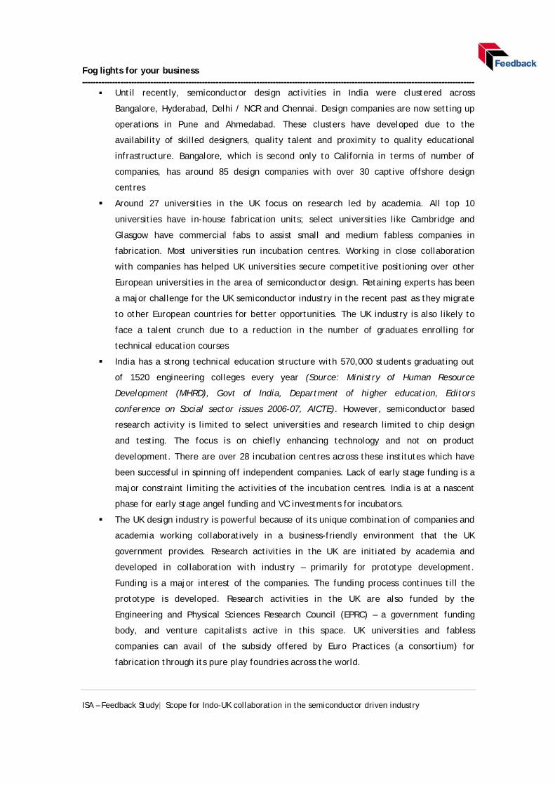
§ Until recently, semiconductor design activities in India were clustered across
Bangalore, Hyderabad, Delhi / NCR and Chennai. Design companies are now setting up
operations in Pune and Ahmedabad. These clusters have developed due to the
availability of skilled designers, quality talent and proximity to quality educational
infrastructure. Bangalore, which is second only to California in terms of number of
companies, has around 85 design companies with over 30 captive offshore design
centres
§ Around 27 universities in the UK focus on research led by academia. All top 10
universities have in-house fabrication units; select universities like Cambridge and
Glasgow have commercial fabs to assist small and medium fabless companies in
fabrication. Most universities run incubation centres. Working in close collaboration
with companies has helped UK universities secure competitive positioning over other
European universities in the area of semiconductor design. Retaining experts has been
a major challenge for the UK semiconductor industry in the recent past as they migrate
to other European countries for better opportunities. The UK industry is also likely to
face a talent crunch due to a reduction in the number of graduates enrolling for
technical education courses
§ India has a strong technical education structure with 570,000 students graduating out
of 1520 engineering colleges every year (Source: Ministry of Human Resource
Development (MHRD), Govt of India, Department of higher education, Editors
conference on Social sector issues 2006-07, AICTE). However, semiconductor based
research activity is limited to select universities and research limited to chip design
and testing. The focus is on chiefly enhancing technology and not on product
development. There are over 28 incubation centres across these institutes which have
been successful in spinning off independent companies. Lack of early stage funding is a
major constraint limiting the activities of the incubation centres. India is at a nascent
phase for early stage angel funding and VC investments for incubators.
§ The UK design industry is powerful because of its unique combination of companies and
academia working collaboratively in a business-friendly environment that the UK
government provides. Research activities in the UK are initiated by academia and
developed in collaboration with industry – primarily for prototype development.
Funding is a major interest of the companies. The funding process continues till the
prototype is developed. Research activities in the UK are also funded by the
Engineering and Physical Sciences Research Council (EPRC) – a government funding
body, and venture capitalists active in this space. UK universities and fabless
companies can avail of the subsidy offered by Euro Practices (a consortium) for
fabrication through its pure play foundries across the world.

Fog lights for your business ------------------------------------------------------------------------------------------------------------------------------------------------
ISA – Feedback Study| Scope for Indo-UK collaboration in the semiconductor driven industry
§ In contrast to the UK, research activities in India focusing on the area of Electronic
Design Automation are initiated by companies. Academia-industry collaboration for
research is not comprehensive. Industry funding for research is limited to providing
tools and lab equipment, and is not focussed on the entire life cycle of the project.
The impetus to become a major hub for the entire semiconductor value chain has
however begun in earnest with support from the Indian Government.
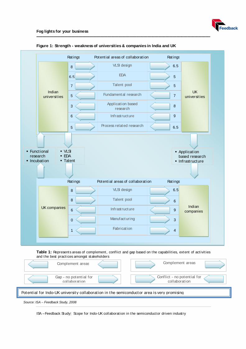
Conclusions and recommendations
The study reveals a synergy between India and the UK primarily in the areas of design, device
and applications. Figure 1 represents the strength and weakness of universities and companies
in India and the UK. Area of collaboration is derived based on the capabilities, extent of
activities, best practices followed across the counterparts in India and UK. For example, UK
universities score high in the areas of application based research, infrastructure and
fundamental research when compared to Indian universities. These are the complement areas
where Indian universities tend to gain out of the collaborations with the UK universities.
Similarly, there is scope for collaboration between the UK companies and the Indian
universities; the UK companies can look at local talent, EDA capabilities and VLSI design
expertise as the potential areas of collaboration. The direction of the arrow as shown in the
Table 1 shows the potential information flow between the counterparts in India and UK.
Arrows following one another indicates the potential areas for collaboration as they
complement each other. The arrows in two opposite directions indicate the gap – no potential
for collaboration and the arrows moving head on indicate the conflict areas – which mean
there is very little scope for collaboration, as each one is self-sufficient.
Fog lights for your business ------------------------------------------------------------------------------------------------------------------------------------------------
ISA – Feedback Study| Scope for Indo-UK collaboration in the semiconductor driven industry
Figure 1: Strength - weakness of universities & companies in India and UK
Table 1: Represents areas of complement, conflict and gap based on the capabilities, extent of activities and the best practices amongst stakeholders
UK companies
Fabrication
Manufacturing
Infrastructure
Talent pool
VLSI design
Indian companies
Potential areas of collaboration Ratings Ratings
6.5
6
9
3
4
8
8
6
0
1
Indian universities
UK universities
Potential areas of collaboration Ratings Ratings
5
5
7
8
9
6.5
8
6.5
7
5
3
6
5 Process related research
Infrastructure
Application based research
Fundamental research
Talent pool
EDA
VLSI design 6.5
Complement areas Complement areas
Gap – no potential for collaboration
Conflict – no potential for collaboration
§ VLSI § EDA § Talent
§ Application based research
§ Infrastructure
§ Functional research
§ Incubation
Potential for Indo-UK university collaboration in the semiconductor area is very promising
Source: ISA – Feedback Study, 2008

Fog lights for your business ------------------------------------------------------------------------------------------------------------------------------------------------
ISA – Feedback Study| Scope for Indo-UK collaboration in the semiconductor driven industry
Figure 2: Scope for collaboration between Indian and UK universities
UK universitie
Indian universiti
• Faster prototyping
• Access to
quality talent
• Access to advanced tools and facilities for research
• Scope to work
on next level technology
Areas of collaboration Benefit Benefit
• VLSI design • EDA • Fundamental research • Application
research • Talent pool • Infrastructure • Embedded systems
· Academia initiated research – primary focus
· Limited number of students engaged in design
· Strength lies is fundamental research
· State of the art infrastructure; strong government support
· Chip design and testing · Embedded systems · Core strengths lie in VLSI
design, modelling and simulation
· Strong analytical skill sets
· Quality of talent pool · Quality of educational
infrastructure
Ø Assistance on
VLSI design and analytical skills from Indian Universities
Ø Student Academia Internship programme
Ø Access to specialised labs based in UK
UK universities Indian universities Benefit analysis
Knowledge transfer through university exchange programmes and funding by industry & Government will be critical to success
Source: ISA – Feedback Study, 2008
Fog lights for your business ------------------------------------------------------------------------------------------------------------------------------------------------
ISA – Feedback Study| Scope for Indo-UK collaboration in the semiconductor driven industry
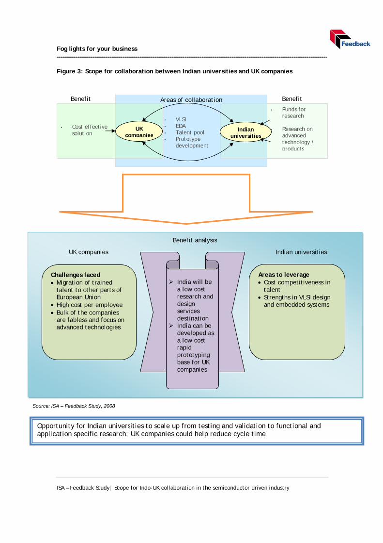
Figure 3: Scope for collaboration between Indian universities and UK companies
UK companies
Indian universities
• Cost effective solution
• Funds for research
• Research on
advanced technology / products
• VLSI • EDA • Talent pool • Prototype
development
Benefit Benefit Areas of collaboration
Challenges faced · Migration of trained
talent to other parts of European Union
· High cost per employee · Bulk of the companies
are fabless and focus on advanced technologies
Areas to leverage · Cost competitiveness in
talent · Strengths in VLSI design
and embedded systems
Ø India will be
a low cost research and design services destination
Ø India can be developed as a low cost rapid prototyping base for UK companies
UK companies Indian universities
Benefit analysis
Opportunity for Indian universities to scale up from testing and validation to functional and application specific research; UK companies could help reduce cycle time
Source: ISA – Feedback Study, 2008

Fog lights for your business ------------------------------------------------------------------------------------------------------------------------------------------------
ISA – Feedback Study| Scope for Indo-UK collaboration in the semiconductor driven industry
Figure 4: Scope for collaboration between Indian and UK companies
UK companies
Indian companies
• Talent cost advantage
• Availability of
trained designers
• Scope to work on advanced tools
• Scope to work
on application specific research
• VLSI • Embedded systems • Hardware/ board
design • Talent pool • Knowledge transfer
on technology tools
Areas of collaboration Benefit Benefit
Challenges faced · Talent crunch; high cost
of manpower · Large number of design
(fabless) companies
Areas to leverage · Availability of talent with
potential to deliver on application research
· Small start ups, currently focussing on circuit design and CAD simulation
Ø India will be
a low cost research and product development destination
UK companies Indian companies
Benefit analysis
Indian & UK companies could complement each others’ strengths for faster product development
Source: ISA – Feedback Study, 2008

Fog lights for your business ------------------------------------------------------------------------------------------------------------------------------------------------
ISA – Feedback Study| Scope for Indo-UK collaboration in the semiconductor driven industry
Figure 5: Scope for collaboration between Indian companies and UK universities
UK universities
Indian companies
• Funding advantage
• Application specific product research
• Faster
prototype development
• Application specific research
• Infrastructure (fabs and labs)
Areas of collaboration Benefit Benefit
· State of the art infrastructure
· Application specific research focus
· Focus on products for current market needs rather than futuristic technologies
Ø Indian
companies will have access to state of art infrastructure for product development
UK universities Indian companies Benefit analysis
Indian companies could leverage strengths of UK universities for state-of-the-art research
Source: ISA – Feedback Study, 2008
Fog lights for your business ------------------------------------------------------------------------------------------------------------------------------------------------
ISA – Feedback Study| Scope for Indo-UK collaboration in the semiconductor driven industry
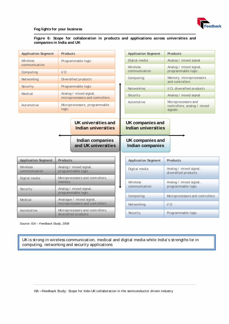
Figure 6: Scope for collaboration in products and applications across universities and companies in India and UK
Microprocessors, programmable logic
Automotive
Analog / mixed signal, microprocessors and controllers
Medical
Programmable logic Security
Diversified products Networking
I/O Computing
Programmable logic Wireless communication
Products Application Segment
Microprocessors and controllers, analog / mixed signals
Automotive
Analog / mixed signal Security
I/O, diversified products Networking
Memory, microprocessors and controllers
Computing
Analog / mixed signal, programmable logic
Wireless communication
Analog / mixed signal Digital media
Products Application Segment
Programmable logic Security
I/O Networking
Microprocessors and controllers Computing
Analog / mixed signal, programmable logic
Wireless communication
Analog / mixed signal, diversified products
Digital media
Products Application Segment
Microprocessors and controllers, memory
Digital media
Microprocessors and controllers, diversified products
Automotive
Analogue / mixed signal, microprocessors and controllers
Medical
Analog / mixed signal, programmable logic
Security
Analog / mixed signal, programmable logic
Wireless communication
Products Application Segment
UK companies and Indian companies
Indian companies and UK universities
UK universities and Indian universities
UK companies and Indian universities
UK is strong in wireless communication, medical and digital media while India’s strengths lie in computing, networking and security applications
Source: ISA – Feedback Study, 2008

Fog lights for your business ------------------------------------------------------------------------------------------------------------------------------------------------
ISA – Feedback Study| Scope for Indo-UK collaboration in the semiconductor driven industry
Figure 7: Geographical clusters and scope for collaboration
Figure 7A: Geographical clusters and scope for collaboration
Bangalore § Top global cluster in
semiconductor design § Home for over 85
design companies with over 30 captive offshore design centres
§ Nearly 57% of the VLSI designers employed in the semiconductor design companies in this cluster (Source: Feedback study on hardware design professionals in the country, 2003-04)
India South East England § Focus on application
engineering in the semiconductor ecosystem
§ Prominent in hardware design
§ Led by foreign investments into UK
§ Regions: Oxford, Southampton, Surrey
East of England § Presence of
semiconductor design companies with focus on device and application based markets
§ Lead by UK owned public companies
§ Region: Cambridge
§ Talent availability to
work on semiconductor design
§ Rapid growth and development in semiconductors
§ Collaboration from design to application of semiconductors
UK
Source: ISA – Feedback Study, 2008
Source: ISA – Feedback Study, 2008
Fog lights for your business ------------------------------------------------------------------------------------------------------------------------------------------------
ISA – Feedback Study| Scope for Indo-UK collaboration in the semiconductor driven industry
Figure 7B: Geographical clusters and scope for collaboration Figure 7C: Geographical clusters and scope for collaboration
Hyderabad
§ Local talent § Local Government support § Likely to host India’s first
semicon-related manufacturing facilities
§ Educational infrastructure
India Scotland § Presence of local fabless
companies and leading US based companies
§ Strong government support
§ Successful in fostering domestic privately owned companies
§ Regions: Glasgow, Edinburgh, Dundee and Aberdeen
§ Local fab set up § Ideal cluster for research
on next level technology
UK
Delhi / NCR § Home for small start up
companies, which include design houses for semiconductors
§ Cluster with high entrepreneurship drive
§ Cash rich and high proximity to markets
§ 30% of the VLSI designers employed in this cluster (Source: Feedback study on hardware design professionals in India, 2003-04)
India South West England § Presence of fabless
semiconductor companies
§ Cluster has several start up companies
§ Companies focus on customized design, high speed architecture
§ Has attracted foreign owned public companies
§ Regions: Bristol, Bath, Plymouth and Gloucester
§ Access to markets, potential cluster for venture capitalist
§ Scope to collaborate on customized design and high speed architecture
UK
Source: ISA – Feedback Study, 2008
Source: ISA – Feedback Study, 2008
Fog lights for your business ------------------------------------------------------------------------------------------------------------------------------------------------
ISA – Feedback Study| Scope for Indo-UK collaboration in the semiconductor driven industry
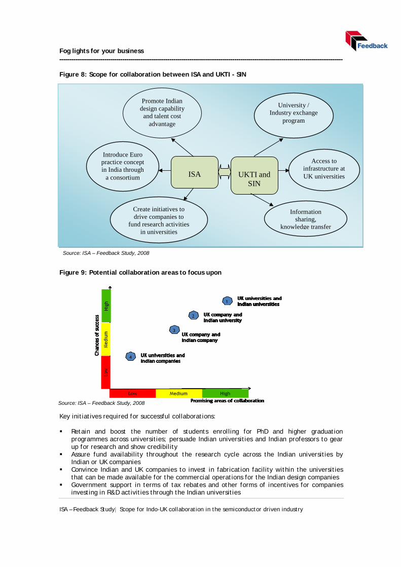
Figure 8: Scope for collaboration between ISA and UKTI - SIN
Figure 9: Potential collaboration areas to focus upon
Key initiatives required for successful collaborations: § Retain and boost the number of students enrolling for PhD and higher graduation
programmes across universities; persuade Indian universities and Indian professors to gear up for research and show credibility
§ Assure fund availability throughout the research cycle across the Indian universities by Indian or UK companies
§ Convince Indian and UK companies to invest in fabrication facility within the universities that can be made available for the commercial operations for the Indian design companies
§ Government support in terms of tax rebates and other forms of incentives for companies investing in R&D activities through the Indian universities
Promote Indian design capability
and talent cost advantage
Introduce Euro practice concept in India through
a consortium
Create initiatives to drive companies to
fund research activities in universities
ISA
UKTI and
SIN
University / Industry exchange
program
Access to infrastructure at UK universities
Information sharing,
knowledge transfer
Source: ISA – Feedback Study, 2008
Source: ISA – Feedback Study, 2008

Fog lights for your business ------------------------------------------------------------------------------------------------------------------------------------------------
ISA – Feedback Study| Scope for Indo-UK collaboration in the semiconductor driven industry
2. India semiconductor market details

Fog lights for your business ------------------------------------------------------------------------------------------------------------------------------------------------
ISA – Feedback Study| Scope for Indo-UK collaboration in the semiconductor driven industry
2.1 India semiconductor market overview
The middle class population is estimated to grow from 360 mn in 2006 to 525 mn in 2010. The annual household income for this class is between USD 10,000 to 55,500 (Source: India Brand Equity Forum, IBEF). This class is driving the electronic products market in India which has been estimated at USD 16.1 billion in 2006-07 (Source: Electronics Component Manufacturers Association). India's total semiconductor consumption is estimated at USD 3.46 billion in 2007–08 (Source: ISA- Frost Update Report 2007/08) primarily serviced by imports. The local manufacturing base is inadequate to cater to the domestic demand, which is increasing at 26% per annum. Prominent global semiconductor companies have been present in India for a while and operate through liaison offices, sales and marketing offices, design houses and/or through a well entrenched network of distributors and resellers. India has emerged as a strong base for R&D centres. Indian Design Centres or IDCs have graduated from executing small projects to driving critical ones. It is becoming increasingly common to find leading edge designs for the global market being driven by these IDCs. In addition, IDCs provide global support on tools and methodology. The design market has grown significantly due to the increasing number of international companies setting up offshore design and development centres in India and through expansion of current centres. Triggers for these activities include the following:
· Market need for regular introduction of new product variants / models has forced original equipment manufacturers (OEMs) / product companies to seek reduction in product development cycle time through outsourcing arrangements
· Declining margins and R&D budgets have driven companies to look for cost effective solutions without compromising on the quality of work
· Availability of a large base of engineering workforce coupled with their proficiency in English have made India an attractive destination for design and development
· Electronic design automation (EDA) companies (both product and services) are the starting block for the VLSI and hardware board design market. EDA companies have taken the lead in developing engineering human resource for the industry in India.
Figure 10: Structure of the semiconductor industry in India
Semiconductor Product Market
Semiconductor Device
Manufacturing
Semiconductor Design Services
• Semiconductor design continues to remain a core strength of India
• As per industry leaders, around 150 companies which specialize in VLSI design, embedded systems and hard ware / board level design are present in India
• VLSI design, hardware / board design, embedded systems market is estimated at USD 6.08 bn
• There is limited semiconductor manufacturing activity in India at present. Currently, India has no commercial wafer fab plants
· Design houses in India get chips fabricated at TSMC, SMIC and other pure play foundries
• Five major application segments contribute to the semiconductor demand in India
- Telecom - IT and Office Automation - Electronics - Industrial - Automotive
• Telecom, IT and Electronics are the high growth areas, accounting for 85%1 of total demand
• Consumption of semiconductors is estimated at USD 3.46 bn in 2007 – 081
1 Based on ISA – Frost Sullivan Update Report 2007 / 08 Source: ISA – Feedback Study, 2008

Fog lights for your business ------------------------------------------------------------------------------------------------------------------------------------------------
ISA – Feedback Study| Scope for Indo-UK collaboration in the semiconductor driven industry
2.1.1 Semiconductor design services The Indian semiconductor industry is dominated by players engaged in chip design. The semiconductor design space in the country consists of VLSI design, board design and embedded system companies - India has around 150 chip design companies (both Indian and subsidiaries of US and European chip firms), with almost all global semiconductor design companies having a presence here. Industry leaders believe that India is becoming a ‘design store’ with strengths in intellectual property (IP) development, integration and embedded system services. The ISA – IDC Report 2008 estimates the integrated chip design workforce in India to be around 130,000 while those working on embedded software total around 107,000. VLSI design From an electronics design perspective, the market can be divided into three segments: · The first segment comprises global MNCs and market makers who employ around 14,000
designers. They are associated with design chain methodology and the challenges associated with shrinking process nodes (65 nm and below)
· The second segment is shared by two domains: ‘pure play’ design services companies and fabless semiconductor companies. Over the last decade, multinationals have been associated with Indian service companies for complex projects in the design chain. Design services companies have moved up the value chain and bagged prestigious projects that have a worldwide impact
· The third segment is the Government including defence and space, with an increased focus on communication and defence products. The R&D centres of these organisations are producing complex designs.
VLSI design activities are clustered in four major cities of India. Bangalore is the biggest cluster, followed by Hyderabad, Delhi NCR and Chennai. Bangalore has around 85 of the 150 firms (including multinationals) engaged in chip design in India – making it one of the major global clusters in chip design along with the Silicon Valley, Cambridge (UK) and Taiwan. India is also emerging as the hotbed of wireless IC design with around 38% of Indian designers working on designs targeting wireless and mobile applications, compared to around 22% in Europe. (Source: India Brand Equity Forum, IBEF) Currently, product design involves IC design, board design and embedded software development – all done in conjunction with each other. The traditional separation between software digital logic analog and PCB is rapidly breaking down resulting in design convergence. This industry is witnessing rapid changes in technology – moving towards 65 nm geometry.
Embedded system design India’s strength in embedded design is reflected in its expertise in handling hardware and embedded design required to support lower power nodes. An increase in the number of international companies establishing their offshore centres in India has in turn spurred growth in Indian design services. Global majors have also shown confidence in the capabilities of Indian design companies by awarding them critical projects. India’s competitive edge in the global market is its talent base with design capabilities. Global companies are aware of the availability of this talent pool and are leveraging it effectively.
Fog lights for your business ------------------------------------------------------------------------------------------------------------------------------------------------
ISA – Feedback Study| Scope for Indo-UK collaboration in the semiconductor driven industry
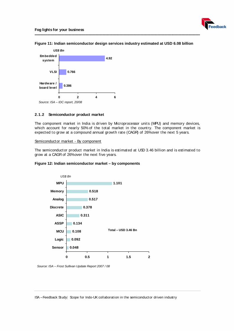
Figure 11: Indian semiconductor design services industry estimated at USD 6.08 billion
2.1.2 Semiconductor product market The component market in India is driven by Microprocessor units (MPU) and memory devices, which account for nearly 50% of the total market in the country. The component market is expected to grow at a compound annual growth rate (CAGR) of 26% over the next 5 years. Semiconductor market - By component The semiconductor product market in India is estimated at USD 3.46 billion and is estimated to grow at a CAGR of 26% over the next five years. Figure 12: Indian semiconductor market – by components
0.386
0.766
4.92
0 2 4 6
Hardware /board level
VLSI
Embeddedsystem
US$ Bn
Source: ISA – IDC report, 20/08
0.048
0.092
0.108
0.134
0.311
0.378
0.517
0.518
1.101
0 0.5 1 1.5 2
Sensor
Logic
MCU
ASSP
ASIC
Discrete
Analog
Memory
MPU
Total – USD 3.46 Bn
US$ Bn
Source: ISA – Frost Sullivan Update Report 2007 / 08
Fog lights for your business ------------------------------------------------------------------------------------------------------------------------------------------------
ISA – Feedback Study| Scope for Indo-UK collaboration in the semiconductor driven industry
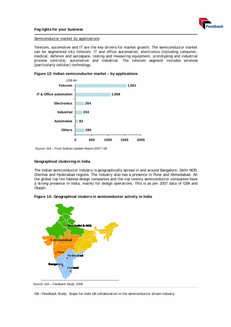
Semiconductor market by applications Telecom, automotive and IT are the key drivers for market growth. The semiconductor market can be segmented into telecom; IT and office automation; electronics (including consumer, medical, defence and aerospace, testing and measuring equipment, prototyping and industrial process controls); automotive and industrial. The telecom segment includes wireless (particularly cellular) technology. Figure 13: Indian semiconductor market – by applications Geographical clustering in India The Indian semiconductor industry is geographically spread in and around Bangalore, Delhi NCR, Chennai and Hyderabad regions. The industry also has a presence in Pune and Ahmedabad. All the global top ten fabless design companies and the top twenty semiconductor companies have a strong presence in India, mainly for design operations. This is as per 2007 data of GSA and iSuppli.
Figure 14: Geographical clusters in semiconductor activity in India
280
82
204
264
1,068
1,561
0 500 1000 1500 2000
Others
Automotive
Industrial
Electronics
IT & Office automation
Telecom
US$ Mn
Source: ISA – Frost Sullivan Update Report 2007 / 08
Source: ISA – Feedback Study, 2008
Fog lights for your business ------------------------------------------------------------------------------------------------------------------------------------------------
ISA – Feedback Study| Scope for Indo-UK collaboration in the semiconductor driven industry
These clusters have developed due to the availability of skilled designers in the vicinity. Availability of talent, educational infrastructure, support structure and allied units are the key characteristics of these clusters. The presence of both Indian and global firms has helped these clusters attain high technology orientation and also attract more semiconductor firms. Table 2: Geographic clusters and their characteristics Clusters Characteristics Remarks
Bangalore § Top global cluster in semiconductor design o Home to over 85 design companies
including nearly 30 captive offshore design centres
§ Nearly 57% of the VLSI designers are working in the cluster in the field of VLSI; second only to California (Source: Feedback Study on hardware professionals in the country, 2003-04)
Growing semiconductor ecosystem, strong IP protection, talent availability and cost advantage – key factors contributing to the growth of Bangalore as a major semiconductor design cluster in the world
Hyderabad § Known for technology orientation § Local talent § Support from the Government § Base for small and mid sized firms § Promoted as “Fab city” of India
India’s first fab facility likely to be established in Hyderabad. Has a supportive Government that is proactive in promoting fresh investments
Delhi NCR § Home to small start up firms including design houses for semiconductors
§ Composed primarily of entrepreneurs § One of the affluent regions in India
This is a promising cluster with a high growth potential.
Pune § Majority of the companies here are into digital media and animation
§ Access to a large talent pool § Good educational infrastructure
Being a leading educational hub in India with a large talent pool, Pune is an ideal location to base research activities
Source: ISA – Feedback Study, 2008
Fog lights for your business ------------------------------------------------------------------------------------------------------------------------------------------------
ISA – Feedback Study| Scope for Indo-UK collaboration in the semiconductor driven industry
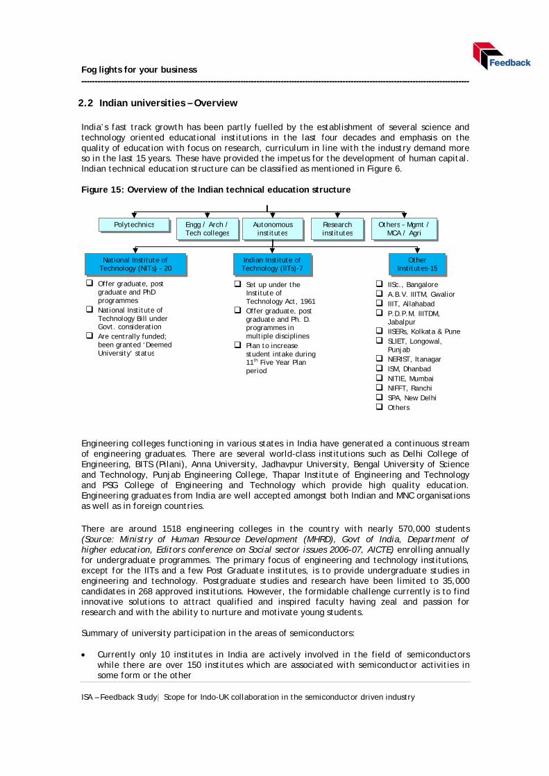
2.2 Indian universities – Overview India’s fast track growth has been partly fuelled by the establishment of several science and technology oriented educational institutions in the last four decades and emphasis on the quality of education with focus on research, curriculum in line with the industry demand more so in the last 15 years. These have provided the impetus for the development of human capital. Indian technical education structure can be classified as mentioned in Figure 6. Figure 15: Overview of the Indian technical education structure
Engineering colleges functioning in various states in India have generated a continuous stream of engineering graduates. There are several world-class institutions such as Delhi College of Engineering, BITS (Pilani), Anna University, Jadhavpur University, Bengal University of Science and Technology, Punjab Engineering College, Thapar Institute of Engineering and Technology and PSG College of Engineering and Technology which provide high quality education. Engineering graduates from India are well accepted amongst both Indian and MNC organisations as well as in foreign countries. There are around 1518 engineering colleges in the country with nearly 570,000 students (Source: Ministry of Human Resource Development (MHRD), Govt of India, Department of higher education, Editors conference on Social sector issues 2006-07, AICTE) enrolling annually for undergraduate programmes. The primary focus of engineering and technology institutions, except for the IITs and a few Post Graduate institutes, is to provide undergraduate studies in engineering and technology. Postgraduate studies and research have been limited to 35,000 candidates in 268 approved institutions. However, the formidable challenge currently is to find innovative solutions to attract qualified and inspired faculty having zeal and passion for research and with the ability to nurture and motivate young students. Summary of university participation in the areas of semiconductors: · Currently only 10 institutes in India are actively involved in the field of semiconductors
while there are over 150 institutes which are associated with semiconductor activities in some form or the other
Engg / Arch / Tech colleges
Research institutes
Others – Mgmt / MCA / Agri
Autonomous institutes
Indian Institute of Technology (IITs)-7
National Institute of Technology (NITs) – 20
Other Institutes-15
Polytechnics
q Set up under the Institute of Technology Act, 1961
q Offer graduate, post graduate and Ph. D. programmes in multiple disciplines
q Plan to increase student intake during 11th Five Year Plan period
q IISc., Bangalore q A.B.V. IIITM, Gwalior q IIIT, Allahabad q P.D.P.M. IIITDM,
Jabalpur q IISERs, Kolkata & Pune q SLIET, Longowal,
Punjab q NERIST, Itanagar q ISM, Dhanbad q NITIE, Mumbai q NIFFT, Ranchi q SPA, New Delhi q Others
q Offer graduate, post graduate and PhD programmes
q National Institute of Technology Bill under Govt. consideration
q Are centrally funded; been granted ‘Deemed University’ status
Fog lights for your business ------------------------------------------------------------------------------------------------------------------------------------------------
ISA – Feedback Study| Scope for Indo-UK collaboration in the semiconductor driven industry
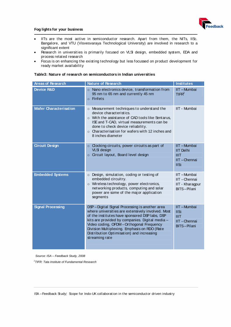
· IITs are the most active in semiconductor research. Apart from them, the NITs, IISc. Bangalore, and VTU (Visvesvaraya Technological University) are involved in research to a significant extent
· Research in universities is primarily focused on VLSI design, embedded system, EDA and process related research
· Focus is on enhancing the existing technology but less focussed on product development for ready market availability
Table3: Nature of research on semiconductors in Indian universities Areas of Research Nature of Research Institutes
Device R&D o Nano electronics device, transformation from 95 nm to 65 nm and currently 45 nm
o Finfets
IIT – Mumbai TIFR2
Wafer Characterisation o Measurement techniques to understand the device characteristics.
o With the assistance of CAD tools like Sentarus, ISE and T-CAD, virtual measurements can be done to check device reliability.
o Characterisation for wafers with 12 inches and 8 inches diameter
IIT – Mumbai
Circuit Design o Clocking circuits, power circuits as part of VLSI design
o Circuit layout, Board level design
IIT – Mumbai IIT Delhi IIIT IIT – Chennai IISc
Embedded Systems o Design, simulation, coding or testing of embedded circuitry.
o Wireless technology, power electronics, networking products, computing and solar power are some of the major application segments
IIT – Mumbai IIT – Chennai IIT - Kharagpur BITS – Pilani
Signal Processing DSP – Digital Signal Processing is another area where universities are extensively involved. Most of the institutes have sponsored DSP labs, DSP kits are provided by companies. Digital media – Video coding, OFDM – Orthogonal Frequency Division Multiplexing. Emphasis on RDO (Rate Distribution Optimisation) and increasing streaming rate
IIT – Mumbai IISc IIIT IIT – Chennai BITS – Pilani
Source: ISA – Feedback Study, 2008 2TIFR: Tata Institute of Fundamental Research

Fog lights for your business ------------------------------------------------------------------------------------------------------------------------------------------------
ISA – Feedback Study| Scope for Indo-UK collaboration in the semiconductor driven industry
2.2.1 Incubation centres Current status Incubation centres are operational at the IISc in Bangalore and in all the IITs in India. These have been set up by the faculty and alumni. Start-up units are spun off after a 2–3 year incubation period. Funding assistance for these start-ups is provided by the institutes and the alumni association. In India, TBIs (Technology Business Incubators) can play an important role in facilitating research. Such incubation centres in the US are known to add value to the institute and the company. They have enabled academic institutes to augment financial resources while pursuing their research activities. Many successful companies were set up and nurtured in this environment. In order to enable speedy commercialisation of R&D and establish closer links between R&D institutes, academia, and industry, the Department of Science and Technology (DST), Government of India, has set up 28 TBIs at various Indian institutes. Activity The start-up units are provided all facilities at the institute including space in the building/ university campus for research work. The focus of these units is to develop a patent which is commercially saleable in the market, after which the units are spun off from the universities. TBIs provide the start-up businesses with mentorship, incubation, patenting and external funding support. They create a research-friendly environment through the following activities:
· Initiating industry – funded projects: TBIs help faculty members undertake R&D projects on individual or joint proposals.
· Setting up work groups: TBIs help set up dedicated work groups that undertake multiple projects in areas that have research potential, particularly from the point of view of industry requirements.
· Establishing joint R&D centres: TBIs help in the establishment of joint R&D centres with help from industry or the government.
· Providing support to start ups: Entrepreneurs with ideas can start research at incubation centres, while simultaneously working on establishing their own set –up. Support provided by such incubation centres include:
o Administrative support and office facilities o Expertise in legal, financial, business and technical fields o Commercial support, i.e. access to market research, liaising with venture
capitalists, etc. Trends In the past, a few units have been spun off through this process. Most of these units were design based, with project orders from Indian or global companies. One of the major factors limiting the incubation activity is the initial funding requirements. India is at a nascent phase for early stage angel funding and venture capital investments for incubators.

Fog lights for your business ------------------------------------------------------------------------------------------------------------------------------------------------
ISA – Feedback Study| Scope for Indo-UK collaboration in the semiconductor driven industry
Table 4: Indicative list of active incubators in Indian institutes: Sr. No
Institute Incubator name Year of establishment
1. IIT Kharagpur Science and Technology Entrepreneurs Parks 1982
2. NIT Trichy Science and Technology Entrepreneurs Parks 1983
3. IISc Bangalore Society for Innovation and Development 1991
4. PSG Coimbatore Science and Technology Entrepreneurs Parks 1998 5. IIT Delhi Technology Business Incubator 2000
6. IIT Mumbai Society for Innovation and Entrepreneurship 2005
7. BITS – Pilani Technology Business Incubator -
8. IIT Chennai Technology Business Incubator - Table 5: Indicative list of successful start-ups: Sr. No.
Institute Company Field
1. IISc Bangalore PicoPeta Simputers Pvt. Ltd. Hardware and Software solutions for various business domains
2. IISc Bangalore Esquibe Communication Solutions Pvt. Ltd
IP creation in sensors, signals and systems
3. IIT Mumbai Powai Labs Technology Technologies Pvt. Ltd
EDA
4. IIT Mumbai Embedded Robot Technologies Pvt. Ltd
Artificial vision software protocol
5. IIT Chennai Neuro Synaptics IP creation and solutions in the area of neuro technology
6. IIT Chennai Midas Communication Technologies
Telecommunication solutions
7. PSG Coimbatore Onspec - Legend VLSI design Outlook Incubation activity in Indian universities has recorded an increase with Venture Capitalists showing interest in small start-ups. These VCs, most of them based in the Silicon Valley in the US, typically visit India once a month to meet entrepreneurs and research professors for discussions on the semiconductor activity in the country. Incubation activity is likely to come up in the NITs in the future. In an effort to encourage entrepreneurship skills among students, IIT Kharagpur has proposed to start a School of Entrepreneurship from the academic year 2008. Up to twenty students interested in starting a business would be admitted through the Joint Entrance Examination mode (IIT – JEE) and will be provided training in management, finance and innovation, in addition to the regular B.Tech course.
Source: ISA – Evalueserve Study, 2008
Source: ISA – Evalueserve Study, 2008
Fog lights for your business ------------------------------------------------------------------------------------------------------------------------------------------------
ISA – Feedback Study| Scope for Indo-UK collaboration in the semiconductor driven industry
2.2.2 University - industry collaboration in India Current status Semiconductor research activity in Indian universities is primarily driven by industry initiatives to work on specific areas in semiconductors. Industry has been striving constantly to help students and research graduates get practical experience in new technology platforms. Most of the companies supply design, testing and simulation tools to universities to encourage the use of current market driven technologies. University – industry research collaboration model This model was initiated in India by some of the bigger names in the Indian Semiconductor Industry. Texas Instruments and Intel are trend setters and have funded universities to set up labs. Companies like Cadence and ARM assist universities with specific tools which help groom students to meet industry expectations and standards. The VLSI Design Tools and Technology (VDTT), Advanced VLSI Design Lab and Nano Electronics Design Centre are some of the industry – university initiatives started to improve the scope of semiconductor research in India. At present, VLSI design is the most popular research area. Most often, companies either fund the institutes or supply development kits and tools necessary for research activity. Design tools are supplied either free of cost or at highly subsidised rates to provide access to the latest technology design and simulation tools. The research leads, who are usually professors, make proposals to indicate the required funding and the number of students for the research project. The period of collaboration depends on the intensity of research and typically ranges from 7 – 8 months to 3 years. The scope of industry – university research is currently very limited with industry just facilitating research and not investing heavily into it. Emphasis is on applied research and not much on business aspects. Training and support also form key features of such collaborative efforts. A few companies have introduced training programmes for the faculty and students.
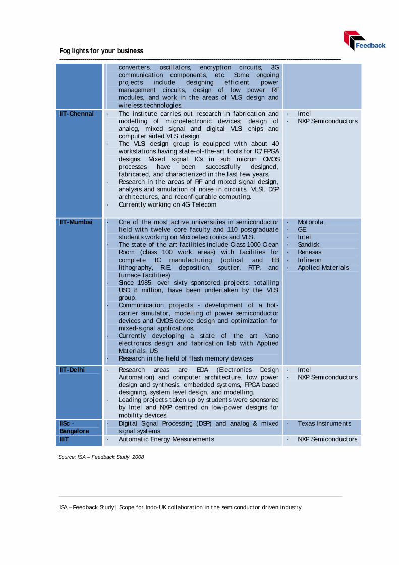
Table 6: Instances of university - industry collaboration in the area of semiconductors
Note: This is an indicative list compiled from available data
Institutes Research areas, research infrastructure Corporate alliance
IIT-Kharagpur
· Microelectronics and VLSI are the major areas of research
· The Advanced CAD Lab at IIT Kharagpur is one of its kind in India and is currently running several projects sponsored by various national and international agencies such as the Ministry of Information Technology, DRDO and ISRO. The projects encompass the design and implementation of digital and mixed-signal chips for various applications related to digital signal processing, image processing and communication system.
· The Advanced VLSI Design Lab (AVDL) is promoted by the IIT Foundation along with National Semiconductor, Sun Microsystems, Cadence Design, Synopsys, and Agilent Technologies. Projects include DC-DC
· Intel · IHP, Germany · National
Semiconductor · Sun Microsystems
Cadence Design Systems
· Synopsys · Agilent
Technologies
Fog lights for your business ------------------------------------------------------------------------------------------------------------------------------------------------
ISA – Feedback Study| Scope for Indo-UK collaboration in the semiconductor driven industry
converters, oscillators, encryption circuits, 3G communication components, etc. Some ongoing projects include designing efficient power management circuits, design of low power RF modules, and work in the areas of VLSI design and wireless technologies.
IIT-Chennai · The institute carries out research in fabrication and modelling of microelectronic devices; design of analog, mixed signal and digital VLSI chips and computer aided VLSI design
· The VLSI design group is equipped with about 40 workstations having state-of-the-art tools for IC/FPGA designs. Mixed signal ICs in sub micron CMOS processes have been successfully designed, fabricated, and characterized in the last few years.
· Research in the areas of RF and mixed signal design, analysis and simulation of noise in circuits, VLSI, DSP architectures, and reconfigurable computing.
· Currently working on 4G Telecom
· Intel · NXP Semiconductors
IIT-Mumbai · One of the most active universities in semiconductor field with twelve core faculty and 110 postgraduate students working on Microelectronics and VLSI.
· The state-of-the-art facilities include Class 1000 Clean Room (class 100 work areas) with facilities for complete IC manufacturing (optical and EB lithography, RIE, deposition, sputter, RTP, and furnace facilities)
· Since 1985, over sixty sponsored projects, totalling USD 8 million, have been undertaken by the VLSI group.
· Communication projects - development of a hot-carrier simulator, modelling of power semiconductor devices and CMOS device design and optimization for mixed-signal applications.
· Currently developing a state of the art Nano electronics design and fabrication lab with Applied Materials, US
· Research in the field of flash memory devices
· Motorola · GE · Intel · Sandisk · Renesas · Infineon · Applied Materials
IIT-Delhi · Research areas are EDA (Electronics Design Automation) and computer architecture, low power design and synthesis, embedded systems, FPGA based designing, system level design, and modelling.
· Leading projects taken up by students were sponsored by Intel and NXP centred on low-power designs for mobility devices.
· Intel · NXP Semiconductors
IISc – Bangalore
· Digital Signal Processing (DSP) and analog & mixed signal systems
· Texas Instruments
IIIT · Automatic Energy Measurements · NXP Semiconductors
Source: ISA – Feedback Study, 2008
Fog lights for your business ------------------------------------------------------------------------------------------------------------------------------------------------
ISA – Feedback Study| Scope for Indo-UK collaboration in the semiconductor driven industry
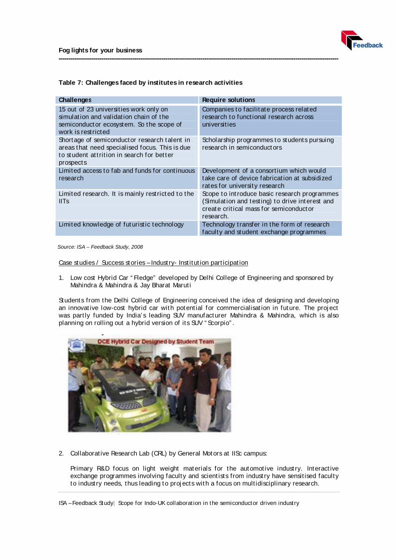
Table 7: Challenges faced by institutes in research activities
Challenges Require solutions
15 out of 23 universities work only on simulation and validation chain of the semiconductor ecosystem. So the scope of work is restricted
Companies to facilitate process related research to functional research across universities
Shortage of semiconductor research talent in areas that need specialised focus. This is due to student attrition in search for better prospects
Scholarship programmes to students pursuing research in semiconductors
Limited access to fab and funds for continuous research
Development of a consortium which would take care of device fabrication at subsidized rates for university research
Limited research. It is mainly restricted to the IITs
Scope to introduce basic research programmes (Simulation and testing) to drive interest and create critical mass for semiconductor research.
Limited knowledge of futuristic technology Technology transfer in the form of research faculty and student exchange programmes
Case studies / Success stories – Industry- Institution participation 1. Low cost Hybrid Car “Fledge” developed by Delhi College of Engineering and sponsored by
Mahindra & Mahindra & Jay Bharat Maruti
Students from the Delhi College of Engineering conceived the idea of designing and developing an innovative low-cost hybrid car with potential for commercialisation in future. The project was partly funded by India’s leading SUV manufacturer Mahindra & Mahindra, which is also planning on rolling out a hybrid version of its SUV “Scorpio”.
2. Collaborative Research Lab (CRL) by General Motors at IISc campus:
Primary R&D focus on light weight materials for the automotive industry. Interactive exchange programmes involving faculty and scientists from industry have sensitised faculty to industry needs, thus leading to projects with a focus on multidisciplinary research.
Source: ISA – Feedback Study, 2008
Fog lights for your business ------------------------------------------------------------------------------------------------------------------------------------------------
ISA – Feedback Study| Scope for Indo-UK collaboration in the semiconductor driven industry
3. CorDECT - a low-cost advanced Wireless Access System developed by Midas Communication
Technologies and IIT Madras, in association with Analog Devices, USA The technology provides complete wireless access solution with seamless integration of high quality voice and 35/70 kbps Internet access to its wireless subscribers. The technology is based on the DECT (Digitally Enhanced Cordless Telecommunication) air interface standard specification of the European Telecommunication Standards Institute (ETSI). In India, corDECT is manufactured under license by Crompton Greaves, Electronics Corporation of India Ltd (ECIL), HFCL and Shyam Telecom Ltd. One of most successful and early installations of corDECT has been in the African island nation of Madagascar. corDECT is operational in the city of Tamatave (formerly Toamasina) for over two years now, and subsequently it has been installed in the cities of Sambava and Anthala. Fiji Telecom installed corDECT to serve its subscribers in the island of Ba, far away from the capital Suva. In the course of the last couple of years, corDECT was tested by telecom standardisation bodies in Argentina, Brazil, Europe (ETSI), Kenya, Angola, Tunisia, Nigeria, and was cleared for induction in their respective networks. Currently, there are field trials underway in Iran, Egypt and Yemen. Commercial corDECT systems are also operational in Argentina, Brazil, Tunisia and Nigeria. Outside of India, corDECT is manufactured under licence by BBS Access in Singapore and by Omniacom in Tunisia. corDECT will soon be manufactured locally in Brazil too. (Source: Indian innovators association)
Fog lights for your business ------------------------------------------------------------------------------------------------------------------------------------------------
ISA – Feedback Study| Scope for Indo-UK collaboration in the semiconductor driven industry
2.3 Semiconductor Policy in India
To take advantage of potential economic opportunities and to also make India an attractive investment destination, the Government announced the Semiconductor Policy with attractive incentives so as to build capabilities to make it self-reliant in this sector. This was the first policy dedicated to the semiconductor industry in India and was announced on February 22, 2007.
2.3.1 Key highlights of the policy
· The grant of Special Economic Zone (SEZ) status · Enactment of Semiconductor Integrated Circuits Layout-Design Act, 2000 to provide for
protection of Semiconductor Integrated Circuits Layout-Designs · Incentive of 20% of the capital expenditure during the first 10 years for the units in SEZ
and 25% of the capital expenditure for non-SEZ units · Exemption from countervailing duty (CVD) for units in non-SEZ · The threshold Net Present Value (NPV) of investment has been pegged at USD 635.94
million and USD 254.36 million for semiconductor manufacturing (Fab units) products and for other eco-system products, respectively
· The policy has a special incentive package to attract investments for setting up semiconductor fabrication and other micro and nanotechnology manufacturing industries.
· The incentives will be for the manufacture of all semiconductors, displays including Liquid Crystal Displays (LCDs), Organic Light Emitting Diodes (OLED), Plasma Display Panels (PDP), any other emerging displays, storage devices, solar cells, photovoltaic other advanced micro and nanotechnology products
Table 8: Incentives for setting up a fab unit in SEZ location
Type of unit Threshold NPV of investments
Incentive in SEZ Incentive in Non-SEZ
Fab unit INR 2500 crore (USD 566 million)
20% 25% + exemption from CVD
Ecosystem unit INR 1000 crore (USD 266 million)
20% 25% + exemption from CVD
Note: (Incentive in % of capital expenditure); CVD is Countervailing Duty 2.3.2 Incentives for investors Any unit may claim incentives in the form of capital subsidy or equity participation in any combination of the following: · Capital equity in the project not exceeding 26% · Capital subsidy in the form of investment grant and interest subsidy · Those investors who choose equity as part of their incentive package shall be given such
equity after the financial closure of the project and the equity shall be released on a proportionate basis as equity is brought in by the promoters.
· All other incentives shall be released after the end of the financial year in which the NPV of the total investment exceeds the threshold value. Thereafter, the incentives shall be provided on an annual basis on the value of investments made during the year and be restricted to the first 10 years of the project life.
· The Special Incentive Package shall be available only up to March 31st, 2010.
Source: Government of India
Fog lights for your business ------------------------------------------------------------------------------------------------------------------------------------------------
ISA – Feedback Study| Scope for Indo-UK collaboration in the semiconductor driven industry
2.3.3 Benefits of the policy The semiconductor policy is primarily formed to facilitate device manufacturing in the semiconductor ecosystem. The growth in market volumes and the outlook to adapt newer technologies have provided impetus to the semiconductor industry in India. Currently, India imports a significant amount of semiconductors for its domestic market. With a view to making the country self sufficient, the policy is aimed at starting up fabrication, assembly and packing units in the country (ATMP – Assembly Test Mark Pack). 2.3.4 Challenges Significant investments are required for setting up fabrication units (around USD 2 billion per unit). This makes it difficult for a private entity to make the total investment and reap benefits; further, rapid technology upgrading requires continuous investments and with growing markets, sustainability of such fabs is tough. For commercial fabs to be operational, the companies need to look at global markets. 2.3.5 SMDP (Special Manpower Development Program) The industry body is actively involved in the Special Manpower Development Program, a government initiative with the private industry. The objective of the programme is to facilitate faculty training. The SMDP focuses on supplying kits to universities and encouraging VLSI as a part of the curriculum. Under the renewed version of the scheme 2007, nineteen new universities will be targeted, bringing the total to thirty two.

Fog lights for your business ------------------------------------------------------------------------------------------------------------------------------------------------
ISA – Feedback Study| Scope for Indo-UK collaboration in the semiconductor driven industry
2.4 Strengths and weaknesses of Indian universities and companies
2.4.1 Strength and weakness analysis of Indian universities in the field of semiconductors: Figure 16: Level of semiconductor activities in Indian Universities
Note: Research initiation by industry is higher than the universities as they provide the latter with the basic EDA tools and equipment Exhibit: Definitions Categories Variables Description Research activity
VLSI design Activities in the field of VLSI, FPGA design Process related research Research on device physics - alternate
materials, characterization Fundamental research Research activity on futuristic technology such
as 4G Telecom, Wimax, etc. EDA Modelling and simulation of devices, system Application based research Research on direct end products
Infrastructure and resources
Infrastructure Design labs and kits for research activities Source of funds Funds generated through university internal
accruals, government , companies Incubation Activities of incubation cell within the
university and number of successful launches. Talent pool Number of students pursuing semiconductor
research in universities Research initiative
University driven research Research initiated by university professors Company driven research Research initiated by companies
0 1 2 3 4 5 6 7 8 9
EDA
Application based research
Process related research
VLSI design
Talent pool
Source of funds
Company driven research
Fundamental research
University driven research
Incubation
Infrastructure
Extent of semiconductor research activities, support from companies and funding
Research initiative
High Low
Infrastructure and Resources Research Activities
Source: ISA – Feedback Study, 2008
Fog lights for your business ------------------------------------------------------------------------------------------------------------------------------------------------
ISA – Feedback Study| Scope for Indo-UK collaboration in the semiconductor driven industry
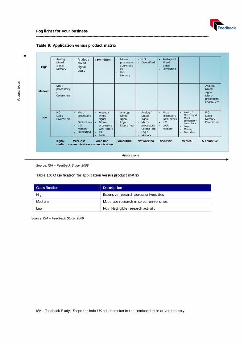
Table 9: Application versus product matrix
Table 10: Classification for application versus product matrix
Classification Description
High Extensive research across universities
Medium Moderate research in select universities
Low No / Negligible research activity
• I/O • Logic • Memory • Diversified
• Analog / Mixed signal
• Micro-processors / Controllers
• Logic • Memory • Diversified
• Micro-processors Controllers
• I/O • Logic • Memory
• Analog / Mixed signal
• Micro-processors Controllers
• Logic • Memory
• Analog / Mixed signal
• Logic • Diversified
• Analog / Mixed signal
• Micro-processors Controllers
• I/O • Logic
• Micro-processors / Controllers
• I/O • Memory • Diversified
• I/O • Logic • Diversified
• Analog / Mixed signal
• Micro-processors Controllers
• Micro-
processors / Controllers
• Analogue /
Mixed signal
• Diversified
• I/O • Diversified
• Micro-processors /Controllers
• I/O • Memory
Diversified • Analog / Mixed signal
• Logic
• Analog / Mixed Signal
• Memory
High
Medium
Low
Digital media
Wireless communication
Wire line communication
Computing Networking Security Medical Automotive
Applications
Pro
duct
focu
s
Source: ISA – Feedback Study, 2008
Source: ISA – Feedback Study, 2008
Fog lights for your business ------------------------------------------------------------------------------------------------------------------------------------------------
ISA – Feedback Study| Scope for Indo-UK collaboration in the semiconductor driven industry
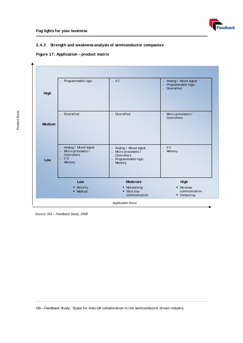
2.4.2 Strength and weakness analysis of semiconductor companies Figure 17: Application – product matrix
• I/O • Memory
• Analog / Mixed signal • Micro-processors /
Controllers • Programmable logic • Memory
• Analog / Mixed signal • Micro-processors /
Controllers • I/O • Memory
• Micro-processors / Controllers
• Diversified
• Diversified
• Analog / Mixed signal • Programmable logic • Diversified
• I/O
• Programmable logic
High
Low
High Moderate Low
§ Security § Medical
§ Networking § Wire line
communication
§ Wireless communication
§ Computing
Medium
Application focus
Pro
duct
focu
s
Source: ISA – Feedback Study, 2008
Fog lights for your business ------------------------------------------------------------------------------------------------------------------------------------------------
ISA – Feedback Study| Scope for Indo-UK collaboration in the semiconductor driven industry
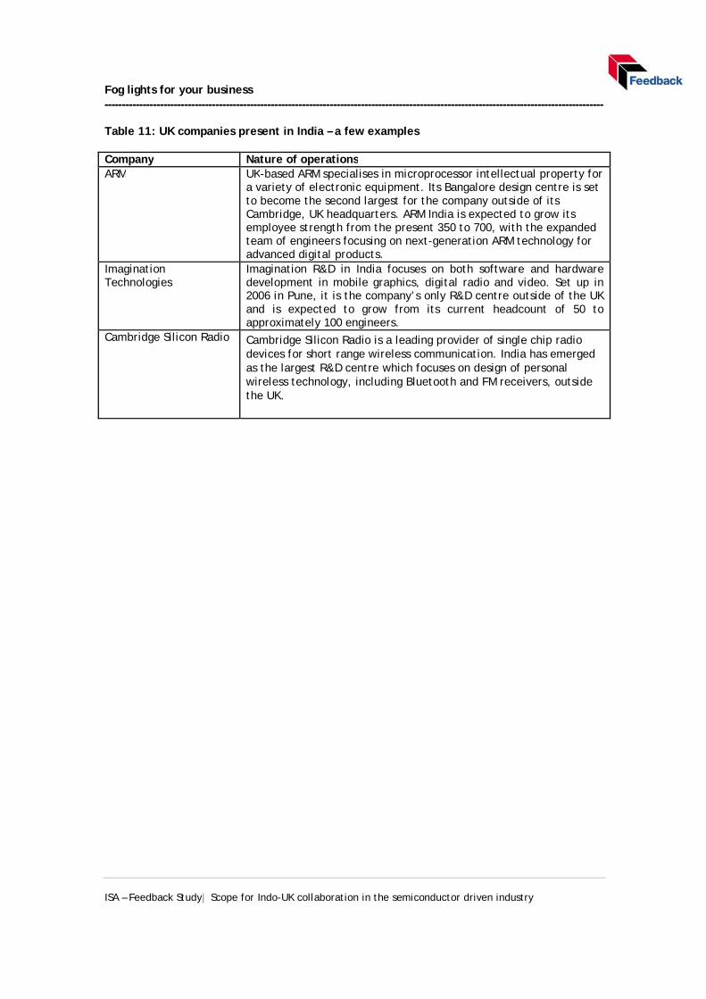
Table 11: UK companies present in India – a few examples Company Nature of operations ARM UK-based ARM specialises in microprocessor intellectual property for
a variety of electronic equipment. Its Bangalore design centre is set to become the second largest for the company outside of its Cambridge, UK headquarters. ARM India is expected to grow its employee strength from the present 350 to 700, with the expanded team of engineers focusing on next-generation ARM technology for advanced digital products.
Imagination Technologies
Imagination R&D in India focuses on both software and hardware development in mobile graphics, digital radio and video. Set up in 2006 in Pune, it is the company’s only R&D centre outside of the UK and is expected to grow from its current headcount of 50 to approximately 100 engineers.
Cambridge Silicon Radio Cambridge Silicon Radio is a leading provider of single chip radio devices for short range wireless communication. India has emerged as the largest R&D centre which focuses on design of personal wireless technology, including Bluetooth and FM receivers, outside the UK.

Fog lights for your business ------------------------------------------------------------------------------------------------------------------------------------------------
ISA – Feedback Study| Scope for Indo-UK collaboration in the semiconductor driven industry
3. UK semiconductor market details

Fog lights for your business ------------------------------------------------------------------------------------------------------------------------------------------------
ISA – Feedback Study| Scope for Indo-UK collaboration in the semiconductor driven industry
3.1 UK semiconductor industry overview
3.1.1 Overview of the semiconductor industry in the UK The UK houses operations of more than 500 semiconductor firms, 80% of which are foreign-owned. These firms employ close to 8,397 (Source: NMI design survey report 2006) engineering staff of which around 3,000 undertake design engineering related tasks. Around half of these focus on analog, RF, or mixed signal design. UK’s core competency in the semiconductor area lies in design and development of new devices. Prominent global semiconductor companies have design and support operations in the UK. Currently, only three specialised CMOS fabrication units are present here – there are no manufacturing and fabrication capabilities. Industrial, telecommunications, transport and consumer electronics account for 50% of the applications market in UK as depicted in the Figure 18. Mobile communication, consumer electronics, medical electronics, defence and automotive electronics are the major focus areas of design and development companies. Figure 18: Market breakdown (in percentage)
The UK market for communications, IT, and consumer electronics has continued to grow faster than that of other major European markets in recent years, as a result of which the UK market could soon become the leading EU market in this area. This growth is partly attributed to the emergence of London as an important financial hub globally and which has resulted in record inward investment into the UK and the ICT demands of these firms.
§ The UK IT market in 2007 was estimated at approximately USD 140 billion
§ The UK Communications market is growing faster than France, Germany and Italy; is estimated to be around USD 116 billion – second highest in value terms in 2007
§ The UK market for consumer electronics is the largest in EU; estimated at around USD 26 billion in 2007
The UK continues to boast of a world class microelectronics competency base. It is the combination of experience and competence that provides a compelling competitive position fuelling productivity and innovation. Anecdotal evidence supports this and shows that firms have quickly realized that costs can be saved in areas such as design implementation and verification. These firms will outsource or “insource” such functions– either locally or offshore - depending on their requirement. Many leading companies have located their design centres where competent talent is available. This trend of trans-national design – design across
Source: NMI Design Survey Report 2006

Fog lights for your business ------------------------------------------------------------------------------------------------------------------------------------------------
ISA – Feedback Study| Scope for Indo-UK collaboration in the semiconductor driven industry
national boundaries, is now mainstream even amongst SME organisations. The trend favours the UK in at least two ways:
· It has maintained a high level of inward investment from foreign owned companies that recognise and tap into UK competencies
· Encouraged by the government policy, UK companies are led by free-market forces. This fosters a culture that seeks to exploit opportunity rather than fear change. UK companies are configuring their value-chains to exploit the trans-national aspect of design thus enabling them to compete better.
Business indicators
· Optimistic business outlook with an increase in the number of design start-ups is predicted for the coming year.
· Business model transformation – design services remain strong but the fabless model is the model of choice while IP is either a niche play or an augmentation to services.
· Companies have emerged from the downturn with greater optimism for the future · Firms have a stronger focus on markets and are better positioned to compete. · Partnerships
— Recognition that other regions and partnering can be used to improve product delivery, either by lowering costs or by utilising skills outside the UK
· Despite the confidence, the fact remains that microelectronics is not for the faint hearted. The competitiveness bar continues to get higher and companies still face many challenges in the market. Government, firms and individuals must continually work to sustain a competitive advantage.
Figure 19: Structure of the semiconductor industry in the UK
Semiconductor product market
Semiconductor device
manufacturing
Semiconductor design services
• Fabless design – focus areas for the companies engaged in semiconductor design in UK
• Nearly 400 companies focus primarily on design like VLSI, FPGA, CAD Tools development
• UK has a limited number of fabs which specialise in device fabrication
• Almost all the top seven universities in the UK have a fabrication setup for research purposes and these are also commercially available to companies with non complex designs
• Specialised device fabrication is done through IMEC and TSMC
• Industrial, telecommunications, transport and consumer electronics are the major application segments contributing to bulk of the semiconductors market
• These segments have grown significantly over the years and are expected to continue to grow due to rapid change in technology
• Medical and defence segments are expected to drive semiconductor market in UK in the future
Source: ISA – Feedback study, 2008

Fog lights for your business ------------------------------------------------------------------------------------------------------------------------------------------------
ISA – Feedback Study| Scope for Indo-UK collaboration in the semiconductor driven industry
3.1.2 Semiconductor design companies in the UK UK design companies have led the world in the knowledge of system level aspects of design and incorporation of knowledge into new and innovative products. With 400+ independent design houses, UK has more electronics system design houses than any other European nation. Large design houses such as Cambridge Consultants and Generics and Plextec, typically perform complete electronic system design using specialists with skills as diverse as RF design, semiconductor design and aesthetic and industrial design. Major companies in the Pacific Rim and USA benefit from the complete system design houses and many have been working with UK for long. Mobile communication, consumer electronics, medical electronics, defence electronics and automobile electronics are some markets where these companies have high presence. The ownership pattern of the companies can be any of the following (percentage indicates the structure based on the ownership of the companies in the UK; source: NMI Design Survey Report 2006)
· UK owned private (9%)
· UK owned public (11%)
· Foreign owned, UK limited (73%)
· Foreign owned public (7%)
The UK design industry is dominated by foreign owned companies with widespread leading edge digital and analog design activities. Major design strengths of UK based design companies are in wireless, digital media and communications applications. It is estimated (Source: NMI design survey report 2006) that the UK contributes approximately 15% of the total ASIC semiconductor design starts. Add to this, the many other semiconductor devices that are designed and manufactured here, and it shows that the UK has a very strong design capability. The UK electronics design industry is very powerful because of the unique network of companies and academia working interactively within a conducive business environment, ensured by the UK Government. UK designers work in a wide variety of companies: systems builders; captive and independent design houses; research establishments; CAD/EDA tool vendors; chip suppliers, including fabless and chipless semiconductor companies and technical distributors. Many also work on a freelance contract design basis. Excellence in system design, flows from all areas of the UK electronics industry. It is fostered in academic-based institutions such as the Institute for System Level Integration, associated with the Alba Centre, and the Mobile Virtual Centre of Excellence, and flourishes in design groups in industry. The strong academic base, and its ability to work closely with the industry, means that UK electronics designers will continue to lead the world as new and exciting technologies emerge from research into commercial reality, and as new design tools make the design process easier. Elements of the network also include:
· Equipment, system manufacturers and specialist component manufacturers with internal semiconductor design team
· Design houses and freelance designers offering third party design to clients · EDA / CAD tool vendors · IP developers and suppliers offering hardware and software building blocks to designers · Universities supplying qualified graduates and advanced research and development
Fog lights for your business ------------------------------------------------------------------------------------------------------------------------------------------------
ISA – Feedback Study| Scope for Indo-UK collaboration in the semiconductor driven industry
Designers within semiconductor suppliers Most major global semiconductor companies have a UK design and support operation while many also manufacture in the UK. Those that have built design operations in the UK include Alcatel, Analog Devices, Cypress, Dialog Semiconductor, Fujitsu, Infineon, Lattice Semiconductor, LSI Logic, Motorola, NEC, NXP, Renesas, Sony, STMicroelectronics and Texas Instruments. Companies that have created manufacturing facilities include Agilent, Atmel, International Rectifier, Motorola, National Semiconductor, X-Fab and Zarlink. The UK’s manufacturing expertise is in power, analog and RF wafer processing. While most of these design teams are engaged in developing standard parts, some offer their customers design services in ASIC devices across a range of technologies, including digital, analog and mixed signal. The UK’s particular strength in the design of RF chips has enabled a number of companies to become world players in advanced telecommunications. An extensive and mature network of electronic component distributors provides design help and technical support with qualified engineering staff, as well as a reliable supply of components. Fabless semiconductor companies While the companies mentioned above design and manufacture their chips in their own factories, many innovative semiconductor companies choose to design their own chips but have them manufactured by third party silicon foundries. Some of these companies have bases in the UK, including Altera, Cambridge Silicon Radio, Clearspeed Technology, CML, Elixent, Oxford Semiconductor, Icera Semiconductor, Phyworks, Swindon Silicon Systems, Wolfson and Xilinx. Most of these companies have in-house design teams, but a significant proportion supplements their skills by using the UK’s third party design network. Chipless semiconductor companies Over the past few years, the UK has seen dozens of small and innovative start-ups developing and marketing semiconductor intellectual property (IP). Some of these ‘chipless’ semiconductor firms have grown rapidly and have become internationally renowned. Cambridge-based ARM is the world’s number one IP core provider and its processors, designed and developed in the UK are, the processor cores of choice for telecom and networking applications. Virtually every major semiconductor company and many equipment companies have acquired licences to use ARM cores. This trend has done much to attract world-class companies to the UK, growing and evolving the electronics systems design sector. Newer UK companies, such as Amphion (now part of Conexant) and ARC, are now well on their way to emulating this success. Leading the field in reconfigurable processor cores, ARC is licensing its technology to companies worldwide. For example, Broadcom, Xilinx, Tektronix and TTPCom all work closely with ARC to produce world-beating products in areas as diverse as mobile communications and advanced test equipment. The UK also has strengths in Electronic Design Automation (EDA) and Computer Aided Design (CAD). Zuken is one of the oldest while Mentor Graphics and Cadence have been developing tools for nearly a decade. The UK also has a complete range of independent test houses that have the ability to assess products during the design phase so as to ensure compliance to international standards. Some of the major research initiative projects include:
· The Optonics consortium near South East London by Intel which focuses on shallow junction formation of silicon CMOS devices
· Plastic Electronics by Plastic Logic which will focus on the development of flexible materials like display technologies, Wi – Fi key boards
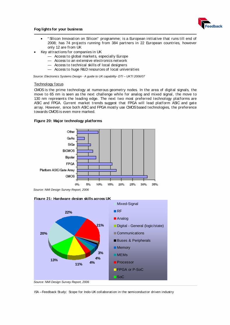
Fog lights for your business ------------------------------------------------------------------------------------------------------------------------------------------------
ISA – Feedback Study| Scope for Indo-UK collaboration in the semiconductor driven industry
· “Silicon Innovation on Silicon” programme; is a European initiative that runs till end of 2008; has 74 projects running from 384 partners in 22 European countries, however only 12 are from UK
· Key attractions for companies in UK — Access to global markets, especially Europe — Access to an extensive electronics network — Access to technical skills of local designers — Access to huge R&D resources of local universities
Technology focus
CMOS is the prime technology at numerous geometry nodes. In the area of digital signals, the move to 65 nm is seen as the next challenge while for analog and mixed signal, the move to 130 nm represents the leading edge. The next two most preferred technology platforms are ASIC and FPGA. Current market trends suggest that FPGA will lead platform ASIC and gate array. However, since both ASIC and FPGA mostly use CMOS based technologies, the preference towards CMOS is even more marked.
Figure 20: Major technology platforms
Figure 21: Hardware design skills across UK
(@@ pie totals 98%)
20%
22%
13%
3%
4%4%11%
21%
Mixed-Signal
RF
Analog
Digital - General (logic/state)
Communications
Buses & Peripherals
Memory
MEMs
Processor
FPGA or P-SoC
SoCSource: NMI Design Survey Report, 2006
Source: Electronics Systems Design - A guide to UK capability- DTI – UKTI 2006/07
Source: NMI Design Survey Report, 2006
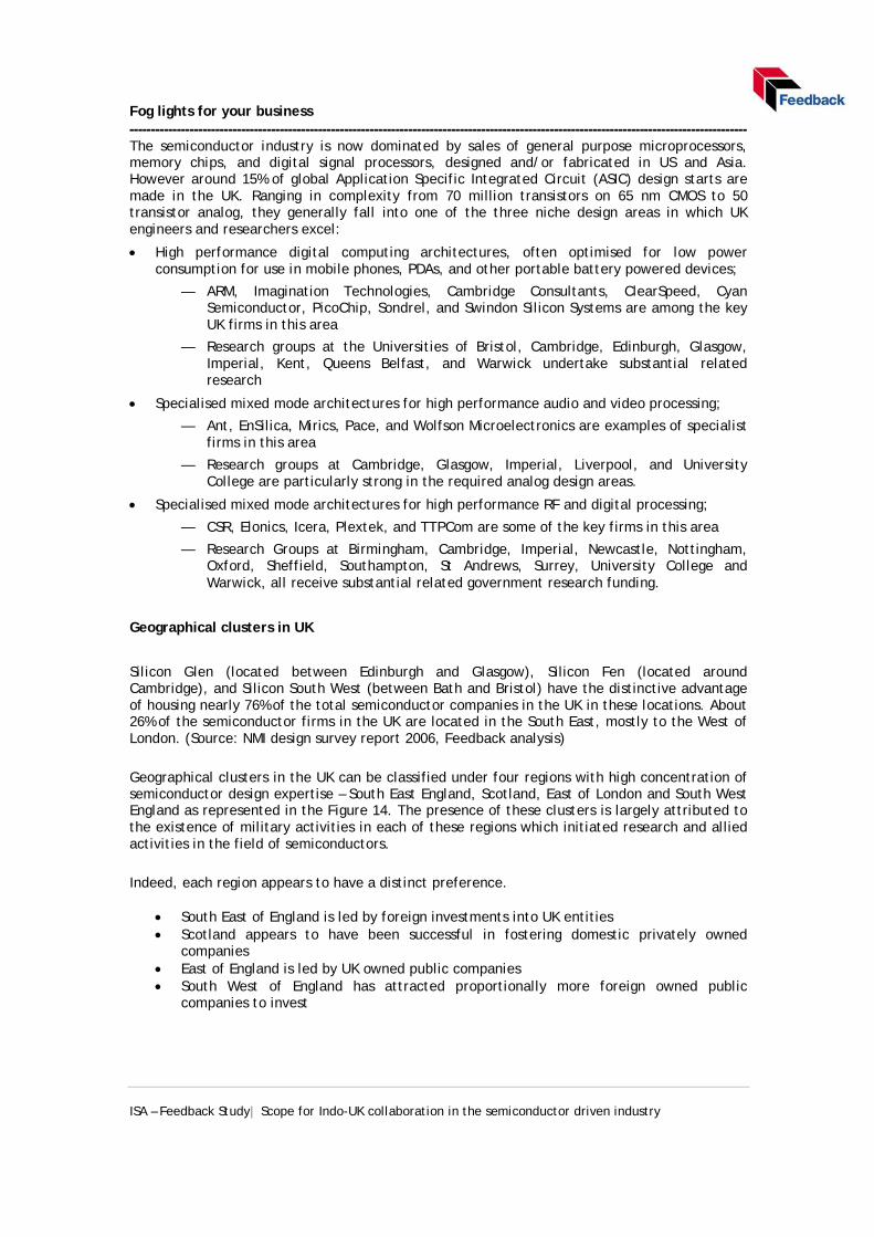
Fog lights for your business ------------------------------------------------------------------------------------------------------------------------------------------------
ISA – Feedback Study| Scope for Indo-UK collaboration in the semiconductor driven industry
The semiconductor industry is now dominated by sales of general purpose microprocessors, memory chips, and digital signal processors, designed and/or fabricated in US and Asia. However around 15% of global Application Specific Integrated Circuit (ASIC) design starts are made in the UK. Ranging in complexity from 70 million transistors on 65 nm CMOS to 50 transistor analog, they generally fall into one of the three niche design areas in which UK engineers and researchers excel:
· High performance digital computing architectures, often optimised for low power consumption for use in mobile phones, PDAs, and other portable battery powered devices;
— ARM, Imagination Technologies, Cambridge Consultants, ClearSpeed, Cyan Semiconductor, PicoChip, Sondrel, and Swindon Silicon Systems are among the key UK firms in this area
— Research groups at the Universities of Bristol, Cambridge, Edinburgh, Glasgow, Imperial, Kent, Queens Belfast, and Warwick undertake substantial related research
· Specialised mixed mode architectures for high performance audio and video processing;
— Ant, EnSilica, Mirics, Pace, and Wolfson Microelectronics are examples of specialist firms in this area
— Research groups at Cambridge, Glasgow, Imperial, Liverpool, and University College are particularly strong in the required analog design areas.
· Specialised mixed mode architectures for high performance RF and digital processing;
— CSR, Elonics, Icera, Plextek, and TTPCom are some of the key firms in this area
— Research Groups at Birmingham, Cambridge, Imperial, Newcastle, Nottingham, Oxford, Sheffield, Southampton, St Andrews, Surrey, University College and Warwick, all receive substantial related government research funding.
Geographical clusters in UK
Silicon Glen (located between Edinburgh and Glasgow), Silicon Fen (located around Cambridge), and Silicon South West (between Bath and Bristol) have the distinctive advantage of housing nearly 76% of the total semiconductor companies in the UK in these locations. About 26% of the semiconductor firms in the UK are located in the South East, mostly to the West of London. (Source: NMI design survey report 2006, Feedback analysis)
Geographical clusters in the UK can be classified under four regions with high concentration of semiconductor design expertise – South East England, Scotland, East of London and South West England as represented in the Figure 14. The presence of these clusters is largely attributed to the existence of military activities in each of these regions which initiated research and allied activities in the field of semiconductors.
Indeed, each region appears to have a distinct preference.
· South East of England is led by foreign investments into UK entities · Scotland appears to have been successful in fostering domestic privately owned
companies · East of England is led by UK owned public companies · South West of England has attracted proportionally more foreign owned public
companies to invest
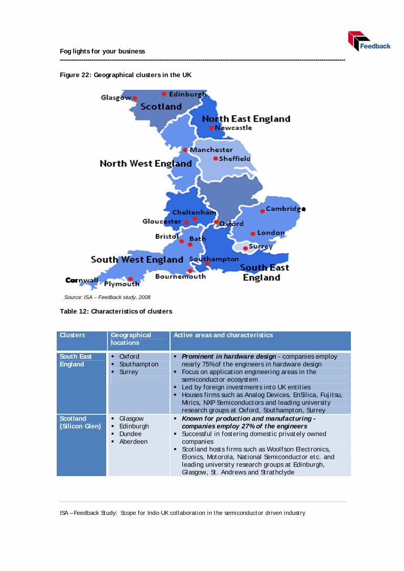
Fog lights for your business ------------------------------------------------------------------------------------------------------------------------------------------------
ISA – Feedback Study| Scope for Indo-UK collaboration in the semiconductor driven industry
Figure 22: Geographical clusters in the UK
Table 12: Characteristics of clusters Clusters Geographical
locations Active areas and characteristics
South East England
§ Oxford § Southampton § Surrey
§ Prominent in hardware design – companies employ nearly 75% of the engineers in hardware design
§ Focus on application engineering areas in the semiconductor ecosystem
§ Led by foreign investments into UK entities § Houses firms such as Analog Devices, EnSilica, Fujitsu,
Mirics, NXP Semiconductors and leading university research groups at Oxford, Southampton, Surrey
Scotland (Silicon Glen)
§ Glasgow § Edinburgh § Dundee § Aberdeen
§ Known for production and manufacturing – companies employ 27% of the engineers
§ Successful in fostering domestic privately owned companies
§ Scotland hosts firms such as Woolfson Electronics, Elonics, Motorola, National Semiconductor etc. and leading university research groups at Edinburgh, Glasgow, St. Andrews and Strathclyde
Source: ISA – Feedback study, 2008
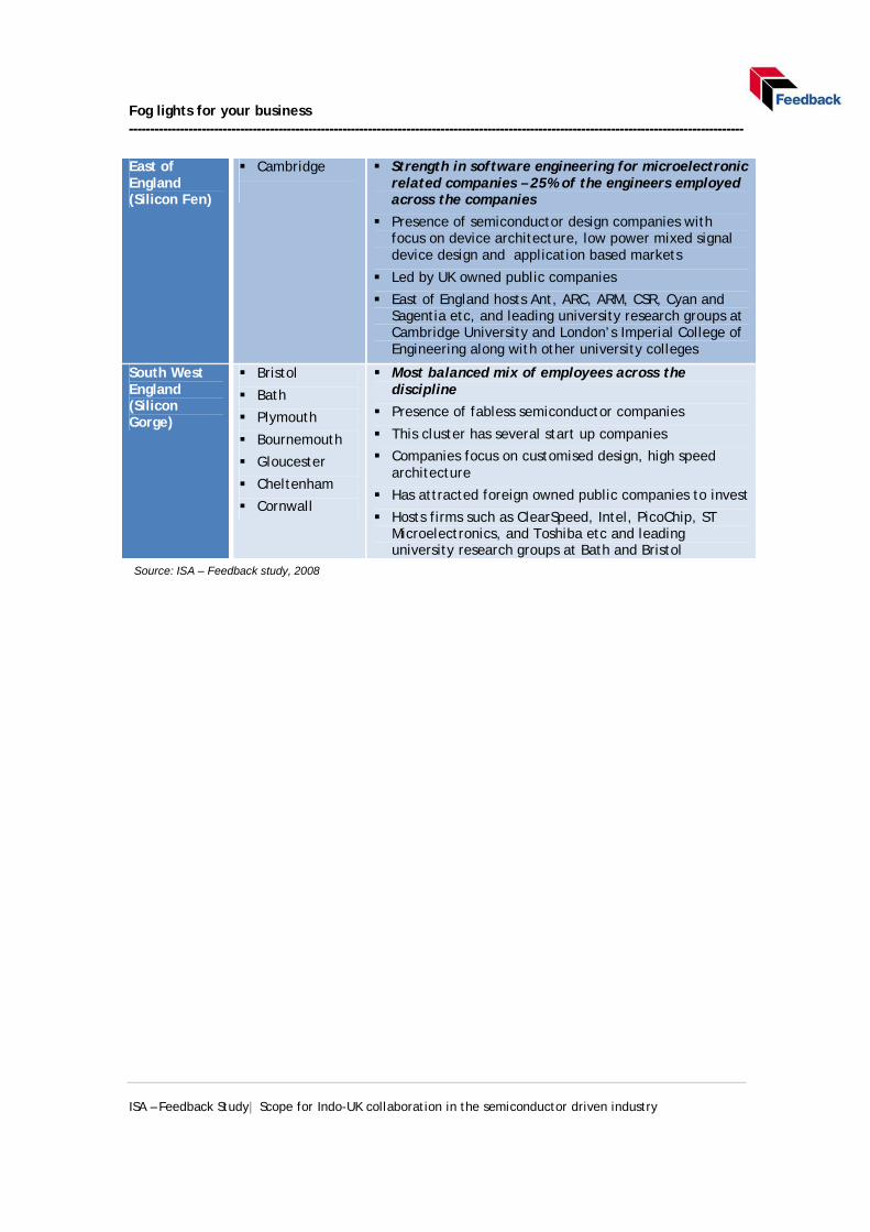
Fog lights for your business ------------------------------------------------------------------------------------------------------------------------------------------------
ISA – Feedback Study| Scope for Indo-UK collaboration in the semiconductor driven industry
East of England (Silicon Fen)
§ Cambridge
§ Strength in software engineering for microelectronic related companies – 25% of the engineers employed across the companies
§ Presence of semiconductor design companies with focus on device architecture, low power mixed signal device design and application based markets
§ Led by UK owned public companies
§ East of England hosts Ant, ARC, ARM, CSR, Cyan and Sagentia etc, and leading university research groups at Cambridge University and London’s Imperial College of Engineering along with other university colleges
South West England (Silicon Gorge)
§ Bristol
§ Bath
§ Plymouth
§ Bournemouth
§ Gloucester
§ Cheltenham
§ Cornwall
§ Most balanced mix of employees across the discipline
§ Presence of fabless semiconductor companies
§ This cluster has several start up companies
§ Companies focus on customised design, high speed architecture
§ Has attracted foreign owned public companies to invest
§ Hosts firms such as ClearSpeed, Intel, PicoChip, ST Microelectronics, and Toshiba etc and leading university research groups at Bath and Bristol
Source: ISA – Feedback study, 2008
Fog lights for your business ------------------------------------------------------------------------------------------------------------------------------------------------
ISA – Feedback Study| Scope for Indo-UK collaboration in the semiconductor driven industry
3.2 Universities in the UK – Overview 3.2.1 Overview There are nearly 100 universities in the UK which offer Electronics engineering undergraduate courses. Around 22,000 students in electronics related degree courses graduate out of these institutions annually. In addition to providing an excellent opportunity for companies to collaborate on research projects, industry sponsored post graduate courses allow technology driven companies to interact with this valuable source of well-qualified engineers. Around 27 universities in the UK focus on research in the field of semiconductors. Research in the UK is primarily led by academia along with a couple of doctorate (Ph D.) and post graduate students. A distinct feature in these universities is the presence of in-house fabrication labs. Almost all the large universities have in-house fabrication labs which support non – complex design for wafer fabrication. However, only a few are treated as commercial fabs for assisting the requirements of medium and small fabless companies in UK. Universities throughout the UK provide the basis of an extended research environment for electronics, and for semiconductor design in particular. There are more than 70 establishments involved in semiconductor design research projects, higher level education and training, or both. Practically all have strong mutually beneficial relationships with the industry in one form or another. Some universities have gained international recognition in certain areas, such as the University of Manchester with Professor Steve Furber’s work on asynchronous circuit design and Hilary Kahn’s contributions to CAD data formats for international standards (the Electronics Design Interchange Format). Imperial College London has an international reputation for work on field-programmable gate arrays (FPGA). Given the UK’s market strength in telecommunications, it is not surprising that more than 20 universities focus on electronics and communications technologies, some of these specialising in RF design. These include Aberdeen, Essex, Leeds, Newcastle and Sussex. System-on-Chip (SoC) design is offered as a subject by universities including Bristol, Edinburgh, Imperial College London, Lancaster, Manchester, Sheffield and Southampton. The Institute for System Level Integration in Livingston and Lancaster University have established a major UK resource in SoC test engineering. Meanwhile, high level language design (VHDL) is a focus at the universities of Surrey, Portsmouth and Napier. Digital signal processing is a particularly popular topic, covered by around 30 universities around the country. Collaboration with industry is important to UK universities, and some strong partnerships have been forged over many years. There are major joint ventures, such as Hitachi’s investment in the Cavendish Laboratory at the University of Cambridge. Long-term collaboration is prevalent, such as the work on high level and DSP design at the Queen’s University of Belfast, in collaboration with Amphion. There is also the project-based research, undertaken by postgraduates. NXP Semiconductors works very closely with the University of Southampton and Cardiff University, among others. Xilinx has a relationship with the universities of Hertfordshire and Strathclyde. ARM works closely with Liverpool and Sheffield universities. Toshiba has a joint venture in wireless telecom technology with the University of Bristol. Some of the leading universities for research in semiconductors include the Universities of Cambridge, Glasgow, Edinburgh, Manchester, Sheffield, Surrey, New Castle and Imperial College. Increasingly, universities are gearing up to meet the demand for continuous professional development, particularly in the engineering sector. A range of distance learning and modular courses are available for experienced engineers wanting to learn new skills and broaden their knowledge. The EPSRC (Engineering and Physical Sciences Research Council) funds these
Fog lights for your business ------------------------------------------------------------------------------------------------------------------------------------------------
ISA – Feedback Study| Scope for Indo-UK collaboration in the semiconductor driven industry
courses some of which cover VLSI design, DSP, RF design, SoC, VHDL to universities throughout the UK. Energy harvesting, which is a joint research project by the University of New Castle, Southampton and Manchester, along with Nano CMOS, a joint research project by University Glasgow, Manchester, Southampton and Edinburgh are the major university level projects currently being executed. 3.2.2 Nature of research University research in UK is driven by university professors. The focus has been on fundamental research (next generation device and material science) from basic silicon CMOS to silicon NANO electronics, Silicon Germanium and Galium Arsenide device fabrication and application oriented products. The research primarily targets market availability of application specific products in 2 – 3 years from the start of the research. Key research focus includes:
· Silicon device design · Device characterisation and modelling · New architecture development · Asynchronous design (low power, balancing power and frequency) · Network on chips · Photonic devices, integration of photons in Silicon layer · Semiconductor imaging · Special purpose RF chips and sensors

Fog lights for your business ------------------------------------------------------------------------------------------------------------------------------------------------
ISA – Feedback Study| Scope for Indo-UK collaboration in the semiconductor driven industry
Figure 23: Competency of select UK universities in design skills
Figure 24: Competency of select UK universities in application segments
3.2.3 Incubation centres
Source: ISA – Feedback study, 2008
Source: ISA – Feedback study, 2008
Fog lights for your business ------------------------------------------------------------------------------------------------------------------------------------------------
ISA – Feedback Study| Scope for Indo-UK collaboration in the semiconductor driven industry
Current status Incubation is a common practice in almost all the universities in the UK. Some universities like Cambridge, Manchester and Glasgow have spun out some of the best companies in the field of semiconductors, which are now planning to go global from their traditional UK / European operations. On an average, around 2-3 companies are spun out of the overall base of universities in UK in a year. Incubation in the UK has attracted a lot of venture capital funding for these start up companies, which primarily focus on semiconductor fabless design. Activities Incubation is a much sought after activity as the focus of research is application specific and towards commercial viability of products. The incubation period is typically 2 – 3 years wherein the research is funded by the EPSRC or the University board. The company gets access to state of the art infrastructure at the university campus. The highlight of the incubation is that once established, these companies return to the universities for research, thereby ensuring pay back to the universities. Outlook The active involvement of the government through funding, interest of venture capitalists to invest in start up companies and access to technology markets will be the drivers to increase the number of spin outs from these universities. The presence of science parks which are allied geographically to universities also provides an excellent environment for research spin offs and start up companies. 3.2.4 University - industry collaboration Current status University – industry collaboration is one of the most prominent features of semiconductor research activity in the UK. Around 50 – 60% of university research projects are done jointly with industries in some form or the other. Significant research focus is in the areas of RF design, System on Chip (SoC), VLSI, FPGA and DSP. Emphasis is placed on training the engineering graduates in new technology and system level design. Industrial sponsorships are encouraged, as all these courses have a significant project based element. The sponsors benefit significantly from the research resources available and attracting this new talent on a permanent basis. Operating model The companies approach universities for collaborative research in the field of semiconductors. The industries primarily seek design assistance, device modelling, performance analysis, new concept testing with universities. Over the years, large companies have invested in specific design and testing laboratories with the universities. Most often, companies fund the research activity and the research period is typically 8 months to 3 years depending upon the scope of research. The average project cost would range from £0.5 million to £4 million depending on the complexity of the project. Around 40 – 50% of the funds are supplied directly by companies in the form of fees, infrastructure set up and access to manufacturing set up. A research project typically involves 2 – 10 Research Fellows including academic staff as project lead and along with Doctorate and Masters’ students. In most of these collaboration activities, funding is offered to these students. Research grant of £25,000 for Masters and £75,000 for Ph D. students for a period of three years is typical.

Fog lights for your business ------------------------------------------------------------------------------------------------------------------------------------------------
ISA – Feedback Study| Scope for Indo-UK collaboration in the semiconductor driven industry
Table 13 depicts select examples of University - industry collaboration:
University Research areas Industry alliance
Sheffield · Development of imaging devices in the field of CMOS active pixel sensors for application segments like scientific and medical equipments
· Technology programme on active pixel sensors – based on CMOS technology and capable of expanding the traditional envelope of imaging capability with ultra-fast frame rates, flexible readout and integral intelligence
· Core expertise is in video coding technology, especially scalable video coding and compressed domain analysis for context-aware robust video delivery for applications ranging from low-resolution mobile devices to high-resolution display systems
· Automatic face recognition remains a strong activity, which has been recently augmented by work on shoeprint analysis and identification
· Kodak · Canon
Surrey · Focus in the field of device physics. Gallium Arsenide and Opto electronics are key research areas
· One of the leading universities in the UK for research in the field of Wireless and Satellite Communication devices. Has launched 20 odd satellites into the orbit. Currently developing integration of photonics in Silicon to increase optical sensitivity of materials. The various disciplines include:
§ Advanced Technology Institute – future electronic devices/integrated systems including nanoelectronics, nanobiotechnology and spintronics, high speed optoelectronics/ electronic devices, photonics, ion implantation research, large area electronics, modelling/ simulation of optoelectronic devices and polymer electronics
§ Centre for Communication Systems - Research – mobile cellular/ satellite communications, multimedia systems, communications networking
§ Centre for Vision, Speech and Signal Processing – image processing, pattern recognition, computer vision, biometrics, 3D broadcast, image/ video database retrieval, medical imaging, remote sensing
§ Centre for Nuclear and Radiation Physics – material characterisation over a wide range of II-VI and III-V semiconductors, using these materials for the development of novel semiconductor ionising radiation sensors
§ Computing – artificial intelligence, software and computer engineering, information
· Intel · Motorola

Fog lights for your business ------------------------------------------------------------------------------------------------------------------------------------------------
ISA – Feedback Study| Scope for Indo-UK collaboration in the semiconductor driven industry
systems § Mathematics – dynamical systems,
symmetry/patterns, numeric/computation, mathematical biology
§ Soft Condensed Matter Physics – conducting polymers/ nanocomposites, stimuli-responsive materials, nanotubes, novel NMR magnets
§ Surrey Space Centre – micro-mini satellite spacecraft engineering
New Castle § System design is the key research area § Current focus is in the space of asynchronous of
time, which focuses on low power and frequency distribution in circuits
§ Specialises in the field of design tools, device characterisation, system modelling, variability analysis, system on chip applications
§ Computing, smart card and security hardware segments are the other major application segments
§ The Microelectronics Research Group is known nationally and internationally for its expertise in two major knowledge areas:
• Microelectronics technology: strained Si/SiGe technology for high speed low power integrated circuits; SiC for high temperature high power electronics; reliability of IC interconnects; high-k dielectrics; fabrication; electrical and material characterisation; technology CAD; molecular electronics and carbon nanotubes. The group maintains class 100 clean rooms, together with extensive electrical and material characterisation facilities.
• Microelectronics system design: asynchronous system design; secure hardware design; synthesis and verification; metastability modelling and characterisation; synchroniser design; on-chip timing measurements; logarithmic scale processors; self test for SoC, concurrent error detection; design for testability and testing for high temperature SOI technologies.
· Intel · Atmel · Calixica · Pico Chip
Southampton § Southampton is one of the leading universities in the UK for research in the field of CMOS Technology
§ The School of Electronics and Computer Science at the University of Southampton is the largest of its kind in the UK; the department turns over around £ 23 million every year, over half of which is derived from collaborative research
§ The university focuses on Electronic systems and devices with specific focus on circuit designing, ultra low power systems, distribution computing, intelligent sensors and applications
§ Research interests encompass a wide spectrum of disciplines, covered by research groups - communications, declarative systems and software engineering, electronic systems design, image,
· NXP Semiconductors
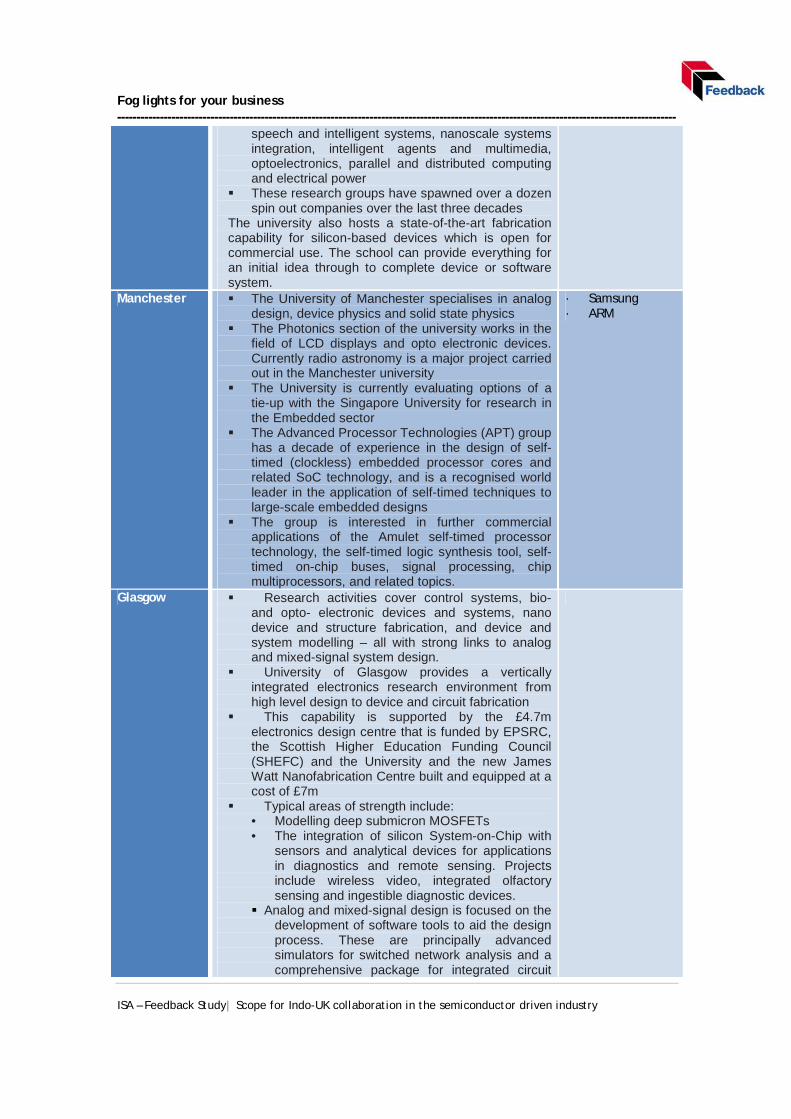
Fog lights for your business ------------------------------------------------------------------------------------------------------------------------------------------------
ISA – Feedback Study| Scope for Indo-UK collaboration in the semiconductor driven industry
speech and intelligent systems, nanoscale systems integration, intelligent agents and multimedia, optoelectronics, parallel and distributed computing and electrical power
§ These research groups have spawned over a dozen spin out companies over the last three decades
The university also hosts a state-of-the-art fabrication capability for silicon-based devices which is open for commercial use. The school can provide everything for an initial idea through to complete device or software system.
Manchester § The University of Manchester specialises in analog design, device physics and solid state physics
§ The Photonics section of the university works in the field of LCD displays and opto electronic devices. Currently radio astronomy is a major project carried out in the Manchester university
§ The University is currently evaluating options of a tie-up with the Singapore University for research in the Embedded sector
§ The Advanced Processor Technologies (APT) group has a decade of experience in the design of self-timed (clockless) embedded processor cores and related SoC technology, and is a recognised world leader in the application of self-timed techniques to large-scale embedded designs
§ The group is interested in further commercial applications of the Amulet self-timed processor technology, the self-timed logic synthesis tool, self-timed on-chip buses, signal processing, chip multiprocessors, and related topics.
· Samsung · ARM
Glasgow § Research activities cover control systems, bio- and opto- electronic devices and systems, nano device and structure fabrication, and device and system modelling – all with strong links to analog and mixed-signal system design.
§ University of Glasgow provides a vertically integrated electronics research environment from high level design to device and circuit fabrication
§ This capability is supported by the £4.7m electronics design centre that is funded by EPSRC, the Scottish Higher Education Funding Council (SHEFC) and the University and the new James Watt Nanofabrication Centre built and equipped at a cost of £7m
§ Typical areas of strength include: • Modelling deep submicron MOSFETs • The integration of silicon System-on-Chip with
sensors and analytical devices for applications in diagnostics and remote sensing. Projects include wireless video, integrated olfactory sensing and ingestible diagnostic devices.
§ Analog and mixed-signal design is focused on the development of software tools to aid the design process. These are principally advanced simulators for switched network analysis and a comprehensive package for integrated circuit
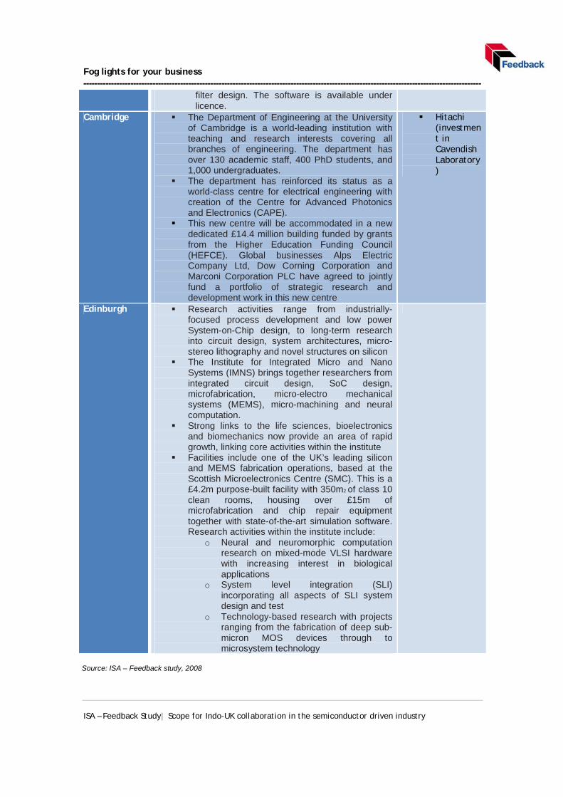
Fog lights for your business ------------------------------------------------------------------------------------------------------------------------------------------------
ISA – Feedback Study| Scope for Indo-UK collaboration in the semiconductor driven industry
filter design. The software is available under licence.
Cambridge § The Department of Engineering at the University of Cambridge is a world-leading institution with teaching and research interests covering all branches of engineering. The department has over 130 academic staff, 400 PhD students, and 1,000 undergraduates.
§ The department has reinforced its status as a world-class centre for electrical engineering with creation of the Centre for Advanced Photonics and Electronics (CAPE).
§ This new centre will be accommodated in a new dedicated £14.4 million building funded by grants from the Higher Education Funding Council (HEFCE). Global businesses Alps Electric Company Ltd, Dow Corning Corporation and Marconi Corporation PLC have agreed to jointly fund a portfolio of strategic research and development work in this new centre
§ Hitachi (investment in Cavendish Laboratory)
Edinburgh § Research activities range from industrially-focused process development and low power System-on-Chip design, to long-term research into circuit design, system architectures, micro-stereo lithography and novel structures on silicon
§ The Institute for Integrated Micro and Nano Systems (IMNS) brings together researchers from integrated circuit design, SoC design, microfabrication, micro-electro mechanical systems (MEMS), micro-machining and neural computation.
§ Strong links to the life sciences, bioelectronics and biomechanics now provide an area of rapid growth, linking core activities within the institute
§ Facilities include one of the UK’s leading silicon and MEMS fabrication operations, based at the Scottish Microelectronics Centre (SMC). This is a £4.2m purpose-built facility with 350m2 of class 10 clean rooms, housing over £15m of microfabrication and chip repair equipment together with state-of-the-art simulation software. Research activities within the institute include:
o Neural and neuromorphic computation research on mixed-mode VLSI hardware with increasing interest in biological applications
o System level integration (SLI) incorporating all aspects of SLI system design and test
o Technology-based research with projects ranging from the fabrication of deep sub-micron MOS devices through to microsystem technology
Source: ISA – Feedback study, 2008

Fog lights for your business ------------------------------------------------------------------------------------------------------------------------------------------------
ISA – Feedback Study| Scope for Indo-UK collaboration in the semiconductor driven industry
3.4 Venture Capitalists in UK – Overview Research activities in Semiconductors are funded by Engineering & Physical Sciences Research Council (EPSRC) – which is a Government funded body, and by industry and venture capitalists. Venture capitalists have been active in funding start up companies in the UK. UK has 30–40 venture capitalists active in the semiconductors segment funding both incubation centres as well as start-ups. A high proportion of venture capitalists exist in the Cambridge area. Fabless semiconductor companies are the most promising firms for venture capitalists at present. The active presence of venture capitalists in the UK is because of access to high technology driven European markets and high acceptance of designs by start-up firms. Technology focus and the ability to develop products suited to market requirements has been one of the major interest factors for venture capital investments in the UK. Key qualification criteria for venture capital investment
· Business plan for the company, road map for products and application markets · Current business need · Technology focus · Capabilities for delivering the product · Capabilities of the team executing the venture · Market opportunity
Activities Some of the reputed venture capitalists include Schroder Ventures, 3i, Amadeus, Forward Innovation Fund, Pond Venture Partner Limited, Atlas Venture, Highland Capital Partners, Scottish Equity Partners and Merchant Ventures. These venture capitalists typically adopt two levels of funding:
· Seed funding: Funding during the initial scope of project, typically when the time taken from design to getting the layout for the execution team. The average amount would range from £0.3 to 0.5 million
· Prototype funding: This type of funding is during the product development phase. Ideally the period is from design to first product development stage. The average amount would range from £2 to 10 million depending upon the complexity of the project.
The most challenging aspect for venture capitalists is in taking the prototype to the market and awaiting its success. Bulk of the investment is during this phase of the business. Once the company starts picking up pace in the market when the products and the technology are accepted, the venture capitalists fund the company every two years depending on the growth plan and market reach. Outlook The outlook for venture capitalist funding completely depends on the market attractiveness of the products and technology focus in the near future. There has been increasing focus and interest shown by venture capitalists to assist semiconductor research groups in the UK.
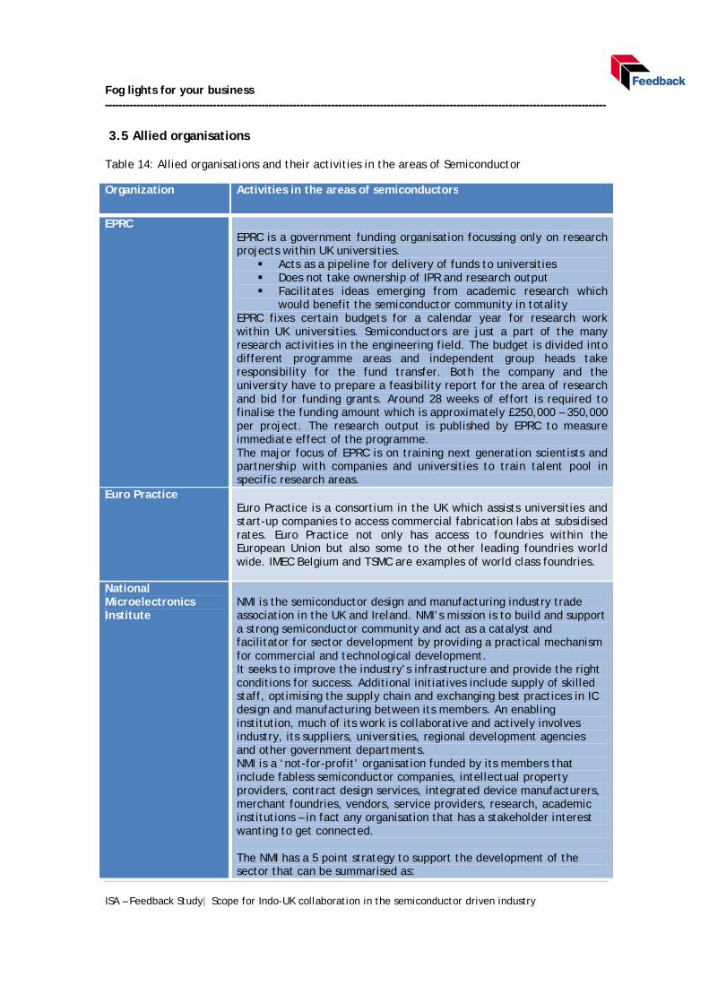
Fog lights for your business ------------------------------------------------------------------------------------------------------------------------------------------------
ISA – Feedback Study| Scope for Indo-UK collaboration in the semiconductor driven industry
3.5 Allied organisations Table 14: Allied organisations and their activities in the areas of Semiconductor
Organization Activities in the areas of semiconductors
EPRC EPRC is a government funding organisation focussing only on research projects within UK universities.
§ Acts as a pipeline for delivery of funds to universities § Does not take ownership of IPR and research output § Facilitates ideas emerging from academic research which
would benefit the semiconductor community in totality EPRC fixes certain budgets for a calendar year for research work within UK universities. Semiconductors are just a part of the many research activities in the engineering field. The budget is divided into different programme areas and independent group heads take responsibility for the fund transfer. Both the company and the university have to prepare a feasibility report for the area of research and bid for funding grants. Around 28 weeks of effort is required to finalise the funding amount which is approximately £250,000 – 350,000 per project. The research output is published by EPRC to measure immediate effect of the programme. The major focus of EPRC is on training next generation scientists and partnership with companies and universities to train talent pool in specific research areas.
Euro Practice Euro Practice is a consortium in the UK which assists universities and start-up companies to access commercial fabrication labs at subsidised rates. Euro Practice not only has access to foundries within the European Union but also some to the other leading foundries world wide. IMEC Belgium and TSMC are examples of world class foundries.
National Microelectronics Institute
NMI is the semiconductor design and manufacturing industry trade association in the UK and Ireland. NMI’s mission is to build and support a strong semiconductor community and act as a catalyst and facilitator for sector development by providing a practical mechanism for commercial and technological development. It seeks to improve the industry’s infrastructure and provide the right conditions for success. Additional initiatives include supply of skilled staff, optimising the supply chain and exchanging best practices in IC design and manufacturing between its members. An enabling institution, much of its work is collaborative and actively involves industry, its suppliers, universities, regional development agencies and other government departments. NMI is a ‘not-for-profit’ organisation funded by its members that include fabless semiconductor companies, intellectual property providers, contract design services, integrated device manufacturers, merchant foundries, vendors, service providers, research, academic institutions – in fact any organisation that has a stakeholder interest wanting to get connected. The NMI has a 5 point strategy to support the development of the sector that can be summarised as:
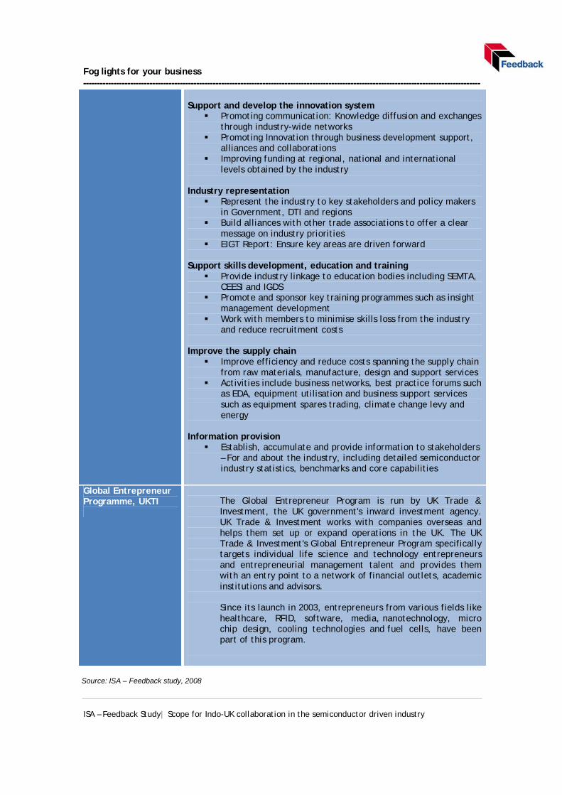
Fog lights for your business ------------------------------------------------------------------------------------------------------------------------------------------------
ISA – Feedback Study| Scope for Indo-UK collaboration in the semiconductor driven industry
Support and develop the innovation system
§ Promoting communication: Knowledge diffusion and exchanges through industry-wide networks
§ Promoting Innovation through business development support, alliances and collaborations
§ Improving funding at regional, national and international levels obtained by the industry
Industry representation
§ Represent the industry to key stakeholders and policy makers in Government, DTI and regions
§ Build alliances with other trade associations to offer a clear message on industry priorities
§ EIGT Report: Ensure key areas are driven forward Support skills development, education and training
§ Provide industry linkage to education bodies including SEMTA, CEESI and IGDS
§ Promote and sponsor key training programmes such as insight management development
§ Work with members to minimise skills loss from the industry and reduce recruitment costs
Improve the supply chain
§ Improve efficiency and reduce costs spanning the supply chain from raw materials, manufacture, design and support services
§ Activities include business networks, best practice forums such as EDA, equipment utilisation and business support services such as equipment spares trading, climate change levy and energy
Information provision
§ Establish, accumulate and provide information to stakeholders – For and about the industry, including detailed semiconductor industry statistics, benchmarks and core capabilities
Global Entrepreneur Programme, UKTI
The Global Entrepreneur Program is run by UK Trade & Investment, the UK government's inward investment agency. UK Trade & Investment works with companies overseas and helps them set up or expand operations in the UK. The UK Trade & Investment's Global Entrepreneur Program specifically targets individual life science and technology entrepreneurs and entrepreneurial management talent and provides them with an entry point to a network of financial outlets, academic institutions and advisors. Since its launch in 2003, entrepreneurs from various fields like healthcare, RFID, software, media, nanotechnology, micro chip design, cooling technologies and fuel cells, have been part of this program.
Source: ISA – Feedback study, 2008

Fog lights for your business ------------------------------------------------------------------------------------------------------------------------------------------------
ISA – Feedback Study| Scope for Indo-UK collaboration in the semiconductor driven industry
3.6 Analysis of the UK semiconductor industry
3.6.1 Strengths and weaknesses of UK universities in the field of semiconductors: Figure25: Depicts the level of semiconductor activities in the UK universities
Table 15: Definitions Table 15: Definitions
Categories Variables Description Research activity
VLSI design Activities in the field of VLSI, FPGA design Process related research Research carried out on device physics - alternative
materials, characterization Fundamental research Research activity on futuristic technology EDA Modelling and simulation of devices, system Application based research Research on direct end products
Infrastructure and resources
Infrastructure Presence of labs and availability of kits for research activities
Source of funds Funds generated through university accruals, government, companies collaborated for research
Incubation Activities of incubation cell within universities and number of start up (spun out of the system) companies
Talent pool Number of students pursuing semiconductor research in universities
Research initiative
University driven research Research initiated by university professors Company driven research Research initiated by companies for assistance
through universities
0 1 2 3 4 5 6 7 8 9 10
EDA
Application based research
Process related research
VLSI design
Talent pool
Source of funds
Company driven research
Fundamental research
University driven research
Incubation
Infrastructure
Extent of semiconductor research activities and support from companies and funding
funding
Research initiative Infrastructure and Resources
Research Activities
High Low
Source: ISA – Feedback study, 2008
Source: ISA – Feedback study, 2008
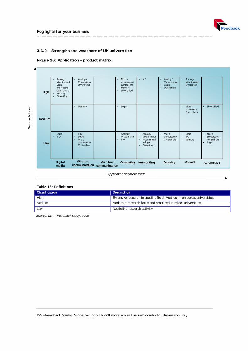
Fog lights for your business ------------------------------------------------------------------------------------------------------------------------------------------------
ISA – Feedback Study| Scope for Indo-UK collaboration in the semiconductor driven industry
3.6.2 Strengths and weakness of UK universities Figure 26: Application – product matrix
Table 16: Definitions
Classification Description
High Extensive research in specific field. Most common across universities.
Medium Moderate research focus and practiced in select universities.
Low Negligible research activity
• Micro-processors / Controllers
• Logic
• Logic • I/O • Memory
• Micro-processors / Controllers
• Analog / Mixed signal
• Programmable logic
• Diversified
• Analog / Mixed signal
• I/O
• I/O • Logic • Micro-
processors / Controllers
• Logic • I/O
• Diversified
• Micro-
processors / Controllers
• Logic
• Memory
• Analog /
Mixed signal • Diversified
• Analog / Mixed signal
• Logic • Diversified
• I/O
• Micro-
processors / Controllers
• Memory • Diversified
• Analog /
Mixed signal • Diversified
• Analog / Mixed signal
• Micro-processors / Controllers
• Memory • Diversified
High
Medium
Low
Digital media
Wireless communication
Wire line communication
Computing Networking Security Medical Automotive
Res
earc
h fo
cus
Application segment focus
Source: ISA – Feedback study, 2008
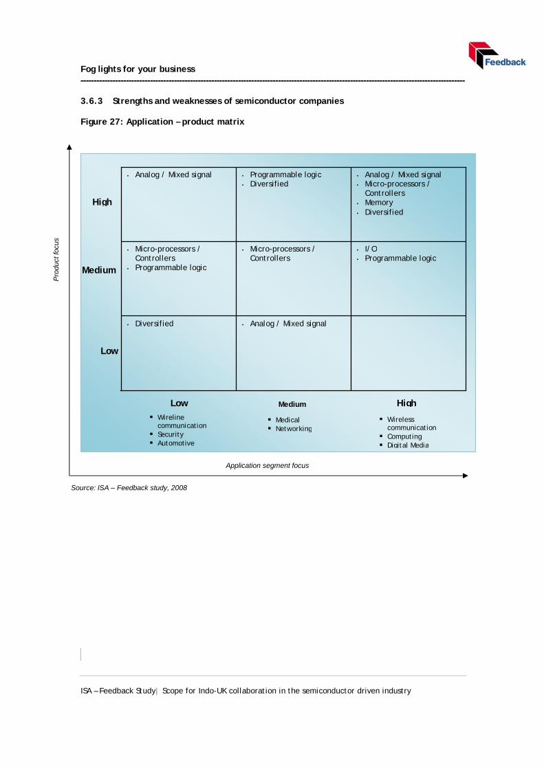
Fog lights for your business ------------------------------------------------------------------------------------------------------------------------------------------------
ISA – Feedback Study| Scope for Indo-UK collaboration in the semiconductor driven industry
3.6.3 Strengths and weaknesses of semiconductor companies Figure 27: Application – product matrix
• Analog / Mixed signal
• Diversified
• I/O • Programmable logic
• Micro-processors / Controllers
• Micro-processors / Controllers
• Programmable logic
• Analog / Mixed signal • Micro-processors /
Controllers • Memory • Diversified
• Programmable logic • Diversified
• Analog / Mixed signal
High
Low
High Medium Low § Wireline
communication § Security § Automotive
§ Medical § Networking
§ Wireless communication
§ Computing § Digital Media
Application segment focus
Medium
Source: ISA – Feedback study, 2008
Pro
duct
focu
s