scipp r&d on time-over- threshold electronics and long
TRANSCRIPT
SCIPP R&D on Time-Over-
Threshold Electronics and Long-
Ladder Readout
6th SiLC Meeting Torino, Italy
December 17, 2007
Bruce Schumm
Santa Cruz Institute for Particle Physics
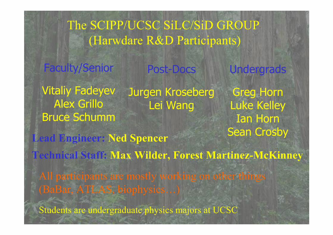
Faculty/Senior
Vitaliy FadeyevAlex Grillo
Bruce Schumm
Post-Docs
Jurgen KrosebergLei Wang
Undergrads
Greg HornLuke KelleyIan Horn
Sean Crosby
The SCIPP/UCSC SiLC/SiD GROUP
(Harwdare R&D Participants)
Lead Engineer: Ned Spencer
Technical Staff: Max Wilder, Forest Martinez-McKinney
All participants are mostly working on other things
(BaBar, ATLAS, biophysics…)
Students are undergraduate physics majors at UCSC
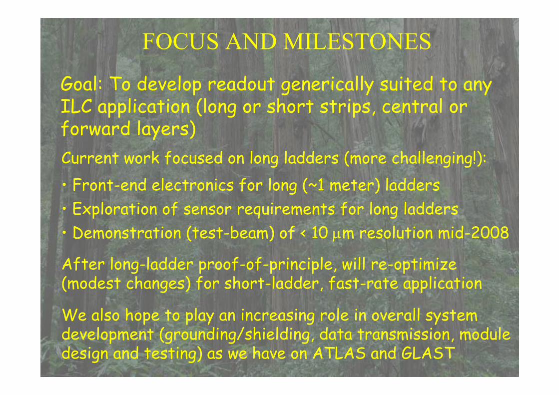
FOCUS AND MILESTONES
Goal: To develop readout generically suited to any ILC application (long or short strips, central or forward layers)
Current work focused on long ladders (more challenging!):
• Front-end electronics for long (~1 meter) ladders
• Exploration of sensor requirements for long ladders
• Demonstration (test-beam) of < 10 µm resolution mid-2008
After long-ladder proof-of-principle, will re-optimize (modest changes) for short-ladder, fast-rate application
We also hope to play an increasing role in overall system development (grounding/shielding, data transmission, module design and testing) as we have on ATLAS and GLAST

BRIEF SUMMARY OF STATUS
Testing of 8-channel (LSTFE-1) prototype fairly advanced:
•Reproducible operation (4 operating boards)
•Most features working, with needed refinements understood
•A number of “subtleties” (e.g. channel matching, environmental sensitivity) under control
•Starting to make progress on fundamental issues confronting long-ladder/high-resolution limit.
Design of 128-channel prototype (LSTFE-2) well underway (July submission)
Now for the details…
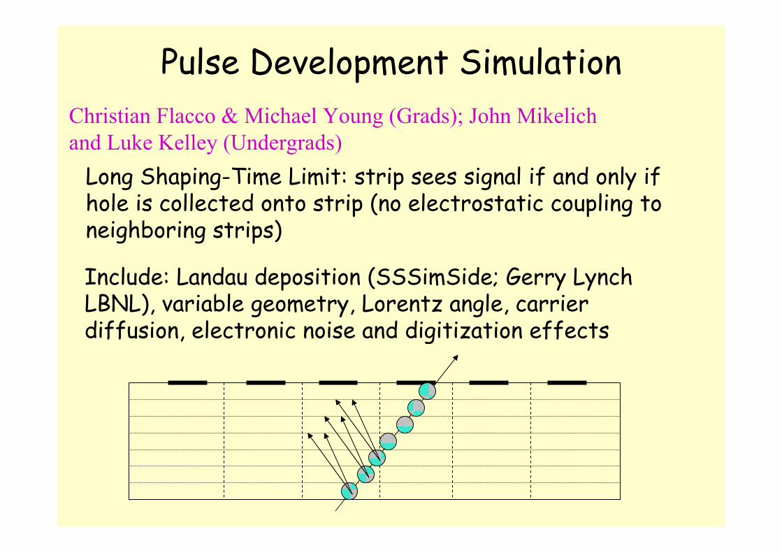
Pulse Development Simulation
Long Shaping-Time Limit: strip sees signal if and only if hole is collected onto strip (no electrostatic coupling to neighboring strips)
Include: Landau deposition (SSSimSide; Gerry Lynch LBNL), variable geometry, Lorentz angle, carrier diffusion, electronic noise and digitization effects
Christian Flacco & Michael Young (Grads); John Mikelich
and Luke Kelley (Undergrads)
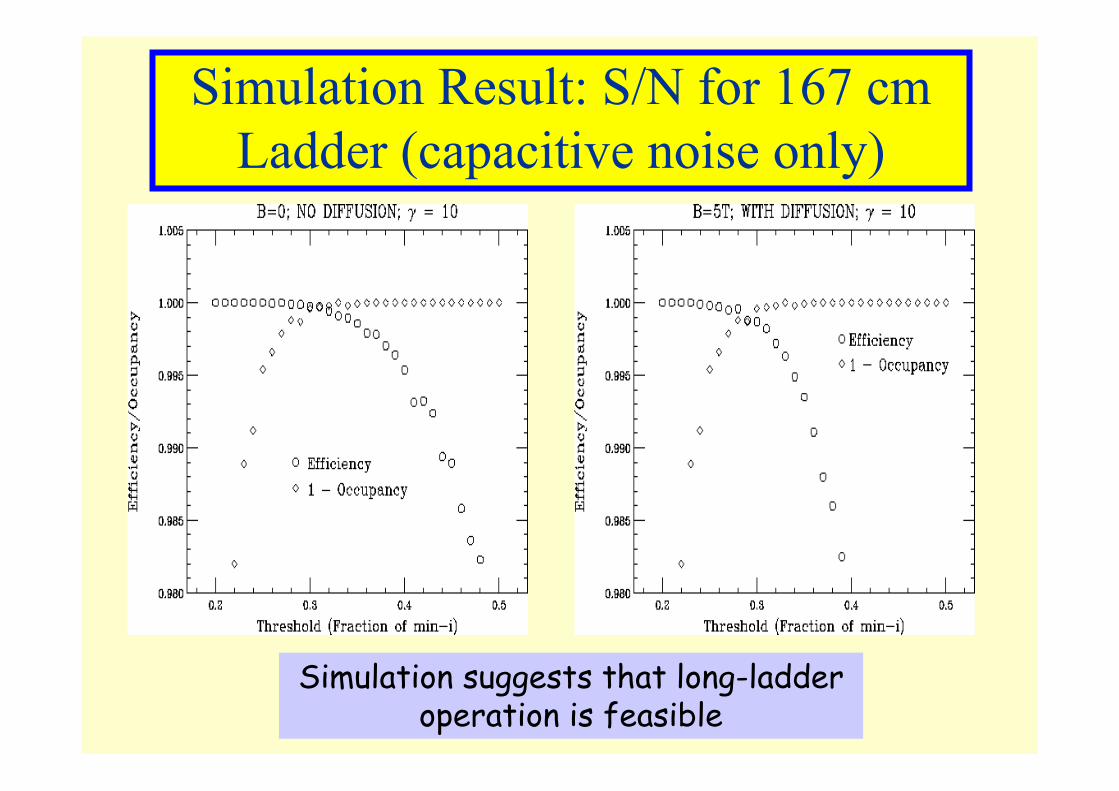
Simulation Result: S/N for 167 cm
Ladder (capacitive noise only)
Simulation suggests that long-ladder operation is feasible
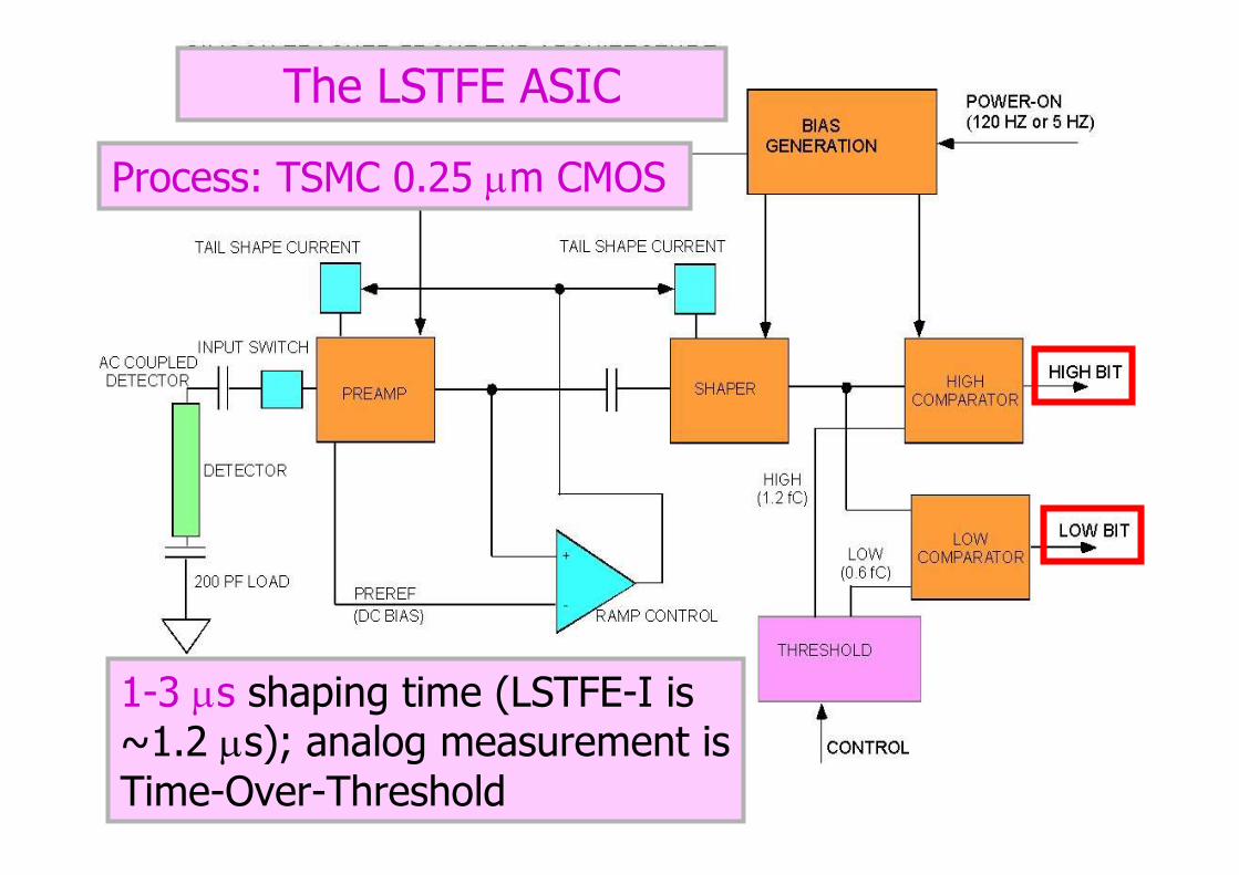
1-3 µs shaping time (LSTFE-I is ~1.2 µs); analog measurement is Time-Over-Threshold
Process: TSMC 0.25 µm CMOS
The LSTFE ASIC

1/4 mip
1 mip
128 mip
Operating point threshold
Readout threshold
High gain advantageous
for overall performance
(channel matching)

Electronics Simulation: Resolution
Detector Noise:
Capacitive contribution; from SPICE simulation normalized to bench tests with GLAST electronics
Analog Measurement:
Provided by time-over-threshold; lookup table provides conversions back into analog pulse height (as for actual data)
RMS
Gaussian Fit
Detector Resolution (units of 10µm)
Lower (read) threshold in fraction of min-i
(High threshold is at 0.29 times min-i)
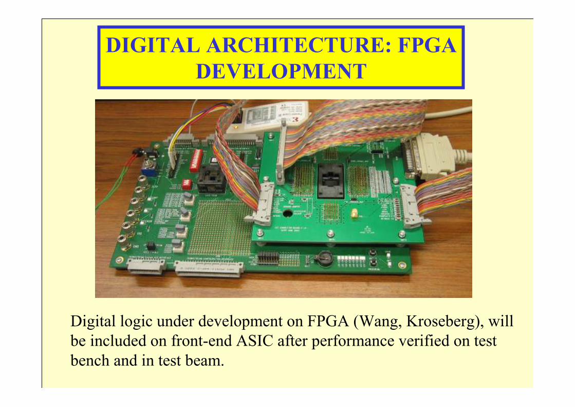
DIGITAL ARCHITECTURE: FPGA
DEVELOPMENT
Digital logic under development on FPGA (Wang, Kroseberg), will
be included on front-end ASIC after performance verified on test
bench and in test beam.
FIF
O (L
eadin
g and
trailin
g tra
nsitio
ns)
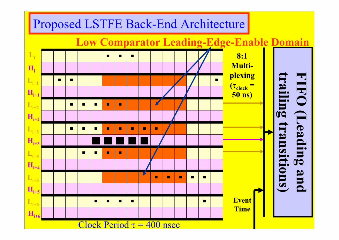
Low Comparator Leading-Edge-Enable DomainLi
Hi
Hi+4
Hi+1
Hi+2
Hi+3
Hi+5
Hi+6
Li+1
Li+2
Li+3
Li+4
Li+5
Li+6
Proposed LSTFE Back-End Architecture
Clock Period τ = 400 nsec
Event
Time
8:1
Multi-
plexing
(ττττclock =
50 ns)
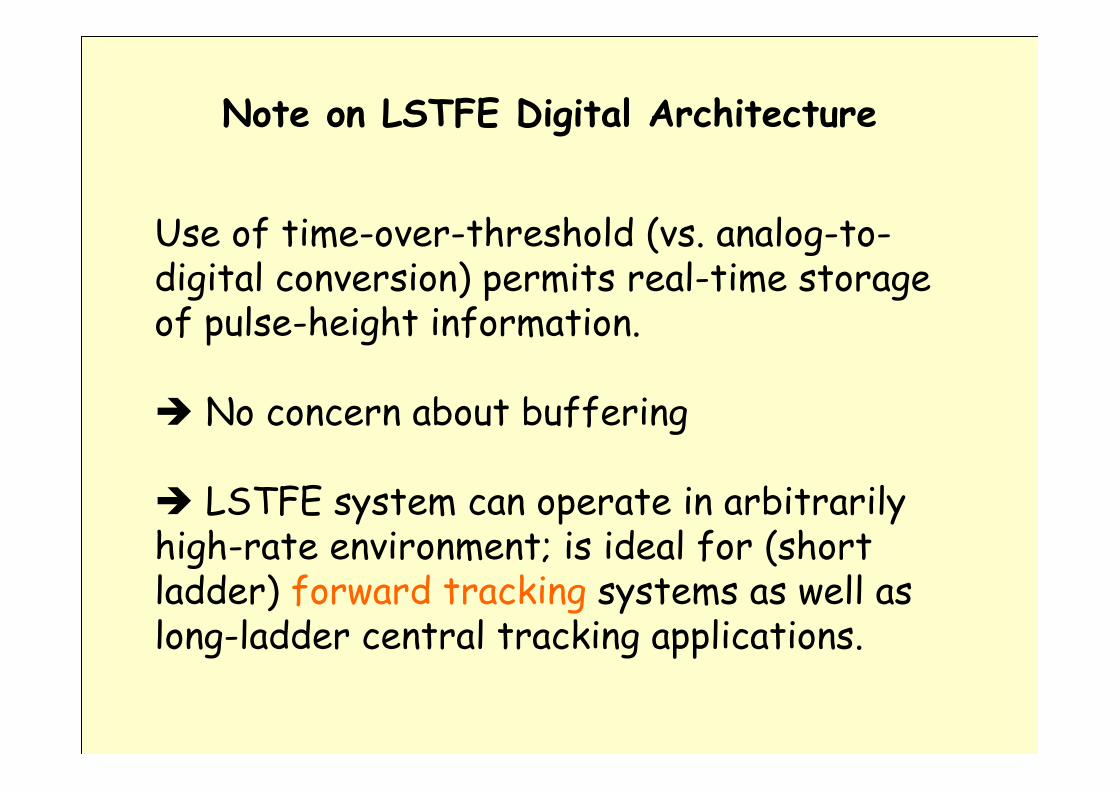
Note on LSTFE Digital Architecture
Use of time-over-threshold (vs. analog-to-digital conversion) permits real-time storage of pulse-height information.
No concern about buffering
LSTFE system can operate in arbitrarily high-rate environment; is ideal for (short ladder) forward tracking systems as well as long-ladder central tracking applications.
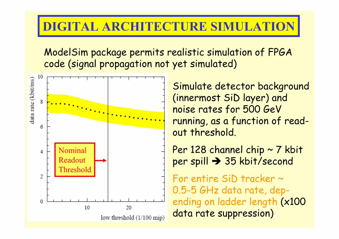
DIGITAL ARCHITECTURE SIMULATION
ModelSim package permits realistic simulation of FPGA code (signal propagation not yet simulated)
Simulate detector background (innermost SiD layer) and noise rates for 500 GeVrunning, as a function of read-out threshold.
Per 128 channel chip ~ 7 kbitper spill 35 kbit/second
For entire SiD tracker ~ 0.5-5 GHz data rate, dep-ending on ladder length (x100 data rate suppression)
Nominal
Readout
Threshold
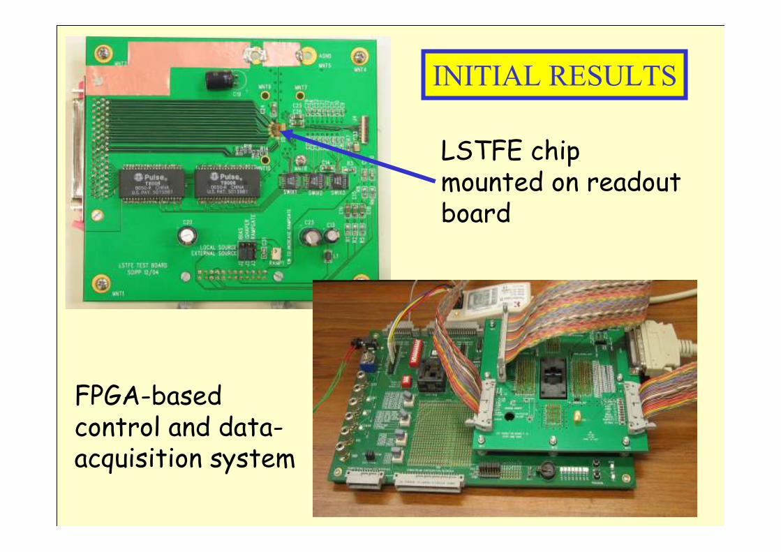
FPGA-based control and data-acquisition system
INITIAL RESULTS
LSTFE chip mounted on readout board
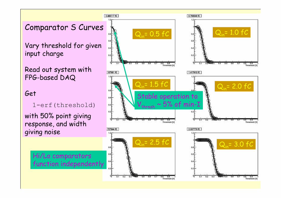
Comparator S Curves
Vary threshold for given input charge
Read out system with FPG-based DAQ
Get
1-erf(threshold)
with 50% point giving response, and width giving noise
Stable operation toVthresh ~ 5% of min-I
Qin= 0.5 fC
Qin= 3.0 fCQin= 2.5 fC
Qin= 2.0 fCQin= 1.5 fC
Qin= 1.0 fC
Hi/Lo comparators function independently
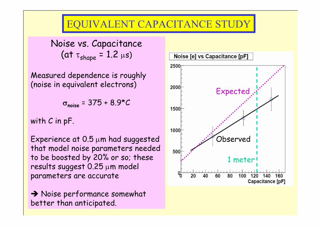
Noise vs. Capacitance (at τshape = 1.2 µs)
Measured dependence is roughly(noise in equivalent electrons)
σσσσnoise = 375 + 8.9*C
with C in pF.
Experience at 0.5 µm had suggested that model noise parameters needed to be boosted by 20% or so; these results suggest 0.25 µm model parameters are accurate
Noise performance somewhat better than anticipated.
Observed
Expected
1 meter
EQUIVALENT CAPACITANCE STUDY
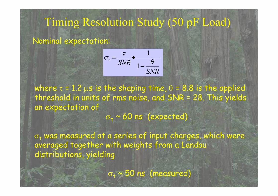
Timing Resolution Study (50 pF Load)
Nominal expectation:
SNR
SNRt θ
τσ
−
•=
1
1
where τ = 1.2 µs is the shaping time, θ = 8.8 is the applied threshold in units of rms noise, and SNR = 28. This yields an expectation of
σt ~ 60 ns (expected)
σt was measured at a series of input charges, which were averaged together with weights from a Landau distributions, yielding
σt ~ 50 ns (measured)
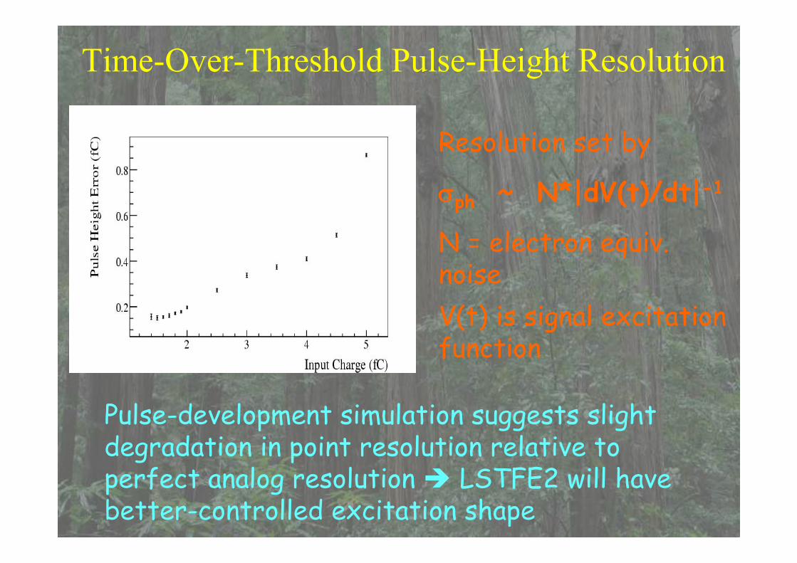
Time-Over-Threshold Pulse-Height Resolution
Resolution set by
σσσσph ~ N*|dV(t)/dt|-1
N = electron equiv. noise
V(t) is signal excitation function
Pulse-development simulation suggests slight degradation in point resolution relative to perfect analog resolution LSTFE2 will have better-controlled excitation shape
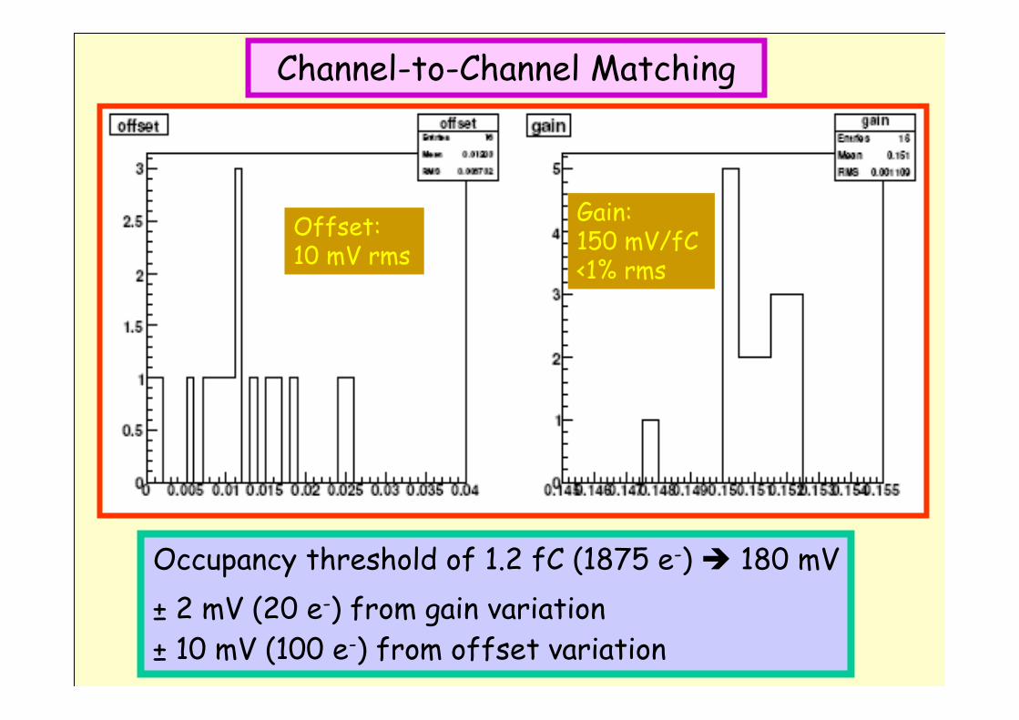
Channel-to-Channel Matching
Offset: 10 mV rms
Gain: 150 mV/fC <1% rms
Occupancy threshold of 1.2 fC (1875 e-) 180 mV
± 2 mV (20 e-) from gain variation
± 10 mV (100 e-) from offset variation
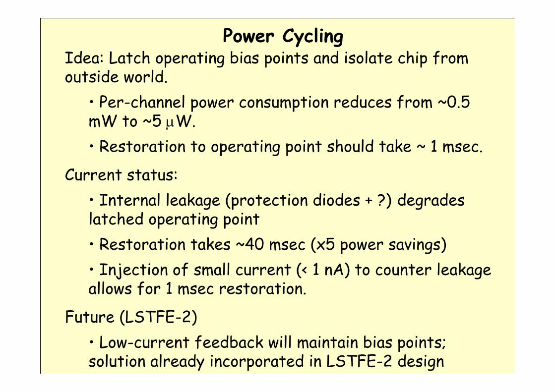
Power CyclingIdea: Latch operating bias points and isolate chip from outside world.
• Per-channel power consumption reduces from ~0.5 mW to ~5 µW.
• Restoration to operating point should take ~ 1 msec.
Current status:
• Internal leakage (protection diodes + ?) degrades latched operating point
• Restoration takes ~40 msec (x5 power savings)
• Injection of small current (< 1 nA) to counter leakage allows for 1 msec restoration.
Future (LSTFE-2)
• Low-current feedback will maintain bias points; solution already incorporated in LSTFE-2 design

Preamp Response
Power Control
Shaper Response
Power Cycling with Small Injected Current
Solution in hand to maintain bias levels in “off” state with low-power feedback; will eliminate need for external trickle current

LONG LADDER CONSTRUCTION
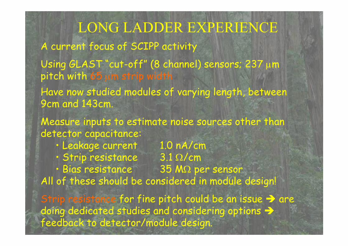
LONG LADDER EXPERIENCE
A current focus of SCIPP activity
Using GLAST “cut-off” (8 channel) sensors; 237 µm pitch with 65 µm strip width
Have now studied modules of varying length, between 9cm and 143cm.
Measure inputs to estimate noise sources other than detector capacitance:
• Leakage current 1.0 nA/cm• Strip resistance 3.1 Ω/cm• Bias resistance 35 MΩ per sensor
All of these should be considered in module design!
Strip resistance for fine pitch could be an issue aredoing dedicated studies and considering options feedback to detector/module design.
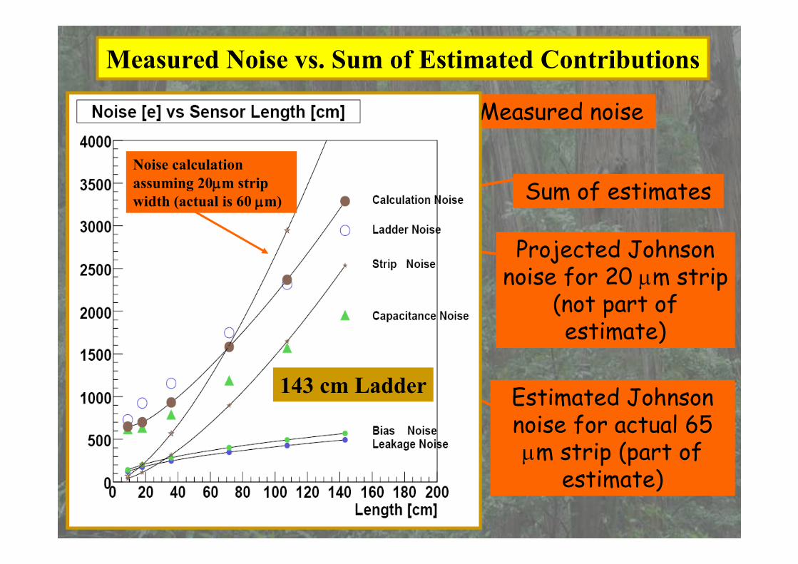
Measured Noise vs. Sum of Estimated Contributions
72 cm Ladder
Estimated Johnson noise for actual 65 µm strip (part of
estimate)
Projected Johnson noise for 20 µm strip
(not part of estimate)
Measured noise
Sum of estimates
143 cm Ladder
Noise calculation
assuming 20µµµµm strip
width (actual is 60 µµµµm)
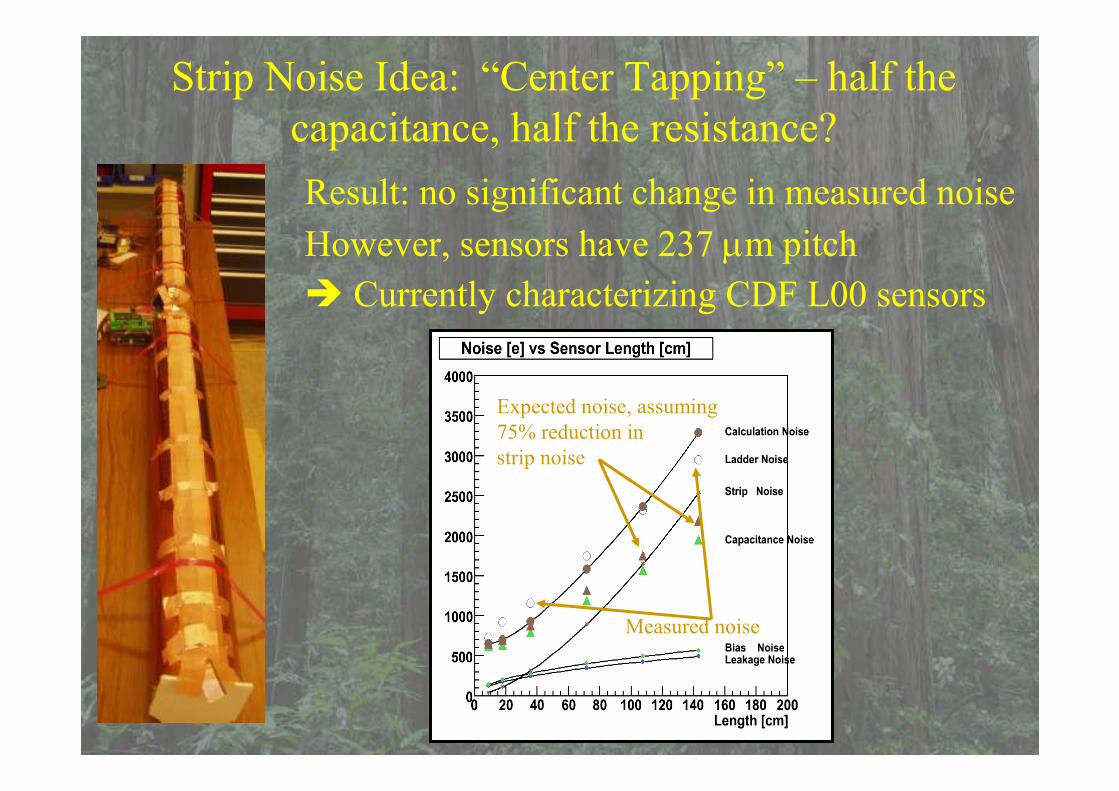
Strip Noise Idea: “Center Tapping” – half the
capacitance, half the resistance?
Result: no significant change in measured noise
However, sensors have 237 µm pitch
Currently characterizing CDF L00 sensors
Measured noise
Expected noise, assuming
75% reduction in
strip noise

TIME-OVER-THRESHOLD READOUT SUMMARY
The LSTFE readout system is:
• Universally applicable (long strips, short strips, central, forward, SiD, LDC, GLD, 4th…)
• Rigorously optimized for ILC tracking
• Relative simple (reliability, yield)
• In a relatively advanced stage of development
• Is now being used as an instrument to understand fundamental principles of long ladder operation, particularly for narrow strips (CDF Layer00 sensors available, being qualified)
RANDOM BACK-UP
SLIDES
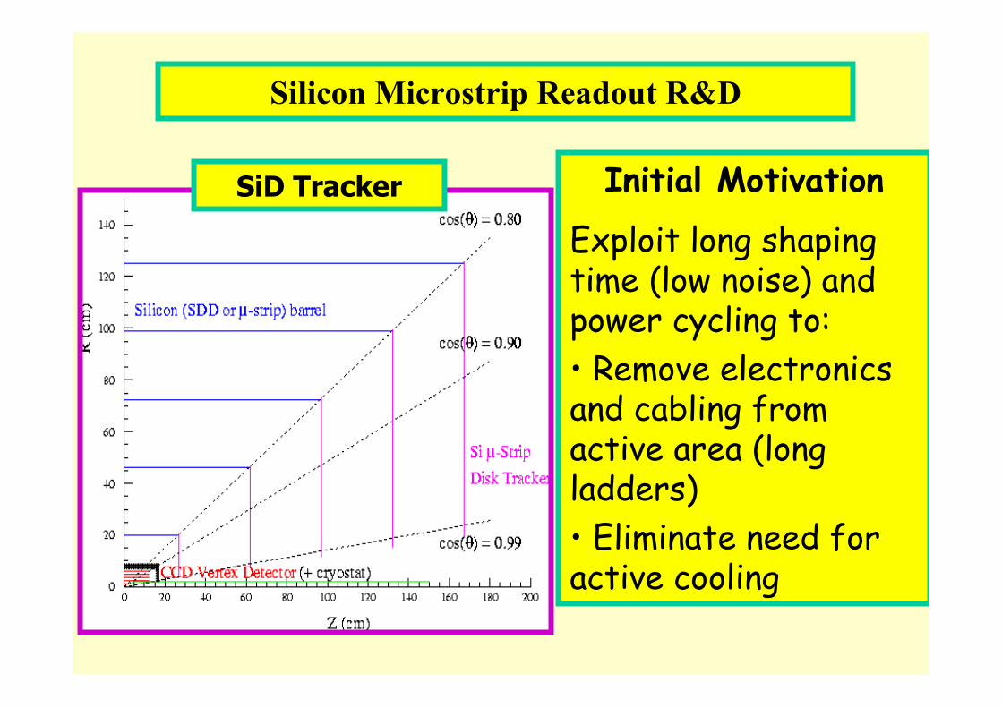
Silicon Microstrip Readout R&D
Initial Motivation
Exploit long shaping time (low noise) and power cycling to:
• Remove electronics and cabling from active area (long ladders)
• Eliminate need for active cooling
SiD Tracker
c
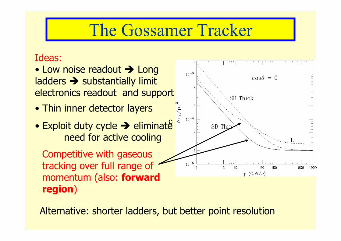
The Gossamer Tracker
Ideas:• Low noise readout Long ladders substantially limit electronics readout and support
• Thin inner detector layers
• Exploit duty cycle eliminate need for active cooling
Competitive with gaseous tracking over full range of momentum (also: forward region)
Alternative: shorter ladders, but better point resolution

Alternative: shorter ladders, but better point resolution
The LSTFE approach would be well suited to use in short-strip applications, and would offer several potential advantages relative to other approaches
• Optimized for LC tracking (less complex)
• More efficient data flow
• No need for buffering
Would require development of2000 channel chip w/ bump bonding (should be solved by KPiX development)
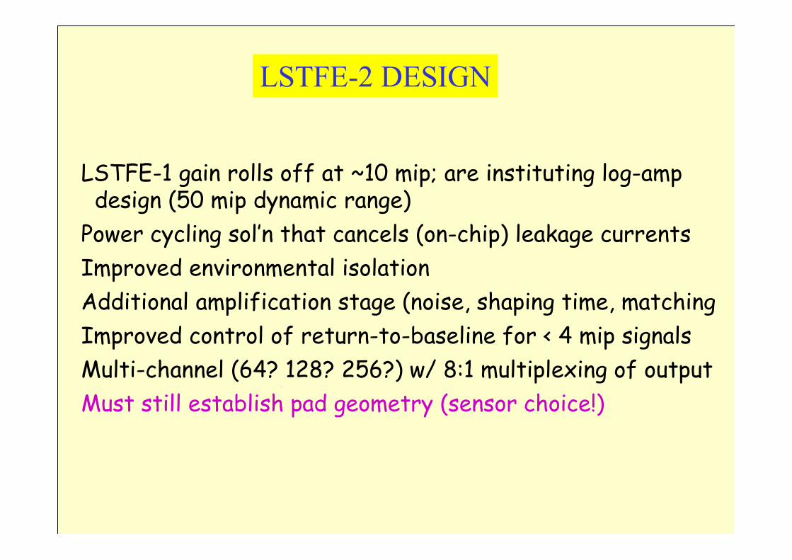
LSTFE-2 DESIGN
LSTFE-1 gain rolls off at ~10 mip; are instituting log-ampdesign (50 mip dynamic range)
Power cycling sol’n that cancels (on-chip) leakage currents
Improved environmental isolation
Additional amplification stage (noise, shaping time, matching
Improved control of return-to-baseline for < 4 mip signals
Multi-channel (64? 128? 256?) w/ 8:1 multiplexing of output
Must still establish pad geometry (sensor choice!)
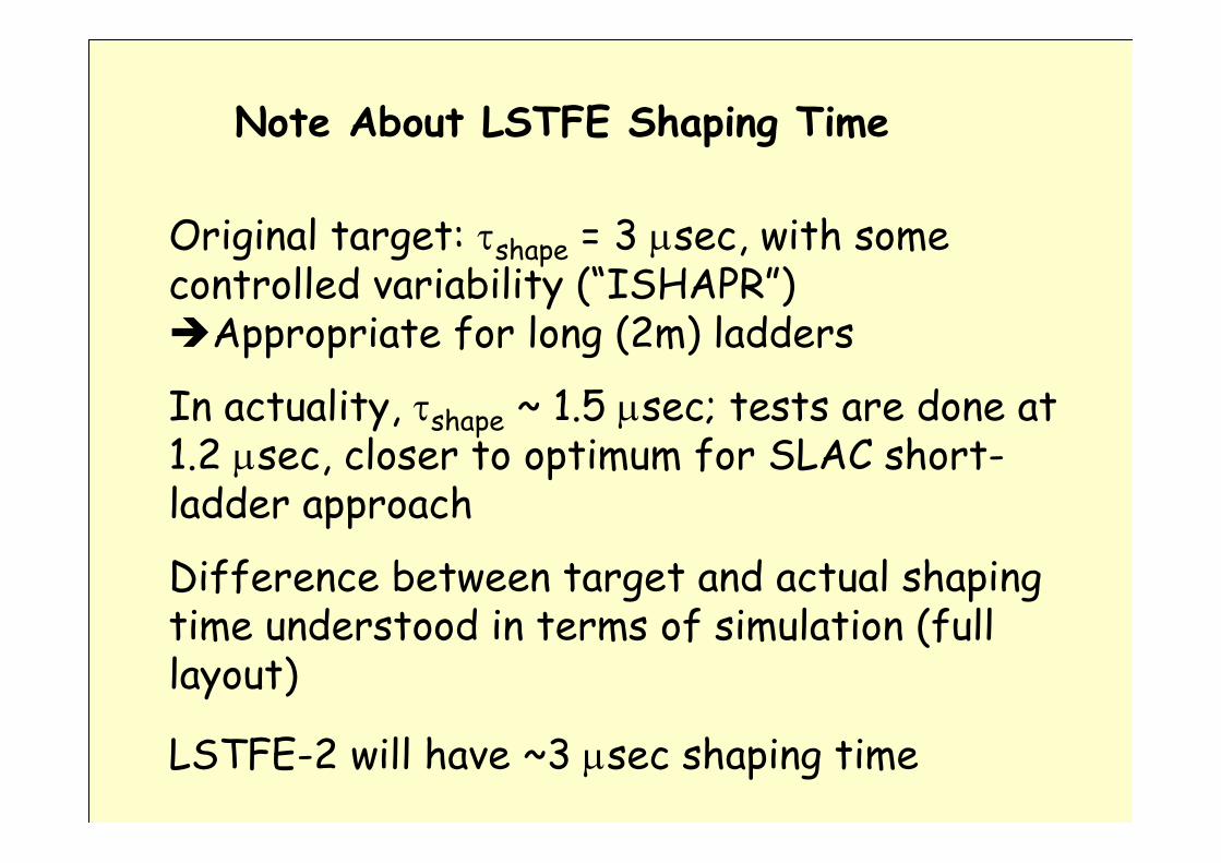
Note About LSTFE Shaping Time
Original target: τshape = 3 µsec, with some controlled variability (“ISHAPR”)Appropriate for long (2m) ladders
In actuality, τshape ~ 1.5 µsec; tests are done at 1.2 µsec, closer to optimum for SLAC short-ladder approach
Difference between target and actual shaping time understood in terms of simulation (full layout)
LSTFE-2 will have ~3 µsec shaping time