saa7104h; saa7105h digital video encoder · saa7104h; saa7105h digital video encoder. 2004 mar 04 2...
TRANSCRIPT
DATA SHEET
Product specification 2004 Mar 04
INTEGRATED CIRCUITS
SAA7104H; SAA7105HDigital video encoder
Philips Semiconductors Product specification
Digital video encoder SAA7104H; SAA7105H
CONTENTS
1 FEATURES
2 GENERAL DESCRIPTION
3 QUICK REFERENCE DATA
4 ORDERING INFORMATION
5 BLOCK DIAGRAM
6 PINNING
7 FUNCTIONAL DESCRIPTION
7.1 Reset conditions7.2 Input formatter7.3 RGB LUT7.4 Cursor insertion7.5 RGB Y-CB-CR matrix7.6 Horizontal scaler7.7 Vertical scaler and anti-flicker filter7.8 FIFO7.9 Border generator7.10 Oscillator and Discrete Time Oscillator (DTO)7.11 Low-pass Clock Generation Circuit (CGC)7.12 Encoder7.13 RGB processor7.14 Triple DAC7.15 HD data path7.16 Timing generator7.17 Pattern generator for HD sync pulses7.18 I2C-bus interface7.19 Power-down modes7.20 Programming the SAA7104H; SAA7105H7.21 Input levels and formats7.22 Bit allocation map7.23 I2C-bus format7.24 Slave receiver7.25 Slave transmitter
8 BOUNDARY SCAN TEST
8.1 Initialization of boundary scan circuit8.2 Device identification codes
9 LIMITING VALUES
10 THERMAL CHARACTERISTICS
11 CHARACTERISTICS
11.1 Teletext timing
12 APPLICATION INFORMATION
12.1 Reconstruction filter12.2 Analog output voltages12.3 Suggestions for a board layout
13 PACKAGE OUTLINE
14 SOLDERING
14.1 Introduction to soldering surface mountpackages
14.2 Reflow soldering14.3 Wave soldering14.4 Manual soldering14.5 Suitability of surface mount IC packages for
wave and reflow soldering methods
15 DATA SHEET STATUS
16 DEFINITIONS
17 DISCLAIMERS
18 PURCHASE OF PHILIPS I2C COMPONENTS
2004 Mar 04 2
Philips Semiconductors Product specification
Digital video encoder SAA7104H; SAA7105H
1 FEATURES
• Digital PAL/NTSC encoder with integrated high qualityscaler and anti-flicker filter for TV output from a PC
• Supports Intel Digital Video Out (DVO) low voltageinterfacing to graphics controller
• 27 MHz crystal-stable subcarrier generation
• Maximum graphics pixel clock 85 MHz at double edgedclocking, synthesized on-chip or from external source
• Programmable assignment of clock edge to bytes (indouble edged mode)
• Synthesizable pixel clock (PIXCLK) with minimizedoutput jitter, can be used as reference clock for the VGC,as well)
• PIXCLK output and bi-phase PIXCLK input (VGC clockloop-through possible)
• Hot-plug detection through dedicated interrupt pin
• Supported VGA resolutions for PAL or NTSC legacyvideo output up to 1280 × 1024 graphics data at60 or 50 Hz frame rate
• Supported VGA resolutions for HDTV output up to1920 × 1080 interlaced graphics data at 60 or 50 Hzframe rate
• Three Digital-to-Analog Converters (DACs) for CVBS(BLUE, CB), VBS (GREEN, CVBS) and C (RED, CR) at27 MHz sample rate (signals in parenthesis areoptionally), all at 10-bit resolution
• Non-interlaced CB-Y-CR or RGB input at maximum4 : 4 : 4 sampling
• Downscaling and upscaling from 50 to 400%
• Optional interlaced CB-Y-CR input of Digital VersatileDisk (DVD) signals
• Optional non-interlaced RGB output to drive secondVGA monitor (bypass mode, maximum 85 MHz)
• 3 × 256 bytes RGB Look-Up Table (LUT)
• Support for hardware cursor
• HDTV up to 1920 × 1080 interlaced and 1280 × 720progressive, including 3-level sync pulses
• Programmable border colour of underscan area
• Programmable 5 line anti-flicker filter
• On-chip 27 MHz crystal oscillator (3rd-harmonic orfundamental 27 MHz crystal)
• Fast I2C-bus control port (400 kHz)
• Encoder can be master or slave
• Adjustable output levels for the DACs
• Programmable horizontal and vertical inputsynchronization phase
• Programmable horizontal sync output phase
• Internal Colour Bar Generator (CBG)
• Optional support of various Vertical Blanking Interval(VBI) data insertion
• Macrovision(1) Pay-per-View copy protection systemrev. 7.01, rev. 6.1 and rev. 1.03 (525p) as option; thisapplies to the SAA7104H only. The device is protectedby USA patent numbers 4631603, 4577216 and4819098 and other intellectual property rights. Use ofthe Macrovision anti-copy process in the device islicensed for non-commercial home use only. Reverseengineering or disassembly is prohibited. Pleasecontact your nearest Philips Semiconductors salesoffice for more information.
• Optional cross-colour reduction for PAL and NTSCCVBS outputs
• Power-save modes
• Joint Test Action Group (JTAG) boundary scan test
• Monolithic CMOS 3.3 V device, 5 V tolerant I/Os
• QFP64 package.
(1) Macrovision is a trademark of the Macrovision Corporation.
2004 Mar 04 3
Philips Semiconductors Product specification
Digital video encoder SAA7104H; SAA7105H
2 GENERAL DESCRIPTION
The SAA7104H; SAA7105H is an advancednext-generation video encoder which converts PCgraphics data at maximum 1280 × 1024 resolution(optionally 1920 × 1080 interlaced) to PAL (50 Hz) orNTSC (60 Hz) video signals. A programmable scaler andanti-flicker filter (maximum 5 lines) ensures properly sizedand flicker-free TV display as CVBS or S-video output.
Alternatively, the three Digital-to-Analog Converters(DACs) can output RGB signals together with a TTLcomposite sync to feed SCART connectors.
When the scaler/interlacer is bypassed, a second VGAmonitor can be connected to the RGB outputs andseparate H and V-syncs as well, thereby serving as anauxiliary monitor at maximum 1280 × 1024resolution/60 Hz (PIXCLK < 85 MHz). Alternatively thisport can provide Y, PB and PR signals for HDTV monitors.
The device includes a sync/clock generator and on-chipDACs.
All inputs intended to interface to the host graphicscontroller are designed for low-voltage signals betweendown to 1.1 V and up to 3.6 V.
3 QUICK REFERENCE DATA
4 ORDERING INFORMATION
SYMBOL PARAMETER MIN. TYP. MAX. UNIT
VDDA analog supply voltage 3.15 3.3 3.45 V
VDDD digital supply voltage 3.15 3.3 3.45 V
IDDA analog supply current 1 110 115 mA
IDDD digital supply current 1 175 200 mA
Vi input signal voltage levels TTL compatible
Vo(p-p) analog CVBS output signal voltage for a 100/100colour bar at 75/2 Ω load (peak-to-peak value)
− 1.23 − V
RL load resistance − 37.5 − ΩILElf(DAC) low frequency integral linearity error of DACs − − ±3 LSB
DLElf(DAC) low frequency differential linearity error of DACs − − ±1 LSB
Tamb ambient temperature 0 − 70 °C
TYPE NUMBERPACKAGE
NAME DESCRIPTION VERSION
SAA7104H QFP64 plastic quad flat package; 64 leads (lead length 1.6 mm);body 14 × 14 × 2.7 mm
SOT393-1
SAA7105H
2004 Mar 04 4
2004M
ar04
Philips S
emiconductors
Digital video en
This text is here in white to force landscape pages to be rotated correctly when browsing through the pdf in the Acrobat reader.This text is here in_white to force landscape pages to be rotated correctly when browsing through the pdf in the Acrobat reader.This text is here inThis text is here inwhite to force landscape pages to be rotated correctly when browsing through the pdf in the Acrobat reader. white to force landscape pages to be ...
5B
LOC
K D
IAG
RA
MD4
VDDA1 VDDA2 VDDA3 VDDA4 VSSA1 VSSA2 VDDD1 VDDD2 VDDD3 VDDD4 VSSD1 VSSD2 VSSD3 VSSProduct specification
coderS
AA
7104H; S
AA
7105H
BLUE_CB_CVBS
TRST
DUMP
RSET
TDI
TDO
TMS
TCK
GREEN_VBS_CVBS
RED_CR_C_CVBS
45
42
41
OUT_EN35
VSM39
HSM_CSYNC40
TVD54
55
47
46
56
10
9
11
57
mhc683
5
VERTICALSCALER
VERTICALFILTER
HORIZONTALSCALER
DECIMATOR4 : 4 : 4 to
4 : 2 : 2
TRIPLEDAC
BORDERGENERATOR
FIFO
LUT+
CURSOR
RGB TO Y-CB-CR
MATRIX
FIFO+
UPSAMPLING
VIDEOENCODER
HDOUTPUT
I2C-BUSCONTROL
CRYSTALOSCILLATOR
TIMINGGENERATOR
175051 60
FSVGC
VSVGC
XTALO
27 MHzTTX_SRES
XTALI
HSVGC
CBO TTXRQ_XCLKO2
18 281, 16, 30 to 34
n.c.
37
RTCI
15
SDA SCL
14 829 59
PIXEL CLOCKSYNTHESIZER
INPUTFORMATTER
5 to 2,64 to 61,21 to 24
43 44 52 53 48 49 6 12 25 58 7 13 26
20
PD11 toPD0
PIXCLKI
19PIXCLKI
36LLC
38SRES
27PIXCLKO
SAA7104HSAA7105H
RESET
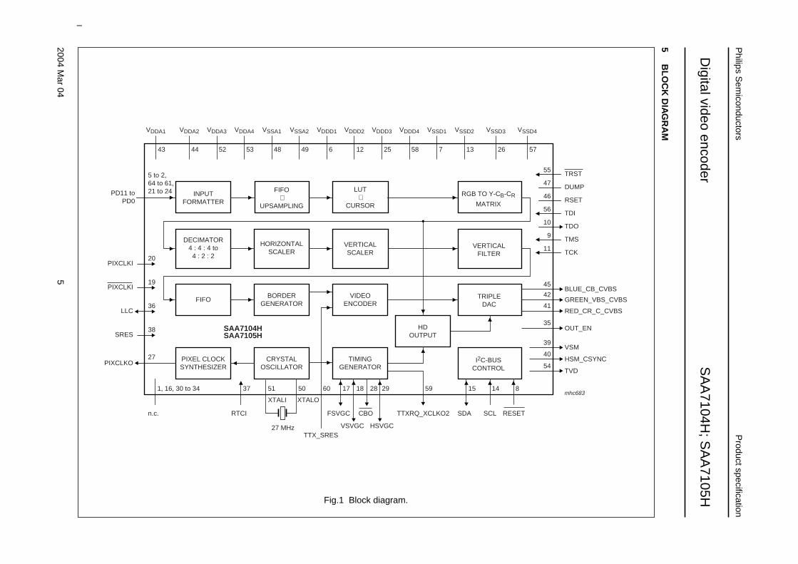
Fig.1 Block diagram.
Philips Semiconductors Product specification
Digital video encoder SAA7104H; SAA7105H
6 PINNING
SYMBOL PIN TYPE (1) DESCRIPTION
n.c. 1 − not connected
PD8 2 I see Tables 8 to 13 for pin assignment
PD9 3 I see Tables 8 to 13 for pin assignment
PD10 4 I see Tables 8 to 13 for pin assignment
PD11 5 I see Tables 8 to 13 for pin assignment
VDDD1 6 S digital supply voltage 1 for pins PD11 to PD0, PIXCLKI, PIXCLKI, PIXCLKO,FSVGC, VSVGC, HSVGC, CBO and TVD
VSSD1 7 S digital ground 1
RESET 8 I reset input; active LOW
TMS 9 I/pu test mode select input for Boundary Scan Test (BST); note 2
TDO 10 O test data output for BST; note 2
TCK 11 I/pu test clock input for BST; note 2
VDDD2 12 S digital supply voltage 2 (3.3 V for I/Os)
VSSD2 13 S digital ground 2
SCL 14 I I2C-bus serial clock input
SDA 15 I/O I2C-bus serial data input/output
n.c. 16 − not connected
FSVGC 17 I/O frame synchronization output to Video Graphics Controller (VGC)(optional input); note 3
VSVGC 18 I/O vertical synchronization output to VGC (optional input); note 3
PIXCLKI 19 I inverted pixel clock input
PIXCLKI 20 I pixel clock input (looped through)
PD3 21 I MSB − 4 with CB-Y-CR 4 : 2 : 2; see Tables 8 to 13 for pin assignment
PD2 22 I MSB − 5 with CB-Y-CR 4 : 2 : 2; see Tables 8 to 13 for pin assignment
PD1 23 I MSB − 6 with CB-Y-CR 4 : 2 : 2; see Tables 8 to 13 for pin assignment
PD0 24 I MSB − 7 with CB-Y-CR 4 : 2 : 2; see Tables 8 to 13 for pin assignment
VDDD3 25 S digital supply voltage 3 (3.3 V for core)
VSSD3 26 S digital ground 3
PIXCLKO 27 O pixel clock output to VGC
CBO 28 I/O composite blanking output to VGC; active LOW; note 3
HSVGC 29 I/O horizontal synchronization output to VGC (optional input); note 3
n.c. 30 − not connected
n.c. 31 − not connected
n.c. 32 − not connected
n.c. 33 − not connected
n.c. 34 − not connected
OUT_EN 35 I/pu if HIGH (default by pull-up): LLC, RTCI and SRES are outputs;if LOW: LLC, RTCI and SRES are inputs
LLC 36 I/O line-locked clock
RTCI 37 I/O real-time control input
2004 Mar 04 6
Philips Semiconductors Product specification
Digital video encoder SAA7104H; SAA7105H
Notes
1. Pin type: I = input, O = output, S = supply, pu = pull-up.
2. In accordance with the “IEEE1149.1” standard the pins TDI, TMS, TCK and TRST are input pins with an internalpull-up resistor and TDO is a 3-state output pin.
3. The pins FSVGC, VSVGC, CBO, HSVGC and TTXRQ_XCLKO2 are used for bootstrapping; see Section 7.1.
4. For board design without boundary scan implementation connect TRST to ground.
5. This pin provides easy initialization of the Boundary Scan Test (BST) circuit. TRST can be used to force the TestAccess Port (TAP) controller to the TEST_LOGIC_RESET state (normal operation) at once.
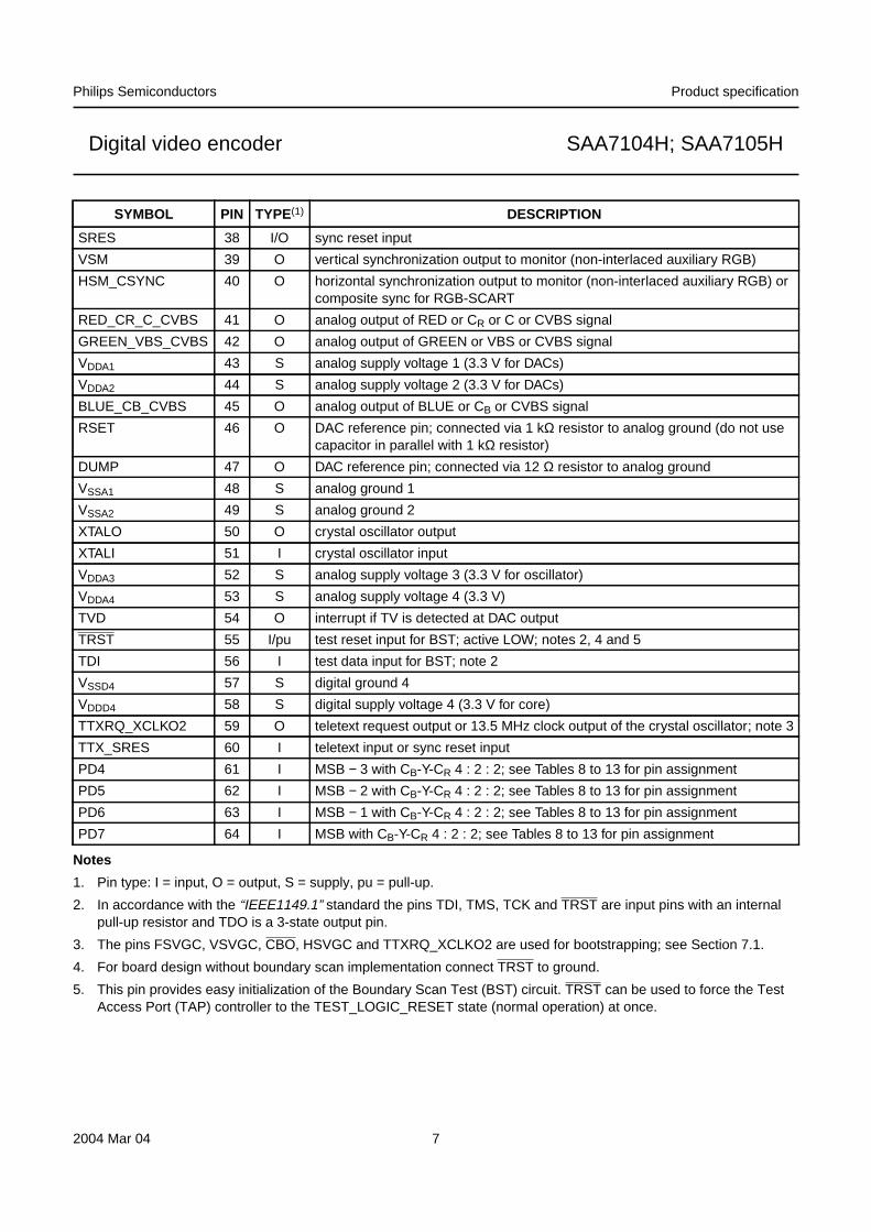
SRES 38 I/O sync reset input
VSM 39 O vertical synchronization output to monitor (non-interlaced auxiliary RGB)
HSM_CSYNC 40 O horizontal synchronization output to monitor (non-interlaced auxiliary RGB) orcomposite sync for RGB-SCART
RED_CR_C_CVBS 41 O analog output of RED or CR or C or CVBS signal
GREEN_VBS_CVBS 42 O analog output of GREEN or VBS or CVBS signal
VDDA1 43 S analog supply voltage 1 (3.3 V for DACs)
VDDA2 44 S analog supply voltage 2 (3.3 V for DACs)
BLUE_CB_CVBS 45 O analog output of BLUE or CB or CVBS signal
RSET 46 O DAC reference pin; connected via 1 kΩ resistor to analog ground (do not usecapacitor in parallel with 1 kΩ resistor)
DUMP 47 O DAC reference pin; connected via 12 Ω resistor to analog ground
VSSA1 48 S analog ground 1
VSSA2 49 S analog ground 2
XTALO 50 O crystal oscillator output
XTALI 51 I crystal oscillator input
VDDA3 52 S analog supply voltage 3 (3.3 V for oscillator)
VDDA4 53 S analog supply voltage 4 (3.3 V)
TVD 54 O interrupt if TV is detected at DAC output
TRST 55 I/pu test reset input for BST; active LOW; notes 2, 4 and 5
TDI 56 I test data input for BST; note 2
VSSD4 57 S digital ground 4
VDDD4 58 S digital supply voltage 4 (3.3 V for core)
TTXRQ_XCLKO2 59 O teletext request output or 13.5 MHz clock output of the crystal oscillator; note 3
TTX_SRES 60 I teletext input or sync reset input
PD4 61 I MSB − 3 with CB-Y-CR 4 : 2 : 2; see Tables 8 to 13 for pin assignment
PD5 62 I MSB − 2 with CB-Y-CR 4 : 2 : 2; see Tables 8 to 13 for pin assignment
PD6 63 I MSB − 1 with CB-Y-CR 4 : 2 : 2; see Tables 8 to 13 for pin assignment
PD7 64 I MSB with CB-Y-CR 4 : 2 : 2; see Tables 8 to 13 for pin assignment
SYMBOL PIN TYPE (1) DESCRIPTION
2004 Mar 04 7
Philips Semiconductors Product specification
Digital video encoder SAA7104H; SAA7105H
handbook, full pagewidth
n.c.
PD8
PD9
PD10
PD11
VDDD1
VSSD1
RESET
TMS
TDO
TCK
VDDD2
VSSD2
SCL
SDA
n.c.
VSSA1
DUMP
RSET
BLUE_CB_CVBS
VDDA2
VDDA1
GREEN_VBS_CVBS
RED_CR_C_CVBS
HSM_CSYNC
VSM
SRES
RTCI
LLC
OUT_EN
n.c.
n.c.
PD
7
PD
6
PD
5
PD
4
TT
X_S
RE
S
TT
XR
Q_X
CLK
O2
VD
DD
4
VS
SD
4
TD
I
TR
ST
TV
D
VD
DA
4
VD
DA
3
XT
ALI
XT
ALO
VS
SA
2
FS
VG
C
VS
VG
C
PIX
CLK
I
PIX
CLK
I
PD
3
PD
2
PD
1
PD
0
VD
DD
3
VS
SD
3
PIX
CLK
O
CB
O
HS
VG
C
n.c.
n.c.
n.c.
SAA7104HSAA7105H
MHC684
1
2
3
4
5
6
7
8
9
10
11
12
13
14
15
16
48
47
46
45
44
43
42
41
40
39
38
37
36
35
34
33
17 18 19 20 21 22 23 24 25 26 27 28 29 30 31 32
64 63 62 61 60 59 58 57 56 55 54 53 52 51 50 49
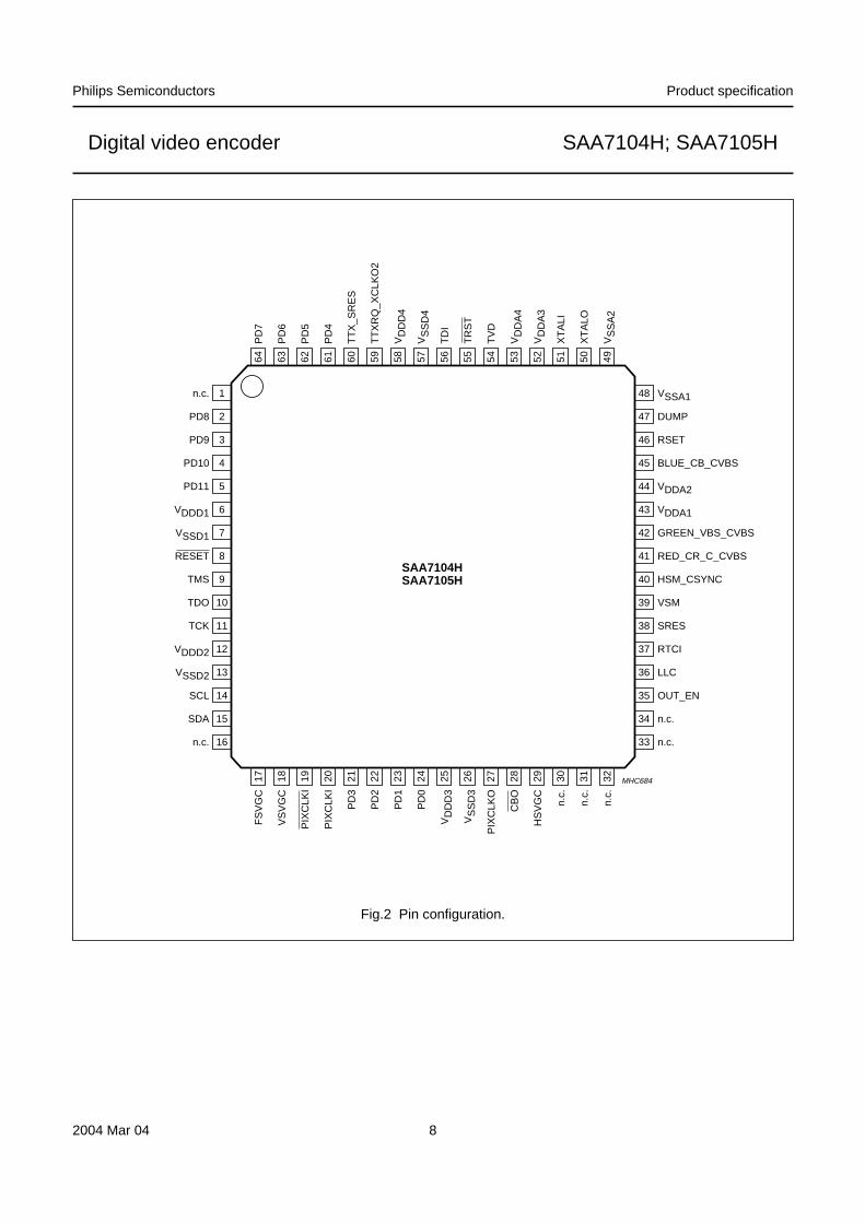
Fig.2 Pin configuration.
2004 Mar 04 8
Philips Semiconductors Product specification
Digital video encoder SAA7104H; SAA7105H
7 FUNCTIONAL DESCRIPTION
The digital video encoder encodes digital luminance andcolour difference signals (CB-Y-CR) or digital RGB signalsinto analog CVBS, S-video and, optionally, RGB orCR-Y-CB signals. NTSC M, PAL B/G and sub-standardsare supported.
The SAA7104H; SAA7105H can be directly connected toa PC video graphics controller with a maximum resolutionof 1280 × 1024 (progressive) or 1920 × 1080 (interlaced)at a 50 or 60 Hz frame rate. A programmable scaler scalesthe computer graphics picture so that it will fit into astandard TV screen with an adjustable underscan area.Non-interlaced-to-interlaced conversion is optimized withan adjustable anti-flicker filter for a flicker-free display at avery high sharpness.
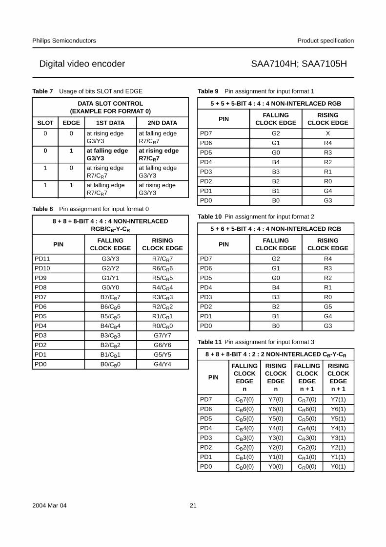
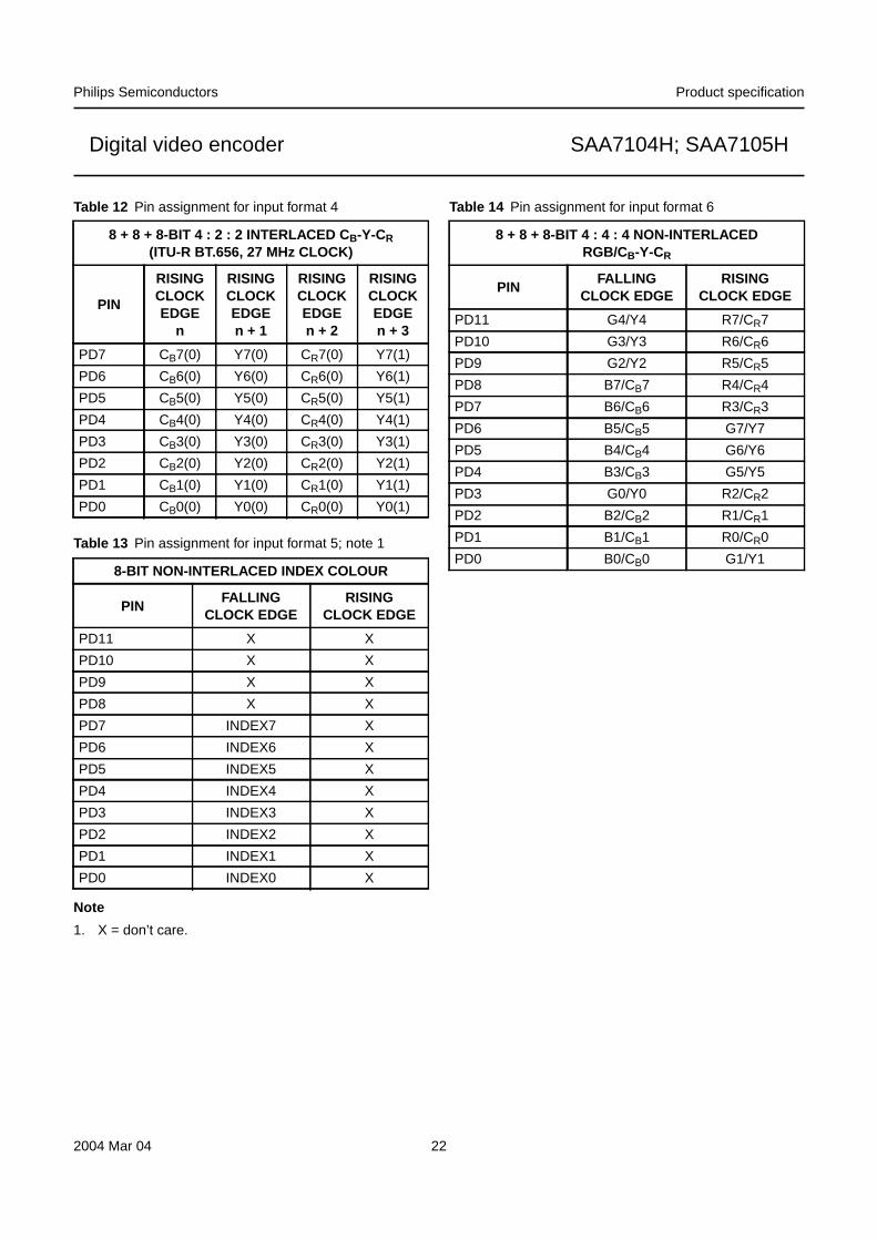
Besides the most common 16-bit 4 : 2 : 2 CB-Y-CR inputformat (using 8 pins with double edge clocking), otherCB-Y-CR and RGB formats are also supported; seeTables 8 to 13.
A complete 3 × 256 bytes Look-Up Table (LUT), which canbe used, for example, as a separate gamma corrector, islocated in the RGB domain; it can be loaded either throughthe video input port PD (Pixel Data) or via the I2C-bus.
The SAA7104H; SAA7105H supports a 32 × 32 × 2-bithardware cursor, the pattern of which can also be loadedthrough the video input port or via the I2C-bus.
It is also possible to encode interlaced 4 : 2 : 2 videosignals such as PC-DVD; for that the anti-flicker filter, andin most cases the scaler, will simply be bypassed.
Besides the applications for video output, the SAA7104H;SAA7105H can also be used for generating a kind ofauxiliary VGA output, when the RGB non-interlaced inputsignal is fed to the DACs. This may be of interest forexample, when the graphics controller provides a secondgraphics window at its video output port.
The basic encoder function consists of subcarriergeneration, colour modulation and insertion ofsynchronization signals at a crystal-stable clock rate of13.5 MHz (independent of the actual pixel clock used atthe input side), corresponding to an internal 4 : 2 : 2bandwidth in the luminance/colour difference domain.Luminance and chrominance signals are filtered inaccordance with the standard requirements of “RS-170-A”and “ITU-R BT.470-3”.
For ease of analog post filtering the signals are twiceoversampled to 27 MHz before digital-to-analogconversion.
The total filter transfer characteristics (scaler andanti-flicker filter are not taken into account) are illustratedin Figs 4 to 9. All three DACs are realized with full 10-bitresolution. The CR-Y-CB to RGB dematrix can bebypassed (optionally) in order to provide the upsampledCR-Y-CB input signals.
The 8-bit multiplexed CB-Y-CR formats are “ITU-R BT.656”(D1 format) compatible, but the SAV and EAV codes canbe decoded optionally, when the device is operated inslave mode. For assignment of the input data to the risingor falling clock edge see Tables 8 to 13.
In order to display interlaced RGB signals through aeuro-connector TV set, a separate digital composite syncsignal (pin HSM_CSYNC) can be generated; it can beadvanced up to 31 periods of the 27 MHz crystal clock inorder to be adapted to the RGB processing of a TV set.
The SAA7104H; SAA7105H synthesizes all necessaryinternal signals, colour subcarrier frequency andsynchronization signals from that clock.
It is also possible to connect a Philips digital video decoder(e.g. SAA7114H), using its line-locked clock forre-encoding. Information containing actual subcarrier,PAL-ID etc. is provided via pin RTCI which is connected topin RTCO of the decoder.
Wide screen signalling data can be loaded via the I2C-busand is inserted into line 23 for standards using a 50 Hzfield rate.
VPS data for program dependent automatic start and stopof such featured VCRs is loadable via the I2C-bus.
The IC also contains Closed Caption and extended dataservices encoding (line 21), and supports teletext insertionfor the appropriate bit stream format at a 27 MHz clock rate(see Fig.15). It is also possible to load data for the copygeneration management system into line 20 of every field(525/60 line counting).
A number of possibilities are provided for setting differentvideo parameters such as:
• Black and blanking level control
• Colour subcarrier frequency
• Variable burst amplitude etc.
2004 Mar 04 9
Philips Semiconductors Product specification
Digital video encoder SAA7104H; SAA7105H
7.1 Reset conditions
To activate the reset a pulse at least of 2 crystal clocksduration is required.
During reset (RESET = LOW) plus an extra 32 crystalclock periods, FSVGC, VSVGC, CBO, HSVGC andTTX_SRES are set to input mode and HSM_CSYNC andVSM are set to 3-state. A reset also forces the I2C-businterface to abort any running bus transfer and sets it intoreceive condition.
After reset, the state of the I/Os and other functions isdefined by the strapping pins until an I2C-bus accessredefines the corresponding registers; see Table 1.
Table 1 Strapping pins
7.2 Input formatter
The input formatter converts all accepted PD input dataformats, either RGB or Y-CB-CR, to a common internalRGB or Y-CB-CR data stream.
When double-edge clocking is used, the data is internallysplit into portions PPD1 and PPD2. The clock edgeassignment must be set according to the I2C-bus controlbits SLOT and EDGE for correct operation.
If Y-CB-CR is being applied as a 27 Mbyte/s data stream,the output of the input formatter can be used directly tofeed the video encoder block.
The horizontal upscaling is supported via the inputformatter. According to the programming of the pixel clockdividers (see Section 7.10), it will sample up the datastream to 1 ×, 2 × or 4 × the input data rate. An optionalinterpolation filter is available. The clock domain transitionis handled by a 4 entries wide FIFO which gets initializedevery field or explicitly at request. A bypass for the FIFO isavailable, especially for high input data rates.
7.3 RGB LUT
The three 256 byte RAMs of this block can be addressedby three 8-bit wide signals, thus it can be used to build anytransformation, e.g. a gamma correction for RGB signals.In the event that the indexed colour data is applied, theRAMs are addressed in parallel.
The LUTs can either be loaded by an I2C-bus write accessor can be part of the pixel data input through the PD port.In the latter case, 256 × 3 bytes for the R, G and B LUT areexpected at the beginning of the input video line, two linesbefore the line that has been defined as first active line,until the middle of the line immediately preceding the firstactive line. The first 3 bytes represent the first RGB LUTdata, and so on.
7.4 Cursor insertion
A 32 × 32 dots cursor can be overlaid as an option; the bitmap of the cursor can be uploaded by an I2C-bus writeaccess to specific registers or in the pixel data inputthrough the PD port. In the latter case, the 256 bytesdefining the cursor bit map (2 bits per pixel) are expectedimmediately following the last RGB LUT data in the linepreceding the first active line.
The cursor bit map is set up as follows: each pixeloccupies 2 bits. The meaning of these bits depends on theCMODE I2C-bus register as described in Table 4.Transparent means that the input pixels are passedthrough, the ‘cursor colours’ can be programmed inseparate registers.
The bit map is stored with 4 pixels per byte, aligned to theleast significant bit. So the first pixel is in bits 0 and 1, thenext pixel in bits 3 and 4 and so on. The first index is thecolumn, followed by the row; index 0,0 is the upper leftcorner.
PIN TIED PRESET
FSVGC LOW NTSC M encoding, PIXCLKfits to 640 × 480 graphicsinput
HIGH PAL B/G encoding, PIXCLKfits to 640 × 480 graphicsinput
VSVGC LOW 4 : 2 : 2 Y-CB-CR graphicsinput (format 0)
HIGH 4 : 4 : 4 RGB graphics input(format 3)
CBO LOW input demultiplex phase:LSB = LOW
HIGH input demultiplex phase:LSB = HIGH
HSVGC LOW input demultiplex phase:MSB = LOW
HIGH input demultiplex phase:MSB = HIGH
TTXRQ_XCLKO2 LOW slave (FSVGC, VSVGC andHSVGC are inputs, internalcolour bar is active)
HIGH master (FSVGC, VSVGCand HSVGC are outputs)
2004 Mar 04 10
Philips Semiconductors Product specification
Digital video encoder SAA7104H; SAA7105H
Table 2 Layout of a byte in the cursor bit map
For each direction, there are 2 registers controlling theposition of the cursor, one controls the position of the‘hot spot’, the other register controls the insertion position.The hot spot is the ‘tip’ of the pointer arrow. It can have anyposition in the bit map. The actual position registersdescribe the co-ordinates of the hot spot. Again 0,0 is theupper left corner. While it is not possible to move thehot spot beyond the left respectively upper screen borderthis is perfectly legal for the right respectively lower border.It should be noted that the cursor position is describedrelative to the input resolution.
Table 3 Cursor bit map
Table 4 Cursor modes
7.5 RGB Y-CB-CR matrix
RGB input signals to be encoded to PAL or NTSC areconverted to the Y-CB-CR colour space in this block. Thecolour difference signals are fed through low-pass filtersand formatted to a ITU-R BT.601 like 4 : 2 : 2 data streamfor further processing.
A gain adjust option corrects the level swing of thegraphics world (black-to-white as 0 to 255) to the requiredrange of 16 to 235.
The matrix and formatting blocks can be bypassed forY-CB-CR graphics input.
When the auxiliary VGA mode is selected, the output of thecursor insertion block is immediately directed to the tripleDAC.
7.6 Horizontal scaler
The high quality horizontal scaler operates on the 4 : 2 : 2data stream. Its control engines compensate the colourphase offset automatically.
The scaler starts processing after a programmablehorizontal offset and continues with a number of inputpixels. Each input pixel is a programmable fraction of thecurrent output pixel (XINC/4096). A special case isXINC = 0, this sets the scaling factor to 1.
If the SAA7104H; SAA7105H input data is in accordancewith “ITU-R BT.656”, the scaler enters another mode.In this event, XINC needs to be set to 2048 for a scalingfactor of 1. With higher values, upscaling will occur.
The phase resolution of the circuit is 12 bits, giving amaximum offset of 0.2 after 800 input pixels. Small FIFOsrearrange a 4 : 2 : 2 data stream at the scaler output.
D7 D6 D5 D4 D3 D2 D1 D0
pixel n + 3 pixel n + 2 pixel n + 1 pixel n
D1 D0 D1 D0 D1 D0 D1 D0
BYTE D7 D6 D5 D4 D3 D2 D1 D0
0 row 0column 3
row 0column 2
row 0column 1
row 0column 0
1 row 0column 7
row 0column 6
row 0column 5
row 0column 4
2 row 0column11
row 0column10
row 0column 9
row 0column 8
... ... ... ... ...
6 row 0column27
row 0column26
row 0column25
row 0column24
7 row 0column31
row 0column30
row 0column29
row 0column28
... ... ... ... ...
254 row 31column27
row 31column26
row 31column25
row 31column24
255 row 31column31
row 31column30
row 31column29
row 31column28
CURSORPATTERN
CURSOR MODE
CMODE = 0 CMODE = 1
00 second cursor colour second cursor colour
01 first cursor colour first cursor colour
10 transparent transparent
11 inverted input auxiliary cursorcolour
2004 Mar 04 11
Philips Semiconductors Product specification
Digital video encoder SAA7104H; SAA7105H
7.7 Vertical scaler and anti-flicker filter
The functions scaling, Anti-Flicker Filter (AFF) andre-interlacing are implemented in the vertical scaler.
Besides the entire input frame, it receives the first and lastlines of the border to allow anti-flicker filtering.
The circuit generates the interlaced output fields by scalingdown the input frames with different offsets for odd andeven fields. Increasing the YSKIP setting reduces theanti-flicker function. A YSKIP value of 4095 switches it off;see Table 85.
An additional, programmable vertical filter supports theanti-flicker function. This filter is not available at upscalingfactors of more than 2.
The programming is similar to the horizontal scaler. For there-interlacing, the resolutions of the offset registers are notsufficient, so the weighting factors for the first lines canalso be adjusted. YINC = 0 sets the scaling factor to 1;YIWGTO and YIWGTE must not be 0.
Due to the re-interlacing, the circuit can perform upscalingby a maximum factor of 2. The maximum factor dependson the setting of the anti-flicker function and can be derivedfrom the formulae given in Section 7.20.
An additional upscaling mode allows to increase theupscaling factor to maximum 4 as it is required for the oldVGA modes like 320 × 240.
7.8 FIFO
The FIFO acts as a buffer to translate from the PIXCLKclock domain to the XTAL clock domain. The write clock isPIXCLK and the read clock is XTAL. An underflow oroverflow condition can be detected via the I2C-bus readaccess.
In order to avoid underflows and overflows, it is essentialthat the frequency of the synthesized PIXCLK matches tothe input graphics resolution and the desired scalingfactor.
7.9 Border generator
When the graphics picture is to be displayed as interlacedPAL, NTSC, S-video or RGB on a TV screen, it is desiredin many cases not to lose picture information due to theinherent overscanning of a TV set. The desired amount ofunderscan area, which is achieved through appropriatescaling in the vertical and horizontal direction, can be filledin the border generator with an arbitrary true colour tint.
7.10 Oscillator and Discrete Time Oscillator (DTO)
The master clock generation is realized as a 27 MHzcrystal oscillator, which can operate with either afundamental wave crystal or a 3rd-harmonic crystal.
The crystal clock supplies the DTO of the pixel clocksynthesizer, the video encoder and the I2C-bus controlblock. It also usually supplies the triple DAC, with theexception of the auxiliary VGA or HDTV mode, where thetriple DAC is clocked by the pixel clock (PIXCLK).
The DTO can be programmed to synthesize all relevantpixel clock frequencies between circa 40 and 85 MHz.Two programmable dividers provide the actual clock to beused externally and internally. The dividers can beprogrammed to factors of 1, 2, 4 and 8. For the internalpixel clock, a divider ratio of 8 makes no sense and is thusforbidden.
The internal clock can be switched completely to the pixelclock input. In this event, the input FIFO is useless and willbe bypassed.
The entire pixel clock generation can be locked to thevertical frequency. Both pixel clock dividers getre-initialized every field. Optionally, the DTO can becleared with each V-sync. At proper programming, this willmake the pixel clock frequency a precise multiple of thevertical and horizontal frequencies. This is required forsome graphic controllers.
7.11 Low-pass Clock Generation Circuit (CGC)
This block reduces the phase jitter of the synthesized pixelclock. It works as a tracking filter for all relevantsynthesized pixel clock frequencies.
7.12 Encoder
7.12.1 VIDEO PATH
The encoder generates luminance and colour subcarrieroutput signals from the Y, CB and CR baseband signals,which are suitable for use as CVBS or separate Y and Csignals.
Input to the encoder, at 27 MHz clock (e.g. DVD), is eitheroriginated from computer graphics at pixel clock, fedthrough the FIFO and border generator, or a ITU-R BT.656style signal.
2004 Mar 04 12
Philips Semiconductors Product specification
Digital video encoder SAA7104H; SAA7105H
Luminance is modified in gain and in offset (the offset isprogrammable in a certain range to enable different blacklevel set-ups). A blanking level can be set after insertion ofa fixed synchronization pulse tip level, in accordance withstandard composite synchronization schemes. Othermanipulations used for the Macrovision anti-tapingprocess, such as additional insertion of AGC super-whitepulses (programmable in height), are supported by theSAA7104H only.
To enable easy analog post filtering, luminance isinterpolated from a 13.5 MHz data rate to a 27 MHz datarate, thereby providing luminance in a 10-bit resolution.The transfer characteristics of the luminance interpolationfilter are illustrated in Figs 6 and 7. Appropriate transientsat start/end of active video and for synchronization pulsesare ensured.
Chrominance is modified in gain (programmableseparately for CB and CR), and a standard dependentburst is inserted, before baseband colour signals areinterpolated from a 6.75 MHz data rate to a 27 MHz datarate. One of the interpolation stages can be bypassed,thus providing a higher colour bandwidth, which can beused for the Y and C output. The transfer characteristics ofthe chrominance interpolation filter are illustrated inFigs 4 and 5.
The amplitude (beginning and ending) of the insertedburst, is programmable in a certain range that is suitablefor standard signals and for special effects. After thesucceeding quadrature modulator, colour is provided onthe subcarrier in 10-bit resolution.
The numeric ratio between the Y and C outputs is inaccordance with the standards.
7.12.2 TELETEXT INSERTION AND ENCODING (NOT
SIMULTANEOUSLY WITH REAL-TIME CONTROL)
Pin TTX_SRES receives a WST or NABTS teletextbitstream sampled at the crystal clock. At each rising edgeof the output signal (TTXRQ) a single teletext bit has to beprovided after a programmable delay at input pinTTX_SRES.
Phase variant interpolation is achieved on this bitstream inthe internal teletext encoder, providing sufficient smallphase jitter on the output text lines.
TTXRQ_XCLKO2 provides a fully programmable requestsignal to the teletext source, indicating the insertion periodof bitstream at lines which can be selected independently
for both fields. The internal insertion window for text is setto 360 (PAL WST), 296 (NTSC WST) or 288 (NABTS)teletext bits including clock run-in bits. The protocol andtiming are illustrated in Fig.15.
Alternatively, this pin can be provided with a bufferedcrystal clock (XCLK) of 13.5 MHz.
7.12.3 VIDEO PROGRAMMING SYSTEM (VPS) ENCODING
Five bytes of VPS information can be loaded via theI2C-bus and will be encoded in the appropriate format intoline 16.
7.12.4 CLOSED CAPTION ENCODER
Using this circuit, data in accordance with the specificationof Closed Caption or extended data service, delivered bythe control interface, can be encoded (line 21). Twodedicated pairs of bytes (two bytes per field), each pairpreceded by run-in clocks and framing code, are possible.
The actual line number in which data is to be encoded, canbe modified in a certain range.
The data clock frequency is in accordance with thedefinition for NTSC M standard 32 times horizontal linefrequency.
Data LOW at the output of the DACs corresponds to 0 IRE,data HIGH at the output of the DACs corresponds toapproximately 50 IRE.
It is also possible to encode Closed Caption data for 50 Hzfield frequencies at 32 times the horizontal line frequency.
7.12.5 ANTI-TAPING (SAA7104H ONLY)
For more information contact your nearest PhilipsSemiconductors sales office.
7.13 RGB processor
This block contains a dematrix in order to produce RED,GREEN and BLUE signals to be fed to a SCART plug.
Before Y, CB and CR signals are de-matrixed, individualgain adjustment for Y and colour difference signals and2 times oversampling for luminance and 4 timesoversampling for colour difference signals is performed.The transfer curves of luminance and colour differencecomponents of RGB are illustrated in Figs 8 and 9.
2004 Mar 04 13
Philips Semiconductors Product specification
Digital video encoder SAA7104H; SAA7105H
7.14 Triple DAC
Both Y and C signals are converted from digital-to-analogin a 10-bit resolution at the output of the video encoder.Y and C signals are also combined into a 10-bit CVBSsignal.
The CVBS output signal occurs with the same processingdelay as the Y, C and optional RGB or CR-Y-CB outputs.Absolute amplitude at the input of the DAC for CVBS isreduced by 15⁄16 with respect to Y and C DACs to makemaximum use of the conversion ranges.
RED, GREEN and BLUE signals are also converted fromdigital-to-analog, each providing a 10-bit resolution.
The reference currents of all three DACs can be adjustedindividually in order to adapt for different output signals.In addition, all reference currents can be adjustedcommonly to compensate for small tolerances of theon-chip band gap reference voltage.
Alternatively, all currents can be switched off to reducepower dissipation.
All three outputs can be used to sense for an external load(usually 75 Ω) during a pre-defined output. A flag in theI2C-bus status byte reflects whether a load is applied ornot. In addition, an automatic sense mode can beactivated which indicates a 75 Ω load at any of the threeoutputs at the dedicated interrupt pin TVD.
If the SAA7104H; SAA7105H is required to drive a second(auxiliary) VGA monitor or an HDTV set, the DACs receivethe signal coming from the HD data path. In this event, theDACs are clocked at the incoming PIXCLKI instead of the27 MHz crystal clock used in the video encoder.
7.15 HD data path
This data path allows the SAA7104H; SAA7105H to beused with VGA or HDTV monitors. It receives its datadirectly from the cursor generator and supports RGB andY-PB-PR output formats (RGB not with Y-PB-PR inputformats). No scaling is done in this mode.
A gain adjustment either leads the full level swing to thedigital-to-analog converters or reduces the amplitude by afactor of 0.69. This enables sync pulses to be added to thesignal as it is required for display units expecting signalswith sync pulses, either regular or 3-level syncs.
7.16 Timing generator
The synchronization of the SAA7104H; SAA7105H is ableto operate in two modes; slave mode and master mode.
In slave mode, the circuit accepts sync pulses on thebidirectional FSVGC (frame sync), VSVGC (vertical sync)and HSVGC (horizontal sync) pins: the polarities of thesignals can be programmed. The frame sync signal is onlynecessary when the input signal is interlaced, in othercases it may be omitted. If the frame sync signal is present,it is possible to derive the vertical and the horizontal phasefrom it by setting the HFS and VFS bits. HSVGC andVSVGC are not necessary in this case, so it is possible toswitch the pins to output mode.
Alternatively, the device can be triggered by auxiliarycodes in a ITU-R BT.656 data stream via PD7 to PD0.
Only vertical frequencies of 50 and 60 Hz are allowed withthe SAA7104H; SAA7105H. In slave mode, it is notpossible to lock the encoders colour carrier to the linefrequency with the PHRES bits.
In the (more common) master mode, the time base of thecircuit is continuously free-running. The IC can output aframe sync at pin FSVGC, a vertical sync at pin VSVGC, ahorizontal sync at pin HSVGC and a composite blankingsignal at pin CBO. All of these signals are defined in thePIXCLK domain. The duration of HSVGC and VSVGC arefixed, they are 64 clocks for HSVGC and 1 line for VSVGC.The leading slopes are in phase and the polarities can beprogrammed.
The input line length can be programmed. The field lengthis always derived from the field length of the encoder andthe pixel clock frequency that is being used.
CBO acts as a data request signal. The circuit acceptsinput data at a programmable number of clocks after CBOgoes active. This signal is programmable and it is possibleto adjust the following (see Figs 13 and 14):
• The horizontal offset
• The length of the active part of the line
• The distance from active start to first expected data
• The vertical offset separately for odd and even fields
• The number of lines per input field.
In most cases, the vertical offsets for odd and even fieldsare equal. If they are not, then the even field will start later.The SAA7104H; SAA7105H will also request the first inputlines in the even field, the total number of requested lineswill increase by the difference of the offsets.
As stated above, the circuit can be programmed to acceptthe look-up and cursor data in the first 2 lines of each field.The timing generator provides normal data request pulsesfor these lines; the duration is the same as for regular lines.
2004 Mar 04 14
Philips Semiconductors Product specification
Digital video encoder SAA7104H; SAA7105H
The additional request pulses will be suppressed withLUTL set to logic 0; see Table 108. The other verticaltimings do not change in this case, so the first active linecan be number 2, counted from 0.
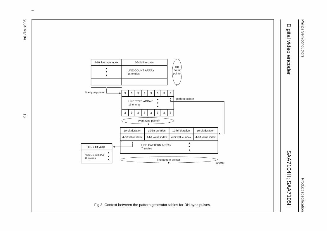
7.17 Pattern generator for HD sync pulses
The pattern generator provides appropriatesynchronization patterns for the video data path inauxiliary monitor or HDTV mode. It provides maximumflexibility in terms of raster generation for all interlaced andnon-interlaced computer graphics or ATSC formats. Thesync engine is capable of providing a combination ofevent-value pairs which can be used to insert certainvalues in the outgoing data stream at specified times.It can also be used to generate digital signals associatedwith time events. These can be used as digital horizontaland vertical synchronization signals on pins HSM_CSYNCand VSM.
The picture position is adjustable through theprogrammable relationship between the sync pulses andthe video contents.
The generation of embedded analog sync pulses is boundto a number of events which can be defined for a line.Several of these line timing definitions can exist in parallel.For the final sync raster composition a certain sequence oflines with different sync event properties has to be defined.The sequence specifies a series of line types and thenumber of occurrences of this specific line type. Once thesequence has been completed, it restarts from thebeginning. All pulse shapes are filtered internally in orderto avoid ringing after analog post filters.
The sequence of the generated pulse stream must fitprecisely to the incoming data stream in terms of the totalnumber of pixels per line and lines per frame.
The sync engines flexibility is achieved by using asequence of linked lists carrying the properties for the
image, the lines as well as fractions of lines. Figure 3illustrates the context between the various tables.
The first table serves as an array to hold the correctsequence of lines that compose the synchronizationraster; it can contain up to 16 entries. Each entry holds a4-bit index to the next table and a 10-bit counter valuewhich specifies how often this particular line is invoked.If the necessary line count for a particular line exceeds the10 bits, it has to use two table entries.
The 4-bit index in the line count array points to the line typearray. It holds up to 15 entries (index 0 is not used),index 1 points to the first entry, index 2 to the second entryof the line type array etc.
Each entry of the line type array can hold up to 8 indexpointers to another table. These indices point to portions ofa line pulse pattern: A line could be split up e.g. into a sync,a blank, and an active portion followed by another blankportion, occupying four entries in one table line.
Each index of this table points to a particular line of thenext table in the linked list. This table is called the linepattern array and each of the up to seven entries stores upto four pairs of a duration in pixel clock cycles and an indexto a value table. The table entries are used to defineportions of a line representing a certain value for a certainnumber of clock cycles.
The value specified in this table is actually another 3-bitindex into a value array which can hold up to eight 8-bitvalues. If bit 4 (MSB) of the index is logic 1, the value isinserted into the G or Y signal, only; if bit 4 = 0, theassociated value is inserted into all three signals.
Two additional bits of the entries in the value array (LSBsof the second byte) determine if the associated eventsappear as a digital pulse on the HSM_CSYNC and/or VSMoutputs.
2004 Mar 04 15
2004M
ar04
Philips S
emiconductors
Product specification
Digital video encoder
SA
A7104H
; SA
A7105H
This text is here in white to force landscape pages to be rotated correctly when browsing through the pdf in the Acrobat reader.This text is here in_white to force landscape pages to be rotated correctly when browsing through the pdf in the Acrobat reader.This text is here inThis text is here inwhite to force landscape pages to be rotated correctly when browsing through the pdf in the Acrobat reader. white to force landscape pages to be ...
HC573
16
handbook, full pagewidth
M
4-bit line type index
10-bit duration
4-bit value index
10-bit line count
LINE COUNT ARRAY16 entries
3 3 3 3 3 3 3 3
3 3 3 3 3 3 3 3
LINE TYPE ARRAY15 entries
VALUE ARRAY8 entries
LINE PATTERN ARRAY7 entries8 + 2-bit value
10-bit duration
4-bit value index
10-bit duration
4-bit value index
10-bit duration
4-bit value index
linecount
pointer
event type pointer
line pattern pointer
line type pointer
pattern pointer
Fig.3 Context between the pattern generator tables for DH sync pulses.
Philips Semiconductors Product specification
Digital video encoder SAA7104H; SAA7105H
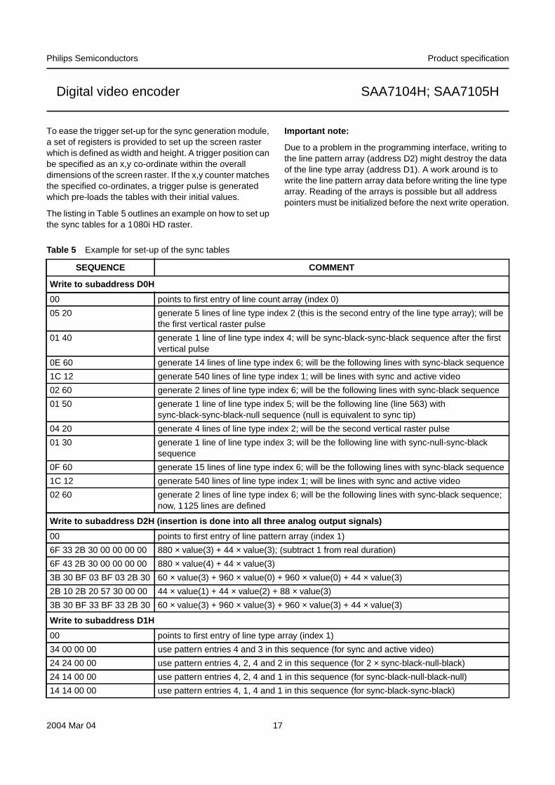
To ease the trigger set-up for the sync generation module,a set of registers is provided to set up the screen rasterwhich is defined as width and height. A trigger position canbe specified as an x,y co-ordinate within the overalldimensions of the screen raster. If the x,y counter matchesthe specified co-ordinates, a trigger pulse is generatedwhich pre-loads the tables with their initial values.
The listing in Table 5 outlines an example on how to set upthe sync tables for a 1080i HD raster.
Important note:
Due to a problem in the programming interface, writing tothe line pattern array (address D2) might destroy the dataof the line type array (address D1). A work around is towrite the line pattern array data before writing the line typearray. Reading of the arrays is possible but all addresspointers must be initialized before the next write operation.
Table 5 Example for set-up of the sync tables
SEQUENCE COMMENT
Write to subaddress D0H
00 points to first entry of line count array (index 0)
05 20 generate 5 lines of line type index 2 (this is the second entry of the line type array); will bethe first vertical raster pulse
01 40 generate 1 line of line type index 4; will be sync-black-sync-black sequence after the firstvertical pulse
0E 60 generate 14 lines of line type index 6; will be the following lines with sync-black sequence
1C 12 generate 540 lines of line type index 1; will be lines with sync and active video
02 60 generate 2 lines of line type index 6; will be the following lines with sync-black sequence
01 50 generate 1 line of line type index 5; will be the following line (line 563) withsync-black-sync-black-null sequence (null is equivalent to sync tip)
04 20 generate 4 lines of line type index 2; will be the second vertical raster pulse
01 30 generate 1 line of line type index 3; will be the following line with sync-null-sync-blacksequence
0F 60 generate 15 lines of line type index 6; will be the following lines with sync-black sequence
1C 12 generate 540 lines of line type index 1; will be lines with sync and active video
02 60 generate 2 lines of line type index 6; will be the following lines with sync-black sequence;now, 1125 lines are defined
Write to subaddress D2H (insertion is done into all three analog output signals)
00 points to first entry of line pattern array (index 1)
6F 33 2B 30 00 00 00 00 880 × value(3) + 44 × value(3); (subtract 1 from real duration)
6F 43 2B 30 00 00 00 00 880 × value(4) + 44 × value(3)
3B 30 BF 03 BF 03 2B 30 60 × value(3) + 960 × value(0) + 960 × value(0) + 44 × value(3)
2B 10 2B 20 57 30 00 00 44 × value(1) + 44 × value(2) + 88 × value(3)
3B 30 BF 33 BF 33 2B 30 60 × value(3) + 960 × value(3) + 960 × value(3) + 44 × value(3)
Write to subaddress D1H
00 points to first entry of line type array (index 1)
34 00 00 00 use pattern entries 4 and 3 in this sequence (for sync and active video)
24 24 00 00 use pattern entries 4, 2, 4 and 2 in this sequence (for 2 × sync-black-null-black)
24 14 00 00 use pattern entries 4, 2, 4 and 1 in this sequence (for sync-black-null-black-null)
14 14 00 00 use pattern entries 4, 1, 4 and 1 in this sequence (for sync-black-sync-black)
2004 Mar 04 17
Philips Semiconductors Product specification
Digital video encoder SAA7104H; SAA7105H
14 24 00 00 use pattern entries 4, 1, 4 and 2 in this sequence (for sync-black-sync-black-null)
54 00 00 00 use pattern entries 4 and 5 in this sequence (for sync-black)
Write to subaddress D3H (no signals are directed to pins HSM_CSYNC and VSM)
00 points to first entry of value array (index 0)
CC 00 black level, to be added during active video
80 00 sync level LOW (minimum output voltage)
0A 00 sync level HIGH (3-level sync)
CC 00 black level (needed elsewhere)
80 00 null (identical to sync level LOW)
Write to subaddress DCH
0B insertion is active, gain for signal is adapted accordingly
SEQUENCE COMMENT
7.18 I2C-bus interface
The I2C-bus interface is a standard slave transceiver,supporting 7-bit slave addresses and 400 kbits/sguaranteed transfer rate. It uses 8-bit subaddressing withan auto-increment function. All registers are write andread, except two read only status bytes.
The register bit map consists of an RGB Look-Up Table(LUT), a cursor bit map and control registers. The LUTcontains three banks of 256 bytes, where each RGB tripletis assigned to one address. Thus a write access needs theLUT address and three data bytes following subaddressFFH. For further write access auto-incrementing of theLUT address is performed. The cursor bit map access issimilar to the LUT access but contains only a single byteper address.
The I2C-bus slave address is defined as 88H.
7.19 Power-down modes
In order to reduce the power consumption, the SAA7104H;SAA7105H supports 2 power-down modes, accessible viathe I2C-bus. The analog power-down mode (DOWNA = 1)turns off the digital-to-analog converters and the pixelclock synthesizer. The digital power-down mode turns offall internal clocks and sets the digital outputs to LOWexcept the I2C-bus interface. The IC keeps itsprogramming and can still be accessed in this mode,however not all registers can be read or written to. Readingor writing to the look-up tables, the cursor and the HD syncgenerator require a valid pixel clock. The typical supplycurrent in full power-down is approximately 5 mA.
Because the analog power-down mode turns off the pixelclock synthesizer, there are limitations in someapplications. If there is no pixel clock, the IC is not able toset its outputs to LOW. So, in most cases, DOWNA andDOWND should be set to logic 1 simultaneously. If theEIDIV bit is logic 1, it should be set to logic 0 beforepower-down.
7.20 Programming the SAA7104H; SAA7105H
The SAA7104H; SAA7105H needs to provide acontinuous data stream at its analog outputs as well asreceive a continuous stream of data from its data source.Because there is no frame memory isolating the datastreams, restrictions apply to the input frame timings.
Input and output processing of the SAA7104H; SAA7105Hare only coupled through the vertical frequencies. Inmaster mode, the encoder provides a vertical sync and anodd/even pulse to the input processing. In slave mode, theencoder receives them.
The parameters of the input field are mainly given by thememory capacity of the SAA7104H; SAA7105H. The ruleis that the scaler and thus the input processing needs toprovide the video data in the same time frames as theencoder reads them. Therefore, the vertical active videotimes (and the vertical frequencies) need to be the same.
The second rule is that there has to be data in the bufferFIFO when the encoder enters the active video area.Therefore, the vertical offset in the input path needs to bea bit shorter than the offset of the encoder.
2004 Mar 04 18
Philips Semiconductors Product specification
Digital video encoder SAA7104H; SAA7105H
The following Sections give the set of equations requiredto program the IC for the most common application: A postprocessor in master mode with non-interlaced video inputdata.
Some variables are defined below:
• InPix: the number of active pixels per input line
• InPpl: the length of the entire input line in pixel clocks
• InLin: the number of active lines per input field/frame
• TPclk: the pixel clock period
• RiePclk: the ratio of internal to external pixel clock
• OutPix: the number of active pixels per output line
• OutLin: the number of active lines per output field
• TXclk: the encoder clock period (37.037 ns).
7.20.1 TV DISPLAY WINDOW
At 60 Hz, the first visible pixel has the index 256,710 pixels can be encoded; at 50 Hz, the index is 284,702 pixels can be visible.
The output lines should be centred on the screen. It shouldbe noted that the encoder has 2 clocks per pixel;see Table 58.
ADWHS = 256 + 710 − OutPix (60 Hz);ADWHS = 284 + 702 − OutPix (50 Hz);ADWHE = ADWHS + OutPix × 2 (all frequencies)
For vertical, the procedure is the same. At 60 Hz, the firstline with video information is number 19, 240 lines can beactive. For 50 Hz, the numbers are 23 and 287;see Table 64.
(60 Hz);
(50 Hz);
LAL = FAL + OutLin (all frequencies)
Most TV sets use overscan, and not all pixels respectivelylines are visible. There is no standard for the factor, it ishighly recommended to make the number of output pixelsand lines adjustable. A reasonable underscan factor is10%, giving approximately 640 output pixels per line.
7.20.2 INPUT FRAME AND PIXEL CLOCK
The total number of pixel clocks per line and the inputhorizontal offset need to be chosen next. The onlyconstraint is that the horizontal blanking has at least10 clock pulses.
The required pixel clock frequency can be determined inthe following way: Due to the limited internal FIFO size, theinput path has to provide all pixels in the same time frameas the encoders vertical active time. The scaler also has toprocess the first and last border lines for the anti-flickerfunction. Thus:
(60 Hz)
(50 Hz)
and for the pixel clock generator
(all frequencies);
see Tables 67, 69 and 70. The divider PCLE should be setaccording to Table 69. PCLI may be set to a lower or thesame value. Setting a lower value means that the internalpixel clock is higher and the data get sampled up. Thedifference may be 1 at 640 × 480 pixels resolution and 2 atresolutions with 320 pixels per line as a rule of thumb. Thisallows horizontal upscaling by a maximum factor of 2respectively 4 (this is the parameter RiePclk).
(all frequencies)
The equations ensure that the last line of the field has thefull number of clock cycles. Many graphic controllersrequire this. Note that the bit PCLSY needs to be set toensure that there is not even a fraction of a clock left at theend of the field.
7.20.3 HORIZONTAL SCALER
XOFS can be chosen arbitrarily, the condition being thatXOFS + XPIX ≤ HLEN is fulfilled. Values given by theVESA display timings are preferred.
HLEN = InPpl × RiePclk − 1
XINC needs to be rounded up, it needs to be set to 0 for ascaling factor of 1.
FAL 19 240 OutLin–2
---------------------------------+=
FAL 23 287 OutLin–2
---------------------------------+=
TPclk 262.5 1716× TXclk×
InPpl integerInLin 2+OutLin
---------------------- 262.5× ×
----------------------------------------------------------------------------------------=
TPclk 312.5 1728× TXclk×
InPpl integerInLin 2+OutLin
---------------------- 312.5× ×
----------------------------------------------------------------------------------------=
PCLTXclkTPclk--------------- 220 PCLE+×=
PCLI PCLE RiePclklog2log
----------------------------–=
XPIX InPix2
------------- RiePclk×=
XINC OutPixInPix
------------------4096
RiePclk--------------------×=
2004 Mar 04 19
Philips Semiconductors Product specification
Digital video encoder SAA7104H; SAA7105H
7.20.4 VERTICAL SCALER
The input vertical offset can be taken from the assumptionthat the scaler should just have finished writing the first linewhen the encoder starts reading it:
(60 Hz)
(50 Hz)
In most cases the vertical offsets will be the same for oddand even fields. The results should be rounded down.
YPIX = InLin
YSKIP defines the anti-flicker function. 0 means maximumflicker reduction but minimum vertical bandwidth, 4095gives no flicker reduction and maximum bandwidth. Notethat the maximum value for YINC is 4095. It might benecessary to reduce the value of YSKIP to fulfil thisrequirement.
When YINC = 0 it sets the scaler to scaling factor 1. Theinitial weighting factors must not be set to 0 in this case.YIWGTE may go negative. In this event, YINC should beadded and YOFSE incremented. This can be repeated asoften as necessary to make YIWGTE positive.
It should be noted that these equations assume that theinput is non-interlaced but the output is interlaced. If theinput is interlaced, the initial weighting factors need to beadapted to obtain the proper phase offsets in the outputframe.
If vertical upscaling beyond the upper capabilities isrequired, the parameter YUPSC may be set to logic 1. Thisextends the maximum vertical scaling factor by a factorof 2. Only the parameter YINC is affected, it needs to bedivided by two to get the same effect.
There are restrictions in this mode:
• The vertical filter YFILT is not available in this mode; thecircuit will ignore this value
• The horizontal blanking needs to be long enough totransfer an output line between 2 memory locations.This is 710 internal pixel clocks.
Or the upscaling factor needs to be limited to 1.5 and thehorizontal upscaling factor is also limited to less than∼1.5. In this case a normal blanking length is sufficient.
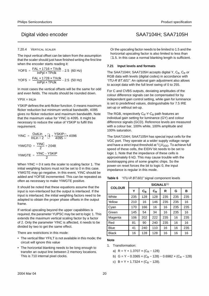
7.21 Input levels and formats
The SAA7104H; SAA7105H accepts digital Y, CB, CR orRGB data with levels (digital codes) in accordance with“ITU-R BT.601”. An optional gain adjustment also allowsto accept data with the full level swing of 0 to 255.
For C and CVBS outputs, deviating amplitudes of thecolour difference signals can be compensated for byindependent gain control setting, while gain for luminanceis set to predefined values, distinguishable for 7.5 IREset-up or without set-up.
The RGB, respectively CR-Y-CB path features anindividual gain setting for luminance (GY) and colourdifference signals (GCD). Reference levels are measuredwith a colour bar, 100% white, 100% amplitude and100% saturation.
The SAA7104H; SAA7105H has special input cells for theVGC port. They operate at a wider supply voltage rangeand have a strict input threshold at 1/2VDDD. To achieve fullspeed of these cells, the EIDIV bit needs to be set tologic 1. Note that the impedance of these cells isapproximately 6 kΩ. This may cause trouble with thebootstrapping pins of some graphic chips. So thepower-on reset forces the bit to logic 0, the inputimpedance is regular in this mode.
Table 6 “ITU-R BT.601” signal component levels
Note
1. Transformation:
a) R = Y + 1.3707 × (CR − 128)
b) G = Y − 0.3365 × (CB − 128) − 0.6982 × (CR − 128)
c) B = Y + 1.7324 × (CB − 128).
YOFS FAL 1716× TXclk×InPpl TPclk×---------------------------------------------------- 2.5–=
YOFS FAL 1728× TXclk×InPpl TPclk×---------------------------------------------------- 2.5–=
YINC OutLinInLin 2+---------------------- 1 YSKIP
4095-----------------+
× 4096×=
YIWGTO YINC2
-------------- 2048+=
YIWGTE YINC YSKIP–2
--------------------------------------=
COLOURSIGNALS (1)
Y CB CR R G B
White 235 128 128 235 235 235
Yellow 210 16 146 235 235 16
Cyan 170 166 16 16 235 235
Green 145 54 34 16 235 16
Magenta 106 202 222 235 16 235
Red 81 90 240 235 16 16
Blue 41 240 110 16 16 235
Black 16 128 128 16 16 16
2004 Mar 04 20
Philips Semiconductors Product specification
Digital video encoder SAA7104H; SAA7105H
Table 7 Usage of bits SLOT and EDGE
Table 8 Pin assignment for input format 0
Table 9 Pin assignment for input format 1
Table 10 Pin assignment for input format 2
Table 11 Pin assignment for input format 3
DATA SLOT CONTROL(EXAMPLE FOR FORMAT 0)
SLOT EDGE 1ST DATA 2ND DATA
0 0 at rising edgeG3/Y3
at falling edgeR7/CR7
0 1 at falling edgeG3/Y3
at rising edgeR7/CR7
1 0 at rising edgeR7/CR7
at falling edgeG3/Y3
1 1 at falling edgeR7/CR7
at rising edgeG3/Y3
8 + 8 + 8-BIT 4 : 4 : 4 NON-INTERLACEDRGB/CB-Y-CR
PINFALLING
CLOCK EDGERISING
CLOCK EDGE
PD11 G3/Y3 R7/CR7
PD10 G2/Y2 R6/CR6
PD9 G1/Y1 R5/CR5
PD8 G0/Y0 R4/CR4
PD7 B7/CB7 R3/CR3
PD6 B6/CB6 R2/CR2
PD5 B5/CB5 R1/CR1
PD4 B4/CB4 R0/CR0
PD3 B3/CB3 G7/Y7
PD2 B2/CB2 G6/Y6
PD1 B1/CB1 G5/Y5
PD0 B0/CB0 G4/Y4
5 + 5 + 5-BIT 4 : 4 : 4 NON-INTERLACED RGB
PINFALLING
CLOCK EDGERISING
CLOCK EDGE
PD7 G2 X
PD6 G1 R4
PD5 G0 R3
PD4 B4 R2
PD3 B3 R1
PD2 B2 R0
PD1 B1 G4
PD0 B0 G3
5 + 6 + 5-BIT 4 : 4 : 4 NON-INTERLACED RGB
PINFALLING
CLOCK EDGERISING
CLOCK EDGE
PD7 G2 R4
PD6 G1 R3
PD5 G0 R2
PD4 B4 R1
PD3 B3 R0
PD2 B2 G5
PD1 B1 G4
PD0 B0 G3
8 + 8 + 8-BIT 4 : 2 : 2 NON-INTERLACED CB-Y-CR
PIN
FALLINGCLOCKEDGE
n
RISINGCLOCKEDGE
n
FALLINGCLOCKEDGEn + 1
RISINGCLOCKEDGEn + 1
PD7 CB7(0) Y7(0) CR7(0) Y7(1)
PD6 CB6(0) Y6(0) CR6(0) Y6(1)
PD5 CB5(0) Y5(0) CR5(0) Y5(1)
PD4 CB4(0) Y4(0) CR4(0) Y4(1)
PD3 CB3(0) Y3(0) CR3(0) Y3(1)
PD2 CB2(0) Y2(0) CR2(0) Y2(1)
PD1 CB1(0) Y1(0) CR1(0) Y1(1)
PD0 CB0(0) Y0(0) CR0(0) Y0(1)
2004 Mar 04 21
Philips Semiconductors Product specification
Digital video encoder SAA7104H; SAA7105H
Table 12 Pin assignment for input format 4
Table 13 Pin assignment for input format 5; note 1
Note
1. X = don’t care.
Table 14 Pin assignment for input format 6
8 + 8 + 8-BIT 4 : 2 : 2 INTERLACED C B-Y-CR(ITU-R BT.656, 27 MHz CLOCK)
PIN
RISINGCLOCKEDGE
n
RISINGCLOCKEDGEn + 1
RISINGCLOCKEDGEn + 2
RISINGCLOCKEDGEn + 3
PD7 CB7(0) Y7(0) CR7(0) Y7(1)
PD6 CB6(0) Y6(0) CR6(0) Y6(1)
PD5 CB5(0) Y5(0) CR5(0) Y5(1)
PD4 CB4(0) Y4(0) CR4(0) Y4(1)
PD3 CB3(0) Y3(0) CR3(0) Y3(1)
PD2 CB2(0) Y2(0) CR2(0) Y2(1)
PD1 CB1(0) Y1(0) CR1(0) Y1(1)
PD0 CB0(0) Y0(0) CR0(0) Y0(1)
8-BIT NON-INTERLACED INDEX COLOUR
PINFALLING
CLOCK EDGERISING
CLOCK EDGE
PD11 X X
PD10 X X
PD9 X X
PD8 X X
PD7 INDEX7 X
PD6 INDEX6 X
PD5 INDEX5 X
PD4 INDEX4 X
PD3 INDEX3 X
PD2 INDEX2 X
PD1 INDEX1 X
PD0 INDEX0 X
8 + 8 + 8-BIT 4 : 4 : 4 NON-INTERLACEDRGB/CB-Y-CR
PINFALLING
CLOCK EDGERISING
CLOCK EDGE
PD11 G4/Y4 R7/CR7
PD10 G3/Y3 R6/CR6
PD9 G2/Y2 R5/CR5
PD8 B7/CB7 R4/CR4
PD7 B6/CB6 R3/CR3
PD6 B5/CB5 G7/Y7
PD5 B4/CB4 G6/Y6
PD4 B3/CB3 G5/Y5
PD3 G0/Y0 R2/CR2
PD2 B2/CB2 R1/CR1
PD1 B1/CB1 R0/CR0
PD0 B0/CB0 G1/Y1
2004 Mar 04 22
2004M
ar04
Philips S
emiconductors
Product specification
Digital video encoder
SA
A7104H
; SA
A7105H
This text is here in white to force landscape pages to be rotated correctly when browsing through the pdf in the Acrobat reader.This text is here in_white to force landscape pages to be rotated correctly when browsing through the pdf in the Acrobat reader.This text is here inThis text is here inwhite to force landscape pages to be rotated correctly when browsing through the pdf in the Acrobat reader. white to force landscape pages to be ...
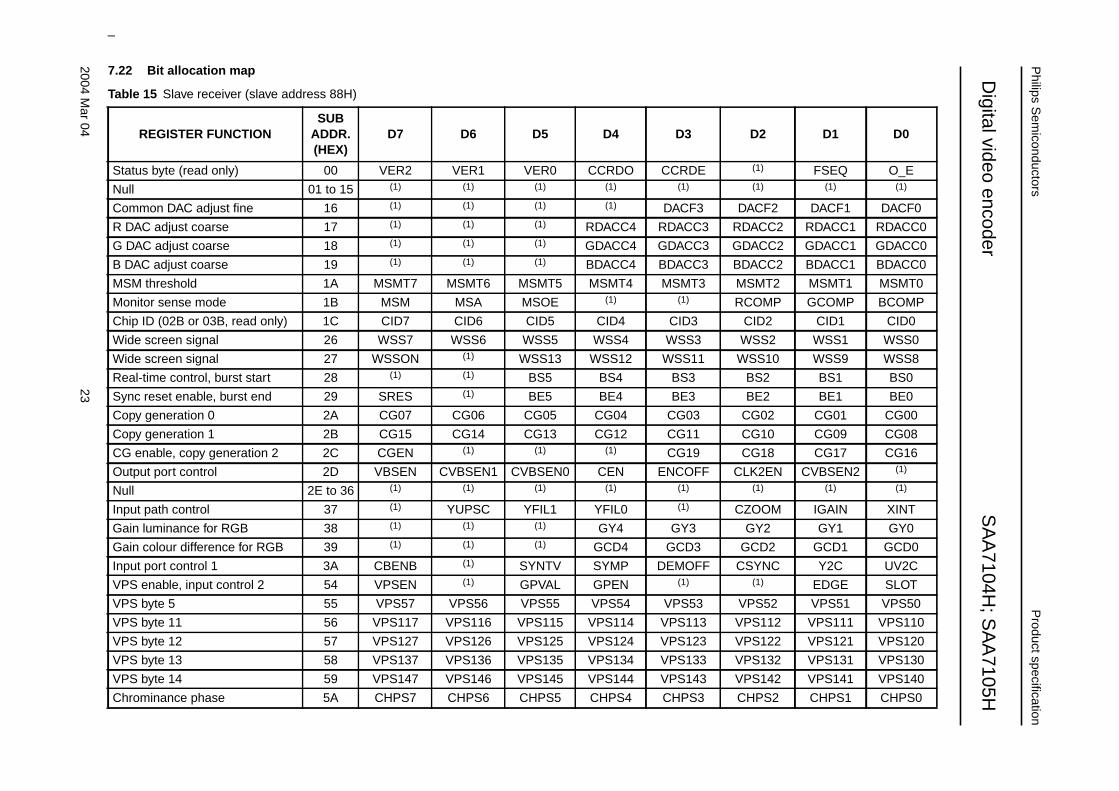
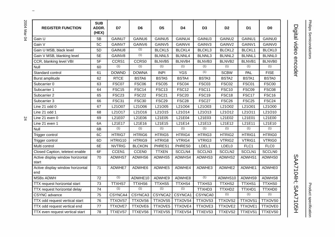
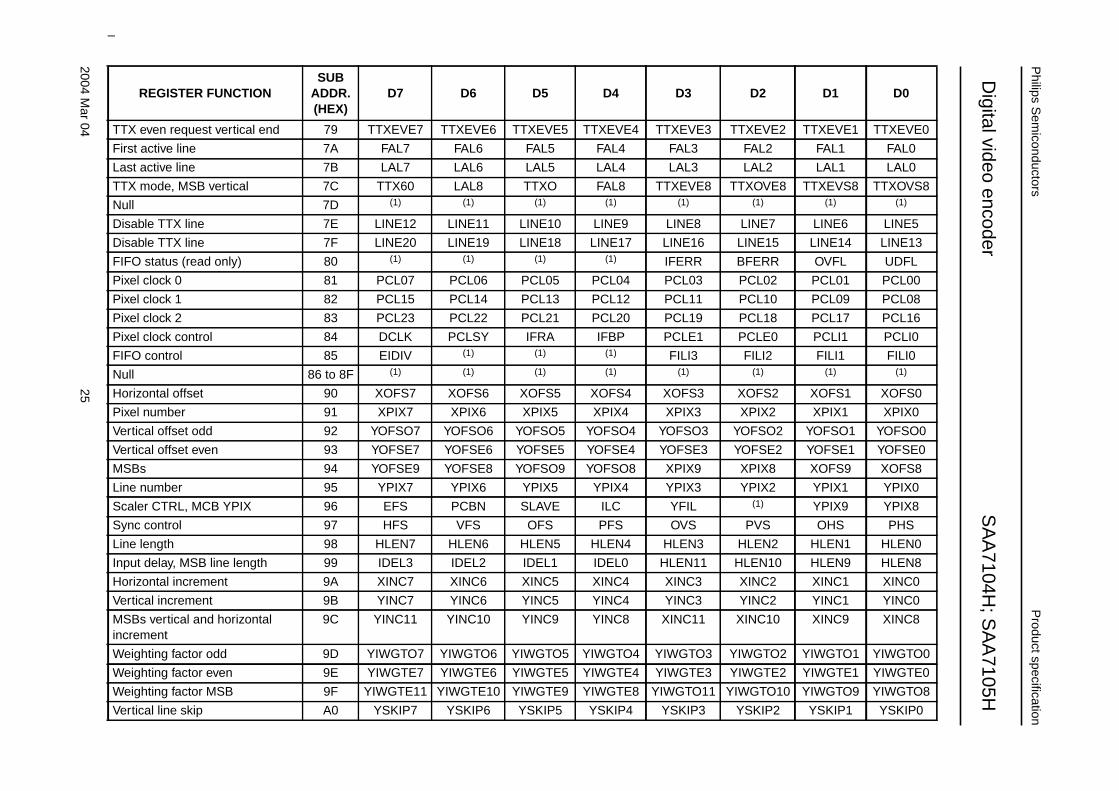
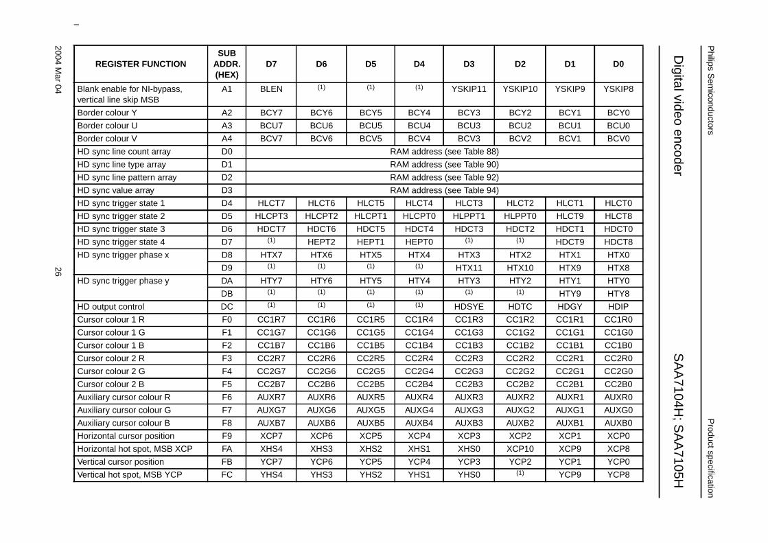
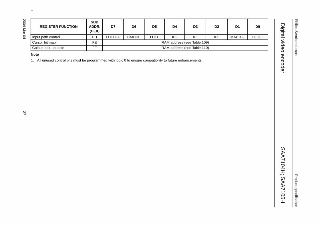
7.22 Bit allocation map
Table 15 Slave receiver (slave address 88H)
REGISTER FUNCTIONSUB
ADDR.(HEX)
D7 D6 D5 D4 D3 D2 D1 D0
(1) FSEQ O_E(1) (1) (1)
ACF2 DACF1 DACF0
DACC2 RDACC1 RDACC0
DACC2 GDACC1 GDACC0
DACC2 BDACC1 BDACC0
SMT2 MSMT1 MSMT0
COMP GCOMP BCOMP
CID2 CID1 CID0
WSS2 WSS1 WSS0
SS10 WSS9 WSS8
BS2 BS1 BS0
BE2 BE1 BE0
CG02 CG01 CG00
CG10 CG09 CG08
CG18 CG17 CG16
LK2EN CVBSEN2 (1)
(1) (1) (1)
ZOOM IGAIN XINT
GY2 GY1 GY0
GCD2 GCD1 GCD0
SYNC Y2C UV2C(1) EDGE SLOT
PS52 VPS51 VPS50
PS112 VPS111 VPS110
PS122 VPS121 VPS120
PS132 VPS131 VPS130
PS142 VPS141 VPS140
HPS2 CHPS1 CHPS0
23
Status byte (read only) 00 VER2 VER1 VER0 CCRDO CCRDE
Null 01 to 15 (1) (1) (1) (1) (1)
Common DAC adjust fine 16 (1) (1) (1) (1) DACF3 D
R DAC adjust coarse 17 (1) (1) (1) RDACC4 RDACC3 R
G DAC adjust coarse 18 (1) (1) (1) GDACC4 GDACC3 G
B DAC adjust coarse 19 (1) (1) (1) BDACC4 BDACC3 B
MSM threshold 1A MSMT7 MSMT6 MSMT5 MSMT4 MSMT3 M
Monitor sense mode 1B MSM MSA MSOE (1) (1) R
Chip ID (02B or 03B, read only) 1C CID7 CID6 CID5 CID4 CID3
Wide screen signal 26 WSS7 WSS6 WSS5 WSS4 WSS3
Wide screen signal 27 WSSON (1) WSS13 WSS12 WSS11 W
Real-time control, burst start 28 (1) (1) BS5 BS4 BS3
Sync reset enable, burst end 29 SRES (1) BE5 BE4 BE3
Copy generation 0 2A CG07 CG06 CG05 CG04 CG03
Copy generation 1 2B CG15 CG14 CG13 CG12 CG11
CG enable, copy generation 2 2C CGEN (1) (1) (1) CG19
Output port control 2D VBSEN CVBSEN1 CVBSEN0 CEN ENCOFF C
Null 2E to 36 (1) (1) (1) (1) (1)
Input path control 37 (1) YUPSC YFIL1 YFIL0 (1) C
Gain luminance for RGB 38 (1) (1) (1) GY4 GY3
Gain colour difference for RGB 39 (1) (1) (1) GCD4 GCD3
Input port control 1 3A CBENB (1) SYNTV SYMP DEMOFF C
VPS enable, input control 2 54 VPSEN (1) GPVAL GPEN (1)
VPS byte 5 55 VPS57 VPS56 VPS55 VPS54 VPS53 V
VPS byte 11 56 VPS117 VPS116 VPS115 VPS114 VPS113 V
VPS byte 12 57 VPS127 VPS126 VPS125 VPS124 VPS123 V
VPS byte 13 58 VPS137 VPS136 VPS135 VPS134 VPS133 V
VPS byte 14 59 VPS147 VPS146 VPS145 VPS144 VPS143 V
Chrominance phase 5A CHPS7 CHPS6 CHPS5 CHPS4 CHPS3 C
2004M
ar04
Philips S
emiconductors
Product specification
Digital video encoder
SA
A7104H
; SA
A7105H
This text is here in white to force landscape pages to be rotated correctly when browsing through the pdf in the Acrobat reader.This text is here in_white to force landscape pages to be rotated correctly when browsing through the pdf in the Acrobat reader.This text is here inThis text is here inwhite to force landscape pages to be rotated correctly when browsing through the pdf in the Acrobat reader. white to force landscape pages to be ...
Gain U 5B GAINU7 GAINU6 GAINU5 GAINU4 GAINU3 GAINU2 GAINU1 GAINU0
Gain V 5C GAINV7 GAINV6 GAINV5 GAINV4 GAINV3 GAINV2 GAINV1 GAINV0(1) LCKL2 BLCKL1 BLCKL0
LNNL2 BLNNL1 BLNNL0
LNVB2 BLNVB1 BLNVB0(1) (1) (1)
CBW PAL FISE
STA2 BSTA1 BSTA0
SC02 FSC01 FSC00
SC10 FSC09 FSC08
SC18 FSC17 FSC16
SC26 FSC25 FSC24
21O02 L21O01 L21O00
21O12 L21O11 L21O10
21E02 L21E01 L21E00
21E12 L21E11 L21E10(1) (1) (1)
TRIG2 HTRIG1 HTRIG0
TRIG2 VTRIG1 VTRIG0
DEL0 FLC1 FLC0
CCLN2 SCCLN1 SCCLN0
DWHS2 ADWHS1 ADWHS0
DWHE2 ADWHE1 ADWHE0
WHS10 ADWHS9 ADWHS8
TXHS2 TTXHS1 TTXHS0
TXHD2 TTXHD1 TTXHD0(1) (1) (1)
XOVS2 TTXOVS1 TTXOVS0
XOVE2 TTXOVE1 TTXOVE0
XEVS2 TTXEVS1 TTXEVS0
REGISTER FUNCTIONSUB
ADDR.(HEX)
D7 D6 D5 D4 D3 D2 D1 D0
24
Gain U MSB, black level 5D GAINU8 BLCKL5 BLCKL4 BLCKL3 B
Gain V MSB, blanking level 5E GAINV8 (1) BLNNL5 BLNNL4 BLNNL3 B
CCR, blanking level VBI 5F CCRS1 CCRS0 BLNVB5 BLNVB4 BLNVB3 B
Null 60 (1) (1) (1) (1) (1)
Standard control 61 DOWND DOWNA INPI YGS (1) S
Burst amplitude 62 RTCE BSTA6 BSTA5 BSTA4 BSTA3 B
Subcarrier 0 63 FSC07 FSC06 FSC05 FSC04 FSC03 F
Subcarrier 1 64 FSC15 FSC14 FSC13 FSC12 FSC11 F
Subcarrier 2 65 FSC23 FSC22 FSC21 FSC20 FSC19 F
Subcarrier 3 66 FSC31 FSC30 FSC29 FSC28 FSC27 F
Line 21 odd 0 67 L21O07 L21O06 L21O05 L21O04 L21O03 L
Line 21 odd 1 68 L21O17 L21O16 L21O15 L21O14 L21O13 L
Line 21 even 0 69 L21E07 L21E06 L21E05 L21E04 L21E03 L
Line 21 even 1 6A L21E17 L21E16 L21E15 L21E14 L21E13 L
Null 6B (1) (1) (1) (1) (1)
Trigger control 6C HTRIG7 HTRIG6 HTRIG5 HTRIG4 HTRIG3 H
Trigger control 6D HTRIG10 HTRIG9 HTRIG8 VTRIG4 VTRIG3 V
Multi control 6E NVTRIG BLCKON PHRES1 PHRES0 LDEL1 L
Closed Caption, teletext enable 6F CCEN1 CCEN0 TTXEN SCCLN4 SCCLN3 S
Active display window horizontalstart
70 ADWHS7 ADWHS6 ADWHS5 ADWHS4 ADWHS3 A
Active display window horizontalend
71 ADWHE7 ADWHE6 ADWHE5 ADWHE4 ADWHE3 A
MSBs ADWH 72 (1) ADWHE10 ADWHE9 ADWHE8 (1) AD
TTX request horizontal start 73 TTXHS7 TTXHS6 TTXHS5 TTXHS4 TTXHS3 T
TTX request horizontal delay 74 (1) (1) (1) (1) TTXHD3 T
CSYNC advance 75 CSYNCA4 CSYNCA3 CSYNCA2 CSYNCA1 CSYNCA0
TTX odd request vertical start 76 TTXOVS7 TTXOVS6 TTXOVS5 TTXOVS4 TTXOVS3 TT
TTX odd request vertical end 77 TTXOVE7 TTXOVE6 TTXOVE5 TTXOVE4 TTXOVE3 TT
TTX even request vertical start 78 TTXEVS7 TTXEVS6 TTXEVS5 TTXEVS4 TTXEVS3 TT
2004M
ar04
Philips S
emiconductors
Product specification
Digital video encoder
SA
A7104H
; SA
A7105H
This text is here in white to force landscape pages to be rotated correctly when browsing through the pdf in the Acrobat reader.This text is here in_white to force landscape pages to be rotated correctly when browsing through the pdf in the Acrobat reader.This text is here inThis text is here inwhite to force landscape pages to be rotated correctly when browsing through the pdf in the Acrobat reader. white to force landscape pages to be ...
TTX even request vertical end 79 TTXEVE7 TTXEVE6 TTXEVE5 TTXEVE4 TTXEVE3 TTXEVE2 TTXEVE1 TTXEVE0
First active line 7A FAL7 FAL6 FAL5 FAL4 FAL3 FAL2 FAL1 FAL0
LAL2 LAL1 LAL0
XOVE8 TTXEVS8 TTXOVS8(1) (1) (1)
LINE7 LINE6 LINE5
INE15 LINE14 LINE13
FERR OVFL UDFL
CL02 PCL01 PCL00
CL10 PCL09 PCL08
CL18 PCL17 PCL16
CLE0 PCLI1 PCLI0
FILI2 FILI1 FILI0(1) (1) (1)
OFS2 XOFS1 XOFS0
XPIX2 XPIX1 XPIX0
OFSO2 YOFSO1 YOFSO0
OFSE2 YOFSE1 YOFSE0
XPIX8 XOFS9 XOFS8
YPIX2 YPIX1 YPIX0(1) YPIX9 YPIX8
PVS OHS PHS
LEN2 HLEN1 HLEN0
LEN10 HLEN9 HLEN8
XINC2 XINC1 XINC0
YINC2 YINC1 YINC0
INC10 XINC9 XINC8
WGTO2 YIWGTO1 YIWGTO0
WGTE2 YIWGTE1 YIWGTE0
GTO10 YIWGTO9 YIWGTO8
SKIP2 YSKIP1 YSKIP0
REGISTER FUNCTIONSUB
ADDR.(HEX)
D7 D6 D5 D4 D3 D2 D1 D0
25
Last active line 7B LAL7 LAL6 LAL5 LAL4 LAL3
TTX mode, MSB vertical 7C TTX60 LAL8 TTXO FAL8 TTXEVE8 TT
Null 7D (1) (1) (1) (1) (1)
Disable TTX line 7E LINE12 LINE11 LINE10 LINE9 LINE8
Disable TTX line 7F LINE20 LINE19 LINE18 LINE17 LINE16 L
FIFO status (read only) 80 (1) (1) (1) (1) IFERR B
Pixel clock 0 81 PCL07 PCL06 PCL05 PCL04 PCL03 P
Pixel clock 1 82 PCL15 PCL14 PCL13 PCL12 PCL11 P
Pixel clock 2 83 PCL23 PCL22 PCL21 PCL20 PCL19 P
Pixel clock control 84 DCLK PCLSY IFRA IFBP PCLE1 P
FIFO control 85 EIDIV (1) (1) (1) FILI3
Null 86 to 8F (1) (1) (1) (1) (1)
Horizontal offset 90 XOFS7 XOFS6 XOFS5 XOFS4 XOFS3 X
Pixel number 91 XPIX7 XPIX6 XPIX5 XPIX4 XPIX3
Vertical offset odd 92 YOFSO7 YOFSO6 YOFSO5 YOFSO4 YOFSO3 Y
Vertical offset even 93 YOFSE7 YOFSE6 YOFSE5 YOFSE4 YOFSE3 Y
MSBs 94 YOFSE9 YOFSE8 YOFSO9 YOFSO8 XPIX9
Line number 95 YPIX7 YPIX6 YPIX5 YPIX4 YPIX3
Scaler CTRL, MCB YPIX 96 EFS PCBN SLAVE ILC YFIL
Sync control 97 HFS VFS OFS PFS OVS
Line length 98 HLEN7 HLEN6 HLEN5 HLEN4 HLEN3 H
Input delay, MSB line length 99 IDEL3 IDEL2 IDEL1 IDEL0 HLEN11 H
Horizontal increment 9A XINC7 XINC6 XINC5 XINC4 XINC3
Vertical increment 9B YINC7 YINC6 YINC5 YINC4 YINC3
MSBs vertical and horizontalincrement
9C YINC11 YINC10 YINC9 YINC8 XINC11 X
Weighting factor odd 9D YIWGTO7 YIWGTO6 YIWGTO5 YIWGTO4 YIWGTO3 YI
Weighting factor even 9E YIWGTE7 YIWGTE6 YIWGTE5 YIWGTE4 YIWGTE3 YI
Weighting factor MSB 9F YIWGTE11 YIWGTE10 YIWGTE9 YIWGTE8 YIWGTO11 YIW
Vertical line skip A0 YSKIP7 YSKIP6 YSKIP5 YSKIP4 YSKIP3 Y
2004M
ar04
Philips S
emiconductors
Product specification
Digital video encoder
SA
A7104H
; SA
A7105H
This text is here in white to force landscape pages to be rotated correctly when browsing through the pdf in the Acrobat reader.This text is here in_white to force landscape pages to be rotated correctly when browsing through the pdf in the Acrobat reader.This text is here inThis text is here inwhite to force landscape pages to be rotated correctly when browsing through the pdf in the Acrobat reader. white to force landscape pages to be ...
Blank enable for NI-bypass,vertical line skip MSB
A1 BLEN (1) (1) (1) YSKIP11 YSKIP10 YSKIP9 YSKIP8
Border colour Y A2 BCY7 BCY6 BCY5 BCY4 BCY3 BCY2 BCY1 BCY0
BCU2 BCU1 BCU0
BCV2 BCV1 BCV0
LCT2 HLCT1 HLCT0
LPPT0 HLCT9 HLCT8
DCT2 HDCT1 HDCT0(1) HDCT9 HDCT8
HTX2 HTX1 HTX0
TX10 HTX9 HTX8
HTY2 HTY1 HTY0(1) HTY9 HTY8
HDTC HDGY HDIP
C1R2 CC1R1 CC1R0
C1G2 CC1G1 CC1G0
C1B2 CC1B1 CC1B0
C2R2 CC2R1 CC2R0
C2G2 CC2G1 CC2G0
C2B2 CC2B1 CC2B0
UXR2 AUXR1 AUXR0
UXG2 AUXG1 AUXG0
UXB2 AUXB1 AUXB0
XCP2 XCP1 XCP0
CP10 XCP9 XCP8
YCP2 YCP1 YCP0(1) YCP9 YCP8
REGISTER FUNCTIONSUB
ADDR.(HEX)
D7 D6 D5 D4 D3 D2 D1 D0
26
Border colour U A3 BCU7 BCU6 BCU5 BCU4 BCU3
Border colour V A4 BCV7 BCV6 BCV5 BCV4 BCV3
HD sync line count array D0 RAM address (see Table 88)
HD sync line type array D1 RAM address (see Table 90)
HD sync line pattern array D2 RAM address (see Table 92)
HD sync value array D3 RAM address (see Table 94)
HD sync trigger state 1 D4 HLCT7 HLCT6 HLCT5 HLCT4 HLCT3 H
HD sync trigger state 2 D5 HLCPT3 HLCPT2 HLCPT1 HLCPT0 HLPPT1 H
HD sync trigger state 3 D6 HDCT7 HDCT6 HDCT5 HDCT4 HDCT3 H
HD sync trigger state 4 D7 (1) HEPT2 HEPT1 HEPT0 (1)
HD sync trigger phase x D8 HTX7 HTX6 HTX5 HTX4 HTX3
D9 (1) (1) (1) (1) HTX11 H
HD sync trigger phase y DA HTY7 HTY6 HTY5 HTY4 HTY3
DB (1) (1) (1) (1) (1)
HD output control DC (1) (1) (1) (1) HDSYE
Cursor colour 1 R F0 CC1R7 CC1R6 CC1R5 CC1R4 CC1R3 C
Cursor colour 1 G F1 CC1G7 CC1G6 CC1G5 CC1G4 CC1G3 C
Cursor colour 1 B F2 CC1B7 CC1B6 CC1B5 CC1B4 CC1B3 C
Cursor colour 2 R F3 CC2R7 CC2R6 CC2R5 CC2R4 CC2R3 C
Cursor colour 2 G F4 CC2G7 CC2G6 CC2G5 CC2G4 CC2G3 C
Cursor colour 2 B F5 CC2B7 CC2B6 CC2B5 CC2B4 CC2B3 C
Auxiliary cursor colour R F6 AUXR7 AUXR6 AUXR5 AUXR4 AUXR3 A
Auxiliary cursor colour G F7 AUXG7 AUXG6 AUXG5 AUXG4 AUXG3 A
Auxiliary cursor colour B F8 AUXB7 AUXB6 AUXB5 AUXB4 AUXB3 A
Horizontal cursor position F9 XCP7 XCP6 XCP5 XCP4 XCP3
Horizontal hot spot, MSB XCP FA XHS4 XHS3 XHS2 XHS1 XHS0 X
Vertical cursor position FB YCP7 YCP6 YCP5 YCP4 YCP3
Vertical hot spot, MSB YCP FC YHS4 YHS3 YHS2 YHS1 YHS0
2004M
ar04
Philips S
emiconductors
Product specification
Digital video encoder
SA
A7104H
; SA
A7105H
This text is here in white to force landscape pages to be rotated correctly when browsing through the pdf in the Acrobat reader.This text is here in_white to force landscape pages to be rotated correctly when browsing through the pdf in the Acrobat reader.This text is here inThis text is here inwhite to force landscape pages to be rotated correctly when browsing through the pdf in the Acrobat reader. white to force landscape pages to be ...
Input path control FD LUTOFF CMODE LUTL IF2 IF1 IF0 MATOFF DFOFF
Cursor bit map FE RAM address (see Table 109)
REGISTER FUNCTIONSUB
ADDR.(HEX)
D7 D6 D5 D4 D3 D2 D1 D0
27
Note
1. All unused control bits must be programmed with logic 0 to ensure compatibility to future enhancements.
Colour look-up table FF RAM address (see Table 110)
Philips Semiconductors Product specification
Digital video encoder SAA7104H; SAA7105H
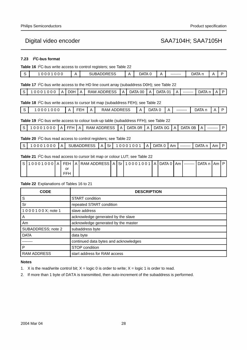
7.23 I2C-bus format
Table 16 I2C-bus write access to control registers; see Table 22
Table 17 I2C-bus write access to the HD line count array (subaddress D0H); see Table 22
Table 18 I2C-bus write access to cursor bit map (subaddress FEH); see Table 22
Table 19 I2C-bus write access to colour look-up table (subaddress FFH); see Table 22
Table 20 I2C-bus read access to control registers; see Table 22
Table 21 I2C-bus read access to cursor bit map or colour LUT; see Table 22
Table 22 Explanations of Tables 16 to 21
Notes
1. X is the read/write control bit; X = logic 0 is order to write; X = logic 1 is order to read.
2. If more than 1 byte of DATA is transmitted, then auto-increment of the subaddress is performed.
S 1 0 0 0 1 0 0 0 A SUBADDRESS A DATA 0 A -------- DATA n A P
S 1 0 0 0 1 0 0 0 A D0H A RAM ADDRESS A DATA 00 A DATA 01 A -------- DATA n A P
S 1 0 0 0 1 0 0 0 A FEH A RAM ADDRESS A DATA 0 A -------- DATA n A P
S 1 0 0 0 1 0 0 0 A FFH A RAM ADDRESS A DATA 0R A DATA 0G A DATA 0B A -------- P
S 1 0 0 0 1 0 0 0 A SUBADDRESS A Sr 1 0 0 0 1 0 0 1 A DATA 0 Am -------- DATA n Am P
S 1 0 0 0 1 0 0 0 A FEHor
FFH
A RAM ADDRESS A Sr 1 0 0 0 1 0 0 1 A DATA 0 Am -------- DATA n Am P
CODE DESCRIPTION
S START condition
Sr repeated START condition
1 0 0 0 1 0 0 X; note 1 slave address
A acknowledge generated by the slave
Am acknowledge generated by the master
SUBADDRESS; note 2 subaddress byte
DATA data byte
-------- continued data bytes and acknowledges
P STOP condition
RAM ADDRESS start address for RAM access
2004 Mar 04 28
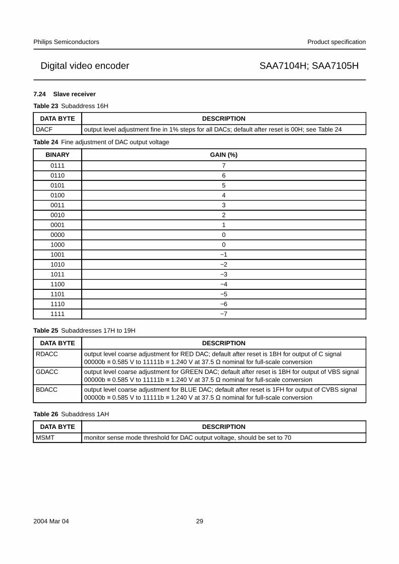
Philips Semiconductors Product specification
Digital video encoder SAA7104H; SAA7105H
7.24 Slave receiver
Table 23 Subaddress 16H
Table 24 Fine adjustment of DAC output voltage
Table 25 Subaddresses 17H to 19H
Table 26 Subaddress 1AH
DATA BYTE DESCRIPTION
DACF output level adjustment fine in 1% steps for all DACs; default after reset is 00H; see Table 24
BINARY GAIN (%)
0111 7
0110 6
0101 5
0100 4
0011 3
0010 2
0001 1
0000 0
1000 0
1001 −1
1010 −2
1011 −3
1100 −4
1101 −5
1110 −6
1111 −7
DATA BYTE DESCRIPTION
RDACC output level coarse adjustment for RED DAC; default after reset is 1BH for output of C signal00000b ≡ 0.585 V to 11111b ≡ 1.240 V at 37.5 Ω nominal for full-scale conversion
GDACC output level coarse adjustment for GREEN DAC; default after reset is 1BH for output of VBS signal00000b ≡ 0.585 V to 11111b ≡ 1.240 V at 37.5 Ω nominal for full-scale conversion
BDACC output level coarse adjustment for BLUE DAC; default after reset is 1FH for output of CVBS signal00000b ≡ 0.585 V to 11111b ≡ 1.240 V at 37.5 Ω nominal for full-scale conversion
DATA BYTE DESCRIPTION
MSMT monitor sense mode threshold for DAC output voltage, should be set to 70
2004 Mar 04 29
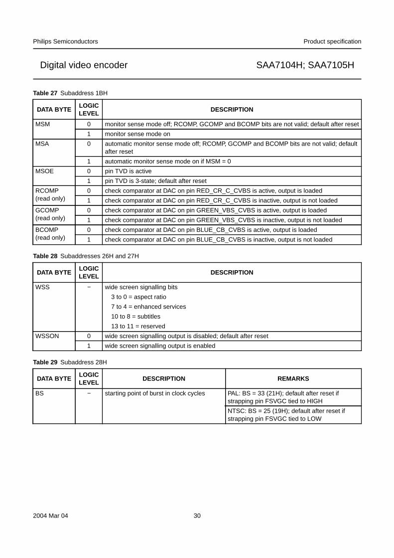
Philips Semiconductors Product specification
Digital video encoder SAA7104H; SAA7105H
Table 27 Subaddress 1BH
Table 28 Subaddresses 26H and 27H
Table 29 Subaddress 28H
DATA BYTELOGICLEVEL
DESCRIPTION
MSM 0 monitor sense mode off; RCOMP, GCOMP and BCOMP bits are not valid; default after reset
1 monitor sense mode on
MSA 0 automatic monitor sense mode off; RCOMP, GCOMP and BCOMP bits are not valid; defaultafter reset
1 automatic monitor sense mode on if MSM = 0
MSOE 0 pin TVD is active
1 pin TVD is 3-state; default after reset
RCOMP(read only)
0 check comparator at DAC on pin RED_CR_C_CVBS is active, output is loaded
1 check comparator at DAC on pin RED_CR_C_CVBS is inactive, output is not loaded
GCOMP(read only)
0 check comparator at DAC on pin GREEN_VBS_CVBS is active, output is loaded
1 check comparator at DAC on pin GREEN_VBS_CVBS is inactive, output is not loaded
BCOMP(read only)
0 check comparator at DAC on pin BLUE_CB_CVBS is active, output is loaded
1 check comparator at DAC on pin BLUE_CB_CVBS is inactive, output is not loaded
DATA BYTELOGICLEVEL
DESCRIPTION
WSS − wide screen signalling bits
3 to 0 = aspect ratio
7 to 4 = enhanced services
10 to 8 = subtitles
13 to 11 = reserved
WSSON 0 wide screen signalling output is disabled; default after reset
1 wide screen signalling output is enabled
DATA BYTELOGICLEVEL
DESCRIPTION REMARKS
BS − starting point of burst in clock cycles PAL: BS = 33 (21H); default after reset ifstrapping pin FSVGC tied to HIGH
NTSC: BS = 25 (19H); default after reset ifstrapping pin FSVGC tied to LOW
2004 Mar 04 30
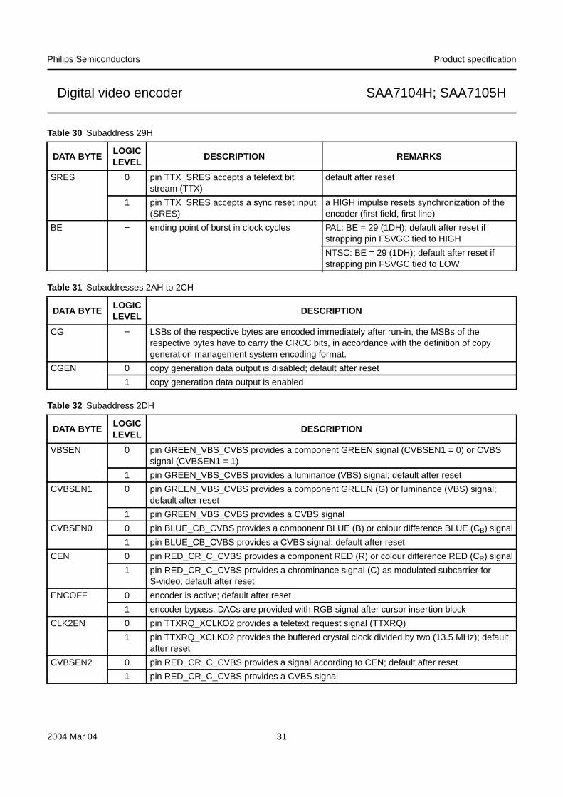
Philips Semiconductors Product specification
Digital video encoder SAA7104H; SAA7105H
Table 30 Subaddress 29H
Table 31 Subaddresses 2AH to 2CH
Table 32 Subaddress 2DH
DATA BYTELOGICLEVEL
DESCRIPTION REMARKS
SRES 0 pin TTX_SRES accepts a teletext bitstream (TTX)
default after reset
1 pin TTX_SRES accepts a sync reset input(SRES)
a HIGH impulse resets synchronization of theencoder (first field, first line)
BE − ending point of burst in clock cycles PAL: BE = 29 (1DH); default after reset ifstrapping pin FSVGC tied to HIGH
NTSC: BE = 29 (1DH); default after reset ifstrapping pin FSVGC tied to LOW
DATA BYTELOGICLEVEL
DESCRIPTION
CG − LSBs of the respective bytes are encoded immediately after run-in, the MSBs of therespective bytes have to carry the CRCC bits, in accordance with the definition of copygeneration management system encoding format.
CGEN 0 copy generation data output is disabled; default after reset
1 copy generation data output is enabled
DATA BYTELOGICLEVEL
DESCRIPTION
VBSEN 0 pin GREEN_VBS_CVBS provides a component GREEN signal (CVBSEN1 = 0) or CVBSsignal (CVBSEN1 = 1)
1 pin GREEN_VBS_CVBS provides a luminance (VBS) signal; default after reset
CVBSEN1 0 pin GREEN_VBS_CVBS provides a component GREEN (G) or luminance (VBS) signal;default after reset
1 pin GREEN_VBS_CVBS provides a CVBS signal
CVBSEN0 0 pin BLUE_CB_CVBS provides a component BLUE (B) or colour difference BLUE (CB) signal
1 pin BLUE_CB_CVBS provides a CVBS signal; default after reset
CEN 0 pin RED_CR_C_CVBS provides a component RED (R) or colour difference RED (CR) signal
1 pin RED_CR_C_CVBS provides a chrominance signal (C) as modulated subcarrier forS-video; default after reset
ENCOFF 0 encoder is active; default after reset
1 encoder bypass, DACs are provided with RGB signal after cursor insertion block
CLK2EN 0 pin TTXRQ_XCLKO2 provides a teletext request signal (TTXRQ)
1 pin TTXRQ_XCLKO2 provides the buffered crystal clock divided by two (13.5 MHz); defaultafter reset
CVBSEN2 0 pin RED_CR_C_CVBS provides a signal according to CEN; default after reset
1 pin RED_CR_C_CVBS provides a CVBS signal
2004 Mar 04 31
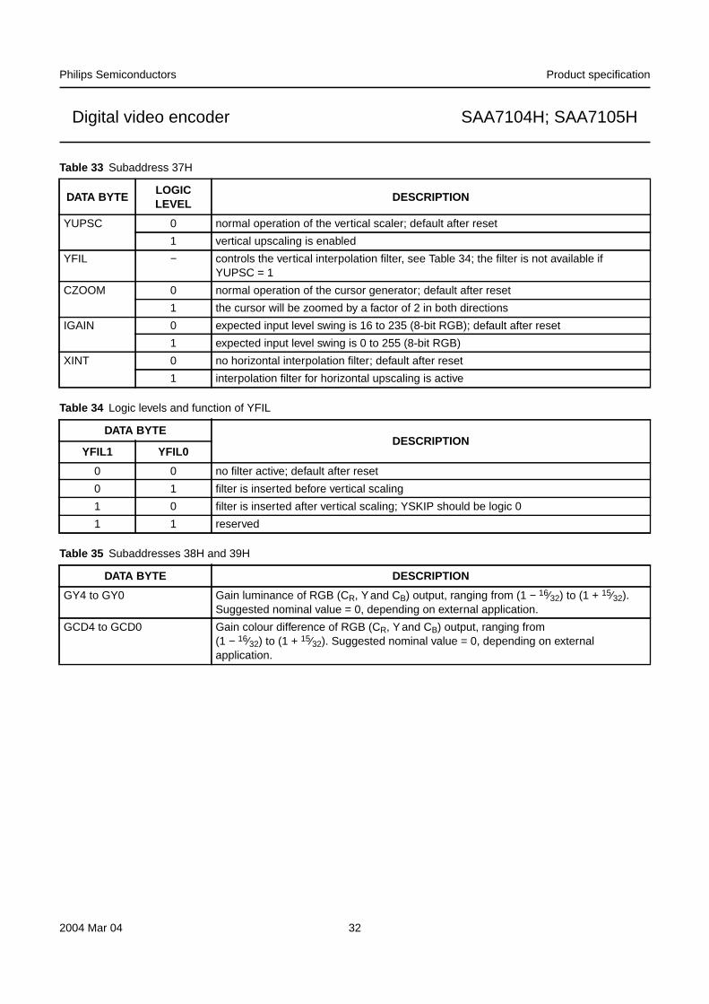
Philips Semiconductors Product specification
Digital video encoder SAA7104H; SAA7105H
Table 33 Subaddress 37H
Table 34 Logic levels and function of YFIL
Table 35 Subaddresses 38H and 39H
DATA BYTELOGICLEVEL
DESCRIPTION
YUPSC 0 normal operation of the vertical scaler; default after reset
1 vertical upscaling is enabled
YFIL − controls the vertical interpolation filter, see Table 34; the filter is not available ifYUPSC = 1
CZOOM 0 normal operation of the cursor generator; default after reset
1 the cursor will be zoomed by a factor of 2 in both directions
IGAIN 0 expected input level swing is 16 to 235 (8-bit RGB); default after reset
1 expected input level swing is 0 to 255 (8-bit RGB)
XINT 0 no horizontal interpolation filter; default after reset
1 interpolation filter for horizontal upscaling is active
DATA BYTEDESCRIPTION
YFIL1 YFIL0
0 0 no filter active; default after reset
0 1 filter is inserted before vertical scaling
1 0 filter is inserted after vertical scaling; YSKIP should be logic 0
1 1 reserved
DATA BYTE DESCRIPTION
GY4 to GY0 Gain luminance of RGB (CR, Yand CB) output, ranging from (1 − 16⁄32) to (1 + 15⁄32).Suggested nominal value = 0, depending on external application.
GCD4 to GCD0 Gain colour difference of RGB (CR, Yand CB) output, ranging from(1 − 16⁄32) to (1 + 15⁄32). Suggested nominal value = 0, depending on externalapplication.
2004 Mar 04 32
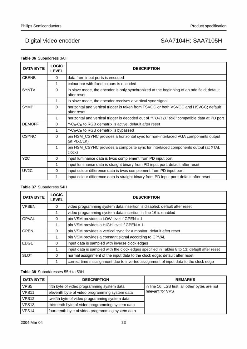
Philips Semiconductors Product specification
Digital video encoder SAA7104H; SAA7105H
Table 36 Subaddress 3AH
Table 37 Subaddress 54H
Table 38 Subaddresses 55H to 59H
DATA BYTELOGICLEVEL
DESCRIPTION
CBENB 0 data from input ports is encoded
1 colour bar with fixed colours is encoded
SYNTV 0 in slave mode, the encoder is only synchronized at the beginning of an odd field; defaultafter reset
1 in slave mode, the encoder receives a vertical sync signal
SYMP 0 horizontal and vertical trigger is taken from FSVGC or both VSVGC and HSVGC; defaultafter reset
1 horizontal and vertical trigger is decoded out of “ITU-R BT.656” compatible data at PD port
DEMOFF 0 Y-CB-CR to RGB dematrix is active; default after reset
1 Y-CB-CR to RGB dematrix is bypassed
CSYNC 0 pin HSM_CSYNC provides a horizontal sync for non-interlaced VGA components output(at PIXCLK)
1 pin HSM_CSYNC provides a composite sync for interlaced components output (at XTALclock)
Y2C 0 input luminance data is twos complement from PD input port
1 input luminance data is straight binary from PD input port; default after reset
UV2C 0 input colour difference data is twos complement from PD input port
1 input colour difference data is straight binary from PD input port; default after reset
DATA BYTELOGICLEVEL
DESCRIPTION
VPSEN 0 video programming system data insertion is disabled; default after reset
1 video programming system data insertion in line 16 is enabled
GPVAL 0 pin VSM provides a LOW level if GPEN = 1
1 pin VSM provides a HIGH level if GPEN = 1
GPEN 0 pin VSM provides a vertical sync for a monitor; default after reset
1 pin VSM provides a constant signal according to GPVAL
EDGE 0 input data is sampled with inverse clock edges
1 input data is sampled with the clock edges specified in Tables 8 to 13; default after reset
SLOT 0 normal assignment of the input data to the clock edge; default after reset
1 correct time misalignment due to inverted assignment of input data to the clock edge
DATA BYTE DESCRIPTION REMARKS
VPS5 fifth byte of video programming system data in line 16; LSB first; all other bytes are notrelevant for VPSVPS11 eleventh byte of video programming system data
VPS12 twelfth byte of video programming system data
VPS13 thirteenth byte of video programming system data
VPS14 fourteenth byte of video programming system data
2004 Mar 04 33
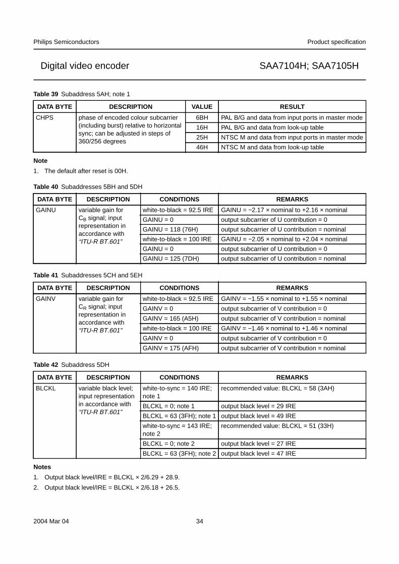
Philips Semiconductors Product specification
Digital video encoder SAA7104H; SAA7105H
Table 39 Subaddress 5AH; note 1
Note
1. The default after reset is 00H.
Table 40 Subaddresses 5BH and 5DH
Table 41 Subaddresses 5CH and 5EH
Table 42 Subaddress 5DH
Notes
1. Output black level/IRE = BLCKL × 2/6.29 + 28.9.
2. Output black level/IRE = BLCKL × 2/6.18 + 26.5.
DATA BYTE DESCRIPTION VALUE RESULT
CHPS phase of encoded colour subcarrier(including burst) relative to horizontalsync; can be adjusted in steps of360/256 degrees
6BH PAL B/G and data from input ports in master mode
16H PAL B/G and data from look-up table
25H NTSC M and data from input ports in master mode
46H NTSC M and data from look-up table
DATA BYTE DESCRIPTION CONDITIONS REMARKS
GAINU variable gain forCB signal; inputrepresentation inaccordance with“ITU-R BT.601”
white-to-black = 92.5 IRE GAINU = −2.17 × nominal to +2.16 × nominal
GAINU = 0 output subcarrier of U contribution = 0
GAINU = 118 (76H) output subcarrier of U contribution = nominal
white-to-black = 100 IRE GAINU = −2.05 × nominal to +2.04 × nominal
GAINU = 0 output subcarrier of U contribution = 0
GAINU = 125 (7DH) output subcarrier of U contribution = nominal
DATA BYTE DESCRIPTION CONDITIONS REMARKS
GAINV variable gain forCR signal; inputrepresentation inaccordance with“ITU-R BT.601”
white-to-black = 92.5 IRE GAINV = −1.55 × nominal to +1.55 × nominal
GAINV = 0 output subcarrier of V contribution = 0
GAINV = 165 (A5H) output subcarrier of V contribution = nominal
white-to-black = 100 IRE GAINV = −1.46 × nominal to +1.46 × nominal
GAINV = 0 output subcarrier of V contribution = 0
GAINV = 175 (AFH) output subcarrier of V contribution = nominal
DATA BYTE DESCRIPTION CONDITIONS REMARKS
BLCKL variable black level;input representationin accordance with“ITU-R BT.601”
white-to-sync = 140 IRE;note 1
recommended value: BLCKL = 58 (3AH)
BLCKL = 0; note 1 output black level = 29 IRE
BLCKL = 63 (3FH); note 1 output black level = 49 IRE
white-to-sync = 143 IRE;note 2
recommended value: BLCKL = 51 (33H)
BLCKL = 0; note 2 output black level = 27 IRE
BLCKL = 63 (3FH); note 2 output black level = 47 IRE
2004 Mar 04 34
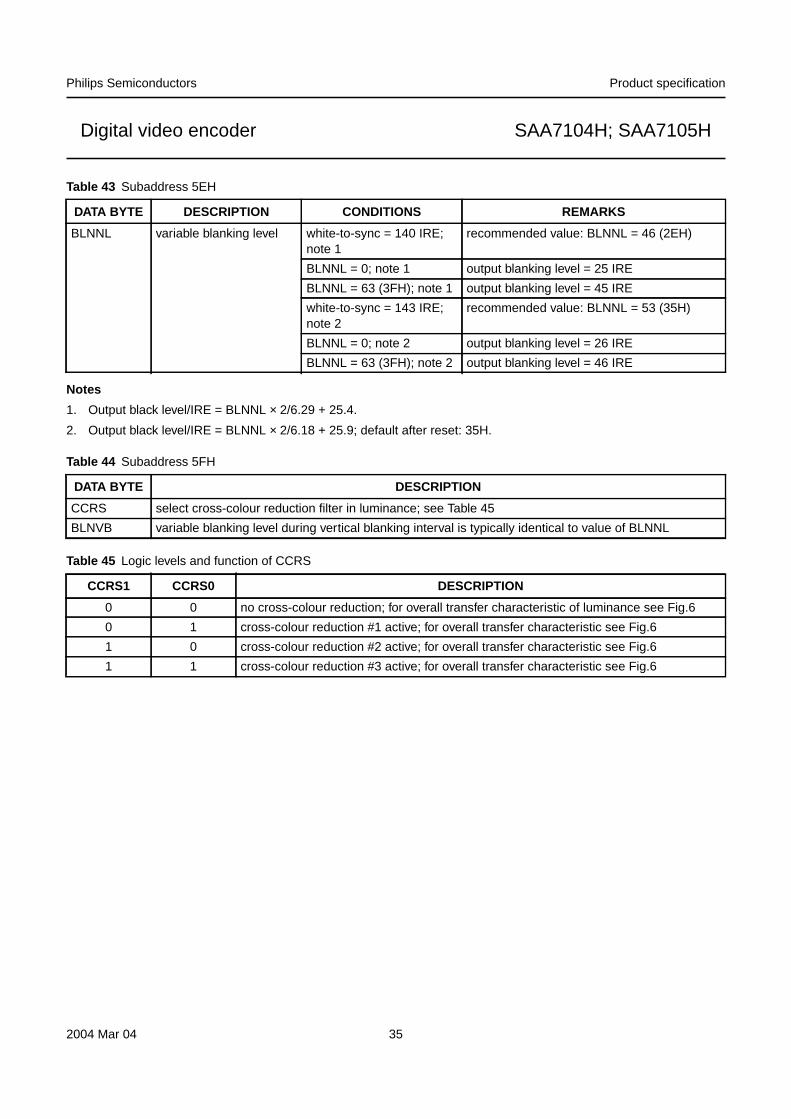
Philips Semiconductors Product specification
Digital video encoder SAA7104H; SAA7105H
Table 43 Subaddress 5EH
Notes
1. Output black level/IRE = BLNNL × 2/6.29 + 25.4.
2. Output black level/IRE = BLNNL × 2/6.18 + 25.9; default after reset: 35H.
Table 44 Subaddress 5FH
Table 45 Logic levels and function of CCRS
DATA BYTE DESCRIPTION CONDITIONS REMARKS
BLNNL variable blanking level white-to-sync = 140 IRE;note 1
recommended value: BLNNL = 46 (2EH)
BLNNL = 0; note 1 output blanking level = 25 IRE
BLNNL = 63 (3FH); note 1 output blanking level = 45 IRE
white-to-sync = 143 IRE;note 2
recommended value: BLNNL = 53 (35H)
BLNNL = 0; note 2 output blanking level = 26 IRE
BLNNL = 63 (3FH); note 2 output blanking level = 46 IRE
DATA BYTE DESCRIPTION
CCRS select cross-colour reduction filter in luminance; see Table 45
BLNVB variable blanking level during vertical blanking interval is typically identical to value of BLNNL
CCRS1 CCRS0 DESCRIPTION
0 0 no cross-colour reduction; for overall transfer characteristic of luminance see Fig.6
0 1 cross-colour reduction #1 active; for overall transfer characteristic see Fig.6
1 0 cross-colour reduction #2 active; for overall transfer characteristic see Fig.6
1 1 cross-colour reduction #3 active; for overall transfer characteristic see Fig.6
2004 Mar 04 35
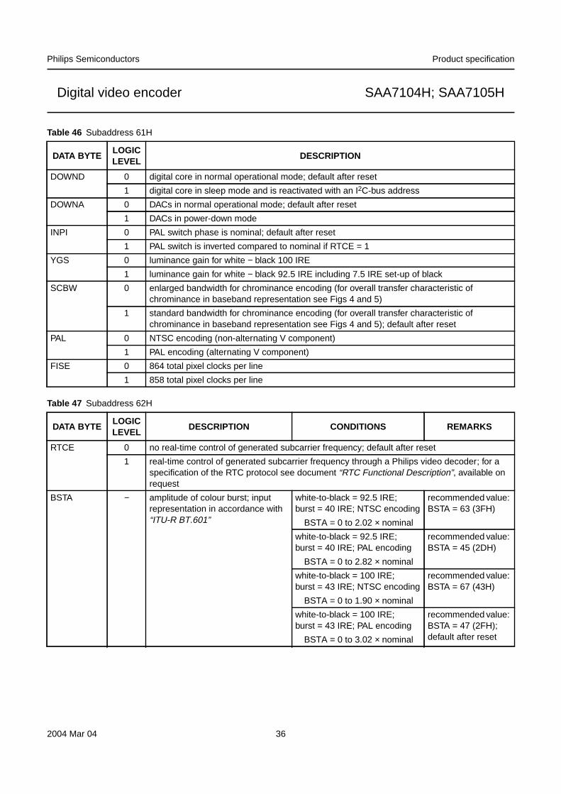
Philips Semiconductors Product specification
Digital video encoder SAA7104H; SAA7105H
Table 46 Subaddress 61H
Table 47 Subaddress 62H
DATA BYTELOGICLEVEL
DESCRIPTION
DOWND 0 digital core in normal operational mode; default after reset
1 digital core in sleep mode and is reactivated with an I2C-bus address
DOWNA 0 DACs in normal operational mode; default after reset
1 DACs in power-down mode
INPI 0 PAL switch phase is nominal; default after reset
1 PAL switch is inverted compared to nominal if RTCE = 1
YGS 0 luminance gain for white − black 100 IRE
1 luminance gain for white − black 92.5 IRE including 7.5 IRE set-up of black
SCBW 0 enlarged bandwidth for chrominance encoding (for overall transfer characteristic ofchrominance in baseband representation see Figs 4 and 5)
1 standard bandwidth for chrominance encoding (for overall transfer characteristic ofchrominance in baseband representation see Figs 4 and 5); default after reset
PAL 0 NTSC encoding (non-alternating V component)
1 PAL encoding (alternating V component)
FISE 0 864 total pixel clocks per line
1 858 total pixel clocks per line
DATA BYTELOGICLEVEL
DESCRIPTION CONDITIONS REMARKS
RTCE 0 no real-time control of generated subcarrier frequency; default after reset
1 real-time control of generated subcarrier frequency through a Philips video decoder; for aspecification of the RTC protocol see document “RTC Functional Description”, available onrequest
BSTA − amplitude of colour burst; inputrepresentation in accordance with“ITU-R BT.601”
white-to-black = 92.5 IRE;burst = 40 IRE; NTSC encoding
recommended value:BSTA = 63 (3FH)
BSTA = 0 to 2.02 × nominal
white-to-black = 92.5 IRE;burst = 40 IRE; PAL encoding
recommended value:BSTA = 45 (2DH)
BSTA = 0 to 2.82 × nominal
white-to-black = 100 IRE;burst = 43 IRE; NTSC encoding
recommended value:BSTA = 67 (43H)
BSTA = 0 to 1.90 × nominal
white-to-black = 100 IRE;burst = 43 IRE; PAL encoding
recommended value:BSTA = 47 (2FH);default after resetBSTA = 0 to 3.02 × nominal
2004 Mar 04 36
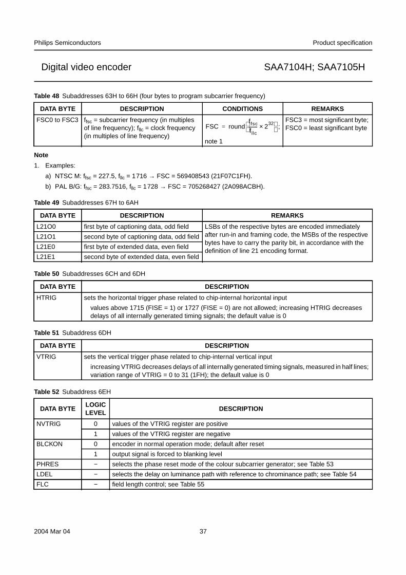
Philips Semiconductors Product specification
Digital video encoder SAA7104H; SAA7105H
Table 48 Subaddresses 63H to 66H (four bytes to program subcarrier frequency)
Note
1. Examples:
a) NTSC M: ffsc = 227.5, fllc = 1716 → FSC = 569408543 (21F07C1FH).
b) PAL B/G: ffsc = 283.7516, fllc = 1728 → FSC = 705268427 (2A098ACBH).
Table 49 Subaddresses 67H to 6AH
Table 50 Subaddresses 6CH and 6DH
Table 51 Subaddress 6DH
Table 52 Subaddress 6EH
DATA BYTE DESCRIPTION CONDITIONS REMARKS
FSC0 to FSC3 ffsc = subcarrier frequency (in multiplesof line frequency); fllc = clock frequency(in multiples of line frequency)
;
note 1
FSC3 = most significant byte;FSC0 = least significant byte
DATA BYTE DESCRIPTION REMARKS
L21O0 first byte of captioning data, odd field LSBs of the respective bytes are encoded immediatelyafter run-in and framing code, the MSBs of the respectivebytes have to carry the parity bit, in accordance with thedefinition of line 21 encoding format.
L21O1 second byte of captioning data, odd field
L21E0 first byte of extended data, even field
L21E1 second byte of extended data, even field
DATA BYTE DESCRIPTION
HTRIG sets the horizontal trigger phase related to chip-internal horizontal input
values above 1715 (FISE = 1) or 1727 (FISE = 0) are not allowed; increasing HTRIG decreasesdelays of all internally generated timing signals; the default value is 0
DATA BYTE DESCRIPTION
VTRIG sets the vertical trigger phase related to chip-internal vertical input
increasing VTRIG decreases delays of all internally generated timing signals, measured in half lines;variation range of VTRIG = 0 to 31 (1FH); the default value is 0
DATA BYTELOGICLEVEL
DESCRIPTION
NVTRIG 0 values of the VTRIG register are positive
1 values of the VTRIG register are negative
BLCKON 0 encoder in normal operation mode; default after reset
1 output signal is forced to blanking level
PHRES − selects the phase reset mode of the colour subcarrier generator; see Table 53
LDEL − selects the delay on luminance path with reference to chrominance path; see Table 54
FLC − field length control; see Table 55
FSC roundffsc
fllc-------- 232×
=
2004 Mar 04 37
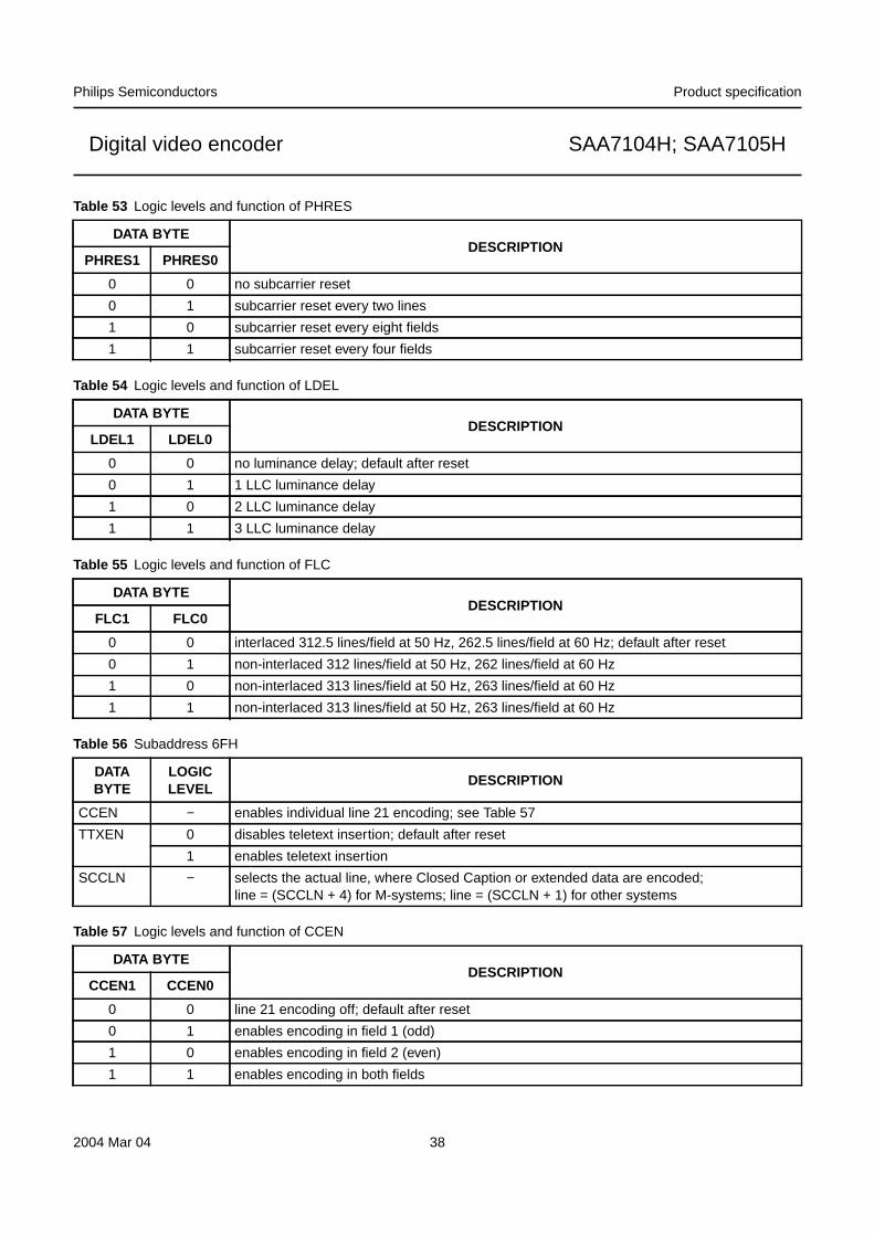
Philips Semiconductors Product specification
Digital video encoder SAA7104H; SAA7105H
Table 53 Logic levels and function of PHRES
Table 54 Logic levels and function of LDEL
Table 55 Logic levels and function of FLC
Table 56 Subaddress 6FH
Table 57 Logic levels and function of CCEN
DATA BYTEDESCRIPTION
PHRES1 PHRES0
0 0 no subcarrier reset
0 1 subcarrier reset every two lines
1 0 subcarrier reset every eight fields
1 1 subcarrier reset every four fields
DATA BYTEDESCRIPTION
LDEL1 LDEL0
0 0 no luminance delay; default after reset
0 1 1 LLC luminance delay
1 0 2 LLC luminance delay
1 1 3 LLC luminance delay
DATA BYTEDESCRIPTION
FLC1 FLC0
0 0 interlaced 312.5 lines/field at 50 Hz, 262.5 lines/field at 60 Hz; default after reset
0 1 non-interlaced 312 lines/field at 50 Hz, 262 lines/field at 60 Hz
1 0 non-interlaced 313 lines/field at 50 Hz, 263 lines/field at 60 Hz
1 1 non-interlaced 313 lines/field at 50 Hz, 263 lines/field at 60 Hz
DATABYTE
LOGICLEVEL
DESCRIPTION
CCEN − enables individual line 21 encoding; see Table 57
TTXEN 0 disables teletext insertion; default after reset
1 enables teletext insertion
SCCLN − selects the actual line, where Closed Caption or extended data are encoded;line = (SCCLN + 4) for M-systems; line = (SCCLN + 1) for other systems
DATA BYTEDESCRIPTION
CCEN1 CCEN0
0 0 line 21 encoding off; default after reset
0 1 enables encoding in field 1 (odd)
1 0 enables encoding in field 2 (even)
1 1 enables encoding in both fields
2004 Mar 04 38
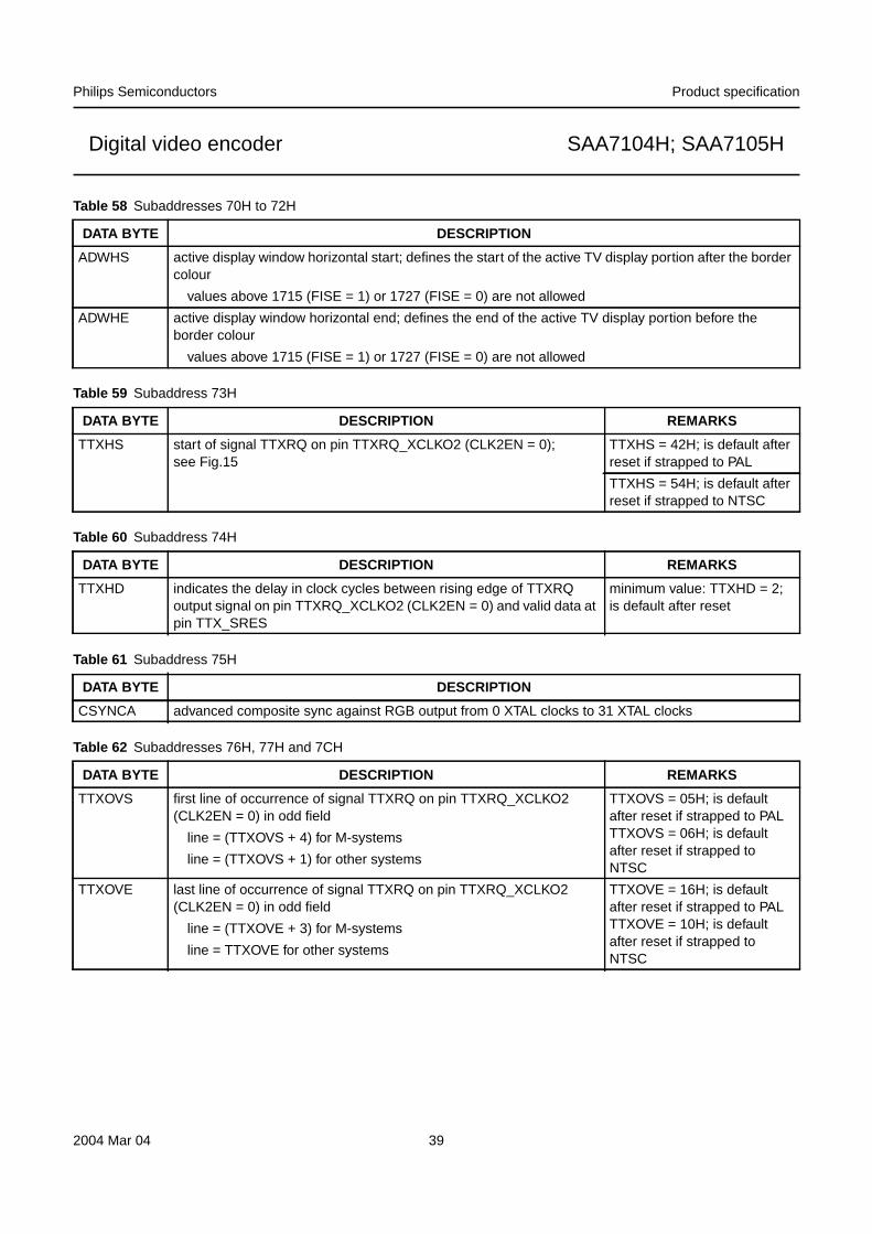
Philips Semiconductors Product specification
Digital video encoder SAA7104H; SAA7105H
Table 58 Subaddresses 70H to 72H
Table 59 Subaddress 73H
Table 60 Subaddress 74H
Table 61 Subaddress 75H
Table 62 Subaddresses 76H, 77H and 7CH
DATA BYTE DESCRIPTION
ADWHS active display window horizontal start; defines the start of the active TV display portion after the bordercolour
values above 1715 (FISE = 1) or 1727 (FISE = 0) are not allowed
ADWHE active display window horizontal end; defines the end of the active TV display portion before theborder colour
values above 1715 (FISE = 1) or 1727 (FISE = 0) are not allowed
DATA BYTE DESCRIPTION REMARKS
TTXHS start of signal TTXRQ on pin TTXRQ_XCLKO2 (CLK2EN = 0);see Fig.15
TTXHS = 42H; is default afterreset if strapped to PAL
TTXHS = 54H; is default afterreset if strapped to NTSC
DATA BYTE DESCRIPTION REMARKS
TTXHD indicates the delay in clock cycles between rising edge of TTXRQoutput signal on pin TTXRQ_XCLKO2 (CLK2EN = 0) and valid data atpin TTX_SRES
minimum value: TTXHD = 2;is default after reset
DATA BYTE DESCRIPTION
CSYNCA advanced composite sync against RGB output from 0 XTAL clocks to 31 XTAL clocks
DATA BYTE DESCRIPTION REMARKS
TTXOVS first line of occurrence of signal TTXRQ on pin TTXRQ_XCLKO2(CLK2EN = 0) in odd field
TTXOVS = 05H; is defaultafter reset if strapped to PALTTXOVS = 06H; is defaultafter reset if strapped toNTSC
line = (TTXOVS + 4) for M-systems
line = (TTXOVS + 1) for other systems
TTXOVE last line of occurrence of signal TTXRQ on pin TTXRQ_XCLKO2(CLK2EN = 0) in odd field
TTXOVE = 16H; is defaultafter reset if strapped to PALTTXOVE = 10H; is defaultafter reset if strapped toNTSC
line = (TTXOVE + 3) for M-systems
line = TTXOVE for other systems
2004 Mar 04 39
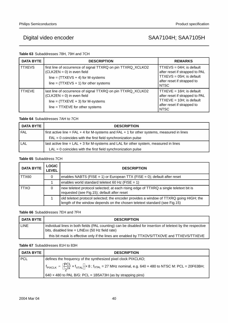
Philips Semiconductors Product specification
Digital video encoder SAA7104H; SAA7105H
Table 63 Subaddresses 78H, 79H and 7CH
Table 64 Subaddresses 7AH to 7CH
Table 65 Subaddress 7CH
Table 66 Subaddresses 7EH and 7FH
Table 67 Subaddresses 81H to 83H
DATA BYTE DESCRIPTION REMARKS
TTXEVS first line of occurrence of signal TTXRQ on pin TTXRQ_XCLKO2(CLK2EN = 0) in even field
TTXEVS = 04H; is defaultafter reset if strapped to PALTTXEVS = 05H; is defaultafter reset if strapped toNTSC
line = (TTXEVS + 4) for M-systems
line = (TTXEVS + 1) for other systems
TTXEVE last line of occurrence of signal TTXRQ on pin TTXRQ_XCLKO2(CLK2EN = 0) in even field
TTXEVE = 16H; is defaultafter reset if strapped to PALTTXEVE = 10H; is defaultafter reset if strapped toNTSC
line = (TTXEVE + 3) for M-systems
line = TTXEVE for other systems
DATA BYTE DESCRIPTION
FAL first active line = FAL + 4 for M-systems and FAL + 1 for other systems, measured in lines
FAL = 0 coincides with the first field synchronization pulse
LAL last active line = LAL + 3 for M-systems and LAL for other system, measured in lines
LAL = 0 coincides with the first field synchronization pulse
DATA BYTELOGICLEVEL
DESCRIPTION
TTX60 0 enables NABTS (FISE = 1) or European TTX (FISE = 0); default after reset
1 enables world standard teletext 60 Hz (FISE = 1)
TTXO 0 new teletext protocol selected; at each rising edge of TTXRQ a single teletext bit isrequested (see Fig.15); default after reset
1 old teletext protocol selected; the encoder provides a window of TTXRQ going HIGH; thelength of the window depends on the chosen teletext standard (see Fig.15)
DATA BYTE DESCRIPTION
LINE individual lines in both fields (PAL counting) can be disabled for insertion of teletext by the respectivebits, disabled line = LINExx (50 Hz field rate)
this bit mask is effective only if the lines are enabled by TTXOVS/TTXOVE and TTXEVS/TTXEVE
DATA BYTE DESCRIPTION
PCL defines the frequency of the synthesized pixel clock PIXCLKO;
; fXTAL = 27 MHz nominal, e.g. 640 × 480 to NTSC M: PCL = 20F63BH;
640 × 480 to PAL B/G: PCL = 1B5A73H (as by strapping pins)
fPIXCLKPCL
224----------- fXTAL×
8×=
2004 Mar 04 40
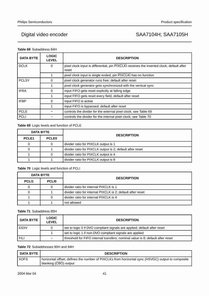
Philips Semiconductors Product specification
Digital video encoder SAA7104H; SAA7105H
Table 68 Subaddress 84H
Table 69 Logic levels and function of PCLE
Table 70 Logic levels and function of PCLI
Table 71 Subaddress 85H
Table 72 Subaddresses 90H and 94H
DATA BYTELOGICLEVEL
DESCRIPTION
DCLK 0 pixel clock input is differential, pin PIXCLKI receives the inverted clock; default afterreset
1 pixel clock input is single ended, pin PIXCLKI has no function
PCLSY 0 pixel clock generator runs free; default after reset
1 pixel clock generator gets synchronized with the vertical sync
IFRA 0 input FIFO gets reset explicitly at falling edge
1 input FIFO gets reset every field; default after reset
IFBP 0 input FIFO is active
1 input FIFO is bypassed; default after reset
PCLE − controls the divider for the external pixel clock; see Table 69
PCLI − controls the divider for the internal pixel clock; see Table 70
DATA BYTEDESCRIPTION
PCLE1 PCLE0
0 0 divider ratio for PIXCLK output is 1
0 1 divider ratio for PIXCLK output is 2; default after reset
1 0 divider ratio for PIXCLK output is 4
1 1 divider ratio for PIXCLK output is 8
DATA BYTEDESCRIPTION
PCLI1 PCLI0
0 0 divider ratio for internal PIXCLK is 1
0 1 divider ratio for internal PIXCLK is 2; default after reset
1 0 divider ratio for internal PIXCLK is 4
1 1 not allowed
DATA BYTELOGICLEVEL
DESCRIPTION
EIDIV 0 set to logic 0 if DVO compliant signals are applied; default after reset
1 set to logic 1 if non-DVO compliant signals are applied
FILI − threshold for FIFO internal transfers; nominal value is 8; default after reset
DATA BYTE DESCRIPTION
XOFS horizontal offset; defines the number of PIXCLKs from horizontal sync (HSVGC) output to compositeblanking (CBO) output
2004 Mar 04 41
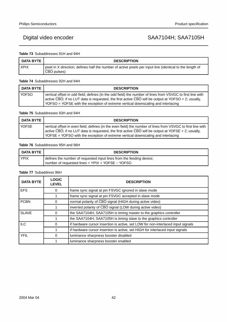
Philips Semiconductors Product specification
Digital video encoder SAA7104H; SAA7105H
Table 73 Subaddresses 91H and 94H
Table 74 Subaddresses 92H and 94H
Table 75 Subaddresses 93H and 94H
Table 76 Subaddresses 95H and 96H
Table 77 Subaddress 96H
DATA BYTE DESCRIPTION
XPIX pixel in X direction; defines half the number of active pixels per input line (identical to the length ofCBO pulses)
DATA BYTE DESCRIPTION
YOFSO vertical offset in odd field; defines (in the odd field) the number of lines from VSVGC to first line withactive CBO; if no LUT data is requested, the first active CBO will be output at YOFSO + 2; usually,YOFSO = YOFSE with the exception of extreme vertical downscaling and interlacing
DATA BYTE DESCRIPTION
YOFSE vertical offset in even field; defines (in the even field) the number of lines from VSVGC to first line withactive CBO; if no LUT data is requested, the first active CBO will be output at YOFSE + 2; usually,YOFSE = YOFSO with the exception of extreme vertical downscaling and interlacing
DATA BYTE DESCRIPTION
YPIX defines the number of requested input lines from the feeding device;number of requested lines = YPIX + YOFSE − YOFSO
DATA BYTELOGICLEVEL
DESCRIPTION
EFS 0 frame sync signal at pin FSVGC ignored in slave mode
1 frame sync signal at pin FSVGC accepted in slave mode
PCBN 0 normal polarity of CBO signal (HIGH during active video)
1 inverted polarity of CBO signal (LOW during active video)
SLAVE 0 the SAA7104H; SAA7105H is timing master to the graphics controller
1 the SAA7104H; SAA7105H is timing slave to the graphics controller
ILC 0 if hardware cursor insertion is active, set LOW for non-interlaced input signals
1 if hardware cursor insertion is active, set HIGH for interlaced input signals
YFIL 0 luminance sharpness booster disabled
1 luminance sharpness booster enabled
2004 Mar 04 42
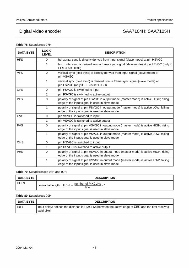
Philips Semiconductors Product specification
Digital video encoder SAA7104H; SAA7105H
Table 78 Subaddress 97H
Table 79 Subaddresses 98H and 99H
Table 80 Subaddress 99H
DATA BYTELOGICLEVEL
DESCRIPTION
HFS 0 horizontal sync is directly derived from input signal (slave mode) at pin HSVGC
1 horizontal sync is derived from a frame sync signal (slave mode) at pin FSVGC (only ifEFS is set HIGH)
VFS 0 vertical sync (field sync) is directly derived from input signal (slave mode) atpin VSVGC
1 vertical sync (field sync) is derived from a frame sync signal (slave mode) atpin FSVGC (only if EFS is set HIGH)
OFS 0 pin FSVGC is switched to input
1 pin FSVGC is switched to active output
PFS 0 polarity of signal at pin FSVGC in output mode (master mode) is active HIGH; risingedge of the input signal is used in slave mode
1 polarity of signal at pin FSVGC in output mode (master mode) is active LOW; fallingedge of the input signal is used in slave mode
OVS 0 pin VSVGC is switched to input
1 pin VSVGC is switched to active output
PVS 0 polarity of signal at pin VSVGC in output mode (master mode) is active HIGH; risingedge of the input signal is used in slave mode
1 polarity of signal at pin VSVGC in output mode (master mode) is active LOW; fallingedge of the input signal is used in slave mode
OHS 0 pin HSVGC is switched to input
1 pin HSVGC is switched to active output
PHS 0 polarity of signal at pin HSVGC in output mode (master mode) is active HIGH; risingedge of the input signal is used in slave mode
1 polarity of signal at pin HSVGC in output mode (master mode) is active LOW; fallingedge of the input signal is used in slave mode
DATA BYTE DESCRIPTION
HLENhorizontal length;
DATA BYTE DESCRIPTION
IDEL input delay; defines the distance in PIXCLKs between the active edge of CBO and the first receivedvalid pixel
HLEN number of PIXCLKsline
----------------------------------------------------- 1–=
2004 Mar 04 43
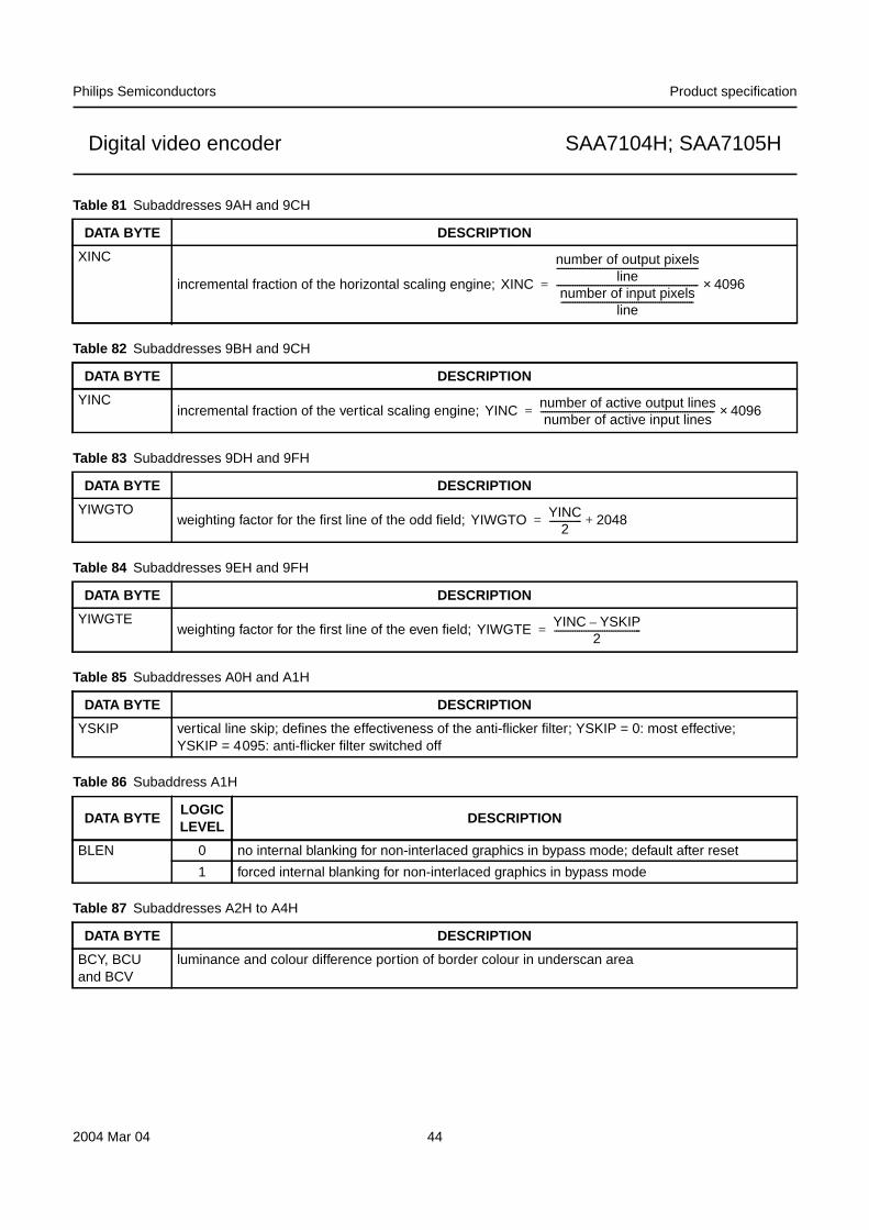
Philips Semiconductors Product specification
Digital video encoder SAA7104H; SAA7105H
Table 81 Subaddresses 9AH and 9CH
Table 82 Subaddresses 9BH and 9CH
Table 83 Subaddresses 9DH and 9FH
Table 84 Subaddresses 9EH and 9FH
Table 85 Subaddresses A0H and A1H
Table 86 Subaddress A1H
Table 87 Subaddresses A2H to A4H
DATA BYTE DESCRIPTION
XINC
incremental fraction of the horizontal scaling engine;
DATA BYTE DESCRIPTION
YINCincremental fraction of the vertical scaling engine;
DATA BYTE DESCRIPTION
YIWGTOweighting factor for the first line of the odd field;
DATA BYTE DESCRIPTION
YIWGTEweighting factor for the first line of the even field;
DATA BYTE DESCRIPTION
YSKIP vertical line skip; defines the effectiveness of the anti-flicker filter; YSKIP = 0: most effective;YSKIP = 4095: anti-flicker filter switched off
DATA BYTELOGICLEVEL
DESCRIPTION
BLEN 0 no internal blanking for non-interlaced graphics in bypass mode; default after reset
1 forced internal blanking for non-interlaced graphics in bypass mode
DATA BYTE DESCRIPTION
BCY, BCUand BCV
luminance and colour difference portion of border colour in underscan area
XINC
number of output pixelsline
--------------------------------------------------------------
number of input pixelsline
------------------------------------------------------------------------------------------------------------------------ 4096×=
YINC number of active output linesnumber of active input lines
---------------------------------------------------------------------------- 4096×=
YIWGTO YINC2
-------------- 2048+=
YIWGTE YINC YSKIP–2
--------------------------------------=
2004 Mar 04 44
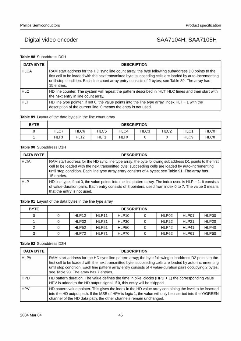
Philips Semiconductors Product specification
Digital video encoder SAA7104H; SAA7105H
Table 88 Subaddress D0H
Table 89 Layout of the data bytes in the line count array
Table 90 Subaddress D1H
Table 91 Layout of the data bytes in the line type array
Table 92 Subaddress D2H
DATA BYTE DESCRIPTION
HLCA RAM start address for the HD sync line count array; the byte following subaddress D0 points to thefirst cell to be loaded with the next transmitted byte; succeeding cells are loaded by auto-incrementinguntil stop condition. Each line count array entry consists of 2 bytes; see Table 89. The array has15 entries.
HLC HD line counter. The system will repeat the pattern described in ‘HLT’ HLC times and then start withthe next entry in line count array.
HLT HD line type pointer. If not 0, the value points into the line type array, index HLT − 1 with thedescription of the current line. 0 means the entry is not used.
BYTE DESCRIPTION
0 HLC7 HLC6 HLC5 HLC4 HLC3 HLC2 HLC1 HLC0
1 HLT3 HLT2 HLT1 HLT0 0 0 HLC9 HLC8
DATA BYTE DESCRIPTION
HLTA RAM start address for the HD sync line type array; the byte following subaddress D1 points to the firstcell to be loaded with the next transmitted byte; succeeding cells are loaded by auto-incrementinguntil stop condition. Each line type array entry consists of 4 bytes; see Table 91. The array has15 entries.
HLP HD line type; if not 0, the value points into the line pattern array. The index used is HLP − 1. It consistsof value-duration pairs. Each entry consists of 8 pointers, used from index 0 to 7. The value 0 meansthat the entry is not used.
BYTE DESCRIPTION
0 0 HLP12 HLP11 HLP10 0 HLP02 HLP01 HLP00
1 0 HLP32 HLP31 HLP30 0 HLP22 HLP21 HLP20
2 0 HLP52 HLP51 HLP50 0 HLP42 HLP41 HLP40
3 0 HLP72 HLP71 HLP70 0 HLP62 HLP61 HLP60
DATA BYTE DESCRIPTION
HLPA RAM start address for the HD sync line pattern array; the byte following subaddress D2 points to thefirst cell to be loaded with the next transmitted byte; succeeding cells are loaded by auto-incrementinguntil stop condition. Each line pattern array entry consists of 4 value-duration pairs occupying 2 bytes;see Table 93. The array has 7 entries.
HPD HD pattern duration. The value defines the time in pixel clocks (HPD + 1) the corresponding valueHPV is added to the HD output signal. If 0, this entry will be skipped.
HPV HD pattern value pointer. This gives the index in the HD value array containing the level to be insertedinto the HD output path. If the MSB of HPV is logic 1, the value will only be inserted into the Y/GREENchannel of the HD data path, the other channels remain unchanged.
2004 Mar 04 45
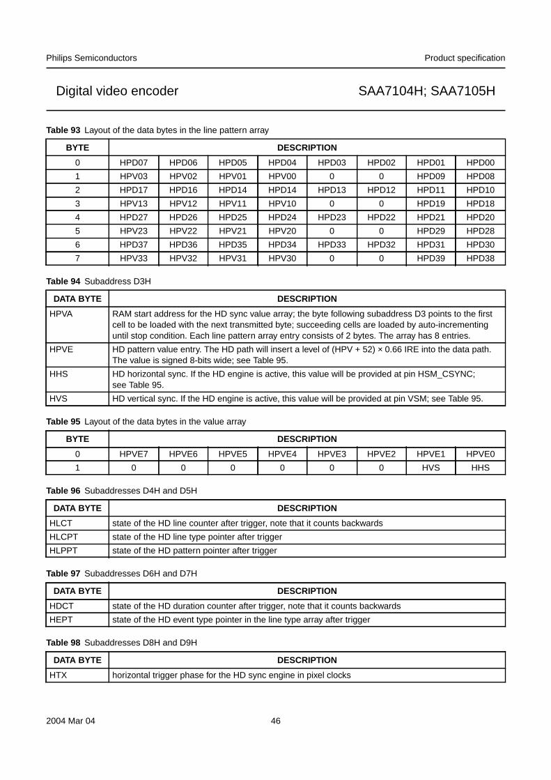
Philips Semiconductors Product specification
Digital video encoder SAA7104H; SAA7105H
Table 93 Layout of the data bytes in the line pattern array
Table 94 Subaddress D3H
Table 95 Layout of the data bytes in the value array
Table 96 Subaddresses D4H and D5H
Table 97 Subaddresses D6H and D7H
Table 98 Subaddresses D8H and D9H
BYTE DESCRIPTION
0 HPD07 HPD06 HPD05 HPD04 HPD03 HPD02 HPD01 HPD00
1 HPV03 HPV02 HPV01 HPV00 0 0 HPD09 HPD08
2 HPD17 HPD16 HPD14 HPD14 HPD13 HPD12 HPD11 HPD10
3 HPV13 HPV12 HPV11 HPV10 0 0 HPD19 HPD18
4 HPD27 HPD26 HPD25 HPD24 HPD23 HPD22 HPD21 HPD20
5 HPV23 HPV22 HPV21 HPV20 0 0 HPD29 HPD28
6 HPD37 HPD36 HPD35 HPD34 HPD33 HPD32 HPD31 HPD30
7 HPV33 HPV32 HPV31 HPV30 0 0 HPD39 HPD38
DATA BYTE DESCRIPTION
HPVA RAM start address for the HD sync value array; the byte following subaddress D3 points to the firstcell to be loaded with the next transmitted byte; succeeding cells are loaded by auto-incrementinguntil stop condition. Each line pattern array entry consists of 2 bytes. The array has 8 entries.
HPVE HD pattern value entry. The HD path will insert a level of (HPV + 52) × 0.66 IRE into the data path.The value is signed 8-bits wide; see Table 95.
HHS HD horizontal sync. If the HD engine is active, this value will be provided at pin HSM_CSYNC;see Table 95.
HVS HD vertical sync. If the HD engine is active, this value will be provided at pin VSM; see Table 95.
BYTE DESCRIPTION
0 HPVE7 HPVE6 HPVE5 HPVE4 HPVE3 HPVE2 HPVE1 HPVE0
1 0 0 0 0 0 0 HVS HHS
DATA BYTE DESCRIPTION
HLCT state of the HD line counter after trigger, note that it counts backwards
HLCPT state of the HD line type pointer after trigger
HLPPT state of the HD pattern pointer after trigger
DATA BYTE DESCRIPTION
HDCT state of the HD duration counter after trigger, note that it counts backwards
HEPT state of the HD event type pointer in the line type array after trigger
DATA BYTE DESCRIPTION
HTX horizontal trigger phase for the HD sync engine in pixel clocks
2004 Mar 04 46
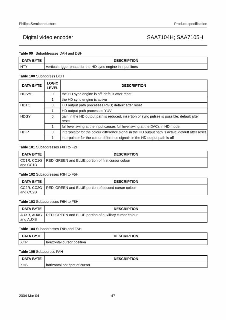
Philips Semiconductors Product specification
Digital video encoder SAA7104H; SAA7105H
Table 99 Subaddresses DAH and DBH
Table 100 Subaddress DCH
Table 101 Subaddresses F0H to F2H
Table 102 Subaddresses F3H to F5H
Table 103 Subaddresses F6H to F8H
Table 104 Subaddresses F9H and FAH
Table 105 Subaddress FAH
DATA BYTE DESCRIPTION
HTY vertical trigger phase for the HD sync engine in input lines
DATA BYTELOGICLEVEL
DESCRIPTION
HDSYE 0 the HD sync engine is off; default after reset
1 the HD sync engine is active
HDTC 0 HD output path processes RGB; default after reset
1 HD output path processes YUV
HDGY 0 gain in the HD output path is reduced, insertion of sync pulses is possible; default afterreset
1 full level swing at the input causes full level swing at the DACs in HD mode
HDIP 0 interpolator for the colour difference signal in the HD output path is active; default after reset
1 interpolator for the colour difference signals in the HD output path is off
DATA BYTE DESCRIPTION
CC1R, CC1Gand CC1B
RED, GREEN and BLUE portion of first cursor colour
DATA BYTE DESCRIPTION
CC2R, CC2Gand CC2B
RED, GREEN and BLUE portion of second cursor colour
DATA BYTE DESCRIPTION
AUXR, AUXGand AUXB
RED, GREEN and BLUE portion of auxiliary cursor colour
DATA BYTE DESCRIPTION
XCP horizontal cursor position
DATA BYTE DESCRIPTION
XHS horizontal hot spot of cursor
2004 Mar 04 47
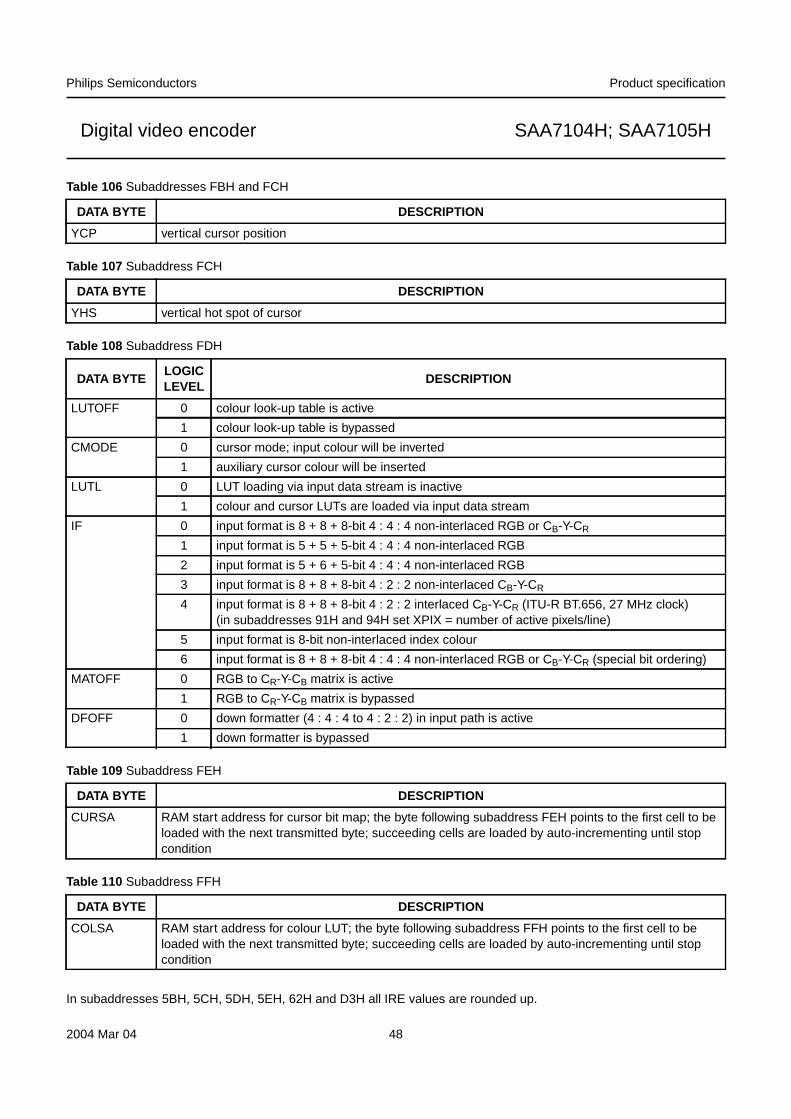
Philips Semiconductors Product specification
Digital video encoder SAA7104H; SAA7105H
Table 106 Subaddresses FBH and FCH
Table 107 Subaddress FCH
Table 108 Subaddress FDH
Table 109 Subaddress FEH
Table 110 Subaddress FFH
In subaddresses 5BH, 5CH, 5DH, 5EH, 62H and D3H all IRE values are rounded up.
DATA BYTE DESCRIPTION
YCP vertical cursor position
DATA BYTE DESCRIPTION
YHS vertical hot spot of cursor
DATA BYTELOGICLEVEL
DESCRIPTION
LUTOFF 0 colour look-up table is active
1 colour look-up table is bypassed
CMODE 0 cursor mode; input colour will be inverted
1 auxiliary cursor colour will be inserted
LUTL 0 LUT loading via input data stream is inactive
1 colour and cursor LUTs are loaded via input data stream
IF 0 input format is 8 + 8 + 8-bit 4 : 4 : 4 non-interlaced RGB or CB-Y-CR
1 input format is 5 + 5 + 5-bit 4 : 4 : 4 non-interlaced RGB
2 input format is 5 + 6 + 5-bit 4 : 4 : 4 non-interlaced RGB
3 input format is 8 + 8 + 8-bit 4 : 2 : 2 non-interlaced CB-Y-CR
4 input format is 8 + 8 + 8-bit 4 : 2 : 2 interlaced CB-Y-CR (ITU-R BT.656, 27 MHz clock)(in subaddresses 91H and 94H set XPIX = number of active pixels/line)
5 input format is 8-bit non-interlaced index colour
6 input format is 8 + 8 + 8-bit 4 : 4 : 4 non-interlaced RGB or CB-Y-CR (special bit ordering)
MATOFF 0 RGB to CR-Y-CB matrix is active
1 RGB to CR-Y-CB matrix is bypassed
DFOFF 0 down formatter (4 : 4 : 4 to 4 : 2 : 2) in input path is active
1 down formatter is bypassed
DATA BYTE DESCRIPTION
CURSA RAM start address for cursor bit map; the byte following subaddress FEH points to the first cell to beloaded with the next transmitted byte; succeeding cells are loaded by auto-incrementing until stopcondition
DATA BYTE DESCRIPTION
COLSA RAM start address for colour LUT; the byte following subaddress FFH points to the first cell to beloaded with the next transmitted byte; succeeding cells are loaded by auto-incrementing until stopcondition
2004 Mar 04 48
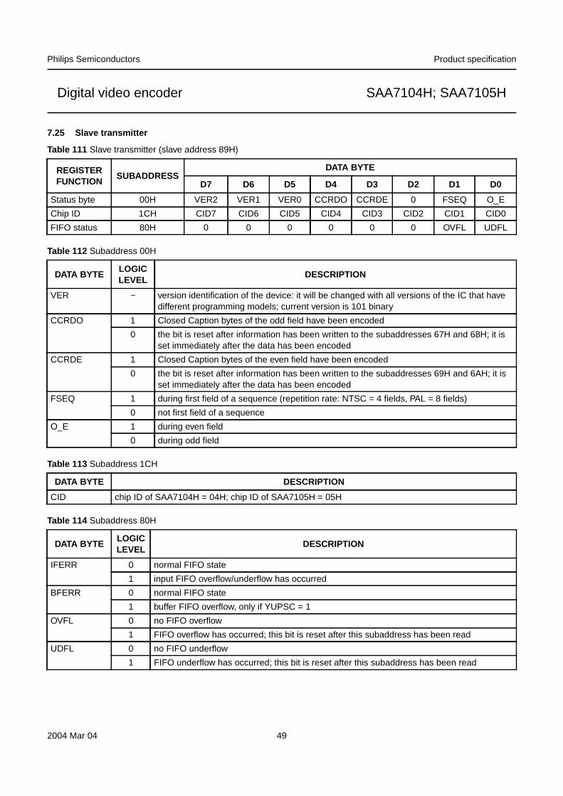
Philips Semiconductors Product specification
Digital video encoder SAA7104H; SAA7105H
7.25 Slave transmitter
Table 111 Slave transmitter (slave address 89H)
Table 112 Subaddress 00H
Table 113 Subaddress 1CH
Table 114 Subaddress 80H
REGISTERFUNCTION
SUBADDRESSDATA BYTE
D7 D6 D5 D4 D3 D2 D1 D0
Status byte 00H VER2 VER1 VER0 CCRDO CCRDE 0 FSEQ O_E
Chip ID 1CH CID7 CID6 CID5 CID4 CID3 CID2 CID1 CID0
FIFO status 80H 0 0 0 0 0 0 OVFL UDFL
DATA BYTELOGICLEVEL
DESCRIPTION
VER − version identification of the device: it will be changed with all versions of the IC that havedifferent programming models; current version is 101 binary
CCRDO 1 Closed Caption bytes of the odd field have been encoded
0 the bit is reset after information has been written to the subaddresses 67H and 68H; it isset immediately after the data has been encoded
CCRDE 1 Closed Caption bytes of the even field have been encoded
0 the bit is reset after information has been written to the subaddresses 69H and 6AH; it isset immediately after the data has been encoded
FSEQ 1 during first field of a sequence (repetition rate: NTSC = 4 fields, PAL = 8 fields)
0 not first field of a sequence
O_E 1 during even field
0 during odd field
DATA BYTE DESCRIPTION
CID chip ID of SAA7104H = 04H; chip ID of SAA7105H = 05H
DATA BYTELOGICLEVEL
DESCRIPTION
IFERR 0 normal FIFO state
1 input FIFO overflow/underflow has occurred
BFERR 0 normal FIFO state
1 buffer FIFO overflow, only if YUPSC = 1
OVFL 0 no FIFO overflow
1 FIFO overflow has occurred; this bit is reset after this subaddress has been read
UDFL 0 no FIFO underflow
1 FIFO underflow has occurred; this bit is reset after this subaddress has been read
2004 Mar 04 49
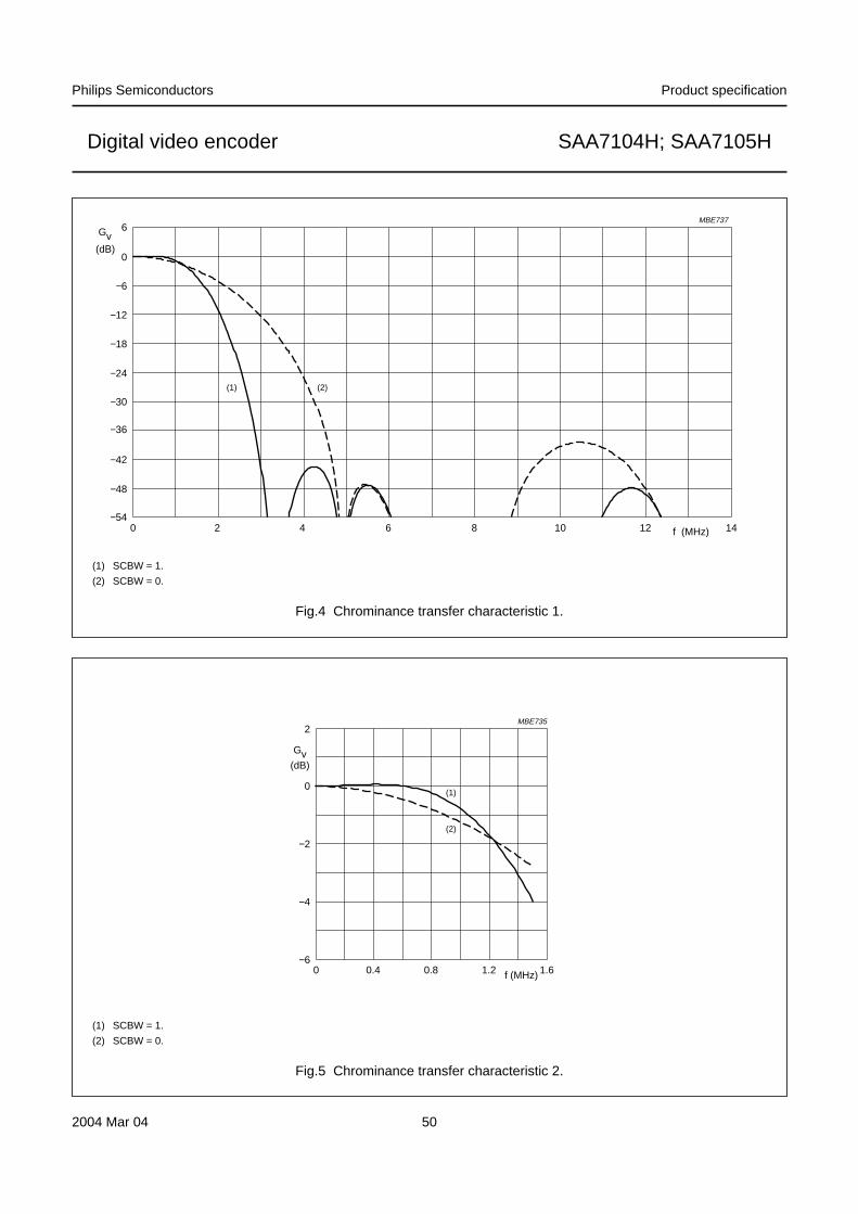
Philips Semiconductors Product specification
Digital video encoder SAA7104H; SAA7105H
handbook, full pagewidth
6 8 10 12 14
6
0
0 2 4
MBE737
−6
−12
−18
−30
−24
−36
−42
−54
−48
f (MHz)
Gv(dB)
(1) (2)
Fig.4 Chrominance transfer characteristic 1.
(1) SCBW = 1.
(2) SCBW = 0.
handbook, halfpage
0 0.4 0.8 1.6
2
0
−4
−6
−2
MBE735
1.2 f (MHz)
Gv(dB)
(1)
(2)
Fig.5 Chrominance transfer characteristic 2.
(1) SCBW = 1.
(2) SCBW = 0.
2004 Mar 04 50
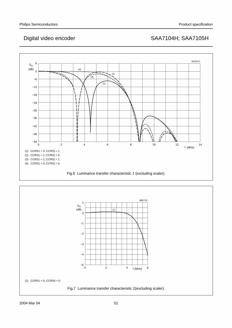
Philips Semiconductors Product specification
Digital video encoder SAA7104H; SAA7105H
handbook, full pagewidth
6
(1)
(2)
(4)
(3)
8 10 12 14
6
0
0 2 4
MGD672
−6
−12
−18
−30
−24
−36
−42
−54
−48
f (MHz)
Gv(dB)
Fig.6 Luminance transfer characteristic 1 (excluding scaler).
(1) CCRS1 = 0; CCRS) = 1.
(2) CCRS1 = 1; CCRS) = 0.
(3) CCRS1 = 1; CCRS) = 1.
(4) CCRS1 = 0; CCRS) = 0.
handbook, halfpage
0 2
(1)
6
1
0
−1
−2
−3
−4
−5
MBE736
4 f (MHz)
Gv(dB)
Fig.7 Luminance transfer characteristic 2(excluding scaler).
(1) CCRS1 = 0; CCRS0 = 0.
2004 Mar 04 51
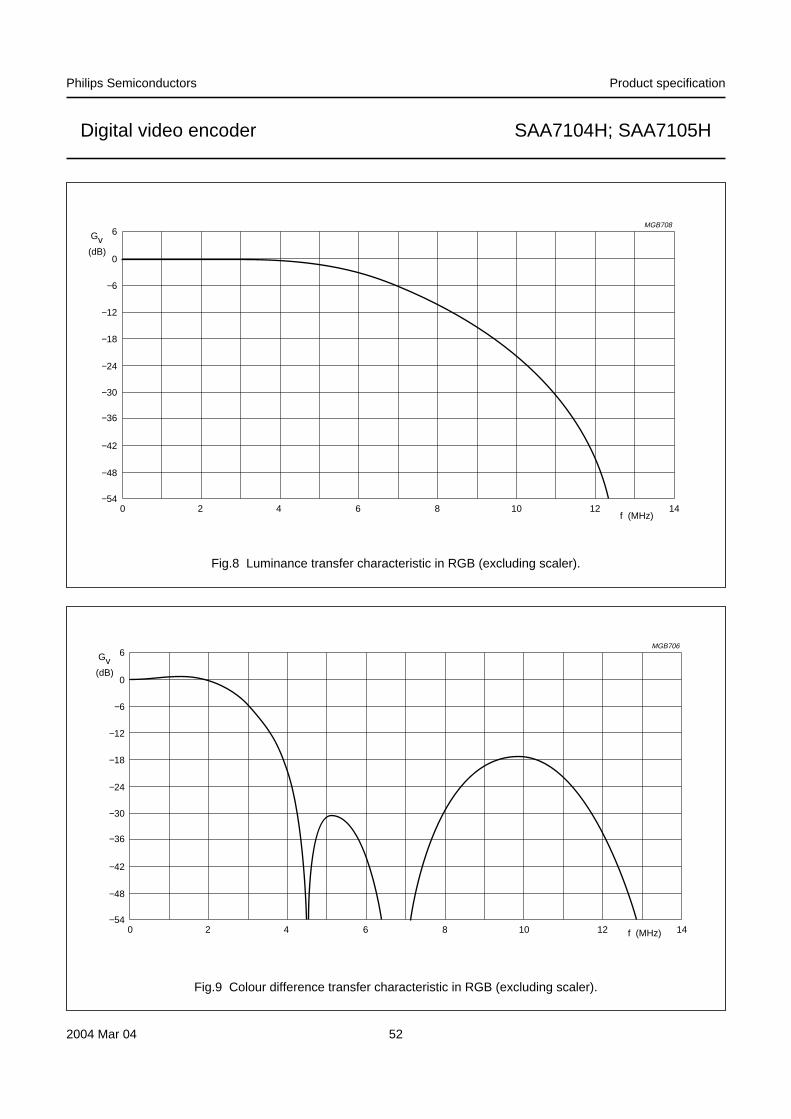
Philips Semiconductors Product specification
Digital video encoder SAA7104H; SAA7105H
handbook, full pagewidth
6 8 10 12 14
6
0
0 2 4
MGB708
−6
−12
−18
−30
−24
−36
−42
−54
−48
f (MHz)
Gv(dB)
Fig.8 Luminance transfer characteristic in RGB (excluding scaler).
handbook, full pagewidth
6 8 10 12 14
6
0
0 2 4
MGB706
−6
−12
−18
−30
−24
−36
−42
−54
−48
f (MHz)
Gv(dB)
Fig.9 Colour difference transfer characteristic in RGB (excluding scaler).
2004 Mar 04 52
Philips Semiconductors Product specification
Digital video encoder SAA7104H; SAA7105H
8 BOUNDARY SCAN TEST
The SAA7104H; SAA7105H has built-in logic and5 dedicated pins to support boundary scan testing whichallows board testing without special hardware (nails). TheSAA7104H; SAA7105H follows the “IEEE Std. 1149.1 -Standard Test Access Port and Boundary-ScanArchitecture” set by the Joint Test Action Group (JTAG)chaired by Philips.
The 5 special pins are Test Mode Select (TMS), TestClock (TCK), Test Reset (TRST), Test Data Input (TDI)and Test Data Output (TDO).
The Boundary Scan Test (BST) functions BYPASS,EXTEST, INTEST, SAMPLE, CLAMP and IDCODE are allsupported; see Table 115. Details about theJTAG BST-TEST can be found in the specification “IEEEStd. 1149.1”. A file containing the detailed Boundary ScanDescription Language (BSDL) of the SAA7104H;SAA7105H is available on request.
Table 115 BST instructions supported by the SAA7104H; SAA7105H
INSTRUCTION DESCRIPTION
BYPASS This mandatory instruction provides a minimum length serial path (1 bit) between TDI and TDOwhen no test operation of the component is required.
EXTEST This mandatory instruction allows testing of off-chip circuitry and board level interconnections.
SAMPLE This mandatory instruction can be used to take a sample of the inputs during normal operation ofthe component. It can also be used to preload data values into the latched outputs of theboundary scan register.
CLAMP This optional instruction is useful for testing when not all ICs have BST. This instruction addressesthe bypass register while the boundary scan register is in external test mode.
IDCODE This optional instruction will provide information on the components manufacturer, part number andversion number.
INTEST This optional instruction allows testing of the internal logic (no support for customer available).
USER1 This private instruction allows testing by the manufacturer (no support for customer available).
8.1 Initialization of boundary scan circuit
The Test Access Port (TAP) controller of an IC should bein the reset state (TEST_LOGIC_RESET) when the IC isin functional mode. This reset state also forces theinstruction register into a functional instruction such asIDCODE or BYPASS.
To solve the power-up reset, the standard specifies thatthe TAP controller will be forced asynchronously to theTEST_LOGIC_RESET state by setting the TRST pinLOW.
8.2 Device identification codes
A device identification register is specified in “IEEE Std.1149.1b-1994”. It is a 32-bit register which contains fieldsfor the specification of the IC manufacturer, the IC partnumber and the IC version number. Its biggest advantageis the possibility to check for the correct ICs mounted afterproduction and to determine the version number of the ICsduring field service.
When the IDCODE instruction is loaded into the BSTinstruction register, the identification register will beconnected between TDI and TDO of the IC.The identification register will load a component specificcode during the CAPTURE_DATA_REGISTER state ofthe TAP controller, this code can subsequently be shiftedout. At board level this code can be used to verifycomponent manufacturer, type and version number. Thedevice identification register contains 32 bits, numbered31 to 0, where bit 31 is the most significant bit (nearest toTDI) and bit 0 is the least significant bit (nearest to TDO);see Fig.10.
2004 Mar 04 53
Philips Semiconductors Product specification
Digital video encoder SAA7104H; SAA7105H
handbook, full pagewidth
0000001010101110001000001000101
4-bitversioncode
16-bit part number 11-bit manufactureridentification
TDI TDO
31
MSB LSB
28 27 12 11 1 0
1
MHC568
handbook, full pagewidth
0000001010101110001000001010101
4-bitversioncode
16-bit part number 11-bit manufactureridentification
TDI TDO
31
MSB LSB
28 27 12 11 1 0
1
MHC569
Fig.10 32 bits of identification code.
b. SAA7105H.
a. SAA7104H.
9 LIMITING VALUESIn accordance with the Absolute Maximum Rating System (IEC 60134); all ground pins connected together andgrounded (0 V); all supply pins connected together.
Notes
1. Condition for maximum voltage at digital inputs or I/O pins: 3.0 V < VDDD < 3.6 V.
2. Class 2 according to EIA/JESD22-114-B.
3. Class B according to EIA/JESD22-115-A.
SYMBOL PARAMETER CONDITIONS MIN. MAX. UNIT
VDDD digital supply voltage −0.5 +4.6 V
VDDA analog supply voltage −0.5 +4.6 V
Vi(A) input voltage at analog inputs −0.5 +4.6 V
Vi(n) input voltage at pins XTALI, SDA and SCL −0.5 VDDD + 0.5 V
Vi(D) input voltage at digital inputs or I/O pins outputs in 3-state −0.5 +4.6 V
outputs in 3-state;note 1
−0.5 +5.5 V
∆VSS voltage difference between VSSA(n) and VSSD(n) − 100 mV
Tstg storage temperature −65 +150 °CTamb ambient temperature 0 70 °CVesd electrostatic discharge voltage human body model;
note 2− ±2000 V
machine model;note 3
− ±200 V
2004 Mar 04
54
Philips Semiconductors Product specification
Digital video encoder SAA7104H; SAA7105H
10 THERMAL CHARACTERISTICS
Note
1. The overall Rth(j-a) value can vary depending on the board layout. To minimize the effective Rth(j-a) all power andground pins must be connected to the power and ground layers directly. An ample copper area direct under theSAA7104H; SAA7105H with a number of through-hole plating, which connect to the ground layer (four-layer board:second layer), can also reduce the effective Rth(j-a). Please do not use any solder-stop varnish under the chip. Inaddition the usage of soldering glue with a high thermal conductance after curing is recommended.
11 CHARACTERISTICSTamb = 0 to 70 °C (typical values excluded); unless otherwise specified.
SYMBOL PARAMETER CONDITIONS VALUE UNIT
Rth(j-a) thermal resistance from junction to ambient in free air 44(1) K/W
SYMBOL PARAMETER CONDITIONS MIN. TYP. MAX. UNIT
Supplies
VDDA analog supply voltage 3.15 3.3 3.45 V
VDDD2,VDDD3,VDDD4
digital supply voltage 3.15 3.3 3.45 V
VDDD1 digital supply voltage (DVO) 1.045 1.1 1.155 V
1.425 1.5 1.575 V
1.71 1.8 1.89 V
2.375 2.5 2.625 V
3.135 3.3 3.465 V
IDDA analog supply current note 1 1 110 115 mA
IDDD digital supply current note 2 1 175 200 mA
Inputs
VIL LOW-level input voltage VDDD1 = 1.1 V, 1.5 V, 1.8 Vor 2.5 V; note 3
−0.1 − +0.2 V
VDDD1 = 3.3 V; note 3 −0.5 − +0.8 V
pins RESET, TMS, TCK,TRST and TDI
−0.5 − +0.8 V
VIH HIGH-level input voltage VDDD1 = 1.1 V, 1.5 V, 1.8 Vor 2.5 V; note 3
VDDD1 − 0.2 − VDDD1 + 0.1 V
VDDD1 = 3.3 V; note 3 2 − VDDD1 + 0.3 V
pins RESET, TMS, TCK,TRST and TDI
2 − VDDD2 + 0.3 V
ILI input leakage current − − 10 µA
Ci input capacitance clocks − − 10 pF
data − − 10 pF
I/Os at high-impedance − − 10 pF
2004 Mar 04 55
Philips Semiconductors Product specification
Digital video encoder SAA7104H; SAA7105H
Outputs
VOL LOW-level output voltage VDDD1 = 1.1 V, 1.5 V, 1.8 Vor 2.5 V; note 3
0 − 0.1 V
VDDD1 = 3.3 V; note 3 0 − 0.4 V
pins TDO,TTXRQ_XCLKO2, VSMand HSM_CSYNC
0 − 0.4 V
VOH HIGH-level output voltage VDDD1 = 1.1 V, 1.5 V, 1.8 Vor 2.5 V; note 3
VDDD1 − 0.1 − VDDD1 V
VDDD1 = 3.3 V; note 3 2.4 − VDDD1 V
pins TDO,TTXRQ_XCLKO2, VSMand HSM_CSYNC
2.4 − VDDD2 V
I2C-bus; pins SDA and SCL
VIL LOW-level input voltage −0.5 − 0.3VDDD2 V
VIH HIGH-level input voltage 0.7VDDD2 − VDDD2 + 0.3 V
Ii input current Vi = LOW or HIGH −10 − +10 µA
VOL LOW-level output voltage(pin SDA)
IOL = 3 mA − − 0.4 V
Io output current during acknowledge 3 − − mA
Clock timing; pins PIXCLKI and PIXCLKO
TPIXCLK cycle time note 4 12 − − ns
td(CLKD) delay from PIXCLKO toPIXCLKI
note 5 − − − ns
δ duty factor tHIGH/TPIXCLK note 4 40 50 60 %
duty factor tHIGH/TCLKO2 output 40 50 60 %
tr rise time note 4 − − 1.5 ns
tf fall time note 4 − − 1.5 ns
Input timing
tSU;DAT input data set-up time pins PD11 to PD0, RTCIand TTX_SRES
2 − − ns
tHD;DAT input data hold time pins PD11 to PD0, RTCIand TTX_SRES
1.5 − − ns
tSU;DAT input data set-up time pins HSVGC, VSVGCand FSVGC; note 6
2 − − ns
tHD;DAT input data hold time pins HSVGC, VSVGCand FSVGC; note 6
1.5 − − ns
Crystal oscillator
fnom nominal frequency − 27 − MHz
∆f/fnom permissible deviation ofnominal frequency
note 7 −50 − +50 10−6
SYMBOL PARAMETER CONDITIONS MIN. TYP. MAX. UNIT
2004 Mar 04 56
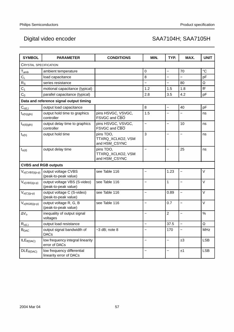
Philips Semiconductors Product specification
Digital video encoder SAA7104H; SAA7105H
CRYSTAL SPECIFICATION
Tamb ambient temperature 0 − 70 °CCL load capacitance 8 − − pF
RS series resistance − − 80 ΩC1 motional capacitance (typical) 1.2 1.5 1.8 fF
C0 parallel capacitance (typical) 2.8 3.5 4.2 pF
Data and reference signal output timing
Co(L) output load capacitance 8 − 40 pF
to(h)(gfx) output hold time to graphicscontroller
pins HSVGC, VSVGC,FSVGC and CBO
1.5 − − ns
to(d)(gfx) output delay time to graphicscontroller
pins HSVGC, VSVGC,FSVGC and CBO
− − 10 ns
to(h) output hold time pins TDO,TTXRQ_XCLKO2, VSMand HSM_CSYNC
3 − − ns
to(d) output delay time pins TDO,TTXRQ_XCLKO2, VSMand HSM_CSYNC
− − 25 ns
CVBS and RGB outputs
Vo(CVBS)(p-p) output voltage CVBS(peak-to-peak value)
see Table 116 − 1.23 − V
Vo(VBS)(p-p) output voltage VBS (S-video)(peak-to-peak value)
see Table 116 − 1 − V
Vo(C)(p-p) output voltage C (S-video)(peak-to-peak value)
see Table 116 − 0.89 − V
Vo(RGB)(p-p) output voltage R, G, B(peak-to-peak value)
see Table 116 − 0.7 − V
∆Vo inequality of output signalvoltages
− 2 − %
Ro(L) output load resistance − 37.5 − ΩBDAC output signal bandwidth of
DACs−3 dB; note 8 − 170 − MHz
ILElf(DAC) low frequency integral linearityerror of DACs
− − ±3 LSB
DLElf(DAC) low frequency differentiallinearity error of DACs
− − ±1 LSB
SYMBOL PARAMETER CONDITIONS MIN. TYP. MAX. UNIT
2004 Mar 04 57
Philips Semiconductors Product specification
Digital video encoder SAA7104H; SAA7105H
Notes
1. Minimum value for I2C-bus bit DOWNA = 1.
2. Minimum value for I2C-bus bit DOWND = 1.
3. Levels refer to pins PD11 to PD0, PIXCLKI, FSVGC, PIXCLKI, VSVGC, PIXCLKO, CBO, TVD, and HSVGC, beinginputs or outputs directly connected to a graphics controller.Input sensitivity is 1/2VDDD2 + 100 mV for HIGH and 1/2VDDD2 − 100 mV for LOW.The reference voltage 1/2VDDD2 is generated on chip.
4. The data is for both input and output direction.
5. This parameter is arbitrary, if PIXCLKI is looped through the VGC.
6. Tested with programming IFBP = 1.
7. If an internal oscillator is used, crystal deviation of nominal frequency is directly proportional to the deviation ofsubcarrier frequency and line/field frequency.
8. with RL = 37.5 Ω and Cext = 20 pF (typical).B 3 dB–1
2πRL Cext 5 pF+( )------------------------------------------------=
2004 Mar 04 58
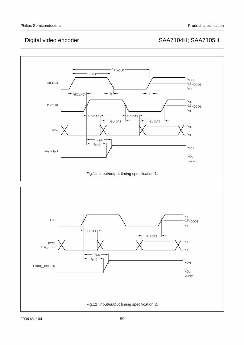
Philips Semiconductors Product specification
Digital video encoder SAA7104H; SAA7105H
handbook, full pagewidth
PIXCLKO
PIXCLKI
PDn
any output
td(CLKD)
tHIGH
tf tr
VOH0.5VDDD1VOL
tHD;DATtHD;DAT
to(h)
to(d)
tSU;DATtSU;DAT
TPIXCLK
VIH0.5VDDD1VIL
VOH
VOL
VIH
VIL
MHC567
Fig.11 Input/output timing specification 1.
handbook, full pagewidth
LLC
RTCI,TTX_SRES
TTXRQ_XCLKO2
tHD;DAT
to(h)
to(d)
tSU;DAT
VIH0.5VDDD1VIL
VOH
VOL
MHC685
VIH
VIL
Fig.12 Input/output timing specification 2.
2004 Mar 04 59
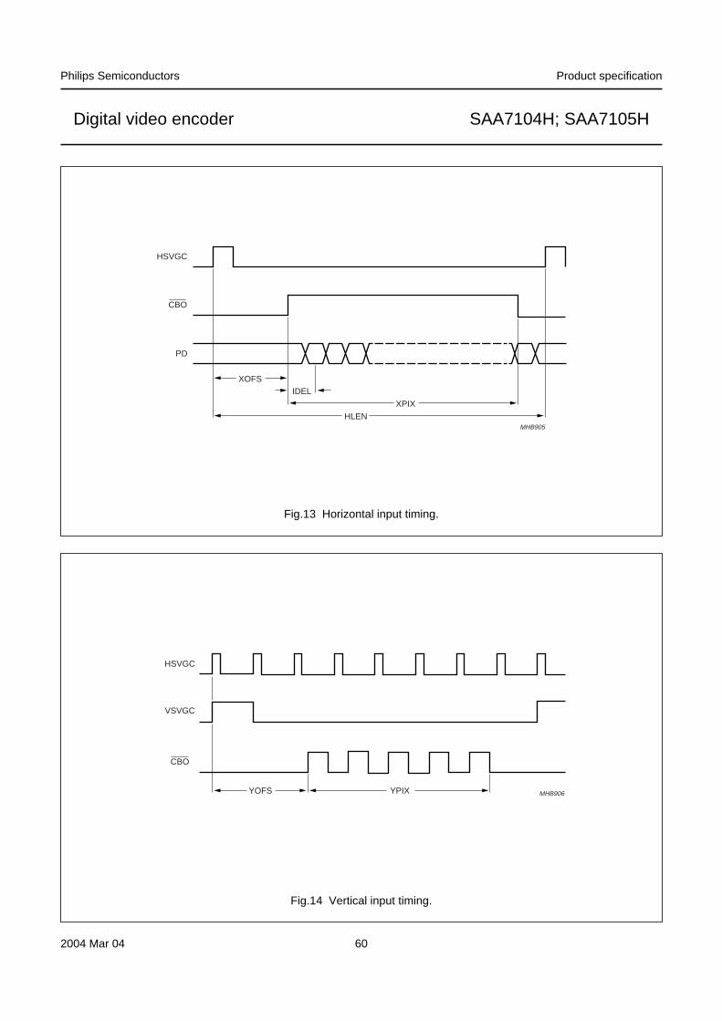
Philips Semiconductors Product specification
Digital video encoder SAA7104H; SAA7105H
handbook, full pagewidthHSVGC
PD
CBO
XOFSIDEL
XPIX
HLENMHB905
Fig.13 Horizontal input timing.
handbook, full pagewidthHSVGC
VSVGC
CBO
YOFS YPIX MHB906
Fig.14 Vertical input timing.
2004 Mar 04 60
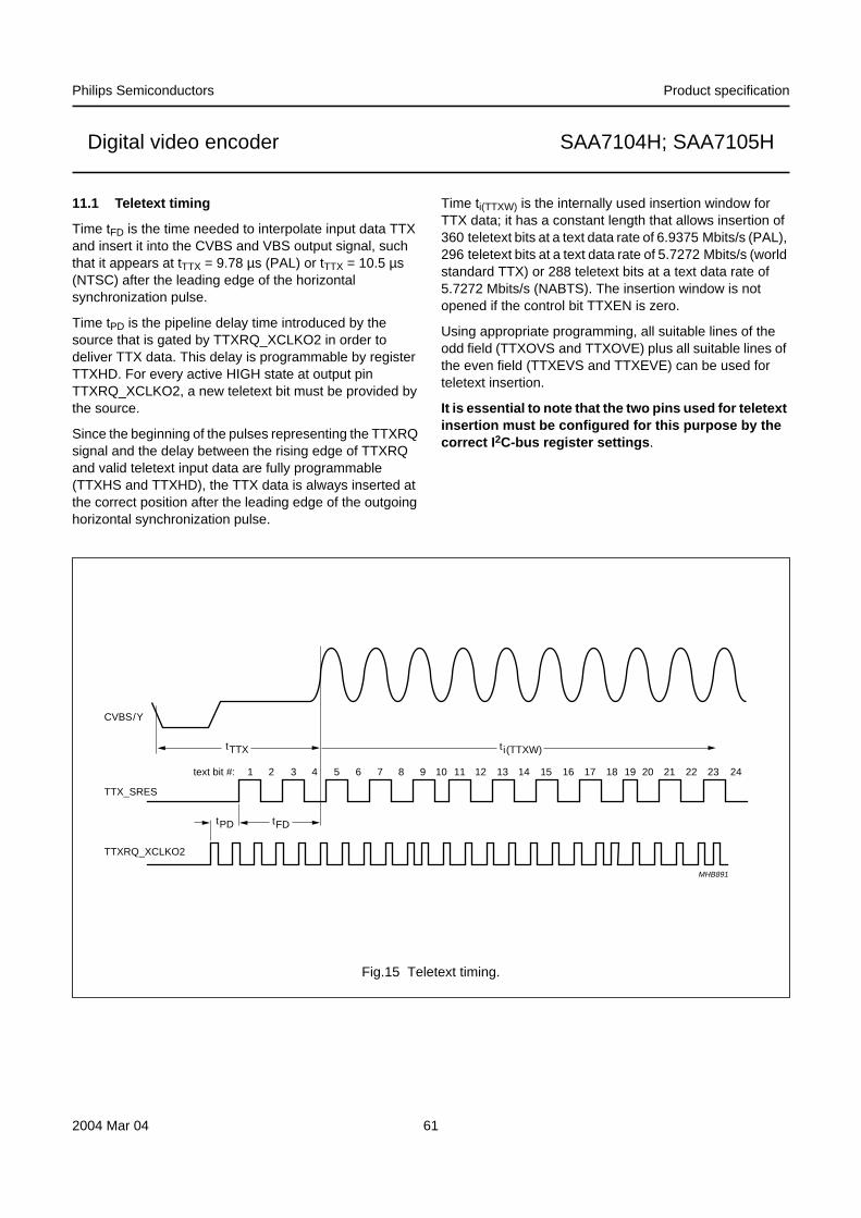
Philips Semiconductors Product specification
Digital video encoder SAA7104H; SAA7105H
11.1 Teletext timing
Time tFD is the time needed to interpolate input data TTXand insert it into the CVBS and VBS output signal, suchthat it appears at tTTX = 9.78 µs (PAL) or tTTX = 10.5 µs(NTSC) after the leading edge of the horizontalsynchronization pulse.
Time tPD is the pipeline delay time introduced by thesource that is gated by TTXRQ_XCLKO2 in order todeliver TTX data. This delay is programmable by registerTTXHD. For every active HIGH state at output pinTTXRQ_XCLKO2, a new teletext bit must be provided bythe source.
Since the beginning of the pulses representing the TTXRQsignal and the delay between the rising edge of TTXRQand valid teletext input data are fully programmable(TTXHS and TTXHD), the TTX data is always inserted atthe correct position after the leading edge of the outgoinghorizontal synchronization pulse.
Time ti(TTXW) is the internally used insertion window forTTX data; it has a constant length that allows insertion of360 teletext bits at a text data rate of 6.9375 Mbits/s (PAL),296 teletext bits at a text data rate of 5.7272 Mbits/s (worldstandard TTX) or 288 teletext bits at a text data rate of5.7272 Mbits/s (NABTS). The insertion window is notopened if the control bit TTXEN is zero.
Using appropriate programming, all suitable lines of theodd field (TTXOVS and TTXOVE) plus all suitable lines ofthe even field (TTXEVS and TTXEVE) can be used forteletext insertion.
It is essential to note that the two pins used for teletextinsertion must be configured for this purpose by thecorrect I 2C-bus register settings .
handbook, full pagewidth
ti(TTXW)tTTX
tPD tFD
CVBS/Y
TTX_SRES
TTXRQ_XCLKO2
text bit #: 1 2 3 4 5 6 7 8 9 10 11 12 13 14 15 16 17 18 19 20 21 22 23 24
MHB891
Fig.15 Teletext timing.
2004 Mar 04 61
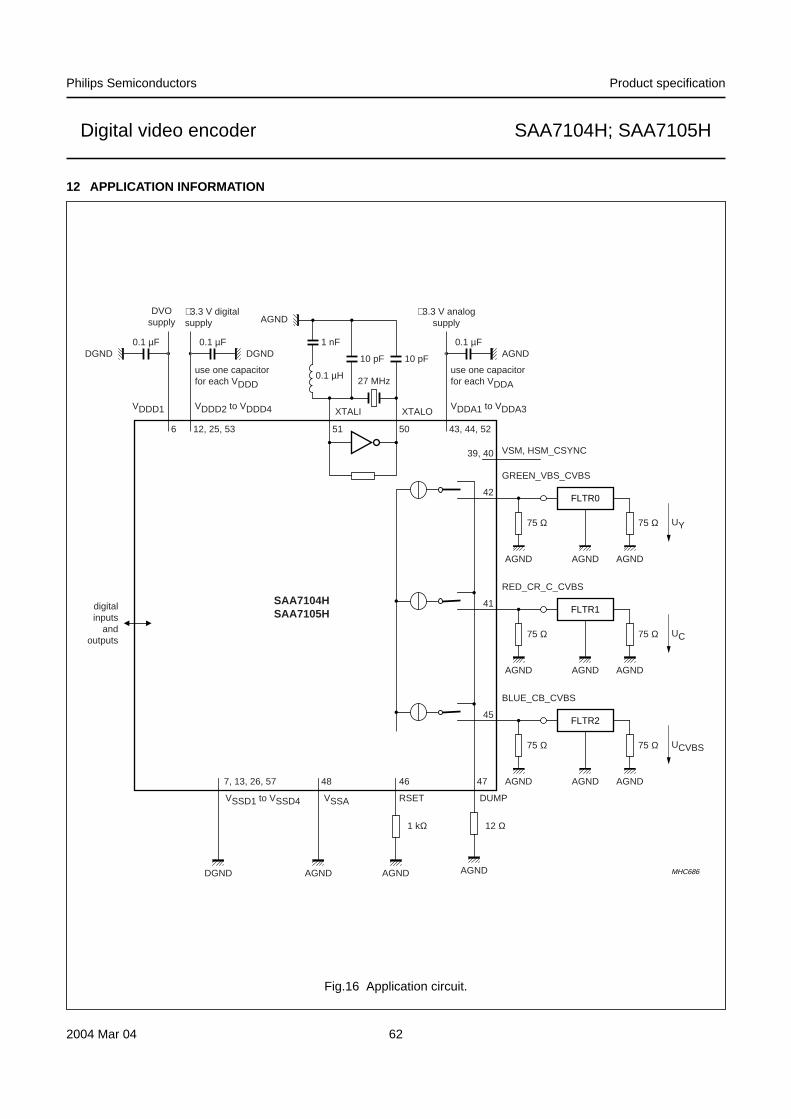
Philips Semiconductors Product specification
Digital video encoder SAA7104H; SAA7105H
12 APPLICATION INFORMATION
handbook, full pagewidth
MHC686
FLTR0
DGND
AGNDDVO
supply+3.3 V digitalsupply
+3.3 V analogsupply
DGND 10 pF
27 MHz0.1 µH
0.1 µF 0.1 µF 0.1 µF1 nF
10 pF AGND
VDDD2 to VDDD4
VSSD1 to VSSD4 VSSA RSET DUMP
VDDA1 to VDDA3
GREEN_VBS_CVBS
use one capacitorfor each VDDD
use one capacitorfor each VDDA
VDDD1
digitalinputs
andoutputs
XTALI XTALO
AGND
AGNDAGNDDGND AGND
75 Ω
6 51 50 43, 44, 52
39, 40
42
41
45
4746487, 13, 26, 57
12, 25, 53
75 Ω
AGND AGND
UY
FLTR1
RED_CR_C_CVBS
AGND
75 Ω
1 kΩ 12 Ω
75 Ω
AGND AGND
UC
FLTR2
BLUE_CB_CVBS
VSM, HSM_CSYNC
AGND
75 Ω 75 Ω
AGND AGND
UCVBS
SAA7104HSAA7105H
Fig.16 Application circuit.
2004 Mar 04 62
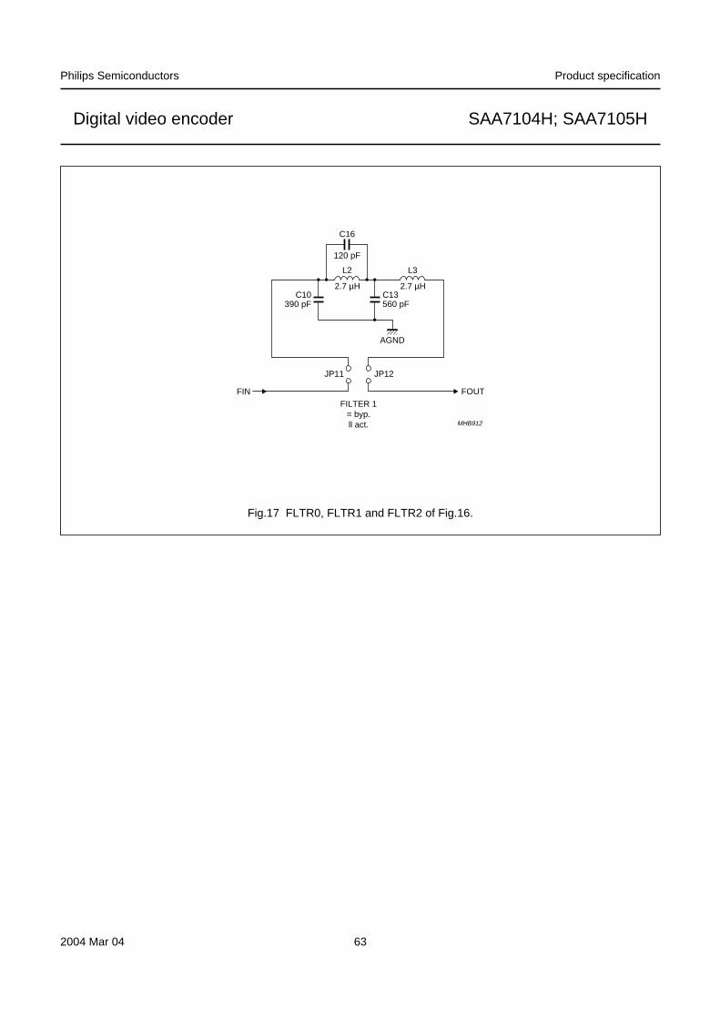
Philips Semiconductors Product specification
Digital video encoder SAA7104H; SAA7105H
handbook, halfpage
MHB912
2.7 µH
120 pF
C16
JP11 JP12
FIN FOUT
C10390 pF
C13560 pF
L2
2.7 µH
L3
FILTER 1= byp.ll act.
AGND
Fig.17 FLTR0, FLTR1 and FLTR2 of Fig.16.
2004 Mar 04 63
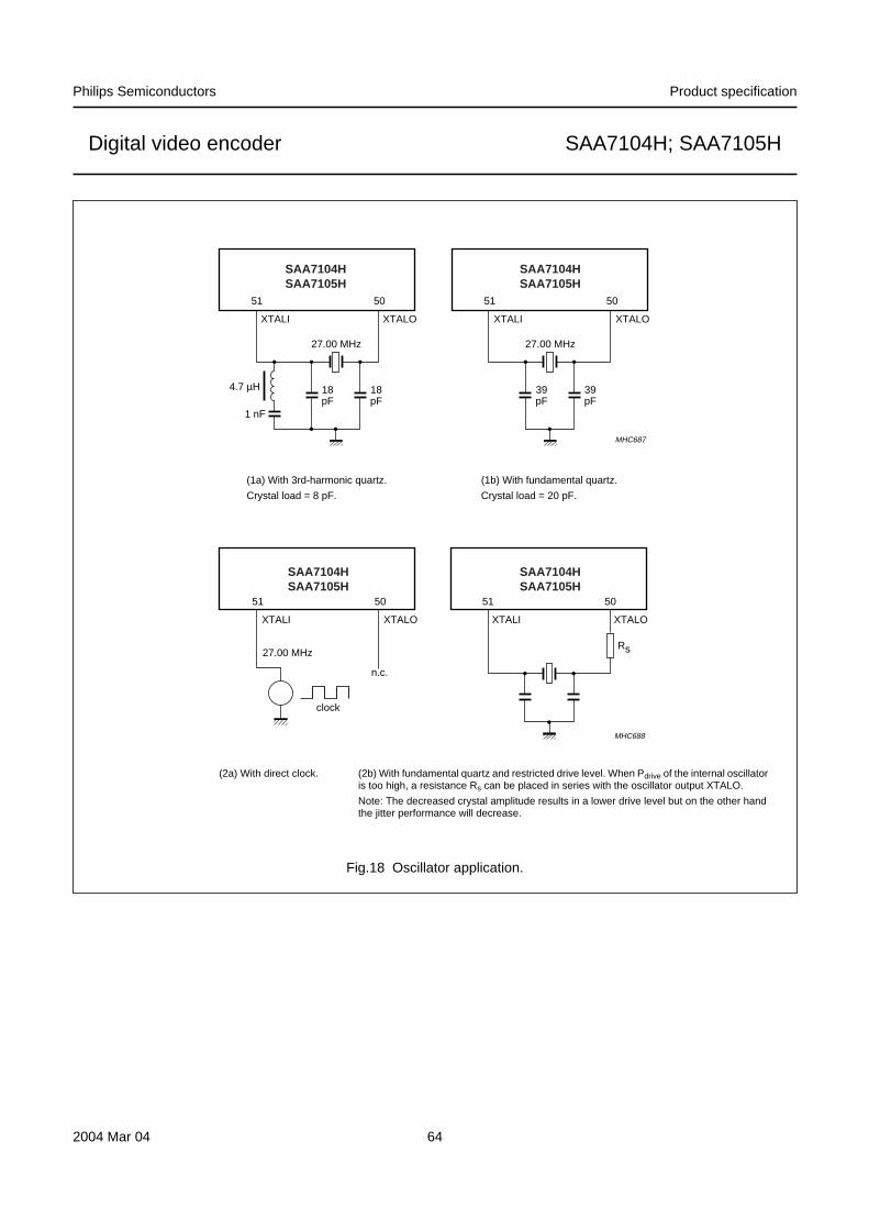
Philips Semiconductors Product specification
Digital video encoder SAA7104H; SAA7105H
handbook, full pagewidth
39pF
39pF
27.00 MHz
18pF
1 nF
4.7 µH 18pF
27.00 MHz
SAA7104HSAA7105H
SAA7104HSAA7105H
51
XTALI XTALO
50 51
XTALI XTALO
50
MHC687
handbook, full pagewidth
Rs
n.c.
clock
27.00 MHz
SAA7104HSAA7105H
SAA7104HSAA7105H
51
XTALI XTALO
50 51
XTALI XTALO
50
MHC688
Fig.18 Oscillator application.
(1a) With 3rd-harmonic quartz.
Crystal load = 8 pF.
(1b) With fundamental quartz.
Crystal load = 20 pF.
(2a) With direct clock. (2b) With fundamental quartz and restricted drive level. When Pdrive of the internal oscillatoris too high, a resistance Rs can be placed in series with the oscillator output XTALO.
Note: The decreased crystal amplitude results in a lower drive level but on the other handthe jitter performance will decrease.
2004 Mar 04 64
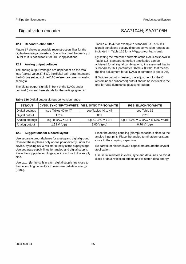
Philips Semiconductors Product specification
Digital video encoder SAA7104H; SAA7105H
12.1 Reconstruction filter
Figure 17 shows a possible reconstruction filter for thedigital-to-analog converters. Due to its cut-off frequency of∼6 MHz, it is not suitable for HDTV applications.
12.2 Analog output voltages
The analog output voltages are dependent on the totalload (typical value 37.5 Ω), the digital gain parameters andthe I2C-bus settings of the DAC reference currents (analogsettings).
The digital output signals in front of the DACs undernominal (nominal here stands for the settings given in
Tables 40 to 47 for example a standard PAL or NTSCsignal) conditions occupy different conversion ranges, asindicated in Table 116 for a 100⁄100 colour bar signal.
By setting the reference currents of the DACs as shown inTable 116, standard compliant amplitudes can beachieved for all signal combinations; it is assumed that insubaddress 16H, parameter DACF = 0000b, that meansthe fine adjustment for all DACs in common is set to 0%.
If S-video output is desired, the adjustment for the C(chrominance subcarrier) output should be identical to theone for VBS (luminance plus sync) output.
Table 116 Digital output signals conversion range
SET/OUT CVBS, SYNC TIP-TO-WHITE VBS, SYNC TIP-TO-WHITE RGB, BLACK-TO-WHITE
Digital settings see Tables 40 to 47 see Tables 40 to 47 see Table 35
Digital output 1014 881 876
Analog settings e.g. B DAC = 1FH e.g. G DAC = 1BH e.g. R DAC = G DAC = B DAC = 0BH
Analog output 1.23 V (p-p) 1.00 V (p-p) 0.70 V (p-p)
12.3 Suggestions for a board layout
Use separate ground planes for analog and digital ground.Connect these planes only at one point directly under thedevice, by using a 0 Ω resistor directly at the supply stage.Use separate supply lines for analog and digital supply.Place the supply decoupling capacitors close to the supplypins.
Use Lbead (ferrite coil) in each digital supply line close tothe decoupling capacitors to minimize radiation energy(EMC).
Place the analog coupling (clamp) capacitors close to theanalog input pins. Place the analog termination resistorsclose to the coupling capacitors.
Be careful of hidden layout capacitors around the crystalapplication.
Use serial resistors in clock, sync and data lines, to avoidclock or data reflection effects and to soften data energy.
2004 Mar 04 65
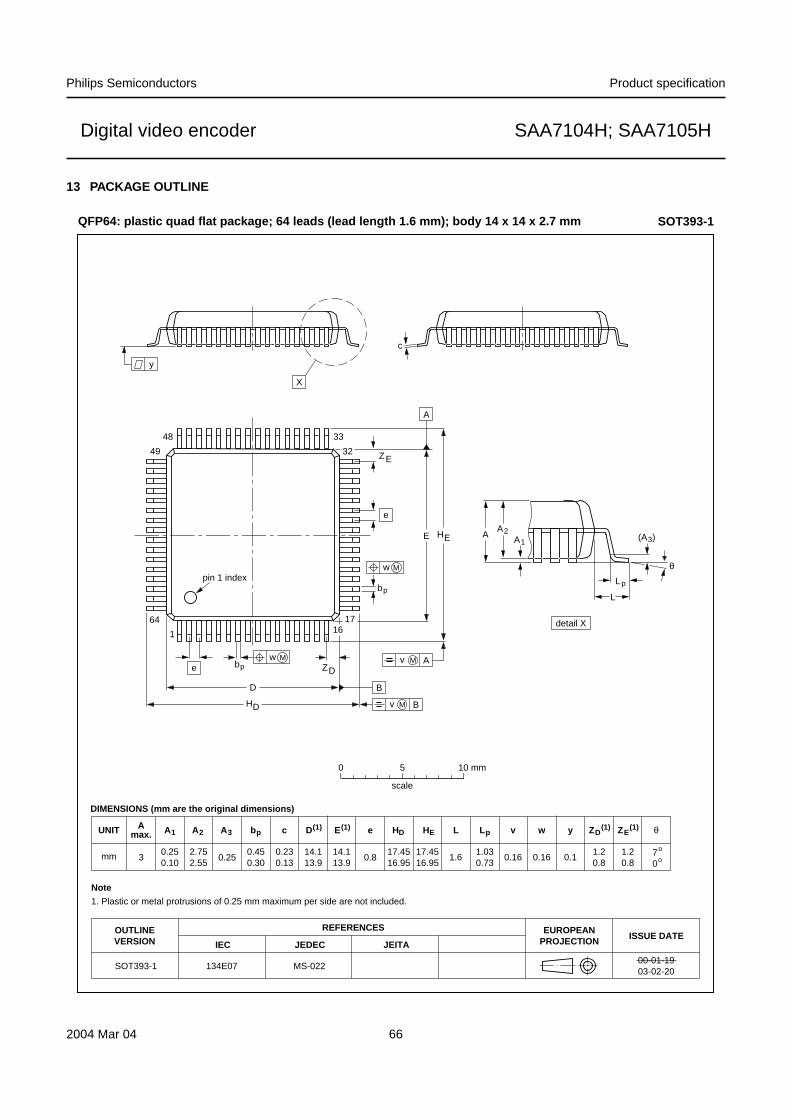
Philips Semiconductors Product specification
Digital video encoder SAA7104H; SAA7105H
13 PACKAGE OUTLINE
UNIT A1 A2 A3 bp c E(1) e HE L L p Zywv θ
REFERENCESOUTLINEVERSION
EUROPEANPROJECTION ISSUE DATE
IEC JEDEC JEITA
mm 0.250.10
2.752.55
0.250.450.30
0.230.13
14.113.9
0.817.4516.95
1.20.8
70
o
o0.16 0.10.161.6
DIMENSIONS (mm are the original dimensions)
Note
1. Plastic or metal protrusions of 0.25 mm maximum per side are not included.
1.030.73
SOT393-1 134E07 MS-02200-01-1903-02-20
D(1) (1)(1)
14.113.9
HD
17.4516.95
EZ
1.20.8
D
e
θ
E A1A
Lp
detail X
L
(A )3
B
16
y
c
EHA2
D
ZD
A
ZE
e
v M A
1
64
49
48 33
32
17
X
bp
DH
bp
v M B
w M
w M
0 5 10 mm
scale
pin 1 index
QFP64: plastic quad flat package; 64 leads (lead length 1.6 mm); body 14 x 14 x 2.7 mm SOT393-1
Amax.
3
2004 Mar 04 66
Philips Semiconductors Product specification
Digital video encoder SAA7104H; SAA7105H
14 SOLDERING
14.1 Introduction to soldering surface mountpackages
This text gives a very brief insight to a complex technology.A more in-depth account of soldering ICs can be found inour “Data Handbook IC26; Integrated Circuit Packages”(document order number 9398 652 90011).
There is no soldering method that is ideal for all surfacemount IC packages. Wave soldering can still be used forcertain surface mount ICs, but it is not suitable for fine pitchSMDs. In these situations reflow soldering isrecommended.
14.2 Reflow soldering
Reflow soldering requires solder paste (a suspension offine solder particles, flux and binding agent) to be appliedto the printed-circuit board by screen printing, stencilling orpressure-syringe dispensing before package placement.Driven by legislation and environmental forces theworldwide use of lead-free solder pastes is increasing.
Several methods exist for reflowing; for example,convection or convection/infrared heating in a conveyortype oven. Throughput times (preheating, soldering andcooling) vary between 100 and 200 seconds dependingon heating method.
Typical reflow peak temperatures range from215 to 270 °C depending on solder paste material. Thetop-surface temperature of the packages shouldpreferably be kept:
• below 225 °C (SnPb process) or below 245 °C (Pb-freeprocess)
– for all BGA, HTSSON-T and SSOP-T packages
– for packages with a thickness ≥ 2.5 mm
– for packages with a thickness < 2.5 mm and avolume ≥ 350 mm3 so called thick/large packages.
• below 240 °C (SnPb process) or below 260 °C (Pb-freeprocess) for packages with a thickness < 2.5 mm and avolume < 350 mm3 so called small/thin packages.
Moisture sensitivity precautions, as indicated on packing,must be respected at all times.
14.3 Wave soldering
Conventional single wave soldering is not recommendedfor surface mount devices (SMDs) or printed-circuit boardswith a high component density, as solder bridging andnon-wetting can present major problems.
To overcome these problems the double-wave solderingmethod was specifically developed.
If wave soldering is used the following conditions must beobserved for optimal results:
• Use a double-wave soldering method comprising aturbulent wave with high upward pressure followed by asmooth laminar wave.
• For packages with leads on two sides and a pitch (e):
– larger than or equal to 1.27 mm, the footprintlongitudinal axis is preferred to be parallel to thetransport direction of the printed-circuit board;
– smaller than 1.27 mm, the footprint longitudinal axismust be parallel to the transport direction of theprinted-circuit board.
The footprint must incorporate solder thieves at thedownstream end.
• For packages with leads on four sides, the footprint mustbe placed at a 45° angle to the transport direction of theprinted-circuit board. The footprint must incorporatesolder thieves downstream and at the side corners.
During placement and before soldering, the package mustbe fixed with a droplet of adhesive. The adhesive can beapplied by screen printing, pin transfer or syringedispensing. The package can be soldered after theadhesive is cured.
Typical dwell time of the leads in the wave ranges from3 to 4 seconds at 250 °C or 265 °C, depending on soldermaterial applied, SnPb or Pb-free respectively.
A mildly-activated flux will eliminate the need for removalof corrosive residues in most applications.
14.4 Manual soldering
Fix the component by first soldering twodiagonally-opposite end leads. Use a low voltage (24 V orless) soldering iron applied to the flat part of the lead.Contact time must be limited to 10 seconds at up to300 °C.
When using a dedicated tool, all other leads can besoldered in one operation within 2 to 5 seconds between270 and 320 °C.
2004 Mar 04 67
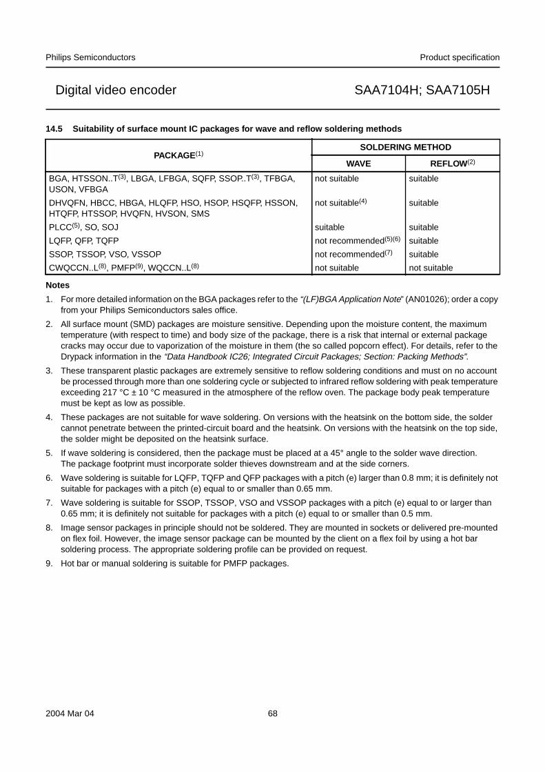
Philips Semiconductors Product specification
Digital video encoder SAA7104H; SAA7105H
14.5 Suitability of surface mount IC packages for wave and reflow soldering methods
Notes
1. For more detailed information on the BGA packages refer to the “(LF)BGA Application Note” (AN01026); order a copyfrom your Philips Semiconductors sales office.
2. All surface mount (SMD) packages are moisture sensitive. Depending upon the moisture content, the maximumtemperature (with respect to time) and body size of the package, there is a risk that internal or external packagecracks may occur due to vaporization of the moisture in them (the so called popcorn effect). For details, refer to theDrypack information in the “Data Handbook IC26; Integrated Circuit Packages; Section: Packing Methods”.
3. These transparent plastic packages are extremely sensitive to reflow soldering conditions and must on no accountbe processed through more than one soldering cycle or subjected to infrared reflow soldering with peak temperatureexceeding 217 °C ± 10 °C measured in the atmosphere of the reflow oven. The package body peak temperaturemust be kept as low as possible.
4. These packages are not suitable for wave soldering. On versions with the heatsink on the bottom side, the soldercannot penetrate between the printed-circuit board and the heatsink. On versions with the heatsink on the top side,the solder might be deposited on the heatsink surface.
5. If wave soldering is considered, then the package must be placed at a 45° angle to the solder wave direction.The package footprint must incorporate solder thieves downstream and at the side corners.
6. Wave soldering is suitable for LQFP, TQFP and QFP packages with a pitch (e) larger than 0.8 mm; it is definitely notsuitable for packages with a pitch (e) equal to or smaller than 0.65 mm.
7. Wave soldering is suitable for SSOP, TSSOP, VSO and VSSOP packages with a pitch (e) equal to or larger than0.65 mm; it is definitely not suitable for packages with a pitch (e) equal to or smaller than 0.5 mm.
8. Image sensor packages in principle should not be soldered. They are mounted in sockets or delivered pre-mountedon flex foil. However, the image sensor package can be mounted by the client on a flex foil by using a hot barsoldering process. The appropriate soldering profile can be provided on request.
9. Hot bar or manual soldering is suitable for PMFP packages.
PACKAGE (1)SOLDERING METHOD
WAVE REFLOW (2)
BGA, HTSSON..T(3), LBGA, LFBGA, SQFP, SSOP..T(3), TFBGA,USON, VFBGA
not suitable suitable
DHVQFN, HBCC, HBGA, HLQFP, HSO, HSOP, HSQFP, HSSON,HTQFP, HTSSOP, HVQFN, HVSON, SMS
not suitable(4) suitable
PLCC(5), SO, SOJ suitable suitable
LQFP, QFP, TQFP not recommended(5)(6) suitable
SSOP, TSSOP, VSO, VSSOP not recommended(7) suitable
CWQCCN..L(8), PMFP(9), WQCCN..L(8) not suitable not suitable
2004 Mar 04 68
Philips Semiconductors Product specification
Digital video encoder SAA7104H; SAA7105H
15 DATA SHEET STATUS
Notes
1. Please consult the most recently issued data sheet before initiating or completing a design.
2. The product status of the device(s) described in this data sheet may have changed since this data sheet waspublished. The latest information is available on the Internet at URL http://www.semiconductors.philips.com.
3. For data sheets describing multiple type numbers, the highest-level product status determines the data sheet status.
LEVELDATA SHEET
STATUS(1)PRODUCT
STATUS(2)(3) DEFINITION
I Objective data Development This data sheet contains data from the objective specification for productdevelopment. Philips Semiconductors reserves the right to change thespecification in any manner without notice.
II Preliminary data Qualification This data sheet contains data from the preliminary specification.Supplementary data will be published at a later date. PhilipsSemiconductors reserves the right to change the specification withoutnotice, in order to improve the design and supply the best possibleproduct.
III Product data Production This data sheet contains data from the product specification. PhilipsSemiconductors reserves the right to make changes at any time in orderto improve the design, manufacturing and supply. Relevant changes willbe communicated via a Customer Product/Process Change Notification(CPCN).
16 DEFINITIONS
Short-form specification The data in a short-formspecification is extracted from a full data sheet with thesame type number and title. For detailed information seethe relevant data sheet or data handbook.
Limiting values definition Limiting values given are inaccordance with the Absolute Maximum Rating System(IEC 60134). Stress above one or more of the limitingvalues may cause permanent damage to the device.These are stress ratings only and operation of the deviceat these or at any other conditions above those given in theCharacteristics sections of the specification is not implied.Exposure to limiting values for extended periods mayaffect device reliability.
Application information Applications that aredescribed herein for any of these products are forillustrative purposes only. Philips Semiconductors makeno representation or warranty that such applications will besuitable for the specified use without further testing ormodification.
17 DISCLAIMERS
Life support applications These products are notdesigned for use in life support appliances, devices, orsystems where malfunction of these products canreasonably be expected to result in personal injury. PhilipsSemiconductors customers using or selling these productsfor use in such applications do so at their own risk andagree to fully indemnify Philips Semiconductors for anydamages resulting from such application.
Right to make changes Philips Semiconductorsreserves the right to make changes in the products -including circuits, standard cells, and/or software -described or contained herein in order to improve designand/or performance. When the product is in full production(status ‘Production’), relevant changes will becommunicated via a Customer Product/Process ChangeNotification (CPCN). Philips Semiconductors assumes noresponsibility or liability for the use of any of theseproducts, conveys no licence or title under any patent,copyright, or mask work right to these products, andmakes no representations or warranties that theseproducts are free from patent, copyright, or mask workright infringement, unless otherwise specified.
2004 Mar 04 69

Philips Semiconductors Product specification
Digital video encoder SAA7104H; SAA7105H
18 PURCHASE OF PHILIPS I2C COMPONENTS
Purchase of Philips I2C components conveys a license under the Philips’ I2C patent to use thecomponents in the I2C system provided the system conforms to the I2C specification defined byPhilips. This specification can be ordered using the code 9398 393 40011.
2004 Mar 04 70

© Koninklijke Philips Electronics N.V. 2004 SCA76All rights are reserved. Reproduction in whole or in part is prohibited without the prior written consent of the copyright owner.
The information presented in this document does not form part of any quotation or contract, is believed to be accurate and reliable and may be changedwithout notice. No liability will be accepted by the publisher for any consequence of its use. Publication thereof does not convey nor imply any license
Philips Semiconductors – a worldwide company
Contact information
For additional information please visit http://www.semiconductors.philips.com . Fax: +31 40 27 24825For sales offices addresses send e-mail to: [email protected] .
under patent- or other industrial or intellectual property rights.
Printed in The Netherlands R21/01/pp71 Date of release: 2004 Mar 04 Document order number: 9397 750 11437