rtd-based high speed and low power integrated … high speed and low power integrated circuits...
TRANSCRIPT
RTD-based High Speed and Low Power Integrated Circuits
RTD-based High Speed and Low Power Integrated Circuits
2009. 04. 27
Kwangseok Seo
Seoul National University
OutlineOutline
Introduction
RTD/HEMT Integration Technology
RTD-based NRZ-mode D-F/F
MOBILE Using only RTDs
Lateral Scaling of RTD Area
Summary
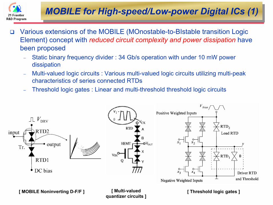
MOBILE for High-speed/Low-power Digital ICs (1)MOBILE for High-speed/Low-power Digital ICs (1)
Various extensions of the MOBILE (MOnostable-to-BIstable transition Logic Element) concept with reduced circuit complexity and power dissipation have been proposed− Static binary frequency divider : 34 Gb/s operation with under 10 mW power
dissipation− Multi-valued logic circuits : Various multi-valued logic circuits utilizing multi-peak
characteristics of series connected RTDs− Threshold logic gates : Linear and multi-threshold threshold logic circuits
[ MOBILE Noninverting D-F/F ] [ Multi-valued quantizer circuits ]
[ Threshold logic gates ]
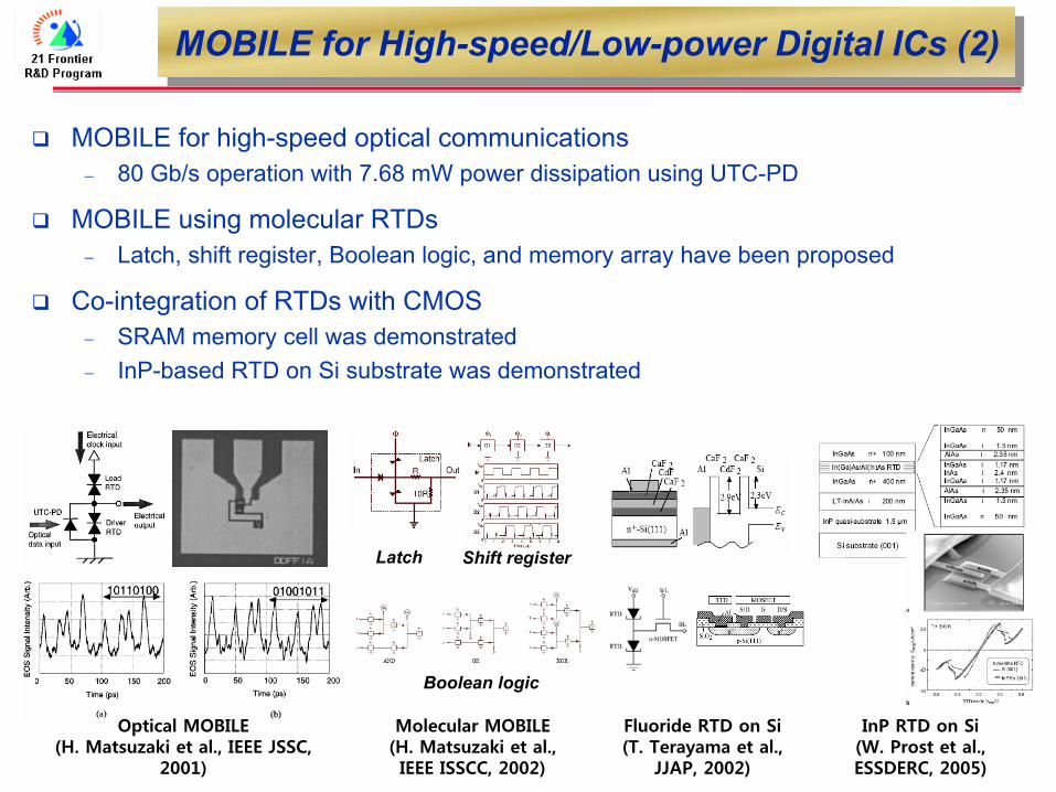
MOBILE for High-speed/Low-power Digital ICs (2)MOBILE for High-speed/Low-power Digital ICs (2)
MOBILE for high-speed optical communications− 80 Gb/s operation with 7.68 mW power dissipation using UTC-PD
MOBILE using molecular RTDs− Latch, shift register, Boolean logic, and memory array have been proposed
Co-integration of RTDs with CMOS− SRAM memory cell was demonstrated− InP-based RTD on Si substrate was demonstrated
Boolean logic
Shift registerLatch
Optical MOBILE(H. Matsuzaki et al., IEEE JSSC,
2001)
Molecular MOBILE(H. Matsuzaki et al., IEEE ISSCC, 2002)
Fluoride RTD on Si(T. Terayama et al.,
JJAP, 2002)
InP RTD on Si(W. Prost et al., ESSDERC, 2005)
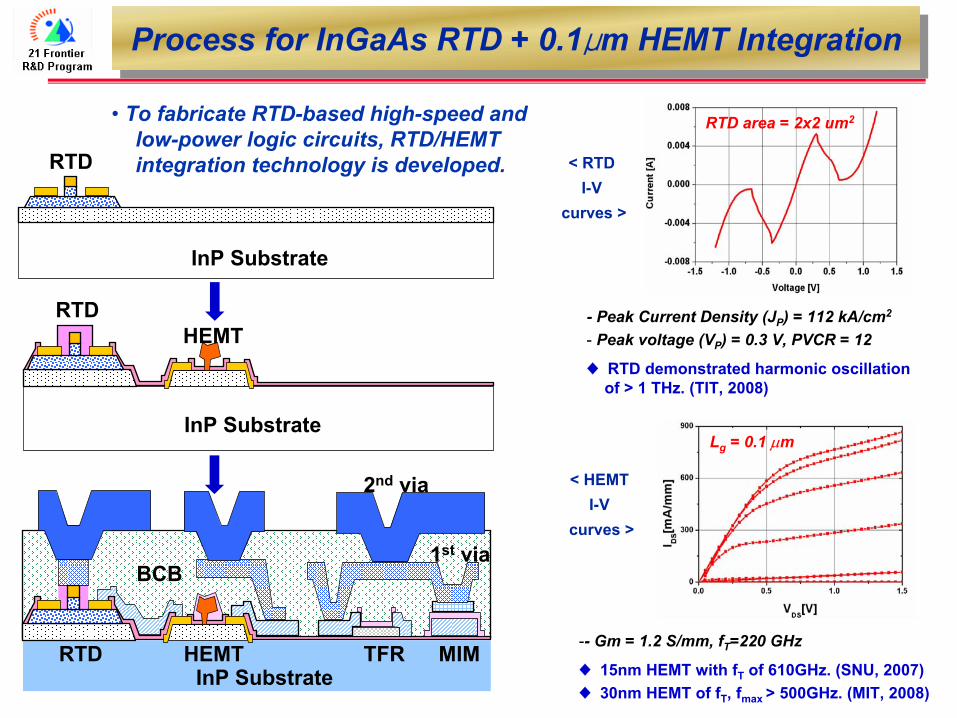
Process for InGaAs RTD + 0.1μm HEMT IntegrationProcess for InGaAs RTD + 0.1μm HEMT Integration
InP Substrate
RTD
InP Substrate
RTDHEMT
InP SubstrateRTD HEMT TFR MIM
BCB1st via
2nd via
• To fabricate RTD-based high-speed and low-power logic circuits, RTD/HEMTintegration technology is developed. < RTD
I-Vcurves >
RTD area = 2x2 um2
Lg = 0.1 µm
- Peak Current Density (JP) = 112 kA/cm2
- Peak voltage (VP) = 0.3 V, PVCR = 12
♦ RTD demonstrated harmonic oscillationof > 1 THz. (TIT, 2008)
< HEMT I-V
curves >
-- Gm = 1.2 S/mm, fT=220 GHz
♦ 15nm HEMT with fT of 610GHz. (SNU, 2007)♦ 30nm HEMT of fT, fmax > 500GHz. (MIT, 2008)
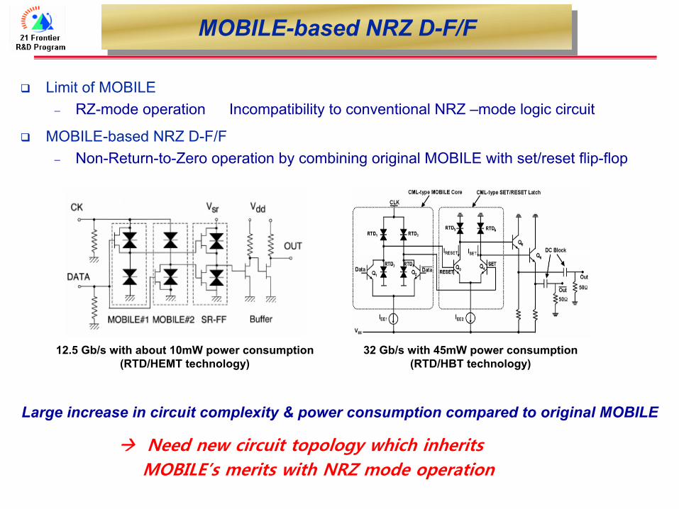
MOBILE-based NRZ D-F/FMOBILE-based NRZ D-F/F
Limit of MOBILE− RZ-mode operation Incompatibility to conventional NRZ –mode logic circuit
MOBILE-based NRZ D-F/F− Non-Return-to-Zero operation by combining original MOBILE with set/reset flip-flop
Need new circuit topology which inheritsMOBILE’s merits with NRZ mode operation
12.5 Gb/s with about 10mW power consumption(RTD/HEMT technology)
32 Gb/s with 45mW power consumption(RTD/HBT technology)
Large increase in circuit complexity & power consumption compared to original MOBILE
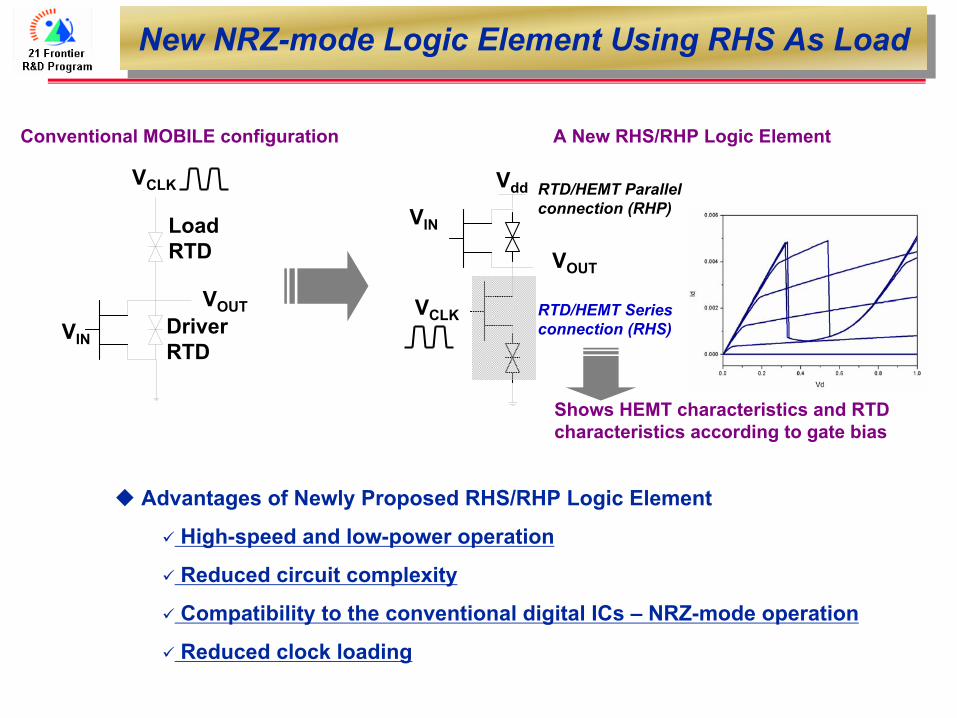
New NRZ-mode Logic Element Using RHS As LoadNew NRZ-mode Logic Element Using RHS As Load
Conventional MOBILE configuration A New RHS/RHP Logic Element
VCLK
VIN
Load RTD
DriverRTD
VCLKVOUT
VIN
Vdd
VOUT
RTD/HEMT Series connection (RHS)
RTD/HEMT Parallel connection (RHP)
Shows HEMT characteristics and RTD characteristics according to gate bias
Advantages of Newly Proposed RHS/RHP Logic Element
High-speed and low-power operation
Reduced circuit complexity
Compatibility to the conventional digital ICs – NRZ-mode operation
Reduced clock loading
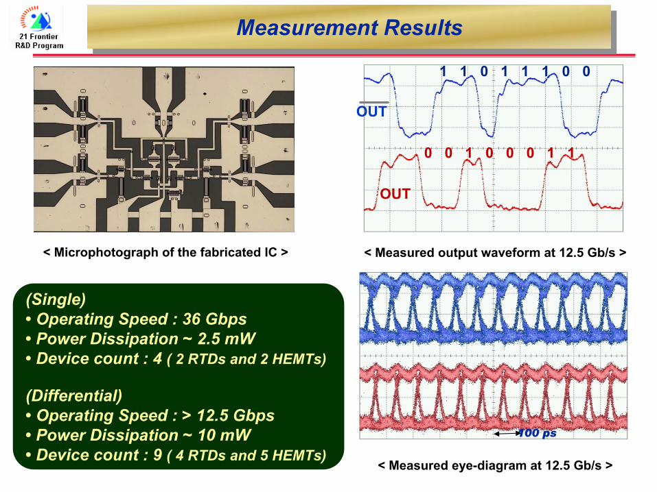
Measurement ResultsMeasurement Results
< Microphotograph of the fabricated IC > < Measured output waveform at 12.5 Gb/s >
< Measured eye-diagram at 12.5 Gb/s >
100 ps
1 1 0 1 1 1 0 0
0 0 1 0 0 0 1 1
OUT
OUT
(Single)• Operating Speed : 36 Gbps• Power Dissipation ~ 2.5 mW • Device count : 4 ( 2 RTDs and 2 HEMTs)
(Differential)• Operating Speed : > 12.5 Gbps• Power Dissipation ~ 10 mW • Device count : 9 ( 4 RTDs and 5 HEMTs)
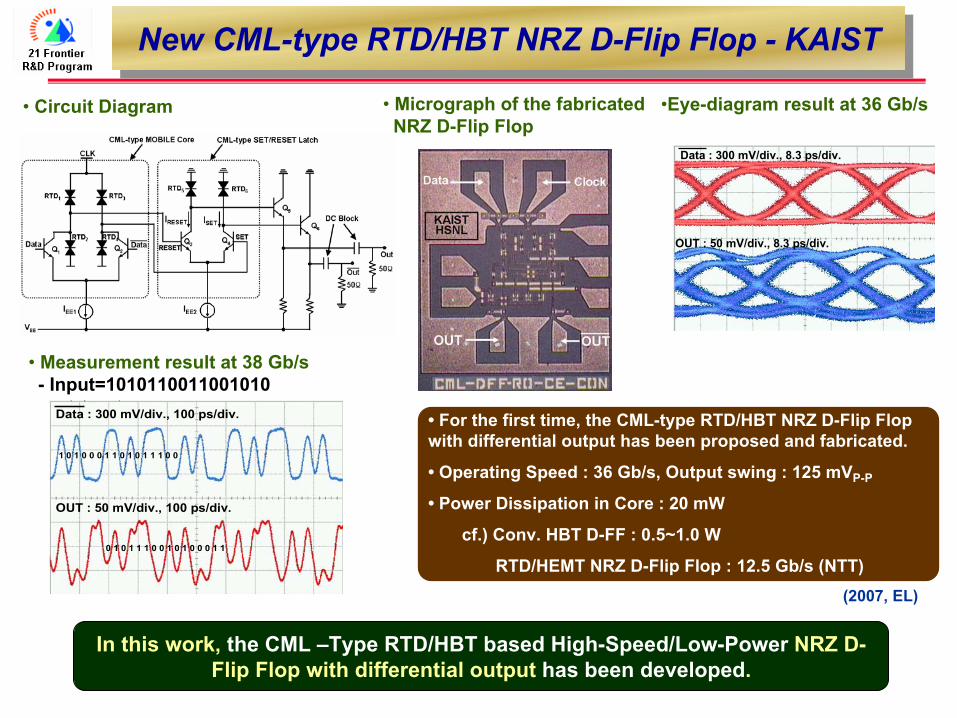
• For the first time, the CML-type RTD/HBT NRZ D-Flip Flop with differential output has been proposed and fabricated.
• Operating Speed : 36 Gb/s, Output swing : 125 mVP-P
• Power Dissipation in Core : 20 mW
cf.) Conv. HBT D-FF : 0.5~1.0 W
RTD/HEMT NRZ D-Flip Flop : 12.5 Gb/s (NTT)
• Micrograph of the fabricated NRZ D-Flip Flop
•Eye-diagram result at 36 Gb/s• Circuit Diagram
• Measurement result at 38 Gb/s- Input=1010110011001010
Data : 300 mV/div., 8.3 ps/div.
OUT : 50 mV/div., 8.3 ps/div.
1 0 1 0 0 0 1 1 0 1 0 1 1 1 0 0
0 1 0 1 1 1 0 0 1 0 1 0 0 0 1 1
Data : 300 mV/div., 100 ps/div.
OUT : 50 mV/div., 100 ps/div.
(2007, EL)
In this work, the CML –Type RTD/HBT based High-Speed/Low-Power NRZ D-Flip Flop with differential output has been developed.
New CML-type RTD/HBT NRZ D-Flip Flop - KAISTNew CML-type RTD/HBT NRZ D-Flip Flop - KAIST
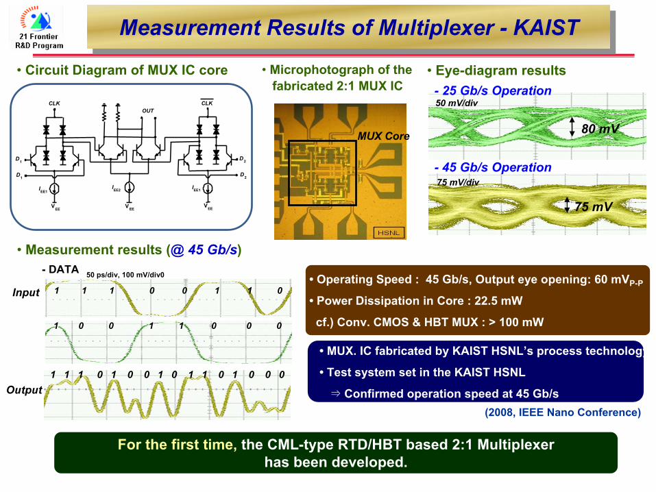
• Eye-diagram results• Circuit Diagram of MUX IC core
50 mV/div
- 45 Gb/s Operation
MUX Core
- DATA
1 1 1 0 1 0 0 1 0 1 1 0 1 0 0 0
1 0 0 1 1 0 0 0
Input
Output
50 ps/div, 100 mV/div0
1 1 1 0 0 1 1 0
75 mV/div
80 mV
75 mV
•동작속도 : 45 Gb/s, 출력크기: 75 mVP-P
•전력소모 : 22.5 mW
cf.) 기존 CMOS & HBT MUX의전력소모 : > 100 mW
- 25 Gb/s Operation• Microphotograph of the
fabricated 2:1 MUX IC
• Measurement results (@ 45 Gb/s)
(2008, IEEE Nano Conference)
• Operating Speed : 45 Gb/s, Output eye opening: 60 mVP-P
• Power Dissipation in Core : 22.5 mW
cf.) Conv. CMOS & HBT MUX : > 100 mW
• MUX. IC fabricated by KAIST HSNL’s process technology
• Test system set in the KAIST HSNL
⇒ Confirmed operation speed at 45 Gb/s
For the first time, the CML-type RTD/HBT based 2:1 Multiplexer has been developed.
D1
D1
D2
D2
CLK CLKOUT
IEE1IEE1IEE2
VEE VEE
VEE
Measurement Results of Multiplexer - KAISTMeasurement Results of Multiplexer - KAIST
RZ MOBILE using only RTDs as active devicesRZ MOBILE using only RTDs as active devices
[ Circuit configuration ]
OUTDATA
CLK
[ Microphotograph of MOBILE ]
OUT = 0 1 1 1 0 1 1 1
DATA = 0 1 1 1 0 1 1 1
700 mV
40 mV
50 ps
[ Measurement result at 40 Gbps ]
• To fully exploit high-speed/low-power characteristics of RTDs, MOBILE using only
RTDs is designed and demonstrated up to 40 Gbps with very low-power dissipation
about 0.86 mW
• Minimum power-delay product of about 22 fJ was obtained by considering AC current
effect of MOBILE and designing MOBILE using only RTDs without TRsCf.) 42 fJ using RTD/Schottky diode, 48 fJ using RTD/HEMT, and 96 fJ using RTD/UTC-PD
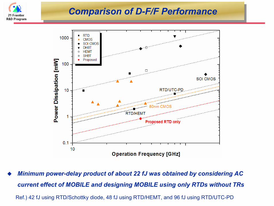
Comparison of D-F/F PerformanceComparison of D-F/F Performance
Minimum power-delay product of about 22 fJ was obtained by considering AC
current effect of MOBILE and designing MOBILE using only RTDs without TRs
Ref.) 42 fJ using RTD/Schottky diode, 48 fJ using RTD/HEMT, and 96 fJ using RTD/UTC-PD
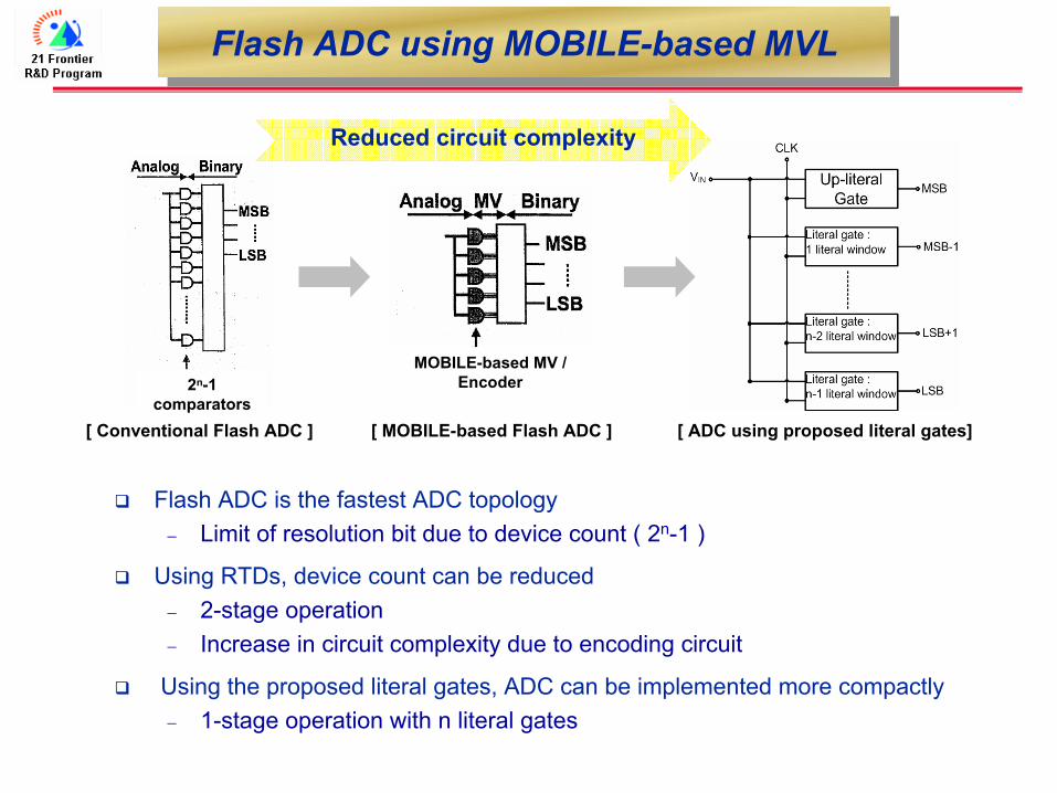
Flash ADC using MOBILE-based MVLFlash ADC using MOBILE-based MVL
Flash ADC is the fastest ADC topology− Limit of resolution bit due to device count ( 2n-1 )
Using RTDs, device count can be reduced− 2-stage operation− Increase in circuit complexity due to encoding circuit
Using the proposed literal gates, ADC can be implemented more compactly− 1-stage operation with n literal gates
[ Conventional Flash ADC ]
2n-1 comparators
[ MOBILE-based Flash ADC ]
MOBILE-based MV / Encoder
[ ADC using proposed literal gates]
Reduced circuit complexity
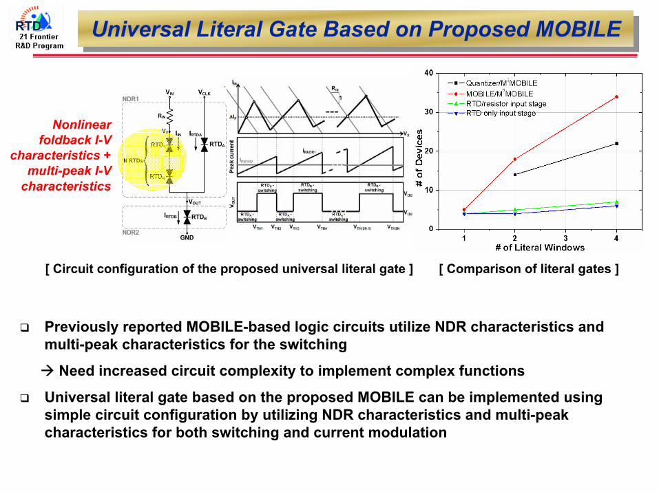
Universal Literal Gate Based on Proposed MOBILEUniversal Literal Gate Based on Proposed MOBILE
Nonlinear foldback I-V
characteristics + multi-peak I-V
characteristics
[ Circuit configuration of the proposed universal literal gate ] [ Comparison of literal gates ]
Previously reported MOBILE-based logic circuits utilize NDR characteristics and multi-peak characteristics for the switching
Need increased circuit complexity to implement complex functions
Universal literal gate based on the proposed MOBILE can be implemented using simple circuit configuration by utilizing NDR characteristics and multi-peak characteristics for both switching and current modulation
RTD
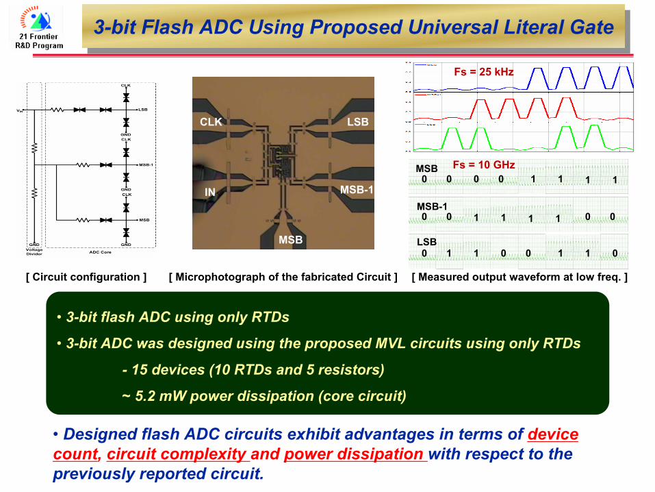
3-bit Flash ADC Using Proposed Universal Literal Gate3-bit Flash ADC Using Proposed Universal Literal Gate
[ Circuit configuration ] [ Microphotograph of the fabricated Circuit ] [ Measured output waveform at low freq. ]
IN
CLK
MSB
MSB-1
LSB
• 3-bit flash ADC using only RTDs
• 3-bit ADC was designed using the proposed MVL circuits using only RTDs
- 15 devices (10 RTDs and 5 resistors)
~ 5.2 mW power dissipation (core circuit)
MSB
LSB
MSB-1
0 1 10 1 100
1 11 100 00
1 1 1 100 00
Fs = 25 kHz
Fs = 10 GHz
• Designed flash ADC circuits exhibit advantages in terms of device count, circuit complexity and power dissipation with respect to the previously reported circuit.
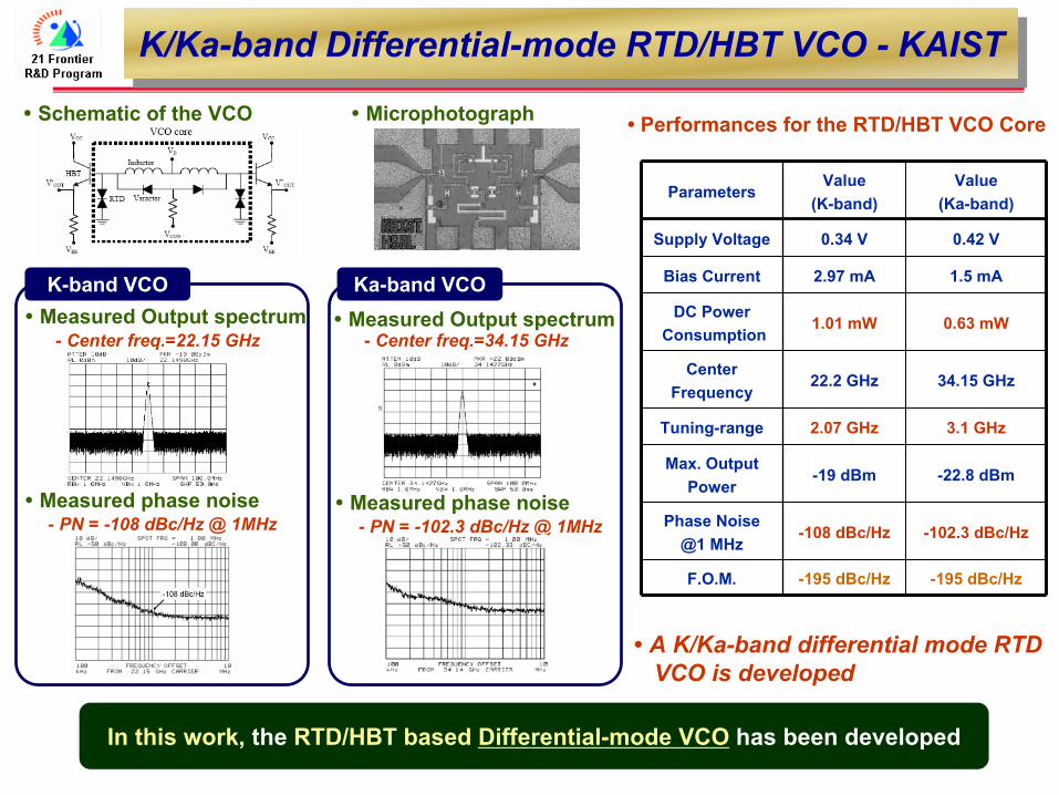
Schematic of the VCO Microphotograph
Measured Output spectrum
Measured phase noise
- Center freq.=22.15 GHz
- PN = -108 dBc/Hz @ 1MHz
K-band VCO Ka-band VCOMeasured Output spectrum
- Center freq.=34.15 GHz
Measured phase noise - PN = -102.3 dBc/Hz @ 1MHz
ParametersValue
(K-band)Value
(Ka-band)
Supply Voltage 0.34 V 0.42 V
Bias Current 2.97 mA 1.5 mA
DC PowerConsumption
1.01 mW 0.63 mW
Center Frequency
22.2 GHz 34.15 GHz
Tuning-range 2.07 GHz 3.1 GHz
Max. Output Power
-19 dBm -22.8 dBm
Phase Noise @1 MHz
-108 dBc/Hz -102.3 dBc/Hz
F.O.M. -195 dBc/Hz -195 dBc/Hz
• Performances for the RTD/HBT VCO Core
• A K/Ka-band differential mode RTDVCO is developed
In this work, the RTD/HBT based Differential-mode VCO has been developed
K/Ka-band Differential-mode RTD/HBT VCO - KAISTK/Ka-band Differential-mode RTD/HBT VCO - KAIST
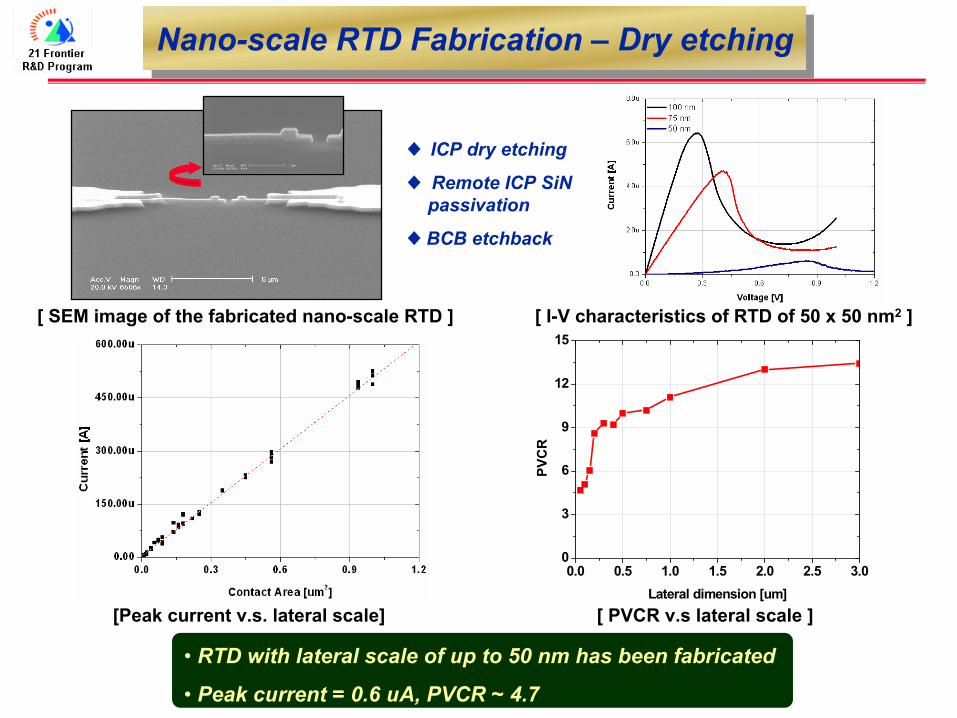
Nano-scale RTD Fabrication – Dry etchingNano-scale RTD Fabrication – Dry etching
[Peak current v.s. lateral scale] [ PVCR v.s lateral scale ]
[ I-V characteristics of RTD of 50 x 50 nm2 ][ SEM image of the fabricated nano-scale RTD ]
0.0 0.5 1.0 1.5 2.0 2.5 3.00
3
6
9
12
15
PVC
R
Lateral dimension [um]
• RTD with lateral scale of up to 50 nm has been fabricated
• Peak current = 0.6 uA, PVCR ~ 4.7
♦ ICP dry etching
♦ Remote ICP SiNpassivation
♦ BCB etchback
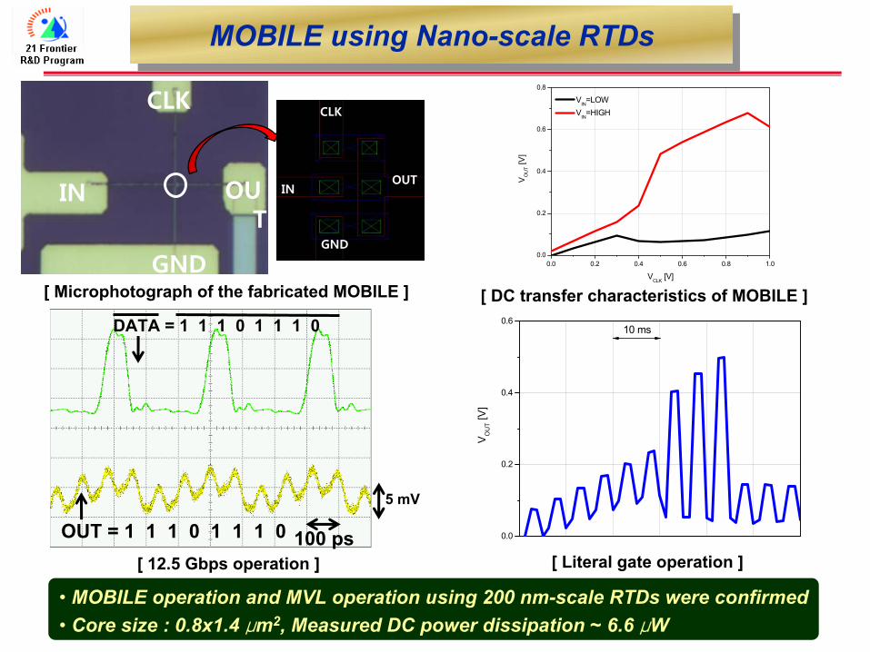
MOBILE using Nano-scale RTDsMOBILE using Nano-scale RTDs
[ 12.5 Gbps operation ] [ Literal gate operation ]
[ DC transfer characteristics of MOBILE ][ Microphotograph of the fabricated MOBILE ]
0.0 0.2 0.4 0.6 0.8 1.00.0
0.2
0.4
0.6
0.8
VO
UT [
V]
VCLK [V]
VIN=LOW VIN=HIGH
0.0
0.2
0.4
0.6
V OU
T [V
]
10 ms
CLK
IN
GND
OUT
DATA = 1 1 1 0 1 1 1 0
OUT = 1 1 1 0 1 1 1 0 100 ps
5 mV
CLK
IN
GND
OUT
• MOBILE operation and MVL operation using 200 nm-scale RTDs were confirmed• Core size : 0.8x1.4 μm2, Measured DC power dissipation ~ 6.6 μW
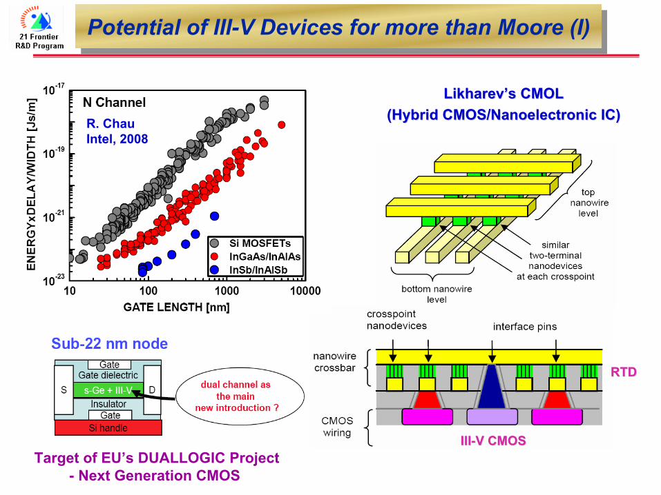
Potential of III-V Devices for more than Moore (I)Potential of III-V Devices for more than Moore (I)
LikharevLikharev’’ss CMOLCMOL(Hybrid CMOS/(Hybrid CMOS/NanoelectronicNanoelectronic IC)IC)
RTDRTD
IIIIII--V CMOSV CMOS
R. ChauIntel, 2008
Target of EU’s DUALLOGIC Project- Next Generation CMOS
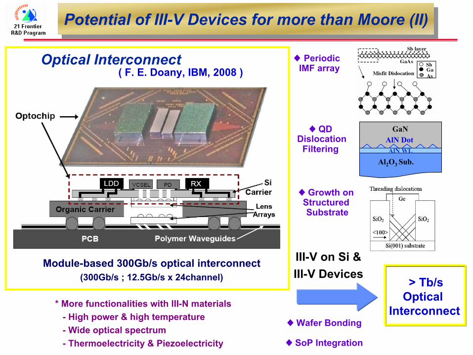
Potential of III-V Devices for more than Moore (II)Potential of III-V Devices for more than Moore (II)
( F. E. Doany, IBM, 2008 )
Module-based 300Gb/s optical interconnect(300Gb/s ; 12.5Gb/s x 24channel) > Tb/s
Optical Interconnect
III-V on Si &III-V Devices
Optical Interconnect ♦ PeriodicIMF array
AlN WLAlN Dot
Al2O3 Sub.
GaN♦ QDDislocation
Filtering
♦ Growth on StructuredSubstrate
♦Wafer Bonding
♦ SoP Integration
* More functionalities with III-N materials- High power & high temperature- Wide optical spectrum- Thermoelectricity & Piezoelectricity
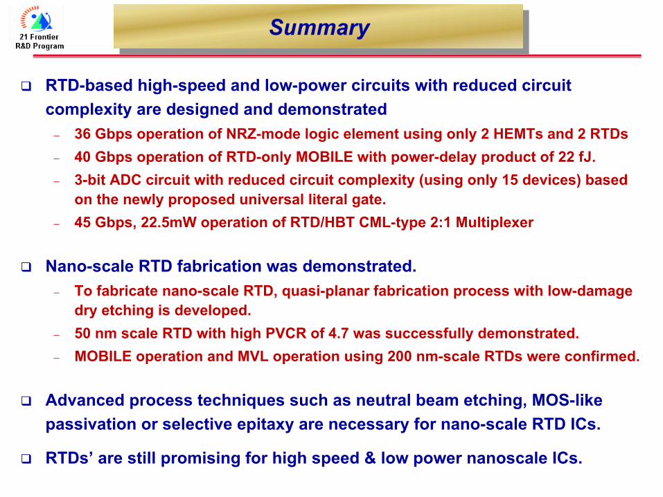
SummarySummary
RTD-based high-speed and low-power circuits with reduced circuit complexity are designed and demonstrated− 36 Gbps operation of NRZ-mode logic element using only 2 HEMTs and 2 RTDs− 40 Gbps operation of RTD-only MOBILE with power-delay product of 22 fJ.− 3-bit ADC circuit with reduced circuit complexity (using only 15 devices) based
on the newly proposed universal literal gate. − 45 Gbps, 22.5mW operation of RTD/HBT CML-type 2:1 Multiplexer
Nano-scale RTD fabrication was demonstrated.− To fabricate nano-scale RTD, quasi-planar fabrication process with low-damage
dry etching is developed.− 50 nm scale RTD with high PVCR of 4.7 was successfully demonstrated.− MOBILE operation and MVL operation using 200 nm-scale RTDs were confirmed.
Advanced process techniques such as neutral beam etching, MOS-like passivation or selective epitaxy are necessary for nano-scale RTD ICs.
RTDs’ are still promising for high speed & low power nanoscale ICs.

Thank You for Your Attention !
Any Questions ?